KR20060117171A - A method for forming a high-resolution pattern and a method for manufacturing a high- - Google Patents
A method for forming a high-resolution pattern and a method for manufacturing a high-Download PDFInfo
- Publication number
- KR20060117171A KR20060117171AKR1020060004609AKR20060004609AKR20060117171AKR 20060117171 AKR20060117171 AKR 20060117171AKR 1020060004609 AKR1020060004609 AKR 1020060004609AKR 20060004609 AKR20060004609 AKR 20060004609AKR 20060117171 AKR20060117171 AKR 20060117171A
- Authority
- KR
- South Korea
- Prior art keywords
- sacrificial layer
- pattern
- resolution
- substrate
- forming
- Prior art date
- Legal status (The legal status is an assumption and is not a legal conclusion. Google has not performed a legal analysis and makes no representation as to the accuracy of the status listed.)
- Granted
Links
Images


Classifications
- C—CHEMISTRY; METALLURGY
- C09—DYES; PAINTS; POLISHES; NATURAL RESINS; ADHESIVES; COMPOSITIONS NOT OTHERWISE PROVIDED FOR; APPLICATIONS OF MATERIALS NOT OTHERWISE PROVIDED FOR
- C09D—COATING COMPOSITIONS, e.g. PAINTS, VARNISHES OR LACQUERS; FILLING PASTES; CHEMICAL PAINT OR INK REMOVERS; INKS; CORRECTING FLUIDS; WOODSTAINS; PASTES OR SOLIDS FOR COLOURING OR PRINTING; USE OF MATERIALS THEREFOR
- C09D11/00—Inks
- C09D11/30—Inkjet printing inks
- H—ELECTRICITY
- H01—ELECTRIC ELEMENTS
- H01L—SEMICONDUCTOR DEVICES NOT COVERED BY CLASS H10
- H01L21/00—Processes or apparatus adapted for the manufacture or treatment of semiconductor or solid state devices or of parts thereof
- H01L21/02—Manufacture or treatment of semiconductor devices or of parts thereof
- H01L21/04—Manufacture or treatment of semiconductor devices or of parts thereof the devices having potential barriers, e.g. a PN junction, depletion layer or carrier concentration layer
- H01L21/18—Manufacture or treatment of semiconductor devices or of parts thereof the devices having potential barriers, e.g. a PN junction, depletion layer or carrier concentration layer the devices having semiconductor bodies comprising elements of Group IV of the Periodic Table or AIIIBV compounds with or without impurities, e.g. doping materials
- H01L21/30—Treatment of semiconductor bodies using processes or apparatus not provided for in groups H01L21/20 - H01L21/26
- H01L21/31—Treatment of semiconductor bodies using processes or apparatus not provided for in groups H01L21/20 - H01L21/26 to form insulating layers thereon, e.g. for masking or by using photolithographic techniques; After treatment of these layers; Selection of materials for these layers
- H01L21/32—Treatment of semiconductor bodies using processes or apparatus not provided for in groups H01L21/20 - H01L21/26 to form insulating layers thereon, e.g. for masking or by using photolithographic techniques; After treatment of these layers; Selection of materials for these layers using masks
- H—ELECTRICITY
- H01—ELECTRIC ELEMENTS
- H01L—SEMICONDUCTOR DEVICES NOT COVERED BY CLASS H10
- H01L21/00—Processes or apparatus adapted for the manufacture or treatment of semiconductor or solid state devices or of parts thereof
- H01L21/02—Manufacture or treatment of semiconductor devices or of parts thereof
- H01L21/02104—Forming layers
- H01L21/02107—Forming insulating materials on a substrate
- H01L21/02109—Forming insulating materials on a substrate characterised by the type of layer, e.g. type of material, porous/non-porous, pre-cursors, mixtures or laminates
- H01L21/02112—Forming insulating materials on a substrate characterised by the type of layer, e.g. type of material, porous/non-porous, pre-cursors, mixtures or laminates characterised by the material of the layer
- H01L21/02118—Forming insulating materials on a substrate characterised by the type of layer, e.g. type of material, porous/non-porous, pre-cursors, mixtures or laminates characterised by the material of the layer carbon based polymeric organic or inorganic material, e.g. polyimides, poly cyclobutene or PVC
- H—ELECTRICITY
- H01—ELECTRIC ELEMENTS
- H01L—SEMICONDUCTOR DEVICES NOT COVERED BY CLASS H10
- H01L21/00—Processes or apparatus adapted for the manufacture or treatment of semiconductor or solid state devices or of parts thereof
- H01L21/02—Manufacture or treatment of semiconductor devices or of parts thereof
- H01L21/02104—Forming layers
- H01L21/02107—Forming insulating materials on a substrate
- H01L21/02225—Forming insulating materials on a substrate characterised by the process for the formation of the insulating layer
- H01L21/0226—Forming insulating materials on a substrate characterised by the process for the formation of the insulating layer formation by a deposition process
- H01L21/02282—Forming insulating materials on a substrate characterised by the process for the formation of the insulating layer formation by a deposition process liquid deposition, e.g. spin-coating, sol-gel techniques, spray coating
- H01L21/02288—Forming insulating materials on a substrate characterised by the process for the formation of the insulating layer formation by a deposition process liquid deposition, e.g. spin-coating, sol-gel techniques, spray coating printing, e.g. ink-jet printing
Landscapes
- Engineering & Computer Science (AREA)
- Chemical & Material Sciences (AREA)
- Condensed Matter Physics & Semiconductors (AREA)
- General Physics & Mathematics (AREA)
- Manufacturing & Machinery (AREA)
- Computer Hardware Design (AREA)
- Microelectronics & Electronic Packaging (AREA)
- Power Engineering (AREA)
- Physics & Mathematics (AREA)
- Materials Engineering (AREA)
- Life Sciences & Earth Sciences (AREA)
- Wood Science & Technology (AREA)
- Organic Chemistry (AREA)
- Exposure And Positioning Against Photoresist Photosensitive Materials (AREA)
- Internal Circuitry In Semiconductor Integrated Circuit Devices (AREA)
- Application Of Or Painting With Fluid Materials (AREA)
- Manufacturing Of Printed Wiring (AREA)
- Electroluminescent Light Sources (AREA)
- Exposure Of Semiconductors, Excluding Electron Or Ion Beam Exposure (AREA)
- Electrodes Of Semiconductors (AREA)
- Thin Film Transistor (AREA)
Abstract
Translated fromKoreanDescription
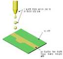
Translated fromKorean도 1은 종래의 잉크젯 패턴법에 의해 패턴을 형성하는 방법에 대한 개략적인 순서도이다.1 is a schematic flowchart of a method of forming a pattern by a conventional ink-jet pattern method.
도 2는 종래의 레이저 패턴법에 의해 패턴을 형성하는 방법에 대한 개략적인 순서도이다.2 is a schematic flowchart of a method of forming a pattern by a conventional laser patterning method.
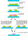
도 3은 본 발명에 따른 패터닝 방법에 대한 개략적인 순서도이다.3 is a schematic flow chart of a patterning method according to the present invention.
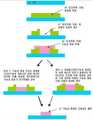
도 4는 본 발명에 따라 부분적으로 고해상도 패턴을 형성하는 방법에 대한 개략적인 순서도이다.Figure 4 is a schematic flow diagram of a method for forming a partially high resolution pattern in accordance with the present invention.
도 5와 도 6은 각각 희생층 형성용 물질로 저분자계열과 고분자계열을 사용했을 때 레이저로 패턴 형성용 재료가 적층될 부분을 제거했을 때의 양상을 나타낸 것이다.FIGS. 5 and 6 illustrate patterns when the low-molecular-based and polymer-based materials are used as the sacrificial layer-forming material, respectively, and portions where the pattern-forming material is to be laminated with a laser are removed.
도 7과 도 8은 각각 저분자계열과 고분자계열의 희생층 형성용 물질을 사용했을 경우의 실시예의 순서도이다.FIGS. 7 and 8 are flowcharts of embodiments in which a sacrificial layer forming material of low molecular weight and high molecular weight is used, respectively.
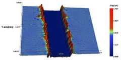
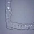
도 9는 본 발명의 실시예 1에서 희생층이 부분적으로 제거된 패턴에 대한 광학현미경사진이다.9 is an optical microscope photograph of a pattern in which a sacrificial layer is partially removed in Example 1 of the present invention.
도 10은 본 발명의 실시예 1에 의해 제조된 폴리스티렌 패턴에 대한 광학현미경사진이다.10 is an optical microscope photograph of the polystyrene pattern produced by Example 1 of the present invention.
<도면의 주요부분에 대한 부호의 설명>Description of the Related Art
1…잉크젯 프린트 헤드와 그에 의해 생성된 잉크방울One… The inkjet printhead and the ink drops produced thereby
10...기판10 ... substrate
20...잉크젯에 의해 형성된 기능성 재료의 저해상도 패턴20 ... low resolution pattern of functional material formed by inkjet
21...본 발명에 의해 형성된 기능성 재료의 고해상도 패턴21 ... High-resolution pattern of the functional material formed by the present invention
30...희생층31...부분적 제거영역 40...기능성 재료30 ... sacrificial layer 31 ... partially removed region 40 ... functional material
본 발명은 고해상도 패턴형성방법 및 상기 방법에 따라 프리패턴이 형성된 기판에 관한 것이다.The present invention relates to a high-resolution pattern formation method and a substrate on which a pre-pattern is formed according to the method.
전자소자에 사용되는 고해상도의 패턴을 형성하는 방법으로는 종래에 포토리소그라피가 가장 많이 사용되어 왔으나 재료낭비가 많고, 다단계 공정이며, 포토마스크, 포토레지스트, 현상액, 식각용액을 사용하는 등 공정이 복잡하기 때문에 공정효율이 떨어지며, 대면적 마스크를 사용해야 하기 때문에 새로운 설계를 최단시간내에 생산라인에 적용하는데에 어려움이 있다는 등의 단점이 있었다. 따라서, 포토리소그라피의 이러한 단점들을 극복하기 위해, 적은 공정수와 재료낭비를 최소화한 채로 마스크없이 직접적으로 기판상에 패턴을 행할 수 있는 방법으로서 잉크젯 패턴법이 개발되었다.As a method of forming a high-resolution pattern used in an electronic device, photolithography has been used most often, but a lot of material waste is involved, and a multistage process is used. A photomask, a photoresist, a developing solution, It is difficult to apply the new design to the production line in the shortest time because the process efficiency is low and the large area mask must be used. Therefore, in order to overcome these shortcomings of photolithography, an ink-jet pattern method has been developed as a method capable of directly performing a pattern on a substrate without a mask while minimizing the number of process wastes and material waste.
EP-A-O 880303 및 대한민국 공개특허공보 제2004-28972에는 마스크를 사용하지 않고 잉크젯 방법에 의해 직접 패턴을 형성하는 방법이 알려져 있으며, 도 1에 상기 잉크젯 방법을 통해 패턴을 형성하는 방법에 대한 개략적인 순서도를 도시하였다. 그러나, 마이크로 일렉트로닉스 등의 미세소자에 적용하기에는 해상도가 너무 낮으며, 잉크방울이 작아질수록 패턴의 위치오차가 기판에 적층될 잉크방울에 비해 상대적으로 증대하여 치명적인 단락(open circuit) 혹은 합선(short circuit) 을 발생시킬 수 있다는 문제점이 있었다.EP-AO 880303 and Korean Patent Laid-Open Publication No. 2004-28972 disclose a method of directly forming a pattern by an ink-jet method without using a mask. FIG. 1 shows a schematic view of a method of forming a pattern through the ink- FIG. However, the resolution is too low for application to micro devices such as microelectronics, and as the ink droplet is smaller, the positional error of the pattern increases relative to the ink droplets to be stacked on the substrate, resulting in a fatal open circuit or short circuit ) Can be generated.
또한, 대한민국 공개특허공보 제2000-5446호에는 레이저를 이용하여 직접 패터닝을 형성하는 방법이 개시되어 있으며, 도 2에는 상기 레이저 패턴법에 의해 패턴을 형성하는 방법에 대한 개략적인 순서도를 도시하였다. 도 2를 참조하면, 전사필름 상에 LTHC(light-to-heat conversion) 물질을 스핀코팅법 등으로 코팅하여 LTHC 층(전사층)을 형성한 후, 기능성 재료 및 점착조절용 첨가제를 혼합한 조성물을 상기 LTHC 상부에 스핀코팅법 등으로 코팅함으로써 도너 필름을 제작한 다음 이를 기판과 점착시키고, 레이저를 조사함으로써 패턴을 전사시킨 후, 최종적으로 전사후의 도너 필름을 제거하는 것에 의해 고해상도의 패턴을 제작할 수 있다. 그러나, 도너 필름을 별도로 제작해야 하기 때문에 제조단가가 상승되며, 도너필름 전체에 패턴화시킬 기능성 재료를 코팅해야 하므로 기능성 재료의 낭비가 심하고, 기능성 재료에 첨가되는 첨가제에 의한 재료특성의 저감, 또는 도너필름과 기판의 점착시 기판과 도너필름 간의 오염문제, 레이저에 의해 발생된 높은 온도에 의한 재 료열화 등이 발생할 염려가 있었다.Korean Patent Laid-Open Publication No. 2000-5446 discloses a method of forming a pattern directly using a laser. FIG. 2 shows a schematic flowchart of a method of forming a pattern by the laser pattern method. 2, a composition in which a LTHC layer (transfer layer) is formed by coating a light-to-heat conversion material on a transfer film by spin coating or the like and then mixing a functional material and an additive for controlling adhesion A donor film is formed on the LTHC by spin coating or the like, and then the donor film is adhered to the substrate. Then, the pattern is transferred by irradiating a laser beam, and finally, the donor film after the transfer is removed. have. However, since the donor film must be separately prepared, the manufacturing cost is increased, and the functional material to be patterned is coated on the entire donor film, so that the waste of the functional material is wasted and the material property is reduced by the additive added to the functional material. There is a possibility that contamination between the substrate and the donor film during adhesion of the donor film and the substrate and deterioration of the material due to the high temperature generated by the laser may occur.
한편, 레이저를 이용한 다른 패턴형성방법으로는 레이저 어블레이션을 들 수 있는데, 이는 어블레이션을 할 패턴의 재질에 따라 사용되는 레이저 파장에 대한 효율이 다르며, 레이저 사용량을 미세하게 조절할 필요가 있고, 다층구조의 패터닝시 패턴 혹은 기판, 이미 적층된 하부패턴의 손상염려가 있다는 문제점이 있었다.On the other hand, another pattern forming method using a laser is laser ablation. This is because the efficiency with respect to the laser wavelength used differs depending on the material of the pattern to be ablated, the laser use amount needs to be finely adjusted, There is a risk that the pattern or the substrate or the underlying pattern that has already been laminated may be damaged when the structure is patterned.
따라서, 본 발명은 고해상도의 패터닝이 가능하며, 공정효율이 높고 고비용의 기능성 재료의 낭비가 적은 패턴형성 방법 및 상기 패턴형성 방법에 따라 프리패턴이 형성된 기판을 제공하고자 한다.Accordingly, it is an object of the present invention to provide a pattern forming method capable of high-resolution patterning, high process efficiency and low cost of functional materials, and a substrate on which a pre-pattern is formed according to the pattern forming method.
본 발명은 제1물질로 된 희생층이 부분 또는 전면 형성된 기판을 제공하는 제1단계; 제1수단으로 희생층에 제1물질이 존재하지 않으면서 선폭이 최고 제1해상도를 갖는 패턴 홈을 형성하는 제2단계; 제2수단을 사용하여 제2물질을 상기 패턴 홈에 충진하는 제3단계; 및 광 또는 열 조사에 의해 잔여 희생층에 존재하는 제1물질을 제거하는 제4단계를 포함하며, 제1물질의 최소 경계 조사량(threshold fluence)이 제2물질의 최소 경계 조사량 보다 작고, 제4단계에서 제1물질의 최소 경계 조사량 이상 제2물질의 최소 경계 조사량 미만의 조사량으로 제1물질을 제거하는 것이 특징인 기판상에 제2물질로 패턴을 형성하는 방법을 제공한다.The present invention provides a method of manufacturing a semiconductor device, comprising: a first step of providing a sacrificial layer of a first material with a partially or entirely formed substrate; A first step of forming a pattern groove having a line width of the first resolution without sacrificing the first material in the sacrificial layer; A third step of filling a second material into the pattern groove using a second means; And a fourth step of removing the first material present in the remaining sacrificial layer by light or heat irradiation, wherein a threshold fluence of the first material is less than a minimum bound irradiance of the second material, Wherein the first material is removed at a dose less than the minimum bound irradiance of the second material by at least the minimum bound irradiance of the first material.
또한, 본 발명은 제1물질로 된 희생층이 부분 또는 전면 형성된 기판으로서, 상기 기판상의 희생층은 제1물질이 존재하지 않으면서 선폭이 최고 제1해상도를 갖 는 패턴 홈이 형성되어 있고, 제2물질이 최고 제1해상도를 갖는 패턴 홈에 충진되어 있으며, 제1물질의 최소 경계 조사량(threshold fluence)이 제2물질의 최소 경계 조사량 보다 작은 것이 특징인 프리패턴이 형성된 기판을 제공한다.The sacrificial layer on the substrate is formed with a pattern groove having a line width of the first highest resolution without the presence of the first material, Wherein the second material is filled in the pattern groove having the highest first resolution and the threshold fluence of the first material is less than the minimum bound irradiation amount of the second material.
이하, 첨부된 도면을 참조하여 본 발명을 더욱 상세히 설명한다.Hereinafter, the present invention will be described in more detail with reference to the accompanying drawings.
본 발명에서 어떤 물질에 대한 최소 경계 조사량이라 함은 일정 시간동안 집속 에너지 빔과 같은 광 또는 열을 조사하여 그 물질을 분해 또는 기화시킴으로써 제거할 수 있는 최소한의 에너지를 일컫는다.In the present invention, the minimum bound irradiation amount refers to the minimum energy that can be removed by irradiating light or heat such as a focused energy beam for a predetermined time to decompose or vaporize the material.
도 3에는 본 발명의 일 실시형태에 따른 패터닝 방법의 개략적인 순서도가 도시되어 있으며, 도 3을 참조하여 먼저 본 발명의 패턴 형성 방법을 설명한다.FIG. 3 is a schematic flow diagram of a patterning method according to an embodiment of the present invention. First, referring to FIG. 3, a pattern forming method of the present invention will be described.
(1)(One)제1물질로 된 희생층이 부분 또는 전면 형성된 기판을 제공하는 제1단계A first step of providing a sacrificial layer of a first material with a partially or fully formed substrate
기판 상에 희생층을 형성하는 방법은 당업계에서 일반적으로 사용되는 막형성법이 사용될 수 있으며, 특별히 제한되지 않는다.As a method of forming the sacrificial layer on the substrate, a film forming method commonly used in the art can be used and is not particularly limited.
희생층 형성용 제1물질은 슬릿코팅/스핀코팅 등과 같이 무패턴지향성 코팅방법을 통해 기판상에 전면도포, 또는 스크린 프린팅, 롤 프린팅 또는 잉크젯 프린팅 등을 통해 기판상에 패턴 지향적으로 선택적으로 부분도포될 수 있다.The first material for forming the sacrificial layer may be selectively applied to the substrate in a pattern-wise direction on the substrate through a full-surface coating on the substrate, or a screen printing, a roll printing, or an ink-jet printing, etc. by a patternless directional coating method such as a slit coating / .
희생층 형성용 제1물질이 액상 또는 반고체상인 경우에는, 잉크젯, 인쇄법, 스크린 프린팅법, 정전기 프린팅법, 오프셋 프린팅법, 그라비어 프린팅법, 플렉소 프린팅법, 소프트 몰드를 사용한 프린팅법 또는 스핀코팅법이나 슬릿코팅법을 사용할 수 있다. 한편, 희생층 형성용 제1물질이 고체상인 경우에는 집속 이온빔이나 플라즈마를 이용하여 스퍼터링할 수 있고, 희생층 형성용 제1물질이 고체상 또는 반고체상인 경우에는 이를 필름형태로 제조한 다음에 레이저를 사용하여 전사하여 직접 적층할 수도 있다.When the first material for forming the sacrificial layer is a liquid or semi-solid, it may be formed by ink jet, printing method, screen printing method, electrostatic printing method, offset printing method, gravure printing method, flexo printing method, Method or a slit coating method may be used. On the other hand, when the first material for forming the sacrificial layer is in a solid state, it can be sputtered using a focused ion beam or plasma. If the first material for sacrificial layer formation is a solid or semi-solid phase, Or may be directly laminated by transfer.
특히, 희생층 형성용 제1물질이 고비용일 경우, 직접 패턴법인 잉크젯법을 사용하여 형성하고자 하는 패턴 홈과 다른 해상도로, 바람직하게는 패턴 홈의 선폭 보다 낮은 해상도로 희생층을 기판상에 패턴 형성시킬 수 있다.Particularly, when the first material for forming the sacrificial layer is high in cost, the sacrificial layer is patterned on the substrate at a resolution different from that of the pattern groove to be formed by using the ink-jet method of the direct pattern method, preferably, .
상기 희생층을 적층시키고 나서 기판은 건조시키는 것이 바람직하다. 액체상의 희생층에서는 패턴 홈 형성 및 기능성 재료의 패턴 홈 충진을 할 수 없기 때문이다.Preferably, the sacrificial layer is laminated and then the substrate is dried. This is because pattern grooves can not be formed in the liquid phase sacrificial layer and pattern groove filling of the functional material can not be performed.
한편, 희생층은 이미 패턴된 영역들을 포함하는 기판 상에 형성될 수도 있다.On the other hand, the sacrificial layer may be formed on a substrate including already patterned regions.
(2) 제1수단으로 희생층에 제1물질이 존재하지 않으면서 선폭이 최고 제1해상도를 갖는 패턴 홈을 형성하는 제2단계(2) a second step of forming a pattern groove having a line width of the first resolution with no first material in the sacrificial layer by the first means
제2단계에서는 희생층을 원하는 형태로 선가공하여 제1물질이 존재하지 않는 고해상도의 패턴 홈을 형성하는 것이 바람직하다.In the second step, it is preferable to form the sacrificial layer into a desired shape to form a high-resolution pattern groove in which the first material is not present.
고해상도의 패턴 홈을 형성시킬 수 있는 제1수단으로는 E-beam, 집속 이온빔, 레이저, 광학계와 병행하여 사용하는 대출력 램프와 같이 작은 면적에 대용량의 에너지를 집속할 수 있는 집속 에너지빔이 바람직하며, 희생층 형성용 제1물질을 제거하는데 적합한 수단을 선택하여 사용할 수 있다.As a first means for forming a pattern groove of high resolution, a focused energy beam capable of focusing a large amount of energy in a small area such as an E-beam, a focused ion beam, a laser, and a large output lamp used in parallel with an optical system is preferable And a suitable means for removing the sacrificial layer forming first material may be selected and used.
여기서 대출력 램프는 원하는 소정 파장대의 빛을 방출하는 고출력의 램프를 의미하며, 예컨대 자외선 램프 또는 적외선 램프 등을 들 수 있으며, 렌즈와 같은 집속목적을 가지는 소자를 이용하여 집속하였을 때에 희생층을 충분히 제거할 수 있는 정도의 에너지 출력을 가지면 족하다.Here, the large-output lamp means a high-output lamp that emits light of a desired predetermined wavelength range. Examples of the high-output lamp include an ultraviolet lamp or an infrared lamp. When the light is focused using an element having a focusing purpose such as a lens, Having enough energy output to be removed is sufficient.
상기 고해상도의 패턴 홈의 형태로 희생층이 선택적으로 제거된 부분은 최종적으로 기능성 재료와 같은 패턴 형성용 제2물질이 패턴 지향적으로 충진되어 상기 제2물질이 기판상에 고해상도의 패턴으로 남아있게 될 부분에 해당한다.The portion where the sacrificial layer is selectively removed in the form of the pattern groove of high resolution is finally pattern-orientedly filled with the second pattern-forming material such as the functional material so that the second material remains in a high-resolution pattern on the substrate .
희생층에 패턴 홈을 형성시키는 제1수단으로 마스크 없이 직접 집속 에너지빔을 조사하는 방법(maskless direct energy beam writing)을 사용할 수 있으나, 제1수단으로 레이저 빔을 사용하는 경우 빔의 모양을 패터닝에 유리하게 조절하기 위하여 광학회절소자나 마스크를 부분적으로 사용할 수도 있다. 예컨대 마스크를 사용하고 레이저 스캐닝을 하는 방법(mask-based laser scanning) 혹은 회절광학소자 (diffractive optical element) 등을 사용하여 복잡한 형상의 패턴 홈을 희생층에 형성할 수 있다(도 4 중 (c) 참조).The first means for forming the pattern groove in the sacrificial layer may be a maskless direct energy beam writing method without using a mask. However, if the laser beam is used as the first means, Optical converters or masks may be used in part to advantageously control. A complicated pattern groove may be formed in the sacrificial layer by using a mask-based laser scanning method or a diffractive optical element using a mask (see (c) in FIG. 4) Reference).
이때 마스크의 사용은 기존의 리소그라피에서 대면적 패터닝을 위해 사용되는 마스크가 아닌 레이저 빔의 경로상에 위치하여 기판에 조사되는 빔의 형상을 제어하기 위해 국부적으로 사용되는 마스크를 의미한다. 빔의 형상 제어를 위해서 마스크보다는 회절광학소자가 선호되나 이에 특별히 국한되지는 않는다.The use of a mask herein refers to a mask used locally to control the shape of the beam irradiated onto the substrate, which is located on the path of the laser beam, rather than the mask used for large-area patterning in conventional lithography. For controlling the shape of the beam, a diffractive optical element is preferred rather than a mask, but not particularly limited thereto.
상기 광학회절소자나 마스크의 해상도는 제1수단을 사용하여 실현할 수 있는 최고 제1해상도 보다 높은 것이 바람직하다.It is preferable that the resolution of the optical isolator and the mask is higher than the highest first resolution that can be realized by using the first means.
본 발명에서, 패턴 홈의 해상도는 일반적으로 레이저와 같은 집속 에너지 빔으㎛㎛로 직접 패턴할 수 있는 최소 선폭까지 구현 가능하고, 장비에 따라서는 최 소 선폭이 서브마이크로미터까지 가능하다. 반대로 최대 선폭은 수백~수천 ㎛에 이른다.In the present invention, the resolution of the pattern grooves can be realized up to a minimum line width that can be directly patterned as a micrometer of a focused energy beam such as a laser, and a line width of up to a submicrometer is possible depending on equipment. On the contrary, the maximum line width is several hundreds to several thousands of 탆.
희생층 형성용 제1물질을 레이저에 의해 유도된 열로 분해/증발시켜 제거하는 경우에는 주로 가시광선 혹은 적외선 파장이 사용되며, 화학결합을 끊어서 제거하는 경우에는 주로 자외선 파장의 레이저를 사용하는 것이 바람직하다.When the first material for forming the sacrificial layer is decomposed / evaporated by laser induced heat to remove it, a visible light or an infrared light is mainly used. In the case of removing chemical bonds, it is preferable to use a laser of ultraviolet wavelength Do.
희생층 형성용 제1물질이, 사용되는 레이저의 파장에서 최대 흡광 스펙트럼을 보일 경우에는 흡광을 돕기위한 첨가제 없이 사용될 수도 있으나, 사용되는 파장대에서 최대 흡광 스펙트럼을 보이는 첨가제를 사용함으로써 제거를 용이하게 할 수도 있다. 첨가제로서 흡광제의 선택은 또한 희생층 형성용 제1물질을 용해하는 용액에 높은 용해도를 가지는 것이 바람직하다.When the first material for forming the sacrificial layer shows the maximum absorption spectrum at the wavelength of the laser used, it can be used without additives for assisting the absorption of light, but it is easy to remove by using the additive showing the maximum absorption spectrum at the used wavelength band It is possible. It is preferable that the selection of the light absorber as an additive also has a high solubility in a solution for dissolving the first substance for forming the sacrificial layer.
(3) 제2수단을 사용하여 제2물질을 상기 패턴 홈에 충진하는 제3단계(3) filling the pattern groove with the second material by using the second means;
기판상에 최종적으로 패턴을 형성하고자 하는 제2물질 예컨대 기능성 재료를 상기 패턴홈에 충진시킨다.A second material, such as a functional material, which is ultimately desired to form a pattern on the substrate, Fill the groove.
상기 제3단계는 직접 패턴이 가능한 제2수단을 사용하는 것이 바람직하다. 직접 패턴법이란, 최종적으로 패턴을 형성하게 될 물질을 원하는 곳에 직접적으로 적층하는 것을 의미한다.It is preferable that the third step uses a second means capable of direct patterning. By the direct pattern method, it is meant to directly laminate a material to be finally formed with a pattern to a desired place.
직접 패턴법은 포토리소그라피와 같은 subtractive process가 아닌 additive process이며 특히 잉크젯이나 레이저 직접 패턴법의 경우에는 CAD(computer aided design) to drawing이 가능하다.The direct pattern method is an additive process, not a subtractive process such as photolithography. In the case of inkjet or laser direct pattern method, CAD (computer aided design) drawing is possible.
직접 패턴이 가능한 제2수단을 사용하면, 패턴형성용 제2물질을 기판 전체에 대하여 적층하는 것이 아니라, 필요한 부분에만 부분적으로 적층할 수 있으므로 종래의 LTHC 도너 필름을 사용하는 패터닝방법보다 기능성 재료와 같은 패턴형성용 제2물질의 낭비가 현저히 줄어들게 된다.The use of the second means capable of direct patterning allows the second material for pattern formation not to be laminated over the entire substrate but to be partially laminated only on a necessary portion of the substrate so that the patterning method using the conventional LTHC donor film The waste of the second material for forming the same pattern is remarkably reduced.
본 발명은 패턴 형성용 제2물질로 기판 상에 패턴 형성시 저해상도의 제2수단을 사용하더라도, 고해상도의 제1수단을 사용하여 고해상도의 패턴 홈을 형성하고 이를 이용함으로써, 패턴 형성용 제2물질로 된 고해상도의 패턴을 형성할 수 있는 것을 특징으로 한다.The present invention is also applicable to a method for forming a pattern for forming a pattern on a substrate by forming and patterning a high resolution pattern groove using a first means of high resolution and using the second means for pattern formation, A high-resolution pattern having a high resolution can be formed.
상기 제3단계는 상기 제2단계에서 형성된 패턴 홈에 제2해상도로 제2물질을 충진하되, 상기 제2해상도는 패턴 홈의 선폭 보다 낮은 것이 바람직하나, 경우에 따라서는 제2단계에서 형성된 패턴 홈의 선폭과 비슷하거나 이보다 높은 해상도로 충진하는 것도 가능하다.In the third step, the second material is filled in the pattern groove formed in the second step at a second resolution, and the second resolution is lower than the line width of the pattern groove. In some cases, the pattern formed in the second step It is also possible to fill at a resolution similar to or higher than the linewidth of the groove.
이때, 제1해상도가 제2해상도보다 높은 것이 일반적이며, 경우에 따라서는 제1해상도가 제2해상도와 유사하거나 이보다 낮을 수 있다. 예컨대, 제1해상도는 50 ㎛ 미만, 제2해상도는 50 ㎛이상일 수 있다.At this time, it is common that the first resolution is higher than the second resolution, and in some cases, the first resolution may be similar to or lower than the second resolution. For example, the first resolution may be less than 50 占 퐉 and the second resolution may be more than 50 占 퐉.
패턴 홈에 제2물질을 충진하는 제2수단은 당업계에서 일반적으로 사용되는 막형성법이 사용될 수 있으며, 특별히 제한되지 않는다. 예를 들면, 잉크젯, 인쇄법, 스크린 프린팅법, 정전기 프린팅법, 오프셋 프린팅법, 그라비어 프린팅법, 플렉소 프린팅법, 소프트 몰드를 사용한 프린팅법과 같이 패턴지향적인 방법을 사용하여 액상 또는 반고체상의 기능성재료를 적층하거나, 레이저, 플라즈마 혹은 집속 이온빔을 사용하여 고체상 또는 반고체상의 기능성재료를 직접 적층하는 것일 수 있다.The second means for filling the pattern groove with the second material may be a film forming method generally used in the art, and is not particularly limited. For example, a liquid or semi-solid functional material such as inkjet, printing, screen printing, electrostatic printing, offset printing, gravure printing, flexo printing, Or by directly laminating solid or semi-solid functional materials using a laser, a plasma, or a focused ion beam.
특히, 패턴 홈에 제2물질을 충진하는 제2수단으로 직접 패턴법인 잉크젯법을 사용하면, 제2물질의 사용량을 줄일 수 있어서 바람직하다.Particularly, when the ink jet method, which is a direct pattern method, is used as the second means for filling the pattern grooves with the second material, the amount of the second material to be used can be reduced, which is preferable.
한편, 희생층 형성용 제1물질로서 저분자계열의 폴리머(분자량 20,000 이하)를 사용하고 패턴 형성용 제2물질이 적층될 부분을 레이저로 제거하여 패턴 홈을 형성시킬 경우, 도 5에 나타난 바와 같이, 패턴 홈의 모서리 부분이 깨끗하게 나타난다.On the other hand, when a low-molecular polymer (molecular weight: 20,000 or less) is used as the first material for forming the sacrificial layer and a pattern groove is formed by removing the portion where the second material for pattern formation is to be laminated with a laser, , The edge of the pattern groove appears clean.
이때, 패턴 형성용 제2물질의 희생층 및 기판에 대한 젖음성 차이, 즉 표면 에너지 차이에 의해 도 7에 나타난 바와 같이 패턴형성용 제2물질이 희생층이 제거된 영역으로 자기정렬되거나 혹은 패턴형성용 제2물질의 건조에 의해 희생층이 제거된 영역과 희생층 상부에 적층되어 있는 패턴형성용 제2물질 영역으로 단절될 수 있다. 이와 같이 자기정렬, 혹은 건조시 희생층 제거영역과 희생층 상부에 잔존하는 패턴형성용 제2물질 영역들의 단절이 차후 제4단계에서 희생층과 희생층 상부에 잔존하는 패턴형성용 제2물질을 제거하는 것을 용이하게 한다.At this time, due to the difference in wettability between the sacrificial layer and the substrate of the second material for pattern formation, i.e., the difference in surface energy, the second material for pattern formation is self-aligned to the sacrificed layer removed region or patterned The second material for pattern formation can be cut off into a region where the sacrificial layer is removed by drying of the second material and a second material region for pattern formation which is stacked on the sacrificial layer. In this manner, the second material for pattern formation remaining on the sacrificial layer removal region and the second material for pattern formation remaining on the sacrificial layer removal region during the self-alignment or drying remains on the sacrificial layer and the sacrificial layer in the fourth step, Lt; / RTI >
한편, 희생층 형성용 제1물질로써 고분자계열의 폴리머(분자량 20,000 초과)를 사용하고 패턴 형성용 제2물질이 적층될 부분을 레이저로 제거하여 패턴 홈을 형성시킬 경우, 도 6에 나타난 바와 같이, 패턴 홈의 모서리 부분에 자연적으로 격벽이 생긴다.On the other hand, when a polymeric polymer (having a molecular weight of more than 20,000) is used as the first material for sacrificial layer formation and a portion where the second material for pattern formation is to be laminated is removed with a laser to form pattern grooves, , A partition wall naturally occurs at a corner portion of the pattern groove.
이때, 패턴형성용 제2물질의 희생층 및 기판에 대한 젖음성 차이에 따라 도 8에 나타난 바와 같이 패턴형성용 제2물질이 희생층이 제거된 영역으로 자기정렬되 거나 혹은 패턴형성용 제2물질의 건조에 의해 희생층이 제거된 영역과 희생층 상부에 적층되어 있는 패턴형성용 제2물질 영역으로 단절될 수 있다. 이와 같이 격벽이 있는 상태에서의 자기정렬, 혹은 건조시 희생층 제거영역과 희생층 상부에 잔존하는 패턴형성용 제2물질 영역들의 격벽을 통한 단절이 차후 제4 단계에서 희생층과 희생층 상부에 잔존하는 기능성 재료를 제거하는 것을 용이하게 한다.At this time, depending on the difference in wettability of the second material for pattern formation and the wettability of the substrate, the second material for pattern formation may be self-aligned to the region from which the sacrificial layer is removed as shown in FIG. 8, To the area where the sacrificial layer is removed by drying of the sacrificial layer and to the area of the second material for pattern formation which is laminated on the sacrificial layer. The self-alignment in the state where the barrier rib is present or the disconnection of the sacrificial layer removal region during drying and the barrier ribs of the second material regions for pattern formation remaining on the sacrificial layer above the sacrificial layer and the sacrificial layer Thereby facilitating removal of the remaining functional material.
(4) 광 또는 열 조사에 의해 잔여 희생층에 존재하는 제1물질을 제거하는 제4단계(4) the fourth step of removing the first substance present in the remaining sacrificial layer by light or heat irradiation;
패턴 홈에 패턴형성용 제2물질을 형성시킨 후 남아 있는 희생층을 제거함으로써, 희생층 상부의 필요없는 부위에 남아 있는 제2물질도 함께 제거할 수 있다. 그 결과 고해상도의 패턴 홈에 의해 형성된 제2물질로 된 패턴만이 기판상에 남는다.By removing the remaining sacrificial layer after forming the second material for pattern formation in the pattern groove, the remaining second material on the unnecessary portion of the sacrificial layer can be removed together. As a result, only the pattern of the second material formed by the high-resolution pattern groove remains on the substrate.
제4단계는 상기 희생층에 패턴 홈을 형성하는데 사용가능한 집속 에너지빔과 같은 광 또는 열 조사에 의해 잔여 희생층을 제거할 수 있는데, 이때 패턴 홈에 충진된 패턴 형성용 제2물질은 제거되지 않아야 하고, 이를 위해 본 발명은 상기 희생층 형성용 제1물질에 대한 최소 경계 조사량(thereshold fluence)이, 상기 패턴 형성용 제2물질에 대한 최소 경계 조사량보다 상대적으로 작은 희생층 형성용 제1물질과 패턴 형성용 제2물질을 조합사용하는 것을 특징으로 한다.The fourth step may remove the remaining sacrificial layer by light or heat irradiation, such as a focusing energy beam, which can be used to form the pattern grooves in the sacrificial layer, wherein the second material for pattern formation, which is filled in the pattern grooves, For this purpose, the present invention is characterized in that thereshold fluence of the first material for forming the sacrificial layer is smaller than the minimum bound irradiation dose for the second material for pattern formation, And a second material for pattern formation are used in combination.
이는 하부층에 있는 희생층을 분해 또는 기화시키면서, 상부층 또는 패턴에 존재하는 제2물질에는 영향을 미치지 않는 정도의 에너지를 갖는 레이저 등과 같은 집속 에너지 빔을 조사하면, 하부층에 있는 희생층이 분해 또는 기화에 의해 제거 되면서 그 상부에 있는 제2물질도 함께 제거되고 제2물질의 패턴만 남도록 하기 위함이다.This can be achieved by irradiating a focused energy beam such as a laser or the like having an energy that does not affect the second material present in the upper layer or pattern while decomposing or vaporizing the sacrificial layer in the lower layer, So that the second material thereon is also removed and only the pattern of the second material is left.
일례로, 상기 희생층에 패턴 홈을 형성하는데 사용가능한 집속 에너지빔의 빔폭 보다 큰 집속 에너지빔을 사용하여 잔여 희생층을 제거할 수 있다.In one example, the remaining sacrificial layer can be removed using a focused energy beam that is larger than the beam width of the focused energy beam that can be used to form the patterned grooves in the sacrificial layer.
제1물질의 최소 경계 조사량이 제2물질의 최소 경계 조사량 보다 낮기만 하면 각 조사량의 범위는 특별히 한정되지 않는다. 분해하고자 하는 물질마다 열분해온도가 다르고, 상기 조사량의 범위는 당업자가 실험을 통해 적절하게 알아낼 수 있다. 희생층 형성용 물질이 충분히 낮은 에너지 밀도에서도 기화 또는 열분해 등을 통해 기판에서 제거가 가능하다면 그러한 에너지를 일정 시간내에 조사해줄 수 있는 대출력 램프나 건조로 또는 소성로를 사용하여 제4단계를 수행하는 것도 본 발명의 범주에 속한다.The range of each dose is not particularly limited as long as the minimum boundary dose of the first substance is lower than the minimum boundary dose of the second substance. The pyrolysis temperature differs for each substance to be decomposed, and the range of the irradiation dose can be appropriately determined by those skilled in the art through experiments. If the sacrificial layer forming material can be removed from the substrate through vaporization or pyrolysis even at a sufficiently low energy density, the fourth step may be carried out using a large-output lamp, a drying furnace or a firing furnace capable of irradiating such energy within a predetermined time Are also within the scope of the present invention.
(5) 보호층 형성 및 제거 단계(5) Protective layer formation and removal step
본 발명은 희생층을 형성시키는 제1단계 이후보호층을 최상부에 형성하고제2단계 이후에 상기 보호층을 제거하거나; 또는 패턴 형성용 제2물질을 적층하는 제3단계 이후 보호층을 최상부에 형성하고 제4단계 이후에 상기 보호층을 제거하는 공정을 선택적으로 더 포함할 수 있다.The present invention relates to a method for forming a sacrificial layer, A protective layer is formed at the top Removing the protective layer after the second step; Or a second material for pattern formation, on the top of the protective layer after the third step and removing the protective layer after the fourth step.
제2단계 또는 제4단계에서 희생층 형성용 제1물질 및/또는 희생층 상부에 잔존하는 패턴 형성용 제2물질을 제거할 때, 제거된 제1물질 및/또는 제2물질이 이미 패턴된 부위 또는 기판에 재부착되어 오염하는 것을 방지하기 위해, 기판 상부 또는 패턴 형성용 제2물질의 적층 이후에 보호층을 더 적층시킬 수 있다.In the second or fourth step, when the first material for sacrificial layer formation and / or the second material for pattern formation remaining on the sacrificial layer are removed, the removed first material and / or the second material are already patterned The protective layer may be further laminated on top of the substrate or after lamination of the second patterning material to prevent reattachment to the site or substrate and contamination.
(6) 부분적으로 고해상도 패턴을 형성하는 방법(6) Method of forming a partially high-resolution pattern
도 4에는 본 발명에 따라 부분적으로 고해상도 패턴을 형성하는 방법에 대한 개략적인 순서도가 도시되어 있다.Figure 4 shows a schematic flow diagram of a method for forming a partially high resolution pattern in accordance with the present invention.
제3단계에서 직접 패턴이 가능한 제2수단(예, 잉크젯)을 사용하여 제2해상도로 패턴형성용 제2물질을 상기 최고 제1해상도를 갖는 패턴 홈에 충진하면서, 상기 희생층이 없는 영역에는 제2해상도 및/또는 제3해상도로 패턴형성용 제2물질로 된 패턴을 추가 형성함으로써, 제1해상도를 갖는 패턴과 제2해상도 및/또는 제3해상도를 갖는 패턴이 동시에 형성될 수 있다. 최고해상도가 필요하지 않는 부분, 예컨대 50 ㎛이상의 선폭이 요구되는 곳은 희생층 사용없이 잉크젯으로 직접 패턴하면 되며, 그 해상도는 가변적일 수 있다.In the third step, the second material for pattern formation is filled in the pattern groove having the highest first resolution by using the second means capable of direct patterning (for example, inkjet), and in the region without the sacrificial layer A pattern having the first resolution and a pattern having the second resolution and / or the third resolution can be simultaneously formed by further forming a pattern of the second material for pattern formation at the second resolution and / or the third resolution. In a portion where a highest resolution is not required, for example, a line width of 50 mu m or more is required, the inkjet may be directly patterned without using a sacrificial layer, and the resolution may be variable.
상기 제1단계 내지 제3단계를 포함하는 패턴 형성 방법에 의하면, 제1물질로 된 희생층이 부분 또는 전면 형성된 기판으로서, 상기 기판상의 희생층은 제1물질이 존재하지 않으면서 선폭이 최고 제1해상도를 갖는 패턴 홈이 형성되어 있고, 제2물질이 최고 제1해상도를 갖는 패턴 홈에 충진되어 있으며, 제1물질의 최소 경계 조사량(threshold fluence)이 제2물질의 최소 경계 조사량 보다 작은 것이 특징인 프리패턴이 형성된 기판이 제공될 수 있다.According to the pattern forming method including the first to third steps, the sacrificial layer made of the first material is a partially or entirely formed substrate, and the sacrificial layer on the substrate has a line width 1 resolution, the second material is filled in the pattern groove having the highest first resolution, and the threshold fluence of the first material is smaller than the minimum bound irradiation amount of the second material A substrate on which a characteristic pre-pattern is formed can be provided.
본 발명의 패턴형성 방법에 사용되는 재료 또는 본 발명에 따라 프리패턴이 형성된 기판을 구성하는 각 재료를 구체적으로 살펴보면, 하기와 같다.The materials used in the pattern forming method of the present invention or the materials constituting the substrate on which the pre-pattern is formed according to the present invention will be specifically described below.
(1) 기판 재료(1) Substrate material
기판 재료는 그 상부에 패턴을 형성하기 위해 당업계에 통상적으로 사용되는 것이면 특별히 제한되지는 않는다. 비제한적인 예로, 폴리에틸렌 테레프탈레이트(PET), 폴리에스테르(PE), 폴리카보네이트(PC), 폴리프로필렌(PP), 아크릴, 무정형의 유리 또는 PC/PE 조합을 들 수 있다.The substrate material is not particularly limited as long as it is conventionally used in the art to form a pattern thereon. Non-limiting examples include polyethylene terephthalate (PET), polyester (PE), polycarbonate (PC), polypropylene (PP), acrylic, amorphous glass or PC / PE combinations.
(2) 희생층 형성용 제1물질(2) The first substance for sacrificial layer formation
제1물질은 단일물 또는 2종 이상 물질의 혼합물일 수 있다.The first substance may be a single substance or a mixture of two or more substances.
본 발명에 사용되는 상기 희생층 형성용 제1물질은 상온에서 건조 혹은 상변화 후, 고체 또는 겔상태이면 특별히 제한되지 않으며, 희생층 형성용 제1물질은 집속 에너지빔과 같은 제1수단에 의해 고해상도로 쉽게 제거 가능한 것이 바람직하며, 특히 집속 에너지빔의 조사에 의해 용이하게 기화 또는 분해되는 물질이 바람직하다. 열분해/증발에 의해 제거되는 경우 집속 에너지빔이 낮은 파워/에너지 밀도를 가지더라도 쉽게 제거되기 위해서 비열과 잠열이 작은 것이 선호된다.The first material for forming the sacrificial layer used in the present invention is not particularly limited as long as it is in the solid or gel state after drying or phase change at room temperature and the first material for forming the sacrificial layer is removed by a first means such as a focusing energy beam It is desirable to be easily removable in high resolution, and particularly, a material which is easily vaporized or decomposed by irradiation of a focused energy beam is preferable. When removed by pyrolysis / evaporation, a small amount of specific heat and latent heat is preferred in order to be easily removed even if the focused energy beam has low power / energy density.
또한, 희생층 형성용 제1물질은 될 수 있는 한 낮은 온도에서 증발이 일어나는 것이 바람직하다.In addition, it is preferable that the first material for forming the sacrificial layer evaporates at as low a temperature as possible.
예컨대, 희생층 형성용 제1물질로서 레이저 등의 조사에 의해 분해되는 고분자 물질의 비제한적인 예로는 폴리프로필렌 카보네이트, 폴리(알파메틸스티렌), 폴리메틸메타크릴레이트, 폴리부틸메타크릴레이트, 셀룰로즈아세테이트, 니트로 셀룰로즈, 폴리비닐클로라이드, 폴리(염화비닐 클로라이드), 폴리아세탈, 폴리비닐리덴 클로라이드, 폴리우레탄, 폴리에스테르, 폴리오르쏘에스테르, 폴리아크릴로니트릴, 변성 아크릴로니트릴 수지, 말레산 수지, 이들의 공중합체, 상기 고분자의 혼합물 등이 있다.For example, as a first material for forming the sacrificial layer, non-limiting examples of the polymer material decomposed by irradiation with laser or the like include polypropylene carbonate, poly (alpha methylstyrene), polymethyl methacrylate, polybutyl methacrylate, cellulose Polyvinylidene chloride, polyurethane, polyester, polyorthoester, polyacrylonitrile, modified acrylonitrile resin, maleic acid resin, maleic acid resin, polyvinyl chloride, polyvinyl chloride, polyvinyl chloride, polyvinyl chloride, Copolymers thereof, mixtures of the above polymers, and the like.
또한, 레이저 등의 조사에 의해 자체적으로 기화/증발되거나 특정영역의 파장을 흡수하는 첨가제의 도움으로 기화/증발되는 물질의 비제한적인 예로는 아세트아미드, 2-아미노 피리딘, 2-아미노-3-메틸피리딘, 2-아미노-6-메틸피리딘, 2-클로로 피리딘, 3-브로모 피리딘, 3-시아노 피리딘, 4-시아노 피리딘, 1,3-디-(4-피페리딜)프로판, 디에탄올아민, 디이소프로파놀아민, 2-에탄올피레리틴, 에틸렌 디아민 테트라 아세트산, 이소부탄올아민, N-메틸 아세트아미드, p-톨루이딘, 트리이소프로파놀아민, N-비닐-2-카프로락탐, 말레산, 피발산, 트리클로로아세트산, 비헤닐알콜, 2,3-부타네디올, 부티네디올, 시클로헥사놀, 2,2-디메틸프로파놀, 1,6-헥사네디올, 1-헵타놀, 보르닐 아세테이트, 세틸아세테이트, 에틸렌 카보네이트, 메틸 비헤네이트, 디페닐에테르, n-헥실 에테르, 1,3,4-트리옥산, 3-에톡시-1-프로파놀, 벤조페논, p-메틸아세토페논, 페닐아세톤, 카테콜, p-크레졸, 히드로퀴논, 4-에틸페놀, 2-메톡시페놀, 페놀, 티몰, 2,3-크실레놀, 2,5-크실레놀 및 이들의 혼합물이 있다.Also, non-limiting examples of substances which are vaporized / vaporized with the aid of an additive which is self-vaporized / vaporized by irradiation of a laser or absorbs a wavelength of a specific region include acetamide, 2-aminopyridine, Methylpyridine, 2-amino-6-methylpyridine, 2-chloropyridine, 3-bromopyridine, 3-cyanopyridine, 4-cyanopyridine, Diethanolamine, diethanolamine, diisopropanolamine, 2-ethanol pyrillin, ethylenediaminetetraacetic acid, isobutanolamine, N-methylacetamide, p-toluidine, triisopropanolamine, N- Caprolactam, maleic acid, pivalic acid, trichloroacetic acid, biphenyl alcohol, 2,3-butanediol, butynediol, cyclohexanol, 2,2-dimethyl propanol, 1,6-hexanediol, 1 - heptanol, bornyl acetate, cetyl acetate, ethylene carbonate, methyl behenate, diphenyl ether, n-hexyl Benzoquinone, p-methylacetophenone, phenylacetone, catechol, p-cresol, hydroquinone, 4-ethylphenol, 2-methoxyphenol, Phenoxyphenol, phenol, thymol, 2,3-xylenol, 2,5-xylenol, and mixtures thereof.
또한, 희생층 형성용 제1물질은 본 발명의 취지를 벗어나지 않는 범위내에서 조사되는 집속 에너지빔에 의해 용이하게 제거될 수 있는 유기물 또는 무기물들을 추가 포함할 수 있다.In addition, the first material for forming the sacrificial layer may further include organic or inorganic substances that can be easily removed by the focused energy beam irradiated within the scope of the present invention.
예컨대, 상기 희생층에는 상기 희생층과 기판 또는 패턴 형성용 제2물질과의 점착력을 조절하거나, 패턴성을 증진시키거나, 패턴 형성용 제2물질과의 적절한 젖음성을 유지하거나, 희생층 형성용 제1물질에 적절한 유연성 및 점착성을 조절하거나, 집속 에너지빔의 흡수를 향상시키기 위하여 적절한 첨가제를 첨가할 수 있다.For example, the sacrificial layer may be provided with a sacrificial layer for controlling the adhesion between the sacrificial layer and the substrate or the second material for pattern formation, improving the patternability, maintaining proper wettability with the second material for pattern formation, Appropriate additives may be added to control the flexibility and tackiness of the first material, or to enhance the absorption of the focused energy beam.
집속 에너지빔의 흡수를 향상시키기 위한 첨가제로는, 디아조 알킬, 디아조늄 염, 아지도 화합물, 암모늄 염, 옥사이드, 카보네이트, 퍼옥사이드 또는 이들의 혼합물을 사용할 수 있는데, 적외선 파장의 집속 에너지빔을 조사하는 경우에는 치환된 폴리 프탈로시아닌 화합물, 금속 함유 프탈로시아닌 화합물, 시아닌 염료, 스쿠아릴륨 염료, 칼코게노피릴로아크릴리덴 염료, 크로코뮴 염료, 금속 티올레이트 염료, 비스(칼코게노피릴로) 폴리메틴 염료, 옥시인돌리진 염료, 비스(아미노아릴)폴리메틴 염료, 메로시아닌 염료, 퀴노이드 염료 및 이들의 혼합물로 이루어진 군에서 선택된 어느 하나를 사용할 수 있다. 또한 전이금속 원소 및 그룹 IIIa, IVa, Va, VIa, VIII, IIIb, Vb에 속하는 원소 또는 이들의 혼합물로 이루어진 무기물도 사용할 수 있으며, 탄소와 같은 IVb 그룹에 속하는 원소도 사용 가능하다. 집속 에너지빔의 파장의 선택은 희생층 형성용 제1물질 혹은 흡수제의 선택과 연관성을 지닌다.As additives for enhancing the absorption of the focused energy beam, diazoalkyl, diazonium salts, azido compounds, ammonium salts, oxides, carbonates, peroxides or mixtures thereof can be used, and a focused energy beam of infrared wavelength In the case of irradiation, it is possible to use a substituted polyphthalocyanine compound, a metal-containing phthalocyanine compound, a cyanine dye, a squarylium dye, a chalcogenopyriloacrylidene dye, a crocosium dye, a metal thiolate dye, a bis (chalcogenopyrilo) , Oxyindolizine dyes, bis (aminoaryl) polymethine dyes, merocyanine dyes, quinoid dyes, and mixtures thereof. In addition, it is possible to use an inorganic material composed of transition metal elements and elements belonging to groups IIIa, IVa, Va, VIa, VIII, IIIb and Vb or a mixture thereof, and elements belonging to the IVb group such as carbon can also be used. The selection of the wavelength of the focused energy beam is related to the selection of the first material or absorbent for sacrificial layer formation.
한편, 유연제로는 디페닐 프탈레이트, 디-(2-에틸헥실) 프탈레이트와 같은 디페닐 프탈레이트 유도체, 부틸 리시놀리에이트, 프로필렌 글리콜 리시놀리에이트와 같은 리시놀렌산 유도체, 디부틸 세바케이트, 디메틸 세바케이트 등의 세바식산 유도체, n-부틸 스테아레이트, 프로필렌 글리콜 모노스테아레이트 등의 스테아릭산 유도체, 디에틸 숙시네이트와 같은 숙신산 유도체, N-에틸 o,p-톨루엔-설폰아미드 등의 설폰산 유도체, 트리크레실 포스페이트, 트리부틸 포스페이트 등의 포스포릭산 유도체, 클로로파라핀 등의 파라핀 유도체, 이소프로필 팔미테이트, 메틸 팔미테이트 등의 팔미트산 유도체, 부틸 올리에이트, 글리세롤 트리올리에이트 등의 올 레익산 유도체, 이소프로필 미리스테이트 등의 미리스틱산 유도체, 트리카프릴 트리멜리테이트, 트리이소데실 트리멜리테이트 등의 멜리테이트, 디-n-부틸 말리에이트, 디-(2-에틸헥실) 말리에이트 등의 말레익산 유도체, 메틸 리놀리에이트 등의 리놀렌산 유도체, 메틸 라우레이트 등의 라우릭산 유도체, 디페틸 이소프탈레이트, 디메틸 이소프탈레이트와 같은 이소프탈산 유도체, 2,2,4-트리메틸-1,3-펜타네디올, 디이소부티레이트 등의 이소부티레이트 유도체, 글리세롤 트리아세테이트 등의 글리세롤 유도체, 디부틸 푸마레이트와 같은 푸말산 유도체, n-옥틸 에록시스테아레이트 등의 에폭시 유도체, 트리-n-부틸 시트레이트, 아세틸 트리에틸 시트레이트 등의 구연산 유도체, 디에틸렌 글리콜 디벤조에이트, 디프로필렌 글리콜 디벤조에이트 등의 벤조익산 유도체, 디이소데실 아젤레이트, 디메틸 아젤레이트와 같은 아젤라익산 유도체, 디카프릴 아디페이트, 디이소데실 아디페이트 등의 아디프산 유도체 등을 사용할 수 있으며, 이에 한정되는 것은 아니다.Examples of the softening agent include diphenyl phthalate derivatives such as diphenyl phthalate and di- (2-ethylhexyl) phthalate, ricinoleic acid derivatives such as butyl ricinoleate and propylene glycol ricinoleate, dibutyl sebacate, dimethyl sebacate , Stearic acid derivatives such as n-butyl stearate and propylene glycol monostearate, succinic acid derivatives such as diethyl succinate, sulfonic acid derivatives such as N-ethyl o, p-toluene-sulfonamide and the like, Phosphonic acid derivatives such as acyl phosphate and tributyl phosphate, paraffin derivatives such as chloroparaffin, palmitic acid derivatives such as isopropyl palmitate and methyl palmitate, oleyl acid derivatives such as butyl oleate and glycerol trioleate , Myristic acid derivatives such as isopropyl myristate, tricapryl trimellitate, Maleic acid derivatives such as di- (2-ethylhexyl) malate, linolenic acid derivatives such as methyl linoleate, and lauric acid such as methyl laurate. Isobutyrate derivatives such as 2,2,4-trimethyl-1,3-pentanediol and diisobutyrate, glycerol derivatives such as glycerol triacetate, and di- A fumaric acid derivative such as butyl fumarate, an epoxy derivative such as n-octyl lexostearate, a citric acid derivative such as tri-n-butyl citrate and acetyl triethyl citrate, diethylene glycol dibenzoate, dipropylene glycol di Benzoic acid derivatives such as benzoate, azodic acid derivatives such as diisodecyl azelate and dimethyl azelate, Sites, diisodecyl adipate, and the like, adipic acid derivatives such as sulfates, and the like.
(3) 패턴 형성용 제2물질(3) Second material for pattern formation
제2물질은 단일물 또는 2종 이상 물질의 혼합물일 수 있다.The second material may be a single material or a mixture of two or more materials.
본 발명에 사용되는 패턴 형성용 제2물질로는 특별한 제한이 없으나, 전자소자에서 전극배선, 픽셀 또는 박막트랜지스터를 형성하는데 사용되는 물질 등과 같이 기능성 재료가 바람직하다.The second material for pattern formation used in the present invention is not particularly limited, but functional materials such as electrode wirings, materials used for forming pixels or thin film transistors in electronic devices, and the like are preferable.
예를들면, 전도성 고분자, 금속나노입자, 유기금속화합물, 그리고 LCD 재료(예, 블랙 매트릭스, 스페이서, 컬러필터 등), OLED/PLED 제품의 재료(블랙 매트릭스, 발광층, 전자수송층, 홀 수송층 등) 및 무기 EL 재료, 유기/무기 TFT 재료 등 이 있다.(Black matrix, light emitting layer, electron transporting layer, hole transporting layer, etc.) of an OLED / PLED product (e.g., black matrix, spacer, color filter and the like), conductive polymer, metal nanoparticle, organometallic compound, Inorganic EL materials, and organic / inorganic TFT materials.
패턴 형성용 제2물질로서 사용될 수 있는 전도성 고분자는 고분자의 기계적 특성을 가지고 있으면서 화학적 도핑을 통해 반도체 또는 도체로 전이되는 물질을 말하며, 최근에는 2차 전지, 정전기 방지, 스위칭 소자, 비선형 소자, 축전기, 광기록 재료, 전자기파 차폐재료 등 실생활 및 첨단산업분야에서 응용되고 있다. The conductive polymer that can be used as the second material for pattern formation is a material that has mechanical properties of a polymer and is transferred to a semiconductor or a conductor through chemical doping. In recent years, a conductive polymer has been used as a secondary battery, an anti- , Optical recording materials, electromagnetic wave shielding materials, and the like.
상기 전도성 고분자의 예로는 폴리티오펜, 폴리(3-알킬티오펜), PEDOT/PSS, 폴리아닐린, 폴리아닐린 유도체, 폴리아세틸렌, 폴리피롤, 폴리피롤 유도체, 폴리페닐렌, 폴리페닐렌설파이드, 폴리페닐렌비닐렌, 폴리퓨란 또는 이들의 혼합물을 들 수 있으나, 기타 전도성을 나타내는 고분자인 한 제한되지 않는다.Examples of the conductive polymer include polythiophene, poly (3-alkylthiophene), PEDOT / PSS, polyaniline, polyaniline derivatives, polyacetylene, polypyrrole, polypyrrole derivatives, polyphenylene, polyphenylene sulfide, , Polyfuran, or mixtures thereof, but is not limited as long as it is a polymer showing other conductivity.
또한, 상기 금속나노입자 역시 당업계에서 통상적으로 사용되는 것인 한 특별히 제한되지 않으며 예를 들면, 은, 금, 백금, 팔라듐, 구리, 니켈, 아연, 철, 알루미늄 또는 이들의 혼합물로 이루어진 나노입자를 사용할 수 있다.The metal nanoparticles are also not particularly limited as long as they are commonly used in the art and include nanoparticles of silver, gold, platinum, palladium, copper, nickel, zinc, iron, aluminum, Can be used.
패턴 형성용 제2물질로서 사용될 수 있는 유기금속화합물의 비제한적인 예로는 비스시클로펜타디에닐마그네슘, 디시클로펜타디에닐망간, 비스메틸시클로펜타디에닐마그네슘, 아세틸아세톤스트론듐, 비스시클로펜타디에닐스트론듐, 디메톡시스트론듐, 트리메틸인듐, 디메톡시바륨, 아세틸아세톤바륨, 비스시클로펜타디에닐바륨, 트리메톡시란탄, 아세틸아세톤란탄, 트리스시클로펜타이에닐란탄, 트리스메틸시클로펜타디에닐란탄, 트리메톡시이트륨, 트리스시클로펜타디에닐이트륨 및 이들의 혼합물 등의 상온에서 고체인 유기금속 화합물을 들 수 있다.Non-limiting examples of the organometallic compound that can be used as the second material for pattern formation include biscyclopentadienyl magnesium, dicyclopentadienyl manganese, bismethyl cyclopentadienyl magnesium, acetylacetone strontium, biscyclopenta But are not limited to, triphenylphosphine, triphenylphosphine, triphenylphosphine, triphenylphosphine, triphenylphosphine, triphenylphosphine, triphenylphosphine, triphenylphosphine, triphenylphosphine, triphenylphosphine, triphenylphosphine, triphenylphosphine, triphenylphosphine, triphenylphosphine, triphenylphosphine, triphenylphosphine, N-lanthanum, trimethoxy yttrium, triscyclopentadienyl yttrium, and mixtures thereof, and the like.
상기 유기 전계발광소자에 사용되는 유기발광체는 당업계에서 통상적으로 사 용되는 것이면 특별히 제한되지 않으며, 예컨대, 트리(8-히드록시퀴놀린) 알루미늄(Ⅲ)(Alq3), Alq3 유도체, 폴리(1,4-페닐렌비닐렌) 및 폴리-(2-메톡시-5-(2'-에틸헥실록시)-1,4-페닐렌비닐렌)(MEH-PPV) 등의 폴리(1,4-페닐렌비닐렌)유도체(PPV 유도체)를 들 수 있다.The organic light emitting material used in the organic electroluminescent device is not particularly limited as long as it is ordinarily used in the art, and examples thereof include tri (8-hydroxyquinoline) aluminum (III) (Alq3), Alq3 derivatives, Poly (1,4-phenylene vinylene) such as poly (4-phenylenevinylene) and poly- (2-methoxy-5- (2'- ethylhexyloxy) Phenylenevinylene) derivatives (PPV derivatives).
또한, 무기 전계발광소자에 사용되는 무기발광체 역시 당업계에서 통상적으로 사용되는 것이면 특별히 제한되지 않으며, 예컨대, GaAs계 형광체, AlGaInP계 형광체, AlInGaN계 형광체, GaN계 형광체 및 이들의 혼합물로 이루어진 군에서 선택된 어느 하나의 무기 형광체일 수 있다.The inorganic light emitting material used in the inorganic electroluminescence device is not particularly limited as long as it is commonly used in the art. For example, a group consisting of a GaAs-based fluorescent material, an AlGaInP-based fluorescent material, an AlInGaN-based fluorescent material, a GaN- And may be any selected inorganic phosphor.
한편, 무기/유기 TFT 소재의 비제한적인 예로는 비정질 실리콘, 다결정 실리콘; pentacene, dithiaanthracene, dialkyldithiaanthracene, bis(dithienothiophene), benzodithiophene derivatives, oligothiophene, phenylene, arylene 등과 같은 p-type 유기물질; perylene, pentacene, quinodimethane, phthalocyanine, tetracarboxylic anhydride, n-type 유기물질; soluble oligmeric and polymeric OTFT materials; polyimide, soluble polyimide, benzocyclobutene, poly(vinylphenol), PMMA 등의 insulator 등이 있다.On the other hand, non-limiting examples of inorganic / organic TFT materials include amorphous silicon, polycrystalline silicon; p-type organic substances such as pentacene, dithiaanthracene, dialkyldithiaanthracene, bis (dithienothiophene), benzodithiophene derivatives, oligothiophene, phenylene, arylene and the like; perylene, pentacene, quinodimethane, phthalocyanine, tetracarboxylic anhydride, n-type organic materials; soluble oligomeric and polymeric OTFT materials; polyimide, soluble polyimide, benzocyclobutene, poly (vinylphenol), and PMMA.
한편, 상기 패턴 형성용 제2물질에는 선택적으로 적절한 첨가제를 사용함으로써 물리/화학적인 물성을 패터닝에 적합하도록 조절할 수도 있으며, 본 발명에서 첨가제라 함은 패턴 형성용 제2물질 이외에 화학적 물리적 물성치를 용도에 맞게 변화시켜주기 위하여 첨가하는 화학물을 뜻하며, 일반적으로 소량 첨가된다.The physical / chemical properties of the second material for pattern formation may be adjusted to suit the patterning by selectively using suitable additives. The term " additive " in the present invention means that the chemical and physical properties of the second material for pattern formation Which is usually added in small quantities.
(4) 보호층 재료(4) Protective layer material
본 발명의 바람직한 실시예에 의하면, 기판 상부 또는 기능성 재료와 같은 패턴 형성용 제2물질이 적층된 이후에 보호층을 더 포함할 수 있다.According to a preferred embodiment of the present invention, a protective layer may further be formed after the substrate or the second material for pattern formation such as a functional material is laminated.
보호층은 수용성 용액 또는 비수용성 용액으로 세척하여 제거할 수 있는데, 수용성 용액으로 세척하는 경우에는 폴리비닐알콜, 폴리비닐피롤리돈, 에틸셀룰로오즈와 같은 수용성 폴리머를 사용하고, 비수용성 용액으로 세척하는 경우에는 PMMA와 같은 비수용성 폴리머를 사용할 수 있다.The protective layer can be removed by washing with a water-soluble solution or a non-aqueous solution. In the case of washing with a water-soluble solution, a water-soluble polymer such as polyvinyl alcohol, polyvinylpyrrolidone or ethylcellulose is used, A water-insoluble polymer such as PMMA can be used.
보호층의 선택과 그 제거에 사용되는 용액의 선택은 이미 적층되어 있는 기능성 재료와 같은 패턴형성용 제2물질에 손상을 주지 않는 것을 선택하도록 한다.The selection of the protective layer and the selection of the solution used for its removal allows the selection of a material that does not damage the second material for pattern formation, such as a functional material already laminated.
이하, 바람직한 실시예를 들어 본 발명을 더욱 상세하게 설명하지만, 본 발명이 이에 의해 제한되는 것은 아니다.Hereinafter, the present invention will be described in more detail with reference to preferred embodiments, but the present invention is not limited thereto.
실시예 1Example 1
희생층 형성용 조성물로서 폴리비닐피롤리돈(중량평균분자량 40,000, Sigma-Aldrich사제조, P0930) 0.15g과 자외선 흡수제(black dye, LG 화학 제조) 1.5g을 에탄올 20g에 녹여 잉크젯용 잉크를 제조한 다음, 유리 기판 상에 상기 잉크를 잉크젯(JetLab, MicroFab사 제조)으로 젯팅하여 폭 500㎛의 희생층 패턴을 형성하였다. 다음으로, 상기의 희생층 패턴을 UV 레이저 (355 nm, Avia 2000, Coherent Inc사 제조)로 30㎛ 빔직경을 이용하여 기능성 재료가 패턴될 구역을 부분적으로 제거하였다. 상기 레이저 운용조건은 7.4 mm 거리에서 40 kHz, 60% 빔 파워, 스캐닝 속도 0.1 m/s였으며, 이처럼 희생층이 부분적으로 제거된 패턴 홈의 100배 확대된 이미지를 도 9에 나타내었으며, 도 9에서 희생층이 제거된 패턴의 폭은 30㎛ 정도였 다. 다음으로, 폴리스티렌(시그마 알드리치사 제조, 중량평균분자량 90,000) 나노 입자가 분산되어 있는 잉크를 잉크젯으로 상기의 희생층 패턴상에 젯팅하여 패턴을 제조한 후, 상기의 희생층과 기능성 재료 패턴을 아웃포커싱하여 빔직경을 크게 만듦으로써 조사량을 낮춘 UV 레이저(355 nm, Avia 2000, Coherent Inc사 제조)를 조사하여 희생층만을 제거하도록 하였다. 레이저의 운용조건은 12 mm 거리에서 25 kHz, 85% 빔 파워, 스캐팅 속도는 0.1 m/s였다. 희생층이 제거되면서 희생층위에 적층되어 있는 기능성 재료들 또한 동시에 제거되며, 최종적으로 고해상도의 폴리스티렌 패턴을 제조하여 100배 확대된 이미지를 도 10에 나타내었다.0.15 g of polyvinylpyrrolidone (weight average molecular weight: 40,000, manufactured by Sigma-Aldrich Co., Ltd., P0930) and 1.5 g of a black dye (manufactured by LG Chemical) were dissolved in 20 g of ethanol to prepare ink for inkjet Then, the ink was jetted onto a glass substrate with an ink jet (JetLab, manufactured by MicroFab) to form a sacrifice layer pattern having a width of 500 mu m. Next, the sacrificial layer pattern was partially removed with a UV laser (355 nm, Avia 2000, Coherent Inc.) using a beam diameter of 30 mu m to partially pattern the functional material to be patterned. The laser operating conditions were 40 kHz at a distance of 7.4 mm, 60% beam power, and a scanning speed of 0.1 m / s. FIG. 9 shows an image obtained by enlarging a pattern groove of which the sacrificial layer was partially removed by 100 times, The width of the pattern from which the sacrificial layer was removed was about 30 탆. Next, an ink in which polystyrene (manufactured by Sigma-Aldrich Co., Ltd., weight average molecular weight: 90,000) nanoparticles are dispersed is jetted onto the sacrificial layer pattern by inkjet to produce a pattern, and then the sacrificial layer and the functional material pattern A UV laser (355 nm, Avia 2000, Coherent Inc) was irradiated to reduce the irradiation dose by focusing and enlarging the beam diameter, thereby removing only the sacrifice layer. The operating conditions of the laser were 25 kHz, 85% beam power at a distance of 12 mm and a scattering speed of 0.1 m / s. The sacrificial layer is removed and the functional materials stacked on the sacrificial layer are simultaneously removed. Finally, a 100-magnified image is shown in FIG. 10 by manufacturing a high-resolution polystyrene pattern.
본 발명에 따른 패턴형성방법에 의하면 리소그라피에서와 같이 고비용의 대면적 마스크가 필요없는 간단한 공정으로, 기능성 재료의 낭비를 최소화하며 기존의 잉크젯을 통한 패터닝보다 더 고해상도의 패턴을 제조할 수 있으므로 생산비용을 절감할 수 있을 뿐만 아니라, 기능성 재료의 레이저 조사에 의한 열화를 방지할 수 있으며, 또한, 기판에 적층되어 있는 희생층 형성용 물질의 종류에 따라 적절한 집속 에너지빔을 선택하여 조사하는 것에 의해 고해상도의 패턴이 형성된 기판을 효율적으로 제조할 수 있다.According to the pattern forming method of the present invention, it is possible to manufacture a pattern having a higher resolution than the patterning through the conventional inkjet, by minimizing the waste of the functional material by a simple process which does not require a costly large-area mask as in lithography, It is possible to prevent degradation of the functional material by laser irradiation and to select and irradiate an appropriate focused energy beam according to the kind of the sacrificial layer forming material stacked on the substrate, It is possible to efficiently manufacture the substrate on which the pattern of FIG.
Claims (20)
Translated fromKoreanPriority Applications (7)
| Application Number | Priority Date | Filing Date | Title |
|---|---|---|---|
| TW095116732ATWI344678B (en) | 2005-05-12 | 2006-05-11 | Method for forming high-resolution pattern and substrate having prepattern formed thereby |
| US11/431,923US7462570B2 (en) | 2005-05-12 | 2006-05-11 | Method for forming high-resolution pattern and substrate having prepattern formed thereby |
| CN2006800162071ACN101176192B (en) | 2005-05-12 | 2006-05-12 | Method for forming high-resolution pattern and pre-pattern substrate formed therefor |
| DE112006001203TDE112006001203B4 (en) | 2005-05-12 | 2006-05-12 | Method for forming a high-resolution pattern |
| JP2008511057AJP2008544478A (en) | 2005-05-12 | 2006-05-12 | High resolution pattern forming method and substrate on which pre-pattern is formed by the method |
| GB0723991AGB2443342B (en) | 2005-05-12 | 2006-05-12 | Method for forming high-resolution pattern and substrate having prepattern formed thereby |
| PCT/KR2006/001768WO2006121297A1 (en) | 2005-05-12 | 2006-05-12 | Method for forming high-resolution pattern and substrate having prepattern formed thereby |
Applications Claiming Priority (2)
| Application Number | Priority Date | Filing Date | Title |
|---|---|---|---|
| KR1020050039774 | 2005-05-12 | ||
| KR20050039774 | 2005-05-12 |
Publications (2)
| Publication Number | Publication Date |
|---|---|
| KR20060117171Atrue KR20060117171A (en) | 2006-11-16 |
| KR100809842B1 KR100809842B1 (en) | 2008-03-04 |
Family
ID=37704820
Family Applications (2)
| Application Number | Title | Priority Date | Filing Date |
|---|---|---|---|
| KR1020050129694AExpired - Fee RelatedKR100833017B1 (en) | 2005-05-12 | 2005-12-26 | Method for preparing a high resolution pattern with direct writing means |
| KR1020060004609AExpired - Fee RelatedKR100809842B1 (en) | 2005-05-12 | 2006-01-16 | Method for preparing a high resolution pattern and pre-pattern formed substrate by the method |
Family Applications Before (1)
| Application Number | Title | Priority Date | Filing Date |
|---|---|---|---|
| KR1020050129694AExpired - Fee RelatedKR100833017B1 (en) | 2005-05-12 | 2005-12-26 | Method for preparing a high resolution pattern with direct writing means |
Country Status (8)
| Country | Link |
|---|---|
| US (1) | US7462570B2 (en) |
| JP (1) | JP2008544478A (en) |
| KR (2) | KR100833017B1 (en) |
| CN (2) | CN101176192B (en) |
| DE (1) | DE112006001203B4 (en) |
| GB (1) | GB2443342B (en) |
| TW (2) | TWI344678B (en) |
| WO (1) | WO2006121297A1 (en) |
Cited By (1)
| Publication number | Priority date | Publication date | Assignee | Title |
|---|---|---|---|---|
| KR101394968B1 (en)* | 2012-10-12 | 2014-05-15 | 한국과학기술원 | Method of forming a metal pattern |
Families Citing this family (35)
| Publication number | Priority date | Publication date | Assignee | Title |
|---|---|---|---|---|
| US8239766B2 (en)* | 2005-09-27 | 2012-08-07 | Qualcomm Incorporated | Multimedia coding techniques for transitional effects |
| JP4908194B2 (en)* | 2006-12-28 | 2012-04-04 | 日本航空電子工業株式会社 | Conductive ink, printed wiring board using the same, and manufacturing method thereof |
| WO2009072278A1 (en)* | 2007-12-05 | 2009-06-11 | Panasonic Corporation | Light-emitting device |
| ES2595366T3 (en) | 2008-01-09 | 2016-12-29 | Stryker European Holdings I, Llc | Computer-assisted stereotactic surgery system based on a three-dimensional visualization |
| US8729798B2 (en) | 2008-03-21 | 2014-05-20 | Alliance For Sustainable Energy, Llc | Anti-reflective nanoporous silicon for efficient hydrogen production |
| US20090236317A1 (en)* | 2008-03-21 | 2009-09-24 | Midwest Research Institute | Anti-reflection etching of silicon surfaces catalyzed with ionic metal solutions |
| US8815104B2 (en) | 2008-03-21 | 2014-08-26 | Alliance For Sustainable Energy, Llc | Copper-assisted, anti-reflection etching of silicon surfaces |
| US8075792B1 (en) | 2008-03-21 | 2011-12-13 | Alliance For Sustainable Energy, Llc | Nanoparticle-based etching of silicon surfaces |
| KR20100067434A (en)* | 2008-12-11 | 2010-06-21 | 한국기계연구원 | Methods to make fine patterns by exploiting the difference of threshold laser fluence of materials and tft fabrication methods using the same |
| KR101038784B1 (en) | 2009-02-03 | 2011-06-03 | 삼성전기주식회사 | Method for forming metal wiring and metal wiring formed using the same |
| EP2697820B1 (en) | 2009-11-11 | 2018-04-04 | Alliance for Sustainable Energy, LLC | Wet-chemical method for producing a black silicon substrate |
| KR101108162B1 (en)* | 2010-01-11 | 2012-01-31 | 서울대학교산학협력단 | High resolution organic thin film pattern formation method |
| US10588647B2 (en)* | 2010-03-01 | 2020-03-17 | Stryker European Holdings I, Llc | Computer assisted surgery system |
| US8828765B2 (en) | 2010-06-09 | 2014-09-09 | Alliance For Sustainable Energy, Llc | Forming high efficiency silicon solar cells using density-graded anti-reflection surfaces |
| US9517107B2 (en) | 2010-07-16 | 2016-12-13 | Stryker European Holdings I, Llc | Surgical targeting system and method |
| JP2014512673A (en) | 2011-03-08 | 2014-05-22 | アライアンス フォー サステイナブル エナジー リミテッド ライアビリティ カンパニー | Efficient black silicon photovoltaic device with improved blue sensitivity |
| JP6009548B2 (en)* | 2011-05-23 | 2016-10-19 | オーエルイーディーワークス ゲーエムベーハーOLEDWorks GmbH | Manufacturing equipment for manufacturing layered structures |
| WO2012160468A1 (en)* | 2011-05-23 | 2012-11-29 | Koninklijke Philips Electronics N.V. | Fabrication apparatus for fabricating a patterned layer |
| US10039606B2 (en) | 2012-09-27 | 2018-08-07 | Stryker European Holdings I, Llc | Rotational position determination |
| EP3057803A1 (en)* | 2013-10-14 | 2016-08-24 | Corning Incorporated | Method of printing decorations on substrates |
| CN104817055B (en)* | 2014-01-30 | 2017-06-13 | 中芯国际集成电路制造(上海)有限公司 | The forming method of semiconductor structure |
| JP6269373B2 (en)* | 2014-07-29 | 2018-01-31 | 日立金属株式会社 | Manufacturing method and manufacturing apparatus for enameled wire |
| US9796191B2 (en) | 2015-03-20 | 2017-10-24 | Corning Incorporated | Method of inkjet printing decorations on substrates |
| US11211305B2 (en) | 2016-04-01 | 2021-12-28 | Texas Instruments Incorporated | Apparatus and method to support thermal management of semiconductor-based components |
| US10861796B2 (en)* | 2016-05-10 | 2020-12-08 | Texas Instruments Incorporated | Floating die package |
| CN108063053B (en)* | 2016-11-08 | 2020-03-03 | 台湾塑胶工业股份有限公司 | Method for manufacturing dye-sensitized solar cell |
| US10179730B2 (en) | 2016-12-08 | 2019-01-15 | Texas Instruments Incorporated | Electronic sensors with sensor die in package structure cavity |
| DE102016123795A1 (en)* | 2016-12-08 | 2018-06-14 | Gottfried Wilhelm Leibniz Universität Hannover | Process for applying an electrical microstructure and elastomer structure, fiber composite component and tires |
| US9929110B1 (en) | 2016-12-30 | 2018-03-27 | Texas Instruments Incorporated | Integrated circuit wave device and method |
| US10411150B2 (en) | 2016-12-30 | 2019-09-10 | Texas Instruments Incorporated | Optical isolation systems and circuits and photon detectors with extended lateral P-N junctions |
| US10074639B2 (en) | 2016-12-30 | 2018-09-11 | Texas Instruments Incorporated | Isolator integrated circuits with package structure cavity and fabrication methods |
| US10121847B2 (en) | 2017-03-17 | 2018-11-06 | Texas Instruments Incorporated | Galvanic isolation device |
| KR20190111743A (en)* | 2018-03-22 | 2019-10-02 | 스미토모 세이카 가부시키가이샤 | Composite member and method for producing same |
| CN109970696B (en)* | 2019-04-11 | 2022-12-23 | 江南大学 | Coumarin oxime ester photoinitiator |
| CN114944431B (en)* | 2022-04-14 | 2024-11-08 | 西安隆基乐叶光伏科技有限公司 | A HBC solar cell and preparation method, and a battery assembly |
Family Cites Families (23)
| Publication number | Priority date | Publication date | Assignee | Title |
|---|---|---|---|---|
| IL84255A (en)* | 1987-10-23 | 1993-02-21 | Galram Technology Ind Ltd | Process for removal of post- baked photoresist layer |
| JPH02253692A (en)* | 1989-03-27 | 1990-10-12 | Matsushita Electric Ind Co Ltd | Pattern formation and manufacture of panel board |
| JPH0653106A (en)* | 1992-07-29 | 1994-02-25 | Nec Corp | Formation of fine resist pattern |
| JPH0757988A (en)* | 1993-08-11 | 1995-03-03 | Mitsubishi Heavy Ind Ltd | Line image pattern writing method |
| JP2805432B2 (en)* | 1993-09-28 | 1998-09-30 | 株式会社住友金属エレクトロデバイス | Method for manufacturing bumped circuit board |
| US5500071A (en)* | 1994-10-19 | 1996-03-19 | Hewlett-Packard Company | Miniaturized planar columns in novel support media for liquid phase analysis |
| KR100475223B1 (en) | 1996-04-15 | 2005-11-21 | 미네소타 마이닝 앤드 매뉴팩춰링 캄파니 | Laser addressable thermal transfer imaging element with an interlayer |
| JP3794441B2 (en)* | 1996-10-09 | 2006-07-05 | 富士電機ホールディングス株式会社 | Lift-off method |
| JP3899566B2 (en) | 1996-11-25 | 2007-03-28 | セイコーエプソン株式会社 | Manufacturing method of organic EL display device |
| JPH11112045A (en) | 1997-09-30 | 1999-04-23 | Fujitsu Ltd | Fine pattern forming method and electronic device manufacturing method using the same |
| FR2771854B1 (en) | 1997-11-28 | 2001-06-15 | Sgs Thomson Microelectronics | METHOD FOR PRODUCING METAL INTERCONNECTIONS IN INTEGRATED CIRCUITS |
| US6218316B1 (en)* | 1998-10-22 | 2001-04-17 | Micron Technology, Inc. | Planarization of non-planar surfaces in device fabrication |
| US6881687B1 (en)* | 1999-10-29 | 2005-04-19 | Paul P. Castrucci | Method for laser cleaning of a substrate surface using a solid sacrificial film |
| CN101798057A (en)* | 2000-08-22 | 2010-08-11 | 哈佛学院董事会 | Doped elongated semiconductors, growing such semiconductors, devices including such semiconductors and fabricating such devices |
| JP2002184802A (en)* | 2000-12-15 | 2002-06-28 | Pioneer Electronic Corp | Method of manufacturing minute bump |
| US20020110673A1 (en)* | 2001-02-14 | 2002-08-15 | Ramin Heydarpour | Multilayered electrode/substrate structures and display devices incorporating the same |
| GB2379083A (en) | 2001-08-20 | 2003-02-26 | Seiko Epson Corp | Inkjet printing on a substrate using two immiscible liquids |
| CN1310066C (en)* | 2003-05-08 | 2007-04-11 | 胜华科技股份有限公司 | Method of making transparent conductive plate with low junction resistance |
| JP4103830B2 (en)* | 2003-05-16 | 2008-06-18 | セイコーエプソン株式会社 | Pattern forming method and pattern forming apparatus, device manufacturing method, and active matrix substrate manufacturing method |
| JP2005050969A (en)* | 2003-07-31 | 2005-02-24 | Cluster Technology Co Ltd | Electrical circuit component and manufacturing method thereof |
| JP4400138B2 (en)* | 2003-08-08 | 2010-01-20 | セイコーエプソン株式会社 | Method for forming wiring pattern |
| US7291380B2 (en)* | 2004-07-09 | 2007-11-06 | Hewlett-Packard Development Company, L.P. | Laser enhanced plating for forming wiring patterns |
| US7510951B2 (en)* | 2005-05-12 | 2009-03-31 | Lg Chem, Ltd. | Method for forming high-resolution pattern with direct writing means |
- 2005
- 2005-12-26KRKR1020050129694Apatent/KR100833017B1/ennot_activeExpired - Fee Related
- 2006
- 2006-01-16KRKR1020060004609Apatent/KR100809842B1/ennot_activeExpired - Fee Related
- 2006-05-11TWTW095116732Apatent/TWI344678B/ennot_activeIP Right Cessation
- 2006-05-11TWTW095116734Apatent/TWI298932B/ennot_activeIP Right Cessation
- 2006-05-11USUS11/431,923patent/US7462570B2/enactiveActive
- 2006-05-12GBGB0723991Apatent/GB2443342B/ennot_activeExpired - Fee Related
- 2006-05-12CNCN2006800162071Apatent/CN101176192B/ennot_activeExpired - Fee Related
- 2006-05-12CNCN2006800162141Apatent/CN101176193B/ennot_activeExpired - Fee Related
- 2006-05-12WOPCT/KR2006/001768patent/WO2006121297A1/enactiveApplication Filing
- 2006-05-12JPJP2008511057Apatent/JP2008544478A/enactivePending
- 2006-05-12DEDE112006001203Tpatent/DE112006001203B4/ennot_activeExpired - Fee Related
Cited By (1)
| Publication number | Priority date | Publication date | Assignee | Title |
|---|---|---|---|---|
| KR101394968B1 (en)* | 2012-10-12 | 2014-05-15 | 한국과학기술원 | Method of forming a metal pattern |
Also Published As
| Publication number | Publication date |
|---|---|
| TW200710584A (en) | 2007-03-16 |
| CN101176193A (en) | 2008-05-07 |
| DE112006001203B4 (en) | 2013-03-28 |
| JP2008544478A (en) | 2008-12-04 |
| KR100833017B1 (en) | 2008-05-27 |
| US20060281334A1 (en) | 2006-12-14 |
| CN101176192A (en) | 2008-05-07 |
| WO2006121297A9 (en) | 2009-06-04 |
| US7462570B2 (en) | 2008-12-09 |
| CN101176193B (en) | 2011-04-13 |
| GB2443342A (en) | 2008-04-30 |
| WO2006121297A1 (en) | 2006-11-16 |
| GB2443342B (en) | 2011-07-13 |
| DE112006001203T5 (en) | 2008-03-06 |
| KR20060117169A (en) | 2006-11-16 |
| TWI298932B (en) | 2008-07-11 |
| CN101176192B (en) | 2011-04-20 |
| TW200717656A (en) | 2007-05-01 |
| KR100809842B1 (en) | 2008-03-04 |
| TWI344678B (en) | 2011-07-01 |
| GB0723991D0 (en) | 2008-01-30 |
Similar Documents
| Publication | Publication Date | Title |
|---|---|---|
| KR100809842B1 (en) | Method for preparing a high resolution pattern and pre-pattern formed substrate by the method | |
| US7510951B2 (en) | Method for forming high-resolution pattern with direct writing means | |
| EP1944775B1 (en) | Production of electronic devices | |
| US7517467B2 (en) | Method for forming high-resolution pattern having desired thickness or high aspect ratio using deep ablation | |
| EP2343749B1 (en) | Method of manufacturing high resolution organic thin film pattern | |
| EP1393389B1 (en) | Laser patterning of devices | |
| EP1955112B1 (en) | A method of patterning a thin film | |
| Galagan et al. | Roll‐to‐roll slot–die coated organic photovoltaic (OPV) modules with high geometrical fill factors | |
| EP2166543B1 (en) | Production of electronic devices | |
| JP5438273B2 (en) | Electronic device array | |
| US20090302279A1 (en) | Method of Obtaining Patterns In an Organic Conductor Substrate and Organic Material Thus Obtained |
Legal Events
| Date | Code | Title | Description |
|---|---|---|---|
| PA0109 | Patent application | St.27 status event code:A-0-1-A10-A12-nap-PA0109 | |
| PN2301 | Change of applicant | St.27 status event code:A-3-3-R10-R13-asn-PN2301 St.27 status event code:A-3-3-R10-R11-asn-PN2301 | |
| PG1501 | Laying open of application | St.27 status event code:A-1-1-Q10-Q12-nap-PG1501 | |
| A201 | Request for examination | ||
| PA0201 | Request for examination | St.27 status event code:A-1-2-D10-D11-exm-PA0201 | |
| E701 | Decision to grant or registration of patent right | ||
| PE0701 | Decision of registration | St.27 status event code:A-1-2-D10-D22-exm-PE0701 | |
| GRNT | Written decision to grant | ||
| PR0701 | Registration of establishment | St.27 status event code:A-2-4-F10-F11-exm-PR0701 | |
| PR1002 | Payment of registration fee | St.27 status event code:A-2-2-U10-U11-oth-PR1002 Fee payment year number:1 | |
| PG1601 | Publication of registration | St.27 status event code:A-4-4-Q10-Q13-nap-PG1601 | |
| PR1001 | Payment of annual fee | St.27 status event code:A-4-4-U10-U11-oth-PR1001 Fee payment year number:4 | |
| PR1001 | Payment of annual fee | St.27 status event code:A-4-4-U10-U11-oth-PR1001 Fee payment year number:5 | |
| FPAY | Annual fee payment | Payment date:20130111 Year of fee payment:6 | |
| PR1001 | Payment of annual fee | St.27 status event code:A-4-4-U10-U11-oth-PR1001 Fee payment year number:6 | |
| FPAY | Annual fee payment | Payment date:20140103 Year of fee payment:7 | |
| PR1001 | Payment of annual fee | St.27 status event code:A-4-4-U10-U11-oth-PR1001 Fee payment year number:7 | |
| PN2301 | Change of applicant | St.27 status event code:A-5-5-R10-R13-asn-PN2301 St.27 status event code:A-5-5-R10-R11-asn-PN2301 | |
| FPAY | Annual fee payment | Payment date:20150119 Year of fee payment:8 | |
| PR1001 | Payment of annual fee | St.27 status event code:A-4-4-U10-U11-oth-PR1001 Fee payment year number:8 | |
| R18-X000 | Changes to party contact information recorded | St.27 status event code:A-5-5-R10-R18-oth-X000 | |
| FPAY | Annual fee payment | Payment date:20160216 Year of fee payment:9 | |
| PR1001 | Payment of annual fee | St.27 status event code:A-4-4-U10-U11-oth-PR1001 Fee payment year number:9 | |
| FPAY | Annual fee payment | Payment date:20170216 Year of fee payment:10 | |
| PR1001 | Payment of annual fee | St.27 status event code:A-4-4-U10-U11-oth-PR1001 Fee payment year number:10 | |
| FPAY | Annual fee payment | Payment date:20180116 Year of fee payment:11 | |
| PR1001 | Payment of annual fee | St.27 status event code:A-4-4-U10-U11-oth-PR1001 Fee payment year number:11 | |
| R18-X000 | Changes to party contact information recorded | St.27 status event code:A-5-5-R10-R18-oth-X000 | |
| R18-X000 | Changes to party contact information recorded | St.27 status event code:A-5-5-R10-R18-oth-X000 | |
| FPAY | Annual fee payment | Payment date:20190116 Year of fee payment:12 | |
| PR1001 | Payment of annual fee | St.27 status event code:A-4-4-U10-U11-oth-PR1001 Fee payment year number:12 | |
| R18-X000 | Changes to party contact information recorded | St.27 status event code:A-5-5-R10-R18-oth-X000 | |
| FPAY | Annual fee payment | Payment date:20200116 Year of fee payment:13 | |
| PR1001 | Payment of annual fee | St.27 status event code:A-4-4-U10-U11-oth-PR1001 Fee payment year number:13 | |
| PR1001 | Payment of annual fee | St.27 status event code:A-4-4-U10-U11-oth-PR1001 Fee payment year number:14 | |
| PR1001 | Payment of annual fee | St.27 status event code:A-4-4-U10-U11-oth-PR1001 Fee payment year number:15 | |
| PR1001 | Payment of annual fee | St.27 status event code:A-4-4-U10-U11-oth-PR1001 Fee payment year number:16 | |
| PC1903 | Unpaid annual fee | St.27 status event code:A-4-4-U10-U13-oth-PC1903 Not in force date:20240227 Payment event data comment text:Termination Category : DEFAULT_OF_REGISTRATION_FEE | |
| PC1903 | Unpaid annual fee | St.27 status event code:N-4-6-H10-H13-oth-PC1903 Ip right cessation event data comment text:Termination Category : DEFAULT_OF_REGISTRATION_FEE Not in force date:20240227 |