KR20060111763A - Half-Bridge Inverter - Google Patents
Half-Bridge InverterDownload PDFInfo
- Publication number
- KR20060111763A KR20060111763AKR1020050034098AKR20050034098AKR20060111763AKR 20060111763 AKR20060111763 AKR 20060111763AKR 1020050034098 AKR1020050034098 AKR 1020050034098AKR 20050034098 AKR20050034098 AKR 20050034098AKR 20060111763 AKR20060111763 AKR 20060111763A
- Authority
- KR
- South Korea
- Prior art keywords
- drive switch
- self
- switch
- winding
- external drive
- Prior art date
- Legal status (The legal status is an assumption and is not a legal conclusion. Google has not performed a legal analysis and makes no representation as to the accuracy of the status listed.)
- Ceased
Links
- 238000004804windingMethods0.000claimsabstractdescription59
- 239000003990capacitorSubstances0.000claimsabstractdescription43
- 230000005669field effectEffects0.000claimsdescription6
- 230000001133accelerationEffects0.000claimsdescription2
- 238000000034methodMethods0.000claims6
- 230000002401inhibitory effectEffects0.000claims1
- 238000001914filtrationMethods0.000abstract1
- 238000010586diagramMethods0.000description9
- 238000012986modificationMethods0.000description2
- 230000004048modificationEffects0.000description2
- 238000006243chemical reactionMethods0.000description1
- 238000010276constructionMethods0.000description1
- 238000005286illuminationMethods0.000description1
- 230000007257malfunctionEffects0.000description1
- 238000004519manufacturing processMethods0.000description1
- 238000013021overheatingMethods0.000description1
- 230000002093peripheral effectEffects0.000description1
- 230000000630rising effectEffects0.000description1
Images


Classifications
- H—ELECTRICITY
- H02—GENERATION; CONVERSION OR DISTRIBUTION OF ELECTRIC POWER
- H02M—APPARATUS FOR CONVERSION BETWEEN AC AND AC, BETWEEN AC AND DC, OR BETWEEN DC AND DC, AND FOR USE WITH MAINS OR SIMILAR POWER SUPPLY SYSTEMS; CONVERSION OF DC OR AC INPUT POWER INTO SURGE OUTPUT POWER; CONTROL OR REGULATION THEREOF
- H02M7/00—Conversion of AC power input into DC power output; Conversion of DC power input into AC power output
- H02M7/42—Conversion of DC power input into AC power output without possibility of reversal
- H02M7/44—Conversion of DC power input into AC power output without possibility of reversal by static converters
- H02M7/48—Conversion of DC power input into AC power output without possibility of reversal by static converters using discharge tubes with control electrode or semiconductor devices with control electrode
- H02M7/505—Conversion of DC power input into AC power output without possibility of reversal by static converters using discharge tubes with control electrode or semiconductor devices with control electrode using devices of a thyratron or thyristor type requiring extinguishing means
- H02M7/515—Conversion of DC power input into AC power output without possibility of reversal by static converters using discharge tubes with control electrode or semiconductor devices with control electrode using devices of a thyratron or thyristor type requiring extinguishing means using semiconductor devices only
- H02M7/521—Conversion of DC power input into AC power output without possibility of reversal by static converters using discharge tubes with control electrode or semiconductor devices with control electrode using devices of a thyratron or thyristor type requiring extinguishing means using semiconductor devices only in a bridge configuration
- H—ELECTRICITY
- H02—GENERATION; CONVERSION OR DISTRIBUTION OF ELECTRIC POWER
- H02M—APPARATUS FOR CONVERSION BETWEEN AC AND AC, BETWEEN AC AND DC, OR BETWEEN DC AND DC, AND FOR USE WITH MAINS OR SIMILAR POWER SUPPLY SYSTEMS; CONVERSION OF DC OR AC INPUT POWER INTO SURGE OUTPUT POWER; CONTROL OR REGULATION THEREOF
- H02M7/00—Conversion of AC power input into DC power output; Conversion of DC power input into AC power output
- H02M7/42—Conversion of DC power input into AC power output without possibility of reversal
- H02M7/44—Conversion of DC power input into AC power output without possibility of reversal by static converters
- H02M7/48—Conversion of DC power input into AC power output without possibility of reversal by static converters using discharge tubes with control electrode or semiconductor devices with control electrode
- H02M7/53—Conversion of DC power input into AC power output without possibility of reversal by static converters using discharge tubes with control electrode or semiconductor devices with control electrode using devices of a triode or transistor type requiring continuous application of a control signal
- H02M7/537—Conversion of DC power input into AC power output without possibility of reversal by static converters using discharge tubes with control electrode or semiconductor devices with control electrode using devices of a triode or transistor type requiring continuous application of a control signal using semiconductor devices only, e.g. single switched pulse inverters
- H02M7/5387—Conversion of DC power input into AC power output without possibility of reversal by static converters using discharge tubes with control electrode or semiconductor devices with control electrode using devices of a triode or transistor type requiring continuous application of a control signal using semiconductor devices only, e.g. single switched pulse inverters in a bridge configuration
Landscapes
- Engineering & Computer Science (AREA)
- Power Engineering (AREA)
- Inverter Devices (AREA)
Abstract
Translated fromKoreanDescription
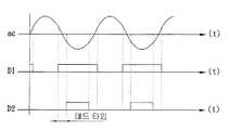
Translated fromKorean도 1 은 종래기술에 따라 부하를 구동하는 하프 브리지 인버터 회로의 개략적인 회로도;1 is a schematic circuit diagram of a half bridge inverter circuit for driving a load according to the prior art;
도 2 는 종래기술에 따른 하프 브리지 제어칩의 출력 제어신호 및 교류전원의 전압파형을 도시하는 개략적인 도면;2 is a schematic diagram showing an output control signal of a half bridge control chip and a voltage waveform of an AC power supply according to the prior art;
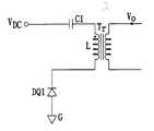
도 3 은 본 발명에 따라 부하를 구동하는 하프 브리지 인버터 회로의 개략적인 회로도;3 is a schematic circuit diagram of a half bridge inverter circuit for driving a load according to the present invention;
도 4a 내지 4f 는 본 발명에 따라 1 주기에서의 회로의 동작을 도시하는 개략적인 도면; 및4A-4F are schematic diagrams showing the operation of a circuit in one cycle in accordance with the present invention; And
도 5 는 본 발명에 따라 회로의 1 주기에서의 파형을 도시하는 개략적인 도면이다.5 is a schematic diagram illustrating waveforms in one cycle of a circuit in accordance with the present invention.
본 발명은 하프 브리지 인버터에 관한 것으로, 특히 외부구동 스위치 및 자체구동 스위치를 스위칭하여 인버전을 행하는 하프 브리지 인버터에 관한 것이다.The present invention relates to a half-bridge inverter, and more particularly, to a half-bridge inverter for performing inversion by switching the external drive switch and the self-drive switch.
전자 및 컴퓨터 장치가 복잡해짐에 따라, 전원장치가 이전보다 더 중요해지 고 있다. 전원장치는 크게 2 종류, 즉 선형 타입과 스위칭 타입으로 구분될 수 있다. 스위칭 타입이 선형 타입보다 유리하므로, 대부분의 전원장치는 스위칭 타입이다.As electronic and computer devices become more complex, power supplies are becoming more important than ever. There are two main types of power supplies: linear and switching. Since the switching type is advantageous over the linear type, most power supplies are switching types.
박막 트랜지스터 (TFT) 패널의 백라이트용 전원은 전력변환을 위해 주로 DC-AC 인버터 회로를 사용하고 조명을 위해 냉음극 형광램프 (CCFL: cold cathode fluorescent lamp) 를 구동한다. 상이한 회로구성을 이용하여, 종래의 인버터 회로는 일반적으로 하프 브리지 인버터 회로, 풀 브리지 인버터 회로, 및 푸시-풀 인버터 회로로 구분되는데, 이들은 직류를 교류로 변환하는 인버터 회로들이다.The power supply for the backlight of the TFT panel mainly uses a DC-AC inverter circuit for power conversion and drives a cold cathode fluorescent lamp (CCFL) for illumination. Using different circuit configurations, conventional inverter circuits are generally divided into half bridge inverter circuits, full bridge inverter circuits, and push-pull inverter circuits, which are inverter circuits for converting direct current into alternating current.
미국특허 제 5,615,093 호는 하프 브리지 인버터 회로에 대해 개시하고 있다. 도 1 은 부하를 구동하는 하프 브리지 인버터 회로의 개략적인 회로도이다. 도 1 에서, 변압기 (T1) 는 회로를 1차 회로와 2차 회로로 분할하고, 피드백 네트워크 (30) 가 이들 두 회로 사이에 접속된다. 1차 회로는 직류 전원 (VDD), 2개의 전자 스위치 (Q1 및 Q2), 하프 브리지 제어칩 (10), 및 LCC 공진 네트워크 (40)를 포함하고, 2차 회로는 램프 부하 (20)를 포함한다. 도 1 과 함께 도 2 를 참조하면, 종래기술에 따른 하프 브리지 제어칩의 출력 제어신호 및 교류 전압파형이 개략적으로 도시되어 있다. 하프 브리지 제어칩 (10)은 2개의 출력단 (LFET1 및 LFET2) 를 사용하여 제어신호 (D1 및 D2) 를 출력하고, 제어신호 (D1 및 D2) 는 각각 2개의 전자 스위치 (Q1 및 Q2) 의 스위칭을 제어한다. 2개의 전자 스위치 (Q1 및 Q2) 를 스위칭함으로써, 직류 전원의 전력이 LCC 공진 네트워크 (40) 를 통해 변압기 (T1) 의 1차 권선으로 공급되어 AC 전원 (ac) 을 정의한다. AC 전원 (ac) 은 변압기 (T1) 에 전력을 공급하기 위해 제공되고, 변압기 (T1) 는 램프 부하 (20) 를 구동하기 위하여 2차 권선으로 AC 전력을 스텝업 (step up) 하고 변환한다.U.S. Patent 5,615,093 discloses a half bridge inverter circuit. 1 is a schematic circuit diagram of a half bridge inverter circuit for driving a load. In Fig. 1, transformer T1 divides the circuit into a primary circuit and a secondary circuit, and a
상기 설명에서, 미국특허 제 5,615,093 호에 개시된 하프 브리지 인버터 회로는 상기 전원 스위치 (Q1 및 Q2) 를 직접 구동하고 스위치 (Q1 및 Q2) 의 교류 접속을 제어하기 위하여 적어도 2개의 출력을 갖는 하프 브리지 제어칩 (10) 을 필요로 한다. 또한, 하프 브리지 제어칩 (10) 은 스위치를 교대로 온/오프함으로써 제 1 스위치 (Q1) 와 제 2 스위치 (Q2) 가 짧은 시간동안 교번하도록 제어할 필요가 있다. 따라서, 제 1 스위치 (Q1) 와 제 2 스위치 (Q2) 를 모두 파괴시킬 제 1 스위치 (Q1) 와 제 2 스위치 (Q2) 의 전기적 접속을 방지하기 위해 도 2 에 도시된 바와 같이 제어신호 (D1 및 D2) 에 대해 약간의 데드 타임 (dead time) 을 가질 필요가 있다.In the above description, the half bridge inverter circuit disclosed in US Pat. No. 5,615,093 has a half bridge control having at least two outputs for directly driving the power switches Q1 and Q2 and controlling the AC connection of the switches Q1 and Q2.
또한, 제어신호 (D1 및 D2) 는 램프 부하 (20) 의 전력요건에 따라 부하에 전력을 공급하기 위하여 신호주기를 변경하고 제 1 스위치 (Q1) 및 제 2 스위치 (Q2) 의 스위칭을 제어할 필요가 있다. 하프 브리지 제어칩 (10) 은 예컨대 너무 낮은 전압출력, 너무 높은 전압출력, 램프의 개방회로, 과열 등과 같은 부하단으로부터 피드백된 조건들에 따라 회로를 보호할 필요가 있다. 제어신호 (D1 및 D2) 의 출력은 회로보호기능을 달성하기 위하여 제 1 스위치 (Q1) 와 제 2 스위치 (Q2) 를 스위치 오프하도록 되어 있다.In addition, the control signals D1 and D2 change the signal period to supply power to the load according to the power requirements of the
상술한 바와 같이, 종래의 하프 브리지 인버터 회로는 하프 브리지 회로를 구동하는 2개의 구동신호를 갖는 하프 브리지 제어칩 (10) 이 있다. 한편, 변압기의 제 2 회로를 보호할 보호회로도 필요하다. 이러한 요건으로 인해 비용이 높아지고 제품 크기가 지나치게 커지는 문제점이 있다.As described above, the conventional half bridge inverter circuit has a half
본 발명의 목적은 PWM 집적회로를 이용하고 외부구동 스위치 및 자체구동 스위치를 스위칭함으로써 인버전을 수행하는 하프 브리지 인버터를 제공하는 것이다. 외부구동 스위치는 정방형파 신호에 의해 제어되고 DC 전원을 교류전원으로 변환하여 적어도 하나의 램프에 전력을 공급하기 위하여 자체구동 스위치와 함께 작동한다.It is an object of the present invention to provide a half-bridge inverter that performs inversion by using a PWM integrated circuit and switching external drive switches and self-drive switches. The external drive switch is controlled by a square wave signal and works in conjunction with a self-driven switch to convert DC power into AC power to power at least one lamp.
본 발명은 1차 권선, 2차 권선, 및 보조권선을 갖는 변압기를 포함한다. 이 변압기는 외부구동 스위치와 접속된다. 이 외부구동 스위치는 변압기의 1차 권선 및 접지에 접속되고 정방형파 신호에 의해 제어된다. 자체구동 스위치는 변압기의 1차 권선, 보조 권선, 및 직류전원에 접속되고 보조 권선의 출력전압에 의해 제어된다. 공진 커패시터는 2차 권선에 접속된다. 따라서, 본 발명은 정방형파 신호를 이용하여 외부구동 스위치의 스위칭을 제어하고 보조 권선의 출력전압을 이용하여 자체구동 스위치의 스위칭을 제어한다. 이 스위치들을 교대로 스위칭함으로써, 직류전원이 변압기의 1차 권선에 도입되는 한편, 변압기의 2차 권선에서 교류전압을 검출한다. 이 교류전압은 공진 커패시터를 통해 교류 전력으로 변환된다. 또한, 본 발명의 외부구동 스위치는 외부구동 스위치에 있는 2개의 출력 게이트 사이에 제 1 극성 커패시터 (또는 추가 커패시터) 및 제 1 인터페이스 다이오드 (또는 추가 다이오드)를 포함한다. 본 발명의 자체구동 스위치는 자체구동 스위치에 있는 2개의 출력 게이트 사이에 제 2 극성 커패시터 (또는 추가 커패시터) 및 제 2 인터페이스 다이오드 (또는 추가 다이오드)를 포함한다. 따라서, 정방형파 신호 및 보조 권선의 출력전압은 외부구동 스위치 및 자체구동 스위치의 스위칭을 각각 제어하여 DC 전원에 의해 극성 커패시터 (또는 추가 커패시터) 및 제 2 극성 커패시터 (또는 추가 커패시터)를 충방전한다. 이 충방전 전력은 변압기의 1차 권선에 공급되어 변압기의 2차 권선에서 교류전압을 검출하고 공진 커패시터에 의해 AC 전력으로 변환된다.The present invention includes a transformer having a primary winding, a secondary winding, and an auxiliary winding. The transformer is connected to an external drive switch. This externally driven switch is connected to the primary winding and ground of the transformer and controlled by a square wave signal. The self-driving switch is connected to the primary winding of the transformer, the auxiliary winding, and the direct current power source and controlled by the output voltage of the auxiliary winding. The resonant capacitor is connected to the secondary winding. Therefore, the present invention controls the switching of the external drive switch using a square wave signal and the switching of the self-drive switch using the output voltage of the auxiliary winding. By alternately switching these switches, a direct current power source is introduced into the primary winding of the transformer while detecting an alternating voltage in the secondary winding of the transformer. This AC voltage is converted into AC power through a resonant capacitor. In addition, the external drive switch of the present invention includes a first polar capacitor (or additional capacitor) and a first interface diode (or additional diode) between two output gates in the external drive switch. The self-drive switch of the present invention includes a second polar capacitor (or additional capacitor) and a second interface diode (or additional diode) between two output gates in the self-drive switch. Thus, the square wave signal and the output voltage of the auxiliary winding control the switching of the external drive switch and the self drive switch, respectively, to charge and discharge the polar capacitor (or additional capacitor) and the second polar capacitor (or additional capacitor) by the DC power supply. . This charge and discharge power is supplied to the primary winding of the transformer to detect an alternating voltage in the secondary winding of the transformer and converted to AC power by a resonant capacitor.
이하, 첨부 도면을 참조하여 본 발명의 태양 및 이점에 대해 상세히 설명하기로 한다.Hereinafter, with reference to the accompanying drawings will be described in detail the aspects and advantages of the present invention.
도 3 은 본 발명에 따른 하프 브리지 인버터의 개략적인 회로도이다. 본 발명의 하프 브리지 인버터는 DC 전원 (VDC) 을 적어도 하나의 냉음극 형광램프 (CCFL)의 사용을 위해 공급되는 AC 전력으로 변환하기 위해 정방형 신호 (SPWM) 에 의해 제어된다. 하프 브리지 인버터는 변압기 (Tr) 의 1차 권선 (Np), 2차 권선 (Ns), 및 보조 권선 (Na) 을 포함한다. 외부구동 스위치 (Q1) 는 1차 권선 (Np) 및 접지 (G) 에 접속되고 정방형파 신호 (SPWM) 에 의해 제어된다. 자체구동 스위치 (Q2) 는 1차 권선 (Np), 보조 권선 (Na), 및 직류전원 (VDC) 에 접속되고 보조 권선 (Na) 의 출력전압에 의해 제어된다. 공진 커패시터는 2차 권선 (Ns) 에 접속 된다.3 is a schematic circuit diagram of a half bridge inverter according to the present invention. The half bridge inverter of the present invention is controlled by a square signal (SPWM ) to convert a DC power source (VDC) into AC power supplied for use of at least one cold cathode fluorescent lamp (CCFL). The half bridge inverter comprises a primary winding Np, a secondary winding Ns, and an auxiliary winding Na of the transformer Tr. The external drive switch Q1 is connected to the primary winding Np and ground G and controlled by the square wave signal SPWM . The self-driving switch Q2 is connected to the primary winding Np, the auxiliary winding Na, and the direct current power source VDC and is controlled by the output voltage of the auxiliary winding Na. The resonant capacitor is connected to the secondary winding Ns.
정방형파 신호 (SPWM) 에 의해 제어되는 외부구동 스위치 (Q1) 의 스위칭과 보조 권선 (Na) 의 출력전압에 의해 제어되는 자체구동 스위치 (Q2) 의 스위칭을 이용하여, DC 전원 (VDC) 은 변압기 (Tr) 의 1차 권선 (Np) 에 도입되어 변압기 (Tr) 의 2차 권선 (Ns) 에서 교류전압이 검출되고, 공진 커패시터 (C3) 에 의해 AC 전력으로 변환된다.By using the switching of the external drive switch Q1 controlled by the square wave signal SPWM and the switching of the self-driven switch Q2 controlled by the output voltage of the auxiliary winding Na, the DC power supply VDC Introduced into the primary winding Np of the transformer Tr, an alternating voltage is detected in the secondary winding Ns of the transformer Tr, and converted into AC power by the resonant capacitor C3.
도 3 을 참조하면, 본 발명은 외부구동 스위치 (Q1) 가 전기적으로 접속될 때 제어단을 통해 흐르는 전류를 억제하고 외부구동 스위치 (Q1) 가 오프되고 있는 동안에 외부구동 스위치 (Q1) 를 오프하도록 가속하기 위한 외부구동 스위치 (Q1) 의 제어단에 접속된 고속 다이오드 (D1) 를 더 포함한다. 제 2 가속 다이오드 (D2) 는 자체구동 스위치 (Q2) 가 전기적으로 접속될 때 제어단을 통해 흐르는 전류를 억제하고 자체구동 스위치 (Q2) 가 오프되고 있는 동안에 자체구동 스위치 (Q2) 를 오프하도록 가속하기 위한 자체구동 스위치 (Q2) 의 제어단 및 보조권선 (Na) 에 접속된다. 여기에서, 외부구동 스위치 (Q1) 는 외부구동 스위치의 2개의 출력 게이트 사이에 위치한 제 1 극성 커패시터 (CQ1) (또는 추가 커패시터) 및 제 1 인터페이스 다이오드 (또는 추가 다이오드) 를 갖는 N-채널 전계효과 트랜지스터 (FET) 이다. 또한, 자체구동 스위치 (Q2) 는 자체구동 스위치의 2개의 출력 게이트 사이에 위치한 제 2 극성 커패시터 (CQ2) (또는 추가 커패시터) 및 제 2 인터페이스 다이오드 (또는 추가 다이오드) 를 갖는 N-채널 전계효과 트랜지스터 (FET) 이다.Referring to Fig. 3, the present invention is intended to suppress the current flowing through the control stage when the external drive switch Q1 is electrically connected and to turn off the external drive switch Q1 while the external drive switch Q1 is off. It further comprises a high speed diode D1 connected to the control stage of the external drive switch Q1 for accelerating. The second acceleration diode D2 accelerates to suppress the current flowing through the control stage when the self-drive switch Q2 is electrically connected and to turn off the self-drive switch Q2 while the self-drive switch Q2 is off. Connected to the control stage of the self-actuated switch Q2 and the auxiliary winding Na. Here, the external drive switch Q1 has an N-channel field effect with a first polar capacitor CQ1 (or additional capacitor) and a first interface diode (or additional diode) located between two output gates of the external drive switch. Transistor (FET). The self-drive switch Q2 also has an N-channel field effect transistor having a second polar capacitor CQ2 (or additional capacitor) and a second interface diode (or additional diode) located between the two output gates of the self-drive switch. (FET).
도 4a 내지 4f 는 본 발명에 따라 1 주기에서의 회로의 동작을 도시하는 개략적인 도면이며, 도 5 는 본 발명의 회로의 1 주기에서의 파형을 도시하는 개략적인 도면이다. I 기간 동안에, 정방형파 신호 (SPWM) 는 하이 (high) 상태이고, 그 시간에서 외부구동 스위치 (Q1) 는 정방형파 신호 (SPWM) 의 제어에 의해 ON 상태로 되며 자체구동 스위치 (Q2) 는 OFF 상태로 된다. 따라서, DC 전원 (VDC) 은 커패시터 (C1) 및 변압기 (Tr) 를 통해 외부구동 스위치 (Q1) 에 이르는 경로를 따라 제공되고, 전류는 변압기 (Tr) 에 저장되며, 양의 교류전압 (Vo) 은 변압기 (Tr) 의 2차 권선 (Ns) 에 의해 검출된다.4A-4F are schematic diagrams showing the operation of a circuit in one cycle according to the present invention, and FIG. 5 is a schematic diagram showing waveforms in one cycle of the circuit of the present invention. During the I period, the square wave signal SPWM is in a high state, at which time the external drive switch Q1 is turned ON by the control of the square wave signal SPWM and the self-drive switch Q2 Is turned off. Thus, the DC power supply VDC is provided along the path from the capacitor C1 and the transformer Tr to the external drive switch Q1, the current is stored in the transformer Tr, and the positive alternating voltage Vo Is detected by the secondary winding Ns of the transformer Tr.
II 기간 동안에, 정방형파 신호 (SPWM) 는 외부구동 스위치 (Q1) 의 제어에 의해 OFF 상태로 되고, 자체구동 스위치 (Q2) 는 여전히 OFF 상태에 있다. 이때, 자체구동 스위치 (Q2) 의 제 2 극성 커패시터 (CQ2) 혹은 추가 커패시터에 일시적으로 저장되어 있는 전력이 방전될 것이고, 변압기 (Tr) 에 저장된 전류는 외부구동 스위치 (Q1) 의 제 1 극성 커패시터 (CQ1) 혹은 추가 커패시터를 충전할 것이다. 따라서, 변압기 (Tr) 의 2차 권선 (Ns) 의 교류전압 (Vo) 은 저전압 상태에 있다.During the period II, the square wave signal SPWM is turned OFF by the control of the external drive switch Q1, and the self drive switch Q2 is still in the OFF state. At this time, the power temporarily stored in the second polarity capacitor CQ2 or the additional capacitor of the self-driving switch Q2 will be discharged, and the current stored in the transformer Tr is the first polarity capacitor of the external driving switch Q1. (CQ1) or an additional capacitor will be charged. Thus, the AC voltage Vo of the secondary winding Ns of the transformer Tr is in a low voltage state.
III 기간 동안에, 외부구동 스위치 (Q1) 와 자체구동 스위치 (Q2) 는 여전히 OFF 상태에 있다. 제 1 극성 커패시터 (CQ1) 혹은 추가 커패시터가 DC 전원 (VDC) 의 전압까지 충전되고 제 2 극성 커패시터 (CQ2) 혹은 추가 커패시터가 0 전압으로 방전될 때, 제 2 인터페이스 다이오드 (DQ2) 혹은 추가 다이오드는 ON 상태로 되고 자체구동 스위치 (Q2) 는 0 전압으로 스위칭된다. 따라서, 변압기 (Tr) 의 2차 권선 (Ns) 에 의해 검출된 교류전압은 음의 교류전압 (Vo) 상태에 있다.During the III period, the external drive switch Q1 and the self drive switch Q2 are still in the OFF state. When the first polarity capacitor CQ1 or the additional capacitor is charged to the voltage of the DC power supply VDC and the second polarity capacitor CQ2 or the additional capacitor is discharged to zero voltage, the second interface diode DQ2 or the additional diode is It is turned on and the self-acting switch Q2 is switched to zero voltage. Therefore, the AC voltage detected by the secondary winding Ns of the transformer Tr is in a negative AC voltage Vo state.
IV 기간 동안에, 자체구동 스위치 (Q2) 는 변압기 (Tr) 의 보조권선 (Na) 의 제어에 의해 ON 상태로 된다. 이때, 변압기 (Tr) 의 1차 권선 (Np) 를 통해 흐르는 전류의 방향은 반대로 되고, 에너지가 변압기 (Tr) 에서 축적될 것이다. 이 기간에, 변압기 (Tr) 의 2차 권선 (Ns) 에 의해 검출된 교류전압은 음의 교류전압 상태에 있다.During the IV period, the self-drive switch Q2 is turned ON by the control of the auxiliary winding Na of the transformer Tr. At this time, the direction of the current flowing through the primary winding Np of the transformer Tr is reversed, and energy will accumulate in the transformer Tr. In this period, the AC voltage detected by the secondary winding Ns of the transformer Tr is in a negative AC voltage state.
V 기간 동안에, 자체구동 스위치 (Q2) 는 OFF 상태로 스위칭되고, 외부구동 스위치 (Q1) 는 여전히 OFF 상태에 있다. 이때, 외부구동 스위치 (Q1) 에 있는 제 1 극성 커패시터 (CQ1) 혹은 추가 커패시터는 일시적으로 저장된 전력을 방전하고, 이 변압기에 저장된 전류는 자체구동 스위치 (Q2) 에 있는 제 2 극성 커패시터 (CQ2) 혹은 추가 커패시터를 충전할 것이다. 따라서, 변압기 (Tr) 의 2차 권선 (Ns) 에 의해 검출된 교류전압 (Vo) 은 상승하는 전압상태에 있다.During the V period, the self-drive switch Q2 is switched to the OFF state, and the external drive switch Q1 is still in the OFF state. At this time, the first polar capacitor CQ1 or the additional capacitor in the external drive switch Q1 temporarily discharges the stored power, and the current stored in the transformer is the second polar capacitor CQ2 in the self-drive switch Q2. Or will charge an additional capacitor. Thus, the AC voltage Vo detected by the secondary winding Ns of the transformer Tr is in a rising voltage state.
VI 기간 동안에, 제 2 극성 커패시터 (CQ2) 혹은 추가 커패시터가 DC 전원 (VDC) 의 전압까지 충전되고 제 1 극성 커패시터 (CQ1) 혹은 추가 커패시터가 0 전압으로 방전되면, 제 1 인터페이스 다이오드 (DQ1) 혹은 추가 다이오드는 ON 상태로 될 것이다. 이때, 외부구동 스위치 (Q1) 는 0 전압으로 스위칭된다. 따라서, 변압기 (Tr) 의 2차 권선 (Ns) 에 의해 검출된 교류전압은 양의 교류전압 (Vo) 상태에 있다.During the VI period, when the second polar capacitor CQ2 or the additional capacitor is charged up to the voltage of the DC power supply VDC and the first polar capacitor CQ1 or the additional capacitor is discharged to zero voltage, the first interface diode DQ1 or The additional diode will be turned on. At this time, the external drive switch Q1 is switched to zero voltage. Therefore, the AC voltage detected by the secondary winding Ns of the transformer Tr is in a positive AC voltage Vo state.
상기한 바와 같이, 회로의 동작은 VI 기간이 종류된 후에 I 기간으로 되돌아와서 1 주기를 완료한다. 이 회로의 주기에서 출력된 교류전압 (Vo) 의 파형은 공진 커패시터 (C3) 에 의해 AC 전력 Vac 로 변환된다.As described above, the operation of the circuit returns to the I period after the VI period is sorted to complete one cycle. The waveform of the AC voltage Vo output in the cycle of this circuit is converted into AC power Vac by the resonant capacitor C3.
본 발명에 대해 가장 실제적이며 바람직한 실시예인 것으로 간주되는 것에 관해 설명되었지만, 본 발명이 여기 개시된 실시예에 한정되지 않음은 물론이다. 본 발명은 다양한 변형예 및 유사한 구성을 포함하도록 가장 광범위한 해석에 따르는 첨부된 청구범위의 사상과 범위 내에 포함되는 다양한 변형예를 포함하도록 한다.Although what has been described as what is considered to be the most practical and preferred embodiment of the invention, it is a matter of course that the invention is not limited to the embodiment disclosed herein. The present invention is intended to cover various modifications that fall within the spirit and scope of the appended claims in accordance with the broadest interpretation so as to encompass various modifications and similar constructions.
본 발명은 앞의 회로의 주기에 따라 인버전을 달성할 수 있다. 또한, 본 발명은 하프 브리지 회로를 구동하기 위해 정방형 신호를 필요로 할 뿐이다. 변압기의 2차 권선에서 단락이나 다른 오작동이 발생하면, 자체구동 스위치 (Q2) 는 그 동작을 계속할 수 없다. 본 발명은 회로보호를 위해 추가의 주변회로를 필요로 하지 않고, 따라서 제조비용과 제품크기를 줄일 수 있다.The present invention can achieve inversion according to the cycle of the foregoing circuit. Also, the present invention only needs a square signal to drive the half bridge circuit. If a short circuit or other malfunction occurs in the secondary winding of the transformer, the self-actuating switch Q2 cannot continue its operation. The present invention does not require additional peripheral circuitry for circuit protection, thus reducing manufacturing costs and product size.
Claims (7)
Translated fromKoreanPriority Applications (1)
| Application Number | Priority Date | Filing Date | Title |
|---|---|---|---|
| KR1020050034098AKR20060111763A (en) | 2005-04-25 | 2005-04-25 | Half-Bridge Inverter |
Applications Claiming Priority (1)
| Application Number | Priority Date | Filing Date | Title |
|---|---|---|---|
| KR1020050034098AKR20060111763A (en) | 2005-04-25 | 2005-04-25 | Half-Bridge Inverter |
Publications (1)
| Publication Number | Publication Date |
|---|---|
| KR20060111763Atrue KR20060111763A (en) | 2006-10-30 |
Family
ID=37620226
Family Applications (1)
| Application Number | Title | Priority Date | Filing Date |
|---|---|---|---|
| KR1020050034098ACeasedKR20060111763A (en) | 2005-04-25 | 2005-04-25 | Half-Bridge Inverter |
Country Status (1)
| Country | Link |
|---|---|
| KR (1) | KR20060111763A (en) |
Citations (4)
| Publication number | Priority date | Publication date | Assignee | Title |
|---|---|---|---|---|
| JPS61147777A (en)* | 1984-12-19 | 1986-07-05 | Matsushita Electric Ind Co Ltd | switching power supply circuit |
| JPH01140594A (en)* | 1987-11-25 | 1989-06-01 | Toshiba Electric Equip Corp | Fluorescent lamp lighting device |
| US5563777A (en)* | 1994-04-25 | 1996-10-08 | Matsushita Electric Works, Ltd. | Inverter AC power supply |
| US5615093A (en)* | 1994-08-05 | 1997-03-25 | Linfinity Microelectronics | Current synchronous zero voltage switching resonant topology |
- 2005
- 2005-04-25KRKR1020050034098Apatent/KR20060111763A/ennot_activeCeased
Patent Citations (4)
| Publication number | Priority date | Publication date | Assignee | Title |
|---|---|---|---|---|
| JPS61147777A (en)* | 1984-12-19 | 1986-07-05 | Matsushita Electric Ind Co Ltd | switching power supply circuit |
| JPH01140594A (en)* | 1987-11-25 | 1989-06-01 | Toshiba Electric Equip Corp | Fluorescent lamp lighting device |
| US5563777A (en)* | 1994-04-25 | 1996-10-08 | Matsushita Electric Works, Ltd. | Inverter AC power supply |
| US5615093A (en)* | 1994-08-05 | 1997-03-25 | Linfinity Microelectronics | Current synchronous zero voltage switching resonant topology |
Similar Documents
| Publication | Publication Date | Title |
|---|---|---|
| US8242754B2 (en) | Resonant power converter with half bridge and full bridge operations and method for control thereof | |
| US6954364B2 (en) | Backlight inverter for liquid crystal display panel with self-protection function | |
| TWI384745B (en) | Gate driver apparatus for alternately driving a half- or a full-bridge | |
| US6188183B1 (en) | High intensity discharge lamp ballast | |
| TWI763527B (en) | Flyback converter power supply and control method thereof | |
| KR950007608A (en) | Zero Voltage Switching Control Device for Resonant Converter and Electronic Ballast Using the Same | |
| US20130154492A1 (en) | Improvements relating rectifier circuits | |
| US5973943A (en) | Non zero-voltage switching protection circuit | |
| KR20070110997A (en) | Switch drive device, half bridge converter using the same and driving method thereof | |
| US7466567B2 (en) | Half-bridge CCFL driving apparatus | |
| US7212418B1 (en) | Synchronous rectifier control circuit | |
| CN1394461A (en) | Electronic ballast employing startup transient voltage suppression circuit | |
| KR100985335B1 (en) | Half-Bridge DC-DC Converter with Asymmetric Pulse Width Modulation | |
| JP2005501499A (en) | Half bridge circuit | |
| KR20060111763A (en) | Half-Bridge Inverter | |
| US20070211498A1 (en) | Boost converter | |
| JP2008289319A (en) | Discharge tube power supply system and semiconductor integrated circuit | |
| US20030169000A1 (en) | Discharge lamp lighting circuit | |
| Kim et al. | A low-cost high-efficiency CCFL inverter with new capacitive sensing and control | |
| US20060256598A1 (en) | Inverter device | |
| JP7619840B2 (en) | Semiconductor drive circuit and power conversion device | |
| US7564673B2 (en) | Control circuit for converters | |
| CN1801593B (en) | Half-bridge type converter | |
| KR100651079B1 (en) | Half-bridge inverter circuit with zero voltage switching | |
| CN100421347C (en) | Semi-bridge type converter circuit for driving double N-MOS by using push-pull control chip |
Legal Events
| Date | Code | Title | Description |
|---|---|---|---|
| A201 | Request for examination | ||
| PA0109 | Patent application | Patent event code:PA01091R01D Comment text:Patent Application Patent event date:20050425 | |
| PA0201 | Request for examination | ||
| E902 | Notification of reason for refusal | ||
| PE0902 | Notice of grounds for rejection | Comment text:Notification of reason for refusal Patent event date:20061018 Patent event code:PE09021S01D | |
| PG1501 | Laying open of application | ||
| E601 | Decision to refuse application | ||
| PE0601 | Decision on rejection of patent | Patent event date:20070117 Comment text:Decision to Refuse Application Patent event code:PE06012S01D Patent event date:20061018 Comment text:Notification of reason for refusal Patent event code:PE06011S01I |