KR20060108932A - Display device with a built-in detector and its driving method - Google Patents
Display device with a built-in detector and its driving methodDownload PDFInfo
- Publication number
- KR20060108932A KR20060108932AKR1020050030680AKR20050030680AKR20060108932AKR 20060108932 AKR20060108932 AKR 20060108932AKR 1020050030680 AKR1020050030680 AKR 1020050030680AKR 20050030680 AKR20050030680 AKR 20050030680AKR 20060108932 AKR20060108932 AKR 20060108932A
- Authority
- KR
- South Korea
- Prior art keywords
- sensing
- signal
- period
- common voltage
- image scanning
- Prior art date
- Legal status (The legal status is an assumption and is not a legal conclusion. Google has not performed a legal analysis and makes no representation as to the accuracy of the status listed.)
- Withdrawn
Links
Images


Classifications
- G—PHYSICS
- G06—COMPUTING OR CALCULATING; COUNTING
- G06F—ELECTRIC DIGITAL DATA PROCESSING
- G06F3/00—Input arrangements for transferring data to be processed into a form capable of being handled by the computer; Output arrangements for transferring data from processing unit to output unit, e.g. interface arrangements
- G06F3/01—Input arrangements or combined input and output arrangements for interaction between user and computer
- G06F3/03—Arrangements for converting the position or the displacement of a member into a coded form
- G06F3/041—Digitisers, e.g. for touch screens or touch pads, characterised by the transducing means
- G06F3/0412—Digitisers structurally integrated in a display
- B—PERFORMING OPERATIONS; TRANSPORTING
- B23—MACHINE TOOLS; METAL-WORKING NOT OTHERWISE PROVIDED FOR
- B23P—METAL-WORKING NOT OTHERWISE PROVIDED FOR; COMBINED OPERATIONS; UNIVERSAL MACHINE TOOLS
- B23P15/00—Making specific metal objects by operations not covered by a single other subclass or a group in this subclass
- B—PERFORMING OPERATIONS; TRANSPORTING
- B23—MACHINE TOOLS; METAL-WORKING NOT OTHERWISE PROVIDED FOR
- B23P—METAL-WORKING NOT OTHERWISE PROVIDED FOR; COMBINED OPERATIONS; UNIVERSAL MACHINE TOOLS
- B23P13/00—Making metal objects by operations essentially involving machining but not covered by a single other subclass
- B23P13/02—Making metal objects by operations essentially involving machining but not covered by a single other subclass in which only the machining operations are important
- G—PHYSICS
- G02—OPTICS
- G02F—OPTICAL DEVICES OR ARRANGEMENTS FOR THE CONTROL OF LIGHT BY MODIFICATION OF THE OPTICAL PROPERTIES OF THE MEDIA OF THE ELEMENTS INVOLVED THEREIN; NON-LINEAR OPTICS; FREQUENCY-CHANGING OF LIGHT; OPTICAL LOGIC ELEMENTS; OPTICAL ANALOGUE/DIGITAL CONVERTERS
- G02F1/00—Devices or arrangements for the control of the intensity, colour, phase, polarisation or direction of light arriving from an independent light source, e.g. switching, gating or modulating; Non-linear optics
- G02F1/01—Devices or arrangements for the control of the intensity, colour, phase, polarisation or direction of light arriving from an independent light source, e.g. switching, gating or modulating; Non-linear optics for the control of the intensity, phase, polarisation or colour
- G02F1/13—Devices or arrangements for the control of the intensity, colour, phase, polarisation or direction of light arriving from an independent light source, e.g. switching, gating or modulating; Non-linear optics for the control of the intensity, phase, polarisation or colour based on liquid crystals, e.g. single liquid crystal display cells
- G02F1/133—Constructional arrangements; Operation of liquid crystal cells; Circuit arrangements
- G02F1/1333—Constructional arrangements; Manufacturing methods
- G02F1/13338—Input devices, e.g. touch panels
- G—PHYSICS
- G09—EDUCATION; CRYPTOGRAPHY; DISPLAY; ADVERTISING; SEALS
- G09G—ARRANGEMENTS OR CIRCUITS FOR CONTROL OF INDICATING DEVICES USING STATIC MEANS TO PRESENT VARIABLE INFORMATION
- G09G3/00—Control arrangements or circuits, of interest only in connection with visual indicators other than cathode-ray tubes
- G09G3/20—Control arrangements or circuits, of interest only in connection with visual indicators other than cathode-ray tubes for presentation of an assembly of a number of characters, e.g. a page, by composing the assembly by combination of individual elements arranged in a matrix no fixed position being assigned to or needed to be assigned to the individual characters or partial characters
- G09G3/34—Control arrangements or circuits, of interest only in connection with visual indicators other than cathode-ray tubes for presentation of an assembly of a number of characters, e.g. a page, by composing the assembly by combination of individual elements arranged in a matrix no fixed position being assigned to or needed to be assigned to the individual characters or partial characters by control of light from an independent source
- G09G3/36—Control arrangements or circuits, of interest only in connection with visual indicators other than cathode-ray tubes for presentation of an assembly of a number of characters, e.g. a page, by composing the assembly by combination of individual elements arranged in a matrix no fixed position being assigned to or needed to be assigned to the individual characters or partial characters by control of light from an independent source using liquid crystals
- G09G3/3611—Control of matrices with row and column drivers
- G09G3/3648—Control of matrices with row and column drivers using an active matrix
- E—FIXED CONSTRUCTIONS
- E06—DOORS, WINDOWS, SHUTTERS, OR ROLLER BLINDS IN GENERAL; LADDERS
- E06B—FIXED OR MOVABLE CLOSURES FOR OPENINGS IN BUILDINGS, VEHICLES, FENCES OR LIKE ENCLOSURES IN GENERAL, e.g. DOORS, WINDOWS, BLINDS, GATES
- E06B3/00—Window sashes, door leaves, or like elements for closing wall or like openings; Layout of fixed or moving closures, e.g. windows in wall or like openings; Features of rigidly-mounted outer frames relating to the mounting of wing frames
- E06B3/70—Door leaves
- E06B3/72—Door leaves consisting of frame and panels, e.g. of raised panel type
- E06B3/76—Door leaves consisting of frame and panels, e.g. of raised panel type with metal panels
- G—PHYSICS
- G06—COMPUTING OR CALCULATING; COUNTING
- G06F—ELECTRIC DIGITAL DATA PROCESSING
- G06F3/00—Input arrangements for transferring data to be processed into a form capable of being handled by the computer; Output arrangements for transferring data from processing unit to output unit, e.g. interface arrangements
- G06F3/01—Input arrangements or combined input and output arrangements for interaction between user and computer
- G06F3/03—Arrangements for converting the position or the displacement of a member into a coded form
- G06F3/041—Digitisers, e.g. for touch screens or touch pads, characterised by the transducing means
- G06F3/042—Digitisers, e.g. for touch screens or touch pads, characterised by the transducing means by opto-electronic means
- G—PHYSICS
- G06—COMPUTING OR CALCULATING; COUNTING
- G06F—ELECTRIC DIGITAL DATA PROCESSING
- G06F3/00—Input arrangements for transferring data to be processed into a form capable of being handled by the computer; Output arrangements for transferring data from processing unit to output unit, e.g. interface arrangements
- G06F3/01—Input arrangements or combined input and output arrangements for interaction between user and computer
- G06F3/03—Arrangements for converting the position or the displacement of a member into a coded form
- G06F3/041—Digitisers, e.g. for touch screens or touch pads, characterised by the transducing means
- G06F3/047—Digitisers, e.g. for touch screens or touch pads, characterised by the transducing means using sets of wires, e.g. crossed wires
- G—PHYSICS
- G09—EDUCATION; CRYPTOGRAPHY; DISPLAY; ADVERTISING; SEALS
- G09G—ARRANGEMENTS OR CIRCUITS FOR CONTROL OF INDICATING DEVICES USING STATIC MEANS TO PRESENT VARIABLE INFORMATION
- G09G2300/00—Aspects of the constitution of display devices
- G09G2300/04—Structural and physical details of display devices
- G09G2300/0421—Structural details of the set of electrodes
- G09G2300/0426—Layout of electrodes and connections
- G—PHYSICS
- G09—EDUCATION; CRYPTOGRAPHY; DISPLAY; ADVERTISING; SEALS
- G09G—ARRANGEMENTS OR CIRCUITS FOR CONTROL OF INDICATING DEVICES USING STATIC MEANS TO PRESENT VARIABLE INFORMATION
- G09G2310/00—Command of the display device
- G09G2310/08—Details of timing specific for flat panels, other than clock recovery
- G—PHYSICS
- G09—EDUCATION; CRYPTOGRAPHY; DISPLAY; ADVERTISING; SEALS
- G09G—ARRANGEMENTS OR CIRCUITS FOR CONTROL OF INDICATING DEVICES USING STATIC MEANS TO PRESENT VARIABLE INFORMATION
- G09G2320/00—Control of display operating conditions
- G09G2320/02—Improving the quality of display appearance
- G09G2320/029—Improving the quality of display appearance by monitoring one or more pixels in the display panel, e.g. by monitoring a fixed reference pixel
- G09G2320/0295—Improving the quality of display appearance by monitoring one or more pixels in the display panel, e.g. by monitoring a fixed reference pixel by monitoring each display pixel
- G—PHYSICS
- G09—EDUCATION; CRYPTOGRAPHY; DISPLAY; ADVERTISING; SEALS
- G09G—ARRANGEMENTS OR CIRCUITS FOR CONTROL OF INDICATING DEVICES USING STATIC MEANS TO PRESENT VARIABLE INFORMATION
- G09G3/00—Control arrangements or circuits, of interest only in connection with visual indicators other than cathode-ray tubes
- G09G3/20—Control arrangements or circuits, of interest only in connection with visual indicators other than cathode-ray tubes for presentation of an assembly of a number of characters, e.g. a page, by composing the assembly by combination of individual elements arranged in a matrix no fixed position being assigned to or needed to be assigned to the individual characters or partial characters
- G09G3/34—Control arrangements or circuits, of interest only in connection with visual indicators other than cathode-ray tubes for presentation of an assembly of a number of characters, e.g. a page, by composing the assembly by combination of individual elements arranged in a matrix no fixed position being assigned to or needed to be assigned to the individual characters or partial characters by control of light from an independent source
- G09G3/36—Control arrangements or circuits, of interest only in connection with visual indicators other than cathode-ray tubes for presentation of an assembly of a number of characters, e.g. a page, by composing the assembly by combination of individual elements arranged in a matrix no fixed position being assigned to or needed to be assigned to the individual characters or partial characters by control of light from an independent source using liquid crystals
- G09G3/3611—Control of matrices with row and column drivers
- G09G3/3648—Control of matrices with row and column drivers using an active matrix
- G09G3/3655—Details of drivers for counter electrodes, e.g. common electrodes for pixel capacitors or supplementary storage capacitors
Landscapes
- Engineering & Computer Science (AREA)
- Physics & Mathematics (AREA)
- General Physics & Mathematics (AREA)
- Theoretical Computer Science (AREA)
- General Engineering & Computer Science (AREA)
- Crystallography & Structural Chemistry (AREA)
- Chemical & Material Sciences (AREA)
- Nonlinear Science (AREA)
- Computer Hardware Design (AREA)
- Human Computer Interaction (AREA)
- Mathematical Physics (AREA)
- Mechanical Engineering (AREA)
- Optics & Photonics (AREA)
- Control Of Indicators Other Than Cathode Ray Tubes (AREA)
- Liquid Crystal (AREA)
- Position Input By Displaying (AREA)
- Liquid Crystal Display Device Control (AREA)
Abstract
Translated fromKoreanDescription
Translated fromKorean도 1은 본 발명의 실시예에 따른 액정 표시 장치의 블록도이다.1 is a block diagram of a liquid crystal display according to an exemplary embodiment of the present invention.
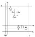
도 2는 본 발명의 한 실시예에 따른 액정 표시 장치의 광 감지부를 포함하는 화소에 대한 등가 회로도이다.2 is an equivalent circuit diagram of a pixel including a light detector of a liquid crystal display according to an exemplary embodiment of the present invention.
도 3은 본 발명의 한 실시예에 따른 액정 표시 장치의 접촉 감지부를 포함하는 화소에 대한 등가 회로도이다.3 is an equivalent circuit diagram of a pixel including a touch sensing unit of a liquid crystal display according to an exemplary embodiment of the present invention.
도 4는 본 발명의 한 실시예에 따른 액정 표시 장치의 개략도이다.4 is a schematic diagram of a liquid crystal display according to an exemplary embodiment of the present invention.
도 5는 본 발명의 한 실시예에 따른 액정 표시 장치에서의 각종 신호의 타이밍도이다.5 is a timing diagram of various signals in the liquid crystal display according to the exemplary embodiment of the present invention.
도 6은 본 발명의 한 실시예에 따른 액정 표시 장치의 액정 표시판 조립체, 영상 주사부 및 감지 주사부의 블록도이다.6 is a block diagram of a liquid crystal panel assembly, an image scanning unit, and a sensing scanning unit of a liquid crystal display according to an exemplary embodiment of the present invention.
도 7은 본 발명의 한 실시예에 따른 액정 표시 장치에서의 영상 주사부 및 감지 주사부의 입출력 신호를 도시한 타이밍도의 한 예이다.7 is an example of a timing diagram illustrating input and output signals of an image scanning unit and a sensing scanning unit in a liquid crystal display according to an exemplary embodiment of the present invention.
도 8은 본 발명의 한 실시예에 따른 액정 표시 장치에서의 영상 주사부 및 감지 주사부의 입출력 신호를 도시한 타이밍도의 다른 예이다.8 is another example of a timing diagram illustrating input and output signals of an image scanning unit and a sensing scanning unit in a liquid crystal display according to an exemplary embodiment of the present invention.
<도면 부호에 대한 설명><Description of Drawing>
31: 표시 영역32: 블랙 매트릭스31: display area 32: black matrix
33: 원 칩100, 200: 표시판33: One
300: 액정 표시판 조립체400: 영상 주사부300: liquid crystal panel assembly 400: image scanning unit
500: 데이터 구동부550: 계조 전압 생성부500: data driver 550: gray voltage generator
600: 신호 제어부700: 감지 주사부600: signal controller 700: detection scanning unit
800: 신호 판독부900: 공통 전압 생성부800: signal reader 900: common voltage generator
본 발명은 표시 장치 및 그 구동 방법에 관한 것으로서, 특히 감지부를 내장하는 표시 장치 및 그 구동 방법에 관한 것이다.BACKGROUND OF THE
일반적인 액정 표시 장치(liquid crystal display, LCD)는 화소 전극 및 공통 전극이 구비된 두 표시판과 그 사이에 들어 있는 유전율 이방성(dielectric anisotropy)을 갖는 액정층을 포함한다. 화소 전극은 행렬의 형태로 배열되어 있고 박막 트랜지스터(TFT) 등 스위칭 소자에 연결되어 한 행씩 차례로 데이터 전압을 인가 받는다. 공통 전극은 표시판의 전면에 걸쳐 형성되어 있으며 공통 전압을 인가 받는다. 화소 전극과 공통 전극 및 그 사이의 액정층은 회로적으로 볼 때 액정 축전기를 이루며, 액정 축전기는 이에 연결된 스위칭 소자와 함께 화소를 이루는 기본 단위가 된다.A typical liquid crystal display (LCD) includes two display panels provided with pixel electrodes and a common electrode, and a liquid crystal layer having dielectric anisotropy interposed therebetween. The pixel electrodes are arranged in a matrix and connected to switching elements such as thin film transistors (TFTs) to receive data voltages one by one in sequence. The common electrode is formed over the entire surface of the display panel and receives a common voltage. The pixel electrode, the common electrode, and the liquid crystal layer therebetween form a liquid crystal capacitor, and the liquid crystal capacitor becomes a basic unit that forms a pixel together with a switching element connected thereto.
이러한 액정 표시 장치에서는 두 전극에 전압을 인가하여 액정층에 전계를 생성하고, 이 전계의 세기를 조절하여 액정층을 통과하는 빛의 투과율을 조절함으로써 원하는 화상을 얻는다. 이때, 액정층에 한 방향의 전계가 오랫동안 인가됨으로써 발생하는 열화 현상을 방지하기 위하여 프레임별로, 행별로, 또는 화소별로 공통 전압에 대한 데이터 전압의 극성을 반전시킨다.In such a liquid crystal display, a voltage is applied to two electrodes to generate an electric field in the liquid crystal layer, and the intensity of the electric field is adjusted to adjust the transmittance of light passing through the liquid crystal layer to obtain a desired image. In this case, in order to prevent degradation caused by an electric field applied to the liquid crystal layer for a long time, the polarity of the data voltage with respect to the common voltage is inverted frame by frame, row by pixel, or pixel by pixel.
최근 이러한 액정 표시 장치에 접촉 센서 및/또는 광센서를 내장한 제품이 개발되어 왔다. 이들 센서는 사용자의 손 또는 터치 펜(touch pen) 등이 액정 표시 장치의 화면에 접촉하면 이에 따른 압력 및/또는 빛의 변화를 감지함으로써 사용자의 손가락 등이 화면에 접촉하였는지 여부 및 접촉 위치 정보를 검출할 수 있게 한다. 액정 표시 장치는 센서의 출력 신호인 감지 신호를 받아 적절히 처리하여 외부 장치로 전송하며, 외부 장치는 처리된 감지 신호로부터 접촉 여부 및 접촉 위치 등의 접촉 정보를 판단하여 이에 기초한 영상 신호를 액정 표시 장치에 전송한다.Recently, a product incorporating a contact sensor and / or an optical sensor has been developed in such a liquid crystal display. When the user's hand or touch pen touches the screen of the liquid crystal display, the sensor detects a change in pressure and / or light according to whether the user's finger touches the screen and the contact position information. To be detected. The liquid crystal display receives a sensing signal, which is an output signal of a sensor, appropriately processes and transmits the sensing signal to an external device. To transmit.
중소형 액정 표시 장치는 전력 소모를 줄이기 위하여 저전압 방식으로 데이터 전압을 구동하는데 극성 반전을 위하여 1 수평 주기마다 공통 전압의 레벨을 바꾼다. 그런데 감지 신호를 내보내는 배선은 공통 전극과 용량성으로 결합되어 있으므로 공통 전압이 변함에 따라 감지 신호가 영향을 받아 왜곡될 수 있다. 따라서 공통 전압이 변하지 않는 1 수평 주기 내에서 감지 신호를 읽어들일 필요가 있다. 그러나 해상도가 높아지면 1 수평 주기에 해당하는 시간이 짧아지고, 이에 따라 감지 신호를 읽는 시간도 짧아진다. 그러면 감지 신호의 크기가 작아지고 신호 대 잡음비(signal to noise ratio, SNR)도 작아진다. 결국 감지 신호는 잡음에 민 감하게 되어 접촉 정보를 판단하기 어렵게 된다.The small and medium size liquid crystal display drives a data voltage in a low voltage manner to reduce power consumption, and changes the level of the common voltage every one horizontal period for polarity inversion. However, since the wiring for emitting the detection signal is capacitively coupled with the common electrode, the detection signal may be affected and distorted as the common voltage changes. Therefore, it is necessary to read the sensing signal within one horizontal period in which the common voltage does not change. However, the higher the resolution, the shorter the time for one horizontal period, and thus the shorter the time for reading the sensed signal. This reduces the size of the sense signal and also reduces the signal to noise ratio (SNR). As a result, the sensed signal is sensitive to noise, making it difficult to determine contact information.
따라서 본 발명이 이루고자 하는 기술적 과제는 감지 신호를 충분한 시간 여유를 가지고 읽어들일 수 있으며 공통 전압으로 인한 왜곡을 최소화할 수 있는 감지부를 내장하는 표시 장치 및 그 구동 방법을 제공하는 것이다.Accordingly, an aspect of the present invention is to provide a display device and a method of driving the same, which include a sensing unit capable of reading a sensing signal with sufficient time margin and minimizing distortion caused by a common voltage.
이러한 기술적 과제를 이루기 위한 본 발명의 한 실시예에 따른 표시 장치는, 복수의 영상 주사선 및 복수의 감지 주사선을 포함하는 표시판, 상기 영상 주사선에 연결되어 있는 복수의 화소, 상기 감지 주사선에 연결되어 있으며, 외부로부터의 접촉에 따라 감지 신호를 출력하는 복수의 감지부, 상기 영상 주사선에 영상 주사 신호를 인가하는 영상 주사부, 상기 감지 주사선에 감지 주사 신호를 인가하는 감지 주사부, 그리고 한 프레임을 표시 구간과 감지 구간으로 나누어 상기 영상 주사부 및 상기 감지 주사부를 제어하는 신호 제어부를 포함한다.According to an embodiment of the present invention, a display device including a plurality of image scanning lines and a plurality of sensing scan lines, a plurality of pixels connected to the image scanning line, and a sensing scan line are connected. A plurality of detectors for outputting a sensing signal according to a contact from an outside, an image scanning unit for applying an image scanning signal to the image scanning line, a sensing scanning unit for applying a sensing scanning signal to the sensing scanning line, and one frame And a signal controller configured to control the image scanning unit and the detection scanning unit by dividing the interval into the detection interval.
상기 영상 주사부는 상기 표시 구간에서 상기 영상 주사 신호를 인가하고, 상기 감지 주사부는 상기 감지 구간에서 상기 감지 주사 신호를 인가할 수 있다.The image scanning unit may apply the image scanning signal in the display section, and the detection scanning unit may apply the sensing scan signal in the sensing section.
상기 화소에 인가되는 공통 전압은 하이 레벨과 로우 레벨 사이를 스윙할 수 있다.The common voltage applied to the pixel may swing between a high level and a low level.
상기 공통 전압은 상기 표시 구간에서 제1 주기를 가지고 상기 감지 구간에서 제2 주기를 가질 수 있다.The common voltage may have a first period in the display period and a second period in the sensing period.
상기 공통 전압의 상기 제1 및 제2 주기는 서로 다를 수 있다.The first and second periods of the common voltage may be different from each other.
상기 공통 전압의 상기 제1 주기는 상기 제2 주기보다 짧을 수 있다.The first period of the common voltage may be shorter than the second period.
상기 제1 주기를 가지는 상기 공통 전압의 제1 듀티비와 상기 제2 주기를 가지는 상기 공통 전압의 제2 듀티비는 서로 다를 수 있다.The first duty ratio of the common voltage having the first period and the second duty ratio of the common voltage having the second period may be different from each other.
상기 공통 전압의 제1 듀티비는 실질적으로 50%일 수 있다.The first duty ratio of the common voltage may be substantially 50%.
상기 감지 주사 신호는 상기 공통 전압이 상기 하이 및 로우 레벨 중 어느 한 레벨인 경우에 출력될 수 있다.The sensing scan signal may be output when the common voltage is one of the high and low levels.
상기 공통 전압이 상기 하이 및 로우 레벨 중 어느 한 레벨인 경우에 상기 감지 신호를 읽어들이는 신호 판독부를 더 포함할 수 있다.The display apparatus may further include a signal reading unit configured to read the sensing signal when the common voltage is one of the high and low levels.
상기 공통 전압의 상기 하이 및 로우 레벨 중 시간이 긴 레벨에서 상기 감지 신호를 읽어들이는 신호 판독부를 더 포함할 수 있다.The apparatus may further include a signal reading unit configured to read the sensing signal at a long time level among the high and low levels of the common voltage.
상기 화소에 인가되는 공통 전압은 상기 표시 구간에서 하이 레벨과 로우 레벨 사이를 스윙하고 상기 감지 구간에서 직류 전압일 수 있다.The common voltage applied to the pixel may swing between a high level and a low level in the display period and may be a DC voltage in the detection period.
본 발명의 다른 태양에 따른 표시 장치는, 복수의 영상 주사선 및 복수의 감지 주사선을 포함하는 표시판, 상기 영상 주사선에 연결되어 있는 복수의 화소, 상기 감지 주사선에 연결되어 있으며, 외부로부터의 접촉에 따라 감지 신호를 출력하는 복수의 감지부, 상기 영상 주사선에 영상 주사 신호를 인가하는 영상 주사부, 상기 감지 주사선에 감지 주사 신호를 인가하는 감지 주사부, 한 프레임 내에서 서로 다른 제1 및 제2 주기를 가지는 공통 전압을 생성하여 상기 표시판에 인가하는 공통 전압 생성부, 그리고 상기 영상 주사부, 상기 감지 주사부 및 상기 공통 전압 생성부를 제어하는 신호 제어부를 포함한다.According to another aspect of the present invention, a display device includes a display panel including a plurality of image scanning lines and a plurality of sensing scan lines, a plurality of pixels connected to the image scanning line, and connected to the sensing scan line, A plurality of sensing units for outputting a sensing signal, an image scanning unit for applying an image scanning signal to the image scanning line, a sensing scanning unit for applying a sensing scanning signal to the sensing scanning line, and different first and second periods in one frame And a signal controller configured to generate a common voltage having a voltage applied to the display panel, and to control the image scan unit, the sensing scan unit, and the common voltage generator.
상기 영상 주사부는 상기 공통 전압이 상기 제1 주기를 가질 때 상기 영상 주사 신호를 인가하고, 상기 감지 주사부는 상기 공통 전압이 상기 제2 주기를 가질 때 상기 감지 주사 신호를 인가할 수 있다.The image scanning unit may apply the image scanning signal when the common voltage has the first period, and the sensing scan unit may apply the sensing scan signal when the common voltage has the second period.
상기 공통 전압의 상기 제1 주기는 상기 제2 주기보다 짧을 수 있다.The first period of the common voltage may be shorter than the second period.
상기 제2 주기를 가지는 공통 전압은 길이가 서로 다른 하이 레벨과 로우 레벨을 가질 수 있다.The common voltage having the second period may have a high level and a low level having different lengths.
상기 공통 전압의 상기 하이 레벨 및 로우 레벨 중 길이가 긴 레벨에서 상기 감지 신호를 읽어들일 수 있다.The sensing signal may be read at a length longer than the high level and the low level of the common voltage.
본 발명의 다른 태양에 따른, 복수의 영상 주사선, 복수의 감지 주사선, 상기 영상 주사선에 연결되어 있는 복수의 화소, 상기 감지 주사선에 연결되어 있으며 외부로부터의 접촉에 따라 감지 신호를 출력하는 복수의 감지부를 포함하는 표시 장치의 구동 방법은, 한 프레임을 표시 구간과 감지 구간으로 나누는 단계, 상기 표시 구간에서 영상 주사 신호를 인가하는 단계, 그리고 상기 감지 구간에서 감지 주사 신호를 인가하는 단계를 포함한다.According to another aspect of the present invention, a plurality of image scanning lines, a plurality of sensing scan lines, a plurality of pixels connected to the image scanning line, a plurality of sensing connected to the sensing scanning line and outputting a sensing signal according to a contact from outside A driving method of a display device including a unit includes dividing a frame into a display section and a sensing section, applying an image scan signal in the display section, and applying a sensing scan signal in the sensing section.
상기 표시 구간에서 제1 주기를 가지고 상기 감지 구간에서 상기 제1 주기와 서로 다른 제2 주기를 가지는 공통 전압을 인가하는 단계를 더 포함할 수 있다.The method may further include applying a common voltage having a first period in the display period and a second period different from the first period in the sensing period.
상기 제2 주기를 가지는 공통 전압은 길이가 서로 다른 하이 레벨과 로우 레벨을 가질 수 있다.The common voltage having the second period may have a high level and a low level having different lengths.
상기 공통 전압의 상기 하이 레벨 및 로우 레벨 중 길이가 긴 레벨에서 상기 감지 신호를 읽어들이는 단계를 더 포함할 수 있다.The method may further include reading the sensing signal at a long level of the high level and the low level of the common voltage.
첨부한 도면을 참고로 하여 본 발명의 실시예에 대하여 본 발명이 속하는 기술 분야에서 통상의 지식을 가진 자가 용이하게 실시할 수 있도록 상세히 설명한다.DETAILED DESCRIPTION Embodiments of the present invention will be described in detail with reference to the accompanying drawings so that those skilled in the art may easily implement the present invention.
도면에서 여러 층 및 영역을 명확하게 표현하기 위하여 두께를 확대하여 나타내었다. 명세서 전체를 통하여 유사한 부분에 대해서는 동일한 도면 부호를 붙였다. 층, 막, 영역, 판 등의 부분이 다른 부분 "위에" 있다고 할 때, 이는 다른 부분 "바로 위에" 있는 경우뿐 아니라 그 중간에 또 다른 부분이 있는 경우도 포함한다. 반대로 어떤 부분이 다른 부분 "바로 위에" 있다고 할 때에는 중간에 다른 부분이 없는 것을 뜻한다.In the drawings, the thickness of layers, films, panels, regions, etc., are exaggerated for clarity. Like parts are designated by like reference numerals throughout the specification. When a part of a layer, film, region, plate, etc. is said to be "on" another part, this includes not only the other part being "right over" but also another part in the middle. On the contrary, when a part is "just above" another part, there is no other part in the middle.
이제 본 발명의 실시예에 따른 감지부를 내장하는 표시 장치 및 그 구동 방법에 대하여 도면을 참고로 하여 상세하게 설명한다.Now, a display device including a sensing unit and a driving method thereof according to an exemplary embodiment of the present invention will be described in detail with reference to the accompanying drawings.
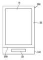
도 1은 본 발명의 실시예에 따른 액정 표시 장치의 블록도이고, 도 2는 본 발명의 한 실시예에 따른 액정 표시 장치의 광 감지부를 포함하는 화소에 대한 등가 회로도이며, 도 3은 본 발명의 한 실시예에 따른 액정 표시 장치의 접촉 감지부를 포함하는 화소에 대한 등가 회로도이다. 도 4는 본 발명의 한 실시예에 따른 액정 표시 장치의 개략도이다.1 is a block diagram of a liquid crystal display according to an exemplary embodiment of the present invention, FIG. 2 is an equivalent circuit diagram of a pixel including a light sensing unit of the liquid crystal display according to an exemplary embodiment of the present invention, and FIG. An equivalent circuit diagram of a pixel including a touch sensing unit of a liquid crystal display according to an exemplary embodiment is shown. 4 is a schematic diagram of a liquid crystal display according to an exemplary embodiment of the present invention.
도 1에 도시한 바와 같이, 본 발명의 한 실시예에 따른 액정 표시 장치는 액정 표시판 조립체(liquid crystal panel assembly)(300) 및 이에 연결된 영상 주사부(400), 데이터 구동부(500), 감지 주사부(700), 신호 판독부(800), 공통 전압 생성부(900), 데이터 구동부(500)에 연결된 계조 전압 생성부(550), 그리고 이들을 제어하는 신호 제어부(600)를 포함한다.As shown in FIG. 1, a liquid crystal display according to an exemplary embodiment of the present invention includes a liquid
액정 표시판 조립체(300)는 등가 회로로 볼 때 복수의 신호선(G1-Gn, D1-Dm, S1-Sn, P1-Pm, Psg, Psd)과 이에 연결되어 있으며 대략 행렬의 형태로 배열된 복수의 화소(pixel)를 포함한다.The liquid
신호선(G1-Gn, D1-Dm)은 영상 주사 신호(Vg1-Vgn)를 전달하는 복수의 영상 주사선(G1-Gn)과 영상 데이터 신호를 전달하는 데이터선(D1-Dm)을 포함한다. 영상 주사선(G1-Gn)은 대략 행 방향으로 뻗어 있으며 서로가 거의 평행하고 데이터선(D1-Dm)은 대략 열 방향으로 뻗어 있으며 서로가 거의 평행하다.Signal lines(G 1 -G n, D 1 -D m) is data for transmitting a plurality of video scan lines (G1 -Gn) and the image data signal carrying the image scan signal (Vg1 -Vgn) line (D1 -Dm ). The image scanning lines G1 -Gn extend substantially in the row direction and are substantially parallel to each other, and the data lines D1 -Dm extend substantially in the column direction and are substantially parallel to each other.
신호선(S1-Sn, P1-Pm)은 감지 주사 신호(Vs1-Vsn)를 전달하는 복수의 감지 주사선(S1-Sn)과 감지 신호를 전달하는 감지 신호선(P1-Pm)을 포함한다. 감지 주사선(S1-Sn)은 대략 행 방향으로 뻗어 있으며 서로가 거의 평행하고 감지 신호선(P1-Pm)은 대략 열 방향으로 뻗어 있으며 서로가 거의 평행하다.The signal lines S1 -Sn and P1 -Pm are a plurality of sensing scan lines S1 -Sn transmitting the sensing scan signals Vs1 -Vsn and a sensing signal line P1 transferring the sensing signals. -Pm ). The sensing scan lines S1 -Sn extend substantially in the row direction and are substantially parallel to each other, and the sensing signal lines P1 -Pm extend substantially in the column direction and are substantially parallel to each other.
신호선(Psg, Psd)은 제어 전압(Vsg)을 전달하는 제어 전압선(Psg)과 입력 전압(Vsd)을 전달하는 입력 전압선(Psd)을 포함한다.The signal lines Psg and Psd include a control voltage line Psg for transmitting the control voltage Vsg and an input voltage line Psd for transferring the input voltage Vsd.
각 화소는 신호선(G1-Gn, D1-Dm)에 연결된 스위칭 소자(Qs1)와 이에 연결된 액정 축전기(liquid crystal capacitor)(CLC) 및 유지 축전기(storage capacitor)(CST)를 포함한다. 유지 축전기(CST)는 필요에 따라 생략할 수 있다.Each pixel includes a switching element Qs1 connected to a signal line G1 -Gn , D1 -Dm , a liquid crystal capacitor CLC , and a storage capacitor CST connected thereto. Include. The holding capacitor CST can be omitted as necessary.
박막 트랜지스터 등 스위칭 소자(Qs1)는 삼단자 소자로서 그 제어 단자 및 입력 단자는 각각 영상 주사선(G1-Gn) 및 데이터선(D1-Dm)에 연결되어 있으며, 출력 단자는 액정 축전기(CLC) 및 유지 축전기(CST)에 연결되어 있다.The switching element Qs1 such as a thin film transistor is a three-terminal element whose control terminal and input terminal are connected to the image scanning line G1 -Gn and the data line D1 -Dm, respectively, and the output terminal is a liquid crystal capacitor. (CLC ) and holding capacitor (CST ).
액정 축전기(CLC)는 액정 표시판 조립체(300)의 하부 표시판(100)의 화소 전극(도시하지 않음)과 상부 표시판(200)의 공통 전극(도시하지 않음)을 두 단자로 하며 두 전극 사이의 액정층은 유전체로서 기능한다. 화소 전극은 스위칭 소자(Qs1)에 연결되며 공통 전극은 상부 표시판(200)의 전면에 형성되어 있고 공통 전압(Vcom)을 인가받는다.The liquid crystal capacitor CLC has two terminals, a pixel electrode (not shown) of the
액정 축전기(CLC)의 보조적인 역할을 하는 유지 축전기(CST)는 하부 표시판(100)에 구비된 별개의 신호선(도시하지 않음)과 화소 전극이 절연체를 사이에 두고 중첩되어 이루어지며 이 별개의 신호선에는 공통 전압(Vcom) 따위의 정해진 전압이 인가된다. 그러나 유지 축전기(CST)는 화소 전극이 절연체를 매개로 바로 위의 전단 게이트선과 중첩되어 이루어질 수 있다.The storage capacitor CST , which serves as an auxiliary part of the liquid crystal capacitor CLC , is formed by overlapping a separate signal line (not shown) and a pixel electrode of the
한편, 색 표시를 구현하기 위해서는 각 화소가 원색(primary color) 중 하나를 고유하게 표시하거나(공간 분할) 각 화소가 시간에 따라 번갈아 원색을 표시하게(시간 분할) 하여 이들 원색의 공간적, 시간적 합으로 원하는 색상이 인식되도록 한다. 원색의 예로는 적색, 녹색 및 청색을 들 수 있다.On the other hand, in order to implement color display, each pixel uniquely displays one of the primary colors (spatial division) or each pixel alternately displays the primary colors according to time (time division) so that the spatial and temporal combination of these primary colors can be achieved. To recognize the desired color. Examples of primary colors include red, green and blue.
도 2에 도시한 바와 같이 화소는 광 감지부를 포함하는데, 이는 신호선(Psg, Psd)에 연결된 광 감지 소자(Qp), 신호선(S1-Sn, P1-Pm)에 연결된 스위칭 소자(Qs2)와 이들에 연결된 감지 신호 축전기(Cp)를 포함한다. 그러나 모든 화소가 이러한 광 감지부를 포함할 필요는 없고 광 감지부의 해상도는 필요에 따라 조정될 수 있다. 즉, 복수의 화소 중 하나의 화소가 광 감지부를 포함할 수 있으며, 액정 표시판 조립체(300)에서 소정 간격마다 광 감지부를 배치할 수 있다. 이에 따라 감지 주사선(S1-Sn) 및 감지 신호선(P1-Pm)의 수효도 조정될 수 있다.As shown in FIG. 2, the pixel includes a light sensing unit, which includes a light sensing element Qp connected to signal lines Psg and Psd, and a switching element connected to signal lines S1 -Sn and P1 -Pm . Qs2) and sense signal capacitors Cp connected thereto. However, not all pixels need to include such a light detector, and the resolution of the light detector may be adjusted as needed. That is, one pixel of the plurality of pixels may include a light sensing unit, and the light sensing unit may be disposed at predetermined intervals in the liquid
예를 들어 액정 표시 장치의 해상도가 QVGA(quarter video graphics array, 240*320 도트)인 경우, 광 감지부의 해상도가 QVGA이면 3개의 화소 당 하나의 광 감지부가 배치되며, 광 감지부의 해상도가 QQVGA(quarter QVGA, 120*160 도트)이면 12개의 화소 당 하나의 광 감지부가 배치된다. 여기서 1 도트는 3개의 화소가 모여 하나의 영상을 표시하는 단위를 의미한다.For example, when the resolution of the liquid crystal display device is a quarter video graphics array (QVGA) of 240 * 320 dots, if the resolution of the light detector is QVGA, one light detector is disposed per three pixels, and the resolution of the light detector is QQVGA ( quarter QVGA (120 * 160 dots), one light sensor is disposed per 12 pixels. Here, one dot means a unit in which three pixels are collected to display one image.
광 감지 소자(Qp)는 삼단자 소자로서 그 제어 단자 및 입력 단자는 각각 제어 전압선(Psg)과 입력 전압선(Psd)에 연결되어 있으며, 출력 단자는 감지 신호 축전기(Cp) 및 스위칭 소자(Qs2)에 연결되어 있다. 광 감지 소자(Qp)는 그 채널부 반도체에 빛이 조사되면 비정질 규소(amorphous silicon) 또는 다결정 규소(poly crystalline silicon)로 이루어진 채널부 반도체가 광전류를 형성하고, 입력 전압선(Psd)에 인가된 입력 전압(Vsd)에 의해 광전류가 감지 신호 축전기(Cp) 및 스위칭 소자(Qs2) 방향으로 흐른다.The photosensitive element Qp is a three-terminal element whose control terminal and input terminal are connected to the control voltage line Psg and the input voltage line Psd, respectively, and the output terminal is the sensing signal capacitor Cp and the switching element Qs2. Is connected to. When the light sensing element Qp is irradiated with light to the channel semiconductor, a channel semiconductor made of amorphous silicon or poly crystalline silicon forms a photocurrent, and an input applied to the input voltage line Psd. The photocurrent flows in the direction of the sensing signal capacitor Cp and the switching element Qs2 by the voltage Vsd.
감지 신호 축전기(Cp)는 광 감지 소자(Qp)와 제어 전압선(Psg) 사이에 연결 되어 있고, 광 감지 소자(Qp)로부터의 광전류에 따른 전하를 축적하여 소정 전압을 유지한다. 감지 신호 축전기(Cp)는 필요에 따라 생략할 수 있다.The sensing signal capacitor Cp is connected between the photosensitive device Qp and the control voltage line Psg, and accumulates charges according to the photocurrent from the photosensitive device Qp to maintain a predetermined voltage. The sensing signal capacitor Cp may be omitted as necessary.
스위칭 소자(Qs2) 역시 삼단자 소자로서 그 제어 단자, 출력 단자 및 입력 단자는 각각 감지 주사선(S1-Sn), 감지 신호선(P1-Pm) 및 광 감지 소자(Qp)에 연결되어 있다. 스위칭 소자(Qs2)는 감지 주사선(S1-Sn)에 스위칭 소자(Q)를 턴 온시키는 전압이 인가되면 감지 신호 축전기(Cp)에 저장되어 있는 전압 또는 광 감지 소자(Qp)로부터의 광전류를 광 감지 신호(Vp)로서 감지 신호선(P1-Pm)으로 출력한다.The switching element Qs2 is also a three-terminal element whose control terminal, output terminal and input terminal are connected to the sensing scan lines S1 -Sn , the sensing signal lines P1 -Pm and the photo sensing element Qp, respectively. have. The switching element Qs2 is a voltage stored in the sensing signal capacitor Cp or a photocurrent from the photosensitive element Qp when a voltage for turning on the switching element Q is applied to the sensing scan lines S1 -Sn . Is output as the sensing signal line Vp to the sensing signal lines P1 -Pm .
한편 도 3에 도시한 바와 같이 일부의 화소는 접촉 감지부를 포함한다. 접촉 감지부는 공통 전압(Vcom)에 연결되어 있는 스위치(SWT), 스위치(SWT)와 신호선(Psg)에 연결된 접촉 감지 소자(Qt) 및 신호선(S1-Sn, P1-Pm) 중 일부에 연결된 스위칭 소자(Qs3)를 포함한다.Meanwhile, as shown in FIG. 3, some pixels include a touch sensing unit. The touch sensing unit may include a switch SWT connected to the common voltage Vcom, a touch sensing element Qt connected to the switch SWT and the signal line Psg, and a signal line S1 -Sn , P1 -Pm . It includes a switching element Qs3 connected to some.
접촉 감지부는 신호선(S1-Sn, P1-Pm)이 교차하는 화소 중 광 감지부를 포함하지 않는 화소에 포함되어 있으며, 접촉 감지부의 해상도는 필요에 따라 조정될 수 있다.The touch sensing unit is included in a pixel not including the light sensing unit among the pixelswhere the signal lines S1 -Sn and P1 -Pm cross each other, and the resolution of the touch sensing unit may be adjusted as necessary.
스위치(SWT)는 사용자의 접촉에 따라 공통 전압(Vcom)을 접촉 감지 소자(Qt)에 전달한다.The switch SWT transfers the common voltage Vcom to the touch sensing element Qt according to the user's touch.
접촉 감지 소자(Qt)는 삼단자 소자로서 그 제어 단자 및 입력 단자는 각각 제어 전압선(Psg)과 스위치(SWT)에 연결되어 있으며, 출력 단자는 스위칭 소자 (Qs3)에 연결되어 있다. 접촉 감지 소자(Qt)는 스위치(SWT)로부터 전달된 공통 전압(Vcom)에 따른 누설 전류를 출력한다.The touch sensing element Qt is a three-terminal element whose control terminal and input terminal are connected to the control voltage line Psg and the switch SWT, respectively, and the output terminal is connected to the switching element Qs3. The touch sensing element Qt outputs a leakage current according to the common voltage Vcom transferred from the switch SWT.
스위칭 소자(Qs3) 역시 삼단자 소자로서 그 제어 단자, 출력 단자 및 입력 단자는 각각 감지 주사선(S1-Sn), 감지 신호선(P1-Pm) 및 접촉 감지 소자(Qt)에 연결되어 있다. 스위칭 소자(Qs3)는 감지 주사선(S1-Sn)에 스위칭 소자(Qs3)를 턴 온시키는 전압이 인가되면 접촉 감지 소자(Qt)로부터의 누설 전류를 접촉 감지 신호(Vt)로서 해당 감지 신호선(P1-Pm)으로 출력한다.The switching element Qs3 is also a three-terminal element whose control terminal, output terminal and input terminal are connected to the sensing scan lines S1 -Sn , the sensing signal lines P1 -Pm and the touch sensing element Qt, respectively. have. The switching element Qs3 uses the leakage current from the touch sensing element Qt as the touch sensing signal Vt when the voltage for turning on the switching element Qs3 is applied to the sensing scan lines S1 -Sn . Output as (P1 -Pm ).
하나의 감지 신호선(P1-Pm)에 광 감지부 및 접촉 감지부가 함께 연결될 수도 있으나, 광 감지부 및 접촉 감지부 중 어느 하나만 연결되는 것이 바람직하다.The light sensing unit and the touch sensing unit may be connected together to one sensing signal line P1 -Pm , but only one of the light sensing unit and the touch sensing unit is connected.
여기서 스위칭 소자(Qs1, Qs2, Qs3), 감지 소자(Qp, Qt)는 비정질 규소 또는 다결정 규소 박막 트랜지스터로 이루어질 수 있다.The switching elements Qs1, Qs2, and Qs3 and the sensing elements Qp and Qt may be formed of amorphous silicon or polycrystalline silicon thin film transistors.
광 감지부는 사용자가 접촉한 부분에만 그림자가 드리워져 접촉된 위치를 감지할 수 있으나, 접촉 감지부는 사용자의 접촉(압력)에 의하여 유리 등으로 이루어진 액정 표시판 조립체(300)가 넓은 면적에 걸쳐 눌리므로 복수의 스위치(SWT)가 접촉하게 되어 접촉된 위치를 감지하기 어렵고 단지 접촉 여부만을 감지할 수 있다.The light detector may detect a position where a shadow is cast only on a portion where the user touches, but the touch detector is pressed by a user's contact (pressure) over the large area because the liquid
감지부의 해상도가 낮으면 감지 신호를 처리하는 시간을 줄일 수 있으므로 가능한 한 감지부의 해상도를 낮추는 것이 바람직하다. 특히 접촉 감지부의 해상도가 광 감지부의 해상도보다 낮을 수도 있으며 그렇더라도 접촉 여부를 판단하는 데 큰 영향을 미치지 않는다.If the resolution of the detector is low, it may reduce the processing time of the detection signal, so it is desirable to reduce the resolution of the detector as much as possible. In particular, the resolution of the touch sensing unit may be lower than the resolution of the light sensing unit, but it does not affect the determination of the contact.
한편 광 감지부 및 접촉 감지부가 화소에 포함되어 있는 것으로 설명하였으나 이들 감지부는 화소 사이 또는 화소 밖의 별도의 영역에 배치될 수도 있다.Meanwhile, although the light sensing unit and the touch sensing unit are described as being included in the pixels, the sensing units may be disposed in separate areas between or outside the pixels.
도 4에 도시한 바와 같이, 액정 표시판 조립체(300)는 표시 영역(31)을 정의하는 블랙 매트릭스(32)를 포함하며, 화소와 신호선(G1-Gn, D1-Dm, S1-Sn, P1-Pm, Psg, Psd)의 대부분은 표시 영역(31) 내에 위치한다. 상부 표시판(200)은 하부 표시판(100)보다 크기가 작아서 하부 표시판(100)의 일부 영역이 노출되며, 데이터선(D1-Dm)은 이 영역에까지 연장되어 데이터 구동부(500)와 연결된다. 주사선(G1-Gn, S1-Sn)은 또한 블랙 매트릭스(32)로 가려진 영역으로 연장되어 영상 주사부(400) 및 감지 주사부(700)와 각각 연결된다.As shown in FIG. 4, the liquid
다시 도 1을 참고하면, 계조 전압 생성부(550)는 화소의 투과율과 관련된 두 벌의 복수 계조 전압을 생성한다. 두 벌 중 한 벌은 공통 전압(Vcom)에 대하여 양의 값을 가지고 다른 한 벌은 음의 값을 가진다.Referring back to FIG. 1, the
공통 전압 생성부(900)는 공통 전압(Vcom)을 생성하여 액정 표시판 조립체(300)에 공급한다. 공통 전압(Vcom)은 극성 반전을 위하여 하이 레벨과 로우 레벨로 스윙하고, 2개의 구간으로 나뉘어 있는 한 프레임(frame)의 각 구간에서 서로 다른 주기를 가진다.The
영상 주사부(400)는 액정 표시판 조립체(300)의 영상 주사선(G1-Gn)에 연결되어 게이트 온 전압(Von)과 게이트 오프 전압(Voff)의 조합으로 이루어진 영상 주 사 신호(Vg1-Vgn)를 영상 주사선(G1-Gn)에 인가한다.The
데이터 구동부(500)는 액정 표시판 조립체(300)의 데이터선(D1-Dm)에 연결되어 계조 전압 생성부(550)로부터의 계조 전압을 선택하여 데이터 신호로서 화소에 인가한다.The
감지 주사부(700)는 액정 표시판 조립체(300)의 감지 주사선(S1-Sn)에 연결되어 게이트 온 전압(Von)과 게이트 오프 전압(Voff)의 조합으로 이루어진 감지 주사 신호(Vs1-Vsn)를 감지 주사선(S1-Sn)에 인가한다.The
영상 주사부(400) 및 감지 주사부(700)는 실질적으로 시프트 레지스터(shift register)로서 일렬로 배열된 복수의 스테이지(stage)를 포함한다. 영상 주사부(400) 및 감지 주사부(700)는 도 4에서 블랙 매트릭스(32)로 가려진 영역에 위치하여 스위칭 소자(Qs1, Qs2) 및 광 감지 소자(Qp)와 동일한 공정으로 형성되어 집적되어 있다. 그러나 집적 회로(IC)의 형태로 실장될 수도 있다.The
신호 판독부(800)는 액정 표시판 조립체(300)의 감지 신호선(P1-Pm)에 연결되어 감지 신호선(P1-Pm)을 통하여 출력되는 광 감지 신호(Vp) 및 접촉 감지 신호(Vt)를 입력받아 소정의 신호 처리를 행하여 디지털 감지 신호(DSN)를 생성한 후 외부로 내보낸다.The
신호 제어부(600)는 영상 주사부(400), 데이터 구동부(500), 감지 주사부(700), 신호 판독부(800) 등의 동작을 제어한다.The
계조 전압 생성부(550), 데이터 구동부(500), 신호 판독부(800) 및 신호 제어부(600)는 도 3에 도시한 것처럼 하나의 칩(33)으로 구현되어 COG(chip on glass) 방식으로 액정 표시판 조립체(300)에 장착되어 있다. 그러나 개별적인 복수의 칩으로 COF(chip on film) 등의 방식으로 장착될 수도 있다.The
그러면 이러한 액정 표시 장치의 표시 동작 및 광 감지 동작에 대하여 도 5를 도 1과 함께 참고하여 좀더 상세하게 설명한다.Next, the display operation and the light sensing operation of the liquid crystal display will be described in more detail with reference to FIG. 5.
도 5는 본 발명의 한 실시예에 따른 액정 표시 장치에서의 각종 신호의 타이밍도이다.5 is a timing diagram of various signals in the liquid crystal display according to the exemplary embodiment of the present invention.
신호 제어부(600)는 외부의 그래픽 제어기(도시하지 않음)로부터 입력 영상 신호(R, G, B) 및 이의 표시를 제어하는 입력 제어 신호, 예를 들면 수직 동기 신호(Vsync)와 수평 동기 신호(Hsync), 메인 클록(MCLK), 데이터 인에이블 신호(DE) 등을 제공받는다. 신호 제어부(600)는 입력 영상 신호(R, G, B)와 입력 제어 신호를 기초로 영상 신호(R, G, B)를 액정 표시판 조립체(300)의 동작 조건에 맞게 적절히 처리하고 영상 주사 제어 신호(CONT1) 및 데이터 제어 신호(CONT2) 등을 생성한 후, 영상 주사 제어 신호(CONT1)를 영상 주사부(400)로 내보내고 데이터 제어 신호(CONT2)와 처리한 영상 신호(DAT)는 데이터 구동부(500)로 내보낸다. 또한 신호 제어부(600)는 입력 제어 신호를 기초로 감지 주사 제어 신호(CONT3) 및 판독 제어 신호(CONT4)를 생성한 후, 감지 주사 제어 신호(CONT3)를 감지 주사부(700)에 내보내고 판독 제어 신호(CONT4)를 신호 판독부(800)에 내보낸다.The
영상 주사 제어 신호(CONT1)는 영상 주사 신호(Vg1)의 주사 시작을 지시하는 영상 주사 시작 신호(STV)와 영상 주사 신호(Vg1-Vgn)의 출력을 제어하는 적어도 하나의 클록 신호 등을 포함한다.Image scan control signal (CONT1) is at least one clock signal for controlling output of image scanning start signal (STV) and the image scan signal (Vg1 -Vgn) for instructing the start of scanning the image scan signal (Vg1), etc. It includes.
데이터 제어 신호(CONT2)는 한 화소행의 데이터 전송을 알리는 수평 동기 시작 신호(STH)와 데이터선(D1-Dm)에 해당 데이터 전압을 인가하라는 로드 신호(LOAD), 공통 전압(Vcom)에 대한 데이터 전압의 극성(이하 "공통 전압에 대한 데이터 전압의 극성"을 줄여 "데이터 전압의 극성"이라 함)을 반전시키는 반전 신호(RVS) 및 데이터 클록 신호(HCLK) 등을 포함한다.The data control signal CONT2 includes a horizontal sync start signal STH for transmitting data of one pixel row, a load signal LOAD for applying a corresponding data voltage to the data lines D1 -Dm , and a common voltage Vcom. And the inversion signal RVS and the data clock signal HCLK for inverting the polarity of the data voltage with respect to (hereinafter, referred to as "polarity of the data voltage" by reducing "polarity of the data voltage with respect to the common voltage").
감지 주사 제어 신호(CONT3)는 감지 주사 신호(Vs1)의 주사 시작을 지시하는 감지 주사 시작 신호(STVP)와 감지 주사 신호(Vs1-Vsn)의 출력을 제어하는 적어도 하나의 클록 신호 등을 포함한다.Detect scan control signal (CONT3) is at least one clock signal for controlling the output of the detection signal detected scan the scan start signal (STVP) and detects a scanning signal (Vs1 -Vsn) indicative of a start of scan (Vs1) and so on It includes.
도 5를 참고하면 본 발명의 한 실시예에 따른 액정 표시 장치는 한 프레임을 표시 구간(TD) 및 감지 구간(TS)으로 나누어 표시 구간(TD) 및 감지 구간(TS)에서 표시 동작과 감지 동작을 각각 수행한다.Referring to FIG. 5, the liquid crystal display according to the exemplary embodiment of the present invention divides one frame into a display period TD and a detection period TS to display and detect an operation in the display period TD and the detection period TS. Do each of them.
먼저 표시 구간(TD)에서, 데이터 구동부(500)는 신호 제어부(600)로부터의 데이터 제어 신호(CONT2)에 따라 한 행의 화소에 대한 영상 데이터(DAT)를 입력받고, 계조 전압 생성부(550)로부터의 계조 전압 중 각 영상 데이터(DAT)에 대응하는 계조 전압을 선택함으로써, 영상 데이터(DAT)를 해당 데이터 전압으로 변환한 후 이를 해당 데이터선(D1-Dm)에 인가한다.First, in the display period TD, the
영상 주사부(400)는 신호 제어부(600)로부터의 영상 주사 제어 신호(CONT1)에 따라 영상 주사 신호(Vg1-Vgn)를 영상 주사선(G1-Gn)에 인가하여 이 영상 주사선(G1-Gn)에 연결된 스위칭 소자(Qs1)를 턴 온시키며, 이에 따라 데이터선(D1-Dm)에 인가된 데이터 전압이 턴 온된 스위칭 소자(Qs1)를 통하여 해당 화소에 인가된다.The
화소에 인가된 데이터 전압과 공통 전압(Vcom)의 차이는 액정 축전기(CLC)의 충전 전압, 즉 화소 전압으로서 나타난다. 화소 전압의 크기에 따라 화소를 통과하는 빛의 투과율이 변하게 되어 원하는 영상을 표시할 수 있다.The difference between the data voltage applied to the pixel and the common voltage Vcom is shown as the charging voltage of the liquid crystal capacitor CLC , that is, the pixel voltage. The transmittance of light passing through the pixel changes according to the magnitude of the pixel voltage, thereby displaying a desired image.
1 수평 주기(또는 "1H")[수평 동기 신호(Hsync), 데이터 인에이블 신호(DE)의 한 주기]가 지나면 데이터 구동부(500)와 영상 주사부(400)는 다음 행의 화소에 대하여 동일한 동작을 반복한다. 이러한 방식으로, 한 프레임 중 표시 구간(TD) 동안 모든 영상 주사선(G1-Gn)에 대하여 차례로 영상 주사 신호(Vg1-Vgn)를 인가하여 모든 화소에 데이터 전압을 인가한다.After one horizontal period (or "1H") (one period of the horizontal synchronization signal Hsync and the data enable signal DE), the
감지 구간(TS)에서 감지 주사부(700)는 신호 제어부(600)로부터의 감지 주사 제어 신호(CONT3)에 따라 감지 주사 신호(Vs1-Vsn)를 감지 주사선(S1-Sn)에 인가하여 이 감지 주사선(S1-Sn)에 연결된 스위칭 소자(Qs2, Qs3)를 턴 온시키며, 이에 따라 광 감지부로부터의 광 감지 신호(Vp) 및/또는 접촉 감지부로부터의 접촉 감지 신호(Vt)가 턴 온된 스위칭 소자(Qs2, Qs3)를 통하여 해당 감지 신호선(P1-Pm)에 인가된 다.In the sensing period TS, the
신호 판독부(800)는 판독 제어 신호(CONT4)에 따라 감지 신호선(P1-Pm)에 인가되어 있는 감지 신호(Vp, Vt)를 읽어 들인다. 신호 판독부(800)는 읽어 들인 감지 신호(Vp, Vt)를 증폭 및 필터링 등의 신호 처리를 한 후 디지털 신호(DSN)로 변환하여 외부 장치로 내보낸다.The
감지 주사부(700) 및 신호 판독부(800)는 다음 행의 광 감지부 및/또는 접촉 감지부에 대하여 동일한 동작을 반복한다. 이러한 방식으로, 감지 구간(TS) 동안 모든 감지 주사선(S1-Sn)에 대하여 차례로 감지 주사 신호(Vs1-Vsn)를 인가하고 모든 광 감지부 및 접촉 감지부의 감지 신호(Vp, Vt)를 읽어 들이고 디지털 신호(DSN)를 내보낸다.The
외부 장치는 디지털 신호(DSN)에 대하여 적절한 연산 처리를 행하여 접촉 여부 및 접촉 위치를 알아내고 이에 기초한 영상 신호를 액정 표시 장치에 전송한다.The external device performs appropriate arithmetic processing on the digital signal DSN to find out whether or not it is in contact with the touch signal, and transmits an image signal based thereon to the liquid crystal display.
한 프레임이 끝나면 다음 프레임이 시작되고 각 화소에 인가되는 데이터 전압의 극성이 이전 프레임에서의 극성과 반대가 되도록 데이터 구동부(500)에 인가되는 반전 신호(RVS)의 상태가 제어된다("프레임 반전"). 이때, 한 프레임 내에서도 반전 신호(RVS)의 특성에 따라 한 데이터선을 통하여 흐르는 데이터 전압의 극성이 바뀐다(보기: 행반전).At the end of one frame, the next frame starts and the state of the inversion signal RVS applied to the
한편 공통 전압(Vcom)은 표시 구간(TD)과 감지 구간(TS)에서 서로 다른 주기를 갖는다. 표시 구간(TD)에서는 데이터 전압의 충전율 등 표시 특성이 허락하는 한도에서 공통 전압(Vcom)의 주기를 짧게 하고, 감지 구간(TS)에서는 가능한 한 공통 전압(Vcom)의 주기를 길게 한다. 그러면 감지 신호(Vp, Vt)를 읽어 들이는 시간이 길어져 신호 판독부(800)가 감지 신호(Vp, Vt)를 충분히 큰 신호로 변환할 수 있으며 신호 대 잡음비(SNR)도 크게 된다.The common voltage Vcom has a different period in the display period TD and the sensing period TS. In the display section TD, the period of the common voltage Vcom is shortened as much as the display characteristics such as the charging rate of the data voltage allow, and the period of the common voltage Vcom is made as long as possible in the sensing section TS. As a result, the time for reading the sensing signals Vp and Vt is long, so that the
표시 구간(TD)에서 공통 전압(Vcom)의 듀티비(duty ratio)는 50%이어서 그 하이 레벨의 폭과 로우 레벨의 폭이 같다. 그러나 감지 구간(TS)에서는 그 폭이 서로 다를 수 있다. 즉, 이 구간(TS)에서 공통 전압(Vcom)의 하이 레벨의 폭이 로우 레벨의 폭보다 크거나 작을 수 있다. 앞서 설명한 바와 같이 공통 전압(Vcom)의 전압 레벨이 바뀌는 동안에 감지 신호(Vp, Vt)를 읽으면 감지 신호(Vp, Vt)가 왜곡될 수 있다. 따라서 공통 전압(Vcom)의 전압 레벨이 변하지 않는 동안 감지 신호(Vp, Vt)를 읽어들이는 것이 바람직하다. 예를 들어 공통 전압(Vcom)의 로우 레벨의 폭을 크게 한다면 신호 판독부(800)는 공통 전압(Vcom)이 로우 레벨일 때 감지 신호(Vp, Vt)를 읽어들인다. 그러면 더욱 안정적으로 감지 신호(Vp, Vt)를 추출해낼 수 있다.In the display period TD, the duty ratio of the common voltage Vcom is 50%, so that the width of the high level is the same as the width of the low level. However, the widths may be different in the detection period TS. That is, the width of the high level of the common voltage Vcom may be larger or smaller than the width of the low level in this period TS. As described above, when the sensing signals Vp and Vt are read while the voltage level of the common voltage Vcom is changed, the sensing signals Vp and Vt may be distorted. Therefore, it is preferable to read the sensing signals Vp and Vt while the voltage level of the common voltage Vcom is not changed. For example, if the width of the low level of the common voltage Vcom is increased, the
한 예로서 표시 해상도가 240*320 도트이고, 감지 해상도가 120*80 도트이며 프레임 주파수가 60Hz(주기: 16.7ms)인 경우 표시 구간(TD)과 감지 구간(TS)을 대략 8㎳로 설정하면 표시 구간(TD)에서는 공통 전압(Vcom)의 주기를 50㎲(=8㎳*2/320), 감지 구간(TS)에서는 100㎲(=8㎳/80)로 둘 수 있다. 감지 구간(TS)에서 공통 전압(Vcom)의 듀티비를 20%로 두고 공통 전압(Vcom)이 로우 레벨일 때 감지 신호(Vp, Vt)를 읽는다면 감지 신호(Vp, Vt)를 읽을 수 있는 시간은 80㎲가 된다. 한편 비교예로서 한 프레임 내에서 구간을 나누지 않고 감지 동작과 표시 동작을 행하는 종래의 액정 표시 장치에서는 공통 전압의 주기는 100㎲(=16㎳*2/320)가 되고, 감지 신호를 읽을 수 있는 시간(50㎲)은 감지 해상도에 무관하게 표시 해상도의 세로 해상도에 따라 결정된다. 따라서 본 발명의 한 실시예에 따른 액정 표시 장치에 의하면 감지 신호(Vp, Vt)를 읽는 시간이 30㎲ 더 늘어나게 되어 더욱 안정적인 감지 신호(Vp, Vt)를 추출해낼 수 있다.As an example, if the display resolution is 240 * 320 dots, the detection resolution is 120 * 80 dots, and the frame frequency is 60 Hz (cycle: 16.7 ms), the display section (TD) and the detection section (TS) are set to approximately 8 ㎳. In the display section TD, the period of the common voltage Vcom may be set to 50 ms (= 8 Hz * 2/320) and 100 Hz (= 8 Hz / 80) in the sensing period TS. If the duty ratio of the common voltage Vcom is set to 20% in the sensing period TS and the sensing signals Vp and Vt are read when the common voltage Vcom is at a low level, the sensing signals Vp and Vt can be read. The time is 80 ms. On the other hand, as a comparative example, in the conventional liquid crystal display device which performs the sensing operation and the display operation without dividing the section within one frame, the period of the common voltage is 100 Hz (= 16 Hz * 2/320), and the sensing signal can be read. The time (50 ms) is determined according to the vertical resolution of the display resolution regardless of the detection resolution. Therefore, according to the liquid crystal display according to the exemplary embodiment of the present invention, the reading time of the sensing signals Vp and Vt is increased by 30 ms, thereby extracting more stable sensing signals Vp and Vt.
다른 예로서 표시 해상도가 240*320 도트이고, 감지 해상도가 120*40 도트이며 프레임 주파수가 60Hz(주기: 16.7ms)인 경우 표시 구간(TD)과 감지 구간(TS)을 대략 8㎳로 설정하면 표시 구간(TD)에서는 공통 전압(Vcom)의 주기를 50㎲(=8㎳*2/320), 감지 구간(TS)에서는 200㎲(=8㎳/40)로 둘 수 있다. 감지 구간(TS)에서 공통 전압(Vcom)의 듀티비를 20%로 두고 공통 전압(Vcom)이 로우 레벨일 때 감지 신호(Vp, Vt)를 읽으면 감지 신호(Vp, Vt)를 읽을 수 있는 시간은 160㎲가 된다. 따라서 본 발명의 한 실시예에 따른 액정 표시 장치에 의하면 앞의 비교예에 비하여 감지 신호(Vp, Vt)를 읽는 시간이 110㎲ 더 늘어나게 되어 더욱 안정적인 감지 신호(Vp, Vt)를 추출해낼 수 있다.As another example, if the display resolution is 240 * 320 dots, the detection resolution is 120 * 40 dots, and the frame frequency is 60Hz (period: 16.7ms), the display section (TD) and the detection section (TS) are set to approximately 8 Hz. In the display section TD, the period of the common voltage Vcom may be set to 50 Hz (= 8 Hz * 2/320) and 200 Hz (= 8 Hz / 40) in the sensing interval TS. When the duty ratio of the common voltage Vcom is set to 20% in the sensing period TS and the sensing signals Vp and Vt are read when the common voltage Vcom is at a low level, the time for reading the sensing signals Vp and Vt is read. Becomes 160㎲. Therefore, according to the liquid crystal display according to the exemplary embodiment of the present invention, the reading time of the sensing signals Vp and Vt is increased by 110 ms compared to the comparative example, and thus, the more stable sensing signals Vp and Vt can be extracted. .
결국 표시 해상도의 세로 해상도에 비하여 감지 해상도의 세로 해상도가 낮으면 낮을수록 더욱 긴 시간 동안 감지 신호(Vp, Vt)를 추출해낼 수 있다.As a result, the lower the vertical resolution of the detection resolution than the vertical resolution of the display resolution, the more the detection signals (Vp, Vt) can be extracted for a longer time.
표시 구간(TD)과 감지 구간(TS)이 분리되어 있으므로 표시 동작과 감지 동작은 서로 영향을 받지 않는다. 한편 감지 동작은 매 프레임마다 반드시 이루어질 필요는 없으며 필요에 따라 복수의 프레임마다 한번씩 이루어질 수도 있다.Since the display section TD and the sensing section TS are separated, the display operation and the detection operation are not affected by each other. Meanwhile, the sensing operation does not necessarily need to be performed every frame, but may be performed once every plurality of frames as necessary.
그러면, 본 발명에 따른 액정 표시 장치의 일례로서 액정 표시판 조립체, 영상 주사부 및 감지 주사부와 이들의 입출력 신호에 대하여 상세하게 설명한다. 이하의 실시예에서는 앞서 설명한 실시예에서와 동일한 부분에 대하여는 상세한 설명을 생략하고 차이가 나는 부분에 대하여만 설명한다.Next, the liquid crystal panel assembly, the image scanning unit and the sensing scanning unit, and their input / output signals as an example of the liquid crystal display device according to the present invention will be described in detail. In the following embodiment, the same parts as in the above-described embodiment will be omitted, and only differences will be described.
도 6은 본 발명의 한 실시예에 따른 액정 표시 장치의 액정 표시판 조립체, 영상 주사부 및 감지 주사부의 블록도이고, 도 7은 본 발명의 한 실시예에 따른 액정 표시 장치에서의 영상 주사부 및 감지 주사부의 입출력 신호를 도시한 타이밍도의 한 예이며, 도 8은 본 발명의 한 실시예에 따른 액정 표시 장치에서의 영상 주사부 및 감지 주사부의 입출력 신호를 도시한 타이밍도의 다른 예이다.6 is a block diagram of a liquid crystal panel assembly, an image scanning unit, and a sensing scanning unit of a liquid crystal display according to an exemplary embodiment of the present invention, and FIG. 7 is an image scanning unit and a scanning unit in the liquid crystal display according to an exemplary embodiment of the present invention. FIG. 8 is an example of a timing diagram illustrating an input / output signal of a sensing scan unit, and FIG. 8 is another example of a timing diagram illustrating input / output signals of an image scanning unit and a sensing scan unit in a liquid crystal display according to an exemplary embodiment of the present invention.
도 6에 도시한 바와 같이, 본 발명의 한 실시예에 따른 액정 표시 장치는 액정 표시판 조립체(300), 그리고 이에 연결되어 있는 영상 주사부(400) 및 감지 주사부(700)를 포함한다.As illustrated in FIG. 6, the liquid crystal display according to the exemplary embodiment includes a liquid
액정 표시판 조립체(300)는 복수의 영상 주사선(G1-Gn)과 이에 연결되어 있는 복수의 화소, 복수의 감지 주사선(S1-SM)과 이에 연결되어 있는 복수의 감지부를 포함한다.The liquid
영상 주사선(G1-Gn)은 영상 주사부(400)에 연결되어 있으며 영상 주사부(400)로부터의 영상 주사 신호(Vg1-Vgn)를 이에 연결되어 있는 해당 화소에 전달한다.The image scanning line G1 -Gn is connected to the
감지 주사선(S1-SM)은 감지 주사부(700)에 연결되어 있으며 감지 주사부(700)로부터의 감지 주사 신호(Vs1-VsM)를 이에 연결되어 있는 해당 감지부에 전달한다. 여기서 첨자 M은 n/4이며, 이는 감지 해상도의 세로 해상도가 표시 해상도의 세로 해상도의 1/4배라는 것을 의미한다. 앞서 설명한 첫 번째 예와 같이 표시 해상도가 240*320 도트이고, 감지 해상도가 120*80 도트인 경우에 해당한다.The sensing scan lines S1 -SM are connected to the
한편 감지 주사선(S1-SM)에 인접한 화소행에 별도의 감지 주사선과 이에 연결된 별도의 감지부를 더 형성하고 별도의 감지 주사선을 해당 감지 주사선(S1-SM)에 연결함으로써 별도의 감지부 및 해당 감지 주사선(S1-SM)에 연결된 감지부의 감지 신호를 동일한 감지 신호선에 중첩시켜 내보낼 수 있다. 이렇게 중첩되어 더해진 감지 신호에 의하면 각 감지부의 특성 편차를 줄일 수 있을 뿐만 아니라 신호 대 잡음비(SNR)도 커져서 보다 정확한 감지 신호를 추출할 수 있다.Meanwhile, a separate sensing scan line and a separate sensing unit connected thereto are further formed in the pixel rows adjacent to the sensing scan lines S1 -SM , and the separate sensing scan lines are connected to the corresponding sensing scan lines S1 -SM to separate sensing. The detection signal connected to the negative and the corresponding detection scan lines S1 -SM may be superimposed on the same detection signal line and exported. The superimposed sensing signals not only reduce the characteristic variation of each sensing unit, but also increase the signal-to-noise ratio (SNR) to extract more accurate sensing signals.
영상 주사부(400)는 차례로 연결되어 있는 복수의 스테이지(STg1-STgn)를 포함한다. 스테이지(STg1-STgn)는 영상 주사선(G1-Gn)에 각각 연결되어 있으며, 영상 주사 시작 신호(STV), 클록 신호(CLK, CLKB) 및 게이트 오프 전압(Voff)을 인가 받아 이들에 기초하여 영상 주사 신호(Vg1-Vgn)를 1H 주기로 각각 출력한다.The
감지 주사부(700)는 차례로 연결되어 있는 복수의 스테이지(STs1-STsM)를 포함한다. 각 스테이지(STs1-STsM)는 감지 주사선(S1-SM)에 각각 연결되어 있으며, 감 지 주사 시작 신호(STVS), 클록 신호(CLS, CLSB) 및 게이트 오프 전압(Voff)을 인가 받아 이들에 기초하여 4H 주기로 감지 주사 신호(Vs1-VsM)를 해당 주사선(S1-SM)에 출력한다.The
도 7에 도시한 바와 같이, 공통 전압(Vcom)은 표시 구간(TD)에서 2H의 주기 및 50%의 듀티비를 가지고, 감지 구간(TS)에서 4H의 주기 및 20% 듀티비를 가진다. 두 클록 신호(CLK, CLKB)는 2H의 주기를 가지고, 듀티비가 50%이며, 서로 180°의 위상차를 가진다. 두 클록 신호(CLS, CLSB)는 8H의 주기를 가지고, 듀티비가 40%이며, 서로 180°의 위상차를 가진다.As shown in FIG. 7, the common voltage Vcom has a period of 2H and a duty ratio of 50% in the display period TD, and has a period of 4H and a 20% duty ratio in the detection period TS. The two clock signals CLK and CLKB have a period of 2H, a duty ratio of 50%, and a phase difference of 180 ° from each other. The two clock signals CLS and CLSB have a period of 8H, a duty ratio of 40%, and a phase difference of 180 ° from each other.
표시 구간(TD)에서는 영상 주사 시작 신호(STV)가 하이 레벨인 상태에서 클록 신호(CLK)의 상승 에지에 동기하여 영상 주사 신호(Vg1)는 게이트 온 전압(Von)이 되고, 클록 신호(CLK)의 펄스 폭만큼 게이트 온 전압(Von)을 유지한다. 그러고 영상 주사 신호(Vg2-Vgn)는 클록 신호(CLK, CLKB)의 상승 에지에 동기하여 1H마다 차례로 게이트 온 전압(Von)이 된다.In the display period TD, the image scan signal Vg1 becomes the gate-on voltage Von in synchronization with the rising edge of the clock signal CLK while the image scan start signal STV is at a high level. The gate-on voltage Von is maintained by the pulse width of CLK). The image scan signals Vg2 -Vgn become the gate-on voltages Von in order every 1H in synchronization with the rising edges of the clock signals CLK and CLKB.
감지 구간(TS)에서는 감지 주사 시작 신호(STVS)가 하이 레벨인 상태에서 클록 신호(CLS)의 상승 에지에 동기하여 감지 주사 신호(Vs1)는 게이트 온 전압(Von)이 되고, 클록 신호(CLS)의 펄스 폭만큼 게이트 온 전압(Von)을 유지한다. 그러고 감지 주사 신호(Vs2-VsM)는 클록 신호(CLS, CLSB)의 상승 에지에 동기하여 4H마다 차례로 게이트 온 전압(Von)이 된다. 감지 주사 신호(Vs1-VsM)는 공통 전압(Vcom) 이 로우 레벨인 동안(16H/5) 게이트 온 전압(Von)이 되고, 이 동안 신호 판독부(800)는 감지 신호(Vp, Vt)를 읽어들인다.In the sensing period TS, the sensing scan signal Vs1 becomes the gate-on voltage Von in synchronization with the rising edge of the clock signal CLS while the sensing scan start signal STVS is at a high level. The gate-on voltage Von is maintained by the pulse width of CLS). Then, the sensing scan signals Vs2 -VsM become the gate-on voltages Von in sequence every 4H in synchronization with the rising edges of the clock signals CLS and CLSB. The sensing scan signals Vs1 -VsM become the gate-on voltage Von while the common voltage Vcom is at the low level (16H / 5), during which the
액정 표시 장치는 앞서 설명한 바와 같이 프레임 반전을 한다. 따라서 표시 구간(TD)에서 공통 전압(Vcom)과 영상 주사 신호(Vg1-Vgn)는 홀수 번째 프레임과 짝수 번째 프레임 사이에서 180°의 위상차를 갖는다. 그러나 감지 구간(TS)에서는 반전 구동과는 관계가 없으므로 홀수 번째 프레임과 짝수 번째 프레임 사이에서 위상차는 없고, 공통 전압(Vcom)이 로우 레벨인 때에 감지 주사 신호(Vs1-VsM)를 동기시켜 출력하면 된다.The liquid crystal display performs frame inversion as described above. Therefore, in the display period TD, the common voltage Vcom and the image scan signals Vg1 to Vgn have a phase difference of 180 ° between the odd frame and the even frame. However, since there is no relationship between inversion driving in the sensing period TS, there is no phase difference between the odd frame and the even frame, and the sensing scan signals Vs1 -VsM are synchronized when the common voltage Vcom is at a low level. You can print it out.
한편 도 8을 참고하면, 표시 구간(TD)에서의 각 신호 파형은 공통 전압(Vcom)의 위상이 다른 것을 제외하면 도 7에서의 신호 파형과 동일하다. 감지 구간(TS)에서의 신호 파형을 살펴보면, 공통 전압(Vcom)은 도 7에서와 동일하게 4H의 주기 및 20% 듀티비를 가진다. 두 클록 신호(CLS, CLSB)는 8H의 주기를 가지고, 듀티비가 50%이며, 서로 180°의 위상차를 가진다. 이에 따라 감지 주사 신호(Vs1-VsM)는 4H 동안 게이트 온 전압(Von)이 되고 인접한 감지 주사 신호(Vs1-VsM)의 게이트 온 전압(Von) 사이에 시간 간격이 실질적으로 없게 된다. 따라서 이러한 감지 주사 신호(Vs1-VsM)는 공통 전압(Vcom)의 1주기 동안, 즉 공통 전압(Vcom)이 하이 레벨과 로우 레벨인 구간에 걸쳐서 게이트 온 전압(Von)이 출력된다. 그러나 이렇더라도 신호 판독부(800)가 공통 전압(Vcom)이 로우 레벨일 때에만 감지 신호(Vp, Vt)를 읽어들이면 왜곡되지 않은 감지 신호(Vp, Vt)를 추출할 수 있다. 도 8 에 도시한 감지 주사 신호(Vs1-VsM)를 생성하는 감지 주사부(700)는 도 7에 도시한 감지 주사 신호(Vs1-VsM)를 생성하는 감지 주사부(700)에 비하여 적은 수효의 박막 트랜지스터를 포함하면서 도 8에 도시한 감지 주사 신호(Vs1-VsM)를 생성할 수 있다.Meanwhile, referring to FIG. 8, each signal waveform in the display period TD is the same as the signal waveform in FIG. 7 except that the phase of the common voltage Vcom is different. Referring to the signal waveform in the sensing period TS, the common voltage Vcom has a period of 4H and a 20% duty ratio as in FIG. 7. The two clock signals CLS and CLSB have a period of 8H, a duty ratio of 50%, and a phase difference of 180 ° from each other. Accordingly, the sensing scan signals Vs1 -VsM become the gate-on voltage Von for 4H, and there is substantially no time interval between the gate-on voltages Von of the adjacent sensing scan signals Vs1 -VsM. . Accordingly, the sensing scan signals Vs1 -VsM are outputted with the gate-on voltage Von for one period of the common voltage Vcom, that is, over a period in which the common voltage Vcom is at a high level and a low level. However, even in this case, if the
한편 감지 구간(TS)에서 공통 전압(Vcom)의 듀티비는 필요에 따라 조정될 수 있다. 또한 이 구간(TS)에서 공통 전압(Vcom)은 직류 전압(DC)일 수도 있다. 그리고 공통 전압(Vcom)의 듀티비에 따라 공통 전압(Vcom)이 하이 레벨인 구간에서 감지 신호(Vp, Vt)를 읽어들일 수도 있다.Meanwhile, in the detection period TS, the duty ratio of the common voltage Vcom may be adjusted as necessary. In addition, the common voltage Vcom may be a DC voltage DC in this section TS. The sensing signals Vp and Vt may be read in a section in which the common voltage Vcom is at a high level according to the duty ratio of the common voltage Vcom.
본 발명의 실시예에서는 표시 장치로서 액정 표시 장치를 대상으로 하여 설명하였으나, 본 발명은 이에 한정되지 않으며 평판 표시 장치, 예를 들면, 플라스마 표시 장치(plasma display device), 유기 발광 표시 장치(organic light emitting display) 등과 같은 표시 장치를 대상으로 하여 동일하게 적용할 수 있다.In the exemplary embodiment of the present invention, the liquid crystal display device is described as a display device. However, the present invention is not limited thereto, and the present invention is not limited thereto. For example, a flat panel display device such as a plasma display device and an organic light emitting display device may be used. The same applies to a display device such as an emitting display).
이와 같이 본 발명에 의하면, 한 프레임을 표시 구간과 감지 구간으로 나누고 두 구간에서 공통 전압의 주기를 서로 다르게 하며 감지 구간에서 공통 전압의 듀티비를 50%와 달리함으로써 감지 신호를 읽는 시간을 길게 할 수 있고 이에 따라 감지 신호의 왜곡을 막을 수 있으며, 안정적으로 감지 신호를 추출해낼 수 있다.As described above, according to the present invention, the time for reading a detection signal can be increased by dividing one frame into a display section and a sensing section, changing the period of the common voltage in two sections, and varying the duty ratio of the common voltage in the sensing section by 50%. Therefore, it is possible to prevent distortion of the detection signal and to stably extract the detection signal.
이상에서 본 발명의 바람직한 실시예에 대하여 상세하게 설명하였지만 본 발명의 권리범위는 이에 한정되는 것은 아니고 다음의 청구범위에서 정의하고 있는 본 발명의 기본 개념을 이용한 당업자의 여러 변형 및 개량 형태 또한 본 발명의 권리범위에 속하는 것이다.Although the preferred embodiments of the present invention have been described in detail above, the scope of the present invention is not limited thereto, and various modifications and improvements of those skilled in the art using the basic concepts of the present invention defined in the following claims are also provided. It belongs to the scope of rights.
Claims (21)
Translated fromKoreanPriority Applications (5)
| Application Number | Priority Date | Filing Date | Title |
|---|---|---|---|
| KR1020050030680AKR20060108932A (en) | 2005-04-13 | 2005-04-13 | Display device with a built-in detector and its driving method |
| US11/404,254US20060201931A1 (en) | 2005-03-13 | 2006-04-12 | Touch sensible display device, and driving apparatus and method thereof |
| CNA200610066781XACN1848228A (en) | 2005-04-13 | 2006-04-13 | Touch-sensitive display device and driving device and method thereof |
| JP2006110564AJP2006293374A (en) | 2005-04-13 | 2006-04-13 | Display device and driving method thereof |
| TW095113164ATW200706971A (en) | 2005-04-13 | 2006-04-13 | Touch sensible display device, and driving apparatus and method thereof |
Applications Claiming Priority (1)
| Application Number | Priority Date | Filing Date | Title |
|---|---|---|---|
| KR1020050030680AKR20060108932A (en) | 2005-04-13 | 2005-04-13 | Display device with a built-in detector and its driving method |
Publications (1)
| Publication Number | Publication Date |
|---|---|
| KR20060108932Atrue KR20060108932A (en) | 2006-10-18 |
Family
ID=37077771
Family Applications (1)
| Application Number | Title | Priority Date | Filing Date |
|---|---|---|---|
| KR1020050030680AWithdrawnKR20060108932A (en) | 2005-03-13 | 2005-04-13 | Display device with a built-in detector and its driving method |
Country Status (5)
| Country | Link |
|---|---|
| US (1) | US20060201931A1 (en) |
| JP (1) | JP2006293374A (en) |
| KR (1) | KR20060108932A (en) |
| CN (1) | CN1848228A (en) |
| TW (1) | TW200706971A (en) |
Cited By (5)
| Publication number | Priority date | Publication date | Assignee | Title |
|---|---|---|---|---|
| KR100914165B1 (en)* | 2008-02-26 | 2009-08-28 | 주식회사 티엘아이 | Touch screen liquid crystal display device and driving method thereof for improving contact position sensing force while maintaining high speed operation |
| KR20110068148A (en)* | 2009-12-15 | 2011-06-22 | 엘지디스플레이 주식회사 | Touch sensor built-in display |
| KR20130062207A (en)* | 2011-12-03 | 2013-06-12 | 엘지디스플레이 주식회사 | Liquid crystal display apparatus and method for driving the same |
| KR101293559B1 (en)* | 2007-04-06 | 2013-08-06 | 삼성디스플레이 주식회사 | Touch sensible display device, and apparatus and driving method thereof |
| KR20140087467A (en)* | 2012-12-31 | 2014-07-09 | 삼성디스플레이 주식회사 | Liquid Crystal Display integrated Touch Sensor |
Families Citing this family (37)
| Publication number | Priority date | Publication date | Assignee | Title |
|---|---|---|---|---|
| JP5391519B2 (en)* | 2007-02-06 | 2014-01-15 | 三菱電機株式会社 | Image display device |
| KR101350874B1 (en)* | 2007-02-13 | 2014-01-13 | 삼성디스플레이 주식회사 | Display device and driving method thereof |
| KR101359921B1 (en)* | 2007-03-02 | 2014-02-07 | 삼성디스플레이 주식회사 | Display device |
| JP5157252B2 (en)* | 2007-05-23 | 2013-03-06 | セイコーエプソン株式会社 | Display device and electronic paper |
| WO2009015512A1 (en)* | 2007-07-30 | 2009-02-05 | Super Pioneer Co., Ltd. | Driving control apparatus having display screen with touch function and driving method thereof |
| DE102008031498B4 (en)* | 2008-07-03 | 2012-03-08 | Infineon Technologies Ag | Clock determination of a sensor |
| TWI380202B (en)* | 2008-02-19 | 2012-12-21 | Wintek Corp | Driving method |
| TWI390433B (en)* | 2008-12-04 | 2013-03-21 | Wintek Corp | Touch display panel |
| JP2010262268A (en)* | 2009-05-06 | 2010-11-18 | Samsung Electronics Co Ltd | Information recognition display device |
| JP5439059B2 (en)* | 2009-06-30 | 2014-03-12 | 株式会社ジャパンディスプレイ | Display device and driving method thereof |
| TWI395126B (en)* | 2009-07-20 | 2013-05-01 | Mstar Semiconductor Inc | Sensing apparatus and method applied to touch screen |
| TWI395127B (en)* | 2009-09-29 | 2013-05-01 | Mstar Semiconductor Inc | Capacitive sensing apparatus and method applied to touch screen |
| TWI417624B (en)* | 2009-11-19 | 2013-12-01 | Innolux Display Corp | Touch display device |
| CN102859471B (en)* | 2010-04-01 | 2015-04-22 | 夏普株式会社 | Display device with touch sensor |
| KR101710657B1 (en)* | 2010-08-05 | 2017-02-28 | 삼성디스플레이 주식회사 | Display device and driving method thereof |
| KR101230146B1 (en)* | 2010-10-29 | 2013-02-05 | 삼성디스플레이 주식회사 | Liquid Crystal Display integrated Touch Screen Panel and Driving Method thereof |
| KR101503103B1 (en)* | 2011-03-25 | 2015-03-17 | 엘지디스플레이 주식회사 | Touch sensor integrated type display and driving method therefrom |
| CN103299359B (en)* | 2011-04-08 | 2014-12-17 | 夏普株式会社 | Display device, method for driving same |
| KR101326415B1 (en)* | 2011-04-15 | 2013-11-11 | 샤프 가부시키가이샤 | Display device, method for driving display device, and electronic equipment |
| JP2013168097A (en)* | 2012-02-17 | 2013-08-29 | Japan Display West Co Ltd | Display apparatus and display method |
| JP5922984B2 (en)* | 2012-05-02 | 2016-05-24 | 株式会社ジャパンディスプレイ | Liquid crystal display |
| JP6055206B2 (en) | 2012-06-08 | 2016-12-27 | 株式会社ジャパンディスプレイ | Liquid crystal display |
| TWI483166B (en)* | 2012-10-08 | 2015-05-01 | Innocom Tech Shenzhen Co Ltd | Touch-control display device and its driving method |
| JP5813690B2 (en)* | 2013-04-08 | 2015-11-17 | シャープ株式会社 | Coordinate position detection device and display input device |
| TWI502461B (en)* | 2013-09-04 | 2015-10-01 | Chunghwa Picture Tubes Ltd | Driving method of a touch system |
| JP6302741B2 (en) | 2013-12-19 | 2018-03-28 | 株式会社ジャパンディスプレイ | Display device |
| KR102203449B1 (en)* | 2013-12-31 | 2021-01-15 | 엘지디스플레이 주식회사 | Display device with integrated touch screen and method for driving thereof |
| CN104036738B (en)* | 2014-03-27 | 2016-06-01 | 京东方科技集团股份有限公司 | A kind of shift register cell, gate driver circuit and display unit |
| KR101638336B1 (en) | 2014-07-24 | 2016-07-12 | 엘지디스플레이 주식회사 | Display device having touch panel |
| JP6063431B2 (en)* | 2014-11-28 | 2017-01-18 | 京セラドキュメントソリューションズ株式会社 | Display device and display program |
| JP2016058099A (en)* | 2015-12-12 | 2016-04-21 | 株式会社ジャパンディスプレイ | Display device with touch detection function and electronic device |
| CN106980403B (en)* | 2016-01-18 | 2020-01-21 | 群创光电股份有限公司 | Touch control display panel |
| US10551953B2 (en) | 2017-02-03 | 2020-02-04 | Japan Display Inc. | Display apparatus |
| CN107592522A (en)* | 2017-07-31 | 2018-01-16 | 郑州云海信息技术有限公司 | A kind of method and device for detecting video resolution |
| CN109213380A (en)* | 2018-11-12 | 2019-01-15 | 京东方科技集团股份有限公司 | Input control circuit and method, input control device, display panel |
| KR20210004837A (en)* | 2019-07-03 | 2021-01-13 | 엘지디스플레이 주식회사 | Display device, gate driving circuit, and driving method |
| CN110784654B (en)* | 2019-11-26 | 2021-05-28 | 维沃移动通信有限公司 | A kind of photographing preview method and electronic device |
Family Cites Families (5)
| Publication number | Priority date | Publication date | Assignee | Title |
|---|---|---|---|---|
| JPS5685792A (en)* | 1979-12-14 | 1981-07-13 | Citizen Watch Co Ltd | Liquid crystal display unit |
| TW293225B (en)* | 1994-08-23 | 1996-12-11 | Canon Kk | |
| US5717321A (en)* | 1995-01-17 | 1998-02-10 | Cirrus Logic, Inc. | Drive current calibration for an analog resistive touch screen |
| TW319848B (en)* | 1995-06-12 | 1997-11-11 | Samsung Electronics Co Ltd | |
| JP2004086146A (en)* | 2002-06-27 | 2004-03-18 | Fujitsu Display Technologies Corp | Driving method and driving control circuit for liquid crystal display device, and liquid crystal display device having the same |
- 2005
- 2005-04-13KRKR1020050030680Apatent/KR20060108932A/ennot_activeWithdrawn
- 2006
- 2006-04-12USUS11/404,254patent/US20060201931A1/ennot_activeAbandoned
- 2006-04-13JPJP2006110564Apatent/JP2006293374A/enactivePending
- 2006-04-13CNCNA200610066781XApatent/CN1848228A/enactivePending
- 2006-04-13TWTW095113164Apatent/TW200706971A/enunknown
Cited By (5)
| Publication number | Priority date | Publication date | Assignee | Title |
|---|---|---|---|---|
| KR101293559B1 (en)* | 2007-04-06 | 2013-08-06 | 삼성디스플레이 주식회사 | Touch sensible display device, and apparatus and driving method thereof |
| KR100914165B1 (en)* | 2008-02-26 | 2009-08-28 | 주식회사 티엘아이 | Touch screen liquid crystal display device and driving method thereof for improving contact position sensing force while maintaining high speed operation |
| KR20110068148A (en)* | 2009-12-15 | 2011-06-22 | 엘지디스플레이 주식회사 | Touch sensor built-in display |
| KR20130062207A (en)* | 2011-12-03 | 2013-06-12 | 엘지디스플레이 주식회사 | Liquid crystal display apparatus and method for driving the same |
| KR20140087467A (en)* | 2012-12-31 | 2014-07-09 | 삼성디스플레이 주식회사 | Liquid Crystal Display integrated Touch Sensor |
Also Published As
| Publication number | Publication date |
|---|---|
| CN1848228A (en) | 2006-10-18 |
| US20060201931A1 (en) | 2006-09-14 |
| JP2006293374A (en) | 2006-10-26 |
| TW200706971A (en) | 2007-02-16 |
Similar Documents
| Publication | Publication Date | Title |
|---|---|---|
| KR20060108932A (en) | Display device with a built-in detector and its driving method | |
| KR20060062164A (en) | Display device with built-in light sensor | |
| KR101160828B1 (en) | Display device, driving method thereof, and driving apparatus for display device | |
| KR101251999B1 (en) | Liquid crystal display device, and driving method thereof | |
| TWI403933B (en) | Liquid-crystal display panel and chopper-type comparator | |
| KR101122233B1 (en) | Display device including sensing element | |
| US10152157B2 (en) | Touch display device having a gate off modulation voltage and method of driving the same | |
| US6075505A (en) | Active matrix liquid crystal display | |
| CN108021275B (en) | Gate driver and display device with in-cell touch sensor using the same | |
| KR100941557B1 (en) | Display devices and electronics | |
| KR101100884B1 (en) | Display devices and drive devices for display devices | |
| KR101318005B1 (en) | Liquid Crystal Display Device with a Function of Modulating Gate Scanning Signals according to Panel | |
| US8035634B2 (en) | Electro-optical device, driving circuit, and electronic apparatus | |
| CN101025496B (en) | Touch sensitive display device | |
| KR20090008950A (en) | Display device and driving method thereof | |
| JP2008015755A (en) | Display device with built-in sensor | |
| KR20180039196A (en) | Gate driving circuit and display device using the same | |
| US10203800B2 (en) | Display device with touch detection function | |
| KR20160080767A (en) | Display Device and Driving Method of the Same | |
| US20140139459A1 (en) | Touch display device and driving method thereof | |
| KR20150030539A (en) | In cell touch liquid crystal display device | |
| CN102138119B (en) | Display device | |
| KR20110051569A (en) | Liquid crystal display | |
| KR20070062691A (en) | Display device | |
| KR20130022653A (en) | Signal processing unit and liquid crystal display device comprising the same |
Legal Events
| Date | Code | Title | Description |
|---|---|---|---|
| PA0109 | Patent application | Patent event code:PA01091R01D Comment text:Patent Application Patent event date:20050413 | |
| PG1501 | Laying open of application | ||
| PC1203 | Withdrawal of no request for examination | ||
| WITN | Application deemed withdrawn, e.g. because no request for examination was filed or no examination fee was paid |