KR20060104962A - Device for camera module - Google Patents
Device for camera moduleDownload PDFInfo
- Publication number
- KR20060104962A KR20060104962AKR1020060085181AKR20060085181AKR20060104962AKR 20060104962 AKR20060104962 AKR 20060104962AKR 1020060085181 AKR1020060085181 AKR 1020060085181AKR 20060085181 AKR20060085181 AKR 20060085181AKR 20060104962 AKR20060104962 AKR 20060104962A
- Authority
- KR
- South Korea
- Prior art keywords
- printed circuit
- circuit board
- camera module
- interface
- image sensor
- Prior art date
- Legal status (The legal status is an assumption and is not a legal conclusion. Google has not performed a legal analysis and makes no representation as to the accuracy of the status listed.)
- Abandoned
Links
- 230000001681protective effectEffects0.000claimsabstractdescription10
- 239000011521glassSubstances0.000claimsdescription3
- 239000000758substrateSubstances0.000abstractdescription2
- 101001045744Sus scrofa Hepatocyte nuclear factor 1-betaProteins0.000abstract1
- 239000000047productSubstances0.000description13
- 238000004519manufacturing processMethods0.000description6
- 238000000034methodMethods0.000description4
- 239000004065semiconductorSubstances0.000description2
- IYZWUWBAFUBNCH-UHFFFAOYSA-N2,6-dichlorobiphenylChemical compoundClC1=CC=CC(Cl)=C1C1=CC=CC=C1IYZWUWBAFUBNCH-UHFFFAOYSA-N0.000description1
- 208000006930Pseudomyxoma PeritoneiDiseases0.000description1
- 230000001413cellular effectEffects0.000description1
- 239000006059cover glassSubstances0.000description1
- 229920001690polydopaminePolymers0.000description1
- 229920000306polymethylpentenePolymers0.000description1
- 238000007789sealingMethods0.000description1
- 239000011265semifinished productSubstances0.000description1
Images


Classifications
- G—PHYSICS
- G03—PHOTOGRAPHY; CINEMATOGRAPHY; ANALOGOUS TECHNIQUES USING WAVES OTHER THAN OPTICAL WAVES; ELECTROGRAPHY; HOLOGRAPHY
- G03B—APPARATUS OR ARRANGEMENTS FOR TAKING PHOTOGRAPHS OR FOR PROJECTING OR VIEWING THEM; APPARATUS OR ARRANGEMENTS EMPLOYING ANALOGOUS TECHNIQUES USING WAVES OTHER THAN OPTICAL WAVES; ACCESSORIES THEREFOR
- G03B17/00—Details of cameras or camera bodies; Accessories therefor
- G03B17/02—Bodies
- G—PHYSICS
- G02—OPTICS
- G02B—OPTICAL ELEMENTS, SYSTEMS OR APPARATUS
- G02B5/00—Optical elements other than lenses
- G02B5/20—Filters
- G02B5/208—Filters for use with infrared or ultraviolet radiation, e.g. for separating visible light from infrared and/or ultraviolet radiation
- G—PHYSICS
- G03—PHOTOGRAPHY; CINEMATOGRAPHY; ANALOGOUS TECHNIQUES USING WAVES OTHER THAN OPTICAL WAVES; ELECTROGRAPHY; HOLOGRAPHY
- G03B—APPARATUS OR ARRANGEMENTS FOR TAKING PHOTOGRAPHS OR FOR PROJECTING OR VIEWING THEM; APPARATUS OR ARRANGEMENTS EMPLOYING ANALOGOUS TECHNIQUES USING WAVES OTHER THAN OPTICAL WAVES; ACCESSORIES THEREFOR
- G03B30/00—Camera modules comprising integrated lens units and imaging units, specially adapted for being embedded in other devices, e.g. mobile phones or vehicles
- H—ELECTRICITY
- H04—ELECTRIC COMMUNICATION TECHNIQUE
- H04N—PICTORIAL COMMUNICATION, e.g. TELEVISION
- H04N23/00—Cameras or camera modules comprising electronic image sensors; Control thereof
- H04N23/50—Constructional details
- H04N23/51—Housings
- H—ELECTRICITY
- H04—ELECTRIC COMMUNICATION TECHNIQUE
- H04N—PICTORIAL COMMUNICATION, e.g. TELEVISION
- H04N23/00—Cameras or camera modules comprising electronic image sensors; Control thereof
- H04N23/50—Constructional details
- H04N23/55—Optical parts specially adapted for electronic image sensors; Mounting thereof
Landscapes
- Physics & Mathematics (AREA)
- General Physics & Mathematics (AREA)
- Engineering & Computer Science (AREA)
- Multimedia (AREA)
- Signal Processing (AREA)
- Health & Medical Sciences (AREA)
- Toxicology (AREA)
- Optics & Photonics (AREA)
- Studio Devices (AREA)
- Solid State Image Pick-Up Elements (AREA)
Abstract
Translated fromKoreanDescription
Translated fromKorean도 1은 종래기술에 따른 카메라 모듈을 도시한 사시도,1 is a perspective view of a camera module according to the prior art,
도 2는 본 발명의 제1 실시예에 따른 카메라 모듈용 디바이스를 도시한 분리 사시도,2 is an exploded perspective view showing a device for a camera module according to a first embodiment of the present invention;
도 3은 본 발명의 제1 실시예에 따른 카메라 모듈용 디바이스를 도시한 분리 측단면도,3 is an exploded side cross-sectional view showing a device for a camera module according to a first embodiment of the present invention;
도 4는 본 발명의 제1 실시예에 따른 카메라 모듈용 디바이스를 도시한 결합 측단면도,4 is a side cross-sectional view showing a device for a camera module according to a first embodiment of the present invention;
도 5는 본 발명의 제2 실시예에 따른 카메라 모듈용 디바이스를 도시한 분리 사시도,5 is an exploded perspective view showing a device for a camera module according to a second embodiment of the present invention;
도 6은 본 발명의 제2 실시예에 따른 카메라 모듈용 디바이스를 도시한 분리 측단면도,6 is an exploded side cross-sectional view showing a device for a camera module according to a second embodiment of the present invention;
도 7은 본 발명의 제2 실시예에 따른 카메라 모듈용 디바이스를 도시한 결합 측단면.7 is a side cross-sectional view showing a device for a camera module according to a second embodiment of the present invention.
*도면의 주요부분에 대한 부호의 설명* Explanation of symbols for main parts of the drawings
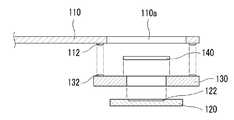
110: 인터페이스 인쇄회로기판110a: 실장 홀110: interface printed
112,132: 접속패드120: 이미지센서112,132: Connection pad 120: Image sensor
122: 픽셀영역130: 하드 인쇄회로기판122: pixel area 130: hard printed circuit board
130a: 노출홀140: IR필터130a: exposure hole 140: IR filter
본 발명은 카메라 모듈에 관한 것으로, 더욱 상세하게는 이미지 센서가 SMT방식으로 기판에 부착된 카메라 모듈용 디바이스에 관한 것이다.The present invention relates to a camera module, and more particularly, to a device for a camera module in which the image sensor is attached to the substrate by the SMT method.
최근들어, 셀룰러폰이나 PDA, PMP 등과 같이 휴대용 전자제품들이 널리 보급되고 그 서비스 내용도 점차 멀티미디어화되면서 이미지를 간편하게 촬상할 수 있는 카메라 모듈의 수요가 급격히 증가하고 있다.In recent years, as portable electronic products such as cellular phones, PDAs, and PMPs are widely used and their contents are increasingly multimedia, the demand for camera modules that can easily capture images is rapidly increasing.
종래의 카메라 모듈은 도 1에 도시된 바와 같이, 플랙시블 PCB(FPCB;10)상에 본딩기술을 적용하여 이미지 센서(16)를 실장한 후, 이미지 센서(16)를 감싸도록 하우징(20)과 결합하고, 하우징의 돌출부(22)에 렌즈홀더(30)를 부착한 구조로 이루어져 있다. 이때 플랙시블 PCB(10)는 카메라 모듈이 탑재되는 전자제품(예컨대, 휴대폰)의 메인보드와 인터페이스하기 위하여 측면으로 길게 확장됨과 아울러 확장면상에 인터페이스를 위한 커넥터(12)가 부착되어 있다.As shown in FIG. 1, the conventional camera module mounts the
통상, 이러한 카메라 모듈은 카메라 모듈 생산 전문업체에서 제조된 후 휴대폰 등과 같이 카메라 모듈을 사용하는 전자제품의 제조업체로 납품되어 전자제품의 메인보드에 실장되게 된다.Typically, such a camera module is manufactured by a camera module production company and then delivered to a manufacturer of an electronic product using a camera module such as a mobile phone and mounted on a main board of the electronic product.
그런데 종래의 카메라 모듈은, 도 1과 같이 하우징과 결합된 완제품 상태로 거래되므로 전자제품 생산자가 전자제품의 모델을 변경할 경우에 카메라 모듈 생산 전문업체에 전자제품의 새로운 모델에 맞는 카메라 모듈의 설계를 요구해야 하였고, 이에 따라 카메라 모듈 생산 전문업체는 새로 설계 및 제조하여 납품해야 하므로 카메라 모듈의 제조 및 전자제품의 모델변경에 시간이 많이 소요되는 문제점이 있었다.However, since the conventional camera module is traded in the state of the finished product combined with the housing as shown in FIG. 1, when the electronic product producer changes the model of the electronic product, a camera module production specialist may design a camera module for a new model of the electronic product. As a result, a professional manufacturer of camera module has to design, manufacture and deliver a new product. Therefore, there is a problem in that it takes a long time to manufacture a camera module and change a model of an electronic product.
본 발명은 상기와 같은 문제점을 해결하기 위하여 제안된 것으로, 본 발명의 목적은 카메라 모듈을 사용하는 전자제품의 생산자가 전자제품의 모델에 따라 카메라 모듈을 자유롭게 설계하여 제조할 수 있도록 된 반제품 형태의 카메라 모듈용 디바이스를 제공하는 것이다.The present invention has been proposed to solve the above problems, and an object of the present invention is to provide a semi-finished product that allows a producer of an electronic product using a camera module to freely design and manufacture a camera module according to a model of the electronic product. It is to provide a device for a camera module.
상기와 같은 목적을 달성하기 위한 본 발명의 카메라 모듈용 디바이스는, 카메라 하우징을 탑재할 수 있도록 된 카메라 모듈용 디바이스에 있어서, 카메라 모듈이 탑재될 메인보드와 인터페이스를 담당하고 실장 홀이 형성되어 있으며, 상기 실장 홀 주위에 SMT용 접속 패드가 부착된 인터페이스 인쇄회로기판; 중앙부분에 사각 형상의 노출 홀이 형성되어 있고, 상기 노출 홀의 주위에 상기 인터페이스 인쇄회로기판과 접속을 위한 SMT용 접속패드가 형성된 하드 인쇄회로기판; 상기 하드 인쇄회로기판의 노출홀 일면에 본딩된 이미지센서; 및 상기 하드 인쇄회로기판의 노출홀 타면에 부착된 투광성 보호커버를 포함하는 것을 특징으로 한다.The camera module device of the present invention for achieving the above object, in the camera module device that can be mounted on the camera housing, the interface with the main board on which the camera module is to be mounted and the mounting hole is formed An interface printed circuit board having a connection pad for SMT attached around the mounting hole; A hard printed circuit board having a rectangular exposed hole formed in a center portion thereof, and a connection pad for SMT for connection with the interface printed circuit board formed around the exposed hole; An image sensor bonded to one surface of an exposure hole of the hard printed circuit board; And a transparent protective cover attached to the other surface of the exposed hole of the hard printed circuit board.
상기 인터페이스 인쇄회로기판은 상면에 접속패드가 형성되어 있고, 상기 하드 인쇄회로기판은 하면에 인쇄회로기판이 형성되어 상기 하드 인쇄회로기판과 인터페이스 인쇄회로기판은 상기 이미지센서가 부착된 면에서 서로 접속되거나 상기 인터페이스 인쇄회로기판은 하면에 접속패드가 형성되어 있고, 상기 하드 인쇄회로기판은 상면에 인쇄회로기판이 형성되어 상기 하드 인쇄회로기판과 인터페이스 인쇄회로기판은 상기 이미지센서가 부착된 반대면에서 서로 접속될 수 있다.The interface printed circuit board has a connection pad formed on an upper surface thereof, and the hard printed circuit board has a printed circuit board formed on a lower surface thereof so that the hard printed circuit board and the interface printed circuit board are connected to each other at the surface where the image sensor is attached. Or the interface printed circuit board has a connection pad formed on a bottom surface thereof, and the hard printed circuit board has a printed circuit board formed on an upper surface thereof so that the hard printed circuit board and the interface printed circuit board are provided on the opposite side to which the image sensor is attached. Can be connected to each other.
그리고 상기 투광성 보호커버는 IR 필터 또는 커버 글래스 중 어느 하나이다.The translucent protective cover is any one of an IR filter or a cover glass.
이하, 첨부된 도면을 참조하여 본 발명의 바람직한 실시예를 자세히 설명하기로 한다.Hereinafter, exemplary embodiments of the present invention will be described in detail with reference to the accompanying drawings.
먼저, 본 발명에 따른 카메라 모듈용 디바이스는 SMT용 접속단자의 위치에 따라 SMT용 접속단자가 이미지 센서 측에 형성된 제1 실시예와 SMT용 접속단자가 이미지 센서의 반대 측에 형성된 제2 실시예로 구분하여 설명하기로 한다. 이해의 편의를 위해 본 발명의 실시예에서는 이미지 센서로 빛이 들어오는 방향을 상측으로 정의하여 설명한다.First, the camera module device according to the present invention has a first embodiment in which the SMT connection terminal is formed on the image sensor side and a second embodiment in which the SMT connection terminal is formed on the opposite side of the image sensor according to the position of the SMT connection terminal. The description will be divided into. For convenience of understanding, the embodiment of the present invention defines the direction in which light is input to the image sensor to the upper side.
[제1 실시예][First Embodiment]
본 발명에 따른 제1 실시예의 카메라 모듈용 디바이스는 도 2 내지 도 4에 도시된 바와 같이, 카메라 모듈이 탑재될 메인보드(미도시)와 인터페이스를 담당하고 카메라 모듈이 실장될 위치에 실장 홀(110a)이 형성되어 있으며 상기 실장 홀 (110a) 주위의 상면에 SMT용 접속 패드(112)가 부착된 인터페이스 인쇄회로기판(110)과, 중앙부분에 사각 형상의 노출 홀(130a)이 형성되어 있고 상기 노출 홀(130a)의 주위 하면에 상기 인터페이스 인쇄회로기판(110)과 접속을 위한 SMT용 접속패드(132)가 형성된 하드 인쇄회로기판(130)과, 상기 하드 인쇄회로기판(130)의 노출 홀(130a)의 하면에 본딩된 이미지센서(120)와, 상기 하드 인쇄회로기판(130)의 노출 홀(130a) 상면에 부착된 투광성 보호커버(140)로 구성된다. 투광성 보호커버(140)는 바람직하게는 IR 필터나 투명 고내열성 글래스 등으로 구현되어 빛을 통과시키거나 필터링함과 아울러 이미지센서(120)를 보호할 수 있도록 되어 있다.The device for a camera module of the first embodiment according to the present invention is responsible for the interface with the main board (not shown) on which the camera module is to be mounted, as shown in FIGS. An interface printed
이와 같은 발명에 따른 제1 실시예의 카메라 모듈용 디바이스는 보호커버(140)에 의해 이미지센서(120)를 보호할 수 있으므로 반제품 상태로 거래할 수 있고, 이에 따라 카메라 모듈을 사용하는 전자제품 생산자나 카메라 모듈 생산 전문업체에서는 하우징과 인터페이스부분만을 원하는 형태로 설계하여 신속하게 카메라 모듈을 완성할 수 있다.The device for a camera module of the first embodiment according to the present invention can protect the
도 2 내지 도 4를 참조하면, 인터페이스 인쇄회로기판(110)은 예컨대, 플랙시블 PCB(FPCB)의 일면에 하드PCB의 접속패드와 접속하기 위한 접속패드(112)와, 메인보드측에 접속되기 위한 커넥터(미도시)가 형성되어 있고, 접속패드(112)와 커넥터는 미도시된 도전패턴으로 연결되어 있다. 이러한 인터페이스 인쇄회로기판(110)의 형상은 메인보드의 요구규격에 따라 다양하게 구현될 수 있고, 커넥터가 부착된 FPCB 대신에 ZIF타입의 FPCB를 사용할 수도 있다.2 to 4, the interface printed
이미지 센서(120)는 n x m 픽셀 영역(122)을 포함하는 반도체칩으로서 미도시된 카메라 하우징의 렌즈로부터 빛을 수광하여 전기적인 신호로 변환한다. 이미지 센서(120)를 하드 인쇄회로기판(130)에 본딩함에 있어서는 플립칩 본딩기술 등이 적용될 수 있고, 도면에는 자세히 도시하지 않았으나 이미지 센서(120) 외에 다른 회로부품들이 부가적으로 실장될 수도 있다. 특히, 본 발명의 제1 실시예에 따른 카메라 모듈용 디바이스는 하드 인쇄회로기판(130)의 하면에 이미지 센서(120)가 부착되어 렌즈 홀더에 실장된 렌즈로부터 이미지 센서(120)까지의 거리(높이)를 확보하기 용이하도록 되어 있고, 이에 따라 카메라 모듈 전체의 높이를 낮출 수 있다.The
하드 인쇄회로기판(130)은 중앙에 이미지센서(120)의 픽셀영역(122)을 노출시키기 위한 노출 홀(130a)이 형성되어 있고, 노출 홀(130a)의 하면에는 인터페이스 인쇄회로기판(110)과 접속하기 위한 SMT용 접속패드(132)가 형성되어 있다.The hard printed
[제2 실시예]Second Embodiment
본 발명에 따른 제2 실시예의 카메라 모듈용 디바이스는 도 5 내지 도 7에 도시된 바와 같이, 카메라 모듈이 탑재될 메인보드(미도시)와 인터페이스를 담당하 고 카메라 모듈이 실장될 위치에 실장 홀(110a)이 형성되어 있으며 상기 실장 홀 (110a) 주위의 하면에 SMT용 접속 패드(112)가 부착된 인터페이스 인쇄회로기판(110)과, 중앙부분에 사각 형상의 노출 홀(130a)이 형성되어 있고 상기 노출 홀(130a)의 주위 상면에 상기 인터페이스 인쇄회로기판(110)과 접속을 위한 SMT용 접속패드(132)가 형성된 하드 인쇄회로기판(130)과, 상기 하드 인쇄회로기판(130)의 노출 홀(130a)의 하면에 본딩된 이미지센서(120)와, 상기 하드 인쇄회로기판(130)의 노출 홀(130a) 상면에 부착된 투광성 보호커버(140)로 구성된다. 투광성 보호커버(140)는 바람직하게는 IR 필터나 고내열성 투명 글래스 등으로 구현되어 빛을 통과시키거나 필터링함과 아울러 이미지센서(120)를 보호할 수 있도록 되어 있다.The device for a camera module of the second embodiment according to the present invention is responsible for the interface with the main board (not shown) on which the camera module is to be mounted, as shown in FIGS. 5 to 7, and a mounting hole at a position where the camera module is to be mounted. An interface printed
도 5 내지 도 7을 참조하면, 인터페이스 인쇄회로기판(110)은 예컨대, 플랙시블 PCB(FPCB)의 일면에 하드PCB의 접속패드와 접속하기 위한 접속패드(112)와, 메인보드측에 접속되기 위한 커넥터(미도시)가 형성되어 있고, 접속패드(112)와 커넥터는 미도시된 도전패턴으로 연결되어 있다. 이러한 인터페이스 인쇄회로기판(110)의 형상은 메인보드의 요구규격에 따라 다양하게 구현될 수 있고, 커넥터가 부착된 FPCB 대신에 ZIF타입의 FPCB를 사용할 수도 있다.5 to 7, the interface printed
이미지 센서(120)는 n x m 픽셀 영역(122)을 포함하는 반도체칩으로서 미도시된 카메라 하우징의 렌즈로부터 빛을 수광하여 전기적인 신호로 변환한다. 이미지 센서(120)를 하드 인쇄회로기판(130)에 본딩함에 있어서는 플립칩 본딩기술 등이 적용될 수 있고, 도면에는 자세히 도시하지 않았으나 이미지 센서(120) 외에 다 른 회로부품들이 부가적으로 실장될 수도 있다. 특히, 본 발명의 제1 실시예에 따른 카메라 모듈용 디바이스는 하드 인쇄회로기판(130)의 하면에 이미지 센서(120)가 부착되어 렌즈 홀더에 실장된 렌즈로부터 이미지 센서(120)까지의 거리(높이)를 확보하기 용이하도록 되어 있고, 이에 따라 카메라 모듈 전체의 높이를 낮출 수 있다.The
하드 인쇄회로기판(130)은 중앙에 이미지센서(120)의 픽셀영역(122)을 노출시키기 위한 노출 홀(130a)이 형성되어 있고, 노출 홀(130a)의 상면에는 인터페이스 인쇄회로기판(110)과 접속하기 위한 SMT용 접속패드(132)가 형성되어 있다.The hard printed
이러한 제2 실시예는 제1 실시예와 대비해 인터페이스 인쇄회로기판(110)이 이미지센서(120)의 반대편에 위치한다는 차이점이 있고, 이로 인해 제1 실시예와 달리 사이드 실링(Side sealing)을 위해 공간확보가 불필요하여 보다 사이즈를 축소할 수 있다.This second embodiment differs from the first embodiment in that the interface printed
이상에서 설명한 바와 같이, 본 발명에 따른 카메라 모듈용 디바이스는 인터페이스보드에 실장을 위한 홀이 형성됨과 아울러 하드 인쇄회로기판의 두께를 낮게하여 디바이스의 두께를 줄일 수 있고, 하드 인쇄회로기판의 하면에 이미지 센서가 부착되어 렌즈 홀더에 실장된 렌즈로부터 이미지 센서까지의 거리(높이)를 확보하기 용이하도록 되어 있고, 이에 따라 카메라 모듈 전체의 높이를 낮출 수 있다.As described above, the device for a camera module according to the present invention can reduce the thickness of the device by lowering the thickness of the hard printed circuit board and the hole for mounting on the interface board, the lower surface of the hard printed circuit board An image sensor is attached to facilitate a distance (height) from the lens mounted on the lens holder to the image sensor, thereby lowering the height of the entire camera module.
상기에서는 본 발명의 바람직한 실시예를 참조하여 설명하였지만, 해당 기술 분야의 숙련된 당업자는 하기의 특허 청구 범위에 기재된 본 발명의 사상 및 영역으로부터 벗어나지 않는 범위 내에서 본 발명을 다양하게 수정 및 변경시킬 수 있음을 이해할 수 있을 것이다.While the foregoing has been described with reference to preferred embodiments of the present invention, those skilled in the art will be able to variously modify and change the present invention without departing from the spirit and scope of the invention as set forth in the claims below. It will be appreciated.
Claims (4)
Translated fromKoreanPriority Applications (1)
| Application Number | Priority Date | Filing Date | Title |
|---|---|---|---|
| KR1020060085181AKR20060104962A (en) | 2006-09-05 | 2006-09-05 | Device for camera module |
Applications Claiming Priority (1)
| Application Number | Priority Date | Filing Date | Title |
|---|---|---|---|
| KR1020060085181AKR20060104962A (en) | 2006-09-05 | 2006-09-05 | Device for camera module |
Publications (1)
| Publication Number | Publication Date |
|---|---|
| KR20060104962Atrue KR20060104962A (en) | 2006-10-09 |
Family
ID=37634888
Family Applications (1)
| Application Number | Title | Priority Date | Filing Date |
|---|---|---|---|
| KR1020060085181AAbandonedKR20060104962A (en) | 2006-09-05 | 2006-09-05 | Device for camera module |
Country Status (1)
| Country | Link |
|---|---|
| KR (1) | KR20060104962A (en) |
Cited By (4)
| Publication number | Priority date | Publication date | Assignee | Title |
|---|---|---|---|---|
| KR100924673B1 (en)* | 2008-04-15 | 2009-11-03 | (주)미코엠에스티 | Liquid lens camera module |
| KR100928011B1 (en)* | 2007-12-20 | 2009-11-24 | 삼성전기주식회사 | Image sensor module and manufacturing method thereof, and a camera module including the same |
| KR101294534B1 (en)* | 2006-12-07 | 2013-08-07 | 엘지이노텍 주식회사 | Camera module |
| WO2016199965A1 (en)* | 2015-06-12 | 2016-12-15 | 재단법인 다차원 스마트 아이티 융합시스템 연구단 | Optical system comprising aperture board having non-circle shape and multi-aperture camera comprising same |
- 2006
- 2006-09-05KRKR1020060085181Apatent/KR20060104962A/ennot_activeAbandoned
Cited By (4)
| Publication number | Priority date | Publication date | Assignee | Title |
|---|---|---|---|---|
| KR101294534B1 (en)* | 2006-12-07 | 2013-08-07 | 엘지이노텍 주식회사 | Camera module |
| KR100928011B1 (en)* | 2007-12-20 | 2009-11-24 | 삼성전기주식회사 | Image sensor module and manufacturing method thereof, and a camera module including the same |
| KR100924673B1 (en)* | 2008-04-15 | 2009-11-03 | (주)미코엠에스티 | Liquid lens camera module |
| WO2016199965A1 (en)* | 2015-06-12 | 2016-12-15 | 재단법인 다차원 스마트 아이티 융합시스템 연구단 | Optical system comprising aperture board having non-circle shape and multi-aperture camera comprising same |
Similar Documents
| Publication | Publication Date | Title |
|---|---|---|
| CN108196388B (en) | Display device and manufacturing method thereof | |
| US8248523B2 (en) | Camera module with fold over flexible circuit and cavity substrate | |
| CN101611468B (en) | Folded package camera module and method of manufacture | |
| US20160150133A1 (en) | Electronic device module having an imaging unit | |
| KR101070058B1 (en) | Camera Module Package | |
| US20070200053A1 (en) | Image pickup apparatus, camera module, electronic device, and fabrication method for image pickup apparatus | |
| CN108322632A (en) | Camera module, electronic device and camera module manufacturing method | |
| JP2007274624A (en) | Camera module | |
| US11303788B2 (en) | Electronic device and camera module thereof | |
| US10388685B2 (en) | Portable electronic device and image-capturing module thereof, and image-sensing assembly thereof | |
| US10313573B2 (en) | Portable electronic device and image-capturing module thereof, and carrier assembly thereof | |
| KR20150030904A (en) | Camera module | |
| CN108174080A (en) | A camera module and mobile terminal | |
| KR20060104962A (en) | Device for camera module | |
| US20180241859A1 (en) | Printed circuit board and mobile terminal mounted the same | |
| KR102185063B1 (en) | Sensing package and manufacturing method for the same | |
| US20070173084A1 (en) | Board-to-board connecting structure | |
| JP6743219B2 (en) | Imaging module and portable electronic device | |
| KR100947967B1 (en) | Camera module and its manufacturing method | |
| KR20100041383A (en) | Camera module | |
| KR101026830B1 (en) | Camera module | |
| KR100772664B1 (en) | Device for camera module and camera module using same | |
| KR20110099528A (en) | Camera module | |
| KR20100002536U (en) | Camera module | |
| KR102477249B1 (en) | Camera module |
Legal Events
| Date | Code | Title | Description |
|---|---|---|---|
| A201 | Request for examination | ||
| PA0109 | Patent application | Patent event code:PA01091R01D Comment text:Patent Application Patent event date:20060905 | |
| PA0201 | Request for examination | ||
| G15R | Request for early publication | ||
| PG1501 | Laying open of application | Comment text:Request for Early Opening Patent event code:PG15011R01I Patent event date:20060913 | |
| E902 | Notification of reason for refusal | ||
| PE0902 | Notice of grounds for rejection | Comment text:Notification of reason for refusal Patent event date:20070928 Patent event code:PE09021S01D | |
| E701 | Decision to grant or registration of patent right | ||
| PE0701 | Decision of registration | Patent event code:PE07011S01D Comment text:Decision to Grant Registration Patent event date:20080325 | |
| NORF | Unpaid initial registration fee | ||
| PC1904 | Unpaid initial registration fee |