KR20060079958A - Silicon Thin Film Transistor - Google Patents
Silicon Thin Film TransistorDownload PDFInfo
- Publication number
- KR20060079958A KR20060079958AKR1020050000381AKR20050000381AKR20060079958AKR 20060079958 AKR20060079958 AKR 20060079958AKR 1020050000381 AKR1020050000381 AKR 1020050000381AKR 20050000381 AKR20050000381 AKR 20050000381AKR 20060079958 AKR20060079958 AKR 20060079958A
- Authority
- KR
- South Korea
- Prior art keywords
- thin film
- insulating layer
- gate insulating
- silicon
- gate
- Prior art date
- Legal status (The legal status is an assumption and is not a legal conclusion. Google has not performed a legal analysis and makes no representation as to the accuracy of the status listed.)
- Withdrawn
Links
Images


Classifications
- H—ELECTRICITY
- H10—SEMICONDUCTOR DEVICES; ELECTRIC SOLID-STATE DEVICES NOT OTHERWISE PROVIDED FOR
- H10D—INORGANIC ELECTRIC SEMICONDUCTOR DEVICES
- H10D30/00—Field-effect transistors [FET]
- H10D30/60—Insulated-gate field-effect transistors [IGFET]
- H10D30/67—Thin-film transistors [TFT]
- H10D30/6729—Thin-film transistors [TFT] characterised by the electrodes
- H10D30/6737—Thin-film transistors [TFT] characterised by the electrodes characterised by the electrode materials
- H10D30/6739—Conductor-insulator-semiconductor electrodes
- H—ELECTRICITY
- H10—SEMICONDUCTOR DEVICES; ELECTRIC SOLID-STATE DEVICES NOT OTHERWISE PROVIDED FOR
- H10D—INORGANIC ELECTRIC SEMICONDUCTOR DEVICES
- H10D30/00—Field-effect transistors [FET]
- H10D30/01—Manufacture or treatment
- H10D30/021—Manufacture or treatment of FETs having insulated gates [IGFET]
- H10D30/031—Manufacture or treatment of FETs having insulated gates [IGFET] of thin-film transistors [TFT]
- H10D30/0312—Manufacture or treatment of FETs having insulated gates [IGFET] of thin-film transistors [TFT] characterised by the gate electrodes
- H10D30/0314—Manufacture or treatment of FETs having insulated gates [IGFET] of thin-film transistors [TFT] characterised by the gate electrodes of lateral top-gate TFTs comprising only a single gate
- H—ELECTRICITY
- H10—SEMICONDUCTOR DEVICES; ELECTRIC SOLID-STATE DEVICES NOT OTHERWISE PROVIDED FOR
- H10D—INORGANIC ELECTRIC SEMICONDUCTOR DEVICES
- H10D30/00—Field-effect transistors [FET]
- H10D30/01—Manufacture or treatment
- H10D30/021—Manufacture or treatment of FETs having insulated gates [IGFET]
- H10D30/031—Manufacture or treatment of FETs having insulated gates [IGFET] of thin-film transistors [TFT]
- H10D30/0321—Manufacture or treatment of FETs having insulated gates [IGFET] of thin-film transistors [TFT] comprising silicon, e.g. amorphous silicon or polysilicon
Landscapes
- Thin Film Transistor (AREA)
Abstract
Translated fromKoreanDescription
Translated fromKorean도 1은 본 발명에 따른 박막트랜지스터(TFT)의 개략적 단면도이다.1 is a schematic cross-sectional view of a thin film transistor (TFT) according to the present invention.
도 2a 내지 도 2l는 본 발명에 따른 TFT의 제조방법의 개략적 공정 흐름도이다.2A to 2L are schematic process flowcharts of a method of manufacturing a TFT according to the present invention.
도 3 은 본 발명에 따른 샘플과 이에 대비되는 비교예의 샘플의 게이트절연층의 캐패시턴스 특성을 비교해 보이는 그래프이다.3 is a graph comparing capacitance characteristics of a gate insulating layer of a sample according to the present invention and a sample of a comparative example.
도 4는 본 발명에 따른 샘플과 이에 대비되는 비교예의 샘플의 게이트절연층의 전류누설특성을 비교해 보이는 그래프이다.4 is a graph comparing current leakage characteristics of a gate insulating layer of a sample according to the present invention and a sample of a comparative example.
본 발명은 누설전류가 감소된 실리콘 박막트랜지스터(silicon thin film transistor)에 관한 것이다.The present invention relates to a silicon thin film transistor with reduced leakage current.
다결정 실리콘(poly crystalline Si, poly-Si)은 비정질 실리콘(amorphous Si, a-Si)에 비해 높은 이동도(mobility)를 가지기 때문에 평판 디스플레이 소자 뿐 아니라 태양전지 등 다양한 전자 소자등에 응용된다.Poly crystalline Si (poly-Si) has a higher mobility than amorphous Si (a-Si), so it is applied to various electronic devices such as solar cells as well as flat panel display devices.
일반적으로 양질의 다결정 실리콘 결정을 얻기 위해서는 열에 강한 재료 예 를 들어 유리 등이 이용된다. 유리와 같이 열에 강한 재료에 형성되는 다결정 실리콘의 제조에는 CVD 또는 PECVD 와 같은 고온하에서의 a-Si 증착법이 이용되며 이러한 종래 방법에 의해 얻을 수 있는 결정입자의 최대 크기는 약 3000 ~ 4000Å 정도이며 그 이상의 크기는 얻기 매우 어려운 것으로 알려져 있다. 따라서, 보다 큰 입경을 가지는 다결정 실리콘의 제조기술의 개발은 하나의 과제로 남아 있다.In general, in order to obtain high quality polycrystalline silicon crystals, a heat resistant material such as glass is used. In the production of polycrystalline silicon formed on a heat resistant material such as glass, a-Si deposition method under high temperature such as CVD or PECVD is used, and the maximum crystal grain size that can be obtained by such a conventional method is about 3000 to 4000Å and more. Size is known to be very difficult to obtain. Therefore, development of a manufacturing technology of polycrystalline silicon having a larger particle size remains a problem.
한편, 최근에는 플라스틱 기판에 다결정 실리콘 전자소자를 형성하는 방법이 연구되고 있다. 플라스틱의 열변형을 방지하기 위하여 다결정 실리콘 전자소자를 형성하기 위한 스퍼터링과 같은 소위 저온 공정(low temperature process)의 도입이 불가피하다. 이러한 저온 공정은 기판에 대한 열충격을 방지하기 위해서도 필요하고 나아가서는 소자 제조시 고온 공정에서 발생되는 공정 결함을 억제하기 위해서도 필요하다. 플라스틱 기판은 열에 약한 단점 외에 가볍고 유연하면서도 튼튼한 장점을 가지기 때문에 최근에 평판 디스플레이 소자의 기판으로서 연구되고 있다.On the other hand, in recent years, a method of forming a polycrystalline silicon electronic device on a plastic substrate has been studied. In order to prevent thermal deformation of plastics, the introduction of so-called low temperature processes such as sputtering for forming polycrystalline silicon electronic devices is inevitable. This low temperature process is also necessary to prevent thermal shock to the substrate, and furthermore, to suppress process defects generated in the high temperature process during device manufacturing. Plastic substrates have recently been studied as substrates for flat panel display devices because they have a light, flexible, and durable advantage in addition to the disadvantages of heat.
캐리 등(Carry et. al, 미국특허 5,817,550호)은 실리콘 채널을 플라스틱 기판에 형성하는 공정에서 플라스틱의 손상을 방지할 수 있는 방법을 제시한다.Carry et. Al (US Pat. No. 5,817,550) proposes a method for preventing damage to plastics in the process of forming a silicon channel on a plastic substrate.
다결정 실리콘 TFT의 게이트절연층으로 사용되는 SiO2는 상호컨덕턴스(gm)이 3.8 정도로 제한된다. 이러한 게이트 절연층은 전류누설이 크고 항복 전압이 낮기 때문에 저온성장 다결정실리콘(LTPS) TFT에는 적용되기 어렵다.SiO2 used as the gate insulating layer of the polycrystalline silicon TFT is limited to a mutual conductance (gm) of about 3.8. Such a gate insulating layer is difficult to be applied to low temperature growth polysilicon (LTPS) TFTs because of large current leakage and low breakdown voltage.
TFT를 구성하는 핵심 요소인 게이트 절연막은 TFT의 동작 특성에 크게 그리 고 직접적으로 영향을 미치는 것으로 알려져 있다. 따라서 현재 차세대 TFT의 게이트 절연막에 적합한 물질 및 공정을 개발하기 위한 광범위한 연구가 진행되고 있다. 특히 다결정 또는 비정질 Si 기판과 게이트 절연막 사이의 계면에서 발생하는 결함, 즉 인터페이스 트랩(interface trap)을 최소화시켜 TFT의 트랜스컨덕턴스(transconductance)를 향상시킬 수 있고, 절연파괴 전압(breakdown voltage)을 높일 수 있는 새로운 물질과 이들을 안정적으로 성장시킬 수 있는 공정개발이 요구된다. 그리고 현재 게이트 절연막으로 활용되는 SiOx 산화막 보다 큰 유전율을 가짐으로써 전류 구동능력을 향상시키고 게이트 절연막의 내부에 존재하는 결함을 최소화하여 이력(hysteresis) 특성을 최소화할 수 있는 기술 개발이 절실하다. HfO2는 이러한 요구 조건을 만족시키는 물질 중에 하나이다. 하지만 이러한 HfO2는 고온에서 결정질상을 갖는 특징으로 누설 전류가 크다는 것이 하나의 문제로 제기되고 있다.The gate insulating film, which is a key component of the TFT, is known to greatly and directly affect the operation characteristics of the TFT. Therefore, extensive research is currently underway to develop materials and processes suitable for the gate insulating film of the next-generation TFT. In particular, defects occurring at the interface between the polycrystalline or amorphous Si substrate and the gate insulating layer, i.e., interface traps can be minimized, thereby improving the transconductance of the TFTs and increasing the breakdown voltage. New materials and processes that can grow them stably are required. In addition, since the dielectric constant is larger than that of the SiOx oxide film currently used as a gate insulating film, a technology for improving current driving capability and minimizing defects present in the gate insulating film is needed to minimize hysteresis characteristics. HfO2 is one of the materials that meets these requirements. However, such a HfO2 has a crystalline phase at a high temperature, a large leakage current has been raised as a problem.
본 발명은 HfO2를 사용할 때 누설 전류를 줄이기 위해서 초박막 SiO2 박막을 HfO2 박막 밑에 사용함으로써 SiO2 박막이 갖는 좋은 절연 특성과 함께 HfO2 박막의 큰 유전 특성을 이용하는 TFT에 관련된다.The present invention relates to a TFT using the large dielectric properties of HfO2 thin films with a good insulating property having a SiO2 thin film by using an ultra-thin SiO2 thin film under the HfO2 thin film to reduce the leakage current when using the HfO2.
본 발명은 낮은 누설전류의 계면특성을 가지는 다결정 실리콘 TFT를 제공함에 그 목적이 있다.It is an object of the present invention to provide a polycrystalline silicon TFT having an interfacial property of low leakage current.
본 발명에 따른 다결정 실리콘 TFT는:The polycrystalline silicon TFT according to the present invention is:
기판과;A substrate;
기판에 형성되는 것으로 그 양측에 소스와 드레인이 마련되는 실리콘 채널과;A silicon channel formed on the substrate and having a source and a drain disposed on both sides thereof;
상기 실리콘 채널 위에 형성되는 게이트 절연층과;A gate insulating layer formed on the silicon channel;
상기 게이트 절연층 위에 마련되는 게이트를; 구비하고,A gate provided on the gate insulating layer; Equipped,
상기 게이트 절연층은 HfOx박막을 포함하는 것을 특징으로 한다.The gate insulating layer is HfOx It characterized in that it comprises a thin film.
상기 본 발명의 바람직한 실시예에 따르면,According to a preferred embodiment of the present invention,
상기 게이트 절연층은 HfOx 박막 및 SiO2 박막을 구비한다.The gate insulating layer includes an HfOx thin film and a SiO2 thin film.
상기 HfOx 는 고유전물질로서 500℃ 이하의 저온 공정에서 형성된다.The HfOx is formed in a low temperature process of 500 ° C. or less as a high dielectric material.
상기 게이트 절연층은 100nm 이하의 두께를 가지며, 상기 기판은 실리콘, 유리 또는 플라스틱 기판이다.The gate insulating layer has a thickness of 100 nm or less, and the substrate is a silicon, glass or plastic substrate.
이하 첨부된 도면을 참조하면서 본 발명에 따른 다결정 실리콘 TFT의 바람직한 실시예를 상세히 설명한다.Hereinafter, preferred embodiments of the polycrystalline silicon TFT according to the present invention will be described in detail with reference to the accompanying drawings.
도 1은 본 발명에 따른 다결정 실리콘 TFT의 개략적 단면도이다.1 is a schematic cross-sectional view of a polycrystalline silicon TFT according to the present invention.
도 1을 참조하면, 실리콘, 유리(glass) 또는 플라스틱 기판(10) 위에 절연층(11)이 마련되고 이 위에 실리콘 채널층(12)이 마련된다. 실리콘 채널층(12)의 양측에는 도핑에 의한 소스(12a) 및 드레인(12b) 영역이 마련되어 있다. 상기 채널층(12)의 위에는 본 발명을 특징지우는 게이트 절연층(13)이 마련되고, 이 위의 중앙 에 게이트(14)가 형성되어 있다. 게이트(14)의 위에는 ILD(interlayer dielectric, 15)이 형성되어 있다. ILD에서 역시 상기 소오스 전극(Source Electrode)과 드레인 전극(Drain Electrode) 대응하는 부분에 관통공이 형성되어 있다. 소오스 전극(16)은 다결정 실리콘의 소오스에 연결되어 있고, 드레인 전극(17)은 다결정 실리콘의 드레인에 연결되어 있다.Referring to FIG. 1, an
위에서 본 발명을 특징지우는 게이트 절연층(13)은 하부의 SiO2층(13a) 과 이 위의 HfOx, 바람직하게는 HfO2층(13b)을 구비한다.
The
이하 첨부된 도면을 참조하면서 본 발명에 따른 TFT의 제조방법의 일례를 설명하다.Hereinafter, an example of a method of manufacturing a TFT according to the present invention will be described with reference to the accompanying drawings.
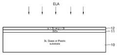
도 2a에 도시된 바와 같이, 다결정 실리콘 박막 형성을 위한 Si 웨이퍼, 유리또는 플라스틱 기판(10)을 준비한다. 기판(10) 위에는 전기적 절연 등을 위한 SiO2산화막(11)이 형성되어 있고, Si 웨이퍼의 경우에는 자연적인 산화막이 형성되어 있다.As shown in FIG. 2A, a Si wafer, glass, or
도 2b에 도시된 바와 같이, 상기 기판(10)의 절연층(11) 위에 비정질 실리콘 박막(a-Si, 12)을 형성한다. 비정질 실리콘 박막(12)은 스퍼터링 법등의 물리적 증착법(PVD, Physical Vapor Deposition)에 의해 형성한다. 이때에 저온 증착이 가능한 스퍼터링 법을 이용하는 스퍼터링 가스는 희가스 예를 들어 Ar을 이용한다. a-Si 의 두께는 50nm 가 되도록 조절한다. 스퍼터링 파워는 200W 그리고 가스압력은 5mTorr로 조절한다.As shown in FIG. 2B, an amorphous silicon thin film (a-Si) 12 is formed on the
도 2c에 도시된 바와 같이 비정질 실리콘 박막(12)을 퍼니스(furnace)나 ELA(Eximer Laser Annealling)에 의해 열처리하여 목적하는 다결정 실리콘(p-Si) 박막을 얻는다. 바람직하게는 열처리는 ELA를 이용한다.As shown in FIG. 2C, the amorphous silicon
TFT의 기판이 유리가 아닌 플라스틱 재료로 되었을 경우 SiO2 박막 열처리시 가해지는 열에 의해 기판이 변형되는 것은 방지되어야 하므로 SiO2 박막 열처리시의 온도는 적절히 절충되어야 한다.If the TFT substrate is a plastic material other than glass is the substrate is deformed by heat applied during the heat treatment must be prevented, because SiO2 thin film temperature in the SiO2 thin film is to be heat-treated properly trade-off.
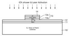
도 2d에 도시된 바와 같이, 상기 실리콘 박막(12) 위에 먼저 게이트 절연층(13)의 한 부분인 SiO2 박막(13a)을 형성한다.여기에서 SiO2 박막(13a)의 두께는 바람직하게 50nm 이하의 두께로 ICP-CVD, PE-CVD, 스퍼터링 법등에 의해 형성한다.As shown in Fig. 2D, an SiO2
도 2e에 도시된 바와 같이, CVD 법에 의해 상기 SiO2박막(13a) 위에 게이트 절연층(13)의 다른 한 부분인 HfOx, 바람직하게 HfO2박막(13b)을 스퍼터링법 등에 의해 형성한다. 이때에 HfO2박막(13b)의 두께는 50nm 이하로 조절한다. 공정은 500℃ 이하의 저온 하에서 실시한다.As shown in Fig. 2E, HfOx, preferably HfO2
도 2f에 도시된 바와 같이 상기 게이트 절연층(13) 위에 Al 등으로 게이트 (14)를 형성한다. 여기에서 위의 게이트 절연층(13)과 게이트(14)는 아직 형태상 주어진 기능을 수행할 수 형상을 가지면 후속되는 과정을 통해서 목적하는 최종 형 태로 패터닝된다.As shown in FIG. 2F, the
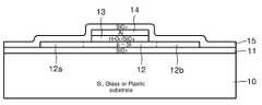
도 2g에 도시된 바와 같이, 제1마스크(M1)를 이용한 건식식각법에 의해 상기 게이트(14)와 게이트 절연층(13)을 식각한다. 상기 마스크(M)는 게이트의 형상에 대응하는 패턴을 가진다. 이러한 패턴에 의해 상기 게이트(21)가 패터닝되고 그 하부의 게이트 절연층(13)도 동일한 형상으로 패터닝된다. 이를 통해서 게이트(14)에 덮히지 않은 부분을 통해 실리콘 박막(12)이 노출된다.As illustrated in FIG. 2G, the
도 2h에 도시된 바와 같이, 이온 샤워를 통해 게이트(21)에 덮히지 않은 부분을 도핑하고 이에 이어 308nm XeCl 엑시머 레이저에 의해 활성화한다.As shown in FIG. 2H, the uncovered portion of the gate 21 is doped through an ion shower followed by activation by a 308 nm XeCl excimer laser.
도 2i에 도시된 바와 같이, 제2마스크(M2)를 이용한 건식식각법에 의해 상기 게이트에 덮이지 않은 실리콘 박막(12) 을 패터닝하여 소스(12a)와 드레인(12b)을 형성한다. 상기 게이트(21)의 하부에는 p-Si가 도핑되지 않은 상태로 잔류하며 이후 채널로서의 기능을 하게 된다.As illustrated in FIG. 2I, the silicon
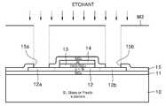
도 2j에 도시된 바와 같이 ICP-CVD, PE-CVD, 스퍼터링 등에 의해 상기 적층물 위에 ILD(interlayer dielectric)으로서 SiO2 제3절연층(15)을 약 3000Å의 두께로 형성한다.As shown in FIG. 2J, an SiO2 third insulating
도 2k에 도시된 바와 같이, 제3마스크(M3)를 이용하여 상기 SiO2 제3절연층(15)에 소스 콘택홀(15a) 및 게이트 콘택홀(15b)을 형성한다.As shown in FIG. 2K, a
도 2l에 도시된 바와 같이, 상기 소스 콘택홀(15a) 및 게이트 콘택홀(15b)위에 소스 전극(16) 및 드레인 전극(17)을 형성하여 목적하는 TFT를 얻는다.As shown in FIG. 2L, a
도 3은 본 발명에 따른 TFT의 특성을 검토하기 위하여 실시된 게이트 전압-게이트 캐패시턴스 특성 그래프이다. 이러한 테스트를 위해 Si 기판 위에 HfO2(500Å)/SiO2(100Å) 적층의 게이트 절연층(을 가지는 샘플1과 HfO2 (500Å) 단일층의 게이트 전연층을 갖는 샘플2를 제작하였다. HfO2 막 형성을 위한 조건은 아래와 같다.3 is a graph of gate voltage-gate capacitance characteristics implemented to examine the characteristics of a TFT according to the present invention. For this test were producedHfO 2 (500Å) / SiO 2 (100Å)
1) POWER :30W, 15 분1) POWER: 30W, 15 minutes
2) 가스 : Ar, 20sccm2) Gas: Ar, 20sccm
3) 공정압력 : 0.8mTorr3) Process Pressure: 0.8mTorr
4) Oxidation (furnace) : 500℃ / 4hr4) Oxidation (furnace): 500 ℃ / 4hr
5) 열처리(annealing) : RTA(rapid thermal annealing) : 500℃ /1min/N25) Annealing: RTA (rapid thermal annealing): 500 ℃ / 1min / N2
도 4는 상기 두 샘플의 전압-누설전류 특성을 보이는 그래프이다.4 is a graph showing the voltage-leakage current characteristics of the two samples.
측정에 의하면 본 발명에 따른 샘플1 및 비교예인 샘플2의 전기적 특성은 아래와 같다.According to the measurement, the electrical properties of
샘플 1 :Sample 1:
Vfb = 0.62V, Cox = 55pF, EOT=138Å, J = 3.58 * 10-7 (A/cm2) (@ -5V)Vfb = 0.62V, Cox = 55pF, EOT = 138Å, J = 3.58 * 10-7 (A / cm2 ) (@ -5V)
샘플 2 :Sample 2:
Vfb = 0.64V, Cox = 120pF, EOT= 68Å, J = 6.3 * 10-7 (A/cm2) (@ -5V)Vfb = 0.64V, Cox = 120pF, EOT = 68Å, J = 6.3 * 10-7 (A / cm2 ) (@ -5V)
도 3 및 도 4의 결과를 통해서 본 발명에 따라 HfOx/SiO2 적층구조의 게이 트 절연층은 감소된 전류누설특성 및 높은 용량(capacitance)를 가짐을 알수 있다.3 and 4, the gate insulation layer of the HfOx / SiO2 stacked structure according to the present invention has a reduced current leakage characteristic and a high capacitance.
상기와 같은 적층 구조의 게이트 절연층을 가지는 본 발명에 따른 TFT는 누설전류가 작은 계면특성을 가진다.The TFT according to the present invention having the gate insulating layer of the laminated structure as described above has an interfacial characteristic with a small leakage current.
이러한 본 발명의 TFT는 Si 기판 뿐 아니라 플라스틱이나 유리와 같은 열에 약한 재료에 형성될 수 있다.Such TFTs of the present invention can be formed not only on Si substrates but also on materials susceptible to heat such as plastic or glass.
이러한 본 발명의 TFT는 평판 표시소자, 예를 들어 AMLCD, AMOLED, 태양전지, 반도체 메모리 소자 등에 적용되기에 적합하다.Such a TFT of the present invention is suitable for application to flat panel display devices such as AMLCDs, AMOLEDs, solar cells, semiconductor memory devices, and the like.
이러한 본원 발명의 이해를 돕기 위하여 몇몇의 모범적인 실시예가 설명되고 첨부된 도면에 도시되었으나, 이러한 실시예들은 단지 넓은 발명을 예시하고 이를 제한하지 않는다는 점이 이해되어야 할 것이며, 그리고 본 발명은 도시되고 설명된 구조와 배열에 국한되지 않는다는 점이 이해되어야 할 것이며, 이는 다양한 다른 수정이 당 분야에서 통상의 지식을 가진 자에게 일어날 수 있기 때문이다.While some exemplary embodiments have been described and illustrated in the accompanying drawings in order to facilitate understanding of the present invention, it should be understood that these embodiments merely illustrate the broad invention and do not limit it, and the invention is illustrated and described. It is to be understood that the invention is not limited to structured arrangements and arrangements, as various other modifications may occur to those skilled in the art.
Claims (7)
Translated fromKoreanPriority Applications (2)
| Application Number | Priority Date | Filing Date | Title |
|---|---|---|---|
| KR1020050000381AKR20060079958A (en) | 2005-01-04 | 2005-01-04 | Silicon Thin Film Transistor |
| US11/322,235US20060145158A1 (en) | 2005-01-04 | 2006-01-03 | Poly-crystalline silicon thin film transistor |
Applications Claiming Priority (1)
| Application Number | Priority Date | Filing Date | Title |
|---|---|---|---|
| KR1020050000381AKR20060079958A (en) | 2005-01-04 | 2005-01-04 | Silicon Thin Film Transistor |
Publications (1)
| Publication Number | Publication Date |
|---|---|
| KR20060079958Atrue KR20060079958A (en) | 2006-07-07 |
Family
ID=36639358
Family Applications (1)
| Application Number | Title | Priority Date | Filing Date |
|---|---|---|---|
| KR1020050000381AWithdrawnKR20060079958A (en) | 2005-01-04 | 2005-01-04 | Silicon Thin Film Transistor |
Country Status (2)
| Country | Link |
|---|---|
| US (1) | US20060145158A1 (en) |
| KR (1) | KR20060079958A (en) |
Cited By (1)
| Publication number | Priority date | Publication date | Assignee | Title |
|---|---|---|---|---|
| KR20200101150A (en)* | 2019-02-19 | 2020-08-27 | 한양대학교 산학협력단 | High-permittivity transistor and manufacturing method thereof |
Families Citing this family (6)
| Publication number | Priority date | Publication date | Assignee | Title |
|---|---|---|---|---|
| KR101186292B1 (en)* | 2006-01-10 | 2012-09-27 | 삼성전자주식회사 | Transistor and fabrication method thereof and organic light emitting display adopting the transistor |
| US9196739B2 (en)* | 2010-04-02 | 2015-11-24 | Semiconductor Energy Laboratory Co., Ltd. | Semiconductor device including oxide semiconductor film and metal oxide film |
| JP5598145B2 (en)* | 2010-08-04 | 2014-10-01 | 富士通セミコンダクター株式会社 | Semiconductor device manufacturing method and semiconductor device |
| US9048160B2 (en)* | 2012-07-12 | 2015-06-02 | Carestream Health, Inc. | Radiographic imaging array fabrication process for metal oxide thin-film transistors with reduced mask count |
| CN103489920B (en)* | 2013-09-26 | 2016-08-17 | 京东方科技集团股份有限公司 | A kind of thin film transistor (TFT) and preparation method thereof, array base palte and display device |
| KR102216678B1 (en)* | 2014-07-14 | 2021-02-18 | 삼성디스플레이 주식회사 | Thin film transistor manufacturing method |
Family Cites Families (13)
| Publication number | Priority date | Publication date | Assignee | Title |
|---|---|---|---|---|
| US5817550A (en)* | 1996-03-05 | 1998-10-06 | Regents Of The University Of California | Method for formation of thin film transistors on plastic substrates |
| TW486581B (en)* | 1998-01-06 | 2002-05-11 | Seiko Epson Corp | Semiconductor device, substrate for electro-optical device, electro-optical device, electronic equipment, and projection display apparatus |
| US6653209B1 (en)* | 1999-09-30 | 2003-11-25 | Canon Kabushiki Kaisha | Method of producing silicon thin film, method of constructing SOI substrate and semiconductor device |
| US6380589B1 (en)* | 2001-01-30 | 2002-04-30 | Advanced Micro Devices, Inc. | Semiconductor-on-insulator (SOI) tunneling junction transistor SRAM cell |
| US6566213B2 (en)* | 2001-04-02 | 2003-05-20 | Advanced Micro Devices, Inc. | Method of fabricating multi-thickness silicide device formed by disposable spacers |
| US7358578B2 (en)* | 2001-05-22 | 2008-04-15 | Renesas Technology Corporation | Field effect transistor on a substrate with (111) orientation having zirconium oxide gate insulation and cobalt or nickel silicide wiring |
| JP2004348808A (en)* | 2003-05-20 | 2004-12-09 | Sharp Corp | Semiconductor storage device, portable electronic device, method for controlling erase operation, and method for controlling program operation |
| US7382421B2 (en)* | 2004-10-12 | 2008-06-03 | Hewlett-Packard Development Company, L.P. | Thin film transistor with a passivation layer |
| US20060211259A1 (en)* | 2005-03-21 | 2006-09-21 | Maes Jan W | Silicon oxide cap over high dielectric constant films |
| US20060231908A1 (en)* | 2005-04-13 | 2006-10-19 | Xerox Corporation | Multilayer gate dielectric |
| KR101186291B1 (en)* | 2005-05-24 | 2012-09-27 | 삼성전자주식회사 | Germanium on insulator structure and semiconductor device using the same |
| KR100653721B1 (en)* | 2005-06-30 | 2006-12-05 | 삼성전자주식회사 | Semiconductor device having nitrogen injection active region and manufacturing method |
| KR100655658B1 (en)* | 2005-07-26 | 2006-12-08 | 삼성전자주식회사 | Gate electrode structure and manufacturing method thereof, semiconductor transistor having same and manufacturing method thereof |
- 2005
- 2005-01-04KRKR1020050000381Apatent/KR20060079958A/ennot_activeWithdrawn
- 2006
- 2006-01-03USUS11/322,235patent/US20060145158A1/ennot_activeAbandoned
Cited By (1)
| Publication number | Priority date | Publication date | Assignee | Title |
|---|---|---|---|---|
| KR20200101150A (en)* | 2019-02-19 | 2020-08-27 | 한양대학교 산학협력단 | High-permittivity transistor and manufacturing method thereof |
Also Published As
| Publication number | Publication date |
|---|---|
| US20060145158A1 (en) | 2006-07-06 |
Similar Documents
| Publication | Publication Date | Title |
|---|---|---|
| US7563659B2 (en) | Method of fabricating poly-crystalline silicon thin film and method of fabricating transistor using the same | |
| US5275851A (en) | Low temperature crystallization and patterning of amorphous silicon films on electrically insulating substrates | |
| US7265393B2 (en) | Thin-film transistor with vertical channel region | |
| JP5015471B2 (en) | Thin film transistor and manufacturing method thereof | |
| KR20080104588A (en) | Method of manufacturing nano-type thin film transistor | |
| CN1230881C (en) | Method for making platfond-shape film transistor with low-temp. polysilicon | |
| KR20060079958A (en) | Silicon Thin Film Transistor | |
| JP3494304B2 (en) | Method for manufacturing thin film semiconductor device | |
| US7678623B2 (en) | Staggered source/drain and thin-channel TFT structure and fabrication method thereof | |
| KR100695154B1 (en) | Silicon thin film transistor and method of manufacturing same | |
| Pichon et al. | Thin film transistors fabricated by in situ doped unhydrogenated polysilicon filmsobtained by solid phase crystallization | |
| KR100205069B1 (en) | Fabrication method of polysilicon thin film transistor | |
| JP2002299235A (en) | Semiconductor thin film forming method and thin film semiconductor device | |
| JPH06260644A (en) | Manufacture of semiconductor device | |
| KR101100423B1 (en) | Method of forming silicon thin film transistor, gate insulating layer of silicon thin film transistor and manufacturing method of silicon thin film transistor using same | |
| US7071038B2 (en) | Method of forming a semiconductor device having a dielectric layer with high dielectric constant | |
| KR20060032454A (en) | Polycrystalline Silicon Manufacturing Method | |
| Chang et al. | High-performance RSD poly-Si TFTs with a new ONO gate dielectric | |
| KR100624430B1 (en) | Polycrystalline Silicon Manufacturing Method | |
| Higashi et al. | Development of high-performance polycrystalline silicon thin-film transistors (TFTs) using defect control process technologies | |
| KR101201316B1 (en) | buffer insulation layer and semiconductor device having the same and method for fabricating of the semiconductor device | |
| US11049881B2 (en) | Method for manufacturing a top-gate self-aligned indium-tin-zinc oxide thin-film transistor | |
| KR20050113294A (en) | Poly crystalline si thin film structure and fabrication method thereof and tft using the same | |
| KR100306812B1 (en) | Method of forming gate for semiconductor device | |
| WO2010024278A1 (en) | Method for manufacturing thin film transistor and thin film transistor |
Legal Events
| Date | Code | Title | Description |
|---|---|---|---|
| PA0109 | Patent application | Patent event code:PA01091R01D Comment text:Patent Application Patent event date:20050104 | |
| PG1501 | Laying open of application | ||
| PC1203 | Withdrawal of no request for examination | ||
| WITN | Application deemed withdrawn, e.g. because no request for examination was filed or no examination fee was paid |