KR20060059913A - SIOC How to reduce the stress of low SO film - Google Patents
SIOC How to reduce the stress of low SO filmDownload PDFInfo
- Publication number
- KR20060059913A KR20060059913AKR1020057025091AKR20057025091AKR20060059913AKR 20060059913 AKR20060059913 AKR 20060059913AKR 1020057025091 AKR1020057025091 AKR 1020057025091AKR 20057025091 AKR20057025091 AKR 20057025091AKR 20060059913 AKR20060059913 AKR 20060059913A
- Authority
- KR
- South Korea
- Prior art keywords
- film
- chamber
- substrate
- dielectric constant
- gas
- Prior art date
- Legal status (The legal status is an assumption and is not a legal conclusion. Google has not performed a legal analysis and makes no representation as to the accuracy of the status listed.)
- Ceased
Links
Images


Classifications
- H—ELECTRICITY
- H01—ELECTRIC ELEMENTS
- H01L—SEMICONDUCTOR DEVICES NOT COVERED BY CLASS H10
- H01L21/00—Processes or apparatus adapted for the manufacture or treatment of semiconductor or solid state devices or of parts thereof
- H01L21/02—Manufacture or treatment of semiconductor devices or of parts thereof
- H01L21/02104—Forming layers
- H01L21/02107—Forming insulating materials on a substrate
- H01L21/02225—Forming insulating materials on a substrate characterised by the process for the formation of the insulating layer
- H01L21/0226—Forming insulating materials on a substrate characterised by the process for the formation of the insulating layer formation by a deposition process
- H01L21/02263—Forming insulating materials on a substrate characterised by the process for the formation of the insulating layer formation by a deposition process deposition from the gas or vapour phase
- H01L21/02271—Forming insulating materials on a substrate characterised by the process for the formation of the insulating layer formation by a deposition process deposition from the gas or vapour phase deposition by decomposition or reaction of gaseous or vapour phase compounds, i.e. chemical vapour deposition
- H01L21/02274—Forming insulating materials on a substrate characterised by the process for the formation of the insulating layer formation by a deposition process deposition from the gas or vapour phase deposition by decomposition or reaction of gaseous or vapour phase compounds, i.e. chemical vapour deposition in the presence of a plasma [PECVD]
- C—CHEMISTRY; METALLURGY
- C23—COATING METALLIC MATERIAL; COATING MATERIAL WITH METALLIC MATERIAL; CHEMICAL SURFACE TREATMENT; DIFFUSION TREATMENT OF METALLIC MATERIAL; COATING BY VACUUM EVAPORATION, BY SPUTTERING, BY ION IMPLANTATION OR BY CHEMICAL VAPOUR DEPOSITION, IN GENERAL; INHIBITING CORROSION OF METALLIC MATERIAL OR INCRUSTATION IN GENERAL
- C23C—COATING METALLIC MATERIAL; COATING MATERIAL WITH METALLIC MATERIAL; SURFACE TREATMENT OF METALLIC MATERIAL BY DIFFUSION INTO THE SURFACE, BY CHEMICAL CONVERSION OR SUBSTITUTION; COATING BY VACUUM EVAPORATION, BY SPUTTERING, BY ION IMPLANTATION OR BY CHEMICAL VAPOUR DEPOSITION, IN GENERAL
- C23C16/00—Chemical coating by decomposition of gaseous compounds, without leaving reaction products of surface material in the coating, i.e. chemical vapour deposition [CVD] processes
- C23C16/22—Chemical coating by decomposition of gaseous compounds, without leaving reaction products of surface material in the coating, i.e. chemical vapour deposition [CVD] processes characterised by the deposition of inorganic material, other than metallic material
- C23C16/30—Deposition of compounds, mixtures or solid solutions, e.g. borides, carbides, nitrides
- C23C16/40—Oxides
- C23C16/401—Oxides containing silicon
- C—CHEMISTRY; METALLURGY
- C23—COATING METALLIC MATERIAL; COATING MATERIAL WITH METALLIC MATERIAL; CHEMICAL SURFACE TREATMENT; DIFFUSION TREATMENT OF METALLIC MATERIAL; COATING BY VACUUM EVAPORATION, BY SPUTTERING, BY ION IMPLANTATION OR BY CHEMICAL VAPOUR DEPOSITION, IN GENERAL; INHIBITING CORROSION OF METALLIC MATERIAL OR INCRUSTATION IN GENERAL
- C23C—COATING METALLIC MATERIAL; COATING MATERIAL WITH METALLIC MATERIAL; SURFACE TREATMENT OF METALLIC MATERIAL BY DIFFUSION INTO THE SURFACE, BY CHEMICAL CONVERSION OR SUBSTITUTION; COATING BY VACUUM EVAPORATION, BY SPUTTERING, BY ION IMPLANTATION OR BY CHEMICAL VAPOUR DEPOSITION, IN GENERAL
- C23C16/00—Chemical coating by decomposition of gaseous compounds, without leaving reaction products of surface material in the coating, i.e. chemical vapour deposition [CVD] processes
- C23C16/44—Chemical coating by decomposition of gaseous compounds, without leaving reaction products of surface material in the coating, i.e. chemical vapour deposition [CVD] processes characterised by the method of coating
- C23C16/50—Chemical coating by decomposition of gaseous compounds, without leaving reaction products of surface material in the coating, i.e. chemical vapour deposition [CVD] processes characterised by the method of coating using electric discharges
- C23C16/505—Chemical coating by decomposition of gaseous compounds, without leaving reaction products of surface material in the coating, i.e. chemical vapour deposition [CVD] processes characterised by the method of coating using electric discharges using radio frequency discharges
- C23C16/509—Chemical coating by decomposition of gaseous compounds, without leaving reaction products of surface material in the coating, i.e. chemical vapour deposition [CVD] processes characterised by the method of coating using electric discharges using radio frequency discharges using internal electrodes
- C23C16/5096—Flat-bed apparatus
- H—ELECTRICITY
- H01—ELECTRIC ELEMENTS
- H01L—SEMICONDUCTOR DEVICES NOT COVERED BY CLASS H10
- H01L21/00—Processes or apparatus adapted for the manufacture or treatment of semiconductor or solid state devices or of parts thereof
- H01L21/02—Manufacture or treatment of semiconductor devices or of parts thereof
- H01L21/02104—Forming layers
- H01L21/02107—Forming insulating materials on a substrate
- H01L21/02109—Forming insulating materials on a substrate characterised by the type of layer, e.g. type of material, porous/non-porous, pre-cursors, mixtures or laminates
- H01L21/02112—Forming insulating materials on a substrate characterised by the type of layer, e.g. type of material, porous/non-porous, pre-cursors, mixtures or laminates characterised by the material of the layer
- H01L21/02123—Forming insulating materials on a substrate characterised by the type of layer, e.g. type of material, porous/non-porous, pre-cursors, mixtures or laminates characterised by the material of the layer the material containing silicon
- H01L21/02126—Forming insulating materials on a substrate characterised by the type of layer, e.g. type of material, porous/non-porous, pre-cursors, mixtures or laminates characterised by the material of the layer the material containing silicon the material containing Si, O, and at least one of H, N, C, F, or other non-metal elements, e.g. SiOC, SiOC:H or SiONC
- H—ELECTRICITY
- H01—ELECTRIC ELEMENTS
- H01L—SEMICONDUCTOR DEVICES NOT COVERED BY CLASS H10
- H01L21/00—Processes or apparatus adapted for the manufacture or treatment of semiconductor or solid state devices or of parts thereof
- H01L21/02—Manufacture or treatment of semiconductor devices or of parts thereof
- H01L21/02104—Forming layers
- H01L21/02107—Forming insulating materials on a substrate
- H01L21/02109—Forming insulating materials on a substrate characterised by the type of layer, e.g. type of material, porous/non-porous, pre-cursors, mixtures or laminates
- H01L21/02205—Forming insulating materials on a substrate characterised by the type of layer, e.g. type of material, porous/non-porous, pre-cursors, mixtures or laminates the layer being characterised by the precursor material for deposition
- H01L21/02208—Forming insulating materials on a substrate characterised by the type of layer, e.g. type of material, porous/non-porous, pre-cursors, mixtures or laminates the layer being characterised by the precursor material for deposition the precursor containing a compound comprising Si
- H01L21/02214—Forming insulating materials on a substrate characterised by the type of layer, e.g. type of material, porous/non-porous, pre-cursors, mixtures or laminates the layer being characterised by the precursor material for deposition the precursor containing a compound comprising Si the compound comprising silicon and oxygen
- H01L21/02216—Forming insulating materials on a substrate characterised by the type of layer, e.g. type of material, porous/non-porous, pre-cursors, mixtures or laminates the layer being characterised by the precursor material for deposition the precursor containing a compound comprising Si the compound comprising silicon and oxygen the compound being a molecule comprising at least one silicon-oxygen bond and the compound having hydrogen or an organic group attached to the silicon or oxygen, e.g. a siloxane
- H—ELECTRICITY
- H01—ELECTRIC ELEMENTS
- H01L—SEMICONDUCTOR DEVICES NOT COVERED BY CLASS H10
- H01L21/00—Processes or apparatus adapted for the manufacture or treatment of semiconductor or solid state devices or of parts thereof
- H01L21/02—Manufacture or treatment of semiconductor devices or of parts thereof
- H01L21/02104—Forming layers
- H01L21/02107—Forming insulating materials on a substrate
- H01L21/02296—Forming insulating materials on a substrate characterised by the treatment performed before or after the formation of the layer
- H01L21/02318—Forming insulating materials on a substrate characterised by the treatment performed before or after the formation of the layer post-treatment
- H01L21/02345—Forming insulating materials on a substrate characterised by the treatment performed before or after the formation of the layer post-treatment treatment by exposure to radiation, e.g. visible light
- H01L21/02351—Forming insulating materials on a substrate characterised by the treatment performed before or after the formation of the layer post-treatment treatment by exposure to radiation, e.g. visible light treatment by exposure to corpuscular radiation, e.g. exposure to electrons, alpha-particles, protons or ions
- H—ELECTRICITY
- H01—ELECTRIC ELEMENTS
- H01L—SEMICONDUCTOR DEVICES NOT COVERED BY CLASS H10
- H01L21/00—Processes or apparatus adapted for the manufacture or treatment of semiconductor or solid state devices or of parts thereof
- H01L21/02—Manufacture or treatment of semiconductor devices or of parts thereof
- H01L21/02104—Forming layers
- H01L21/02107—Forming insulating materials on a substrate
- H01L21/02109—Forming insulating materials on a substrate characterised by the type of layer, e.g. type of material, porous/non-porous, pre-cursors, mixtures or laminates
- H01L21/02205—Forming insulating materials on a substrate characterised by the type of layer, e.g. type of material, porous/non-porous, pre-cursors, mixtures or laminates the layer being characterised by the precursor material for deposition
- H01L21/02208—Forming insulating materials on a substrate characterised by the type of layer, e.g. type of material, porous/non-porous, pre-cursors, mixtures or laminates the layer being characterised by the precursor material for deposition the precursor containing a compound comprising Si
- H01L21/02211—Forming insulating materials on a substrate characterised by the type of layer, e.g. type of material, porous/non-porous, pre-cursors, mixtures or laminates the layer being characterised by the precursor material for deposition the precursor containing a compound comprising Si the compound being a silane, e.g. disilane, methylsilane or chlorosilane
Landscapes
- Chemical & Material Sciences (AREA)
- Engineering & Computer Science (AREA)
- Physics & Mathematics (AREA)
- Condensed Matter Physics & Semiconductors (AREA)
- General Physics & Mathematics (AREA)
- Manufacturing & Machinery (AREA)
- Computer Hardware Design (AREA)
- Microelectronics & Electronic Packaging (AREA)
- Power Engineering (AREA)
- Chemical Kinetics & Catalysis (AREA)
- General Chemical & Material Sciences (AREA)
- Materials Engineering (AREA)
- Mechanical Engineering (AREA)
- Metallurgy (AREA)
- Organic Chemistry (AREA)
- Plasma & Fusion (AREA)
- Inorganic Chemistry (AREA)
- Spectroscopy & Molecular Physics (AREA)
- Chemical Vapour Deposition (AREA)
- Formation Of Insulating Films (AREA)
Abstract
Description
Translated fromKorean본 발명의 실시예들은 집적 회로 제조에 관한 것이다. 특히, 본 발명의 실시예들은 기판 상에 유전체층을 증착하는 프로세스에 관한 것이다.Embodiments of the present invention relate to integrated circuit fabrication. In particular, embodiments of the present invention relate to a process for depositing a dielectric layer on a substrate.
집적회로의 기하학적 구조는 이러한 소자들이 수십년 전에 먼저 도입되었기 때문에 극적으로 감소되고 있다. 이 때문에, 집적회로는 1년/절반-크기 룰(종종 무어의 법칩이라 함)을 따르며, 이는 2년 마다 칩상의 소자 개수가 2배가 된다는 것을 의미한다. 오늘날의 제조 설비는 일반적으로 0.13㎛ 및 심지어 0.1㎛ 피쳐 크기를 갖는 소자들을 생산하고 있으며, 앞으로의 설비는 곧 보다 작은 피쳐 크기를 갖는 소자들을 생산할 것이다.The geometry of integrated circuits is dramatically reduced because these devices were first introduced decades ago. Because of this, integrated circuits follow a one-year / half-size rule (often referred to as Moore's law chip), which means that every two years, the number of devices on a chip doubles. Today's manufacturing facilities generally produce devices with 0.13 μm and even 0.1 μm feature sizes, and future facilities will soon produce devices with smaller feature sizes.
소자 기하학적 구조의 지속적인 감소로 낮은 유전상수(k) 값을 갖는 막을 요구하게 되었으며, 이는 집적회로들 상의 소자 크기를 추가로 감소시키기 위해서는 인접한 금속선들 사이의 용량성 결합이 최소화되어야 하기 때문이다. 특히, 약 4.0 미만의 낮은 유전상수를 갖는 절연체가 요구된다. 낮은 유전성수를 갖는 절연체의 예로는 비도핑 실리콘 글라스(USG) 또는 불소-도핑 실리콘 글라스(FSG)와 같은 스핀-온 글라스, 실리콘 이산화물, 및 폴리테트라플루오에틸렌(PTFE)이 포함되 며, 이들 모두는 상업적으로 이용가능하다.The continuous reduction in device geometry has led to the need for films with low dielectric constant (k) values, because capacitive coupling between adjacent metal lines must be minimized to further reduce device size on integrated circuits. In particular, an insulator having a low dielectric constant of less than about 4.0 is desired. Examples of low dielectric constant insulators include spin-on glass, silicon dioxide, and polytetrafluoroethylene (PTFE), such as undoped silicon glass (USG) or fluorine-doped silicon glass (FSG), all of which are Is commercially available.
최근, 약 3.5 미만의 k 값을 갖는 유기실리콘막이 개발되었다. Rose 등(US 특허 번호 6,068,884호)은 증착된 막에 고리형(cyclic) 및 선형 구조물을 형성하기 위해 고리형 유기실리콘 화합물을 부분적으로 분해시킴으로써(fragmenting) 절연체를 증착하는 방법을 개시하였다. 그러나, 고리형 전구체를 부분적으로 분해시키는 방법은 제어가 어려워 일관성있는 제품을 달성하기 어렵다.Recently, an organosilicon film having a k value of less than about 3.5 has been developed. Rose et al. (US Pat. No. 6,068,884) disclosed a method for depositing insulators by partially degrading cyclic organosilicon compounds to form cyclic and linear structures in the deposited film. However, the method of partially decomposing the cyclic precursor is difficult to control and it is difficult to achieve a consistent product.
또한, 원하는 유전 상수를 갖는 유기실리콘막이 개발되는 동안, 다수의 공지된 낮은 유전성의 유기실리콘막은 높은 인장 응력과 같이 원치않는 물리적 또는 기계적 특성을 갖는다. 막에서의 높은 인장 응력은 마의 휨 또는 변형, 막 깨짐, 막 벗겨짐 또는 막내에 보이드 형성을 유도할 수 있으며, 이는 막을 포함하는 소자를 손상 또는 파손시킬 수 있다.In addition, while organosilicon films with desired dielectric constants are developed, many known low dielectric organosilicon films have undesirable physical or mechanical properties such as high tensile stress. High tensile stress in the film can lead to warping or deformation of the hemp, film breaking, film peeling or void formation in the film, which can damage or break the device comprising the film.
따라서, 원하는 물리적 또는 기계적 성질을 갖는 낮은 유전 상수의 막을 제조하는 조절가능한 프로세스가 요구된다.Accordingly, there is a need for an adjustable process for producing films of low dielectric constant with desired physical or mechanical properties.
본 발명의 실시예는 기판상에 낮은 유전상수의 막을 증착하기에 충분한 조건에서 챔버내의 기판에 하나 이상의 고리형 유기실록산 및 하나 이상의 불활성 가스를 포함하는 가스 혼합물을 전달함으로써 낮은 유전상수의 막을 증착하는 방법을 포함한다. 챔버속으로의 하나 이상의 고리형 유기실록산의 전체 유속 대 챔버속으로의 하나 이상의 불활성 가스의 전체 유속의 비는 약 0.10 내지 약 0.20이다. 챔버 압력은 약 2Torr 내지 약 10Torr일 수 있다. 일면에서, 증착된 막은 압축 응력을 갖는다. 일 실시예에서, 고리형 유기실록산은 옥타메틸시클로테트라실록산(OMCTS)이며 불활성 가스는 헬륨이다.Embodiments of the present invention provide a method for depositing a low dielectric constant film by delivering a gas mixture comprising one or more cyclic organosiloxanes and one or more inert gases to a substrate in a chamber under conditions sufficient to deposit a low dielectric constant film on the substrate. It includes a method. The ratio of the total flow rate of one or more cyclic organosiloxanes to the chamber to the total flow rate of the one or more inert gases into the chamber is from about 0.10 to about 0.20. The chamber pressure may be about 2 Torr to about 10 Torr. In one aspect, the deposited film has a compressive stress. In one embodiment, the cyclic organosiloxane is octamethylcyclotetrasiloxane (OMCTS) and the inert gas is helium.
또한 본 발명의 실시예는 기판상에 낮은 유전상수의 막을 증착하기에 충분한 조건에서 챔버내의 기판에 하나 이상의 고리형 유기실록산, 하나 이상의 불활성 가스, 및 하나 이상의 산화 가스를 포함하는 가스 혼합물을 전달하는 단계를 포함한다. 챔버 속으로의 고리형 유기실록산의 전체 유속 대 챔버 속으로의 하나 이상의 불활성 가스의 전체 유속의 비는 약 0.10 내지 약 0.20이다. 챔버 압력은 약 2Torr 내지 약 10Torr이다. 일면에서, 증착된 막은 압축 응력을 갖는다.Embodiments of the present invention also provide for delivering a gas mixture comprising at least one cyclic organosiloxane, at least one inert gas, and at least one oxidizing gas to a substrate in a chamber under conditions sufficient to deposit a low dielectric constant film on the substrate. Steps. The ratio of the total flow rate of the cyclic organosiloxane into the chamber to the total flow rate of the one or more inert gases into the chamber is from about 0.10 to about 0.20. Chamber pressure is about 2 Torr to about 10 Torr. In one aspect, the deposited film has a compressive stress.
본 발명의 상기 언급된 특징들은 상세한 설명에서 달성되며 이를 이해할 수 있을 것이고, 첨부되는 도면에 도시된 실시예를 참조할 수 있다.The above-mentioned features of the present invention are achieved in the detailed description and will be understood by reference to the embodiments shown in the accompanying drawings.
그러나, 상세한 설명 및 첨부되는 도면은 단지 본 발명의 전형적인 실시예만을 나타내는 것으로 본 발명의 범주를 제한하지 않는 다른 등가적으로 효과적인 다른 실시예가 허용될 수 있다.However, the detailed description and the appended drawings illustrate only typical embodiments of the invention and other equivalently effective embodiments that do not limit the scope of the invention may be tolerated.
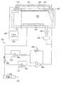
도 1은 본 명세서에서 개시된 실시예에 따라 사용되도록 구성된 예시적인 CVD 반응기의 단면도;1 is a cross-sectional view of an exemplary CVD reactor configured for use in accordance with an embodiment disclosed herein.
도 2는 본 발명의 실시예에 따른 전자 빔 챔버를 나타내는 도면;2 shows an electron beam chamber according to an embodiment of the invention;
도 3은 본 발명의 실시예에 따른 전자 빔 챔버의 일부를 나타내는 도면;3 shows a portion of an electron beam chamber according to an embodiment of the invention;
도 4는 본 발명의 실시예에 따른 피드백 제어 회로를 갖는 전자 빔 챔버를 나타내는 도면.4 illustrates an electron beam chamber having a feedback control circuit in accordance with an embodiment of the present invention.
본 발명의 실시예는 낮은 유전상수의 막을 증착하기 위해 챔버에 하나 이상의 고리형 유기실록산, 하나 이상의 불활성 가스, 및 선택적으로, 하나 이상의 산화 가스를 제공함으로써 실리콘, 산소, 및 탄소를 함유하는 낮은 응력의 낮은 유전 상수의 막을 제공한다. 바람직하게, 낮은 유전상수의 막은 약 3.4 미만의 유전상수를 갖는다. 챔버속으로의 고리형 유기실록산의 전체 유속 대 챔버속으로의 하나 이상의 불활성 가스의 전체 유속의 비는 약 0.10 내지 약 0.20이다. 바람직하게, 캘리포니아, 샌어제이의 프론티어 세미콘덕터로부터 입수가능한 FSM 128L 툴에 의해 측정될 때 막이 약 10MPa 이하의 응력을 갖는 조건에서 막이 증착된다. 보다 바람직하게는, 막은 압축 응력을 갖는다. 압축 응력을 갖는 막은 0 MPa 미만의 응력을 갖는다. 보다 일반적으로, 압축 응력을 제공하는 조건은 평탄한 실리콘 기판상에 컨포멀한 막을 증착함으로써 검출된다. 컨포멀한 막이 증착 이후 아래로 휘는 경우, 즉, 막 에지가 막 중심보다 낮아지는 경우, 프로세스 조건은 압축 응력을 받아들이게 된다.Embodiments of the present invention provide a low stress containing silicon, oxygen, and carbon by providing one or more cyclic organosiloxanes, one or more inert gases, and, optionally, one or more oxidizing gases to the chamber for depositing low dielectric constant films. Provides a film of low dielectric constant. Preferably, the low dielectric constant film has a dielectric constant of less than about 3.4. The ratio of the total flow rate of the cyclic organosiloxane into the chamber to the total flow rate of the one or more inert gases into the chamber is from about 0.10 to about 0.20. Preferably, the film is deposited under conditions that the film has a stress of about 10 MPa or less as measured by an FSM 128L tool available from Frontier Semiconductor, San Jose, California. More preferably, the membrane has a compressive stress. Films with compressive stress have a stress of less than 0 MPa. More generally, conditions providing compressive stress are detected by depositing a conformal film on a flat silicon substrate. When the conformal film bends down after deposition, that is, when the film edge is lower than the film center, the process conditions will accept compressive stress.
고리형 유기실록산은 하나 이상의 실리콘-탄소 결합을 갖는 화합물을 포함한다. 실리콘 원자에 결합된 하나 또는 둘의 알킬기와 교번하는 실리콘 및 산소 원자를 갖는 하나 이상의 링을 포함하는 상업적으로 이용가능한 고리형 유기실록산 화합물이 사용될 수 있다. 예를 들어, 하나 이상의 고리형 유기실록산은 하기의 화합물중 하나 이상일 수 있다.Cyclic organosiloxanes include compounds having one or more silicon-carbon bonds. Commercially available cyclic organosiloxane compounds comprising one or more rings having silicon and oxygen atoms alternating with one or two alkyl groups bonded to silicon atoms can be used. For example, the one or more cyclic organosiloxanes may be one or more of the following compounds.
1,3,5,7-테트라메틸시클로테트라실록산(TMCTS), -(-SiHCH3-O-)4-(고리형)1,3,5,7-tetramethylcyclotetrasiloxane (TMCTS),-(-SiHCH3 -O-)4- (cyclic)
옥타메틸시클로테트라실록산(OMCTS), -(-Si(CH3)2-O-)4-(고리형)Octamethylcyclotetrasiloxane (OMCTS),-(-Si (CH3 )2 -O-)4- (cyclic)
1,3,5,7,9-펜타메틸시클로펜타실록산, -(-SiHCH3-O-)5-(고리형)1,3,5,7,9-pentamethylcyclopentasiloxane,-(-SiHCH3 -O-)5- (cyclic)
헥사메틸시클로트리실록산, -(-Si(CH3)2-O-)3-(고리형)Hexamethylcyclotrisiloxane,-(-Si (CH3 )2 -O-)3- (cyclic)
데카메틸시클로펜타실록산, -(-Si(CH3)2-O-)5-(고리형)Decamethylcyclopentasiloxane,-(-Si (CH3 )2 -O-)5- (cyclic)
하나 이상의 불활성 캐리어 가스가 하나 이상의 고리형 유기실록산과 혼합/섞일 수 있다. 하나 이상의 불활성 가스는 아르곤, 헬륨, 또는 이들의 조합물을 포함할 수 있다.One or more inert carrier gases may be mixed / mixed with one or more cyclic organosiloxanes. One or more inert gases may include argon, helium, or combinations thereof.
본 명세서에서 개시된 임의의 실시예에서, 가스 혼합물은 본질적으로 배제되거나 또는 산소(O2), 오존(O3), 아산화질소(N2O), 일산화탄소(CO), 이산화탄소(CO2), 물(H2O), 및 이들의 혼합물로부터 선택된 하나 이상의 산화 가스를 포함할 수 있다. 일면에서, 산화 가스는 산소 가스이다. 또다른 면에서, 산화 가스는 산소 가스 및 이산화탄소이다. 또다른 면에서, 산화 가스는 오존이다. 오존이 산화 가스로서 사용되는 경우, 오존 발생기는 소스 가스에서 중량당 6% 내지 20%, 통상적으로는 약 15%의 산소를 오존으로 변환시키며, 통상저으로 나머지는 산소가 된다. 그러나, 오존 농도는 사용되는 오존 발생기 장치의 형태 및 원하는 오존의 양에 따라 증가 또는 감소될 수 있다. 하나 이상의 오존 가스가 반응 가스 혼합물에 첨가되어 증착된 막에서 원하는 탄소 함량을 달성하고 반응성을 증가시킬 수 있다.In any of the embodiments disclosed herein, the gas mixture is essentially excluded or contains oxygen (O2 ), ozone (O3 ), nitrous oxide (N2 O), carbon monoxide (CO), carbon dioxide (CO2 ), water (H2 O), and mixtures thereof. In one aspect, the oxidizing gas is oxygen gas. In another aspect, the oxidizing gas is oxygen gas and carbon dioxide. In another aspect, the oxidizing gas is ozone. When ozone is used as the oxidizing gas, the ozone generator converts from 6% to 20%, typically about 15%, oxygen by weight of ozone in the source gas, with the remainder usually being oxygen. However, the ozone concentration can be increased or decreased depending on the type of ozone generator device used and the amount of ozone desired. One or more ozone gases may be added to the reaction gas mixture to achieve the desired carbon content and increase the reactivity in the deposited film.
증착 동안, 고리형 유기실록산 및 하나 이상의 불활성 캐리어 가스의 혼합물에 RF 전력이 인가되어 기판상에 낮은 k 막을 형성할 수 있다. 선택적으로, 하나 이상의 산화 가스가 혼합물에 포함된다. 200 또는 300mm 기판에 제공되는 RF 전력은 약 0.03W/㎠ 내지 약 3.2W/㎠ 사이이며, 이는 200mm 기판에 대해서는 약 10W 내지 약 1,000W의 RF 전력 레벨 그리고 300mm 기판에 대해서는 20W 내지 약 2,250W의 RF 전력 레벨에 해당한다. 바람직하게, RF 전력 레벨은 300mm 기판에 대해 약 200W 내지 약 1,700W 사이이다.During deposition, RF power may be applied to the mixture of cyclic organosiloxane and one or more inert carrier gases to form a low k film on the substrate. Optionally, one or more oxidizing gases are included in the mixture. RF power provided to a 200 or 300 mm substrate is between about 0.03 W / cm 2 to about 3.2 W / cm 2, which is about 10 W to about 1,000 W for a 200 mm substrate and 20 W to about 2,250 W for a 300 mm substrate. Corresponds to the RF power level. Preferably, the RF power level is between about 200 W and about 1700 W for a 300 mm substrate.
막은 약 5 내지 약 30 원자퍼센트(수소 원자 제외) 사이, 바람직하게 약 5 내지 약 20 원자 퍼센트의 탄소 함량을 포함한다. 증착된 막의 탄소 함량은 통상적으로 상다양의 단일-결합 탄화수소를 포함하지 않는 막 구조물의 원자 분석으로 간주된다. 탄소 함량은 양이 상이한 탄소 원자를 제외하고 증착된 막의 탄소원자 퍼센트로 표시된다. 예를 들어, 평균치의 하나의 실리콘 원자, 하나의 산소 원자, 하나의 탄소 원자 및 2개의 수소 원자를 갖는 막은 20 원자 퍼센트(전체 5개 원자당 하나의 탄소 원자)의 탄소 함량, 또는 수소 원자를 제외하고 33 원자 퍼센트(전체 3개의 원자당 하나의 탄소 원자)의 탄소 함량을 갖는다.The membrane comprises a carbon content between about 5 and about 30 atomic percent (excluding hydrogen atoms), preferably between about 5 and about 20 atomic percent. The carbon content of the deposited film is typically considered to be the atomic analysis of the film structure, which does not contain a large variety of single-bonded hydrocarbons. Carbon content is expressed in percent of carbon atoms of the deposited film, excluding carbon atoms of differing amounts. For example, a film having one silicon atom, one oxygen atom, one carbon atom, and two hydrogen atoms of average value may have a carbon content of 20 atomic percent (one carbon atom per five atoms in total), or a hydrogen atom. Except for 33 carbon percent (one carbon atom per three atoms in total).
본 명세서에 개시된 임의의 실시예에서, 낮은 유전상수의 막이 증착된 후에, 상기 막은 막의 유전상수를 감소시키기 위해 전자빔(e-빔)으로 처리될 수 있다. 통상적으로 전자빔 처리는 약 1 내지 20 Kev에서 약 50 내지 약 200 μc/㎠ 사이의 도즈(dose)를 갖는다. 통상적으로 e-빔 전류 범위는 약 1mA 내지 약 40mA이며, 바람직하게는 약 10 내지 20mA이다. 통상적으로 e-빔 처리는 약 10초 내지 약 15 분 동안 약 실온 내지 약 450℃ 사이의 온도에서 작동한다. 일면에서, e-빔 처리 조건은 약 1 미크론의 두께를 갖는 막을 처리하기 위해 약 15 초 내지 약 30초 동안 350℃에서 6kV, 10-18mA 및 50 μc/㎠을 포함한다. 또다른 면에서, e-빔 처리 조건은 약 5000Å의 두께를 갖는 막을 처리하기 위해 약 15 내지 약 30초 동안 350℃에서 4.5kV, 10-18mA 및 50 μc/㎠을 포함한다. 아르곤 또는 수소는 전자 빔 처리 동안 존재할 수 있다. 임의의 e-빔 장치가 사용될 수 있지만, 예시적인 장치로는 어플라이드 머티어리얼스사에서 입수가능한 EBK 챔버가 있다. 낮은 유전상수 막을 증착한 이후 전자 빔으로 낮은 유전상수의 막을 처리하는 것은 막에 보이드를 형성할 수 있는 적어도 소정의 유기 그룹을 막에서 휘발시킨다.In any of the embodiments disclosed herein, after a low dielectric constant film is deposited, the film can be treated with an electron beam (e-beam) to reduce the dielectric constant of the film. Typically the electron beam treatment has a dose between about 50 and about 200 μc / cm 2 at about 1-20 Kev. Typically the e-beam current ranges from about 1 mA to about 40 mA, preferably from about 10 to 20 mA. Typically the e-beam treatment is operated at a temperature between about room temperature and about 450 ° C. for about 10 seconds to about 15 minutes. In one aspect, the e-beam treatment conditions include 6 kV, 10-18 mA and 50 μc / cm 2 at 350 ° C. for about 15 to about 30 seconds to treat a film having a thickness of about 1 micron. In another aspect, the e-beam treatment conditions include 4.5 kV, 10-18 mA and 50 μc / cm 2 at 350 ° C. for about 15 to about 30 seconds to treat a film having a thickness of about 5000 μs. Argon or hydrogen may be present during electron beam processing. Any e-beam device may be used, but an exemplary device is an EBK chamber available from Applied Materials. Treating the low dielectric constant film with an electron beam after depositing the low dielectric constant film volatilizes at least certain organic groups in the film that can form voids in the film.
선택적으로, 또다른 실시예에서, 낮은 유전상수 막을 증착한 후, 상기 막은 막의 유전상수를 감소시키기 위해 어닐링 프로세스로 후(post)-처리된다. 바람직하게, 막은 약 200℃ 내지 약 400℃의 사이의 온도에서 약 2초 내지 약 1 시간, 바람직하게는 약 30분 동안 어닐링된다. 헬륨, 수소, 질소 또는 이들의 혼합물과 같은 비반응성 가스가 100 내지 약 10,000 sccm의 유속으로 주입된다. 챔버 압력은 약 2 Torr 내지 약 10 Torr 사이로 유지된다. RF 전력은 약 13.56MHz의 주파수에서 약 200W 내지 약 1,000W이며, 바람직한 기판 간격은 약 300mils 내지 약 800mils 사이이다.Optionally, in another embodiment, after depositing a low dielectric constant film, the film is post-treated with an annealing process to reduce the dielectric constant of the film. Preferably, the membrane is annealed for about 2 seconds to about 1 hour, preferably about 30 minutes at a temperature between about 200 ° C and about 400 ° C. Non-reactive gases such as helium, hydrogen, nitrogen or mixtures thereof are injected at a flow rate of 100 to about 10,000 sccm. Chamber pressure is maintained between about 2 Torr and about 10 Torr. RF power is between about 200 W and about 1,000 W at a frequency of about 13.56 MHz, with preferred substrate spacing between about 300 mils and about 800 mils.
막은 화학적 기상 증착(CVD)이 가능한 임의의 프로세싱 챔버를 사용하여 증착될 수 있다. 예를 들어, 도 1은 평행판 CVD 프로세싱 챔버(10)의 수직 단면도이다. 챔버(10)는 기판(미도시)으로 프로세스 가스가 분산되는 관통홀을 가지는 가 스 분산 매니폴드(11) 및 고진공 영역(15)을 포함한다. 기판은 기판 지지판 또는 서셉터(12)상에 위치된다. 서셉터(12)는 리프트 모터(14)와 서셉터(12)를 연결하는 지지 스템(13)상에 장착된다. 리프트 모터(14)는 프로세싱 위치와 하부의 기판 장착 위치 사이에서 서셉터(12)를 상승 및 하강시켜 서셉터(12)(및 서셉터(12)의 상부 표면상에 지지되는 기판)가 매니폴드(11)에 가깝게 인접한 상부 프로세싱 위치와 장착/해체 위치 사이에서 제어가능하게 이동할 수 있다. 절연체(17)는 상부 프로세싱 위치에 있는 경우 서셉터(12)와 기판을 둘러싼다.The film may be deposited using any processing chamber capable of chemical vapor deposition (CVD). For example, FIG. 1 is a vertical cross sectional view of a parallel plate
매니폴드(11)로 주입된 가스는 기판 표면에 대해 방사상 균일하게 분산된다. 트로틀 밸브를 갖는 진공 펌프(32)는 매니폴드(24)를 통해 챔버(10)로부터 가스의 배기 속도를 조절한다. 필요하다면 증착 및 캐리어 가스가 가스 라인(18)을 통해 혼합 시스템(19) 및 매니폴드(11)로 흐른다. 일반적으로, 각각의 프로세스 가스 공급 라인(18)은 (i) 챔버속으로 프로세스 가스의 흐름을 자동으로 또는 수동으로 차단하기 위해 사용될 수 있는 안전 차단 밸브(미도시), 및 (ii) 가스 공급 라인(18)을 지나는 가스의 흐름을 측정하기 위한 질량 흐름 제어기(미도시)를 포함한다. 유독성 가스가 프로세스에 사용되는 경우, 통상의 구성에 있는 각각의 가스 공급 라인(18)상에 몇 개의 안전 차단 밸브가 위치된다.The gas injected into the manifold 11 is dispersed uniformly radially with respect to the substrate surface. The
일면에서, 고리형 유기실록산이 약 75 sccm 내지 약 500 sccm의 유속으로 혼합 시스템(19)에 주입된다. 선택적인 하나 이상의 산화 가스는 전체 약 0 sccm 내지 약 200 sccm의 유속을 갖는다. 하나 이상의 불활성 가스는 전체 약 100 sccm 내지 약 5,000 sccm의 유속을 갖는다. 바람직하게, 고리형 유기실리콘 화합물은 옥타메틸클로로테트라실록산이며, 불활성 가스는 헬륨이며, 산화 가스는 산소이다.In one aspect, cyclic organosiloxane is injected into the mixing
상기 개시된 유속은 사용되는 프로세싱 챔버의 크기에 따라 변할 수 있다. 고리형 유기실록산 및 하나 이상의 불활성 가스의 유속은 챔버속으로의 고리형 유기실록산 유속 대 하나 이상의 불활성 가스의 전체 유속의 비율이 약 0.1 내지 약 0.2 사이가 되도록 선택된다.The flow rates disclosed above may vary depending on the size of the processing chamber used. The flow rate of the cyclic organosiloxane and one or more inert gases is selected such that the ratio of the cyclic organosiloxane flow rate to the chamber to the total flow rate of the one or more inert gases is between about 0.1 and about 0.2.
증착 프로세스는 바람직하게 플라즈마 강화 프로세스이다. 플라즈마 강화 프로세스에서, 전형적으로 제어된 플라즈마는 RF 전원장치(25)를 이용하여 가스 분산 매니폴드(11)에 공급된 RF 에너지에 의해 기판 부근에 형성된다. 선택적으로, RF 전력은 서셉터(12)에 공급될 수 있다. 증착 챔버로의 RF 전력은 기판 가열을 감소시키고 증착된 막의 보다 큰 다공성을 조장하기 위해 순화되거나 펄스화될 수 있다.The deposition process is preferably a plasma enhancement process. In the plasma intensification process, typically a controlled plasma is formed near the substrate by the RF energy supplied to the
RF 전원장치(25)는 약 0.01 MHz 내지 300 MHz 사이에서 단일 주파수 RF 전력을 공급할 수 있다. 바람직하게, RF 주파수는 고진공 영역(15)으로 주입되는 반응성 종의 분해를 강화시키기 위해 혼합, 동시 주파수들을 사용하여 전달될 수 있다. 일면에서, 혼합 주파수는 약 12 kHz의 낮은 주파수 및 약 13.567 mHz의 높은 주파수이다. 또다른 면에서, 낮은 주파수 범위는 약 300 Hz 내지 약 1,000 kHz 사이이며, 높은 주파수 범위는 약 5 mHz 내지 약 50 mHz 사이이다. 바람직하게, 낮은 주파수 전력 레벨은 약 150W이다. 바람직하게, 높은 주파수 전력 레벨은 약 200W 내지 약 750W, 보다 바람직하게는 약 200W 내지 약 400W이다.The
증착 동안, 기판은 약 -20℃ 내지 약 500℃, 바람직하게는 약 100℃ 내지 약 450℃ 사이의 온도에서 유지된다. 증착 압력은 전형적으로 약 2 Torr 내지 약 10 Torr, 바람직하게는 약 4 Torr 내지 약 7 Torr 사이이다. 증착 속도는 전형적으로 약 3,000Å/min 내지 약 15,000Å/min이다.During deposition, the substrate is maintained at a temperature between about -20 ° C and about 500 ° C, preferably between about 100 ° C and about 450 ° C. Deposition pressures are typically between about 2 Torr and about 10 Torr, preferably between about 4 Torr and about 7 Torr. Deposition rates are typically from about 3,000 kPa / min to about 15,000 kPa / min.
산화 가스의 추가적인 분해가 요구되는 경우, 선택적인 마이크로파 챔버(28)가 프로세싱 챔버(10)로 가스가 진입하기 이전에 산화 가스에 약 50와트 내지 약 6,000와트 사이의 전력을 입력하기 위해 사용될 수 있다. 추가적인 마이크로파 전력은 산화 가스와 반응하기 이전에 유기실리콘 화합물의 과도한 분해를 방지할 수 있다. 마이크로파 전력이 산화 가스에 부가되는 경우 유기실리콘 화합물 및 산화 가스에 대한 개별 통로를 가지는 가스 분산판(미도시)이 바람직하다.If further decomposition of the oxidizing gas is desired, an
통상적으로, 임의의 또는 전체 챔버 라이닝, 분산 매니폴드(11), 서셉터(12) 및 다양한 다른 반응기 하드웨어가 알루미늄 또는 산화 알루미늄과 같은 물질로 구성될 수 있다. 이러한 CVD 반응기의 예로는, 본 명세서에서 참조되는 "열적 CVD/PECVD 반응기 및 실리콘이산화물의 열적 화학적 기상 증착 및 인슈트 다단계 평탄화 프로세스"란 명칭의 US 특허 No. 5,000,113호에 개시되어 있다.Typically, any or all chamber linings, dispersion manifolds 11,
시스템 제어기(34)는 모터(14), 가스 혼합 시스템(19), 및 제어 라인(36)에 의해 접속되는 RF 전원장치(25)를 제어한다. 시스템 제어기(34)는 CVD 반응기의 동작을 제어하며 전형적으로 하드 디스크 드라이브, 플로피 디스크 드라이브, 및 카드 랙을 포함한다. 카드 랙은 단일 보드 컴퓨터(SBC), 아날로그 및 디지털 입/출력 보드, 인터페이스 보드 및 스텝퍼 모터 제어기 보드를 포함한다. 시스템 제어기(34)는 보드, 카드 케이지 및 커넥터 치수 및 형태를 한정하는 VME(Versa Modular Europeans) 스탠다드를 따른다. 또한, VME 스탠다드는 16-비트 데이터 버스 및 24-비트 어드레스 버스를 갖는 버스 구조를 한정한다. 시스템 제어기(34)는 하드 디스크 드라이브(38)상에 저장된 컴퓨터 프로그램의 제어하에서 동작한다.The
상기 CVD 시스템 설명은 주로 도시를 위한 것으로, ECR(electrode cyclotron resonance) 플라즈마 CVD 장치, 유도-결합된 RF 고밀도 플라즈마 장치 등과 같은 다른 CVD 장비가 사용될 수도 있다. 부가적으로, 서셉터 설계, 히터 설계, RF 전력 접속기의 위치 및 다른 것들의 변형과 같이 상기 개시된 시스템의 변형이 가능하다. 예를 들어, 기판은 저항성 가열된 서셉터에 의해 지지되고 가열될 수 있다.The above CVD system description is primarily for illustration, and other CVD equipment may be used, such as an electrode cyclotron resonance (ECR) plasma CVD apparatus, an inductively-coupled RF high density plasma apparatus, and the like. Additionally, variations of the disclosed system are possible, such as susceptor design, heater design, location of RF power connectors, and others. For example, the substrate can be supported and heated by a resistive heated susceptor.
일단 막이 증착되면, 기판은 추가적인 프로세싱, 예를 들어 경화(curing)를 위해 전자 빔(e-빔) 장치로 이송될 수 있다. 기판은 진공을 깨뜨리거나 또는 진공하에서, 즉, 임의의 진공을 깨뜨리지 않고 이송될 수 있다. 도 2는 본 발명의 실시예에 따른 e-빔 챔버(200)를 나타낸다. e-빔 챔버(200)는 진공 챔버(220), 대면적 캐소드(222), 영전계(field-free) 영역(238)에 위치된 타겟 평면(230), 및 타겟 평면(230)과 대면적 캐소드(222) 사이에 위치된 그리드 애노드(226)를 포함한다. e-빔 챔버(200)는 대면적 캐소드(222)와 그리드 애노드(226)를 절연시키는 고전압 절연체(224), 진공 챔버(220) 외측에 위치된 캐소드 커버 절연체(228), 진공 챔버(220) 내부 압력을 제어하는 가변 누설 밸브(232), 대면적 캐소드(222)에 결합된 가변 고전압 전원장치(229), 및 그리드 애노드(226)에 결합된 가변 저압 전원장치(231)를 더 포함한다.Once the film is deposited, the substrate can be transferred to an electron beam (e-beam) device for further processing, for example curing. The substrate may be transported under a vacuum or under vacuum, ie without breaking any vacuum. 2 shows an
동작시, 전자 빔에 노출되는 기판(미도시)은 타겟 평면(230)상에 위치된다. 진공 챔버(220)는 대기압에서 약 1 mTorr 내지 약 200 mTorr 범위의 압력으로 펌프된다. 배기 압력은 약 0.1 mTorr로 압력을 제어할 수 있는 가변 비율 누설 밸브(232)에 의해 제어된다. 일반적으로 전자 빔은 고전압 전원장치(229)에 의해 대면적 캐소드(222)에 공급되는 충분히 높은 전압에서 발생된다. 전압 범위는 약 -500볼트 내지 약 30,000 볼트 이상일 수 있다. 고전압 전원장치(229)는, 뉴욕, 히크빌의 Bertan에 의해 제조된 Bertan Model #105-30R 또는 뉴욕, 허퍼지의 Spellman High Voltage Electronics Corp.에 의해 제조된 Spellman Model #SL30N-1200X 258일 수 있다. 가변 저전압 전원장치(231)은 그리드 애노드에 대면적 캐소드(222)에 인가된 전압에 대해 포지티브인 전압을 공급한다. 상기 전압은 대면적 캐소드(222)로부터의 전자 방출을 제어하는데 사용된다. 가변 저전압 전원장치(231)는 Easton, Pa의 Acopian으로부터 이용가능한 Acopian Model #150PT12 전원장치일 수 있다.In operation, a substrate (not shown) exposed to the electron beam is positioned on the
전자 방출을 개시하기 위해, 그리드 애노드(226)와 타겟 평면(230) 사이의 영전계 영역(238)의 가스는 이온화되어야 하면, 이는 자연스럽게 발생하는 감마 광선의 결과로서 야기될 수 있다. 또한 전자 방출은 고전압 스파이크 갭에 의해 진공 챔버(220) 내부에서 인공적으로 개시될 수 있다. 이러한 개시 이온화가 발생되면, 포지티브 이온(342)(도 3에 도시됨)이 그리드 애노드(226)에 인가된 약 0 내지 약 -200볼트 정도의 약한 네거티브 전압에 의해 그리드 애노드(226)에 부착된다. 이러한 포지티브 이온(342)은 가속 전계 영역(236)을 통과하여 대면적 캐소드(22)와 그리드 애노드(226) 사이에 배치되며 대면적 캐소드(222)에 인가되는 고전압의 결과로서 대면적 캐소드(222)를 향해 가속된다. 대면적 캐소드(222)를 가격함에 따라, 이들 고-에너지 이온은 2차 전자(344)를 형성하여 그리드 애노드(226)를 향해 다시 가속된다. 캐소드 표면에 일반적으로 수직으로 이동하는 이들 전자(344)의 일부는 그리드 애노드(226)를 가격하지만, 상기 전자(344)의 대부분은 그리드 애노드(226)를 통과하여 타겟 평면(230)으로 이동한다. 그리드 애노드(226)는 바람직하게 대면적 캐소드(222)에 의해 방출되는 전자의 평균 자유 경로 보다 작은 간격에 위치된다. 예를 들어, 그리드 애노드(226)는 대면적 캐소드(222)로부터 약 4mm 미만에 바람직하게 위치된다. 그리드 애노드(226)와 대면적 캐소드(222) 사이의 짧은 간격으로 인해, 그리드 애노드(226)와 대면적 캐소드(222) 사이의 가속 전계 영역(236)에서 이온화가 없거나 또는 임의의 경우 최소화된다.In order to initiate electron emission, the gas in the field of
종래의 가스 방전 장치에서, 전자는 가속 전계 영역에 포지티브 이온을 추가로 발생시켜, 대면적 캐소드(222)에 부착되어 전자 방출을 보다 더 형성한다. 방전은 불안정한 고전압 브레이크다운으로 쉽게 애벌런치될 수 있다. 그러나, 본 발명의 실시예에 따라, 그리드 애노드(226) 외측에 형성된 이온(342)은 그리드 애노드(226)에 인가된 전압에 의해 제어된다(반발 또는 유인된다). 다른 말로, 전자 방출은 그리드 애노드(226) 상의 전압이 변함에 따라 연속적으로 제어될 수 있다. 선택적으로, 전자 방출은 타겟 평면(230)과 대면적 캐소드(222) 사이의 이온화 영역에서 분자의 수를 높이거나 또는 낮출수 있도록 구성된 가변 누설 밸브(232)에 의해 제어될 수 있다. 전자 방출은 그리드 애노드(226)에 포지티브 전압을 인가함으로써, 즉, 그리드 애노드 전압이 리드 애노드(226)와 타겟 평면(230) 사이의 공 간에 형성된 임의의 포지티브 이온 종의 에너지를 초과하는 경우 완전히 턴오프된다.In a conventional gas discharge device, electrons further generate positive ions in the accelerated electric field region, and are attached to the
도 4는 피드백 제어 회로(400)를 갖는 e-빔 챔버(200)를 나타낸다. 소정의 분야에 있어, 상이한 전자 빔 에너지에서 일정한 빔 전류를 제공하는 것이 바람직하다. 예를 들어, 기판상에 형성된 막의 상부층(하부층은 아님)을 노출 또는 경화시키는 것이 바람직하다. 이는 대부분의 전자들이 막의 상부층에 흡수되도록 전자 빔 에너지를 낮춤으로써 달성될 수 있다. 상부층의 경화에 이어, 막의 전체 두께가 경화되는 것이 바람직하다. 이는 막을 대해 완전히 천공되도록 전자 빔의 가속 전압을 상승시킴으로 써 달성된다. 피드백 제어 회로(400)는 가속 전압에서의 변화에 따라 일정한 빔 전류를 유지하도록 구성된다. 피드백 제어 회로(400)는 적분기(integrator)(466)를 포함한다. 빔 전류는 타겟 평면(230)과 적분기(466) 사이에 위치된 센스 레지스터(490)를 통해 샘플링된다. 또한 빔 전류는 빔의 일부가 차단됨에 따라 그리드 애노드(236)에서 샘플링될 수 있다. 2개의 단일 게인 전압 팔로워(492)(follower)는 센스 레지스터(490)에 대해 얻어진 신호를 버퍼링하고 가변 레지스터(494)를 갖는 증폭기(496)에 이를 공급한다. 상기 증폭기의 출력은 빔전류의 증가가 그리드 애노드(226) 상의 바이어스 전압을 감소시키고 대면적 캐소드(222)로부터의 빔 전류를 감소시키도록 그리드 애노드(226)상의 전압을 제어한다. 증폭기(496) 게인은 가변 레지스터(494)에 의해 제어되어, 가속 전압 변화에 의해 야기되는 빔 전류의 임의의 변화가 바이어스 전압에서의 변화에 의해 중화되어 타겟에서 일정한 빔 전류를 유지할 수 있다. 선택적으로, 증폭기(496)의 출력 은 이온화 영역(238)의 압력을 상승 또는 낮춤으로써 빔 전류의 변화를 중화시키기 위해 전압 제어 가변 비율 누설 밸브(232)에 결합될 수 있다. 또한,빔 전류 제어의 폭넓은 범위는 가변 누설 밸브(232)와 그리드 애노드(226) 양쪽에 피드백 신호를 이용함으로써 제공될 수 있다. e-빔 챔버(200)의 다른 상세한 설명은 본 발명과 일치하지 않는 정도로 참조되는 Electron Vision Corporation(본 발명의 양수인에 의해 현재 소유됨)에 양도된 William R. Livesay에 의해 발행된 "대면적의 균일한 전자 소스"란 명칭의 US 특허 No. 5,003,178호에 개시되어 있다.4 shows an
실시예들Examples : :
하기의 실시예들은 본 발명의 낮은 유전성 막을 나타낸다. 막은 통합된 프로세싱 플랫폼의 일부인 화학적 기상 증착 챔버를 이용하여 증착된다. 특히, 상기 막은 캘리포니아 산타클라라의 Applied Materials Inc.로부터 입수가능한 Producer
실시예Example 1 One
낮은 유전상수 막은 약 5 Torr의 챔버 압력 및 약 350의 기판 온도에서 하기의 반응성 가스로부터 300mm 기판상에 증착된다.A low dielectric constant film is deposited on a 300 mm substrate from the following reactive gases at a chamber pressure of about 5 Torr and a substrate temperature of about 350.
약 100 sccm에서 옥타메틸시클로테트라실록산(OMCTS),Octamethylcyclotetrasiloxane (OMCTS) at about 100 sccm,
약 50 sccm에서 산소Oxygen at about 50 sccm
약 1,000 sccm에서 헬륨Helium at about 1,000 sccm
기판은 가스 분산 샤워헤드로부터 450mils에 위치된다. 13.56MH의 주파수에서 약 500W의 전력 레벨 및 350kHz의 주파수에서 약 150W의 전력 레벨이 막의 플라즈마 강화 증착을 위해 샤워헤드에 인가된다. 막은 약 3,510Å/min의 속도로 증착되며, 0.1MHz에서 측정된 약 3.35의 유전상수(k)를 갖는다. 막은 -67.21 MPa의 압축 응력을 갖는다.The substrate is located at 450 mils from the gas dispersion showerhead. A power level of about 500 W at a frequency of 13.56 MH and a power level of about 150 W at a frequency of 350 kHz is applied to the showerhead for plasma enhanced deposition of the film. The film is deposited at a rate of about 3,510 mA / min and has a dielectric constant (k) of about 3.35 measured at 0.1 MHz. The membrane has a compressive stress of -67.21 MPa.
실시예Example 2 2
낮은 유전상수 막이 약 5 Torr의 챔버 압력 및 약 350℃의 기판 온도에서 하기의 반응성 가스로부터 300mm 기판상에 증착된다.A low dielectric constant film is deposited on a 300 mm substrate from the following reactive gases at a chamber pressure of about 5 Torr and a substrate temperature of about 350 ° C.
약 150 sccm에서 옥타메틸시클로테트라실록산(OMCTS),Octamethylcyclotetrasiloxane (OMCTS) at about 150 sccm,
약 75 sccm에서 산소Oxygen at about 75 sccm
약 1,000 sccm에서 헬륨Helium at about 1,000 sccm
기판은 가스 분산 샤워헤드로부터 450mils에 위치된다. 13.56MH의 주파수에서 약 500W의 전력 레벨 및 350kHz의 주파수에서 약 150W의 전력 레벨이 막의 플라즈마 강화 증착을 위해 샤워헤드에 인가된다. 막은 약 5,754Å/min의 속도로 증착되며, 0.1MHz에서 측정된 약 3.15의 유전상수(k)를 갖는다. 막은 -13.34 MPa의 압축 응력을 갖는다.The substrate is located at 450 mils from the gas dispersion showerhead. A power level of about 500 W at a frequency of 13.56 MH and a power level of about 150 W at a frequency of 350 kHz is applied to the showerhead for plasma enhanced deposition of the film. The film is deposited at a rate of about 5,754 mA / min and has a dielectric constant (k) of about 3.15 measured at 0.1 MHz. The membrane has a compressive stress of -13.34 MPa.
실시예Example 3 3
낮은 유전상수 막이 약 5 Torr의 챔버 압력 및 약 350℃의 기판 온도에서 하 기의 반응성 가스로부터 300mm 기판상에 증착된다.A low dielectric constant film is deposited on a 300 mm substrate from the reactive gas below at a chamber pressure of about 5 Torr and a substrate temperature of about 350 ° C.
약 200 sccm에서 옥타메틸시클로테트라실록산(OMCTS),Octamethylcyclotetrasiloxane (OMCTS) at about 200 sccm,
약 100 sccm에서 산소Oxygen at about 100 sccm
약 1,000 sccm에서 헬륨Helium at about 1,000 sccm
기판은 가스 분산 샤워헤드로부터 450mils에 위치된다. 13.56MH의 주파수에서 약 500W의 전력 레벨 및 350kHz의 주파수에서 약 150W의 전력 레벨이 막의 플라즈마 강화 증착을 위해 샤워헤드에 인가된다. 막은 약 6,899Å/min의 속도로 증착되며, 0.1MHz에서 측정된 약 2.98의 유전상수(k)를 갖는다. 막은 7.29 MPa의 인장 응력을 갖는다.The substrate is located at 450 mils from the gas dispersion showerhead. A power level of about 500 W at a frequency of 13.56 MH and a power level of about 150 W at a frequency of 350 kHz is applied to the showerhead for plasma enhanced deposition of the film. The film is deposited at a rate of about 6,899 mA / min and has a dielectric constant (k) of about 2.98 measured at 0.1 MHz. The membrane has a tensile stress of 7.29 MPa.
비교compare실시예Example 1 One
낮은 유전상수 막이 약 5 Torr의 챔버 압력 및 약 350℃의 기판 온도에서 하기의 반응성 가스로부터 300mm 기판상에 증착된다.A low dielectric constant film is deposited on a 300 mm substrate from the following reactive gases at a chamber pressure of about 5 Torr and a substrate temperature of about 350 ° C.
약 215 sccm에서 옥타메틸시클로테트라실록산(OMCTS),Octamethylcyclotetrasiloxane (OMCTS) at about 215 sccm,
약 160 sccm에서 산소Oxygen at about 160 sccm
약 1,000 sccm에서 헬륨Helium at about 1,000 sccm
기판은 가스 분산 샤워헤드로부터 450mils에 위치된다. 13.56MH의 주파수에서 약 500W의 전력 레벨 및 350kHz의 주파수에서 약 150W의 전력 레벨이 막의 플라즈마 강화 증착을 위해 샤워헤드에 인가된다. 막은 약 8,285Å/min의 속도로 증착되며, 0.1MHz에서 측정된 약 2.9의 유전상수(k)를 갖는다. 막은 24.72 MPa의 인장 응력을 갖는다.The substrate is located at 450 mils from the gas dispersion showerhead. A power level of about 500 W at a frequency of 13.56 MH and a power level of about 150 W at a frequency of 350 kHz is applied to the showerhead for plasma enhanced deposition of the film. The film is deposited at a rate of about 8,285 mA / min and has a dielectric constant (k) of about 2.9 measured at 0.1 MHz. The membrane has a tensile stress of 24.72 MPa.
비교compare실시예Example 2 2
낮은 유전상수 막이 약 5 Torr의 챔버 압력 및 약 350℃의 기판 온도에서 하기의 반응성 가스로부터 300mm 기판상에 증착된다.A low dielectric constant film is deposited on a 300 mm substrate from the following reactive gases at a chamber pressure of about 5 Torr and a substrate temperature of about 350 ° C.
약 253 sccm에서 옥타메틸시클로테트라실록산(OMCTS),Octamethylcyclotetrasiloxane (OMCTS) at about 253 sccm,
약 125 sccm에서 산소Oxygen at about 125 sccm
약 1,000 sccm에서 헬륨Helium at about 1,000 sccm
기판은 가스 분산 샤워헤드로부터 450mils에 위치된다. 13.56MH의 주파수에서 약 500W의 전력 레벨 및 350kHz의 주파수에서 약 150W의 전력 레벨이 막의 플라즈마 강화 증착을 위해 샤워헤드에 인가된다. 막은 약 8,041Å/min의 속도로 증착되며, 0.1MHz에서 측정된 약 2.83의 유전상수(k)를 갖는다. 막은 20.03 MPa의 인장 응력을 갖는다.The substrate is located at 450 mils from the gas dispersion showerhead. A power level of about 500 W at a frequency of 13.56 MH and a power level of about 150 W at a frequency of 350 kHz is applied to the showerhead for plasma enhanced deposition of the film. The film is deposited at a rate of about 8,041 mA / min and has a dielectric constant (k) of about 2.83 measured at 0.1 MHz. The membrane has a tensile stress of 20.03 MPa.
비교compare실시예Example 3 3
낮은 유전상수 막이 약 5 Torr의 챔버 압력 및 약 350℃의 기판 온도에서 하기의 반응성 가스로부터 300mm 기판상에 증착된다.A low dielectric constant film is deposited on a 300 mm substrate from the following reactive gases at a chamber pressure of about 5 Torr and a substrate temperature of about 350 ° C.
약 302 sccm에서 옥타메틸시클로테트라실록산(OMCTS),Octamethylcyclotetrasiloxane (OMCTS) at about 302 sccm,
약 160 sccm에서 산소Oxygen at about 160 sccm
약 1,000 sccm에서 헬륨Helium at about 1,000 sccm
기판은 가스 분산 샤워헤드로부터 450mils에 위치된다. 13.56MH의 주파수에서 약 500W의 전력 레벨 및 350kHz의 주파수에서 약 150W의 전력 레벨이 막의 플라즈마 강화 증착을 위해 샤워헤드에 인가된다. 막은 약 8,556Å/min의 속도로 증착되며, 0.1MHz에서 측정된 약 2.78의 유전상수(k)를 갖는다. 막은 28.77 MPa의 인장 응력을 갖는다.The substrate is located at 450 mils from the gas dispersion showerhead. A power level of about 500 W at a frequency of 13.56 MH and a power level of about 150 W at a frequency of 350 kHz is applied to the showerhead for plasma enhanced deposition of the film. The film is deposited at a rate of about 8,556 mA / min and has a dielectric constant (k) of about 2.78 measured at 0.1 MHz. The membrane has a tensile stress of 28.77 MPa.
실시예Example 4 4
낮은 유전상수 막이 약 5 Torr의 챔버 압력 및 약 350℃의 기판 온도에서 하기의 반응성 가스로부터 300mm 기판상에 증착된다.A low dielectric constant film is deposited on a 300 mm substrate from the following reactive gases at a chamber pressure of about 5 Torr and a substrate temperature of about 350 ° C.
약 215 sccm에서 옥타메틸시클로테트라실록산(OMCTS),Octamethylcyclotetrasiloxane (OMCTS) at about 215 sccm,
약 1,000 sccm에서 헬륨Helium at about 1,000 sccm
기판은 가스 분산 샤워헤드로부터 300mils에 위치된다. 13.56MH의 주파수에서 약 400W의 전력 레벨 및 350kHz의 주파수에서 약 150W의 전력 레벨이 막의 플라즈마 강화 증착을 위해 샤워헤드에 인가된다. 막은 약 4,275Å/min의 속도로 증착되며, 0.1MHz에서 측정된 약 3.12의 유전상수(k)를 갖는다. 막은 -4.16 MPa의 압축 응력을 갖는다.The substrate is located at 300 mils from the gas dispersion showerhead. A power level of about 400 W at a frequency of 13.56 MH and a power level of about 150 W at a frequency of 350 kHz is applied to the showerhead for plasma enhanced deposition of the film. The film is deposited at a rate of about 4,275 mA / min and has a dielectric constant (k) of about 3.12 measured at 0.1 MHz. The membrane has a compressive stress of -4.16 MPa.
실시예Example 5 5
낮은 유전상수 막이 약 5 Torr의 챔버 압력 및 약 350℃의 기판 온도에서 하기의 반응성 가스로부터 300mm 기판상에 증착된다.A low dielectric constant film is deposited on a 300 mm substrate from the following reactive gases at a chamber pressure of about 5 Torr and a substrate temperature of about 350 ° C.
약 215 sccm에서 옥타메틸시클로테트라실록산(OMCTS),Octamethylcyclotetrasiloxane (OMCTS) at about 215 sccm,
약 1,500 sccm에서 헬륨Helium at about 1500 sccm
기판은 가스 분산 샤워헤드로부터 300mils에 위치된다. 13.56MH의 주파수에서 약 400W의 전력 레벨 및 350kHz의 주파수에서 약 150W의 전력 레벨이 막의 플라즈마 강화 증착을 위해 샤워헤드에 인가된다. 막은 약 4,942Å/min의 속도로 증착되며, 0.1MHz에서 측정된 약 3.07의 유전상수(k)를 갖는다. 막은 2.45 MPa의 인장 응력을 갖는다.The substrate is located at 300 mils from the gas dispersion showerhead. A power level of about 400 W at a frequency of 13.56 MH and a power level of about 150 W at a frequency of 350 kHz is applied to the showerhead for plasma enhanced deposition of the film. The film is deposited at a rate of about 4,942 mA / min and has a dielectric constant (k) of about 3.07 measured at 0.1 MHz. The membrane has a tensile stress of 2.45 MPa.
비교compare실시예Example 4 4
낮은 유전상수 막이 약 5 Torr의 챔버 압력 및 약 350℃의 기판 온도에서 하기의 반응성 가스로부터 300mm 기판상에 증착된다.A low dielectric constant film is deposited on a 300 mm substrate from the following reactive gases at a chamber pressure of about 5 Torr and a substrate temperature of about 350 ° C.
약 215 sccm에서 옥타메틸시클로테트라실록산(OMCTS),Octamethylcyclotetrasiloxane (OMCTS) at about 215 sccm,
약 1,000 sccm에서 헬륨Helium at about 1,000 sccm
기판은 가스 분산 샤워헤드로부터 300mils에 위치된다. 13.56MH의 주파수에서 약 300W의 전력 레벨 및 350kHz의 주파수에서 약 150W의 전력 레벨이 막의 플라즈마 강화 증착을 위해 샤워헤드에 인가된다. 막은 약 4,062Å/min의 속도로 증착되며, 0.1MHz에서 측정된 약 2.96의 유전상수(k)를 갖는다. 막은 20.25 MPa의 인장 응력을 갖는다.The substrate is located at 300 mils from the gas dispersion showerhead. A power level of about 300 W at a frequency of 13.56 MH and a power level of about 150 W at a frequency of 350 kHz is applied to the showerhead for plasma enhanced deposition of the film. The film is deposited at a rate of about 4,062 mA / min and has a dielectric constant (k) of about 2.96 measured at 0.1 MHz. The membrane has a tensile stress of 20.25 MPa.
비교compare실시예Example 5 5
낮은 유전상수 막이 약 5 Torr의 챔버 압력 및 약 350℃의 기판 온도에서 하기의 반응성 가스로부터 300mm 기판상에 증착된다.A low dielectric constant film is deposited on a 300 mm substrate from the following reactive gases at a chamber pressure of about 5 Torr and a substrate temperature of about 350 ° C.
약 215 sccm에서 옥타메틸시클로테트라실록산(OMCTS),Octamethylcyclotetrasiloxane (OMCTS) at about 215 sccm,
약 1,000 sccm에서 헬륨Helium at about 1,000 sccm
기판은 가스 분산 샤워헤드로부터 300mils에 위치된다. 13.56MH의 주파수에서 약 400W의 전력 레벨 및 350kHz의 주파수에서 약 150W의 전력 레벨이 막의 플라즈마 강화 증착을 위해 샤워헤드에 인가된다. 막은 약 5,376Å/min의 속도로 증착되며, 0.1MHz에서 측정된 약 3.01의 유전상수(k)를 갖는다. 막은 14.62 MPa의 인장 응력을 갖는다.The substrate is located at 300 mils from the gas dispersion showerhead. A power level of about 400 W at a frequency of 13.56 MH and a power level of about 150 W at a frequency of 350 kHz is applied to the showerhead for plasma enhanced deposition of the film. The film is deposited at a rate of about 5,376 mA / min and has a dielectric constant (k) of about 3.01 measured at 0.1 MHz. The membrane has a tensile stress of 14.62 MPa.
실시예 1-3 및 비교 실시예 1-3은 OMCTS, 헬륨 및 산소가 포함된 가스 혼합물로부터 낮은 유전상수의 막을 증착하는데 사용되는 프로세싱 조건을 나타낸다. 실시예 1-3의 막은 3.4 미만의 유전상수 및 <10 MPa의 응력을 갖는다. 비교 실시예 1 및 2의 막은 3.4 미만의 유전상수를 갖는다. 그러나, 비교 실시예 1 및 2의 막은 20MPa 이상의 인장 응력을 갖는다. 본 명세서에서 정의된 바와 같이, 인장 응력을 갖는 막은 FSM 128L 툴로 측정된 바와 같이, 0MPa 이상의 응력을 갖는 막이다.Examples 1-3 and Comparative Examples 1-3 show the processing conditions used to deposit low dielectric constant films from gas mixtures containing OMCTS, helium and oxygen. The membrane of Examples 1-3 has a dielectric constant of less than 3.4 and a stress of <10 MPa. The membranes of Comparative Examples 1 and 2 have a dielectric constant of less than 3.4. However, the films of Comparative Examples 1 and 2 have a tensile stress of 20 MPa or more. As defined herein, a film having a tensile stress is a film having a stress of 0 MPa or more, as measured by the FSM 128L tool.
실시예 4-5 및 비교 실시예 3 및 4는 OMCTS 및 헬륨이 포함된 가스 혼합물로부터 낮은 유전상수의 막을 증착하는데 사용된 프로세싱 조건을 나타낸다. 실시예 4-5의 막은 3.4 미만의 유전상수 및 <3MPa의 응력을 갖는다. 비교 실시예 3 및 4의 막은 3.4 미만의 유전상수를 갖는다. 그러나, 비교 실시예 3 및 4의 막은 14MPa 이상의 인장응력을 갖는다.Examples 4-5 and Comparative Examples 3 and 4 show the processing conditions used to deposit low dielectric constant films from gas mixtures containing OMCTS and helium. The membrane of Examples 4-5 has a dielectric constant of less than 3.4 and a stress of <3 MPa. The membranes of Comparative Examples 3 and 4 have a dielectric constant of less than 3.4. However, the membranes of Comparative Examples 3 and 4 have a tensile stress of 14 MPa or more.
비교 실시예 1-5에서 보다 실시예 1-5에서 OMCTS의 유속 대 불활성 캐리어 가스 헬륨의 유속의 낮은 비율은 실시예 3 및 5의 낮은 인장 응력 및 실시예 1, 2 및 4의 압축 응력에 기여하는 것으로 여겨진다. 실시예 1-5는 0.10 내지 0.20의 OMCTS/헬륨 유속 비를 갖는 반면, 비교 실시예들은 0.215 내지 0.302의 OMCTS/헬륨의 비를 갖는다.The lower ratio of the flow rate of OMCTS to the flow rate of the inert carrier gas helium in Examples 1-5 than in Comparative Examples 1-5 contributes to the low tensile stress of Examples 3 and 5 and the compressive stress of Examples 1, 2 and 4 It is believed to be. Examples 1-5 have an OMCTS / helium flow rate ratio of 0.10 to 0.20, while comparative examples have an OMCTS / helium ratio of 0.215 to 0.302.
또한 본 명세서에서 개시된 약 2 Torr 내지 10 Torr의 챔버 압력에서 가스 혼합물의 반응은 본 명세서에서 개시된 막의 압축 또는 낮은 인장 응력 및 <3.4의 유전 상수에 기여하는 것으로 여겨진다.It is also believed that the reaction of the gas mixture at a chamber pressure of about 2 Torr to 10 Torr disclosed herein contributes to the compressive or low tensile stress of the membranes disclosed herein and a dielectric constant of <3.4.
지금까지 본 발명의 바람직한 실시예에 관해 설명했지만, 하기의 청구범위에 한정된 본 발명의 기본 정신 및 범주를 이탈하지 않는 다른 실시예들이 고안될 수 있다.While the preferred embodiments of the present invention have been described so far, other embodiments may be devised without departing from the spirit and scope of the invention as defined in the following claims.
Claims (20)
Translated fromKoreanApplications Claiming Priority (2)
| Application Number | Priority Date | Filing Date | Title |
|---|---|---|---|
| US10/642,081US20050037153A1 (en) | 2003-08-14 | 2003-08-14 | Stress reduction of sioc low k films |
| US10/642,081 | 2003-08-14 |
Publications (1)
| Publication Number | Publication Date |
|---|---|
| KR20060059913Atrue KR20060059913A (en) | 2006-06-02 |
Family
ID=34136527
Family Applications (1)
| Application Number | Title | Priority Date | Filing Date |
|---|---|---|---|
| KR1020057025091ACeasedKR20060059913A (en) | 2003-08-14 | 2004-08-02 | SIOC How to reduce the stress of low SO film |
Country Status (5)
| Country | Link |
|---|---|
| US (1) | US20050037153A1 (en) |
| KR (1) | KR20060059913A (en) |
| CN (1) | CN100541735C (en) |
| TW (1) | TWI325897B (en) |
| WO (1) | WO2005020310A1 (en) |
Cited By (5)
| Publication number | Priority date | Publication date | Assignee | Title |
|---|---|---|---|---|
| US7601651B2 (en) | 2006-03-31 | 2009-10-13 | Applied Materials, Inc. | Method to improve the step coverage and pattern loading for dielectric films |
| KR100939593B1 (en)* | 2006-11-21 | 2010-02-01 | 어플라이드 머티어리얼스, 인코포레이티드 | A method of minimizing wet etch undercuts and providing a void seal of the lowest dielectrics with an index of less than 2.5. |
| US7780865B2 (en) | 2006-03-31 | 2010-08-24 | Applied Materials, Inc. | Method to improve the step coverage and pattern loading for dielectric films |
| US8445075B2 (en) | 2006-03-31 | 2013-05-21 | Applied Materials, Inc. | Method to minimize wet etch undercuts and provide pore sealing of extreme low k (k<2.5) dielectrics |
| KR20190049893A (en)* | 2016-09-29 | 2019-05-09 | 램 리써치 코포레이션 | Low Temperature Formation of High-Quality Silicon Oxide Films in Semiconductor Device Manufacturing |
Families Citing this family (13)
| Publication number | Priority date | Publication date | Assignee | Title |
|---|---|---|---|---|
| US6913992B2 (en) | 2003-03-07 | 2005-07-05 | Applied Materials, Inc. | Method of modifying interlayer adhesion |
| US7638859B2 (en) | 2005-06-06 | 2009-12-29 | Taiwan Semiconductor Manufacturing Co., Ltd. | Interconnects with harmonized stress and methods for fabricating the same |
| US7381659B2 (en)* | 2005-11-22 | 2008-06-03 | International Business Machines Corporation | Method for reducing film stress for SiCOH low-k dielectric materials |
| US20080050932A1 (en)* | 2006-08-23 | 2008-02-28 | Applied Materials, Inc. | Overall defect reduction for PECVD films |
| US7598183B2 (en)* | 2006-09-20 | 2009-10-06 | Applied Materials, Inc. | Bi-layer capping of low-K dielectric films |
| US8736050B2 (en) | 2009-09-03 | 2014-05-27 | Taiwan Semiconductor Manufacturing Company, Ltd. | Front side copper post joint structure for temporary bond in TSV application |
| US9159907B2 (en)* | 2011-08-04 | 2015-10-13 | Taiwan Semiconductor Manufacturing Company, Ltd. | Hybrid film for protecting MTJ stacks of MRAM |
| US10428421B2 (en) | 2015-08-03 | 2019-10-01 | Asm Ip Holding B.V. | Selective deposition on metal or metallic surfaces relative to dielectric surfaces |
| US11081342B2 (en) | 2016-05-05 | 2021-08-03 | Asm Ip Holding B.V. | Selective deposition using hydrophobic precursors |
| US11501965B2 (en) | 2017-05-05 | 2022-11-15 | Asm Ip Holding B.V. | Plasma enhanced deposition processes for controlled formation of metal oxide thin films |
| KR102684628B1 (en)* | 2017-05-16 | 2024-07-15 | 에이에스엠 아이피 홀딩 비.브이. | Selective PEALD of oxides on dielectrics |
| US10910216B2 (en)* | 2017-11-28 | 2021-02-02 | Taiwan Semiconductor Manufacturing Co., Ltd. | Low-k dielectric and processes for forming same |
| JP2020056104A (en) | 2018-10-02 | 2020-04-09 | エーエスエム アイピー ホールディング ビー.ブイ. | Selective passivation and selective deposition |
Family Cites Families (66)
| Publication number | Priority date | Publication date | Assignee | Title |
|---|---|---|---|---|
| US4649071A (en)* | 1984-04-28 | 1987-03-10 | Kabushiki Kaisha Toyota Chuo Kenkyusho | Composite material and process for producing the same |
| US5000178A (en)* | 1986-05-23 | 1991-03-19 | Lti Biomedical, Inc. | Shielded electromagnetic transducer |
| US5000113A (en)* | 1986-12-19 | 1991-03-19 | Applied Materials, Inc. | Thermal CVD/PECVD reactor and use for thermal chemical vapor deposition of silicon dioxide and in-situ multi-step planarized process |
| US5298587A (en)* | 1992-12-21 | 1994-03-29 | The Dow Chemical Company | Protective film for articles and method |
| JP2899600B2 (en)* | 1994-01-25 | 1999-06-02 | キヤノン販売 株式会社 | Film formation method |
| EP0720223B1 (en)* | 1994-12-30 | 2003-03-26 | STMicroelectronics S.r.l. | Process for the production of a semiconductor device having better interface adhesion between dielectric layers |
| US5989998A (en)* | 1996-08-29 | 1999-11-23 | Matsushita Electric Industrial Co., Ltd. | Method of forming interlayer insulating film |
| JPH10242142A (en)* | 1997-02-21 | 1998-09-11 | Nippon Asm Kk | Semiconductor device and manufacturing method thereof |
| US6531193B2 (en)* | 1997-07-07 | 2003-03-11 | The Penn State Research Foundation | Low temperature, high quality silicon dioxide thin films deposited using tetramethylsilane (TMS) for stress control and coverage applications |
| JP3411559B2 (en)* | 1997-07-28 | 2003-06-03 | マサチューセッツ・インスティチュート・オブ・テクノロジー | Pyrolytic chemical vapor deposition of silicone films. |
| KR19990030660A (en)* | 1997-10-02 | 1999-05-06 | 윤종용 | Method of forming interlayer insulating film of semiconductor device using electron beam |
| US6051321A (en)* | 1997-10-24 | 2000-04-18 | Quester Technology, Inc. | Low dielectric constant materials and method |
| US6140226A (en)* | 1998-01-16 | 2000-10-31 | International Business Machines Corporation | Dual damascene processing for semiconductor chip interconnects |
| US6881683B2 (en)* | 1998-02-05 | 2005-04-19 | Asm Japan K.K. | Insulation film on semiconductor substrate and method for forming same |
| US6383955B1 (en)* | 1998-02-05 | 2002-05-07 | Asm Japan K.K. | Silicone polymer insulation film on semiconductor substrate and method for forming the film |
| US6514880B2 (en)* | 1998-02-05 | 2003-02-04 | Asm Japan K.K. | Siloxan polymer film on semiconductor substrate and method for forming same |
| TW437017B (en)* | 1998-02-05 | 2001-05-28 | Asm Japan Kk | Silicone polymer insulation film on semiconductor substrate and method for formation thereof |
| US7064088B2 (en)* | 1998-02-05 | 2006-06-20 | Asm Japan K.K. | Method for forming low-k hard film |
| US6303523B2 (en)* | 1998-02-11 | 2001-10-16 | Applied Materials, Inc. | Plasma processes for depositing low dielectric constant films |
| US6068884A (en)* | 1998-04-28 | 2000-05-30 | Silcon Valley Group Thermal Systems, Llc | Method of making low κ dielectric inorganic/organic hybrid films |
| US6147009A (en)* | 1998-06-29 | 2000-11-14 | International Business Machines Corporation | Hydrogenated oxidized silicon carbon material |
| US6312793B1 (en)* | 1999-05-26 | 2001-11-06 | International Business Machines Corporation | Multiphase low dielectric constant material |
| US6204201B1 (en)* | 1999-06-11 | 2001-03-20 | Electron Vision Corporation | Method of processing films prior to chemical vapor deposition using electron beam processing |
| EP1094506A3 (en)* | 1999-10-18 | 2004-03-03 | Applied Materials, Inc. | Capping layer for extreme low dielectric constant films |
| JP3348084B2 (en)* | 1999-12-28 | 2002-11-20 | キヤノン販売株式会社 | Film forming method and semiconductor device |
| US6331494B1 (en)* | 1999-12-30 | 2001-12-18 | Novellus Systems, Inc. | Deposition of low dielectric constant thin film without use of an oxidizer |
| US6582777B1 (en)* | 2000-02-17 | 2003-06-24 | Applied Materials Inc. | Electron beam modification of CVD deposited low dielectric constant materials |
| JP3419745B2 (en)* | 2000-02-28 | 2003-06-23 | キヤノン販売株式会社 | Semiconductor device and manufacturing method thereof |
| US6998636B2 (en)* | 2000-03-20 | 2006-02-14 | N.V. Bekaert S.A | Materials having low dielectric constants and method of making |
| US6444136B1 (en)* | 2000-04-25 | 2002-09-03 | Newport Fab, Llc | Fabrication of improved low-k dielectric structures |
| US6358839B1 (en)* | 2000-05-26 | 2002-03-19 | Taiwan Semiconductor Manufacturing Company | Solution to black diamond film delamination problem |
| JP2002009069A (en)* | 2000-06-22 | 2002-01-11 | Canon Sales Co Inc | Method for forming film |
| US7122900B2 (en)* | 2000-06-26 | 2006-10-17 | Renesas Technology Corp. | Semiconductor device and method manufacturing the same |
| US6441491B1 (en)* | 2000-10-25 | 2002-08-27 | International Business Machines Corporation | Ultralow dielectric constant material as an intralevel or interlevel dielectric in a semiconductor device and electronic device containing the same |
| US6340628B1 (en)* | 2000-12-12 | 2002-01-22 | Novellus Systems, Inc. | Method to deposit SiOCH films with dielectric constant below 3.0 |
| US6583048B2 (en)* | 2001-01-17 | 2003-06-24 | Air Products And Chemicals, Inc. | Organosilicon precursors for interlayer dielectric films with low dielectric constants |
| TW559860B (en)* | 2001-05-10 | 2003-11-01 | Toshiba Corp | Method for manufacturing semiconductor device |
| US6879046B2 (en)* | 2001-06-28 | 2005-04-12 | Agere Systems Inc. | Split barrier layer including nitrogen-containing portion and oxygen-containing portion |
| US6605549B2 (en)* | 2001-09-29 | 2003-08-12 | Intel Corporation | Method for improving nucleation and adhesion of CVD and ALD films deposited onto low-dielectric-constant dielectrics |
| JP4152619B2 (en)* | 2001-11-14 | 2008-09-17 | 株式会社ルネサステクノロジ | Semiconductor device and manufacturing method thereof |
| TWI247795B (en)* | 2001-11-15 | 2006-01-21 | Catalysts & Chem Ind Co | Silica particles for polishing and a polishing agent |
| JP3701626B2 (en)* | 2001-12-06 | 2005-10-05 | キヤノン販売株式会社 | Manufacturing method of semiconductor device |
| US6838393B2 (en)* | 2001-12-14 | 2005-01-04 | Applied Materials, Inc. | Method for producing semiconductor including forming a layer containing at least silicon carbide and forming a second layer containing at least silicon oxygen carbide |
| US6890850B2 (en)* | 2001-12-14 | 2005-05-10 | Applied Materials, Inc. | Method of depositing dielectric materials in damascene applications |
| US6699784B2 (en)* | 2001-12-14 | 2004-03-02 | Applied Materials Inc. | Method for depositing a low k dielectric film (K>3.5) for hard mask application |
| US6888984B2 (en)* | 2002-02-28 | 2005-05-03 | Sarnoff Corporation | Amorphous silicon alloy based integrated spot-size converter |
| US20030194496A1 (en)* | 2002-04-11 | 2003-10-16 | Applied Materials, Inc. | Methods for depositing dielectric material |
| US20030194495A1 (en)* | 2002-04-11 | 2003-10-16 | Applied Materials, Inc. | Crosslink cyclo-siloxane compound with linear bridging group to form ultra low k dielectric |
| US6846515B2 (en)* | 2002-04-17 | 2005-01-25 | Air Products And Chemicals, Inc. | Methods for using porogens and/or porogenated precursors to provide porous organosilica glass films with low dielectric constants |
| US6812043B2 (en)* | 2002-04-25 | 2004-11-02 | Taiwan Semiconductor Manufacturing Co., Ltd. | Method for forming a carbon doped oxide low-k insulating layer |
| US20040101632A1 (en)* | 2002-11-22 | 2004-05-27 | Applied Materials, Inc. | Method for curing low dielectric constant film by electron beam |
| US6936551B2 (en)* | 2002-05-08 | 2005-08-30 | Applied Materials Inc. | Methods and apparatus for E-beam treatment used to fabricate integrated circuit devices |
| US7060330B2 (en)* | 2002-05-08 | 2006-06-13 | Applied Materials, Inc. | Method for forming ultra low k films using electron beam |
| US6734533B2 (en)* | 2002-05-30 | 2004-05-11 | Intel Corporation | Electron-beam treated CDO films |
| JP4066332B2 (en)* | 2002-10-10 | 2008-03-26 | 日本エー・エス・エム株式会社 | Method for manufacturing silicon carbide film |
| US6797643B2 (en)* | 2002-10-23 | 2004-09-28 | Applied Materials Inc. | Plasma enhanced CVD low k carbon-doped silicon oxide film deposition using VHF-RF power |
| US6815332B2 (en)* | 2002-10-30 | 2004-11-09 | Asm Japan K.K. | Method for forming integrated dielectric layers |
| US7404990B2 (en)* | 2002-11-14 | 2008-07-29 | Air Products And Chemicals, Inc. | Non-thermal process for forming porous low dielectric constant films |
| US6897163B2 (en)* | 2003-01-31 | 2005-05-24 | Applied Materials, Inc. | Method for depositing a low dielectric constant film |
| US7098149B2 (en)* | 2003-03-04 | 2006-08-29 | Air Products And Chemicals, Inc. | Mechanical enhancement of dense and porous organosilicate materials by UV exposure |
| US7288292B2 (en)* | 2003-03-18 | 2007-10-30 | International Business Machines Corporation | Ultra low k (ULK) SiCOH film and method |
| US6737365B1 (en)* | 2003-03-24 | 2004-05-18 | Intel Corporation | Forming a porous dielectric layer |
| US6849561B1 (en)* | 2003-08-18 | 2005-02-01 | Asm Japan K.K. | Method of forming low-k films |
| US7622399B2 (en)* | 2003-09-23 | 2009-11-24 | Silecs Oy | Method of forming low-k dielectrics using a rapid curing process |
| US7030468B2 (en)* | 2004-01-16 | 2006-04-18 | International Business Machines Corporation | Low k and ultra low k SiCOH dielectric films and methods to form the same |
| US7115508B2 (en)* | 2004-04-02 | 2006-10-03 | Applied-Materials, Inc. | Oxide-like seasoning for dielectric low k films |
- 2003
- 2003-08-14USUS10/642,081patent/US20050037153A1/ennot_activeAbandoned
- 2004
- 2004-08-02KRKR1020057025091Apatent/KR20060059913A/ennot_activeCeased
- 2004-08-02CNCNB2004800151222Apatent/CN100541735C/ennot_activeExpired - Fee Related
- 2004-08-02WOPCT/US2004/024806patent/WO2005020310A1/enactiveApplication Filing
- 2004-08-10TWTW093123963Apatent/TWI325897B/ennot_activeIP Right Cessation
Cited By (6)
| Publication number | Priority date | Publication date | Assignee | Title |
|---|---|---|---|---|
| US7601651B2 (en) | 2006-03-31 | 2009-10-13 | Applied Materials, Inc. | Method to improve the step coverage and pattern loading for dielectric films |
| US7780865B2 (en) | 2006-03-31 | 2010-08-24 | Applied Materials, Inc. | Method to improve the step coverage and pattern loading for dielectric films |
| US7923386B2 (en) | 2006-03-31 | 2011-04-12 | Applied Materials, Inc. | Method to improve the step coverage and pattern loading for dielectric films |
| US8445075B2 (en) | 2006-03-31 | 2013-05-21 | Applied Materials, Inc. | Method to minimize wet etch undercuts and provide pore sealing of extreme low k (k<2.5) dielectrics |
| KR100939593B1 (en)* | 2006-11-21 | 2010-02-01 | 어플라이드 머티어리얼스, 인코포레이티드 | A method of minimizing wet etch undercuts and providing a void seal of the lowest dielectrics with an index of less than 2.5. |
| KR20190049893A (en)* | 2016-09-29 | 2019-05-09 | 램 리써치 코포레이션 | Low Temperature Formation of High-Quality Silicon Oxide Films in Semiconductor Device Manufacturing |
Also Published As
| Publication number | Publication date |
|---|---|
| TW200510561A (en) | 2005-03-16 |
| CN1799128A (en) | 2006-07-05 |
| WO2005020310A1 (en) | 2005-03-03 |
| TWI325897B (en) | 2010-06-11 |
| US20050037153A1 (en) | 2005-02-17 |
| CN100541735C (en) | 2009-09-16 |
Similar Documents
| Publication | Publication Date | Title |
|---|---|---|
| US20050214457A1 (en) | Deposition of low dielectric constant films by N2O addition | |
| CN100400707C (en) | Method for hardening low dielectric constant film by electron beam | |
| KR20060059913A (en) | SIOC How to reduce the stress of low SO film | |
| US6914014B2 (en) | Method for curing low dielectric constant film using direct current bias | |
| CN100472733C (en) | Post-processing of Low-K Dielectric Films | |
| US20080044594A1 (en) | Stress reduction of sioc low k film by addition of alkylenes to omcts based processes | |
| KR100954258B1 (en) | A method for depositing an initial layer free of defects by using a silicon and an organic precursor to reduce the gas phase reaction in the process of PDC | |
| US6790788B2 (en) | Method of improving stability in low k barrier layers | |
| KR101221582B1 (en) | Low temperature process to produce low-k dielectrics with low stress by plasma-enhanced chemical vapor deposition(pecvd) | |
| KR100906516B1 (en) | Plasma processing apparatus and plasma processing method | |
| US20080099920A1 (en) | Multi-stage curing of low k nano-porous films | |
| US20130288485A1 (en) | Densification for flowable films | |
| US20040101632A1 (en) | Method for curing low dielectric constant film by electron beam | |
| CN105899711B (en) | Deposition of Silicon and Oxygen Containing Films Without Oxidizers | |
| US20100087062A1 (en) | High temperature bd development for memory applications | |
| KR20050004844A (en) | Method for curing low dielectric constant film by electron beam |
Legal Events
| Date | Code | Title | Description |
|---|---|---|---|
| PA0105 | International application | Patent event date:20051227 Patent event code:PA01051R01D Comment text:International Patent Application | |
| PG1501 | Laying open of application | ||
| A201 | Request for examination | ||
| PA0201 | Request for examination | Patent event code:PA02012R01D Patent event date:20090717 Comment text:Request for Examination of Application | |
| E902 | Notification of reason for refusal | ||
| PE0902 | Notice of grounds for rejection | Comment text:Notification of reason for refusal Patent event date:20110221 Patent event code:PE09021S01D | |
| E601 | Decision to refuse application | ||
| PE0601 | Decision on rejection of patent | Patent event date:20110729 Comment text:Decision to Refuse Application Patent event code:PE06012S01D Patent event date:20110221 Comment text:Notification of reason for refusal Patent event code:PE06011S01I |