KR20060049072A - LED lamp - Google Patents
LED lampDownload PDFInfo
- Publication number
- KR20060049072A KR20060049072AKR1020050071039AKR20050071039AKR20060049072AKR 20060049072 AKR20060049072 AKR 20060049072AKR 1020050071039 AKR1020050071039 AKR 1020050071039AKR 20050071039 AKR20050071039 AKR 20050071039AKR 20060049072 AKR20060049072 AKR 20060049072A
- Authority
- KR
- South Korea
- Prior art keywords
- light emitting
- emitting diode
- light
- sealing plate
- protective member
- Prior art date
- Legal status (The legal status is an assumption and is not a legal conclusion. Google has not performed a legal analysis and makes no representation as to the accuracy of the status listed.)
- Withdrawn
Links
Images


Classifications
- H—ELECTRICITY
- H10—SEMICONDUCTOR DEVICES; ELECTRIC SOLID-STATE DEVICES NOT OTHERWISE PROVIDED FOR
- H10H—INORGANIC LIGHT-EMITTING SEMICONDUCTOR DEVICES HAVING POTENTIAL BARRIERS
- H10H20/00—Individual inorganic light-emitting semiconductor devices having potential barriers, e.g. light-emitting diodes [LED]
- H10H20/80—Constructional details
- H10H20/85—Packages
- H10H20/855—Optical field-shaping means, e.g. lenses
- H—ELECTRICITY
- H01—ELECTRIC ELEMENTS
- H01L—SEMICONDUCTOR DEVICES NOT COVERED BY CLASS H10
- H01L2224/00—Indexing scheme for arrangements for connecting or disconnecting semiconductor or solid-state bodies and methods related thereto as covered by H01L24/00
- H01L2224/73—Means for bonding being of different types provided for in two or more of groups H01L2224/10, H01L2224/18, H01L2224/26, H01L2224/34, H01L2224/42, H01L2224/50, H01L2224/63, H01L2224/71
- H01L2224/732—Location after the connecting process
- H01L2224/73201—Location after the connecting process on the same surface
- H01L2224/73203—Bump and layer connectors
- H01L2224/73204—Bump and layer connectors the bump connector being embedded into the layer connector
- H—ELECTRICITY
- H01—ELECTRIC ELEMENTS
- H01L—SEMICONDUCTOR DEVICES NOT COVERED BY CLASS H10
- H01L25/00—Assemblies consisting of a plurality of semiconductor or other solid state devices
- H01L25/03—Assemblies consisting of a plurality of semiconductor or other solid state devices all the devices being of a type provided for in a single subclass of subclasses H10B, H10D, H10F, H10H, H10K or H10N, e.g. assemblies of rectifier diodes
- H01L25/04—Assemblies consisting of a plurality of semiconductor or other solid state devices all the devices being of a type provided for in a single subclass of subclasses H10B, H10D, H10F, H10H, H10K or H10N, e.g. assemblies of rectifier diodes the devices not having separate containers
- H01L25/075—Assemblies consisting of a plurality of semiconductor or other solid state devices all the devices being of a type provided for in a single subclass of subclasses H10B, H10D, H10F, H10H, H10K or H10N, e.g. assemblies of rectifier diodes the devices not having separate containers the devices being of a type provided for in group H10H20/00
- H01L25/0753—Assemblies consisting of a plurality of semiconductor or other solid state devices all the devices being of a type provided for in a single subclass of subclasses H10B, H10D, H10F, H10H, H10K or H10N, e.g. assemblies of rectifier diodes the devices not having separate containers the devices being of a type provided for in group H10H20/00 the devices being arranged next to each other
- H—ELECTRICITY
- H10—SEMICONDUCTOR DEVICES; ELECTRIC SOLID-STATE DEVICES NOT OTHERWISE PROVIDED FOR
- H10H—INORGANIC LIGHT-EMITTING SEMICONDUCTOR DEVICES HAVING POTENTIAL BARRIERS
- H10H20/00—Individual inorganic light-emitting semiconductor devices having potential barriers, e.g. light-emitting diodes [LED]
- H10H20/80—Constructional details
- H10H20/85—Packages
- H10H20/8506—Containers
- H—ELECTRICITY
- H10—SEMICONDUCTOR DEVICES; ELECTRIC SOLID-STATE DEVICES NOT OTHERWISE PROVIDED FOR
- H10H—INORGANIC LIGHT-EMITTING SEMICONDUCTOR DEVICES HAVING POTENTIAL BARRIERS
- H10H20/00—Individual inorganic light-emitting semiconductor devices having potential barriers, e.g. light-emitting diodes [LED]
- H10H20/80—Constructional details
- H10H20/85—Packages
- H10H20/852—Encapsulations
- H10H20/853—Encapsulations characterised by their shape
- H—ELECTRICITY
- H10—SEMICONDUCTOR DEVICES; ELECTRIC SOLID-STATE DEVICES NOT OTHERWISE PROVIDED FOR
- H10H—INORGANIC LIGHT-EMITTING SEMICONDUCTOR DEVICES HAVING POTENTIAL BARRIERS
- H10H20/00—Individual inorganic light-emitting semiconductor devices having potential barriers, e.g. light-emitting diodes [LED]
- H10H20/80—Constructional details
- H10H20/85—Packages
- H10H20/852—Encapsulations
- H10H20/854—Encapsulations characterised by their material, e.g. epoxy or silicone resins
Landscapes
- Led Device Packages (AREA)
- Fastening Of Light Sources Or Lamp Holders (AREA)
Abstract
Translated fromKoreanDescription
Translated fromKorean도 1은 본 발명의 제 1 실시예에 따른 LED램프의 단면도.1 is a cross-sectional view of an LED lamp according to a first embodiment of the present invention.
도 2는 본 발명의 제 1 실시예에 기초한 LED램프의 또다른 실시예의 단면도.2 is a cross-sectional view of another embodiment of an LED lamp based on the first embodiment of the present invention.
도 3은 본 발명의 제 2 실시예에 따른 LED램프의 단면도.3 is a cross-sectional view of an LED lamp according to a second embodiment of the present invention.
도 4는 본 발명의 제 3 실시예에 따른 LED램프의 단면도.4 is a cross-sectional view of an LED lamp according to a third embodiment of the present invention.
도 5는 상기 실시예에 기초한 LED램프내에 있는 투광성 밀봉판의 또다른 실시예의 단면도.5 is a cross-sectional view of another embodiment of a translucent sealing plate in an LED lamp based on the embodiment.
도 6A는 본 발명의 제 4 실시예에 따른 LED램프의 사시도.6A is a perspective view of an LED lamp according to a fourth embodiment of the present invention.
도 6B는 도 6A의 A-A선을 따라 절개한 단면도.6B is a cross-sectional view taken along the line A-A of FIG. 6A.
도 7은 본 발명의 제 4 실시예에 따른 LED램프의 단면도.7 is a sectional view of an LED lamp according to a fourth embodiment of the present invention.
도 8은 본 발명의 제 4 실시예에 따른 LED램프의 단면도.8 is a sectional view of an LED lamp according to a fourth embodiment of the present invention.
도 9는 본 발명의 제 4 실시예에 따른 LED램프의 상부 평면도.9 is a top plan view of an LED lamp according to a fourth embodiment of the present invention.
도 10은 본 발명의 제 4 실시예에 따른 LED램프의 전개 사시도.10 is an exploded perspective view of an LED lamp according to a fourth embodiment of the present invention.
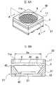
도 11은 제 1 종래예에 따른 LED램프의 단면도.11 is a sectional view of an LED lamp according to a first conventional example.
도 12는 제 2 종래예에 따른 LED램프의 단면도.12 is a sectional view of an LED lamp according to a second conventional example.
본 발명은 발광 다이오드(LED)에 관한 것이고, 보다 상세하게는 발광체에서 방출된 광의 포커싱, 발산 등을 위한 렌즈를 보호하도록 구성된 LED램프에 관한 것이다.BACKGROUND OF THE
LED램프는 이동 단말기, 가전, 조명, 차량, 자동 판매기 등에 널리 사용되고 있다. 종래의 LED램프(예컨대, 일본 특허 출원 공개 공보 제 2004-327955호, 0029절, 도 9 참조)의 제 1 예와 같은, 발광체에서 방출된 광이 렌즈를 통해 외부로 방출되는 LED램프가 잘 알려져 있다.LED lamps are widely used in mobile terminals, home appliances, lighting, vehicles, vending machines and the like. As the first example of a conventional LED lamp (e.g., Japanese Patent Application Laid-Open No. 2004-327955, Section 0029, see Fig. 9), an LED lamp in which light emitted from a light emitter is emitted to the outside through a lens is well known. have.
도 11은 종래의 LED램프의 제 1 예를 도시하고 있다. 도 11에 도시된 바와 같이, LED램프(71)는 전극 패턴이 형성된 회로 기판(22), 회로 기판(22)상에 장착되고 태이퍼링된 내주면을 갖는 오목부(32)를 포함하는 반사 프레임(31), 및 오목부(32)내의 중심부에 배치된 발광체(27)를 포함한다.11 shows a first example of a conventional LED lamp. As shown in FIG. 11, the
오목부(32)의 내주면상에 니켈 도금이나 기타 은색계통 도금으로 제조된 반사면(33)이 형성되어 발광체(27)에서 방출된 광이 상향으로 효과적으로 반사될 수 있다. 반사 프레임(31)상에는 투광성 밀봉판(74)가 배치되고 발광체(27)와 투광성 밀봉판(74)사이에는 공기층이 제공된다. 투광성 밀봉판(74)상에는 조화면을 포함하는 렌즈부(76)가 제공된다. 조화면 대신 마이크로렌즈, 프레넬 렌즈등이 사용될 수 있다.A
상기 구조에 의해, 발광체(27)에서 상향으로 방출되고 반사면(33)에 의해 반 사된 광이 렌즈부(76)에 의해 포커싱되어 발광체(27)로부터 외부로 방출된 광량을 증가시킨다.With this structure, the light emitted upward from the
더욱이, 종래의 LED램프(예컨대, 일본 특허 공개 공보 제 2003-158301호, 3페이지, 도 1참조)의 제 2 예와 같은, 회로 기판와 반사 프레임이 일체로 형성된 표면 장착 LED램프가 잘 알려져 있다.Moreover, surface-mounted LED lamps in which a circuit board and a reflection frame are integrally formed, such as the second example of a conventional LED lamp (for example, Japanese Patent Laid-Open No. 2003-158301,
도 12는 종래의 LED램프의 제 2 예인, 표면 장착 LED램프를 도시한 것이다.12 shows a surface mounted LED lamp, which is a second example of a conventional LED lamp.
도 12에 도시된 바와 같이, LED램프(1)는 도전 패턴(5)을 갖는 회로 기판(2) 및 회로 기판(2)상에 장착된 발광체로서 LED소자(10)를 포함한다. 회로 기판(2)에는 투광성 밀봉판(3)이 부착된다. 회로 기판(2)은 수지 몰딩 아티클상에 도전 회로와 전극을 형성하는 3차원 형상 회로 컴포넌트인 MID(사출성형 프린트 회로부품)로서 형성된다. LED엘리먼트(10)는 패키지에 제공된 오목부의 바닥면상에 장착된다. 두개의 LED엘리먼트(10)의 전극은 플립칩 본딩에 의해 범프(7)를 통해 회로 기판(2)의 도전 패턴(5)상에 장착된다.As shown in FIG. 12, the
투광성 밀봉판(3)은, 투광성 유리, 투광성 수지등과 같은 투광성 재료로 만들어지고, 시트형상이나 평판 형상을 가지며, 프레넬 렌즈, 마이크로 렌즈등과 같은 렌즈부(8)를 포함한다. LED엘리먼트(10)는 투광성을 확보하고 외부로의 광의 높은 포커싱을 달성하기 위해 투광성 밀봉판(3)으로 보호된다.The light-
그러나, 상기한 종래의 LED램프에는, 투광성 밀봉판의 렌즈부가 LED램프외부에 노출되어 있어서, 외부와의 접촉으로 인한 기계적 충격으로 렌즈부가 쉽게 파손된다. 렌즈부가 파손되면, LED램프를 사용할 수 없거나 렌즈에서 방출된 광의 광 학 특성의 열화와 같은 문제가 발생한다.However, in the conventional LED lamp described above, the lens portion of the translucent sealing plate is exposed to the outside of the LED lamp, so that the lens portion is easily damaged by mechanical shock due to contact with the outside. If the lens unit is broken, problems such as the inability of the LED lamp or the deterioration of the optical characteristics of the light emitted from the lens occur.
본 발명의 목적은 투광성 밀봉판의 렌즈부를 보호하고, 렌즈부에서 방출된 광의 고 광학 특성, 우수한 광휘도 특성, 및 LED램프의 장기적인 신뢰성을 얻을 수 있는 LED램프를 제공하는 데 있다.SUMMARY OF THE INVENTION An object of the present invention is to provide an LED lamp which protects the lens portion of the light-transmissive sealing plate and obtains high optical characteristics of light emitted from the lens portion, excellent brightness characteristics, and long-term reliability of the LED lamp.
이 목적을 달성하기 위해, 본 발명의 1실시예에 따른, LED램프는 전극 패턴을 포함하는 회로 기판, 회로 기판상에 제공된 발광체, 회로 기판상에 배치되고, 발광체를 둘러싸도록 형성된 반사면을 갖는 반사 프레임, 반사 프레임의 상면상에 제공되고, 발광체위에서, 렌즈부를 포함하는 투광성 밀봉판, 및 투광성 밀봉판의 방출 영역의 주변상에 배치되고 투광성 밀봉판의 렌즈부를 보호하도록 구성된 보호 부재를 포함한다.In order to achieve this object, an LED lamp according to an embodiment of the present invention has a circuit board including an electrode pattern, a light emitting body provided on the circuit board, a reflecting surface disposed on the circuit board and formed to surround the light emitting body. A reflective frame, provided on an upper surface of the reflective frame, on the light emitter, a transmissive sealing plate comprising a lens portion, and a protective member disposed on the periphery of the emission area of the translucent sealing plate and configured to protect the lens portion of the translucent sealing plate; .
따라서, 투광성 밀봉판, 특히 상기 투광성 밀봉판상에 있는 렌즈부는 보호 부재에 의해 효과적으로 보호된다.Thus, the transparent sealing plate, in particular the lens portion on the transparent sealing plate, is effectively protected by the protective member.
(바람직한 실시예의 상세한 설명)(Detailed Description of the Preferred Embodiments)
이후, 첨부한 도면을 참조하여 본 발명의 몇몇 바람직한 실시예를 상세하 설명할 것이다.Hereinafter, some preferred embodiments of the present invention will be described in detail with reference to the accompanying drawings.
[제 1 실시예][First Embodiment]
도 1은 본 발명의 제 1 실시예에 따른 LED램프(20)를 도시하고 있다. LED램프(20)는 회로 기판(2)과 그 회로 기판(2)상에 장착된 발광체(10)를 포함한다. 본 실시예의 회로 기판(2)은, 보드와 (도시안된) 그 보드상에 있는 도전 회로와 전극 이 일체로 형성되는 3차원형 회로 컴포넌트(성형 상호접속 장치)와 같은 방법으로 형성된다.1 shows an
이후, 회로 기판은 MID보드로 칭한다.The circuit board is hereinafter referred to as MID board.
발광체(10)는 본 실시예에서 적어도 하나의 LED소자를 포함한다.The
MID보드(2)는 오목부(4)를 갖고, 적당한 연결 메커니즘을 통해 오목부(4) 바닥면상에 LED소자(10)가 배치되어 회로 기판상에 있는 전극과 연결되고 있다.The
LED소자(10)를 덮고있는 투광성 밀봉판(3)이 MID보드(2) 상면에 배치되어 있는데, 투광성 밀봉판(3)은 LED소자(10)에서 외부로 광을 방출하기 위한 방출 영역(3a)을 구비한다. 방출 영역(3a)상에는 프레넬 렌즈나 마이크로렌즈등과 같은 렌즈부(8)가 구비되어 있다.A
투광성 밀봉판(3)의 소정 방출 영역주변에는 방출 영역에서 방출된 광을 차단시키지 않고 투광성 밀봉판(3)을 보호하는 보호 부재(11)가 배치되어 있다. 보호 부재(11)는 투광성 밀봉판(3)에 부착되어 본 실시예의 투광성 밀봉판(3)의 렌즈부(8)를 보호한다. 예컨대, 보호 부재(11)는 보호 부재를 통과하는 개구부(11a)를 구비하고 있다. 개구부(11a)의 내경은 대체로 렌즈부(8)의 렌즈 유효 직경(8a)과 같거나 크게 되어있다(도 1참조).The
따라서, 보호 부재(11)의 개구부(11a) 내부 모서리는 렌즈부(8)의 렌즈 유효 직경(8a)의 외주부에서 또는 렌즈 유효 직경(8a)의 외부에 놓이도록 배치되어 있다.Accordingly, the inner edge of the opening 11a of the
상기한 바와 같이, 본 실시예의 LED램프(20)에서는, 투광성 밀봉판(3)의 렌 즈부(8)가 보호 부재(11)로 보호되므로, 외부 충격에 의해 투광성 밀봉판(3)의 렌즈부(8)에 생기는 스크래치등을 방지할 수 있고, 렌즈부(8)의 광학 특성의 열화를 방지할 수 있다.As described above, in the
결과적으로, 개선된 휘도 특성과 장기적인 신뢰성을 갖는 LED램프(20)를 얻을 수 있다.As a result, the
보호 부재(11) 대신, 도 2에 도시된 바와 같은 보호 부재(12)를 사용할 수 있고, 보호 부재(12)는 개구부(12a)의 내경은 투광성 밀봉판(3)의 렌즈부(8)의 렌즈 유효 직경(8a)보다 상당히 크게 되어 있고, 개구부(12a) 내부 모서리는 렌즈부(8)의 렌즈 유효 직경(8a) 외부에 위치할 수 있고 보호 부재의 외경은 투광성 밀봉판(3)의 외주를 따라 배치될 수 있다.Instead of the
본 실시예에서도, 제 1 실시예와 같은 유리한 효과를 얻을 수 있다. 마찬가지로, 투광성 밀봉판(3)과 보호 부재(12)가 일체로 형성되는 구조에 의해 같은 효과를 얻을 수 있다.Also in this embodiment, the same advantageous effects as in the first embodiment can be obtained. Similarly, the same effect can be obtained by the structure in which the
[제 2 실시예]Second Embodiment
본 발명의 제 2 실시예에 따른 LED램프의 보호 부재는 제 1 실시예의 보호 부재와 다르지만, 기타 태양은 제 1 실시예의 LED램프와 마찬가지다. 따라서, 제 1 실시예와 일치하는 부분에는 같은 부재번호가 붙어있고, 그 설명은 생략한다.The protection member of the LED lamp according to the second embodiment of the present invention is different from the protection member of the first embodiment, but other aspects are the same as the LED lamp of the first embodiment. Therefore, parts corresponding to those in the first embodiment are assigned the same member numbers, and their description is omitted.
이하, 도 3을 참조하여, 제 2 실시예에 따른 LED램프를 설명한다.Hereinafter, the LED lamp according to the second embodiment will be described with reference to FIG. 3.
도 3에 도시된 바와 같이, 제 2 실시예의 LED램프(20) 보호 부재(13)의 개구부(13a) 내경은 투광성 밀봉판(3)에 인접한 1면에서, 그 1면과 대향하고 있는 보호 부재의 타면으로 점차 커지도록 되어 있다. 즉, 보호 부재(13)의 개구부(13a)는 투광성 밀봉판(3)에 인접한 소 직경(13b)과 투광성 밀봉판(3)에서 벗어나 있는 대 직경(13c)을 갖는다. 개구부(13a)는 대략 원추대형으로 되어 있고, 소 직경(13b) 위치에서 투광성 밀봉판(3)과 일체로 결합되어 있는 내면을 포함한다.As shown in Fig. 3, the inner diameter of the
개구부(13a)내 보호 부재(13)의 대략 원추대형 내면 전체 영역상에는 광반사층(14)이 형성된다. 개구부(13a)내 보호 부재(13)의 내면상에 있는 광반사층(14)은, 예컨대 금속막의 도금 또는 진공 증착으로 표면 처리된다.The
본 실시예에서 개구부(13a)내 보호 부재(13)의 내면이 대략 원추대형을 갖는 것으로 설명했지만, 본 실시예에서 이 형태로만 제한되지는 않고, 내주면을 각뿔대형, 또는 구면의 일부, 포물면의 일부, 비구면등과 같은 곡면으로 형성할 수도 있다.In the present embodiment, the inner surface of the
상기한 바와 같이, 본 실시예의 LED램프는, 보호 부재(13)의 개구부(13a)의 내경이 반사층(14)에 인접한 보호 부재의 1면에서 그 1면에 대향하는 보호 부재의 타면으로 점차 커지도록 되어 있고, 개구부(13a)내 보호 부재(13)의 내면이 대체로 대략 원추대형을 가지고 있고, 개구부(13a)내 보호 부재의 대략 원추대형 내면상에 형성된 광반사층(14)이 형성되므로, 개구부(13a)에서 방출된 광은 포커싱하여 빔이 된다.As described above, in the LED lamp of the present embodiment, the inner diameter of the
결과적으로, 렌즈부(8)에서 방출된 광은 반사되고 반사층(14)의 포커싱 특성은 증가한다. 제 1 실시예와 마찬가지의 방식으로 우수한 휘도 특성과 장기적인 신뢰성을 갖는 LED램프(20)를 얻을 수 있다.As a result, the light emitted from the
[제 3 실시예]Third Embodiment
본 발명의 제 3 실시예에 따른 LED램프는 보호 부재(13)의 상면상에 투광성 보호판이 구비되어 있지만, 기타 태양에서는 제 2 실시예의 LED램프와 같은 구조를 갖는다. 따라서, 제 2 실시예와 일치하는 부분에는 같은 부재 번호를 붙이고, 설명은 생략한다.The LED lamp according to the third embodiment of the present invention is provided with a transparent protective plate on the upper surface of the
이하, 도 4를 참조하여, 제 3 실시예에 따른 LED램프를 설명한다.Hereinafter, an LED lamp according to a third embodiment will be described with reference to FIG. 4.
도 4에 도시된 바와 같이, 제 3 실시예에 따른 LED램프(20)는 보호 부재(13)의 상면상에 구비되어 있는 투광성 보호판(15)을 포함한다. 투광성 보호판(15)은 시트형이나 납작한 판형의 아크릴, 폴리카보네이트등의 투광성 수지재 또는 유리재로 제조되고, 보호 부재(13)의 상면과 일체로 형성된다.As shown in FIG. 4, the
한편, 쉽게 스크래치가 생기지 않고 높은 광 투과성을 갖는 유리재를 사용하는 것이 바람직하다.On the other hand, it is preferable to use the glass material which does not produce a scratch easily and has high light transmittance.
상기한 바와 같이, 본 실시예에 따른, LED램프(20)는, 보호 부재(13)의 상면상에 투광성 보호판(15)이 구비되어 있으므로, 투광성 밀봉판(3)의 렌즈부(8)에 먼지가 부착하는 것을 방지하고 렌즈부(8)의 광학 특성이 열화하는 것을 방지할 수 있다. 더욱이, 내후성을 강화하기 위해 보호 부재(13)내에 자외선 차단 물질을 포함할 수 있다. 더욱이, 제 2 실시예에서와 같은 방식으로, 포커싱 특성이 강화된 고반사광이 렌즈부에서 방출될 수 있다. 따라서, 우수한 휘도 특성과 장기적인 신뢰성을 갖는 LED램프를 얻을 수 있다.As described above, the
본 실시예에서, 보호 부재(13)의 상면상에 투광성 보호판(15)이 구비되어 있 는 예에 대해 설명했지만, 제 1 실시예의 보호 부재(11 또는 12)상에 투광성 보호판(15)이 구비되어 있어도 마찬가지의 유리한 효과를 얻을 수 있다.In the present embodiment, an example in which the transmissive
한편, 각각의 실시예에서 투광성 밀봉판(3)의 렌즈부(8)가 투광성 보호판(15) 면과 마주하도록 배치되어 있지만, 도 5에 도시된 바와 같이, 렌즈부(8)가 LED소자(10)와 마주하도록 배치되어 있더라도 동일한 효과를 얻을 수 있다.On the other hand, in each embodiment, the
[제 4 실시예][Example 4]
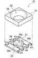
도 6A 및 6B에서는 본 발명의 제 4 실시예에 따른 LED램프에 대해서 설명한다.6A and 6B illustrate an LED lamp according to a fourth embodiment of the present invention.
도 6A 및 6B에 도시된 바와 같이, 본 실시예의 LED램프(20)는 LED램프의 본체부(21)와 그 본체부(21)의 상면상에 구비되어 있고 렌즈부(8)를 갖는 투광성 밀봉판(3)을 포함한다. 투광성 밀봉판(3)의 방출 영역이 있는 표면상에는 제 1 실시예의 보호 부재와 같은 보호 부재(11)가 배치된다.As shown in Figs. 6A and 6B, the
도 7 내지 도 10에 도시된 바와 같이, LED램프의 본체부(21)는 3조의 애노드 및 캐소드 전극이 형성되어 있는 회로 기판(22), 그 회로 기판상에 장착된 발광체(27), 및 발광체(27)를 둘러싸도록 구성된 반사면(33)을 포함하는 반사 프레임(31)을 포함한다.As shown in Figs. 7 to 10, the
도 9에 도시된 바와 같이, 회로 기판(22)은 사각형의 유리 에폭시나 BT수지등으로 제조된다. 애노드 전극(A1, A2, 및 A3)과 캐소드 전극(K1, K2, 및 K3)은 회로 기판(22)의 대향측에 배치되고 쓰루홀로 형성된다. 애노드 전극(A1, A2, 및 A3)과 캐소드 전극(K1, K2, 및 K3)의 리드 패턴은 회로 기판(22)의 1측에서 중심부 로 뻗어있도록 형성되어 있다. 회로 기판(22)상에는 3개의 LED소자(28a, 28b, 28c)가 장착된다. 보다 상세하게는, LED소자(28a)는 리드 패턴A1과 K1사이에, LED소자(28b)는 리드 패턴A2와 K2사이에, 그리고 LED소자(28c)는 리드 패턴A3와 K3사이에서 와이어본딩으로 연결된다.As shown in Fig. 9, the
본 실시예에서, 발광체(27)는 3개의 LED소자(28a, 28b, 28c)와 이 3개의 LED소자를 밀봉하기 위한 투명 내지 투광성 수지재(29)를 포함한다. 도 9에 도시된 바와 같이, LED소자(28a, 28b, 28c)는 질화 갈륨계 화합물의 반도체로 형성되고 회로 기판(22)의 중심부에서 삼각형으로 균등하게 형성된다.In this embodiment, the
도 7 및 8에 도시된 바와 같이, 반사 프레임(31)은 일반적으로 회로 기판(22)과 같이 평면형의 컴포넌트로서 회로 기판(22)상에 배치된다. 또한, 반사 프레임(31)의 두께는 회로 기판(22) 보다 크고 반사 프레임의 중심부에 형성되어 발광체(27)를 둘러싸도록 배치되어 있는 원추형 오목부(32)를 포함한다. 오목부(32)는 발광체(27)에서 방출된 광을 균등하게 포커싱하기 위한 원형의 내주면과, 위로 갈수록 넓어지는 테이퍼를 갖는다.As shown in FIGS. 7 and 8, the
발광체(27)에서 방출된 광은, 오목부(32)의 내주면상에 니켈 도금이나 기타 은색계통 도금을 한 반사면(33)을 형성하여 상향으로 효과적으로 반사시킬 수 있다. 반사면(33)의 모양과 경사각은 LED램프의 본체부(21)의 제원에 따라 적절하게 정할 것이지만, 카메라 플래시 광원으로 LED램프를 사용할때 특정 거리로 위치된 대상을 균등하게 조명하기 위해, 발광체(27)에 중심을 맞추고 40 내지 80도 범위로 상향으로 기울어진 반구형 반사면이 바람직하다.The light emitted from the
도 10에 도시된 바와 같이, 본체부(21)는, 애노드 전극(A1, A2, 및 A3)과 캐소드 전극(K1, K2, 및 K3)이 구비되어 있는 회로 기판(22)상에 LED소자(28a 내지 28c)를 장착하고, 수지재(29)로 LED소자를 밀봉한후, 회로 기판(22)에 반사 프레임(31)을 부가하여 형성된다.As shown in FIG. 10, the
상기 본체부(21)에서는, 3개의 LED소자(28a, 28b, 28c)를 포함하는 발광체(27)에서 직접적으로 상향으로 방출된 광과, 반사면(33)에서 반사된 광의 조합에 의해 발광체(27)에서 전방으로 방출된 광의 휘도가 크게 증가할 수 있다.In the
더욱이, 도 8에 도시된 바와 같이, 반사면(33)에 의해 진행 방향으로 광을 포커싱함으로써 발광체(27)에서 방출된 광을 소정 방향으로 진행하게 할 수 있고, 반사 프레임(31)의 윤곽은 일반적으로 회로 기판(22)의 윤곽과 평면에서 같은 크기를 가지고 있고 반사 프레임과 회로 기판의 외주면상에 돌출부가 없기 때문에 좁은 공간에서 LED램프를 장착할 수 있다.Furthermore, as shown in FIG. 8, by focusing the light in the advancing direction by the reflecting
따라서, 카메라 기능이 있는 휴대폰이나 기타 장치에 쉽게 LED램프를 장착할 수 있고 플래시의 광원으로 LED램프를 사용할때 충분한 광량을 얻을 수 있다. 발광체(27)에 포함된 각각의 LED소자는 개별 전극쌍(A1 및 K1, A2 및 K2, A3 및 K3)을 가지고 있기 때문에, LED소자(28a, 28b, 28c)중 어느 하나, 둘, 또는 3개 전부를 조명시킬 수 있다.Therefore, the LED lamp can be easily mounted on a mobile phone or other device having a camera function, and sufficient light quantity can be obtained when using the LED lamp as a light source of the flash. Since each LED element included in the light-emitting
한편, 본 실시예에서, 발광체(27)가 3개의 LED소자(28a, 28b, 28c)를 포함하지만, LED의 수는 제한되지 않으므로, 필요한 분야에 따라 1개, 2개 또는 4개 이상의 LED소자를 사용할 수도 있다.On the other hand, in the present embodiment, the
본 실시예의 LED램프(30)는 렌즈부(8)를 구비하고, 공기층(40)을 포함하도록 하는 반사 프레임(31)상에 배치되어 있는 투광성 밀봉판(3)과 투광성 밀봉판(3)에 의해 폐쇄된 오목부(32)내에 있는 발광체(27)를 제공하고 방출 영역을 차단시키지 않으면서 방출 영역주위의 투광성 밀봉판(3)상에 보호 부재(11)를 배치하여 형성된다.The
상기한 바와 같이 보호 부재(11)는 투광성 밀봉판(3)의 렌즈부(8)를 보호하기 위해 제공되는 것이고 보호 부재의 두께 방향으로 뻗어있는 축을 갖는 개구부(11a)를 포함하는데, 개구부(11a)의 내경은 일반적으로 렌즈부(8)의 렌즈 유효 직경(8a)과 같게 되어 있고 개구부(11a) 내부의 모서리는 렌즈 유효 직경(8a)의 외주에 놓이도록 배치된다.As described above, the
투광성 밀봉판(3)은, 예컨대 방출 영역상에 형성된 마이크로 렌즈를 포함하는 렌즈부(8)를 구비하고 있고, 투명 또는 투광성 수지재를 형성하거나 소정의 형상으로 유리재를 직접 성형함으로써 제조된다. 투광성 밀봉판(3)과 보호 부재(11)는 일체로 형성할 수 있다.The
공기층(40)은 투광성 밀봉판(3) 아래 구비되어 있기 때문에, 발광체(27)에서 방출된 광은, 외부로 방출되기 전에, 서로 다른 굴절률을 갖는 공기층(40)과 투광성 밀봉판(3)의 2개의 매체를 통과한다. 굴절률을 변경하여 높은 광 포커싱 효과를 얻을 수 있다.Since the
본 실시예의 LED램프(30)에서는, 투광성 밀봉판(3)이 반사 프레임(31)상에 구비되어 있기 때문에, 오목부가 폐쇄된 상태로 있다. 따라서 오목부(32)내의 공 기층(40)이 팽창할 수 있다는 문제가 있다. 이 점을 개선하기 위해, 공기층(40)과 외부간 연통가능하도록 공기 구멍(45)을 두어 오목부의 압력을 감소시킨다. 따라서, 안전하고도 견고하게 리플로우 처리를 수행하여 LED램프의 품질 열화를 줄일 수 있다.In the
상기한 바와 같이, 본 실시예의 LED램프(30)에서는, 투광성 밀봉판(3)의 렌즈부(8)가 외부 충격에서 보호되어 렌즈부(8)의 파손이나 광학 특성의 열화를 방지할 수 있다. 결과적으로, 우수한 휘도 특성과 장기적인 신뢰성을 갖는 LED램프를 얻을 수 있다.As described above, in the
한편, 본 실시예에서, 렌즈부(8)가 마이크로 렌즈인 경우에 대해 설명했지만, 이로써 제한되지 않고, 프레넬 렌즈나 조화면으로써도 마찬가지의 효과를 얻을 수 있다.On the other hand, although the case where the
또한, LED램프를 백색 발광시켜 플래시의 광원과 같은 예에서 사용하기 위한 구성에는 두 가지가 있다.In addition, there are two types of configurations for use in an example such as a light source of a flash by emitting white LED lamps.
제 1 구성은 도 9에 도시된 것과 같이 발광체(27)에 청색 발광형 LED소자(28a, 28b, 28c)를 사용하는 구성이고, LED소자를 밀봉하는 수지에, 예컨대 YAG형광물질을 혼입한다.As shown in Fig. 9, the first configuration uses the blue light emitting
제 2 구성은 발광체(27)에서 적녹청색 발광형 LED소자를 사용하는 구성이고, 이 3가지 LED소자에서 방출되는 광의 색깔이나 휘도를 조절하여 백색광 방출을 얻을 수 있다.The second configuration is a configuration in which the red light blue LED device is used in the
제 1 구성에서는, 형광 물질 및/또는 착색제와 적어도 하나의 LED소자를 결 합하여 원하는 광 방출 색을 얻을 수 있다. 제 2 구성에서는, 다양한 광 방출 색을 만들 수 있고 백색광 방출에 제한되지 않는다.In the first configuration, the fluorescent material and / or the colorant and the at least one LED element can be combined to obtain a desired light emission color. In the second configuration, various light emission colors can be made and are not limited to white light emission.
더욱이, 보호 부재(11) 대신 제 1 및 제 2 실시예의 보호 부재(12 또는 13)를 사용하여, 렌즈부에서 방출된 광의 반사율과 광의 광학 특성을 증가시킬 수 있다.Moreover, the
더욱이, 보호 부재(11, 12, 또는 13)상에 제 3 실시예의 투광성 보호판(15)을 제공하여, 투광성 밀봉판(3)의 렌즈부(8)에 먼지가 부착되는 것을 막아서, 렌즈부(8)의 광학 특성의 열화를 방지할 수 있다.Furthermore, the transparent
더욱이, 투광성 밀봉판(3)의 렌즈부(8)가 발광체(27)와 마주하는 면상에 구비되는 것으로 되어 있지만, 다른 실시예에서도 마찬가지의 효과를 얻을 수 있다.Moreover, although the
또한, 상기 실시예의 LED램프가 가시광선을 방출하지만, 적외선이나 자외선을 방출할 수도 있다.In addition, although the LED lamp of the above embodiment emits visible light, it may emit infrared rays or ultraviolet rays.
본 발명의 바람직한 실시예에 대하여 설명했지만, 본 발명은 본 실시예에만 제하되지는 않고 바람직한 실시예에 대한 다양한 변경과 변화를 가할 수 있다.Although the preferred embodiment of the present invention has been described, the present invention is not limited only to the present embodiment, but various modifications and changes can be made to the preferred embodiment.
상기한 바와 같이 본 발명에 의하여 투광성 밀봉판의 렌즈부를 보호하고, 렌즈부에서 방출된 광의 고 광학 특성, 우수한 광휘도 특성, 및 LED램프의 장기적인 신뢰성을 얻을 수 있는 LED램프를 제공할 수 있다.According to the present invention as described above, it is possible to provide an LED lamp that protects the lens portion of the light-transmissive sealing plate and obtains high optical characteristics, excellent light brightness characteristics, and long-term reliability of the LED lamps emitted from the lens portion.
Claims (22)
Translated fromKoreanApplications Claiming Priority (2)
| Application Number | Priority Date | Filing Date | Title |
|---|---|---|---|
| JP2004230104AJP2006049657A (en) | 2004-08-06 | 2004-08-06 | LED lamp |
| JPJP-P-2004-00230104 | 2004-08-06 |
Publications (1)
| Publication Number | Publication Date |
|---|---|
| KR20060049072Atrue KR20060049072A (en) | 2006-05-18 |
Family
ID=35756572
Family Applications (1)
| Application Number | Title | Priority Date | Filing Date |
|---|---|---|---|
| KR1020050071039AWithdrawnKR20060049072A (en) | 2004-08-06 | 2005-08-03 | LED lamp |
Country Status (6)
| Country | Link |
|---|---|
| US (1) | US20060027828A1 (en) |
| JP (1) | JP2006049657A (en) |
| KR (1) | KR20060049072A (en) |
| CN (1) | CN1731593A (en) |
| DE (1) | DE102005036742A1 (en) |
| TW (1) | TW200625682A (en) |
Cited By (5)
| Publication number | Priority date | Publication date | Assignee | Title |
|---|---|---|---|---|
| KR101146097B1 (en)* | 2011-02-21 | 2012-05-16 | 주식회사 루멘스 | Light emitting device package and backlight module comprising the same |
| US8613533B2 (en) | 2010-07-28 | 2013-12-24 | Lg Innotek Co., Ltd. | Optical sheet and light emitting device package having the same |
| KR20150111105A (en)* | 2014-03-25 | 2015-10-05 | 엘지이노텍 주식회사 | Light emitting device package |
| US9632355B2 (en) | 2014-10-10 | 2017-04-25 | Samsung Display Co., Ltd. | Display device |
| WO2020040401A1 (en)* | 2018-08-24 | 2020-02-27 | 주식회사 케이티앤지 | Light-emitting element and aerosol generation device comprising same |
Families Citing this family (57)
| Publication number | Priority date | Publication date | Assignee | Title |
|---|---|---|---|---|
| US7365026B2 (en)* | 2005-02-01 | 2008-04-29 | Taiwan Semiconductor Manufacturing Company, Ltd. | CxHy sacrificial layer for cu/low-k interconnects |
| US7726844B2 (en) | 2005-03-31 | 2010-06-01 | Neobulb Technologies, Inc. | Illuminating equipment using high power LED with high efficiency of heat dissipation |
| JP2007300069A (en)* | 2006-04-04 | 2007-11-15 | Toyoda Gosei Co Ltd | LIGHT EMITTING ELEMENT, LIGHT EMITTING DEVICE USING THE LIGHT EMITTING ELEMENT, AND METHOD FOR PRODUCING THE LIGHT EMITTING ELEMENT |
| JP4628302B2 (en)* | 2006-04-24 | 2011-02-09 | 株式会社エンプラス | Lighting device and lens of lighting device |
| US7888868B2 (en)* | 2006-04-28 | 2011-02-15 | Avago Technologies General Ip (Singapore) Pte. Ltd. | LED light source with light-directing structures |
| JP5041732B2 (en)* | 2006-05-16 | 2012-10-03 | アルプス電気株式会社 | Luminescent body and manufacturing method thereof |
| US7839072B2 (en) | 2006-05-24 | 2010-11-23 | Citizen Electronics Co., Ltd. | Translucent laminate sheet and light-emitting device using the translucent laminate sheet |
| KR100813066B1 (en) | 2006-06-30 | 2008-03-14 | 엘지전자 주식회사 | Lens substrate, light emitting device package and backlight unit using same |
| USD566055S1 (en)* | 2006-09-21 | 2008-04-08 | Lg Innotek Co., Ltd. | Light-emitting diode (LED) |
| TWI313943B (en)* | 2006-10-24 | 2009-08-21 | Chipmos Technologies Inc | Light emitting chip package and manufacturing thereof |
| US7737636B2 (en)* | 2006-11-09 | 2010-06-15 | Intematix Corporation | LED assembly with an LED and adjacent lens and method of making same |
| EP1925874B8 (en) | 2006-11-24 | 2014-09-10 | OSRAM GmbH | LED color-mixing lighting system |
| US8330176B2 (en) | 2007-02-13 | 2012-12-11 | 3M Innovative Properties Company | LED devices having lenses and methods of making same |
| US9944031B2 (en)* | 2007-02-13 | 2018-04-17 | 3M Innovative Properties Company | Molded optical articles and methods of making same |
| JP2008305642A (en)* | 2007-06-06 | 2008-12-18 | Sony Corp | Light-emitting device, surface light source, and image display device |
| CN101720407A (en)* | 2007-06-25 | 2010-06-02 | 陈振贤 | Light emitting diode lighting device |
| WO2009000106A1 (en)* | 2007-06-25 | 2008-12-31 | Jenshyan Chen | Led lighting device |
| DE102007057671A1 (en)* | 2007-11-30 | 2009-06-04 | Osram Opto Semiconductors Gmbh | lighting device |
| JP5418762B2 (en) | 2008-04-25 | 2014-02-19 | ソニー株式会社 | Light emitting device and display device |
| TWI384651B (en)* | 2008-08-20 | 2013-02-01 | Au Optronics Corp | Light-emitting diode structure and manufacturing method thereof |
| WO2010053193A1 (en)* | 2008-11-10 | 2010-05-14 | シャープ株式会社 | Light-emitting device, surface light source, and display device |
| US20100123386A1 (en) | 2008-11-13 | 2010-05-20 | Maven Optronics Corp. | Phosphor-Coated Light Extraction Structures for Phosphor-Converted Light Emitting Devices |
| JP2010171342A (en) | 2009-01-26 | 2010-08-05 | Sony Corp | Color conversion member, method of manufacturing the same, light-emitting device, and display |
| JP5428358B2 (en)* | 2009-01-30 | 2014-02-26 | ソニー株式会社 | Method for manufacturing optical element package |
| JP2010225373A (en) | 2009-03-23 | 2010-10-07 | Sony Corp | Color conversion sheet, illumination device, and display device |
| JP2010251686A (en)* | 2009-03-26 | 2010-11-04 | Harison Toshiba Lighting Corp | Light emitting device and manufacturing method thereof |
| US8033691B2 (en) | 2009-05-12 | 2011-10-11 | Koninklijke Philips Electronics N.V. | LED lamp producing sparkle |
| KR101421963B1 (en)* | 2010-01-25 | 2014-07-24 | 삼성전자주식회사 | LIGHT EMITTING DIODE FLASH MODULE OF CAMERA and CAMERA APPARATAUS |
| KR101045034B1 (en) | 2010-02-25 | 2011-06-30 | 인하대학교 산학협력단 | White LED with multi-layered micro lens |
| CN102192417A (en)* | 2010-03-01 | 2011-09-21 | 亿光电子工业股份有限公司 | Light source module and lamp |
| CN102980072A (en)* | 2010-03-01 | 2013-03-20 | 亿光电子工业股份有限公司 | Light source modules and lamps |
| US20110255276A1 (en)* | 2010-04-19 | 2011-10-20 | Coward Mark T | Lighting assembly |
| KR101082404B1 (en) | 2010-05-10 | 2011-11-10 | 신화에코필 주식회사 | Optical lens and optical package having same |
| EP2458268B1 (en)* | 2010-11-26 | 2016-04-20 | LG Innotek Co., Ltd. | Phosphor plate and lighting device |
| CN102593308A (en)* | 2011-01-11 | 2012-07-18 | 展晶科技(深圳)有限公司 | Light emitting diode package structure |
| TWI517452B (en)* | 2011-03-02 | 2016-01-11 | 建準電機工業股份有限公司 | Polycrystalline package structure of luminescent crystal |
| WO2013007206A1 (en)* | 2011-07-12 | 2013-01-17 | 东莞巨扬电器有限公司 | Condenser lens applicable in led lighting apparatus |
| KR101849126B1 (en) | 2011-08-29 | 2018-04-16 | 엘지이노텍 주식회사 | Light Emitting Device Package |
| KR101959035B1 (en) | 2011-10-31 | 2019-03-18 | 서울바이오시스 주식회사 | Light emitting diode package and method of fabricating the same |
| JP6338533B2 (en)* | 2011-12-22 | 2018-06-06 | ヘプタゴン・マイクロ・オプティクス・プライベート・リミテッドHeptagon Micro Optics Pte. Ltd. | Optoelectronic module, in particular flash module and method of manufacturing the same |
| CN103311418B (en)* | 2012-03-06 | 2017-05-24 | 展晶科技(深圳)有限公司 | Light emitting diode module |
| JPWO2014064871A1 (en)* | 2012-10-25 | 2016-09-08 | パナソニックIpマネジメント株式会社 | LIGHT EMITTING DEVICE, ITS MANUFACTURING METHOD, AND LIGHT EMITTING DEVICE PACKAGE |
| WO2014098768A1 (en)* | 2012-12-20 | 2014-06-26 | Heptagon Micro Optics Pte. Ltd. | Opto-electronic modules with masking feature for reducing the visibility of interior components |
| CN103579458A (en)* | 2013-10-23 | 2014-02-12 | 西安重装渭南光电科技有限公司 | LED packaging structure and method thereof |
| CN103579457A (en)* | 2013-10-23 | 2014-02-12 | 西安重装渭南光电科技有限公司 | LED integration packaging structure and method thereof |
| DE102014107960A1 (en)* | 2014-06-05 | 2015-12-17 | Osram Opto Semiconductors Gmbh | Optoelectronic component |
| WO2016014762A1 (en) | 2014-07-23 | 2016-01-28 | Crystal Is, Inc. | Photon extraction from ultraviolet light-emitting devices |
| JP6602622B2 (en)* | 2014-09-25 | 2019-11-06 | 山村フォトニクス株式会社 | Optical device apparatus and protective cover for covering optical device |
| KR20160038094A (en)* | 2014-09-26 | 2016-04-07 | 코닝정밀소재 주식회사 | Substrate for color conversion of led and method of fabricating threof |
| JP6572906B2 (en) | 2014-11-14 | 2019-09-11 | 凸版印刷株式会社 | Optical barrier film, color conversion film, and backlight unit |
| DE102015104220A1 (en)* | 2015-03-20 | 2016-09-22 | Osram Opto Semiconductors Gmbh | Optoelectronic lighting device |
| EP3279708A4 (en) | 2015-03-30 | 2018-08-15 | Toppan Printing Co., Ltd. | Optical film, method for manufacturing same, optical barrier film, and color conversion film |
| CN106200088A (en)* | 2015-05-07 | 2016-12-07 | 怡来汽车零部件系统株式会社 | the display cover unit of display device |
| JP2018060989A (en)* | 2016-10-04 | 2018-04-12 | 日本特殊陶業株式会社 | Frame member, light-emitting device, and manufacturing method thereof |
| JP7184599B2 (en) | 2018-11-06 | 2022-12-06 | ローム株式会社 | semiconductor light emitting device |
| CN116794879A (en)* | 2022-03-18 | 2023-09-22 | 海信视像科技股份有限公司 | Display device |
| US12320492B1 (en) | 2023-12-04 | 2025-06-03 | Leviton Manufacturing Co., Inc. | Lighting fixture systems |
Family Cites Families (27)
| Publication number | Priority date | Publication date | Assignee | Title |
|---|---|---|---|---|
| US3911430A (en)* | 1974-04-17 | 1975-10-07 | Fairchild Camera Instr Co | Alpha-numeric display package |
| JPS5991764U (en)* | 1982-12-10 | 1984-06-21 | ロ−ム株式会社 | light emitting diode lamp |
| JPS6338270A (en)* | 1986-08-04 | 1988-02-18 | Omron Tateisi Electronics Co | Light emitting and receiving device |
| JPH04109556U (en)* | 1991-03-08 | 1992-09-22 | シヤープ株式会社 | Reflective case type LED lamp |
| JPH06104480A (en)* | 1992-09-21 | 1994-04-15 | Nec Corp | Method for manufacturing semiconductor optical device |
| JP2740931B2 (en)* | 1992-12-29 | 1998-04-15 | 京セラ株式会社 | Image forming device |
| US5836676A (en)* | 1996-05-07 | 1998-11-17 | Koha Co., Ltd. | Light emitting display apparatus |
| US6517213B1 (en)* | 1997-03-31 | 2003-02-11 | Idec Izumi Corporation | Indicator device and illumination device |
| JP3378465B2 (en)* | 1997-05-16 | 2003-02-17 | 株式会社東芝 | Light emitting device |
| JP3253558B2 (en)* | 1997-05-19 | 2002-02-04 | 株式会社三協精機製作所 | Objective lens drive |
| JP3900606B2 (en)* | 1997-07-17 | 2007-04-04 | シチズン電子株式会社 | Infrared data communication module |
| JPH11163412A (en)* | 1997-11-25 | 1999-06-18 | Matsushita Electric Works Ltd | Led illuminator |
| JP4406490B2 (en)* | 2000-03-14 | 2010-01-27 | 株式会社朝日ラバー | Light emitting diode |
| WO2001091090A1 (en)* | 2000-05-26 | 2001-11-29 | Showers International Pty Ltd | Illumination of signs and system for providing signs |
| JP2001351997A (en)* | 2000-06-09 | 2001-12-21 | Canon Inc | Mounting structure of light receiving sensor and method of using the same |
| US6616299B2 (en)* | 2001-02-02 | 2003-09-09 | Gelcore Llc | Single optical element LED signal |
| JP4050482B2 (en)* | 2001-04-23 | 2008-02-20 | 豊田合成株式会社 | Semiconductor light emitting device |
| JP2003158301A (en)* | 2001-11-22 | 2003-05-30 | Citizen Electronics Co Ltd | Light emitting diode |
| US6924514B2 (en)* | 2002-02-19 | 2005-08-02 | Nichia Corporation | Light-emitting device and process for producing thereof |
| US6729744B2 (en)* | 2002-03-29 | 2004-05-04 | Pat Y. Mah | Faraday flashlight |
| DE10245580B4 (en)* | 2002-09-27 | 2006-06-01 | Siemens Ag | Device for generating an image |
| JP4504662B2 (en)* | 2003-04-09 | 2010-07-14 | シチズン電子株式会社 | LED lamp |
| US6903380B2 (en)* | 2003-04-11 | 2005-06-07 | Weldon Technologies, Inc. | High power light emitting diode |
| DE10318932A1 (en)* | 2003-04-26 | 2004-11-25 | Aqua Signal Aktiengesellschaft Spezialleuchtenfabrik | Lantern, preferably for use on board ships, in particular on pleasure boats |
| US6828590B2 (en)* | 2003-05-07 | 2004-12-07 | Bear Hsiung | Light emitting diode module device |
| CA2634475C (en)* | 2003-07-07 | 2014-05-20 | Brasscorp Limited | Led-based inspection lamp with improved collimation optics |
| US7183587B2 (en)* | 2003-09-09 | 2007-02-27 | Cree, Inc. | Solid metal block mounting substrates for semiconductor light emitting devices |
- 2004
- 2004-08-06JPJP2004230104Apatent/JP2006049657A/enactivePending
- 2005
- 2005-08-03KRKR1020050071039Apatent/KR20060049072A/ennot_activeWithdrawn
- 2005-08-03TWTW094126358Apatent/TW200625682A/enunknown
- 2005-08-04DEDE102005036742Apatent/DE102005036742A1/ennot_activeWithdrawn
- 2005-08-05CNCNA2005100894166Apatent/CN1731593A/enactivePending
- 2005-08-08USUS11/198,389patent/US20060027828A1/ennot_activeAbandoned
Cited By (7)
| Publication number | Priority date | Publication date | Assignee | Title |
|---|---|---|---|---|
| US8613533B2 (en) | 2010-07-28 | 2013-12-24 | Lg Innotek Co., Ltd. | Optical sheet and light emitting device package having the same |
| KR101146097B1 (en)* | 2011-02-21 | 2012-05-16 | 주식회사 루멘스 | Light emitting device package and backlight module comprising the same |
| KR20150111105A (en)* | 2014-03-25 | 2015-10-05 | 엘지이노텍 주식회사 | Light emitting device package |
| US9632355B2 (en) | 2014-10-10 | 2017-04-25 | Samsung Display Co., Ltd. | Display device |
| WO2020040401A1 (en)* | 2018-08-24 | 2020-02-27 | 주식회사 케이티앤지 | Light-emitting element and aerosol generation device comprising same |
| KR20200023060A (en)* | 2018-08-24 | 2020-03-04 | 주식회사 케이티앤지 | Light emitting element and Aerosol generating device including the same |
| US11304449B2 (en) | 2018-08-24 | 2022-04-19 | Kt&G Corporation | Light-emitting element and aerosol generation device comprising same |
Also Published As
| Publication number | Publication date |
|---|---|
| DE102005036742A1 (en) | 2006-06-01 |
| TW200625682A (en) | 2006-07-16 |
| JP2006049657A (en) | 2006-02-16 |
| CN1731593A (en) | 2006-02-08 |
| US20060027828A1 (en) | 2006-02-09 |
Similar Documents
| Publication | Publication Date | Title |
|---|---|---|
| KR20060049072A (en) | LED lamp | |
| JP5797393B2 (en) | Light emitting device package | |
| CN102130109B (en) | Light emitting device and light unit using the same | |
| JP7460936B2 (en) | light source device | |
| US8253154B2 (en) | Lens for light emitting diode package | |
| TWI750476B (en) | Light-emitting device and surface-emitting light source | |
| US20110149601A1 (en) | Light emitting device and light unit using the same | |
| KR20170135689A (en) | Light emitting device and method for manufacturing the same | |
| JP6703312B2 (en) | Light emitting module and surface emitting light source | |
| CN207338367U (en) | Light emitting diode and light emitting module | |
| KR20130104628A (en) | Led illumination module | |
| US10678036B2 (en) | Optical device and light source module including the same | |
| KR101655463B1 (en) | Light emitting device package and light unit having the same | |
| KR20140095913A (en) | Light emitting module and light apparatus having thereof | |
| KR102432222B1 (en) | Optical plate, lighting device, and lighting module | |
| KR20170052208A (en) | Optical plate, lighting device, and lighting module | |
| KR101997240B1 (en) | Lighting device | |
| KR101877410B1 (en) | Light-emitting device | |
| KR20200118733A (en) | Lighting module and lighting device | |
| KR101704035B1 (en) | Light emitting device package | |
| KR102432223B1 (en) | Lighting apparatus | |
| KR101704032B1 (en) | Light emitting device package and light emitting system | |
| KR102450123B1 (en) | Optical plate, lighting device, and lighting module | |
| KR102402259B1 (en) | A light emitting device package | |
| KR20170052199A (en) | Optical plate, lighting device, and lighting module |
Legal Events
| Date | Code | Title | Description |
|---|---|---|---|
| PA0109 | Patent application | Patent event code:PA01091R01D Comment text:Patent Application Patent event date:20050803 | |
| PG1501 | Laying open of application | ||
| PC1203 | Withdrawal of no request for examination | ||
| WITN | Application deemed withdrawn, e.g. because no request for examination was filed or no examination fee was paid |