KR20060027593A - LCD and its driving method - Google Patents
LCD and its driving methodDownload PDFInfo
- Publication number
- KR20060027593A KR20060027593AKR1020040076457AKR20040076457AKR20060027593AKR 20060027593 AKR20060027593 AKR 20060027593AKR 1020040076457 AKR1020040076457 AKR 1020040076457AKR 20040076457 AKR20040076457 AKR 20040076457AKR 20060027593 AKR20060027593 AKR 20060027593A
- Authority
- KR
- South Korea
- Prior art keywords
- gate
- signal
- odd
- pixels
- transistor
- Prior art date
- Legal status (The legal status is an assumption and is not a legal conclusion. Google has not performed a legal analysis and makes no representation as to the accuracy of the status listed.)
- Granted
Links
Images


Classifications
- G—PHYSICS
- G09—EDUCATION; CRYPTOGRAPHY; DISPLAY; ADVERTISING; SEALS
- G09G—ARRANGEMENTS OR CIRCUITS FOR CONTROL OF INDICATING DEVICES USING STATIC MEANS TO PRESENT VARIABLE INFORMATION
- G09G3/00—Control arrangements or circuits, of interest only in connection with visual indicators other than cathode-ray tubes
- G09G3/20—Control arrangements or circuits, of interest only in connection with visual indicators other than cathode-ray tubes for presentation of an assembly of a number of characters, e.g. a page, by composing the assembly by combination of individual elements arranged in a matrix no fixed position being assigned to or needed to be assigned to the individual characters or partial characters
- G09G3/34—Control arrangements or circuits, of interest only in connection with visual indicators other than cathode-ray tubes for presentation of an assembly of a number of characters, e.g. a page, by composing the assembly by combination of individual elements arranged in a matrix no fixed position being assigned to or needed to be assigned to the individual characters or partial characters by control of light from an independent source
- G09G3/36—Control arrangements or circuits, of interest only in connection with visual indicators other than cathode-ray tubes for presentation of an assembly of a number of characters, e.g. a page, by composing the assembly by combination of individual elements arranged in a matrix no fixed position being assigned to or needed to be assigned to the individual characters or partial characters by control of light from an independent source using liquid crystals
- G09G3/3611—Control of matrices with row and column drivers
- G09G3/3674—Details of drivers for scan electrodes
- G09G3/3677—Details of drivers for scan electrodes suitable for active matrices only
- G—PHYSICS
- G11—INFORMATION STORAGE
- G11C—STATIC STORES
- G11C19/00—Digital stores in which the information is moved stepwise, e.g. shift registers
- G11C19/18—Digital stores in which the information is moved stepwise, e.g. shift registers using capacitors as main elements of the stages
- G11C19/182—Digital stores in which the information is moved stepwise, e.g. shift registers using capacitors as main elements of the stages in combination with semiconductor elements, e.g. bipolar transistors, diodes
- G11C19/184—Digital stores in which the information is moved stepwise, e.g. shift registers using capacitors as main elements of the stages in combination with semiconductor elements, e.g. bipolar transistors, diodes with field-effect transistors, e.g. MOS-FET
- G—PHYSICS
- G11—INFORMATION STORAGE
- G11C—STATIC STORES
- G11C19/00—Digital stores in which the information is moved stepwise, e.g. shift registers
- G11C19/28—Digital stores in which the information is moved stepwise, e.g. shift registers using semiconductor elements
- G—PHYSICS
- G09—EDUCATION; CRYPTOGRAPHY; DISPLAY; ADVERTISING; SEALS
- G09G—ARRANGEMENTS OR CIRCUITS FOR CONTROL OF INDICATING DEVICES USING STATIC MEANS TO PRESENT VARIABLE INFORMATION
- G09G2300/00—Aspects of the constitution of display devices
- G09G2300/04—Structural and physical details of display devices
- G09G2300/0404—Matrix technologies
- G09G2300/0408—Integration of the drivers onto the display substrate
- G—PHYSICS
- G09—EDUCATION; CRYPTOGRAPHY; DISPLAY; ADVERTISING; SEALS
- G09G—ARRANGEMENTS OR CIRCUITS FOR CONTROL OF INDICATING DEVICES USING STATIC MEANS TO PRESENT VARIABLE INFORMATION
- G09G2300/00—Aspects of the constitution of display devices
- G09G2300/04—Structural and physical details of display devices
- G09G2300/0421—Structural details of the set of electrodes
- G09G2300/0426—Layout of electrodes and connections
- G—PHYSICS
- G09—EDUCATION; CRYPTOGRAPHY; DISPLAY; ADVERTISING; SEALS
- G09G—ARRANGEMENTS OR CIRCUITS FOR CONTROL OF INDICATING DEVICES USING STATIC MEANS TO PRESENT VARIABLE INFORMATION
- G09G2310/00—Command of the display device
- G09G2310/02—Addressing, scanning or driving the display screen or processing steps related thereto
- G09G2310/0202—Addressing of scan or signal lines
- G09G2310/0205—Simultaneous scanning of several lines in flat panels
Landscapes
- Engineering & Computer Science (AREA)
- Microelectronics & Electronic Packaging (AREA)
- Chemical & Material Sciences (AREA)
- Crystallography & Structural Chemistry (AREA)
- Physics & Mathematics (AREA)
- Computer Hardware Design (AREA)
- General Physics & Mathematics (AREA)
- Theoretical Computer Science (AREA)
- Power Engineering (AREA)
- Liquid Crystal (AREA)
- Liquid Crystal Display Device Control (AREA)
- Control Of Indicators Other Than Cathode Ray Tubes (AREA)
Abstract
Translated fromKoreanDescription
Translated fromKorean도 1은 일반적인 액정표시장치의 블록 구성도1 is a block diagram of a general liquid crystal display device
도 2와 도 3은 종래 기술에 따른 액정표시장치의 구성도 및 그 구동 파형도2 and 3 are a configuration diagram and a driving waveform diagram of a liquid crystal display according to the prior art
도 4와 도 5는 종래의 다른 기술에 따른 액정표시장치의 회로 구성도 및 그 구동 파형도4 and 5 are circuit configuration diagrams and driving waveform diagrams of a liquid crystal display according to another conventional technology.
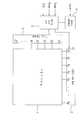
도 6은 본 발명의 실시예에 따른 액정표시장치의 구성 블록도6 is a block diagram illustrating a liquid crystal display according to an exemplary embodiment of the present invention.
도 7은 도 6의 각 쉬프트 레지스터의 회로 구성도7 is a circuit diagram illustrating each shift register of FIG. 6.
도 8은 도 6의 셀 어레이 구성을 나타낸 구성 블록도8 is a block diagram illustrating a cell array configuration of FIG. 6;
도 9a와 도 9b는 본 발명의 게이트 구동을 위한 양방향으로 내장된 게이트 구동회로의 타이밍도9A and 9B are timing diagrams of a gate driving circuit built in both directions for driving a gate of the present invention.
도 10은 본 발명에 따른 데이터라인 및 게이트라인의 출력 타이밍도10 is an output timing diagram of a data line and a gate line according to the present invention.
* 도면의 주요 부분에 대한 부호의 설명 *Explanation of symbols on the main parts of the drawings
60 : 픽셀 어레이부 70 : 제 1 게이트 구동회로60
80 : 제 2 게이트 구동회로80: second gate driving circuit
본 발명은 액정표시장치에 대한 것으로, 특히 양방향 내장 게이트 구동회로를 이용하여 데이터라인의 수를 줄이기에 알맞은 액정표시장치에 관한 것이다.The present invention relates to a liquid crystal display device, and more particularly, to a liquid crystal display device suitable for reducing the number of data lines by using a bidirectional internal gate driving circuit.
정보화 사회가 발전함에 따라 표시장치에 대한 요구도 다양한 형태로 점증하고 있으며, 이에 부응하여 근래에는 LCD(Liquid Crystal Display Device), PDP(Plasma Display Panel), ELD(Electro Luminescent Display), VFD(Vacuum Fluorescent Display)등 여러 가지 평판 표시 장치가 연구되어 왔고 일부는 이미 여러 장비에서 표시장치로 활용되고 있다.As the information society develops, the demand for display devices is increasing in various forms, and in recent years, liquid crystal display devices (LCDs), plasma display panels (PDPs), electro luminescent displays (ELDs), and vacuum fluorescent (VFD) Various flat panel display devices such as displays have been studied, and some of them are already used as display devices in various devices.
그 중에, 현재 화질이 우수하고 경량, 박형, 저소비 전력의 특징 및 장점으로 인하여 이동형 화상 표시장치의 용도로 CRT(Cathode Ray Tube)을 대체하면서 LCD가 가장 많이 사용되고 있으며, 노트북 컴퓨터의 모니터와 같은 이동형의 용도 이외에도 방송신호를 수신하여 디스플레이하는 텔레비전, 및 컴퓨터의 모니터 등으로 다양하게 개발되고 있다.Among them, LCD is the most widely used as the substitute for CRT (Cathode Ray Tube) for mobile image display because of its excellent image quality, light weight, thinness, and low power consumption. In addition to the use of the present invention, a variety of applications such as a television, a computer monitor, and the like for receiving and displaying broadcast signals have been developed.
이하, 일반적인 액정표시장치에 대하여 설명하면 다음과 같다.Hereinafter, a general liquid crystal display device will be described.
도 1은 일반적인 액티브 매트릭스형 액정표시장치의 블록 구성도이다.1 is a block diagram of a general active matrix liquid crystal display device.
화상을 표시하는 부분이 액정표시패널(1)이다. 이 액정표시패널(1)을 구동하기 위한 회로로서, 상기의 수직방향과 수평방향의 각 단부에 각각 신호선 구동회로(2)와 주사선 구동회로(3)가 배치되어 있다. 이들 신호선 구동회로(2) 및 주사선 구동회로(3)를 제어하는 제어신호는 타이밍 발생회로(5)에서 발생된다. 기본적으로는 외부에서 입력되는 수평 동기신호(HSYNC)와 수직 동기신호(VSYNC)와 도트 클럭 (CLK)에서 각종 제어신호가 생성된다. 그리고, 신호선 구동회로(2)의 데이터입력과의 인터페이스 형태에 따라, 지정된 지시대로 정리하는 등의 데이터처리를 실시할 필요가 있으며, 이를 실시하는 것이 데이터 처리회로(4)이며, 이것도 타이밍 발생회로(5)에 의해 제어된다. 통상, 상기의 데이터 처리회로(4)와 타이밍 발생회로(5)는 ASIC에서 하나로 합해져 개발되는 일이 많다.The part which displays an image is the liquid
상술한 바와 같은 액정표시장치는 크게 영상신호를 표시하는 액정표시패널과 외부에서 상기 액정표시패널에 구동신호를 인가하는 구동회로로 구분할 수 있다.The liquid crystal display device as described above may be largely divided into a liquid crystal display panel displaying an image signal and a driving circuit applying a driving signal to the liquid crystal display panel from the outside.
상기 액정표시패널(1)은, 도면에는 도시되지 않았지만, 일정한 공간을 갖고 합착된 두 개의 투명 기판(유리 기판) 사이에 액정이 주입된 표시장치로서, 상기 두개의 투명 기판 중 하나에는 일정 간격으로 배열된 복수개의 게이트 라인(G1,G2,G3,…,Gn)과, 게이트 라인에 수직한 방향으로 일정한 간격을 갖고 배열되는 복수개의 데이터 라인(S1, S2, S3,…,Sn)과, 상기 각 게이트 라인과 데이터 라인에 의해 정의된 매트릭스 형태의 각 픽셀 영역에 형성된 복수개의 픽셀전극과, 상기 게이트 라인의 신호에 따라 상기 데이터 라인의 신호를 각 픽셀전극에 인가하는 복수개의 박막트랜지스터가 상기 각 게이트 라인과 데이터 라인이 교차하는 부분에 형성된다. 그리고 나머지 기판에는 칼라필터층, 공통전극(VCOM) 및 블랙 매트릭스층이 형성된다.Although not shown in the drawing, the liquid
따라서, 게이트 라인에 순차적으로 턴온 신호를 인가하면 그 때마다 해당 라인의 픽셀 전극에 데이터 신호가 인가되므로 영상이 표시된다.Therefore, when the turn-on signal is sequentially applied to the gate line, an image is displayed because the data signal is applied to the pixel electrode of the corresponding line.
상기 구성을 갖는 박막트랜지스터(Thin Film Transistor:TFT)용 LCD는 내부 의 픽셀을 온/오프시키는 스위칭소자로서 TFT를 이용하며, 이 TFT가 온/오프됨에 따라 픽셀들이 온/오프된다.The LCD for thin film transistor (TFT) having the above configuration uses a TFT as a switching element for turning on / off an internal pixel, and the pixels are turned on / off as the TFT is turned on / off.
즉, 일반적인 TFT 액정표시장치는 화소를 구성하는 셀들이 어레이 형태로 배열되어 있고, 각 셀들은 스위칭 기능을 하는 TFT와 액정 셀, 스토리지 커패시터(CSTG)로 구성된다. 그리고, 각 TFT의 소스(source)들이 컬럼(column) 방향으로 공통으로 연결되어 데이터라인(D1~DN)을 형성한 후 소스 드라이버에 연결되어 있고, 각 TFT의 게이트(gate)들이 로우(row) 방향으로 공통으로 연결되어 게이트 라인(G1~GM)을 형성한 후 게이트 드라이버에 연결되어 NxM 해상도(예컨대, SVGA는 800x600, XGA는 1024x768, UXGA는 1600x1200)를 갖는 표시장치를 구현하고 있다.That is, in a typical TFT liquid crystal display device, cells constituting pixels are arranged in an array form, and each cell includes a TFT having a switching function, a liquid crystal cell, and a storage capacitor (CSTG). The sources of the TFTs are commonly connected in a column direction to form data lines D1 to DN, and then connected to a source driver, and gates of the TFTs are rowed. The gate lines G1 to GM are commonly connected to each other to form gate lines G1 to GM, and then connected to the gate driver to implement a display device having NxM resolution (eg, 800x600 for SVGA, 1024x768 for XGA, and 1600x1200 for UXGA).
여기서, 소스 드라이버는 데이터 드라이버, 컬럼 드라이버 또는 신호선 구동회로라고도 하고, 게이트 드라이버는 로우(ROW) 드라이버, 스캔(SCAN) 드라이버 또는 주사선 구동회로라고도 한다. 이하, 소스 드라이버는 신호선 구동회로, 게이트 드라이버는 주사선 구동회로라고 명명하여 설명한다.The source driver may also be referred to as a data driver, column driver, or signal line driver circuit, and the gate driver may also be referred to as a ROW driver, scan driver, or scan line driver circuit. Hereinafter, the source driver will be described as a signal line driver circuit and the gate driver as a scan line driver circuit.
액정 셀은 TFT의 드레인(drain)과 화소전극을 통해 연결되고, 다른 편은 공통전극으로 연결된다. 화소전극은 투명하고 전기 전도성을 갖는 ITO로 만들어지며 TFT 게이트에 온신호가 인가될 때 신호선 구동회로를 통해 인가되는 신호전압을 액정 셀에 가해주고, 공통전극은 역시 ITO로 만들어져 액정 셀에 공통전압(VCOM)을 인가한다. 그리고, 스토리지 커패시터(CSTG)는 화소전극(픽셀 ITO)에 인가된 신호전압을 일정 시간 유지시켜주는 역할을 하며, 충전 및 방전을 통해 액정 셀의 배열 상태를 변화시켜줌으로써 픽셀의 광투과율을 조절한다. 스토리지 커패시터(CSTG)의 일측은 독립 전극이나 게이트 전극과 연결될 수 있는데, 게이트전극과 연결되는 구조를 스토리지 온 게이트(storage on gate)방식이라 한다.The liquid crystal cell is connected to the drain of the TFT through the pixel electrode, and the other side is connected to the common electrode. The pixel electrode is made of transparent and electrically conductive ITO. When the on-signal is applied to the TFT gate, the pixel electrode applies a signal voltage applied through the signal line driver circuit to the liquid crystal cell. The common electrode is also made of ITO, which is common to the liquid crystal cell. Apply (VCOM). The storage capacitor CSTG maintains the signal voltage applied to the pixel electrode ITO and adjusts the light transmittance of the pixel by changing the arrangement state of the liquid crystal cell through charging and discharging. . One side of the storage capacitor CSTG may be connected to an independent electrode or a gate electrode, and a structure connected to the gate electrode is called a storage on gate method.
최근에는 박막 트랜지스터 (이하, TFT 라 함)를 사용한 액정표시장치(LCD)가 노트북 컴퓨터의 디스플레이 등의 용도로 보급되어 가격의 저렴화가 추진되고 있지만, 보다 더 저가격화가 요구되고 있다. 이와 같은 저가격화를 실현하기 위한 하나의 대책으로 부재비의 삭감을 들 수 있는데, 그 중에서도 부재비의 대부분을 차지하는 액정표시패널의 신호선을 구동하는 회로로 사용되는 드라이버 IC의 비용을 내리는 것이 키포인트가 된다. 이 신호선측의 드라이버 IC 가 부재비 중에서 대부분을 차지하는 이유는, 고도의 동작 기능이기 때문에 1개 당의 가격이 높고, 게다가 1개 당 240 출력으로 하면 SVGA 패널에서는 10개가 필요하게 되도록 수를 많이 사용하는 점에 있다. 따라서, 이 드라이버 IC의 수를 줄이는 것이 제안되고 있으며, 예컨대, 일본 공개특허공보 평3-38689호 공보, 일본 공개특허공보 평5-265045 호 공보, 일본 공개특허공보 평6-148680 호 공보에 제안된 것이 있다. 이들은 모두, 액정표시패널의 인접하는 표시화소에서 신호선을 공용하여, 신호선측 드라이버 IC 의 개수를 절반으로 하려고 하는 것이다.In recent years, liquid crystal displays (LCDs) using thin film transistors (hereinafter referred to as TFTs) have been widely used for display in notebook computers and the like. One measure to achieve such a low price is to reduce the member cost. Among them, the key point is to lower the cost of the driver IC used as a circuit for driving the signal line of the liquid crystal display panel, which accounts for the majority of the component cost. do. The reason why the driver IC on the signal line side accounts for most of the absence ratio is because of its high operating function, the price per unit is high, and when 240 outputs per unit are used, a number of 10 units are required in the SVGA panel. Is in point. Therefore, it is proposed to reduce the number of these driver ICs, for example, in Japanese Unexamined Patent Application Publication Nos. Hei 3-38689, Japanese Unexamined Patent Application Publication Nos. 5-265045, and 6-6148680. There is something. In all of these cases, the signal lines are shared by adjacent display pixels of the liquid crystal display panel, so that the number of signal line side driver ICs is halved.
이하, 첨부 도면을 참조하여 상기 신호선 드라이버 IC를 반감하기 위한 종래 기술에 대하여 설명한다.Hereinafter, with reference to the accompanying drawings, a conventional technique for halving the signal line driver IC will be described.
도 2와 도 3은 종래 기술에 따른 액정표시장치의 구성도 및 그 구동 파형도이다.2 and 3 are a configuration diagram and a driving waveform diagram of the liquid crystal display according to the prior art.
먼저, 종래 기술에 따른 액정표시장치는, 도 2에 도시한 바와 같이, 일방향 으로 배열된 복수개의 게이트라인과, 1개의 데이터라인에 짝을 이루어 연결된 2개의 이웃하는 픽셀(제 1, 제 2 픽셀(A,B)(C,D))과, 각 게이트라인의 신호를 받아 턴온/턴오프가 결정되는 제 1 트랜지스터(T1)와, 제 1 트랜지스터(T1)가 턴온될 경우 다음단 게이트라인의 신호를 입력받아 턴온되어 데이터라인을 통해 데이터 신호를 제 1 픽셀로 전달하는 제 2 트랜지스터(T2)와, 다음단 게이트라인의 신호를 받아서 턴온/턴오프되어 제 2 픽셀로 데이터라인을 통해 데이터 신호를 전달하는 제 3 트랜지스터(T3)와, 이전단 게이트라인과 각 픽셀 사이에 연결된 스토리지 커패시터(Cst)로 구성되어 있다.First, as shown in FIG. 2, a liquid crystal display according to the related art includes a plurality of gate lines arranged in one direction and two neighboring pixels connected in pairs to one data line (first and second pixels). (A, B) (C, D)), the first transistor T1 whose turn-on / turn-off is determined in response to the signal of each gate line, and when the first transistor T1 is turned on, The second transistor T2 receives the signal and is turned on to transfer the data signal to the first pixel through the data line, and the signal is turned on / off after receiving the signal of the next gate line, and the data signal through the data line to the second pixel. And a storage transistor Cst connected between the previous gate line and each pixel.
상기의 구성은 1개의 데이터라인을 이용하여 인접한 2개의 픽셀을 구동하기 위한 것으로 데이터 라인 쉐어링(Data Line Sharing:DLS) 구동을 위한 구성이다.The above configuration is used to drive two adjacent pixels using one data line, and is a configuration for driving data line sharing (DLS).
상기 DLS 구동 방식을 이용한 액정표시장치는, 1개의 데이터라인을 이용하여 인접한 2개의 픽셀에 데이터 신호를 인가할 수 있어 구동 IC의 수를 반으로 절감할 수 있다.In the liquid crystal display using the DLS driving method, a data signal may be applied to two adjacent pixels using one data line, thereby reducing the number of driving ICs in half.
상기 액정표시장치의 구동을 위해서는 도 3에 도시한 바와 같이, 1주기의 출력 파형 앞에 반주기의 출력 파형을 갖는 게이트 파형을 이용한다. 즉, DLS 구동을 위해서는 종래의 게이트 구동 파형과는 다른 파형이 필요하며, 1개의 게이트 라인에 인가되는 파형은 2개의 파형으로 구성되어 있고, 앞에 위치하는 파는 뒤따라 오는 파의 반주기의 크기를 갖는다.In order to drive the liquid crystal display, as shown in FIG. 3, a gate waveform having a half-cycle output waveform in front of one cycle of the output waveform is used. That is, a waveform different from the conventional gate driving waveform is required for the DLS driving, and the waveform applied to one gate line is composed of two waveforms, and the wave located in front has a size of a half cycle of the following wave.
도면을 참조하여 구동 원리를 설명하면 다음과 같다.Referring to the drawings the driving principle is as follows.
도 2, 도 3에 도시한 바와 같이 게이트 신호가 G(n), G(n+1), G(n+2)에 순차 적으로 인가될 경우, t1 구간에서는 G(n+1)에 한 주기, G(n+2)에 반주기의 "하이" 신호가 인가되면, G(n+1) 신호를 받아 제 1, 제 3 트랜지스터(T1,T3)가 턴온되고, G(n+1)이 턴온됨에 따라 G(n+2) 신호를 받은 제 2 트랜지스터(T2)도 턴온된다. 이에 따라서 제 1, 제 2 픽셀(A,B)에 동시에 데이터 신호가 인가된다.As shown in FIGS. 2 and 3, when the gate signal is sequentially applied to G (n), G (n + 1), and G (n + 2), the gate signal is limited to G (n + 1) in the t1 section. When a half period "high" signal is applied to the period, G (n + 2), the first and third transistors T1 and T3 are turned on by receiving the G (n + 1) signal, and G (n + 1) is turned on. As turned on, the second transistor T2 receiving the G (n + 2) signal is also turned on. Accordingly, the data signal is applied to the first and second pixels A and B simultaneously.
이후에 반주기 시간이 경과한 t2구간에서는 제 2 트랜지스터(T2)는 턴오프되고, 제 1, 제 3 트랜지스터(T1,T3)는 턴온된 상태이므로 제 1 픽셀(A)에는 이미 인가된 데이터 신호만이 남게 되고, 제 2 픽셀(B)에는 다른 데이터 신호를 인가시킬 수 있다.Afterwards, the second transistor T2 is turned off and the first and third transistors T1 and T3 are turned on in the period t2 after the half cycle time has elapsed. Therefore, only the data signal already applied to the first pixel A is turned on. Is left, and another data signal can be applied to the second pixel (B).
따라서 1개의 데이터 라인을 이용하여 2개의 이웃하는 픽셀에 순차적으로 서로 다른 2개의 데이터 신호를 인가할 수 있다.Accordingly, two different data signals may be sequentially applied to two neighboring pixels by using one data line.
상기에서와 같이 반주기의 다음단 게이트 신호를 이용하여 선택적으로 이웃하는 서로 다른 픽셀에 데이터 신호를 인가할 수 있으며, 이러한 방법으로 구동시킬 경우 1개의 데이터라인에 1픽셀을 연결하던 일반적인 데이터 구동 방법에 비하여 데이터 라인의 수를 절반으로 줄일 수 있어 구동을 위한 데이터 IC의 채널 수를 반감할 수 있다.As described above, a data signal may be selectively applied to different neighboring pixels by using a gate signal of a next stage of a half period. When driving in this manner, a general data driving method in which one pixel is connected to one data line is used. In comparison, the number of data lines can be reduced in half, which can reduce the number of channels of the data IC to drive.
그러나, 데이터 라인 쉐어링(DLS) 방법을 적용하기 위해서는, 일반적인 출력 파형이 아닌 반주기 출력과 한주기 출력이 연속적으로 나오는 특이한 게이트 파형을 출력할 수 있는 별도의 구동 IC를 구비시켜야 한다. 따라서 데이터 라인의 수를 반감하더라도 별도의 게이트 구동 IC를 구비시켜야 하므로 제조 원가를 줄이는데는 한계가 있다.However, in order to apply the data line sharing (DLS) method, it is necessary to provide a separate driving IC capable of outputting a unique gate waveform in which a half-cycle output and a single-cycle output are continuous instead of a general output waveform. Therefore, even if the number of data lines is halved, a separate gate driver IC must be provided, which reduces the manufacturing cost.
다음에, 종래의 다른 기술에 따른 액정표시장치에 대하여 설명한다.Next, a liquid crystal display device according to another conventional technique will be described.
도 4와 도 5는 종래의 다른 기술에 따른 액정표시장치의 회로 구성도 및 그 구동 파형도이다.4 and 5 are circuit configuration diagrams and driving waveform diagrams of a liquid crystal display according to another conventional technology.
종래의 다른 기술에 따른 액정표시장치는, 도 4에 도시한 바와 같이, 액정표시패널은 n 열 × m 행의 화소전극으로 구성된다 (n, m 은 각각 2 이상의 정수). 그리고, 수평방향(행방향)의 홀수번째 픽셀과 짝수번째 픽셀이 서로 인접하는 픽셀에서, 수직방향(열방향)으로 신장한 1개의 데이터라인을 공용하고 있으며, 각 픽셀에 접속되는 스위칭소자인 TFT의 드레인이 접속되어 있다. 즉, 데이터라인의 수는 수평방향의 픽셀수의 절반(n/2 개)이 된다. 상기의 인접하는 2개의 TFT의 게이트는 홀수번째의 TFT와 짝수번째의 TFT로, 수평방향의 1표시라인에 할당된 수평방향으로 신장하는 2개의 게이트라인의 각각 다른 게이트라인에 접속되어 있다. 따라서, 게이트라인의 수는 수직방향의 픽셀수의 배 (2m개)가 된다.In the conventional liquid crystal display device according to another technique, as shown in Fig. 4, the liquid crystal display panel is constituted by pixel electrodes of n columns x m rows (n and m are integers of 2 or more, respectively). Then, in a pixel in which the odd-numbered pixels and the even-numbered pixels in the horizontal direction (row direction) are adjacent to each other, one data line extending in the vertical direction (column direction) is shared, and a TFT which is a switching element connected to each pixel is used. The drain of is connected. That is, the number of data lines is half (n / 2) of the number of pixels in the horizontal direction. The gates of the two adjacent TFTs are odd-numbered TFTs and even-numbered TFTs, and are connected to different gate lines of two gate lines extending in the horizontal direction assigned to one display line in the horizontal direction. Therefore, the number of gate lines is twice the number of pixels in the vertical direction (2 m).
그러나, 상기 구성에서는, 홀수행째의 표시라인에서는, 수평방향의 홀수번째 픽셀의 TFT의 게이트는 홀수행째의 게이트라인에 접속되고, 수평방향의 짝수번째 픽셀의 TFT 의 게이트는 짝수행째의 게이트라인에 접속된다. 또한, 짝수행째의 표시라인에서는, 수평방향의 홀수번째 픽셀의 TFT의 게이트는 짝수행째의 게이트라인에 접속되고, 수평방향의 짝수번째 픽셀의 TFT의 게이트는 홀수행째의 게이트라인에 접속된다. 즉, 수평방향의 임의의 표시라인에 주목한 경우, 그 표시라인에 할당되는 복수개의 게이트라인에서, 수평방향 홀수번째의 TFT의 게이트는 어느 한쪽의 게이트라인에 접속되어 있으며, 짝수번째의 TFT 의 게이트는 다른 한쪽의 게이트라 인에 접속되어 있다. 그리고, 그 표시라인에 인접하는 표시라인에서는, 상기의 TFT의 게이트와 게이트라인의 접속은 반대관계에 있다. 다시 말하면, 홀수번째의 표시라인과 짝수번째의 표시라인에서, TFT의 게이트와 게이트라인의 접속관계가 반대라는 것이다.However, in the above arrangement, in the odd-numbered display lines, the gates of the TFTs in the odd odd pixels in the horizontal direction are connected to the gate lines in the odd rows, and the gates of the TFTs in the even pixels in the horizontal direction are connected to the gate lines in the even rows. Connected. Further, in the even-numbered display lines, the gates of the TFTs of the odd-numbered pixels in the horizontal direction are connected to the even-line gate lines, and the gates of the TFTs of the even-numbered pixels in the horizontal direction are connected to the gate lines of the odd-numbered rows. That is, when attention is paid to any display line in the horizontal direction, in a plurality of gate lines assigned to the display line, the gates of the horizontal odd-numbered TFTs are connected to either gate line, The gate is connected to the other gate line. In the display line adjacent to the display line, the connection between the gate of the TFT and the gate line is in the opposite relationship. In other words, in the odd-numbered display lines and the even-numbered display lines, the connection relationship between the gates of the TFTs and the gate lines is reversed.
상기의 구성을 갖을 때 동작을 도 5의 타이밍도를 참조하여 설명한다.An operation when having the above configuration will be described with reference to the timing chart of FIG.
도 5에 도시한 바와 같이, 시리얼로 입력되어 오는 데이터를 데이터 처리회로(미도시)로 받아, 데이터 처리회로에 형성되어 있는 라인메모리에 1 라인 분을 기입하고, 패널의 TFT 와 데이터라인, 게이트라인의 접속에 따라, 데이터를 1 수평기간(1H)의 절반으로 전반과 후반으로 나눈다.As shown in Fig. 5, data input in serial is received by a data processing circuit (not shown), and one line is written into the line memory formed in the data processing circuit, and the TFT, data line, and gate of the panel are written. Depending on the connection of the line, the data is divided into first half and second half of one horizontal period (1H).
즉, 패널 1행째의 표시라인(m=1)에서, 전반에 출력되는 데이터는, 홀수번째의 데이터에서 S1, S3, S5, … 가 된다. 이것을 A 패턴이라 한다. 후반에 출력되는 데이터는 짝수번째의 데이터에서 S2, S4, S6, … 이 된다. 이것을 B 패턴이라 한다.In other words, in the display line (m = 1) of the first row of the panel, the data output in the first half is S1, S3, S5,... Becomes This is called an A pattern. The data output in the second half is S2, S4, S6, ... in the even data. Becomes This is called a B pattern.
2행째의 표시라인(m=2) 에서는, 반대로 전반이 B 패턴, 후반이 A 패턴이 된다. 3 행째의 표시라인 이후는, 이 1, 2 행째의 반복으로, 데이터라인에 출력된다. 이와 같이 데이터가 데이터라인에 출력되면, 게이트라인은 순차적으로 G1, G2, G3, … 로 TFT 의 ON 전압을 시프트해 가면, 소정의 픽셀에 소정의 데이터가 기입되게 된다.In the display line m = 2 of the 2nd line, the first half becomes a B pattern and the second half becomes an A pattern. After the display line of the third row, the first and second rows are output to the data line. When data is output to the data line in this way, the gate lines are sequentially G1, G2, G3,... By shifting the ON voltage of the TFT, predetermined data is written to a predetermined pixel.
예컨대, 데이터라인(S1)에 주목하면, 게이트라인이 순차적으로 G1부터 ON되면, d11(A), d12(B), d22(B), d21(A) … 로 데이터는 기입된다. 상기에서 (A), (B) 는 A 패턴, B 패턴을 의미한다.For example, paying attention to the data line S1, when the gate lines are sequentially turned on from G1, d11 (A), d12 (B), d22 (B), d21 (A). The data is written to. In the above, (A) and (B) means A pattern and B pattern.
여기에서 신호선 구동회로에서 출력되는 신호의 극성은, 인접하는 출력끼리가 서로 반대극성으로 1 회의 출력마다 극성반전하는 것을 고려하면, 1 프레임 기입 종료후의 화면상의 극성은 수평방향은 2 픽셀 간격, 수직방향은 1 픽셀 간격으로 극성이 반전한다. 이것은 상기한 모든 인접 픽셀에 대하여 반대극성의 관계가 되는 도트 반전 구동과는 약간 다르지만, 2개를 1조로 하는 인접 픽셀 관계에서 보면 반대극성으로 되어, 양극성과 음극성의 차이에 의한 플리커 (flicker, 어른거림)에 강하다고 할 수 있다.Here, considering that the polarities of the signals output from the signal line driver circuit are reversed in polarity for each output with adjacent polarities opposite to each other, the polarity on the screen after completion of one frame writing is two pixel intervals in the horizontal direction and vertical. The direction is reversed in polarity by 1 pixel intervals. This is slightly different from the dot inversion driving which has the opposite polarity relation to all the above-mentioned adjacent pixels, but becomes the opposite polarity in the adjacent pixel relationship of two sets, and flicker due to the difference between the polarity and the negative polarity. Strong).
상기에서와 같이 종래 다른 기술에 따른 액정표시장치는 2개의 게이트라인을 사용하여 각 라인의 홀수번째 픽셀과 짝수번째 픽셀을 구동하는 것에 특징이 있다.As described above, the liquid crystal display according to another conventional technology is characterized by driving odd pixels and even pixels of each line using two gate lines.
상기와 같이 1표시라인을 2개의 게이트라인을 사용하여 구동하기 위해서는 1개의 게이트라인을 사용하여 구동하는 액정표시장치와 비교하여 2배의 게이트라인이 필요하다. 이에 따라서 1프레임동안 2배의 게이트라인을 모두 구동시키기 위해서는 1픽셀 충전시간이 1H에서 H/2로 감소하게 되므로 충분한 픽셀 유효 충전시간의 확보가 어렵다는 문제가 있다.As described above, in order to drive one display line using two gate lines, a gate line twice as much as that of a liquid crystal display device using one gate line is required. Accordingly, in order to drive all of the gate lines twice as large as one frame, one pixel charge time is reduced from 1H to H / 2. Therefore, it is difficult to secure sufficient pixel effective charge time.
본 발명은 상기와 같은 문제를 해결하기 위하여 안출한 것으로, 본 발명의 목적은 양방향 내장 게이트 구동회로를 이용하여 픽셀 유효 충전 시간을 줄이지 않으면서 데이터 라인의 수를 반감시킬 수 있는 액정표시장치 및 그의 구동방법을 제공하는데 있다.SUMMARY OF THE INVENTION The present invention has been made to solve the above problems, and an object of the present invention is to provide a liquid crystal display device capable of halving the number of data lines without reducing the pixel effective charging time by using a bidirectional built-in gate driving circuit. It is to provide a driving method.
상기와 같은 목적을 달성하기 위한 본 발명에 따른 액정표시장치는 하부기판상에 수평방향으로 배열된 인접한 픽셀이 같은 데이터라인을 공유하도록 쌍을 이루고 있는 복수개의 픽셀들을 구비한 픽셀 어레이부와; 상기 픽셀 어레이부의 좌,우 양측에 독립적으로 구동하도록, 제 1 내지 제 n 홀수 쉬프트 레지스터로 구성된 제 1 게이트 구동회로와, 제 1 내지 제 n 짝수 쉬프트 레지스터로 구성된 제 2 게이트 구동회로를 포함함을 특징으로 한다.According to an aspect of the present invention, there is provided a liquid crystal display device including: a pixel array unit including a plurality of pixels paired so that adjacent pixels arranged in a horizontal direction on a lower substrate share the same data line; And a first gate driving circuit composed of first to nth odd shift registers and a second gate driving circuit composed of first to nth even shift registers to independently drive left and right sides of the pixel array unit. It features.
상기 픽셀 어레이부는 수평방향(행방향)의 홀수번째 픽셀과 짝수번째 픽셀이 서로 인접하여 한쌍을 이루고 있고, 상기 수평방향으로 인접한 한쌍의 픽셀은 수직방향(열방향)으로 배열된 1개의 데이터라인을 공용하고 있으며, 상기 수평방향의 픽셀들 사이에는 홀수번째와 짝수번째의 2개의 게이트라인이 일방향으로 배열되어 있음을 특징으로 한다.The pixel array unit forms a pair of odd-numbered pixels and even-numbered pixels in a horizontal direction (row direction) adjacent to each other, and the pair of pixels adjacent in the horizontal direction forms one data line arranged in a vertical direction (column direction). In common, two odd-numbered and even-numbered gate lines are arranged in one direction between the pixels in the horizontal direction.
상기 각 픽셀에는 데이터 신호를 인가시키기 위한 스위칭소자(TFT)가 각각 접속되어 있고, 상기 스위칭소자(TFT)의 드레인전극은 데이터라인에 접속되어 있고, 소오스전극은 각 픽셀 전극에 접속되어 있음을 특징으로 한다.Each pixel is connected to a switching element TFT for applying a data signal, a drain electrode of the switching element TFT is connected to a data line, and a source electrode is connected to each pixel electrode. It is done.
상기 데이터라인의 수는 수평방향의 픽셀수의 절반임을 특징으로 한다.The number of data lines is half the number of pixels in the horizontal direction.
상기 제 1 내지 제 n 홀수 쉬프트 레지스터는 상기 픽셀 어레이부의 각 홀수번째(Odd) 게이트라인에 게이트 신호를 출력하도록 구성됨을 특징으로 한다.The first to nth odd shift registers may be configured to output a gate signal to each odd-numbered gate line of the pixel array unit.
상기 제 1 내지 제 n 짝수 쉬프트 레지스터는 상기 픽셀 어레이부의 각 짝수번째(Even) 게이트라인에 게이트 신호를 출력하도록 구성됨을 특징으로 한다.The first to nth even shift registers may be configured to output a gate signal to each even gate line of the pixel array unit.
상기 각 쉬프트 레지스터는, Vst 또는 이전단 쉬프트 레지스터의 출력 신호를 입력받아서 턴온 여부가 결정되며 상기 Vst 또는 이전단 쉬프트 레지스터의 출력 신호와 Q노드 사이에 다이오드 커넥팅된 제 1 트랜지스터(T11)와, 상기 Vst 또는 이전단 쉬프트 레지스터의 출력 신호를 입력받아서 턴온 여부가 결정되며 일단이 접지전압단(Vss) 사이에 연결된 제 2 트랜지스터(T12)와, 상기 Q노드의 신호를 입력받아 턴온 여부가 결정되며 일단이 접지전압단 사이에 연결된 제 3 트랜지스터(T13)로 구성된 풀업 구동부와; 상기 Q노드의 신호를 입력받아서 턴온 여부가 결정되며 제 1 또는 제 2 클럭 신호(C1 or C2) 입력단과 게이트 출력 신호단(G) 사이에 연결된 제 4 트랜지스터(T14)로 구성된 풀업부와; 제 1 또는 제 2 클럭바신호(C1B or C2B)를 입력받아서 턴온 여부가 결정되며 Vdd와 QB노드 사이에 연결된 제 5 트랜지스터(T15)와, 상기 QB노드의 신호를 입력받아서 턴온 여부가 결정되며 Q와 접지전압단 사이에 연결된 제 6 트랜지스터(T16)와, 다음단 출력을 입력 받아서 턴온 여부가 결정되며 상기 Q노드와 접지전압단(Vss) 사이에 연결된 제 7 트랜지스터(T17)로 구성된 풀다운 구동부와; 상기 QB노드 신호를 입력받아서 턴온 여부가 결정되며 상기 게이트 출력 신호단(G)과 접지전압단 사이에 연결된 제 8 트랜지스터(T18)로 구성된 풀다운부로 구성됨을 특징으로 한다.Each of the shift registers may include a first transistor T11 diode-connected between the output signal of the Vst or previous shift register and a Q node and determined to be turned on by receiving the output signal of the Vst or previous shift register. It is determined whether to turn on by receiving the output signal of Vst or the previous shift register, and whether or not it is turned on by receiving the signal of the Q node and the second transistor T12 connected between the ground voltage terminal Vss. A pull-up driver composed of a third transistor T13 connected between the ground voltage terminals; A pull-up unit configured to receive a signal of the Q node and determine whether to turn it on, and including a fourth transistor T14 connected between an input terminal of a first or second clock signal C1 or C2 and a gate output signal terminal G; It is determined whether to turn on by receiving the first or second clock bar signal C1B or C2B, and whether it is turned on by receiving the signal of the QB node and the fifth transistor T15 connected between the Vdd and QB nodes. A pull-down driving unit configured to receive a sixth transistor T16 connected between the ground terminal and a ground voltage terminal, and to receive the next stage output and to turn on the seventh transistor T17 connected between the Q node and the ground voltage terminal Vss; ; It is characterized in that it is composed of a pull-down unit consisting of an eighth transistor (T18) connected between the gate output signal terminal (G) and the ground voltage terminal is determined by receiving the QB node signal is turned on.
상기 쉬프트 레지스터의 각 트랜지스터는 비정질 실리콘 트랜지스터로 구성됨을 특징으로 한다.Each transistor of the shift register is characterized by consisting of an amorphous silicon transistor.
상기 구성을 갖는 본 발명에 따른 액정표시장치의 구동방법은 하부기판 상에 수평방향(행방향)의 홀수번째 픽셀과 짝수번째 픽셀이 서로 인접하여 한쌍을 이루 고 있고, 상기 수평방향으로 인접한 한쌍의 픽셀은 수직방향(열방향)으로 배열된 1개의 데이터라인을 공용하고 있으며, 상기 수평방향의 픽셀들 사이에는 홀수번째와 짝수번째의 2개의 게이트라인이 일방향으로 배열되어 있는 픽셀 어레이부와, 상기 픽셀 어레이부의 좌,우 양측에 구성되며, 제 1 내지 제 n 홀수 쉬프트 레지스터로 구성된 제 1 게이트 구동회로와, 제 1 내지 제 n 짝수 쉬프트 레지스터로 구성된 제 2 게이트 구동회로를 포함하여 구성된 액정표시장치의 구동방법에 있어서, 상기 제 1, 제 2 게이트 구동회로는 H/2의 시간 차이를 두고 제 1, 제 2 클럭신호(C1,C2)를 입력받아서 상기 픽셀 어레이부의 각 짝수번째 및 홀수번째 게이트라인에 각각 H/2의 시간차가 나는 게이트 출력 신호(G1_odd, G1_even)(G2_odd, G2_even),~,(GN_odd, GN_even)들을 독립적으로 출력시킴을 특징으로 한다.In the driving method of the liquid crystal display according to the present invention having the above-described configuration, odd-numbered pixels and even-numbered pixels in a horizontal direction (row direction) are adjacent to each other on a lower substrate to form a pair, and a pair of adjacent in the horizontal direction Pixels share one data line arranged in a vertical direction (column direction), and pixel array units in which two odd and even gate lines are arranged in one direction between the horizontal pixels; A liquid crystal display device including a first gate driving circuit configured on the left and right sides of the pixel array unit, the first gate driving circuit including first to nth odd shift registers, and a second gate driving circuit configured on the first to nth even shift registers. The first and second gate driving circuits of the first and second gate driving circuits receive the first and second clock signals C1 and C2 with a time difference of H / 2, and pick the same. And in that each time difference of H / 2 for each array portion even-numbered and odd-numbered gate lines, I gate output signal (G1_odd, G1_even) (G2_odd, G2_even), ~, characterized by (GN_odd, GN_even) Sikkim the independent output.
이하, 첨부 도면을 참조하여 본 발명의 바람직한 실시예에 따른 액정표시장치 및 그의 구동방법에 대하여 설명하면 다음과 같다.Hereinafter, a liquid crystal display and a driving method thereof according to exemplary embodiments of the present invention will be described with reference to the accompanying drawings.
도 6은 본 발명의 실시예에 따른 액정표시장치의 구성 블록도이고, 도 7은 도 6의 각 쉬프트 레지스터의 회로 구성도이며, 도 8은 도 6의 셀 어레이 구성을 나타낸 구성 블록도이다.6 is a block diagram illustrating a liquid crystal display according to an exemplary embodiment of the present invention, FIG. 7 is a circuit diagram illustrating each shift register of FIG. 6, and FIG. 8 is a block diagram illustrating a cell array configuration of FIG. 6.
본 발명의 일실시예에 따른 액정표시장치는, 하부기판의 좌우 양측 상부에 게이트 구동회로가 내장되어 있으며, 데이터 라인 쉐어링(Data Line Sharing:DLS) 기술을 구현하기 위한 것으로, 도 6에 도시한 바와 같이, 픽셀 어레이부(60)와, 상기 픽셀 어레이부(60)의 좌우 양측에 각각 배치된 제 1, 제 2 게이트 구동회로(70,80)로 구성된다.According to an exemplary embodiment of the present invention, a liquid crystal display device includes gate driving circuits formed on upper and left sides of a lower substrate, and implements data line sharing (DLS) technology. As described above, the
상기 픽셀 어레이부(60)는 도 8에 도시된 바와 같이, 수평방향(행방향)의 홀수번째 픽셀과 짝수번째 픽셀이 서로 인접하여 한쌍을 이루고 있고, 상기 수평방향으로 인접한 한쌍의 픽셀은 수직방향(열방향)으로 배열된 1개의 데이터라인을 공용하고 있으며, 상기 수평방향의 픽셀들 사이에는 홀수번째와 짝수번째의 2개의 게이트라인이 일방향으로 배열되어 있다.As illustrated in FIG. 8, the
각 픽셀에는 데이터 신호를 인가시키기 위한 스위칭소자(TFT)가 각각 접속되어 있고, 스위칭소자(TFT)의 드레인전극은 데이터라인에 접속되어 있고, 소오스전극은 각 픽셀 전극에 접속되어 있다. 즉, 상기 픽셀에 접속된 각각의 스위칭소자(TFT)는 수평방향의 홀수번째 픽셀의 TFT와 짝수번째 픽셀의 TFT로, 수평방향의 1표시라인에 할당된 홀수번째와 짝수번째 게이트라인에 각각 접속되어 있다. 따라서, 게이트라인의 수는 수직방향의 픽셀수의 배가 된다.Each pixel is connected with a switching element TFT for applying a data signal, a drain electrode of the switching element TFT is connected to a data line, and a source electrode is connected to each pixel electrode. That is, each switching element TFT connected to the pixel is a TFT of an odd pixel in the horizontal direction and a TFT of an even pixel, and is connected to odd and even gate lines assigned to one display line in the horizontal direction, respectively. It is. Therefore, the number of gate lines is doubled the number of pixels in the vertical direction.
또한, 상기와 같이 수평방향으로 인접한 한쌍의 픽셀이 수직방향(열방향)으로 배열된 1개의 데이터라인을 공용하고 있으면, 데이터라인의 수는 수평방향의 픽셀수의 절반이 된다.In addition, if a pair of pixels adjacent in the horizontal direction share one data line arranged in the vertical direction (column direction) as described above, the number of data lines is half the number of pixels in the horizontal direction.
그리고 제 1, 제 2 게이트 구동회로(70, 80)는 하부기판의 좌,우측에 내장되어 있으며, 각각 상기 픽셀 어레이부(60)의 홀수번째(Odd)와 짝수번째(Even) 픽셀에 독립적으로 게이트 구동신호를 인가하도록 구성되어 있다.In addition, the first and second
이때 제 1 게이트 구동회로(70)에는 Vst의 스캔 개시 신호와, C1과 C1B의 2상의 클럭신호와, VDD와 VSS 신호가 인가되고, 제 2 게이트 구동회로(80)에는 Vst의 스캔 개시 신호와, C2과 C2B의 2상의 클럭신호와, VDD와 VSS 신호가 인가되어 있다.At this time, the scan start signal of Vst, the clock signals of two phases of C1 and C1B, the VDD and VSS signals are applied to the first
상기에서 픽셀 어레이부(60) 좌,우 양측의 하부기판에 내장된 제 1, 제 2 게이트 구동회로(70, 80)는 각각 제 1 내지 제 n 홀수 쉬프트 레지스터(70_1,~,70_n)와, 제 1 내지 제 n 짝수 쉬프트 레지스터(80_1,~,80_n)로 구성되며, 각 게이트 구동회로를 구성하는 각 쉬프트 레지스터는 비정질 실리콘 트랜지스터로 구현된다.The first and second
상기 제 1 내지 제 n 홀수 쉬프트 레지스터(70_1,~,70_n)는 픽셀 어레이부(60)의 각 홀수번째(Odd) 게이트라인에 게이트 신호를 출력하고, 스캔 개시 신호(Vst) 또는 이전단 쉬프트 레지스터의 출력 신호와, C1과 C1B의 2상의 클럭신호와, VDD와 VSS 신호를 받아 동작한다. 이때 상기 제 1 홀수 쉬프트 레지스터(70_1)는 스캔 개시 신호(Vst)를 받아 구동하도록 구성되었고, 상기 제 2 홀수 쉬프트 레지스터 내지 제 n 홀수 쉬프트 레지스터(70_2,…,70_n)는 순차적으로 이전단 쉬프트 레지스터의 출력 신호를 받아 구동하도록 구성되어 있다.The first to nth odd shift registers 70_1 to 70_n output a gate signal to each odd-numbered gate line of the
그리고 제 1 내지 제 n 짝수 쉬프트 레지스터(80_1,~,80_n)는 픽셀 어레이부(60)의 각 짝수번째(Even) 게이트라인에 게이트 신호를 출력하고, 스캔 개시 신호(Vst) 또는 이전단의 쉬프트 레지스터의 신호와, C2과 C2B의 2상의 클럭신호와, VDD와 VSS 신호를 받아 동작한다. 이때 상기 제 1 짝수 쉬프트 레지스터(70_1)는 스캔 개시 신호(Vst)를 받아 구동하도록 구성되었고, 상기 제 2 짝수 쉬프트 레지스터 내지 제 n 짝수 쉬프트 레지스터(80_2,…,80_n)는 순차적으로 이전단 쉬프트 레지스터의 출력 신호를 받아 구동하도록 구성되어 있다.The first to nth even shift registers 80_1 to 80_n output a gate signal to each even gate line of the
상기 제 1 내지 제 n 홀수 및 짝수 쉬프트 레지스터는, 도 7에 도시된 바와 같이, 제 1 내지 제 8 트랜지스터(T11~T18)로 구성되어 있는데, 각각 풀업 구동부와 풀다운 구동부와 풀업부와 풀다운부로 구성되어 있다. 그리고 제 1 내지 제 8 트랜지스터(T11~T18)은 비정질 실리콘 트랜지스터로 구성되어 있다.As shown in FIG. 7, the first to nth odd-numbered and even-shift registers include first to eighth transistors T11 to T18, and each includes a pull-up driver, a pull-down driver, a pull-up unit, and a pull-down unit. It is. The first to eighth transistors T11 to T18 are composed of amorphous silicon transistors.
풀업 구동부는 Vst 또는 이전단 쉬프트 레지스터의 출력 신호(이하, Vst를 예로 설명한다.)를 입력받아서 턴온 여부가 결정되며 Vst와 Q노드 사이에 다이오드 커넥팅된 제 1 트랜지스터(T11)와, Vst을 입력받아서 턴온 여부가 결정되며 일단이 접지전압단(Vss) 사이에 연결된 제 2 트랜지스터(T12)와, 상기 Q노드의 신호를 입력받아 턴온 여부가 결정되며 일단이 접지전압단 사이에 연결된 제 3 트랜지스터(T13)로 구성된다.The pull-up driver determines whether to turn on by receiving an output signal of Vst or a previous shift register (hereinafter, Vst is described as an example), and inputs the first transistor T11 diode-connected between Vst and Q nodes, and Vst. The second transistor T12 connected to the ground voltage terminal Vss and one of the third transistors connected to the ground voltage terminal. T13).
그리고 풀업부는 Q노드의 신호를 입력받아서 턴온 여부가 결정되며 제 1 또는 제 2 클럭 신호(C1,C2) 입력단과 게이트 출력 신호단(G) 사이에 연결된 제 4 트랜지스터(T14)로 구성된다.In addition, the pull-up unit receives a signal of the Q node to determine whether to turn on, and includes a fourth transistor T14 connected between the input terminal of the first or second clock signals C1 and C2 and the gate output signal terminal G.
그리고 풀다운 구동부는 제 1 또는 제 2 클럭바신호(C1B,C2B)를 입력받아서 턴온 여부가 결정되며 Vdd와 QB노드 사이에 연결된 제 5 트랜지스터(T15)와, QB노드의 신호를 입력받아서 턴온 여부가 결정되며 Q와 접지전압단 사이에 연결된 제 6 트랜지스터(T16)와, 다음단 출력을 입력 받아서 턴온 여부가 결정되며 Q노드와 접지전압단(Vss) 사이에 연결된 제 7 트랜지스터(T17)로 구성된다.In addition, the pull-down driving unit receives the first or second clock bar signals C1B and C2B to determine whether to turn it on, and whether the fifth transistor T15 connected between Vdd and the QB node and the signal of the QB node to turn it on turns on. And a sixth transistor T16 connected between the Q and the ground voltage terminals, and a turn-on being determined by receiving the output of the next stage, and the seventh transistor T17 connected between the Q node and the ground voltage terminal Vss. .
그리고 풀다운부는 QB노드 신호를 입력받아서 턴온 여부가 결정되며 게이트 출력 신호단(G)과 접지전압단 사이에 연결된 제 8 트랜지스터(T18)로 구성된다.The pull-down part receives the QB node signal and determines whether to turn it on. The pull-down part includes an eighth transistor T18 connected between the gate output signal terminal G and the ground voltage terminal.
상기에서 제 1, 제 2 게이트 구동회로(70,80)를 구성하는 도 7에 도시된 각 쉬프트 레지스터의 회로 구성은 일예로써, 이와 다른 다양한 회로적 구성이 가능하다.The circuit configuration of each shift register shown in FIG. 7 constituting the first and second
이하, 상기 구성을 갖는 본 발명의 실시예에 따른 액정표시장치의 구동방법에 대하여 설명하기로 한다.Hereinafter, a driving method of a liquid crystal display device according to an exemplary embodiment of the present invention having the above configuration will be described.
도 9a와 도 9b는 본 발명의 게이트 구동을 위한 양방향으로 내장된 게이트 구동회로의 타이밍도이고, 도 10은 본 발명에 따른 데이터라인 및 게이트라인의 출력 타이밍도이다.9A and 9B are timing diagrams of a bidirectional embedded gate driving circuit for driving a gate of the present invention, and FIG. 10 is an output timing diagram of a data line and a gate line according to the present invention.
상기 구성을 갖는 본 발명의 실시예에 따른 액정표시장치는, 수평방향으로 배열된 픽셀 사이에 배열된 홀수번째와 짝수번째의 2개의 게이트라인이 내장된 2개의 제 1, 제 2 게이트 구동회로(70, 80)에 의해 순차 구동하는데, 이때 제 1, 제 2 게이트 구동회로(70, 80)는 각각 홀수번째와 짝수번째 픽셀을 독립적으로 구동시킨다.The liquid crystal display according to the exemplary embodiment of the present invention having the above structure includes two first and second gate driving circuits in which two odd-numbered and even-numbered gate lines are arranged between pixels arranged in a horizontal direction. 70 and 80 are sequentially driven, wherein the first and second
예를 들어 제 1 홀수 쉬프트 레지스터(70_1)의 출력 신호를 받아서 수평 방향의 첫 번째 라인의 홀수번째 픽셀들이 구동되고, 다음에 제 2 짝수 쉬프트 레지스터(80_1)의 출력 신호를 받아서 첫 번째 라인의 짝수번째 픽셀들이 구동된다.For example, the odd-numbered pixels of the first line in the horizontal direction are driven by receiving the output signal of the first odd shift register 70_1, and then the output signal of the second even-shift register 80_1 is received, and the even-numbered lines of the first line are received. Pixels are driven.
좀더 자세히 설명하면, 도 9a와 도 9b, 도 10에 도시한 바와 같이, 제 1, 제 2 게이트 구동회로(70, 80)를 구성시키기 위한 제 1, 제 2 클럭신호(C1,C2)는 H/2의 시간 차이를 두고 입력되어 H/2의 시간차가 나는 게이트 출력 신호((G1_odd, G1_even)(G2_odd, G2_even),~,(GN_odd, GN_even))를 발생시킨다. 이때 제 1 게이트 구동회로(70)는 Vst, C1, C1B, Vdd, Vss 신호를 받아 구동하고, 제 2 게이트 구동 회로(80)는 Vst, C2, C2B, Vdd, Vss의 신호에 의해 구동한다.In more detail, as shown in FIGS. 9A, 9B, and 10, the first and second clock signals C1 and C2 for configuring the first and second
예를 들어, 제 1 게이트 구동회로(70)로부터 픽셀 어레이부(60)의 제 1 홀수번째 게이트라인에 G1_odd 신호가 입력되는 경우, 첫 번째 수평 라인의 홀수번째 픽셀들(R11O, R12O,~,R1NO)에 연결된 스위칭 소자(TFT)들이 턴온되고, 턴오된 스위칭 소자(TFT)를 통해 데이터 신호가 각 홀수번째 픽셀들(R11O, R12O,~,R1NO)에 기록된다.For example, when the G1_odd signal is input from the first
이후에 H/2 시간 후, 제 2 게이트 구동회로(80)로부터 픽셀 어레이부(60)의 제 1 짝수번째 게이트라인에 G1_even 신호가 입력되는 경우, 첫 번째 수평 라인의 짝수번째 픽셀들(R11E, R12E,~,R1NE)에 연결된 스위칭 소자(TFT)들이 턴온되고, 턴온된 스위칭소자들을 통해 데이터 신호가 각 짝수번째 픽셀들(R11E, R12E,~,R1NE)에 기록된다.After the H / 2 time, when the G1_even signal is input from the second
상기와 같은 방법으로 픽셀 어레이부의 각 픽셀들에 데이터가 기록된다.In the same manner as described above, data is recorded in each pixel of the pixel array unit.
이와 같이 픽셀 어레이부의 좌,우 양측에 독립적으로 구동하는 제 1, 제 2 게이트 구동회로(70, 80)가 내장되어 있고 이를 이용하여 구동시킬 경우, 데이터 라인 쉐어링(DLS)에 따른 게이트 구동회로의 구동속도를 별도로 증가시킬 필요가 없다.As described above, the first and second
부연 설명하면, 종래에는 데이터 라인 쉐어링(DLS) 구동을 할 경우, 게이트 라인이 2배로 증가함에 따라 1프레임동안 구동해야 하는 게이트 구동속도가 2배로 증가해야 했다. 이와 같은 게이트 구동 속도의 증가는 하부기판에 내장된 비정질 실리콘 트랜지스터로 구성된 쉬프트 레지스터를 이용할 경우 그 구동에 어려움이 따르게 된다.In detail, in the related art, when the data line sharing (DLS) driving is performed, as the gate line is doubled, the gate driving speed that must be driven for one frame has to be doubled. This increase in gate driving speed is difficult to drive when using a shift register composed of an amorphous silicon transistor embedded in a lower substrate.
그러나, 본 발명에서와 같이 하부기판의 좌,우 양측에 독립적으로 구동하도록 내장된 제 1, 제 2 게이트 구동회로(70, 80)를 이용하여 데이터 라인 쉐어링(DLS) 구동을 하면, 게이트 구동속도의 증가없이 구동시키는 것이 가능하며, 동시에 도 9a, 도 9b 및 도 10에서와 같이 각 구동회로의 출력을 오버랩시켜 구동시킬 수 있으므로, 구동회로의 출력 파형의 늘어짐에 따른 픽셀 유효 충전시간의 확보가 용이하다. 상기에서 오버랩 영역은 최대 50%까지 조절 가능하다.However, when driving the data line sharing (DLS) using the first and second
상기에서 내장 게이트 구동회로는 2상 이상의 모든 구동회로로 구현 가능하다.The built-in gate driving circuit may be implemented as any driving circuit of two or more phases.
이상 설명한 내용을 통해 당업자라면 본 발명의 기술 사상을 이탈하지 아니하는 범위에서 다양한 변경 및 수정이 가능함을 알 수 있을 것이다.Those skilled in the art will appreciate that various changes and modifications can be made without departing from the spirit of the present invention.
따라서, 본 발명의 기술 범위는 상기 실시예에 기재된 내용으로 한정되는 것이 아니라, 특허 청구의 범위에 의하여 정해져야 한다.Therefore, the technical scope of the present invention should not be limited to the contents described in the above embodiments, but should be defined by the claims.
상기와 같은 본 발명의 액정표시장치 및 그의 구동방법은 다음과 같은 효과가 있다.As described above, the liquid crystal display and the driving method thereof according to the present invention have the following effects.
첫째, 픽셀 어레이부의 좌,우 양측에 독립적으로 구동하는 제 1, 제 2 게이트 구동회로가 내장되어 있으므로, 게이트 구동속도의 증가없이 픽셀의 구동이 가능하다.First, since the first and second gate driving circuits independently driving the left and right sides of the pixel array unit are built in, the pixel can be driven without increasing the gate driving speed.
둘째, 픽셀 어레이부의 좌,우 양측에 독립적으로 구동하도록 내장된 제 1, 제 2 게이트 구동회로를 이용하여 데이터 라인 쉐어링(DLS) 기술을 구현할 경우, 게이트 구동을 위한 외부 구동 IC 없이 또한, 픽셀 유효 충전시간을 줄이지 않으면서 데이터라인의 수를 반감시킬 수 있다.Second, when implementing the data line sharing (DLS) technique using the first and second gate driving circuits built to drive the left and right sides of the pixel array unit independently, the pixel is effective without an external driving IC for driving the gate. The number of data lines can be halved without reducing the charge time.
Claims (9)
Translated fromKoreanPriority Applications (3)
| Application Number | Priority Date | Filing Date | Title |
|---|---|---|---|
| KR1020040076457AKR101074402B1 (en) | 2004-09-23 | 2004-09-23 | Liquid crystal display device and method for driving the same |
| US11/172,047US7839374B2 (en) | 2004-09-23 | 2005-06-30 | Liquid crystal display device and method of driving the same |
| CNB2005100822628ACN100447852C (en) | 2004-09-23 | 2005-06-30 | Liquid crystal display device and driving method thereof |
Applications Claiming Priority (1)
| Application Number | Priority Date | Filing Date | Title |
|---|---|---|---|
| KR1020040076457AKR101074402B1 (en) | 2004-09-23 | 2004-09-23 | Liquid crystal display device and method for driving the same |
Publications (2)
| Publication Number | Publication Date |
|---|---|
| KR20060027593Atrue KR20060027593A (en) | 2006-03-28 |
| KR101074402B1 KR101074402B1 (en) | 2011-10-17 |
Family
ID=36073422
Family Applications (1)
| Application Number | Title | Priority Date | Filing Date |
|---|---|---|---|
| KR1020040076457AExpired - LifetimeKR101074402B1 (en) | 2004-09-23 | 2004-09-23 | Liquid crystal display device and method for driving the same |
Country Status (3)
| Country | Link |
|---|---|
| US (1) | US7839374B2 (en) |
| KR (1) | KR101074402B1 (en) |
| CN (1) | CN100447852C (en) |
Cited By (6)
| Publication number | Priority date | Publication date | Assignee | Title |
|---|---|---|---|---|
| US8144114B2 (en) | 2006-09-26 | 2012-03-27 | Samsung Electronics Co., Ltd. | Liquid crystal display |
| US8194057B2 (en) | 2006-09-18 | 2012-06-05 | Samsung Electronics Co., Ltd. | Display apparatus |
| KR101290017B1 (en)* | 2006-09-18 | 2013-07-30 | 엘지디스플레이 주식회사 | Driving liquid crystal display and apparatus for driving the same |
| US8786536B2 (en) | 2006-07-25 | 2014-07-22 | Samsung Display Co., Ltd. | Liquid crystal display having line drivers with reduced need for wide bandwidth switching |
| KR101510891B1 (en)* | 2008-10-06 | 2015-04-10 | 엘지디스플레이 주식회사 | Shift Register and Display Device using the same |
| US9368061B2 (en) | 2013-07-17 | 2016-06-14 | Samsung Display Co., Ltd. | Organic light emitting diode display device and method of driving the same |
Families Citing this family (49)
| Publication number | Priority date | Publication date | Assignee | Title |
|---|---|---|---|---|
| KR101158899B1 (en)* | 2005-08-22 | 2012-06-25 | 삼성전자주식회사 | Liquid crystal display device, and method for driving thereof |
| KR101243807B1 (en)* | 2006-06-30 | 2013-03-18 | 엘지디스플레이 주식회사 | Shift register |
| TWI295457B (en)* | 2006-07-03 | 2008-04-01 | Wintek Corp | Flat display structure |
| JP4932415B2 (en) | 2006-09-29 | 2012-05-16 | 株式会社半導体エネルギー研究所 | Semiconductor device |
| JP5116277B2 (en) | 2006-09-29 | 2013-01-09 | 株式会社半導体エネルギー研究所 | Semiconductor device, display device, liquid crystal display device, display module, and electronic apparatus |
| TWI346929B (en)* | 2006-10-13 | 2011-08-11 | Au Optronics Corp | Gate driver and driving method of liquid crystal display device |
| CN100481205C (en)* | 2006-11-02 | 2009-04-22 | 友达光电股份有限公司 | Gate driver of liquid crystal display device and driving method thereof |
| US8063876B2 (en)* | 2007-04-13 | 2011-11-22 | Lg Display Co., Ltd. | Liquid crystal display device |
| US20080252622A1 (en)* | 2007-04-16 | 2008-10-16 | Tpo Displays Corp. | Systems for displaying images and driving method thereof |
| TWI390493B (en)* | 2007-12-28 | 2013-03-21 | Chimei Innolux Corp | Liquid crystal device and contrpl method thereof |
| JP4730410B2 (en)* | 2008-03-27 | 2011-07-20 | エプソンイメージングデバイス株式会社 | Electro-optical device and electronic apparatus |
| CN101685228B (en)* | 2008-09-25 | 2011-08-31 | 北京京东方光电科技有限公司 | Array substrate, liquid crystal panel and liquid crystal display device |
| US8260343B2 (en)* | 2008-11-06 | 2012-09-04 | Sony Ericsson Mobile Communications Ab | Electronic devices including vertically mounted loudspeakers and related assemblies and methods |
| TWI401663B (en)* | 2009-03-13 | 2013-07-11 | Au Optronics Corp | Display device with bi-directional voltage stabilizers |
| US8766960B2 (en)* | 2009-06-25 | 2014-07-01 | Innolux Corporation | Image display system |
| TWI436321B (en)* | 2009-06-25 | 2014-05-01 | Innolux Corp | Image display system |
| KR101904811B1 (en) | 2009-07-24 | 2018-10-05 | 가부시키가이샤 한도오따이 에네루기 켄큐쇼 | Semiconductor device |
| TW201104660A (en)* | 2009-07-31 | 2011-02-01 | Chunghwa Picture Tubes Ltd | Display panel, liquid crystal display module, and method for reducing data lines used on a display panel |
| KR101319345B1 (en)* | 2009-08-04 | 2013-10-16 | 엘지디스플레이 주식회사 | Driving circuit for liquid crystal display device and method for driving the same |
| US8154503B2 (en)* | 2009-09-01 | 2012-04-10 | Au Optronics Corporation | Method and apparatus for driving a liquid crystal display device |
| KR101605467B1 (en)* | 2009-10-16 | 2016-04-04 | 삼성디스플레이 주식회사 | Thin film transistor array panel |
| KR101065411B1 (en)* | 2009-12-11 | 2011-09-16 | 삼성모바일디스플레이주식회사 | Display device and driving method thereof |
| CN101777319B (en)* | 2010-02-05 | 2012-05-02 | 深超光电(深圳)有限公司 | Pixel structure |
| WO2011108678A1 (en) | 2010-03-02 | 2011-09-09 | Semiconductor Energy Laboratory Co., Ltd. | Pulse signal output circuit and shift register |
| US20130050130A1 (en)* | 2011-08-22 | 2013-02-28 | Sharp Kabushiki Kaisha | Touch panel and display device with differential data input |
| KR101362002B1 (en)* | 2011-12-12 | 2014-02-11 | 엘지디스플레이 주식회사 | Organic light-emitting display device |
| US8946614B2 (en)* | 2012-03-23 | 2015-02-03 | SK Hynix Inc. | Image sensor with wide dynamic range and method of operating the same including one or more first and second column groups of pixels alternatively arranged |
| CN103021369A (en)* | 2012-12-21 | 2013-04-03 | 北京京东方光电科技有限公司 | Method for driving liquid crystal display |
| JP5798585B2 (en)* | 2013-03-14 | 2015-10-21 | 双葉電子工業株式会社 | Display device, scanning line driving device |
| KR102114751B1 (en)* | 2013-10-29 | 2020-05-26 | 엘지디스플레이 주식회사 | Integrated gate driver |
| CN103927958B (en)* | 2013-12-26 | 2017-07-25 | 上海天马微电子有限公司 | Amorphous silicon gate drive circuit and panel sensor |
| TWI521494B (en)* | 2014-01-06 | 2016-02-11 | 友達光電股份有限公司 | Display panel and method for manufacturing the same |
| JP6128046B2 (en) | 2014-03-31 | 2017-05-17 | ソニー株式会社 | Mounting board and electronic equipment |
| JP2015197543A (en)* | 2014-03-31 | 2015-11-09 | ソニー株式会社 | Mounting board and electronic equipment |
| JP2015197544A (en) | 2014-03-31 | 2015-11-09 | ソニー株式会社 | Mounting board and electronic apparatus |
| KR102360787B1 (en)* | 2015-06-30 | 2022-02-10 | 엘지디스플레이 주식회사 | Built-in gate driver and display device using the same |
| CN105938283A (en)* | 2016-06-22 | 2016-09-14 | 深圳市华星光电技术有限公司 | Hsd liquid crystal display panel and liquid crystal display device |
| CN106652948B (en)* | 2016-12-27 | 2019-04-12 | 深圳市华星光电技术有限公司 | A kind of driving circuit and display panel |
| TWI615824B (en)* | 2017-02-20 | 2018-02-21 | 友達光電股份有限公司 | Display panel and driving circuit thereof |
| TWI631544B (en)* | 2017-03-03 | 2018-08-01 | 友達光電股份有限公司 | Display panel and driving method |
| CN107633807B (en)* | 2017-09-08 | 2019-10-15 | 上海天马有机发光显示技术有限公司 | A display panel and display device |
| CN107633801B (en) | 2017-10-31 | 2021-04-30 | 武汉天马微电子有限公司 | Display panel and display device |
| US12347402B2 (en)* | 2019-01-09 | 2025-07-01 | HKC Corporation Limited | Display panel, driving method, and display device |
| CN109712582A (en)* | 2019-01-09 | 2019-05-03 | 惠科股份有限公司 | Driving method and driving module of display panel and display device |
| CN111435200A (en)* | 2019-01-11 | 2020-07-21 | 惠科股份有限公司 | Liquid crystal display device, liquid crystal display panel and driving method thereof |
| JP6620260B1 (en)* | 2019-07-11 | 2019-12-11 | 株式会社半導体エネルギー研究所 | Semiconductor device and electronic equipment |
| KR20220093432A (en) | 2020-12-28 | 2022-07-05 | 엘지디스플레이 주식회사 | Gate driving circuit and display device including the gate driving circuit |
| KR20220161903A (en)* | 2021-05-31 | 2022-12-07 | 엘지디스플레이 주식회사 | Display panel, display device including the display panel and personal immersion system using the display device |
| JP7526845B2 (en)* | 2021-12-22 | 2024-08-01 | 株式会社半導体エネルギー研究所 | Semiconductor device, display device |
Family Cites Families (14)
| Publication number | Priority date | Publication date | Assignee | Title |
|---|---|---|---|---|
| JPH0766249B2 (en)* | 1985-03-15 | 1995-07-19 | シャープ株式会社 | Driving method for liquid crystal display device |
| US5222082A (en)* | 1991-02-28 | 1993-06-22 | Thomson Consumer Electronics, S.A. | Shift register useful as a select line scanner for liquid crystal display |
| US5410583A (en)* | 1993-10-28 | 1995-04-25 | Rca Thomson Licensing Corporation | Shift register useful as a select line scanner for a liquid crystal display |
| JPH08294072A (en)* | 1995-04-19 | 1996-11-05 | Sony Corp | Liquid crystal display device and its drive method |
| JPH0990894A (en)* | 1995-09-28 | 1997-04-04 | Toshiba Corp | Matrix display |
| US5949398A (en)* | 1996-04-12 | 1999-09-07 | Thomson Multimedia S.A. | Select line driver for a display matrix with toggling backplane |
| TW455725B (en)* | 1996-11-08 | 2001-09-21 | Seiko Epson Corp | Driver of liquid crystal panel, liquid crystal device, and electronic equipment |
| KR100242244B1 (en)* | 1997-08-09 | 2000-02-01 | 구본준 | Scanning circuit |
| JP3890948B2 (en)* | 2001-10-17 | 2007-03-07 | ソニー株式会社 | Display device |
| US7050036B2 (en)* | 2001-12-12 | 2006-05-23 | Lg.Philips Lcd Co., Ltd. | Shift register with a built in level shifter |
| KR100942833B1 (en)* | 2002-12-20 | 2010-02-18 | 엘지디스플레이 주식회사 | LCD and its driving device |
| KR100487439B1 (en)* | 2002-12-31 | 2005-05-03 | 엘지.필립스 엘시디 주식회사 | Circuit and method for bi-directional driving plat display device |
| US7369111B2 (en)* | 2003-04-29 | 2008-05-06 | Samsung Electronics Co., Ltd. | Gate driving circuit and display apparatus having the same |
| KR100959775B1 (en) | 2003-09-25 | 2010-05-27 | 삼성전자주식회사 | Scan driver, flat panel display having same and driving method thereof |
- 2004
- 2004-09-23KRKR1020040076457Apatent/KR101074402B1/ennot_activeExpired - Lifetime
- 2005
- 2005-06-30CNCNB2005100822628Apatent/CN100447852C/ennot_activeExpired - Lifetime
- 2005-06-30USUS11/172,047patent/US7839374B2/enactiveActive
Cited By (6)
| Publication number | Priority date | Publication date | Assignee | Title |
|---|---|---|---|---|
| US8786536B2 (en) | 2006-07-25 | 2014-07-22 | Samsung Display Co., Ltd. | Liquid crystal display having line drivers with reduced need for wide bandwidth switching |
| US8194057B2 (en) | 2006-09-18 | 2012-06-05 | Samsung Electronics Co., Ltd. | Display apparatus |
| KR101290017B1 (en)* | 2006-09-18 | 2013-07-30 | 엘지디스플레이 주식회사 | Driving liquid crystal display and apparatus for driving the same |
| US8144114B2 (en) | 2006-09-26 | 2012-03-27 | Samsung Electronics Co., Ltd. | Liquid crystal display |
| KR101510891B1 (en)* | 2008-10-06 | 2015-04-10 | 엘지디스플레이 주식회사 | Shift Register and Display Device using the same |
| US9368061B2 (en) | 2013-07-17 | 2016-06-14 | Samsung Display Co., Ltd. | Organic light emitting diode display device and method of driving the same |
Also Published As
| Publication number | Publication date |
|---|---|
| US7839374B2 (en) | 2010-11-23 |
| CN100447852C (en) | 2008-12-31 |
| US20060061535A1 (en) | 2006-03-23 |
| CN1753072A (en) | 2006-03-29 |
| KR101074402B1 (en) | 2011-10-17 |
Similar Documents
| Publication | Publication Date | Title |
|---|---|---|
| KR101074402B1 (en) | Liquid crystal display device and method for driving the same | |
| KR101351387B1 (en) | A display device | |
| US7602465B2 (en) | In-plane switching mode liquid crystal display device | |
| CN103474044B (en) | A kind of gate driver circuit, array base palte, display device and driving method | |
| KR100741894B1 (en) | Driving Method of Transverse Electric Field Liquid Crystal Display | |
| KR100788392B1 (en) | Driving Method of Transverse Electric Field Liquid Crystal Display | |
| CN103377630B (en) | Liquid crystal display | |
| KR101030528B1 (en) | Shift register and liquid crystal display using the same | |
| JP2006338857A (en) | Shift register and display device having the same | |
| JP3525018B2 (en) | Active matrix type liquid crystal display | |
| JP4543632B2 (en) | Liquid crystal display device and liquid crystal display device driving method | |
| EP1662472A2 (en) | Liquid crystal display device | |
| CN101587700A (en) | Liquid crystal display and method of driving the same | |
| JP4597939B2 (en) | Liquid crystal display device and driving method thereof | |
| KR101117738B1 (en) | Display device | |
| JPH10104576A (en) | Liquid crystal display device and driving method thereof | |
| KR101002331B1 (en) | LCD Display | |
| KR101286514B1 (en) | Liquid Crystal Display | |
| KR102290615B1 (en) | Display Device | |
| CN106683626A (en) | Driving method and driving circuit for liquid crystal display panel | |
| KR100965587B1 (en) | LCD and its driving method | |
| US20090059106A1 (en) | Liquid crystal device, driving method of liquid crystal device, integrated circuit device for driving liquid crystal device, and electronic apparatus | |
| JP2007140192A (en) | Active matrix type liquid crystal display device | |
| KR100640995B1 (en) | Transverse Electric Field Liquid Crystal Display | |
| KR100640996B1 (en) | Transverse Electric Field Liquid Crystal Display |
Legal Events
| Date | Code | Title | Description |
|---|---|---|---|
| PA0109 | Patent application | Patent event code:PA01091R01D Comment text:Patent Application Patent event date:20040923 | |
| PG1501 | Laying open of application | ||
| A201 | Request for examination | ||
| PA0201 | Request for examination | Patent event code:PA02012R01D Patent event date:20090709 Comment text:Request for Examination of Application Patent event code:PA02011R01I Patent event date:20040923 Comment text:Patent Application | |
| E902 | Notification of reason for refusal | ||
| PE0902 | Notice of grounds for rejection | Comment text:Notification of reason for refusal Patent event date:20101117 Patent event code:PE09021S01D | |
| E90F | Notification of reason for final refusal | ||
| PE0902 | Notice of grounds for rejection | Comment text:Final Notice of Reason for Refusal Patent event date:20110425 Patent event code:PE09021S02D | |
| E701 | Decision to grant or registration of patent right | ||
| PE0701 | Decision of registration | Patent event code:PE07011S01D Comment text:Decision to Grant Registration Patent event date:20110928 | |
| GRNT | Written decision to grant | ||
| PR0701 | Registration of establishment | Comment text:Registration of Establishment Patent event date:20111011 Patent event code:PR07011E01D | |
| PR1002 | Payment of registration fee | Payment date:20111012 End annual number:3 Start annual number:1 | |
| PG1601 | Publication of registration | ||
| FPAY | Annual fee payment | Payment date:20140918 Year of fee payment:4 | |
| PR1001 | Payment of annual fee | Payment date:20140918 Start annual number:4 End annual number:4 | |
| FPAY | Annual fee payment | Payment date:20150930 Year of fee payment:5 | |
| PR1001 | Payment of annual fee | Payment date:20150930 Start annual number:5 End annual number:5 | |
| FPAY | Annual fee payment | Payment date:20180917 Year of fee payment:8 | |
| PR1001 | Payment of annual fee | Payment date:20180917 Start annual number:8 End annual number:8 | |
| FPAY | Annual fee payment | Payment date:20190917 Year of fee payment:9 | |
| PR1001 | Payment of annual fee | Payment date:20190917 Start annual number:9 End annual number:9 | |
| PR1001 | Payment of annual fee | Payment date:20200925 Start annual number:10 End annual number:10 | |
| PC1801 | Expiration of term | Termination date:20250323 Termination category:Expiration of duration |