KR20060025586A - Substrate Support with Dynamic Temperature Control - Google Patents
Substrate Support with Dynamic Temperature ControlDownload PDFInfo
- Publication number
- KR20060025586A KR20060025586AKR1020057025443AKR20057025443AKR20060025586AKR 20060025586 AKR20060025586 AKR 20060025586AKR 1020057025443 AKR1020057025443 AKR 1020057025443AKR 20057025443 AKR20057025443 AKR 20057025443AKR 20060025586 AKR20060025586 AKR 20060025586A
- Authority
- KR
- South Korea
- Prior art keywords
- thermally conductive
- temperature
- conductive member
- substrate
- liquid
- Prior art date
- Legal status (The legal status is an assumption and is not a legal conclusion. Google has not performed a legal analysis and makes no representation as to the accuracy of the status listed.)
- Ceased
Links
- 239000000758substrateSubstances0.000titleclaimsabstractdescription140
- 239000007788liquidSubstances0.000claimsabstractdescription81
- 238000012545processingMethods0.000claimsabstractdescription51
- 229910052751metalInorganic materials0.000claimsabstractdescription12
- 239000002184metalSubstances0.000claimsabstractdescription12
- 238000000034methodMethods0.000claimsdescription49
- 239000000919ceramicSubstances0.000claimsdescription44
- 238000006243chemical reactionMethods0.000claimsdescription25
- 230000002093peripheral effectEffects0.000claimsdescription4
- 239000012530fluidSubstances0.000claimsdescription2
- 239000007789gasSubstances0.000description36
- 239000000463materialSubstances0.000description13
- 239000000853adhesiveSubstances0.000description7
- 230000001070adhesive effectEffects0.000description7
- 239000003989dielectric materialSubstances0.000description7
- 239000004065semiconductorSubstances0.000description7
- LYCAIKOWRPUZTN-UHFFFAOYSA-NEthylene glycolChemical compoundOCCOLYCAIKOWRPUZTN-UHFFFAOYSA-N0.000description6
- 238000005229chemical vapour depositionMethods0.000description5
- 238000001816coolingMethods0.000description5
- 238000005240physical vapour depositionMethods0.000description5
- 229910052782aluminiumInorganic materials0.000description4
- XAGFODPZIPBFFR-UHFFFAOYSA-NaluminiumChemical compound[Al]XAGFODPZIPBFFR-UHFFFAOYSA-N0.000description4
- 238000005530etchingMethods0.000description4
- 239000000203mixtureSubstances0.000description3
- XLYOFNOQVPJJNP-UHFFFAOYSA-NwaterSubstancesOXLYOFNOQVPJJNP-UHFFFAOYSA-N0.000description3
- 229910000838Al alloyInorganic materials0.000description2
- PNEYBMLMFCGWSK-UHFFFAOYSA-Naluminium oxideInorganic materials[O-2].[O-2].[O-2].[Al+3].[Al+3]PNEYBMLMFCGWSK-UHFFFAOYSA-N0.000description2
- 238000005266castingMethods0.000description2
- 229910010293ceramic materialInorganic materials0.000description2
- 238000004891communicationMethods0.000description2
- 238000000151depositionMethods0.000description2
- 230000008021depositionEffects0.000description2
- 238000009826distributionMethods0.000description2
- 239000013536elastomeric materialSubstances0.000description2
- 238000009616inductively coupled plasmaMethods0.000description2
- 238000005468ion implantationMethods0.000description2
- 238000003754machiningMethods0.000description2
- 239000007769metal materialSubstances0.000description2
- 229920002120photoresistant polymerPolymers0.000description2
- 238000001020plasma etchingMethods0.000description2
- 229910018072Al 2 O 3Inorganic materials0.000description1
- RYGMFSIKBFXOCR-UHFFFAOYSA-NCopperChemical compound[Cu]RYGMFSIKBFXOCR-UHFFFAOYSA-N0.000description1
- 229910000881Cu alloyInorganic materials0.000description1
- 238000009529body temperature measurementMethods0.000description1
- 238000005219brazingMethods0.000description1
- 239000004020conductorSubstances0.000description1
- 229910052802copperInorganic materials0.000description1
- 239000010949copperSubstances0.000description1
- 230000007423decreaseEffects0.000description1
- 239000008367deionised waterSubstances0.000description1
- 229910021641deionized waterInorganic materials0.000description1
- 230000001419dependent effectEffects0.000description1
- 238000005137deposition processMethods0.000description1
- 238000010891electric arcMethods0.000description1
- 230000005684electric fieldEffects0.000description1
- 239000000945fillerSubstances0.000description1
- 238000005242forgingMethods0.000description1
- 238000010438heat treatmentMethods0.000description1
- 239000001307heliumSubstances0.000description1
- 229910052734heliumInorganic materials0.000description1
- SWQJXJOGLNCZEY-UHFFFAOYSA-Nhelium atomChemical compound[He]SWQJXJOGLNCZEY-UHFFFAOYSA-N0.000description1
- 238000009413insulationMethods0.000description1
- 238000002955isolationMethods0.000description1
- 238000004519manufacturing processMethods0.000description1
- 230000013011matingEffects0.000description1
- 229910001092metal group alloyInorganic materials0.000description1
- 150000002739metalsChemical class0.000description1
- 238000003801millingMethods0.000description1
- 238000012986modificationMethods0.000description1
- 230000004048modificationEffects0.000description1
- 238000000465mouldingMethods0.000description1
- 239000002245particleSubstances0.000description1
- 239000010453quartzSubstances0.000description1
- VYPSYNLAJGMNEJ-UHFFFAOYSA-Nsilicon dioxideInorganic materialsO=[Si]=OVYPSYNLAJGMNEJ-UHFFFAOYSA-N0.000description1
- 229920002545silicone oilPolymers0.000description1
- WFKWXMTUELFFGS-UHFFFAOYSA-NtungstenChemical compound[W]WFKWXMTUELFFGS-UHFFFAOYSA-N0.000description1
- 229910052721tungstenInorganic materials0.000description1
- 239000010937tungstenSubstances0.000description1
Images


Classifications
- F—MECHANICAL ENGINEERING; LIGHTING; HEATING; WEAPONS; BLASTING
- F27—FURNACES; KILNS; OVENS; RETORTS
- F27D—DETAILS OR ACCESSORIES OF FURNACES, KILNS, OVENS OR RETORTS, IN SO FAR AS THEY ARE OF KINDS OCCURRING IN MORE THAN ONE KIND OF FURNACE
- F27D5/00—Supports, screens or the like for the charge within the furnace
- F27D5/0037—Supports specially adapted for semi-conductors
- C—CHEMISTRY; METALLURGY
- C23—COATING METALLIC MATERIAL; COATING MATERIAL WITH METALLIC MATERIAL; CHEMICAL SURFACE TREATMENT; DIFFUSION TREATMENT OF METALLIC MATERIAL; COATING BY VACUUM EVAPORATION, BY SPUTTERING, BY ION IMPLANTATION OR BY CHEMICAL VAPOUR DEPOSITION, IN GENERAL; INHIBITING CORROSION OF METALLIC MATERIAL OR INCRUSTATION IN GENERAL
- C23C—COATING METALLIC MATERIAL; COATING MATERIAL WITH METALLIC MATERIAL; SURFACE TREATMENT OF METALLIC MATERIAL BY DIFFUSION INTO THE SURFACE, BY CHEMICAL CONVERSION OR SUBSTITUTION; COATING BY VACUUM EVAPORATION, BY SPUTTERING, BY ION IMPLANTATION OR BY CHEMICAL VAPOUR DEPOSITION, IN GENERAL
- C23C14/00—Coating by vacuum evaporation, by sputtering or by ion implantation of the coating forming material
- C23C14/22—Coating by vacuum evaporation, by sputtering or by ion implantation of the coating forming material characterised by the process of coating
- C23C14/50—Substrate holders
- C23C14/505—Substrate holders for rotation of the substrates
- C—CHEMISTRY; METALLURGY
- C23—COATING METALLIC MATERIAL; COATING MATERIAL WITH METALLIC MATERIAL; CHEMICAL SURFACE TREATMENT; DIFFUSION TREATMENT OF METALLIC MATERIAL; COATING BY VACUUM EVAPORATION, BY SPUTTERING, BY ION IMPLANTATION OR BY CHEMICAL VAPOUR DEPOSITION, IN GENERAL; INHIBITING CORROSION OF METALLIC MATERIAL OR INCRUSTATION IN GENERAL
- C23C—COATING METALLIC MATERIAL; COATING MATERIAL WITH METALLIC MATERIAL; SURFACE TREATMENT OF METALLIC MATERIAL BY DIFFUSION INTO THE SURFACE, BY CHEMICAL CONVERSION OR SUBSTITUTION; COATING BY VACUUM EVAPORATION, BY SPUTTERING, BY ION IMPLANTATION OR BY CHEMICAL VAPOUR DEPOSITION, IN GENERAL
- C23C16/00—Chemical coating by decomposition of gaseous compounds, without leaving reaction products of surface material in the coating, i.e. chemical vapour deposition [CVD] processes
- C23C16/44—Chemical coating by decomposition of gaseous compounds, without leaving reaction products of surface material in the coating, i.e. chemical vapour deposition [CVD] processes characterised by the method of coating
- C23C16/458—Chemical coating by decomposition of gaseous compounds, without leaving reaction products of surface material in the coating, i.e. chemical vapour deposition [CVD] processes characterised by the method of coating characterised by the method used for supporting substrates in the reaction chamber
- C23C16/4582—Rigid and flat substrates, e.g. plates or discs
- C23C16/4583—Rigid and flat substrates, e.g. plates or discs the substrate being supported substantially horizontally
- C23C16/4586—Elements in the interior of the support, e.g. electrodes, heating or cooling devices
- C—CHEMISTRY; METALLURGY
- C23—COATING METALLIC MATERIAL; COATING MATERIAL WITH METALLIC MATERIAL; CHEMICAL SURFACE TREATMENT; DIFFUSION TREATMENT OF METALLIC MATERIAL; COATING BY VACUUM EVAPORATION, BY SPUTTERING, BY ION IMPLANTATION OR BY CHEMICAL VAPOUR DEPOSITION, IN GENERAL; INHIBITING CORROSION OF METALLIC MATERIAL OR INCRUSTATION IN GENERAL
- C23C—COATING METALLIC MATERIAL; COATING MATERIAL WITH METALLIC MATERIAL; SURFACE TREATMENT OF METALLIC MATERIAL BY DIFFUSION INTO THE SURFACE, BY CHEMICAL CONVERSION OR SUBSTITUTION; COATING BY VACUUM EVAPORATION, BY SPUTTERING, BY ION IMPLANTATION OR BY CHEMICAL VAPOUR DEPOSITION, IN GENERAL
- C23C16/00—Chemical coating by decomposition of gaseous compounds, without leaving reaction products of surface material in the coating, i.e. chemical vapour deposition [CVD] processes
- C23C16/44—Chemical coating by decomposition of gaseous compounds, without leaving reaction products of surface material in the coating, i.e. chemical vapour deposition [CVD] processes characterised by the method of coating
- C23C16/46—Chemical coating by decomposition of gaseous compounds, without leaving reaction products of surface material in the coating, i.e. chemical vapour deposition [CVD] processes characterised by the method of coating characterised by the method used for heating the substrate
- C23C16/463—Cooling of the substrate
- C23C16/466—Cooling of the substrate using thermal contact gas
- H—ELECTRICITY
- H01—ELECTRIC ELEMENTS
- H01J—ELECTRIC DISCHARGE TUBES OR DISCHARGE LAMPS
- H01J37/00—Discharge tubes with provision for introducing objects or material to be exposed to the discharge, e.g. for the purpose of examination or processing thereof
- H01J37/32—Gas-filled discharge tubes
- H01J37/32009—Arrangements for generation of plasma specially adapted for examination or treatment of objects, e.g. plasma sources
- H01J37/32082—Radio frequency generated discharge
- H01J37/321—Radio frequency generated discharge the radio frequency energy being inductively coupled to the plasma
- H—ELECTRICITY
- H01—ELECTRIC ELEMENTS
- H01L—SEMICONDUCTOR DEVICES NOT COVERED BY CLASS H10
- H01L21/00—Processes or apparatus adapted for the manufacture or treatment of semiconductor or solid state devices or of parts thereof
- H01L21/67—Apparatus specially adapted for handling semiconductor or electric solid state devices during manufacture or treatment thereof; Apparatus specially adapted for handling wafers during manufacture or treatment of semiconductor or electric solid state devices or components ; Apparatus not specifically provided for elsewhere
- H01L21/67005—Apparatus not specifically provided for elsewhere
- H01L21/67011—Apparatus for manufacture or treatment
- H01L21/67098—Apparatus for thermal treatment
- H01L21/67109—Apparatus for thermal treatment mainly by convection
- H—ELECTRICITY
- H01—ELECTRIC ELEMENTS
- H01L—SEMICONDUCTOR DEVICES NOT COVERED BY CLASS H10
- H01L21/00—Processes or apparatus adapted for the manufacture or treatment of semiconductor or solid state devices or of parts thereof
- H01L21/67—Apparatus specially adapted for handling semiconductor or electric solid state devices during manufacture or treatment thereof; Apparatus specially adapted for handling wafers during manufacture or treatment of semiconductor or electric solid state devices or components ; Apparatus not specifically provided for elsewhere
- H01L21/683—Apparatus specially adapted for handling semiconductor or electric solid state devices during manufacture or treatment thereof; Apparatus specially adapted for handling wafers during manufacture or treatment of semiconductor or electric solid state devices or components ; Apparatus not specifically provided for elsewhere for supporting or gripping
- H01L21/6831—Apparatus specially adapted for handling semiconductor or electric solid state devices during manufacture or treatment thereof; Apparatus specially adapted for handling wafers during manufacture or treatment of semiconductor or electric solid state devices or components ; Apparatus not specifically provided for elsewhere for supporting or gripping using electrostatic chucks
- H—ELECTRICITY
- H01—ELECTRIC ELEMENTS
- H01J—ELECTRIC DISCHARGE TUBES OR DISCHARGE LAMPS
- H01J2237/00—Discharge tubes exposing object to beam, e.g. for analysis treatment, etching, imaging
- H01J2237/20—Positioning, supporting, modifying or maintaining the physical state of objects being observed or treated
- H01J2237/2001—Maintaining constant desired temperature
Landscapes
- Chemical & Material Sciences (AREA)
- Engineering & Computer Science (AREA)
- Mechanical Engineering (AREA)
- Physics & Mathematics (AREA)
- Organic Chemistry (AREA)
- Chemical Kinetics & Catalysis (AREA)
- Materials Engineering (AREA)
- Metallurgy (AREA)
- General Chemical & Material Sciences (AREA)
- Condensed Matter Physics & Semiconductors (AREA)
- Microelectronics & Electronic Packaging (AREA)
- Power Engineering (AREA)
- Manufacturing & Machinery (AREA)
- Computer Hardware Design (AREA)
- General Physics & Mathematics (AREA)
- General Engineering & Computer Science (AREA)
- Plasma & Fusion (AREA)
- Analytical Chemistry (AREA)
- Drying Of Semiconductors (AREA)
- Container, Conveyance, Adherence, Positioning, Of Wafer (AREA)
- Chemical Vapour Deposition (AREA)
Abstract
Translated fromKoreanDescription
Translated fromKorean발명의 배경Background of the Invention
플라즈마 프로세싱 장치들은, 예를 들어, 반도체, 유전체 및 금속 물질의 플라즈마 에칭, 물리적 기상증착, 화학적 기상증착 ("CVD"), 물리적 기상증착 ("PVD"), 이온 주입, 및 레지스트 제거에 이용된다.Plasma processing apparatuses are used, for example, for plasma etching, physical vapor deposition, chemical vapor deposition ("CVD"), physical vapor deposition ("PVD"), ion implantation, and resist removal of semiconductors, dielectrics, and metal materials. .
반도체 물질 프로세싱에 이용되는 플라즈마 프로세싱 장치의 한 가지 타입은 반응 챔버를 포함한다. 프로세스될 기판은 반응 챔버에서 기판 지지대에 의해 지지된다. 일반적으로, 기판은 기판 홀더에 의해 기판 지지대 상에 고정된다. 프로세스 가스가 가스 분배 시스템에 의해 반응 챔버 내로 유입된다. 기판을 프로세스하기 위해 프로세스 가스로부터 플라즈마를 생성하기 위한 전기장이 생긴다.One type of plasma processing apparatus used for semiconductor material processing includes a reaction chamber. The substrate to be processed is supported by the substrate support in the reaction chamber. In general, the substrate is fixed on the substrate support by the substrate holder. Process gas is introduced into the reaction chamber by a gas distribution system. An electric field is generated for generating a plasma from the process gas to process the substrate.
발명의 요약Summary of the Invention
기판 지지대가 제공된다. 기판 지지대는, 기판의 프로세싱 동안 기판이 지지되는 지지면에서 다이나믹 온도 제어를 제공할 수 있다. 예를 들어, 기판 지지대는 플라즈마 프로세싱 장치의 플라즈마 에칭 반응로 (reactor) 에 유용하다.Substrate supports are provided. The substrate support can provide dynamic temperature control at the support surface on which the substrate is supported during processing of the substrate. For example, substrate supports are useful in plasma etch reactors of plasma processing apparatus.
기판 지지대의 바람직한 실시형태는, 세라믹 부재, 세라믹 부재 상에 위치하는 금속 열전도 부재, 및 열전도 부재 상에 위치하는 정전기 척 (electrostatic chuck) 을 포함한다. 열전도 부재는 작은 열식 질량 (thermal mass) 을 가진다. 열전도 부재는, 열전도 부재를 가열 및/또는 냉각하기 위해 액체가 순환될 수 있는 하나 이상의 하나의 플로우 경로를 포함한다. 정전기 척은, 기판이 정전기적으로 클램핑 (clamp) 될 수 있는 지지면을 가진다.Preferred embodiments of the substrate support include a ceramic member, a metal thermally conductive member positioned on the ceramic member, and an electrostatic chuck located on the thermally conductive member. The thermally conductive member has a small thermal mass. The thermally conductive member includes one or more flow paths through which liquid can be circulated to heat and / or cool the thermally conductive member. The electrostatic chuck has a support surface on which the substrate can be electrostatically clamped.
바람직하게는, 기판 지지대는 플로우 경로(들) 과 유통 (flow communication) 하는 온도가 제어된 액체의 소스 (source) 를 포함한다. 또한, 바람직하게는, 기판 지지대는 지지면과 기판 사이에 열전도 가스를 공급하도록 동작가능한 열전도 가스 소스를 포함한다. 선택적인 (optional) 제어기는, 기판 지지대에 공급되는 액체 및 열전도 가스의 파라미터들을 제어할 수 있도록, 액체 소스 및 열전도 가스 소스의 동작을 제어할 수 있다.Preferably, the substrate support comprises a source of temperature controlled liquid in flow communication with the flow path (s). Also, preferably, the substrate support includes a heat conduction gas source operable to supply heat conduction gas between the support surface and the substrate. An optional controller can control the operation of the liquid source and the thermally conductive gas source to be able to control the parameters of the liquid and the thermally conductive gas supplied to the substrate support.
바람직하게는, 열전도 부재는 플로우 경로(들)에 공급되는 액체에 의해 신속하게 가열 및/또는 냉각될 수 있다. 따라서, 기판 지지대는 기판 지지대 상의 기판의 다이나믹 온도 제어를 제공할 수 있다.Preferably, the heat conducting member may be heated and / or cooled rapidly by the liquid supplied to the flow path (s). Thus, the substrate support can provide dynamic temperature control of the substrate on the substrate support.
플라즈마 프로세싱 장치에서 기판을 프로세싱하는 방법의 바람직한 실시형태는, 플라즈마 프로세싱 장치의 반응 챔버에서 정전기 척의 지지면 상에 기판을 지지하는 단계, 및 기판의 온도를 제어하기 위해 정전기 척 하단에 위치하는 금속 열전도 부재 내의 하나 이상의 플로우 경로를 통해 액체를 순환시키는 단계를 포함한다. 열전도 부재는 작은 열식 질량을 가진다.A preferred embodiment of a method of processing a substrate in a plasma processing apparatus includes supporting a substrate on a support surface of an electrostatic chuck in a reaction chamber of the plasma processing apparatus, and a metal thermal conduction located at the bottom of the electrostatic chuck to control the temperature of the substrate. Circulating the liquid through one or more flow paths in the member. The thermally conductive member has a small thermal mass.
도면의 간단한 설명Brief description of the drawings
도 1 은 기판 지지대의 실시형태들이 이용될 수 있는 예시적인 플라즈마 반 응로를 나타낸다.1 shows an exemplary plasma reactor in which embodiments of the substrate support can be used.
도 2 는 기판 지지대의 바람직한 실시형태의 단면도이다.2 is a cross-sectional view of a preferred embodiment of the substrate support.
도 3 은 기판 지지대의 세라믹 부재 상에 위치하는 작은 열식 질량의 열전도 부재를 나태내는 단면도이다.3 is a cross-sectional view showing a small thermal mass thermally conductive member positioned on the ceramic member of the substrate support.
도 4 는 2 피스 구성의 열전도 부재의 실시형태를 나타낸다.4 shows an embodiment of a thermally conductive member in a two-piece configuration.
도 5 는 플로우 경로를 나타내는 열전도 부재의 베이스의 실시형태의 평면도이다.5 is a plan view of an embodiment of a base of a heat conductive member showing a flow path.
도 6 은 다른 바람직한 실시형태에 따른 기판 지지대의 일부를 나타낸다.6 shows a portion of a substrate support in accordance with another preferred embodiment.
발명의 상세한 설명Detailed description of the invention
기판 (예를 들어, 반도체 웨이퍼, 플랫패널 디스플레이 기판, 유전체 물질 등) 의 플라즈마 프로세싱 동안, 프로세스되는 기판으로부터 제조되는 디바이스가 만족스러운 전기적 특성을 가지도록, 물질이 에칭에 의해 가능한한 균일하게 기판으로부터 제거되거나 물질이 기판에 최대한 균일하게 증착되는 것이 바람직하다. 그러나, 기판 상에 형성되는 피쳐 (features) 의 사이즈는 감소하면서 기판 사이즈가 증가할수록 이 목적은 더욱 달성하기 어렵게 된다.During plasma processing of the substrate (eg, semiconductor wafer, flat panel display substrate, dielectric material, etc.), the material is removed from the substrate as uniformly as possible by etching so that the device manufactured from the substrate being processed has satisfactory electrical properties. It is desirable for the material to be removed or deposited as uniformly as possible on the substrate. However, as the substrate size increases while the size of features formed on the substrate decreases, this goal becomes more difficult to achieve.
플라즈마 프로세싱 장치에서 기판의 플라즈마 프로세싱의 균일성을 향상시키기 위해, (예를 들어, CVD 또는 PVD 기술에 의해) 물질이 증착되고, 그리고/또는 포토레지스트가 제거되는, 에칭이 발생하는 기판의 노출된 표면의 온도를 제어하는 것이 바람직하다. 플라즈마 에칭 프로세스에서, 기판 온도, 및/또는 기판의 노출된 표면에서의 화학 반응 레이트의 차이는, 기판의 에칭 레이트의 차이 및 에칭 선택성 및 이방성의 차이를 유발할 수 있다. 예를 들어, 웨이퍼의 온도가 일정 온도 이상으로 올라가면, 웨이퍼 손상 (예를 들어, 포토레지스트 손상) 이 발생할 수 있고, 온도-의존 화학 반응이 변경될 수 있다. 물질 증착 프로세스에서, 기판에 증착되는 물질들의 조성비 및 특성들뿐만 아니라 증착 레이트도, 증착 동안 기판의 온도의 변화에 의해 상당히 변할 수 있다.In order to improve the uniformity of the plasma processing of the substrate in the plasma processing apparatus, the exposed substrate of the substrate on which the etch occurs, where the material is deposited (eg, by CVD or PVD techniques) and / or the photoresist is removed. It is desirable to control the temperature of the surface. In a plasma etch process, differences in substrate temperature and / or chemical reaction rate at the exposed surface of the substrate can cause differences in etch rate of the substrate and differences in etch selectivity and anisotropy. For example, if the temperature of the wafer rises above a certain temperature, wafer damage (eg, photoresist damage) may occur, and temperature-dependent chemical reactions may change. In the material deposition process, the deposition rate, as well as the composition ratio and properties of the materials deposited on the substrate, can vary significantly by the change in temperature of the substrate during deposition.
기판 지지대와 기판 지지대 상에 지지되는 기판 사이의 열전도를 촉진하기 위해, 기판 지지대는 백사이드 가스 냉각 시스템을 포함할 수 있다. 그러나, 열전도 가스의 열전도 성능은 기판 지지대의 표면 상태에 의존한다. 프로세스 동안 표면 상태가 변할 수 있기 때문에, 기판으로부터 열을 제거하는 열전도 가스의 성능은 변할 수 있다.In order to promote thermal conduction between the substrate support and the substrate supported on the substrate support, the substrate support may include a backside gas cooling system. However, the thermal conductivity performance of the thermally conductive gas depends on the surface state of the substrate support. Because surface conditions may change during the process, the ability of the thermally conductive gas to remove heat from the substrate may vary.
기판 지지대는 프로세싱 동안 열을 제거하기 위해 액체 냉각 시스템을 포함할 수 있다. 이러한 시스템에서, 금속제 바디 ("콜드 (cold) 플레이트") 를 가열 또는 냉각하기 위해 기판 지지대의 금속제 바디의 하나 이상의 플로우 경로를 통해 액체가 흘러, 기판 지지대 상의 기판의 온도를 변화시킨다. 바디가 가열되거나 냉각될 수 있는 레이트는 바디의 열용량 또는 "열식 질량" C 에 관련된다. 바디의 열식 질량은 바디의 물질의 특정 열용량 c 와 바디의 질량 m 의 곱과 같다 (즉, C = c·m). 따라서, 바디의 열식 질량은, 바디의 체적을 변경함으로써 달성될 수 있는 그 질량의 변화에 의해 변경될 수 있다. 또한, 바디의 온도를 △T 만큼 변경하기 위해, 바디를 가열함으로써 바디에 추가될 필요가 있는, 또는 바디를 냉각함으로써 바디로부터 제거될 필요가 있는 열량 q 는, q = c·m·△T 로 주어진다. 따라서, 바디의 열식 질량이 증가할수록, 바디의 온도를 △T 만큼 변경하기 위해 바디에 추가되거나 바디로부터 제거되어야하는 열량도 또한 증가한다.The substrate support may include a liquid cooling system to remove heat during processing. In such a system, liquid flows through one or more flow paths of the metal body of the substrate support to heat or cool the metal body (“cold plate”) to change the temperature of the substrate on the substrate support. The rate at which the body can be heated or cooled is related to the heat capacity or "thermal mass" C of the body. The thermal mass of the body is equal to the product of the specific heat capacity c of the material of the body and the mass m of the body (ie C = c · m). Thus, the thermal mass of a body can be altered by a change in its mass that can be achieved by changing the volume of the body. Further, in order to change the temperature of the body by ΔT, the amount of heat q that needs to be added to the body by heating the body or that needs to be removed from the body by cooling the body is q = c · m · ΔT Is given. Thus, as the thermal mass of the body increases, the amount of heat that must be added to or removed from the body to change the temperature of the body by ΔT also increases.
큰 열식 질량을 가지는 콜드 플레이트 (예를 들어, 1¼ 인치 이상의 두께를 가지는 금속제 콜드 플레이트) 를 포함하는 기판 지지대, 및 또한 큰 액체 용량을 가지는 액체 서플라이 (supply) 는, 플라즈마 프로세싱 동안 기판 지지대를 고정된 온도로 유지하기 위해 콜드 플레이트의 플로우 경로에 액체를 공급할 수도 있다. 그러나, 기판 지지대의 온도를 신속하게 변경하기 위해서는 액체에 의해 많은 양의 열이 신속하게 기판 지지대에 추가되거나 그것으로부터 제거되어야 하기 때문에, 이러한 기판 지지대는 다이나믹 온도 제어 성능을 제공하지 않음이 판명되었다. 따라서, 이러한 큰 열식 질량을 가지는 기판 지지대는, 기판 지지대 상에 지지되는 기판의 충분히 반응적인 (responsive) 온도 제어를 제공하지 않는다.A substrate support comprising a cold plate having a large thermal mass (e.g., a metal cold plate having a thickness of at least 1¼ inch), and also a liquid supply having a large liquid capacity, secures the substrate support during plasma processing. Liquid may be supplied to the flow path of the cold plate to maintain the temperature. However, it has been found that such a substrate support does not provide dynamic temperature control performance because a large amount of heat must be quickly added to or removed from the substrate support in order to quickly change the temperature of the substrate support. Thus, a substrate support having such a large thermal mass does not provide sufficiently responsive temperature control of the substrate supported on the substrate support.
열전도 부재가 원하는 온도로 신속하게 가열 및/또는 냉각될 수 있도록 작은 열식 질량을 가지는 열전도 부재를 이용함으로써, 다이나믹 온도 제어 성능을 가지는 기판 지지대가 제공될 수 있음이 판명되었다.It has been found that a substrate support having dynamic temperature control performance can be provided by using a thermally conductive member having a small thermal mass so that the thermally conductive member can be quickly heated and / or cooled to a desired temperature.
바람직한 실시형태에서, 기판 지지대는, 열전도 부재를 원하는 온도로 가열 및/또는 냉각하기 위해 액체를 공급하도록 동작가능한 액체 소스를 포함한다. 열전도 부재는 열전도 부재로의 또는 열전도 부재로부터의 열전도의 레이트를 향상시키기 위해, 액체 소스로부터 액체가 순환되는 하나 이상의 플로우 경로를 포함한다. 바람직하게는, 액체 소스는 작은 부피의 액체를 가열 및/또는 냉각할 수 있다. 빠른 응답 성능을 제공하기 위해 온도가 제어된 액체가 열전도 부재에 공급될 수 있다. 작은 열식 질량을 가지는 열전도 부재 및 신속한 응답 성능을 가지는 액체 소스의 조합에 의해, 기판 지지대의 표면의 다이나믹 온도 제어가 향상될 수 있다. 바람직하게는, 액체 소스는 액체의 온도 및/또는 플로우 레이트와 같은 액체의 선택된 파라미터들을 제어할 수도 있다.In a preferred embodiment, the substrate support comprises a liquid source operable to supply liquid to heat and / or cool the heat conducting member to a desired temperature. The thermally conductive member includes one or more flow paths through which liquid is circulated from the liquid source to enhance the rate of thermal conduction to or from the thermally conductive member. Preferably, the liquid source can heat and / or cool a small volume of liquid. A temperature controlled liquid can be supplied to the thermally conductive member to provide fast response performance. By the combination of a heat conducting member having a small thermal mass and a liquid source having fast response performance, the dynamic temperature control of the surface of the substrate support can be improved. Preferably, the liquid source may control selected parameters of the liquid, such as the temperature and / or flow rate of the liquid.
바람직한 실시형태에서, 기판 지지대는, 기판 지지대의 상부 표면과 기판 사이에 열전도 가스를 공급하도록 동작가능한 열전도 가스 소스를 포함한다.In a preferred embodiment, the substrate support comprises a heat conduction gas source operable to supply heat conduction gas between the upper surface of the substrate support and the substrate.
기판 지지대의 바람직한 실시형태들이 이용될 수 있는 예시적인 플라즈마 반응로를 도 1 에 나타내었다. 플라즈마 반응로는 유도 결합된 플라즈마 반응로이다. 또한, 기판 지지대는, 플라즈마 프로세스 동안 기판의 온도 제어가 요구되는 다른 타입의 플라즈마 반응로에도 이용될 수 있다. 예를 들어, 기판 지지대는, 다른 유도 결합된 플라즈마 반응로 구성, 일렉트로사이클로트론 (electrocyclotron) 공진 ("ECR"), 마그네트론, 및 용량성 결합된 플라즈마 반응로에 이용될 수 있다.An exemplary plasma reactor in which preferred embodiments of the substrate support can be used is shown in FIG. 1. The plasma reactor is an inductively coupled plasma reactor. The substrate support can also be used for other types of plasma reactors where temperature control of the substrate is required during the plasma process. For example, substrate supports may be used in other inductively coupled plasma reactor configurations, electrocyclotron resonance (“ECR”), magnetrons, and capacitively coupled plasma reactors.
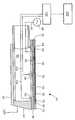
도 1 에 나타낸 플라즈마 반응로는, 정전기적으로 기판 (13) 을 클램핑하고 기판에 RF 바이어스 인가하는 정전기 척 (34) 을 가지는 기판 지지대 (12) 를 포함하는 반응 챔버 (10) 를 포함한다. 예를 들어, 기판 (13) 은 반도체 웨이퍼일 수 있다. 포커스 링 (14) 은 기판 (13) 상부의 플라즈마를 향상시킨다. 반응 챔버에서 플라즈마를 생성하기 위해 프로세스 가스에 에너지를 공급하는 에너지 소스가 반응 챔버 (10) 의 최상부에 배치된다. 예를 들어, 에너지 소스는 RF 소스 (19) 에 의해 전력공급되는 안테나일 수 있다. 반응 챔버 (10) 는 챔버의 내부를 원하는 압력으로 유지하기 위한 진공 펌프 장치를 포함한다.The plasma reaction reactor shown in FIG. 1 includes a
안테나 (18) 와 프로세싱 챔버 (10) 의 내부 사이에 유전체 윈도우 (20) 가 배치된다. 가스 분배 플레이트 (22) 가 원도우 (20) 하단에 존재하고, 개구부들을 포함하며, 이 개구부를 통해 프로세스 가스가 가스 서플라이 (23) 로부터 반응 챔버 (10) 로 전달된다.A
동작에서, 기판 (13) 은 기판 홀더 (12) 의 노출된 상단면 상에 배치되고, 정전기 척 (34) 에 의해 정전기적으로 클램핑된다. 바람직하게는, 열전도 가스가 기판 홀더 (12) 의 상단면과 기판 (13) 사이에 유입되어 기판 (13) 과 상단면 사이의 열전도를 향상시킨다. 프로세스 가스가 반응 챔버 (10) 로 공급된다. 안테나 (18) 에 RF 전력을 공급함으로써 반응 챔버 (10) 에서 플라즈마가 생성된다.In operation, the
도 2 는 기판 지지대 (40) 의 바람직한 실시형태를 나타낸다. 예를 들어, 기판 지지대 (40) 는 반응 챔버 (10) 에 이용될 수 있다. 기판 지지대 (40) 는 바닥 커버 (42), 커버 (42) 상의 베이스 (44), 베이스 (44) 상단에 위치하고 내부 공간 (56) 을 포위하는 세라믹 부재 (46), 세라믹 부재 (46) 상단에 위치하는 저질량 열전도 부재 (48), 및 열전도 부재 (48) 상단에 위치하는 정전기 척 (50) 을 포함한다. RF 전력 소스 (49) 는 전기적 도전체 (51) 를 통해 열전도 부재 (48) 에 전기적으로 접속되어 RF 바이어스를 제공한다. 에지 링 (52) 이 세라믹 부재 (46) 상단에 위치하고 열전도 부재 (48) 및 정전기 척 (50) 을 포위한 다. 에지 링 (52) 은 석영, SiC, 등으로 조성될 수 있다. 기판 (70) 은 정전기 척 (50) 상에 지지되는 것으로 나타나 있다.2 shows a preferred embodiment of the
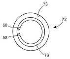
기판 지지대 (40) 는 열전도 부재 (48) 에 제공된 하나 이상의 플로우 경로와 유통하는 인렛 (inlet; 58) 및 아웃렛 (outlet; 60) 을 포함한다. 인렛 (58) 및 아웃렛 (60) 은 각각 서플라이 라인 (102) 및 리턴 라인 (104) 을 통해 액체 소스 (100) 와 유통한다. 액체는 액체 소스 (100) 로부터 서플라이 라인 (102) 을 통해, 열전도 부재 (48) 의 플로우 경로 안으로 인렛 (58) 을 통해, 플로우 경로를 통해, 그리고 아웃릿 (60) 및 리턴 라인 (104) 을 통해 액체 소스 (100) 로 리턴된다. 바람직하게는, 액체 소스 (100) 의 동작은, 액체 소스 (100) 와 제어 통신중인 제어기 (200) 에 의해 제어된다.The
베이스 (44) 는 알루미늄, 알루미늄 합금 등과 같은 금속으로 조성된다. 베이스 (44) 는 전기적으로 접지된다.The base 44 is made of metal such as aluminum, aluminum alloy, or the like. Base 44 is electrically grounded.
도 2 에 나타낸 실시형태에서, 세라믹 부재 (46) 는 베이스 (44) 에 고정된다. 예를 들어, 세라믹 부재 (46) 를 베이스 (44) 에 고정 (fasten) 하기 위해 볼트, 나사 등과 같은 메이팅 패스너 (mating fastener) 를 수납하기 위해 금속 삽입물 등이 세라믹 부재 (46) 에 삽입될 수 있다. 세라믹 부재 (46) 는 적당한 물질로 조성되고, 그리고 또한 세라믹 부재 (46) 의 바닥면 (62) 에 작용하는 압력 (일반적으로 대기압) 을 카운터발란스하기에 충분한 강성을 가지도록 구성된다. 바람직하게는, 세라믹 부재 (46) 는 플라즈마 프로세싱 동안 왜곡 (deflection) 을 견딜 수 있는 충분히 높은 모듈러스 (modulus) (예를 들어, 적어도 15 Mpsi) 를 가 진다. 세라믹 부재 (46) 의 왜곡을 최소화함으로써, 세라믹 부재 (46), 및 상단에 위치하는 열전도 부재 (48) 및 정전기 척 (50) 의 공간적인 (dimensional) 안정성이 플라즈마 프로세싱 동안 유지된다. 예를 들어, 세라믹 부재 (46) 는 가장 얇은 부분에서 약 1 내지 4 ㎜ 의 두께를 가질 수 있다. 프로세싱 동안, 베이스 (44) 는 열전도 부재 (48) 보다 온도가 높거나 낮을 수도 있다. 바람직하게는, 세라믹 부재 (46) 는 베이스 (44) 로부터 열적으로 격리되기에 충분할 만큼 낮은 열전도성을 가진다. 또한, 세라믹 부재 (46) 는 RF 구동 열전도 부재 (48) 에 대해 접지로부터의 RF 절연을 제공한다. 세라믹 부재 (46) 는 알루미늄 (Al2O3) 또는 다른 적당한 물질로 조성될 수 있다.In the embodiment shown in FIG. 2, the
바람직한 실시형태에서, 세라믹 부재 (46) 는 주변의 프린지 (64) 에 의해 포위된 중앙이 오목한 (recessed) 표면 (63) 을 가진다. 오목한 표면 (63) 은 세라믹 부재 (46) 가 형성된 후, 밀링 등과 같은 기계가공 프로세스에 의해 형성될 수 있다. 다른 방법으로는, 오목한 표면 (63) 은 예를 들어 몰딩 또는 캐스팅과 같은 세라믹 부재 (46) 를 형성하기 위해 이용되는 프로세스에 의해 형성될 수 있다. 바람직하게는, 열전도 부재 (48) 는 프린지 (64) 와 같은 높이로 오목한 표면 (63) 에 배치된다.In a preferred embodiment, the
바람직하게는, 열전도 부재 (48) 는 세라믹 부재 (46) 의 오목한 표면 (63) 에 접착적으로 결합된다. 바람직하게는, 세라믹 부재 (46) 와 열전도 부재 (48) 사이에 도포되는 접착제는 열전도 부재 (48) 를 세라믹 부재 (46) 로부터 열 적으로 절연시키도록 낮은 열전도성을 가진다. 또한 바람직하게는, 접착제는 반도체 기판의 플라즈마 프로세싱 동안 세라믹 부재 (46) 와 열전도 부재 (48) 사이에 생성되는 열 변형 (strain) 을 수용하기에 충분한 탄성을 가진다. 바람직하게는, 접착제는, 제너널 일렉트릭 (General Electic) 에서 생산하는 RTV 133 및 RTV 167 등의 실온-경화형 접착제와 같은 탄성중합체 물질이다.Preferably, the thermally
바람직하게는, 열전도 부재 (48) 는 오목한 표면 (63) 보다 더 작은 폭을 가져서 열전도 부재 (48) 의 주변 에지는 프린지 (64) 로부터 옆으로 (laterally) 이격된다. 예를 들어, 오목한 표면 (63) 은 원형일 수 있고, 열전도 부재 (48) 도 원형이고 오목한 표면 (63) 보다 더 작은 직경을 가질 수 있다 (도 3). 정전기 척 (50) 은 프린지 (64) 및 열전도 부재 (48) 상에 탑재된다. 예를 들어, 300 ㎜ 웨이퍼 프로세싱의 경우, 정전기 척 (50) 이 프린지 (64) 에 접촉하도록, 정전기 척 (50) 은 대략 오목한 표면 (63) 및 웨이퍼의 직경과 동일한 직경, 예를 들어 약 298 ㎜ 의 직경을 가질 수 있다. 열전도 부재 (48) 는 프린지로부터 이격되도록 약 298 ㎜ 보다 작은 직경을 가질 수 있다.Preferably, the thermally
도 4 에 나타낸 바와 같이, 열전도 부재 (48) 는 바람직하게는, 베이스 (72) 및 상단에 위치하는 커버 (74) 를 포함한다. 열전도 부재 (48) 는 구리, 구리 합금, 알루미늄, 알루미늄 합금 등과 같은 충분한 열전도 특성을 가지는 금속으로 조성될 수 있다. 베이스 (72) 및 커버 (74) 는 바람직하게는, 그 사이에 유체 씨일 (seal) 을 제공하도록 브레이징 (brazing) 등에 의해 함께 결합된다.As shown in FIG. 4, the heat
바람직하게는, 베이스 (72) 는 약 ¼ 인치 이하의 두께를 가지고, 더욱 바람 직하게는, 약 1/8 인치 이하의 두께를 가진다. 바람직하게는, 커버 (74) 는 1/16 인치 이하의 두께를 가진다. 바람직하게는, 기판 (72) 및 커버 (74) 는 약 ¼ 인치의 최대 결합 두께, 더욱 바람직하게는 약 ⅛ 인치의 최대 결합 두께를 가진다.Preferably,
베이스 (72) 는 하나 이상의 플로우 경로가 형성되는 최상부 표면 (73) 을 포함한다. 도 5 는 원형 플로우 경로 (76) 를 포함하는 베이스 (72) 의 바람직한 실시형태를 나타낸다. 액체가 인렛 (58) 및 서플라이 라인 (102) 을 경유해 플로우 경로 (76) 로 유입되고, 액체는 아웃렛 (60) 및 리턴 라인 (104) 을 경유해 액체 소스 (100) 로 리턴된다. 플로우 경로는 열전도 부재 (48) 의 온도 제어를 제공하기 위해 베이스 (72) 에서 다른 배열을 가질 수 있다. 예를 들어, 플로우 경로는 소용돌이, 지그재그, 또는 다른 패턴을 대체적으로 가질 수 있다.
베이스 (72) 의 플로우 경로는, 예를 들어 반원형, 원형, 직사각형, 정사각형, 다른 다각형 형상 등을 포함하는 다양한 단면 형상을 가질 수 있다. 플로우 경로를 통하는 액체의 원하는 체적 플로우 레이트 및 액체의 열전도 성능에 기초하여 플로우 경로의 원하는 체적을 제공하기 위해, 플로우 경로의 횡단하는 (transverse) 단면 영역이 선택될 수 있다. 바람직한 실시형태에서, 플로우 경로는 약 1/32 내지 3/32 인치의 폭 및 약 1/32 내지 1/16 인치의 깊이를 가진다.The flow path of the base 72 can have various cross-sectional shapes, including, for example, semicircular, circular, rectangular, square, other polygonal shapes, and the like. The transverse cross-sectional area of the flow path can be selected to provide the desired volume of the flow path based on the desired volume flow rate of the liquid through the flow path and the thermal conductivity performance of the liquid. In a preferred embodiment, the flow path has a width of about 1/32 to 3/32 inches and a depth of about 1/32 to 1/16 inches.
베이스 (72) 의 플로우 경로는 임의의 적합한 프로세스로 형성될 수 있다. 예를 들어, 플로우 경로는 베이스 (72) 가 형성된 후에 기계가공 프로세스에 의하는 것과 같이 최상부 표면 (73) 에 형성될 수 있다. 이와 다르게는, 플로우 경 로는 바디의 제조 동안, 캐스팅, 포징 (forging), 스탬핑 또는 다른 프로세스에 의하는 것과 같이 형성될 수 있다.The flow path of the base 72 can be formed in any suitable process. For example, a flow path can be formed on the
액체는 물 (예를 들어, 탈이온수), 에틸렌 글리콜, 실리콘 오일, 물/에틸렌 글리콜 혼합물 등일 수 있다. 액체의 냉각 성능은, 상이한 액체 및/또는 상이한 액체의 혼합물의 사용, 액체 플로우 레이트의 변화, 및/또는 플로우 경로로 유입되는 액체의 온도의 변화에 의해 제어될 수 있다. 바람직하게는, 액체의 온도는 액체 소스 (100) 에 의해 조정될 수 있다.The liquid may be water (eg deionized water), ethylene glycol, silicone oil, water / ethylene glycol mixture, and the like. The cooling performance of the liquid can be controlled by the use of different liquids and / or mixtures of different liquids, changes in the liquid flow rate, and / or changes in the temperature of the liquid entering the flow path. Preferably, the temperature of the liquid can be adjusted by the
도 2 를 참조하면, 정전기 척 (50) 은 유전체 물질에 샌드위치된 전기적으로 전도성의 전극 (또는 바이폴라 동작을 위한 한 쌍의 전극) 을 포함한다. 기판 (70) 을 클램핑하기 위해 전극이 제공된다. RF 바이어스는 정전기 척 (50) 을 통해 기판 (70) 에 용량성 결합된다. 바람직하게는, 열전도 부재 (48) 는 결합 균일성을 향상시키기 위해 평평한 상부 표면을 가진다. 유전체 물질은 알루미나 등과 같은 적당한 세라믹 물질일 수 있다. 도전성 전극은 텅스텐 등으로 조성될 수 있다. 예를 들어, 정전기 척 (50) 은 약 1㎜ 의 두께를 가질 수 있다. 정전기 척 (50) 은 그것의 주변 에지가 세라믹 물질 (46) 의 프린지 (64) 와 접촉하도록 두께를 가진다. 따라서, 열전도 부재 (48) 로의 직접적인 RF 경로는 존재하지 않으며, 이는 아크방전을 방지한다. 유전체 물질은 기판 (70) 을 지지하기 위한 정전기 척 (50) 의 노출된 표면을 형성한다. 바람직하게는, 노출된 표면은 웨이퍼의 형상의 기판 (70) 의 형상과 일치하도록 원형이다.Referring to FIG. 2,
도 6 에 나타낸 다른 바람직한 실시형태에서, 세라믹 부재 (146) 는 열전도 부재 (48) 가 배치되는 평탄면 (planar surface; 147) (즉, 오목하지 않은 표면) 을 가진다. 정전기 척 (50) 은 열전도 부재 (48) 의 상단에 위치한다. 웨이퍼 (70) 는 정전기 척 (50) 상에 배치되는 것으로 나타나 있다. 내부 링 (80) 은 표면 (147) 상에 배치되고, 열전도 부재 (48), 정전기 척 (50), 및 웨이퍼 (70) 를 포위한다. 에지 링 (52) 은 내부 링 (80) 을 포위한다. 바람직하게는, 내부링 (80) 은 세라믹 부재 (146) 와 동일한 재료 (예를 들어, 알루미나) 로 조성된다. 열전도 부재 (48) 는 내부 링 (80) 으로부터 공간 (82) 만큼 옆으로 이격되어 있다. 정전기 척 (50) 은 내부 링 (80) 에 접촉한다.In another preferred embodiment shown in FIG. 6, the
바람직하게는, 정전기 척 (50) 은, 탄성중합체 물질과 같은 적당한 접착 물질로 열전도 부재 (48) 에 부착된다. 바람직하게는, 접착제는, 정전기 척 (50) 과 하단에 위치하는 열전도 부재 (48) 사이의 충분한 열전도를 제공하기 위해 그것의 열전도성을 향상시키도록, 금속 충전제 (metallic filler) 와 같은 물질을 포함한다. 예를 들어, 접착제는 전도성을 향상시키도록 하나 이상의 금속 또는 금속 합금의 입자를 포함한다.Preferably,
전술한 바와 같이, (일반적으로 알루미늄으로 조성되는) 큰 금속제 콜드 플레이트는 1¼ 인치 이상의 두께 및 대응하는 큰 열식 질량을 가질 수 있다. 반대로, 열전도 부재 (48) 는 바람직하게는 이러한 큰 콜드 플레이트의 체적의 약 5 내지 10 % 와 동일한 체적을 가진다. 열전도 부재 (48) 의 상당히 감소된 체적으로 인해, 열전도 부재 (48) 의 온도를 주어진 양만큼 변화시키기 위해 차감되거나 가해질 필요가 있는 열량은 이러한 큰 콜드 플레이트에 비해 상당히 감소된다. 바람직하게는, 열전도 부재 (48) 는 약 0.25 ℃/초 내지 약 2 ℃/초의 레이트로 가열 및/또는 냉각될 수 있다. 이에 비해, 큰 열식 질량을 가지는 큰 콜드 플레이트는 약 1 ℃/분 이하에 불과한 온도 변화 레이트를 제공한다. 바람직하게는, 열전도 부재 (48) 는 플라즈마 프로세싱 동안 약 -20 ℃ 내지 80 ℃ 의 범위의 온도로 제어될 수 있다.As noted above, large metal cold plates (generally composed of aluminum) may have a thickness of at least 1¼ inch and a corresponding large thermal mass. In contrast, the thermally
또한, 열전도 부재 (48) 의 낮은 열식 질량으로 인해, 열전도 부재 (48) 를 원하는 온도로 가열 및/또는 냉각하기 위해 열전도 부재 (48) 로 공급될 필요가 있는 액체의 체적 플로우 레이트는, 큰 열식 질량을 가지는 큰 콜드 플레이트를 가열 및/또는 냉각하기 위해 필요한 액체 플로우 레이트에 비해 상당히 감소된다.Also, due to the low thermal mass of the thermally
기판 지지대 (40) 의 바람직한 실시형태는 액체 소스 (100), 열전도 가스 소스 (150; 도 6), 및 제어기 (200) 를 포함한다. 전술한 바와 같이, 액체 소스 (100; 도 2) 는 열전도 부재 (48) 의 플로우 경로에 액체를 공급한다. 액체 소스 (100) 는, 플로우 경로에 선택된 온도 및/또는 플로우 레이트로 액체를 공급하기 위해 열전기 냉각기 (예를 들어, 펠티에 (Peltier) 냉각기), 열 교환기 등을 포함할 수 있다. 액체 소스 (100) 는 적당한 펌프 배열을 포함할 수 있다. 바람직하게는, 액체가 액체 소스 (100) 로부터 흐르는 거리를 감소시키기 위해 냉각기 등은 열전도 부재 (48) 에 가깝게 배치됨으로써 가열 또는 냉각될 필요가 있는 플로우 경로의 액체 체적을 줄이고 또한 액체 소스의 응답 시간을 줄인다.Preferred embodiments of the
열전도 가스 소스는 열전도 가스 경로에 열전도 가스를 공급한다. 열전도 가스는 열전도 가스 경로를 통해, 정전기 척 (50) 의 노출된 표면으로 흐르고, 노출된 표면에 형성된 개구부 및/또는 채널 (미도시) 을 통해, 노출된 표면과 기판 (70; 도 6) 의 백사이드 사이의 인터페이스 (85) 로 가스가 분배된다. 기판 지지대의 노출된 표면의 구역 (zone) 냉각을 제공하는 적합한 열전도 가스 공급 시스템은, 참조 (reference) 에 의해 그 전체로 여기에 포함되는, 공동으로 양도된 미국 특허 제 5,609,720 호에 개시되어 있다. 열전도 가스는, 플라즈마 프로세싱 동안 기판으로부터 열을 충분히 전도할 수 있는 열전도 성능을 가지는 임의의 가스일 수 있다. 예를 들어, 열전도 가스는 헬륨 등일 수 있다.The thermally conductive gas source supplies the thermally conductive gas to the thermally conductive gas path. The thermally conductive gas flows through the thermally conductive gas path to the exposed surface of the
제어기 (200) 는 바람직하게는, 플로우 경로로 공급되는 액체의 파라미터를 선택적으로 변화시키도록 액체 소스의 동작을 제어하고, 또한 열전도 가스 경로로 공급되는 열전도 가스의 파라미터를 선택적으로 변화시키도록 열전도 가스 소스 (150) 의 동작을 제어한다. 제어기 (200) 는 바람직하게는, 액체 소스에 의해 플로우 경로로 공급되는 액체의 온도 및/또는 플로우 레이트를 제어하도록 액체 소스 (100) 의 동작을 제어하고, 노출된 표면에서 원하는 온도를 달성하기 위해 인터페이스 부분으로 공급되는 열전도 가스의 플로우 레이트 및/또는 압력을 제어하도록 열전도 가스 소스 (150) 를 제어한다.The
제어기 (200) 는 바람직하게는, 기판 지지대 (40) 및/또는 기판 (예를 들어, 백사이드) 의 하나 이상의 선택된 위치에서의 온도를 측정하기 위해 기판 지지대 (40) 에 배치된 하나 이상의 온도 센서로부터 입력 신호를 수신한다. 예를 들어, 온도 센서는 정전기 척 (50) 의 노출된 표면에 가까운 위치에서의 온도를 측정하도록 배치될 수 있다. 바람직하게는, 액체 소스 (100) 의 동작의 피드백 제 어 및 열전도 가스 소스 (150) 의 동작의 제어를 가능하게 하기 위한 실시간 온도 측정을 제공한다. 제어기 (200) 는 수동 동작되거나 액체 소스 (100) 및 열전도 가스 소스 (150) 의 동작을 자동적으로 제어하도록 프로그래밍될 수 있다.The
기판 지지대 (40) 는, 플라즈마 에칭, 물리적 기상증착, 화학적 기상증착 (CVD), 이온 주입, 및/또는 레지스트 제거를 포함하는 다양한 플라즈마 프로세싱 동작이 수행되는 플라즈마 프로세싱 장치에 이용될 수 있다. 플라즈마 프로세싱 동작은 반도체, 유전체 및 금속제 물질을 포함하는 다양한 기판 물질에 대해 수행될 수 있다.The
기판 지지대 (40) 는 다양한 진공 반도체 프로세스에 유용한 다이나믹하고, 근사 온도 제어를 제공할 수 있다. 예를 들어, 이 특성들은 게이트 및 얕은 트렌치 절연 (shallow trench isolation; STI) 에칭 프로세스에서 정확하고 단계-변환가능한 (step-changeable) 온도 제어에 유용하다. 이와 다르게는, 예를 들어, 기판 지지대 (40) 온도는, 에칭 동안, 기판에서 테이퍼링 사이드월 (tapering sidewall) 을 형성하도록 (예를 들어, 선형적으로) 램핑 (ramping) 될 수 있다. 기판 온도를 신속하게 변화시키는 성능은, 기판으로부터 신속하게 열이 제거되지 않으면 이용되는 고전력 밀도가 신속한 웨이퍼 과온 (over-temperature) 상태 발생을 유발할 수 있는 유전체 물질 에칭 프로세스와 같은 다양한 프로세스에서 유용하다.
발명을 특정 실시형태들을 참조하여 상세하게 설명했지만, 첨부된 청구범위의 범위를 벗어나지 않고 다양한 변경 및 변형이 만들어질 수 있고, 균등물들이 채 택될 수 있음이 당업자에게 명확하다.Although the invention has been described in detail with reference to specific embodiments, it will be apparent to those skilled in the art that various changes and modifications may be made and equivalents may be employed without departing from the scope of the appended claims.
Claims (31)
Translated fromKoreanApplications Claiming Priority (2)
| Application Number | Priority Date | Filing Date | Title |
|---|---|---|---|
| US10/608,091US7993460B2 (en) | 2003-06-30 | 2003-06-30 | Substrate support having dynamic temperature control |
| US10/608,091 | 2003-06-30 |
Related Child Applications (1)
| Application Number | Title | Priority Date | Filing Date |
|---|---|---|---|
| KR1020127014042ADivisionKR20120066683A (en) | 2003-06-30 | 2004-06-28 | Substrate support having dynamic temperature control |
Publications (1)
| Publication Number | Publication Date |
|---|---|
| KR20060025586Atrue KR20060025586A (en) | 2006-03-21 |
Family
ID=33540476
Family Applications (3)
| Application Number | Title | Priority Date | Filing Date |
|---|---|---|---|
| KR1020137007852AExpired - Fee RelatedKR101476566B1 (en) | 2003-06-30 | 2004-06-28 | Substrate support having dynamic temperature control |
| KR1020057025443ACeasedKR20060025586A (en) | 2003-06-30 | 2004-06-28 | Substrate Support with Dynamic Temperature Control |
| KR1020127014042ACeasedKR20120066683A (en) | 2003-06-30 | 2004-06-28 | Substrate support having dynamic temperature control |
Family Applications Before (1)
| Application Number | Title | Priority Date | Filing Date |
|---|---|---|---|
| KR1020137007852AExpired - Fee RelatedKR101476566B1 (en) | 2003-06-30 | 2004-06-28 | Substrate support having dynamic temperature control |
Family Applications After (1)
| Application Number | Title | Priority Date | Filing Date |
|---|---|---|---|
| KR1020127014042ACeasedKR20120066683A (en) | 2003-06-30 | 2004-06-28 | Substrate support having dynamic temperature control |
Country Status (8)
| Country | Link |
|---|---|
| US (2) | US7993460B2 (en) |
| EP (1) | EP1644962A4 (en) |
| JP (2) | JP5053632B2 (en) |
| KR (3) | KR101476566B1 (en) |
| CN (1) | CN100440422C (en) |
| MY (1) | MY151676A (en) |
| TW (1) | TWI338931B (en) |
| WO (1) | WO2005006400A2 (en) |
Families Citing this family (78)
| Publication number | Priority date | Publication date | Assignee | Title |
|---|---|---|---|---|
| WO2004095529A2 (en)* | 2003-03-21 | 2004-11-04 | Tokyo Electron Limited | Method and apparatus for reducing substrate backside deposition during processing |
| US7993460B2 (en) | 2003-06-30 | 2011-08-09 | Lam Research Corporation | Substrate support having dynamic temperature control |
| US6976782B1 (en)* | 2003-11-24 | 2005-12-20 | Lam Research Corporation | Methods and apparatus for in situ substrate temperature monitoring |
| US7544251B2 (en)* | 2004-10-07 | 2009-06-09 | Applied Materials, Inc. | Method and apparatus for controlling temperature of a substrate |
| US7648914B2 (en) | 2004-10-07 | 2010-01-19 | Applied Materials, Inc. | Method for etching having a controlled distribution of process results |
| US7436645B2 (en) | 2004-10-07 | 2008-10-14 | Applied Materials, Inc. | Method and apparatus for controlling temperature of a substrate |
| KR100899244B1 (en)* | 2005-03-03 | 2009-05-27 | 어플라이드 머티어리얼스, 인코포레이티드 | Method for etching having a controlled distribution of process results |
| JP4647401B2 (en) | 2005-06-06 | 2011-03-09 | 東京エレクトロン株式会社 | Substrate holder, substrate temperature control apparatus, and substrate temperature control method |
| US8226769B2 (en) | 2006-04-27 | 2012-07-24 | Applied Materials, Inc. | Substrate support with electrostatic chuck having dual temperature zones |
| US9275887B2 (en) | 2006-07-20 | 2016-03-01 | Applied Materials, Inc. | Substrate processing with rapid temperature gradient control |
| US7528392B2 (en) | 2006-11-27 | 2009-05-05 | Varian Semiconductor Equipment Associates, Inc. | Techniques for low-temperature ion implantation |
| JP4450245B2 (en)* | 2007-06-07 | 2010-04-14 | 株式会社デンソー | Manufacturing method of semiconductor device |
| TWI508129B (en)* | 2007-10-31 | 2015-11-11 | Lam Res Corp | Temperature control module using gas pressure to control thermal conductance between liquid coolant and component body |
| CN101903996B (en)* | 2007-12-21 | 2013-04-03 | 应用材料公司 | Method and apparatus for controlling temperature of a substrate |
| US8352015B2 (en)* | 2008-05-27 | 2013-01-08 | Kyma Medical Technologies, Ltd. | Location tracking of a metallic object in a living body using a radar detector and guiding an ultrasound probe to direct ultrasound waves at the location |
| US9265438B2 (en) | 2008-05-27 | 2016-02-23 | Kyma Medical Technologies Ltd. | Locating features in the heart using radio frequency imaging |
| US8989837B2 (en)* | 2009-12-01 | 2015-03-24 | Kyma Medical Technologies Ltd. | Methods and systems for determining fluid content of tissue |
| US20100116788A1 (en)* | 2008-11-12 | 2010-05-13 | Lam Research Corporation | Substrate temperature control by using liquid controlled multizone substrate support |
| US20100144140A1 (en)* | 2008-12-10 | 2010-06-10 | Novellus Systems, Inc. | Methods for depositing tungsten films having low resistivity for gapfill applications |
| US8129270B1 (en) | 2008-12-10 | 2012-03-06 | Novellus Systems, Inc. | Method for depositing tungsten film having low resistivity, low roughness and high reflectivity |
| US9548228B2 (en) | 2009-08-04 | 2017-01-17 | Lam Research Corporation | Void free tungsten fill in different sized features |
| US9034768B2 (en)* | 2010-07-09 | 2015-05-19 | Novellus Systems, Inc. | Depositing tungsten into high aspect ratio features |
| US8124531B2 (en) | 2009-08-04 | 2012-02-28 | Novellus Systems, Inc. | Depositing tungsten into high aspect ratio features |
| US10256142B2 (en) | 2009-08-04 | 2019-04-09 | Novellus Systems, Inc. | Tungsten feature fill with nucleation inhibition |
| US8410393B2 (en)* | 2010-05-24 | 2013-04-02 | Lam Research Corporation | Apparatus and method for temperature control of a semiconductor substrate support |
| US9220420B2 (en) | 2010-07-21 | 2015-12-29 | Kyma Medical Technologies Ltd. | Implantable dielectrometer |
| JP5781803B2 (en)* | 2011-03-30 | 2015-09-24 | 東京エレクトロン株式会社 | Temperature control method and plasma processing system |
| US8520360B2 (en) | 2011-07-19 | 2013-08-27 | Lam Research Corporation | Electrostatic chuck with wafer backside plasma assisted dechuck |
| US20130240144A1 (en)* | 2012-03-13 | 2013-09-19 | Applied Materials, Inc. | Fast response fluid temperature control system |
| TWI602283B (en) | 2012-03-27 | 2017-10-11 | 諾發系統有限公司 | Tungsten feature fill |
| US9132436B2 (en) | 2012-09-21 | 2015-09-15 | Applied Materials, Inc. | Chemical control features in wafer process equipment |
| US8970114B2 (en) | 2013-02-01 | 2015-03-03 | Lam Research Corporation | Temperature controlled window of a plasma processing chamber component |
| US9287147B2 (en) | 2013-03-14 | 2016-03-15 | Applied Materials, Inc. | Substrate support with advanced edge control provisions |
| US9082826B2 (en) | 2013-05-24 | 2015-07-14 | Lam Research Corporation | Methods and apparatuses for void-free tungsten fill in three-dimensional semiconductor features |
| JP6159172B2 (en)* | 2013-06-26 | 2017-07-05 | 東京エレクトロン株式会社 | Temperature control method and plasma processing apparatus |
| US9859145B2 (en) | 2013-07-17 | 2018-01-02 | Lam Research Corporation | Cooled pin lifter paddle for semiconductor substrate processing apparatus |
| US10680324B2 (en) | 2013-10-29 | 2020-06-09 | Zoll Medical Israel Ltd. | Antenna systems and devices and methods of manufacture thereof |
| US11013420B2 (en) | 2014-02-05 | 2021-05-25 | Zoll Medical Israel Ltd. | Systems, apparatuses and methods for determining blood pressure |
| US20150228514A1 (en)* | 2014-02-12 | 2015-08-13 | Axcelis Technologies, Inc. | Multi Fluid Cooling System for Large Temperature Range Chuck |
| US11259715B2 (en) | 2014-09-08 | 2022-03-01 | Zoll Medical Israel Ltd. | Monitoring and diagnostics systems and methods |
| US10548485B2 (en) | 2015-01-12 | 2020-02-04 | Zoll Medical Israel Ltd. | Systems, apparatuses and methods for radio frequency-based attachment sensing |
| US20160225652A1 (en) | 2015-02-03 | 2016-08-04 | Applied Materials, Inc. | Low temperature chuck for plasma processing systems |
| CN104835761A (en)* | 2015-04-27 | 2015-08-12 | 沈阳拓荆科技有限公司 | Temperature-controllable heating disc enabling peripheral outgassing |
| JP6655310B2 (en) | 2015-07-09 | 2020-02-26 | 株式会社日立ハイテクノロジーズ | Plasma processing equipment |
| US9741593B2 (en) | 2015-08-06 | 2017-08-22 | Applied Materials, Inc. | Thermal management systems and methods for wafer processing systems |
| TWI808334B (en)* | 2015-08-06 | 2023-07-11 | 美商應用材料股份有限公司 | Workpiece holder |
| US9972504B2 (en) | 2015-08-07 | 2018-05-15 | Lam Research Corporation | Atomic layer etching of tungsten for enhanced tungsten deposition fill |
| US9978610B2 (en) | 2015-08-21 | 2018-05-22 | Lam Research Corporation | Pulsing RF power in etch process to enhance tungsten gapfill performance |
| US10504700B2 (en) | 2015-08-27 | 2019-12-10 | Applied Materials, Inc. | Plasma etching systems and methods with secondary plasma injection |
| CN106637132B (en)* | 2015-10-29 | 2020-01-10 | 沈阳拓荆科技有限公司 | Wafer reaction table with circulating medium for automatic temperature control and heat conduction gas for temperature conduction |
| JP6697089B2 (en)* | 2016-03-18 | 2020-05-20 | エーシーエム リサーチ (シャンハイ) インコーポレーテッド | Substrate heat treatment equipment |
| US10648080B2 (en)* | 2016-05-06 | 2020-05-12 | Applied Materials, Inc. | Full-area counter-flow heat exchange substrate support |
| US10504754B2 (en) | 2016-05-19 | 2019-12-10 | Applied Materials, Inc. | Systems and methods for improved semiconductor etching and component protection |
| US9865484B1 (en) | 2016-06-29 | 2018-01-09 | Applied Materials, Inc. | Selective etch using material modification and RF pulsing |
| US10566211B2 (en) | 2016-08-30 | 2020-02-18 | Lam Research Corporation | Continuous and pulsed RF plasma for etching metals |
| US10725485B2 (en)* | 2016-12-15 | 2020-07-28 | Lam Research Corporation | System and method for calculating substrate support temperature |
| US11276590B2 (en) | 2017-05-17 | 2022-03-15 | Applied Materials, Inc. | Multi-zone semiconductor substrate supports |
| JP7176860B6 (en) | 2017-05-17 | 2022-12-16 | アプライド マテリアルズ インコーポレイテッド | Semiconductor processing chamber to improve precursor flow |
| US11276559B2 (en) | 2017-05-17 | 2022-03-15 | Applied Materials, Inc. | Semiconductor processing chamber for multiple precursor flow |
| KR102439617B1 (en)* | 2017-06-27 | 2022-09-05 | 주식회사 미코세라믹스 | Bonding head and apparatus for bonding chips having the bonding head |
| US10199252B2 (en)* | 2017-06-30 | 2019-02-05 | Taiwan Semiconductor Manufacturing Company, Ltd. | Thermal pad for etch rate uniformity |
| US10297458B2 (en) | 2017-08-07 | 2019-05-21 | Applied Materials, Inc. | Process window widening using coated parts in plasma etch processes |
| US11020002B2 (en) | 2017-08-10 | 2021-06-01 | Zoll Medical Israel Ltd. | Systems, devices and methods for physiological monitoring of patients |
| US11328909B2 (en) | 2017-12-22 | 2022-05-10 | Applied Materials, Inc. | Chamber conditioning and removal processes |
| US11049755B2 (en) | 2018-09-14 | 2021-06-29 | Applied Materials, Inc. | Semiconductor substrate supports with embedded RF shield |
| US11062887B2 (en) | 2018-09-17 | 2021-07-13 | Applied Materials, Inc. | High temperature RF heater pedestals |
| US11682560B2 (en) | 2018-10-11 | 2023-06-20 | Applied Materials, Inc. | Systems and methods for hafnium-containing film removal |
| US10548239B1 (en)* | 2018-10-23 | 2020-01-28 | Google Llc | Cooling electronic devices in a data center |
| US11121002B2 (en) | 2018-10-24 | 2021-09-14 | Applied Materials, Inc. | Systems and methods for etching metals and metal derivatives |
| US11437242B2 (en) | 2018-11-27 | 2022-09-06 | Applied Materials, Inc. | Selective removal of silicon-containing materials |
| US12420314B2 (en)* | 2019-10-18 | 2025-09-23 | Taiwan Semiconductor Manufacturing Co., Ltd. | Semiconductor cleaning apparatus and method |
| CN112786422B (en)* | 2019-11-08 | 2024-03-12 | 中微半导体设备(上海)股份有限公司 | Focusing ring, plasma processor and method |
| CN111276430B (en)* | 2020-01-20 | 2023-02-14 | 北京北方华创微电子装备有限公司 | Temperature control device in semiconductor equipment and semiconductor equipment |
| CN111979530B (en)* | 2020-08-28 | 2022-10-18 | 湖南红太阳光电科技有限公司 | Heating system and heating control method of PECVD (plasma enhanced chemical vapor deposition) equipment and PECVD equipment |
| KR102572570B1 (en)* | 2021-07-02 | 2023-08-29 | 광운대학교 산학협력단 | Substrate processing apparatus and temperature control method using multi-zone heat transfer structure |
| KR102721404B1 (en)* | 2022-05-19 | 2024-10-25 | 세메스 주식회사 | Substrate supporting apparatus and substrate processing apparatus including the same |
| TWI871537B (en)* | 2022-10-20 | 2025-02-01 | 張寶杰 | Planar external cooling device for wafer chamber, wafer chamber system and cooling method thereof |
| CN119314913A (en)* | 2024-12-17 | 2025-01-14 | 青岛四方思锐智能技术有限公司 | A method, system, device and storage medium for cooling a wafer boat box |
Family Cites Families (62)
| Publication number | Priority date | Publication date | Assignee | Title |
|---|---|---|---|---|
| JPS6060060A (en)* | 1983-09-12 | 1985-04-06 | 株式会社日立製作所 | Switchgear for door of railway rolling stock |
| US5225663A (en)* | 1988-06-15 | 1993-07-06 | Tel Kyushu Limited | Heat process device |
| JPH03190125A (en) | 1989-12-19 | 1991-08-20 | Fujitsu Ltd | Dry etching device |
| US5221403A (en)* | 1990-07-20 | 1993-06-22 | Tokyo Electron Limited | Support table for plate-like body and processing apparatus using the table |
| US5192849A (en)* | 1990-08-10 | 1993-03-09 | Texas Instruments Incorporated | Multipurpose low-thermal-mass chuck for semiconductor processing equipment |
| JPH05226292A (en) | 1992-02-13 | 1993-09-03 | Tokyo Electron Yamanashi Kk | Starting method for plasma-processing |
| KR0164618B1 (en)* | 1992-02-13 | 1999-02-01 | 이노우에 쥰이치 | Plasma process method using an electrostatic chuck |
| KR100238629B1 (en)* | 1992-12-17 | 2000-01-15 | 히가시 데쓰로 | Stage having eletrostatic chuck and plasma processing apparatus using same |
| US6544379B2 (en)* | 1993-09-16 | 2003-04-08 | Hitachi, Ltd. | Method of holding substrate and substrate holding system |
| TW277139B (en)* | 1993-09-16 | 1996-06-01 | Hitachi Seisakusyo Kk | |
| US5900103A (en)* | 1994-04-20 | 1999-05-04 | Tokyo Electron Limited | Plasma treatment method and apparatus |
| US5548470A (en)* | 1994-07-19 | 1996-08-20 | International Business Machines Corporation | Characterization, modeling, and design of an electrostatic chuck with improved wafer temperature uniformity |
| US5671116A (en)* | 1995-03-10 | 1997-09-23 | Lam Research Corporation | Multilayered electrostatic chuck and method of manufacture thereof |
| US5609720A (en)* | 1995-09-29 | 1997-03-11 | Lam Research Corporation | Thermal control of semiconductor wafer during reactive ion etching |
| US6231776B1 (en)* | 1995-12-04 | 2001-05-15 | Daniel L. Flamm | Multi-temperature processing |
| US6108189A (en)* | 1996-04-26 | 2000-08-22 | Applied Materials, Inc. | Electrostatic chuck having improved gas conduits |
| JP3360265B2 (en)* | 1996-04-26 | 2002-12-24 | 東京エレクトロン株式会社 | Plasma processing method and plasma processing apparatus |
| JPH1074600A (en)* | 1996-05-02 | 1998-03-17 | Tokyo Electron Ltd | Plasma processing equipment |
| EP0805475B1 (en) | 1996-05-02 | 2003-02-19 | Tokyo Electron Limited | Plasma processing apparatus |
| US6046439A (en)* | 1996-06-17 | 2000-04-04 | Mattson Technology, Inc. | System and method for thermal processing of a semiconductor substrate |
| US6170428B1 (en)* | 1996-07-15 | 2001-01-09 | Applied Materials, Inc. | Symmetric tunable inductively coupled HDP-CVD reactor |
| US5849076A (en)* | 1996-07-26 | 1998-12-15 | Memc Electronic Materials, Inc. | Cooling system and method for epitaxial barrel reactor |
| TW334609B (en)* | 1996-09-19 | 1998-06-21 | Hitachi Ltd | Electrostatic chuck, method and device for processing sanyle use the same |
| US5835334A (en)* | 1996-09-30 | 1998-11-10 | Lam Research | Variable high temperature chuck for high density plasma chemical vapor deposition |
| KR100430189B1 (en)* | 1996-10-11 | 2004-05-03 | 동경 엘렉트론 주식회사 | Plasma etching method |
| JPH10220909A (en)* | 1996-12-03 | 1998-08-21 | Komatsu Ltd | Fluid temperature control device |
| JPH10284360A (en)* | 1997-04-02 | 1998-10-23 | Hitachi Ltd | Substrate temperature control device and method |
| US6077357A (en)* | 1997-05-29 | 2000-06-20 | Applied Materials, Inc. | Orientless wafer processing on an electrostatic chuck |
| US6189483B1 (en)* | 1997-05-29 | 2001-02-20 | Applied Materials, Inc. | Process kit |
| US6083344A (en)* | 1997-05-29 | 2000-07-04 | Applied Materials, Inc. | Multi-zone RF inductively coupled source configuration |
| JPH1140654A (en) | 1997-07-17 | 1999-02-12 | Kokusai Electric Co Ltd | Substrate holding structure |
| US6007635A (en)* | 1997-11-26 | 1999-12-28 | Micro C Technologies, Inc. | Platform for supporting a semiconductor substrate and method of supporting a substrate during rapid high temperature processing |
| US6138745A (en)* | 1997-09-26 | 2000-10-31 | Cvc Products, Inc. | Two-stage sealing system for thermally conductive chuck |
| US5983644A (en)* | 1997-09-29 | 1999-11-16 | Applied Materials, Inc. | Integrated bake and chill plate |
| JP3980187B2 (en)* | 1998-07-24 | 2007-09-26 | 日本碍子株式会社 | Semiconductor holding device, its manufacturing method and its use |
| US6280584B1 (en)* | 1998-07-29 | 2001-08-28 | Applied Materials, Inc. | Compliant bond structure for joining ceramic to metal |
| KR100317829B1 (en)* | 1999-03-05 | 2001-12-22 | 윤종용 | Thermoelectric-cooling temperature control apparatus for semiconductor manufacturing process facilities |
| US6635580B1 (en)* | 1999-04-01 | 2003-10-21 | Taiwan Semiconductor Manufacturing Co. Ltd. | Apparatus and method for controlling wafer temperature in a plasma etcher |
| US6184504B1 (en)* | 1999-04-13 | 2001-02-06 | Silicon Thermal, Inc. | Temperature control system for electronic devices |
| US6179921B1 (en)* | 1999-04-19 | 2001-01-30 | Applied Materials, Inc. | Backside gas delivery system for a semiconductor wafer processing system |
| US6490146B2 (en)* | 1999-05-07 | 2002-12-03 | Applied Materials Inc. | Electrostatic chuck bonded to base with a bond layer and method |
| US6310755B1 (en)* | 1999-05-07 | 2001-10-30 | Applied Materials, Inc. | Electrostatic chuck having gas cavity and method |
| US6461801B1 (en)* | 1999-05-27 | 2002-10-08 | Matrix Integrated Systems, Inc. | Rapid heating and cooling of workpiece chucks |
| JP2001102435A (en)* | 1999-07-28 | 2001-04-13 | Tokyo Electron Ltd | Mounting table structure and treating apparatus |
| US6474986B2 (en)* | 1999-08-11 | 2002-11-05 | Tokyo Electron Limited | Hot plate cooling method and heat processing apparatus |
| US6451157B1 (en)* | 1999-09-23 | 2002-09-17 | Lam Research Corporation | Gas distribution apparatus for semiconductor processing |
| US6377437B1 (en)* | 1999-12-22 | 2002-04-23 | Lam Research Corporation | High temperature electrostatic chuck |
| JP3921913B2 (en) | 2000-03-13 | 2007-05-30 | 株式会社日立製作所 | Wafer processing apparatus and wafer manufacturing method |
| JP2001267403A (en) | 2000-03-21 | 2001-09-28 | Nhk Spring Co Ltd | Semiconductor wafer heating / cooling device |
| JP3448737B2 (en)* | 2000-05-25 | 2003-09-22 | 住友重機械工業株式会社 | Wafer chuck cooling plate and wafer chuck |
| KR20010111058A (en)* | 2000-06-09 | 2001-12-15 | 조셉 제이. 스위니 | Full area temperature controlled electrostatic chuck and method of fabricating same |
| WO2002017384A1 (en) | 2000-08-23 | 2002-02-28 | Applied Materials, Inc. | Electrostatic chuck temperature control method and system |
| JP3920015B2 (en)* | 2000-09-14 | 2007-05-30 | 東京エレクトロン株式会社 | Si substrate processing method |
| US6800173B2 (en)* | 2000-12-15 | 2004-10-05 | Novellus Systems, Inc. | Variable gas conductance control for a process chamber |
| JP4493863B2 (en)* | 2001-01-25 | 2010-06-30 | 東京エレクトロン株式会社 | Plasma processing apparatus, cleaning method thereof, and electrostatic chuck static elimination method |
| JP4593007B2 (en)* | 2001-05-23 | 2010-12-08 | 東京エレクトロン株式会社 | Mounting device |
| US6529686B2 (en)* | 2001-06-06 | 2003-03-04 | Fsi International, Inc. | Heating member for combination heating and chilling apparatus, and methods |
| JP3971603B2 (en)* | 2001-12-04 | 2007-09-05 | キヤノンアネルバ株式会社 | Insulating film etching apparatus and insulating film etching method |
| JP4493251B2 (en)* | 2001-12-04 | 2010-06-30 | Toto株式会社 | Electrostatic chuck module and substrate processing apparatus |
| US20070051471A1 (en)* | 2002-10-04 | 2007-03-08 | Applied Materials, Inc. | Methods and apparatus for stripping |
| US20040163601A1 (en)* | 2003-02-26 | 2004-08-26 | Masanori Kadotani | Plasma processing apparatus |
| US7993460B2 (en) | 2003-06-30 | 2011-08-09 | Lam Research Corporation | Substrate support having dynamic temperature control |
- 2003
- 2003-06-30USUS10/608,091patent/US7993460B2/enactiveActive
- 2004
- 2004-06-28JPJP2006517743Apatent/JP5053632B2/ennot_activeExpired - Fee Related
- 2004-06-28KRKR1020137007852Apatent/KR101476566B1/ennot_activeExpired - Fee Related
- 2004-06-28CNCNB2004800216848Apatent/CN100440422C/ennot_activeExpired - Fee Related
- 2004-06-28WOPCT/US2004/020749patent/WO2005006400A2/enactiveApplication Filing
- 2004-06-28EPEP04777208Apatent/EP1644962A4/ennot_activeWithdrawn
- 2004-06-28KRKR1020057025443Apatent/KR20060025586A/ennot_activeCeased
- 2004-06-28KRKR1020127014042Apatent/KR20120066683A/ennot_activeCeased
- 2004-06-29MYMYPI20042581patent/MY151676A/enunknown
- 2004-06-29TWTW093119132Apatent/TWI338931B/ennot_activeIP Right Cessation
- 2011
- 2011-06-24USUS13/168,134patent/US8747559B2/ennot_activeExpired - Fee Related
- 2011-11-28JPJP2011259478Apatent/JP2012099825A/enactivePending
Also Published As
| Publication number | Publication date |
|---|---|
| WO2005006400A2 (en) | 2005-01-20 |
| CN1849697A (en) | 2006-10-18 |
| KR20120066683A (en) | 2012-06-22 |
| US20040261721A1 (en) | 2004-12-30 |
| US8747559B2 (en) | 2014-06-10 |
| KR20130049819A (en) | 2013-05-14 |
| JP2007529102A (en) | 2007-10-18 |
| JP5053632B2 (en) | 2012-10-17 |
| TW200507158A (en) | 2005-02-16 |
| US7993460B2 (en) | 2011-08-09 |
| WO2005006400A3 (en) | 2006-04-13 |
| JP2012099825A (en) | 2012-05-24 |
| CN100440422C (en) | 2008-12-03 |
| US20110262315A1 (en) | 2011-10-27 |
| KR101476566B1 (en) | 2014-12-24 |
| EP1644962A4 (en) | 2010-11-17 |
| MY151676A (en) | 2014-06-30 |
| EP1644962A2 (en) | 2006-04-12 |
| TWI338931B (en) | 2011-03-11 |
Similar Documents
| Publication | Publication Date | Title |
|---|---|---|
| KR101476566B1 (en) | Substrate support having dynamic temperature control | |
| JP5006200B2 (en) | Heat transfer system for improving semiconductor processing uniformity. | |
| KR100733897B1 (en) | Uniform Temperature Plasma Reaction Chamber Components | |
| KR101364319B1 (en) | Electrostatic chuck with radial temperature control | |
| US7846254B2 (en) | Heat transfer assembly | |
| US8921740B2 (en) | Method and apparatus for controlling the spatial temperature distribution across the surface of a workpiece support | |
| US8216486B2 (en) | Temperature control module using gas pressure to control thermal conductance between liquid coolant and component body | |
| KR102151001B1 (en) | High temperature electrostatic chuck with real-time heat zone regulating capability | |
| KR100815539B1 (en) | Method and apparatus for controlling temperature of a substrate | |
| US6302966B1 (en) | Temperature control system for plasma processing apparatus | |
| US20020007795A1 (en) | Temperature control system for plasma processing apparatus | |
| JP2008522446A (en) | Method and apparatus for controlling spatial temperature distribution | |
| KR20100138580A (en) | Plasma dry etching apparatus having cold coupling means for raising and lowering the outermost temperature of the wafer depending on the material film to be etched and the gas to be used. | |
| US20030089457A1 (en) | Apparatus for controlling a thermal conductivity profile for a pedestal in a semiconductor wafer processing chamber | |
| KR20210004056A (en) | Shower head unit and system for treating substrate with the shower head unit |
Legal Events
| Date | Code | Title | Description |
|---|---|---|---|
| PA0105 | International application | Patent event date:20051230 Patent event code:PA01051R01D Comment text:International Patent Application | |
| PG1501 | Laying open of application | ||
| A201 | Request for examination | ||
| PA0201 | Request for examination | Patent event code:PA02012R01D Patent event date:20090626 Comment text:Request for Examination of Application | |
| E902 | Notification of reason for refusal | ||
| PE0902 | Notice of grounds for rejection | Comment text:Notification of reason for refusal Patent event date:20110216 Patent event code:PE09021S01D | |
| E601 | Decision to refuse application | ||
| PE0601 | Decision on rejection of patent | Patent event date:20120328 Comment text:Decision to Refuse Application Patent event code:PE06012S01D Patent event date:20110825 Comment text:Notification of reason for refusal Patent event code:PE06011S01I Patent event date:20110216 Comment text:Notification of reason for refusal Patent event code:PE06011S01I | |
| J201 | Request for trial against refusal decision | ||
| PJ0201 | Trial against decision of rejection | Patent event date:20120430 Comment text:Request for Trial against Decision on Refusal Patent event code:PJ02012R01D Patent event date:20120328 Comment text:Decision to Refuse Application Patent event code:PJ02011S01I Appeal kind category:Appeal against decision to decline refusal Decision date:20130917 Appeal identifier:2012101004129 Request date:20120430 | |
| A107 | Divisional application of patent | ||
| PA0104 | Divisional application for international application | Comment text:Divisional Application for International Patent Patent event code:PA01041R01D Patent event date:20120530 | |
| J301 | Trial decision | Free format text:TRIAL DECISION FOR APPEAL AGAINST DECISION TO DECLINE REFUSAL REQUESTED 20120430 Effective date:20130917 | |
| PJ1301 | Trial decision | Patent event code:PJ13011S01D Patent event date:20130917 Comment text:Trial Decision on Objection to Decision on Refusal Appeal kind category:Appeal against decision to decline refusal Request date:20120430 Decision date:20130917 Appeal identifier:2012101004129 |