KR20060018402A - Multi-domain thin film transistor array panel and liquid crystal display device comprising the same - Google Patents
Multi-domain thin film transistor array panel and liquid crystal display device comprising the sameDownload PDFInfo
- Publication number
- KR20060018402A KR20060018402AKR1020040066757AKR20040066757AKR20060018402AKR 20060018402 AKR20060018402 AKR 20060018402AKR 1020040066757 AKR1020040066757 AKR 1020040066757AKR 20040066757 AKR20040066757 AKR 20040066757AKR 20060018402 AKR20060018402 AKR 20060018402A
- Authority
- KR
- South Korea
- Prior art keywords
- electrode
- liquid crystal
- pixel electrode
- data line
- thin film
- Prior art date
- Legal status (The legal status is an assumption and is not a legal conclusion. Google has not performed a legal analysis and makes no representation as to the accuracy of the status listed.)
- Withdrawn
Links
Images


Classifications
- G—PHYSICS
- G02—OPTICS
- G02F—OPTICAL DEVICES OR ARRANGEMENTS FOR THE CONTROL OF LIGHT BY MODIFICATION OF THE OPTICAL PROPERTIES OF THE MEDIA OF THE ELEMENTS INVOLVED THEREIN; NON-LINEAR OPTICS; FREQUENCY-CHANGING OF LIGHT; OPTICAL LOGIC ELEMENTS; OPTICAL ANALOGUE/DIGITAL CONVERTERS
- G02F1/00—Devices or arrangements for the control of the intensity, colour, phase, polarisation or direction of light arriving from an independent light source, e.g. switching, gating or modulating; Non-linear optics
- G02F1/01—Devices or arrangements for the control of the intensity, colour, phase, polarisation or direction of light arriving from an independent light source, e.g. switching, gating or modulating; Non-linear optics for the control of the intensity, phase, polarisation or colour
- G02F1/13—Devices or arrangements for the control of the intensity, colour, phase, polarisation or direction of light arriving from an independent light source, e.g. switching, gating or modulating; Non-linear optics for the control of the intensity, phase, polarisation or colour based on liquid crystals, e.g. single liquid crystal display cells
- G02F1/133—Constructional arrangements; Operation of liquid crystal cells; Circuit arrangements
- G02F1/1333—Constructional arrangements; Manufacturing methods
- G02F1/133345—Insulating layers
- G—PHYSICS
- G02—OPTICS
- G02F—OPTICAL DEVICES OR ARRANGEMENTS FOR THE CONTROL OF LIGHT BY MODIFICATION OF THE OPTICAL PROPERTIES OF THE MEDIA OF THE ELEMENTS INVOLVED THEREIN; NON-LINEAR OPTICS; FREQUENCY-CHANGING OF LIGHT; OPTICAL LOGIC ELEMENTS; OPTICAL ANALOGUE/DIGITAL CONVERTERS
- G02F1/00—Devices or arrangements for the control of the intensity, colour, phase, polarisation or direction of light arriving from an independent light source, e.g. switching, gating or modulating; Non-linear optics
- G02F1/01—Devices or arrangements for the control of the intensity, colour, phase, polarisation or direction of light arriving from an independent light source, e.g. switching, gating or modulating; Non-linear optics for the control of the intensity, phase, polarisation or colour
- G02F1/13—Devices or arrangements for the control of the intensity, colour, phase, polarisation or direction of light arriving from an independent light source, e.g. switching, gating or modulating; Non-linear optics for the control of the intensity, phase, polarisation or colour based on liquid crystals, e.g. single liquid crystal display cells
- G02F1/133—Constructional arrangements; Operation of liquid crystal cells; Circuit arrangements
- G02F1/1333—Constructional arrangements; Manufacturing methods
- G02F1/1343—Electrodes
- G02F1/134309—Electrodes characterised by their geometrical arrangement
- G—PHYSICS
- G02—OPTICS
- G02F—OPTICAL DEVICES OR ARRANGEMENTS FOR THE CONTROL OF LIGHT BY MODIFICATION OF THE OPTICAL PROPERTIES OF THE MEDIA OF THE ELEMENTS INVOLVED THEREIN; NON-LINEAR OPTICS; FREQUENCY-CHANGING OF LIGHT; OPTICAL LOGIC ELEMENTS; OPTICAL ANALOGUE/DIGITAL CONVERTERS
- G02F1/00—Devices or arrangements for the control of the intensity, colour, phase, polarisation or direction of light arriving from an independent light source, e.g. switching, gating or modulating; Non-linear optics
- G02F1/01—Devices or arrangements for the control of the intensity, colour, phase, polarisation or direction of light arriving from an independent light source, e.g. switching, gating or modulating; Non-linear optics for the control of the intensity, phase, polarisation or colour
- G02F1/13—Devices or arrangements for the control of the intensity, colour, phase, polarisation or direction of light arriving from an independent light source, e.g. switching, gating or modulating; Non-linear optics for the control of the intensity, phase, polarisation or colour based on liquid crystals, e.g. single liquid crystal display cells
- G02F1/133—Constructional arrangements; Operation of liquid crystal cells; Circuit arrangements
- G02F1/136—Liquid crystal cells structurally associated with a semi-conducting layer or substrate, e.g. cells forming part of an integrated circuit
- G02F1/1362—Active matrix addressed cells
- G02F1/136227—Through-hole connection of the pixel electrode to the active element through an insulation layer
- G—PHYSICS
- G02—OPTICS
- G02F—OPTICAL DEVICES OR ARRANGEMENTS FOR THE CONTROL OF LIGHT BY MODIFICATION OF THE OPTICAL PROPERTIES OF THE MEDIA OF THE ELEMENTS INVOLVED THEREIN; NON-LINEAR OPTICS; FREQUENCY-CHANGING OF LIGHT; OPTICAL LOGIC ELEMENTS; OPTICAL ANALOGUE/DIGITAL CONVERTERS
- G02F1/00—Devices or arrangements for the control of the intensity, colour, phase, polarisation or direction of light arriving from an independent light source, e.g. switching, gating or modulating; Non-linear optics
- G02F1/01—Devices or arrangements for the control of the intensity, colour, phase, polarisation or direction of light arriving from an independent light source, e.g. switching, gating or modulating; Non-linear optics for the control of the intensity, phase, polarisation or colour
- G02F1/13—Devices or arrangements for the control of the intensity, colour, phase, polarisation or direction of light arriving from an independent light source, e.g. switching, gating or modulating; Non-linear optics for the control of the intensity, phase, polarisation or colour based on liquid crystals, e.g. single liquid crystal display cells
- G02F1/133—Constructional arrangements; Operation of liquid crystal cells; Circuit arrangements
- G02F1/136—Liquid crystal cells structurally associated with a semi-conducting layer or substrate, e.g. cells forming part of an integrated circuit
- G02F1/1362—Active matrix addressed cells
- G02F1/136286—Wiring, e.g. gate line, drain line
- G—PHYSICS
- G02—OPTICS
- G02F—OPTICAL DEVICES OR ARRANGEMENTS FOR THE CONTROL OF LIGHT BY MODIFICATION OF THE OPTICAL PROPERTIES OF THE MEDIA OF THE ELEMENTS INVOLVED THEREIN; NON-LINEAR OPTICS; FREQUENCY-CHANGING OF LIGHT; OPTICAL LOGIC ELEMENTS; OPTICAL ANALOGUE/DIGITAL CONVERTERS
- G02F1/00—Devices or arrangements for the control of the intensity, colour, phase, polarisation or direction of light arriving from an independent light source, e.g. switching, gating or modulating; Non-linear optics
- G02F1/01—Devices or arrangements for the control of the intensity, colour, phase, polarisation or direction of light arriving from an independent light source, e.g. switching, gating or modulating; Non-linear optics for the control of the intensity, phase, polarisation or colour
- G02F1/13—Devices or arrangements for the control of the intensity, colour, phase, polarisation or direction of light arriving from an independent light source, e.g. switching, gating or modulating; Non-linear optics for the control of the intensity, phase, polarisation or colour based on liquid crystals, e.g. single liquid crystal display cells
- G02F1/133—Constructional arrangements; Operation of liquid crystal cells; Circuit arrangements
- G02F1/136—Liquid crystal cells structurally associated with a semi-conducting layer or substrate, e.g. cells forming part of an integrated circuit
- G02F1/1362—Active matrix addressed cells
- G02F1/136213—Storage capacitors associated with the pixel electrode
Landscapes
- Physics & Mathematics (AREA)
- Nonlinear Science (AREA)
- Mathematical Physics (AREA)
- Chemical & Material Sciences (AREA)
- Crystallography & Structural Chemistry (AREA)
- General Physics & Mathematics (AREA)
- Optics & Photonics (AREA)
- Engineering & Computer Science (AREA)
- Microelectronics & Electronic Packaging (AREA)
- Geometry (AREA)
- Liquid Crystal (AREA)
Abstract
Translated fromKoreanDescription
Translated fromKorean도 1은 본 발명의 한 실시예에 따른 액정 표시 장치용 박막 트랜지스터 표시판의 배치도이고,1 is a layout view of a thin film transistor array panel for a liquid crystal display according to an exemplary embodiment of the present invention.
도 2는 본 발명의 한 실시예에 따른 액정 표시 장치의 공통 전극 표시판의 배치도이고,2 is a layout view of a common electrode panel of a liquid crystal display according to an exemplary embodiment of the present invention.
도 3 본 발명의 한 실시예에 따른 액정 표시 장치의 배치도이고,3 is a layout view of a liquid crystal display according to an exemplary embodiment of the present invention;
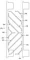
도 4는 도 3의 IV-IV'선에 대한 단면도이고,4 is a cross-sectional view taken along line IV-IV ′ of FIG. 3,
도 5는 본 발명의 다른 실시예에 따른 액정 표시 장치의 구조를 도시한 배치도이고,5 is a layout view illustrating a structure of a liquid crystal display according to another exemplary embodiment of the present invention.
도 6은 도 5의 액정 표시 장치를 VI-VI' 선을 따라 잘라 도시한 단면도이다.FIG. 6 is a cross-sectional view of the liquid crystal display of FIG. 5 taken along the line VI-VI '. FIG.
본 발명은 표시판 및 이를 포함하는 액정 표시 장치에 관한 것으로서, 특히 서로 마주하는 대향 전극과 화소 전극 중 화소 전극을 가지는 박막 트랜지스터 표 시판 및 이를 포함하는 액정 표시 장치에 관한 것이다.The present invention relates to a display panel and a liquid crystal display including the same, and more particularly, to a thin film transistor display panel having a pixel electrode among opposing electrodes and pixel electrodes facing each other, and a liquid crystal display including the same.
액정 표시 장치는 현재 가장 널리 사용되고 있는 평판 표시 장치 중 하나로서, 전계 생성 전극이 형성되어 있는 두 장의 표시판과 그 사이에 삽입되어 있는 액정층으로 이루어져, 전극에 전압을 인가하여 액정층의 액정 분자들을 재배열시킴으로써 액정층을 통과하는 빛의 투과율을 조절하는 표시 장치이다.The liquid crystal display is one of the most widely used flat panel display devices. The liquid crystal display includes two display panels on which a field generating electrode is formed and a liquid crystal layer interposed therebetween. It is a display device which controls the transmittance | permeability of the light which passes through a liquid crystal layer by rearranging.
액정 표시 장치 중에서도 현재 주로 사용되는 것은 전계 생성 전극이 두 표시판에 각각 구비되어 있는 것이다. 이중에서도 한 표시판에는 복수의 화소 전극이 행렬의 형태로 배열되어 있고 다른 표시판에는 하나의 공통 전극이 표시판 전면을 덮고 있는 구조의 액정 표시 장치가 주류이다. 이 액정 표시 장치에서의 화상의 표시는 각 화소 전극에 별도의 전압을 인가함으로써 이루어진다. 이를 위해서 화소 전극에 인가되는 전압을 스위칭하기 위한 삼단자 소자인 박막 트랜지스터를 각 화소 전극에 연결하고 이 박막 트랜지스터를 제어하기 위한 신호를 전달하는 게이트선과 화소 전극에 인가될 전압을 전달하는 데이터선을 표시판에 설치한다.Among the liquid crystal display devices, a field generating electrode is provided in each of two display panels. Among them, a liquid crystal display device having a structure in which a plurality of pixel electrodes are arranged in a matrix form on one display panel and one common electrode covering the entire display panel on the other display panel is mainstream. The display of an image in this liquid crystal display device is performed by applying a separate voltage to each pixel electrode. To this end, a thin film transistor, which is a three-terminal element for switching a voltage applied to a pixel electrode, is connected to each pixel electrode, and a gate line for transmitting a signal for controlling the thin film transistor and a data line for transmitting a voltage to be applied to the pixel electrode are provided. Install on the display panel.
그런데 액정 표시 장치는 시야각이 좁은 것이 중요한 단점이다. 이러한 단점을 극복하고자 시야각을 넓히기 위한 다양한 방안이 개발되고 있는데, 그 중에서도 액정 분자를 상하 기판에 대하여 수직으로 배향하고 화소 전극과 그 대향 전극인 공통 전극에 일정한 절개 패턴을 형성하거나 돌기를 형성하여 화소를 다중 도메인으로 분할하는 방법이 유력시되고 있다.However, it is an important disadvantage that the liquid crystal display device has a narrow viewing angle. In order to overcome these disadvantages, various methods for widening the viewing angle have been developed. Among them, the liquid crystal molecules are oriented vertically with respect to the upper and lower substrates, and the pixel is formed by forming a constant incision pattern or protrusion on the pixel electrode and the common electrode as the opposite electrode. The method of partitioning into multiple domains is gaining popularity.
그런데 이러한 액정 표시 장치는 시야각이 좁은 것이 중요한 단점이다. 이러한 단점을 극복하고자 시야각을 넓히기 위한 다양한 방안이 개발되고 있는데, 그 중에서도 액정 분자를 상하 표시판에 대하여 수직으로 배향하고 화소 전극과 그 대향 전극인 공통 전극에 일정한 절개 패턴을 형성하거나 돌기를 형성하는 방법이 유력시되고 있다.However, such a liquid crystal display device has a disadvantage that a narrow viewing angle is important. In order to overcome these disadvantages, various methods for widening the viewing angle have been developed. Among them, liquid crystal molecules are oriented vertically with respect to the upper and lower display panels, and a method of forming a constant incision pattern or forming protrusions on the pixel electrode and the common electrode that is opposite thereto. This is becoming potent.
절개 패턴을 형성하는 방법으로는 화소 전극과 공통 전극에 각각 절개 패턴을 형성하여 이들 절개 패턴으로 인하여 형성되는 프린지 필드(fringe field)를 이용하여 액정 분자들이 눕는 방향을 조절함으로써 시야각을 넓히는 방법이 있다.As a method of forming an incision pattern, an incision pattern is formed on each of the pixel electrode and the common electrode, and the viewing angle is widened by adjusting the direction in which the liquid crystal molecules lie down using a fringe field formed by the incision patterns. .
돌기를 형성하는 방법은 상하 표시판에 형성되어 있는 화소 전극과 공통 전극 위에 각각 돌기를 형성해 둠으로써 돌기에 의하여 왜곡되는 전기장을 이용하여 액정 분자의 눕는 방향을 조절하는 방식이다.The protrusions are formed by forming protrusions on the pixel electrode and the common electrode formed on the upper and lower display panels, respectively, to adjust the lying direction of the liquid crystal molecules using an electric field distorted by the protrusions.
또 다른 방법으로는, 하부 표시판 위에 형성되어 있는 화소 전극에는 절개 패턴을 형성하고 상부 표시판에 형성되어 있는 공통 전극 위에는 돌기를 형성하여 절개 패턴과 돌기에 의하여 형성되는 프린지 필드를 이용하여 액정의 눕는 방향을 조절함으로써 도메인을 형성하는 방식이 있다.In another method, an incision pattern is formed on the pixel electrode formed on the lower panel, and protrusions are formed on the common electrode formed on the upper panel, so that the liquid crystal lies down using a fringe field formed by the incision pattern and the protrusion. There is a way to form a domain by controlling.
이러한 액정 표시 장치에서 화소의 개구율을 확보하는 것이 중요한데, 이를 위하여 화소 전극과 데이터선의 서로 인접하게 또는 중첩하도록 배치하는데, 이로 인하여 화소 전압이 인가된 화소 전극과 연속적으로 변하는 데이터 전압이 전달되는 데이터선 사이에서 기생 용량이 형성되며, 이러한 기생 용량으로 인하여 여러 가지 불량이 발생한다. 하나의 예로, 액정 표시 장치의 제조 공정 중 사진 공정에서 기판의 액티브 영역보다 작은 노광 마스크를 이용하는 사진 식각 공정에서는 몇 개의 블록으로 나누어 노광 마스크를 이용한 노광 공정을 실시하게 되는데, 화소 전극과 데이터선사이의 거리가 블록마다 약간 달라질 수 있다. 이로 인하여 블록을 단위로 화소 전극과 데이터선 사이에서 발생하는 기생 용량의 차이가 발생하고 스티치 불량이 유발시킨다.In such a liquid crystal display, it is important to secure an aperture ratio of a pixel. For this purpose, the pixel electrode and the data line are arranged to be adjacent to or overlap with each other, whereby the data line to which the data voltage continuously changes with the pixel electrode to which the pixel voltage is applied is transferred. Parasitic capacitances are formed in between, and various defects occur due to such parasitic capacitances. For example, in a photolithography process using an exposure mask smaller than an active area of a substrate in a photolithography process of a liquid crystal display device, a photolithography process is performed by dividing into several blocks and performing an exposure process using an exposure mask. The distance can vary slightly from block to block. As a result, a difference in parasitic capacitance generated between the pixel electrode and the data line on a block basis causes a stitch defect.
또한, 이러한 액정 표시 장치에서는 데이터선과 화소 전극 또는 대향 전극 사이에 전계가 형성되는데, 이러한 전기장은 화소의 가장자리에 배치되어 있는 일부 액정 분자들의 배향을 왜곡시킨다. 이러한 배향 왜곡으로 인하여 화소의 둘레에서는 빛샘 현상이 나타나고, 이는 액정 표시 장치의 표시 특성을 저하시키는 원인으로 작용한다.In addition, in such a liquid crystal display, an electric field is formed between the data line and the pixel electrode or the counter electrode, and the electric field distorts the orientation of some liquid crystal molecules disposed at the edge of the pixel. Due to the alignment distortion, light leakage occurs around the pixel, which causes a decrease in display characteristics of the liquid crystal display.
또한, 이러한 액정 표시 장치는 화소가 항상 밝게 표시되거나 어둡게 표시되는 화소 불량이 발생하는데, 이를 최소화할 수 있는 화소 구조로 화소를 설계하는 것이 바람직하다.In addition, such a liquid crystal display may generate a pixel defect in which a pixel is always displayed brightly or darkly, and it is preferable to design the pixel to have a pixel structure that can minimize the pixel defect.
본 발명이 이루고자 하는 기술적 과제는 화소 전극과 데이터선 사이에서 발생하는 기생 용량의 변화 및 액정 분자의 배향 왜곡을 최소화할 수 있는 박막 트랜지스터 표시판 및 이를 포함하는 액정 표시 장치를 제공하는 것이다.SUMMARY OF THE INVENTION The present invention has been made in an effort to provide a thin film transistor array panel and a liquid crystal display including the same, which may minimize parasitic capacitance change and alignment distortion of liquid crystal molecules generated between a pixel electrode and a data line.
또한, 본 발명이 이루고자 하는 다른 기술적 과제는 화소 불량을 최소화할 수 있는 박막 트랜지스터 표시판 및 이를 포함하는 액정 표시 장치를 제공하는 것이다.Another object of the present invention is to provide a thin film transistor array panel capable of minimizing pixel defects and a liquid crystal display including the same.
이러한 과제를 해결하기 위하여 본 발명에서는 화소 전극과 동일한 층에 대 향 전극에 전달되는 공통 전압이 전달되는 보조 전극이 게이트선 및 데이터선의 상부에 배치되어 있다. 이때, 화소 전극과 보조 전극의 하부에 형성되어 있는 보호막은 일부 또는 전부가 제거되어 화소 전극과 보조 전극 사이에서 트랜치되어 있다.In order to solve this problem, in the present invention, an auxiliary electrode to which the common voltage transferred to the counter electrode is transferred to the same layer as the pixel electrode is disposed on the gate line and the data line. In this case, some or all of the passivation layer formed under the pixel electrode and the auxiliary electrode is removed to be trenched between the pixel electrode and the auxiliary electrode.
더욱 상세하게, 본 발명의 실시예에 따른 박막 트랜지스터 표시판에는 절연 기판 상부에 주사 신호를 전달하는 게이트선이 형성되어 있고, 게이트선과 교차하며 영상 신호를 전달하는 데이터선이 형성되어 있다. 게이트선과 데이터선이 정의하는 화소에는 화소 전극과 게이트선에 연결되어 있는 게이트 전극, 데이터선의 일부로 연결된 소스 전극 및 화소 전극에 연결되어 있는 드레인 전극을 포함하는 박막 트랜지스터가 형성되어 있으며, 게이트선, 데이터선 및 박막 트랜지스터를 덮는 보호막의 상부에는 박막 트랜지스터와 전기적으로 연결되어 있는 화소 전극과 게이트선 및 데이터선을 중첩하는 있는 보조 전극이 형성되어 있다. 이때, 화소 전극과 보조 전극 사이의 보호막은 일부 또는 전부가 제거되어 트랜치되어 있다.More specifically, in the thin film transistor array panel according to the exemplary embodiment of the present invention, a gate line for transmitting a scan signal is formed on an insulating substrate, and a data line for intersecting the gate line and transmitting an image signal is formed. In the pixel defined by the gate line and the data line, a thin film transistor including a pixel electrode and a gate electrode connected to the gate line, a source electrode connected as part of the data line, and a drain electrode connected to the pixel electrode is formed. A pixel electrode electrically connected to the thin film transistor and an auxiliary electrode overlapping the gate line and the data line are formed on the passivation layer covering the line and the thin film transistor. In this case, a part or all of the passivation layer between the pixel electrode and the auxiliary electrode is removed and trenched.
이때, 화소 전극의 모서리는 모따기 구조로 이루어진 것이 바람직하다.In this case, the edge of the pixel electrode preferably has a chamfer structure.
절연막은 유기 절연 물질로 이루어진 것이 바람직하며, 유기 절연 물질은 색 필터를 포함할 수 있다.Preferably, the insulating film is made of an organic insulating material, and the organic insulating material may include a color filter.
화소 전극과 중첩하여 유지 용량을 형성하는 유지 전극을 더 포함할 수 있으며, 보조 전극과 유지 전극은 서로 전기적으로 연결되어 있는 것이 바람직하다.The storage electrode may further include a storage electrode overlapping the pixel electrode to form the storage capacitor, and the auxiliary electrode and the storage electrode may be electrically connected to each other.
데이터선과 중첩하는 보조 전극의 경계는 데이터선을 완전히 덮는 것이 바람직하며, 게이트선과 중첩하는 보조 전극의 경계는 게이트선 안쪽에 배치되어 있는 것이 바람직하다.It is preferable that the boundary of the auxiliary electrode overlapping the data line completely covers the data line, and the boundary of the auxiliary electrode overlapping the gate line is preferably disposed inside the gate line.
화소 전극은 게이트선에 대하여 실질적으로 ±45도를 이루는 도메인 규제 수단을 가지는 것이 바람직하다.It is preferable that the pixel electrode has domain regulating means substantially at +/- 45 degrees with respect to the gate line.
본 발명의 실시예에 따른 액정 표시 장치는 앞에서 설명한 박막 트랜지스터 표시판과 이와 마주하며 화소 전극과 마주하는 공통 전극을 가지는 대향 표시판과 박막 트랜지스터 표시판과 공통 전극 표시판 사이에 형성되어 있는 액정층을 포함한다.The liquid crystal display according to the exemplary embodiment of the present invention includes a liquid crystal layer formed between the thin film transistor array panel and the opposite display panel having the common electrode facing the pixel electrode, and the thin film transistor array panel and the common electrode display panel.
공통 전극과 상기 보조 전극은 동일한 신호가 전달되는 것이 바람직하며, 액정층에 포함되어 있는 액정은 음의 유전율 이방성을 가지며 액정의 그 장축이 두 표시판에 대하여 수직으로 배향되어 있는 것이 바람직하다.It is preferable that the common electrode and the auxiliary electrode transmit the same signal, and the liquid crystal included in the liquid crystal layer has negative dielectric anisotropy, and its long axis is preferably perpendicular to the two display panels.
공통 전극과 화소 전극은 액정층의 액정 분자를 분할 배향하여 화소를 다수의 도메인으로 분할하는 도메인 규제 수단을 가지는 것이 바람직하며, 도메인 규제 수단은 절개부일 수 있다.The common electrode and the pixel electrode preferably have domain regulating means for dividing and aligning the liquid crystal molecules of the liquid crystal layer into a plurality of domains. The domain regulating means may be a cutout.
박막 트랜지스터 표시판은 게이트 전극과 소스 및 드레인 전극 사이에 형성되어 있는 반도체를 더 포함하는데, 반도체는 데이터선의 하부까지 연장될 수 있으며, 소스 전극과 드레인 전극 사이의 채널부를 제외한 반도체는 데이터선과 드레인 전극과 동일한 패턴을 가질 수 있다.The thin film transistor array panel further includes a semiconductor formed between the gate electrode and the source and drain electrodes. The semiconductor may extend to the lower portion of the data line, and the semiconductor except for the channel portion between the source electrode and the drain electrode may include the data line and the drain electrode. It can have the same pattern.
첨부한 도면을 참고로 하여 본 발명의 실시예에 대하여 본 발명이 속하는 기술 분야에서 통상의 지식을 가진 자가 용이하게 실시할 수 있도록 상세히 설명한다. 그러나 본 발명은 여러 가지 상이한 형태로 구현될 수 있으며 여기에서 설명 하는 실시예에 한정되지 않는다.DETAILED DESCRIPTION Embodiments of the present invention will be described in detail with reference to the accompanying drawings so that those skilled in the art may easily implement the present invention. As those skilled in the art would realize, the described embodiments may be modified in various different ways, all without departing from the spirit or scope of the present invention.
도면에서 여러 층 및 영역을 명확하게 표현하기 위하여 두께를 확대하여 나타내었다. 명세서 전체를 통하여 유사한 부분에 대해서는 동일한 도면 부호를 붙였다. 층, 막, 영역, 판 등의 부분이 다른 부분 "위에" 있다고 할 때, 이는 다른 부분 "바로 위에" 있는 경우뿐 아니라 그 중간에 또 다른 부분이 있는 경우도 포함한다. 반대로 어떤 부분이 다른 부분 "바로 위에" 있다고 할 때에는 중간에 다른 부분이 없는 것을 뜻한다.In the drawings, the thickness of layers, films, panels, regions, etc., are exaggerated for clarity. Like parts are designated by like reference numerals throughout the specification. When a part of a layer, film, region, plate, etc. is said to be "on" another part, this includes not only the other part being "right over" but also another part in the middle. On the contrary, when a part is "just above" another part, there is no other part in the middle.
그러면 도면을 참고로 하여 본 발명의 실시예에 따른 다중 도메인 액정 표시 장치에 대하여 설명한다.Next, a multi-domain liquid crystal display according to an exemplary embodiment of the present invention will be described with reference to the drawings.
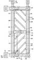
도 1은 본 발명의 한 실시예에 따른 액정 표시 장치용 박막 트랜지스터 표시판의 구조를 도시한 배치도이고, 도 2는 본 발명의 한 실시예에 따른 액정 표시 장치용 대향 표시판의 구조를 도시한 배치도이고, 도 3은 본 발명의 도 1 및 도 2의 표시판을 정렬하여 완성한 한 실시예에 따른 액정 표시 장치의 구조를 도시한 배치도이고, 도 4는 도 3의 액정 표시 장치를 IV-IV'선을 따라 잘라 도시한 단면도이다.1 is a layout view showing a structure of a thin film transistor array panel for a liquid crystal display according to an exemplary embodiment of the present invention, and FIG. 2 is a layout view showing a structure of an opposing display panel for a liquid crystal display according to an exemplary embodiment of the present invention. 3 is a layout view illustrating a structure of a liquid crystal display according to an exemplary embodiment in which the display panels of FIGS. 1 and 2 are aligned, and FIG. 4 is a line IV-IV 'of the liquid crystal display of FIG. It is a cross-sectional view cut along.
액정 표시 장치는 하측의 박막 트랜지스터 표시판(100)과 이와 마주보고 있는 상측의 대향 표시판(200) 및 이들 사이에 형성되어 있으며, 두 표시판(100, 200)에 대하여 거의 수직으로 배향되어 있는 액정 분자(310)를 포함하는 액정층(3)으로 이루어진다. 이때, 각각의 표시판(100, 200)에는 배향막(11, 21)이 형성되어 있으며, 배향막(11, 21)은 액정층(3)의 액정 분자(310)를 표시판(100, 200)에 대하 여 수직으로 배향되도록 하는 수직 배향 모드인 것이 바람직하나, 그렇지 않을 수도 있다. 또한, 상부 표시판(200)과 하부 표시판(100)의 바깥 면에는 각각 상부 및 하부 편광판(12. 22)이 부착되어 있다.The liquid crystal display device is formed of a liquid crystal molecule that is formed between the thin film
박막 트랜지스터 표시판(100)에는 ITO(indium tin oxide)나 IZO(indium zinc oxide) 등의 투명한 도전 물질로 이루어져 있으며 절개부(191, 192, 193, 194, 195, 196, 197, 198))를 가지고 있는 화소 전극(190)이 형성되어 있고, 각 화소 전극(190)은 박막 트랜지스터에 연결되어 화상 신호 전압을 인가 받는다. 이 때, 박막 트랜지스터는 주사 신호를 전달하는 게이트선(121)과 화상 신호를 전달하는 데이터선(171)에 각각 연결되어 주사 신호에 따라 화소 전극(190)을 온(on)오프(off)한다. 여기서, 화소 전극(190)은 반사형 액정 표시 장치인 경우 투명한 물질로 이루어지지 않을 수도 있고, 이 경우에는 하부 편광판(12)도 불필요하게 된다.The thin film
역시, 박막 트랜지스터 표시판(100)과 마주하는 대향 표시판(200)에는 화소의 가장자리에서 발생하는 빛샘을 방지하기 위한 블랙 매트릭스(220)와 적, 녹, 청의 색 필터(230) 및 ITO 또는 IZO 등의 투명한 도전 물질로 이루어져 있는 대향 전극(270)이 형성되어 있다. 블랙 매트릭스(220)는 화소 영역의 둘레 부분뿐만 아니라 대향 전극(270)의 절개부(271, 272, 273, 274, 275, 276, 277, 278)와 중첩하는 부분에도 형성할 수 있다. 이는 절개부(271, 272, 273, 274, 275, 276, 277, 278)로 인해 발생하는 빛샘을 방지하기 위함이다.Also, the opposing
다음은 도 1, 도 3 및 도 4를 참조하여 박막 트랜지스터 표시판(100)에 대하여 좀 더 상세히 한다.Next, the thin film
박막 트랜지스터 표시판(100)에는 하부 절연 기판(110) 위에 게이트 신호를 전달하는 복수의 게이트선(gate line)(121)이 형성되어 있다. 게이트선(121)은 주로 가로 방향으로 뻗어 있으며, 각 게이트선(121)의 일부는 복수의 게이트 전극(gate electrode)(124)을 이룬다. 게이트선(121)에는 게이트 전극(124)은 돌기의 형태로 형성되어 있고, 본 실시예와 같이 게이트선(121)은 외부로부터의 게이트 신호를 게이트선(121)으로 전달하기 위한 접촉부를 가질 수 있으며, 이때 게이트선(121)의 끝 부분(129)은 다른 부분보다 넓은 폭은 가지는 것이 바람직하며, 기판(110) 상부에 게이트 구동 회로가 형성되어 있는 실시예에서 게이트선(121)은 게이트 구동 회로의 출력단에 전기적으로 연결된다.In the thin film
절연 기판(110) 위에는 게이트선(121)과 동일한 층으로 게이트선(121)과 전기적으로 분리된 복수의 유지 전극선(131)이 형성되어 있으며, 이러한 유지 전극선(131)은 드레인 전극(175)과 중첩시켜 유지 축전기를 만드는 유지 전극(133)을 포함한다. 유지 전극선(131)은 공통 전압 따위의 미리 정해진 전압을 외부로부터 인가 받으며, 화소 전극(190)과 게이트선(121)의 중첩으로 발생하는 유지 용량이 충분할 경우 유지 전극선(131)은 생략할 수도 있으며, 화소의 개구율을 극대화하기 위해 화소 영역의 가장자리에 배치할 수도 있다.On the insulating
각 유지 전극선(131)은 이후에 형성되는 화소 전극(190)의 절개부(191, 192, 193, 194, 195, 196, 197, 198)와 중첩하며 화소에서 누설되는 빛을 차단하는 유지 전극을 포함할 수 있다.Each
게이트선(121) 및 유지 전극선(131)은 Al, Al 합금, Ag, Ag 합금, Cr, Ti, Ta, Mo 등의 금속 따위로 만들어진다. 도 4에 나타난 바와 같이, 본 실시예의 게이트선(121) 및 유지 전극 배선(131, 133a, 133b, 133c, 133d)은 단일층으로 이루어지지만, 물리 화학적 특성이 우수한 Cr, Mo, Ti, Ta 등의 금속층과 비저항이 작은 Al 계열 또는 Ag 계열의 금속층을 포함하는 이중층으로 이루어질 수도 있다. 이외에도 여러 다양한 금속 또는 도전체로 게이트선(121)과 유지 전극선(131)을 만들 수 있다.The
게이트선(121)과 유지 전극선(131)이 측면은 경사져 있으며 수평면에 대한 경사각은 30-80°인 것이 바람직하다.The sidewalls of the
게이트선(121)과 유지 전극 배선(131)의 위에는 질화규소(SiNx) 등으로 이루어진 게이트 절연막(140)이 형성되어 있다.A
게이트 절연막(140) 위에는 복수의 데이터선(171)을 비롯하여 복수의 드레인 전극(drain electrode, 175)이 형성되어 있다. 각 데이터선(171)은 주로 세로 방향으로 뻗어 있으며, 각 드레인 전극(175)을 향하여 복수의 분지를 내어 데이터선(171)으로부터 확장된 소스 전극(source electrode)(173)을 가진다. 데이터선(171)의 한쪽 끝 부분에 위치한 접촉부(179)는 외부로부터의 화상 신호를 데이터선(171)에 전달한다.A plurality of
데이터선(171), 드레인 전극(175)도 게이트선(121)과 마찬가지로 크롬과 알루미늄 등의 도전 물질을 포함하는 금속으로 만들어지며, 단일층 또는 다중층으로 이루어질 수 있다.Like the
데이터선(171), 드레인 전극(175)의 아래에는 데이터선(171)을 따라 주로 세 로로 길게 뻗은 복수의 섬형 반도체(155)가 형성되어 있다. 비정질 규소 따위로 이루어진 각 섬형 반도체(154)는 각 게이트 전극(124), 소스 전극(173) 및 드레인 전극(175)을 향하여 확장되어 있으며, 박막 트랜지스터의 채널이 형성되는 채널부를 가진다. 이때, 섬형 반도체(154)는 데이터선(171)과 교차하는 데이터선(171)을 덮고 있으며, 데이터선(171)의 모양을 따라 선형으로 형성될 수 있다. 또한, 섬형 반도체(154)의 대부분은 게이트 전극(124)의 경계선 안쪽에 위치하는 것이 바람직하다.Below the
반도체(151)와 데이터선(171) 및 드레인 전극(175) 사이에는 둘 사이의 접촉 저항을 각각 감소시키기 위한 복수의 섬형 저항성 접촉 부재(ohmic contact)(163, 165)가 형성되어 있다. 저항성 접촉 부재(161)는 실리사이드나 n형 불순물이 고농도로 도핑된 비정질 규소 따위로 만들어지며, 섬형의 저항성 접촉 부재(163, 165)는 게이트 전극(124)을 중심으로 서로 마주한다.A plurality of island-like
데이터선(171) 및 드레인 전극(175) 위에는 평탄화 특성이 우수하며 감광성을 가지는 유기 물질, 플라스마 화학 기상 증착(plasma enhanced chemical vapor deposition, PECVD)으로 형성되는 a-Si:C:O, a-Si:O:F 등의 저유전율 절연 물질로 이루어진 보호막(180)이 형성되어 있다. 이때, 보호막(180)은 게이트선(121) 및 데이터선(171)의 둘레에 트랜치(188)를 가지며, 이러한 트랜치(188)는 이후에 형성되는 화소 전극(190)과 보조 전극(199) 사이에 위치하며, 제조 공정시 화소 전극(190)과 보조 전극(199)의 단락을 방지하여 화소 불량을 최소화하기 위함이며, 이후의 제조 공정을 통하여 구체적으로 설명하기로 한다.On the
보호막(180)은 소스 전극(173)과 드레인 전극(175) 사이로 드러난 반도체(154)를 덮는 절연막을 포함하는 것이 바람직하며, 이러한 절연막을 박막 트랜지스터의 특성을 안정적으로 확보하기 위함이며, 질화 규소로 이루어진 것이 바람직하며, 이후의 실시예를 통하여 구체적으로 설명하기로 한다.The
또한, 보호막(180)은 아크릴계의 유기 절연 물질로 이루어질 수 있으며, 적색, 녹색, 청색의 안료를 포함하여 이루어진 색필터를 포함할 수 있다.In addition, the
보호막(180)에는 드레인 전극(175)의 적어도 일부와 데이터선(171)의 끝 부분(179)을 각각 노출시키는 복수의 접촉 구멍(185, 182)이 구비되어 있다. 한편, 게이트선(121)의 끝 부분(129)도 외부의 구동 회로와 연결되기 위한 접촉부를 가지데, 복수의 접촉 구멍(181)이 게이트 절연막(140)과 보호막(180)을 관통하여 게이트선(121)의 끝 부분을 드러낸다.The
보호막(180) 위에는 절개부(191, 192, 193, 194, 195, 196, 197, 198)를 가지는 복수의 화소 전극(190)을 비롯하여 복수의 데이터 접촉 보조 부재(82, 81)가 형성되어 있다. 화소 전극(190)과 데이터 접촉 보조 부재(81, 82)는 ITO(indium tin oxide)나 IZO(indium zinc oxide) 등과 같은 투명 도전체나 알루미늄(Al)과 같은 광 반사 특성이 우수한 불투명 도전체를 사용하여 형성한다.A plurality of
화소 전극(190)에 형성되어 있는 절개부(191, 192, 193, 194, 195, 196, 197, 198)는 화소 전극(190)을 상하로 반분하는 가로 선에 대하여 대칭을 이루며, 각각 사선 방향으로 형성되어 있다. 절개부(194, 195)는 화소 전극(190)의 왼쪽 변에서 오른쪽 변을 향하여 파고 들어간 단부를 포함한다. 따라서, 화소 전극 (190)은 각각 게이트선(121)과 데이터선(171)이 교차하여 정의하는 화소 영역을 상하로 이등분하는 선(게이트선과 나란한 선)에 대하여 실질적으로 거울상 대칭을 이루고 있다.The
이 때, 화소 영역에서 상하의 절개부(191, 192, 193, 194, 195, 196, 197, 198)는 서로 수직을 이루고 있는데, 이는 프린지 필드의 방향을 4 방향으로 고르게 분산시키기 위함이다.In this case, the upper and
또, 화소 전극(190)과 동일한 층에는 상부 표시판(200)의 대향 전극(270)에 전달되는 공통 전압이 전달되는 보조 전극(199)이 형성되어 있다. 보조 전극(199)가로 방향의 게이트선(121)과 세로 방향의 데이터선(191)과 중첩하여 그물 모양을 가지고 있는데, 게이트선(121)과 중첩하는 부분은 게이트선(121)의 경계선 안에 위치하며, 데이터선(171)과 중첩하는 부분은 데이터선(171)을 완전히 덮어 경계선이 데이터선(171)의 경계선 밖에 위치한다.In addition, an
이러한 본 발명의 실시예에 따른 박막 트랜지스터 표시판에서는, 데이터선(171)보다 보조 전극(199)이 화소 전극(190)의 경계에 더욱 인접하게 배치되어 있어, 데이터선(171)과 화소 전극(190) 사이에 위치하는 액정 분자들은 보조 전극(199)과 화소 전극(190) 사이에 형성되는 전기장에 의해 구동되며, 이러한 전기장은 기판(110) 면에 대하여 거의 평행하게 형성된다. 따라서, 데이터선(171)과 화소 전극(190) 사이에 위치하는 액정 분자들은 두 표시판(100, 200)에 대하여 수직하게 배열된 상태를 유지하며, 이로 인하여 보조 전극(199)과 화소 전극(190) 사이는 어둡게 표시되며, 누설되는 빛이 발생하지 않아 액정 표시 장치의 표시 특성을 향상시킬 수 있다. 또한, 이를 통하여 대향 표시판(200)에 형성되어 있는 블랙 매트릭스(220)의 폭을 최소의 폭으로 설계할 수 있어, 화소의 개구율을 극대화할 수 있다.In the thin film transistor array panel according to the exemplary embodiment of the present invention, the
또한, 데이터선(171)보다 보조 전극(199)이 화소 전극(190)의 경계에 더욱 인접하게 배치되어 있어 데이터선(171)과 화소 전극(190) 사이에 형성되는 전기장은 차단되어, 데이터선(171)과 화소 전극(190) 사이에서 형성되는 커플링 용량을 발생하지 않으며, 이를 통하여 스티치 불량을 방지할 수 있다.In addition, since the
또한, 화소 전극(190)의 모서리(A)는 모따기 구조를 취하고 있어, 제조 공정시 제조 공정시 패턴의 해상도를 극대화할 수 있으며, 보조 전극(199)과 화소 전극(190)의 단락 확률을 최소화할 수 있으며, 단락(short)이 발생하더라도 단락을 검출하기가 용이함과 동시에 단락을 수리하기도 용이하며, 이에 대해서는 제조 공정을 설명할 때 보다 구체적으로 설명하기로 한다.In addition, the corner A of the
한편, 박막 트랜지스터 표시판(100)과 마주하는 대향 표시판(200)에는 상부의 절연 기판(210)에 화소 가장자리에서 빛이 새는 것을 방지하기 위한 블랙 매트릭스(220)가 형성되어 있다. 블랙 매트릭스(220)의 위에는 적, 녹, 청색의 색 필터(230)가 형성되어 있다. 색 필터(230)의 위에는 전면적으로 평탄화막(250)이 형성되어 있고, 그 상부에는 절개부(271, 272, 273)를 가지는 기준 전극(270)이 형성되어 있다. 기준 전극(270)은 ITO 또는 IZO(indium zinc oxide) 등의 투명한 도전체로 형성한다.In the
공통 전극(270)의 한 벌의 절개부(271, 272, 273, 274, 275, 276, 277, 278) 는 화소 전극(190)의 절개부(191, 192, 193, 194, 195, 196, 197, 198) 중 게이트선(121)에 대하여 45°를 이루는 부분과 교대로 배치되어 이와 나란한 사선부와 화소 전극(190)의 변과 중첩되어 있는 단부를 포함하고 있다. 이 때, 단부는 세로 방향 단부와 가로 방향 단부로 분류된다.The
이상과 같은 구조의 박막 트랜지스터 기판과 대향 표시판을 정렬하여 결합하고 그 사이에 액정 물질을 주입하여 수직 배향하면 본 발명에 따른 액정 표시 장치의 기본 구조가 마련된다.When the thin film transistor substrate and the opposing display panel having the above structure are aligned and combined, and a liquid crystal material is injected and vertically aligned therebetween, a basic structure of the liquid crystal display according to the present invention is provided.
박막 트랜지스터 표시판(100)과 대향 표시판(200)을 정렬했을 때 화소 전극(190)의 절개부(191, 192, 193, 194, 195, 196, 197, 198)와 대향 전극(270)의 절개부(271, 272, 273, 274, 275, 276, 277, 278)는 화소 영역을 다수의 도메인으로 분할한다. 이들 도메인은 그 내부에 위치하는 액정 분자의 평균 장축 방향에 따라 4개의 종류로 분류되며, 각각의 도메인은 길쭉하게 형성되어 폭과 길이를 가진다.When the thin film
이 때, 화소 전극(190)의 절개부(191, 192, 193, 194, 195, 186, 197, 198)와 공통 전극(270)의 절개부(271, 272, 273, 274, 275, 276, 277, 278)는 액정 분자를 분할 배향하는 도메인 규제 수단으로서 작용하며, 도메인 규제 수단으로는 절개부 대신 화소 전극(190) 및 공통 전극(270)의 상부 또는 하부에 무기 물질 또는 유기 물질로 돌기를 형성하는 경우에는 폭을 5㎛에서 10㎛ 사이로 하는 것이 바람직하다.In this case, the
이러한 본 발명의 실시예에 따른 액정 표시 장치에서, 보조 전극(199)과 공통 전극(270)에는 서로 동일한 전압이 인가되어, 액정 표시 장치의 구동시 화소 전 극(190)에 구동 전압이 인가되더라도 보조 전극(199)과 공통 전극(270) 사이의 액정 분자들은 움직이지 않고 표시판(100, 200)에 수직하게 배열되어 있는 수직 배향 모드를 유지한다. 따라서, 보조 전극(199)에 대응하는 부분은 어둡게 표시되어, 서로 이웃하는 화소 영역 사이에서는 빛샘이 발생하지 않으며, 이를 통하여 액정 표시 장치의 표시 특정을 향상시킬 수 있다.In the liquid crystal display according to the exemplary embodiment of the present invention, the same voltage is applied to the
이러한 구조의 본 실시예에 따른 액정 표시 장치에 있어서 박막 트랜지스터 표시판을 제조하는 방법에 대하여 개략적으로 설명하면 다음과 같다.A method of manufacturing a thin film transistor array panel in the liquid crystal display according to the exemplary embodiment of such a structure will be described as follows.
먼저, 하부 절연 기판(110) 상부에 Cr 또는 Mo 합금 등으로 이루어지는 도전막과 저항이 작은 Al 또는 Ag 또는 이들을 포함하는 합금 등으로 이루어지는 도전막을 스퍼터링 따위의 방법으로 단일막 또는 다층막으로 적층하고 마스크를 이용한 사진 식각 공정으로 건식 또는 습식 식각을 이용하여 게이트선(121)과 유지 전극선(131)을 형성한다.First, a conductive film made of Cr or Mo alloy or the like and a conductive film made of Al or Ag having a low resistance or an alloy containing them are laminated on the lower insulating
다음, 게이트 절연막(140), 수소화 비정질 규소층 및 인(P) 따위의 n형 불순물이 고농도로 도핑되어 있는 비정질 규소층을 화학 기상 증착법을 이용하여 각각 1,500 Å 내지 5,000 Å, 500 Å 내지 2,000 Å, 300 Å 내지 600 Å의 두께로 연속 증착하고, 마스크를 이용한 사진 식각 공정으로 도핑된 비정질 규소층과 비정질 규소층을 차례로 패터닝하여 채널부가 연결되어 있는 저항성 접촉층과 비정질 규소의 섬형 반도체(154)를 형성한다.Next, the
이어, Cr 또는 Mo 합금 등으로 이루어지는 도전막 또는 저항이 작은 Al 또는 Ag 또는 이들을 포함하는 합금 등으로 이루어지는 도전막 따위를 스퍼터링 등의 방 법으로 단층 또는 다층으로 1,500 Å 내지 3,000 Å의 두께로 증착한 다음 마스크를 이용한 사진 식각 공정으로 패터닝하여 데이터선(171) 및 드레인 전극(175)을 형성한다.Subsequently, a conductive film made of Cr or Mo alloy or the like or a conductive film made of Al or Ag having low resistance or an alloy containing them is deposited to a thickness of 1,500 kPa to 3,000 kPa in a single layer or multiple layers by sputtering or the like. Next, the
이어, 소스 전극(173)과 드레인 전극(175)으로 가려지지 않은 저항성 접촉층을 식각하여 소스 전극(173)과 드레인 전극(175) 사이의 반도체(154)를 드러내고 양쪽으로 분리된 저항성 접촉층(163, 165)을 형성한다.Subsequently, the ohmic contact layer that is not covered by the
이어, 평탄화 특성이 우수하고 감광성을 가지는 유기 절연 물질을 도포하여 보호막(180)을 형성하고, 광마스크를 이용한 사진 공정으로 보호막(180)을 노광하고 현상하여 접촉구(181, 182, 185)를 형성한다. 이때, 접촉구(181, 182, 185)를 형성할 때, 화소의 가장자리 중 게이트선(121) 및 데이터선(171)의 모양을 따라 게이트선(121) 및 데이터선(171)의 양쪽에 트랜치(188)를 형성한다. 여기서, 유기 절연 물질을 도포하기 전에 질화 규소 또는 산화 규소를 화학 기상 증착 등의 방법으로 적층하여 소스 전극(173)과 드레인 전극(175) 사이로 노출되는 반도체(154)를 덮는 절연막을 추가로 형성하는 것이 바람직하다.Subsequently, a
다음, 도 1, 도 3 및 도 4에서 보는 바와 같이, ITO 또는 IZO를 400 Å 내지 500 Å 두께로 증착하고 마스크를 이용한 사진 식각하여 모서리(A)에 모따기 구조를 가지는 화소 전극(190), 보조 전극(199)과 접촉 보조 부재(81, 82)를 형성한다. 이때, 화소 전극(190)과 보조 전극(199) 사이의 보호막(180)에는 트랜치(188)가 화소 전극(190)과 보조 전극(199) 사이에 도전성 입자가 잔류하더라도 도전성 입자는 트랜치(188) 내에 형성되어, 화소 전극(190)과 보조 전극(199)은 서로 단락되지 않 아, 단락으로 인한 화소 불량을 최소화할 수 있다.Next, as shown in FIGS. 1, 3, and 4, the ITO or IZO is deposited to a thickness of 400 to 500 하고 and photo-etched using a mask to etch the
이때, 모따기의 크기는 40-10㎛ 범위인 것이 바람직하며, 화소 전극(190)의 모서리에서 화소 전극(190)과 보조 전극(199)이 단락되는 것을 방지하기 위해 사진 식각 공정에서 감광막을 노광하기 위해 사용하는 노광기의 분해능보다 2배 이상의 크기로 모따기를 형성하는 것이 바람직하다.At this time, the size of the chamfer is preferably in the range of 40-10 μm, and in order to prevent the
이러한 본 발명의 실시예에 따른 박막 트랜지스터 표시판의 제조 방법에서는 화소 전극(190)의 모서리를 노광기의 분해능보다 2배 이상의 크기를 가지는 모따기 구조로 형성함으로써 화소 전극(190)의 모서리에서 도전성 패턴이 잔류할 확률을 최소화할 수 있으며, 이를 화소 전극(190)과 보조 전극(199)이 서로 단락되는 것을 방지할 수 있으며, 화소 전극(190)과 보조 전극(199)의 해상도를 극대화할 수 있다.In the method of manufacturing the thin film transistor array panel according to the exemplary embodiment of the present invention, the edge of the
또한, 화소 전극(190)과 보조 전극(199)이 서로 단락되더라도 화소 전극(190)의 모서리에서 보조 전극(199)과 화소 전극(190)의 간격을 넓게 확보하여, 화소 전극(190)의 모서리에서 단락이 발생하더라도 저배율을 광학기를 이용하여 용이하게 단락 위치를 검출하여 광학기의 검출력을 향상시킬 수 있다. 또한, 단락을 수리하기 위해 레이저(Laser)를 이용하여 화소 전극(190)과 보조 전극(190)을 용이하게 단선시킬 수 있다.In addition, even when the
한편, 본 발명의 실시예에서 박막 트랜지스터 표시판은 다른 모양을 가질 수 있으며, 하나의 실시예를 도면을 참조하여 구체적으로 설명하기로 한다.Meanwhile, in the exemplary embodiment of the present invention, the TFT panel may have a different shape, and one embodiment will be described in detail with reference to the accompanying drawings.
도 5는 본 발명의 다른 실시예에 따른 액정 표시 장치의 배치도이고, 도 6은 도 5의 액정 표시 장치를 VI-VI' 선을 따라 잘라 도시한 단면도이다.5 is a layout view of a liquid crystal display according to another exemplary embodiment. FIG. 6 is a cross-sectional view of the liquid crystal display of FIG. 5 taken along the line VI-VI ′.
도 5 내지 도 6에서 보는 바와 같이, 본 실시예에 따른 액정 표시 장치의 박막 트랜지스터 표시판의 층상 구조는 대개 도 1 내지 도 4에 도시한 액정 표시 장치의 박막 트랜지스터 표시판의 층상 구조와 동일하다. 즉, 기판(110) 위에 복수의 게이트 전극(124)을 포함하는 복수의 게이트선(121)이 형성되어 있고, 게이트 절연막, 반도체(154) 및 저항성 접촉 부재(163, 165)가 형성되어 있다. 저항성 접촉 부재(163, 165) 및 게이트 절연막(140) 위에는 복수의 소스 전극(173)을 포함하는 복수의 데이터선(171) 및 복수의 드레인 전극(175)이 형성되어 있고 그 위에 보호막(180)이 형성되어 있다. 보호막(180)에는 화소 전극(190)과 보조 전극(199) 사이에 트랜치(188)가 형성되어 있으며, 보호막(180) 및/또는 게이트 절연막(140)에는 복수의 접촉 구멍(182, 181, 185)이 형성되어 있으며, 그 상부에는 화소 전극(190)과 보조 전극(199)과 접촉 보조 부재(81, 82)가 형성되어 있다.5 to 6, the layer structure of the thin film transistor array panel of the liquid crystal display according to the present exemplary embodiment is generally the same as the layer structure of the thin film transistor array panel of the liquid crystal display shown in FIGS. 1 to 4. That is, the plurality of
그러나, 보호막(180)은 질화 규소 또는 산화 규소로 이루어진 제1 절연막(801)과 유기 절연 물질로 이루어진 제2 절연막(802)으로 이루어져 있는데, 트랜치(188)는 제2 절연막(802)에만 형성되어 있으며, 제1 절연막(801)에는 형성되어 있지 않다. 따라서, 본 실시예에서는 보호막(180)의 일부에만 트랜치(188)가 형성되어 있는 구조이다.However, the
또한, 게이트 절연막(140) 위에는 복수의 섬형 반도체(154)는 복수의 선형 반도체(151)와 연결되어 있고, 복수의 섬형 접촉 부재(163) 또한 복수의 선형 저항성 접촉 부재(161)와 연결되어 있다. 이때, 반도체(151)는 박막 트랜지스터가 위 치하는 채널부(154)를 제외하면 데이터선(171), 드레인 전극(175) 및 그 하부의 저항성 접촉 부재(161, 165,)와 실질적으로 동일한 평면 형태를 가지고 있다. 구체적으로는, 선형 반도체(151)는 데이터선(171) 및 드레인 전극(175)과 그 하부의 저항성 접촉 부재(161, 165)의 아래에 존재하는 부분 외에도 소스 전극(173)과 드레인 전극(175) 사이에 이들에 가리지 않고 노출된 부분을 가지고 있다.In addition, the plurality of island-
이러한 본 발명의 다른 실시예에 따른 액정 표시 장치의 박막 트랜지스터 표시판은 제조 공정에서 데이터선(171)과 반도체(151)를 부분적으로 위치에 따라 다른 두께를 가지는 감광막 패턴을 이용한 사진 식각 공정으로 함께 패터닝하여 형성한 것이다.The thin film transistor array panel of the liquid crystal display according to another exemplary embodiment of the present invention is patterned together in a photolithography process using a photoresist pattern having a different thickness depending on the position of the
한편, 본 발명의 실시예에서는 액정 분자가 두 표시판(100, 200)에 대하여 수직하게 배열되어 있는 수직 배향 모드의 액정 표시 장치에 대해서만 설명하였지만, 데이터선(171)을 완전히 덮으며, 공통 전압이 전달되는 보조 전극을 형성하거나, 화소 전극의 모서리를 모따기 구조로 형성하는 본원의 구성은 두 표시판에 대하여 액정 분자를 평행하면서 나선형으로 비틀려 배열하는 비틀린 네마틱 방식(twisted nematic mode), 공통 전극과 화소 전극을 동일한 표시판에 배치하여 표시판에 평행하게 배열되어 있는 액정 분자를 구동하는 평면 구동 방식(in-plane switching mode) 등의 다양한 방식의 액정 표시 장치에 적용할 수 있다.Meanwhile, in the exemplary embodiment of the present invention, only the liquid crystal display device in the vertical alignment mode in which the liquid crystal molecules are vertically arranged with respect to the two
이상과 같이, 본 발명의 실시예에서는 화소 전극과 보조 전극 사이의 보호막에 트랜치를 형성함으로써 화소 전극과 보조 전극이 단락되는 것을 방지하여 화소 불량을 최소화할 수 있다.As described above, in the exemplary embodiment of the present invention, a trench is formed in the passivation layer between the pixel electrode and the auxiliary electrode to prevent the pixel electrode and the auxiliary electrode from being short-circuited, thereby minimizing pixel defects.
또한, 화소 전극과 동일한 층으로 보조 전극을 형성함으로써 화소 사이에서 누설되는 빛을 차단하며, 스티치 불량이 발생하는 것을 방지하여 액정 표시 장치의 표시 특성을 향상시킬 수 있다.In addition, the auxiliary electrode may be formed of the same layer as the pixel electrode to block light leaking between the pixels and to prevent occurrence of stitch defects, thereby improving display characteristics of the liquid crystal display.
또한, 화소 전극의 모서리를 모따기 구조로 형성함으로써 이러한 본 발명의 실시예에 따른 박막 트랜지스터 표시판의 제조 방법에서는 화소 전극의 모서리를 노광기의 분해능보다 2배 이상의 크기를 가지는 모따기 구조로 형성함으로써 화소 전극과 보조 전극이 서로 단락되는 것을 방지할 수 있으며, 화소 전극과 보조 전극의 해상도를 극대화할 수 있다.In addition, in the manufacturing method of the thin film transistor array panel according to the exemplary embodiment of the present invention by forming the corners of the pixel electrodes in the chamfer structure, the pixel electrodes may be formed in the chamfer structure having the size of two times or more than the resolution of the exposure machine. The auxiliary electrodes can be prevented from being shorted to each other, and the resolution of the pixel electrode and the auxiliary electrode can be maximized.
이상에서는 본 발명의 바람직한 실시예를 참조하여 설명하였지만, 해당 기술 분야의 숙련된 당업자는 하기의 특허청구범위에 기재된 본 발명의 사상 및 영역으로부터 벗어나지 않는 범위 내에서 본 발명을 다양하게 수정 및 변경시킬 수 있음을 이해할 수 있을 것이다.Although the above has been described with reference to preferred embodiments of the present invention, those skilled in the art will be able to variously modify and change the present invention without departing from the spirit and scope of the invention as set forth in the claims below. It will be appreciated.
Claims (17)
Translated fromKoreanPriority Applications (1)
| Application Number | Priority Date | Filing Date | Title |
|---|---|---|---|
| KR1020040066757AKR20060018402A (en) | 2004-08-24 | 2004-08-24 | Multi-domain thin film transistor array panel and liquid crystal display device comprising the same |
Applications Claiming Priority (1)
| Application Number | Priority Date | Filing Date | Title |
|---|---|---|---|
| KR1020040066757AKR20060018402A (en) | 2004-08-24 | 2004-08-24 | Multi-domain thin film transistor array panel and liquid crystal display device comprising the same |
Publications (1)
| Publication Number | Publication Date |
|---|---|
| KR20060018402Atrue KR20060018402A (en) | 2006-03-02 |
Family
ID=37126036
Family Applications (1)
| Application Number | Title | Priority Date | Filing Date |
|---|---|---|---|
| KR1020040066757AWithdrawnKR20060018402A (en) | 2004-08-24 | 2004-08-24 | Multi-domain thin film transistor array panel and liquid crystal display device comprising the same |
Country Status (1)
| Country | Link |
|---|---|
| KR (1) | KR20060018402A (en) |
- 2004
- 2004-08-24KRKR1020040066757Apatent/KR20060018402A/ennot_activeWithdrawn
Similar Documents
| Publication | Publication Date | Title |
|---|---|---|
| KR100961946B1 (en) | Vertically Aligned Liquid Crystal Display | |
| KR101112539B1 (en) | Multi-domain liquid crystal display and display panel used therefor | |
| KR101112537B1 (en) | Liquid crystal display having multi domain and panel for the same | |
| US7196759B2 (en) | In-plane switching mode liquid crystal display device and method of fabrication thereof | |
| KR101071257B1 (en) | Multi-domain thin film transistor array panel and liquid crystal display including the same | |
| KR101112543B1 (en) | Multi-domain thin film transistor array panel | |
| US20040263756A1 (en) | Liquid crystal display and thin film transistor array panel therefor | |
| KR101112540B1 (en) | Multi-domain thin film transistor array panel | |
| US20040233343A1 (en) | Liquid crystal display and thin film transistor array panel therefor | |
| KR101133760B1 (en) | Thin film transistor array panel and liquid crystal display including the panel | |
| CN1573488B (en) | Liquid crystal display and its thin film transistor array panel | |
| KR20060062161A (en) | Thin film transistor array panel and manufacturing method thereof | |
| KR101758834B1 (en) | In-plane switching mode liquid crystal display device and the method of fabricating the same | |
| US7151279B2 (en) | Thin film transistor array panel and manufacturing method thereof | |
| KR101423909B1 (en) | Display substrate and liquid crystal display device having the same | |
| KR20050063016A (en) | Multi-domain thin film transistor array panel and liquid crystal display including the same | |
| KR20060029412A (en) | Mask and manufacturing method of display panel for liquid crystal display device using same | |
| KR20060018401A (en) | Multidomain liquid crystal display | |
| KR20060003609A (en) | Multi-domain liquid crystal display and display panel used therefor | |
| KR101399154B1 (en) | Liquid crystal display device and method of manufacturing the same | |
| KR20060102953A (en) | Liquid crystal display | |
| KR20060018402A (en) | Multi-domain thin film transistor array panel and liquid crystal display device comprising the same | |
| KR20050082666A (en) | Thin film transistor panel and liquid crystal display including the panel | |
| KR20060020175A (en) | Multi-domain thin film transistor array panel and liquid crystal display device comprising the same | |
| KR20060018400A (en) | Multi-domain thin film transistor array panel and liquid crystal display device comprising the same |
Legal Events
| Date | Code | Title | Description |
|---|---|---|---|
| PA0109 | Patent application | Patent event code:PA01091R01D Comment text:Patent Application Patent event date:20040824 | |
| PG1501 | Laying open of application | ||
| PC1203 | Withdrawal of no request for examination | ||
| WITN | Application deemed withdrawn, e.g. because no request for examination was filed or no examination fee was paid |