KR20060002954A - Helical microelectronic contact and method for fabricating same - Google Patents
Helical microelectronic contact and method for fabricating sameDownload PDFInfo
- Publication number
- KR20060002954A KR20060002954AKR1020057019080AKR20057019080AKR20060002954AKR 20060002954 AKR20060002954 AKR 20060002954AKR 1020057019080 AKR1020057019080 AKR 1020057019080AKR 20057019080 AKR20057019080 AKR 20057019080AKR 20060002954 AKR20060002954 AKR 20060002954A
- Authority
- KR
- South Korea
- Prior art keywords
- substrate
- pad
- microelectronic
- compliant
- tapered
- Prior art date
- Legal status (The legal status is an assumption and is not a legal conclusion. Google has not performed a legal analysis and makes no representation as to the accuracy of the status listed.)
- Ceased
Links
- 238000004377microelectronicMethods0.000titleclaimsabstractdescription34
- 238000000034methodMethods0.000titleclaimsdescription52
- 239000000758substrateSubstances0.000claimsabstractdescription98
- 238000004519manufacturing processMethods0.000claimsabstractdescription10
- 230000013011matingEffects0.000claimsabstractdescription7
- 239000000463materialSubstances0.000claimsdescription59
- PXHVJJICTQNCMI-UHFFFAOYSA-NNickelChemical compound[Ni]PXHVJJICTQNCMI-UHFFFAOYSA-N0.000claimsdescription12
- 239000013536elastomeric materialSubstances0.000claimsdescription11
- 238000000059patterningMethods0.000claimsdescription11
- 238000005530etchingMethods0.000claimsdescription9
- 238000007747platingMethods0.000claimsdescription7
- 238000000151depositionMethods0.000claimsdescription5
- 239000007788liquidSubstances0.000claimsdescription5
- 229910052759nickelInorganic materials0.000claimsdescription5
- 238000004544sputter depositionMethods0.000claimsdescription5
- 239000004020conductorSubstances0.000claimsdescription4
- PCHJSUWPFVWCPO-UHFFFAOYSA-NgoldChemical compound[Au]PCHJSUWPFVWCPO-UHFFFAOYSA-N0.000claimsdescription4
- 239000010931goldSubstances0.000claimsdescription4
- 229910052737goldInorganic materials0.000claimsdescription4
- 239000007769metal materialSubstances0.000claimsdescription3
- 239000000956alloySubstances0.000claimsdescription2
- 238000010030laminatingMethods0.000claimsdescription2
- 229920002379silicone rubberPolymers0.000claimsdescription2
- 239000004945silicone rubberSubstances0.000claimsdescription2
- 239000004642PolyimideSubstances0.000claims1
- 239000004793PolystyreneSubstances0.000claims1
- 229910045601alloyInorganic materials0.000claims1
- 238000005229chemical vapour depositionMethods0.000claims1
- 238000005240physical vapour depositionMethods0.000claims1
- 229920000647polyepoxidePolymers0.000claims1
- 229920001721polyimidePolymers0.000claims1
- 229920002223polystyrenePolymers0.000claims1
- 239000010410layerSubstances0.000description94
- 229910052751metalInorganic materials0.000description27
- 239000002184metalSubstances0.000description26
- 230000008569processEffects0.000description14
- 229910000679solderInorganic materials0.000description13
- 239000004065semiconductorSubstances0.000description9
- 230000008901benefitEffects0.000description8
- 229920001971elastomerPolymers0.000description8
- 239000000806elastomerSubstances0.000description8
- 238000004806packaging method and processMethods0.000description8
- 238000012360testing methodMethods0.000description8
- 238000013461designMethods0.000description7
- 239000000945fillerSubstances0.000description7
- 239000000853adhesiveSubstances0.000description6
- 230000001070adhesive effectEffects0.000description6
- 238000009713electroplatingMethods0.000description6
- 229910000990Ni alloyInorganic materials0.000description5
- 239000011248coating agentSubstances0.000description5
- 238000000576coating methodMethods0.000description5
- 229920002120photoresistant polymerPolymers0.000description5
- 238000012545processingMethods0.000description5
- XUIMIQQOPSSXEZ-UHFFFAOYSA-NSiliconChemical compound[Si]XUIMIQQOPSSXEZ-UHFFFAOYSA-N0.000description4
- 238000003491arrayMethods0.000description4
- 230000015572biosynthetic processEffects0.000description4
- 239000000523sampleSubstances0.000description4
- 229910052710siliconInorganic materials0.000description4
- 239000010703siliconSubstances0.000description4
- 238000007872degassingMethods0.000description3
- 230000008021depositionEffects0.000description3
- 238000004049embossingMethods0.000description3
- 239000004033plasticSubstances0.000description3
- 229920003023plasticPolymers0.000description3
- 229920000642polymerPolymers0.000description3
- 229920001343polytetrafluoroethylenePolymers0.000description3
- 239000004810polytetrafluoroethyleneSubstances0.000description3
- 239000011347resinSubstances0.000description3
- 229920005989resinPolymers0.000description3
- 239000002356single layerSubstances0.000description3
- 230000035882stressEffects0.000description3
- 230000009471actionEffects0.000description2
- 230000009286beneficial effectEffects0.000description2
- 238000001459lithographyMethods0.000description2
- 238000000465mouldingMethods0.000description2
- 239000002210silicon-based materialSubstances0.000description2
- 230000008646thermal stressEffects0.000description2
- MAKDTFFYCIMFQP-UHFFFAOYSA-Ntitanium tungstenChemical compound[Ti].[W]MAKDTFFYCIMFQP-UHFFFAOYSA-N0.000description2
- 244000043261Hevea brasiliensisSpecies0.000description1
- 230000006978adaptationEffects0.000description1
- 230000000712assemblyEffects0.000description1
- 238000000429assemblyMethods0.000description1
- 238000010923batch productionMethods0.000description1
- 239000003990capacitorSubstances0.000description1
- 239000000919ceramicSubstances0.000description1
- 239000003795chemical substances by applicationSubstances0.000description1
- 230000006835compressionEffects0.000description1
- 238000007906compressionMethods0.000description1
- 238000011109contaminationMethods0.000description1
- 239000013078crystalSubstances0.000description1
- 229910021419crystalline siliconInorganic materials0.000description1
- 230000002950deficientEffects0.000description1
- 239000013013elastic materialSubstances0.000description1
- 238000004070electrodepositionMethods0.000description1
- 238000004880explosionMethods0.000description1
- 229920002313fluoropolymerPolymers0.000description1
- 239000004811fluoropolymerSubstances0.000description1
- 238000010438heat treatmentMethods0.000description1
- 238000013101initial testMethods0.000description1
- 238000003780insertionMethods0.000description1
- 230000037431insertionEffects0.000description1
- 238000009434installationMethods0.000description1
- 230000005499meniscusEffects0.000description1
- 229910001092metal group alloyInorganic materials0.000description1
- 238000012986modificationMethods0.000description1
- 230000004048modificationEffects0.000description1
- 229920003052natural elastomerPolymers0.000description1
- 229920001194natural rubberPolymers0.000description1
- 230000003647oxidationEffects0.000description1
- 238000007254oxidation reactionMethods0.000description1
- 229920001296polysiloxanePolymers0.000description1
- -1polytetrafluoroethylenePolymers0.000description1
- 230000001681protective effectEffects0.000description1
- 230000004044responseEffects0.000description1
- 238000007650screen-printingMethods0.000description1
- 238000007493shaping processMethods0.000description1
- 239000007787solidSubstances0.000description1
- 239000002904solventSubstances0.000description1
- 238000004528spin coatingMethods0.000description1
- 238000005507sprayingMethods0.000description1
- 239000000126substanceSubstances0.000description1
- VLYWMPOKSSWJAL-UHFFFAOYSA-NsulfamethoxypyridazineChemical compoundN1=NC(OC)=CC=C1NS(=O)(=O)C1=CC=C(N)C=C1VLYWMPOKSSWJAL-UHFFFAOYSA-N0.000description1
- 238000012546transferMethods0.000description1
- WFKWXMTUELFFGS-UHFFFAOYSA-NtungstenChemical compound[W]WFKWXMTUELFFGS-UHFFFAOYSA-N0.000description1
- 229910052721tungstenInorganic materials0.000description1
- 239000010937tungstenSubstances0.000description1
- 238000013022ventingMethods0.000description1
Images


Classifications
- G—PHYSICS
- G01—MEASURING; TESTING
- G01R—MEASURING ELECTRIC VARIABLES; MEASURING MAGNETIC VARIABLES
- G01R1/00—Details of instruments or arrangements of the types included in groups G01R5/00 - G01R13/00 and G01R31/00
- G01R1/02—General constructional details
- G01R1/06—Measuring leads; Measuring probes
- G01R1/067—Measuring probes
- G01R1/06711—Probe needles; Cantilever beams; "Bump" contacts; Replaceable probe pins
- G01R1/06733—Geometry aspects
- H—ELECTRICITY
- H01—ELECTRIC ELEMENTS
- H01L—SEMICONDUCTOR DEVICES NOT COVERED BY CLASS H10
- H01L23/00—Details of semiconductor or other solid state devices
- H01L23/48—Arrangements for conducting electric current to or from the solid state body in operation, e.g. leads, terminal arrangements ; Selection of materials therefor
- G—PHYSICS
- G01—MEASURING; TESTING
- G01R—MEASURING ELECTRIC VARIABLES; MEASURING MAGNETIC VARIABLES
- G01R31/00—Arrangements for testing electric properties; Arrangements for locating electric faults; Arrangements for electrical testing characterised by what is being tested not provided for elsewhere
- G01R31/28—Testing of electronic circuits, e.g. by signal tracer
- G01R31/2851—Testing of integrated circuits [IC]
- G01R31/2884—Testing of integrated circuits [IC] using dedicated test connectors, test elements or test circuits on the IC under test
- H—ELECTRICITY
- H01—ELECTRIC ELEMENTS
- H01L—SEMICONDUCTOR DEVICES NOT COVERED BY CLASS H10
- H01L21/00—Processes or apparatus adapted for the manufacture or treatment of semiconductor or solid state devices or of parts thereof
- H01L21/02—Manufacture or treatment of semiconductor devices or of parts thereof
- H01L21/04—Manufacture or treatment of semiconductor devices or of parts thereof the devices having potential barriers, e.g. a PN junction, depletion layer or carrier concentration layer
- H01L21/48—Manufacture or treatment of parts, e.g. containers, prior to assembly of the devices, using processes not provided for in a single one of the groups H01L21/18 - H01L21/326 or H10D48/04 - H10D48/07
- H01L21/4814—Conductive parts
- H01L21/4846—Leads on or in insulating or insulated substrates, e.g. metallisation
- H01L21/4853—Connection or disconnection of other leads to or from a metallisation, e.g. pins, wires, bumps
- H—ELECTRICITY
- H01—ELECTRIC ELEMENTS
- H01L—SEMICONDUCTOR DEVICES NOT COVERED BY CLASS H10
- H01L23/00—Details of semiconductor or other solid state devices
- H01L23/48—Arrangements for conducting electric current to or from the solid state body in operation, e.g. leads, terminal arrangements ; Selection of materials therefor
- H01L23/482—Arrangements for conducting electric current to or from the solid state body in operation, e.g. leads, terminal arrangements ; Selection of materials therefor consisting of lead-in layers inseparably applied to the semiconductor body (electrodes)
- H01L23/485—Arrangements for conducting electric current to or from the solid state body in operation, e.g. leads, terminal arrangements ; Selection of materials therefor consisting of lead-in layers inseparably applied to the semiconductor body (electrodes) consisting of layered constructions comprising conductive layers and insulating layers, e.g. planar contacts
- H—ELECTRICITY
- H01—ELECTRIC ELEMENTS
- H01L—SEMICONDUCTOR DEVICES NOT COVERED BY CLASS H10
- H01L23/00—Details of semiconductor or other solid state devices
- H01L23/48—Arrangements for conducting electric current to or from the solid state body in operation, e.g. leads, terminal arrangements ; Selection of materials therefor
- H01L23/488—Arrangements for conducting electric current to or from the solid state body in operation, e.g. leads, terminal arrangements ; Selection of materials therefor consisting of soldered or bonded constructions
- H01L23/498—Leads, i.e. metallisations or lead-frames on insulating substrates, e.g. chip carriers
- H01L23/49811—Additional leads joined to the metallisation on the insulating substrate, e.g. pins, bumps, wires, flat leads
- H—ELECTRICITY
- H01—ELECTRIC ELEMENTS
- H01R—ELECTRICALLY-CONDUCTIVE CONNECTIONS; STRUCTURAL ASSOCIATIONS OF A PLURALITY OF MUTUALLY-INSULATED ELECTRICAL CONNECTING ELEMENTS; COUPLING DEVICES; CURRENT COLLECTORS
- H01R13/00—Details of coupling devices of the kinds covered by groups H01R12/70 or H01R24/00 - H01R33/00
- H01R13/02—Contact members
- H01R13/03—Contact members characterised by the material, e.g. plating, or coating materials
- H01R13/035—Plated dielectric material
- H—ELECTRICITY
- H01—ELECTRIC ELEMENTS
- H01R—ELECTRICALLY-CONDUCTIVE CONNECTIONS; STRUCTURAL ASSOCIATIONS OF A PLURALITY OF MUTUALLY-INSULATED ELECTRICAL CONNECTING ELEMENTS; COUPLING DEVICES; CURRENT COLLECTORS
- H01R13/00—Details of coupling devices of the kinds covered by groups H01R12/70 or H01R24/00 - H01R33/00
- H01R13/02—Contact members
- H01R13/22—Contacts for co-operating by abutting
- H01R13/24—Contacts for co-operating by abutting resilient; resiliently-mounted
- H01R13/2407—Contacts for co-operating by abutting resilient; resiliently-mounted characterized by the resilient means
- H01R13/2421—Contacts for co-operating by abutting resilient; resiliently-mounted characterized by the resilient means using coil springs
- H—ELECTRICITY
- H01—ELECTRIC ELEMENTS
- H01R—ELECTRICALLY-CONDUCTIVE CONNECTIONS; STRUCTURAL ASSOCIATIONS OF A PLURALITY OF MUTUALLY-INSULATED ELECTRICAL CONNECTING ELEMENTS; COUPLING DEVICES; CURRENT COLLECTORS
- H01R13/00—Details of coupling devices of the kinds covered by groups H01R12/70 or H01R24/00 - H01R33/00
- H01R13/02—Contact members
- H01R13/33—Contact members made of resilient wire
- H—ELECTRICITY
- H01—ELECTRIC ELEMENTS
- H01R—ELECTRICALLY-CONDUCTIVE CONNECTIONS; STRUCTURAL ASSOCIATIONS OF A PLURALITY OF MUTUALLY-INSULATED ELECTRICAL CONNECTING ELEMENTS; COUPLING DEVICES; CURRENT COLLECTORS
- H01R4/00—Electrically-conductive connections between two or more conductive members in direct contact, i.e. touching one another; Means for effecting or maintaining such contact; Electrically-conductive connections having two or more spaced connecting locations for conductors and using contact members penetrating insulation
- H01R4/28—Clamped connections, spring connections
- H01R4/48—Clamped connections, spring connections utilising a spring, clip, or other resilient member
- H01R4/4854—Clamped connections, spring connections utilising a spring, clip, or other resilient member using a wire spring
- H01R4/4863—Coil spring
- H—ELECTRICITY
- H01—ELECTRIC ELEMENTS
- H01R—ELECTRICALLY-CONDUCTIVE CONNECTIONS; STRUCTURAL ASSOCIATIONS OF A PLURALITY OF MUTUALLY-INSULATED ELECTRICAL CONNECTING ELEMENTS; COUPLING DEVICES; CURRENT COLLECTORS
- H01R43/00—Apparatus or processes specially adapted for manufacturing, assembling, maintaining, or repairing of line connectors or current collectors or for joining electric conductors
- H01R43/16—Apparatus or processes specially adapted for manufacturing, assembling, maintaining, or repairing of line connectors or current collectors or for joining electric conductors for manufacturing contact members, e.g. by punching and by bending
- H—ELECTRICITY
- H05—ELECTRIC TECHNIQUES NOT OTHERWISE PROVIDED FOR
- H05K—PRINTED CIRCUITS; CASINGS OR CONSTRUCTIONAL DETAILS OF ELECTRIC APPARATUS; MANUFACTURE OF ASSEMBLAGES OF ELECTRICAL COMPONENTS
- H05K3/00—Apparatus or processes for manufacturing printed circuits
- H05K3/40—Forming printed elements for providing electric connections to or between printed circuits
- H05K3/4092—Integral conductive tabs, i.e. conductive parts partly detached from the substrate
- G—PHYSICS
- G01—MEASURING; TESTING
- G01R—MEASURING ELECTRIC VARIABLES; MEASURING MAGNETIC VARIABLES
- G01R1/00—Details of instruments or arrangements of the types included in groups G01R5/00 - G01R13/00 and G01R31/00
- G01R1/02—General constructional details
- G01R1/06—Measuring leads; Measuring probes
- G01R1/067—Measuring probes
- G01R1/06711—Probe needles; Cantilever beams; "Bump" contacts; Replaceable probe pins
- G01R1/06733—Geometry aspects
- G01R1/06744—Microprobes, i.e. having dimensions as IC details
- H—ELECTRICITY
- H01—ELECTRIC ELEMENTS
- H01L—SEMICONDUCTOR DEVICES NOT COVERED BY CLASS H10
- H01L2224/00—Indexing scheme for arrangements for connecting or disconnecting semiconductor or solid-state bodies and methods related thereto as covered by H01L24/00
- H01L2224/01—Means for bonding being attached to, or being formed on, the surface to be connected, e.g. chip-to-package, die-attach, "first-level" interconnects; Manufacturing methods related thereto
- H01L2224/10—Bump connectors; Manufacturing methods related thereto
- H01L2224/15—Structure, shape, material or disposition of the bump connectors after the connecting process
- H01L2224/16—Structure, shape, material or disposition of the bump connectors after the connecting process of an individual bump connector
- H—ELECTRICITY
- H01—ELECTRIC ELEMENTS
- H01L—SEMICONDUCTOR DEVICES NOT COVERED BY CLASS H10
- H01L2924/00—Indexing scheme for arrangements or methods for connecting or disconnecting semiconductor or solid-state bodies as covered by H01L24/00
- H01L2924/0001—Technical content checked by a classifier
- H01L2924/00014—Technical content checked by a classifier the subject-matter covered by the group, the symbol of which is combined with the symbol of this group, being disclosed without further technical details
- H—ELECTRICITY
- H01—ELECTRIC ELEMENTS
- H01R—ELECTRICALLY-CONDUCTIVE CONNECTIONS; STRUCTURAL ASSOCIATIONS OF A PLURALITY OF MUTUALLY-INSULATED ELECTRICAL CONNECTING ELEMENTS; COUPLING DEVICES; CURRENT COLLECTORS
- H01R12/00—Structural associations of a plurality of mutually-insulated electrical connecting elements, specially adapted for printed circuits, e.g. printed circuit boards [PCB], flat or ribbon cables, or like generally planar structures, e.g. terminal strips, terminal blocks; Coupling devices specially adapted for printed circuits, flat or ribbon cables, or like generally planar structures; Terminals specially adapted for contact with, or insertion into, printed circuits, flat or ribbon cables, or like generally planar structures
- H01R12/50—Fixed connections
- H01R12/51—Fixed connections for rigid printed circuits or like structures
- H01R12/55—Fixed connections for rigid printed circuits or like structures characterised by the terminals
- H01R12/57—Fixed connections for rigid printed circuits or like structures characterised by the terminals surface mounting terminals
- H—ELECTRICITY
- H05—ELECTRIC TECHNIQUES NOT OTHERWISE PROVIDED FOR
- H05K—PRINTED CIRCUITS; CASINGS OR CONSTRUCTIONAL DETAILS OF ELECTRIC APPARATUS; MANUFACTURE OF ASSEMBLAGES OF ELECTRICAL COMPONENTS
- H05K2201/00—Indexing scheme relating to printed circuits covered by H05K1/00
- H05K2201/01—Dielectrics
- H05K2201/0104—Properties and characteristics in general
- H05K2201/0133—Elastomeric or compliant polymer
- H—ELECTRICITY
- H05—ELECTRIC TECHNIQUES NOT OTHERWISE PROVIDED FOR
- H05K—PRINTED CIRCUITS; CASINGS OR CONSTRUCTIONAL DETAILS OF ELECTRIC APPARATUS; MANUFACTURE OF ASSEMBLAGES OF ELECTRICAL COMPONENTS
- H05K2201/00—Indexing scheme relating to printed circuits covered by H05K1/00
- H05K2201/03—Conductive materials
- H05K2201/0332—Structure of the conductor
- H05K2201/0364—Conductor shape
- H05K2201/0367—Metallic bump or raised conductor not used as solder bump
- H—ELECTRICITY
- H05—ELECTRIC TECHNIQUES NOT OTHERWISE PROVIDED FOR
- H05K—PRINTED CIRCUITS; CASINGS OR CONSTRUCTIONAL DETAILS OF ELECTRIC APPARATUS; MANUFACTURE OF ASSEMBLAGES OF ELECTRICAL COMPONENTS
- H05K2201/00—Indexing scheme relating to printed circuits covered by H05K1/00
- H05K2201/10—Details of components or other objects attached to or integrated in a printed circuit board
- H05K2201/10227—Other objects, e.g. metallic pieces
- H05K2201/10265—Metallic coils or springs, e.g. as part of a connection element
- H—ELECTRICITY
- H05—ELECTRIC TECHNIQUES NOT OTHERWISE PROVIDED FOR
- H05K—PRINTED CIRCUITS; CASINGS OR CONSTRUCTIONAL DETAILS OF ELECTRIC APPARATUS; MANUFACTURE OF ASSEMBLAGES OF ELECTRICAL COMPONENTS
- H05K2203/00—Indexing scheme relating to apparatus or processes for manufacturing printed circuits covered by H05K3/00
- H05K2203/30—Details of processes not otherwise provided for in H05K2203/01 - H05K2203/17
- H05K2203/308—Sacrificial means, e.g. for temporarily filling a space for making a via or a cavity or for making rigid-flexible PCBs
- H—ELECTRICITY
- H05—ELECTRIC TECHNIQUES NOT OTHERWISE PROVIDED FOR
- H05K—PRINTED CIRCUITS; CASINGS OR CONSTRUCTIONAL DETAILS OF ELECTRIC APPARATUS; MANUFACTURE OF ASSEMBLAGES OF ELECTRICAL COMPONENTS
- H05K3/00—Apparatus or processes for manufacturing printed circuits
- H05K3/30—Assembling printed circuits with electric components, e.g. with resistor
- H05K3/32—Assembling printed circuits with electric components, e.g. with resistor electrically connecting electric components or wires to printed circuits
- H05K3/325—Assembling printed circuits with electric components, e.g. with resistor electrically connecting electric components or wires to printed circuits by abutting or pinching, i.e. without alloying process; mechanical auxiliary parts therefor
- H05K3/326—Assembling printed circuits with electric components, e.g. with resistor electrically connecting electric components or wires to printed circuits by abutting or pinching, i.e. without alloying process; mechanical auxiliary parts therefor the printed circuit having integral resilient or deformable parts, e.g. tabs or parts of flexible circuits
- H—ELECTRICITY
- H05—ELECTRIC TECHNIQUES NOT OTHERWISE PROVIDED FOR
- H05K—PRINTED CIRCUITS; CASINGS OR CONSTRUCTIONAL DETAILS OF ELECTRIC APPARATUS; MANUFACTURE OF ASSEMBLAGES OF ELECTRICAL COMPONENTS
- H05K3/00—Apparatus or processes for manufacturing printed circuits
- H05K3/40—Forming printed elements for providing electric connections to or between printed circuits
- H05K3/4007—Surface contacts, e.g. bumps
Landscapes
- Engineering & Computer Science (AREA)
- Physics & Mathematics (AREA)
- Microelectronics & Electronic Packaging (AREA)
- General Physics & Mathematics (AREA)
- Computer Hardware Design (AREA)
- Power Engineering (AREA)
- Condensed Matter Physics & Semiconductors (AREA)
- Manufacturing & Machinery (AREA)
- Geometry (AREA)
- Ceramic Engineering (AREA)
- General Engineering & Computer Science (AREA)
- Measuring Leads Or Probes (AREA)
- Coupling Device And Connection With Printed Circuit (AREA)
Abstract
Translated fromKoreanDescription
Translated fromKorean본 발명은 반도체 장치 등과 함께 사용하기 위한 미세 전자 접속체에 관한 것이다.The present invention relates to a microelectronic connector for use with a semiconductor device or the like.
더 작고 더 정교한 전자 부품에 대한 요구가 더 작고 더 복잡한 집적 회로(IC)에 대한 필요를 촉진시켰다. 더 작은 IC 및 더 많은 리드 개수는 결국 영구적 또는 반영구적 부착을 위한 패키징과, 테스트 및 번인(burn-in)과 같은 쉽게 탈착 가능한 용도를 위한 패키징에 있어서 더 정교한 전기 접속 계획을 요구한다.The need for smaller and more sophisticated electronic components has driven the need for smaller and more complex integrated circuits (ICs). Smaller ICs and more lead counts eventually require more sophisticated electrical connection schemes for packaging for permanent or semi-permanent attachment, and for packaging for easily removable applications such as test and burn-in.
예를 들어, 많은 현대의 IC 패키지는 불과 수년 전에 일반적으로 사용된 IC 패키지보다 더 작은 풋프린트, 더 높은 리드 개수, 및 더 나은 전기 및 열 성능을 갖는다. 한 가지 그러한 콤팩트한 IC 패키지는 볼 그리드 어레이(BGA) 패키지이다. BGA 패키지는 전형적으로 보통 패키지의 바닥으로부터 돌출하는 납땜 볼들의 어레이의 형태인 단자를 갖는 사각형 패키지이다. 이러한 단자들은 인쇄 회로 기판(PCB) 또는 다른 적합한 기판의 표면 상에 위치된 복수의 결합 패드 상에 장착되도록 설계된다. 어레이의 납땜 볼들은 BGA 패키지가 장착된 부품을 초음파 챔버 또는 유사한 열 에너지원을 통과시킨 다음 에너지원을 제거시켜서 납땜을 냉각시키 고 경화시켜서 비교적 영구적인 결합을 형성함으로써, 재유동하여 정합 부품 상의 결합 패드(단자)와 결합하게 된다. 용융되고 재경화되면, 납땜 볼 연결은 쉽게 또는 전혀 재사용될 수 없다. 따라서, 분리되어 쉽게 탈착 가능한 접속 소자들이 테스트 또는 번인 중에 IC의 단자 패드 또는 BGA 패키지의 납땜 볼과 접속하도록 요구된다.For example, many modern IC packages have smaller footprints, higher lead counts, and better electrical and thermal performance than IC packages commonly used just a few years ago. One such compact IC package is a ball grid array (BGA) package. A BGA package is typically a rectangular package with terminals, usually in the form of an array of solder balls protruding from the bottom of the package. These terminals are designed to be mounted on a plurality of bonding pads located on the surface of a printed circuit board (PCB) or other suitable substrate. The solder balls in the array reflow to bond the mating component onto the mating part by passing the component with the BGA package through an ultrasonic chamber or similar thermal energy source and then removing the energy source to cool and cure the solder to form a relatively permanent bond. It is combined with the pad (terminal). Once melted and recured, the solder ball connection cannot be easily or reused at all. Thus, separate and easily removable connection elements are required to connect with the terminal pads of the IC or the solder balls of the BGA package during testing or burn-in.
콤팩트한 패키징 및 연결 계획에서 사용하기 위한 쉽게 탈착 가능한 접속 소자의 장점은 이미 인식되었다. IC와 같은 기판에 직접 장착하기 위한 쉽게 탈착 가능하고 가요성이며 탄성인 미세 전자 스프링 접속체가 칸드로스 등의 미국 특허 제5,917,707호에 설명되어 있다. 무엇보다도, '707 특허는 매우 미세한 와이어를 기판에 결합시킨 후에 와이어를 전기 도금하여 탄성 소자를 형성하는 것을 포함하는 와이어 결합 공정을 사용하여 제조되는 미세 전자 스프링 접속체를 개시한다. 이러한 미세 전자 접속체는 후방 단부 웨이퍼 처리와 같은 용도, 특히 미세 텅스텐 와이어를 대체한 탐침 카드용 접속 구조물로서의 용도에 대해 실질적인 장점을 제공했다. 이러한 동일하거나 유사한 접속 소자들은 또한 거의 모든 유형의 전자 장치에서 일시적인 (쉽게 탈착 가능한) 그리고 더 영구적인 전기적 연결을 이루기 위해, 통상 반도체 장치들 사이의 전기적 연결을 이루도록 사용될 수 있다.The advantages of easily removable connection elements for use in compact packaging and connection schemes have already been recognized. Easily removable, flexible and elastic microelectronic spring contacts for direct mounting to a substrate such as an IC are described in US Pat. No. 5,917,707 to Kandros et al. First of all, the '707 patent discloses a microelectronic spring contact that is fabricated using a wire bonding process that includes bonding a very fine wire to a substrate and then electroplating the wire to form an elastic element. Such microelectronic connectors have provided substantial advantages for applications such as back end wafer processing, in particular as interconnect structures for probe cards replacing fine tungsten wires. These same or similar connection elements can also be used to make electrical connections between semiconductor devices, typically to create temporary (easily removable) and more permanent electrical connections in almost all types of electronic devices.
그러나, 현재 미세 피치 스프링 접속체의 제조 비용은 그의 적용 범위를 비용에 덜 민감한 용도로 제한했다. 제조 비용의 많은 부분은 제조 장비 및 처리 시간과 관련된다. 전술한 특허에서 설명된 바와 같은 접속체는 병렬식의 일괄 공정으로 쉽게 변환될 수 없는 순차 공정(즉, 한번에 하나)으로 제조된다. 따라서, 본 원에서 리소그래피형 미세 전자 스프링 접속체로 불리는 새로운 유형의 접속 구조물은 다중 스프링 구조물을 병렬로 제작하기에 매우 적합한 리소그래피 제조 공정을 사용하여 개발되었고, 이에 의해 각각의 접속체와 관련된 비용을 크게 감소시켰다.However, the cost of manufacturing fine pitch spring contacts at present has limited its application to less cost-sensitive applications. Many of the manufacturing costs are related to manufacturing equipment and processing time. Connections as described in the above patents are made in a sequential process (ie, one at a time) that cannot be easily converted to a parallel batch process. Thus, a new type of connection structure, referred to herein as lithographic microelectronic spring contacts, has been developed using a lithographic manufacturing process which is well suited for producing multiple spring structures in parallel, thereby greatly increasing the costs associated with each connection. Reduced.
예시적인 리소그래피형 스프링 접속체 및 그의 제조 공정은 공동 소유 및 공동 계류 중인, 발명의 명칭이 "리소그래피적으로 한정되는 미세 전자 접속 구조물"인 페더슨 및 칸드로스에 의해 1998년 2월 26일자로 출원된 미국 특허 출원 제09/032,473호와, 발명의 명칭이 "미세 전자 접속 구조물"인 페더슨 및 칸드로스에 의해 1998년 2월 4일자로 출원된 미국 특허 출원 제60/073,679호에 설명되어 있다. 이러한 출원은 일련의 리소그래피 단계를 사용하여 스프링 구조물을 제조하는 방법을 개시하고, 이에 의해 다양한 리소그래피 기술을 사용하여 패턴화될 수 있는 여러 층의 도금된 금속을 갖는 스프링 접속체의 높이를 축적한다. 미세 전자 스프링 접속체는 양호하게는 장착 기판 내의 임의의 불균일성을 보상하고 스프링 접속체 아래에 커패시터와 같은 부품을 장착하기 위한 공간을 제공하기에 충분한 높이를 갖는다.Exemplary lithographic spring contacts and their fabrication processes are filed on Feb. 26, 1998 by Federson and Candross, co-owned and co-pending, entitled “Lithographically Defined Microelectronic Junction Structures”. US Patent Application No. 09 / 032,473 and US Patent Application No. 60 / 073,679, filed Feb. 4, 1998 by Federson and Candross, entitled "Microelectronic Connection Structures." This application discloses a method of manufacturing a spring structure using a series of lithography steps, thereby accumulating the height of a spring contact with several layers of plated metal that can be patterned using various lithographic techniques. The fine electronic spring contacts preferably have a height sufficient to compensate for any non-uniformity in the mounting substrate and to provide space for mounting components such as capacitors under the spring contacts.
단일 리소그래피 단계, 즉 단일 탄성 층에서 적절한 높이를 달성하는 방법 및 그에 의해 제조되는 예시적인 구조물은 공동 소유 및 공동 계류 중인, 발명의 명칭이 "상호 연결 조립체 및 방법"인 엘드리지 및 매티유에 의해 1999년 7월 30일자로 출원된 미국 특허 출원 제09/364,788호 및 발명의 명칭이 "개선된 윤곽을 갖는 리소그래피 스케일의 미세 전자 스프링 구조물"인 엘드리지 및 웬젤에 의해 2000년 11월 9일자로 출원된 미국 특허 출원 제09/710,539호에 개시되어 있다. 상기 출원들은 금속의 단일 층으로부터 제조되는 스프링 소자를 개시한다. 금속 층은 미세 가공 또는 성형 공정을 사용하여 형성된 희생 재료의 패턴화된 3차원 층 위에 도금된다. 희생 층은 그 다음 제거되어, 제거된 층의 윤곽 형상을 갖는 자립형 스프링 접속체를 남긴다.A single lithographic step, i.e., a method of achieving a suitable height in a single elastic layer and exemplary structures produced thereby, is described in 1999 by Eldridge and Matthieu, co-owned and co-pending, entitled "Interconnecting Assemblies and Methods." United States Patent Application No. 09 / 364,788, filed Jul. 30, 2013 and filed Nov. 9, 2000 by Eldridge and Wenzel, entitled "Microelectronic Spring Structures on Lithographic Scale with Improved Contour" No. 09 / 710,539, which is incorporated herein by reference. The applications disclose spring elements made from a single layer of metal. The metal layer is plated over a patterned three-dimensional layer of sacrificial material formed using a microfabrication or molding process. The sacrificial layer is then removed, leaving freestanding spring contacts having the contour shape of the removed layer.
그러므로, 실질적으로 낮은 비용으로 다층 및 단층 스프링 접속체의 성능을 달성하거나 개선하는 개선된 미세 전자 스프링 접속체 및 그의 제조 방법에 대한 필요성이 존재한다. 스프링 접속체는 IC 및 유사한 장치에 직접 연결되기 위한 매우 조밀한 미세 피치 어레이에서 유용해야 하고, 상대적으로 탈착 가능하며 상대적으로 영구적인(예를 들어, 납땜된) 연결을 이룰 수 있어야 한다.Therefore, there is a need for improved microelectronic spring contacts and methods of making the same that achieve or improve the performance of multilayer and single layer spring contacts at substantially low cost. Spring contacts should be useful in very dense fine pitch arrays for direct connection to ICs and similar devices, and should be able to make relatively removable and relatively permanent (eg soldered) connections.
또한, 미세 전자 스프링 접속체가 저비용, 탈착성 및 탄성이 중요한 콤팩트한 패키징 계획에서 유용한 것이 바람직하다. 예시적인 용도는 BGA 패키지보다 더 작은 패키지를 요구하는 휴대용 전자 장치(이동 전화, 팜탑 컴퓨터, 호출기, 디스크 드라이브 등)를 포함할 수 있다. 그러한 용도에 대해, 납땜 범프가 때때로 IC 자체의 표면 상으로 직접 적층되어 인쇄 회로 기판(PCB)에 대한 부착을 위해 사용된다. 이러한 방법은 일반적으로 직접 칩 부착 또는 플립-칩(flip-chip)으로 불린다. 플립-칩 방법은 여러 단점이 있다. 한 가지 주요한 단점은 다이 아래에서의 중합체 하부 충전재에 대한 요구이다. 하부 충전재는 수지계 PCB의 전형적으로 훨씬 더 높은 팽창에 대해 실리콘 다이의 상대적으로 낮은 열 팽창에 의해 야기되는 열 응력을 감소시키기 위해 요구된다. 하부 충전재의 존재는 종종 부품을 재가공 하는 것을 불가능하게 만든다. 결과적으로, IC 또는 그의 PCB로의 연결이 결함이 있으면, 전체 PCB는 보통 폐기되어야 한다.It is also desirable for the microelectronic spring contacts to be useful in compact packaging schemes where low cost, detachability and elasticity are important. Exemplary uses may include portable electronic devices (mobile phones, palmtop computers, pagers, disk drives, etc.) that require smaller packages than BGA packages. For such applications, solder bumps are sometimes stacked directly on the surface of the IC itself and used for attachment to a printed circuit board (PCB). This method is commonly referred to as direct chip attachment or flip-chip. The flip-chip method has several disadvantages. One major drawback is the need for a polymer bottom filler below the die. Bottom filler is required to reduce the thermal stress caused by the relatively low thermal expansion of the silicon die for typically even higher expansion of the resin based PCB. The presence of the bottom filler often makes parts impossible to rework. As a result, if the connection to the IC or its PCB is defective, the entire PCB should usually be discarded.
다른 유형의 BGA 패키지, 칩 스케일 볼 그리드 어레이 또는 칩 스케일 패키지(CSP)가 플립-칩의 이러한 단점을 극복하기 위해 개발되었다. 칩 스케일 패키지에서, 납땜 볼 단자들은 전형적으로 패키지 크기를 감소시키기 위해 반도체 다이 아래에 배치되고, 추가의 패키징 소자들이 하부 충전재에 대한 필요성을 제거하기 위해 존재한다. 예를 들어, 몇몇 CSP에서, 부드러운 순응성 탄성 중합체 층(또는 탄성 중합체 패드)이 다이와 납땜 볼 단자 사이에 배치된다. 납땜 볼 단자는 얇은 2층 가요성 회로 상으로 장착되거나 순응성 부재 상의 단자에 장착된다. IC는 전형적으로 와이어 또는 탭 리드를 사용하여 가요성 회로 또는 탄성 부재 상의 단자에 연결되고, (볼 그리드 어레이를 제외한) 전체 조립체는 적합한 수지 내에 봉입된다.Other types of BGA packages, chip scale ball grid arrays or chip scale packages (CSPs) have been developed to overcome this drawback of flip-chip. In chip scale packages, solder ball terminals are typically placed below the semiconductor die to reduce the package size, and additional packaging elements are present to eliminate the need for bottom filler. For example, in some CSPs, a soft compliant elastomer layer (or elastomer pad) is disposed between the die and the solder ball terminal. The solder ball terminal is mounted on a thin two layer flexible circuit or mounted on a terminal on a compliant member. The IC is typically connected to a terminal on a flexible circuit or elastic member using wire or tab leads, and the entire assembly (except ball grid array) is enclosed in a suitable resin.
탄성 중합체 부재는 전형적으로 약 125 ㎛ 내지 175 ㎛ (5 - 7 mil) 두께의 실리콘과 같은 중합체이다. 탄성 중합체 패드 또는 층은 본질적으로 플립-칩 내에 사용되는 하부 충진재의 기능을 수행하며 그를 대체한다. 즉, 다이와 PCB 사이의 열 부정합 응력을 최소화한다. 다른 CSP 설계에서, IC는 2층 가요성 회로의 표면에 직접 부착되고, 와이어 리드를 사용하여 가요성 회로의 칩면 상의 단자에 연결된다. 납땜 볼들은 가요성 회로의 대향 표면 상에 장착된다. 이러한 설계는 PCB로부터 다이를 분리하기 위한 탄성 중합체 층이 부족하고, 그러므로 하부 충진재에 대한 필요성을 제거할 수 없다.The elastomeric member is typically a polymer, such as silicone, between about 125 μm and 175 μm (5-7 mil) thick. Elastomeric pads or layers essentially function as and replace the underlying filler used in flip-chips. That is, the thermal mismatch stress between the die and the PCB is minimized. In another CSP design, the IC is directly attached to the surface of the two-layer flexible circuit and connected to the terminals on the chip side of the flexible circuit using wire leads. Solder balls are mounted on opposite surfaces of the flexible circuit. This design lacks an elastomeric layer to separate the die from the PCB and therefore cannot eliminate the need for bottom filler.
현재의 칩 스케일 패키지 설계는 여러 단점을 갖는다. 탄성 중합체 재료는 수분을 흡수하는 경향이 있고, 과도한 수분이 흡수되면, 재유동 온도에서의 이러한 수분의 신속한 탈기가 탄성 중합체 층 내에서의 공극의 형성 또는 패키지의 폭발을 야기할 수 있다. 예를 들어, 수분은 탄성 중합체 내의 중합체 재료로부터 방출되어 다이 부착 접착제 내에 포착될 수 있다. 공극은 그 다음 이러한 포착된 수분이 보드 조립 가열 작업 중에 팽창할 때 형성될 수 있어서, 전형적으로 균열 및 패키지 파손을 야기한다. 그러한 공극의 형성은 PCB의 재유동 부착 중에 특히 문제가 될 수 있다.Current chip scale package designs have several disadvantages. Elastomeric materials tend to absorb moisture, and if excess moisture is absorbed, rapid degassing of this moisture at reflow temperatures can cause the formation of voids in the elastomer layer or explosion of the package. For example, moisture can be released from the polymeric material in the elastomer and captured in the die attach adhesive. The voids may then form when this trapped moisture expands during the board assembly heating operation, typically causing cracks and package failure. The formation of such voids can be particularly problematic during reflow attachment of the PCB.
칩 스케일 패키지 설계에서의 다른 어려움은 전형적으로 탄성 중합체 패드를 집어서 개별 위치 상으로 위치시킴으로써 또는 유체 중합체를 스크린 인쇄한 후에 경화시킴으로써 행해지는 탄성 중합체 부재를 통합하기 위한 공정이다. 각각의 경우에, CSP 용도에 대해 요구되는 엄격한 공차 및 패키지 편평도를 만족시키는 것이 어려울 수 있다. 예를 들어, 전형적인 CSP 설계에서, 패키지 편평도(평탄도)는 모든 납땜 볼들이 재유동 시에 PCB와의 접속을 확립하는 것을 보장하도록 약 25 ㎛ (1 mil)보다 더 작아야 한다. 이러한 수준의 편평도는 탄성 중합체 재료를 적층시키기 위한 종래 기술의 공정을 사용해서는 달성하기 어려울 수 있다.Another difficulty in chip scale package design is a process for incorporating elastomeric members, typically done by picking up and placing elastomeric pads on individual locations or by curing after screen printing a fluidic polymer. In each case, it may be difficult to meet the tight tolerances and package flatness required for CSP applications. For example, in a typical CSP design, package flatness (flatness) should be less than about 25 μm (1 mil) to ensure that all solder balls establish a connection with the PCB upon reflow. This level of flatness can be difficult to achieve using prior art processes for laminating elastomeric materials.
그러므로, CSP 및 플립-칩과 같은 용도를 위한 개선된 미세 전자 접속 소자를 제공하는 것이 더욱 바람직하다.Therefore, it is further desirable to provide improved microelectronic connection devices for applications such as CSPs and flip-chips.
본 발명에 따른 스프링 접속체의 구조는 그를 제조할 수 있는 예시적인 방법을 고려함으로써 이해될 수 있다. 방법의 초기 단계에서, 파라미드형 피트(pit)와 같은 정밀하게 형성된 피트가 임의의 적합한 기술, 예를 들어 에칭 또는 엠보싱을 사용하여 희생 기판 내에 형성된다. 전형적으로, 동일한 피트들의 큰 어레이가 전자 장치 상에 형성되는 접속 팁의 원하는 위치에 대응하는 패턴으로 배열되어, 희생 기판 내에 동시에 형성될 것이다. 피트의 표면은 그 다음 필요하다면 폴리테트라플루오로에틸렌(PTFE)과 같은 적합한 이형 재료의 얇은 층으로 코팅될 수 있다. 피트는 그 다음 적합한 유체 탄성 중합체 또는 유사한 순응성 재료로 충전될 수 있다. 이와 달리, 피트는 희생 재료로 충전될 수 있다. 그 다음 희생 기판이 스프링 접속체들이 형성되는 장치 기판에 정합되고, 탄성 중합체 재료 또는 희생 재료가 제 위치에서 경화(고화)되어 탄성 중합체 재료 또는 희생 재료를 장치에 부착시키고, 희생 기판이 제거될 수 있다. 대안으로, 순응성 재료 또는 희생 재료는 희생 기판이 장치 기판에 정합되기 전에 경화될 수 있고, 순응성 부재 또는 희생 부재는 열의 인가와 같은 몇몇 다른 방법에 의해 또는 적합한 접착제에 의해 장치 공정에 부착될 수 있다.The structure of the spring contact according to the invention can be understood by considering an exemplary method by which it can be manufactured. In the early stages of the method, precisely formed pits, such as paramid pits, are formed in the sacrificial substrate using any suitable technique, for example etching or embossing. Typically, a large array of identical pits will be arranged in a pattern corresponding to the desired location of the connection tip formed on the electronic device, to be formed simultaneously in the sacrificial substrate. The surface of the pit can then be coated with a thin layer of suitable release material, such as polytetrafluoroethylene (PTFE), if desired. The pit may then be filled with a suitable fluidic elastomer or similar compliant material. Alternatively, the pit may be filled with sacrificial material. The sacrificial substrate is then matched to the device substrate on which the spring contacts are formed, and the elastomeric material or sacrificial material is cured (solidified) in place to attach the elastomeric material or sacrificial material to the device and the sacrificial substrate can be removed. have. Alternatively, the compliant material or sacrificial material may be cured before the sacrificial substrate is mated to the device substrate, and the compliant member or sacrificial member may be attached to the device process by some other method such as application of heat or by a suitable adhesive. .
상기 단계의 결과로서, 장치 기판은 장치 기판의 작동 단자로부터 멀리 위치된 적어도 하나의 순응성 패드 또는 희생 패드 또는 돌출부, 전형적으로 복수의 순응성 패드 또는 희생 패드를 구비해야 한다. 대부분의 용도에 대해, 패드들은 양호하게는 비교적 넓은 기부와 첨단을 갖는, 유사하거나 거의 동일한 높이 및 형상이다. 당연히, 패드는 의도된 용도의 요구에 따라 다른 크기 및/또는 형상일 수 있다. 적합한 형상은 피라미드, 절두 피라미드, 단차 피라미드, 프리즘, 원추, 4각형 입방체 및 유사한 형상을 포함할 수 있다. 패드는 본질적으로 중실 및 균질일 수 있거나, 공극, 버블, 층 등을 포함할 수 있다. 도전성 접속이 순응성 부재 또는 희생 부재와 장치 기판 사이에 확립될 필요는 없다. 또한, 순응성 패드 또는 희생 패드는 대체로 장치 기판 상의 단자에 대해 피치 확장형 패턴으로 분포될 것이다.As a result of this step, the device substrate should have at least one compliant pad or sacrificial pad or protrusion, typically a plurality of compliant pads or sacrificial pads, located away from the operating terminals of the device substrate. For most applications, the pads are preferably similar or about the same height and shape, with a relatively wide base and tip. Naturally, the pads can be of different sizes and / or shapes depending on the needs of the intended use. Suitable shapes may include pyramids, truncated pyramids, stepped pyramids, prisms, cones, square cubes, and similar shapes. The pad may be essentially solid and homogeneous, or may include voids, bubbles, layers, and the like. A conductive connection need not be established between the compliant member or the sacrificial member and the device substrate. In addition, the compliant pad or sacrificial pad will generally be distributed in a pitch expanding pattern for the terminals on the device substrate.
본 발명의 일 실시예에서, 순응성 패드는 주로 탄성을 가지며, 이는 인가된 부하가 제거된 후에 다시 원래의 위치로 복원되도록 구성되었음을 의미한다. 다른 실시예에서, 순응성 패드는 주로 인가된 부하가 제거된 후에 다시 그의 원래의 위치로 복원되지 않는다는 것을 의미하는 비탄성이거나, 순응성 패드는 탄성 및 비탄성 거동의 어떠한 조합을 보이도록 구성될 수 있다. 당업자는 예상되는 부하 조건 하에서의 원하는 응답 특징을 얻기 위해 다른 재료 및 패드의 기하학적 형상을 선택할 수 있다. 물론, 희생 돌출부가 형성된 경우, 이러한 돌출부는 스프링 접속체가 완성되기 전에 제거되므로, 희생 재료의 탄성은 별로 중요하지 않다.In one embodiment of the invention, the compliant pad is primarily elastic, meaning that it is configured to return to its original position after the applied load is removed. In another embodiment, the compliant pad is primarily inelastic, meaning that it is not restored back to its original position after the applied load has been removed, or the compliant pad can be configured to exhibit any combination of elastic and inelastic behavior. Those skilled in the art can select other materials and pad geometries to achieve the desired response characteristics under expected load conditions. Of course, when the sacrificial protrusions are formed, the protrusions are removed before the spring contacts are completed, so the elasticity of the sacrificial material is not very important.
본 발명의 일 실시예에서, 돌출부를 포함하는 장치 기판은 스퍼터링과 같은 임의의 적합한 공정에 의해 도포되는 티타늄-텅스텐 층과 같은 얇은 금속 시드(seed) 층으로 코팅될 수 있다. 그 다음, 전기 영동 레지스트 재료와 같은 희생 재료의 하나 이상의 균일한 콘포멀(conformal) 층이 장치 기판 위에 도포된다. 희생 층은 그 다음 장치 기판의 단자로부터 순응성 패드 또는 희생 패드의 각각의 상부로 연장되는 트레이스의 패턴으로 시드 층을 노출시키도록 원하는 대로 패턴화된다. 트레이스 패턴은 결과적인 접속 구조물이 나선 형상을 갖도록 순응성 패드 위에 코일 형상으로 된다.In one embodiment of the invention, the device substrate comprising the protrusions may be coated with a thin metal seed layer, such as a titanium-tungsten layer, applied by any suitable process such as sputtering. Then, one or more uniform conformal layers of sacrificial material, such as electrophoretic resist material, are applied over the device substrate. The sacrificial layer is then patterned as desired to expose the seed layer in a pattern of traces extending from the terminals of the device substrate to the top of each of the compliant pad or sacrificial pad. The trace pattern is coiled over the compliant pad such that the resulting interconnect structure has a spiral shape.
금속 탄성 및/또는 도전성 층이 그 다음 부분적으로 노출된 시드 층 위에 원하는 깊이로 도금된다. 니켈 또는 니켈 합금 재료가 통상 양호하고, 적절하게 강하고 탄성을 갖도록 충분한 깊이로 도금된다. 일 실시예에서, 니켈 재료는 결과적인 트레이스가 순응성 패드보다 더 강성이도록 충분한 깊이로 도금된다. 선택적으로, 탄성 층은 도금 단계 후에, 금의 얇은 층과 같은 보호 및 도전성 층으로 코팅된다. 원하는 금속 층이 도포된 후에, 희생 재료의 층 및 과도한 시드 층은 순응성 돌출부 및 금속 트레이스를 장치 기판 상에 남겨두는 공정을 사용하여 제거된다. 이와 달리, 순응성 패드 또는 희생 패드가 또한 제거되어, 자립형 스프링 접촉체 및 금속 트레이스만 남길 수 있다.A metal elastic and / or conductive layer is then plated to the desired depth over the partially exposed seed layer. Nickel or nickel alloy materials are usually plated to a sufficient depth to be good, adequately strong and elastic. In one embodiment, the nickel material is plated to a sufficient depth so that the resulting trace is more rigid than the compliant pad. Optionally, the elastic layer is coated with a protective and conductive layer, such as a thin layer of gold, after the plating step. After the desired metal layer has been applied, the layer of sacrificial material and excess seed layer are removed using a process that leaves the conformal protrusions and metal traces on the device substrate. Alternatively, compliant pads or sacrificial pads may also be removed, leaving only freestanding spring contacts and metal traces.
그후, 결과적인 구조물은 추가의 처리 없이 사용될 준비가 되고, 일체형 금속 트레이스에 의해 장치 기판의 각각의 단자에 연결된 나선형 스프링 접촉체를 포함한다. 본 발명의 실시예에서, 나선형 접촉체는 순응성 패드들 중 각각의 하나에 위치된다. 다르게는, 나선형 접촉체는 자립형으로 되고 패드에 의해 지지되지 않는다. 양호하게는, 각각의 순응성 패드 또는 희생 패드의 첨단은 고도의 콘포멀 도금 공정에 의해 각각의 스프링 접속체에 비교적 예리한 첨단을 부가했다. 각각의 접속체는 각각의 순응성 패드의 기부로부터 각각의 패드의 상부로 측방 및 수직으로 연장되어, 스프링 접속체가 변형될 때 접속 팁의 운동에 유익한 와이핑 작용을 부가할 수 있는 외팔보형 구조를 제공한다.The resulting structure is then ready to be used without further processing and includes a helical spring contact connected to each terminal of the device substrate by an integral metal trace. In an embodiment of the invention, the helical contact is located on each one of the compliant pads. Alternatively, the helical contact is self-supporting and not supported by the pad. Preferably, the tip of each compliant pad or sacrificial pad added a relatively sharp tip to each spring contact by a highly conformal plating process. Each contact extends laterally and vertically from the base of each compliant pad to the top of each pad, providing a cantilevered structure that can add beneficial wiping action to the movement of the contact tip when the spring contact deforms. do.
희생 재료 대신에 순응성 재료가 사용되는 경우, 순응성 재료의 지지는 적절한 접속력을 제공하기 위해 요구되는 스프링 접속체에 대한 더 얇은 도금 층의 사용을 가능케 할 수 있다. 더 얇은 도금 층은 결국 도금 단계 중에 실질적인 처리 시간을 감축할 수 있다. 또한, 상기 방법은 희생 층의 형성 또는 성형에 대한 임의의 필요성, 예리한 접속 팁을 제공하기 위한 별도의 성형 단계에 대한 임의의 필요성, 및 재분배 트레이스를 제공하기 위한 별도의 단계에 대한 임의의 필요성을 회피한다.If a compliant material is used instead of the sacrificial material, the support of the compliant material may enable the use of thinner plating layers for the spring contacts required to provide adequate connection force. Thinner plating layers may eventually reduce the substantial processing time during the plating step. The method also addresses any need for the formation or shaping of the sacrificial layer, any need for a separate forming step to provide a sharp connection tip, and any need for a separate step to provide a redistribution trace. Evade.
순응성 패드를 사용하는 다른 실시예에서, 시드 층을 도포하고 레지스트 층을 도포 및 패턴화하는 도금 단계 및 관련 단계가 생략된다. 대신에, 원하는 트레이스 및 접속 소자는 스퍼터링 또는 증착과 같은 방법에 의해 장치 기판 및 탄성 중합체/순응성 돌출부 상으로 직접 패턴화된다.In other embodiments using compliant pads, the plating step and related steps for applying the seed layer and applying and patterning the resist layer are omitted. Instead, the desired traces and connection elements are patterned directly onto the device substrate and the elastomeric / compliant protrusions by methods such as sputtering or deposition.
나선형 미세 전자 접속체 및 수평 스프링 접속체에 대한 더 완전한 이해와 그의 추가의 장점 및 목적의 실현은 양호한 실시예의 다음의 상세한 설명을 고려함으로써 당업자에게 제공될 것이다. 우선, 이하에서 간략히 기술될 첨부된 도면을 참조할 것이다.A more complete understanding of the helical microelectronic contacts and the horizontal spring contacts and realization of further advantages and objects thereof will be provided to those skilled in the art by considering the following detailed description of the preferred embodiment. First, reference will be made to the accompanying drawings, which will be briefly described below.
도1은 피라미드형 순응성 패드를 갖는 본 발명에 따른 예시적인 미세 전자 스프링 접속체의 확대된 사시도이다.1 is an enlarged perspective view of an exemplary microelectronic spring contact according to the present invention having a pyramidal compliant pad.
도2는 피치 확장형 어레이의 일부를 도시하는, 도1에 도시된 유형의 미세 전자 스프링 접속체의 어레이의 확대된 평면도이다.FIG. 2 is an enlarged plan view of an array of microelectronic spring contacts of the type shown in FIG. 1 showing a portion of a pitch expanded array. FIG.
도3은 원추형 순응성 패드에 의해 지지되는 나선형 스프링 접속체의 확대된 사시도이다.3 is an enlarged perspective view of a helical spring contact supported by a conical compliant pad.
도4는 순응성 패드가 제거된 나선형 스프링 접속체의 확대된 사시도이다.4 is an enlarged perspective view of the helical spring contact with the compliant pad removed.
도5는 본 발명에 따른 미세 전자 스프링 접속체를 형성하기 위한 방법의 예시적인 단계들을 도시하는 흐름도이다.5 is a flow chart showing exemplary steps of a method for forming a microelectronic spring contact according to the present invention.
도6은 단자와 순응성 패드 사이에 도전성 트레이스를 적층시키기 위한 방법의 예시적인 단계들을 도시하는 흐름도이다.6 is a flowchart illustrating exemplary steps of a method for stacking conductive traces between a terminal and a compliant pad.
도7a 내지 도7f는 도3 및 도4에 도시된 것과 같은 나선형 스프링 접촉체를 제작하는 방법의 예시적인 단계 동안에 적층된 재료 및 기판의 확대된 단면도이다.7A-7F are enlarged cross-sectional views of substrates and materials laminated during the exemplary steps of a method of fabricating a spiral spring contact as shown in FIGS. 3 and 4.
도8은 도4에 도시된 것들과 유사한 유형의 나선형 스프링 접촉체를 도시하는 확대된 측면도이다.8 is an enlarged side view showing a helical spring contact of a type similar to those shown in FIG.
도9는 본 발명에 따른 미세 전자 스프링 접속체의 어레이를 갖는 예시적인 플립-칩 반도체 장치의 확대된 평면도이다.9 is an enlarged plan view of an exemplary flip-chip semiconductor device having an array of fine electronic spring contacts in accordance with the present invention.
도10은 본 발명에 따른 쉽게 탈착 가능하고 납땜 가능한 미세 전자 스프링 접속체를 갖는 예시적인 플립-칩 장치의 확대된 측면도이다.10 is an enlarged side view of an exemplary flip-chip device having a microelectronic spring contact that is easily removable and solderable in accordance with the present invention.
본 발명은 종래 기술의 스프링 접속체의 한계를 극복하는 미세 전자 스프링 접속체를 제공한다. 다음의 상세한 설명에서, 유사한 도면 부호는 하나 이상의 도면에서 나타나는 유사한 소자를 설명하도록 사용된다.The present invention provides a microelectronic spring contact that overcomes the limitations of the prior art spring contact. In the detailed description that follows, like reference numerals are used to describe like elements appearing in one or more figures.
본 발명은 본원에서 참조된 특허 출원에서 개시된 바와 같은 다층 및 단층 리소그래피 스프링 접속체의 이점을 잠재적으로 낮은 비용에서 달성하고, 특정 패 키징 및 연결 용도에 대해 추가의 장점을 제공한다. 본 발명의 스프링 접속체는 연결 소자로서 볼 그리드 어레이의 사용을 대체하거나 증대시킬 수 있는, 플립-칩 패키지 및 CSP와 같은 콤팩트한 패키징 용도에 대해 특히 적합하다고 믿어진다.The present invention achieves the benefits of multilayer and single layer lithographic spring contacts as disclosed in the patent applications referenced herein at a potentially low cost, and provides additional advantages for certain packaging and connection applications. It is believed that the spring contacts of the present invention are particularly suitable for compact packaging applications such as flip-chip packages and CSPs, which can replace or augment the use of ball grid arrays as connecting elements.
적절한 재료의 선택에서, 스프링 접속체는 또한 테스트 및 번인 용도로 사용될 수 있다. 그러므로, 본 발명에 따른 스프링 접속체가 초기 테스트 및/또는 번인을 위해 미개별화 웨이퍼의 장치 상에 직접 제조되고, 필요하다면 패키징 전후의 번인 테스트를 위한 테스트 후에 장치 상에 남아서, 그 다음 전자 부품으로의 최종 조립을 위해 (납땜 또는 도전성 접착제가 있거나 없는) 주요 연결 소자로서 사용되는 것이 본 발명의 범주 및 취지 내에 있다. 대안으로, 본 발명의 스프링 접속체는 상기 용도들 중 임의의 선택된 하나 또는 조합으로 사용될 수 있거나, BGA와 같은 다른 연결 소자를 포함하는 패키지 내에서 2차 연결 소자(예를 들어, 가요성 회로에 대한 IC)로서 사용될 수 있거나, 테스트 탐침의 접속 소자 또는 삽입 소자로서 사용될 수 있거나, 랜드 그리드 어레이(LGA) 소켓과 같은 커넥터 내에서 사용될 수 있거나, 임의의 다른 적합한 연결 용도로 사용될 수 있다.In the selection of a suitable material, spring contacts can also be used for test and burn-in purposes. Therefore, the spring contacts according to the invention are produced directly on the device of the undifferentiated wafer for initial testing and / or burn-in and, if necessary, remain on the device after the test for burn-in test before and after packaging, and then into electronic components. It is within the scope and spirit of the present invention to be used as the main connecting element (with or without solder or conductive adhesive) for final assembly. Alternatively, the spring contacts of the present invention may be used in any selected one or combination of the above uses, or may be used in a secondary circuit (eg, in a flexible circuit) in a package that includes another connection element such as a BGA. Can be used as a connection element or insertion element of a test probe, can be used in a connector such as a land grid array (LGA) socket, or any other suitable connection purpose.
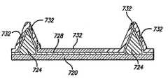
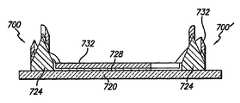
예시적인 나선형 미세 전자 스프링 접속체(100)가 도1에 도시되어 있다. 스프링 접속체(100)는 피라미드형 순응성 패드(110) 형태의 제1 비도전성 탄성 중합체 층, 및 금속 트레이스(102) 형태의 제2 도전성 탄성 층의 두 개의 주요 재료 층을 포함한다. 스프링 접속체(100)는 도전성 층(102; 트레이스)의 적어도 일부가 비도전성 층(110; 패드)을 중첩하고 두 층들이 서로 접속체(100)를 한정하기 때문에, 층상으로 설명된다.An exemplary helical
순응성 패드(110)는 본원에서 설명되는 파라미터 내에서 임의의 적합한 형상일 수 있다. 본 발명의 일 실시예에서, 이는 성형된 형상과 같은 정밀하게 형성된 형상이다. 다른 실시예에서, 패드(110)는 비교적 무정형인 덩어리와 같이, 덜 한정된 형상일 수 있다. 패드의 형태는 패드 표면 위에 적층되는 비교적 강성인 금속 팁 및 비임에 부가될 수 있다. 조밀하게 존재하는 스프링 접속체 어레이를 가로지른 고도의 균일성을 보장하기 위해, 각각의 패드는 패드들 사이의 가변성을 최소화하는 평행 공정을 사용하여 형성될 수 있다. 한꺼번에 성형하는 것과 같은 평행 형성은 개별 덩어리 형성보다 시간을 덜 요구하는 추가의 이점을 제공한다.
특히, 패드(110)는 피라미드 형상을 갖지만, 예를 들어 원추형, 반구형, 절두 원추형과 같은 다른 적합한 형상이 사용될 수 있다. 더욱 일반적으로, 패드(110)는 패드가 기판(116)에 부착되는 상대적으로 크고 편평한 기부 영역(112) 및 기판으로부터 멀리 연장되며 기판으로부터 멀리 있는 상대적으로 작은 단부 영역으로 테이퍼지는 자유 측표면(109)을 갖는 테이퍼진 질량체로서 설명될 수 있다. 단부 영역은 금속 팁(104)을 중첩시킴으로써 도1의 도면으로부터 숨겨져 있다. 이러한 테이퍼진 형상은 한정된 팁 구조물을 효율적으로 지지하면서, 기판(116)에 대한 부착을 위한 영역을 최대화한다. 이러한 실시예에서, 피라미드 형상은 탄성 중합체 재료로부터 탈기에 대한 잠재성을 감소시켜서, 발생할 수 있는 임의의 탈기로부터 접속체(100)를 통기시키고 접속체 어레이를 가로지른 열 응력 경감을 위한 증가된 측방향 가요성을 제공한다.In particular,
피라미드형 순응성 패드는 원하는 테이퍼 특징을 갖는 피라미드 형상이 일반 적으로 이용 가능한 결정성 실리콘 재료의 특성을 이용함으로써 큰 정밀도를 가지고 매우 작은 스케일로 쉽게 형성될 수 있기 때문에, 특히 적합할 수 있다. 실리콘 재료 내의 결정면의 배향에 의해 한정된 측표면을 갖는 피라미드형 피트가 KOH와 같은 적합한 에칭제에 대해 포토레지스트의 적합하게 패턴화된 층으로 덮인 실리콘 기판을 노출시킴으로써 쉽게 제작될 수 있다는 것이 공지되어 있다. 따라서, 실질적으로 동일한 피라미드형 피트의 어레이가 실리콘 기판 내에서 제작될 수 있고, 피트를 갖는 기판은 동일한 피라미드형 순응성 패드의 어레이를 형성하기 위한 주형으로서 사용될 수 있다. 프리즘, 절두 피라미드 또는 프리즘, 및 단차 피라미드 또는 프리즘과 같은 관련 형상이 당업자에게 명백한 바와 같이 적합한 에칭 및 차폐 공정을 사용하여 유사하게 형성될 수 있다.Pyramidal compliant pads are particularly suitable because pyramidal shapes with desired taper characteristics can be easily formed on a very small scale with great precision by utilizing the properties of commonly available crystalline silicon materials. It is known that pyramidal pits having side surfaces defined by the orientation of the crystal planes in the silicon material can be readily fabricated by exposing a silicon substrate covered with a suitably patterned layer of photoresist to a suitable etchant such as KOH. . Thus, arrays of substantially identical pyramidal pits can be fabricated within a silicon substrate, and substrates with pits can be used as a template to form an array of identical pyramidal compliant pads. Related shapes such as prisms, truncated pyramids or prisms, and stepped pyramids or prisms can be similarly formed using suitable etching and shielding processes, as will be apparent to those skilled in the art.
순응성 패드(110)는 임의의 적합한 재료로 제조될 수 있다. 예를 들어, 적합한 탄성 중합체 재료는 실리콘 고무, 천연 고무, 고무화 플라스틱, 및 매우 다양한 다른 유기 중합체 재료를 포함할 수 있다. 당업자는 (온도 또는 화학적 환경과 같은) 의도된 작동 환경 및 스프링 접속체의 원하는 구조적 특징을 고려함으로써 적합한 재료를 선택할 수 있다. 예를 들어, 적합하게 부드러운 탄성 재료는 접속의 기하학적 형상, 원하는 압축성의 범위, 및 최대 접속력이 정의되면 선택될 수 있다. 양호하게는, 패드 재료는 임의의 입자성 충전 재료가 없는 균질 플라스틱 재료이고, 본래 비도전성이다. 균질 플라스틱 재료는 약 5 mil (약 130 ㎛)보다 더 작은 폭의 순응성 패드에 대해, 작은 스케일에서 정밀한 패드 형상으로 더 쉽게 형성될 수 있다.
순응성 패드(110)는 전기적 연결이 필요한 단자(114)로부터 이격된 위치에서 기판(116)에 부착된다. 도전성 트레이스(102)가 그 다음 전기 도금에 의해 단자(114)로부터 순응성 패드의 단부 영역으로 적층된다. 트레이스(102)는 임의의 적합한 금속 또는 금속 합금으로 구성될 수 있고, 하나 이상의 층을 포함할 수 있다. 예를 들어, 트레이스(102)는 도전성을 위해 비교적 얇은 금 층으로 덮인, 강도 및 강성을 위한 니켈 또는 니켈 합금의 비교적 두꺼운 층으로 구성될 수 있다. 트레이스(102)는 양호하게는 패드(110)의 단부 영역 위에 적층된 접속 팁 부분(104), 패드(110)의 기부(112)로부터 접속 팁(104)으로 연장되는 패드 지지형 비임 부분(106), 및 비임 부분(106)을 단자(114)에 연결시키는 기판 지지형 재분배 트레이스 부분(108)을 갖는 금속의 통합편이다. 접속 팁(104)은 정합 단자의 산화 및 오염 층을 관통하기 위해 (도시된 바와 같이) 비교적 뾰족할 수 있다. 대안으로, 접속 팁(104)은 납땜 볼과 같은 특징부를 지지하기 위해 비교적 편평할 수 있다. 비임 부분(106)은 비임 길이를 따라 보다 균일하게 응력을 분포시키는 이점을 제공할 수 있도록 기부(112)에서의 더 큰 폭으로부터 팁(104)에서의 더 좁은 목부로 테이퍼질 수 있다. 대안으로, 비임(106)은 일정한 폭이거나, 임의의 다른 적합한 형상을 가질 수 있다. 기판(116)은 반도체 다이 또는 웨이퍼, 다이 또는 웨이퍼용 커넥터 또는 소켓, 및 인쇄 회로 기판을 포함하지만 그에 제한되지 않는 임의의 적합한 전자 장치일 수 있다.The
스프링 접속체(100)는 도2에 도시된 바와 같이, 피치 확장형 어레이(118) 내에서 쉽게 사용될 수 있다. 기판(116) 상의 단자(114)들은 제1 피치(P1)로 배치되 고, 접속 팁(104)들은 더 넓은 피치(P2)로 배치되고, P2가 P1보다 더 크다.The
본 발명의 실시예에서, 나선형 트레이스는 테이퍼진 나선형 스프링 접속체를 제공하도록 원추형 순응성 패드 주위로 그리고 위로 패턴화될 수 있다. 예를 들어, 기판(306) 상에 배치된 원추형 순응성 패드(304) 주위로 그리고 위로 패턴화된 금속 트레이스(302)를 포함하는 나선형 접속체(300)가 도3에 도시된다. 접속체(300)는 기판의 (도시되지 않은) 단자로부터 순응성 패드의 기부까지 재분배 트레이스(308)를 추가로 포함할 수 있다. 금속 트레이스(302)는 접속체(300)의 원하는 특성에 따라서 순응성 패드(304)와 비교하여 비교적 강성이거나 또는 비교적 유연할 수 있다. 금속 트레이스가 비교적 강성을 가질 경우, 나선 형상은 트레이스(302) 재료에 과응력을 주지 않고 더 큰 범위의 휨을 갖는 스프링 접속체(300)를 제공할 수 있다.In embodiments of the invention, the helical traces may be patterned around and up the conical compliant pad to provide a tapered helical spring contact. For example, a
일부 적용에서, 도4에 도시된 바와 같이 금속 트레이스가 형성된 후 기판(416) 상에 접촉체(400)를 남기면서 순응성 패드를 제거하는 것일 바람직할 수 있다. 다르게는, 접촉체(400)는 비순응성 희생 재료의 적절한 형상의 패드 위로 형성되고, 그후 희생 재료는 제거될 수 있다. 접속체(300)와 마찬가지로, 스프링 접속체(400)는 나선 경로를 따라 기판(416)으로부터 이격되게 연장되는 금속 트레이스(412)를 포함한다. 선택적으로, 스프링 접속체는 재분배 트레이스를 통해 기판(416)의 (도시되지 않은) 단자에 연결될 수 있다. 스프링 접촉체는 (도시된 바와 같은) 원추 나선형 또는 임의의 다른 양호한 나선 패턴으로 형성될 수 있다. 예를 들어, 사각형 나선 접속체는 도1에 도시된 바와 같은 피라미드형 패드 주위로 그리 고 위로 금속 트레이스를 패턴화시킴으로써 형성된다.In some applications, it may be desirable to remove the compliant pad leaving the
도5는 본 발명에 따른 미세 전자 스프링 접속체를 형성하기 위한 방법(500)의 예시적인 단계들을 도시한다. 초기 단계(502)에서, 순응성 패드가 희생 기판 상에 형성된다. 순응성 패드의 어레이를 형성하기 위해, 형성되는 스프링 접속체 어레이 내의 접속 팁의 원하는 배열에 대응하는 패턴의 실리콘 기판과 같은 희생 기판 내에 정밀 피트들이 형성된다. 정밀 피트는 순응성 패드의 원하는 형상에 대응하는 형상으로 형성되고, 예를 들어 피라미드형 피트가 피라미드형 패드 등을 형성하도록 사용된다. 임의의 적합한 방법이 정밀 피트를 형성하기 위해 사용될 수 있고, 특히 다양한 리소그래피/에칭 기술이 다양한 형상의 피트를 형성하기 위해 채용될 수 있다. 피트가 생성된 후에, 희생 기판은 양호하게는 PTFE 재료 또는 다른 불소 중합체와 같은 적합한 이형제의 얇은 층으로 코팅된다. 순응성 패드를 형성하는 다른 방법은 기판 상에 직접 미경화 또는 연화된 탄성 중합체 재료 덩어리를 적층시킨 다음 탄성 중합체를 제 위치에서 경화시키는 것이다.5 shows exemplary steps of a
희생 기판이 준비된 후에, 피트는 양호하게는 액체 상태의 선택된 탄성 중합체 재료로 충전될 수 있다. 접속체들이 형성된 기판("장치 기판")은 그 다음 희생 기판에 장착될 수 있고, 탄성 중합체 재료는 장치 기판이 제 위치에 있을 때 경화되고, 이에 의해 기판에 순응성 패드를 부착시킨다. 기판 및 그의 부착된 패드는 그 다음 희생 기판으로부터 제거되어, 단계(504)에서 지시된 바와 같이 패드를 장치 기판으로 전달한다. 희생 기판은 필요하다면 재사용될 수 있다.After the sacrificial substrate is prepared, the pit can be filled with the selected elastomeric material, preferably in the liquid state. The substrate on which the contacts are formed ("device substrate") may then be mounted to the sacrificial substrate, and the elastomeric material cures when the device substrate is in place, thereby attaching a compliant pad to the substrate. The substrate and its attached pad are then removed from the sacrificial substrate to transfer the pad to the device substrate as indicated in
대안으로, 희생 기판 내의 피트가 액체 탄성 중합체로 충전된 후에, 탄성 중 합체 재료는 희생 기판이 자유롭게 개방되어 있는 채로 경화될 수 있다. 희생 기판은 그 다음 적합한 접착제 재료로 코팅되고, 이에 의해 순응성 패드의 노출된 기부를 코팅한다. 양호하게는, 접착제 재료는 탄성 중합체 재료 위의 영역을 제외하고 희생 기판으로부터 제거될 수 있도록 패턴화될 수 있다. 또한, 접착제 재료는 양호하게는 압력 감응식이어서, 접속체 상에서 정합 기판과 부착된다. 순응성 패드는 그 다음 원하는 대로 장치 기판으로 전달될 수 있다.Alternatively, after the pits in the sacrificial substrate are filled with the liquid elastomer, the elastomeric material can be cured with the sacrificial substrate freely open. The sacrificial substrate is then coated with a suitable adhesive material, thereby coating the exposed base of the compliant pad. Preferably, the adhesive material may be patterned such that it can be removed from the sacrificial substrate except for the area above the elastomeric material. In addition, the adhesive material is preferably pressure sensitive so that it adheres with the mating substrate on the connection. The compliant pad can then be transferred to the device substrate as desired.
순응성 패드가 장치 기판 상에서 제 위치에 있을 때, 단계(506)에서, 도전성 트레이스가 장치 기판의 단자와 순응성 패드의 상부 사이에 배치된다. 도6은 장치 기판 및 순응성 패드 상에 도전성 트레이스를 적층시키기 위한 방법(600)의 예시적인 단계들을 도시한다. 단계(602)에서, 시드 층이 장치 기판 및 그의 부착된 순응성 패드의 전체 표면 위에 적층된다. 한 가지 적합한 시드 층은 스퍼터링된 티타늄-텅스텐 층이고, 적합한 시드 층은 당업자에 의해 선택될 수 있다. 시드 층은 무전해 증착을 포함하는 다른 방법으로 적층될 수 있다.When the compliant pad is in place on the device substrate, at step 506 a conductive trace is disposed between the terminal of the device substrate and the top of the compliant pad. 6 illustrates exemplary steps of a
단계(604)에서, 희생 층이 시드 층 위에 적층된다. 희생 층은 포토레지스트 재료와 같은 패턴화될 수 있는 재료이고, 양호하게는 장치 기판 및 그의 돌출된 탄성 중합체 패드 위에 고도의 콘포멀 층으로서 도포된다. 레지스트 재료의 콘포멀 층을 적층시키기 위해 다양한 방법이 사용될 수 있다. 약 35 ㎛까지의 두께에 대한 한 가지 적합한 코팅은 전착(전기 영동 레지스트)이다. 다른 방법은 분사 코팅, 스핀 코팅, 또는 코팅 재료의 층류 유동이 장치 기판 위로 통과되는 메니스커스 코팅을 포함할 수 있다. 더 큰 깊이는 재료의 층을 연속적으로 코팅 및 경화시 킴으로써 축적될 수 있다. 희생 층의 최소 깊이는 양호하게는 적층되는 금속 트레이스의 원하는 두께보다 크거나 같다.In
단계(606)에서, 희생 층은 도전성 트레이스가 적층되어야 하는 영역 내의 시드 층을 노출시키도록 패턴화된다. 통상, 패턴화는 기술 분야에 공지된 임의의 적합한 광 패턴화 기술을 사용하여 달성될 수 있다. 단계(608)에서, 도전성 트레이스 재료는 전기 도금에 의해 시드 층의 노출된 영역 위에 원하는 깊이로 적층된다. 니켈 또는 니켈 합금의 비교적 두꺼운 층과, 이후의 금의 비교적 얇은 층과 같은 다른 재료들의 연속된 층들이 원하는 대로 도포될 수 있다. 단계(610)에서, 희생 층은 적합한 용제 내에서 용해되어 제거된다. 장치는 이에 의해 본 발명에 따른 스프링 접속체의 어레이를 구비한다.In
금속 트레이스가 비교적 얇고 가요성이어야 하는 스프링 접속체에 대해, 금속 트레이스는 전기 도금에 의해 적층될 필요가 없고, 양호하게는 스퍼터링 또는 증착과 같은 방법에 의해 적층될 수 있다. 그러한 경우에, 장치 기판 및 순응성 패드의 전체 표면은 시드 층에서와 같이, 금속의 얇은 층 또는 층들에 의해 원하는 깊이로 코팅될 수 있다. 그 다음, 포토레지스트 층이 도포되어 금속 트레이스 층이 요구되는 장치 기판의 영역을 보호하도록 패턴화될 수 있고, 금속 층의 잔여 비보호 영역은 에칭 단계에서 제거된다. 전기 도금 단계를 제거함으로써, 처리 시간이 비교적 강성인 금속 접속 소자를 요구하지 않는 용도에 대해 실질적으로 감소될 수 있다.For spring contacts where the metal traces should be relatively thin and flexible, the metal traces do not need to be laminated by electroplating, and may preferably be deposited by methods such as sputtering or deposition. In such a case, the entire surface of the device substrate and the compliant pad can be coated to a desired depth by a thin layer or layers of metal, such as in the seed layer. A photoresist layer can then be applied and patterned to protect the area of the device substrate where the metal trace layer is desired, and the remaining unprotected areas of the metal layer are removed in the etching step. By eliminating the electroplating step, processing time can be substantially reduced for applications that do not require relatively rigid metal connection elements.
나선형 스프링 접속체를 형성하는 하나의 적절한 방법(500, 600)이 도7a 내 지 도7f를 참조하여 기술된다. 도7a는 사실상 균일한 두께의 층일 수 있는 순응성 재료의 층(722)으로 덮여지는 반도체 웨이퍼, 세라믹 타일 또는 탐침 카드와 같은 기부 기판(720)의 단면도를 도시한다. 층(722)을 위한 순응성 재료는 순응성 재료를 형성하기 위해 여기에 언급된 탄성중합체 재료들 중 하나와 같은 임의의 적절한 성형 가능 재료, 또는 경화될 때 순응성을 갖는 지의 여부에 관계없이 포토레지스트 재료와 같은 임의의 성형 가능 재료일 수 있다.One
층(722)은 층(722) 내로 엠보싱 공구를 가압하는 것과 같이 하나 이상의 패드 또는 돌출부(724)를 제공하도록 성형 또는 형성될 수 있다. 엠보싱 공구는 잔여 층(726)을 남기고, 이는 플라즈마 등방성 에칭과 같은 임의의 적절한 공정을 사용하여 제거될 수 있다. 이와 달리, 패드(724)는 상술한 바와 같은 액체 수지를 사용하여 성형되거나, 에칭 또는 층(722)에서 적절한 형태로 재료를 제거함으로써 제공될 수 있다. 패드(724)는 임의의 특정 치수로 되지는 않음을 알아야 한다. 일반적으로, 도7a 내지 도7f의 수직 치수는 명백하지 않을 수 있는 특징을 도시하기 위해 기판(720)의 통상의 두께에 비해 과장되었다.
시드 층(728)은 스퍼터링과 같은 방법으로 기판(720) 및 패드(724) 위에 적층될 수 있다. 그후, 포토레지스트 층과 같은 희생 층(730)이 시드 층 위에 적층되어 도7c에 도시된 것과 같은 구조를 남기게 된다. 그후, 층(730)은 두꺼운 층의 금속 재료를 적층하기에 바람직한 영역에 시드 층(728)이 보이도록 패턴화된다. 패턴화 후의 층(730)의 모습이 도7d에 도시된다. 그후, 도전성 재료(732)가 전기도금과 같은 공정을 사용하여 노출된 시드 층(728) 위로 적층될 수 있다. 상술한 바와 같은 니켈 또는 니켈 합금과 같은 임의의 적절한 도전성 재료가 사용될 수 있다. 시드 층 위로 도금된 도전성 재료(732)를 갖는 희생 층(730)의 모습이 도7e에 도시된다.
그후, 도7f에 도시된 바와 같이 희생 층(730)은 기술 분야에 알려진 바와 같이 제거되어 하나 이상의 스프링 접속체(700, 700')를 제공하게 된다. 패드(724)는 상술한 바와 같은 순응성 패드일 수 있다. 이와 달리, 패드(724)는 도8(측면도)에 도시된 바와 같은 자립형 접속체(800, 800')를 제공하도록 기판(720)으로부터 벗겨질 수 있다. 유사한 접속체(400)의 사시도가 도4에 도시된다.Thereafter, as shown in FIG. 7F, the
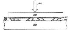
도9는 표면 상에 나선형 미세 전자 스프링 접속체(800)의 어레이를 갖는 예시적인 플립-칩 장치(900)의 확대된 평면도를 도시한다. 각각의 접속체(800)는 장치의 단자(914)에 연결된다. 장치(900)는 메모리 칩 또는 마이크로 프로세서와 같은 반도체 장치일 수 있다. 스프링 접속체(800)는 양호하게는 반도체 웨이퍼로부터의 개별화 이전에 장치(900) 상에 직접 형성된다. 접속체(800)는 그 다음 테스트 및 조립을 목적으로 장치에 연결되도록 사용될 수 있다. 플립-칩 장착이 더 콤팩트한 설계를 나타내지만, 접속체(800)는 필요하다면 CSP 설계 내로 유사하게 통합될 수 있다는 것을 이해해야 한다.9 shows an enlarged plan view of an exemplary flip-
도10은 인쇄 회로 기판과 같은 정합 전기 부품(954)과 접속된 장치(900)의 측면도를 도시한다. 각각의 접속체(800)의 접속 팁이 부품(950)의 단자(952)와 접속한다. 장치(900)의 설치를 쉽게 탈착 가능하도록 만들도록 요구되면, 제어된 양의 압축력(910)이 장착 프레임 또는 다른 체결 장치를 사용하여 인가될 수 있다. 압축력(910)은 기판(950)에 대해 직교하는 방향 및 기판(950)에 대해 평행한 측방향으로의 접속체(800)의 변형을 일으킨다. 접속체(800)의 측방향 변형은 접속 팁에서 유익한 와이핑 작용을 제공할 수 있다. 장치(900)는 압축력(910)을 해제함으로써 원하는 대로 탈착될 수 있다. 접속체(800)가 단자(952)에 납땜되지 않으면, 기판(950)과 장치(900) 사이의 열 부정합으로부터의 측방향 응력은 접속체(800)의 접속 팁과 단자(952) 사이의 활주에 의해 경감될 수 있다.10 shows a side view of an
나선형 미세 전자 접속체의 양호한 실시예를 이렇게 설명했지만, 내부 시스템의 몇몇 장점이 달성되었다는 것은 당업자에게 명백하다. 또한, 그의 다양한 변형, 적응 및 변경이 본 발명의 범주 및 취지 내에서 이루어질 수 있다는 것을 이해해야 한다. 예를 들어, 순응성 패드 및 스프링 접속체의 특정 형상이 도시되었지만, 전술한 본 발명의 개념은 여기서 설명된 일반적인 특성을 갖는 패드 및 금속 소자의 다른 형상 및 구성에 동일하게 적용될 수 있다는 것이 명백하다.While the preferred embodiment of the helical microelectronic connectors has been described in this way, it is apparent to those skilled in the art that several advantages of the internal system have been achieved. In addition, it should be understood that various modifications, adaptations, and changes may be made within the scope and spirit of the invention. For example, although specific shapes of compliant pads and spring contacts are shown, it is clear that the concepts of the present invention described above may equally apply to other shapes and configurations of pads and metal elements having the general characteristics described herein.
다른 예로서, 본원에서 설명된 스프링 접속체는 반도체 장치뿐만 아니라 (제한적이지 않게) 탐침 카드 및 다른 테스트 장치를 포함한 임의의 전자 부품과 함께 사용될 수 있다. 또 다른 예로서, 스프링 접속 구조물의 강도, 탄성, 도전성 등을 향상시키는 재료와 같은 추가의 재료가 전술한 스프링 접속 구조물 상에 적층될 수 있다. 또 다른 예로서, 하나 이상의 재료 층이 전술한 바와 같이 스프링 접속 구조물을 생성하기 전에 또는 그 후에 전자 부품 상에 형성될 수 있다. 예를 들어, (절연 층에 의해 분리된) 하나 이상의 재분배 트레이스의 층이 전자 부품 상에 형성되고 이후에 재분배 층 상에 스프링 접속체를 형성할 수 있다. 다른 예로서, 스 프링 접속체가 먼저 형성되고 이후에 하나 이상의 재분배 트레이스의 층을 형성할 수 있다. 다른 예로서, 스프링 접속체가 먼저 형성된 후, 하나 이상의 재분배 트레이스가 형성될 수 있다.As another example, the spring contacts described herein can be used with any electronic component, including but not limited to probe cards and other test devices, as well as semiconductor devices. As another example, additional materials, such as materials that enhance the strength, elasticity, conductivity, and the like of the spring connection structure, may be laminated on the aforementioned spring connection structure. As another example, one or more layers of material may be formed on the electronic component before or after creating the spring contact structure as described above. For example, a layer of one or more redistribution traces (separated by an insulating layer) may be formed on the electronic component and then form spring contacts on the redistribution layer. As another example, a spring contact can be formed first and then a layer of one or more redistribution traces. As another example, a spring contact may be formed first, followed by one or more redistribution traces.
Claims (20)
Translated fromKoreanApplications Claiming Priority (2)
| Application Number | Priority Date | Filing Date | Title |
|---|---|---|---|
| US10/411,175 | 2003-04-10 | ||
| US10/411,175US6948940B2 (en) | 2003-04-10 | 2003-04-10 | Helical microelectronic contact and method for fabricating same |
Publications (1)
| Publication Number | Publication Date |
|---|---|
| KR20060002954Atrue KR20060002954A (en) | 2006-01-09 |
Family
ID=33130922
Family Applications (1)
| Application Number | Title | Priority Date | Filing Date |
|---|---|---|---|
| KR1020057019080ACeasedKR20060002954A (en) | 2003-04-10 | 2004-04-12 | Helical microelectronic contact and method for fabricating same |
Country Status (7)
| Country | Link |
|---|---|
| US (2) | US6948940B2 (en) |
| EP (1) | EP1616352A1 (en) |
| JP (1) | JP2006523040A (en) |
| KR (1) | KR20060002954A (en) |
| CN (1) | CN1894792A (en) |
| TW (1) | TWI338351B (en) |
| WO (1) | WO2004093189A1 (en) |
Cited By (2)
| Publication number | Priority date | Publication date | Assignee | Title |
|---|---|---|---|---|
| KR100784753B1 (en)* | 2006-09-27 | 2007-12-13 | (주)넴스프로브 | Method for manufacturing connector using 3D photolithography |
| KR100852514B1 (en)* | 2006-07-31 | 2008-08-18 | 한국과학기술연구원 | Perpendicular Type Probe for Test of Semiconductor, Probe Card with the Probes and Methods for Manufacturing the Probe Card |
Families Citing this family (50)
| Publication number | Priority date | Publication date | Assignee | Title |
|---|---|---|---|---|
| US8033838B2 (en) | 1996-02-21 | 2011-10-11 | Formfactor, Inc. | Microelectronic contact structure |
| SE522031C2 (en)* | 2001-07-12 | 2004-01-07 | Perlos Ab | Two-component antenna and method of making such |
| US20060051948A1 (en)* | 2003-02-04 | 2006-03-09 | Microfabrica Inc. | Microprobe tips and methods for making |
| US7412767B2 (en)* | 2003-02-04 | 2008-08-19 | Microfabrica, Inc. | Microprobe tips and methods for making |
| US7363705B2 (en)* | 2003-02-04 | 2008-04-29 | Microfabrica, Inc. | Method of making a contact |
| US20060053625A1 (en)* | 2002-05-07 | 2006-03-16 | Microfabrica Inc. | Microprobe tips and methods for making |
| US7273812B2 (en)* | 2002-05-07 | 2007-09-25 | Microfabrica Inc. | Microprobe tips and methods for making |
| US7265565B2 (en) | 2003-02-04 | 2007-09-04 | Microfabrica Inc. | Cantilever microprobes for contacting electronic components and methods for making such probes |
| US7241689B2 (en)* | 2003-02-04 | 2007-07-10 | Microfabrica Inc. | Microprobe tips and methods for making |
| US10416192B2 (en) | 2003-02-04 | 2019-09-17 | Microfabrica Inc. | Cantilever microprobes for contacting electronic components |
| US20080211524A1 (en)* | 2003-02-04 | 2008-09-04 | Microfabrica Inc. | Electrochemically Fabricated Microprobes |
| US6948940B2 (en)* | 2003-04-10 | 2005-09-27 | Formfactor, Inc. | Helical microelectronic contact and method for fabricating same |
| US7114961B2 (en)* | 2003-04-11 | 2006-10-03 | Neoconix, Inc. | Electrical connector on a flexible carrier |
| US20080108221A1 (en)* | 2003-12-31 | 2008-05-08 | Microfabrica Inc. | Microprobe Tips and Methods for Making |
| DE102004019588A1 (en)* | 2004-04-22 | 2005-11-17 | Osram Opto Semiconductors Gmbh | Process for structuring at least one layer and electrical component with structures from the layer |
| DE102004030140B3 (en)* | 2004-06-22 | 2006-01-19 | Infineon Technologies Ag | Flexible contacting device |
| US7688095B2 (en)* | 2004-07-30 | 2010-03-30 | International Business Machines Corporation | Interposer structures and methods of manufacturing the same |
| US7771208B2 (en) | 2004-12-16 | 2010-08-10 | International Business Machines Corporation | Metalized elastomeric electrical contacts |
| CN101288205B (en)* | 2004-12-16 | 2011-09-21 | 国际商业机器公司 | Metallized Elastomer Electrical Contacts |
| US7316572B2 (en)* | 2005-02-03 | 2008-01-08 | International Business Machines Corporation | Compliant electrical contacts |
| JP2006261565A (en)* | 2005-03-18 | 2006-09-28 | Alps Electric Co Ltd | Electronic functional component mounted body and its manufacturing method |
| US7790987B2 (en)* | 2005-04-27 | 2010-09-07 | Sony Computer Entertainment Inc. | Methods and apparatus for interconnecting a ball grid array to a printed circuit board |
| JP2008039502A (en)* | 2006-08-03 | 2008-02-21 | Alps Electric Co Ltd | Contact and its manufacturing method |
| JP2008060510A (en)* | 2006-09-04 | 2008-03-13 | Alps Electric Co Ltd | Method for manufacturing semiconductor chip mounted circuit and mounted circuit therefor |
| US7674112B2 (en)* | 2006-12-28 | 2010-03-09 | Formfactor, Inc. | Resilient contact element and methods of fabrication |
| US7585173B2 (en)* | 2007-03-30 | 2009-09-08 | Tyco Electronics Corporation | Elastomeric electrical contact |
| US8832936B2 (en)* | 2007-04-30 | 2014-09-16 | International Business Machines Corporation | Method of forming metallized elastomeric electrical contacts |
| JP2008281519A (en)* | 2007-05-14 | 2008-11-20 | Alps Electric Co Ltd | Probe card and its manufacturing method |
| TW200922009A (en)* | 2007-12-07 | 2009-05-16 | Jye Chuang Electronic Co Ltd | Contact terminal |
| KR101004911B1 (en)* | 2008-08-12 | 2010-12-28 | 삼성전기주식회사 | Manufacturing method of micro electromechanical parts |
| US8278748B2 (en) | 2010-02-17 | 2012-10-02 | Maxim Integrated Products, Inc. | Wafer-level packaged device having self-assembled resilient leads |
| EP2543051B1 (en)* | 2010-03-03 | 2017-09-06 | Philips Lighting Holding B.V. | Kit of parts, connection device, lighting device and luminaire |
| US8686560B2 (en) | 2010-04-07 | 2014-04-01 | Maxim Integrated Products, Inc. | Wafer-level chip-scale package device having bump assemblies configured to mitigate failures due to stress |
| WO2014193406A1 (en)* | 2013-05-31 | 2014-12-04 | Hewlett-Packard Development Company, L.P. | Modifying a base layer of an object |
| CN104370272B (en)* | 2014-10-30 | 2016-07-06 | 无锡微奥科技有限公司 | A kind of MEMS autoregistration height comb and manufacture method thereof |
| US9717148B2 (en)* | 2015-09-18 | 2017-07-25 | Quartzdyne, Inc. | Methods of forming a microelectronic device structure, and related microelectronic device structures and microelectronic devices |
| JP6805690B2 (en)* | 2016-09-30 | 2020-12-23 | セイコーエプソン株式会社 | A method for manufacturing a MEMS device, a liquid injection head, a liquid injection device, and a MEMS device. |
| US11262383B1 (en) | 2018-09-26 | 2022-03-01 | Microfabrica Inc. | Probes having improved mechanical and/or electrical properties for making contact between electronic circuit elements and methods for making |
| US11973301B2 (en) | 2018-09-26 | 2024-04-30 | Microfabrica Inc. | Probes having improved mechanical and/or electrical properties for making contact between electronic circuit elements and methods for making |
| US12078657B2 (en) | 2019-12-31 | 2024-09-03 | Microfabrica Inc. | Compliant pin probes with extension springs, methods for making, and methods for using |
| US12181493B2 (en) | 2018-10-26 | 2024-12-31 | Microfabrica Inc. | Compliant probes including dual independently operable probe contact elements including at least one flat extension spring, methods for making, and methods for using |
| US12000865B2 (en) | 2019-02-14 | 2024-06-04 | Microfabrica Inc. | Multi-beam vertical probes with independent arms formed of a high conductivity metal for enhancing current carrying capacity and methods for making such probes |
| US12196782B2 (en) | 2019-12-31 | 2025-01-14 | Microfabrica Inc. | Probes with planar unbiased spring elements for electronic component contact, methods for making such probes, and methods for using such probes |
| US11761982B1 (en) | 2019-12-31 | 2023-09-19 | Microfabrica Inc. | Probes with planar unbiased spring elements for electronic component contact and methods for making such probes |
| US11802891B1 (en) | 2019-12-31 | 2023-10-31 | Microfabrica Inc. | Compliant pin probes with multiple spring segments and compression spring deflection stabilization structures, methods for making, and methods for using |
| US12196781B2 (en) | 2019-12-31 | 2025-01-14 | Microfabrica Inc. | Probes with planar unbiased spring elements for electronic component contact, methods for making such probes, and methods for using such probes |
| US10937752B1 (en)* | 2020-08-03 | 2021-03-02 | Topline Corporation | Lead free solder columns and methods for making same |
| US11774467B1 (en) | 2020-09-01 | 2023-10-03 | Microfabrica Inc. | Method of in situ modulation of structural material properties and/or template shape |
| US12146898B2 (en) | 2020-10-02 | 2024-11-19 | Microfabrica Inc. | Multi-beam probes with decoupled structural and current carrying beams and methods of making |
| FR3119048A1 (en)* | 2021-01-21 | 2022-07-22 | Commissariat A L'energie Atomique Et Aux Energies Alternatives | INTERCONNECTION WITH AME |
Family Cites Families (32)
| Publication number | Priority date | Publication date | Assignee | Title |
|---|---|---|---|---|
| US3881799A (en)* | 1972-09-11 | 1975-05-06 | George H Elliott | Resilient multi-micro point metallic junction |
| US4466184A (en)* | 1981-04-21 | 1984-08-21 | General Dynamics, Pomona Division | Method of making pressure point contact system |
| US5829128A (en)* | 1993-11-16 | 1998-11-03 | Formfactor, Inc. | Method of mounting resilient contact structures to semiconductor devices |
| US5917707A (en)* | 1993-11-16 | 1999-06-29 | Formfactor, Inc. | Flexible contact structure with an electrically conductive shell |
| US5225771A (en)* | 1988-05-16 | 1993-07-06 | Dri Technology Corp. | Making and testing an integrated circuit using high density probe points |
| DE3838413A1 (en)* | 1988-11-12 | 1990-05-17 | Mania Gmbh | ADAPTER FOR ELECTRONIC TEST DEVICES FOR PCBS AND THE LIKE |
| US5090118A (en)* | 1990-07-31 | 1992-02-25 | Texas Instruments Incorporated | High performance test head and method of making |
| US5187020A (en)* | 1990-07-31 | 1993-02-16 | Texas Instruments Incorporated | Compliant contact pad |
| US5092782A (en)* | 1991-02-01 | 1992-03-03 | Beaman Brian S | Integral elastomeric card edge connector |
| US5172050A (en)* | 1991-02-15 | 1992-12-15 | Motorola, Inc. | Micromachined semiconductor probe card |
| US5177438A (en)* | 1991-08-02 | 1993-01-05 | Motorola, Inc. | Low resistance probe for semiconductor |
| JPH0618555A (en) | 1992-06-30 | 1994-01-25 | Meisei Denshi Kogyo Kk | Microspring contact, its aggregate, terminal for electric connection composed of the aggregate and production of microspring contact |
| JP3345948B2 (en) | 1993-03-16 | 2002-11-18 | ジェイエスアール株式会社 | Method of manufacturing probe head |
| DE4310349C2 (en)* | 1993-03-30 | 2000-11-16 | Inst Mikrotechnik Mainz Gmbh | Sensor head and method for its production |
| JPH0782027B2 (en) | 1993-04-30 | 1995-09-06 | フレッシュクエストコーポレーション | Manufacturing method of test contact pin |
| US5802699A (en)* | 1994-06-07 | 1998-09-08 | Tessera, Inc. | Methods of assembling microelectronic assembly with socket for engaging bump leads |
| JPH07333232A (en) | 1994-06-13 | 1995-12-22 | Canon Inc | Method for forming cantilever having probe |
| US6499216B1 (en)* | 1994-07-07 | 2002-12-31 | Tessera, Inc. | Methods and structures for electronic probing arrays |
| US5476818A (en)* | 1994-08-19 | 1995-12-19 | Motorola, Inc. | Semiconductor structure and method of manufacture |
| US5971253A (en)* | 1995-07-31 | 1999-10-26 | Tessera, Inc. | Microelectronic component mounting with deformable shell terminals |
| JP2934202B2 (en)* | 1997-03-06 | 1999-08-16 | 山一電機株式会社 | Method for forming conductive bumps on wiring board |
| US6059982A (en)* | 1997-09-30 | 2000-05-09 | International Business Machines Corporation | Micro probe assembly and method of fabrication |
| US6031282A (en)* | 1998-08-27 | 2000-02-29 | Advantest Corp. | High performance integrated circuit chip package |
| JP4514855B2 (en)* | 1999-08-19 | 2010-07-28 | 東京エレクトロン株式会社 | Probing card manufacturing method |
| DE10016132A1 (en)* | 2000-03-31 | 2001-10-18 | Infineon Technologies Ag | Electronic component with flexible contact points and method for its production |
| JP3440243B2 (en)* | 2000-09-26 | 2003-08-25 | 株式会社アドバンストシステムズジャパン | Spiral contactor |
| US6439894B1 (en)* | 2001-01-31 | 2002-08-27 | High Connection Density, Inc. | Contact assembly for land grid array interposer or electrical connector |
| US6627092B2 (en)* | 2001-07-27 | 2003-09-30 | Hewlett-Packard Development Company, L.P. | Method for the fabrication of electrical contacts |
| JP4210049B2 (en)* | 2001-09-04 | 2009-01-14 | 株式会社アドバンストシステムズジャパン | Spiral contact |
| JP3814231B2 (en)* | 2002-06-10 | 2006-08-23 | 株式会社アドバンストシステムズジャパン | Spiral contactor and manufacturing method thereof, semiconductor inspection apparatus using the same, and electronic component |
| DE10239080A1 (en)* | 2002-08-26 | 2004-03-11 | Infineon Technologies Ag | Integrated circuit used in wafer level packages comprises an elastically deformable protrusion, a contact unit, and a rewiring unit for electrically connecting an active semiconductor section of the circuit to the contact unit |
| US6948940B2 (en)* | 2003-04-10 | 2005-09-27 | Formfactor, Inc. | Helical microelectronic contact and method for fabricating same |
- 2003
- 2003-04-10USUS10/411,175patent/US6948940B2/ennot_activeExpired - Fee Related
- 2004
- 2004-04-09TWTW093109969Apatent/TWI338351B/ennot_activeIP Right Cessation
- 2004-04-12WOPCT/US2004/011115patent/WO2004093189A1/enactiveApplication Filing
- 2004-04-12EPEP04759412Apatent/EP1616352A1/ennot_activeWithdrawn
- 2004-04-12JPJP2006509899Apatent/JP2006523040A/enactivePending
- 2004-04-12KRKR1020057019080Apatent/KR20060002954A/ennot_activeCeased
- 2004-04-12CNCNA2004800123699Apatent/CN1894792A/enactivePending
- 2005
- 2005-09-27USUS11/237,091patent/US7131848B2/ennot_activeExpired - Fee Related
Cited By (2)
| Publication number | Priority date | Publication date | Assignee | Title |
|---|---|---|---|---|
| KR100852514B1 (en)* | 2006-07-31 | 2008-08-18 | 한국과학기술연구원 | Perpendicular Type Probe for Test of Semiconductor, Probe Card with the Probes and Methods for Manufacturing the Probe Card |
| KR100784753B1 (en)* | 2006-09-27 | 2007-12-13 | (주)넴스프로브 | Method for manufacturing connector using 3D photolithography |
Also Published As
| Publication number | Publication date |
|---|---|
| CN1894792A (en) | 2007-01-10 |
| US7131848B2 (en) | 2006-11-07 |
| US20060024989A1 (en) | 2006-02-02 |
| JP2006523040A (en) | 2006-10-05 |
| TW200503205A (en) | 2005-01-16 |
| WO2004093189A1 (en) | 2004-10-28 |
| US20040203262A1 (en) | 2004-10-14 |
| US6948940B2 (en) | 2005-09-27 |
| EP1616352A1 (en) | 2006-01-18 |
| TWI338351B (en) | 2011-03-01 |
Similar Documents
| Publication | Publication Date | Title |
|---|---|---|
| US6948940B2 (en) | Helical microelectronic contact and method for fabricating same | |
| KR100891066B1 (en) | Microelectronic contact, method for fabricating microelectronic contact, semiconductor device and contact structure | |
| US6007349A (en) | Flexible contact post and post socket and associated methods therefor | |
| JP5306224B2 (en) | Compliance microelectronic assembly and method therefor | |
| US8213184B2 (en) | Method of testing using a temporary chip attach carrier | |
| JP4092361B2 (en) | Semiconductor package assembly | |
| US5810607A (en) | Interconnector with contact pads having enhanced durability | |
| US6948941B2 (en) | Interconnect assemblies and methods | |
| CN102646913B (en) | Making method for electric connector | |
| KR101145886B1 (en) | Electical connection device and test socket having the electrical connection device | |
| US20070054515A1 (en) | Method for fabricating a contact grid array | |
| KR20120112879A (en) | Method to build a wirebond probe card in a many at a time fashion | |
| KR101267651B1 (en) | Microelectronic assemblies having compliancy | |
| US20110043238A1 (en) | Method of manufacturing needle for probe card using fine processing technology, needle manufactured by the method and probe card comprising the needle | |
| US20030080425A1 (en) | Compliant relief wafer level packaging |
Legal Events
| Date | Code | Title | Description |
|---|---|---|---|
| PA0105 | International application | Patent event date:20051007 Patent event code:PA01051R01D Comment text:International Patent Application | |
| PG1501 | Laying open of application | ||
| A201 | Request for examination | ||
| PA0201 | Request for examination | Patent event code:PA02012R01D Patent event date:20071025 Comment text:Request for Examination of Application | |
| E902 | Notification of reason for refusal | ||
| PE0902 | Notice of grounds for rejection | Comment text:Notification of reason for refusal Patent event date:20090428 Patent event code:PE09021S01D | |
| E601 | Decision to refuse application | ||
| PE0601 | Decision on rejection of patent | Patent event date:20091110 Comment text:Decision to Refuse Application Patent event code:PE06012S01D Patent event date:20090428 Comment text:Notification of reason for refusal Patent event code:PE06011S01I |