KR102833377B1 - Light-emitting substrates and display devices - Google Patents
Light-emitting substrates and display devicesDownload PDFInfo
- Publication number
- KR102833377B1 KR102833377B1KR1020227017959AKR20227017959AKR102833377B1KR 102833377 B1KR102833377 B1KR 102833377B1KR 1020227017959 AKR1020227017959 AKR 1020227017959AKR 20227017959 AKR20227017959 AKR 20227017959AKR 102833377 B1KR102833377 B1KR 102833377B1
- Authority
- KR
- South Korea
- Prior art keywords
- light
- voltage
- emitting
- lines
- row
- Prior art date
- Legal status (The legal status is an assumption and is not a legal conclusion. Google has not performed a legal analysis and makes no representation as to the accuracy of the status listed.)
- Active
Links
Images


Classifications
- H—ELECTRICITY
- H10—SEMICONDUCTOR DEVICES; ELECTRIC SOLID-STATE DEVICES NOT OTHERWISE PROVIDED FOR
- H10D—INORGANIC ELECTRIC SEMICONDUCTOR DEVICES
- H10D86/00—Integrated devices formed in or on insulating or conducting substrates, e.g. formed in silicon-on-insulator [SOI] substrates or on stainless steel or glass substrates
- H10D86/40—Integrated devices formed in or on insulating or conducting substrates, e.g. formed in silicon-on-insulator [SOI] substrates or on stainless steel or glass substrates characterised by multiple TFTs
- H10D86/60—Integrated devices formed in or on insulating or conducting substrates, e.g. formed in silicon-on-insulator [SOI] substrates or on stainless steel or glass substrates characterised by multiple TFTs wherein the TFTs are in active matrices
- G—PHYSICS
- G02—OPTICS
- G02F—OPTICAL DEVICES OR ARRANGEMENTS FOR THE CONTROL OF LIGHT BY MODIFICATION OF THE OPTICAL PROPERTIES OF THE MEDIA OF THE ELEMENTS INVOLVED THEREIN; NON-LINEAR OPTICS; FREQUENCY-CHANGING OF LIGHT; OPTICAL LOGIC ELEMENTS; OPTICAL ANALOGUE/DIGITAL CONVERTERS
- G02F1/00—Devices or arrangements for the control of the intensity, colour, phase, polarisation or direction of light arriving from an independent light source, e.g. switching, gating or modulating; Non-linear optics
- G02F1/01—Devices or arrangements for the control of the intensity, colour, phase, polarisation or direction of light arriving from an independent light source, e.g. switching, gating or modulating; Non-linear optics for the control of the intensity, phase, polarisation or colour
- G02F1/13—Devices or arrangements for the control of the intensity, colour, phase, polarisation or direction of light arriving from an independent light source, e.g. switching, gating or modulating; Non-linear optics for the control of the intensity, phase, polarisation or colour based on liquid crystals, e.g. single liquid crystal display cells
- G02F1/133—Constructional arrangements; Operation of liquid crystal cells; Circuit arrangements
- G02F1/1333—Constructional arrangements; Manufacturing methods
- G02F1/1335—Structural association of cells with optical devices, e.g. polarisers or reflectors
- G02F1/1336—Illuminating devices
- G02F1/133602—Direct backlight
- G02F1/133603—Direct backlight with LEDs
- G—PHYSICS
- G02—OPTICS
- G02F—OPTICAL DEVICES OR ARRANGEMENTS FOR THE CONTROL OF LIGHT BY MODIFICATION OF THE OPTICAL PROPERTIES OF THE MEDIA OF THE ELEMENTS INVOLVED THEREIN; NON-LINEAR OPTICS; FREQUENCY-CHANGING OF LIGHT; OPTICAL LOGIC ELEMENTS; OPTICAL ANALOGUE/DIGITAL CONVERTERS
- G02F1/00—Devices or arrangements for the control of the intensity, colour, phase, polarisation or direction of light arriving from an independent light source, e.g. switching, gating or modulating; Non-linear optics
- G02F1/01—Devices or arrangements for the control of the intensity, colour, phase, polarisation or direction of light arriving from an independent light source, e.g. switching, gating or modulating; Non-linear optics for the control of the intensity, phase, polarisation or colour
- G02F1/13—Devices or arrangements for the control of the intensity, colour, phase, polarisation or direction of light arriving from an independent light source, e.g. switching, gating or modulating; Non-linear optics for the control of the intensity, phase, polarisation or colour based on liquid crystals, e.g. single liquid crystal display cells
- G02F1/133—Constructional arrangements; Operation of liquid crystal cells; Circuit arrangements
- G02F1/1333—Constructional arrangements; Manufacturing methods
- G02F1/1335—Structural association of cells with optical devices, e.g. polarisers or reflectors
- G02F1/1336—Illuminating devices
- G02F1/133602—Direct backlight
- G02F1/133612—Electrical details
- G—PHYSICS
- G09—EDUCATION; CRYPTOGRAPHY; DISPLAY; ADVERTISING; SEALS
- G09G—ARRANGEMENTS OR CIRCUITS FOR CONTROL OF INDICATING DEVICES USING STATIC MEANS TO PRESENT VARIABLE INFORMATION
- G09G3/00—Control arrangements or circuits, of interest only in connection with visual indicators other than cathode-ray tubes
- G09G3/20—Control arrangements or circuits, of interest only in connection with visual indicators other than cathode-ray tubes for presentation of an assembly of a number of characters, e.g. a page, by composing the assembly by combination of individual elements arranged in a matrix no fixed position being assigned to or needed to be assigned to the individual characters or partial characters
- G09G3/22—Control arrangements or circuits, of interest only in connection with visual indicators other than cathode-ray tubes for presentation of an assembly of a number of characters, e.g. a page, by composing the assembly by combination of individual elements arranged in a matrix no fixed position being assigned to or needed to be assigned to the individual characters or partial characters using controlled light sources
- G09G3/30—Control arrangements or circuits, of interest only in connection with visual indicators other than cathode-ray tubes for presentation of an assembly of a number of characters, e.g. a page, by composing the assembly by combination of individual elements arranged in a matrix no fixed position being assigned to or needed to be assigned to the individual characters or partial characters using controlled light sources using electroluminescent panels
- G09G3/32—Control arrangements or circuits, of interest only in connection with visual indicators other than cathode-ray tubes for presentation of an assembly of a number of characters, e.g. a page, by composing the assembly by combination of individual elements arranged in a matrix no fixed position being assigned to or needed to be assigned to the individual characters or partial characters using controlled light sources using electroluminescent panels semiconductive, e.g. using light-emitting diodes [LED]
- G09G3/3208—Control arrangements or circuits, of interest only in connection with visual indicators other than cathode-ray tubes for presentation of an assembly of a number of characters, e.g. a page, by composing the assembly by combination of individual elements arranged in a matrix no fixed position being assigned to or needed to be assigned to the individual characters or partial characters using controlled light sources using electroluminescent panels semiconductive, e.g. using light-emitting diodes [LED] organic, e.g. using organic light-emitting diodes [OLED]
- G09G3/3225—Control arrangements or circuits, of interest only in connection with visual indicators other than cathode-ray tubes for presentation of an assembly of a number of characters, e.g. a page, by composing the assembly by combination of individual elements arranged in a matrix no fixed position being assigned to or needed to be assigned to the individual characters or partial characters using controlled light sources using electroluminescent panels semiconductive, e.g. using light-emitting diodes [LED] organic, e.g. using organic light-emitting diodes [OLED] using an active matrix
- G09G3/3258—Control arrangements or circuits, of interest only in connection with visual indicators other than cathode-ray tubes for presentation of an assembly of a number of characters, e.g. a page, by composing the assembly by combination of individual elements arranged in a matrix no fixed position being assigned to or needed to be assigned to the individual characters or partial characters using controlled light sources using electroluminescent panels semiconductive, e.g. using light-emitting diodes [LED] organic, e.g. using organic light-emitting diodes [OLED] using an active matrix with pixel circuitry controlling the voltage across the light-emitting element
- G—PHYSICS
- G09—EDUCATION; CRYPTOGRAPHY; DISPLAY; ADVERTISING; SEALS
- G09G—ARRANGEMENTS OR CIRCUITS FOR CONTROL OF INDICATING DEVICES USING STATIC MEANS TO PRESENT VARIABLE INFORMATION
- G09G3/00—Control arrangements or circuits, of interest only in connection with visual indicators other than cathode-ray tubes
- G09G3/20—Control arrangements or circuits, of interest only in connection with visual indicators other than cathode-ray tubes for presentation of an assembly of a number of characters, e.g. a page, by composing the assembly by combination of individual elements arranged in a matrix no fixed position being assigned to or needed to be assigned to the individual characters or partial characters
- G09G3/34—Control arrangements or circuits, of interest only in connection with visual indicators other than cathode-ray tubes for presentation of an assembly of a number of characters, e.g. a page, by composing the assembly by combination of individual elements arranged in a matrix no fixed position being assigned to or needed to be assigned to the individual characters or partial characters by control of light from an independent source
- G09G3/3406—Control of illumination source
- G09G3/3413—Details of control of colour illumination sources
- G—PHYSICS
- G09—EDUCATION; CRYPTOGRAPHY; DISPLAY; ADVERTISING; SEALS
- G09G—ARRANGEMENTS OR CIRCUITS FOR CONTROL OF INDICATING DEVICES USING STATIC MEANS TO PRESENT VARIABLE INFORMATION
- G09G3/00—Control arrangements or circuits, of interest only in connection with visual indicators other than cathode-ray tubes
- G09G3/20—Control arrangements or circuits, of interest only in connection with visual indicators other than cathode-ray tubes for presentation of an assembly of a number of characters, e.g. a page, by composing the assembly by combination of individual elements arranged in a matrix no fixed position being assigned to or needed to be assigned to the individual characters or partial characters
- G09G3/34—Control arrangements or circuits, of interest only in connection with visual indicators other than cathode-ray tubes for presentation of an assembly of a number of characters, e.g. a page, by composing the assembly by combination of individual elements arranged in a matrix no fixed position being assigned to or needed to be assigned to the individual characters or partial characters by control of light from an independent source
- G09G3/3406—Control of illumination source
- G09G3/342—Control of illumination source using several illumination sources separately controlled corresponding to different display panel areas, e.g. along one dimension such as lines
- G09G3/3426—Control of illumination source using several illumination sources separately controlled corresponding to different display panel areas, e.g. along one dimension such as lines the different display panel areas being distributed in two dimensions, e.g. matrix
- H—ELECTRICITY
- H01—ELECTRIC ELEMENTS
- H01L—SEMICONDUCTOR DEVICES NOT COVERED BY CLASS H10
- H01L25/00—Assemblies consisting of a plurality of semiconductor or other solid state devices
- H01L25/16—Assemblies consisting of a plurality of semiconductor or other solid state devices the devices being of types provided for in two or more different subclasses of H10B, H10D, H10F, H10H, H10K or H10N, e.g. forming hybrid circuits
- H01L25/167—Assemblies consisting of a plurality of semiconductor or other solid state devices the devices being of types provided for in two or more different subclasses of H10B, H10D, H10F, H10H, H10K or H10N, e.g. forming hybrid circuits comprising optoelectronic devices, e.g. LED, photodiodes
- H—ELECTRICITY
- H10—SEMICONDUCTOR DEVICES; ELECTRIC SOLID-STATE DEVICES NOT OTHERWISE PROVIDED FOR
- H10D—INORGANIC ELECTRIC SEMICONDUCTOR DEVICES
- H10D86/00—Integrated devices formed in or on insulating or conducting substrates, e.g. formed in silicon-on-insulator [SOI] substrates or on stainless steel or glass substrates
- H10D86/40—Integrated devices formed in or on insulating or conducting substrates, e.g. formed in silicon-on-insulator [SOI] substrates or on stainless steel or glass substrates characterised by multiple TFTs
- H10D86/441—Interconnections, e.g. scanning lines
- G—PHYSICS
- G09—EDUCATION; CRYPTOGRAPHY; DISPLAY; ADVERTISING; SEALS
- G09G—ARRANGEMENTS OR CIRCUITS FOR CONTROL OF INDICATING DEVICES USING STATIC MEANS TO PRESENT VARIABLE INFORMATION
- G09G2300/00—Aspects of the constitution of display devices
- G09G2300/04—Structural and physical details of display devices
- G09G2300/0421—Structural details of the set of electrodes
- G09G2300/0426—Layout of electrodes and connections
- G—PHYSICS
- G09—EDUCATION; CRYPTOGRAPHY; DISPLAY; ADVERTISING; SEALS
- G09G—ARRANGEMENTS OR CIRCUITS FOR CONTROL OF INDICATING DEVICES USING STATIC MEANS TO PRESENT VARIABLE INFORMATION
- G09G2320/00—Control of display operating conditions
- G09G2320/02—Improving the quality of display appearance
- G09G2320/0233—Improving the luminance or brightness uniformity across the screen
- G—PHYSICS
- G09—EDUCATION; CRYPTOGRAPHY; DISPLAY; ADVERTISING; SEALS
- G09G—ARRANGEMENTS OR CIRCUITS FOR CONTROL OF INDICATING DEVICES USING STATIC MEANS TO PRESENT VARIABLE INFORMATION
- G09G2320/00—Control of display operating conditions
- G09G2320/06—Adjustment of display parameters
- G09G2320/0626—Adjustment of display parameters for control of overall brightness
Landscapes
- Physics & Mathematics (AREA)
- Engineering & Computer Science (AREA)
- General Physics & Mathematics (AREA)
- Nonlinear Science (AREA)
- Computer Hardware Design (AREA)
- Theoretical Computer Science (AREA)
- Mathematical Physics (AREA)
- Chemical & Material Sciences (AREA)
- Crystallography & Structural Chemistry (AREA)
- Optics & Photonics (AREA)
- Microelectronics & Electronic Packaging (AREA)
- Power Engineering (AREA)
- Condensed Matter Physics & Semiconductors (AREA)
- Devices For Indicating Variable Information By Combining Individual Elements (AREA)
- Electroluminescent Light Sources (AREA)
- Liquid Crystal (AREA)
- Arrangement Of Elements, Cooling, Sealing, Or The Like Of Lighting Devices (AREA)
- Planar Illumination Modules (AREA)
- Led Device Packages (AREA)
Abstract
Translated fromKorean
Description
Translated fromKorean본 발명은 2020년 6월 12일에 출원된 중국 특허 출원 번호 202010536696.5의 우선권을 주장하고, 상기 중국 특허 출원에 개시된 내용은 본 발명의 일부로서 전체가 여기에 인용된다.This invention claims the benefit of Chinese patent application No. 202010536696.5 filed on June 12, 2020, the contents of which are incorporated herein in their entirety as part of the present invention.
본 발명의 실시예는 발광 기판 및 디스플레이 장치에 관한 것이다.Embodiments of the present invention relate to a light emitting substrate and a display device.
발광 다이오드 기술의 발전에 따라, 서브밀리미터 또는 마이크로미터 수준의 발광 다이오드를 사용하는 백라이트가 널리 사용되고 있다. 그 결과, 당해 백라이트를 사용하는 투과형 디스플레이 제품 등의 화면의 명암비가 유기 발광 다이오드(Organic Light-Emitting Diode, OLED) 디스플레이 제품의 수준에 이를 수 있을 뿐만 아니라, 또한 제품은 액정 디스플레이(Liquid Crystal Display, LCD)의 기술적 이점을 유지할 수 있어, 화면의 디스플레이 효과를 개선하고, 사용자에게 더 나은 시각적 경험을 제공한다.With the development of light-emitting diode technology, backlights using light-emitting diodes of submillimeter or micrometer scales are widely used. As a result, the contrast ratio of the screen of a transmissive display product using the backlight can not only reach the level of an organic light-emitting diode (OLED) display product, but also the product can maintain the technical advantages of a liquid crystal display (LCD), thereby improving the display effect of the screen and providing users with a better visual experience.
본 발명의 적어도 하나의 실시예는 발광 기판을 제공하고, 복수의 발광 유닛, 복수의 제 1 전압선 및 복수의 제 1 전송선을 포함하고, 여기서, 상기 복수의 발광 유닛은 제 1 방향과 제 2 방향을 따라 N행M열의 N*M 어레이로 배열되고, 상기 제 1 방향과 상기 제 2 방향은 교차되고, 상기 복수의 발광 유닛은 각각 제 1 전압단을 포함하고, 상기 복수의 제 1 전압선은 다열의 발광 유닛에 일대일로 대응되고, 제 1 전압 신호를 전송하도록 구성되고, 상기 제 1 전압선은 순차적으로 연결된 제 1 부분, 제 1 연결부 및 제 2 부분을 포함하고, 상기 제 1 부분은 상기 제 2 방향을 따라 연장되고, 대응하는 열의 제 1 행의 발광 유닛 내지 제 Y 행의 발광 유닛의 제 1 전압단과 전기적으로 연결되고, 상기 복수의 제 1 전압선 중 적어도 하나의 제 1 전압선의 제 2 부분의 연장 방향은 상기 제 1 방향 및 상기 제 2 방향과 모두 협각을 갖고, 상기 제 1 연결부는 제 Y 행의 발광 유닛과 제 Y+1 행의 발광 유닛의 경계부에 위치되고, 상기 제 1 부분과 상기 제 2 부분이 전기적으로 연결되도록 구성되고, 상기 복수의 제 1 전송선은 상기 다열의 발광 유닛에 일대일로 대응되고, 상기 제 1 전송선은 대응하는 열의 제 Y+1 행의 발광 유닛 내지 제 N 행의 발광 유닛의 제 1 전압단과 전기적으로 연결되고, 또한 대응하는 열의 발광 유닛에 대응하는 제 1 전압선의 제 1 연결부에 전기적으로 연결되고, N은 0보다 큰 정수이고, M은 0보다 큰 정수이고, 0<Y<N이고 Y는 정수이다.At least one embodiment of the present invention provides a light-emitting substrate, comprising a plurality of light-emitting units, a plurality of first voltage lines, and a plurality of first transmission lines, wherein the plurality of light-emitting units are arranged in an N*M array of N rows and M columns along a first direction and a second direction, the first direction and the second direction intersect, the plurality of light-emitting units each include a first voltage terminal, the plurality of first voltage lines correspond one-to-one to the light-emitting units in multiple rows, and are configured to transmit a first voltage signal, the first voltage line includes a first portion, a first connecting portion, and a second portion that are sequentially connected, the first portion extends along the second direction and is electrically connected to the first voltage terminals of the light-emitting units of the first row to the Yth row of the corresponding column, and the extension direction of the second portion of at least one first voltage line of the plurality of first voltage lines has an angle narrowed with both the first direction and the second direction, and the first connecting portion is Yth. The first portion and the second portion are configured to be electrically connected at a boundary between the light-emitting units of the row and the light-emitting units of the Y+1th row, the plurality of first transmission lines correspond one-to-one to the light-emitting units of the multiple columns, the first transmission lines are electrically connected to the first voltage terminals of the light-emitting units of the Y+1th row to the Nth row of the corresponding columns, and are further electrically connected to the first connecting portion of the first voltage line corresponding to the light-emitting units of the corresponding columns, N is an integer greater than 0, M is an integer greater than 0, 0<Y<N, and Y is an integer.
예를 들면, 본 발명의 일 실시예에서 제공되는 발광 기판은 복수의 제 2 전압선 및 복수의 제 2 전송선을 더 포함하고, 여기서, 상기 복수의 발광 유닛은 각각 제 2 전압단을 더 포함하고, 상기 복수의 제 2 전압선과 상기 다열의 발광 유닛은 일대일로 대응되고, 제 2 전압 신호를 전송하도록 구성되고, 상기 제 2 전압선은 순차적으로 연결된 제 3 부분, 제 2 연결부 및 제 4 부분을 포함하고, 상기 제 3 부분은 상기 제 2 방향을 따라 연장되고, 대응하는 열의 제 1 행의 발광 유닛 내지 제 Y 행의 발광 유닛의 제 2 전압단과 전기적으로 연결되고, 상기 복수의 제 2 전압선 중 적어도 하나의 제 2 전압선의 제 4 부분의 연장 방향은 상기 제 1 방향 및 상기 제 2 방향과 모두 협각을 갖고, 상기 제 2 연결부는 제 Y 행의 발광 유닛과 제 Y+1 행의 발광 유닛의 경계부에 위치되고, 상기 제 3 부분과 상기 제 4 부분이 전기적으로 연결되도록 구성되고, 상기 복수의 제 2 전송선은 상기 다열의 발광 유닛에 일대일로 대응되고, 상기 제 2 전송선과 대응하는 열의 제 Y+1 행의 발광 유닛 내지 제 N 행의 발광 유닛의 제 2 전압단과 전기적으로 연결되고, 또한 대응하는 열의 발광 유닛에 대응하는 제 2 전압선의 제 2 연결부에 전기적으로 연결된다.For example, in one embodiment of the present invention, a light-emitting substrate provided further includes a plurality of second voltage lines and a plurality of second transmission lines, wherein each of the plurality of light-emitting units further includes a second voltage terminal, and the plurality of second voltage lines and the light-emitting units of the multi-row correspond one-to-one and are configured to transmit a second voltage signal, and the second voltage lines include a third portion, a second connecting portion, and a fourth portion that are sequentially connected, and the third portion extends along the second direction and is electrically connected to the second voltage terminals of the light-emitting units of the first row to the light-emitting units of the Y-th row of the corresponding column, and the extension direction of the fourth portion of at least one second voltage line of the plurality of second voltage lines has an angle that is narrow with both the first direction and the second direction, and the second connecting portion is located at a boundary between the light-emitting units of the Y-th row and the light-emitting units of the Y+1-th row, and the third portion and the fourth portion are configured to be electrically connected, and the plurality of second transmission lines The light emitting units of the above-mentioned multiple rows correspond one-to-one, are electrically connected to the second voltage terminal of the light emitting units of the Y+1-th row to the N-th row of the column corresponding to the second transmission line, and are also electrically connected to the second connection part of the second voltage line corresponding to the light emitting units of the corresponding column.
예를 들면, 본 발명의 일 실시예에서 제공되는 발광 기판에서, Y=N-1 또는 Y=N-2이다.For example, in the light emitting substrate provided in one embodiment of the present invention, Y=N-1 or Y=N-2.
예를 들면, 본 발명의 일 실시예에서 제공되는 발광 기판에서, 상기 제 1 전압선은 상기 제 1 전송선과 상이한 막층에 위치되고, 상기 상이한 막층은 비아홀이 설치되지 않은 위치에서 서로 절연된다.For example, in a light-emitting substrate provided in one embodiment of the present invention, the first voltage line is positioned in a different film layer from the first transmission line, and the different film layers are insulated from each other at a position where a via hole is not installed.
예를 들면, 본 발명의 일 실시예에서 제공되는 발광 기판에서, 상기 제 2 전압선은 상기 제 2 전송선과 상이한 막층에 위치되고, 상기 상이한 막층은 비아홀이 설치되지 않은 위치에서 서로 절연된다.For example, in a light-emitting substrate provided in one embodiment of the present invention, the second voltage line is positioned in a different film layer from the second transmission line, and the different film layers are insulated from each other at a position where a via hole is not installed.
예를 들면, 본 발명의 일 실시예에서 제공되는 발광 기판에서, 상기 제 1 전압선 및 상기 제 2 전압선은 동일한 층에 위치되고, 상기 제 1 전송선 및 상기 제 2 전송선은 동일한 층에 위치된다.For example, in a light-emitting substrate provided in one embodiment of the present invention, the first voltage line and the second voltage line are positioned in the same layer, and the first transmission line and the second transmission line are positioned in the same layer.
예를 들면, 본 발명의 일 실시예에서 제공되는 발광 기판에서, 상기 제 1 전압 신호는 구동 전압 신호이고, 상기 제 2 전압 신호는 공통 전압 신호이고, 상기 제 1 전압 신호의 레벨은 상기 제 2 전압 신호의 레벨보다 크고, 또는, 상기 제 1 전압 신호는 공통 전압 신호이고, 상기 제 2 전압 신호는 구동 전압 신호이고, 상기 제 1 전압 신호의 레벨은 상기 제 2 전압 신호의 레벨보다 작다.For example, in a light-emitting substrate provided in one embodiment of the present invention, the first voltage signal is a driving voltage signal, the second voltage signal is a common voltage signal, and a level of the first voltage signal is greater than a level of the second voltage signal, or, the first voltage signal is a common voltage signal, the second voltage signal is a driving voltage signal, and a level of the first voltage signal is less than a level of the second voltage signal.
예를 들면, 본 발명의 일 실시예에서 제공되는 발광 기판은 바인딩 영역을 더 포함하고, 여기서, 상기 바인딩 영역은 상기 발광 기판의 제 N 행의 발광 유닛에 가까운 가장자리에 위치되고, 상기 바인딩 영역은 복수의 바인딩 핀을 포함하고, 상기 제 1 전압선의 제 2 부분은 상기 복수의 바인딩 핀 중 적어도 하나에 전기적으로 연결되고, 상기 제 2 전압선의 제 4 부분은 상기 복수의 바인딩 핀 중 적어도 하나에 전기적으로 연결된다.For example, in one embodiment of the present invention, a light-emitting substrate further includes a binding region, wherein the binding region is located at an edge close to a light-emitting unit of an Nth row of the light-emitting substrate, the binding region includes a plurality of binding pins, a second portion of the first voltage line is electrically connected to at least one of the plurality of binding pins, and a fourth portion of the second voltage line is electrically connected to at least one of the plurality of binding pins.
예를 들면, 본 발명의 일 실시예에서 제공되는 발광 기판에서, 상기 제 1 전압선의 제 1 부분의 상기 제 1 방향에 따른 폭은 상기 제 1 전송선의 상기 제 1 방향에 따른 폭보다 크고, 상기 제 2 전압선의 제 4 부분의 상기 제 1 방향에 따른 폭은 상기 제 2 전송선의 상기 제 1 방향에 따른 폭보다 크다.For example, in a light-emitting substrate provided in one embodiment of the present invention, a width of a first portion of the first voltage line along the first direction is larger than a width of the first transmission line along the first direction, and a width of a fourth portion of the second voltage line along the first direction is larger than a width of the second transmission line along the first direction.
예를 들면, 본 발명의 일 실시예에서 제공되는 발광 기판에서, 상기 복수의 제 1 전송선 중 적어도 하나의 제 1 전송선은 상기 제 2 방향을 따라 연장되고, 상기 복수의 제 2 전송선 중 적어도 하나의 제 2 전송선은 상기 제 2 방향을 따라 연장된다.For example, in a light-emitting substrate provided in one embodiment of the present invention, at least one first transmission line among the plurality of first transmission lines extends along the second direction, and at least one second transmission line among the plurality of second transmission lines extends along the second direction.
예를 들면, 본 발명의 일 실시예에서 제공되는 발광 기판은 상기 제 1 방향을 따라 연장되는 복수의 제 3 전압선 및 복수의 제 4 전압선을 더 포함하고, 여기서, 상기 복수의 제 3 전압선의 상기 발광 기판에 평행되는 평면에서의 정사영과 상기 복수의 제 1 전압선의 상기 발광 기판에 평행되는 평면에서의 정사영이 중첩되고, 상기 복수의 제 3 전압선은 비아홀에 의해 상기 복수의 제 1 전압선과 전기적으로 연결되고, 상기 복수의 제 4 전압선의 상기 발광 기판에 평행되는 평면에서의 정사영과 상기 복수의 제 2 전압선의 상기 발광 기판에 평행되는 평면에서의 정사영이 중첩되고, 상기 복수의 제 4 전압선은 비아홀에 의해 상기 복수의 제 2 전압선과 전기적으로 연결되고, 상기 복수의 제 3 전압선과 상기 복수의 제 4 전압선은 동일한 층에 위치된다.For example, in one embodiment of the present invention, the light-emitting substrate further includes a plurality of third voltage lines and a plurality of fourth voltage lines extending along the first direction, wherein an orthogonal projection of the plurality of third voltage lines in a plane parallel to the light-emitting substrate and an orthogonal projection of the plurality of first voltage lines in a plane parallel to the light-emitting substrate overlap, the plurality of third voltage lines are electrically connected to the plurality of first voltage lines by via holes, an orthogonal projection of the plurality of fourth voltage lines in a plane parallel to the light-emitting substrate and an orthogonal projection of the plurality of second voltage lines in a plane parallel to the light-emitting substrate overlap, the plurality of fourth voltage lines are electrically connected to the plurality of second voltage lines by via holes, and the plurality of third voltage lines and the plurality of fourth voltage lines are located in the same layer.
예를 들면, 본 발명의 일 실시예에서 제공되는 발광 기판에서, 상기 복수의 발광 유닛은 각각 구동 회로와 복수의 발광 소자를 더 포함하고, 상기 구동 회로는 제 1 입력단, 제 2 입력단, 출력단 및 공통 전압단을 포함하고, 상기 공통 전압단은 상기 제 2 전압단과 전기적으로 연결되고, 상기 복수의 발광 소자는 순차적으로 직렬 연결되고, 또한 상기 제 1 전압단과 상기 출력단 사이에 연결되고, 상기 구동 회로는 상기 제 1 입력단이 수신한 제 1 입력 신호 및 상기 제 2 입력단이 수신한 제 2 입력 신호에 따라 제 1 기간 내에 상기 출력단에 의해 중계 신호를 출력하고, 또한 제 2 기간 내에 상기 출력단에 의해 구동 신호를 순차적으로 직렬 연결된 상기 복수의 발광 소자에 제공한다.For example, in a light-emitting substrate provided in one embodiment of the present invention, each of the plurality of light-emitting units further includes a driving circuit and a plurality of light-emitting elements, and the driving circuit includes a first input terminal, a second input terminal, an output terminal, and a common voltage terminal, and the common voltage terminal is electrically connected to the second voltage terminal, and the plurality of light-emitting elements are sequentially connected in series and further connected between the first voltage terminal and the output terminal, and the driving circuit outputs a relay signal by the output terminal within a first period according to a first input signal received by the first input terminal and a second input signal received by the second input terminal, and further provides a driving signal to the plurality of light-emitting elements sequentially connected in series by the output terminal within a second period.
예를 들면, 본 발명의 일 실시예에서 제공되는 발광 기판에서, 상기 복수의 발광 소자는 복수의 마이크로 발광 다이오드를 포함한다.For example, in a light-emitting substrate provided in one embodiment of the present invention, the plurality of light-emitting elements include a plurality of micro light-emitting diodes.
본 발명의 적어도 하나의 실시예에서 디스플레이 장치가 더 제공되고, 디스플레이 패널 및 본 발명의 임의의 실시예에 따른 발광 기판을 포함하고, 여기서, 상기 디스플레이 패널은 표시측 및 상기 표시측과 대향되는 비표시측을 포함하고, 상기 발광 기판은 백라이트 유닛으로서 상기 디스플레이 패널의 비표시측에 설치된다.In at least one embodiment of the present invention, a display device is further provided, comprising a display panel and a light-emitting substrate according to any embodiment of the present invention, wherein the display panel includes a display side and a non-display side opposite to the display side, and the light-emitting substrate is installed on the non-display side of the display panel as a backlight unit.
본 발명의 실시예의 기술적 해결책을 보다 명확하게 설명하기 위하여, 실시예의 첨부 도면을 간략히 소개하면 다음과 같다. 다음에 설명된 첨부 도면은 본 발명에 관한 일부 실시예일 뿐이며, 본 발명을 제한하기 위한 것이 아님이 분명하다.
도 1a는 발광 기판의 개략적인 평면도이고,
도 1b는 발광 기판의 개략적인 부분 평면도이고,
도 2는 본 발명의 일부 실시예에서 제공되는 발광 기판의 개략적인 평면도이고,
도 3은 도 2에 도시된 발광 기판의 발광 유닛의 배열의 개략도이고,
도 4는 도 2에 도시된 발광 기판 중 하나의 발광 유닛의 개략도이고,
도 5a는 도 2에 도시된 발광 기판의 제 1 전압선 및 제 2 전압선의 확대 개략도이고,
도 5b는 도 2에 도시된 발광 기판 중 마지막 행에 위치하는 발광 유닛과 제 1 전압선 및 제 2 전압선의 연결 관계의 개략도이고,
도 6a 및 도 6b는 본 발명의 일부 실시예에서 제공되는 발광 기판의 발광 유닛의 넘버링 방식의 개략도이고,
도 7은 본 발명의 일부 실시예에서 제공되는 발광 기판의 레이아웃 설계의 부분 개략도이고,
도 8은 본 발명의 일부 실시예에서 제공되는 다른 발광 기판의 개략적인 평면도이고, 및
도 9는 본 발명의 일부 실시예에서 제공되는 디스플레이 장치의 개략적인 단면도이다.In order to more clearly explain the technical solution of the embodiment of the present invention, the accompanying drawings of the embodiment are briefly introduced as follows. It is clear that the accompanying drawings described below are only some embodiments of the present invention and are not intended to limit the present invention.
Figure 1a is a schematic plan view of a light-emitting substrate,
Figure 1b is a schematic partial plan view of the light emitting substrate,
FIG. 2 is a schematic plan view of a light-emitting substrate provided in some embodiments of the present invention;
Fig. 3 is a schematic diagram of the arrangement of the light emitting units of the light emitting substrate illustrated in Fig. 2.
Fig. 4 is a schematic diagram of a light emitting unit of one of the light emitting substrates illustrated in Fig. 2.
FIG. 5a is an enlarged schematic diagram of the first voltage line and the second voltage line of the light-emitting substrate illustrated in FIG. 2.
FIG. 5b is a schematic diagram of the connection relationship between the light-emitting unit located in the last row of the light-emitting substrates illustrated in FIG. 2 and the first voltage line and the second voltage line.
FIG. 6a and FIG. 6b are schematic diagrams of the numbering method of the light emitting unit of the light emitting substrate provided in some embodiments of the present invention.
FIG. 7 is a partial schematic diagram of the layout design of a light emitting substrate provided in some embodiments of the present invention;
FIG. 8 is a schematic plan view of another light emitting substrate provided in some embodiments of the present invention, and
FIG. 9 is a schematic cross-sectional view of a display device provided in some embodiments of the present invention.
본 발명의 실시예의 목적, 기술적 해결책 및 이점을 보다 명확하게 하기 위하여, 다음 본 발명의 실시예의 첨부 도면을 참조하여, 본 발명의 실시예의 기술적 해결책에 대하여 명확하고 완전하게 설명한다. 설명된 실시예는 본 발명의 전부가 아니고, 일부 실시예임은 분명하다. 설명된 본 발명의 실시예에 기초하여, 당업자에 의해 창의적인 노력이 없이 획득되는 다른 모든 실시예들은 본 발명의 보호 범위에 속한다.In order to make the purpose, technical solution and advantage of the embodiments of the present invention more clear, the technical solution of the embodiments of the present invention is described clearly and completely with reference to the accompanying drawings of the embodiments of the present invention below. It is obvious that the described embodiments are not all of the present invention, but only some embodiments. Based on the described embodiments of the present invention, all other embodiments obtained by those skilled in the art without creative efforts fall within the protection scope of the present invention.
달리 정의되지 않는 한, 본 발명에서 사용된 기술적 용어 또는 과학적 용어는 본 발명이 속하는 분야에서 통상의 지식을 가진 자가 이해하는 바와 같은 통상적인 의미를 가질 것이다. 본 명세서에서 사용되는 "제 1", "제 2" 및 이와 유사한 용어는 어떠한 순서, 수량 또는 중요도를 나타내지 않으며, 단지 상이한 구성요소를 구별하기 위해 사용된다. 마찬가지로, "하나", "일" 또는 "당해"와 같은 단어는 수의 제한을 나타내는 것이 아니고, 적어도 하나의 존재를 나타낼 뿐이다. "포괄" 또는 "포함" 및 이와 유사한 단어는 당해 단어 앞에 기재된 요소 또는 부품이 당해 단어 뒤에 열거되는 요소 또는 부품 및 그 등가물을 포함하지만, 다른 요소 또는 부품을 배제하지 않는 것을 의미한다. "연결" 또는 "접속"과 같은 단어는 물리적 또는 기계적인 연결에 제한되지 않고, 직접적이든지 간접적이든지를 물론하고 전기적 연결을 포함할 수 있다. "상", "하", "좌", "우" 등은 상대적인 위치 관계를 나타낼 때만 사용되며, 기술된 객체의 절대 위치가 변경되면, 그에 따라 당해 상대적인 위치 관계도 변경될 수 있다.Unless otherwise defined, technical or scientific terms used herein shall have their ordinary meaning as understood by one of ordinary skill in the art to which this invention belongs. The terms "first," "second," and the like, as used herein, do not denote any order, quantity, or importance, but are merely used to distinguish different elements. Likewise, the words "a," "an," or "the" do not denote a limitation on number, but only denote the presence of at least one. The words "include," "comprising," and the like, mean that the elements or components listed before the word include the elements or components listed after the word and their equivalents, but do not exclude other elements or components. The words "connection" or "connection" are not limited to physical or mechanical connections, but may include electrical connections, whether direct or indirect. "Up", "Down", "Left", "Right", etc. are only used to indicate relative positional relationships, and if the absolute position of the described object changes, the relative positional relationship may also change accordingly.
발광 다이오드를 이용한 디스플레이 제품에 있어서, 미니 발광 다이오드(Mini Light Emitting Diode, Mini-LED) 또는 마이크로 발광 다이오드(Micro Light Emitting Diode, Micro-LED)는 크기가 작고 휘도가 높아, 디스플레이 장치에 널리 사용될 수 있고, 백라이트를 미세 조정하여, 고동적 범위 이미지(High-Dynamic Range, HDR)의 디스플레이를 구현한다. 물론, Mini-LED와 Micro-LED은 직접 픽셀로 사용하여 디스플레이에 사용되는 디스플레이 장치의 디스플레이 패널에 적용할 수 있다. 예를 들어, Micro-LED의 일반적인 크기(예를 들어 길이)는 50미크론 미만, 예를 들어 10~50미크론이고, Mini-LED의 일반적인 크기(예를 들어 길이)는 50~150미크론, 예를 들어 80~120 미크론이다.In display products using light-emitting diodes, mini light-emitting diodes (Mini-LEDs) or micro light-emitting diodes (Micro-LEDs) have small sizes and high brightness, so they can be widely used in display devices, and by fine-tuning the backlight, they implement high-dynamic range (HDR) displays. Of course, Mini-LEDs and Micro-LEDs can be directly used as pixels and applied to display panels of display devices used for displays. For example, the typical size (e.g., length) of Micro-LEDs is less than 50 microns, for example, 10 to 50 microns, and the typical size (e.g., length) of Mini-LEDs is 50 to 150 microns, for example, 80 to 120 microns.
도 1a는 발광 기판의 개략적인 평면도이다. 도 1a에 도시된 바와 같이, 발광 기판(01)에 있어서, 베이스 기판(001) 상에 복수의 발광 유닛(002)이 설치된다. 예를 들어, 각 발광 유닛(002)은 구동 회로 및 복수의 발광 소자를 포함한다. 발광 소자가 발광하도록, 각 발광 유닛(002)의 제 1 전압단(003)에 제 1 전압 신호가 제공될 필요가 있고, 각 발광 유닛(002)의 제 2 전압단(004)에 제 2 전압 신호가 제공될 필요가 있다. 예를 들어, 제 1 전압 신호 및 제 2 전압 신호는 각각 구동 전압 신호 및 공통 전압 신호이거나, 제 1 전압 신호 및 제 2 전압 신호는 각각 공통 전압 신호 및 구동 전압 신호이다.Fig. 1A is a schematic plan view of a light-emitting substrate. As illustrated in Fig. 1A, in the light-emitting substrate (01), a plurality of light-emitting units (002) are installed on a base substrate (001). For example, each light-emitting unit (002) includes a driving circuit and a plurality of light-emitting elements. In order for the light-emitting elements to emit light, a first voltage signal needs to be provided to a first voltage terminal (003) of each light-emitting unit (002), and a second voltage signal needs to be provided to a second voltage terminal (004) of each light-emitting unit (002). For example, the first voltage signal and the second voltage signal are a driving voltage signal and a common voltage signal, respectively, or the first voltage signal and the second voltage signal are a common voltage signal and a driving voltage signal, respectively.
복수의 제 1 전압선(005) 및 복수의 제 2 전압선(006)은 각각 제 1 전압 신호 및 제 2 전압 신호를 제공하도록 열 방향을 따라 연장된다. 각 발광 유닛(002)의 제 1 전압단(003)은 제 1 전압선(005)에 전기적으로 연결되고, 각 발광 유닛(002)의 제 2 전압단(004)은 제 2 전압선(006)에 전기적으로 연결된다. 발광 기판(01)의 가장자리에는 복수의 바인딩 핀(007)이 설치되며, 제 1 전압선(005)과 제 2 전압선(006)은 상이한 바인딩 핀(007)에 전기적으로 연결되어, 바인딩 핀(007)과 바인딩된 제어 회로 또는 칩에 의해 제공되는 구동 전압 신호 및 공통 전압 신호를 수신한다.A plurality of first voltage lines (005) and a plurality of second voltage lines (006) extend along the column direction to provide a first voltage signal and a second voltage signal, respectively. A first voltage terminal (003) of each light emitting unit (002) is electrically connected to the first voltage line (005), and a second voltage terminal (004) of each light emitting unit (002) is electrically connected to the second voltage line (006). A plurality of binding pins (007) are installed at an edge of the light emitting substrate (01), and the first voltage lines (005) and the second voltage lines (006) are electrically connected to different binding pins (007) to receive a driving voltage signal and a common voltage signal provided by a control circuit or chip bound to the binding pins (007).
각 바인딩 핀(007)의 폭은 제 1 전압선(005) 및 제 2 전압선(006)의 폭과 동일한 크기 레벨에 속하지 않고, 복수의 바인딩 핀(007) 중 인접한 두 개의 바인딩 핀(007) 사이의 거리가 더 작고, 제 1 전압선(005)과 제 2 전압선(006)은 각각의 발광 유닛(002) 및 바인딩 핀(007)에 동시에 전기적으로 연결되어야 하므로, 제 1 전압선(005)과 제 2 전압선(006)은 완전히 직선형으로 연결될 수 없다. 즉, 도 1a에 도시된 바와 같이, 제 1 전압선(005)은 제 1 부분(005a) 및 제 2 부분(005b)을 포함한다. 제 1 부분(005a)은 열 방향을 따라 연장되고, 제 1 행 발광 유닛(002)으로부터 마지막 행의 발광 유닛(002)까지 연장된다. 제 2 부분(005b)은 경사진 배선이며, 마지막 행의 발광 유닛(002)의 외측으로부터 베이스 기판(001)의 가장자리에 있는 바인딩 핀(007)까지 연장된다. 마찬가지로, 제 2 전압선(006)은 제 1 부분(006a) 및 제 2 부분(006b)을 포함한다. 제 1 부분(006a)은 열 방향을 따라 연장되고, 제 1 행의 발광 유닛(002)으로부터 마지막 행의 발광 유닛(002)까지 연장된다. 제 2 부분(006b)은 경사진 배선이며, 마지막 행의 발광 유닛(002)의 외측으로부터 베이스 기판(001)의 가장자리에 있는 바인딩 핀(007)까지 연장된다.The width of each binding pin (007) does not belong to the same size level as the widths of the first voltage line (005) and the second voltage line (006), and the distance between two adjacent binding pins (007) among the plurality of binding pins (007) is smaller, and the first voltage line (005) and the second voltage line (006) must be electrically connected to the respective light-emitting units (002) and binding pins (007) at the same time, so the first voltage line (005) and the second voltage line (006) cannot be connected in a completely straight line. That is, as illustrated in FIG. 1A, the first voltage line (005) includes a first portion (005a) and a second portion (005b). The first portion (005a) extends in the column direction and extends from the light-emitting unit (002) of the first row to the light-emitting unit (002) of the last row. The second portion (005b) is an inclined wiring and extends from the outer side of the light emitting unit (002) of the last row to the binding pin (007) at the edge of the base substrate (001). Similarly, the second voltage line (006) includes a first portion (006a) and a second portion (006b). The first portion (006a) extends in the column direction and extends from the light emitting unit (002) of the first row to the light emitting unit (002) of the last row. The second portion (006b) is an inclined wiring and extends from the outer side of the light emitting unit (002) of the last row to the binding pin (007) at the edge of the base substrate (001).
상기 설계 기준에 따르면, 발광 기판(01)은 경사진 배선 영역(008)을 확보할 필요가 있는 경우, 발광 기판(01)의 비표시 영역(예를 들어, 도 1a의 하부의 베젤)의 폭(L1)이 상대적으로 크며, 이는 내로 베젤(narrow bezel) 설계를 구현하는데 불리하다.According to the above design criteria, if the light-emitting substrate (01) needs to secure a slanted wiring area (008), the width (L1) of the non-display area (e.g., the lower bezel of Fig. 1a) of the light-emitting substrate (01) is relatively large, which is disadvantageous for implementing a narrow bezel design.
도 1a의 경사진 배선 영역(008)의 배선 형태는 예시일 뿐이며 제한적이지 않으며, 도 1a의 경사진 배선 영역(008) 내의 특정 배선 형태는 실제 필요에 따라 결정될 수 있는 임의의 적용 형태일 수 있고, 본 발명의 실시예에는 이에 제한되지 않는다.The wiring shape of the inclined wiring area (008) of Fig. 1a is only an example and is not limiting, and a specific wiring shape within the inclined wiring area (008) of Fig. 1a may be any applicable shape that can be determined according to actual needs, and the embodiment of the present invention is not limited thereto.
도 1b는 발광 기판의 개략적인 부분 평면도이고, 도 1b는 도 1a에 도시된 경사진 배선 영역(008)에서의 배선 형태와 다른 발광 기판의 경사진 배선 영역(008)에서의 다른 배선 방법을 도시한다. 도 1b에 도시된 발광 기판의 다른 구조는 도 1a에 도시된 발광 기판과 실질적으로 동일하므로, 동일한 구조는 다시 도시하지 않는다.Fig. 1b is a schematic partial plan view of a light-emitting substrate, and Fig. 1b illustrates a wiring method in an inclined wiring region (008) of a light-emitting substrate that is different from the wiring form in the inclined wiring region (008) illustrated in Fig. 1a. Other structures of the light-emitting substrate illustrated in Fig. 1b are substantially the same as those of the light-emitting substrate illustrated in Fig. 1a, and therefore the same structures are not illustrated again.
예를 들어, 도 1b에 도시된 바와 같이, 경사진 배선 영역(008)에서 제 2 부분(005b)은 기본적으로 경사진 배선이지만, 바인딩 핀(007)에 연결된 부분은 경사진 배선이 아니고, 바인딩 핀(007)에 연결된 부분은 열 방향을 따라 연장되며, 즉 제 2 부분(005b)은 바인딩 핀(007) 부근까지 경사지게 연장된 후, 열 방향을 따라 연장되어 바인딩 핀(007)에 전기적으로 연결된다. 마찬가지로, 제 2 부분(006b)은 바인딩 핀(007) 부근까지 경사지게 연장된 후, 열 방향을 따라 연장되어 바인딩 핀(007)에 전기적으로 연결된다. 예를 들어, 복수의 바인딩 핀(007)의 크기는 대응하여 연결된 배선의 폭과 일치하도록 상이할 수 있다. 예를 들어, 당해 발광 기판에서, 전압선은 제 1 전압선(005) 및 제 2 전압선(006)을 포함하지만, 이에 제한되지 않고, 추가 전압선(0061)과 같은 더 많은 전압선을 포함할 수도 있으며, 이는 실제 요구에 따라 결정될 수 있고, 본 발명의 실시예는 이에 제한되지 않는다.For example, as illustrated in FIG. 1b, in the inclined wiring region (008), the second portion (005b) is basically an inclined wiring, but the portion connected to the binding pin (007) is not an inclined wiring, and the portion connected to the binding pin (007) extends along the thermal direction, that is, the second portion (005b) extends inclinedly to the vicinity of the binding pin (007) and then extends along the thermal direction to be electrically connected to the binding pin (007). Similarly, the second portion (006b) extends inclinedly to the vicinity of the binding pin (007) and then extends along the thermal direction to be electrically connected to the binding pin (007). For example, the sizes of the plurality of binding pins (007) may be different so as to match the widths of the correspondingly connected wiring. For example, in the light-emitting substrate, the voltage lines include, but are not limited to, the first voltage line (005) and the second voltage line (006), and may include more voltage lines, such as additional voltage lines (0061), which can be determined according to actual requirements, and the embodiments of the present invention are not limited thereto.
마찬가지로, 도 1b에 도시된 발광 기판에서 경사진 배선 영역(008)을 확보할 필요가 있는 경우, 발광 기판(01)의 비표시 영역(예를 들어, 도 1b의 하부 베젤)의 폭(L1)이 상대적으로 크며, 이는 내로 베젤(narrow bezel) 설계를 구현하는데 불리하다.Similarly, when it is necessary to secure a slanted wiring area (008) in the light-emitting substrate illustrated in FIG. 1b, the width (L1) of the non-display area (e.g., the lower bezel in FIG. 1b) of the light-emitting substrate (01) is relatively large, which is disadvantageous for implementing a narrow bezel design.
본 발명의 적어도 하나의 실시예는 발광 기판 및 디스플레이 장치를 제공한다. 당해 발광 기판은 비표시 영역의 폭과 비표시 영역의 크기를 효과적으로 줄일 수 있어, 내로 베젤 설계를 구현하는데 유리하다.At least one embodiment of the present invention provides a light-emitting substrate and a display device. The light-emitting substrate can effectively reduce the width and size of a non-display area, which is advantageous in implementing a narrow bezel design.
이하, 첨부된 도면을 참조하여 본 발명의 실시예를 상세히 설명한다. 설명된 동일한 요소를 나타내기 위해 상이한 도면에서 동일한 도면 기호가 사용된다는 점에 유의해야 한다.Hereinafter, embodiments of the present invention will be described in detail with reference to the attached drawings. It should be noted that the same drawing symbols are used in different drawings to indicate the same elements described.
본 발명의 적어도 하나의 실시예에서 발광 기판이 제공되고, 당해 발광 기판은 복수의 발광 유닛, 복수의 제 1 전압선 및 복수의 제 1 전송선을 포함한다. 복수의 발광 유닛은 제 1 방향과 제 2 방향을 따라 N행M열의 N*M 어레이로 배열되고, 제 1 방향과 제 2 방향은 교차되고, 복수의 발광 유닛은 각각 제 1 전압단을 포함하고. 복수의 제 1 전압선은 다열의 발광 유닛에 일대일로 대응되고, 제 1 전압 신호를 전송하도록 구성된다. 제 1 전압선은 순차적으로 연결된 제 1 부분, 제 1 연결부 및 제 2 부분을 포함한다. 제 1 부분은 제 2 방향을 따라 연장되고, 대응하는 열의 제 1 행의 발광 유닛 내지 제 Y 행의 발광 유닛의 제 1 전압단과 전기적으로 연결된다. 복수의 제 1 전압선 중 적어도 하나의 제 1 전압선의 제 2 부분의 연장 방향과 제 1 방향 및 제 2 방향은 모두 협각을 갖는다. 제 1 연결부는 제 Y 행의 발광 유닛과 제 Y+1 행의 발광 유닛의 경계부에 위치되고, 제 1 부분과 제 2 부분이 전기적으로 연결되도록 구성된다. 복수의 제 1 전송선과 다열의 발광 유닛은 일대일로 대응되고, 제 1 전송선은 대응하는 열의 제 Y+1 행의 발광 유닛 내지 제 N 행의 발광 유닛의 제 1 전압단과 전기적으로 연결되고, 또한 대응하는 열의 발광 유닛에 대응하는 제 1 전압선의 제 1 연결부에 전기적으로 연결된다. N은 0보다 큰 정수이고, M은 0보다 큰 정수이고, 0<Y<N이고 Y는 정수이다.In at least one embodiment of the present invention, a light-emitting substrate is provided, the light-emitting substrate including a plurality of light-emitting units, a plurality of first voltage lines, and a plurality of first transmission lines. The plurality of light-emitting units are arranged in an N*M array of N rows and M columns along a first direction and a second direction, the first direction and the second direction intersect, and the plurality of light-emitting units each include a first voltage terminal. The plurality of first voltage lines correspond one-to-one to the light-emitting units in multiple rows and are configured to transmit a first voltage signal. The first voltage line includes a first portion, a first connecting portion, and a second portion, which are sequentially connected. The first portion extends along the second direction and is electrically connected to the first voltage terminals of the light-emitting units of the first row to the light-emitting units of the Yth row of the corresponding column. An extension direction of a second portion of at least one first voltage line among the plurality of first voltage lines and the first direction and the second direction all have an narrow angle. The first connecting portion is positioned at the boundary between the light-emitting units of the Yth row and the light-emitting units of the Y+1th row, and is configured such that the first portion and the second portion are electrically connected. The plurality of first transmission lines and the light-emitting units of the multiple rows correspond one-to-one, and the first transmission line is electrically connected to the first voltage terminal of the light-emitting units of the Y+1th row to the Nth row of the corresponding column, and is also electrically connected to the first connecting portion of the first voltage line corresponding to the light-emitting units of the corresponding column. N is an integer greater than 0, M is an integer greater than 0, 0<Y<N, and Y is an integer.
도 2는 본 발명의 일 실시예에 따른 발광 기판의 개략적인 평면도이고, 도 3은 도 2에 도시된 발광 기판의 발광 유닛의 배열을 개략적으로 나타낸 도면이다. 도 2 및 도 3에 도시된 바와 같이, 발광 기판(10)은 베이스 기판(101), 베이스 기판(101) 상에 어레이로 배열된 복수의 발광 유닛(100), 및 베이스 기판(101) 상에 설치된 복수의 제 1 전압선(21) 및 복수의 제 1 전송선(22)을 포함한다.FIG. 2 is a schematic plan view of a light-emitting substrate according to one embodiment of the present invention, and FIG. 3 is a drawing schematically showing the arrangement of light-emitting units of the light-emitting substrate illustrated in FIG. 2. As illustrated in FIGS. 2 and 3, the light-emitting substrate (10) includes a base substrate (101), a plurality of light-emitting units (100) arranged in an array on the base substrate (101), and a plurality of first voltage lines (21) and a plurality of first transmission lines (22) installed on the base substrate (101).
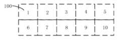
예를 들어, 복수의 발광 유닛(100)은 제 1 방향 및 제 2 방향을 따라 N행M열의 N*M어레이로 배열되며, N은 0보다 큰 정수이고, M은 0보다 큰 정수이다. 예를 들어, 제 1 방향과 제 2 방향은 교차된다. 예를 들어, 일부 예에서, 각 행의 발광 유닛(100)은 제 1 방향으로 배열되고, 각 열의 발광 유닛(100)은 제 2 방향으로 배열되고, 제 1 방향은 제 2 방향에 수직되고, 제 1 방향은 행방향이고, 제 2 방향은 열 방향이다. 물론, 본 발명의 실시예는 이에 제한되지 않고, 제 1 방향과 제 2 방향은 제 1 방향과 제 2 방향이 교차되는 한 임의의 방향일 수 있다.For example, a plurality of light-emitting units (100) are arranged in an N*M array of N rows and M columns along a first direction and a second direction, where N is an integer greater than 0 and M is an integer greater than 0. For example, the first direction and the second direction intersect. For example, in some examples, the light-emitting units (100) of each row are arranged in the first direction, the light-emitting units (100) of each column are arranged in the second direction, the first direction is perpendicular to the second direction, the first direction is a row direction, and the second direction is a column direction. Of course, the embodiments of the present invention are not limited thereto, and the first direction and the second direction can be any direction as long as the first direction and the second direction intersect.
예를 들어, 복수의 발광 유닛(100)은 직선으로 배열되는 것에 제한되지 않고, 곡선, 링형 또는 임의의 방식으로 배열될 수 있으며, 이는 실제 요구 사항에 따라 결정될 수 있고, 본 발명의 실시예는 이에 의해 제한되지 않는다. 예를 들어, 발광 유닛(100)의 수는 발광 기판(10)의 크기 및 요구되는 휘도 등 실제 요구 사항에 따라 결정될 수 있다. 도 2에서는 발광 유닛(100)을 4열5행으로 도시하였으나, 발광 유닛(100)개의 수가 이에 제한되지 않음을 이해해야 한다. 예를 들어, 베이스 기판(101)은 플라스틱 기판, 실리콘 기판, 세라믹 기판, 유리 기판, 석영 기판 등일 수 있고, 베이스 기판(101)은 단층 또는 다층 회로를 포함하며, 본 발명의 실시예는 이에 제한되지 않는다.For example, the plurality of light-emitting units (100) are not limited to being arranged in a straight line, but may be arranged in a curved, ring-shaped, or arbitrary manner, which may be determined according to actual requirements, and the embodiments of the present invention are not limited thereby. For example, the number of light-emitting units (100) may be determined according to actual requirements, such as the size of the light-emitting substrate (10) and the required brightness. In FIG. 2, the light-emitting units (100) are illustrated as four columns and five rows, but it should be understood that the number of light-emitting units (100) is not limited thereto. For example, the base substrate (101) may be a plastic substrate, a silicon substrate, a ceramic substrate, a glass substrate, a quartz substrate, or the like, and the base substrate (101) includes a single-layer or multi-layer circuit, and the embodiments of the present invention are not limited thereto.
도 4는 도 2에 도시된 발광 기판의 하나의 발광 유닛의 개략도이다. 예를 들어, 도 4에 도시된 바와 같이, 복수의 발광 유닛(100)의 경우, 각 발광 유닛(100)은 구동 회로(110), 복수의 발광 소자(120), 제 1 전압단(31) 및 제 2 전압단(32)을 포함한다.FIG. 4 is a schematic diagram of one light emitting unit of the light emitting substrate illustrated in FIG. 2. For example, as illustrated in FIG. 4, in the case of a plurality of light emitting units (100), each light emitting unit (100) includes a driving circuit (110), a plurality of light emitting elements (120), a first voltage terminal (31), and a second voltage terminal (32).
구동 회로(110)는 제 1 입력단(Di), 제 2 입력단(Pwr), 출력단(OT) 및 공통 전압단(GND)을 포함한다. 제 1 입력단(Di)은 대응하는 어드레스의 구동 회로(110)를 게이팅하기 위한 어드레스 신호와 같은 제 1 입력 신호를 수신한다. 예를 들어, 상이한 구동 회로(110)의 어드레스는 동일하거나 상이할 수 있다. 제 1 입력 신호는 8bit의 어드레스 신호일 수 있고, 전송할 어드레스는 당해 어드레스 신호를 파싱하여 획득할 수 있다. 제 2 입력단(Pwr)은 제 2 입력 신호를 수신하고, 제 2 입력 신호는 예를 들어 전력선 캐리어 통신 신호이다. 예를 들어, 제 2 입력 신호는 구동 회로(110)에 전원을 공급할 뿐만 아니라, 통신 데이터를 구동 회로(110)로 전송하고, 당해 통신 데이터를 이용하여 대응하는 발광 유닛(100)의 발광 기간을 제어하여, 시각적 발광 휘도를 제어할 수 있다. 출력단(OT)은 상이한 기간 내에 상이한 신호를 출력할 수 있으며, 예를 들어 각각 중계 신호 및 구동 신호를 출력할 수 있다. 예를 들어, 중계 신호는 다른 구동 회로(110)에 제공되는 어드레스 신호로서, 즉, 다른 구동 회로들(110)의 제 1 입력단(Di)이 당해 중계 신호를 제 1 입력 신호로서 수신하여, 어드레스 신호를 획득한다. 예를 들어, 구동 신호는 발광 소자(120)가 발광하도록 구동하기 위한 구동 전류일 수 있다. 공통 전압단(GND)은 접지 신호와 같은 공통 전압 신호를 수신한다. 예를 들어, 공통 전압단(GND)은 제 2 전압단(32)과 전기적으로 연결된다.The driving circuit (110) includes a first input terminal (Di), a second input terminal (Pwr), an output terminal (OT), and a common voltage terminal (GND). The first input terminal (Di) receives a first input signal, such as an address signal for gating the driving circuit (110) of a corresponding address. For example, addresses of different driving circuits (110) may be the same or different. The first input signal may be an 8-bit address signal, and an address to be transmitted may be obtained by parsing the address signal. The second input terminal (Pwr) receives a second input signal, and the second input signal is, for example, a power line carrier communication signal. For example, the second input signal may not only supply power to the driving circuit (110), but also transmit communication data to the driving circuit (110), and control a light emission period of a corresponding light emission unit (100) using the communication data, thereby controlling visual light emission brightness. The output terminal (OT) can output different signals within different periods, for example, can output a relay signal and a driving signal, respectively. For example, the relay signal is an address signal provided to another driving circuit (110), that is, the first input terminal (Di) of the other driving circuits (110) receives the relay signal as a first input signal and obtains the address signal. For example, the driving signal can be a driving current for driving the light-emitting element (120) to emit light. The common voltage terminal (GND) receives a common voltage signal such as a ground signal. For example, the common voltage terminal (GND) is electrically connected to the second voltage terminal (32).
구동 회로(110)는 제 1 입력단(Di)에 의해 수신된 제 1 입력 신호 및 제 2 입력단(Pwr)에 의해 수신된 제 2 입력 신호에 따라 제 1 기간 내에 출력단(OT)을 통해 중계 신호를 출력하고, 제 2 기간 내에 출력단(OT)을 통해 구동 신호를 순차적으로 직렬 연결된 복수의 발광 소자(120)에 제공한다. 제 1 기간 동안 출력단(OT)은 중계 신호를 출력하고, 당해 중계 신호는 다른 구동 회로(110)가 어드레스 신호를 획득하도록 다른 구동 회로(110)에 제공된다. 제 2 기간 동안 출력단(OT)은 구동 신호를 출력하고, 당해 구동 신호는 순차적으로 직렬 연결된 복수의 발광 소자(120)에 제공되어 제 2 기간 동안 발광 소자(120)가 발광된다.The driving circuit (110) outputs a relay signal through the output terminal (OT) within a first period according to a first input signal received by the first input terminal (Di) and a second input signal received by the second input terminal (Pwr), and provides the driving signal to a plurality of light-emitting elements (120) that are connected in series sequentially through the output terminal (OT) within a second period. During the first period, the output terminal (OT) outputs a relay signal, and the relay signal is provided to another driving circuit (110) so that the other driving circuit (110) obtains an address signal. During the second period, the output terminal (OT) outputs a driving signal, and the driving signal is provided to a plurality of light-emitting elements (120) that are connected in series sequentially, so that the light-emitting elements (120) emit light during the second period.
예를 들어, 제 1 기간과 제 2 기간은 상이한 기간이고, 예를 들어, 제 1 기간은 제 2 기간보다 빠를 수 있다. 제 1 기간은 제 2 기간과 연속적으로 인접될 수 있으며, 제 1 기간의 종료 시점은 제 2 기간의 시작 시점이고, 또는 제 1 기간과 제 2 기간 사이에 다른 기간이 있을 수도 있으며, 당해 다른 기간은 다른 필수 기능을 구현하는데 사용될 수 있으며, 당해 다른 기간은 제 1 기간과 제 2 기간을 분리하는데만 사용될 수도 있어, 제 1 구간과 제 2 구간에서 출력단(OT)의 신호가 서로 간섭하는 것을 방지한다.For example, the first period and the second period may be different periods, for example, the first period may be earlier than the second period. The first period may be continuously adjacent to the second period, and the end point of the first period is the start point of the second period, or there may be another period between the first period and the second period, and the other period may be used to implement another essential function, or the other period may be used only to separate the first period and the second period, thereby preventing the signals of the output terminal (OT) in the first period and the second period from interfering with each other.
예를 들어, 복수의 발광 소자(120)가 순차적으로 직렬 연결되고, 제 1 전압단(31)과 출력단(OT) 사이에 연결된다. 예를 들어, 복수의 발광 소자(120)는 복수의 마이크로 발광 다이오드(Micro-LED) 또는 복수의 미니 발광 다이오드(Mini-LED)를 포함할 수 있으며, 즉, 어느 하나의 발광 소자(120)는 Micro-LED 또는 Mini-LED일 수 있다. 예를 들어, 각 발광 소자(120)는 양극(+) 및 음극(-)(또는 애노드 및 캐소드라고도 지칭함)을 포함하고, 복수의 발광 소자(120)의 양극 및 음극은 순차적으로 직렬 연결되어, 제 1 전압단(31)과 출력단(OT) 사이에 전류 경로가 형성된다. 제 1 전압단(31)은 구동 전압 신호, 예를 들어 발광 소자(120)를 발광시켜야 하는 기간(제 2 기간)에는 고전압, 그 외 기간에는 저전압을 제공한다. 따라서, 제 2 기간에 구동 전압 신호(예를 들어, 구동 전류)는 제 1 전압단(31)으로부터 복수의 발광 소자(120)를 순차적으로 흐른 후, 구동 회로(110)의 출력단(OT)으로 흐른다. 복수의 발광 소자(120)는 구동전류가 흐를 때 발광하며, 구동 전류의 지속 시간을 조절하여, 발광 소자(120)의 발광 기간을 제어함으로써, 시각적인 발광 휘도를 제어할 수 있다.For example, a plurality of light-emitting elements (120) are sequentially connected in series and connected between a first voltage terminal (31) and an output terminal (OT). For example, the plurality of light-emitting elements (120) may include a plurality of micro light-emitting diodes (Micro-LEDs) or a plurality of mini light-emitting diodes (Mini-LEDs), that is, one of the light-emitting elements (120) may be a Micro-LED or a Mini-LED. For example, each light-emitting element (120) includes an anode (+) and a cathode (-) (also referred to as an anode and a cathode), and the anodes and cathodes of the plurality of light-emitting elements (120) are sequentially connected in series, so that a current path is formed between the first voltage terminal (31) and the output terminal (OT). The first voltage terminal (31) provides a driving voltage signal, for example, a high voltage during a period (a second period) in which the light-emitting element (120) is to emit light, and a low voltage during other periods. Therefore, in the second period, the driving voltage signal (e.g., driving current) flows sequentially from the first voltage terminal (31) to the plurality of light-emitting elements (120) and then to the output terminal (OT) of the driving circuit (110). The plurality of light-emitting elements (120) emit light when the driving current flows, and by controlling the duration of the driving current to control the light-emitting period of the light-emitting elements (120), the visual light-emitting brightness can be controlled.
예를 들어, 도 4에 도시된 바와 같이, 일 실시예에 있어서, 하나의 발광 유닛(100)이 6개의 발광 소자(120)를 포함하고, 당해 6개의 발광 소자(120)가 2행3열로 배열된다. 예를 들어, 당해 6개의 발광 소자(120)는 왼쪽에서 오른쪽으로, 위에서 아래로 (1, 1), (1, 2), (1, 3), (2, 1), (2, 2), (2, 3)으로 순차적으로 번호가 매겨지고. 매겨진 번호는 도 4에 도시된 바와 같다. 예를 들어, 6개의 발광 소자(120)가 직렬 연결된 경우, (2, 1) 위치의 발광 소자(120)를 직렬 연결의 시점으로 사용하고, (1, 1), (2, 2), (1, 2), (2, 3) 및 (1, 3) 위치의 발광 소자(120)가 차례로 연결되고, (1, 3) 위치의 발광 소자(120)를 직렬 연결의 종점으로 사용한다. 예를 들어, (2,1) 위치의 발광 소자(120)의 양극은 제 1 전압단(31)에 연결되고, (1,3) 위치의 발광 소자(120)의 음극은 구동 회로(110)의 출력단(OT)에 연결된다. 이러한 분배 방식과 직렬 연결 방식을 채택함으로써, 배선의 겹침을 효과적으로 방지할 수 있어, 설계 및 제조에 편리하며, 직렬 연결 상의 임의의 인접한 두 개의 발광 소자(120) 사이의 배선의 절곡 형상 및 길이가 거의 동일하여, 회로 자체의 저항이 비교적 균형되므로, 부하의 균형성을 향상시키고, 회로의 안정성을 향상시킬 수 있다.For example, as illustrated in FIG. 4, in one embodiment, one light emitting unit (100) includes six light emitting elements (120), and the six light emitting elements (120) are arranged in two rows and three columns. For example, the six light emitting elements (120) are sequentially numbered from left to right and top to bottom as (1, 1), (1, 2), (1, 3), (2, 1), (2, 2), (2, 3). The numbering is as illustrated in FIG. 4. For example, when six light-emitting elements (120) are connected in series, the light-emitting element (120) at the (2, 1) position is used as the starting point of the series connection, and the light-emitting elements (120) at the positions (1, 1), (2, 2), (1, 2), (2, 3), and (1, 3) are connected in sequence, and the light-emitting element (120) at the (1, 3) position is used as the end point of the series connection. For example, the anode of the light-emitting element (120) at the (2, 1) position is connected to the first voltage terminal (31), and the cathode of the light-emitting element (120) at the (1, 3) position is connected to the output terminal (OT) of the driving circuit (110). By adopting this distribution method and serial connection method, overlapping of wiring can be effectively prevented, which is convenient for design and manufacturing, and since the bending shape and length of the wiring between any two adjacent light-emitting elements (120) in the serial connection are almost the same, the resistance of the circuit itself is relatively balanced, so that the load balance can be improved and the stability of the circuit can be improved.
예를 들어, 동일한 발광 유닛(100)에서, 복수(예를 들어, 6개)의 발광 소자(120)가 어레이로 배열되어, 발광이 보다 균일할 수 있다. 구동 회로(110)는 복수의 발광 소자(120)에 의해 구성되는 어레이의 간극에 위치한다.For example, in the same light emitting unit (100), a plurality (for example, six) of light emitting elements (120) are arranged in an array so that light emission can be more uniform. The driving circuit (110) is located in the gap of the array formed by the plurality of light emitting elements (120).
본 발명의 실시예에서 각 발광 유닛(100)의 발광 소자(120)의 수는 제한되지 않고, 4개, 5개, 7개, 8개 등의 임의의 수일 수 있으며, 6개로 제한되지 않는다. 복수의 발광 소자(120)는 임의의 배열 방식이 채택될 수 있으며, 예를 들어 필요한 패턴으로 배열될 수 있으며, 매트릭스 배열에 제한되지 않는다. 구동 회로(110)의 설치 위치는 제한되지 않으며, 발광 소자(120) 사이의 임의의 간격에 설치될 수 있으며, 이는 실제 필요에 따라 결정될 수 있으며, 본 발명의 실시예는 이에 제한되지 않는다.In the embodiment of the present invention, the number of light-emitting elements (120) of each light-emitting unit (100) is not limited, and may be any number such as 4, 5, 7, 8, etc., and is not limited to 6. The plurality of light-emitting elements (120) may adopt any arrangement method, and may be arranged in a required pattern, for example, and is not limited to a matrix arrangement. The installation position of the driving circuit (110) is not limited, and may be installed at any interval between the light-emitting elements (120), which may be determined according to actual needs, and the embodiment of the present invention is not limited thereto.
제 1 전압단(31)은 구동 전압 신호를 수신하고 당해 구동 전압 신호를 발광 소자(120)에 제공할 수 있고, 공통 전압 신호를 수신하고 당해 공통 전압 신호를 발광 소자(120)에 제공할 수도 있다는 점에 유의해야 하고, 이는 구동 회로(110)의 실제 작동 방식과 복수의 발광 소자(120)의 직렬 연결 방식에 의해 결정될 수 있으며, 본 발명의 실시예는 이에 제한되지 않는다. 예를 들어, 구동 전압 신호의 레벨은 접지 신호와 같은 공통 전압 신호의 레벨보다 크다.It should be noted that the first voltage terminal (31) can receive a driving voltage signal and provide the driving voltage signal to the light emitting element (120), and can also receive a common voltage signal and provide the common voltage signal to the light emitting element (120), which can be determined by the actual operating method of the driving circuit (110) and the serial connection method of the plurality of light emitting elements (120), and the embodiment of the present invention is not limited thereto. For example, the level of the driving voltage signal is greater than the level of the common voltage signal, such as the ground signal.
도 4에 도시된 발광 유닛(100)의 구조는 예시에 불과하며, 본 발명의 실시예를 제한하는 것으로 이해되어서는 안 된다. 예를 들어, 다른 실시예에서, 발광 유닛(100)은 구동 회로(110)를 설정할 필요 없이 발광 소자(120)만을 포함할 수 있다. 이 경우, 패시브 매트릭스(Passive Matrix, PM) 구동 방식에 의해 각 발광 소자(120)를 구동할 수 있다. 예를 들어, 다른 실시예에서, 박막 트랜지스터(Thin Film Transistor, TFT)를 포함하는 회로가 발광 유닛(100)에 설치될 수도 있고, 액티브 매트릭스(Active Matrix, AM) 구동 방식이 사용되어, 당해 회로에 의해 발광 소자(120)가 액티브 구동될 수 있으며, 당해 회로는 예를 들어 일반적인 픽셀 회로이며, 커패시터 등의 디바이스를 포함할 수 있으며, 이 경우, 전술한 구동 회로(110)는 생략될 수 있다. 발광 유닛(100)은 또한 본 발명의 실시예들에 의해 제한되지 않는 임의의 다른 적절한 구조를 채택할 수 있다.The structure of the light emitting unit (100) illustrated in FIG. 4 is merely an example and should not be construed as limiting the embodiments of the present invention. For example, in another embodiment, the light emitting unit (100) may include only the light emitting elements (120) without the need to set the driving circuit (110). In this case, each light emitting element (120) may be driven by a passive matrix (PM) driving method. For example, in another embodiment, a circuit including a thin film transistor (TFT) may be installed in the light emitting unit (100), and an active matrix (AM) driving method may be used, so that the light emitting elements (120) may be actively driven by the circuit. The circuit may be, for example, a general pixel circuit and may include a device such as a capacitor, in which case the above-described driving circuit (110) may be omitted. The light emitting unit (100) may also adopt any other appropriate structure that is not limited by the embodiments of the present invention.
도 5a는 도 2에 도시된 발광 기판의 제 1 전압선 및 제 2 전압선을 확대한 개략도이고, 도 5b는 도 2에 도시된 발광 기판에서 마지막 행의 발광 유닛과 및 제 1 전압선 및 제 2 전압선의 연결 관계의 개략도이다.FIG. 5a is an enlarged schematic diagram of the first voltage line and the second voltage line of the light-emitting substrate illustrated in FIG. 2, and FIG. 5b is a schematic diagram of the connection relationship between the light-emitting unit of the last row and the first voltage line and the second voltage line of the light-emitting substrate illustrated in FIG. 2.
예를 들어, 도 2, 도 5a 및 도 5b에 도시된 바와 같이, 복수의 제 1 전압선(21)은 복수 열의 발광 유닛(100)과 일대일로 대응되고, 제 1 전압 신호를 전송하도록 구성된다. 예를 들어, 당해 제 1 전압 신호는 구동 전압 신호 또는 공통 전압 신호이다. 제 1 전압선(21)은 순차적으로 연결된 제 1 부분(211), 제 1 연결부(213) 및 제 2 부분(212)을 포함한다. 예를 들어, 동일한 제 1 전압선(21)에 대해, 제 1 부분(211)의 제 1 방향에 따른 폭은 제 2 부분(212)의 제 1 방향에 따른 폭보다 크다. 예를 들어, 동일한 제 1 전압선(21)에 대해, 상이한 위치에서 제 1 부분(211)의 제 1 방향에 따른 폭은 동일할 수 있고, 상이한 위치에서 제 2 부분(212)의 제 1 방향에 따른 폭은 상이할 수 있다. 예를 들어, 제 2 부분(212)의 제 1 방향에 따른 폭은 예를 들어, 제 1 연결부(213)와 연결되는 일단으로부터 후술할 바인딩 핀(41)과 연결되는 일단을 향하여 점차적으로 작아지고, 즉, 제 2 부분(212)은 배선 설계 요건을 충족시키기 위해 점차적으로 좁아진다.For example, as illustrated in FIG. 2, FIG. 5A and FIG. 5B, a plurality of first voltage lines (21) correspond one-to-one with a plurality of rows of light-emitting units (100) and are configured to transmit a first voltage signal. For example, the first voltage signal is a driving voltage signal or a common voltage signal. The first voltage line (21) includes a first portion (211), a first connection portion (213) and a second portion (212) that are sequentially connected. For example, for the same first voltage line (21), the width of the first portion (211) along the first direction is larger than the width of the second portion (212) along the first direction. For example, for the same first voltage line (21), the width of the first portion (211) in the first direction at different locations may be the same, and the width of the second portion (212) in the first direction at different locations may be different. For example, the width of the second portion (212) in the first direction gradually decreases from, for example, an end connected to the first connecting portion (213) toward an end connected to a binding pin (41) to be described later, i.e., the second portion (212) gradually narrows to satisfy a wiring design requirement.
예를 들어, 제 1 부분(211)은 제 2 방향을 따라 연장되며, 예를 들어, 비아홀을 통해 대응하는 열의 제 1 행의 발광 유닛(100) 내지 Y 행의 발광 유닛(100)의 제 1 전압단(31)에 전기적으로 연결된다. 도 2의 예에서, 제 1 부분(211)은 대응하는 열의 제 1 행의 발광 유닛(100) 내지 제3 행의 발광 유닛(100)의 제 1 전압단(31)에 전기적으로 연결된다.For example, the first portion (211) extends along the second direction and is electrically connected to the first voltage terminal (31) of the light emitting unit (100) of the first row to the light emitting unit (100) of the Y row of the corresponding column, for example, through a via hole. In the example of Fig. 2, the first portion (211) is electrically connected to the first voltage terminal (31) of the light emitting unit (100) of the first row to the light emitting unit (100) of the third row of the corresponding column.
도 2의 제 1 전압선(21)이 위치하는 막층은 발광 소자(120)의 베이스 기판(101)에 더 가까운 측에 위치하므로, 제 1 전압선(21)의 제 1 부분(211)은 발광 유닛(100)의 제 1 전압단(31)에 가까운 발광 소자(120)의 양극의 아래까지 연장되고 비아홀을 통해 당해 발광 소자(120)의 양극과 전기적으로 연결되고(즉, 제 1 전압단(31)과 전기적으로 연결됨), 즉, 제 1 전압선(21)은 제 1 전압 신호를 당해 발광 소자(120)의 양극으로 전송한다(즉, 제 1 전압단(31)으로 전송됨). 도 2에서는 발광 소자(120)의 음극이 제 1 전압선(21)과 중첩되지만, 양자가 상이한 막층에 위치하므로, 발광 소자(120)의 음극이 제 1 전압선(21)과 전기적으로 연결되지 않는다.Since the film layer where the first voltage line (21) of FIG. 2 is positioned is positioned closer to the base substrate (101) of the light-emitting element (120), the first portion (211) of the first voltage line (21) extends below the anode of the light-emitting element (120) close to the first voltage terminal (31) of the light-emitting unit (100) and is electrically connected to the anode of the light-emitting element (120) through the via hole (i.e., electrically connected to the first voltage terminal (31)), that is, the first voltage line (21) transmits the first voltage signal to the anode of the light-emitting element (120) (i.e., transmitted to the first voltage terminal (31)). In Fig. 2, the cathode of the light-emitting element (120) overlaps with the first voltage line (21), but since the two are located in different film layers, the cathode of the light-emitting element (120) is not electrically connected to the first voltage line (21).
복수의 제 1 전압선(21) 중 적어도 하나의 제 1 전압선(21)의 제 2 부분(212)의 연장 방향은 제 1 방향 및 제 2 방향과 모두 협각을 갖는다. 예를 들어, 당해 협각은 0도보다 크고 90도보다 작을(예를 들어, 20-70도, 40-60도, 또는 45도) 수 있고, 당해 연장 방향과 제 1 방향의 협각과 당해 연장 방향과 제 2 방향의 협각은 동일하거나 상이할 수 있다. 예를 들어, 도 2의 예에서, 적어도 하나의 제 1 전압선(21)의 제 2 부분(212)은 경사지게 연장되고, 즉, 행 방향 및 열 방향 모두에 대해 협각을 갖는다. 일부 제 1 전압선(21)의 제 2 부분(212)이 경사지게 연장되거나 전부 제 1 전압선(21)의 제 2 부분(212)이 경사지게 연장될 수 있으며, 이는 실제 배선 요구 사항에 따라 결정될 수 있고, 본 발명의 실시예는 이에 제한되지 않는다.The extension direction of the second portion (212) of at least one first voltage line (21) among the plurality of first voltage lines (21) has an included angle with both the first direction and the second direction. For example, the included angle may be greater than 0 degrees and less than 90 degrees (e.g., 20-70 degrees, 40-60 degrees, or 45 degrees), and the included angle between the extension direction and the first direction and the included angle between the extension direction and the second direction may be the same or different. For example, in the example of FIG. 2, the second portion (212) of at least one first voltage line (21) extends obliquely, that is, has an included angle with both the row direction and the column direction. Some of the second portions (212) of the first voltage lines (21) may be extended obliquely, or all of the second portions (212) of the first voltage lines (21) may be extended obliquely, which may be determined according to actual wiring requirements, and the embodiments of the present invention are not limited thereto.
제 1 연결부(213)는 제 Y 행의 발광 유닛(100)과 제 Y+1 행의 발광 유닛(100)의 경계부에 위치하며, 제 1 부분(211)과 제 2 부분(212)이 전기적으로 연결되도록 구성되고, 0<Y<N이고 Y는 정수이다. 예를 들어, 도 2의 예에서, 제 1 연결부(213)는 제 3 행의 발광 유닛(100)과 제 4 행의 발광 유닛(100)의 경계부에 위치하고, Y=3, N =4, Y=N-1이다. 예를 들어, 제 1 연결부(213)는 실제로 제 1 전압선(21)의 절곡된 부분이므로, 제 1 전압선(21)의 연장 방향이 변경된다. 제 1 연결부(213)가 포함하는 영역은 제한되지 않으며, 제 1 연결부(213)는 제 1 전압선(21)의 절곡 부분뿐만 아니라, 제 1 전압선(21)의 제 2 방향을 따라 연장되는 세그먼트의 일부를 포함할 수도 있으며, 제 1 전압선(21)의 경사지게 연장되는 세그먼트의 일부를 포함할 수도 있으며, 본 발명의 실시예는 이에 제한되지 않는다.The first connecting portion (213) is located at the boundary between the light emitting unit (100) of the Yth row and the light emitting unit (100) of the Y+1th row, and is configured such that the first part (211) and the second part (212) are electrically connected, where 0<Y<N and Y is an integer. For example, in the example of FIG. 2, the first connecting portion (213) is located at the boundary between the light emitting unit (100) of the third row and the light emitting unit (100) of the fourth row, and Y=3, N=4, Y=N-1. For example, since the first connecting portion (213) is actually a bent portion of the first voltage line (21), the extension direction of the first voltage line (21) is changed. The area included in the first connecting portion (213) is not limited, and the first connecting portion (213) may include not only the bent portion of the first voltage line (21), but also a portion of a segment extending along the second direction of the first voltage line (21), and may also include a portion of a segment extending obliquely of the first voltage line (21), and the embodiment of the present invention is not limited thereto.
복수의 제 1 전송선(22)은 복수의 발광 유닛(100)과 일대일로 대응된다. 제 1 전송선(22)은 대응하는 열의 제 Y+1 행의 발광 유닛(100) 내지 제 N 행의 발광 유닛(100)의 제 1 전압단(31)과 전기적으로 연결되고, 대응하는 열의 발광 유닛(100)의 대응하는 제 1 전압선의 제 1 연결부에 전기적으로 연결된다. 예를 들어, 도 2의 예에서, 제 1 전송선(22)은 대응하는 열의 제 4 행의 발광 유닛(100)의 제 1 전압단(31)과 전기적으로 연결되고, 대응하는 열의 발광 유닛(100)의 대응하는 제 1 전압선(21)의 제 1 연결부(213)가 전기적으로 연결되어, 제 4 행의 발광 유닛(100)의 제 1 전압단(31)과 제 1 전압선이 전기적으로 연결되므로, 제 1 전압선(21)에 의해 제공되는 제 1 전압 신호가 수신될 수 있다. 이때, Y=3, N=4, Y=N-1이다.A plurality of first transmission lines (22) correspond one-to-one with a plurality of light-emitting units (100). The first transmission line (22) is electrically connected to the first voltage terminal (31) of the light-emitting unit (100) of the Y+1-th row to the N-th row of the corresponding column, and is electrically connected to the first connection part of the corresponding first voltage line of the light-emitting unit (100) of the corresponding column. For example, in the example of FIG. 2, the first transmission line (22) is electrically connected to the first voltage terminal (31) of the light-emitting unit (100) of the fourth row of the corresponding column, and the first connection portion (213) of the corresponding first voltage line (21) of the light-emitting unit (100) of the corresponding column is electrically connected, so that the first voltage terminal (31) of the light-emitting unit (100) of the fourth row and the first voltage line are electrically connected, so that the first voltage signal provided by the first voltage line (21) can be received. At this time, Y=3, N=4, Y=N-1.
예를 들어, 제 1 전압선(21)과 제 1 전송선(22)은 상이한 층에 위치하여, 배선이 용이할 수 있다. 예를 들어, 제 1 전압선(21)과 제 1 전송선(22) 사이의 전기적 연결은 비아홀을 통해 이루어질 수 있다. 물론, 본 발명의 실시예는 이에 제한되지 않고, 제 1 전압선(21)과 제 1 전송선(22)이 동일한 층에 위치할 수도 있음은 물론이고, 다른 구조와 단락 없이 대응하는 전기적 연결이 이루어질 수 있으면 된다. 예를 들어, 제 1 전압선(21)의 제 1 부분(211)의 제 1 방향에 따른 폭은 제 1 전송선(22)의 제 1 방향에 따른 폭보다 크다.For example, the first voltage line (21) and the first transmission line (22) may be located on different layers, so that wiring may be easy. For example, the electrical connection between the first voltage line (21) and the first transmission line (22) may be formed through a via hole. Of course, the embodiment of the present invention is not limited thereto, and the first voltage line (21) and the first transmission line (22) may be located on the same layer, and as long as a corresponding electrical connection can be formed without a short circuit with another structure, it is sufficient. For example, the width of the first portion (211) of the first voltage line (21) along the first direction is larger than the width of the first transmission line (22) along the first direction.
본 발명의 설명에서 "상이한 층"에 위치한다는 것은 상이한 막층에 위치하는 것을 의미하며, 이러한 상이한 막층은 비아홀이 제공되지 않은 위치에서 서로 절연됨을 유의해야 한다. 예를 들어, 상이한 막층에 위치된 배선(예를 들어 제 1 전압선(21)과 제 1 전송선(22))이 서로 전기적으로 연결해야 하는 경우, 비아홀을 설치하는 방식으로 상이한 막층에 위치한 배선의 전기적 연결을 구현할 수 있다. 예를 들어, 이러한 상이한 막층은 상이한 프로세스로 제조되고, 예를 들어 제 1 프로세스를 사용하여 이러한 상이한 막층 중 하나의 막층을 제조한 후, 제 2 프로세스를 사용하여 이러한 상이한 층 중 다른 막층을 제조한다. 예를 들어, 제 1 프로세스가 수행된 후 제 2 프로세스가 수행되기 전에, 제3 프로세스를 사용하여 절연층을 제조할 수도 있고, 당해 절연층은 상이한 막층 사이에 위치하여, 상이한 막층이 비아홀이 설치되지 않은 위치에서 서로 절연되도록 한다. 예를 들어, 제 1 프로세스, 제 2 프로세스 및 제3 프로세스는 동일하거나 상이할 수 있다. 예를 들어, 베이스 기판(101)에 수직인 방향에서, 상이한 막층으로부터 베이스 기판(101)까지의 거리가 상이하다. 즉, 상이한 막층 중 하나의 막층은 베이스 기판(101)에 가깝고, 다른 하나의 막층은 베이스 기판(101)에서 멀다. 이하의 설명에서, "상이한 층"에 위치한다는 의미는 상기 설명을 참조할 수 있으며, 중복되는 설명은 생략한다.In the description of the present invention, positioning in "different layers" means positioning in different film layers, and it should be noted that these different film layers are insulated from each other at positions where via holes are not provided. For example, when wirings (e.g., the first voltage line (21) and the first transmission line (22)) positioned in different film layers need to be electrically connected to each other, the electrical connection of the wirings positioned in the different film layers can be implemented by installing via holes. For example, these different film layers are manufactured by different processes, and for example, one film layer of these different film layers is manufactured using a first process, and then another film layer of these different layers is manufactured using a second process. For example, after the first process is performed and before the second process is performed, an insulating layer can be manufactured using a third process, and the insulating layer is located between the different film layers so that the different film layers are insulated from each other at positions where via holes are not installed. For example, the first process, the second process, and the third process can be the same or different. For example, in the direction perpendicular to the base substrate (101), the distances from different film layers to the base substrate (101) are different. That is, one film layer among the different film layers is close to the base substrate (101), and the other film layer is far from the base substrate (101). In the following description, the meaning of being located in a "different layer" may refer to the above description, and any duplicate description will be omitted.
본 발명의 설명에서 "동일한 층"에 위치한다는 것은 동일한 막층에 있는 것을 의미한다는 점에 유의해야 한다. 예를 들어, 동일한 막층에 위치한 배선은 동일한 프로세스에 의해 제조될 수 있고, 예를 들어 필요한 배선은 1회의 패터닝 프로세스에 의해 형성된다. 예를 들어, 베이스 기판(101)에 수직인 방향에서, 동일한 막층에 위치한 배선과 베이스 기판(101) 사이의 거리는 동일하거나 실질적으로 동일하다. 즉, 당해 막층의 배선과 베이스 기판(101) 사이의 거리는 동일하거나 실질적으로 동일하다. 이하의 설명에서 "동일한 층"에 위치한다는 의미는 상기 설명을 참조할 수 있으며, 중복되는 설명은 생략한다.It should be noted that in the description of the present invention, positioned in the "same layer" means positioned in the same film layer. For example, wiring positioned in the same film layer can be manufactured by the same process, and for example, required wiring is formed by a single patterning process. For example, in the direction perpendicular to the base substrate (101), the distance between the wiring positioned in the same film layer and the base substrate (101) is the same or substantially the same. That is, the distance between the wiring in the film layer and the base substrate (101) is the same or substantially the same. In the following description, the meaning of positioned in the "same layer" may refer to the above description, and redundant description will be omitted.
도 2에 도시된 예에서, 제 1 전압선(21)의 제 1 부분(211)이 제 2 방향(즉, 열 방향)을 따라 연장되어 있으므로, 동일한 열에 위치한 제 1 행의 발광 유닛(100) 내지 제 3 행의 발광 유닛(100)의 제 1 전압단(31)은 베이스 기판(101) 상의 제 1 전압선(21)의 정사영 내부에 위치한다(예를 들어, 베이스 기판(101) 상의 제 1 부분(211)의 정사영 내부에 위치됨). 따라서, 제 1 행의 발광 유닛(100) 내지 제 3 행의 발광 유닛(100)에 대하여, 제 1 전압단(31)의 위치에 비아홀을 설치하여 제 1 전압단(31)과 제 1 전압선(21)의 전기적 연결을 구현할 수 있다. 제 1 전압선(21)의 제 2 부분(212)은 경사지게 연장되고, 제 4 행의 발광 유닛(100)의 제 1 전압단(31)은 베이스 기판(101) 상의 제 1 전압선(21)의 정사영 외부에 위치하고(예를 들어 베이스 기판(101) 상의 제 2 부분(212)의 정사영 외부에 위치됨), 따라서 제 4 행의 발광 유닛(100)에 대해, 제 1 전압단(31)의 위치에 비아홀 설치하는 것에 의해 제 1 전압단(31)과 제 1 전압선(21)의 전기적 연결을 구현할 수 없고, 제 1 전송선(22)을 설치하는 것에 의해 제 1 전압단(31)과 제 1 전압선(21)을 전기적으로 연결해야 한다.In the example illustrated in FIG. 2, since the first portion (211) of the first voltage line (21) extends along the second direction (i.e., the column direction), the first voltage terminals (31) of the light-emitting units (100) of the first row to the third row located in the same column are located within the orthogonal projection of the first voltage line (21) on the base substrate (101) (for example, located within the orthogonal projection of the first portion (211) on the base substrate (101). Accordingly, for the light-emitting units (100) of the first row to the third row, a via hole can be installed at the position of the first voltage terminal (31) to implement an electrical connection between the first voltage terminal (31) and the first voltage line (21). The second portion (212) of the first voltage line (21) is extended obliquely, and the first voltage terminal (31) of the light-emitting unit (100) of the fourth row is located outside the orthogonal projection of the first voltage line (21) on the base substrate (101) (for example, located outside the orthogonal projection of the second portion (212) on the base substrate (101)). Therefore, for the light-emitting unit (100) of the fourth row, the electrical connection between the first voltage terminal (31) and the first voltage line (21) cannot be realized by installing a via hole at the position of the first voltage terminal (31), and the first voltage terminal (31) and the first voltage line (21) must be electrically connected by installing a first transmission line (22).
제 1 전압선(21)을 발광 기판(10)의 가장자리(예를 들어, 도 2에 도시된 발광 기판(10)의 하부 가장자리)로부터 먼 위치로부터 시작하여 경사지게 연장하고 점차적으로 좁아지게 함으로써, 각 행의 발광 유닛(100) 중의 제 1 전압단(31)과 제 1 전압선(21) 사이의 전기적 연결을 보장하였고, 경사진 배선 영역을 효과적으로 감소시키고, 발광 기판(10)의 베젤을 감소시킬 수 있어, 비표시 영역의 폭(L2)이 작아지고, 발광 기판(10)의 비표시 영역의 크기를 감소시키는데 유리하고, 내로 베젤 설계를 구현하는데 유리하다.By starting from a position far from the edge of the light-emitting substrate (10) (for example, the lower edge of the light-emitting substrate (10) as shown in FIG. 2), extending obliquely and gradually narrowing the first voltage line (21) to ensure electrical connection between the first voltage terminal (31) of the light-emitting unit (100) of each row and the first voltage line (21), the inclined wiring area can be effectively reduced, and the bezel of the light-emitting substrate (10) can be reduced, so that the width (L2) of the non-display area becomes smaller, which is advantageous in reducing the size of the non-display area of the light-emitting substrate (10), and is advantageous in implementing a narrow bezel design.
당해 예에서, 제 1 전송선(22)은 제 2 방향을 따라 제 1 연결부(213)까지 연장되고, 비아홀을 통해 제 1 연결부(213)에 전기적으로 연결되어, 제 1 전송선(22)의 배선이 용이하고, 배선 설계를 간략화하는데 유리하다. 그러나, 본 발명의 실시예는 이에 제한되지 않고, 제 1 전송선(22)도 임의의 방향을 따라 연장되고 제 1 전압선(21)의 임의의 부분(예를 들어 제 1 부분(211) 또는 제 2 부분(212))과 전기적으로 연결될 수 있고, 이는 실제 요구 사항에 따라 결정될 수 있으며, 예를 들어 실제 배선 설계에 따라 결정될 수 있으며, 본 발명의 실시예는 이에 제한되지 않는다.In the present example, the first transmission line (22) extends along the second direction to the first connection portion (213) and is electrically connected to the first connection portion (213) through a via hole, so that the wiring of the first transmission line (22) is easy and the wiring design is simplified. However, the embodiment of the present invention is not limited thereto, and the first transmission line (22) may also extend along an arbitrary direction and be electrically connected to an arbitrary portion (for example, the first portion (211) or the second portion (212)) of the first voltage line (21), which may be determined according to actual requirements, for example, may be determined according to an actual wiring design, and the embodiment of the present invention is not limited thereto.
예를 들어, 도 2, 도 5a 및 도 5b에 도시된 바와 같이, 당해 발광 기판(10)은 복수의 제 2 전압선(23) 및 복수의 제 2 전송선(24)을 더 포함한다. 복수의 제 2 전압선(23)은 다열의 발광 유닛(100)에 일대일로 대응하며, 제 2 전압 신호를 전송하도록 구성된다. 예를 들어, 당해 제 2 전압 신호는 공통 전압 신호 또는 구동 전압 신호이다. 전술한 제 1 전압 신호가 구동 전압 신호인 경우, 당해 제 2 전압 신호는 공통 전압 신호이고, 제 1 전압 신호의 레벨이 제 2 전압 신호의 레벨보다 크고, 전술한 제 1 전압 신호가 공통 전압 신호인 경우, 당해 제 2 전압 신호는 구동 전압 신호이고, 제 1 전압 신호의 레벨은 제 2 전압 신호의 레벨보다 작다. 예를 들어, 공통 전압 신호는 접지 신호이다. 제 1 전압 신호 및 제 2 전압 신호의 구체적인 레벨 및 신호 유형은 실제 요구 사항, 예를 들어 발광 유닛(100)의 구조적 형태 및 작동 방식에 따라 결정될 수 있으며, 본 발명의 실시예는 이에 제한되지 않는다.For example, as illustrated in FIG. 2, FIG. 5A and FIG. 5B, the light-emitting substrate (10) further includes a plurality of second voltage lines (23) and a plurality of second transmission lines (24). The plurality of second voltage lines (23) correspond one-to-one to the light-emitting units (100) in multiple rows and are configured to transmit a second voltage signal. For example, the second voltage signal is a common voltage signal or a driving voltage signal. When the above-described first voltage signal is a driving voltage signal, the second voltage signal is a common voltage signal, and the level of the first voltage signal is greater than the level of the second voltage signal, and when the above-described first voltage signal is a common voltage signal, the second voltage signal is a driving voltage signal, and the level of the first voltage signal is less than the level of the second voltage signal. For example, the common voltage signal is a ground signal. The specific levels and signal types of the first voltage signal and the second voltage signal may be determined according to actual requirements, for example, the structural form and operating method of the light emitting unit (100), and the embodiments of the present invention are not limited thereto.
예를 들어, 제 2 전압선(23)은 순차적으로 연결된 제3 부분(231), 제 2 연결부(233) 및 제4 부분(232)을 포함한다. 예를 들어, 동일한 제 2 전압선(23)에 대해, 제3 부분(231)의 제 1 방향에 따른 폭은 제4 부분(232)의 제 1 방향에 따른 폭보다 크다. 예를 들어, 동일한 제 2 전압선(23)에 대해, 상이한 위치에서 제3 부분(231)의 제 1 방향에 따른 폭은 동일할 수 있고, 상이한 위치에서 제4 부분(232)의 제 1 방향에 따른 폭이 상이할 수 있다. 예를 들어, 제4 부분(232)의 제 1 방향에 따른 폭은 예를 들어, 제 2 연결부(233)와 연결되는 일단으로부터 후술할 바인딩 핀(41)과 연결되는 일단을 향해 점차적으로 감소되고, 즉, 제4 부분(232)은 배선 설계 요건을 충족시키기 위해 점차적으로 좁아진다.For example, the second voltage line (23) includes a third portion (231), a second connection portion (233), and a fourth portion (232) that are sequentially connected. For example, for the same second voltage line (23), the width of the third portion (231) along the first direction is larger than the width of the fourth portion (232) along the first direction. For example, for the same second voltage line (23), the widths of the third portions (231) along the first direction at different locations may be the same, and the widths of the fourth portions (232) along the first direction at different locations may be different. For example, the width of the fourth portion (232) along the first direction gradually decreases from, for example, an end connected to the second connection portion (233) toward an end connected to a binding pin (41) to be described later, i.e., the fourth portion (232) gradually narrows to satisfy the wiring design requirements.
예를 들어, 제3 부분(231)은 제 2 방향을 따라 연장되고, 비아홀 등을 통해 대응하는 열의 제 1 행의 발광 유닛(100) 내지 제 Y 행의 발광 유닛(100)의 제 2 전압단(32)에 전기적으로 연결된다. 도 2의 예에서, 제3 부분(231)은 대응하는 열의 제 1 행의 발광 유닛(100) 내지 제 3 행의 발광 유닛(100)의 제 2 전압단(32)에 전기적으로 연결된다.For example, the third portion (231) extends along the second direction and is electrically connected to the second voltage terminal (32) of the light emitting unit (100) of the first row to the light emitting unit (100) of the Y-th row of the corresponding column through a via hole or the like. In the example of Fig. 2, the third portion (231) is electrically connected to the second voltage terminal (32) of the light emitting unit (100) of the first row to the light emitting unit (100) of the third row of the corresponding column.
도 2의 제 2 전압선(23)이 위치하는 막층은 구동 회로(110)의 베이스 기판(101)에 가까운 측에 위치하므로, 제 2 전압선의 제3 부분(231)은 구동 회로(110)의 공통 전압단(GND) 아래까지 연장되고 비아홀을 통해 당해 구동 회로(110)의 공통 전압단(GND)과 전기적으로 연결되고(즉, 제 2 전압단(32)과 전기적으로 연결됨), 즉, 제 2 전압선(23)은 제 2 전압 신호를 당해 구동 회로(110)의 공통 전압단(GND)으로 전송한다(즉, 제 2 전압단(32)으로 전송한다). 도 2에서는 구동 회로(110)의 다른 포트 및 발광 소자(120)와 제 2 전압선(23)이 중첩되지만, 제 2 전압선(23)은 구동 회로(110) 및 발광소자(120)가 위치하는 막층과 상이한 막층에 위치하기 때문에, 구동 회로(110)의 다른 포트 및 발광 소자(120)와 제 2 전압선(23)이 전기적으로 연결되지 않는다.Since the film layer where the second voltage line (23) of FIG. 2 is located is located on the side closer to the base substrate (101) of the driving circuit (110), the third portion (231) of the second voltage line extends below the common voltage terminal (GND) of the driving circuit (110) and is electrically connected to the common voltage terminal (GND) of the driving circuit (110) through the via hole (i.e., electrically connected to the second voltage terminal (32)), that is, the second voltage line (23) transmits the second voltage signal to the common voltage terminal (GND) of the driving circuit (110) (i.e., transmits it to the second voltage terminal (32)). In FIG. 2, the other port of the driving circuit (110) and the light-emitting element (120) overlap with the second voltage line (23), but since the second voltage line (23) is located in a different film layer from the film layer where the driving circuit (110) and the light-emitting element (120) are located, the other port of the driving circuit (110) and the light-emitting element (120) and the second voltage line (23) are not electrically connected.
복수의 제 2 전압선(23) 중 적어도 하나의 제 2 전압선(23)의 제4 부분(232)이 연장되는 방향은 제 1 방향 및 제 2 방향 모두와 협각을 갖는다. 예를 들어, 협각은 0도보다 크고 90도보다 작을(예를 들어, 20-70도, 40-60도, 또는 45도) 수 있고, 당해 연장 방향과 제 1 방향 사이의 협각은 당해 연장 방향과 제 2 방향 사이의 협각과 동일하거나 상이할 수 있다. 예를 들어, 도 2의 예에서, 적어도 하나의 제 2 전압선(23)의 제4 부분(232)은 경사지게 연장되고, 즉 행 방향 및 열 방향 모두와 협각을 갖는다. 일부 제 2 전압선(23)의 제4 부분(232)이 경사지게 연장되거나, 전부 제 2 전압선(23)의 제4 부분(232)이 경사지게 연장될 수 있으며, 이는 실제 배선 요구 사항에 따라 결정될 수 있고, 본 발명의 실시예는 이에 제한되지 않는다.The direction in which the fourth portion (232) of at least one second voltage line (23) among the plurality of second voltage lines (23) extends has an included angle with both the first direction and the second direction. For example, the included angle may be greater than 0 degrees and less than 90 degrees (e.g., 20-70 degrees, 40-60 degrees, or 45 degrees), and the included angle between the extension direction and the first direction may be the same as or different from the included angle between the extension direction and the second direction. For example, in the example of FIG. 2, the fourth portion (232) of at least one second voltage line (23) extends obliquely, that is, has an included angle with both the row direction and the column direction. Some of the fourth portions (232) of the second voltage lines (23) may be extended obliquely, or all of the fourth portions (232) of the second voltage lines (23) may be extended obliquely, which may be determined according to actual wiring requirements, and the embodiments of the present invention are not limited thereto.
제 2 연결부(233)는 제 Y 행의 발광 유닛(100)과 제 Y+1 행의 발광 유닛(100)의 경계부에 위치하며, 제3 부분(231)과 제4 부분(232)이 전기적으로 연결하도록 구성되고, 0<Y<N이고 Y는 정수이다. 예를 들어, 도 2의 예에서, 제 2 연결부(233)는 제3 행의 발광 유닛(100)과 제4 행의 발광 유닛(100)의 경계부에 위치하고, 이때 Y=3, N=4, Y=N-1이다. 예를 들어, 제 2 연결부(233)는 실제로 제 2 전압선(23)의 절곡된 부분이므로, 제 2 전압선(23)의 연장 방향이 변경된다. 제 2 연결부(233)가 포함하는 영역은 제한되지 않고, 제 2 연결부(233)는 제 2 전압선(23)의 절곡 부분을 포함할 수 있을 뿐만 아니라, 제 2 전압선(23)의 제 2 방향을 따라 연장되는 세그먼트의 일부를 포함할 수도 있고, 제 2 전압선(23)의 경사지게 연장되는 세그먼트의 일부를 포함할 수도 있으며, 본 발명의 실시예는 이에 제한되지 않는다.The second connecting portion (233) is located at the boundary between the light emitting unit (100) of the Yth row and the light emitting unit (100) of the Y+1th row, and is configured to electrically connect the third portion (231) and the fourth portion (232), where 0<Y<N and Y is an integer. For example, in the example of FIG. 2, the second connecting portion (233) is located at the boundary between the light emitting unit (100) of the third row and the light emitting unit (100) of the fourth row, and at this time, Y=3, N=4, Y=N-1. For example, since the second connecting portion (233) is actually a bent portion of the second voltage line (23), the extension direction of the second voltage line (23) is changed. The area included in the second connecting portion (233) is not limited, and the second connecting portion (233) may not only include a bent portion of the second voltage line (23), but may also include a portion of a segment extending along the second direction of the second voltage line (23), and may also include a portion of a segment extending obliquely of the second voltage line (23), and the embodiment of the present invention is not limited thereto.
복수의 제 2 전송선(24)은 다열의 발광 유닛(100)과 일대일로 대응된다. 제 2 전송선(24)은 대응하는 열의 제 Y 행의 발광 유닛(100) 내지 제N 행의 발광 유닛(100)의 제 2 전압단(32)에 전기적으로 연결되고, 대응하는 열의 발광 유닛(100)에 대응하는 제 2 전압선(23)의 제 2 연결부(233)에 전기적으로 연결된다. 예를 들어, 도 2의 예에서, 제 2 전송선(24)은 대응하는 열의 제4 행의 발광 유닛(100)의 제 2 전압단(32)에 전기적으로 연결되고, 대응하는 열의 발광 유닛(100)에 대응하는 제 2 전압선(23)의 제 2 연결부(233)에 전기적으로 연결되기 때문에, 제4 행의 발광 유닛(100)의 제 2 전압단(32)이 제 2 전압선(23)에 전기적으로 연결되므로, 제 2 전압선(23)에 의해 제공되는 제 2 전압 신호가 수신될 수 있고, 이때, Y=3, N=4, Y=N-1이다.A plurality of second transmission lines (24) correspond one-to-one with the light-emitting units (100) of the multiple rows. The second transmission lines (24) are electrically connected to the second voltage terminals (32) of the light-emitting units (100) of the Y-th row to the N-th row of the corresponding columns, and are electrically connected to the second connection portion (233) of the second voltage line (23) corresponding to the light-emitting units (100) of the corresponding rows. For example, in the example of FIG. 2, the second transmission line (24) is electrically connected to the second voltage terminal (32) of the light-emitting unit (100) of the fourth row of the corresponding column, and is electrically connected to the second connection portion (233) of the second voltage line (23) corresponding to the light-emitting unit (100) of the corresponding column, so that the second voltage terminal (32) of the light-emitting unit (100) of the fourth row is electrically connected to the second voltage line (23), and thus the second voltage signal provided by the second voltage line (23) can be received, and at this time, Y=3, N=4, Y=N-1.
예를 들어, 제 2 전압선(23)과 제 2 전송선(24)은 상이한 층에 위치하여, 배선이 용이할 수 있다. 예를 들어, 제 2 전압선(23)과 제 2 전송선(24) 사이의 전기적 연결은 비아홀을 통해 이루어질 수 있다. 본 발명의 실시예가 이에 한정되는 것은 아니며, 제 2 전압선(23)과 제 2 전송선(24)이 동일한 층에 위치할 수도 있음은 물론이고, 다른 구조와 단락 없이 대응하는 전기적 연결이 이루어질 수 있으면 된다. 예를 들어, 제 2 전압선(23)의 제4 부분(232)의 제 1 방향에 따른 폭은 제 2 전송선(24)의 제 1 방향에 따른 폭보다 크다.For example, the second voltage line (23) and the second transmission line (24) may be located on different layers, so that wiring may be easy. For example, the electrical connection between the second voltage line (23) and the second transmission line (24) may be made through a via hole. The embodiment of the present invention is not limited thereto, and the second voltage line (23) and the second transmission line (24) may be located on the same layer, and as long as a corresponding electrical connection can be made without a short circuit with another structure, it is sufficient. For example, the width of the fourth portion (232) of the second voltage line (23) along the first direction is larger than the width of the second transmission line (24) along the first direction.
예를 들어, 제 1 전압선(21)과 제 2 전압선(23)은 동일한 층에 위치하고, 제 1 전송선(22)과 제 2 전송선(24)은 동일한 층에 위치하며, 제 1 전압선(21)과 제 1 전송선(22)은 상이한 층에 위치할 수 있다. 따라서, 제 1 전압선(21), 제 2 전압선(23), 제 1 전송선(22) 및 제 2 전송선(24)은 2개의 막층을 사용하여 설치될 수 있으며, 제 1 전압선(21) 및 제 2 전압선(23)은 그 중 하나의 막층에 위치하고, 제 1 전송선(22) 및 제 2 전송선(24)은 다른 막층에 위치하므로, 프로세스가 단순화되고, 단락이 방지될 수 있다.For example, the first voltage line (21) and the second voltage line (23) may be located in the same layer, the first transmission line (22) and the second transmission line (24) may be located in the same layer, and the first voltage line (21) and the first transmission line (22) may be located in different layers. Accordingly, the first voltage line (21), the second voltage line (23), the first transmission line (22) and the second transmission line (24) may be installed using two film layers, and the first voltage line (21) and the second voltage line (23) may be located in one of the film layers, and the first transmission line (22) and the second transmission line (24) may be located in another film layer, so that the process is simplified and short circuits can be prevented.
도 2에 도시된 예에서, 제 2 전압선(23)의 제3 부분(231)이 제 2 방향(즉, 열 방향)으로 연장되어 있으므로, 제 1 열의 제 1 행의 발광 유닛(100) 내지 제3 행의 발광 유닛(100)의 제 2 전압단(32)은 베이스 기판(101) 상의 제 2 전압선(23)의 정사영 내부에 위치하고(예를 들어, 베이스 기판(101) 상의 제3 부분(231)의 정사영 내부), 따라서, 제 1 행의 발광 유닛(100) 내지 제3 행의 발광 유닛(100)에 대해, 제 2 전압단(32)의 위치에 비아홀을 설치하여 제 2 전압단(32)과 제 2 전압선(23) 사이의 전기적 연결이 구현될 수 있다. 제 2 전압선(23)의 제4 부분(232)은 경사지게 연장되고, 제4 행의 발광 유닛(100)의 제 2 전압단(32)은 베이스 기판(101) 상의 제 2 전압선(23)의 정사영 외부에 위치하고(예를 들어 베이스 기판(101) 상의 제4 부분(232)의 정사영 외부), 따라서 제4 행의 발광 유닛(100)에 대해, 제 2 전압단(32)의 위치에 비아홀을 설치하는 것에 의해 제 2 전압단(32)과 제 2 전압선(23) 사이의 전기적 연결이 구현될 수 없고, 제 2 전송선(24)을 설치하여 제 2 전압단(32)과 제 2 전압선(23)을 전기적으로 연결해야 한다.In the example illustrated in FIG. 2, since the third portion (231) of the second voltage line (23) extends in the second direction (i.e., in the column direction), the second voltage terminal (32) of the light-emitting unit (100) of the first row of the first column to the light-emitting unit (100) of the third row is positioned within the orthogonal projection of the second voltage line (23) on the base substrate (101) (e.g., within the orthogonal projection of the third portion (231) on the base substrate (101)), and therefore, for the light-emitting unit (100) of the first row to the light-emitting unit (100) of the third row, an electrical connection between the second voltage terminal (32) and the second voltage line (23) can be implemented by installing a via hole at the position of the second voltage terminal (32). The fourth portion (232) of the second voltage line (23) is extended obliquely, and the second voltage terminal (32) of the light-emitting unit (100) of the fourth row is located outside the orthogonal projection of the second voltage line (23) on the base substrate (101) (for example, outside the orthogonal projection of the fourth portion (232) on the base substrate (101)). Therefore, for the light-emitting unit (100) of the fourth row, an electrical connection between the second voltage terminal (32) and the second voltage line (23) cannot be implemented by installing a via hole at the position of the second voltage terminal (32), and a second transmission line (24) must be installed to electrically connect the second voltage terminal (32) and the second voltage line (23).
제 2 전압선(23)을 발광 기판(10)의 가장자리(예를 들어, 도 2에 도시된 발광 기판(10)의 하부 가장자리)로부터 먼 위치로부터 시작하여 경사지게 연장하고 점차적으로 좁아지게 함으로써, 각 행의 발광 유닛(100) 중의 제 2 전압단(32)과 제 2 전압선(23) 사이의 전기적 연결을 보장하였고, 경사진 배선 영역을 효과적으로 감소시키고, 발광 기판(10)의 베젤을 감소시킬 수 있어, 비표시 영역의 폭(L2)이 작아지고, 발광 기판(10)의 비표시 영역의 크기를 감소시키는데 유리하고, 내로 베젤 설계를 구현하는데 유리하다.By starting the second voltage line (23) from a position far from the edge of the light-emitting substrate (10) (for example, the lower edge of the light-emitting substrate (10) as shown in FIG. 2) and extending obliquely and gradually narrowing, the electrical connection between the second voltage terminal (32) and the second voltage line (23) of the light-emitting units (100) of each row is ensured, the oblique wiring area is effectively reduced, and the bezel of the light-emitting substrate (10) can be reduced, so that the width (L2) of the non-display area becomes smaller, which is advantageous in reducing the size of the non-display area of the light-emitting substrate (10), and is advantageous in implementing a narrow bezel design.
당해 예에서, 제 2 전송선(24)은 제 2 방향을 따라 제 2 연결부(233)까지 연장되고, 비아홀을 통해 제 2 연결부(233)에 전기적으로 연결되어, 제 2 전송선(24)의 배선이 용이하고, 배선 설계를 간략화하는데 유리하다는 점에 유의해야 한다. 다만, 본 발명의 실시예는 이에 제한되지 않고, 제 2 전송선(24)도 임의의 방향을 따라 연장되고 제 2 전압선의 임의의 부분(예를 들어 제3 부분(231) 또는 제4 부분(232))과 전기적으로 연결될 수 있고, 이는 실제 요구 사항에 따라 결정될 수 있으며, 예를 들어 실제 배선 설계에 따라 결정될 수 있으며, 본 발명의 실시예는 이에 제한되지 않는다.In the present example, it should be noted that the second transmission line (24) extends along the second direction to the second connection portion (233) and is electrically connected to the second connection portion (233) through a via hole, so that the wiring of the second transmission line (24) is easy and the wiring design is simplified. However, the embodiment of the present invention is not limited thereto, and the second transmission line (24) may also extend along an arbitrary direction and be electrically connected to an arbitrary portion of the second voltage line (for example, the third portion (231) or the fourth portion (232)), which may be determined according to actual requirements, for example, may be determined according to an actual wiring design, and the embodiment of the present invention is not limited thereto.
본 발명의 실시예에서, Y는 N-1과 같을 수 있고, N-2와 같을 수도 있고, 다른 값일 수도 있고, 본 발명의 실시예는 이에 제한되지 않음에 유의해야 한다. Y=N-1일 때, 제 1 전압선(21)과 제 2 전압선(23)은 마지막 행의 발광 유닛(100)과 마지막 제 2 행의 발광 유닛(100)의 경계부로부터 시작하여 경사지게 연장된다. Y=N-2일 때, 제 1 전압선(21)과 제 2 전압선(23)은 마지막 제 2 행의 발광 유닛(100)과 마지막 제3 행의 발광 유닛(100)의 경계부로부터 시작하여 경사지게 연장된다. Y가 다른 값과 같을 때, 제 1 전압선(21) 및 제 2 전압선(23)은 발광 기판(10)의 가장자리(예를 들어, 도 2에 도시된 발광 기판(10)의 하부 가장자리)로부터 더 멀어진 위치로부터 시작하여 경사지게 연장될 수 있다. 따라서, 제 1 전압선(21) 및 제 2 전압선(23)의 연장 방식은 발광 기판(10)의 실제 배선 요구 사항에 따라 조정되어, 내로 베젤 설계를 구현할 수 있다.In an embodiment of the present invention, it should be noted that Y may be equal to N-1, may be equal to N-2, or may be another value, and the embodiment of the present invention is not limited thereto. When Y=N-1, the first voltage line (21) and the second voltage line (23) extend obliquely starting from the boundary between the light emitting unit (100) of the last row and the light emitting unit (100) of the second-last row. When Y=N-2, the first voltage line (21) and the second voltage line (23) extend obliquely starting from the boundary between the light emitting unit (100) of the second-last row and the light emitting unit (100) of the third-last row. When Y is equal to another value, the first voltage line (21) and the second voltage line (23) may extend obliquely starting from a position further from the edge of the light emitting substrate (10) (for example, the lower edge of the light emitting substrate (10) illustrated in FIG. 2). Accordingly, the extension method of the first voltage line (21) and the second voltage line (23) can be adjusted according to the actual wiring requirements of the light-emitting substrate (10), thereby implementing an inner bezel design.
다만, 본 발명의 실시예에서, 제 1 전압선(21)만이 상술한 배선 방식을 채용할 수 있고(즉, 제 Y 행의 발광 유닛(100)과 제 Y+1 행의 발광 유닛(100)의 경계부로부터 시작하여 경사지게 연장됨), 제 2 전압선(23)만이 상술한 배선 방식을 채용할 수도 있고(즉, 제 Y 행의 발광 유닛(100)과 제 Y+1 행의 발광 유닛(100)의 경계부로부터 시작하여 경사지게 연장됨), 제 1 전압선(21) 및 제 2 전압선(23)은 모두 전술한 배선 방식을 채택할 수 있음에 유의해야 하고, 본 발명의 실시예는 이에 제한되지 않는다. 예를 들어, 제 1 전압선(21)과 제 2 전압선(23)이 모두 전술한 배선 방식을 채택하는 경우, 제 1 전압선(21)이 경사지게 연장되기 시작하는 위치와 제 2 전압선(23)이 경사지게 연장되기 시작하는 위치가 동일하거나 상이할 수 있다. 즉, 제 1 전압선(21)에 대응하는 Y 값과 제 2 전압선(23)에 대응하는 Y 값은 동일하거나 상이할 수 있으며, 본 발명의 실시예는 이에 제한되지 않는다.However, in the embodiment of the present invention, only the first voltage line (21) may adopt the wiring method described above (i.e., extending obliquely starting from the boundary between the light-emitting unit (100) of the Y-th row and the light-emitting unit (100) of the Y+1-th row), and only the second voltage line (23) may adopt the wiring method described above (i.e., extending obliquely starting from the boundary between the light-emitting unit (100) of the Y-th row and the light-emitting unit (100) of the Y+1-th row), and it should be noted that both the first voltage line (21) and the second voltage line (23) may adopt the wiring method described above, and the embodiment of the present invention is not limited thereto. For example, when both the first voltage line (21) and the second voltage line (23) adopt the wiring method described above, the position at which the first voltage line (21) begins to extend obliquely and the position at which the second voltage line (23) begins to extend obliquely may be the same or different. That is, the Y value corresponding to the first voltage line (21) and the Y value corresponding to the second voltage line (23) may be the same or different, and the embodiment of the present invention is not limited thereto.
도 2에 도시된 발광 기판(10)에서, 제 1 전압선(21)의 제 1 방향에 따른 폭은 제 2 전압선(23)의 제 1 방향에 따른 폭과 상이하고, 제 1 전압선(21)은 더 좁고, 제 2 전압선(23)은 더 넓고, 이는 도 2에서 제 1 전압선(21)과 제 2 전압선(23)을 보다 명확하게 구별하기 위한 목적일 뿐이며, 본 발명의 실시예에 대한 제한으로 해석되어서는 안 된다. 제 1 전압선(21)과 제 2 전압선(23)은 동일하거나 실질적으로 동일한 폭을 가질 수 있고, 제 1 전압선(21)의 폭은 제 2 전압선(23)의 폭보다 크거나 작을 수 있으며, 이는 실제 필요에 따라 결정될 수 있으며, 본 발명의 실시예는 이에 제한되지 않는다.In the light-emitting substrate (10) illustrated in FIG. 2, the width of the first voltage line (21) along the first direction is different from the width of the second voltage line (23) along the first direction, and the first voltage line (21) is narrower and the second voltage line (23) is wider. This is only for the purpose of more clearly distinguishing the first voltage line (21) and the second voltage line (23) in FIG. 2, and should not be construed as a limitation to the embodiment of the present invention. The first voltage line (21) and the second voltage line (23) may have the same or substantially the same width, and the width of the first voltage line (21) may be larger or smaller than the width of the second voltage line (23). This may be determined according to actual needs, and the embodiment of the present invention is not limited thereto.
본 발명의 실시예에서, 복수의 제 1 전송선(22) 중 적어도 하나의 제 1 전송선(22)은 제 2 방향을 따라 연장되며, 즉, 하나의 제 1 전송선(22)만이 제 2 방향을 따라 연장될 수 있고, 일부 제 1 전송선(22)은 제 2 방향을 따라 연장될 수도 있고, 모든 제 1 전송선(22)은 제 2 방향을 따라 연장될 수도 있으며, 이는 실제 배선 요구 사항에 따라 결정될 수 있으며, 본 발명의 실시예는 이에 제한되지 않는다. 마찬가지로, 복수의 제 2 전송선(24) 중 적어도 하나의 제 2 전송선(24)은 제 2 방향을 따라 연장될 수 있고, 즉, 하나의 제 2 전송선(24)만이 제 2 방향을 따라 연장될 수 있고, 일부 제 2 전송선(24)이 제 2 방향을 따라 연장될 수 있고, 전부 제 2 전송선(24)이 제 2 방향을 따라 연장될 수도 있으며, 이는 실제 배선 요구 사항에 따라 결정될 수 있고, 본 발명의 실시예는 이에 한정되지 않는다. 제 1 전송선(22) 및 제 2 전송선(24)을 제 2 방향을 따라 연장함으로써, 제 1 전송선(22) 및 제 2 전송선(24)의 길이를 단축할 수 있어, 전송 저항을 감소시킬 수 있다.In an embodiment of the present invention, at least one first transmission line (22) among the plurality of first transmission lines (22) extends along the second direction, that is, only one first transmission line (22) may extend along the second direction, some of the first transmission lines (22) may extend along the second direction, or all of the first transmission lines (22) may extend along the second direction, which may be determined according to actual wiring requirements, and the present invention is not limited thereto. Similarly, at least one second transmission line (24) among the plurality of second transmission lines (24) may extend along the second direction, that is, only one second transmission line (24) may extend along the second direction, some of the second transmission lines (24) may extend along the second direction, or all of the second transmission lines (24) may extend along the second direction, which may be determined according to actual wiring requirements, and the present invention is not limited thereto. By extending the first transmission line (22) and the second transmission line (24) along the second direction, the lengths of the first transmission line (22) and the second transmission line (24) can be shortened, thereby reducing the transmission resistance.
예를 들어, 도 2에 도시된 바와 같이, 발광 기판(10)은 바인딩 영역(BR)을 더 포함하고, 당해 바인딩 영역(BR)은 발광 기판(10)의 제N 행의 발광 유닛(100)에 가까운 가장자리, 예를 들어, 도 2에 도시된 발광 기판(10)의 하부 가장자리에 위치한다. 바인딩 영역(BR)은 복수의 바인딩 핀(41)을 포함하고, 제 1 전압선(21)의 제 2 부분(212)은 복수의 바인딩 핀(41) 중 적어도 하나에 전기적으로 연결(예를 들어, 직접 전기적으로 연결)되고, 제 2 전압선(23)의 제4 부분(232)은 복수의 바인딩 핀(41) 중 적어도 하나에 전기적으로 연결된다(예를 들어, 직접 전기적으로 연결된다). 예를 들어, 각각의 제 1 전압선(21)의 제 2 부분(212)은 하나 또는 복수의 바인딩 핀(41)에 전기적으로 연결될 수 있고, 마찬가지로, 각 제 2 전압선(23)의 제4 부분(232)도 하나 또는 복수의 바인딩 핀(41)에 전기적으로 연결될 수 있다. 동일한 제 1 전압선(21)이 복수의 바인딩 핀(41)에 전기적으로 연결되거나 동일한 제 2 전압선(23)이 복수의 바인딩 핀(41)에 전기적으로 연결되어, 연결 신뢰성을 향상시키고, 전송 저항을 감소시킬 수 있다. 바인딩 영역(BR)의 바인딩 핀(41)은 연성 회로 기판을 통해 별도로 설치된 제어 회로 또는 칩에 전기적으로 연결될 수 있으므로, 당해 제어 회로 또는 칩에 의해 전송되는 제 1 전압 신호 및 제 2 전압 신호를 용이하게 수신하며, 제 1 전압 신호 및 제 2 전압 신호를 제 1 전압선(21) 및 제 2 전압선(23)으로 전송한다.For example, as illustrated in FIG. 2, the light-emitting substrate (10) further includes a binding region (BR), and the binding region (BR) is located at an edge close to the light-emitting unit (100) of the Nth row of the light-emitting substrate (10), for example, at a lower edge of the light-emitting substrate (10) illustrated in FIG. 2. The binding region (BR) includes a plurality of binding pins (41), and a second portion (212) of the first voltage line (21) is electrically connected (for example, directly electrically connected) to at least one of the plurality of binding pins (41), and a fourth portion (232) of the second voltage line (23) is electrically connected (for example, directly electrically connected) to at least one of the plurality of binding pins (41). For example, the second portion (212) of each first voltage line (21) may be electrically connected to one or a plurality of binding pins (41), and similarly, the fourth portion (232) of each second voltage line (23) may also be electrically connected to one or a plurality of binding pins (41). The same first voltage line (21) may be electrically connected to a plurality of binding pins (41), or the same second voltage line (23) may be electrically connected to a plurality of binding pins (41), thereby improving connection reliability and reducing transmission resistance. The binding pins (41) of the binding region (BR) may be electrically connected to a separately installed control circuit or chip through a flexible circuit board, thereby easily receiving the first voltage signal and the second voltage signal transmitted by the control circuit or chip, and transmitting the first voltage signal and the second voltage signal to the first voltage line (21) and the second voltage line (23).
본 발명의 실시예에서, 바인딩 영역(BR)에서 제 1 전압선(21)과 바인딩 핀(41)이 연결되는 부분은 도 2에 도시된 부분에 제한되지 않으며, 도 1b에 도시된 방식을 채용할 수도 있고, 즉, 제 1 전압선(21)은 바인딩 핀(41)에 가까운 영역에서 제 2 방향을 따라 연장되도록 변경되어 바인딩 핀(41)과 전기적으로 연결된다. 이 경우, 제 1 전압선(21)의 제 2 부분(212)은 바인딩 핀 연결부를 통해 바인딩 핀(41)에 전기적으로 연결되고, 당해 바인딩 핀 연결부는 예를 들어 제 1 전압선(21)의 바인딩 핀(41)과 직접 연결되고 제 2 방향을 따라 연장되는 부분이다. 마찬가지로, 제 2 전압선(23)의 바인딩 핀(41)에 연결되는 부분은 도 2에 도시된 방식에 제한되지 않고, 도 1b에 도시된 방식도 사용될 수 있다. 즉, 제 2 전압선(23)의 바인딩 핀(41)에 가까운 영역이 제 2 방향을 따라 연장되어 바인딩 핀(41)과 전기적으로 연결된다. 이 경우, 제 2 전압선(23)의 제4 부분(232)은 바인딩 핀 연결부를 통해 바인딩 핀(41)에 연결되며, 당해 바인딩 핀 연결부는 예를 들어 제 2 전압선(23)의 바인딩 핀(41)과 직접 연결되고 제 2 방향을 따라 연장되는 부분이다.In the embodiment of the present invention, the portion where the first voltage line (21) and the binding pin (41) are connected in the binding region (BR) is not limited to the portion illustrated in FIG. 2, and the method illustrated in FIG. 1b may be adopted, that is, the first voltage line (21) is changed to extend along the second direction in a region close to the binding pin (41) and is electrically connected to the binding pin (41). In this case, the second portion (212) of the first voltage line (21) is electrically connected to the binding pin (41) through a binding pin connection portion, and the binding pin connection portion is, for example, a portion that is directly connected to the binding pin (41) of the first voltage line (21) and extends along the second direction. Similarly, the portion where the second voltage line (23) is connected to the binding pin (41) is not limited to the method illustrated in FIG. 2, and the method illustrated in FIG. 1b may also be used. That is, an area close to the binding pin (41) of the second voltage line (23) extends along the second direction and is electrically connected to the binding pin (41). In this case, the fourth portion (232) of the second voltage line (23) is connected to the binding pin (41) through a binding pin connection portion, and the binding pin connection portion is, for example, a portion that is directly connected to the binding pin (41) of the second voltage line (23) and extends along the second direction.
예를 들어, 도 2에 도시된 바와 같이, 당해 발광 기판(10)은 제 1 방향을 따라 연장되고 제 1 입력 신호를 전송하는 복수의 어드레스 전달선(130)을 더 포함한다.For example, as illustrated in FIG. 2, the light emitting substrate (10) further includes a plurality of address transmission lines (130) extending along the first direction and transmitting the first input signal.
예를 들어, 발광기판(10)에서 복수의 발광 유닛(100)은 N행M열로 배열되어 복수의 그룹으로 구획된다. 각 그룹의 발광 유닛(100)은 X행M열로 총 X*M 개의 발광 유닛(100)을 포함하고, 복수의 어드레스 전달선(130)은 복수의 그룹의 발광 유닛(100)과 일대일로 대응된다. 이때, 발광 유닛(100)은 N/X 개의 그룹으로 구획된다. 예를 들어, 도 2에 도시된 예에서, 각 그룹의 발광 유닛(100)은 2행5열로 총 10개의 발광 유닛(100)을 포함하므로, 2행의 발광 유닛(100)마다 하나의 어드레스 전달선(130)에 대응되고, 발광 기판(10) 내의 어드레스 전달선(130)의 수는 N/2이다. 예를 들어, 0<X≤N이고 X는 정수이다.For example, in the light emitting substrate (10), a plurality of light emitting units (100) are arranged in N rows and M columns and are divided into a plurality of groups. The light emitting units (100) of each group include a total of X*M light emitting units (100) in X rows and M columns, and the plurality of address transmission lines (130) correspond one-to-one with the light emitting units (100) of the plurality of groups. At this time, the light emitting units (100) are divided into N/X groups. For example, in the example shown in FIG. 2, the light emitting units (100) of each group include a total of 10 light emitting units (100) in 2 rows and 5 columns, so that each of the 2 rows of light emitting units (100) corresponds to one address transmission line (130), and the number of address transmission lines (130) in the light emitting substrate (10) is N/2. For example, 0<X≤N and X is an integer.
예를 들어, 동일한 그룹의 발광 유닛(100)에서, X*M개의 발광 유닛(100)은 행렬의 분포 위치에 따라 순차적으로 번호가 매겨진다. 예를 들어, 일부 예에서, 도 6a에 도시된 바와 같이, X*M 개의 발광 유닛은 Z 형태로 행에 따른 후 열에 따라 번호가 매겨지고, 도 6a의 각 직사각형은 하나의 발광 유닛(100)을 나타내고, 각 발광 유닛(100)의 번호는 각 직사각형에 표시되어 있다. 예를 들어, 다른 예에서, 도 6b에 도시된 바와 같이, X*M 개의 발광 유닛은 S 형태로 행에 따른 후 열에 따라 번호가 매겨지고, 마찬가지로, 도 6b의 각 직사각형은 하나의 발광 유닛(100)을 나타내고, 각 발광 유닛(100)의 번호는 각 직사각형에 표시되어 있다. 발광 유닛(100)의 행렬의 분포 위치에 따라 순차적으로 번호가 매겨지는 방식은 전술한 방식에 제한되지 않고, 다른 방식에 따라 번호가 매겨지는 것도 가능하므로, 복수의 발광 유닛(100)은 유연하게 조절될 수 있음에 유의하여야 하고, 본 발명의 실시예는 이에 제한되지 않는다.For example, in the same group of light-emitting units (100), X*M light-emitting units (100) are numbered sequentially according to their distribution positions in the matrix. For example, in some examples, as illustrated in FIG. 6a, the X*M light-emitting units are numbered by row and then by column in a Z shape, and each rectangle in FIG. 6a represents one light-emitting unit (100), and the number of each light-emitting unit (100) is indicated in each rectangle. For example, in another example, as illustrated in FIG. 6b, the X*M light-emitting units are numbered by row and then by column in an S shape, and similarly, each rectangle in FIG. 6b represents one light-emitting unit (100), and the number of each light-emitting unit (100) is indicated in each rectangle. It should be noted that the manner in which the light emitting units (100) are sequentially numbered according to their distribution positions in the matrix is not limited to the aforementioned manner, and that the numbers may be numbered according to other manners, so that a plurality of light emitting units (100) can be flexibly controlled, and the embodiments of the present invention are not limited thereto.
예를 들어, 도 2 및 도 4에 도시된 바와 같이, 동일한 그룹의 발광 유닛(100)에서, 1로 번호가 매겨진 발광 유닛(100)의 구동 회로(110)의 제 1 입력단(Di)은 당해 그룹의 발광 유닛(100)에 대응하는 어드레스 전달선(130)과 전기적으로 연결되고, P로 번호가 매겨진 발광 유닛(100)의 구동 회로(110)의 출력단(OT)은 P+1로 번호가 매겨진 발광 유닛(100)의 구동 회로(110)의 제 1 입력단(Di)에 전기적으로 연결되고, P+1로 번호가 매겨진 발광 유닛(100)의 구동 회로(110)의 제 1 입력단(Di)은 P로 번호가 매겨진 발광 유닛(100)의 구동 회로(110)의 출력단(OT)에서 출력되는 중계 신호를 제 1 입력 신호로 수신한다. 예를 들어, 0<P<X*M이고 P는 정수이다.For example, as illustrated in FIGS. 2 and 4, in the same group of light-emitting units (100), the first input terminal (Di) of the driving circuit (110) of the light-emitting unit (100) numbered 1 is electrically connected to the address transmission line (130) corresponding to the light-emitting unit (100) of the group, the output terminal (OT) of the driving circuit (110) of the light-emitting unit (100) numbered P is electrically connected to the first input terminal (Di) of the driving circuit (110) of the light-emitting unit (100) numbered P+1, and the first input terminal (Di) of the driving circuit (110) of the light-emitting unit (100) numbered P+1 receives, as the first input signal, a relay signal output from the output terminal (OT) of the driving circuit (110) of the light-emitting unit (100) numbered P. For example, 0<P<X*M and P is an integer.
예를 들어, 도 6a에 도시된 번호를 매기는 방식을 채용하면, 1로 번호가 매겨진 그룹의 발광 유닛(100)(즉, 발광 기판(10)의 최상측에 있는 그룹의 발광 유닛(100), 또는 제 1 그룹의 발광 유닛(100))의 경우, 제 1 행 제 1 열의 발광 유닛(100)의 구동 회로(110)의 제 1 입력단(Di)은 당해 그룹의 발광 유닛(100)에 대응하는 어드레스 전달선(130)과 전기적으로 연결된다. 각 발광 유닛(100)의 구동 회로(110)의 출력단(OT)은 이전의 발광 유닛(100)의 구동 회로(110)의 제 1 입력단(Di)에 전기적으로 연결된다(마지막 발광 유닛(100)의 구동 회로(110)의 출력단(OT)은 다른 구동 회로(110)와 연결되지 않는다). 2로 번호가 매겨진 그룹의 발광 유닛(100)(즉, 제 1 그룹의 발광 유닛(100)에 인접한 그룹의 발광 유닛(100), 또는 제 2 그룹의 발광 유닛(100)으로 지칭됨)의 경우, 제3 행 제 1 열에 위치한 발광 유닛(100)의 구동 회로(110)의 제 1 입력단(Di)은 당해 그룹의 발광 유닛(100)에 대응하는 어드레스 전달선(130)과 전기적으로 연결되고, 각 발광 유닛(100)의 구동 회로(110)의 출력단(OT)은 이전의 발광 유닛(100)의 구동 회로(110)의 제 1 입력단에 전기적으로 연결되며, 그 연결 방식은 제 1 그룹의 발광 유닛(100)과 유사하다.For example, when adopting the numbering scheme illustrated in FIG. 6A, in the case of a group of light-emitting units (100) numbered 1 (i.e., the group of light-emitting units (100) located at the uppermost side of the light-emitting substrate (10), or the first group of light-emitting units (100)), the first input terminal (Di) of the driving circuit (110) of the light-emitting unit (100) of the first column and the first row is electrically connected to the address transmission line (130) corresponding to the light-emitting unit (100) of the group. The output terminal (OT) of the driving circuit (110) of each light-emitting unit (100) is electrically connected to the first input terminal (Di) of the driving circuit (110) of the previous light-emitting unit (100) (the output terminal (OT) of the driving circuit (110) of the last light-emitting unit (100) is not connected to another driving circuit (110)). In the case of the light emitting units (100) of the group numbered 2 (i.e., the light emitting units (100) of the group adjacent to the light emitting units (100) of the first group, or the light emitting units (100) of the second group), the first input terminal (Di) of the driving circuit (110) of the light emitting unit (100) located in the first column of the third row is electrically connected to the address transmission line (130) corresponding to the light emitting unit (100) of the group, and the output terminal (OT) of the driving circuit (110) of each light emitting unit (100) is electrically connected to the first input terminal of the driving circuit (110) of the previous light emitting unit (100), and the connection method is similar to that of the light emitting units (100) of the first group.
상기와 같은 연결 방식을 통해, 각 그룹의 발광 유닛(100)에서, 제 1 발광 유닛(100)의 구동 회로(110)의 제 1 입력단(Di)만이 어드레스 전달선(130)과 전기적으로 연결되고, 다른 발광 유닛(100)의 구동 회로(110)의 제 1 입력단(Di)이 이전의 발광 유닛(100)의 구동 회로(110)에서 출력된 중계 신호를 제 1 입력 신호로 수신한다. 따라서, 일 그룹의 발광 유닛(100)에 대해, 하나의 제 1 입력 신호(즉, 어드레스 신호)가 하나의 어드레스 전달선(130)만을 통해 제공되어, 당해 그룹의 발광 유닛(100)의 모든 발광 유닛(100)이 각각의 어드레스 신호를 얻을 수 있다. 이를 통해 신호선의 수를 크게 줄이고, 배선 공간을 절약하며, 제어 방식을 단순화한다.Through the above connection method, in each group of light emitting units (100), only the first input terminal (Di) of the driving circuit (110) of the first light emitting unit (100) is electrically connected to the address transmission line (130), and the first input terminal (Di) of the driving circuit (110) of the other light emitting units (100) receives the relay signal output from the driving circuit (110) of the previous light emitting unit (100) as the first input signal. Therefore, for one group of light emitting units (100), one first input signal (i.e., address signal) is provided through only one address transmission line (130), so that all light emitting units (100) of the light emitting units (100) of the group can obtain their respective address signals. This greatly reduces the number of signal lines, saves wiring space, and simplifies the control method.
예를 들어, 도 2 및 도 4에 도시된 바와 같이, 당해 발광 기판(10)은 복수의 전압 전달선(140)을 더 포함한다. 복수의 전압 전달선(140)은 제 1 방향을 따라 연장되어 제 2 입력 신호를 전달하며, 복수의 전압 전달선(140)은 N행의 발광 유닛(100)과 일대일로 대응된다. 예를 들어, 각 행의 발광 유닛(100)은 하나의 전압 전달선(140)에 대응되며, 발광 기판(10)에서 전압 전달선(140)의 수는 N이다. 예를 들어, 도 2에 도시된 바와 같이, 제 1행의 발광 유닛(100), 제 2행의 발광 유닛(100), 제3행의 발광 유닛(100), 및 제4행의 발광 유닛(100)은 전압 전달선(140)에 각각 대응한다.For example, as illustrated in FIGS. 2 and 4, the light-emitting substrate (10) further includes a plurality of voltage transmission lines (140). The plurality of voltage transmission lines (140) extend along the first direction to transmit the second input signal, and the plurality of voltage transmission lines (140) correspond one-to-one to the light-emitting units (100) of N rows. For example, the light-emitting units (100) of each row correspond to one voltage transmission line (140), and the number of voltage transmission lines (140) in the light-emitting substrate (10) is N. For example, as illustrated in FIG. 2, the light-emitting units (100) of the first row, the light-emitting units (100) of the second row, the light-emitting units (100) of the third row, and the light-emitting units (100) of the fourth row each correspond to a voltage transmission line (140).
예를 들어, 1행의 발광 유닛(100)에 대해, 발광 유닛(100)의 구동 회로(110)의 제 2 입력단(Pwr)은 당해 구동 회로(110)를 포함하는 발광 유닛(100)이 위치하는 대응하는 전압 전달선(140)과 전기적으로 연결된다. 즉, 1행의 발광 유닛(100)의 모든 구동 회로(110)의 제 2 입력단(Pwr)은 당해 행에 대응하는 전압 전달선(140)과 전기적으로 연결되어 제 2 입력 신호를 수신한다.For example, for the light emitting unit (100) of the first row, the second input terminal (Pwr) of the driving circuit (110) of the light emitting unit (100) is electrically connected to the corresponding voltage transmission line (140) where the light emitting unit (100) including the driving circuit (110) is located. That is, the second input terminals (Pwr) of all the driving circuits (110) of the light emitting unit (100) of the first row are electrically connected to the voltage transmission line (140) corresponding to the row to receive the second input signal.
예를 들어, 도 2에 도시된 바와 같이, 당해 발광 기판(10)은 제 2 방향을 따라 연장된 복수의 소스 어드레스 라인(150) 및 복수의 소스 전압선(160)을 더 포함한다.For example, as illustrated in FIG. 2, the light emitting substrate (10) further includes a plurality of source address lines (150) and a plurality of source voltage lines (160) extending along the second direction.
예를 들어, 복수의 소스 어드레스 라인(150)은 복수의 어드레스 전달선(130)과 일대일로 대응되게 전기적으로 연결되어, 제 1 입력 신호를 전송하도록 구성된다. 예를 들어, 소스 어드레스 라인(150)의 수는 어드레스 전달선(130)의 수와 동일하고, 모두 N/X와 동일하다. 즉, 발광 유닛(100)이 N/X 그룹으로 구획될 때, 각 그룹의 발광 유닛(100)은 하나의 소스 어드레스 라인(150) 및 어드레스 전달선(130)에 대응하며, 당해 소스 어드레스 라인(150) 및 어드레스 전달선(130)은 당해 그룹의 발광 유닛(100)의 제 1 발광 유닛(100)에 제 1 입력 신호를 전송한다.For example, a plurality of source address lines (150) are electrically connected to a plurality of address transmission lines (130) in a one-to-one correspondence, and are configured to transmit a first input signal. For example, the number of source address lines (150) is the same as the number of address transmission lines (130), and all are the same as N/X. That is, when the light emitting unit (100) is divided into N/X groups, each group of light emitting units (100) corresponds to one source address line (150) and one address transmission line (130), and the source address line (150) and the address transmission line (130) transmit the first input signal to the first light emitting unit (100) of the light emitting unit (100) of the group.
예를 들어, 복수의 소스 전압선(160)은 복수의 그룹의 발광 유닛(100)과 일대일로 대응되며, 각 소스 전압선(160)은 대응하는 1그룹의 발광 유닛(100)에 대응하는 복수의 전압 전달선(140)과 전기적으로 연결되고, 제 2 입력 신호를 전송하도록 구성된다. 예를 들어, 소스 전압선(160)의 수는 N/X이고, 즉 발광 유닛(100)을 N/X 그룹으로 구획할 때, 각 그룹의 발광 유닛(100)은 하나의 소스 전압선(160)에 대응하고, 당해 소스 전압선(160)은 제 2 입력 신호를 당해 그룹의 발광 유닛(100)에 대응하는 복수의 전압 전달선(140)으로 전송하므로, 당해 그룹의 발광 유닛(100)의 모든 발광 유닛(100)에 제 2 입력 신호를 제공한다. 예를 들어, 동일한 그룹의 발광 유닛(100)에 대응하는 소스 어드레스 라인(150) 및 소스 전압선(160)은 서로 인접하게 설치되며, 다열의 발광 유닛(100)의 간극에 위치한다.For example, a plurality of source voltage lines (160) correspond one-to-one with a plurality of groups of light-emitting units (100), and each source voltage line (160) is electrically connected to a plurality of voltage transmission lines (140) corresponding to a corresponding group of light-emitting units (100), and is configured to transmit a second input signal. For example, the number of source voltage lines (160) is N/X, that is, when the light-emitting units (100) are divided into N/X groups, each group of light-emitting units (100) corresponds to one source voltage line (160), and the source voltage line (160) transmits the second input signal to the plurality of voltage transmission lines (140) corresponding to the light-emitting units (100) of the group, thereby providing the second input signal to all light-emitting units (100) of the light-emitting units (100) of the group. For example, source address lines (150) and source voltage lines (160) corresponding to the light emitting units (100) of the same group are installed adjacent to each other and are located in the gaps of the light emitting units (100) of multiple rows.
동일한 그룹의 발광 유닛(100)에서, 모든 발광 유닛(100)의 구동 회로(110)의 제 2 입력단(Pwr)은 대응하는 전압 전달선(140)에 전기적으로 연결되고, 이러한 전압 전달선(140)은 동일한 소스 전압선(160)에 연결된다는 점에 유의해야 한다. 따라서, 1그룹의 발광 유닛(100)에 대해, 하나의 소스 전압선(160)을 통해 하나의 제 2 입력 신호가 제공되면, 당해 그룹의 발광 유닛(100)의 모든 발광 유닛(100)이 모두 제 2 입력 신호를 얻을 수 있다. 이를 통해 신호선의 수를 크게 줄이고, 배선 공간을 절약하며, 제어 방식을 단순화한다.It should be noted that in the light emitting units (100) of the same group, the second input terminals (Pwr) of the driving circuits (110) of all the light emitting units (100) are electrically connected to the corresponding voltage transmission lines (140), and these voltage transmission lines (140) are connected to the same source voltage line (160). Therefore, for the light emitting units (100) of one group, if one second input signal is provided through one source voltage line (160), all the light emitting units (100) of the light emitting units (100) of the group can obtain the second input signal. This significantly reduces the number of signal lines, saves wiring space, and simplifies the control method.
예를 들어, 당해 발광 기판(10)에서 소스 어드레스 라인(150)의 수와 소스 전압선(160)의 수는 모두 N/X이다.For example, in the light emitting substrate (10), the number of source address lines (150) and the number of source voltage lines (160) are both N/X.
예를 들어, 일부 예들에서, 베이스 기판(101) 상에, 소스 어드레스 라인(150)은 소스 전압선(160)과 동일한 층에 위치되고, 전압 전달선(140)은 어드레스 전달선(130)과 동일한 층에 위치되고, 소스 어드레스 라인(150)은 어드레스 전달선(130)과 상이한 층에 위치한다. 즉, 소스 어드레스 라인(150)과 소스 전압선(160)은 1회의 패터닝 프로세스(예를 들어 포토리소그래피 프로세스)에 의해 제조되고, 전압 전달선(140)과 어드레스 전달선(130)은 다른 1회의 패터닝 프로세스에 의해 제조되고, 소스 어드레스는 라인(150) 및 소스 전압선(160)이 위치한 막층과 전압 전달선(140) 및 어드레스 전달선(130)이 위치한 막층 사이에 절연층이 설치되고, 대응하는 배선은 절연층을 관통하는 비아홀을 통해 전기적으로 연결된다. 이와 같이, 제조 프로세스를 단순화할 수 있고, 일반적인 반도체막층 제조 프로세스와 양립할 수 있어, 생산 효율을 향상시킬 수 있다.For example, in some examples, on the base substrate (101), the source address line (150) is located in the same layer as the source voltage line (160), the voltage transmission line (140) is located in the same layer as the address transmission line (130), and the source address line (150) is located in a different layer from the address transmission line (130). That is, the source address line (150) and the source voltage line (160) are manufactured by one patterning process (e.g., a photolithography process), the voltage transmission line (140) and the address transmission line (130) are manufactured by another patterning process, and an insulating layer is installed between the film layer on which the source address line (150) and the source voltage line (160) are located and the film layer on which the voltage transmission line (140) and the address transmission line (130) are located, and the corresponding wiring is electrically connected through a via hole penetrating the insulating layer. In this way, the manufacturing process can be simplified and is compatible with the general semiconductor film layer manufacturing process, thereby improving production efficiency.
예를 들어, 당해 발광 기판(10)에서, 제 1 전압선(21), 제 1 전송선(22), 제 2 전압선(23) 및 제 2 전송선(24)이 각각 위치하는 막층과 어드레스 전달선(130), 전압 전달선(140), 소스 어드레스 라인(150), 소스 전압선(160)이 각각 위치하는 막층은 실제 요구사항에 따라 결정될 수 있으며, 이러한 막층은 동일하거나 상이할 수 있고, 본 발명의 실시예는 이에 제한되지 않는다.For example, in the light-emitting substrate (10), the film layers in which the first voltage line (21), the first transmission line (22), the second voltage line (23), and the second transmission line (24) are respectively positioned, and the film layers in which the address transmission line (130), the voltage transmission line (140), the source address line (150), and the source voltage line (160) are respectively positioned can be determined according to actual requirements, and these film layers can be the same or different, and the embodiments of the present invention are not limited thereto.
도 7은 본 발명의 일 실시예에 따른 발광 기판의 배선 설계의 일부 개략도이고, 도 7은 예를 들어 도 2의 영역(C1)의 배선 설계의 개략도이다. 예를 들어, 도 7에 도시된 바와 같이, 제 1 전송선(22)은 복수의 세그먼트(예를 들어, 4개의 세그먼트)를 순차적으로 연결하여 구성되고, 이러한 세그먼트 중 일부 세그먼트는 제 2 방향을 따라 연장되고, 나머지 일부 세그먼트는 제 1 방향을 따라 연장되므로, 발광 유닛(100)의 제 1 전압단(31)은 제 1 전압선(21)의 제 1 연결부(213)에 전기적으로 연결된다. 마찬가지로, 제 2 전송선(24)은 복수의 세그먼트(예를 들어, 2개의 세그먼트)를 순차적으로 연결하여 구성되고, 이러한 세그먼트 중 일부 세그먼트는 제 2 방향을 따라 연장되고, 나머지 세그먼트는 제 1 방향을 따라 연장되므로, 발광 유닛(100)의 제 2 전압단(32)은 제 2 전압선(23)의 제 2 연결부(233)에 전기적으로 연결된다.FIG. 7 is a partial schematic diagram of a wiring design of a light-emitting substrate according to one embodiment of the present invention, and FIG. 7 is a schematic diagram of a wiring design of, for example, an area (C1) of FIG. 2. For example, as illustrated in FIG. 7, a first transmission line (22) is configured by sequentially connecting a plurality of segments (for example, four segments), and some of these segments extend along a second direction, and some of the remaining segments extend along a first direction, so that a first voltage terminal (31) of a light-emitting unit (100) is electrically connected to a first connection portion (213) of the first voltage line (21). Similarly, the second transmission line (24) is configured by sequentially connecting a plurality of segments (e.g., two segments), some of the segments extending along the second direction and the remaining segments extending along the first direction, so that the second voltage terminal (32) of the light emitting unit (100) is electrically connected to the second connection portion (233) of the second voltage line (23).
본 발명의 설명에서, 제 1 전송선(22)이 제 2 방향을 따라 연장한다는 것은 제 1 전송선(22)의 적어도 일부 세그먼트가 제 2 방향을 따라 연장되는 것을 의미하며, 제 1 전송선(22)이 완전하고 엄격하게 제 2 방향을 따라 연장된다는 것을 의미하지 않는다. 마찬가지로, 제 2 전송선(24)이 제 2 방향을 따라 연장한다는 것은 제 2 전송선(24)의 적어도 일부 세그먼트가 제 2 방향을 따라 연장된다는 것을 의미하고, 제 2 전송선(24)이 완전하고 엄격하게 제 2 방향을 따라 연장된다는 것을 의미하지 않는다.In the description of the present invention, when the first transmission line (22) extends along the second direction, it means that at least some segments of the first transmission line (22) extend along the second direction, but it does not mean that the first transmission line (22) extends completely and strictly along the second direction. Similarly, when the second transmission line (24) extends along the second direction, it means that at least some segments of the second transmission line (24) extend along the second direction, but it does not mean that the second transmission line (24) extends completely and strictly along the second direction.
예를 들어, 도 7에 도시된 바와 같이, 제 1 전압선(21)의 제 2 부분(212)은 제N-1 행의 발광 유닛(100)과 제N 행의 발광 유닛(100)의 경계부로부터 시작하여 경사지게 연장되고, 제 1 전송선(22)의 일단이 비아홀을 통해 제 1 전압단(31)에 전기적으로 연결되고, 제 1 전송선(22)의 타단이 비아홀을 통해 제 1 전압선(21)의 제 1 연결 부분(213)에 전기적으로 연결된다. 마찬가지로, 제 2 전압선(23)의 제4 부분(232)은 제N-1 행의 발광 유닛(100)과 제N 행의 발광 유닛(100)의 경계부로부터 시작하여 경사지게 연장되고, 제 2 전송선(24)의 일단이 비아홀을 통해 제 2 전압단(32)에 전기적으로 연결되고, 제 2 전송선(24)의 타단은 비아홀을 통해 제 2 전압선(23)의 제 2 연결부(233)에 전기적으로 연결된다.For example, as illustrated in FIG. 7, the second portion (212) of the first voltage line (21) extends obliquely starting from the boundary between the light emitting unit (100) of the N-1 row and the light emitting unit (100) of the Nth row, and one end of the first transmission line (22) is electrically connected to the first voltage terminal (31) through a via hole, and the other end of the first transmission line (22) is electrically connected to the first connection portion (213) of the first voltage line (21) through the via hole. Similarly, the fourth portion (232) of the second voltage line (23) extends obliquely starting from the boundary between the light emitting unit (100) of the N-1 row and the light emitting unit (100) of the Nth row, and one end of the second transmission line (24) is electrically connected to the second voltage terminal (32) through a via hole, and the other end of the second transmission line (24) is electrically connected to the second connection portion (233) of the second voltage line (23) through the via hole.
도 8은 본 발명의 일 실시예에 의해 제공되는 다른 발광 기판의 개략적인 평면도이다. 예를 들어, 일부 예에서, 당해 발광 기판(10)은 도 8에 도시된 바와 같이, 제 1 방향을 따라 연장된 복수의 제3 전압선(25) 및 복수의 제4 전압선(26)을 더 포함한다. 당해 발광 기판(10)의 다른 구조는 기본적으로 도 2에 도시된 발광 기판(10)과 동일하며, 여기서 상세한 설명은 생략한다.FIG. 8 is a schematic plan view of another light-emitting substrate provided by one embodiment of the present invention. For example, in some examples, the light-emitting substrate (10) further includes a plurality of third voltage lines (25) and a plurality of fourth voltage lines (26) extending along the first direction, as shown in FIG. 8. The other structure of the light-emitting substrate (10) is basically the same as the light-emitting substrate (10) shown in FIG. 2, and a detailed description thereof is omitted herein.
예를 들어, 발광 기판(10)과 평행된 평면에서의 복수의 제3 전압선(25)의 정사영은 발광 기판(10)과 평행된 평면에서의 복수의 제 1 전압선(21)의 정사상과 중첩되고, 복수의 제3 전압선(25)은 비아홀을 통해 복수의 제 1 전압선(21)과 전기적으로 연결된다. 예를 들어, 발광 기판(10)과 평행된 평면에서의 복수의 제4 전압선(26)의 정사영은 발광 기판(10)과 평행된 평면에서의 복수의 제 2 전압선(23)의 정사상과 중첩되고, 복수의 제4 전압선 배선(26)은 비아홀을 통해 복수의 제 2 전압선(23)과 전기적으로 연결된다. 예를 들어, 복수의 제3 전압선(25)과 복수의 제4 전압선(26)은 동일한 층에 위치한다.For example, the orthogonal projections of the plurality of third voltage lines (25) in a plane parallel to the light-emitting substrate (10) overlap with the orthogonal projections of the plurality of first voltage lines (21) in a plane parallel to the light-emitting substrate (10), and the plurality of third voltage lines (25) are electrically connected to the plurality of first voltage lines (21) through the via holes. For example, the orthogonal projections of the plurality of fourth voltage lines (26) in a plane parallel to the light-emitting substrate (10) overlap with the orthogonal projections of the plurality of second voltage lines (23) in a plane parallel to the light-emitting substrate (10), and the plurality of fourth voltage line wirings (26) are electrically connected to the plurality of second voltage lines (23) through the via holes. For example, the plurality of third voltage lines (25) and the plurality of fourth voltage lines (26) are located in the same layer.
예를 들어, 복수의 제3 전압선(25)은 비아를 통해 복수의 제 1 전압선(21)과 전기적으로 연결되고 격자형 배선을 형성하고, 복수의 제4 전압선(26)은 비아를 통해 복수의 제 2 전압선(23)과 전기적으로 연결되고 격자형 배선을 형성하므로, 전송 저항을 줄이고, 발광 기판(10)의 전압 일관성을 향상시킬 수 있다. 예를 들어, 제3 전압선(25) 및 제4 전압선(26)은 어드레스 전달선(130) 및 전압 전달선(140)과 동일한 층에 위치하며, 제3 전압선(25), 제4 전압선(26), 어드레스 전달선(130) 및 전압 전달선(140)은 모두 제 1 방향을 따라 연장되어 있으므로, 4자는 서로 중첩되지 않고 동일한 층에 배열될 수 있어, 구조를 단순화하고, 제조 프로세스를 단순화할 수 있다. 예를 들어, 제3 전압선(25) 및 제4 전압선(26)이 위치하는 막층은 제 1 전압선(21) 및 제 2 전압선(23)이 위치하는 막층과 상이하다.For example, a plurality of third voltage lines (25) are electrically connected to a plurality of first voltage lines (21) through vias to form a grid-like wiring, and a plurality of fourth voltage lines (26) are electrically connected to a plurality of second voltage lines (23) through vias to form a grid-like wiring, so that transmission resistance can be reduced and voltage consistency of the light-emitting substrate (10) can be improved. For example, the third voltage lines (25) and the fourth voltage lines (26) are located in the same layer as the address transmission lines (130) and the voltage transmission lines (140), and since the third voltage lines (25), the fourth voltage lines (26), the address transmission lines (130), and the voltage transmission lines (140) all extend along the first direction, the four lines can be arranged in the same layer without overlapping each other, so that the structure can be simplified and the manufacturing process can be simplified. For example, the film layer where the third voltage line (25) and the fourth voltage line (26) are located is different from the film layer where the first voltage line (21) and the second voltage line (23) are located.
본 발명의 실시예에서, 제 1 전압선(21), 제 2 전압선(23), 제3 전압선(25) 및 제4 전압선(26)의 길이 및 폭은 임의의 값으로 설정될 수 있고, 그들의 길이는 동일하거나 상이할 수 있고, 그들의 폭도 동일하거나 상이할 수 있으며, 이는 실제 요구 사항에 따라 결정될 수 있으며, 본 발명의 실시예는 이에 제한되지 않는다.In an embodiment of the present invention, the length and width of the first voltage line (21), the second voltage line (23), the third voltage line (25) and the fourth voltage line (26) can be set to any value, and their lengths can be the same or different, and their widths can also be the same or different, which can be determined according to actual requirements, and the embodiment of the present invention is not limited thereto.
본 발명의 일 실시예에서, 발광 기판(10)은 더 많은 구조 및 부품을 더 포함할 수 있으며, 각 구조 및 부품의 설치 방식은 실제 필요에 따라 결정되어, 다양한 기능을 달성할 수 있고, 본 발명의 실시예는 이에 제한되지 않는다.In one embodiment of the present invention, the light-emitting substrate (10) may further include more structures and parts, and the installation method of each structure and part may be determined according to actual needs, so as to achieve various functions, and the embodiment of the present invention is not limited thereto.
본 발명의 적어도 하나의 실시예는 디스플레이 패널 및 본 발명의 임의의 실시예에서 제공된 발광 기판을 포함하는 디스플레이 장치를 더 제공한다. 디스플레이 장치는 비표시 영역의 폭을 효과적으로 줄이고, 비표시 영역의 크기를 줄일 수 있어, 내로 베젤 설계를 구현하는데 유리하다.At least one embodiment of the present invention further provides a display device including a display panel and a light-emitting substrate provided in any embodiment of the present invention. The display device can effectively reduce the width of a non-display area and reduce the size of the non-display area, which is advantageous in implementing a narrow bezel design.
도 9는 본 발명의 일부 실시예에 따른 디스플레이 장치의 개략적인 단면도이다. 예를 들어, 도 9에 도시된 바와 같이, 일부 실시예에서 디스플레이 장치(50)는 디스플레이 패널(510) 및 발광 기판(520)을 포함한다. 예를 들어, 발광 기판(520)은 전술한 발광 기판(10)과 같은 본 발명의 일 실시예에서 제공되는 발광 기판일 수 있다.FIG. 9 is a schematic cross-sectional view of a display device according to some embodiments of the present invention. For example, as shown in FIG. 9, in some embodiments, the display device (50) includes a display panel (510) and a light-emitting substrate (520). For example, the light-emitting substrate (520) may be a light-emitting substrate provided in one embodiment of the present invention, such as the light-emitting substrate (10) described above.
예를 들어, 디스플레이 패널(510)은 표시측(P1) 및 표시측(P1)과 대향되는 비표시측(P2)을 가지며, 발광 기판(520)은 디스플레이 패널(510)의 비표시측(P2)에 백라이트 유닛으로 설치된다. 예를 들어, 발광 기판(520)은 면광원으로서 디스플레이 패널(510)에 백라이트를 제공할 수 있다. 예를 들어, 디스플레이 패널(510)은 LCD 패널, 전자 종이 디스플레이 패널 등일 수 있으며, 본 발명의 실시예는 이에 제한되지 않는다.For example, the display panel (510) has a display side (P1) and a non-display side (P2) opposite to the display side (P1), and the light-emitting substrate (520) is installed as a backlight unit on the non-display side (P2) of the display panel (510). For example, the light-emitting substrate (520) can provide a backlight to the display panel (510) as a surface light source. For example, the display panel (510) can be an LCD panel, an electronic paper display panel, or the like, and the embodiment of the present invention is not limited thereto.
예를 들어, 디스플레이 장치(50)는 LCD 장치, 전자 종이 디스플레이 장치 등일 수 있으며, 디스플레이 기능을 갖는 다른 장치 등일 수도 있으며, 본 발명의 실시예는 이에 한정되지 않는다. 예를 들어, 디스플레이 장치(50)는 휴대폰, 태블릿 컴퓨터, 텔레비전, 모니터, 노트북 컴퓨터, 디지털 액자, 네비게이터, 전자책 등과 같은 디스플레이 기능을 갖는 임의의 제품 또는 부품일 수 있으며, 본 발명의 실시예는 이에 제한되지 않는다.For example, the display device (50) may be an LCD device, an electronic paper display device, or other devices having a display function, and the embodiment of the present invention is not limited thereto. For example, the display device (50) may be any product or component having a display function, such as a mobile phone, a tablet computer, a television, a monitor, a notebook computer, a digital picture frame, a navigator, an e-book, and the embodiment of the present invention is not limited thereto.
본 발명의 일 실시예에서 제공되는 발광 기판(10)은 상술한 디스플레이 장치(50)에 백라이트 유닛으로 적용될 수도 있고, 단독으로 디스플레이 기능 또는 발광 기능을 갖는 기판으로 사용될 수도 있음에 유의해야 하며, 본 발명의 실시예는 이에 제한되지 않는다.It should be noted that the light-emitting substrate (10) provided in one embodiment of the present invention may be applied as a backlight unit to the above-described display device (50), or may be used alone as a substrate having a display function or a light-emitting function, and the embodiment of the present invention is not limited thereto.
디스플레이 장치(50)에 대한 상세한 설명 및 기술적 효과에 대해서는 발광 기판(10)에 대한 전술한 설명을 참조할 수 있으며, 여기서는 상세한 설명을 생략한다. 당해 디스플레이 장치(50)는 실제 요구 사항에 따라 결정될 수 있는 더 많은 구성 요소 및 부품을 더 포함할 수 있으며, 본 발명의 실시예는 이에 제한되지 않는다.For a detailed description and technical effect of the display device (50), reference may be made to the above-described description of the light-emitting substrate (10), and a detailed description thereof is omitted herein. The display device (50) may further include more components and parts that may be determined according to actual requirements, and the embodiments of the present invention are not limited thereto.
다음 사항에 유의해야 한다.The following points should be noted:
(1) 본 발명의 실시예의 도면은 본 발명의 실시예와 관련된 구성에 불과하고, 다른 구성은 일반적인 설계를 참조할 수 있다.(1) The drawings of the embodiments of the present invention are only configurations related to the embodiments of the present invention, and other configurations may refer to general designs.
(2) 본 발명의 실시예 및 실시예의 특징은 충돌되지 않는 한 서로 조합하여 새로운 실시예를 얻을 수 있다.(2) The embodiments of the present invention and the features of the embodiments can be combined with each other to obtain new embodiments as long as they do not conflict.
상기 설명은 본 발명의 구체적인 실시예에 불과하며, 본 발명의 보호 범위가 이에 한정되는 것은 아니며, 본 발명의 보호 범위는 특허 청구범위의 보호 범위에 따라야 한다.The above description is only a specific embodiment of the present invention, and the protection scope of the present invention is not limited thereto, and the protection scope of the present invention should be in accordance with the protection scope of the patent claims.
Claims (14)
Translated fromKorean상기 복수의 발광 유닛은 제 1 방향과 제 2 방향을 따라 N행M열의 N*M 어레이로 배열되고, 상기 제 1 방향과 상기 제 2 방향은 교차되고, 상기 복수의 발광 유닛은 각각 제 1 전압단을 포함하고,
상기 복수의 제 1 전압선은 다열의 발광 유닛에 일대일로 대응되고, 제 1 전압 신호를 전송하도록 구성되고, 상기 제 1 전압선은 순차적으로 연결된 제 1 부분, 제 1 연결부 및 제 2 부분을 포함하고,
상기 제 1 부분은 상기 제 2 방향을 따라 연장되고, 대응하는 열의 제 1 행의 발광 유닛 내지 제 Y 행의 발광 유닛의 제 1 전압단과 전기적으로 연결되고,
상기 복수의 제 1 전압선 중 적어도 하나의 제 1 전압선의 제 2 부분의 연장 방향은 상기 제 1 방향 및 상기 제 2 방향과 모두 협각을 갖고,
상기 제 1 연결부는 제 Y 행의 발광 유닛과 제 Y+1 행의 발광 유닛의 경계부에 위치되고, 상기 제 1 부분과 상기 제 2 부분이 전기적으로 연결되도록 구성되고,
상기 복수의 제 1 전송선은 상기 다열의 발광 유닛에 일대일로 대응되고, 상기 제 1 전송선은 대응하는 열의 제 Y+1 행의 발광 유닛 내지 제 N 행의 발광 유닛의 제 1 전압단과 전기적으로 연결되고, 또한 대응하는 열의 발광 유닛에 대응하는 제 1 전압선의 제 1 연결부에 전기적으로 연결되고,
N은 0보다 큰 정수이고, M은 0보다 큰 정수이고, 0<Y<N이고 Y는 정수이고,
복수의 제 2 전압선 및 복수의 제 2 전송선을 더 포함하고,
상기 복수의 발광 유닛은 각각 제 2 전압단을 더 포함하고,
상기 복수의 제 2 전압선과 상기 다열의 발광 유닛은 일대일로 대응되고, 제 2 전압 신호를 전송하도록 구성되고, 상기 제 2 전압선은 순차적으로 연결된 제 3 부분, 제 2 연결부 및 제 4 부분을 포함하고,
상기 제 3 부분은 상기 제 2 방향을 따라 연장되고, 대응하는 열의 제 1 행의 발광 유닛 내지 제 Y 행의 발광 유닛의 제 2 전압단과 전기적으로 연결되고,
상기 복수의 제 2 전압선 중 적어도 하나의 제 2 전압선의 제 4 부분의 연장 방향은 상기 제 1 방향 및 상기 제 2 방향과 모두 협각을 갖고,
상기 제 2 연결부는 제 Y 행의 발광 유닛과 제 Y+1 행의 발광 유닛의 경계부에 위치되고, 상기 제 3 부분과 상기 제 4 부분이 전기적으로 연결되도록 구성되고,
상기 복수의 제 2 전송선은 상기 다열의 발광 유닛에 일대일로 대응되고, 상기 제 2 전송선과 대응하는 열의 제 Y+1 행의 발광 유닛 내지 제 N 행의 발광 유닛의 제 2 전압단과 전기적으로 연결되고, 또한 대응하는 열의 발광 유닛에 대응하는 제 2 전압선의 제 2 연결부에 전기적으로 연결되는
것을 특징으로 하는 발광 기판.In a light emitting substrate including a plurality of light emitting units, a plurality of first voltage lines and a plurality of first transmission lines,
The plurality of light-emitting units are arranged in an N*M array of N rows and M columns along a first direction and a second direction, the first direction and the second direction intersect, and each of the plurality of light-emitting units includes a first voltage terminal,
The above plurality of first voltage lines correspond one-to-one to the light emitting units of the multi-row and are configured to transmit a first voltage signal, and the first voltage line includes a first portion, a first connecting portion and a second portion that are sequentially connected,
The above first portion extends along the second direction and is electrically connected to the first voltage terminal of the light emitting unit of the first row of the corresponding column to the light emitting unit of the Y-th row,
The extension direction of the second portion of at least one first voltage line among the plurality of first voltage lines has an angle narrow with both the first direction and the second direction,
The first connecting portion is positioned at the boundary between the light-emitting unit of the Y-th row and the light-emitting unit of the Y+1-th row, and is configured such that the first portion and the second portion are electrically connected.
The plurality of first transmission lines correspond one-to-one to the light-emitting units of the multi-column, and the first transmission lines are electrically connected to the first voltage terminals of the light-emitting units of the Y+1th row to the Nth row of the corresponding columns, and are also electrically connected to the first connector of the first voltage line corresponding to the light-emitting units of the corresponding columns.
N is an integer greater than 0, M is an integer greater than 0, 0<Y<N and Y is an integer,
Further comprising a plurality of second voltage lines and a plurality of second transmission lines,
Each of the above plurality of light emitting units further includes a second voltage terminal,
The above plurality of second voltage lines and the multi-row light emitting units correspond one-to-one and are configured to transmit a second voltage signal, and the second voltage line includes a third portion, a second connecting portion and a fourth portion that are sequentially connected.
The third portion extends along the second direction and is electrically connected to the second voltage terminal of the light emitting unit of the first row of the corresponding column to the light emitting unit of the Y-th row,
The extension direction of the fourth portion of at least one of the second voltage lines among the plurality of second voltage lines has an angle narrow with both the first direction and the second direction,
The second connecting portion is positioned at the boundary between the light emitting unit of the Y-th row and the light emitting unit of the Y+1-th row, and the third portion and the fourth portion are configured to be electrically connected.
The above plurality of second transmission lines correspond one-to-one to the light-emitting units of the multi-column, are electrically connected to the second voltage terminals of the light-emitting units of the Y+1st row to the Nth row of the columns corresponding to the second transmission lines, and are also electrically connected to the second connection part of the second voltage line corresponding to the light-emitting units of the corresponding columns.
A light-emitting substrate characterized by:
Y=N-1 또는 Y=N-2인
것을 특징으로 하는 발광 기판.In paragraph 1,
Y=N-1 or Y=N-2
A light-emitting substrate characterized by:
상기 제 1 전압선은 상기 제 1 전송선과 상이한 막층에 위치되고, 상기 상이한 막층은 비아홀이 설치되지 않은 위치에서 서로 절연되는
것을 특징으로 하는 발광 기판.In paragraph 1,
The first voltage line is located in a different film layer from the first transmission line, and the different film layers are insulated from each other at a location where a via hole is not installed.
A light-emitting substrate characterized by:
상기 제 2 전압선은 상기 제 2 전송선과 상이한 막층에 위치되고, 상기 상이한 막층은 비아홀이 설치되지 않은 위치에서 서로 절연되는
것을 특징으로 하는 발광 기판.In paragraph 1,
The second voltage line is located in a different film layer from the second transmission line, and the different film layers are insulated from each other at a location where a via hole is not installed.
A light-emitting substrate characterized by:
상기 제 1 전압선 및 상기 제 2 전압선은 동일한 층에 위치되고, 상기 제 1 전송선 및 상기 제 2 전송선은 동일한 층에 위치되는
것을 특징으로 하는 발광 기판.In paragraph 1,
The first voltage line and the second voltage line are located in the same layer, and the first transmission line and the second transmission line are located in the same layer.
A light-emitting substrate characterized by:
상기 제 1 전압 신호는 구동 전압 신호이고, 상기 제 2 전압 신호는 공통 전압 신호이고, 상기 제 1 전압 신호의 레벨은 상기 제 2 전압 신호의 레벨보다 크고,
또는, 상기 제 1 전압 신호는 공통 전압 신호이고, 상기 제 2 전압 신호는 구동 전압 신호이고, 상기 제 1 전압 신호의 레벨은 상기 제 2 전압 신호의 레벨보다 작은
것을 특징으로 하는 발광 기판.In paragraph 1,
The first voltage signal is a driving voltage signal, the second voltage signal is a common voltage signal, and the level of the first voltage signal is greater than the level of the second voltage signal.
Alternatively, the first voltage signal is a common voltage signal, the second voltage signal is a driving voltage signal, and the level of the first voltage signal is lower than the level of the second voltage signal.
A light-emitting substrate characterized by:
상기 발광 기판의 제 N 행의 발광 유닛에 가까운 가장자리에 위치되는 바인딩 영역을 더 포함하고,
상기 바인딩 영역은 복수의 바인딩 핀을 포함하고, 상기 제 1 전압선의 제 2 부분은 상기 복수의 바인딩 핀 중 적어도 하나에 전기적으로 연결되고, 상기 제 2 전압선의 제 4 부분은 상기 복수의 바인딩 핀 중 적어도 하나에 전기적으로 연결되는
것을 특징으로 하는 발광 기판.In paragraph 1,
Further comprising a binding region positioned at an edge close to the light emitting unit of the Nth row of the above light emitting substrate,
The binding region includes a plurality of binding pins, a second portion of the first voltage line is electrically connected to at least one of the plurality of binding pins, and a fourth portion of the second voltage line is electrically connected to at least one of the plurality of binding pins.
A light-emitting substrate characterized by:
상기 제 1 전압선의 제 1 부분의 상기 제 1 방향에 따른 폭은 상기 제 1 전송선의 상기 제 1 방향에 따른 폭보다 크고, 상기 제 2 전압선의 제 4 부분의 상기 제 1 방향에 따른 폭은 상기 제 2 전송선의 상기 제 1 방향에 따른 폭보다 큰
것을 특징으로 하는 발광 기판.In paragraph 1,
The width of the first portion of the first voltage line along the first direction is greater than the width of the first transmission line along the first direction, and the width of the fourth portion of the second voltage line along the first direction is greater than the width of the second transmission line along the first direction.
A light-emitting substrate characterized by:
상기 복수의 제 1 전송선 중 적어도 하나의 제 1 전송선은 상기 제 2 방향을 따라 연장되고, 상기 복수의 제 2 전송선 중 적어도 하나의 제 2 전송선은 상기 제 2 방향을 따라 연장되는
것을 특징으로 하는 발광 기판.In paragraph 1,
At least one first transmission line among the plurality of first transmission lines extends along the second direction, and at least one second transmission line among the plurality of second transmission lines extends along the second direction.
A light-emitting substrate characterized by:
상기 제 1 방향을 따라 연장되는 복수의 제 3 전압선 및 복수의 제 4 전압선을 더 포함하고,
상기 복수의 제 3 전압선의 상기 발광 기판에 평행되는 평면에서의 정사영과 상기 복수의 제 1 전압선의 상기 발광 기판에 평행되는 평면에서의 정사영이 중첩되고, 상기 복수의 제 3 전압선은 비아홀에 의해 상기 복수의 제 1 전압선과 전기적으로 연결되고,
상기 복수의 제 4 전압선의 상기 발광 기판에 평행되는 평면에서의 정사영과 상기 복수의 제 2 전압선의 상기 발광 기판에 평행되는 평면에서의 정사영이 중첩되고, 상기 복수의 제 4 전압선은 비아홀에 의해 상기 복수의 제 2 전압선과 전기적으로 연결되고,
상기 복수의 제 3 전압선과 상기 복수의 제 4 전압선은 동일한 층에 위치되는
것을 특징으로 하는 발광 기판.In paragraph 1,
Further comprising a plurality of third voltage lines and a plurality of fourth voltage lines extending along the first direction,
The orthogonal projections of the plurality of third voltage lines on a plane parallel to the light-emitting substrate and the orthogonal projections of the plurality of first voltage lines on a plane parallel to the light-emitting substrate overlap, and the plurality of third voltage lines are electrically connected to the plurality of first voltage lines by via holes.
The orthogonal projections of the plurality of fourth voltage lines on a plane parallel to the light-emitting substrate and the orthogonal projections of the plurality of second voltage lines on a plane parallel to the light-emitting substrate overlap, and the plurality of fourth voltage lines are electrically connected to the plurality of second voltage lines by via holes.
The above plurality of third voltage lines and the above plurality of fourth voltage lines are located on the same layer.
A light-emitting substrate characterized by:
상기 복수의 발광 유닛은 각각 구동 회로와 복수의 발광 소자를 더 포함하고,
상기 구동 회로는 제 1 입력단, 제 2 입력단, 출력단 및 공통 전압단을 포함하고, 상기 공통 전압단은 상기 제 2 전압단과 전기적으로 연결되고,
상기 복수의 발광 소자는 순차적으로 직렬 연결되고, 또한 상기 제 1 전압단과 상기 출력단 사이에 연결되고,
상기 구동 회로는 상기 제 1 입력단이 수신한 제 1 입력 신호 및 상기 제 2 입력단이 수신한 제 2 입력 신호에 따라 제 1 기간 내에 상기 출력단에 의해 중계 신호를 출력하고, 또한 제 2 기간 내에 상기 출력단에 의해 구동 신호를 순차적으로 직렬 연결된 상기 복수의 발광 소자에 제공하는
것을 특징으로 하는 발광 기판.In paragraph 1,
Each of the above plurality of light-emitting units further includes a driving circuit and a plurality of light-emitting elements,
The above driving circuit includes a first input terminal, a second input terminal, an output terminal, and a common voltage terminal, and the common voltage terminal is electrically connected to the second voltage terminal,
The above plurality of light emitting elements are connected in series sequentially and also connected between the first voltage terminal and the output terminal,
The above driving circuit outputs a relay signal by the output terminal within a first period according to a first input signal received by the first input terminal and a second input signal received by the second input terminal, and also provides a driving signal to the plurality of light-emitting elements connected in series sequentially by the output terminal within a second period.
A light-emitting substrate characterized by:
상기 복수의 발광 소자는 복수의 마이크로 발광 다이오드를 포함하는
것을 특징으로 하는 발광 기판.In Article 11,
The above plurality of light-emitting elements include a plurality of micro light-emitting diodes.
A light-emitting substrate characterized by:
제 1 항 내지 제 12 항 중 어느 한 항에 따른 발광 기판을 포함하고,
상기 디스플레이 패널은 표시측 및 상기 표시측과 대향되는 비표시측을 포함하고, 상기 발광 기판은 백라이트 유닛으로서 상기 디스플레이 패널의 비표시측에 설치되는
것을 특징으로 하는 디스플레이 장치.display panel, and
Comprising a light-emitting substrate according to any one of claims 1 to 12,
The above display panel includes a display side and a non-display side opposite to the display side, and the light-emitting substrate is installed on the non-display side of the display panel as a backlight unit.
A display device characterized by:
Priority Applications (1)
| Application Number | Priority Date | Filing Date | Title |
|---|---|---|---|
| KR1020257021445AKR20250108747A (en) | 2020-06-12 | 2021-05-17 | Light-emitting substrate and display device |
Applications Claiming Priority (3)
| Application Number | Priority Date | Filing Date | Title |
|---|---|---|---|
| CN202010536696.5 | 2020-06-12 | ||
| CN202010536696.5ACN113805378B (en) | 2020-06-12 | 2020-06-12 | Light-emitting substrate and display device |
| PCT/CN2021/094028WO2021249120A1 (en) | 2020-06-12 | 2021-05-17 | Light-emitting substrate and display device |
Related Child Applications (1)
| Application Number | Title | Priority Date | Filing Date |
|---|---|---|---|
| KR1020257021445ADivisionKR20250108747A (en) | 2020-06-12 | 2021-05-17 | Light-emitting substrate and display device |
Publications (2)
| Publication Number | Publication Date |
|---|---|
| KR20230022828A KR20230022828A (en) | 2023-02-16 |
| KR102833377B1true KR102833377B1 (en) | 2025-07-11 |
Family
ID=78845160
Family Applications (2)
| Application Number | Title | Priority Date | Filing Date |
|---|---|---|---|
| KR1020227017959AActiveKR102833377B1 (en) | 2020-06-12 | 2021-05-17 | Light-emitting substrates and display devices |
| KR1020257021445APendingKR20250108747A (en) | 2020-06-12 | 2021-05-17 | Light-emitting substrate and display device |
Family Applications After (1)
| Application Number | Title | Priority Date | Filing Date |
|---|---|---|---|
| KR1020257021445APendingKR20250108747A (en) | 2020-06-12 | 2021-05-17 | Light-emitting substrate and display device |
Country Status (7)
| Country | Link |
|---|---|
| US (1) | US11791347B2 (en) |
| EP (1) | EP4067983B1 (en) |
| JP (1) | JP7662637B2 (en) |
| KR (2) | KR102833377B1 (en) |
| CN (1) | CN113805378B (en) |
| TW (1) | TWI751857B (en) |
| WO (1) | WO2021249120A1 (en) |
Families Citing this family (8)
| Publication number | Priority date | Publication date | Assignee | Title |
|---|---|---|---|---|
| CN111812888A (en)* | 2020-07-10 | 2020-10-23 | 深圳市华星光电半导体显示技术有限公司 | Mini LED backlight module, preparation method thereof and display panel |
| CN112669761B (en)* | 2020-12-01 | 2023-05-05 | 厦门天马微电子有限公司 | Display panel, manufacturing method thereof, and display device |
| TWI802171B (en)* | 2021-12-23 | 2023-05-11 | 友達光電股份有限公司 | Display device |
| EP4206807B1 (en)* | 2022-01-01 | 2025-08-06 | LG Display Co., Ltd. | Display apparatus having a back-light unit having light-emitting chips |
| WO2023206278A1 (en)* | 2022-04-28 | 2023-11-02 | 京东方科技集团股份有限公司 | Display panel and manufacturing method therefor, and display apparatus |
| CN118865866B (en)* | 2022-06-30 | 2025-10-03 | 上海天马微电子有限公司 | Driver board, display panel, and display device |
| CN115084185B (en)* | 2022-07-15 | 2025-08-22 | Tcl华星光电技术有限公司 | Light-emitting substrate and display device |
| CN117859204A (en)* | 2022-08-09 | 2024-04-09 | 京东方科技集团股份有限公司 | Substrate and electronic device |
Citations (1)
| Publication number | Priority date | Publication date | Assignee | Title |
|---|---|---|---|---|
| CN110286534A (en)* | 2019-06-19 | 2019-09-27 | 武汉天马微电子有限公司 | Array substrate, display panel and display device thereof |
Family Cites Families (30)
| Publication number | Priority date | Publication date | Assignee | Title |
|---|---|---|---|---|
| JP2010060873A (en)* | 2008-09-04 | 2010-03-18 | Sony Corp | Image display device |
| TWI391731B (en) | 2009-04-21 | 2013-04-01 | Wintek Corp | Flat display panel |
| TWI469123B (en)* | 2012-08-09 | 2015-01-11 | Au Optronics Corp | Display panel |
| KR102163358B1 (en) | 2014-07-21 | 2020-10-12 | 엘지디스플레이 주식회사 | Display Device |
| CN104934458A (en) | 2015-06-29 | 2015-09-23 | 合肥京东方光电科技有限公司 | Display substrate, manufacturing method for display substrate and display apparatus |
| TWI567450B (en)* | 2015-10-16 | 2017-01-21 | 群創光電股份有限公司 | Display device |
| US10475876B2 (en)* | 2016-07-26 | 2019-11-12 | X-Celeprint Limited | Devices with a single metal layer |
| KR102687420B1 (en)* | 2016-08-25 | 2024-07-22 | 엘지디스플레이 주식회사 | Display panel and display device |
| CN106444199A (en)* | 2016-12-23 | 2017-02-22 | 厦门天马微电子有限公司 | Array substrate, display panel and display device |
| KR102734610B1 (en) | 2016-12-30 | 2024-11-25 | 엘지디스플레이 주식회사 | Liquid crystal display device |
| KR102612998B1 (en)* | 2016-12-30 | 2023-12-11 | 엘지디스플레이 주식회사 | Display apparatus and multi screen display apparatus using the same |
| CN106873222B (en)* | 2017-04-20 | 2020-08-04 | 武汉华星光电技术有限公司 | Display panel and display of narrow frame |
| US20190157248A1 (en) | 2017-11-20 | 2019-05-23 | Century Micro Display Technology (Shenzhen) Co., Ltd. | Micro led display panel with narrow border |
| CN108287436B (en) | 2018-01-31 | 2021-03-02 | 武汉华星光电技术有限公司 | Backlight module and liquid crystal display device |
| CN108321281A (en) | 2018-03-30 | 2018-07-24 | 南方科技大学 | micro-L ED display panel and micro-L ED display device |
| TWI669816B (en)* | 2018-04-18 | 2019-08-21 | 友達光電股份有限公司 | Tiling display panel and manufacturing method thereof |
| TWI642979B (en)* | 2018-05-03 | 2018-12-01 | 達方電子股份有限公司 | Backlight apparatus |
| CN108732837B (en)* | 2018-05-29 | 2019-10-18 | 武汉华星光电技术有限公司 | Tft array substrate and liquid crystal display panel |
| CN110890020B (en)* | 2018-09-09 | 2022-06-28 | 群创光电股份有限公司 | electronic device |
| US11069668B2 (en)* | 2018-09-09 | 2021-07-20 | Innolux Corporation | Electronic device for reducing a border edge of the non-display areas |
| KR102559818B1 (en) | 2018-09-21 | 2023-07-26 | 삼성디스플레이 주식회사 | Method for arranging light emitting device and method for manufacturing display device including the same |
| CN109413233B (en) | 2018-10-29 | 2021-01-15 | 北京小米移动软件有限公司 | terminal |
| TWI682224B (en) | 2018-12-04 | 2020-01-11 | 友達光電股份有限公司 | Light-emitting module, driving chip, and driving method |
| CN109450539B (en) | 2018-12-24 | 2020-07-14 | 厦门天马微电子有限公司 | Mobile terminal and L IFI signal transceiving method of mobile terminal |
| CN109585462B (en) | 2019-01-23 | 2024-12-13 | 京东方科技集团股份有限公司 | Array substrate and manufacturing method thereof, flexible display panel, and spliced screen |
| CN109949711B (en) | 2019-03-29 | 2021-08-31 | 上海天马微电子有限公司 | Display panel, display device and manufacturing method of display panel |
| CN110323257B (en)* | 2019-04-12 | 2021-05-14 | 武汉天马微电子有限公司 | Array substrate, display panel and display device |
| CN110265454A (en)* | 2019-06-25 | 2019-09-20 | 上海天马微电子有限公司 | Display panel, manufacturing method thereof and display device |
| CN110503898A (en) | 2019-08-28 | 2019-11-26 | 京东方科技集团股份有限公司 | Micro-light-emitting diode display panel, preparation method, spliced display panel, and device |
| CN111161639B (en)* | 2020-01-03 | 2022-04-19 | 厦门天马微电子有限公司 | Display panel and display device |
- 2020
- 2020-06-12CNCN202010536696.5Apatent/CN113805378B/enactiveActive
- 2020-12-24TWTW109145939Apatent/TWI751857B/enactive
- 2021
- 2021-05-17USUS17/781,850patent/US11791347B2/enactiveActive
- 2021-05-17KRKR1020227017959Apatent/KR102833377B1/enactiveActive
- 2021-05-17JPJP2022533547Apatent/JP7662637B2/enactiveActive
- 2021-05-17WOPCT/CN2021/094028patent/WO2021249120A1/ennot_activeCeased
- 2021-05-17EPEP21823073.8Apatent/EP4067983B1/enactiveActive
- 2021-05-17KRKR1020257021445Apatent/KR20250108747A/enactivePending
Patent Citations (1)
| Publication number | Priority date | Publication date | Assignee | Title |
|---|---|---|---|---|
| CN110286534A (en)* | 2019-06-19 | 2019-09-27 | 武汉天马微电子有限公司 | Array substrate, display panel and display device thereof |
Also Published As
| Publication number | Publication date |
|---|---|
| WO2021249120A1 (en) | 2021-12-16 |
| EP4067983B1 (en) | 2025-04-02 |
| US11791347B2 (en) | 2023-10-17 |
| CN113805378B (en) | 2022-07-26 |
| JP2023528706A (en) | 2023-07-06 |
| US20230028746A1 (en) | 2023-01-26 |
| TW202147287A (en) | 2021-12-16 |
| EP4067983A1 (en) | 2022-10-05 |
| KR20250108747A (en) | 2025-07-15 |
| TWI751857B (en) | 2022-01-01 |
| CN113805378A (en) | 2021-12-17 |
| EP4067983A4 (en) | 2023-06-28 |
| KR20230022828A (en) | 2023-02-16 |
| JP7662637B2 (en) | 2025-04-15 |
Similar Documents
| Publication | Publication Date | Title |
|---|---|---|
| KR102833377B1 (en) | Light-emitting substrates and display devices | |
| CN113972237B (en) | Display panel and display device | |
| CN113871418B (en) | Display panel and display device | |
| CN108363254B (en) | Array substrate, display panel and display device | |
| EP3496078B1 (en) | Organic light-emitting display device | |
| US12387656B2 (en) | Display device | |
| CN110972495A (en) | Light-emitting driving substrate, manufacturing method thereof, light-emitting substrate and display device | |
| CN109298577B (en) | A display panel and display device | |
| WO2022160203A1 (en) | Driving backplate, display panel, and display device | |
| WO2023010944A1 (en) | Display panel and terminal device | |
| KR20210025746A (en) | Backlight unit and display device having the same | |
| US20220068972A1 (en) | Display panel, preparation method thereof, and display device | |
| CN116456771A (en) | Display panel and display device | |
| KR101049535B1 (en) | Integrated display module | |
| CN113498490B (en) | Light-emitting substrate and display device | |
| KR102127974B1 (en) | Display device | |
| CN115136317A (en) | Display substrate, method for manufacturing the same, and display device | |
| JP2025513125A (en) | Display substrate and display device | |
| US12364142B2 (en) | Display panel and display device | |
| US20250176389A1 (en) | Display panel and display device | |
| KR102747595B1 (en) | Flat lighting device and display device using light-emitting elements | |
| US20240063232A1 (en) | Display panel and display apparatus | |
| KR20230097477A (en) | Touch display device, touch circuit, and touch driving method |
Legal Events
| Date | Code | Title | Description |
|---|---|---|---|
| PA0105 | International application | St.27 status event code:A-0-1-A10-A15-nap-PA0105 | |
| PG1501 | Laying open of application | St.27 status event code:A-1-1-Q10-Q12-nap-PG1501 | |
| A201 | Request for examination | ||
| PA0201 | Request for examination | St.27 status event code:A-1-2-D10-D11-exm-PA0201 | |
| E902 | Notification of reason for refusal | ||
| PE0902 | Notice of grounds for rejection | St.27 status event code:A-1-2-D10-D21-exm-PE0902 | |
| E13-X000 | Pre-grant limitation requested | St.27 status event code:A-2-3-E10-E13-lim-X000 | |
| P11-X000 | Amendment of application requested | St.27 status event code:A-2-2-P10-P11-nap-X000 | |
| P13-X000 | Application amended | St.27 status event code:A-2-2-P10-P13-nap-X000 | |
| E701 | Decision to grant or registration of patent right | ||
| PE0701 | Decision of registration | St.27 status event code:A-1-2-D10-D22-exm-PE0701 | |
| PA0104 | Divisional application for international application | St.27 status event code:A-0-1-A10-A16-div-PA0104 | |
| PR0701 | Registration of establishment | St.27 status event code:A-2-4-F10-F11-exm-PR0701 | |
| PR1002 | Payment of registration fee | St.27 status event code:A-2-2-U10-U12-oth-PR1002 Fee payment year number:1 | |
| PG1601 | Publication of registration | St.27 status event code:A-4-4-Q10-Q13-nap-PG1601 |