KR102831651B1 - Semiconductor device - Google Patents
Semiconductor deviceDownload PDFInfo
- Publication number
- KR102831651B1 KR102831651B1KR1020240107872AKR20240107872AKR102831651B1KR 102831651 B1KR102831651 B1KR 102831651B1KR 1020240107872 AKR1020240107872 AKR 1020240107872AKR 20240107872 AKR20240107872 AKR 20240107872AKR 102831651 B1KR102831651 B1KR 102831651B1
- Authority
- KR
- South Korea
- Prior art keywords
- film
- oxide semiconductor
- semiconductor film
- oxide
- insulating film
- Prior art date
- Legal status (The legal status is an assumption and is not a legal conclusion. Google has not performed a legal analysis and makes no representation as to the accuracy of the status listed.)
- Active
Links
Images


Classifications
- H—ELECTRICITY
- H10—SEMICONDUCTOR DEVICES; ELECTRIC SOLID-STATE DEVICES NOT OTHERWISE PROVIDED FOR
- H10D—INORGANIC ELECTRIC SEMICONDUCTOR DEVICES
- H10D30/00—Field-effect transistors [FET]
- H10D30/60—Insulated-gate field-effect transistors [IGFET]
- H10D30/67—Thin-film transistors [TFT]
- H10D30/6704—Thin-film transistors [TFT] having supplementary regions or layers in the thin films or in the insulated bulk substrates for controlling properties of the device
- H—ELECTRICITY
- H10—SEMICONDUCTOR DEVICES; ELECTRIC SOLID-STATE DEVICES NOT OTHERWISE PROVIDED FOR
- H10D—INORGANIC ELECTRIC SEMICONDUCTOR DEVICES
- H10D30/00—Field-effect transistors [FET]
- H10D30/60—Insulated-gate field-effect transistors [IGFET]
- H10D30/67—Thin-film transistors [TFT]
- H10D30/6729—Thin-film transistors [TFT] characterised by the electrodes
- H10D30/6737—Thin-film transistors [TFT] characterised by the electrodes characterised by the electrode materials
- H10D30/6739—Conductor-insulator-semiconductor electrodes
- H—ELECTRICITY
- H10—SEMICONDUCTOR DEVICES; ELECTRIC SOLID-STATE DEVICES NOT OTHERWISE PROVIDED FOR
- H10D—INORGANIC ELECTRIC SEMICONDUCTOR DEVICES
- H10D30/00—Field-effect transistors [FET]
- H10D30/60—Insulated-gate field-effect transistors [IGFET]
- H10D30/67—Thin-film transistors [TFT]
- H10D30/674—Thin-film transistors [TFT] characterised by the active materials
- H10D30/6755—Oxide semiconductors, e.g. zinc oxide, copper aluminium oxide or cadmium stannate
- H—ELECTRICITY
- H10—SEMICONDUCTOR DEVICES; ELECTRIC SOLID-STATE DEVICES NOT OTHERWISE PROVIDED FOR
- H10D—INORGANIC ELECTRIC SEMICONDUCTOR DEVICES
- H10D86/00—Integrated devices formed in or on insulating or conducting substrates, e.g. formed in silicon-on-insulator [SOI] substrates or on stainless steel or glass substrates
- H10D86/40—Integrated devices formed in or on insulating or conducting substrates, e.g. formed in silicon-on-insulator [SOI] substrates or on stainless steel or glass substrates characterised by multiple TFTs
- H10D86/421—Integrated devices formed in or on insulating or conducting substrates, e.g. formed in silicon-on-insulator [SOI] substrates or on stainless steel or glass substrates characterised by multiple TFTs having a particular composition, shape or crystalline structure of the active layer
- H10D86/423—Integrated devices formed in or on insulating or conducting substrates, e.g. formed in silicon-on-insulator [SOI] substrates or on stainless steel or glass substrates characterised by multiple TFTs having a particular composition, shape or crystalline structure of the active layer comprising semiconductor materials not belonging to the Group IV, e.g. InGaZnO
- H—ELECTRICITY
- H10—SEMICONDUCTOR DEVICES; ELECTRIC SOLID-STATE DEVICES NOT OTHERWISE PROVIDED FOR
- H10D—INORGANIC ELECTRIC SEMICONDUCTOR DEVICES
- H10D86/00—Integrated devices formed in or on insulating or conducting substrates, e.g. formed in silicon-on-insulator [SOI] substrates or on stainless steel or glass substrates
- H10D86/40—Integrated devices formed in or on insulating or conducting substrates, e.g. formed in silicon-on-insulator [SOI] substrates or on stainless steel or glass substrates characterised by multiple TFTs
- H10D86/441—Interconnections, e.g. scanning lines
- H—ELECTRICITY
- H10—SEMICONDUCTOR DEVICES; ELECTRIC SOLID-STATE DEVICES NOT OTHERWISE PROVIDED FOR
- H10D—INORGANIC ELECTRIC SEMICONDUCTOR DEVICES
- H10D86/00—Integrated devices formed in or on insulating or conducting substrates, e.g. formed in silicon-on-insulator [SOI] substrates or on stainless steel or glass substrates
- H10D86/40—Integrated devices formed in or on insulating or conducting substrates, e.g. formed in silicon-on-insulator [SOI] substrates or on stainless steel or glass substrates characterised by multiple TFTs
- H10D86/481—Integrated devices formed in or on insulating or conducting substrates, e.g. formed in silicon-on-insulator [SOI] substrates or on stainless steel or glass substrates characterised by multiple TFTs integrated with passive devices, e.g. auxiliary capacitors
- H—ELECTRICITY
- H10—SEMICONDUCTOR DEVICES; ELECTRIC SOLID-STATE DEVICES NOT OTHERWISE PROVIDED FOR
- H10D—INORGANIC ELECTRIC SEMICONDUCTOR DEVICES
- H10D86/00—Integrated devices formed in or on insulating or conducting substrates, e.g. formed in silicon-on-insulator [SOI] substrates or on stainless steel or glass substrates
- H10D86/40—Integrated devices formed in or on insulating or conducting substrates, e.g. formed in silicon-on-insulator [SOI] substrates or on stainless steel or glass substrates characterised by multiple TFTs
- H10D86/60—Integrated devices formed in or on insulating or conducting substrates, e.g. formed in silicon-on-insulator [SOI] substrates or on stainless steel or glass substrates characterised by multiple TFTs wherein the TFTs are in active matrices
- H—ELECTRICITY
- H10—SEMICONDUCTOR DEVICES; ELECTRIC SOLID-STATE DEVICES NOT OTHERWISE PROVIDED FOR
- H10H—INORGANIC LIGHT-EMITTING SEMICONDUCTOR DEVICES HAVING POTENTIAL BARRIERS
- H10H29/00—Integrated devices, or assemblies of multiple devices, comprising at least one light-emitting semiconductor element covered by group H10H20/00
- H10H29/10—Integrated devices comprising at least one light-emitting semiconductor component covered by group H10H20/00
- H10H29/14—Integrated devices comprising at least one light-emitting semiconductor component covered by group H10H20/00 comprising multiple light-emitting semiconductor components
Landscapes
- Thin Film Transistor (AREA)
- Physics & Mathematics (AREA)
- Geometry (AREA)
- Engineering & Computer Science (AREA)
- Microelectronics & Electronic Packaging (AREA)
- Semiconductor Integrated Circuits (AREA)
- Mechanical Treatment Of Semiconductor (AREA)
- Bipolar Transistors (AREA)
- Noodles (AREA)
- Liquid Crystal (AREA)
- Electroluminescent Light Sources (AREA)
- Metal-Oxide And Bipolar Metal-Oxide Semiconductor Integrated Circuits (AREA)
Abstract
Translated fromKoreanDescription
Translated fromKorean산화물 반도체막을 갖는 트랜지스터를 구비한 반도체 장치 및 그 제작 방법에 관한 것이다.The present invention relates to a semiconductor device having a transistor having an oxide semiconductor film and a method for manufacturing the same.
기판 위에 형성된 반도체 박막을 사용하여 트랜지스터(박막 트랜지스터(TFT)라고도 함)를 구성하는 기술이 주목받고 있다. 해당 트랜지스터는, 집적 회로(IC)나 화상 표시 장치(표시 장치)와 같은 전자 디바이스에 널리 응용되고 있다. 트랜지스터에 적용 가능한 반도체 박막으로서 실리콘계 반도체 재료가 널리 알려져 있지만, 그 밖의 재료로서 산화물 반도체가 주목받고 있다.The technology of forming a transistor (also called a thin film transistor (TFT)) using a semiconductor thin film formed on a substrate is attracting attention. The transistor is widely used in electronic devices such as integrated circuits (ICs) and image display devices (display devices). Silicon-based semiconductor materials are widely known as semiconductor thin films applicable to transistors, but oxide semiconductors are attracting attention as other materials.
예를 들어, 트랜지스터의 활성층으로서, 인듐(In), 갈륨(Ga) 및 아연(Zn)을 포함하는 산화물 반도체를 사용한 트랜지스터가 개시되어 있다(특허문헌 1 참조).For example, a transistor using an oxide semiconductor including indium (In), gallium (Ga), and zinc (Zn) as an active layer of the transistor is disclosed (see Patent Document 1).
또한, 산화물 반도체층을 적층 구조로 함으로써, 캐리어의 이동도를 향상시키는 기술이 개시되어 있다(특허문헌 2, 특허문헌 3 참조).In addition, a technology for improving carrier mobility by forming oxide semiconductor layers into a laminated structure is disclosed (see
산화물 반도체막에 포함되는 결함으로서 산소 결손이 있다. 예를 들어, 산화물 반도체막 중에 산소 결손이 포함되어 있는 산화물 반도체막을 사용한 트랜지스터는, 임계값 전압이 마이너스 방향으로 변동하기 쉬워, 노멀리 온(normally-on) 특성이 되기 쉽다. 이것은, 산화물 반도체막에 포함되는 산소 결손에 기인해서 전하가 발생하여, 저저항화되기 때문이다. 트랜지스터가 노멀리 온 특성을 가지면, 동작 시에 동작 불량이 발생하기 쉬워지거나 또는 비동작 시의 소비 전력이 높아지는 등의 다양한 문제가 발생한다. 또한, 경시 변화나 스트레스 시험에 의한, 트랜지스터의 전기 특성, 대표적으로는 임계값 전압의 변동량이 증대한다는 문제가 있다.Oxygen vacancies are defects included in oxide semiconductor films. For example, a transistor using an oxide semiconductor film containing oxygen vacancies tends to have a threshold voltage that tends to fluctuate in the negative direction, and thus tends to have normally-on characteristics. This is because charges are generated due to the oxygen vacancies included in the oxide semiconductor film, resulting in low resistance. If a transistor has normally-on characteristics, various problems occur, such as a tendency for malfunctions to occur during operation or increased power consumption during non-operation. In addition, there is a problem that the amount of variation in the electrical characteristics of the transistor, typically the threshold voltage, increases due to changes over time or stress tests.
그래서 본 발명의 일 형태는, 전기 특성이 우수한 트랜지스터를 갖는 반도체 장치를 제공한다. 또는, 개구율이 높고, 또한 전하 용량을 증대시키는 것이 가능한 용량 소자를 갖는 반도체 장치를 제공한다.Therefore, one aspect of the present invention provides a semiconductor device having a transistor with excellent electrical characteristics. Or, a semiconductor device having a capacitance element having a high aperture ratio and capable of increasing charge capacity is provided.
본 발명의 일 형태는, 게이트 전극과, 게이트 전극과 중첩되는 산화물 반도체막과, 산화물 반도체막에 접하는 산화물 절연막과, 게이트 전극과 산화물 반도체막 사이에 설치되는 산소에 대한 제1 배리어막과, 산소에 대한 제1 배리어막에 접하는 산소에 대한 제2 배리어막을 갖고, 산소에 대한 제1 배리어막과 산소에 대한 제2 배리어막의 내측에, 산화물 반도체막 및 산화물 절연막이 설치되어 있는 반도체 장치이다.One embodiment of the present invention is a semiconductor device having a gate electrode, an oxide semiconductor film overlapping the gate electrode, an oxide insulating film in contact with the oxide semiconductor film, a first barrier film against oxygen provided between the gate electrode and the oxide semiconductor film, and a second barrier film against oxygen in contact with the first barrier film against oxygen, wherein the oxide semiconductor film and the oxide insulating film are provided on the inner side of the first barrier film against oxygen and the second barrier film against oxygen.
또한, 본 발명의 일 형태는, 제1 게이트 전극과, 제1 게이트 전극과 중첩되는 산화물 반도체막과, 제1 게이트 전극과 산화물 반도체막 사이에 설치되는 산소에 대한 제1 배리어막과, 산화물 반도체막에 접하는 산화물 절연막과, 산화물 절연막에 접하는 산소에 대한 제2 배리어막과, 산화물 절연막 및 산소에 대한 제2 배리어막을 개재하여 산화물 반도체막과 중첩되는 제2 게이트 전극을 갖고, 산소에 대한 제1 배리어막 및 산소에 대한 제2 배리어막은 접하고 있어, 산소에 대한 제1 배리어막과 산소에 대한 제2 배리어막의 내측에, 산화물 반도체막 및 산화물 절연막이 설치되어 있고, 또한, 산화물 반도체막의 측면과 제2 게이트 전극이 대향하는 반도체 장치이다.In addition, one embodiment of the present invention is a semiconductor device having a first gate electrode, an oxide semiconductor film overlapping the first gate electrode, a first barrier film for oxygen provided between the first gate electrode and the oxide semiconductor film, an oxide insulating film in contact with the oxide semiconductor film, a second barrier film for oxygen in contact with the oxide insulating film, and a second gate electrode overlapping the oxide semiconductor film with the oxide insulating film and the second barrier film for oxygen interposed therebetween, wherein the first barrier film for oxygen and the second barrier film for oxygen are in contact, and the oxide semiconductor film and the oxide insulating film are provided on the inner sides of the first barrier film for oxygen and the second barrier film for oxygen, and further, a side surface of the oxide semiconductor film and the second gate electrode face each other.
또한, 제1 게이트 전극 및 제2 게이트 전극은, 산소에 대한 제1 배리어막 및 산소에 대한 제2 배리어막의 개구부에서 접속해도 된다.Additionally, the first gate electrode and the second gate electrode may be connected at openings in the first barrier film for oxygen and the second barrier film for oxygen.
또한, 산화물 반도체막에 접하는 산화물 절연막은, 화학양론적 조성을 만족하는 산소보다 많은 산소를 포함하는 산화물 절연막을 가져도 된다. 또한, 화학양론적 조성을 만족하는 산소보다 많은 산소를 포함하는 산화물 절연막은, TDS(Thermal Desorption Spectroscopy) 분석에 있어서, 표면 온도가 100℃ 이상 700℃ 이하 또는 100℃ 이상 500℃ 이하의 가열 처리에서의 산소 원자의 탈리량이 1.0×10¹⁸atoms/cm3 이상 또는 3.0×10²⁰atoms/cm3 이상이다.In addition, the oxide insulating film in contact with the oxide semiconductor film may have an oxide insulating film containing more oxygen than oxygen satisfying the stoichiometric composition. In addition, the oxide insulating film containing more oxygen than oxygen satisfying the stoichiometric composition, in TDS (Thermal Desorption Spectroscopy) analysis, the amount of oxygen atoms released in a heat treatment at a surface temperature of 100°C or more and 700°C or less, or 100°C or more and 500°C or less, is 1.0×10¹⁸ atoms/cm3 or more or 3.0×10²⁰ atoms/cm3 or more.
또한, 상기 반도체 장치에 있어서, 산화물 반도체막에 접하는 제1 도전막을 가져도 된다. 해당 제1 도전막은, 한 쌍의 전극으로서 기능한다. 또한, 산소에 대한 제2 배리어막 및 제1 도전막에 접하는 제2 도전막을 가져도 된다. 해당 제2 도전막은, 화소 전극으로서 기능한다.In addition, in the semiconductor device, a first conductive film in contact with the oxide semiconductor film may be provided. The first conductive film functions as a pair of electrodes. In addition, a second barrier film for oxygen and a second conductive film in contact with the first conductive film may be provided. The second conductive film functions as a pixel electrode.
또한, 상기 반도체 장치에 있어서, 산소에 대한 제1 배리어막 위의 도전성을 갖는 막과, 도전성을 갖는 막에 접하는 산소에 대한 제2 배리어막과, 제2 도전막으로 용량 소자를 구성해도 된다.In addition, in the semiconductor device, a capacitor element may be formed by a conductive film on a first barrier film for oxygen, a second barrier film for oxygen in contact with the conductive film, and a second conductive film.
또한, 도전성을 갖는 막은, 산화물 반도체막에 포함되는 금속 원소를 갖는 금속 산화물막이며, 또한, 불순물을 갖는다. 해당 불순물로서, 수소, 붕소, 인, 주석, 안티몬, 희가스 원소, 알칼리 금속, 알칼리 토금속 등이 있다.In addition, the film having conductivity is a metal oxide film having a metal element included in the oxide semiconductor film, and also has an impurity. Examples of the impurity include hydrogen, boron, phosphorus, tin, antimony, rare gas elements, alkali metals, and alkaline earth metals.
산소에 대한 제1 배리어막과, 산소에 대한 제2 배리어막이, 산화물 반도체막 및 산화물 절연막을 내측에 가지면서 접하고 있다. 이로 인해, 산화물 절연막에 포함되는 산소가, 산소에 대한 제1 배리어막 및 산소에 대한 제2 배리어막보다 외측으로 이동하는 것을 억제할 수 있다. 그 결과, 산화물 절연막에 포함되는 산소를 효율적으로 산화물 반도체막으로 이동시켜, 산화물 반도체막에 포함되는 산소 결손량을 저감할 수 있다.The first barrier film for oxygen and the second barrier film for oxygen are in contact with the oxide semiconductor film and the oxide insulating film on the inside. As a result, oxygen included in the oxide insulating film can be suppressed from moving outward from the first barrier film for oxygen and the second barrier film for oxygen. As a result, oxygen included in the oxide insulating film can be efficiently moved to the oxide semiconductor film, and the amount of oxygen vacancies included in the oxide semiconductor film can be reduced.
또한, 제1 게이트 전극 및 제2 게이트 전극을 갖는 트랜지스터에 있어서, 분리된 산화물 절연막이 산화물 반도체막과 중첩한다. 또한, 채널 폭 방향의 단면도에 있어서, 산화물 반도체막의 외측에 산화물 절연막의 단부가 위치하여, 산화물 반도체막의 측면과 제1 게이트 전극 또는 제2 게이트 전극이 대향한다. 그 결과, 제1 게이트 전극 또는 제2 게이트 전극의 전계 영향에 의해, 산화물 반도체막의 단부에서의 기생 채널의 발생이 억제된다.In addition, in a transistor having a first gate electrode and a second gate electrode, a separated oxide insulating film overlaps the oxide semiconductor film. In addition, in a cross-sectional view in the channel width direction, an end portion of the oxide insulating film is located on the outer side of the oxide semiconductor film, so that the side surface of the oxide semiconductor film and the first gate electrode or the second gate electrode face each other. As a result, the occurrence of a parasitic channel at the end portion of the oxide semiconductor film is suppressed by the electric field effect of the first gate electrode or the second gate electrode.
또한, 본 발명의 일 형태 반도체 장치의 소자 기판은, 트랜지스터의 산화물 반도체막과 동시에, 용량 소자의 한쪽이 되는 전극이 형성된다. 또한, 화소 전극으로서 기능하는 도전막을 용량 소자의 다른 쪽 전극으로서 사용한다. 이 때문에, 용량 소자를 형성하기 위해서, 새롭게 도전막을 형성하는 공정이 불필요하여, 제작 공정을 삭감할 수 있다. 또한, 한 쌍의 전극이 투광성을 갖기 때문에, 용량 소자는 투광성을 갖는다. 그 결과, 용량 소자의 점유 면적을 크게 하면서, 화소의 개구율을 높일 수 있다.In addition, the element substrate of the semiconductor device of one embodiment of the present invention has an electrode that becomes one side of a capacitor element formed simultaneously with an oxide semiconductor film of a transistor. In addition, a conductive film that functions as a pixel electrode is used as the other electrode of the capacitor element. Therefore, in order to form the capacitor element, a process of forming a new conductive film is unnecessary, so that the manufacturing process can be reduced. In addition, since one pair of electrodes has light transmitting properties, the capacitor element has light transmitting properties. As a result, the aperture ratio of the pixel can be increased while increasing the occupied area of the capacitor element.
본 발명의 일 형태에 의해, 전기 특성이 우수한 트랜지스터를 갖는 반도체 장치를 제공할 수 있다. 또는, 개구율이 높고, 또한 전하 용량을 증대시키는 것이 가능한 용량 소자를 갖는 반도체 장치를 제공할 수 있다.According to one embodiment of the present invention, a semiconductor device having a transistor with excellent electrical characteristics can be provided. Alternatively, a semiconductor device having a capacitance element having a high aperture ratio and capable of increasing charge capacity can be provided.
도 1은 반도체 장치의 일 형태를 설명하는 블록도 및 회로도이다.
도 2는 반도체 장치의 일 형태를 설명하는 상면도이다.
도 3은 반도체 장치의 일 형태를 설명하는 단면도이다.
도 4는 반도체 장치의 제작 방법의 일 형태를 설명하는 단면도이다.
도 5는 반도체 장치의 제작 방법의 일 형태를 설명하는 단면도이다.
도 6은 반도체 장치의 제작 방법의 일 형태를 설명하는 단면도이다.
도 7은 반도체 장치의 제작 방법의 일 형태를 설명하는 단면도이다.
도 8은 반도체 장치의 일 형태를 설명하는 상면도이다.
도 9는 반도체 장치의 일 형태를 설명하는 단면도이다.
도 10은 반도체 장치의 제작 방법의 일 형태를 설명하는 단면도이다.
도 11은 트랜지스터의 구조를 설명하는 단면도이다.
도 12는 전류 전압 곡선을 계산한 결과를 설명하는 도면이다.
도 13은 트랜지스터의 포텐셜을 계산한 결과를 설명하는 도면이다.
도 14는 모델을 설명하는 도면이다.
도 15는 모델을 설명하는 도면이다.
도 16은 전류 전압 곡선을 계산한 결과를 설명하는 도면이다.
도 17은 트랜지스터의 일 형태를 설명하는 단면도이다.
도 18은 반도체 장치의 일 형태를 설명하는 단면도이다.
도 19는 트랜지스터의 밴드 구조를 설명하는 도면이다.
도 20은 산화물 반도체의 나노 빔 전자선 회절 패턴을 도시하는 도면이다.
도 21은 반도체 장치의 일 형태를 설명하는 상면도이다.
도 22는 반도체 장치의 일 형태를 설명하는 단면도이다.Figure 1 is a block diagram and circuit diagram illustrating one type of semiconductor device.
Figure 2 is a top view illustrating one form of a semiconductor device.
Figure 3 is a cross-sectional view illustrating one form of a semiconductor device.
Figure 4 is a cross-sectional view illustrating one embodiment of a method for manufacturing a semiconductor device.
Fig. 5 is a cross-sectional view illustrating one embodiment of a method for manufacturing a semiconductor device.
Figure 6 is a cross-sectional view illustrating one embodiment of a method for manufacturing a semiconductor device.
Fig. 7 is a cross-sectional view illustrating one embodiment of a method for manufacturing a semiconductor device.
Figure 8 is a top view illustrating one form of a semiconductor device.
Figure 9 is a cross-sectional view illustrating one form of a semiconductor device.
Fig. 10 is a cross-sectional view illustrating one embodiment of a method for manufacturing a semiconductor device.
Figure 11 is a cross-sectional diagram illustrating the structure of a transistor.
Figure 12 is a drawing explaining the results of calculating the current-voltage curve.
Figure 13 is a diagram explaining the results of calculating the potential of a transistor.
Figure 14 is a drawing explaining the model.
Figure 15 is a drawing explaining the model.
Figure 16 is a drawing explaining the results of calculating the current-voltage curve.
Figure 17 is a cross-sectional view illustrating one form of a transistor.
Figure 18 is a cross-sectional view illustrating one form of a semiconductor device.
Figure 19 is a drawing explaining the band structure of a transistor.
Figure 20 is a drawing showing a nano-beam electron diffraction pattern of an oxide semiconductor.
Figure 21 is a top view illustrating one form of a semiconductor device.
Figure 22 is a cross-sectional view illustrating one form of a semiconductor device.
이하에서는, 본 발명의 실시 형태에 대하여 도면을 사용해서 상세하게 설명한다. 단, 본 발명은 이하의 설명에 한정되지 않고, 본 발명의 취지 및 그 범위로부터 일탈하지 않고 그 형태 및 상세를 다양하게 변경할 수 있는 것은, 당업자라면 용이하게 이해된다. 따라서, 본 발명은 이하에 나타내는 실시 형태의 기재 내용에 한정하여 해석되는 것이 아니다. 또한, 이하에 설명하는 실시 형태에 있어서, 동일 부분 또는 마찬가지의 기능을 갖는 부분에는, 동일한 부호 또는 동일한 해치 패턴을 서로 다른 도면들간에 공통적으로 사용하고, 그 반복 설명은 생략한다.Hereinafter, embodiments of the present invention will be described in detail using drawings. However, the present invention is not limited to the following description, and it will be easily understood by those skilled in the art that the form and details can be variously changed without departing from the spirit and scope of the present invention. Therefore, the present invention should not be interpreted as limited to the description of the embodiments shown below. In addition, in the embodiments described below, the same symbols or the same hatch patterns are commonly used among different drawings for the same parts or parts having similar functions, and their repeated descriptions are omitted.
또한, 본 명세서에서 설명하는 각 도면에 있어서, 각 구성의 크기, 막의 두께 또는 영역은, 명료화를 위해 과장되어 있는 경우가 있다. 따라서, 반드시 그 스케일에 한정되지는 않는다.In addition, in each drawing described in this specification, the size of each component, thickness of the film, or area may be exaggerated for clarity. Therefore, it is not necessarily limited to that scale.
또한, 본 명세서에서 사용하는 제1, 제2, 제3 등의 용어는, 구성 요소의 혼동을 피하기 위해 첨부한 것이며, 수적으로 한정하는 것은 아니다. 그 때문에, 예를 들어 「제1」을 「제2」 또는 「제3」 등과 적절히 바꿔서 설명할 수 있다.In addition, the terms first, second, third, etc. used in this specification are added to avoid confusion of components and do not limit the number. Therefore, for example, "first" can be appropriately replaced with "second" or "third" and explained.
또한, 「소스」나 「드레인」의 기능은, 회로 동작에 있어서 전류의 방향이 변화하는 경우 등에는 바뀌는 경우가 있다. 이로 인해, 본 명세서에서는, 「소스」나 「드레인」의 용어는, 바꿔서 사용할 수 있는 것으로 한다.In addition, the functions of "source" and "drain" may change when the direction of current changes in circuit operation. Therefore, in this specification, the terms "source" and "drain" may be used interchangeably.
또한, 전압이란 2점간에 있어서의 전위차를 말하며, 전위란 어떤 한 점에서의 정전기장 중에 있는 단위 전하가 갖는 정전 에너지(전기적인 위상 에너지)를 말한다. 단, 일반적으로, 어떤 한 점에서의 전위와 기준이 되는 전위(예를 들어 접지 전위)의 전위차를, 간단히 전위 또는 전압이라 칭하고, 전위와 전압이 동의어로서 사용되는 경우가 많다. 이로 인해, 본 명세서에서는 특별히 지정하는 경우를 제외하고, 전위를 전압이라 바꿔 읽어도 되고, 전압을 전위라 바꿔 읽어도 되는 것으로 한다.Also, voltage refers to the potential difference between two points, and potential refers to the electrostatic energy (electrical phase energy) possessed by a unit charge in an electrostatic field at a certain point. However, in general, the potential difference between a potential at a certain point and a reference potential (e.g., ground potential) is simply referred to as potential or voltage, and potential and voltage are often used as synonyms. Therefore, in this specification, except in cases where it is specifically specified, potential may be read as voltage, and voltage may be read as potential.
본 명세서에서, 포토리소그래피 공정을 행한 후에 에칭 공정을 행하는 경우에는, 포토리소그래피 공정에서 형성한 마스크는 제거하는 것으로 한다.In this specification, when an etching process is performed after a photolithography process, the mask formed in the photolithography process is removed.
(실시 형태 1)(Embodiment 1)
본 실시 형태에서는, 본 발명의 일 형태인 반도체 장치에 대해서, 도면을 사용하여 설명한다. 또한, 본 실시 형태에서는, 표시 장치를 예로 들어 본 발명의 일 형태인 반도체 장치를 설명한다. 또한, 본 실시 형태에서는, 반도체막으로서 산화물 반도체막을 사용하여 설명한다.In this embodiment, a semiconductor device, which is one embodiment of the present invention, will be described using drawings. In addition, in this embodiment, a semiconductor device, which is one embodiment of the present invention, will be described using a display device as an example. In addition, in this embodiment, an oxide semiconductor film will be used as the semiconductor film for description.
도 1의 (A)에, 반도체 장치의 일례를 나타낸다. 도 1의 (A)에 나타내는 반도체 장치는, 화소부(101)와, 주사선 구동 회로(104)와, 신호선 구동 회로(106)와, 각각이 평행 또는 대략 평행하게 배치되고, 또한 주사선 구동 회로(104)에 의해 전위가 제어되는 m개의 주사선(107)과, 각각이 평행 또는 대략 평행하게 배치되고, 또한 신호선 구동 회로(106)에 의해 전위가 제어되는 n개의 신호선(109)을 갖는다. 또한, 화소부(101)는, 매트릭스 형상으로 배치된 복수의 화소(103)를 갖는다. 또한, 신호선(109)을 따라, 각각이 평행 또는 대략 평행하게 배치된 용량선(115)을 갖는다. 또한, 용량선(115)은, 주사선(107)을 따라, 각각이 평행 또는 대략 평행하게 배치되어 있어도 된다. 또한, 주사선 구동 회로(104) 및 신호선 구동 회로(106)를 통합하여 구동 회로부라고 하는 경우가 있다.An example of a semiconductor device is shown in Fig. 1(A). The semiconductor device shown in Fig. 1(A) has a pixel portion (101), a scan line driving circuit (104), a signal line driving circuit (106), m scan lines (107) each of which is arranged in parallel or approximately parallel and whose potential is controlled by the scan line driving circuit (104), and n signal lines (109) each of which is arranged in parallel or approximately parallel and whose potential is controlled by the signal line driving circuit (106). In addition, the pixel portion (101) has a plurality of pixels (103) arranged in a matrix shape. In addition, along the signal lines (109), the device has capacitor lines (115) each of which is arranged in parallel or approximately parallel. In addition, the capacitor lines (115) may be arranged in parallel or approximately parallel along the scan lines (107). Additionally, there are cases where the injection line driving circuit (104) and the signal line driving circuit (106) are integrated and called a driving circuit unit.
각 주사선(107)은, 화소부(101)에 있어서 m행 n열로 배치된 화소(103) 중, 어느 한 행에 배치된 n개의 화소(103)와 전기적으로 접속된다. 또한, 각 신호선(109)은, m행 n열로 배치된 화소(103) 중, 어느 한 열에 배치된 m개의 화소(103)에 전기적으로 접속된다. m, n은 모두 1 이상의 정수이다. 또한, 각 용량선(115)은, m행 n열로 배치된 화소(103) 중, 어느 한 행에 배치된 n개의 화소(103)와 전기적으로 접속된다. 또한, 용량선(115)이, 신호선(109)을 따라, 각각이 평행 또는 대략 평행하게 배치되어 있는 경우에는, m행 n열로 배치된 화소(103) 중, 어느 한 열에 배치된 m개의 화소(103)에 전기적으로 접속된다.Each scanning line (107) is electrically connected to n pixels (103) arranged in a row among the pixels (103) arranged in m rows and n columns in the pixel portion (101). In addition, each signal line (109) is electrically connected to m pixels (103) arranged in a column among the pixels (103) arranged in m rows and n columns. Both m and n are integers greater than or equal to 1. In addition, each capacitance line (115) is electrically connected to n pixels (103) arranged in a row among the pixels (103) arranged in m rows and n columns. In addition, when the capacitance lines (115) are respectively arranged in parallel or approximately parallel along the signal lines (109), they are electrically connected to m pixels (103) arranged in a column among the pixels (103) arranged in m rows and n columns.
도 1의 (B), (C)는, 도 1의 (A)에 나타내는 표시 장치의 화소(103)에 사용할 수 있는 회로 구성의 일례를 나타내고 있다.Figures 1 (B) and (C) show examples of circuit configurations that can be used for pixels (103) of the display device shown in Figure 1 (A).
도 1의 (B)에 나타내는 화소(103)는, 액정 소자(121)와, 트랜지스터(102)와, 용량 소자(105)를 갖는다.The pixel (103) shown in (B) of Fig. 1 has a liquid crystal element (121), a transistor (102), and a capacitor element (105).
액정 소자(121)의 한 쌍의 전극 중 한쪽의 전위는, 화소(103)의 사양에 따라서 적절히 설정된다. 액정 소자(121)는, 기입되는 데이터에 의해 배향 상태가 설정된다. 또한, 복수의 화소(103) 각각이 갖는 액정 소자(121)의 한 쌍의 전극 중 한쪽에 공통의 전위(코먼 전위)를 부여해도 된다. 또한, 각 행의 화소(103)마다의 액정 소자(121)의 한 쌍의 전극 중 한쪽에 상이한 전위를 부여해도 된다.The potential of one of the pair of electrodes of the liquid crystal element (121) is appropriately set according to the specifications of the pixel (103). The alignment state of the liquid crystal element (121) is set by the data to be written. In addition, a common potential (common potential) may be applied to one of the pair of electrodes of the liquid crystal element (121) of each of the plurality of pixels (103). In addition, a different potential may be applied to one of the pair of electrodes of the liquid crystal element (121) of each pixel (103) of each row.
또한, 액정 소자(121)는, 액정의 광학적 변조 작용에 의해 광의 투과 또는 비투과를 제어하는 소자이다. 또한, 액정의 광학적 변조 작용은, 액정에 걸리는 전계(가로 방향의 전계, 세로 방향의 전계 또는 경사 방향의 전계를 포함함)에 의해 제어된다. 또한, 액정 소자(121)로서는, 네마틱 액정, 콜레스테릭 액정, 스멕틱 액정, 서모트로픽 액정, 리오트로픽 액정, 강유전 액정, 반강유전 액정 등을 들 수 있다.In addition, the liquid crystal element (121) is an element that controls the transmission or non-transmission of light by the optical modulation action of the liquid crystal. In addition, the optical modulation action of the liquid crystal is controlled by an electric field applied to the liquid crystal (including a horizontal electric field, a vertical electric field, or an oblique electric field). In addition, examples of the liquid crystal element (121) include nematic liquid crystals, cholesteric liquid crystals, smectic liquid crystals, thermotropic liquid crystals, lyotropic liquid crystals, ferroelectric liquid crystals, antiferroelectric liquid crystals, and the like.
액정 소자(121)를 갖는 표시 장치의 구동 방법으로서는, 예를 들어, TN 모드, VA 모드, ASM(Axially Symmetric Aligned Micro-cell) 모드, OCB(Optically Compensated Birefringence) 모드, MVA 모드, PVA(Patterned Vertical Alignment) 모드, IPS 모드, FFS 모드 또는 TBA(Transverse Bend Alignment) 모드 등을 사용해도 된다. 단, 이것에 한정되지 않고, 액정 소자 및 그 구동 방식으로서 다양한 것을 사용할 수 있다.As a driving method of a display device having a liquid crystal element (121), for example, TN mode, VA mode, ASM (Axially Symmetric Aligned Micro-cell) mode, OCB (Optically Compensated Birefringence) mode, MVA mode, PVA (Patterned Vertical Alignment) mode, IPS mode, FFS mode, or TBA (Transverse Bend Alignment) mode may be used. However, the present invention is not limited thereto, and various liquid crystal elements and driving methods thereof may be used.
또한, 블루상(Blue Phase)을 나타내는 액정과 키랄제를 포함하는 액정 조성물에 의해 액정 소자를 구성해도 된다. 블루상을 나타내는 액정은, 응답 속도가 1msec 이하로 짧고, 광학적 등방성이기 때문에, 배향 처리가 불필요하고, 시야각 의존성이 작다.In addition, a liquid crystal element may be formed by a liquid crystal composition containing a blue phase-exhibiting liquid crystal and a chiral agent. The liquid crystal exhibiting a blue phase has a short response speed of 1 msec or less and is optically isotropic, so alignment processing is unnecessary and viewing angle dependence is small.
도 1의 (B)에 나타내는 화소(103)의 구성에 있어서, 트랜지스터(102)의 소스 전극 및 드레인 전극 중 한쪽은, 신호선(109)에 전기적으로 접속되고, 다른 쪽은 액정 소자(121)의 한 쌍의 전극 중 다른 쪽에 전기적으로 접속된다. 또한, 트랜지스터(102)의 게이트 전극은, 주사선(107)에 전기적으로 접속된다. 트랜지스터(102)는, 온 상태 또는 오프 상태로 됨으로써, 데이터 신호의 데이터 기입을 제어하는 기능을 갖는다.In the configuration of the pixel (103) shown in (B) of Fig. 1, one of the source electrode and the drain electrode of the transistor (102) is electrically connected to the signal line (109), and the other is electrically connected to the other of a pair of electrodes of the liquid crystal element (121). In addition, the gate electrode of the transistor (102) is electrically connected to the scan line (107). The transistor (102) has a function of controlling data writing of a data signal by being turned on or off.
도 1의 (B)에 나타내는 화소(103)의 구성에 있어서, 용량 소자(105)의 한 쌍의 전극 중 한쪽은, 전위가 공급되는 용량선(115)에 전기적으로 접속되고, 다른 쪽은, 액정 소자(121)의 한 쌍의 전극 중 다른 쪽에 전기적으로 접속된다. 또한, 용량선(115)의 전위의 값은, 화소(103)의 사양에 따라서 적절히 설정된다. 용량 소자(105)는, 기입된 데이터를 유지하는 유지 용량으로서의 기능을 갖는다.In the configuration of the pixel (103) shown in (B) of Fig. 1, one of the pair of electrodes of the capacitor element (105) is electrically connected to a capacitor line (115) to which a potential is supplied, and the other is electrically connected to the other of the pair of electrodes of the liquid crystal element (121). In addition, the value of the potential of the capacitor line (115) is appropriately set according to the specifications of the pixel (103). The capacitor element (105) has a function as a holding capacitor that holds written data.
예를 들어, 도 1의 (B)의 화소(103)를 갖는 표시 장치에서는, 주사선 구동 회로(104)에 의해 각 행의 화소(103)를 순차 선택하고, 트랜지스터(102)를 온 상태로 하여 데이터 신호의 데이터를 기입한다.For example, in a display device having pixels (103) of Fig. 1 (B), pixels (103) of each row are sequentially selected by a scan line driving circuit (104), and data of a data signal is written by turning on a transistor (102).
데이터가 기입된 화소(103)는, 트랜지스터(102)가 오프 상태가 됨으로써 유지 상태가 된다. 이것을 행마다 순차 행함으로써 화상을 표시할 수 있다.The pixel (103) in which data is written is maintained when the transistor (102) is turned off. An image can be displayed by performing this sequentially for each row.
또한, 도 1의 (C)에 나타내는 화소(103)는, 표시 소자의 스위칭을 행하는 트랜지스터(133)와, 화소의 구동을 제어하는 트랜지스터(102)와, 트랜지스터(135)와, 용량 소자(105)와, 발광 소자(131)를 갖는다.In addition, the pixel (103) shown in (C) of Fig. 1 has a transistor (133) that performs switching of the display element, a transistor (102) that controls driving of the pixel, a transistor (135), a capacitive element (105), and a light-emitting element (131).
트랜지스터(133)의 소스 전극 및 드레인 전극 중 한쪽은, 데이터 신호가 부여되는 신호선(109)에 전기적으로 접속된다. 또한, 트랜지스터(133)의 게이트 전극은, 게이트 신호가 부여되는 주사선(107)에 전기적으로 접속된다.One of the source electrode and the drain electrode of the transistor (133) is electrically connected to a signal line (109) to which a data signal is applied. In addition, the gate electrode of the transistor (133) is electrically connected to a scan line (107) to which a gate signal is applied.
트랜지스터(133)는, 온 상태 또는 오프 상태로 됨으로써, 데이터 신호의 데이터 기입을 제어하는 기능을 갖는다.The transistor (133) has a function of controlling data writing of a data signal by being turned on or off.
트랜지스터(102)의 소스 전극 및 드레인 전극 중 한쪽은, 애노드 선으로서 기능하는 배선(137)과 전기적으로 접속되고, 트랜지스터(102)의 소스 전극 및 드레인 전극 중 다른 쪽은, 발광 소자(131)의 한쪽의 전극에 전기적으로 접속된다. 또한, 트랜지스터(102)의 게이트 전극은, 트랜지스터(133)의 소스 전극 및 드레인 전극 중 다른 쪽, 및 용량 소자(105)의 한쪽의 전극에 전기적으로 접속된다.One of the source electrode and the drain electrode of the transistor (102) is electrically connected to a wiring (137) that functions as an anode wire, and the other of the source electrode and the drain electrode of the transistor (102) is electrically connected to one electrode of the light-emitting element (131). In addition, the gate electrode of the transistor (102) is electrically connected to the other of the source electrode and the drain electrode of the transistor (133) and one electrode of the capacitive element (105).
트랜지스터(102)는, 온 상태 또는 오프 상태로 됨으로써, 발광 소자(131)에 흐르는 전류를 제어하는 기능을 갖는다.The transistor (102) has a function of controlling the current flowing to the light-emitting element (131) by being turned on or off.
트랜지스터(135)의 소스 전극 및 드레인 전극 중 한쪽은 데이터의 기준 전위가 부여되는 배선(139)과 접속되고, 트랜지스터(135)의 소스 전극 및 드레인 전극 중 다른 쪽은, 발광 소자(131)의 한쪽의 전극 및 용량 소자(105)의 다른 쪽의 전극에 전기적으로 접속된다. 또한, 트랜지스터(135)의 게이트 전극은, 게이트 신호가 부여되는 주사선(107)에 전기적으로 접속된다.One of the source electrode and the drain electrode of the transistor (135) is connected to a wiring (139) to which a reference potential of data is applied, and the other of the source electrode and the drain electrode of the transistor (135) is electrically connected to one electrode of the light-emitting element (131) and the other electrode of the capacitive element (105). In addition, the gate electrode of the transistor (135) is electrically connected to a scanning line (107) to which a gate signal is applied.
트랜지스터(135)는, 발광 소자(131)에 흐르는 전류를 조정하는 기능을 갖는다. 예를 들어, 발광 소자(131)가 열화 등에 의해, 발광 소자(131)의 내부 저항이 상승한 경우, 트랜지스터(135)의 소스 전극 및 드레인 전극 중 한쪽이 접속된 배선(139)에 흐르는 전류를 모니터링함으로써, 발광 소자(131)에 흐르는 전류를 보정할 수 있다. 배선(139)에 부여되는 전위로서는, 예를 들어 0V로 할 수 있다.The transistor (135) has a function of adjusting the current flowing to the light-emitting element (131). For example, when the internal resistance of the light-emitting element (131) increases due to deterioration of the light-emitting element (131) or the like, the current flowing to the light-emitting element (131) can be corrected by monitoring the current flowing to the wiring (139) to which one of the source electrode and the drain electrode of the transistor (135) is connected. The potential applied to the wiring (139) can be, for example, 0 V.
용량 소자(105)의 한 쌍의 전극 중 한쪽은, 트랜지스터(102)의 게이트 전극 및 트랜지스터(133)의 소스 전극 및 드레인 전극 중 다른 쪽과 전기적으로 접속되고, 용량 소자(105)의 한 쌍의 전극 중 다른 쪽은, 트랜지스터(135)의 소스 전극 및 드레인 전극 중 다른 쪽, 및 발광 소자(131)의 한쪽의 전극에 전기적으로 접속된다.One of the pair of electrodes of the capacitor element (105) is electrically connected to the gate electrode of the transistor (102) and the other of the source electrode and drain electrode of the transistor (133), and the other of the pair of electrodes of the capacitor element (105) is electrically connected to the other of the source electrode and drain electrode of the transistor (135) and one of the electrodes of the light-emitting element (131).
도 1의 (C)에 나타내는 화소(103)의 구성에 있어서, 용량 소자(105)는, 기입된 데이터를 유지하는 유지 용량으로서의 기능을 갖는다.In the configuration of the pixel (103) shown in (C) of Fig. 1, the capacitor element (105) has a function as a holding capacitor that holds written data.
발광 소자(131)의 한 쌍의 전극 중 한쪽은, 트랜지스터(135)의 소스 전극 및 드레인 전극 중 다른 쪽, 용량 소자(105)의 다른 쪽, 및 트랜지스터(102)의 소스 전극 및 드레인 전극 중 다른 쪽과 전기적으로 접속된다. 또한, 발광 소자(131)의 한 쌍의 전극 중 다른 쪽은, 캐소드로서 기능하는 배선(141)에 전기적으로 접속된다.One of the pair of electrodes of the light-emitting element (131) is electrically connected to the other of the source electrode and the drain electrode of the transistor (135), the other of the capacitive element (105), and the other of the source electrode and the drain electrode of the transistor (102). In addition, the other of the pair of electrodes of the light-emitting element (131) is electrically connected to a wiring (141) that functions as a cathode.
발광 소자(131)로서는, 예를 들어 유기 일렉트로루미네센스 소자(유기 EL 소자라고도 함) 등을 사용할 수 있다. 단, 발광 소자(131)로서는, 이것에 한정되지 않고, 무기 재료를 포함하는 무기 EL 소자를 사용해도 된다.As the light-emitting element (131), for example, an organic electroluminescent element (also called an organic EL element) can be used. However, the light-emitting element (131) is not limited to this, and an inorganic EL element containing an inorganic material may be used.
또한, 배선(137) 및 배선(141) 중 한쪽에는, 고전원 전위(VDD)가 부여되고, 다른 쪽에는 저전원 전위(VSS)가 부여된다. 도 1의 (C)에 나타내는 구성에서는, 배선(137)에 고전원 전위(VDD)를, 배선(141)에 저전원 전위(VSS)를 각각 부여하는 구성으로 하고 있다.In addition, a high power potential (VDD) is applied to one of the wiring (137) and the wiring (141), and a low power potential (VSS) is applied to the other. In the configuration shown in (C) of Fig. 1, a high power potential (VDD) is applied to the wiring (137), and a low power potential (VSS) is applied to the wiring (141).
도 1의 (C)의 화소(103)를 갖는 표시 장치에서는, 주사선 구동 회로(104)에 의해 각 행의 화소(103)를 순차 선택하고, 트랜지스터(133)를 온 상태로 하여 데이터 신호의 데이터를 기입한다.In a display device having pixels (103) of Fig. 1 (C), pixels (103) of each row are sequentially selected by a scan line driving circuit (104), and data of a data signal is written by turning on a transistor (133).
데이터가 기입된 화소(103)는, 트랜지스터(133)가 오프 상태가 됨으로써 유지 상태가 된다. 또한, 트랜지스터(133)는, 용량 소자(105)와 접속하고 있기 때문에, 기입된 데이터를 장시간 유지하는 것이 가능하게 된다. 또한, 트랜지스터(133)에 의해, 트랜지스터(102)의 소스 전극과 드레인 전극 사이에 흐르는 전류량이 제어되고, 발광 소자(131)는, 흐르는 전류량에 따른 휘도로 발광한다. 이것을 행마다 순차 행함으로써 화상을 표시할 수 있다.The pixel (103) in which data is written is held when the transistor (133) is turned off. In addition, since the transistor (133) is connected to the capacitive element (105), it becomes possible to hold the written data for a long time. In addition, the amount of current flowing between the source electrode and the drain electrode of the transistor (102) is controlled by the transistor (133), and the light-emitting element (131) emits light at a brightness according to the amount of current flowing. By performing this sequentially for each row, an image can be displayed.
이어서, 표시 장치에 포함되는 소자 기판의 구체적인 구성에 대하여 설명한다. 여기에서는, 화소(103)에 액정 소자를 사용한 액정 표시 장치의 구체적인 예에 대하여 설명한다. 여기에서는, 도 1의 (B)에 나타내는 화소(103)의 상면도를 도 2에 도시한다.Next, a specific configuration of a device substrate included in a display device will be described. Here, a specific example of a liquid crystal display device using a liquid crystal element in a pixel (103) will be described. Here, a top view of the pixel (103) shown in (B) of Fig. 1 is illustrated in Fig. 2.
도 2에서, 주사선으로서 기능하는 도전막(13)은, 신호선에 대략 직교하는 방향(도면 중 좌우 방향)으로 연신하여 설치되어 있다. 신호선으로서 기능하는 도전막(21a)은, 주사선에 대략 직교하는 방향(도면 중 상하 방향)으로 연신하여 설치되어 있다. 용량선으로서 기능하는 도전막(21c)은, 신호선과 평행 방향으로 연신하여 설치되어 있다. 또한, 주사선으로서 기능하는 도전막(13)은, 주사선 구동 회로(104)(도 1의 (A)를 참조)와 전기적으로 접속되어 있고, 신호선으로서 기능하는 도전막(21a) 및 용량선으로서 기능하는 도전막(21c)은, 신호선 구동 회로(106)(도 1의 (A)를 참조)에 전기적으로 접속되어 있다.In Fig. 2, the conductive film (13) functioning as a scan line is installed so as to extend in a direction approximately orthogonal to the signal line (left-right direction in the drawing). The conductive film (21a) functioning as a signal line is installed so as to extend in a direction approximately orthogonal to the scan line (up-down direction in the drawing). The conductive film (21c) functioning as a capacitance line is installed so as to extend in a direction parallel to the signal line. In addition, the conductive film (13) functioning as a scan line is electrically connected to the scan line driving circuit (104) (see Fig. 1 (A)), and the conductive film (21a) functioning as a signal line and the conductive film (21c) functioning as a capacitance line are electrically connected to the signal line driving circuit (106) (see Fig. 1 (A)).
트랜지스터(102)는, 주사선 및 신호선이 교차하는 영역에 설치되어 있다. 트랜지스터(102)는, 게이트 전극으로서 기능하는 도전막(13), 게이트 절연막(도 2에 도시하지 않음), 게이트 절연막 위에 형성된 채널 영역이 형성되는 산화물 반도체막(19a), 한 쌍의 전극으로서 기능하는 도전막(21a, 21b)에 의해 구성된다. 또한, 도전막(13)은 주사선으로서도 기능하고, 산화물 반도체막(19a)과 중첩하는 영역이 트랜지스터(102)의 게이트 전극으로서 기능한다. 또한, 도전막(21a)은 신호선으로서도 기능하고, 산화물 반도체막(19a)과 중첩하는 영역이 트랜지스터(102)의 소스 전극 또는 드레인 전극으로서 기능한다. 또한, 도 2에서, 주사선은, 상면 형상에 있어서 단부가 산화물 반도체막(19a)의 단부보다 외측에 위치한다. 이로 인해, 주사선은 백라이트 등의 광원으로부터의 광을 차단하는 차광막으로서 기능한다. 그 결과, 트랜지스터에 포함되는 산화물 반도체막(19a)에 광이 조사되지 않아, 트랜지스터의 전기 특성 변동을 억제할 수 있다.The transistor (102) is installed in an area where the scan line and the signal line intersect. The transistor (102) is composed of a conductive film (13) that functions as a gate electrode, a gate insulating film (not shown in FIG. 2), an oxide semiconductor film (19a) in which a channel region is formed on the gate insulating film, and conductive films (21a, 21b) that function as a pair of electrodes. In addition, the conductive film (13) also functions as a scan line, and the area overlapping with the oxide semiconductor film (19a) functions as a gate electrode of the transistor (102). In addition, the conductive film (21a) also functions as a signal line, and the area overlapping with the oxide semiconductor film (19a) functions as a source electrode or drain electrode of the transistor (102). In addition, in FIG. 2, the end of the scan line is located outside the end of the oxide semiconductor film (19a) in the top surface shape. Therefore, the scan line functions as a light-shielding film that blocks light from a light source such as a backlight. As a result, light is not irradiated to the oxide semiconductor film (19a) included in the transistor, so fluctuations in the electrical characteristics of the transistor can be suppressed.
또한, 도전막(21b)은, 개구부(41)에 있어서, 화소 전극으로서 기능하는 투광성을 갖는 도전막(29)과 전기적으로 접속되어 있다.In addition, the conductive film (21b) is electrically connected to a conductive film (29) having light-transmitting properties that functions as a pixel electrode in the opening (41).
용량 소자(105)는, 용량선으로서 기능하는 도전막(21c)과 접속되어 있다. 또한, 용량 소자(105)는, 게이트 절연막 위에 형성되는 도전성을 갖는 막(19b)과, 트랜지스터(102) 위에 설치되는 유전체막과, 화소 전극으로서 기능하는 투광성을 갖는 도전막(29)으로 구성되어 있다. 유전체막은, 산소에 대한 배리어막으로 형성된다. 게이트 절연막 위에 형성되는 도전성을 갖는 막(19b)은 투광성을 갖는다. 즉, 용량 소자(105)는 투광성을 갖는다.The capacitor element (105) is connected to a conductive film (21c) that functions as a capacitor line. In addition, the capacitor element (105) is composed of a conductive film (19b) formed on a gate insulating film, a dielectric film provided on a transistor (102), and a light-transmitting conductive film (29) that functions as a pixel electrode. The dielectric film is formed as a barrier film for oxygen. The conductive film (19b) formed on the gate insulating film has light-transmitting properties. That is, the capacitor element (105) has light-transmitting properties.
이렇게 용량 소자(105)는 투광성을 갖기 때문에, 화소(103) 내에 용량 소자(105)를 크게(대면적으로) 형성할 수 있다. 따라서, 개구율을 높이면서, 대표적으로는 50% 이상, 55% 이상 또는 60% 이상으로 하는 것이 가능함과 함께, 전하 용량을 증대시킨 반도체 장치를 얻을 수 있다. 예를 들어, 해상도가 높은 반도체 장치, 예를 들어 액정 표시 장치에 있어서는, 화소의 면적이 작아져, 용량 소자의 면적도 작아진다. 이로 인해, 해상도가 높은 반도체 장치에 있어서, 용량 소자에 축적되는 전하 용량이 작아진다. 그러나, 본 실시 형태에 나타내는 용량 소자(105)는 투광성을 갖기 때문에, 당해 용량 소자를 화소에 설치함으로써, 각 화소에서 충분한 전하 용량을 얻으면서 개구율을 높일 수 있다. 대표적으로는, 화소 밀도가 200ppi 이상, 나아가 300ppi 이상, 나아가 500ppi 이상인 고해상도의 반도체 장치에 적절하게 사용할 수 있다.In this way, since the capacitance element (105) has light transmittance, the capacitance element (105) can be formed large (over a large area) within the pixel (103). Therefore, while increasing the aperture ratio, typically 50% or more, 55% or more, or 60% or more, it is possible to obtain a semiconductor device with increased charge capacity. For example, in a semiconductor device with high resolution, such as a liquid crystal display device, the area of the pixel becomes smaller, and the area of the capacitance element also becomes smaller. As a result, in a semiconductor device with high resolution, the charge capacity accumulated in the capacitance element becomes smaller. However, since the capacitance element (105) shown in the present embodiment has light transmittance, by installing the capacitance element in a pixel, it is possible to obtain sufficient charge capacity in each pixel while increasing the aperture ratio. Typically, it can be suitably used in a high-resolution semiconductor device with a pixel density of 200 ppi or more, further 300 ppi or more, or further 500 ppi or more.
또한, 본 발명의 일 형태는, 고해상도의 표시 장치에 있어서도, 개구율을 높일 수 있기 때문에, 백라이트 등의 광원의 광을 효율적으로 이용할 수 있어, 표시 장치의 소비 전력을 저감할 수 있다.In addition, since one embodiment of the present invention can increase the aperture ratio even in a high-resolution display device, light from a light source such as a backlight can be efficiently utilized, thereby reducing power consumption of the display device.
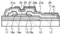
계속해서, 도 2의 일점 쇄선 A-B, C-D에서의 단면도를 도 3에 도시한다. 도 2에 도시하는 트랜지스터(102)는 채널 에치형 트랜지스터이다. 또한, 일점 파선 A-B는, 트랜지스터(102)의 채널 길이 방향, 트랜지스터(102)와 화소 전극으로서 기능하는 도전막(29)의 접속부 및 용량 소자(105)의 단면도이며, C-D에서의 단면도는, 트랜지스터(102)의 채널 폭 방향의 단면도이다.Continuing, cross-sectional views taken along dashed lines A-B and C-D of FIG. 2 are illustrated in FIG. 3. The transistor (102) illustrated in FIG. 2 is a channel etch type transistor. In addition, dashed lines A-B are cross-sectional views of the channel length direction of the transistor (102), the connection portion of the transistor (102) and the conductive film (29) functioning as a pixel electrode, and the capacitor element (105), and the cross-sectional view at C-D is a cross-sectional view of the channel width direction of the transistor (102).
도 3에 도시하는 트랜지스터(102)는, 싱글 게이트 구조의 트랜지스터이며, 기판(11) 위에 설치되는 게이트 전극으로서 기능하는 도전막(13)을 갖는다. 또한, 기판(11) 및 게이트 전극으로서 기능하는 도전막(13) 위에 형성되는 산소에 대한 배리어막(15)과, 산소에 대한 배리어막(15) 위에 형성되는 산화물 절연막(17)과, 산소에 대한 배리어막(15) 및 산화물 절연막(17)을 개재하여, 게이트 전극으로서 기능하는 도전막(13)과 중첩되는 산화물 반도체막(19a)과, 산화물 반도체막(19a)에 접하는, 한 쌍의 전극으로서 기능하는 도전막(21a, 21b)을 갖는다. 또한, 산화물 절연막(17), 산화물 반도체막(19a) 및 한 쌍의 전극으로서 기능하는 도전막(21a, 21b) 위에는, 산화물 절연막(23)이 형성되고, 산화물 절연막(23) 위에는 산화물 절연막(25)이 형성된다. 산소에 대한 배리어막(15), 산화물 절연막(17), 산화물 절연막(23), 산화물 절연막(25), 도전막(21a) 및 도전막(21b) 위에는 산소에 대한 배리어막(27)이 형성된다. 또한, 한 쌍의 전극으로서 기능하는 도전막(21a, 21b) 중 한쪽, 여기서는 도전막(21b)에 접속하는 도전막(29)이, 산소에 대한 배리어막(27) 위에 형성된다. 또한, 도전막(29)은 화소 전극으로서 기능한다.The transistor (102) illustrated in Fig. 3 is a single-gate structure transistor and has a conductive film (13) that functions as a gate electrode and is installed on a substrate (11). In addition, it has a barrier film (15) for oxygen formed on the substrate (11) and the conductive film (13) that functions as a gate electrode, an oxide insulating film (17) formed on the barrier film (15) for oxygen, an oxide semiconductor film (19a) that overlaps the conductive film (13) that functions as a gate electrode with the oxygen barrier film (15) and the oxide insulating film (17) interposed therebetween, and conductive films (21a, 21b) that function as a pair of electrodes that are in contact with the oxide semiconductor film (19a). In addition, an oxide insulating film (23) is formed on the oxide insulating film (17), the oxide semiconductor film (19a), and the conductive films (21a, 21b) functioning as a pair of electrodes, and an oxide insulating film (25) is formed on the oxide insulating film (23). An oxygen barrier film (27) is formed on the oxygen barrier film (15), the oxide insulating film (17), the oxide insulating film (23), the oxide insulating film (25), the conductive film (21a), and the conductive film (21b). In addition, a conductive film (29) connected to one of the conductive films (21a, 21b) functioning as a pair of electrodes, in this case the conductive film (21b), is formed on the oxygen barrier film (27). In addition, the conductive film (29) functions as a pixel electrode.
또한, 도 3에 도시하는 용량 소자(105)는, 산화물 절연막(17) 위에 형성되는 도전성을 갖는 막(19b)과, 산소에 대한 배리어막(27)과, 화소 전극으로서 기능하는 도전막(29)을 갖는다.In addition, the capacitor element (105) illustrated in Fig. 3 has a conductive film (19b) formed on an oxide insulating film (17), a barrier film (27) for oxygen, and a conductive film (29) functioning as a pixel electrode.
본 실시 형태에 나타내는 트랜지스터(102) 위에는 분리된 산화물 절연막(23, 25)이 형성된다. 분리된 산화물 절연막(23, 25)이 산화물 반도체막(19a)과 중첩한다. 또한, 산소에 대한 배리어막(15)과, 산소에 대한 배리어막(27)이, 산화물 반도체막(19a) 및 산화물 절연막(23, 25)을 내측에 가지면서 접하고 있다.A separated oxide insulating film (23, 25) is formed on the transistor (102) shown in this embodiment. The separated oxide insulating film (23, 25) overlaps with the oxide semiconductor film (19a). In addition, a barrier film (15) for oxygen and a barrier film (27) for oxygen are in contact with the oxide semiconductor film (19a) and the oxide insulating film (23, 25) while having them on the inside.
산소에 대한 배리어막(15, 27)은, 산소의 투과성이 낮은 절연막을 사용하는 것이 가능하다. 나아가, 산소, 수소 및 물의 투과성이 낮은 절연막을 사용하는 것이 가능하다. 산소의 투과성이 낮은 절연막, 산소, 수소 및 물의 투과성이 낮은 절연막으로서는, 질화 실리콘막, 질화산화 실리콘막, 질화 알루미늄막, 질화산화 알루미늄막 등의 질화물 절연막이 있다. 또한, 산소의 투과성이 낮은 절연막, 산소, 수소 및 물의 투과성이 낮은 절연막으로서는, 산화 알루미늄막, 산화질화 알루미늄막, 산화 갈륨막, 산화질화 갈륨막, 산화 이트륨막, 산화질화 이트륨막, 산화 하프늄막, 산화질화 하프늄막 등의 산화물 절연막이 있다.As the oxygen barrier film (15, 27), it is possible to use an insulating film having low oxygen permeability. Furthermore, it is possible to use an insulating film having low oxygen, hydrogen, and water permeability. As an insulating film having low oxygen permeability and low oxygen, hydrogen, and water permeability, there are nitride insulating films such as a silicon nitride film, a silicon nitride oxide film, an aluminum nitride film, and an aluminum nitride oxide film. In addition, as an insulating film having low oxygen permeability and low oxygen, hydrogen, and water permeability, there are oxide insulating films such as an aluminum oxide film, an aluminum oxynitride film, a gallium oxide film, a gallium oxynitride film, a yttrium oxide film, an yttrium oxynitride film, a hafnium oxide film, and a hafnium oxynitride film.
산화물 반도체막(19a)은 대표적으로는, In-Ga 산화물막, In-Zn 산화물막, In-M-Zn 산화물막(M은 Al, Ga, Y, Zr, La, Ce 또는 Nd) 등으로 형성된다.The oxide semiconductor film (19a) is typically formed of an In-Ga oxide film, an In-Zn oxide film, an In-M-Zn oxide film (M is Al, Ga, Y, Zr, La, Ce or Nd), etc.
또한, 산화물 반도체막(19a) 위에 설치되는 산화물 절연막(23) 또는 산화물 절연막(25)은, 화학양론적 조성을 만족하는 산소보다 많은 산소를 포함하는 산화물 절연막이다. 화학양론적 조성을 만족하는 산소보다 많은 산소를 포함하는 산화물 절연막은, 가열에 의해 산소의 일부가 탈리된다. 화학양론적 조성을 만족하는 산소보다 많은 산소를 포함하는 산화물 절연막은, TDS 분석에 있어서, 표면 온도가 100℃ 이상 700℃ 이하 또는 100℃ 이상 500℃ 이하의 가열 처리에서의 산소 원자의 탈리량이 1.0×10¹⁸atoms/cm3 이상 또는 3.0×10²⁰atoms/cm3 이상인 산화물 절연막이다.In addition, the oxide insulating film (23) or the oxide insulating film (25) installed on the oxide semiconductor film (19a) is an oxide insulating film that contains more oxygen than oxygen satisfying the stoichiometric composition. The oxide insulating film that contains more oxygen than oxygen satisfying the stoichiometric composition desorbs some of the oxygen by heating. The oxide insulating film that contains more oxygen than oxygen satisfying the stoichiometric composition is an oxide insulating film in which, in TDS analysis, the amount of oxygen atoms desorbed during heat treatment at a surface temperature of 100°C or more and 700°C or less or 100°C or more and 500°C or less is 1.0×10¹⁸ atoms/cm3 or more or 3.0×10²⁰ atoms/cm3 or more.
산화물 절연막(23) 또는 산화물 절연막(25)에 있어서, 화학양론적 조성을 만족하는 산소보다 많은 산소를 포함하는 산화물 절연막이 포함되면, 산화물 절연막(23) 또는 산화물 절연막(25)에 포함되는 산소의 일부를 산화물 반도체막(19a)으로 이동시켜, 산화물 반도체막(19a)에 포함되는 산소 결손을 저감하는 것이 가능하다.In the oxide insulating film (23) or oxide insulating film (25), if an oxide insulating film containing more oxygen than oxygen satisfying the stoichiometric composition is included, it is possible to reduce oxygen vacancies included in the oxide semiconductor film (19a) by moving some of the oxygen included in the oxide insulating film (23) or oxide insulating film (25) to the oxide semiconductor film (19a).
또한, 산소에 대한 배리어막(15)과, 산소에 대한 배리어막(27)이, 산화물 반도체막(19a) 및 산화물 절연막(23, 25)을 내측에 가지면서 접하고 있다.In addition, a barrier film (15) for oxygen and a barrier film (27) for oxygen are in contact with an oxide semiconductor film (19a) and an oxide insulating film (23, 25) on the inside.
산화물 반도체막 중에 산소 결손이 포함되어 있는 산화물 반도체막을 사용한 트랜지스터는, 임계값 전압이 마이너스 방향으로 변동하기 쉬워, 노멀리 온 특성이 되기 쉽다. 이것은, 산화물 반도체막에 포함되는 산소 결손에 기인하여 전하가 발생하여, 저저항화되기 때문이다. 트랜지스터가 노멀리 온 특성을 가지면, 동작 시에 동작 불량이 발생하기 쉬워지거나 또는 비동작 시의 소비 전력이 높아지는 등의 여러 문제가 발생한다. 또한, 경시 변화나 스트레스 시험에 의한, 트랜지스터의 전기 특성, 대표적으로는 임계값 전압의 변동량이 증대한다는 문제가 있다.A transistor using an oxide semiconductor film containing oxygen vacancies in the oxide semiconductor film tends to have a threshold voltage that tends to fluctuate in the negative direction, and thus tends to have normally-on characteristics. This is because charges are generated due to the oxygen vacancies contained in the oxide semiconductor film, resulting in low resistance. If a transistor has normally-on characteristics, various problems occur, such as a tendency for malfunctions to occur during operation or increased power consumption during non-operation. In addition, there is a problem that the amount of variation in the electrical characteristics of the transistor, typically the threshold voltage, increases due to changes over time or stress tests.
그러나, 본 실시 형태에 나타내는 트랜지스터(102)는, 산화물 반도체막(19a) 위에 설치되는 산화물 절연막(23) 또는 산화물 절연막(25)이, 화학양론적 조성을 만족하는 산소보다 많은 산소를 포함하는 산화물 절연막이다. 또한, 산화물 반도체막(19a), 산화물 절연막(23) 및 산화물 절연막(25)을 산소에 대한 배리어막(15) 및 산소에 대한 배리어막(27)으로 감싼다. 그 결과, 산화물 절연막(23) 또는 산화물 절연막(25)에 포함되는 산소가, 효율적으로 산화물 반도체막(19a)으로 이동하여, 산화물 반도체막(19a)의 산소 결손이 저감된다. 그 결과, 노멀리 오프 특성을 갖는 트랜지스터가 된다. 또한, 경시 변화나 스트레스 시험에 의해, 트랜지스터의 전기 특성, 대표적으로는 임계값 전압의 변동량을 저감할 수 있다.However, in the transistor (102) shown in the present embodiment, the oxide insulating film (23) or the oxide insulating film (25) provided on the oxide semiconductor film (19a) is an oxide insulating film that contains more oxygen than oxygen satisfying the stoichiometric composition. In addition, the oxide semiconductor film (19a), the oxide insulating film (23) and the oxide insulating film (25) are surrounded by a barrier film (15) for oxygen and a barrier film (27) for oxygen. As a result, the oxygen contained in the oxide insulating film (23) or the oxide insulating film (25) efficiently moves to the oxide semiconductor film (19a), and the oxygen vacancy of the oxide semiconductor film (19a) is reduced. As a result, a transistor having normally-off characteristics is obtained. In addition, the amount of variation in the electrical characteristics of the transistor, typically the threshold voltage, can be reduced by changes over time or stress tests.
또한, 용량 소자(105)에 있어서, 도전성을 갖는 막(19b)은, 산화물 반도체막(19a)과 동시에 형성된 막이며, 또한 불순물을 포함함으로써 도전성이 높아진 막이다. 또는, 도전성을 갖는 막(19b)은, 산화물 반도체막(19a)과 동시에 형성된 막이며, 또한 불순물을 포함함과 함께, 플라즈마 대미지 등에 의해 산소 결손이 형성되어, 도전성이 높아진 막이다.In addition, in the capacitor element (105), the conductive film (19b) is a film formed simultaneously with the oxide semiconductor film (19a), and is a film whose conductivity is enhanced by including impurities. Alternatively, the conductive film (19b) is a film formed simultaneously with the oxide semiconductor film (19a), and is a film whose conductivity is enhanced by forming oxygen vacancies due to plasma damage or the like, while also including impurities.
본 실시 형태에 나타내는 반도체 장치의 소자 기판은, 트랜지스터의 산화물 반도체막과 동시에, 용량 소자의 한쪽이 되는 전극이 형성된다. 또한, 화소 전극으로서 기능하는 도전막을 용량 소자의 다른 쪽 전극으로서 사용한다. 이 때문에, 용량 소자를 형성하기 위해서, 새롭게 도전막을 형성하는 공정이 불필요하여, 제작 공정을 삭감할 수 있다. 또한, 한 쌍의 전극이 투광성을 갖기 때문에, 용량 소자는 투광성을 갖는다. 그 결과, 용량 소자의 점유 면적을 크게 하면서, 화소의 개구율을 높일 수 있다.The semiconductor device substrate shown in this embodiment has an oxide semiconductor film of a transistor and an electrode that becomes one side of a capacitor element formed at the same time. In addition, a conductive film that functions as a pixel electrode is used as the other electrode of the capacitor element. Therefore, in order to form the capacitor element, a process of forming a new conductive film is unnecessary, and thus the manufacturing process can be reduced. In addition, since one pair of electrodes has light transmitting properties, the capacitor element has light transmitting properties. As a result, the aperture ratio of the pixel can be increased while increasing the occupied area of the capacitor element.
이하에, 트랜지스터(102)의 구성의 상세에 대하여 설명한다.Below, the details of the configuration of the transistor (102) are described.
기판(11)의 재질 등에 큰 제한은 없지만, 적어도, 후의 열처리에 견딜 수 있을 정도의 내열성을 갖고 있을 필요가 있다. 예를 들어, 유리 기판, 세라믹 기판, 석영 기판, 사파이어 기판 등을 기판(11)으로서 사용해도 된다. 또한, 실리콘이나 탄화 실리콘 등의 단결정 반도체 기판, 다결정 반도체 기판, 실리콘 게르마늄 등의 화합물 반도체 기판, SOI 기판 등을 적용하는 것도 가능하고, 이들의 기판 위에 반도체 소자가 설치된 것을 기판(11)으로서 사용해도 된다. 또한, 기판(11)으로서 유리 기판을 사용하는 경우, 제6 세대(1500mm×1850mm), 제7 세대(1870mm×2200mm), 제8 세대(2200mm×2400mm), 제9 세대(2400mm×2800mm), 제10 세대(2950mm×3400mm) 등의 대면적 기판을 사용함으로써 대형의 표시 장치를 제작할 수 있다.There are no major restrictions on the material of the substrate (11), but at least it needs to have heat resistance enough to withstand subsequent heat treatment. For example, a glass substrate, a ceramic substrate, a quartz substrate, a sapphire substrate, etc. may be used as the substrate (11). In addition, it is also possible to apply a single crystal semiconductor substrate such as silicon or silicon carbide, a polycrystal semiconductor substrate, a compound semiconductor substrate such as silicon germanium, an SOI substrate, etc., and a substrate on which a semiconductor element is installed may be used as the substrate (11). In addition, when a glass substrate is used as the substrate (11), a large-area substrate such as the 6th generation (1500 mm × 1850 mm), the 7th generation (1870 mm × 2200 mm), the 8th generation (2200 mm × 2400 mm), the 9th generation (2400 mm × 2800 mm), and the 10th generation (2950 mm × 3400 mm) can be used to manufacture a large display device.
또한, 기판(11)으로서, 가요성 기판을 사용하여, 가요성 기판 위에 직접 트랜지스터(102)를 형성해도 된다. 또는, 기판(11)과 트랜지스터(102) 사이에 박리층을 형성해도 된다. 박리층은, 그 위에 반도체 장치를 일부 또는 전부 완성시킨 후, 기판(11)으로부터 분리하여, 다른 기판에 옮겨 적재하는데 사용할 수 있다. 그때, 트랜지스터(102)는, 내열성이 떨어지는 기판이나 가요성의 기판에도 옮겨 적재할 수 있다.In addition, as the substrate (11), a flexible substrate may be used, and the transistor (102) may be formed directly on the flexible substrate. Alternatively, a peeling layer may be formed between the substrate (11) and the transistor (102). The peeling layer can be used to separate a semiconductor device partially or completely formed thereon from the substrate (11) and transfer and load it onto another substrate. At that time, the transistor (102) can be transferred and loaded onto a substrate with poor heat resistance or a flexible substrate.
게이트 전극으로서 기능하는 도전막(13)은, 알루미늄, 크롬, 구리, 탄탈륨, 티타늄, 몰리브덴, 텅스텐에서 선택된 금속 원소, 또는 상술한 금속 원소를 성분으로 하는 합금이나, 상술한 금속 원소를 조합한 합금 등을 사용하여 형성할 수 있다. 또한, 망간, 지르코늄 중 어느 하나 또는 복수에서 선택된 금속 원소를 사용해도 된다. 또한, 게이트 전극으로서 기능하는 도전막(13)은, 단층 구조나 2층 이상의 적층 구조로 해도 된다. 예를 들어, 실리콘을 포함하는 알루미늄막의 단층 구조, 티타늄막 위에 알루미늄막을 적층하는 2층 구조, 질화티타늄막 위에 티타늄막을 적층하는 2층 구조, 질화티타늄막 위에 텅스텐막을 적층하는 2층 구조, 질화 탄탈막 또는 질화 텅스텐막 위에 텅스텐막을 적층하는 2층 구조, 티타늄막 위에 구리막을 적층하는 2층 구조, 티타늄막과, 그 티타늄막 위에 알루미늄막을 적층하고, 또한 그 위에 티타늄막을 형성하는 3층 구조 등이 있다. 또한, 알루미늄에, 티타늄, 탄탈륨, 텅스텐, 몰리브덴, 크롬, 네오디뮴, 스칸듐에서 선택된 원소의 막 또는 복수 조합한 합금막, 또는 질화막을 사용해도 된다.The conductive film (13) functioning as a gate electrode can be formed using a metal element selected from aluminum, chromium, copper, tantalum, titanium, molybdenum, and tungsten, or an alloy containing the above-described metal elements as a component, or an alloy combining the above-described metal elements. In addition, a metal element selected from one or more of manganese and zirconium may be used. In addition, the conductive film (13) functioning as a gate electrode may have a single-layer structure or a laminated structure of two or more layers. For example, there are a single-layer structure of an aluminum film containing silicon, a two-layer structure in which an aluminum film is laminated on a titanium film, a two-layer structure in which a titanium film is laminated on a titanium nitride film, a two-layer structure in which a tungsten film is laminated on a titanium nitride film, a two-layer structure in which a tungsten film is laminated on a tantalum nitride film or a tungsten nitride film, a two-layer structure in which a copper film is laminated on a titanium film, a three-layer structure in which a titanium film, an aluminum film is laminated on the titanium film, and a titanium film is further formed thereon, etc. In addition, a film of an element selected from titanium, tantalum, tungsten, molybdenum, chromium, neodymium, and scandium, an alloy film combining multiple elements, or a nitride film may be used on aluminum.
또한, 게이트 전극으로서 기능하는 도전막(13)은, 인듐 주석 산화물, 산화텅스텐을 포함하는 인듐 산화물, 산화텅스텐을 포함하는 인듐 아연 산화물, 산화티타늄을 포함하는 인듐 산화물, 산화티타늄을 포함하는 인듐 주석 산화물, 인듐 아연 산화물, 산화 실리콘을 첨가한 인듐 주석 산화물 등의 투광성을 갖는 도전성 재료를 적용할 수도 있다. 또한, 상기 투광성을 갖는 도전성 재료와, 상기 금속 원소의 적층 구조로 할 수도 있다.In addition, the conductive film (13) functioning as a gate electrode may use a light-transmitting conductive material such as indium tin oxide, indium oxide containing tungsten oxide, indium zinc oxide containing tungsten oxide, indium oxide containing titanium oxide, indium tin oxide containing titanium oxide, indium zinc oxide, or indium tin oxide with added silicon oxide. In addition, it may be formed into a layered structure of the light-transmitting conductive material and the metal element.
산소에 대한 배리어막(15)은, 산소의 투과성이 낮은 절연막을 사용하는 것이 가능하다. 나아가, 산소, 수소 및 물의 투과성이 낮은 절연막을 사용하는 것이 가능하다. 산소의 투과성이 낮은 절연막, 산소, 수소 및 물의 투과성이 낮은 절연막으로서는, 질화 실리콘막, 질화산화 실리콘막, 질화 알루미늄막, 질화산화 알루미늄막 등의 질화물 절연막이 있다. 또한, 산소의 투과성이 낮은 절연막, 산소, 수소 및 물의 투과성이 낮은 절연막으로서는, 산화 알루미늄막, 산화질화 알루미늄막, 산화 갈륨막, 산화질화 갈륨막, 산화 이트륨막, 산화질화 이트륨막, 산화 하프늄막, 산화질화 하프늄막 등의 산화물 절연막이 있다.As the barrier film (15) for oxygen, it is possible to use an insulating film having low oxygen permeability. Furthermore, it is possible to use an insulating film having low oxygen, hydrogen, and water permeability. As an insulating film having low oxygen permeability and low oxygen, hydrogen, and water permeability, there are nitride insulating films such as a silicon nitride film, a silicon nitride oxide film, an aluminum nitride film, and an aluminum nitride oxide film. In addition, as an insulating film having low oxygen permeability and low oxygen, hydrogen, and water permeability, there are oxide insulating films such as an aluminum oxide film, an aluminum oxynitride film, a gallium oxide film, a gallium oxynitride film, an yttrium oxide film, an yttrium oxynitride film, a hafnium oxide film, and a hafnium oxynitride film.
산소에 대한 배리어막(15)의 두께는, 5nm 이상 100nm 이하 또는 20nm 이상 80nm 이하로 하면 된다.The thickness of the barrier film (15) for oxygen may be 5 nm or more and 100 nm or less, or 20 nm or more and 80 nm or less.
산화물 절연막(17)은, 예를 들어 산화 실리콘, 산화질화 실리콘, 산화 알루미늄, 산화 하프늄, 산화 갈륨 또는 Ga-Zn계 금속 산화물 등을 사용하면 되고, 적층 또는 단층으로 설치한다.The oxide insulating film (17) may be made of, for example, silicon oxide, silicon nitride oxide, aluminum oxide, hafnium oxide, gallium oxide, or Ga-Zn metal oxide, and is installed in a laminated or single layer form.
또한, 산화물 절연막(17)으로서, 하프늄 실리케이트(HfSiOx), 질소가 첨가 된 하프늄 실리케이트(HfSixOyNz), 질소가 첨가된 하프늄 알루미네이트(HfAlxOyNz), 산화 하프늄, 산화 이트륨 등의 high-k 재료를 사용함으로써 트랜지스터의 게이트 누설을 저감할 수 있다.In addition, by using a high-k material such as hafnium silicate (HfSiOx ), nitrogen-doped hafnium silicate (HfSix Oy Nz ), nitrogen-doped hafnium aluminate (HfAlx Oy Nz ), hafnium oxide, or yttrium oxide as an oxide insulating film (17), the gate leakage of the transistor can be reduced.
산화물 절연막(17)의 두께는, 5nm 이상 400nm 이하, 10nm 이상 300nm 이하 또는 50nm 이상 250nm 이하로 하면 된다.The thickness of the oxide insulating film (17) may be 5 nm or more and 400 nm or less, 10 nm or more and 300 nm or less, or 50 nm or more and 250 nm or less.
산화물 반도체막(19a)은 대표적으로는, In-Ga 산화물, In-Zn 산화물, In-M-Zn 산화물(M은 Al, Ga, Y, Zr, La, Ce 또는 Nd)을 사용하여 형성한다.The oxide semiconductor film (19a) is typically formed using In-Ga oxide, In-Zn oxide, or In-M-Zn oxide (M is Al, Ga, Y, Zr, La, Ce, or Nd).
또한, 산화물 반도체막(19a)이 In-M-Zn 산화물막일 때, In 및 M의 합을 100 atomic%로 했을 경우, In과 M의 원자수 비율은 In이 25 atomic% 이상 및 M이 75 atomic% 미만 또는 In이 34 atomic% 이상 및 M이 66 atomic% 미만으로 한다.In addition, when the oxide semiconductor film (19a) is an In-M-Zn oxide film, when the sum of In and M is 100 atomic%, the atomic ratio of In and M is set to be 25 atomic% or more for In and less than 75 atomic% for M, or 34 atomic% or more for In and less than 66 atomic% for M.
산화물 반도체막(19a)은, 에너지 갭이 2eV 이상, 2.5eV 이상 또는 3eV 이상이다. 이와 같이, 에너지 갭이 넓은 산화물 반도체를 사용함으로써 트랜지스터(102)의 오프 전류를 저감할 수 있다.The oxide semiconductor film (19a) has an energy gap of 2 eV or more, 2.5 eV or more, or 3 eV or more. In this way, by using an oxide semiconductor having a wide energy gap, the off-state current of the transistor (102) can be reduced.
산화물 반도체막(19a)의 두께는, 3nm 이상 200nm 이하, 3nm 이상 100nm 이하 또는 3nm 이상 50nm 이하로 한다.The thickness of the oxide semiconductor film (19a) is set to 3 nm or more and 200 nm or less, 3 nm or more and 100 nm or less, or 3 nm or more and 50 nm or less.
산화물 반도체막(19a)이 In-M-Zn 산화물막(M은 Al, Ga, Y, Zr, La, Ce 또는 Nd)인 경우, In-M-Zn 산화물막을 성막하기 위해 사용하는 스퍼터링 타깃의 금속 원소의 원자수비는, In≥M, Zn≥M을 만족하는 것이 바람직하다. 이러한 스퍼터링 타깃의 금속 원소의 원자수비로서, In:M:Zn=1:1:1, In:M:Zn=1:1:1.2, In:M:Zn=3:1:2가 바람직하다. 또한, 성막되는 산화물 반도체막(19a)의 원자수비는 각각, 오차로서 상기의 스퍼터링 타깃에 포함되는 금속 원소의 원자수비의 ±40%의 변동을 포함한다.When the oxide semiconductor film (19a) is an In-M-Zn oxide film (M is Al, Ga, Y, Zr, La, Ce or Nd), it is preferable that the atomic ratio of the metal elements of the sputtering target used to form the In-M-Zn oxide film satisfies In≥M, Zn≥M. As the atomic ratio of the metal elements of this sputtering target, In:M:Zn=1:1:1, In:M:Zn=1:1:1.2, In:M:Zn=3:1:2. In addition, the atomic ratio of the oxide semiconductor film (19a) to be formed includes a variation of ±40% of the atomic ratio of the metal elements included in the sputtering target as an error.
산화물 반도체막(19a)으로서는, 캐리어 밀도가 낮은 산화물 반도체막을 사용한다. 예를 들어, 산화물 반도체막(19a)은, 캐리어 밀도가 1×10¹⁷개/cm3 이하, 1×10¹⁵개/cm3 이하, 1×10¹³개/cm3 이하 또는 1×10¹¹개/cm3 이하의 산화물 반도체막을 사용한다.As the oxide semiconductor film (19a), an oxide semiconductor film having a low carrier density is used. For example, as the oxide semiconductor film (19a), an oxide semiconductor film having a carrier density of 1×10¹⁷ /cm3 or less, 1×10¹⁵ /cm3 or less, 1×10¹³ /cm3 or less, or 1×10¹¹ /cm3 or less is used.
또한, 이들에 한정되지 않고, 필요로 하는 트랜지스터의 반도체 특성 및 전기 특성(전계 효과 이동도, 임계값 전압 등)에 따라서 적절한 조성의 것을 사용하면 된다. 또한, 필요로 하는 트랜지스터의 반도체 특성을 얻기 위해서, 산화물 반도체막(19a)의 캐리어 밀도나 불순물 농도, 결함 밀도, 금속 원소와 산소의 원자수비, 원자간 거리, 밀도 등을 적절한 것으로 하는 것이 바람직하다.In addition, without being limited to these, a composition of an appropriate composition may be used depending on the semiconductor characteristics and electrical characteristics (field effect mobility, threshold voltage, etc.) of the required transistor. In addition, in order to obtain the semiconductor characteristics of the required transistor, it is preferable to make the carrier density, impurity concentration, defect density, atomic ratio of metal elements and oxygen, interatomic distance, density, etc. of the oxide semiconductor film (19a) appropriate.
또한, 산화물 반도체막(19a)으로서, 불순물 농도가 낮고, 결함 준위 밀도가 낮은 산화물 반도체막을 사용함으로써, 더욱 우수한 전기 특성을 갖는 트랜지스터를 제작할 수 있어 바람직하다. 여기에서는, 불순물 농도가 낮고, 결함 준위 밀도가 낮은(산소 결손이 적은) 것을 고순도 진성 또는 실질적으로 고순도 진성이라고 부른다. 고순도 진성 또는 실질적으로 고순도 진성인 산화물 반도체는, 캐리어 발생원이 적기 때문에, 캐리어 밀도를 낮게 할 수 있는 경우가 있다. 따라서, 당해 산화물 반도체막에 채널 영역이 형성되는 트랜지스터는, 임계값 전압이 마이너스가 되는 전기 특성(노멀리 온이라고도 함)으로 되는 경우가 적다. 또한, 고순도 진성 또는 실질적으로 고순도 진성인 산화물 반도체막은, 결함 준위 밀도가 낮기 때문에, 트랩 준위 밀도도 낮아지는 경우가 있다. 또한, 고순도 진성 또는 실질적으로 고순도 진성인 산화물 반도체막은, 오프 전류가 현저하게 작고, 채널 폭이 1×10⁶㎛이고 채널 길이(L)가 10㎛인 소자라도, 소스 전극과 드레인 전극간의 전압(드레인 전압)이 1V 내지 10V의 범위에서, 오프 전류가, 반도체 파라미터 애널라이저의 측정 한계 이하, 즉 1×10-13A 이하라는 특성을 얻을 수 있다. 따라서, 당해 산화물 반도체막에 채널 영역이 형성되는 트랜지스터는, 전기 특성의 변동이 작아, 신뢰성이 높은 트랜지스터가 되는 경우가 있다. 또한, 산화물 반도체막의 트랩 준위에 포획된 전하는, 소실될 때까지 필요한 시간이 길어, 마치 고정 전하와 같이 행동하는 경우가 있다. 그로 인해, 트랩 준위 밀도가 높은 산화물 반도체막에 채널 영역이 형성되는 트랜지스터는, 전기 특성이 불안정해지는 경우가 있다. 불순물로서는, 수소, 질소, 알칼리 금속 또는 알칼리 토금속 등이 있다.In addition, by using an oxide semiconductor film (19a) having a low impurity concentration and a low defect state density, it is preferable to manufacture a transistor having even better electrical characteristics. Here, a film having a low impurity concentration and a low defect state density (few oxygen vacancies) is called a high-purity intrinsic film or a substantially high-purity intrinsic film. Since a high-purity intrinsic film or a substantially high-purity intrinsic film has few carrier generation sources, the carrier density can sometimes be low. Therefore, a transistor in which a channel region is formed in the oxide semiconductor film rarely has an electrical characteristic in which the threshold voltage becomes negative (also called normally on). In addition, since a high-purity intrinsic film or a substantially high-purity intrinsic film has a low defect state density, the trap state density can also sometimes be low. In addition, a high-purity intrinsic or substantially high-purity intrinsic oxide semiconductor film has a remarkably small off-state current, and even in a device having a channel width of 1×10⁶ ㎛ and a channel length (L) of 10 ㎛, the off-state current can obtain the characteristic that it is below the measurement limit of the semiconductor parameter analyzer, that is, 1×10-13 A or less, when the voltage between the source electrode and the drain electrode (drain voltage) is in the range of 1 V to 10 V. Therefore, a transistor in which a channel region is formed in the oxide semiconductor film may have small fluctuations in electrical characteristics and may be a highly reliable transistor. In addition, charges trapped in the trap levels of the oxide semiconductor film may require a long time to disappear, and may behave as if they were fixed charges. Therefore, a transistor in which a channel region is formed in an oxide semiconductor film having a high trap state density may have unstable electrical characteristics. Impurities include hydrogen, nitrogen, an alkali metal, or an alkaline earth metal.
산화물 반도체막에 포함되는 수소는 금속 원자와 결합하는 산소와 반응하여 물이 됨과 함께, 산소가 탈리된 격자(또는 산소가 탈리된 부분)에 산소 결손이 형성된다. 당해 산소 결손에 수소가 들어감으로써, 캐리어인 전자가 생성되는 경우가 있다. 또한, 수소의 일부가 금속 원자와 결합하는 산소와 결합함으로써, 캐리어인 전자를 생성하는 경우가 있다. 따라서, 수소가 포함되어 있는 산화물 반도체를 사용한 트랜지스터는 노멀리 온 특성이 되기 쉽다.Hydrogen contained in an oxide semiconductor film reacts with oxygen that bonds with metal atoms to form water, and oxygen vacancies are formed in the lattice from which oxygen is removed (or the portion from which oxygen is removed). When hydrogen enters the oxygen vacancy, electrons, which are carriers, are sometimes generated. In addition, when some of the hydrogen bonds with oxygen that bonds with metal atoms, electrons, which are carriers, are sometimes generated. Therefore, a transistor using an oxide semiconductor containing hydrogen tends to have normally-on characteristics.
이로 인해, 산화물 반도체막(19a)은 산소 결손과 함께, 수소가 가능한 한 저감되어 있는 것이 바람직하다. 구체적으로는, 산화물 반도체막(19a)에 있어서, 2차 이온 질량 분석법(SIMS: Secondary Ion Mass Spectrometry)에 의해 얻어지는 수소 농도를, 5×10¹⁹atoms/cm3 이하, 1×10¹⁹atoms/cm3 이하, 5×10¹⁸atoms/cm3 이하, 1×10¹⁸atoms/cm3 이하, 5×10¹⁷atoms/cm3 이하 또는 1×10¹⁶atoms/cm3 이하로 한다.For this reason, it is preferable that the oxide semiconductor film (19a) have as little hydrogen as possible along with oxygen vacancies. Specifically, in the oxide semiconductor film (19a), the hydrogen concentration obtained by secondary ion mass spectrometry (SIMS) is set to 5×10¹⁹ atoms/cm3 or less, 1×10¹⁹ atoms/cm3 or less, 5×10¹⁸ atoms/cm3 or less, 1×10¹⁸ atoms/cm3 or less, 5×10¹⁷ atoms/cm3 or less, or 1×10¹⁶ atoms/cm3 or less.
산화물 반도체막(19a)에 있어서, 제14족 원소의 하나인 실리콘이나 탄소가 포함되면, 산화물 반도체막(19a)에서 산소 결손이 증가하여, n형화된다. 이로 인해, 산화물 반도체막(19a)에서의 실리콘이나 탄소의 농도(2차 이온 질량 분석법에 의해 얻어지는 농도)를 2×10¹⁸atoms/cm3 이하 또는 2×10¹⁷atoms/cm3 이하로 한다.In the oxide semiconductor film (19a), if silicon or carbon, which is one of the
또한, 산화물 반도체막(19a)에 있어서, 2차 이온 질량 분석법에 의해 얻어지는 알칼리 금속 또는 알칼리 토금속의 농도를, 1×10¹⁸atoms/cm3 이하 또는 2×10¹⁶atoms/cm3 이하로 한다. 알칼리 금속 및 알칼리 토금속은, 산화물 반도체와 결합하면 캐리어를 생성하는 경우가 있어, 트랜지스터의 오프 전류가 증대되어버리는 경우가 있다. 이로 인해, 산화물 반도체막(19a)의 알칼리 금속 또는 알칼리 토금속의 농도를 저감하는 것이 바람직하다.In addition, in the oxide semiconductor film (19a), the concentration of the alkali metal or alkaline earth metal obtained by secondary ion mass spectrometry is set to 1×10¹⁸ atoms/cm3 or less or 2×10¹⁶ atoms/cm3 or less. When the alkali metal or alkaline earth metal combines with the oxide semiconductor, there are cases where it generates a carrier, and the off-state current of the transistor may increase. Therefore, it is desirable to reduce the concentration of the alkali metal or alkaline earth metal in the oxide semiconductor film (19a).
또한, 산화물 반도체막(19a)에 질소가 포함되어 있으면, 캐리어인 전자가 발생하여, 캐리어 밀도가 증가하고, n형화되기 쉽다. 그 결과, 질소가 포함되어 있는 산화물 반도체를 사용한 트랜지스터는 노멀리 온 특성이 되기 쉽다. 따라서, 당해 산화물 반도체막에 있어서, 질소는 가능한 한 저감되어 있는 것이 바람직하다. 예를 들어 2차 이온 질량 분석법에 의해 얻어지는 질소 농도는, 5×10¹⁸atoms/cm3 이하로 하는 것이 바람직하다.In addition, if nitrogen is included in the oxide semiconductor film (19a), electrons as carriers are generated, the carrier density increases, and it is easy to become n-type. As a result, a transistor using an oxide semiconductor containing nitrogen is easy to have normally-on characteristics. Therefore, in the oxide semiconductor film, it is desirable that nitrogen be reduced as much as possible. For example, the nitrogen concentration obtained by secondary ion mass spectrometry is preferably 5×10¹⁸ atoms/cm3 or less.
또한, 산화물 반도체막(19a)은, 예를 들어 비단결정 구조이어도 된다. 비단결정 구조는, 예를 들어 후술하는 CAAC-OS(C Axis Aligned-Crystalline Oxide Semiconductor), 다결정 구조, 후술하는 미결정 구조 또는 비정질 구조를 포함한다. 비단결정 구조에 있어서, 비정질 구조는 가장 결함 준위 밀도가 높고, CAAC-OS는 가장 결함 준위 밀도가 낮다.In addition, the oxide semiconductor film (19a) may be, for example, a non-single-crystal structure. The non-single-crystal structure includes, for example, a CAAC-OS (C Axis Aligned-Crystalline Oxide Semiconductor) described later, a polycrystalline structure, a microcrystalline structure described later, or an amorphous structure. In the non-single-crystal structure, the amorphous structure has the highest density of defect states, and the CAAC-OS has the lowest density of defect states.
산화물 반도체막(19a)은, 예를 들어 비정질 구조이어도 된다. 비정질 구조의 산화물 반도체막은, 예를 들어 원자 배열이 무질서하며, 결정 성분을 갖지 않는다. 또는, 비정질 구조의 산화물막은, 예를 들어 완전한 비정질 구조이며, 결정부를 갖지 않는다.The oxide semiconductor film (19a) may have, for example, an amorphous structure. An oxide semiconductor film having an amorphous structure has, for example, a disordered atomic arrangement and does not have a crystalline component. Alternatively, an oxide semiconductor film having an amorphous structure has, for example, a completely amorphous structure and does not have a crystalline portion.
또한, 산화물 반도체막(19a)이, 비정질 구조의 영역, 미결정 구조의 영역, 다결정 구조의 영역, CAAC-OS의 영역, 단결정 구조의 영역의 2종 이상을 갖는 혼합막이어도 된다. 혼합막은, 예를 들어 비정질 구조의 영역, 미결정 구조의 영역, 다결정 구조의 영역, CAAC-OS의 영역, 단결정 구조의 영역 중 어느 2종 이상의 영역을 갖는 경우가 있다. 또한, 혼합막은, 예를 들어 비정질 구조의 영역, 미결정 구조의 영역, 다결정 구조의 영역, CAAC-OS의 영역, 단결정 구조의 영역 중 어느 2종 이상의 영역의 적층 구조를 갖는 경우가 있다.In addition, the oxide semiconductor film (19a) may be a mixed film having two or more types of regions including an amorphous structure region, a microcrystalline structure region, a polycrystalline structure region, a CAAC-OS region, and a single crystal structure region. The mixed film may have, for example, two or more types of regions including an amorphous structure region, a microcrystalline structure region, a polycrystalline structure region, a CAAC-OS region, and a single crystal structure region. In addition, the mixed film may have, for example, a stacked structure of two or more types of regions including an amorphous structure region, a microcrystalline structure region, a polycrystalline structure region, a CAAC-OS region, and a single crystal structure region.
도전성을 갖는 막(19b)은, 산화물 반도체막(19a)과 동시에 형성된 산화물 반도체막을 가공하여 형성된다. 이로 인해, 도전성을 갖는 막(19b)은, 산화물 반도체막(19a)과 마찬가지의 금속 원소를 갖는 막이다. 또한, 산화물 반도체막(19a)과 마찬가지의 결정 구조, 또는 상이한 결정 구조를 갖는 막이다. 그러나, 산화물 반도체막(19a)과 동시에 형성된 산화물 반도체막에, 불순물 또는 산소 결손을 갖게 함으로써, 도전성을 갖는 막(19b)이 된다. 산화물 반도체막에 포함되는 불순물로서는 수소가 있다. 또한, 수소 대신에 불순물로서, 붕소, 인, 주석, 안티몬, 희가스 원소, 알칼리 금속, 알칼리 토금속 등이 포함되어 있어도 된다.The conductive film (19b) is formed by processing the oxide semiconductor film formed simultaneously with the oxide semiconductor film (19a). Therefore, the conductive film (19b) is a film having the same metal element as the oxide semiconductor film (19a). In addition, it is a film having the same crystal structure as the oxide semiconductor film (19a) or a different crystal structure. However, by providing an impurity or an oxygen vacancy in the oxide semiconductor film formed simultaneously with the oxide semiconductor film (19a), the conductive film (19b) is formed. Hydrogen is an impurity included in the oxide semiconductor film. In addition, instead of hydrogen, boron, phosphorus, tin, antimony, a rare gas element, an alkali metal, an alkaline earth metal, or the like may be included as an impurity.
이로 인해, 산화물 반도체막(19a) 및 도전성을 갖는 막(19b)은 모두 산화물 절연막(17) 위에 형성되지만, 불순물 농도가 상이하다. 구체적으로는, 산화물 반도체막(19a)과 비교하여, 도전성을 갖는 막(19b)의 불순물 농도가 높다. 예를 들어, 산화물 반도체막(19a)에 포함되는 수소 농도는, 5×10¹⁹atoms/cm3 이하, 5×10¹⁸atoms/cm3 이하, 1×10¹⁸atoms/cm3 이하, 5×10¹⁷atoms/cm3 이하 또는 1×10¹⁶atoms/cm3 이하이고, 도전성을 갖는 막(19b)이 포함되는 수소 농도는, 8×10¹⁹atoms/cm3 이상, 1×10²⁰atoms/cm3 이상 또는 5×10²⁰atoms/cm3 이상이다. 또한, 산화물 반도체막(19a)과 비교하여, 도전성을 갖는 막(19b)에 포함되는 수소 농도는 2배 또는 10배 이상이다.Due to this, both the oxide semiconductor film (19a) and the conductive film (19b) are formed on the oxide insulating film (17), but have different impurity concentrations. Specifically, the impurity concentration of the conductive film (19b) is higher than that of the oxide semiconductor film (19a). For example, the hydrogen concentration included in the oxide semiconductor film (19a) is 5×10¹⁹ atoms/cm3 or less, 5×10¹⁸ atoms/cm3 or less, 1×10¹⁸ atoms/cm3 or less, 5×10¹⁷ atoms/cm3 or less, or 1×10¹⁶ atoms/cm3 or less, and the hydrogen concentration included in the conductive film (19b) is 8×10¹⁹ atoms/cm3 or more, 1×10²⁰ atoms/cm3 or more, or 5×10²⁰ atoms/cm3 or more. In addition, compared to the oxide semiconductor film (19a), the hydrogen concentration included in the conductive film (19b) is 2 times or 10 times or more.
또한, 산화물 반도체막(19a)과 동시에 형성된 산화물 반도체막을 플라즈마에 노출시킴으로써, 산화물 반도체막에 대미지를 미쳐, 산소 결손을 형성할 수 있다. 예를 들어, 산화물 반도체막 위에, 플라즈마 CVD법 또는 스퍼터링법으로 막을 성막하면, 산화물 반도체막이 플라즈마에 노출되어, 산소 결손이 생성된다. 또는, 산화물 절연막(23) 및 산화물 절연막(25)을 형성하기 위한 에칭 처리에 있어서 산화물 반도체막이 플라즈마에 노출됨으로써, 산소 결손이 생성된다. 또는, 산화물 반도체막이, 산소 및 수소의 혼합 가스, 수소, 희가스, 암모니아 등의 플라즈마에 노출됨으로써, 산소 결손이 생성된다. 그 결과, 산화물 반도체막은 도전성이 높아져서, 도전성을 갖는 막(19b)이 된다.In addition, by exposing the oxide semiconductor film formed simultaneously with the oxide semiconductor film (19a) to plasma, the oxide semiconductor film can be damaged to form oxygen vacancies. For example, when a film is formed on the oxide semiconductor film by plasma CVD or sputtering, the oxide semiconductor film is exposed to plasma, and oxygen vacancies are generated. Alternatively, when the oxide semiconductor film is exposed to plasma during the etching process for forming the oxide insulating film (23) and the oxide insulating film (25), oxygen vacancies are generated. Alternatively, the oxide semiconductor film is exposed to plasma, such as a mixed gas of oxygen and hydrogen, hydrogen, a noble gas, or ammonia, and oxygen vacancies are generated. As a result, the oxide semiconductor film becomes highly conductive, and becomes a conductive film (19b).
즉, 도전성을 갖는 막(19b)은, 도전성이 높은 산화물 반도체막이라고도 할 수 있다. 또한, 도전성을 갖는 막(19b)은, 도전성이 높은 금속 산화물막이라고도 할 수 있다.That is, the conductive film (19b) can also be called a highly conductive oxide semiconductor film. In addition, the conductive film (19b) can also be called a highly conductive metal oxide film.
또한, 산소에 대한 배리어막(27)으로서 질화 실리콘막을 사용하는 경우, 질화 실리콘막은 수소를 포함한다. 이로 인해, 산소에 대한 배리어막(27)의 수소가 산화물 반도체막(19a)과 동시에 형성된 산화물 반도체막에 확산되면, 해당 산화물 반도체막에 있어서 수소는 산소와 결합하여, 캐리어인 전자가 생성된다. 또한, 산소에 대한 배리어막(27)으로서, 질화 실리콘막을 플라즈마 CVD법 또는 스퍼터링 법으로 성막하면, 산화물 반도체막이 플라즈마에 노출되어, 산소 결손이 생성된다. 당해 산소 결손에, 질화 실리콘막에 포함되는 수소가 들어감으로써, 캐리어인 전자가 생성된다. 그 결과, 산화물 반도체막은 도전성이 높아져서, 도전성을 갖는 막(19b)이 된다.In addition, when a silicon nitride film is used as a barrier film (27) for oxygen, the silicon nitride film contains hydrogen. Therefore, when hydrogen of the barrier film (27) for oxygen is diffused into the oxide semiconductor film formed at the same time as the oxide semiconductor film (19a), hydrogen combines with oxygen in the oxide semiconductor film, and electrons, which are carriers, are generated. In addition, when a silicon nitride film is formed as a barrier film (27) for oxygen by a plasma CVD method or a sputtering method, the oxide semiconductor film is exposed to plasma, and oxygen vacancies are generated. When hydrogen contained in the silicon nitride film enters the oxygen vacancies, electrons, which are carriers, are generated. As a result, the oxide semiconductor film has high conductivity, and becomes a conductive film (19b).
도전성을 갖는 막(19b)은 산화물 반도체막(19a)보다 저항률이 낮다. 도전성을 갖는 막(19b)의 저항률이, 산화물 반도체막(19a)의 저항률에 1×10⁻⁸배 이상 1×10⁻¹배 미만인 것이 바람직하고, 대표적으로는 1×10⁻³Ωcm 이상 1×10⁴Ωcm 미만 또는 저항률이 1×10⁻³Ωcm 이상 1×10⁻¹Ωcm 미만이면 된다.The conductive film (19b) has a lower resistivity than the oxide semiconductor film (19a). It is preferable that the resistivity of the conductive film (19b) be 1×10⁻⁸ times or more and less than 1×10⁻¹ times the resistivity of the oxide semiconductor film (19a), and typically, it is 1×10⁻³ Ωcm or more and less than 1×10⁴ Ωcm, or the resistivity is 1×10⁻³ Ωcm or more and less than 1×10⁻¹ Ωcm.
한 쌍의 전극으로서 기능하는 도전막(21a, 21b)은, 알루미늄, 티타늄, 크롬, 니켈, 구리, 이트륨, 지르코늄, 몰리브덴, 은, 탄탈륨 또는 텅스텐을 포함하는 단체 금속, 또는 이것을 주성분으로 하는 합금을 단층 구조 또는 적층 구조로서 사용한다. 예를 들어, 실리콘을 포함하는 알루미늄막의 단층 구조, 티타늄막 위에 알루미늄막을 적층하는 2층 구조, 텅스텐막 위에 알루미늄막을 적층하는 2층 구조, 구리-마그네슘-알루미늄 합금막 위에 구리막을 적층하는 2층 구조, 티타늄막 위에 구리막을 적층하는 2층 구조, 텅스텐막 위에 구리막을 적층하는 2층 구조, 티타늄막 또는 질화 티타늄막과, 그 티타늄막 또는 질화 티타늄막 위에 중첩하여 알루미늄막 또는 구리막을 적층하고, 또한 그 위에 티타늄막 또는 질화 티타늄막을 형성하는 3층 구조, 몰리브덴막 또는 질화 몰리브덴막과, 그 몰리브덴막 또는 질화 몰리브덴막 위에 중첩하여 알루미늄막 또는 구리막을 적층하고, 또한 그 위에 몰리브덴막 또는 질화 몰리브덴막을 형성하는 3층 구조 등이 있다. 또한, 산화인듐, 산화주석 또는 산화아연을 포함하는 투명 도전 재료를 사용해도 된다.The conductive film (21a, 21b) functioning as a pair of electrodes uses a single metal including aluminum, titanium, chromium, nickel, copper, yttrium, zirconium, molybdenum, silver, tantalum or tungsten, or an alloy containing these as a main component, in a single-layer structure or a laminated structure. For example, there are a single-layer structure of an aluminum film containing silicon, a two-layer structure in which an aluminum film is laminated on a titanium film, a two-layer structure in which an aluminum film is laminated on a tungsten film, a two-layer structure in which a copper film is laminated on a copper-magnesium-aluminum alloy film, a two-layer structure in which a copper film is laminated on a titanium film, a two-layer structure in which a copper film is laminated on a tungsten film, a three-layer structure in which a titanium film or a titanium nitride film is laminated with an aluminum or copper film overlapping the titanium film or the titanium nitride film, and a titanium film or a titanium nitride film is further formed thereon, a three-layer structure in which a molybdenum film or a molybdenum nitride film is laminated with an aluminum or copper film overlapping the molybdenum film or the molybdenum nitride film, and a molybdenum film or molybdenum nitride film is further formed thereon, etc. In addition, a transparent conductive material containing indium oxide, tin oxide, or zinc oxide may be used.
산화물 절연막(23) 또는 산화물 절연막(25)으로서, 화학양론적 조성을 만족하는 산소보다 많은 산소를 포함하는 산화물 절연막을 사용하는 것이 바람직하다. 여기에서는, 산화물 절연막(23)으로서, 산소를 투과하는 산화물 절연막을 형성하고, 산화물 절연막(25)으로서, 화학양론적 조성을 만족하는 산소보다 많은 산소를 포함하는 산화물 절연막을 형성한다.As the oxide insulating film (23) or oxide insulating film (25), it is preferable to use an oxide insulating film that contains more oxygen than the oxygen satisfying the stoichiometric composition. Here, as the oxide insulating film (23), an oxide insulating film that permeates oxygen is formed, and as the oxide insulating film (25), an oxide insulating film that contains more oxygen than the oxygen satisfying the stoichiometric composition is formed.
산화물 절연막(23)은, 산소를 투과하는 산화물 절연막이다. 이로 인해, 산화물 절연막(23) 위에 설치되는 산화물 절연막(25)으로부터 탈리되는 산소를, 산화물 절연막(23)을 통해 산화물 반도체막(19a)으로 이동시킬 수 있다. 또한, 산화물 절연막(23)은, 후에 형성하는 산화물 절연막(25)을 형성할 때의, 산화물 반도체막(19a)에 대한 대미지 완화막으로서도 기능한다.The oxide insulating film (23) is an oxide insulating film that is permeable to oxygen. Due to this, oxygen released from the oxide insulating film (25) provided on the oxide insulating film (23) can be moved to the oxide semiconductor film (19a) through the oxide insulating film (23). In addition, the oxide insulating film (23) also functions as a damage mitigating film for the oxide semiconductor film (19a) when forming the oxide insulating film (25) that is formed later.
산화물 절연막(23)으로서는, 두께가 5nm 이상 150nm 이하 또는 5nm 이상 50nm 이하의 산화 실리콘막, 산화질화 실리콘막 등을 사용할 수 있다. 또한, 본 명세서 중에서, 산화질화 실리콘막이란, 그 조성으로서, 질소보다 산소의 함유량이 많은 막을 가리키고, 질화산화 실리콘막이란, 그 조성으로서, 산소보다 질소의 함유량이 많은 막을 가리킨다.As the oxide insulating film (23), a silicon oxide film, a silicon oxynitride film, etc., having a thickness of 5 nm or more and 150 nm or less, or 5 nm or more and 50 nm or less, can be used. In addition, in this specification, the silicon oxynitride film refers to a film having a composition containing more oxygen than nitrogen, and the silicon nitride oxide film refers to a film having a composition containing more nitrogen than oxygen.
또한, 산화물 절연막(23)은, 결함량이 적은 것이 바람직하고, 대표적으로는, ESR 측정에 의해, 실리콘의 댕글링 본드에서 유래되는 g=2.001로 나타나는 신호의 스핀 밀도가 3×10¹⁷spins/cm3 이하인 것이 바람직하다. 이것은, 산화물 절연막(23)에 포함되는 결함 밀도가 많으면, 당해 결함에 산소가 결합해버려, 산화물 절연막(23)에서의 산소의 투과량이 감소되어버리기 때문이다.In addition, it is preferable that the oxide insulating film (23) has a small amount of defects, and typically, it is preferable that the spin density of a signal indicated by g = 2.001 derived from a dangling bond of silicon as measured by ESR is 3 × 10¹⁷ spins/cm3 or less. This is because if the defect density included in the oxide insulating film (23) is large, oxygen binds to the defects, thereby reducing the amount of oxygen permeable through the oxide insulating film (23).
또한, 산화물 절연막(23)과 산화물 반도체막(19a)의 계면에서의 결함량이 적은 것이 바람직하고, 대표적으로는, ESR 측정에 의해, 산화물 반도체막(19a)의 결함에서 유래되는 g=1.93에 나타나는 신호의 스핀 밀도가 1×10¹⁷spins/cm3 이하, 나아가 검출 하한 이하인 것이 바람직하다.In addition, it is desirable that the amount of defects at the interface between the oxide insulating film (23) and the oxide semiconductor film (19a) be small, and typically, it is desirable that the spin density of the signal appearing at g = 1.93, which is derived from a defect in the oxide semiconductor film (19a) as measured by ESR, be 1×10¹⁷ spins/cm3 or less, and further, be less than the lower detection limit.
또한, 산화물 절연막(23)에서는, 외부로부터 산화물 절연막(23)에 들어간 산소가 모두 산화물 절연막(23)의 외부로 이동하는 경우가 있다. 또는, 외부로부터 산화물 절연막(23)에 들어간 산소의 일부가, 산화물 절연막(23)에 머무르는 경우도 있다. 또한, 외부로부터 산화물 절연막(23)에 산소가 들어감과 함께, 산화물 절연막(23)에 포함되는 산소가 산화물 절연막(23)의 외부로 이동함으로써, 산화물 절연막(23)에 있어서 산소의 이동이 발생하는 경우도 있다.In addition, in the oxide insulating film (23), there are cases where all of the oxygen that enters the oxide insulating film (23) from the outside moves to the outside of the oxide insulating film (23). Or, there are cases where some of the oxygen that enters the oxide insulating film (23) from the outside stays in the oxide insulating film (23). In addition, there are cases where oxygen movement occurs in the oxide insulating film (23) as oxygen enters the oxide insulating film (23) from the outside and oxygen contained in the oxide insulating film (23) moves to the outside of the oxide insulating film (23).
산화물 절연막(23)에 접하도록 산화물 절연막(25)이 형성되어 있다. 산화물 절연막(25)은 화학양론적 조성을 만족하는 산소보다 많은 산소를 포함하는 산화물 절연막을 사용하여 형성한다. 화학양론적 조성을 만족하는 산소보다 많은 산소를 포함하는 산화물 절연막은, 가열에 의해 산소의 일부가 탈리된다. 화학양론적 조성을 만족하는 산소보다 많은 산소를 포함하는 산화물 절연막은, TDS 분석에 있어서, 표면 온도가 100℃ 이상 700℃ 이하 또는 100℃ 이상 500℃ 이하의 가열 처리에서의 산소 원자의 탈리량이 1.0×10¹⁸atoms/cm3 이상 또는 3.0×10²⁰atoms/cm3 이상인 산화물 절연막이다.An oxide insulating film (25) is formed so as to be in contact with the oxide insulating film (23). The oxide insulating film (25) is formed using an oxide insulating film containing more oxygen than oxygen satisfying the stoichiometric composition. The oxide insulating film containing more oxygen than oxygen satisfying the stoichiometric composition desorbs some of the oxygen by heating. The oxide insulating film containing more oxygen than oxygen satisfying the stoichiometric composition is an oxide insulating film in which, in TDS analysis, the amount of oxygen atoms desorbed during heat treatment at a surface temperature of 100°C or more and 700°C or less or 100°C or more and 500°C or less is 1.0×10¹⁸ atoms/cm3 or more or 3.0×10²⁰ atoms/cm3 or more.
산화물 절연막(25)으로서는, 두께가 30nm 이상 500nm 이하 또는 50nm 이상 400nm 이하의, 산화 실리콘막, 산화질화 실리콘막 등을 사용할 수 있다.As the oxide insulating film (25), a silicon oxide film, a silicon oxynitride film, or the like, having a thickness of 30 nm or more and 500 nm or less, or 50 nm or more and 400 nm or less, can be used.
또한, 산화물 절연막(25)은 결함량이 적은 것이 바람직하고, 대표적으로는, ESR 측정에 의해, 실리콘의 댕글링 본드에서 유래되는 g=2.001에 나타나는 신호의 스핀 밀도가 1.5×10¹⁸spins/cm3 미만, 나아가 1×10¹⁸spins/cm3 이하인 것이 바람직하다. 또한, 산화물 절연막(25)은 산화물 절연막(23)과 비교하여 산화물 반도체막(19a)으로부터 이격되어 있기 때문에, 산화물 절연막(23)보다 결함 밀도가 많아도 된다.In addition, it is preferable that the oxide insulating film (25) has a small amount of defects, and typically, it is preferable that the spin density of the signal appearing at g = 2.001 derived from the dangling bond of silicon as measured by ESR is less than 1.5×10¹⁸ spins/cm3 , and further, less than 1×10¹⁸ spins/cm3 . In addition, since the oxide insulating film (25) is spaced apart from the oxide semiconductor film (19a) compared to the oxide insulating film (23), it may have a higher defect density than the oxide insulating film (23).
산소에 대한 배리어막(27)은, 산소의 투과성이 낮은 절연막을 사용하는 것이 가능하다. 나아가, 산소, 수소 및 물의 투과성이 낮은 절연막을 사용하는 것이 가능하다. 산소의 투과성이 낮은 절연막, 산소, 수소 및 물의 투과성이 낮은 절연막으로서는, 질화 실리콘막, 질화산화 실리콘막, 질화 알루미늄막, 질화산화 알루미늄막 등의 질화물 절연막이 있다. 또한, 산소의 투과성이 낮은 절연막, 산소, 수소 및 물의 투과성이 낮은 절연막으로서는, 산화 알루미늄막, 산화질화 알루미늄막, 산화 갈륨막, 산화질화 갈륨막, 산화 이트륨막, 산화질화 이트륨막, 산화 하프늄막, 산화질화 하프늄막 등의 산화물 절연막이 있다.As the oxygen barrier film (27), it is possible to use an insulating film having low oxygen permeability. Furthermore, it is possible to use an insulating film having low oxygen, hydrogen, and water permeability. As an insulating film having low oxygen permeability and low oxygen, hydrogen, and water permeability, there are nitride insulating films such as a silicon nitride film, a silicon nitride oxide film, an aluminum nitride film, and an aluminum nitride oxide film. In addition, as an insulating film having low oxygen permeability and low oxygen, hydrogen, and water permeability, there are oxide insulating films such as an aluminum oxide film, an aluminum oxynitride film, a gallium oxide film, a gallium oxynitride film, a yttrium oxide film, an yttrium oxynitride film, a hafnium oxide film, and a hafnium oxynitride film.
산소에 대한 배리어막(15)과, 산소에 대한 배리어막(27)이, 산화물 반도체막(19a) 및 산화물 절연막(23, 25)을 내측에 가지면서 접하여 설치되어 있다. 이로 인해, 산화물 절연막(23) 또는 산화물 절연막(25)에 포함되는 산소가, 산소에 대한 배리어막(15) 및 산소에 대한 배리어막(27)보다 외부로 이동하는 것을 억제할 수 있다. 그 결과, 산화물 절연막(23) 또는 산화물 절연막(25)에 포함되는 산소를 효율적으로 산화물 반도체막(19a)으로 이동시켜, 산화물 반도체막에 포함되는 산소 결손량을 저감할 수 있다.An oxygen barrier film (15) and an oxygen barrier film (27) are installed in contact with an oxide semiconductor film (19a) and an oxide insulating film (23, 25) while having them on the inside. As a result, oxygen included in the oxide insulating film (23) or the oxide insulating film (25) can be suppressed from moving to the outside of the oxygen barrier film (15) or the oxygen barrier film (27). As a result, oxygen included in the oxide insulating film (23) or the oxide insulating film (25) can be efficiently moved to the oxide semiconductor film (19a), thereby reducing the amount of oxygen vacancies included in the oxide semiconductor film.
산소에 대한 배리어막(27)의 두께는, 50nm 이상 300nm 이하 또는 100nm 이상 200nm 이하로 할 수 있다.The thickness of the barrier film (27) for oxygen can be 50 nm or more and 300 nm or less, or 100 nm or more and 200 nm or less.
도전막(29)은 투광성을 갖는 도전막을 사용한다. 투광성을 갖는 도전막은, 산화텅스텐을 포함하는 인듐 산화물막, 산화텅스텐을 포함하는 인듐 아연 산화물막, 산화티타늄을 포함하는 인듐 산화물막, 산화티타늄을 포함하는 인듐 주석 산화물막, 인듐 주석 산화물(이하, ITO라 나타냄)막, 인듐 아연 산화물막, 산화규소를 첨가한 인듐 주석 산화물막 등이 있다.The conductive film (29) uses a conductive film having light transmittance. The conductive film having light transmittance includes an indium oxide film containing tungsten oxide, an indium zinc oxide film containing tungsten oxide, an indium oxide film containing titanium oxide, an indium tin oxide film containing titanium oxide, an indium tin oxide (hereinafter referred to as ITO) film, an indium zinc oxide film, an indium tin oxide film to which silicon oxide is added, and the like.
이어서, 도 3에 도시하는 트랜지스터(102) 및 용량 소자(105)의 제작 방법에 대해서, 도 4 내지 도 7을 사용하여 설명한다.Next, a method for manufacturing the transistor (102) and capacitor element (105) shown in Fig. 3 will be described using Figs. 4 to 7.
도 4의 (A)에 도시한 바와 같이, 기판(11) 위에 도전막(13)이 되는 도전막(12)을 형성한다. 도전막(12)은, 스퍼터링법, CVD법, 증착법 등에 의해 형성한다.As shown in (A) of Fig. 4, a conductive film (12) that becomes a conductive film (13) is formed on a substrate (11). The conductive film (12) is formed by a sputtering method, a CVD method, a deposition method, or the like.
여기에서는, 기판(11)으로서 유리 기판을 사용한다. 또한, 도전막(12)으로서, 두께 100nm의 텅스텐막을 스퍼터링법에 의해 형성한다.Here, a glass substrate is used as the substrate (11). In addition, a tungsten film having a thickness of 100 nm is formed as the conductive film (12) by a sputtering method.
이어서, 도전막(12) 위에 제1 포토마스크를 사용한 포토리소그래피 공정에 의해 마스크를 형성한다. 이어서, 해당 마스크를 사용해서 도전막(12)의 일부를 에칭하여, 도 4의 (B)에 도시한 바와 같이, 게이트 전극으로서 기능하는 도전막(13)을 형성한다. 이 후, 마스크를 제거한다.Next, a mask is formed by a photolithography process using a first photomask on the conductive film (12). Then, a part of the conductive film (12) is etched using the mask, thereby forming a conductive film (13) that functions as a gate electrode, as shown in Fig. 4 (B). Thereafter, the mask is removed.
또한, 게이트 전극으로서 기능하는 도전막(13)은, 상기 형성 방법 대신에 전해 도금법, 인쇄법, 잉크젯법 등으로 형성해도 된다.In addition, the conductive film (13) functioning as a gate electrode may be formed by an electrolytic plating method, a printing method, an inkjet method, or the like instead of the above-mentioned forming method.
여기에서는, 건식 에칭법에 의해 텅스텐막을 에칭하여, 게이트 전극으로서 기능하는 도전막(13)을 형성한다.Here, a tungsten film is etched by a dry etching method to form a conductive film (13) that functions as a gate electrode.
이어서, 도 4의 (C)에 도시한 바와 같이, 게이트 전극으로서 기능하는 도전막(13) 위에, 산소에 대한 배리어막(15)과, 후에 산화물 절연막(17)이 되는 산화물 절연막(16)을 형성한다. 이어서, 산화물 절연막(16) 위에, 후에 산화물 반도체막(19a), 도전성을 갖는 막(19b)이 되는 산화물 반도체막(18)을 형성한다.Next, as shown in (C) of Fig. 4, an oxygen barrier film (15) and an oxide insulating film (16) that later becomes an oxide insulating film (17) are formed on a conductive film (13) that functions as a gate electrode. Next, an oxide semiconductor film (18) that later becomes an oxide semiconductor film (19a) and a conductive film (19b) are formed on the oxide insulating film (16).
산소에 대한 배리어막(15) 및 산화물 절연막(16)은 스퍼터링법, CVD법, 증착법 등으로 형성한다.The oxygen barrier film (15) and oxide insulating film (16) are formed by a sputtering method, a CVD method, a deposition method, etc.
여기에서는, 실란, 질소 및 암모니아를 원료 가스로 한 플라즈마 CVD법을 사용하여, 산소에 대한 배리어막(15)으로서, 두께 300nm의 질화 실리콘막을 형성한다.Here, a silicon nitride film with a thickness of 300 nm is formed as a barrier film (15) against oxygen using a plasma CVD method using silane, nitrogen, and ammonia as raw material gases.
산화물 절연막(16)으로서 산화 실리콘막, 산화질화 실리콘막 또는 질화산화 실리콘막을 형성하는 경우, 원료 가스로서는, 실리콘을 포함하는 퇴적성 기체 및 산화성 기체를 사용하는 것이 바람직하다. 실리콘을 포함하는 퇴적성 기체의 대표예로서는, 실란, 디실란, 트리실란, 불화실란 등이 있다. 산화성 기체로서는, 산소, 오존, 일산화이질소, 이산화질소 등이 있다.When forming a silicon oxide film, a silicon oxynitride film, or a silicon nitride oxide film as an oxide insulating film (16), it is preferable to use a deposition gas and an oxidizing gas containing silicon as the raw material gas. Representative examples of the deposition gas containing silicon include silane, disilane, trisilane, and silane fluorosilane. Examples of the oxidizing gas include oxygen, ozone, nitrogen monoxide, and nitrogen dioxide.
산화물 절연막(16)으로서 산화 갈륨막을 형성하는 경우, MOCVD(Metal Organic Chemical Vapor Deposition)법을 사용하여 형성할 수 있다.When forming a gallium oxide film as an oxide insulating film (16), it can be formed using the MOCVD (Metal Organic Chemical Vapor Deposition) method.
여기에서는, 실란 및 일산화이질소를 원료 가스로 한 플라즈마 CVD법을 사용하여, 산화물 절연막(16)으로서, 두께 50nm의 산화질화 실리콘막을 형성한다.Here, a 50 nm thick silicon oxynitride film is formed as an oxide insulating film (16) using a plasma CVD method using silane and dinitrogen monoxide as raw material gases.
산화물 반도체막(18)은, 스퍼터링법, 도포법, 펄스 레이저 증착법, 레이저 어블레이션법 등을 사용하여 형성할 수 있다.The oxide semiconductor film (18) can be formed using a sputtering method, a coating method, a pulsed laser deposition method, a laser ablation method, or the like.
스퍼터링법으로 산화물 반도체막을 형성하는 경우, 플라즈마를 발생시키기 위한 전원 장치는, RF 전원 장치, AC 전원 장치, DC 전원 장치 등을 적절히 사용할 수 있다.When forming an oxide semiconductor film by a sputtering method, a power supply for generating plasma may be appropriately used, such as an RF power supply, an AC power supply, or a DC power supply.
스퍼터링 가스는, 희가스(대표적으로는 아르곤), 산소 가스, 희가스 및 산소의 혼합 가스를 적절히 사용한다. 또한, 희가스 및 산소의 혼합 가스인 경우, 희가스에 대하여 산소의 가스 비율을 높이는 것이 바람직하다.Sputtering gas is appropriately used as a noble gas (typically argon), oxygen gas, or a mixture of noble gas and oxygen. In addition, in the case of a mixture of noble gas and oxygen, it is desirable to increase the ratio of oxygen gas to noble gas.
또한, 타깃은, 형성하는 산화물 반도체막의 조성에 맞추어 적절히 선택하면 된다.Additionally, the target can be appropriately selected according to the composition of the oxide semiconductor film to be formed.
고순도 진성 또는 실질적으로 고순도 진성인 산화물 반도체막을 얻기 위해서는, 챔버 내를 고진공 배기할 뿐만 아니라 스퍼터 가스의 고순도화도 필요하다. 스퍼터 가스로서 사용하는 산소 가스나 아르곤 가스는, 노점이 -40℃ 이하, -80℃ 이하, -100℃ 이하 또는 -120℃ 이하로까지 고순도화한 가스를 사용함으로써 산화물 반도체막에 수분 등이 도입되는 것을 가능한 한 방지할 수 있다.In order to obtain a high-purity intrinsic or substantially high-purity intrinsic oxide semiconductor film, not only is the chamber evacuated to a high vacuum, but also the sputtering gas needs to be purified. The oxygen gas or argon gas used as the sputtering gas can be purified to a dew point of -40°C or lower, -80°C or lower, -100°C or lower, or -120°C or lower, thereby preventing moisture, etc. from being introduced into the oxide semiconductor film as much as possible.
여기에서는, In-Ga-Zn 산화물 타깃(In:Ga:Zn=3:1:2)을 사용한 스퍼터링법에 의해, 산화물 반도체막으로서 두께 35nm의 In-Ga-Zn 산화물막을 형성한다.Here, an In-Ga-Zn oxide film with a thickness of 35 nm is formed as an oxide semiconductor film by a sputtering method using an In-Ga-Zn oxide target (In:Ga:Zn=3:1:2).
이어서, 산화물 반도체막(18) 위에 제2 포토마스크를 사용한 포토리소그래피 공정에 의해 마스크를 형성한 후, 해당 마스크를 사용하여 산화물 반도체막의 일부를 에칭함으로써, 도 4의 (D)에 도시한 바와 같은, 소자 분리된 산화물 반도체막(19a, 19c)을 형성한다. 이 후, 마스크를 제거한다.Next, a mask is formed by a photolithography process using a second photomask on the oxide semiconductor film (18), and then a part of the oxide semiconductor film is etched using the mask, thereby forming an oxide semiconductor film (19a, 19c) with separated elements, as shown in (D) of Fig. 4. Thereafter, the mask is removed.
이어서, 도 5의 (A)에 도시한 바와 같이, 후에 도전막(21a, 21b, 21c)이 되는 도전막(20)을 형성한다.Next, as shown in (A) of Fig. 5, a conductive film (20) that later becomes a conductive film (21a, 21b, 21c) is formed.
도전막(20)은, 스퍼터링법, CVD법, 증착법 등으로 도전막을 형성한다.The conductive film (20) is formed by a sputtering method, a CVD method, a deposition method, or the like.
여기에서는, 두께 50nm의 텅스텐막 및 두께 300nm의 구리막을 순서대로 스퍼터링법에 의해 적층한다.Here, a 50 nm thick tungsten film and a 300 nm thick copper film are sequentially laminated by sputtering.
이어서, 도전막(20) 위에 제3 포토마스크를 사용한 포토리소그래피 공정에 의해 마스크를 형성한다. 이어서, 해당 마스크를 사용해서 도전막(20)을 에칭하여, 도 5의 (B)에 도시한 바와 같이, 한 쌍의 전극으로서 기능하는 도전막(21a, 21b)과, 용량선으로서 기능하는 도전막(21c)을 형성한다. 이 후, 마스크를 제거한다.Next, a mask is formed by a photolithography process using a third photomask on the conductive film (20). Then, the conductive film (20) is etched using the mask, so as to form conductive films (21a, 21b) functioning as a pair of electrodes and a conductive film (21c) functioning as a capacitance line, as shown in Fig. 5 (B). Thereafter, the mask is removed.
여기에서는, 구리막 위에 포토리소그래피 공정에 의해 마스크를 형성한다. 이어서, 당해 마스크를 사용해서 텅스텐막 및 구리막을 에칭하여, 도전막(21a, 21b, 21c)을 형성한다. 또한, 습식 에칭법을 사용하여 구리막을 에칭한다. 이어서, SF6을 사용한 건식 에칭법에 의해 텅스텐막을 에칭함으로써, 해당 에칭에 있어서 구리막의 표면에 불화물이 형성된다. 해당 불화물에 의해, 구리막으로부터의 구리 원소의 확산이 저감되어, 산화물 반도체막(19a)에서의 구리 농도를 저감할 수 있다.Here, a mask is formed on a copper film by a photolithography process. Then, the tungsten film and the copper film are etched using the mask, thereby forming conductive films (21a, 21b, 21c). In addition, the copper film is etched using a wet etching method. Then, the tungsten film is etched by a dry etching method using SF6 , thereby forming fluoride on the surface of the copper film in the etching. The fluoride reduces diffusion of copper elements from the copper film, thereby reducing the copper concentration in the oxide semiconductor film (19a).
이어서, 도 5의 (C)에 도시한 바와 같이, 산화물 반도체막(19a, 19c) 및 도전막(21a, 21b, 21c) 위에, 후에 산화물 절연막(23)이 되는 산화물 절연막(22) 및 후에 산화물 절연막(25)이 되는 산화물 절연막(24)을 형성한다.Next, as shown in (C) of Fig. 5, an oxide insulating film (22), which later becomes an oxide insulating film (23), and an oxide insulating film (24), which later becomes an oxide insulating film (25), are formed on the oxide semiconductor films (19a, 19c) and the conductive films (21a, 21b, 21c).
또한, 산화물 절연막(22)을 형성한 후, 대기에 노출시키지 않고 연속적으로 산화물 절연막(24)을 형성하는 것이 바람직하다. 산화물 절연막(22)을 형성한 후, 대기 개방하지 않고, 원료 가스의 유량, 압력, 고주파 전력 및 기판 온도의 하나 이상을 조정하여, 산화물 절연막(24)을 연속적으로 형성함으로써, 산화물 절연막(22) 및 산화물 절연막(24)에서의 계면의 대기 성분 유래의 불순물 농도를 저감할 수 있음과 함께, 산화물 절연막(24)에 포함되는 산소를 산화물 반도체막(19a)으로 이동시키는 것이 가능하여, 산화물 반도체막(19a)의 산소 결손량을 저감할 수 있다.In addition, after forming the oxide insulating film (22), it is preferable to continuously form the oxide insulating film (24) without exposing it to the atmosphere. By continuously forming the oxide insulating film (24) by adjusting one or more of the flow rate, pressure, high-frequency power, and substrate temperature of the raw material gas after forming the oxide insulating film (22) without exposing it to the atmosphere, it is possible to reduce the concentration of impurities derived from atmospheric components at the interface between the oxide insulating film (22) and the oxide insulating film (24), and it is possible to move oxygen included in the oxide insulating film (24) to the oxide semiconductor film (19a), so that the amount of oxygen vacancies in the oxide semiconductor film (19a) can be reduced.
산화물 절연막(22)으로서는, 플라즈마 CVD 장치의 진공 배기된 처리실 내에 적재된 기판을 280℃ 이상 400℃ 이하로 유지하고, 처리실에 원료 가스를 도입하여 처리실 내에서의 압력을 20Pa 이상 250Pa 이하 또는 100Pa 이상 250Pa 이하로 하고, 처리실 내에 설치되는 전극에 고주파 전력을 공급하는 조건에 의해, 산화 실리콘막 또는 산화질화 실리콘막을 형성할 수 있다.As an oxide insulating film (22), a substrate loaded in a vacuum-exhausted processing chamber of a plasma CVD device is maintained at 280°C or more and 400°C or less, a raw material gas is introduced into the processing chamber to make the pressure in the
산화물 절연막(22)의 원료 가스로서는, 실리콘을 포함하는 퇴적성 기체 및 산화성 기체를 사용하는 것이 바람직하다. 실리콘을 포함하는 퇴적성 기체의 대표예로서는, 실란, 디실란, 트리실란, 불화실란 등이 있다. 산화성 기체로서는, 산소, 오존, 일산화이질소, 이산화질소 등이 있다.As the raw material gas of the oxide insulating film (22), it is preferable to use a sedimentary gas containing silicon and an oxidizing gas. Representative examples of the sedimentary gas containing silicon include silane, disilane, trisilane, and fluorosilane. Examples of the oxidizing gas include oxygen, ozone, nitrogen monoxide, and nitrogen dioxide.
상기 조건을 사용함으로써 산화물 절연막(22)으로서 산소를 투과하는 산화물 절연막을 형성할 수 있다. 또한, 산화물 절연막(22)을 설치함으로써, 후에 형성하는 산화물 절연막(25)의 형성 공정에서, 산화물 반도체막(19a)에 대한 대미지 저감이 가능하다.By using the above conditions, an oxide insulating film that is permeable to oxygen can be formed as an oxide insulating film (22). In addition, by installing the oxide insulating film (22), damage to the oxide semiconductor film (19a) can be reduced in the formation process of an oxide insulating film (25) that is formed later.
또한, 산화물 절연막(22)은, 플라즈마 CVD 장치의 진공 배기된 처리실 내에 적재된 기판을 280℃ 이상 400℃ 이하로 유지하고, 처리실에 원료 가스를 도입하여 처리실 내에서의 압력을 100Pa 이상 250Pa 이하로 하고, 처리실 내에 설치되는 전극에 고주파 전력을 공급하는 조건에 의해, 산화 실리콘막 또는 산화질화 실리콘막을 형성할 수 있다.In addition, the oxide insulating film (22) can be formed as a silicon oxide film or a silicon oxynitride film under the conditions of maintaining a substrate loaded in a vacuum-exhausted processing room of a plasma CVD device at 280°C or more and 400°C or less, introducing a raw material gas into the processing room to make the pressure in the processing room 100 Pa or more and 250 Pa or less, and supplying high-frequency power to an electrode installed in the processing room.
당해 성막 조건에 있어서, 기판 온도를 상기 온도로 함으로써, 실리콘 및 산소의 결합력이 강해진다. 그 결과, 산화물 절연막(22)으로서, 산소가 투과하고, 치밀하며, 또한 단단한 산화물 절연막, 대표적으로는, 25℃에서 0.5중량%의 불산에 대한 에칭 속도가 10nm/분 이하 또는 8nm/분 이하인 산화 실리콘막 또는 산화질화 실리콘막을 형성할 수 있다.Under the film forming conditions, by setting the substrate temperature to the above temperature, the bonding force between silicon and oxygen becomes stronger. As a result, as an oxide insulating film (22), an oxide insulating film that is permeable to oxygen, dense, and hard, typically, a silicon oxide film or silicon oxynitride film having an etching rate of 10 nm/min or less or 8 nm/min or less for 0.5 wt% hydrofluoric acid at 25°C can be formed.
또한, 가열을 하면서 산화물 절연막(22)을 형성하기 때문에, 당해 공정에서 산화물 반도체막(19a)에 포함되는 수소, 물 등을 탈리시킬 수 있다. 산화물 반도체막(19a)에 포함되는 수소는, 플라즈마 중에서 발생한 산소 라디칼과 결합하여 물이 된다. 산화물 절연막(22)의 성막 공정에서 기판이 가열되고 있기 때문에, 산소 및 수소의 결합에 의해 생성된 물은, 산화물 반도체막으로부터 탈리된다. 즉, 플라즈마 CVD법에 의해 산화물 절연막(22)을 형성함으로써, 산화물 반도체막(19a)에 포함되는 물 및 수소의 함유량을 저감할 수 있다.In addition, since the oxide insulating film (22) is formed while heating, hydrogen, water, etc. included in the oxide semiconductor film (19a) can be desorbed in the process. The hydrogen included in the oxide semiconductor film (19a) combines with oxygen radicals generated in the plasma to become water. Since the substrate is heated in the process of forming the oxide insulating film (22), the water generated by the combination of oxygen and hydrogen is desorbed from the oxide semiconductor film. That is, by forming the oxide insulating film (22) by the plasma CVD method, the content of water and hydrogen included in the oxide semiconductor film (19a) can be reduced.
또한, 산화물 절연막(22)을 형성하는 공정에서 가열하기 때문에, 산화물 반도체막(19a)이 노출된 상태에서의 가열 시간이 적어, 가열 처리에 의한 산화물 반도체막으로부터의 산소의 탈리량을 저감할 수 있다. 즉, 산화물 반도체막 중에 포함되는 산소 결손량을 저감할 수 있다.In addition, since heating is performed in the process of forming the oxide insulating film (22), the heating time in the exposed state of the oxide semiconductor film (19a) is short, so that the amount of oxygen released from the oxide semiconductor film by the heat treatment can be reduced. In other words, the amount of oxygen vacancies contained in the oxide semiconductor film can be reduced.
나아가, 처리실의 압력을 100Pa 이상 250Pa 이하로 함으로써, 산화물 절연막(22)에 포함되는 물의 함유량이 적어지기 때문에, 트랜지스터(102)의 전기 특성의 변동을 저감함과 함께, 임계값 전압의 변동을 억제할 수 있다.Furthermore, by setting the pressure in the processing room to 100 Pa or more and 250 Pa or less, the content of water included in the oxide insulating film (22) is reduced, so that fluctuations in the electrical characteristics of the transistor (102) can be reduced and fluctuations in the threshold voltage can be suppressed.
또한, 처리실의 압력을 100Pa 이상 250Pa 이하로 함으로써, 산화물 절연막(22)을 성막할 때에, 산화물 반도체막(19a)에 대한 대미지를 저감하는 것이 가능하고, 산화물 반도체막(19a)에 포함되는 산소 결손량을 저감할 수 있다. 특히, 산화물 절연막(22) 또는 후에 형성되는 산화물 절연막(24)의 성막 온도를 높게 하는, 대표적으로는 220℃보다 높은 온도로 함으로써, 산화물 반도체막(19a)에 포함되는 산소의 일부가 탈리되어, 산소 결손이 형성되기 쉽다. 또한, 트랜지스터의 신뢰성을 높이기 위해서, 후에 형성하는 산화물 절연막(24)의 결함량을 저감하기 위한 성막 조건을 사용하면, 산소 탈리량이 저감되기 쉽다. 그 결과, 산화물 반도체막(19a)의 산소 결손을 저감하는 것이 곤란한 경우가 있다. 그러나, 처리실의 압력을 100Pa 이상 250Pa 이하로 하여, 산화물 절연막(22)의 성막 시에 있어서의 산화물 반도체막(19a)에 대한 대미지를 저감함으로써, 산화물 절연막(24)으로부터의 적은 산소 탈리량으로도 산화물 반도체막(19a) 중의 산소 결손을 저감하는 것이 가능하다.In addition, by setting the pressure of the processing room to 100 Pa or more and 250 Pa or less, when forming the oxide insulating film (22), it is possible to reduce damage to the oxide semiconductor film (19a), and reduce the amount of oxygen vacancies included in the oxide semiconductor film (19a). In particular, by increasing the film forming temperature of the oxide insulating film (22) or the oxide insulating film (24) formed later, typically higher than 220°C, some of the oxygen included in the oxide semiconductor film (19a) is desorbed, making it easy for oxygen vacancies to be formed. In addition, if film forming conditions for reducing the amount of defects in the oxide insulating film (24) formed later are used in order to increase the reliability of the transistor, the amount of oxygen desorbed is easy to be reduced. As a result, it is sometimes difficult to reduce the oxygen vacancies in the oxide semiconductor film (19a). However, by reducing the damage to the oxide semiconductor film (19a) during the deposition of the oxide insulating film (22) by setting the pressure in the processing room to 100 Pa or more and 250 Pa or less, it is possible to reduce the oxygen vacancies in the oxide semiconductor film (19a) even with a small amount of oxygen desorption from the oxide insulating film (24).
또한, 실리콘을 포함하는 퇴적성 기체에 대한 산화성 기체량을 100배 이상으로 함으로써, 산화물 절연막(22)에 포함되는 수소 함유량을 저감하는 것이 가능하다. 그 결과, 산화물 반도체막(19a)에 혼입되는 수소량을 저감할 수 있기 때문에, 트랜지스터의 임계값 전압의 마이너스 시프트를 억제할 수 있다.In addition, by increasing the amount of oxidizing gas to 100 times or more for the sedimentary gas containing silicon, it is possible to reduce the hydrogen content included in the oxide insulating film (22). As a result, since the amount of hydrogen mixed into the oxide semiconductor film (19a) can be reduced, a minus shift of the threshold voltage of the transistor can be suppressed.
여기에서는, 산화물 절연막(22)으로서, 유량 30sccm의 실란 및 유량 4000sccm의 일산화이질소를 원료 가스로 하고, 처리실의 압력을 200Pa, 기판 온도를 220℃로 하고, 27.12MHz의 고주파 전원을 사용해서 150W의 고주파 전력을 평행 평판 전극에 공급한 플라즈마 CVD법에 의해, 두께 50nm의 산화질화 실리콘막을 형성한다. 당해 조건에 의해, 산소가 투과하는 산화질화 실리콘막을 형성할 수 있다.Here, as an oxide insulating film (22), silane with a flow rate of 30 sccm and dinitrogen monoxide with a flow rate of 4000 sccm are used as raw material gases, the pressure of the processing room is set to 200 Pa, the substrate temperature is set to 220°C, and a high-frequency power source of 27.12 MHz is used to supply 150 W of high-frequency power to parallel plate electrodes, thereby forming a silicon oxynitride film with a thickness of 50 nm by plasma CVD. Under these conditions, an oxygen-permeable silicon oxynitride film can be formed.
산화물 절연막(24)으로서는, 플라즈마 CVD 장치의 진공 배기된 처리실 내에 적재된 기판을 180℃ 이상 280℃ 이하 또는 200℃ 이상 240℃ 이하로 유지하고, 처리실에 원료 가스를 도입하여 처리실 내에서의 압력을 100Pa 이상 250Pa 이하 또는 100Pa 이상 200Pa 이하로 하고, 처리실 내에 설치되는 전극에 0.17W/cm2 이상 0.5W/cm2 이하 또는 0.25W/cm2 이상 0.35W/cm2 이하의 고주파 전력을 공급하는 조건에 의해, 산화 실리콘막 또는 산화질화 실리콘막을 형성한다.As an oxide insulating film (24), a substrate loaded in a vacuum-exhausted processing chamber of a plasma CVD device is maintained at 180°C or more and 280°C or less, or 200°C or more and 240°C or less, a raw material gas is introduced into the processing chamber to make the pressure in the processing chamber 100 Pa or more and 250 Pa or less, or 100 Pa or more and 200 Pa or less, and a high-frequency power of 0.17 W/cm2 or more and 0.5 W/cm2 or less, or 0.25 W/cm2 or more and 0.35 W/cm2 or less is supplied to an electrode installed in the processing chamber, thereby forming an oxide silicon film or an oxide nitride silicon film.
산화물 절연막(24)의 원료 가스로서는, 실리콘을 포함하는 퇴적성 기체 및 산화성 기체를 사용하는 것이 바람직하다. 실리콘을 포함하는 퇴적성 기체의 대표예로서는, 실란, 디실란, 트리실란, 불화실란 등이 있다. 산화성 기체로서는, 산소, 오존, 일산화이질소, 이산화질소 등이 있다.As the raw material gas of the oxide insulating film (24), it is preferable to use a sedimentary gas and an oxidizing gas containing silicon. Representative examples of the sedimentary gas containing silicon include silane, disilane, trisilane, and fluorosilane. Examples of the oxidizing gas include oxygen, ozone, nitrogen monoxide, and nitrogen dioxide.
산화물 절연막(24)의 성막 조건으로서, 상기 압력의 처리실에서 상기 파워 밀도의 고주파 전력을 공급함으로써, 플라즈마 중에서 원료 가스의 분해 효율이 높아지고, 산소 라디칼이 증가하여, 원료 가스의 산화가 진행되기 때문에, 산화물 절연막(24) 중에서의 산소 함유량이 화학양론비보다 많아진다. 한편, 기판 온도가, 상기 온도에서 형성된 막에서는, 실리콘과 산소의 결합력이 약하기 때문에, 후속 공정의 가열 처리에 의해 막 내의 산소의 일부가 탈리된다. 그 결과, 화학양론적 조성을 만족하는 산소보다 많은 산소를 포함하여, 가열에 의해 산소의 일부가 탈리되는 산화물 절연막을 형성할 수 있다. 또한, 산화물 반도체막(19a) 위에 산화물 절연막(22)이 설치되어 있다. 이로 인해, 산화물 절연막(24)의 형성 공정에서, 산화물 절연막(22)이 산화물 반도체막(19a)의 보호막이 된다. 그 결과, 산화물 반도체막(19a)에 대한 대미지를 저감하면서, 파워 밀도가 높은 고주파 전력을 사용하여 산화물 절연막(24)을 형성할 수 있다.As a deposition condition of the oxide insulating film (24), by supplying high-frequency power of the power density in the processing room at the above pressure, the decomposition efficiency of the raw material gas in the plasma increases, oxygen radicals increase, and oxidation of the raw material gas progresses, so that the oxygen content in the oxide insulating film (24) becomes more than the stoichiometric ratio. On the other hand, since the substrate temperature is such that the bonding force between silicon and oxygen is weak in the film formed at the above temperature, part of the oxygen in the film is desorbed by the heat treatment of the subsequent process. As a result, it is possible to form an oxide insulating film containing more oxygen than the oxygen satisfying the stoichiometric composition, and from which part of the oxygen is desorbed by heating. In addition, an oxide insulating film (22) is provided on the oxide semiconductor film (19a). Therefore, in the deposition process of the oxide insulating film (24), the oxide insulating film (22) becomes a protective film of the oxide semiconductor film (19a). As a result, it is possible to form an oxide insulating film (24) using high-frequency power with high power density while reducing damage to the oxide semiconductor film (19a).
여기에서는, 산화물 절연막(24)으로서, 유량 200sccm의 실란 및 유량 4000sccm의 일산화이질소를 원료 가스로 하고, 처리실의 압력을 200Pa, 기판 온도를 220℃로 하고, 27.12MHz의 고주파 전원을 사용해서 1500W의 고주파 전력을 평행 평판 전극에 공급한 플라즈마 CVD법에 의해, 두께 400nm의 산화질화 실리콘막을 형성한다. 또한, 플라즈마 CVD 장치는 전극 면적이 6000cm2인 평행 평판형의 플라즈마 CVD 장치이며, 공급한 전력을 단위 면적당의 전력(전력 밀도)으로 환산하면 0.25W/cm2이다.Here, as an oxide insulating film (24), silane with a flow rate of 200 sccm and nitrogen monoxide with a flow rate of 4000 sccm are used as raw material gases, the pressure of the processing room is 200 Pa, the substrate temperature is 220°C, and a high-frequency power source of 27.12 MHz is used to supply 1500 W of high-frequency power to parallel plate electrodes, thereby forming a 400 nm thick silicon oxynitride film by plasma CVD. In addition, the plasma CVD device is a parallel plate type plasma CVD device with an electrode area of 6000 cm2 , and when the supplied power is converted into power per unit area (power density), it is 0.25 W/cm2 .
또한, 한 쌍의 전극으로서 기능하는 도전막(21a, 21b)을 형성할 때, 도전막의 에칭에 의해 산화물 반도체막(19a)은 대미지를 받아, 산화물 반도체막(19a)의 백 채널(산화물 반도체막(19a)에 있어서, 게이트 전극으로서 기능하는 도전막(13)과 대향하는 면과 반대측의 면)측에 산소 결손이 발생한다. 그러나, 산화물 절연막(24)에 화학양론적 조성을 만족하는 산소보다 많은 산소를 포함하는 산화물 절연막을 적용함으로써, 가열 처리에 의해 당해 백 채널측에 발생한 산소 결손을 수복할 수 있다. 이에 의해, 산화물 반도체막(19a)에 포함되는 결함을 저감할 수 있기 때문에, 트랜지스터(102)의 신뢰성을 향상시킬 수 있다.In addition, when forming a conductive film (21a, 21b) functioning as a pair of electrodes, the oxide semiconductor film (19a) is damaged by the etching of the conductive film, and oxygen vacancies occur on the back channel side (the side opposite to the side facing the conductive film (13) functioning as the gate electrode, in the oxide semiconductor film (19a)) of the oxide semiconductor film (19a). However, by applying an oxide insulating film (24) containing more oxygen than the oxygen satisfying the stoichiometric composition, the oxygen vacancies generated on the back channel side can be repaired by heat treatment. Thereby, since defects included in the oxide semiconductor film (19a) can be reduced, the reliability of the transistor (102) can be improved.
이어서, 산화물 절연막(24) 위에 제4 포토마스크를 사용한 포토리소그래피 공정에 의해 마스크를 형성한다. 이어서, 해당 마스크를 사용해서 산화물 절연막(22) 및 산화물 절연막(24)의 일부를 에칭하여, 도 5의 (D)에 도시한 바와 같이, 산화물 절연막(23) 및 산화물 절연막(25)을 형성한다. 이 후, 마스크를 제거한다.Next, a mask is formed by a photolithography process using a fourth photomask on the oxide insulating film (24). Then, a portion of the oxide insulating film (22) and the oxide insulating film (24) is etched using the mask, thereby forming an oxide insulating film (23) and an oxide insulating film (25), as shown in (D) of Fig. 5. Thereafter, the mask is removed.
당해 공정에서, 건식 에칭법에 의해, 산화물 절연막(22) 및 산화물 절연막(24)을 에칭하는 것이 바람직하다. 그 결과, 산화물 반도체막(19c)은 에칭 처리에 있어서 플라즈마에 노출되기 때문에, 산화물 반도체막(19c)의 산소 결손을 증가시키는 것이 가능하다.In the process, it is preferable to etch the oxide insulating film (22) and the oxide insulating film (24) by a dry etching method. As a result, since the oxide semiconductor film (19c) is exposed to plasma in the etching treatment, it is possible to increase the oxygen vacancies of the oxide semiconductor film (19c).
또한, A-B의 단면도에 도시한 바와 같이, 채널 길이 방향에 있어서, 산화물 반도체막(19a)의 외측에 산화물 절연막(23) 및 산화물 절연막(25)의 단부가 위치하도록, 또한, C-D의 단면도에 도시한 바와 같이, 채널 폭 방향에 있어서, 산화물 반도체막(19a)의 외측에 산화물 절연막(23) 및 산화물 절연막(25)의 단부가 위치하도록, 산화물 절연막(22) 및 산화물 절연막(24)을 각각 에칭한다. 그 결과, 분리된 산화물 절연막(23) 및 산화물 절연막(25)을 형성할 수 있다. 또한, 산화물 절연막(23)의 에칭과 함께, 산화물 절연막(16)의 일부도 에칭되어, 산화물 절연막(17)이 형성된다. 그 결과, 산소에 대한 배리어막(15)이 노출된다.In addition, as shown in the cross-sectional view of A-B, the oxide insulating film (22) and the oxide insulating film (24) are etched so that the ends of the oxide insulating film (23) and the oxide insulating film (25) are positioned on the outside of the oxide semiconductor film (19a) in the channel length direction, and, as shown in the cross-sectional view of C-D, so that the ends of the oxide insulating film (23) and the oxide insulating film (25) are positioned on the outside of the oxide semiconductor film (19a) in the channel width direction. As a result, separated oxide insulating films (23) and oxide insulating films (25) can be formed. In addition, along with the etching of the oxide insulating film (23), a part of the oxide insulating film (16) is also etched, so that the oxide insulating film (17) is formed. As a result, the barrier film (15) for oxygen is exposed.
이어서, 가열 처리를 행한다. 해당 가열 처리의 온도는, 대표적으로는 150℃ 이상 400℃ 이하, 300℃ 이상 400℃ 이하 또는 320℃ 이상 370℃ 이하로 한다.Next, heat treatment is performed. The temperature of the heat treatment is typically 150℃ or higher and 400℃ or lower, 300℃ or higher and 400℃ or lower, or 320℃ or higher and 370℃ or lower.
해당 가열 처리는, 전기로, RTA 장치 등을 사용할 수 있다. RTA 장치를 사용함으로써, 단시간에 한하여 기판의 왜곡점 이상의 온도에서 열처리를 행할 수 있다. 그 때문에 가열 처리 시간을 단축할 수 있다.The heat treatment can be performed using an electric furnace, an RTA device, etc. By using an RTA device, heat treatment can be performed at a temperature higher than the distortion point of the substrate for a short period of time. Therefore, the heat treatment time can be shortened.
가열 처리는, 질소, 산소, 초 건조 공기(물의 함유량이 20ppm 이하, 1ppm 이하 또는 10ppb 이하의 공기) 또는 희가스(아르곤, 헬륨 등)의 분위기 하에서 행하면 된다. 또한, 상기 질소, 산소, 초 건조 공기 또는 희가스에 수소, 물 등이 포함되지 않는 것이 바람직하다.The heat treatment may be performed in an atmosphere of nitrogen, oxygen, ultra-dry air (air having a water content of 20 ppm or less, 1 ppm or less, or 10 ppb or less) or a rare gas (argon, helium, etc.). In addition, it is preferable that the nitrogen, oxygen, ultra-dry air or rare gas does not contain hydrogen, water, etc.
당해 가열 처리에 의해, 산화물 절연막(25)에 포함되는 산소의 일부를 산화물 반도체막(19a)으로 이동시켜, 산화물 반도체막(19a)에 포함되는 산소 결손을 저감하는 것이 가능하다.By the heat treatment, it is possible to reduce oxygen vacancies contained in the oxide semiconductor film (19a) by moving some of the oxygen contained in the oxide insulating film (25) to the oxide semiconductor film (19a).
또한, 산화물 절연막(23) 및 산화물 절연막(25)에 물, 수소 등이 포함되는 경우이며, 후에 형성되는 산소에 대한 배리어성을 갖는 막(26)이 또한 물, 수소 등에 대한 배리어성을 갖는 경우, 배리어성을 갖는 막(26)을 후에 형성하여 가열 처리를 행하면, 산화물 절연막(23) 및 산화물 절연막(25)에 포함되는 물, 수소 등이 산화물 반도체막(19a)으로 이동하여, 산화물 반도체막(19a)에 결함이 발생해버린다. 그러나, 당해 가열에 의해, 산화물 절연막(23) 및 산화물 절연막(25)에 포함되는 물, 수소 등을 탈리시키는 것이 가능하여, 트랜지스터(102)의 전기 특성 변동을 저감함과 함께, 임계값 전압의 변동을 억제할 수 있다.In addition, in a case where the oxide insulating film (23) and the oxide insulating film (25) contain water, hydrogen, etc., and a film (26) having a barrier property against oxygen that is formed later also has a barrier property against water, hydrogen, etc., when the film (26) having the barrier property is formed later and heat-treated, the water, hydrogen, etc. contained in the oxide insulating film (23) and the oxide insulating film (25) move to the oxide semiconductor film (19a), causing defects in the oxide semiconductor film (19a). However, by the heating, it is possible to desorb the water, hydrogen, etc. contained in the oxide insulating film (23) and the oxide insulating film (25), thereby reducing fluctuations in the electrical characteristics of the transistor (102) and suppressing fluctuations in the threshold voltage.
또한, 가열하면서 산화물 절연막(24)을 산화물 절연막(22) 위에 형성함으로써, 산화물 반도체막(19a)으로 산소를 이동시켜, 산화물 반도체막(19a)에 포함되는 산소 결손을 저감하는 것이 가능하기 때문에, 당해 가열 처리를 행하지 않아도 된다.In addition, since it is possible to reduce oxygen vacancies included in the oxide semiconductor film (19a) by forming an oxide insulating film (24) on the oxide insulating film (22) while heating, thereby moving oxygen to the oxide semiconductor film (19a), it is not necessary to perform the heating treatment.
또한, 당해 가열 처리는, 산화물 절연막(22) 및 산화물 절연막(24)을 형성한 후에 행해도 되지만, 산화물 절연막(23) 및 산화물 절연막(25)을 형성한 후의 가열 처리가, 산화물 반도체막(19c)으로의 산소의 이동이 더 발생하지 않음과 함께, 산화물 반도체막(19c)이 노출되어 있기 때문에 산화물 반도체막(19c)으로부터 산소가 탈리되어, 산소 결손이 형성되므로, 도전성을 갖는 막을 형성할 수 있어 바람직하다.In addition, the heat treatment may be performed after forming the oxide insulating film (22) and the oxide insulating film (24), but it is preferable that the heat treatment be performed after forming the oxide insulating film (23) and the oxide insulating film (25) because oxygen movement to the oxide semiconductor film (19c) no longer occurs and, since the oxide semiconductor film (19c) is exposed, oxygen is desorbed from the oxide semiconductor film (19c) to form oxygen vacancies, thereby forming a conductive film.
여기에서는, 질소 및 산소 분위기에서, 350℃에서 1시간의 가열 처리를 행한다.Here, heat treatment is performed at 350°C for 1 hour in a nitrogen and oxygen atmosphere.
이어서, 도 6의 (A)에 도시한 바와 같이, 후에 산소에 대한 배리어막(27)이 되는 막(26)을 형성한다.Next, as shown in (A) of Fig. 6, a film (26) that later becomes a barrier film (27) for oxygen is formed.
후에 산소에 대한 배리어막(27)이 되는 막(26)은, 스퍼터링법, CVD법 등에 의해 형성한다. 후에 산소에 대한 배리어막(27)이 되는 막(26)을 스퍼터링법, CVD법 등에 의해 형성함으로써, 산화물 반도체막(19c)이 플라즈마에 노출되기 때문에, 산화물 반도체막(19c)의 산소 결손을 증가시킬 수 있다.The film (26) that later becomes a barrier film (27) against oxygen is formed by a sputtering method, a CVD method, or the like. By forming the film (26) that later becomes a barrier film (27) against oxygen by a sputtering method, a CVD method, or the like, the oxide semiconductor film (19c) is exposed to plasma, so that the oxygen vacancies of the oxide semiconductor film (19c) can be increased.
당해 공정에 의해, 산화물 반도체막(19a), 산화물 절연막(23) 및 산화물 절연막(25)을 내측에 설치하고, 산소에 대한 배리어막(15) 및 후에 산소에 대한 배리어막(27)이 되는 막(26)이 접한다.By the process, an oxide semiconductor film (19a), an oxide insulating film (23) and an oxide insulating film (25) are installed on the inside, and a barrier film (15) for oxygen and a film (26) that later becomes a barrier film (27) for oxygen are brought into contact.
또한, 산화물 반도체막(19c)이 도전성을 갖는 막(19b)이 된다. 또한, 후에 산소에 대한 배리어막(27)이 되는 막(26)으로서, 플라즈마 CVD법에 의해 질화 실리콘막을 형성하면, 질화 실리콘막에 포함되는 수소가 산화물 반도체막(19c)에 확산되기 때문에, 보다 도전성을 갖는 막(19b)을 형성할 수 있다.In addition, the oxide semiconductor film (19c) becomes a conductive film (19b). In addition, when a silicon nitride film is formed by the plasma CVD method as a film (26) that later becomes a barrier film (27) for oxygen, hydrogen contained in the silicon nitride film diffuses into the oxide semiconductor film (19c), so a film (19b) with more conductivity can be formed.
후에 산소에 대한 배리어막(27)이 되는 막(26)으로서 플라즈마 CVD법으로 질화 실리콘막을 형성하는 경우, 플라즈마 CVD 장치의 진공 배기된 처리실 내에 적재된 기판을 300℃ 이상 400℃ 이하 또는 320℃ 이상 370℃ 이하로 유지함으로써, 치밀한 질화 실리콘막을 형성할 수 있기 때문에 바람직하다.When forming a silicon nitride film by the plasma CVD method as a film (26) that later becomes a barrier film (27) for oxygen, it is preferable to maintain the substrate loaded in the vacuum-evacuated processing chamber of the plasma CVD device at a temperature of 300°C or more and 400°C or less, or 320°C or more and 370°C or less, because a dense silicon nitride film can be formed.
질화 실리콘막을 형성하는 경우, 실리콘을 포함하는 퇴적성 기체, 질소 및 암모니아를 원료 가스로서 사용하는 것이 바람직하다. 원료 가스로서, 질소와 비교하여 소량의 암모니아를 사용함으로써, 플라즈마 중에서 암모니아가 해리되어 활성종이 발생한다. 당해 활성종이, 실리콘을 포함하는 퇴적성 기체에 포함되는 실리콘 및 수소의 결합 및 질소의 3중 결합을 절단한다. 그 결과, 실리콘 및 질소의 결합이 촉진되어, 실리콘 및 수소의 결합이 적고, 결함이 적고, 치밀한 질화 실리콘막을 형성할 수 있다. 한편, 원료 가스에 있어서, 질소에 대한 암모니아의 양이 많으면, 실리콘을 포함하는 퇴적성 기체 및 질소 각각의 분해가 진행되지 않고, 실리콘 및 수소 결합이 잔존해버려, 결함이 증대된, 또한 거친 질화 실리콘막이 형성되어버린다. 이 때문에, 원료 가스에 있어서, 암모니아에 대한 질소의 유량비를 5 이상 50 이하 또는 10 이상 50 이하로 하는 것이 바람직하다.When forming a silicon nitride film, it is preferable to use a sedimentary gas containing silicon, nitrogen, and ammonia as the raw material gas. By using a small amount of ammonia compared to nitrogen as the raw material gas, ammonia dissociates in the plasma to generate active species. The active species cleaves the bonds of silicon and hydrogen and the triple bonds of nitrogen contained in the sedimentary gas containing silicon. As a result, the bonding of silicon and nitrogen is promoted, and a dense silicon nitride film with fewer bonds of silicon and hydrogen, fewer defects, and so on can be formed. On the other hand, if the amount of ammonia relative to nitrogen in the raw material gas is large, the decomposition of the sedimentary gas containing silicon and nitrogen, respectively, does not proceed, and the silicon and hydrogen bonds remain, resulting in the formation of a rough silicon nitride film with increased defects. Therefore, in the raw material gas, it is preferable to set the flow rate ratio of nitrogen to ammonia to 5 or more and 50 or less, or 10 or more and 50 or less.
여기에서는, 플라즈마 CVD 장치의 처리실에, 유량 50sccm의 실란, 유량 5000sccm의 질소 및 유량 100sccm의 암모니아를 원료 가스로 하고, 처리실의 압력을 100Pa, 기판 온도를 350℃로 하고, 27.12MHz의 고주파 전원을 사용해서 1000W의 고주파 전력을 평행 평판 전극에 공급한 플라즈마 CVD법에 의해, 후에 산소에 대한 배리어막(27)이 되는 막(26)으로서, 두께 50nm의 질화 실리콘막을 형성한다. 또한, 플라즈마 CVD 장치는 전극 면적이 6000cm2인 평행 평판형의 플라즈마 CVD 장치이며, 공급한 전력을 단위 면적당의 전력(전력 밀도)으로 환산하면 1.7×10⁻¹W/cm2이다.Here, in a processing chamber of a plasma CVD device, silane with a flow rate of 50 sccm, nitrogen with a flow rate of 5000 sccm, and ammonia with a flow rate of 100 sccm are used as raw material gases, the pressure of the processing chamber is set to 100 Pa, the substrate temperature is set to 350°C, and a high-frequency power of 27.12 MHz is used to supply high-frequency power of 1000 W to parallel plate electrodes, thereby forming a silicon nitride film with a thickness of 50 nm as a film (26) that will later become a barrier film (27) for oxygen. In addition, the plasma CVD device is a parallel plate type plasma CVD device with an electrode area of 6000 cm2 , and when the supplied power is converted into power per unit area (power density), it is 1.7×10⁻¹ W/cm2 .
이어서, 가열 처리를 행해도 된다. 해당 가열 처리의 온도는, 대표적으로는 150℃ 이상 400℃ 이하, 300℃ 이상 400℃ 이하 또는 320℃ 이상 370℃ 이하로 한다. 또한, 당해 가열 처리에 있어서, 산화물 반도체막(19a), 산화물 절연막(23) 및 산화물 절연막(25)은, 산소에 대한 배리어막(15) 및 산소에 대한 배리어막(26)이 접하는 영역 내에 설치되어 있기 때문에, 산화물 반도체막(19a), 산화물 절연막(23) 및 산화물 절연막(25)으로부터 외부로의 산소의 이동을 방지할 수 있다. 그 결과, 임계값 전압의 마이너스 시프트를 저감할 수 있다. 또한, 임계값 전압의 변동량을 저감할 수 있다.Next, heat treatment may be performed. The temperature of the heat treatment is typically 150°C or more and 400°C or less, 300°C or more and 400°C or less, or 320°C or more and 370°C or less. In addition, in the heat treatment, since the oxide semiconductor film (19a), the oxide insulating film (23), and the oxide insulating film (25) are provided within a region where the oxygen barrier film (15) and the oxygen barrier film (26) come into contact, the movement of oxygen from the oxide semiconductor film (19a), the oxide insulating film (23), and the oxide insulating film (25) to the outside can be prevented. As a result, the negative shift of the threshold voltage can be reduced. In addition, the amount of fluctuation in the threshold voltage can be reduced.
이어서, 후에 산소에 대한 배리어막(27)이 되는 막(26) 위에 제5 포토마스크를 사용한 포토리소그래피 공정에 의해 마스크를 형성한 후, 해당 마스크를 사용하여, 후에 산소에 대한 배리어막(27)이 되는 막(26)을 에칭하여, 도 6의 (B)에 도시한 바와 같이, 개구부(41)를 갖는 산소에 대한 배리어막(27)을 형성한다.Next, a mask is formed by a photolithography process using a fifth photomask on a film (26) that later becomes a barrier film (27) against oxygen, and then the film (26) that later becomes a barrier film (27) against oxygen is etched using the mask, thereby forming an oxygen barrier film (27) having an opening (41), as shown in (B) of Fig. 6.
이어서, 도 7의 (A)에 도시한 바와 같이, 도전막(21b) 및 산소에 대한 배리어막(27) 위에 후에 도전막(29)이 되는 도전막(28)을 형성한다.Next, as shown in (A) of Fig. 7, a conductive film (28), which later becomes a conductive film (29), is formed on the conductive film (21b) and the barrier film (27) for oxygen.
도전막(28)은, 스퍼터링법, CVD법, 증착법 등에 의해 도전막을 형성한다.The conductive film (28) is formed by a sputtering method, a CVD method, a deposition method, or the like.
이어서, 도전막(28) 위에 제6 포토마스크를 사용한 포토리소그래피 공정에 의해 마스크를 형성한다. 이어서, 해당 마스크를 사용해서 도전막(28)의 일부를 에칭하여, 도 7의 (B)에 도시한 바와 같이, 도전막(29)을 형성한다. 이 후, 마스크를 제거한다.Next, a mask is formed by a photolithography process using a sixth photomask on the conductive film (28). Then, a part of the conductive film (28) is etched using the mask to form a conductive film (29), as shown in (B) of Fig. 7. Thereafter, the mask is removed.
이상의 공정에 의해, 트랜지스터(102)를 제작함과 함께, 용량 소자(105)를 제작할 수 있다.By the above process, a transistor (102) can be manufactured, and a capacitor element (105) can be manufactured.
본 실시 형태에 나타내는 트랜지스터는, 산소에 대한 배리어막(15)과, 산소에 대한 배리어막(27)이, 산화물 반도체막(19a) 및 산화물 절연막(23, 25)을 내측에 가지면서 접하고 있다. 또한, 산화물 절연막(23, 25) 중 적어도 한쪽으로서, 화학양론적 조성을 만족하는 산소보다 많은 산소를 포함하는 산화물 절연막을 사용하여 형성되어 있다. 이 때문에, 산화물 절연막(23) 또는 산화물 절연막(25)에 포함되는 산소가, 산소에 대한 배리어막(15) 및 산소에 대한 배리어막(27)보다 외부로 이동하는 것을 억제할 수 있다. 그 결과, 산화물 절연막(23) 또는 산화물 절연막(25)에 포함되는 산소를 효율적으로 산화물 반도체막(19a)으로 이동시켜, 산화물 반도체막(19a)에 포함되는 산소 결손량을 저감할 수 있다.In the transistor shown in this embodiment, an oxygen barrier film (15) and an oxygen barrier film (27) are in contact with an oxide semiconductor film (19a) and an oxide insulating film (23, 25) while having them on the inside. In addition, at least one of the oxide insulating films (23, 25) is formed using an oxide insulating film that contains more oxygen than oxygen satisfying the stoichiometric composition. Therefore, oxygen included in the oxide insulating film (23) or the oxide insulating film (25) can be suppressed from moving to the outside rather than the oxygen barrier film (15) or the oxygen barrier film (27). As a result, oxygen included in the oxide insulating film (23) or the oxide insulating film (25) can be efficiently moved to the oxide semiconductor film (19a), and the amount of oxygen vacancies included in the oxide semiconductor film (19a) can be reduced.
또한, 본 실시 형태에 나타내는 반도체 장치의 소자 기판은, 트랜지스터의 산화물 반도체막과 동시에, 용량 소자의 한쪽이 되는 전극이 형성된다. 또한, 화소 전극으로서 기능하는 도전막을 용량 소자의 다른 쪽 전극으로서 사용한다. 이 때문에, 용량 소자를 형성하기 위해서, 새롭게 도전막을 형성하는 공정이 불필요하여, 제작 공정을 삭감할 수 있다. 또한, 한 쌍의 전극이 투광성을 갖기 때문에, 용량 소자는 투광성을 갖는다. 그 결과, 용량 소자의 점유 면적을 크게 하면서, 화소의 개구율을 높일 수 있다.In addition, the semiconductor device substrate shown in this embodiment has an electrode that becomes one side of the capacitor element formed simultaneously with the oxide semiconductor film of the transistor. In addition, a conductive film that functions as a pixel electrode is used as the other electrode of the capacitor element. Therefore, in order to form the capacitor element, a process of forming a new conductive film is unnecessary, and thus the manufacturing process can be reduced. In addition, since one pair of electrodes has light transmitting properties, the capacitor element has light transmitting properties. As a result, the aperture ratio of the pixel can be increased while increasing the occupied area of the capacitor element.
또한, 본 실시 형태에서는, 280℃ 이상 400℃ 이하로 가열을 하면서, 플라즈마 CVD법을 사용하여 산화물 절연막(23, 25)이 되는 산화물 절연막을 형성하기 때문에, 산화물 반도체막(19a)에 포함되는 수소, 물 등을 탈리시킬 수 있다. 또한, 당해 공정에서는, 산화물 반도체막이 노출된 상태에서의 가열 시간이 적어, 가열 처리 온도를 400℃ 이하로 해도, 고온에서 가열 처리한 트랜지스터와 임계값 전압의 변동량이 동등한 트랜지스터를 제작할 수 있다. 그 결과, 반도체 장치의 비용 삭감이 가능하다.In addition, in this embodiment, since the oxide insulating film (23, 25) is formed using the plasma CVD method while heating at 280°C or more and 400°C or less, hydrogen, water, etc. contained in the oxide semiconductor film (19a) can be desorbed. In addition, in this process, since the heating time in the state where the oxide semiconductor film is exposed is short, even if the heating treatment temperature is 400°C or less, it is possible to manufacture a transistor having the same amount of threshold voltage variation as a transistor heat-treated at a high temperature. As a result, the cost of the semiconductor device can be reduced.
상기로부터, 산화물 반도체막을 사용한 반도체 장치에 있어서 전기 특성이 향상된 반도체 장치를 얻을 수 있다.From the above, a semiconductor device having improved electrical characteristics can be obtained in a semiconductor device using an oxide semiconductor film.
또한, 본 실시 형태에 나타내는 구성 및 방법 등은, 다른 실시 형태에 나타내는 구성 및 방법 등과 적절히 조합하여 사용할 수 있다.In addition, the configurations and methods, etc. shown in this embodiment can be used in appropriate combination with the configurations and methods, etc. shown in other embodiments.
(실시 형태 2)(Embodiment 2)
본 실시 형태에서는, 실시 형태 1과 상이한 반도체 장치 및 그 제작 방법에 대하여 도면을 참조하여 설명한다. 본 실시 형태에서는, 트랜지스터에 있어서 서로 다른 게이트 전극 사이에 산화물 반도체막이 설치되어 있는 구조, 즉 듀얼 게이트 구조의 트랜지스터인 점이 실시 형태 1과 상이하다. 또한, 실시 형태 1과 중복하는 구성은 설명을 생략한다.In this embodiment, a semiconductor device and a method for manufacturing the same, which are different from those of
표시 장치에 포함되는 소자 기판의 구체적인 구성에 대하여 설명한다. 여기에서는, 화소(103)에 액정 소자를 사용한 액정 표시 장치의 구체적인 예에 대하여 설명한다. 여기에서는, 도 1의 (B)에 나타내는 화소(103)의 상면도를 도 8에 나타내었다.A specific configuration of a device substrate included in a display device is described. Here, a specific example of a liquid crystal display device using a liquid crystal element in a pixel (103) is described. Here, a top view of the pixel (103) shown in (B) of Fig. 1 is shown in Fig. 8.
도 8에 나타내는 화소(103)의 상면도에 있어서, 게이트 전극으로서 기능하는 도전막(13), 산화물 반도체막(19a), 도전막(21a, 21b) 및 산화물 절연막(25) 각각의 일부 또는 모두에 중첩되는 게이트 전극으로서 기능하는 도전막(29a)을 갖는 점이 실시 형태 1과 상이하다. 게이트 전극으로서 기능하는 도전막(29a)은, 개구부(41a)에 있어서, 게이트 전극으로서 기능하는 도전막(13)과 접속한다.In the top view of the pixel (103) shown in Fig. 8, it is different from
계속해서, 도 8의 일점 쇄선 A-B, C-D에서의 단면도를 도 9에 나타내었다. 도 9에 나타내는 트랜지스터(102a)는 채널 에치형의 트랜지스터이다. 또한, 일점 파선 A-B는, 트랜지스터(102a)의 채널 길이 방향, 트랜지스터(102a)와 화소 전극으로서 기능하는 도전막(29)의 접속부 및 용량 소자(105a)의 단면도이며, C-D에서의 단면도는, 트랜지스터(102a)의 채널 폭 방향의 단면도 및 게이트 전극으로서 기능하는 도전막(13) 및 게이트 전극으로서 기능하는 도전막(29a)의 접속부에서의 단면도이다.Continuing, cross-sectional views taken along dashed lines A-B and C-D of FIG. 8 are shown in FIG. 9. The transistor (102a) shown in FIG. 9 is a channel etch type transistor. In addition, dashed lines A-B are cross-sectional views of the transistor (102a) in the channel length direction, the connection portion between the transistor (102a) and the conductive film (29) functioning as a pixel electrode, and the capacitor element (105a), and the cross-sectional view at C-D is a cross-sectional view of the transistor (102a) in the channel width direction and the connection portion between the conductive film (13) functioning as a gate electrode and the conductive film (29a) functioning as a gate electrode.
도 9에 나타내는 트랜지스터(102a)는, 듀얼 게이트 구조의 트랜지스터이며, 기판(11) 위에 설치되는 게이트 전극으로서 기능하는 도전막(13)을 갖는다. 또한, 기판(11) 및 게이트 전극으로서 기능하는 도전막(13) 위에 형성되는 산소에 대한 배리어막(15)과, 산소에 대한 배리어막(15) 위에 형성되는 산화물 절연막(17)과, 산소에 대한 배리어막(15) 및 산화물 절연막(17)을 개재하고, 게이트 전극으로서 기능하는 도전막(13)과 중첩되는 산화물 반도체막(19a)과, 산화물 반도체막(19a)에 접하는, 한 쌍의 전극으로서 기능하는 도전막(21a, 21b)을 갖는다. 또한, 산화물 절연막(17), 산화물 반도체막(19a) 및 한 쌍의 전극으로서 기능하는 도전막(21a, 21b) 위에는, 산화물 절연막(23)이 형성되고, 산화물 절연막(23) 위에는 산화물 절연막(25)이 형성된다. 산소에 대한 배리어막(15), 산화물 절연막(17), 산화물 절연막(23), 산화물 절연막(25), 도전막(21a, 21b) 위에는 산소에 대한 배리어막(27)이 형성된다. 또한, 한 쌍의 전극으로서 기능하는 도전막(21a, 21b) 중 한쪽, 여기서는 도전막(21b)에 접속하는 도전막(29) 및 게이트 전극으로서 기능하는 도전막(29a)이 산소에 대한 배리어막(27) 위에 형성된다.The transistor (102a) shown in Fig. 9 is a transistor having a dual gate structure, and has a conductive film (13) that functions as a gate electrode and is installed on a substrate (11). In addition, it has a barrier film (15) for oxygen formed on the substrate (11) and the conductive film (13) that functions as a gate electrode, an oxide insulating film (17) formed on the barrier film (15) for oxygen, an oxide semiconductor film (19a) that overlaps the conductive film (13) that functions as a gate electrode, with the oxygen barrier film (15) and the oxide insulating film (17) interposed therebetween, and a conductive film (21a, 21b) that functions as a pair of electrodes that are in contact with the oxide semiconductor film (19a). In addition, an oxide insulating film (23) is formed on the oxide insulating film (17), the oxide semiconductor film (19a), and the conductive films (21a, 21b) functioning as a pair of electrodes, and an oxide insulating film (25) is formed on the oxide insulating film (23). An oxygen barrier film (27) is formed on the oxygen barrier film (15), the oxide insulating film (17), the oxide insulating film (23), the oxide insulating film (25), and the conductive films (21a, 21b). In addition, a conductive film (29) connected to one of the conductive films (21a, 21b) functioning as a pair of electrodes, in this case the conductive film (21b), and a conductive film (29a) functioning as a gate electrode are formed on the oxygen barrier film (27).
C-D에서의 단면도에 도시한 바와 같이, 산소에 대한 배리어막(15) 및 산소에 대한 배리어막(27)에 설치되는 개구부(41a)에 있어서, 게이트 전극으로서 기능하는 도전막(29a)은, 게이트 전극으로서 기능하는 도전막(13)과 접속한다. 즉, 게이트 전극으로서 기능하는 도전막(13) 및 게이트 전극으로서 기능하는 도전막(29a)은 동일 전위이다.As shown in the cross-sectional view in C-D, in the opening (41a) provided in the oxygen barrier film (15) and the oxygen barrier film (27), the conductive film (29a) functioning as a gate electrode is connected to the conductive film (13) functioning as a gate electrode. That is, the conductive film (13) functioning as a gate electrode and the conductive film (29a) functioning as a gate electrode are at the same potential.
이로 인해, 트랜지스터(102a)의 각 게이트 전극에 동일 전위의 전압을 인가함으로써, 초기 특성 변동의 저감, -GBT 스트레스 시험의 열화 억제 및 서로 다른 드레인 전압에서의 온 전류의 상승 전압의 변동 억제가 가능하다. 또한, 산화물 반도체막(19a)에 있어서 캐리어가 흐르는 영역이 막 두께 방향에 있어서 보다 커지기 때문에, 캐리어의 이동량이 증가한다. 그 결과, 트랜지스터(102a)의 온 전류가 커짐과 함께, 전계 효과 이동도가 높아져서, 대표적으로는 전계 효과 이동도가 20cm2/V·s 이상이 된다.Due to this, by applying the same potential voltage to each gate electrode of the transistor (102a), it is possible to reduce the initial characteristic variation, suppress deterioration in the -GBT stress test, and suppress variation in the rising voltage of the on-state current at different drain voltages. In addition, since the region in which carriers flow in the oxide semiconductor film (19a) becomes larger in the film thickness direction, the amount of carrier movement increases. As a result, the on-state current of the transistor (102a) increases, and the field-effect mobility increases, typically, the field-effect mobility becomes 20 cm2 /V·s or more.
본 실시 형태에 나타내는 트랜지스터(102a) 위에는 분리된 산화물 절연막(23, 25)이 형성된다. 분리된 산화물 절연막(23, 25)이 산화물 반도체막(19a)과 중첩한다. 또한, 채널 폭 방향의 단면도에 있어서, 산화물 반도체막(19a)의 외측에 산화물 절연막(23) 및 산화물 절연막(25)의 단부가 위치한다. 또한, 도 9에 나타내는 채널 폭 방향에 있어서, 게이트 전극으로서 기능하는 도전막(29a)은 산화물 절연막(23) 및 산화물 절연막(25)을 개재하여, 산화물 반도체막(19a)의 측면과 대향한다.A separated oxide insulating film (23, 25) is formed on the transistor (102a) shown in this embodiment. The separated oxide insulating film (23, 25) overlaps with the oxide semiconductor film (19a). In addition, in the cross-sectional view in the channel width direction, the ends of the oxide insulating film (23) and the oxide insulating film (25) are located on the outer side of the oxide semiconductor film (19a). In addition, in the channel width direction shown in Fig. 9, the conductive film (29a) functioning as a gate electrode faces the side surface of the oxide semiconductor film (19a) through the oxide insulating film (23) and the oxide insulating film (25).
에칭 등으로 가공된 산화물 반도체막의 단부에서는, 가공에 있어서의 대미지에 의해 결함이 형성됨과 함께, 불순물 부착 등에 의해 오염된다. 이로 인해, 전계 등의 스트레스가 부여됨으로써, 산화물 반도체막의 단부는, 활성화되기 쉽고, 그것에 의해 n형(저저항)으로 되기 쉽다. 그로 인해, 게이트 전극으로서 기능하는 도전막(13)과 중첩되는 산화물 반도체막(19a)의 단부에 있어서, n형화되기 쉬워진다. 당해 n형화된 단부가, 한 쌍의 전극으로서 기능하는 도전막(21a, 21b) 사이에 설치되면, n형화된 영역이 캐리어의 패스로 되어버려, 기생 채널이 형성된다. 그러나, C-D의 단면도에 도시한 바와 같이, 채널 폭 방향에 있어서, 게이트 전극으로서 기능하는 도전막(29a)이, 산화물 절연막(23, 25)을 개재하여 산화물 반도체막(19a)의 측면과 대향하면, 게이트 전극으로서 기능하는 도전막(29a)의 전계의 영향에 의해, 산화물 반도체막(19a)의 측면 또는 측면 및 그 근방을 포함하는 영역에서의 기생 채널의 발생이 억제된다. 그 결과, 임계값 전압에서의 드레인 전류의 상승이 급준한, 전기 특성이 우수한 트랜지스터가 된다.At the end of an oxide semiconductor film processed by etching, etc., defects are formed due to damage during processing, and contamination occurs due to attachment of impurities, etc. As a result, when stress such as an electric field is applied, the end of the oxide semiconductor film is easily activated, and thereby easily becomes n-type (low resistance). As a result, the end of the oxide semiconductor film (19a) overlapping with the conductive film (13) functioning as a gate electrode easily becomes n-type. When the n-type end is provided between conductive films (21a, 21b) functioning as a pair of electrodes, the n-type region becomes a path for carriers, and a parasitic channel is formed. However, as shown in the cross-sectional view of C-D, when the conductive film (29a) functioning as a gate electrode faces the side surface of the oxide semiconductor film (19a) with the oxide insulating film (23, 25) interposed therebetween in the channel width direction, the occurrence of a parasitic channel in the side surface of the oxide semiconductor film (19a) or in an area including the side surface and its vicinity is suppressed by the influence of the electric field of the conductive film (29a) functioning as a gate electrode. As a result, a transistor having excellent electrical characteristics and a steep rise in drain current at the threshold voltage is achieved.
또한, 산화물 반도체막(19a) 위에 설치되는 산화물 절연막(23) 또는 산화물 절연막(25)은, 화학양론적 조성을 만족하는 산소보다 많은 산소를 포함하는 산화물 절연막이다.In addition, the oxide insulating film (23) or oxide insulating film (25) installed on the oxide semiconductor film (19a) is an oxide insulating film that contains more oxygen than oxygen satisfying the stoichiometric composition.
산화물 절연막(23) 또는 산화물 절연막(25)에 있어서, 화학양론적 조성을 만족하는 산소보다 많은 산소를 포함하는 산화물 절연막이 포함되면, 산화물 절연막(23) 또는 산화물 절연막(25)에 포함되는 산소의 일부를 산화물 반도체막(19a)으로 이동시켜, 산화물 반도체막(19a)에 포함되는 산소 결손을 저감하는 것이 가능하다.In the oxide insulating film (23) or oxide insulating film (25), if an oxide insulating film containing more oxygen than oxygen satisfying the stoichiometric composition is included, it is possible to reduce oxygen vacancies included in the oxide semiconductor film (19a) by moving some of the oxygen included in the oxide insulating film (23) or oxide insulating film (25) to the oxide semiconductor film (19a).
또한, 산소에 대한 배리어막(15)과, 산소에 대한 배리어막(27)이, 산화물 반도체막(19a) 및 산화물 절연막(23, 25)을 내측에 가지면서 접하고 있다. 이로 인해, 산화물 절연막(23) 또는 산화물 절연막(25)에 포함되는 산소가, 산소에 대한 배리어막(15) 및 산소에 대한 배리어막(27)보다 외부로 이동하는 것을 억제할 수 있다. 그 결과, 산화물 절연막(23) 또는 산화물 절연막(25)에 포함되는 산소를 효율적으로 산화물 반도체막(19a)으로 이동시켜, 산화물 반도체막에 포함되는 산소 결손량을 저감할 수 있다.In addition, the oxygen barrier film (15) and the oxygen barrier film (27) are in contact with the oxide semiconductor film (19a) and the oxide insulating film (23, 25) while having them on the inside. As a result, oxygen included in the oxide insulating film (23) or the oxide insulating film (25) can be suppressed from moving to the outside of the oxygen barrier film (15) or the oxygen barrier film (27). As a result, oxygen included in the oxide insulating film (23) or the oxide insulating film (25) can be efficiently moved to the oxide semiconductor film (19a), thereby reducing the amount of oxygen vacancies included in the oxide semiconductor film.
산화물 반도체막 중에 산소 결손이 포함되어 있는 산화물 반도체막을 사용한 트랜지스터는, 임계값 전압이 마이너스 방향으로 변동하기 쉬워, 노멀리 온 특성이 되기 쉽다. 이것은, 산화물 반도체막에 포함되는 산소 결손에 기인하여 전하가 발생하여, 저저항화되기 때문이다. 트랜지스터가 노멀리 온 특성을 가지면, 동작 시에 동작 불량이 발생하기 쉬워지거나 또는 비동작 시의 소비 전력이 높아지는 등의 여러 문제가 발생한다. 또한, 경시 변화나 스트레스 시험에 의한, 트랜지스터의 전기 특성, 대표적으로는 임계값 전압의 변동량이 증대한다는 문제가 있다.A transistor using an oxide semiconductor film containing oxygen vacancies in the oxide semiconductor film tends to have a threshold voltage that tends to fluctuate in the negative direction, and thus tends to have normally-on characteristics. This is because charges are generated due to the oxygen vacancies contained in the oxide semiconductor film, resulting in low resistance. If a transistor has normally-on characteristics, various problems occur, such as a tendency for malfunctions to occur during operation or increased power consumption during non-operation. In addition, there is a problem that the amount of variation in the electrical characteristics of the transistor, typically the threshold voltage, increases due to changes over time or stress tests.
그러나, 본 실시 형태에 나타내는 트랜지스터(102a)는, 산화물 반도체막(19a) 위에 설치되는 산화물 절연막(23) 또는 산화물 절연막(25)이, 화학양론적 조성을 만족하는 산소보다 많은 산소를 포함하는 산화물 절연막이다. 또한, 산화물 반도체막(19a), 산화물 절연막(23) 및 산화물 절연막(25)을 산소에 대한 배리어막(15) 및 산소에 대한 배리어막(27)으로 감싼다. 그 결과, 산화물 절연막(23) 또는 산화물 절연막(25)에 포함되는 산소가, 효율적으로 산화물 반도체막(19a)으로 이동하여, 산화물 반도체막(19a)의 산소 결손을 저감하는 것이 가능하다. 그 결과, 노멀리 오프 특성을 갖는 트랜지스터가 된다. 또한, 경시 변화나 스트레스 시험에 의해, 트랜지스터의 전기 특성, 대표적으로는 임계값 전압의 변동량을 저감할 수 있다.However, in the transistor (102a) shown in the present embodiment, the oxide insulating film (23) or the oxide insulating film (25) provided on the oxide semiconductor film (19a) is an oxide insulating film that contains more oxygen than the oxygen satisfying the stoichiometric composition. In addition, the oxide semiconductor film (19a), the oxide insulating film (23) and the oxide insulating film (25) are surrounded by a barrier film (15) for oxygen and a barrier film (27) for oxygen. As a result, the oxygen contained in the oxide insulating film (23) or the oxide insulating film (25) efficiently moves to the oxide semiconductor film (19a), so that it is possible to reduce the oxygen vacancy of the oxide semiconductor film (19a). As a result, a transistor having normally-off characteristics is obtained. In addition, the amount of variation in the electrical characteristics of the transistor, typically the threshold voltage, can be reduced by changes over time or stress tests.
또한, 용량 소자(105a)에 있어서, 도전성을 갖는 막(19b)은, 산화물 반도체막(19a)과 동시에 형성된 막이며, 또한 불순물을 포함함으로써 도전성이 높아진 막이다. 또는, 도전성을 갖는 막(19b)은, 산화물 반도체막(19a)과 동시에 형성된 막이며, 또한 불순물을 포함함과 함께, 플라즈마 대미지 등에 의해 산소 결손이 형성되어, 도전성이 높아진 막이다.In addition, in the capacitor element (105a), the conductive film (19b) is a film formed simultaneously with the oxide semiconductor film (19a), and is a film whose conductivity is enhanced by including an impurity. Alternatively, the conductive film (19b) is a film formed simultaneously with the oxide semiconductor film (19a), and is a film whose conductivity is enhanced by forming an oxygen vacancy due to plasma damage or the like, while also including an impurity.
본 실시 형태에 나타내는 반도체 장치의 소자 기판은, 트랜지스터의 산화물 반도체막과 동시에, 용량 소자의 한쪽이 되는 전극이 형성된다. 또한, 화소 전극으로서 기능하는 도전막을 용량 소자의 다른 쪽 전극으로서 사용한다. 이 때문에, 용량 소자를 형성하기 위해서, 새롭게 도전막을 형성하는 공정이 불필요하여, 제작 공정을 삭감할 수 있다. 또한, 한 쌍의 전극이 투광성을 갖기 때문에, 용량 소자는 투광성을 갖는다. 그 결과, 용량 소자의 점유 면적을 크게 하면서, 화소의 개구율을 높일 수 있다.The semiconductor device substrate shown in this embodiment has an oxide semiconductor film of a transistor and an electrode that becomes one side of a capacitor element formed at the same time. In addition, a conductive film that functions as a pixel electrode is used as the other electrode of the capacitor element. Therefore, in order to form the capacitor element, a process of forming a new conductive film is unnecessary, and thus the manufacturing process can be reduced. In addition, since one pair of electrodes has light transmitting properties, the capacitor element has light transmitting properties. As a result, the aperture ratio of the pixel can be increased while increasing the occupied area of the capacitor element.
이하에, 트랜지스터(102a)의 구성의 상세에 대하여 설명한다. 또한, 실시 형태 1과 동일한 부호의 구성에 대해서는 설명을 생략한다.Below, the details of the configuration of the transistor (102a) are described. In addition, the description of the configuration with the same symbol as that of
게이트 전극으로서 기능하는 도전막(29a)은, 실시 형태 1에 나타내는 도전막(29)과 마찬가지의 재료를 적절히 사용할 수 있다.The conductive film (29a) functioning as a gate electrode can appropriately use a material similar to that of the conductive film (29) shown in
이어서, 도 9에 나타내는 트랜지스터(102a) 및 용량 소자(105a)의 제작 방법에 대해서, 도 4 내지 도 6 및 도 10을 사용하여 설명한다.Next, a method for manufacturing a transistor (102a) and a capacitor (105a) shown in Fig. 9 will be described using Figs. 4 to 6 and Fig. 10.
실시 형태 1과 마찬가지로, 도 4 내지 도 6의 (A)의 공정을 거쳐, 기판(11) 위에 게이트 전극으로서 기능하는 도전막(13), 산소에 대한 배리어막(15), 산화물 절연막(16), 산화물 반도체막(19a), 도전성을 갖는 막(19b), 한 쌍의 전극으로서 기능하는 도전막(21a, 21b), 산화물 절연막(23), 산화물 절연막(25) 및 산소에 대한 배리어막(27)이 되는 막(26)을 각각 형성한다. 당해 공정에서는, 제1 포토마스크 내지 제4 포토마스크를 사용한 포토리소그래피 공정을 행한다.As in
이어서, 산소에 대한 배리어막(27)이 되는 막(26) 위에 제5 포토마스크를 사용한 포토리소그래피 공정에 의해 마스크를 형성한 후, 해당 마스크를 사용해서 산소에 대한 배리어막(27)이 되는 막(26)의 일부를 에칭하여, 도 10의 (A)에 도시한 바와 같이, 개구부(41) 및 개구부(41a)를 갖는 산소에 대한 배리어막(27)을 형성한다.Next, a mask is formed by a photolithography process using a fifth photomask on a film (26) to become a barrier film (27) for oxygen, and then a part of the film (26) to become a barrier film (27) for oxygen is etched using the mask, thereby forming an oxygen barrier film (27) having an opening (41) and an opening (41a), as shown in Fig. 10 (A).
이어서, 도 10의 (B)에 도시한 바와 같이, 게이트 전극으로서 기능하는 도전막(13), 도전막(21b) 및 산소에 대한 배리어막(27) 위에, 후에 도전막(29, 29a)이 되는 도전막(28)을 형성한다.Next, as shown in (B) of Fig. 10, a conductive film (28), which later becomes a conductive film (29, 29a), is formed on a conductive film (13) that functions as a gate electrode, a conductive film (21b), and a barrier film (27) for oxygen.
이어서, 도전막(28) 위에 제6 포토마스크를 사용한 포토리소그래피 공정에 의해 마스크를 형성한다. 이어서, 해당 마스크를 사용해서 도전막(28)의 일부를 에칭하여, 도 10의 (C)에 도시한 바와 같이, 화소 전극으로서 기능하는 도전막(29) 및 게이트 전극으로서 기능하는 도전막(29a)을 형성한다. 이 후, 마스크를 제거한다.Next, a mask is formed by a photolithography process using a sixth photomask on the conductive film (28). Then, a part of the conductive film (28) is etched using the mask, thereby forming a conductive film (29) that functions as a pixel electrode and a conductive film (29a) that functions as a gate electrode, as shown in Fig. 10 (C). Thereafter, the mask is removed.
이상의 공정에 의해, 트랜지스터(102a)를 제작함과 함께, 용량 소자(105a)를 제작할 수 있다.By the above process, a transistor (102a) can be manufactured, and a capacitor element (105a) can be manufactured.
본 실시 형태에 나타내는 트랜지스터는, 채널 폭 방향에 있어서, 게이트 전극으로서 기능하는 도전막(29a)이, 산화물 절연막(23, 25)을 개재하여 산화물 반도체막(19a)의 측면과 대향하면, 게이트 전극으로서 기능하는 도전막(29a)의 전계의 영향에 의해, 산화물 반도체막(19a)의 측면 또는 측면 및 그 근방을 포함하는 영역에서의 기생 채널의 발생이 억제된다. 그 결과, 임계값 전압에서의 드레인 전류의 상승이 급준한, 전기 특성이 우수한 트랜지스터가 된다.In the transistor shown in this embodiment, when a conductive film (29a) functioning as a gate electrode faces a side surface of an oxide semiconductor film (19a) with an oxide insulating film (23, 25) interposed therebetween in the channel width direction, the occurrence of a parasitic channel in a region including the side surface of the oxide semiconductor film (19a) or the side surface and its vicinity is suppressed by the influence of the electric field of the conductive film (29a) functioning as a gate electrode. As a result, a transistor having excellent electrical characteristics and a steep rise in drain current at a threshold voltage is obtained.
또한, 본 실시 형태에 나타내는 트랜지스터는, 산소에 대한 배리어막(15)과, 산소에 대한 배리어막(27)이, 산화물 반도체막(19a) 및 산화물 절연막(23, 25)을 내측에 가지면서 접하고 있다. 또한, 산화물 절연막(23, 25) 중 적어도 한쪽이, 화학양론적 조성을 만족하는 산소보다 많은 산소를 포함하는 산화물 절연막을 사용하여 형성되어 있다. 이 때문에, 산화물 절연막(23) 또는 산화물 절연막(25)에 포함되는 산소가, 산소에 대한 배리어막(15) 및 산소에 대한 배리어막(27)보다 외부로 이동하는 것을 억제할 수 있다. 그 결과, 산화물 절연막(23) 또는 산화물 절연막(25)에 포함되는 산소를 효율적으로 산화물 반도체막(19a)으로 이동시켜, 산화물 반도체막(19a)에 포함되는 산소 결손량을 저감할 수 있다.In addition, in the transistor shown in this embodiment, the oxygen barrier film (15) and the oxygen barrier film (27) are in contact with the oxide semiconductor film (19a) and the oxide insulating film (23, 25) while having them on the inside. In addition, at least one of the oxide insulating films (23, 25) is formed using an oxide insulating film that contains more oxygen than oxygen satisfying the stoichiometric composition. For this reason, the oxygen included in the oxide insulating film (23) or the oxide insulating film (25) can be suppressed from moving to the outside rather than the oxygen barrier film (15) or the oxygen barrier film (27). As a result, the oxygen included in the oxide insulating film (23) or the oxide insulating film (25) can be efficiently moved to the oxide semiconductor film (19a), and the amount of oxygen vacancies included in the oxide semiconductor film (19a) can be reduced.
또한, 본 실시 형태에 나타내는 반도체 장치의 소자 기판은, 트랜지스터의 산화물 반도체막과 동시에, 용량 소자의 한쪽이 되는 전극이 형성된다. 또한, 화소 전극으로서 기능하는 도전막을 용량 소자의 다른 쪽 전극으로서 사용한다. 이 때문에, 용량 소자를 형성하기 위해서, 새롭게 도전막을 형성하는 공정이 불필요하여, 제작 공정을 삭감할 수 있다. 또한, 한 쌍의 전극이 투광성을 갖기 때문에, 용량 소자는 투광성을 갖는다. 그 결과, 용량 소자의 점유 면적을 크게 하면서, 화소의 개구율을 높일 수 있다.In addition, the semiconductor device substrate shown in this embodiment has an electrode that becomes one side of the capacitor element formed simultaneously with the oxide semiconductor film of the transistor. In addition, a conductive film that functions as a pixel electrode is used as the other electrode of the capacitor element. Therefore, in order to form the capacitor element, a process of forming a new conductive film is unnecessary, and thus the manufacturing process can be reduced. In addition, since one pair of electrodes has light transmitting properties, the capacitor element has light transmitting properties. As a result, the aperture ratio of the pixel can be increased while increasing the occupied area of the capacitor element.
또한, 본 실시 형태에서는, 280℃ 이상 400℃ 이하로 가열을 하면서, 플라즈마 CVD법을 사용하여 산화물 절연막(23, 25)이 되는 산화물 절연막을 형성하기 때문에, 산화물 반도체막(19a)에 포함되는 수소, 물 등을 탈리시킬 수 있다. 또한, 당해 공정에서는, 산화물 반도체막이 노출된 상태에서의 가열 시간이 적어, 가열 처리 온도를 400℃ 이하로 해도, 고온에서 가열 처리한 트랜지스터와 임계값 전압의 변동량이 동등한 트랜지스터를 제작할 수 있다. 그 결과, 반도체 장치의 비용 삭감이 가능하다.In addition, in this embodiment, since the oxide insulating film (23, 25) is formed using the plasma CVD method while heating at 280°C or more and 400°C or less, hydrogen, water, etc. contained in the oxide semiconductor film (19a) can be desorbed. In addition, in this process, since the heating time in the state where the oxide semiconductor film is exposed is short, even if the heating treatment temperature is 400°C or less, it is possible to manufacture a transistor having the same amount of threshold voltage variation as a transistor heat-treated at a high temperature. As a result, the cost of the semiconductor device can be reduced.
상기로부터, 산화물 반도체막을 사용한 반도체 장치에 있어서 전기 특성이 향상된 반도체 장치를 얻을 수 있다.From the above, a semiconductor device having improved electrical characteristics can be obtained in a semiconductor device using an oxide semiconductor film.
또한, 본 실시 형태에 나타내는 구성 및 방법 등은, 다른 실시 형태에 나타내는 구성 및 방법 등과 적절히 조합하여 사용할 수 있다.In addition, the configurations and methods, etc. shown in this embodiment can be used in appropriate combination with the configurations and methods, etc. shown in other embodiments.
(실시 형태 3)(Embodiment 3)
본 실시 형태에서는, 실시 형태 2에 나타내는 듀얼 게이트 구조의 트랜지스터에 있어서, 상이한 게이트 전극을 접속하고, 동일 전위로 했을 경우의 트랜지스터 전기 특성에 대해서, 도 9 및 도 11 내지 도 16을 사용하여 설명한다.In this embodiment, the electrical characteristics of the transistor when different gate electrodes are connected and set to the same potential in the transistor of the dual gate structure shown in
또한, 여기에서는, 도 9에 나타내는 게이트 전극으로서 기능하는 도전막(13)과, 게이트 전극으로서 기능하는 도전막(29a)을, 전기적으로 단락시켜서 게이트 전압을 가하는 구동 방법을 Dual Gate 구동이라고 한다. 즉, Dual Gate 구동에서는, 항상 게이트 전극으로서 기능하는 도전막(13)의 전압과, 게이트 전극으로서 기능하는 도전막(29a)의 전압이 동등해진다.In addition, here, the driving method of electrically short-circuiting the conductive film (13) functioning as the gate electrode and the conductive film (29a) functioning as the gate electrode as shown in Fig. 9 and applying the gate voltage is called Dual Gate driving. That is, in Dual Gate driving, the voltage of the conductive film (13) functioning as the gate electrode and the voltage of the conductive film (29a) functioning as the gate electrode are always equal.
여기서, 트랜지스터의 전기 특성에 대하여 계산하였다. 도 11에 계산에서 사용한 트랜지스터의 구조를 나타낸다. 또한, 계산에는 디바이스 시뮬레이션 소프트 Atlas(Silvaco사 제조)를 사용하였다.Here, the electrical characteristics of the transistor were calculated. Figure 11 shows the structure of the transistor used in the calculation. In addition, the device simulation software Atlas (manufactured by Silvaco) was used for the calculation.
도 11의 (A)에 나타내는 구조 1의 트랜지스터는, 듀얼 게이트 구조의 트랜지스터이다.The transistor of
구조 1의 트랜지스터는, 게이트 전극(201) 위에 절연막(203)이 형성되고, 절연막(203) 위에 산화물 반도체막(205)이 형성된다. 절연막(203) 및 산화물 반도체막(205) 위에 한 쌍의 전극(207, 208)이 형성되고, 산화물 반도체막(205) 및 한 쌍의 전극(207, 208) 위에 절연막(209)이 형성된다. 절연막(209) 위에 게이트 전극(213)이 형성된다. 또한, 게이트 전극(201) 및 게이트 전극(213)은, 절연막(203) 및 절연막(209)에 형성되는 개구부(도시하지 않음)에서 접속된다.In the transistor of
도 11의 (B)에 나타내는 구조 2의 트랜지스터는 싱글 게이트 구조의 트랜지스터이다.The transistor of
구조 2의 트랜지스터는, 게이트 전극(201) 위에 절연막(203)이 형성되고, 절연막(203) 위에 산화물 반도체막(205)이 형성된다. 절연막(203) 및 산화물 반도체막(205) 위에 한 쌍의 전극(207, 208)이 형성되고, 산화물 반도체막(205) 및 한 쌍의 전극(207, 208) 위에 절연막(209)이 형성된다.In the transistor of
또한, 계산에 있어서, 게이트 전극(201)의 일함수(φM)를 5.0eV로 설정하였다. 절연막(203)을 유전율이 4.1인 두께 100nm의 막으로 설정하였다. 산화물 반도체막(205)으로서는 In-Ga-Zn 산화물막(In:Ga:Zn=1:1:1) 단층을 상정하고, In-Ga-Zn 산화물막의 밴드 갭(Eg)을 3.15eV, 전자 친화력(χ)을 4.6eV, 비유전율을 15, 전자 이동도를 10cm2/Vs로 하고, 도너 밀도(Nd)를 3×10¹⁷atoms/cm3로 설정하였다. 한 쌍의 전극(207, 208)의 일함수(φsd)를 4.6eV로 하고, 산화물 반도체막(205)과 오믹 접합으로 설정하였다. 절연막(209)의 비유전율을 4.1로 하고, 두께를 100nm로 설정하였다. 또한, 산화물 반도체막(205)에서의 결함 준위나 표면 산란 등의 모델은 고려하지 않았다. 또한, 트랜지스터의 채널 길이 및 채널 폭을 각각 10㎛ 및 100㎛로 하였다.Also, in the calculation, the work function (φM ) of the gate electrode (201) was set to 5.0 eV. The insulating film (203) was set to a film with a thickness of 100 nm and a permittivity of 4.1. As the oxide semiconductor film (205), an In-Ga-Zn oxide film (In:Ga:Zn = 1:1:1) single layer was assumed, and the band gap (Eg ) of the In-Ga-Zn oxide film was set to 3.15 eV, the electron affinity (χ) to 4.6 eV, the relative permittivity to 15, the electron mobility to 10 cm2 /V s, and the donor density (Nd ) to 3 × 10¹⁷ atoms/cm3 . The work function (φsd ) of a pair of electrodes (207, 208) was set to 4.6 eV, and an ohmic junction with the oxide semiconductor film (205) was set. The dielectric constant of the insulating film (209) was set to 4.1, and the thickness was set to 100 nm. In addition, models such as defect levels or surface scattering in the oxide semiconductor film (205) were not considered. In addition, the channel length and channel width of the transistor were set to 10 μm and 100 μm, respectively.
<초기 특성 변동의 저감><Reduction of initial characteristic fluctuations>
구조 1에 나타내는 트랜지스터와 같이 Dual Gate 구동으로 함으로써, 초기 특성의 변동을 저감할 수 있다. 이것은, Dual Gate 구동으로 함으로써, Id-Vg 특성의 임계값 전압(Vth)의 변동량이, 구조 2에 나타내는 트랜지스터에 비해 작아지는 것에 기인한다.By using Dual Gate driving as in the transistor shown in
여기서, 일례로서, 반도체막이 n형화됨으로 인한 Id-Vg 특성의 임계값 전압의 마이너스 시프트에 대하여 설명한다.Here, as an example, the negative shift of the threshold voltage of the Id-Vg characteristic due to the semiconductor film becoming n-type is explained.
산화물 반도체막 내의 도너 이온의 전하량 합계를 Q(C)로 하고, 게이트 전극(201), 절연막(203) 및 산화물 반도체막(205)으로 형성되는 용량을 CBottom으로 하고, 산화물 반도체막(205), 절연막(209) 및 게이트 전극(213)으로 형성되는 용량을 CTop으로 한다. 이때, 구조 1에 나타내는 트랜지스터의 Vth의 변동량(ΔV)을 수식 (1)로 나타내었다. 또한, 구조 2에 나타내는 트랜지스터의 Vth의 변동량(ΔV)을 식 (2)로 나타내었다.The sum of the charge of donor ions in the oxide semiconductor film is Q(C), the capacitance formed by the gate electrode (201), the insulating film (203), and the oxide semiconductor film (205) is CBottom , and the capacitance formed by the oxide semiconductor film (205), the insulating film (209), and the gate electrode (213) is CTop . At this time, the variation amount (ΔV) of Vth of the transistor shown in
수식 (1)에 나타낸 바와 같이, 구조 1에 나타내는 트랜지스터와 같은 Dual Gate 구동에서는, 산화물 반도체막 내의 도너 이온과 게이트 전극 사이의 용량이, CBottom 및 CTop의 합이 되기 때문에, 임계값 전압의 변동량이 작아진다.As shown in Equation (1), in Dual Gate driving such as the transistor shown in
또한, 구조 1 및 구조 2의 트랜지스터 각각에 있어서, 드레인 전압이 0.1V 및 1V일 때의 전류 전압 곡선을 계산한 결과를 도 12에 나타내었다. 또한, 도 12의 (A)는, 구조 1에 나타내는 트랜지스터의 전류 전압 곡선이며, 도 12의 (B)는, 구조 2에 나타내는 트랜지스터의 전류 전압 곡선이다. 드레인 전압(Vd)이 0.1V일 때, 구조 1에 나타내는 트랜지스터의 임계값 전압은 -2.26V이며, 구조 2에 나타내는 트랜지스터의 임계값 전압은 -4.73V이었다.In addition, the results of calculating the current-voltage curves when the drain voltages are 0.1 V and 1 V for the transistors of
구조 1에 나타내는 트랜지스터와 같이, Dual Gate 구동을 채용하면, 임계값 전압의 변동량이 저감된다. 이로 인해, 복수의 트랜지스터에서의 전기 특성의 변동도 동시에 저감된다.As shown in
또한, 여기에서는 산화물 반도체막 내의 도너 이온에 의한 임계값 전압의 마이너스 시프트를 고려했지만, 절연막(203) 및 절연막(209) 중의 고정 전하, 가동 전하, 또는 마이너스 전하(억셉터와 같은 준위에 포획된 전자 등)에 의한 임계값 전압의 플러스 시프트도 마찬가지로 억제되기 때문에, 변동이 저감하는 것으로 생각된다.In addition, although the negative shift of the threshold voltage due to the donor ion in the oxide semiconductor film is considered here, the positive shift of the threshold voltage due to the fixed charge, movable charge, or negative charge (such as electrons trapped in the same level as the acceptor) in the insulating film (203) and the insulating film (209) is also suppressed, so it is thought that the fluctuation is reduced.
<-GBT 스트레스 시험의 열화 억제><-Suppression of degradation in GBT stress test>
또한, 구조 1에 나타내는 트랜지스터와 같이 Dual Gate 구동으로 함으로써, -GBT 스트레스 시험의 열화를 저감할 수 있다. 이하에, -GBT 스트레스 시험의 열화를 저감할 수 있는 이유에 대하여 설명한다.In addition, by driving the transistor as shown in
첫 번째 이유로서는, Dual Gate 구동으로 함으로써, 정전 스트레스가 발생하지 않는 점이 있다. 도 13의 (A)에, 구조 1의 트랜지스터에 있어서, 게이트 전극(201) 및 게이트 전극(213) 각각에 -30V를 인가했을 때의 포텐셜 등고선을 플롯한 도를 나타낸다. 또한, 도 13의 (B)에, 도 13의 (A)의 A-B 단면에서의 포텐셜을 나타낸다.The first reason is that by using Dual Gate driving, electrostatic stress does not occur. Fig. 13 (A) shows a diagram plotting a potential contour when -30 V is applied to each of the gate electrode (201) and the gate electrode (213) in the transistor of
산화물 반도체막(205)은 진성 반도체이며, 게이트 전극(201, 213)에 마이너스 전압이 인가되어, 완전 공핍화되었을 때는, 게이트 전극(201, 213) 사이에는, 일절 전하가 존재하지 않는다. 이 상태에서, 게이트 전극(201) 및 게이트 전극(213)을 등전위로 하면, 도 13의 (B)에 도시한 바와 같이, 게이트 전극(201)과 게이트 전극(213) 사이는 완전히 등전위가 된다. 전위가 동등하기 때문에, 절연막(203), 산화물 반도체막(205) 및 절연막(209)에 정전 스트레스는 발생하지 않는다. 그 결과, 가동 이온이나, 절연막(203) 및 절연막(209)에서의 캐리어의 트랩·디트랩 등, -GBT 스트레스 시험의 열화 원인이 되는 현상이 발생하지 않는다.The oxide semiconductor film (205) is an intrinsic semiconductor, and when a negative voltage is applied to the gate electrodes (201, 213) to completely deplete, no charge exists between the gate electrodes (201, 213). In this state, when the gate electrodes (201) and the gate electrodes (213) are made equipotential, as shown in Fig. 13 (B), the area between the gate electrodes (201) and the gate electrodes (213) becomes completely equipotential. Since the potentials are equal, electrostatic stress does not occur in the insulating film (203), the oxide semiconductor film (205), and the insulating film (209). As a result, phenomena that cause deterioration in the -GBT stress test, such as trapping or detrapping of mobile ions or carriers in the insulating film (203) and the insulating film (209), do not occur.
두 번째 이유로서는, Dual Gate 구동으로 함으로써, FET의 외부로부터의 전기장이 차폐되는 것이다. 여기에서는, 도 11의 (A)에 나타내는 구조 1의 트랜지스터 및 도 11의(B)에 나타내는 구조 2의 트랜지스터 각각에 있어서, 절연막(209) 또는 게이트 전극(213) 위에 공기 중의 하전 입자가 흡착되는 모델을 도 14에 도시한다.The second reason is that by driving with Dual Gate, an electric field from outside the FET is shielded. Here, in each of the transistor of
도 14의 (B)에 도시한 바와 같이, 구조 2에 나타내는 트랜지스터에 있어서는, 절연막(209) 표면에 공기 중의 플러스 하전 입자가 흡착된다. 게이트 전극(201)에 마이너스 전압이 인가되면, 플러스 하전 입자가 절연막(209)에 흡착된다. 그 결과, 도 14의 (B)의 화살표로 나타낸 바와 같이, 플러스 하전 입자 전기장이 산화물 반도체막(205)의 절연막(209)의 계면까지 영향을 미쳐, 실질적으로 포지티브 바이어스가 인가된 상태로 된다. 그 결과, 임계값 전압이 마이너스로 시프트하는 것이라 생각된다.As shown in (B) of Fig. 14, in the transistor shown in
한편, 도 14의 (A)에 도시한 바와 같이, 구조 1에 나타내는 트랜지스터에 있어서는, 게이트 전극(213) 표면에, 플러스 하전 입자가 부착되었다고 해도, 도 14의 (A)의 화살표로 나타낸 바와 같이, 게이트 전극(213)이 플러스 하전 입자의 전기장을 차폐하기 때문에, 트랜지스터의 전기 특성에 플러스 하전 입자가 영향을 미치지 않는다. 즉, 게이트 전극(213)을 가지면, 외부로부터의 전하로부터, 트랜지스터를 전기적으로 보호하는 것이 가능하여, -GBT 스트레스 시험의 열화가 억제된다.Meanwhile, as shown in (A) of Fig. 14, in the transistor shown in
이상의, 두 가지 이유로부터 Dual Gate 구동의 트랜지스터에 있어서, -GBT 스트레스 시험의 열화가 억제된다.For the above two reasons, the deterioration of the -GBT stress test is suppressed in the transistor of Dual Gate drive.
<서로 다른 드레인 전압에서의 온 전류의 상승 전압의 변동 억제><Suppression of fluctuations in the rise voltage of the on-state current at different drain voltages>
여기서, 구조 2로 했을 경우의, 서로 다른 드레인 전압에서의 온 전류의 상승 전압의 변동, 및 그 원인에 대하여 설명한다.Here, the variation of the rising voltage of the on-state current at different drain voltages and its cause in case of
도 15에 도시하는 트랜지스터는, 게이트 전극(231) 위에 게이트 절연막(233)이 설치되고, 게이트 절연막(233) 위에 산화물 반도체막(235)이 설치된다. 산화물 반도체막(235) 위에 한 쌍의 전극(237, 238)이 설치되고, 게이트 절연막(233), 산화물 반도체막(235) 및 한 쌍의 전극(237, 238) 위에 절연막(239)이 설치된다.In the transistor illustrated in Fig. 15, a gate insulating film (233) is provided over a gate electrode (231), and an oxide semiconductor film (235) is provided over the gate insulating film (233). A pair of electrodes (237, 238) are provided over the oxide semiconductor film (235), and an insulating film (239) is provided over the gate insulating film (233), the oxide semiconductor film (235), and the pair of electrodes (237, 238).
또한, 계산에 있어서, 게이트 전극(231)의 일함수(φM)를 5.0eV로 설정하였다. 게이트 절연막(233)을 유전율이 7.5인 두께 400nm의 막과, 유전율이 4.1인 두께 50nm의 막의 적층 구조로 설정하였다. 산화물 반도체막(235)으로서는 In-Ga-Zn 산화물막(In:Ga:Zn=1:1:1) 단층을 상정하고, In-Ga-Zn 산화물막의 밴드 갭(Eg)을 3.15eV, 전자 친화력(χ)을 4.6eV, 비유전율을 15, 전자 이동도를 10cm2/Vs으로 하고, 도너 밀도(Nd)는 1×10¹³/cm3로 설정하였다. 한 쌍의 전극(237, 238)의 일함수(φsd)를 4.6eV로 하고, 산화물 반도체막(235)과 오믹 접합으로 설정하였다. 절연막(239)의 비유전율을 3.9로 하고, 두께를 550nm로 설정하였다. 또한, 산화물 반도체막(235)에서의 결함 준위나 표면 산란 등의 모델은 고려하지 않았다. 또한, 트랜지스터의 채널 길이 및 채널 폭을 각각 3㎛ 및 50㎛로 하였다.In addition, in the calculation, the work function (φM ) of the gate electrode (231) was set to 5.0 eV. The gate insulating film (233) was set to a laminated structure of a 400 nm thick film having a dielectric constant of 7.5 and a 50 nm thick film having a dielectric constant of 4.1. As the oxide semiconductor film (235), an In-Ga-Zn oxide film (In:Ga:Zn = 1:1:1) single layer was assumed, and the band gap (Eg ) of the In-Ga-Zn oxide film was set to 3.15 eV, the electron affinity (χ) to 4.6 eV, the relative permittivity to 15, the electron mobility to 10 cm2 /Vs, and the donor density (Nd ) to 1 × 10¹³ /cm3 . The work function (φsd ) of a pair of electrodes (237, 238) was set to 4.6 eV and an ohmic junction with an oxide semiconductor film (235) was set. The dielectric constant of an insulating film (239) was set to 3.9 and the thickness was set to 550 nm. In addition, models such as defect levels or surface scattering in the oxide semiconductor film (235) were not considered. In addition, the channel length and channel width of the transistor were set to 3 μm and 50 μm, respectively.
이어서, 도 15의 (A)에 나타내는 트랜지스터에 있어서, 절연막(239) 표면에 플러스 하전 입자가 흡착된 트랜지스터의 모델을 도 15의 (B) 및 도 15의 (C)에 나타내었다. 또한, 도 15의 (B)에서는, 절연막(239)의 표면에 플러스 고정 전하를 균일하게 가정한 구조이며, 도 15의 (C)에서는, 절연막(239)의 표면에 플러스 고정 전하를 부분적으로 가정한 구조이다.Next, in the transistor shown in Fig. 15 (A), a model of a transistor in which positively charged particles are adsorbed on the surface of an insulating film (239) is shown in Fig. 15 (B) and Fig. 15 (C). In addition, Fig. 15 (B) is a structure in which positive fixed charges are uniformly assumed on the surface of the insulating film (239), and Fig. 15 (C) is a structure in which positive fixed charges are partially assumed on the surface of the insulating film (239).
도 15의 (A) 내지 도 15의 (C)에 나타내는 트랜지스터의 전기 특성을 계산한 결과를 도 16의 (A) 내지 도 16의 (C)에 나타내었다.The results of calculating the electrical characteristics of the transistors shown in Figs. 15(A) to 15(C) are shown in Figs. 16(A) to 16(C).
도 16의 (A)에 도시한 바와 같이, 도 15의 (A)에 나타내는 트랜지스터의 절연막(239)에 플러스 고정 전하를 가정하지 않는 경우에 있어서, 드레인 전압(Vd)이 1V 및 10V, 각각의 상승 전압이 대략 일치하고 있다.As shown in (A) of Fig. 16, in the case where a positive fixed charge is not assumed on the insulating film (239) of the transistor shown in (A) of Fig. 15, the drain voltage (Vd) is 1 V and 10 V, and the respective rising voltages are approximately the same.
한편, 도 16의 (B)에 도시한 바와 같이, 도 15의 (B)에 나타내는 트랜지스터의 절연막(239)에 플러스 고정 전하를 균일하게 가정한 경우에는, 임계값 전압이 마이너스 시프트하고 있다. 한편, 드레인 전압(Vd)이 1V 및 10V, 각각의 상승 전압이 대략 일치하고 있다.Meanwhile, as shown in (B) of Fig. 16, when a uniform positive fixed charge is assumed on the insulating film (239) of the transistor shown in (B) of Fig. 15, the threshold voltage is shifted to the negative side. Meanwhile, the drain voltage (Vd) is 1 V and 10 V, and the respective rising voltages are approximately the same.
또한, 도 16의 (C)에 도시한 바와 같이, 도 15의 (C)에 나타내는 트랜지스터의 절연막(239)에 플러스 고정 전하를 부분적으로 가정한 경우에는, 드레인 전압(Vd)이 1V 및 10V, 각각의 상승 전압이 상이하다.In addition, as shown in (C) of Fig. 16, when a positive fixed charge is partially assumed on the insulating film (239) of the transistor shown in (C) of Fig. 15, the drain voltage (Vd) is 1 V and 10 V, and the respective rising voltages are different.
한편, 구조 1에 나타내는 트랜지스터에 있어서는, 게이트 전극(213)이 설치되어 있기 때문에, 상기 <-GBT 스트레스 시험의 열화 억제>에서 설명한 바와 같이, 게이트 전극(213)이 외부의 하전 입자 전기장을 차폐하기 때문에, 트랜지스터의 전기 특성에 하전 입자가 영향을 미치지 않는다. 즉, 게이트 전극(213)을 가지면, 외부로부터의 전하로부터, 트랜지스터를 전기적으로 보호하는 것이 가능하여, 상이한 드레인 전압에서의 온 전류의 상승 전압의 변동을 억제할 수 있다.Meanwhile, in the transistor shown in
이상으로부터, 듀얼 게이트 구조로 하고, 각 게이트 전극에 임의의 전압을 인가함으로써, -GBT 스트레스 시험의 열화 억제 및 서로 다른 드레인 전압에서의 온 전류의 상승 전압의 변동 억제가 가능하다. 또한, 듀얼 게이트 구조로 하고, 각 게이트 전극에 동일 전위의 전압을 인가함으로써, 초기 특성의 변동 저감, -GBT 스트레스 시험의 열화 억제 및 서로 다른 드레인 전압에서의 온 전류의 상승 전압의 변동 억제가 가능하다.From the above, by forming a dual-gate structure and applying an arbitrary voltage to each gate electrode, it is possible to suppress deterioration in a -GBT stress test and suppress fluctuations in the rising voltage of the on-state current at different drain voltages. In addition, by forming a dual-gate structure and applying a voltage of the same potential to each gate electrode, it is possible to reduce fluctuations in initial characteristics, suppress deterioration in a -GBT stress test, and suppress fluctuations in the rising voltage of the on-state current at different drain voltages.
또한, 본 실시 형태에 나타내는 구성 및 방법 등은, 다른 실시 형태에 나타내는 구성 및 방법 등과 적절히 조합하여 사용할 수 있다.In addition, the configurations and methods, etc. shown in this embodiment can be used in appropriate combination with the configurations and methods, etc. shown in other embodiments.
(실시 형태 4)(Embodiment 4)
실시 형태 1 내지 실시 형태 3에 나타내는 트랜지스터에 있어서, 필요에 따라, 기판(11) 및 게이트 전극으로서 기능하는 도전막(13) 사이에 하지 절연막을 설치할 수 있다. 하지 절연막의 재료로서는, 산화 실리콘, 산화질화 실리콘, 질화 실리콘, 질화산화 실리콘, 산화갈륨, 산화하프늄, 산화이트륨, 산화알루미늄, 산화질화 알루미늄 등이 있다. 또한, 하지 절연막의 재료로서, 질화실리콘, 산화갈륨, 산화하프늄, 산화이트륨, 산화알루미늄 등을 사용함으로써, 기판(11)으로부터 불순물, 대표적으로는 알칼리 금속, 물, 수소 등의 산화물 반도체막(19a)으로의 확산을 억제할 수 있다.In the transistors shown in
하지 절연막은, 스퍼터링법, CVD법 등에 의해 형성할 수 있다.The insulating film can be formed by sputtering, CVD, or other methods.
또한, 본 실시 형태에 나타내는 구성 및 방법 등은, 다른 실시 형태에 나타내는 구성 및 방법 등과 적절히 조합하여 사용할 수 있다.In addition, the configurations and methods, etc. shown in this embodiment can be used in appropriate combination with the configurations and methods, etc. shown in other embodiments.
(실시 형태 5)(Embodiment 5)
실시 형태 1 내지 실시 형태 4에 나타내는 트랜지스터에 설치되는 한 쌍의 전극으로서 기능하는 도전막(21a, 21b)으로서, 텅스텐, 티타늄, 알루미늄, 구리, 몰리브덴, 크롬 또는 탄탈륨 단체 또는 합금 등의 산소와 결합하기 쉬운 도전 재료를 사용할 수 있다. 그 결과, 산화물 반도체막(19a)에 포함되는 산소와 한 쌍의 전극으로서 기능하는 도전막(21a, 21b)에 포함되는 도전 재료가 결합하여, 산화물 반도체막(19a)에서 산소 결손 영역이 형성된다. 또한, 산화물 반도체막(19a)에 한 쌍의 전극으로서 기능하는 도전막(21a, 21b)을 형성하는 도전 재료의 구성 원소의 일부가 혼입되는 경우도 있다. 그 결과, 도 17에 도시한 바와 같이, 산화물 반도체막(19a)에 있어서, 한 쌍의 전극으로서 기능하는 도전막(21a, 21b)과 접하는 영역 근방에, 저저항 영역(19d, 19e)이 형성된다. 저저항 영역(19d, 19e)은, 한 쌍의 전극으로서 기능하는 도전막(21a, 21b)에 접하고, 또한 산화물 절연막(17)과, 한 쌍의 전극으로서 기능하는 도전막(21a, 21b) 사이에 형성된다. 저저항 영역(19d, 19e)은, 도전성이 높기 때문에, 산화물 반도체막(19a)과 한 쌍의 전극으로서 기능하는 도전막(21a, 21b)의 접촉 저항을 저감하는 것이 가능하고, 트랜지스터의 온 전류를 증대시키는 것이 가능하다.As a conductive film (21a, 21b) functioning as a pair of electrodes installed in the transistors shown in
또한, 한 쌍의 전극으로서 기능하는 도전막(21a, 21b)을, 상기 산소와 결합하기 쉬운 도전 재료와, 질화티타늄, 질화탄탈륨, 루테늄 등의 산소와 결합하기 어려운 도전 재료의 적층 구조로 해도 된다. 이러한 적층 구조로 함으로써, 한 쌍의 전극으로서 기능하는 도전막(21a, 21b)과 산화물 절연막(23)의 계면에서, 한 쌍의 전극으로서 기능하는 도전막(21a, 21b)의 산화를 방지하는 것이 가능하고, 한 쌍의 전극으로서 기능하는 도전막(21a, 21b)의 고저항화를 억제하는 것이 가능하다.In addition, the conductive films (21a, 21b) functioning as a pair of electrodes may be formed as a laminated structure of a conductive material that is easy to combine with oxygen and a conductive material that is difficult to combine with oxygen, such as titanium nitride, tantalum nitride, or ruthenium. By forming the structure as such, it is possible to prevent oxidation of the conductive films (21a, 21b) functioning as a pair of electrodes at the interface between the conductive films (21a, 21b) functioning as a pair of electrodes and the oxide insulating film (23), and to suppress high resistance of the conductive films (21a, 21b) functioning as a pair of electrodes.
또한, 본 실시 형태에 나타내는 구성 및 방법 등은, 다른 실시 형태에 나타내는 구성 및 방법 등과 적절히 조합하여 사용할 수 있다.In addition, the configurations and methods, etc. shown in this embodiment can be used in appropriate combination with the configurations and methods, etc. shown in other embodiments.
(실시 형태 6)(Embodiment 6)
본 실시 형태에서는, 실시 형태 1 및 실시 형태 2와 비교하여, 산화물 반도체막의 결함량을 더 저감하는 것이 가능한 트랜지스터를 갖는 반도체 장치에 대하여 도면을 참조하여 설명한다. 본 실시 형태에서 설명하는 트랜지스터는, 실시 형태 1 및 실시 형태 2와 비교하여, 산화물 반도체막이 적층된 다층막을 갖는 점이 상이하다. 여기에서는, 실시 형태 1을 사용하여, 트랜지스터의 상세를 설명한다.In this embodiment, a semiconductor device having a transistor capable of further reducing the amount of defects in an oxide semiconductor film, compared to
도 18에, 반도체 장치가 갖는 소자 기판의 단면도를 도시한다. 도 18은, 도 2의 일점 쇄선 A-B, C-D간의 단면도이다.Fig. 18 illustrates a cross-sectional view of a device substrate of a semiconductor device. Fig. 18 is a cross-sectional view taken along dashed lines A-B and C-D in Fig. 2.
도 18의 (A)에 나타내는 트랜지스터(102b)는, 산소에 대한 배리어막(15) 및 산화물 절연막(17)을 개재하여, 게이트 전극으로서 기능하는 도전막(13)과 중첩되는 다층막(37a)과, 다층막(37a)에 접하는 한 쌍의 전극으로서 기능하는 도전막(21a, 21b)을 갖는다. 또한, 산소에 대한 배리어막(15) 및 산화물 절연막(17), 다층막(37a) 및 한 쌍의 전극으로서 기능하는 도전막(21a, 21b) 위에는, 산화물 절연막(23), 산화물 절연막(25) 및 산소에 대한 배리어막(27)이 형성된다.The transistor (102b) shown in Fig. 18 (A) has a multilayer film (37a) overlapping a conductive film (13) functioning as a gate electrode, with an oxygen barrier film (15) and an oxide insulating film (17) interposed therebetween, and conductive films (21a, 21b) functioning as a pair of electrodes in contact with the multilayer film (37a). In addition, an oxide insulating film (23), an oxide insulating film (25), and a barrier film (27) for oxygen are formed over the multilayer film (37a), the oxide insulating film (17), the multilayer film (37a), and the conductive films (21a, 21b) functioning as a pair of electrodes.
도 18의 (A)에 나타내는 용량 소자(105b)는, 산화물 절연막(17) 위에 형성되는 다층막(37b)과, 다층막(37b)에 접하는 산소에 대한 배리어막(27)과, 산소에 대한 배리어막(27)에 접하는 도전막(29)을 갖는다. 또한, 다층막(37b)은, 용량선으로서 기능하는 도전막(21c)과 접한다. 또한, 산소에 대한 배리어막(15) 및 산소에 대한 배리어막(27)은 접하고 있고, 산소에 대한 배리어막(15)과 산소에 대한 배리어막(27) 사이에, 다층막(37b)이 설치된다.The capacitor element (105b) shown in (A) of Fig. 18 has a multilayer film (37b) formed on an oxide insulating film (17), an oxygen barrier film (27) in contact with the multilayer film (37b), and a conductive film (29) in contact with the oxygen barrier film (27). In addition, the multilayer film (37b) is in contact with a conductive film (21c) that functions as a capacitor line. In addition, the oxygen barrier film (15) and the oxygen barrier film (27) are in contact, and the multilayer film (37b) is provided between the oxygen barrier film (15) and the oxygen barrier film (27).
본 실시 형태에 나타내는 트랜지스터(102b)에 있어서, 다층막(37a)은, 산화물 반도체막(19a) 및 산화물 반도체막(39a)을 갖는다. 즉, 다층막(37a)은 2층 구조이다. 또한, 산화물 반도체막(19a)의 일부가 채널 영역으로서 기능한다. 또한, 산화물 반도체막(39a)에 접하도록, 산화물 절연막(23)이 형성되어 있고, 산화물 절연막(23)에 접하도록 산화물 절연막(25)이 형성되어 있다. 즉, 산화물 반도체막(19a)과 산화물 절연막(23) 사이에, 산화물 반도체막(39a)이 설치되어 있다.In the transistor (102b) shown in this embodiment, the multilayer film (37a) has an oxide semiconductor film (19a) and an oxide semiconductor film (39a). That is, the multilayer film (37a) has a two-layer structure. In addition, a part of the oxide semiconductor film (19a) functions as a channel region. In addition, an oxide insulating film (23) is formed so as to be in contact with the oxide semiconductor film (39a), and an oxide insulating film (25) is formed so as to be in contact with the oxide insulating film (23). In other words, the oxide semiconductor film (39a) is provided between the oxide semiconductor film (19a) and the oxide insulating film (23).
산화물 반도체막(39a)은, 산화물 반도체막(19a)을 구성하는 원소의 1종 이상으로 구성되는 막이다. 이로 인해, 산화물 반도체막(19a)과 산화물 반도체막(39a)의 계면에서, 계면 산란이 일어나기 어렵다. 따라서, 해당 계면에서는 캐리어의 움직임이 저해되지 않기 때문에, 트랜지스터의 전계 효과 이동도가 높아진다.The oxide semiconductor film (39a) is a film composed of one or more types of elements constituting the oxide semiconductor film (19a). Due to this, interfacial scattering is unlikely to occur at the interface between the oxide semiconductor film (19a) and the oxide semiconductor film (39a). Accordingly, since the movement of carriers is not hindered at the interface, the field effect mobility of the transistor increases.
산화물 반도체막(39a)은 대표적으로는, In-Ga 산화물막, In-Zn 산화물막 또는 In-M-Zn 산화물막(M은 Al, Ga, Y, Zr, La, Ce 또는 Nd)이며, 또한 산화물 반도체막(19a)보다 전도대의 하단부 에너지가 진공 준위에 가깝고, 대표적으로는, 산화물 반도체막(39a)의 전도대의 하단부 에너지와, 산화물 반도체막(19a)의 전도대의 하단부 에너지의 차가, 0.05eV 이상, 0.07eV 이상, 0.1eV 이상 또는 0.15eV 이상, 또한 2eV 이하, 1eV 이하, 0.5eV 이하 또는 0.4eV 이하이다. 즉, 산화물 반도체막(39a)의 전자 친화력과 산화물 반도체막(19a)의 전자 친화력의 차가, 0.05eV 이상, 0.07eV 이상, 0.1eV 이상 또는 0.15eV 이상, 또한 2eV 이하, 1eV 이하, 0.5eV 이하 또는 0.4eV 이하이다.The oxide semiconductor film (39a) is typically an In-Ga oxide film, an In-Zn oxide film, or an In-M-Zn oxide film (M is Al, Ga, Y, Zr, La, Ce, or Nd), and furthermore, the energy of the lower end of the conduction band is closer to the vacuum level than that of the oxide semiconductor film (19a), and typically, the difference between the energy of the lower end of the conduction band of the oxide semiconductor film (39a) and the energy of the lower end of the conduction band of the oxide semiconductor film (19a) is 0.05 eV or more, 0.07 eV or more, 0.1 eV or more, or 0.15 eV or more, and further 2 eV or less, 1 eV or less, 0.5 eV or less, or 0.4 eV or less. That is, the difference between the electron affinity of the oxide semiconductor film (39a) and the electron affinity of the oxide semiconductor film (19a) is 0.05 eV or more, 0.07 eV or more, 0.1 eV or more, or 0.15 eV or more, and further 2 eV or less, 1 eV or less, 0.5 eV or less, or 0.4 eV or less.
산화물 반도체막(39a)은, In을 포함함으로써, 캐리어 이동도(전자 이동도)가 높아지기 때문에 바람직하다.The oxide semiconductor film (39a) is preferable because it contains In, thereby increasing carrier mobility (electron mobility).
산화물 반도체막(39a)으로서, Al, Ga, Y, Zr, La, Ce 또는 Nd를 In보다 높은 원자수비로 가짐으로써, 이하의 효과를 갖는 경우가 있다. (1) 산화물 반도체막(39a)의 에너지 갭을 크게 한다. (2) 산화물 반도체막(39a)의 전자 친화력을 작게 한다. (3) 외부로부터의 불순물을 차폐한다. (4) 산화물 반도체막(19a)과 비교하여 절연성이 높아진다. (5) Al, Ga, Y, Zr, La, Ce 또는 Nd는, 산소와의 결합력이 강한 금속 원소이기 때문에, 산소 결손이 발생하기 어려워진다.As an oxide semiconductor film (39a), by having Al, Ga, Y, Zr, La, Ce or Nd at a higher atomic ratio than In, the following effects may be achieved. (1) The energy gap of the oxide semiconductor film (39a) is widened. (2) The electron affinity of the oxide semiconductor film (39a) is reduced. (3) Impurities from the outside are shielded. (4) The insulation is increased compared to the oxide semiconductor film (19a). (5) Since Al, Ga, Y, Zr, La, Ce or Nd are metal elements having a strong bonding force with oxygen, it becomes difficult for oxygen vacancies to occur.
산화물 반도체막(39a)이 In-M-Zn 산화물막일 때, In 및 M의 합을 100 atomic%라 했을 때, In과 M의 원자수 비율은, In이 50 atomic% 미만 및 M이 50 atomic% 이상, 또는 In이 25 atomic% 미만 및 M이 75 atomic% 이상으로 한다.When the oxide semiconductor film (39a) is an In-M-Zn oxide film, and the sum of In and M is 100 atomic%, the atomic ratio of In and M is set to be less than 50 atomic% and M is 50 atomic% or more, or In is less than 25 atomic% and M is 75 atomic% or more.
또한, 산화물 반도체막(19a) 및 산화물 반도체막(39a)이, In-M-Zn 산화물막(M은, Al, Ga, Y, Zr, La, Ce 또는 Nd)인 경우, 산화물 반도체막(19a)과 비교하여, 산화물 반도체막(39a)에 포함되는 M(Al, Ga, Y, Zr, La, Ce 또는 Nd)의 원자수비가 크고, 대표적으로는, 산화물 반도체막(19a)에 포함되는 상기 원자와 비교하여, 1.5배 이상, 2배 이상 또는 3배 이상 높은 원자수비이다.In addition, when the oxide semiconductor film (19a) and the oxide semiconductor film (39a) are In-M-Zn oxide films (M is Al, Ga, Y, Zr, La, Ce or Nd), the atomic ratio of M (Al, Ga, Y, Zr, La, Ce or Nd) included in the oxide semiconductor film (39a) is high compared to the oxide semiconductor film (19a), and typically, the atomic ratio is 1.5 times or more, 2 times or more or 3 times or more higher than the above atoms included in the oxide semiconductor film (19a).
또한, 산화물 반도체막(19a) 및 산화물 반도체막(39a)이, In-M-Zn 산화물막(M은 Al, Ga, Y, Zr, La, Ce 또는 Nd)인 경우, 산화물 반도체막(39a)을 In:M:Zn=x1:y1:z1[원자수비], 산화물 반도체막(19a)을 In:M:Zn=x2:y2:z2[원자수비]로 하면, y1/x1이 y2/x2보다 크고 또는 y1/x1이 y2/x2보다 1.5배 이상이다. 나아가, y1/x1이 y2/x2보다 2배 이상 크고, 또는, y1/x1이 y2/x2보다 3배 이상 크다. 이때, 산화물 반도체막에 있어서, y2가 x2 이상이면 당해 산화물 반도체막을 사용한 트랜지스터에 안정된 전기 특성을 부여할 수 있기 때문에 바람직하다.In addition, when the oxide semiconductor film (19a) and the oxide semiconductor film (39a) are In-M-Zn oxide films (M is Al, Ga, Y, Zr, La, Ce or Nd), when the oxide semiconductor film (39a) is In:M:Zn=x1 :y1 :z1 [atomic ratio] and the oxide semiconductor film (19a) is In:M:Zn=x2 :y2 :z2 [atomic ratio], y1 /x1 is greater than y2 /x2 , or y1 /x1 is 1.5 times or greater than y2 /x2 . Furthermore, y1 /x1 is 2 times or greater than y2 /x2 , or y1 /x1 is 3 times or greater than y2 /x2 . At this time, in the oxide semiconductor film, it is preferable that y2 be greater than or equal to x2 because this can impart stable electrical characteristics to a transistor using the oxide semiconductor film.
산화물 반도체막(19a)이 In-M-Zn 산화물막(M은, Al, Ga, Y, Zr, La, Ce 또는 Nd)인 경우, 산화물 반도체막(19a)을 성막하기 위해 사용하는 타깃에 있어서, 금속 원소의 원자수비를 In:M:Zn=x1:y1:z1로 하면, x1/y1은, 1/3 이상 6 이하, 나아가 1 이상 6 이하며, z1/y1은, 1/3 이상 6 이하, 나아가 1 이상 6 이하인 것이 바람직하다. 또한, z1/y1을 1 이상 6 이하로 함으로써, 산화물 반도체막(19a)으로서 CAAC-OS막이 형성되기 쉬워진다. 타깃의 금속 원소 원자수비의 대표예로서는, In:M:Zn=1:1:1, In:M:Zn=1:1:1.2, In:M:Zn=3:1:2 등이 있다.When the oxide semiconductor film (19a) is an In-M-Zn oxide film (M is Al, Ga, Y, Zr, La, Ce or Nd), and the atomic ratio of the metal elements in the target used to form the oxide semiconductor film (19a) is In:M:Zn=x1 :y1 :z1 , it is preferable that x1 /y1 is 1/3 or more and 6 or less, further 1 or more and 6 or less, and z1 /y1 is 1/3 or more and 6 or less, further 1 or more and 6 or less. In addition, by setting z1 /y1 to 1 or more and 6 or less, it becomes easy to form a CAAC-OS film as the oxide semiconductor film (19a). Representative examples of the metal element atomic ratio of the target include In:M:Zn=1:1:1, In:M:Zn=1:1:1.2, In:M:Zn=3:1:2, etc.
산화물 반도체막(39a)이 In-M-Zn 산화물막(M은, Al, Ga, Y, Zr, La, Ce 또는 Nd)인 경우, 산화물 반도체막(39a)을 성막하기 위해 사용하는 타깃에 있어서, 금속 원소의 원자수비를 In:M:Zn=x2:y2:z2로 하면, x2/y2<x1/y1이며, z2/y2는, 1/3 이상 6 이하, 나아가 1 이상 6 이하인 것이 바람직하다. 또한, z2/y2를 1 이상 6 이하로 함으로써, 산화물 반도체막(39a)으로서 CAAC-OS막이 형성되기 쉬워진다. 타깃의 금속 원소 원자수비의 대표예로서는, In:M:Zn=1:3:2, In:M:Zn=1:3:4, In:M:Zn=1:3:6, In:M:Zn=1:3:8 등이 있다.When the oxide semiconductor film (39a) is an In-M-Zn oxide film (M is Al, Ga, Y, Zr, La, Ce or Nd), and the atomic ratio of the metal elements in the target used to form the oxide semiconductor film (39a) is In:M:Zn = x2 :y2 :z2 , then x2 /y2 <x1 /y1 , and z2 /y2 is preferably 1/3 or more and 6 or less, further preferably 1 or more and 6 or less. In addition, by setting z2 /y2 to 1 or more and 6 or less, it becomes easy to form a CAAC-OS film as the oxide semiconductor film (39a). Representative examples of the metal element atomic ratio of the target include In:M:Zn=1:3:2, In:M:Zn=1:3:4, In:M:Zn=1:3:6, In:M:Zn=1:3:8, etc.
또한, 산화물 반도체막(19a) 및 산화물 반도체막(39a)의 원자수비는 각각, 오차로서 상기의 원자수비의 ±40%의 변동을 포함한다.In addition, the atomic ratios of the oxide semiconductor film (19a) and the oxide semiconductor film (39a) each include a variation of ±40% of the above atomic ratio as an error.
산화물 반도체막(39a)은, 후에 형성하는 산화물 절연막(25)을 형성할 때의, 산화물 반도체막(19a)에 대한 대미지 완화막으로서도 기능한다.The oxide semiconductor film (39a) also functions as a damage mitigating film for the oxide semiconductor film (19a) when forming the oxide insulating film (25) that is formed later.
산화물 반도체막(39a)의 두께는, 3nm 이상 100nm 이하 또는 3nm 이상 50nm 이하로 한다.The thickness of the oxide semiconductor film (39a) is set to be 3 nm or more and 100 nm or less, or 3 nm or more and 50 nm or less.
또한, 산화물 반도체막(39a)은, 산화물 반도체막(19a)과 마찬가지로, 예를 들어 비단결정 구조이어도 된다. 비단결정 구조는, 예를 들어 후술하는 CAAC-OS, 다결정 구조, 후술하는 미결정 구조 또는 비정질 구조를 포함한다.In addition, the oxide semiconductor film (39a), like the oxide semiconductor film (19a), may have, for example, a non-single-crystal structure. The non-single-crystal structure includes, for example, the CAAC-OS described below, a polycrystalline structure, the microcrystalline structure described below, or an amorphous structure.
산화물 반도체막(39a)은, 예를 들어 비정질 구조이어도 된다. 비정질 구조의 산화물 반도체막은, 예를 들어 원자 배열이 무질서하고, 결정 성분을 갖지 않는다. 또는, 비정질 구조의 산화물막은, 예를 들어 완전한 비정질 구조이며, 결정부를 갖지 않는다.The oxide semiconductor film (39a) may have, for example, an amorphous structure. An oxide semiconductor film having an amorphous structure has, for example, a disordered atomic arrangement and does not have a crystalline component. Alternatively, an oxide semiconductor film having an amorphous structure has, for example, a completely amorphous structure and does not have a crystalline portion.
또한, 산화물 반도체막(19a) 및 산화물 반도체막(39a) 각각에 있어서, 비정질 구조의 영역, 미결정 구조의 영역, 다결정 구조의 영역, CAAC-OS의 영역 및 단결정 구조의 영역의 2종 이상을 갖는 혼합막을 구성해도 된다. 혼합막은, 예를 들어 비정질 구조의 영역, 미결정 구조의 영역, 다결정 구조의 영역, CAAC-OS의 영역, 단결정 구조의 영역 중 어느 2종 이상의 영역을 갖는 단층 구조의 경우가 있다. 또한, 혼합막은, 예를 들어 비정질 구조의 영역, 미결정 구조의 영역, 다결정 구조의 영역, CAAC-OS의 영역, 단결정 구조의 영역 중 어느 2종 이상이 적층한 적층 구조를 갖는 경우가 있다.In addition, in each of the oxide semiconductor film (19a) and the oxide semiconductor film (39a), a mixed film having two or more types of an amorphous structure region, a microcrystalline structure region, a polycrystalline structure region, a CAAC-OS region, and a single crystal structure region may be formed. The mixed film may have a single layer structure having any two or more types of regions among an amorphous structure region, a microcrystalline structure region, a polycrystalline structure region, a CAAC-OS region, and a single crystal structure region, for example. In addition, the mixed film may have a laminated structure in which any two or more types of regions among an amorphous structure region, a microcrystalline structure region, a polycrystalline structure region, a CAAC-OS region, and a single crystal structure region are laminated, for example.
여기에서는, 산화물 반도체막(19a)과 산화물 절연막(23) 사이에, 산화물 반도체막(39a)이 설치되어 있다. 이로 인해, 산화물 반도체막(39a)과 산화물 절연막(23) 사이에 있어서, 불순물 및 결함에 의해 트랩 준위가 형성되어도, 당해 트랩 준위와 산화물 반도체막(19a) 사이에는 격차가 있다. 그 결과, 산화물 반도체막(19a)을 흐르는 전자가 트랩 준위에 포획되기 어려워, 트랜지스터의 온 전류를 증대시키는 것이 가능함과 함께, 전계 효과 이동도를 높일 수 있다. 또한, 트랩 준위에 전자가 포획되면, 해당 전자가 마이너스의 고정 전하로 되어버린다. 그 결과, 트랜지스터의 임계값 전압이 변동되어버린다. 그러나, 산화물 반도체막(19a)과 트랩 준위 사이에 격차가 있기 때문에, 트랩 준위에서의 전자의 포획을 저감하는 것이 가능하고, 임계값 전압의 변동을 저감할 수 있다.Here, an oxide semiconductor film (39a) is provided between the oxide semiconductor film (19a) and the oxide insulating film (23). Therefore, even if a trap level is formed between the oxide semiconductor film (39a) and the oxide insulating film (23) by an impurity or a defect, there is a gap between the trap level and the oxide semiconductor film (19a). As a result, it is difficult for electrons flowing through the oxide semiconductor film (19a) to be captured by the trap level, so that the on-state current of the transistor can be increased, and the field-effect mobility can be improved. In addition, when an electron is captured by the trap level, the electron becomes a negative fixed charge. As a result, the threshold voltage of the transistor fluctuates. However, since there is a gap between the oxide semiconductor film (19a) and the trap level, it is possible to reduce the capture of electrons at the trap level, and the fluctuation of the threshold voltage can be reduced.
또한, 산화물 반도체막(39a)은, 외부로부터의 불순물을 차폐하는 것이 가능하기 때문에, 외부로부터 산화물 반도체막(19a)으로 이동하는 불순물량을 저감하는 것이 가능하다. 또한, 산화물 반도체막(39a)은 산소 결손을 형성하기 어렵다. 이 때문에, 산화물 반도체막(19a)에 있어서의 불순물 농도 및 산소 결손량을 저감하는 것이 가능하다.In addition, since the oxide semiconductor film (39a) can shield impurities from the outside, it is possible to reduce the amount of impurities moving from the outside to the oxide semiconductor film (19a). In addition, the oxide semiconductor film (39a) is difficult to form oxygen vacancies. For this reason, it is possible to reduce the impurity concentration and the amount of oxygen vacancies in the oxide semiconductor film (19a).
또한, 산화물 반도체막(19a) 및 산화물 반도체막(39a)은, 각 막을 단순히 적층하는 것이 아니라 연속 접합(여기서는 특히 전도대의 하단부 에너지가 각 막 사이에서 연속적으로 변화하는 구조)이 형성되도록 제작한다. 즉, 각 막의 계면에 트랩 중심이나 재결합 중심과 같은 결함 준위를 형성하는 불순물이 존재하지 않는 적층 구조로 한다. 가령, 적층된 산화물 반도체막(19a)과 산화물 반도체막(39a) 사이에 불순물이 혼재하고 있으면, 에너지 밴드의 연속성이 상실되어, 계면에서 캐리어가 포획되고, 또는 재결합하여 소멸되어버린다.In addition, the oxide semiconductor film (19a) and the oxide semiconductor film (39a) are manufactured so that a continuous junction (a structure in which the energy of the lower part of the conduction band changes continuously between each film) is formed rather than simply laminating each film. In other words, a lamination structure is formed in which no impurities that form defect levels such as trap centers or recombination centers exist at the interface of each film. For example, if an impurity is mixed between the laminated oxide semiconductor film (19a) and the oxide semiconductor film (39a), the continuity of the energy bands is lost, and carriers are captured at the interface or annihilated through recombination.
연속 접합을 형성하기 위해서는, 로드 로크실을 구비한 멀티 챔버 방식의 성막 장치(스퍼터링 장치)를 사용하여 각 막을 대기에 접촉시키지 않고 연속해서 적층하는 것이 필요하다. 스퍼터링 장치에서의 각 챔버는, 산화물 반도체막에 있어서 불순물이 되는 물 등을 가능한 한 제거하기 위해 크라이오 펌프와 같은 흡착식 진공 배기 펌프를 사용하여 고진공 배기(5×10⁻⁷Pa 내지 1×10⁻⁴Pa 정도까지)하는 것이 바람직하다. 또는, 터보 분자 펌프와 콜드 트랩을 조합하여 배기계로부터 챔버 내에 기체, 특히 탄소 또는 수소를 포함하는 기체가 역류하지 않도록 해 두는 것이 바람직하다.In order to form a continuous bond, it is necessary to continuously laminate each film without bringing it into contact with the atmosphere by using a multi-chamber type film forming apparatus (sputtering apparatus) equipped with a load lock chamber. It is preferable that each chamber in the sputtering apparatus be evacuated to a high vacuum (about 5×10⁻⁷ Pa to 1×10⁻⁴ Pa) using an adsorption-type vacuum exhaust pump such as a cryopump in order to remove water and the like, which are impurities in the oxide semiconductor film, as much as possible. Alternatively, it is preferable to combine a turbo molecular pump and a cold trap to prevent a gas, particularly a gas containing carbon or hydrogen, from flowing back into the chamber from the exhaust system.
또한, 다층막(37a) 대신에 도 18의 (B)에 나타내는 트랜지스터(102c)와 같이 다층막(38a)을 가져도 된다.In addition, instead of the multilayer film (37a), a multilayer film (38a) may be used, such as the transistor (102c) shown in (B) of Fig. 18.
또한, 다층막(37b) 대신에 도 18의 (B)에 나타내는 용량 소자(105c)와 같이 다층막(38b)을 가져도 된다.In addition, instead of the multilayer film (37b), a multilayer film (38b) may be used, such as the capacitor element (105c) shown in (B) of Fig. 18.
다층막(38a)은, 산화물 반도체막(49a), 산화물 반도체막(19a) 및 산화물 반도체막(39a)을 갖는다. 즉, 다층막(38a)은 3층 구조이다. 또한, 산화물 반도체막(19a)이 채널 영역으로서 기능한다.The multilayer film (38a) has an oxide semiconductor film (49a), an oxide semiconductor film (19a), and an oxide semiconductor film (39a). That is, the multilayer film (38a) has a three-layer structure. In addition, the oxide semiconductor film (19a) functions as a channel region.
또한, 산화물 절연막(17) 및 산화물 반도체막(49a)이 접한다. 즉, 산화물 절연막(17)과 산화물 반도체막(19a) 사이에, 산화물 반도체막(49a)이 설치되어 있다.In addition, the oxide insulating film (17) and the oxide semiconductor film (49a) are in contact. That is, the oxide semiconductor film (49a) is installed between the oxide insulating film (17) and the oxide semiconductor film (19a).
또한, 다층막(38a) 및 산화물 절연막(23)이 접한다. 또한, 산화물 반도체막(39a) 및 산화물 절연막(23)이 접한다. 즉, 산화물 반도체막(19a)과 산화물 절연막(23) 사이에, 산화물 반도체막(39a)이 설치되어 있다.In addition, the multilayer film (38a) and the oxide insulating film (23) are in contact. In addition, the oxide semiconductor film (39a) and the oxide insulating film (23) are in contact. That is, the oxide semiconductor film (39a) is provided between the oxide semiconductor film (19a) and the oxide insulating film (23).
산화물 반도체막(49a)은, 산화물 반도체막(39a)과 마찬가지의 재료 및 형성 방법을 적절히 사용할 수 있다.The oxide semiconductor film (49a) can appropriately use the same materials and formation method as the oxide semiconductor film (39a).
산화물 반도체막(49a)은, 산화물 반도체막(19a)보다 막 두께가 작으면 바람직하다. 산화물 반도체막(49a)의 두께를 1nm 이상 5nm 이하 또는 1nm 이상 3nm 이하로 함으로써, 트랜지스터의 임계값 전압의 변동량을 저감하는 것이 가능하다.It is preferable that the oxide semiconductor film (49a) have a smaller film thickness than the oxide semiconductor film (19a). By setting the thickness of the oxide semiconductor film (49a) to 1 nm or more and 5 nm or less, or 1 nm or more and 3 nm or less, it is possible to reduce the amount of variation in the threshold voltage of the transistor.
본 실시 형태에 나타내는 트랜지스터는, 산화물 반도체막(19a)과 산화물 절연막(23) 사이에, 산화물 반도체막(39a)이 설치되어 있다. 이로 인해, 산화물 반도체막(39a)과 산화물 절연막(23) 사이에 있어서, 불순물 및 결함에 의해 트랩 준위가 형성되어도, 당해 트랩 준위와 산화물 반도체막(19a) 사이에는 격차가 있다. 그 결과, 산화물 반도체막(19a)을 흐르는 전자가 트랩 준위에 포획되기 어려워, 트랜지스터의 온 전류를 증대시키는 것이 가능함과 함께, 전계 효과 이동도를 높일 수 있다. 또한, 트랩 준위에 전자가 포획되면, 해당 전자가 마이너스의 고정 전하로 되어버린다. 그 결과, 트랜지스터의 임계값 전압이 변동되어버린다. 그러나, 산화물 반도체막(19a)과 트랩 준위 사이에 격차가 있기 때문에, 트랩 준위에서의 전자의 포획을 저감하는 것이 가능하고, 임계값 전압의 변동을 저감할 수 있다.In the transistor shown in this embodiment, an oxide semiconductor film (39a) is provided between the oxide semiconductor film (19a) and the oxide insulating film (23). Therefore, even if a trap level is formed between the oxide semiconductor film (39a) and the oxide insulating film (23) due to an impurity or a defect, there is a gap between the trap level and the oxide semiconductor film (19a). As a result, electrons flowing through the oxide semiconductor film (19a) are difficult to be captured by the trap level, so that the on-state current of the transistor can be increased, and the field-effect mobility can be improved. In addition, when electrons are captured by the trap level, the electrons become a negative fixed charge. As a result, the threshold voltage of the transistor fluctuates. However, since there is a gap between the oxide semiconductor film (19a) and the trap level, it is possible to reduce the capture of electrons by the trap level, and the fluctuation of the threshold voltage can be reduced.
또한, 산화물 반도체막(39a)은, 외부로부터의 불순물을 차폐하는 것이 가능하기 때문에, 외부로부터 산화물 반도체막(19a)으로 이동하는 불순물량을 저감하는 것이 가능하다. 또한, 산화물 반도체막(39a)은 산소 결손을 형성하기 어렵다. 이 때문에, 산화물 반도체막(19a)에서의 불순물 농도 및 산소 결손량을 저감하는 것이 가능하다.In addition, since the oxide semiconductor film (39a) can shield impurities from the outside, it is possible to reduce the amount of impurities moving from the outside to the oxide semiconductor film (19a). In addition, the oxide semiconductor film (39a) is difficult to form oxygen vacancies. For this reason, it is possible to reduce the impurity concentration and the amount of oxygen vacancies in the oxide semiconductor film (19a).
또한, 산화물 절연막(17)과 산화물 반도체막(19a) 사이에, 산화물 반도체막(49a)이 설치되어 있고, 산화물 반도체막(19a)과 산화물 절연막(23) 사이에, 산화물 반도체막(39a)이 설치되어 있기 때문에, 산화물 반도체막(49a)과 산화물 반도체막(19a)의 계면 근방에서의 실리콘이나 탄소의 농도, 산화물 반도체막(19a)에서의 실리콘이나 탄소의 농도 또는 산화물 반도체막(39a)과 산화물 반도체막(19a)의 계면 근방에서의 실리콘이나 탄소의 농도를 저감할 수 있다. 그 결과, 다층막(38a)에 있어서, 일정 광 전류 측정법으로 도출되는 흡수 계수는, 1×10⁻³/cm 미만 또는 1×10⁻⁴/cm 미만이 되어, 국재 준위가 매우 적다.In addition, since an oxide semiconductor film (49a) is provided between the oxide insulating film (17) and the oxide semiconductor film (19a), and an oxide semiconductor film (39a) is provided between the oxide semiconductor film (19a) and the oxide insulating film (23), the concentration of silicon or carbon near the interface between the oxide semiconductor film (49a) and the oxide semiconductor film (19a), the concentration of silicon or carbon in the oxide semiconductor film (19a), or the concentration of silicon or carbon near the interface between the oxide semiconductor film (39a) and the oxide semiconductor film (19a) can be reduced. As a result, in the multilayer film (38a), the absorption coefficient derived from a constant photocurrent measurement method becomes less than 1×10⁻³ /cm or less than 1×10⁻⁴ /cm, and the local level is very small.
이러한 구조를 갖는 트랜지스터(102b, 102c)는, 산화물 반도체막(32)을 포함하는 다층막(38a)에 있어서 결함이 매우 적기 때문에, 트랜지스터의 전기 특성을 향상시키는 것이 가능하고, 대표적으로는, 온 전류의 증대 및 전계 효과 이동도의 향상이 가능하다. 또한, 스트레스 시험의 일례인 BT 스트레스 시험 및 광 BT 스트레스 시험에서의 임계값 전압의 변동량이 적어, 신뢰성이 높다.A transistor (102b, 102c) having such a structure can improve the electrical characteristics of the transistor because it has very few defects in the multilayer film (38a) including the oxide semiconductor film (32), and representative examples thereof include an increase in on-state current and an improvement in field-effect mobility. In addition, the threshold voltage fluctuation amount in a BT stress test and an optical BT stress test, which are examples of stress tests, is small, so the reliability is high.
<트랜지스터의 밴드 구조><Band structure of a transistor>
이어서, 도 18의 (A)에 나타내는 트랜지스터(102b)에 설치되는 다층막(37a) 및 도 18의 (B)에 나타내는 트랜지스터(102c)에 설치되는 다층막(38a)의 밴드 구조에 대해서, 도 19를 사용하여 설명한다.Next, the band structure of the multilayer film (37a) installed in the transistor (102b) shown in (A) of Fig. 18 and the multilayer film (38a) installed in the transistor (102c) shown in (B) of Fig. 18 will be explained using Fig. 19.
여기에서는, 예로서, 산화물 반도체막(19a)으로서 에너지 갭이 3.15eV인 In-Ga-Zn 산화물을 사용하고, 산화물 반도체막(39a)으로서 에너지 갭이 3.5eV인 In-Ga-Zn 산화물을 사용한다. 에너지 갭은, 분광 엘립소미터(HORIBA JOBIN YVON사 UT-300)를 사용하여 측정할 수 있다.Here, as an example, In-Ga-Zn oxide having an energy gap of 3.15 eV is used as the oxide semiconductor film (19a), and In-Ga-Zn oxide having an energy gap of 3.5 eV is used as the oxide semiconductor film (39a). The energy gap can be measured using a spectroscopic ellipsometer (UT-300, manufactured by HORIBA JOBIN YVON).
산화물 반도체막(19a) 및 산화물 반도체막(39a)의 진공 준위와 가전자대 상단부의 에너지 차(이온화 포텐셜이라고도 함)는 각각 8eV 및 8.2eV이다. 또한, 진공 준위와 가전자대 상단부의 에너지 차는, 자외선 광전자 분광 분석(UPS: Ultraviolet Photoelectron Spectroscopy) 장치(PHI사 VersaProbe)를 사용하여 측정할 수 있다.The energy differences (also called ionization potentials) between the vacuum level and the upper part of the valence band of the oxide semiconductor film (19a) and the oxide semiconductor film (39a) are 8 eV and 8.2 eV, respectively. In addition, the energy difference between the vacuum level and the upper part of the valence band can be measured using an ultraviolet photoelectron spectroscopy (UPS) device (PHI VersaProbe).
따라서, 산화물 반도체막(19a) 및 산화물 반도체막(39a)의 진공 준위와 전도대 하단부의 에너지 차(전자 친화력이라고도 함)는 각각 4.85eV 및 4.7eV이다.Therefore, the energy difference (also called electron affinity) between the vacuum level and the lower part of the conduction band of the oxide semiconductor film (19a) and the oxide semiconductor film (39a) is 4.85 eV and 4.7 eV, respectively.
도 19의 (A)는, 다층막(37a)의 밴드 구조의 일부를 모식적으로 도시하고 있다. 여기에서는, 다층막(37a)에 산화 실리콘막을 접하여 설치한 경우에 대해 설명한다. 또한, 도 19의 (A)에 나타내는 EcI1은 산화 실리콘막의 전도대 하단부의 에너지를 나타내고, EcS1은 산화물 반도체막(19a)의 전도대 하단부의 에너지를 나타내고, EcS2는 산화물 반도체막(39a)의 전도대 하단부의 에너지를 나타내고, EcI2는 산화 실리콘막의 전도대 하단부의 에너지를 나타낸다. 또한, EcI1은, 도 18의 (A)에서, 산화물 절연막(17)에 상당하고, EcI2는, 도 18의 (A)에서, 산화물 절연막(23)에 상당한다.Fig. 19 (A) schematically illustrates a part of the band structure of a multilayer film (37a). Here, a case in which a silicon oxide film is installed in contact with the multilayer film (37a) will be described. In addition, EcI1 shown in Fig. 19 (A) represents energy of the lower end of the conduction band of the silicon oxide film, EcS1 represents energy of the lower end of the conduction band of the oxide semiconductor film (19a), EcS2 represents energy of the lower end of the conduction band of the oxide semiconductor film (39a), and EcI2 represents energy of the lower end of the conduction band of the silicon oxide film. In addition, EcI1 corresponds to the oxide insulating film (17) in Fig. 18 (A), and EcI2 corresponds to the oxide insulating film (23) in Fig. 18 (A).
도 19의 (A)에 도시한 바와 같이, 산화물 반도체막(19a) 및 산화물 반도체막(39a)에 있어서, 전도대 하단부의 에너지는 장벽이 없고 완만하게 변화한다. 환언하면, 연속적으로 변화한다고도 할 수 있다. 이것은, 다층막(37a)은, 산화물 반도체막(19a)과 공통의 원소를 포함하고, 산화물 반도체막(19a)과 산화물 반도체막(39a) 사이에, 산소가 서로 이동함으로써 혼합층이 형성되기 때문이라고 할 수 있다.As shown in (A) of Fig. 19, in the oxide semiconductor film (19a) and the oxide semiconductor film (39a), the energy at the lower end of the conduction band changes smoothly without a barrier. In other words, it can be said that it changes continuously. This can be said to be because the multilayer film (37a) contains elements common to the oxide semiconductor film (19a), and a mixed layer is formed between the oxide semiconductor film (19a) and the oxide semiconductor film (39a) by mutual movement of oxygen.
도 19의 (A)로부터, 다층막(37a)의 산화물 반도체막(19a)이 웰(우물)이 되고, 다층막(37a)을 사용한 트랜지스터에 있어서, 채널 영역이 산화물 반도체막(19a)에 형성되는 것을 알 수 있다. 또한, 다층막(37a)은, 전도대 하단부의 에너지가 연속적으로 변화하고 있기 때문에, 산화물 반도체막(19a)과 산화물 반도체막(39a)이 연속 접합하고 있다고도 할 수 있다.From (A) of Fig. 19, it can be seen that the oxide semiconductor film (19a) of the multilayer film (37a) becomes a well, and in a transistor using the multilayer film (37a), a channel region is formed in the oxide semiconductor film (19a). In addition, since the energy of the lower part of the conduction band of the multilayer film (37a) is continuously changing, it can also be said that the oxide semiconductor films (19a) and the oxide semiconductor films (39a) are continuously connected.
또한, 도 19의 (A)에 도시한 바와 같이, 산화물 반도체막(39a)과, 산화물 절연막(23)의 계면 근방에는, 불순물이나 결함에 기인한 트랩 준위가 형성될 수 있지만, 산화물 반도체막(39a)이 설치됨으로써, 산화물 반도체막(19a)과 해당 트랩 준위를 멀어지게 할 수 있다. 단, EcS1과 EcS2의 에너지 차가 작은 경우, 산화물 반도체막(19a)의 전자가 해당 에너지 차를 넘어서 트랩 준위에 도달하는 경우가 있다. 트랩 준위에 전자가 포획됨으로써, 산화물 절연막 계면에 마이너스의 전하가 발생하고, 트랜지스터의 임계값 전압은 플러스 방향으로 시프트해버린다. 따라서, EcS1과 EcS2의 에너지 차를, 0.1eV 이상 또는 0.15eV 이상으로 하면, 트랜지스터의 임계값 전압의 변동이 저감되어, 안정된 전기 특성이 되기 때문에 적합하다.In addition, as illustrated in (A) of Fig. 19, a trap level due to an impurity or defect may be formed near the interface between the oxide semiconductor film (39a) and the oxide insulating film (23), but by providing the oxide semiconductor film (39a), the oxide semiconductor film (19a) and the trap level can be moved away. However, when the energy difference between EcS1 and EcS2 is small, there are cases where electrons in the oxide semiconductor film (19a) exceed the energy difference and reach the trap level. When electrons are captured at the trap level, a negative charge is generated at the oxide insulating film interface, and the threshold voltage of the transistor shifts in the positive direction. Therefore, when the energy difference between EcS1 and EcS2 is 0.1 eV or more or 0.15 eV or more, fluctuations in the threshold voltage of the transistor are reduced, so that stable electrical characteristics are achieved, which is suitable.
또한, 도 19의 (B)는, 다층막(37a)의 밴드 구조의 일부를 모식적으로 도시하고, 도 19의 (A)에 나타내는 밴드 구조의 변형예이다. 여기에서는, 다층막(37a)에 산화 실리콘막을 접하여 설치한 경우에 대해 설명한다. 또한, 도 19의 (B)에 나타내는 EcI1은 산화 실리콘막의 전도대 하단부의 에너지를 나타내고, EcS1은 산화물 반도체막(19a)의 전도대 하단부의 에너지를 나타내고, EcI2는 산화 실리콘막의 전도대 하단부의 에너지를 나타낸다. 또한, EcI1은, 도 18의 (A)에서, 산화물 절연막(17)에 상당하고, EcI2는, 도 18의 (A)에서, 산화물 절연막(23)에 상당한다.In addition, Fig. 19 (B) schematically illustrates a part of the band structure of the multilayer film (37a), and is a modified example of the band structure illustrated in Fig. 19 (A). Here, a case in which a silicon oxide film is installed in contact with the multilayer film (37a) will be described. In addition, EcI1 illustrated in Fig. 19 (B) represents energy of the lower end of the conduction band of the silicon oxide film, EcS1 represents energy of the lower end of the conduction band of the oxide semiconductor film (19a), and EcI2 represents energy of the lower end of the conduction band of the silicon oxide film. In addition, EcI1 corresponds to the oxide insulating film (17) in Fig. 18 (A), and EcI2 corresponds to the oxide insulating film (23) in Fig. 18 (A).
도 18의 (A)에 나타내는 트랜지스터에 있어서, 한 쌍의 전극으로서 기능하는 도전막(21a, 21b)의 형성 시에 다층막(37a)의 상방, 즉 산화물 반도체막(39a)이 에칭되는 경우가 있다. 한편, 산화물 반도체막(19a)의 상면은, 산화물 반도체막(39a)의 성막 시에 산화물 반도체막(19a)과 산화물 반도체막(39a)의 혼합층이 형성되는 경우가 있다.In the transistor shown in (A) of Fig. 18, when forming a conductive film (21a, 21b) that functions as a pair of electrodes, there are cases where the upper portion of the multilayer film (37a), that is, the oxide semiconductor film (39a), is etched. On the other hand, when forming the oxide semiconductor film (39a), there are cases where a mixed layer of the oxide semiconductor film (19a) and the oxide semiconductor film (39a) is formed on the upper surface of the oxide semiconductor film (19a).
예를 들어, 산화물 반도체막(19a)이 In:Ga:Zn=1:1:1[원자수비]의 In-Ga-Zn 산화물 또는 In:Ga:Zn=3:1:2[원자수비]의 In-Ga-Zn 산화물을 스퍼터링 타깃에 사용하여 성막한 산화물 반도체막이며, 산화물 반도체막(39a)이 In:Ga:Zn=1:3:2[원자수비]의 In-Ga-Zn 산화물, In:Ga:Zn=1:3:4[원자수비]의 In-Ga-Zn 산화물 또는 In:Ga:Zn=1:3:6[원자수비]의 In-Ga-Zn 산화물을 스퍼터링 타깃에 사용하여 성막한 산화물 반도체막인 경우, 산화물 반도체막(19a)보다 산화물 반도체막(39a)의 Ga의 함유량이 많기 때문에, 산화물 반도체막(19a)의 상면에는, GaOx층 또는 산화물 반도체막(19a)보다 Ga를 많이 포함하는 혼합층이 형성될 수 있다.For example, if the oxide semiconductor film (19a) is an oxide semiconductor film formed using an In-Ga-Zn oxide of In:Ga:Zn=1:1:1 [atomic ratio] or an In-Ga-Zn oxide of In:Ga:Zn=3:1:2 [atomic ratio] as a sputtering target, and the oxide semiconductor film (39a) is an oxide semiconductor film formed using an In-Ga-Zn oxide of In:Ga:Zn=1:3:2 [atomic ratio], an In-Ga-Zn oxide of In:Ga:Zn=1:3:4 [atomic ratio], or an In-Ga-Zn oxide of In:Ga:Zn=1:3:6 [atomic ratio] as a sputtering target, since the content of Ga in the oxide semiconductor film (39a) is greater than that in the oxide semiconductor film (19a), on the upper surface of the oxide semiconductor film (19a), a GaOx layer or a layer of Ga is formed more than that in the oxide semiconductor film (19a). A mixed layer containing a lot of Ga can be formed.
따라서, 산화물 반도체막(39a)이 에칭되었을 경우에도, EcS1의 EcI2측의 전도대 하단부의 에너지가 높아져서, 도 19의 (B)에 나타내는 밴드 구조와 같이 되는 경우가 있다.Accordingly, even when the oxide semiconductor film (39a) is etched, the energy of the lower part of the conduction band on the EcI2 side of EcS1 increases, resulting in a band structure like that shown in (B) of Fig. 19.
도 19의 (B)에 나타내는 밴드 구조와 같이 되는 경우, 채널 영역의 단면 관찰 시에 있어서, 다층막(37a)은 산화물 반도체막(19a)만으로 외관상 관찰되는 경우가 있다. 그러나, 실질적으로는, 산화물 반도체막(19a) 위에는, 산화물 반도체막(19a)보다 Ga를 많이 포함하는 혼합층이 형성되어 있기 때문에, 해당 혼합층을 1.5층으로서 파악할 수 있다. 또한, 해당 혼합층은, 예를 들어 EDX 분석 등에 의해, 다층막(37a)에 함유하는 원소를 측정했을 경우, 산화물 반도체막(19a)의 상방의 조성을 분석함으로써 확인할 수 있다. 예를 들어, 산화물 반도체막(19a)의 상방의 조성이, 산화물 반도체막(19a) 중의 조성보다 Ga의 함유량이 많은 구성이 됨으로써 확인할 수 있다.In the case where the band structure is as shown in (B) of Fig. 19, when observing the cross-section of the channel region, the multilayer film (37a) may be externally observed as only the oxide semiconductor film (19a). However, in reality, since a mixed layer containing more Ga than the oxide semiconductor film (19a) is formed on the oxide semiconductor film (19a), the mixed layer can be understood as a 1.5 layer. In addition, the mixed layer can be confirmed by analyzing the composition above the oxide semiconductor film (19a) when measuring the elements contained in the multilayer film (37a) by, for example, EDX analysis or the like. For example, it can be confirmed by finding that the composition above the oxide semiconductor film (19a) has a structure in which the content of Ga is greater than the composition in the oxide semiconductor film (19a).
도 19의 (C)는, 다층막(38a)의 밴드 구조의 일부를 모식적으로 도시하고 있다. 여기에서는, 다층막(38a)에 산화 실리콘막을 접하여 설치한 경우에 대해 설명한다. 또한, 도 19의 (C)에 나타내는 EcI1은, 산화 실리콘막의 전도대 하단부의 에너지를 나타내고, EcS1은 산화물 반도체막(19a)의 전도대 하단부의 에너지를 나타내고, EcS2는 산화물 반도체막(39a)의 전도대 하단부의 에너지를 나타내고, EcS3은 산화물 반도체막(49a)의 전도대 하단부의 에너지를 나타내고, EcI2는 산화 실리콘막의 전도대 하단부의 에너지를 나타낸다. 또한, EcI1은, 도 18의 (B)에서, 산화물 절연막(17)에 상당하고, EcI2는, 도 18의 (B)에서, 산화물 절연막(23)에 상당한다.Fig. 19 (C) schematically illustrates a part of the band structure of the multilayer film (38a). Here, a case where a silicon oxide film is installed in contact with the multilayer film (38a) will be described. In addition, EcI1 shown in Fig. 19 (C) represents energy of the lower end of the conduction band of the silicon oxide film, EcS1 represents energy of the lower end of the conduction band of the oxide semiconductor film (19a), EcS2 represents energy of the lower end of the conduction band of the oxide semiconductor film (39a), EcS3 represents energy of the lower end of the conduction band of the oxide semiconductor film (49a), and EcI2 represents energy of the lower end of the conduction band of the silicon oxide film. In addition, EcI1 corresponds to the oxide insulating film (17) in Fig. 18 (B), and EcI2 corresponds to the oxide insulating film (23) in Fig. 18 (B).
도 19의 (C)에 도시한 바와 같이, 산화물 반도체막(49a), 산화물 반도체막(19a) 및 산화물 반도체막(39a)에 있어서, 전도대 하단부의 에너지는 장벽이 없고 완만하게 변화한다. 환언하면, 연속적으로 변화한다고도 할 수 있다. 이것은, 다층막(38a)은, 산화물 반도체막(19a)과 공통의 원소를 포함하고, 산화물 반도체막(19a)과 산화물 반도체막(49a) 사이에서, 산화물 반도체막(19a)과 산화물 반도체막(39a) 사이에서, 산소가 서로 이동함으로써 혼합층이 형성되기 때문이라 할 수 있다.As illustrated in (C) of Fig. 19, in the oxide semiconductor film (49a), the oxide semiconductor film (19a), and the oxide semiconductor film (39a), the energy at the lower end of the conduction band changes smoothly without a barrier. In other words, it can be said that it changes continuously. This can be said to be because the multilayer film (38a) contains elements common to the oxide semiconductor film (19a), and a mixed layer is formed as oxygen moves between the oxide semiconductor film (19a) and the oxide semiconductor film (49a), and between the oxide semiconductor film (19a) and the oxide semiconductor film (39a).
도 19의 (C)로부터, 다층막(38a)의 산화물 반도체막(19a)이 웰(우물)이 되고, 다층막(38a)을 사용한 트랜지스터에 있어서, 채널 영역이 산화물 반도체막(19a)에 형성되는 것을 알 수 있다. 또한, 다층막(38a)은, 전도대 하단부의 에너지가 연속적으로 변화하고 있기 때문에, 산화물 반도체막(49a)과, 산화물 반도체막(19a)과, 산화물 반도체막(39a)이 연속 접합하고 있다고도 할 수 있다.From (C) of Fig. 19, it can be seen that the oxide semiconductor film (19a) of the multilayer film (38a) becomes a well, and in a transistor using the multilayer film (38a), a channel region is formed in the oxide semiconductor film (19a). In addition, since the energy of the lower part of the conduction band of the multilayer film (38a) is continuously changing, it can also be said that the oxide semiconductor film (49a), the oxide semiconductor film (19a), and the oxide semiconductor film (39a) are continuously connected.
또한, 산화물 절연막(17), 산화물 반도체막(19a) 및 산화물 절연막(23)이 순서대로 적층되는 경우, 산화물 반도체막(19a)과 산화물 절연막(23)의 계면 근방, 산화물 반도체막(19a)과 산화물 절연막(17)의 계면 근방에는, 불순물이나 결함에 기인한 트랩 준위가 형성될 수 있지만, 도 19의 (C)에 도시한 바와 같이, 산화물 반도체막(39a, 49a)이 설치됨으로써, 산화물 반도체막(19a)과 해당 트랩 준위를 멀어지게 할 수 있다. 단, EcS1과 EcS2의 에너지 차 및 EcS1과 EcS3의 에너지 차가 작은 경우, 산화물 반도체막(19a)의 전자가 해당 에너지 차를 넘어서 트랩 준위에 도달하는 경우가 있다. 트랩 준위에 전자가 포획됨으로써, 산화물 절연막 계면에 마이너스의 전하가 발생하고, 트랜지스터의 임계값 전압은 플러스 방향으로 시프트해버린다. 따라서, EcS1과 EcS2의 에너지 차 및 EcS1과 EcS3의 에너지 차를, 0.1eV 이상 또는 0.15eV 이상으로 하면, 트랜지스터의 임계값 전압의 변동이 저감되어, 안정된 전기 특성이 되기 때문에 적합하다.In addition, when an oxide insulating film (17), an oxide semiconductor film (19a), and an oxide insulating film (23) are sequentially laminated, a trap level due to an impurity or a defect may be formed near the interface between the oxide semiconductor film (19a) and the oxide insulating film (23), and near the interface between the oxide semiconductor film (19a) and the oxide insulating film (17), but as shown in Fig. 19 (C), by providing the oxide semiconductor films (39a, 49a), the oxide semiconductor film (19a) and the corresponding trap level can be moved away. However, when the energy difference between EcS1 and EcS2 and the energy difference between EcS1 and EcS3 are small, there are cases where electrons in the oxide semiconductor film (19a) exceed the energy difference and reach the trap level. When electrons are captured at the trap level, a negative charge is generated at the oxide insulating film interface, and the threshold voltage of the transistor shifts in the positive direction. Therefore, it is suitable to make the energy difference between EcS1 and EcS2 and the energy difference between EcS1 and EcS3 0.1 eV or more or 0.15 eV or more because it reduces fluctuations in the threshold voltage of the transistor and stabilizes electrical characteristics.
또한, 본 실시 형태에 나타내는 구성 및 방법 등은, 다른 실시 형태에 나타내는 구성 및 방법 등과 적절히 조합하여 사용할 수 있다.In addition, the configurations and methods, etc. shown in this embodiment can be used in appropriate combination with the configurations and methods, etc. shown in other embodiments.
(실시 형태 7)(Embodiment 7)
본 실시 형태에서는, 상기 실시 형태에서 설명한 반도체 장치에 포함되어 있는 트랜지스터에 있어서, 산화물 반도체막에 적용 가능한 일 형태에 대하여 설명한다.In this embodiment, an embodiment applicable to an oxide semiconductor film is described in a transistor included in a semiconductor device described in the above embodiment.
산화물 반도체막은, 단결정 구조의 산화물 반도체(이하, 단결정 산화물 반도체라고 함), 다결정 구조의 산화물 반도체(이하, 다결정 산화물 반도체라고 함), 미결정 구조의 산화물 반도체(이하, 미결정 산화물 반도체라고 함) 및 비정질 구조의 산화물 반도체(이하, 비정질 산화물 반도체라고 함)의 하나 이상으로 구성되어도 된다. 또한, 산화물 반도체막은, CAAC-OS막으로 구성되어 있어도 된다. 또한, 산화물 반도체막은, 비정질 산화물 반도체 및 결정립을 갖는 산화물 반도체로 구성되어 있어도 된다. 이하에, 단결정 산화물 반도체, CAAC-OS, 다결정 산화물 반도체, 미결정 산화물 반도체 및 비정질 산화물 반도체에 대하여 설명한다.The oxide semiconductor film may be composed of one or more of an oxide semiconductor having a single crystal structure (hereinafter referred to as a single crystal oxide semiconductor), an oxide semiconductor having a polycrystalline structure (hereinafter referred to as a polycrystalline oxide semiconductor), an oxide semiconductor having a microcrystalline structure (hereinafter referred to as a microcrystalline oxide semiconductor), and an oxide semiconductor having an amorphous structure (hereinafter referred to as an amorphous oxide semiconductor). In addition, the oxide semiconductor film may be composed of a CAAC-OS film. In addition, the oxide semiconductor film may be composed of an amorphous oxide semiconductor and an oxide semiconductor having crystal grains. Hereinafter, a single crystal oxide semiconductor, a CAAC-OS, a polycrystalline oxide semiconductor, a microcrystalline oxide semiconductor, and an amorphous oxide semiconductor will be described.
<단결정 산화물 반도체><Single crystal oxide semiconductor>
단결정 산화물 반도체막은, 불순물 농도가 낮고, 결함 준위 밀도가 낮은(산소 결손이 적은) 산화물 반도체막이다. 그로 인해, 캐리어 밀도를 낮게 할 수 있다. 따라서, 단결정 산화물 반도체막을 사용한 트랜지스터는, 노멀리 온의 전기 특성이 되는 경우가 적다. 또한, 단결정 산화물 반도체막은, 불순물 농도가 낮고, 결함 준위 밀도가 낮기 때문에, 캐리어 트랩이 적어지는 경우가 있다. 따라서, 단결정 산화물 반도체막을 사용한 트랜지스터는, 전기 특성의 변동이 작아, 신뢰성이 높은 트랜지스터가 된다.A single crystal oxide semiconductor film is an oxide semiconductor film with a low impurity concentration and a low density of defect states (few oxygen vacancies). As a result, the carrier density can be reduced. Therefore, a transistor using a single crystal oxide semiconductor film rarely has normally-on electrical characteristics. In addition, since a single crystal oxide semiconductor film has a low impurity concentration and a low density of defect states, there are cases where the number of carrier traps is reduced. Therefore, a transistor using a single crystal oxide semiconductor film has small fluctuations in electrical characteristics and becomes a highly reliable transistor.
또한, 산화물 반도체막은, 결함이 적으면 밀도가 높아진다. 또한, 산화물 반도체막은, 결정성이 높으면 밀도가 높아진다. 또한, 산화물 반도체막은, 수소 등의 불순물 농도가 낮으면 밀도가 높아진다. 단결정 산화물 반도체막은, CAAC-OS막보다 밀도가 높다. 또한, CAAC-OS막은, 미결정 산화물 반도체막보다 밀도가 높다. 또한, 다결정 산화물 반도체막은, 미결정 산화물 반도체막보다 밀도가 높다. 또한, 미결정 산화물 반도체막은, 비정질 산화물 반도체막보다 밀도가 높다.In addition, the density of an oxide semiconductor film increases when there are few defects. In addition, the density of an oxide semiconductor film increases when the crystallinity is high. In addition, the density of an oxide semiconductor film increases when the concentration of impurities such as hydrogen is low. A single-crystal oxide semiconductor film has a higher density than a CAAC-OS film. In addition, a CAAC-OS film has a higher density than a microcrystalline oxide semiconductor film. In addition, a polycrystalline oxide semiconductor film has a higher density than a microcrystalline oxide semiconductor film. In addition, a microcrystalline oxide semiconductor film has a higher density than an amorphous oxide semiconductor film.
<CAAC-OS><CAAC-OS>
CAAC-OS막은, 복수의 결정부를 갖는 산화물 반도체막의 하나이다. 또한, CAAC-OS막에 포함되는 결정부는, c축 배향성을 갖는다. 평면 TEM상에 있어서, CAAC-OS막에 포함되는 결정부의 면적이 2500nm2 이상, 5㎛2 이상 또는 1000㎛2 이상이다. 또한, 단면 TEM상에 있어서, 해당 결정부를 50% 이상, 80% 이상 또는 95% 이상 가짐으로써, 단결정에 가까운 물성의 박막이 된다.A CAAC-OS film is one of oxide semiconductor films having a plurality of crystal portions. In addition, the crystal portions included in the CAAC-OS film have a c-axis orientation. In a planar TEM image, the area of the crystal portions included in the CAAC-OS film is 2500 nm2 or more, 5 μm2 or more, or 1000 μm2 or more. In addition, in a cross-sectional TEM image, by having the crystal portions at 50% or more, 80% or more, or 95% or more, the film becomes a thin film having properties close to those of a single crystal.
CAAC-OS막을 투과형 전자 현미경(TEM: Transmission Electron Microscope)에 의해 관찰하면, 결정부끼리의 명확한 경계, 즉 결정립계(그레인 바운더리라고도 함)를 확인할 수 없다. 그로 인해, CAAC-OS막은, 결정립계에 기인하는 전자 이동도의 저하가 일어나기 어렵다고 할 수 있다.When a CAAC-OS film is observed using a transmission electron microscope (TEM), a clear boundary between crystal parts, that is, a grain boundary (also called a grain boundary) cannot be confirmed. Therefore, it can be said that a CAAC-OS film is unlikely to experience a decrease in electron mobility due to grain boundaries.
CAAC-OS막을, 시료면과 대략 평행한 방향에서 TEM에 의해 관찰(단면 TEM 관찰)하면, 결정부에 있어서, 금속 원자가 층상으로 배열하고 있는 것을 확인할 수 있다. 금속 원자의 각 층은, CAAC-OS막의 막을 형성하는 면(피형성면이라고도 함) 또는 상면의 요철을 반영한 형상이며, CAAC-OS막의 피형성면 또는 상면과 평행하게 배열한다. 또한, 본 명세서에서, 「평행」이란, 2개의 직선이 -10° 이상 10° 이하의 각도로 배치되어 있는 상태를 말한다. 따라서, -5° 이상 5° 이하인 경우도 포함된다. 또한, 「수직」이란, 둘의 직선이 80° 이상 100° 이하의 각도로 배치되어 있는 상태를 말한다. 따라서, 85° 이상 95° 이하인 경우도 포함된다.When a CAAC-OS film is observed by TEM in a direction roughly parallel to the sample plane (cross-sectional TEM observation), it can be confirmed that metal atoms are arranged in layers in the crystal part. Each layer of metal atoms has a shape that reflects the unevenness of the plane forming the CAAC-OS film (also called the formation plane) or the upper surface, and is arranged parallel to the formation plane or the upper surface of the CAAC-OS film. In addition, in this specification, "parallel" means a state in which two straight lines are arranged at an angle of -10° or more and 10° or less. Therefore, a case in which it is -5° or more and 5° or less is also included. In addition, "perpendicular" means a state in which two straight lines are arranged at an angle of 80° or more and 100° or less. Therefore, a case in which it is 85° or more and 95° or less is also included.
한편, CAAC-OS막을, 시료면과 대략 수직인 방향에서 TEM에 의해 관찰(평면 TEM 관찰)하면, 결정부에 있어서, 금속 원자가 삼각 형상 또는 육각형 형상으로 배열하고 있는 것을 확인할 수 있다. 그러나, 서로 다른 결정부 사이에서, 금속 원자의 배열에 규칙성은 보이지 않는다.Meanwhile, when the CAAC-OS film is observed by TEM in a direction approximately perpendicular to the sample plane (planar TEM observation), it can be confirmed that the metal atoms are arranged in a triangular or hexagonal shape in the crystal parts. However, there is no regularity in the arrangement of the metal atoms between different crystal parts.
또한, CAAC-OS막에 대하여 전자선 회절을 행하면, 배향성을 나타내는 스폿(휘점)이 관측된다.In addition, when electron diffraction is performed on the CAAC-OS film, spots (bright points) indicating orientation are observed.
단면 TEM 관찰 및 평면 TEM 관찰로부터, CAAC-OS막의 결정부는 배향성을 갖고 있는 것을 알 수 있다.From cross-sectional TEM observation and planar TEM observation, it can be seen that the crystal part of the CAAC-OS film has an orientation.
CAAC-OS막에 대하여 X선 회절(XRD: X-Ray Diffraction) 장치를 사용하여 구조 해석을 행하면, CAAC-OS막의 out-of-plane법에 의한 해석에서는, 회절각(2θ)이 31° 근방에 피크가 나타나는 경우가 있다. 이 피크는, InGaZn 산화물의 결정(00x)면(x는 정수)에 귀속되므로, CAAC-OS막의 결정이 c축 배향성을 갖고, c축이 피형성면 또는 상면에 대략 수직인 방향을 향하고 있는 것을 확인할 수 있다.When a structural analysis is performed on a CAAC-OS film using an X-ray diffraction (XRD) device, a peak may appear at a diffraction angle (2θ) of around 31° in the analysis of the CAAC-OS film using the out-of-plane method. Since this peak is assigned to the crystal (00x) plane of the InGaZn oxide (x is an integer), it can be confirmed that the crystal of the CAAC-OS film has a c-axis orientation, and that the c-axis is oriented in a direction approximately perpendicular to the formation plane or the upper surface.
한편, CAAC-OS막에 대하여 c축에 대략 수직인 방향으로부터 X선을 입사시키는 in-plane법에 의한 해석에서는, 2θ가 56° 근방에 피크가 나타나는 경우가 있다. 이 피크는, InGaZn 산화물의 결정의 (110)면에 귀속된다. InGaZn 산화물의 단결정 산화물 반도체막이라면, 2θ를 56° 근방에 고정하고, 시료면의 법선 벡터를 축(φ축)으로 해서 시료를 회전시키면서 분석(φ 스캔)을 행하면, (110)면과 등가인 결정면에 귀속되는 피크가 6개 관찰된다. 이에 반해, CAAC-OS막의 경우에는, 2θ를 56° 근방에 고정하여 φ 스캔한 경우에도, 명료한 피크가 나타나지 않는다.Meanwhile, in the analysis by the in-plane method in which X-rays are incident from a direction approximately perpendicular to the c-axis for the CAAC-OS film, a peak may appear at around 2θ of 56°. This peak is attributed to the (110) plane of the InGaZn oxide crystal. In the case of a single crystal oxide semiconductor film of InGaZn oxide, when 2θ is fixed at around 56° and the sample is rotated around the normal vector of the sample plane as an axis (φ axis) while performing analysis (φ scan), six peaks attributed to a crystal plane equivalent to the (110) plane are observed. In contrast, in the case of the CAAC-OS film, even when 2θ is fixed at around 56° and a φ scan is performed, no clear peak appears.
이상으로부터, CAAC-OS막에서는, 서로 다른 결정부간에서는 a축 및 b축의 배향은 불규칙하지만, c축 배향성을 갖고, 또한 c축이 피형성면 또는 상면의 법선 벡터에 평행인 방향을 향하고 있는 것을 알 수 있다. 따라서, 상술한 단면 TEM 관찰에서 확인된 층상으로 배열한 금속 원자의 각 층은, 결정의 a-b면에 평행한 면이다.From the above, it can be seen that in the CAAC-OS film, the orientations of the a-axis and b-axis are irregular between different crystal parts, but the film has a c-axis orientation, and further, the c-axis is directed in a direction parallel to the normal vector of the formation plane or the upper surface. Therefore, each layer of the metal atoms arranged in a layered manner confirmed in the cross-sectional TEM observation described above is a plane parallel to the a-b plane of the crystal.
또한, 결정은, CAAC-OS막을 성막했을 때 또는 가열 처리 등의 결정화 처리를 행했을 때에 형성된다. 상술한 바와 같이, 결정의 c축은, CAAC-OS막의 피형성면 또는 상면의 법선 벡터에 평행한 방향으로 배향한다. 따라서, 예를 들어 CAAC-OS막의 형상을 에칭 등에 의해 변화시킨 경우, 결정의 c축이 CAAC-OS막의 피형성면 또는 상면의 법선 벡터와 평행하게 되지 않는 경우도 있다.In addition, the crystal is formed when the CAAC-OS film is deposited or when a crystallization treatment such as a heat treatment is performed. As described above, the c-axis of the crystal is oriented in a direction parallel to the normal vector of the formation plane or the upper surface of the CAAC-OS film. Therefore, for example, when the shape of the CAAC-OS film is changed by etching or the like, the c-axis of the crystal may not be parallel to the normal vector of the formation plane or the upper surface of the CAAC-OS film.
또한, CAAC-OS막 내의 결정화도가 균일하지 않아도 된다. 예를 들어, CAAC-OS막의 결정부가, CAAC-OS막의 상면 근방으로부터의 결정 성장에 의해 형성되는 경우, 상면 근방의 영역은, 피형성면 근방의 영역보다 결정화도가 높아지는 경우가 있다. 또한, CAAC-OS막에 불순물을 첨가하는 경우, 불순물이 첨가된 영역의 결정화도가 변화하여, 부분적으로 결정화도가 상이한 영역이 형성되는 경우도 있다.In addition, the crystallinity within the CAAC-OS film need not be uniform. For example, when the crystal part of the CAAC-OS film is formed by crystal growth from near the upper surface of the CAAC-OS film, the region near the upper surface may have a higher crystallinity than the region near the formation surface. In addition, when an impurity is added to the CAAC-OS film, the crystallinity of the region to which the impurity is added may change, and a region with a different crystallinity may be formed partially.
또한, CAAC-OS막의 out-of-plane법에 의한 해석에서는, 2θ가 31° 근방의 피크 이외에, 2θ가 36° 근방에도 피크가 나타나는 경우가 있다. 2θ가 36° 근방의 피크는, CAAC-OS막 내의 일부에, c축 배향성을 갖지 않는 결정부가 포함되는 것을 나타내고 있다. CAAC-OS막은, 2θ가 31° 근방에 피크를 나타내고, 2θ가 36° 근방에 피크를 나타내지 않는 것이 바람직하다.In addition, in the analysis of the CAAC-OS film by the out-of-plane method, in addition to the peak around 2θ of 31°, there are cases where a peak around 2θ of 36° also appears. The peak around 2θ of 36° indicates that some portion of the CAAC-OS film contains a crystal part that does not have c-axis orientation. It is preferable that the CAAC-OS film exhibits a peak around 2θ of 31° and does not exhibit a peak around 2θ of 36°.
CAAC-OS막은, 불순물 농도가 낮은 산화물 반도체막이다. 불순물은, 수소, 탄소, 실리콘, 전이 금속 원소 등의 산화물 반도체막의 주성분 이외의 원소이다. 특히, 실리콘 등의, 산화물 반도체막을 구성하는 금속 원소보다 산소와의 결합력이 강한 원소는, 산화물 반도체막으로부터 산소를 빼앗음으로써 산화물 반도체막의 원자 배열을 어지럽혀, 결정성을 저하시키는 요인이 된다. 또한, 철이나 니켈 등의 중금속, 아르곤, 이산화탄소 등은, 원자 반경(또는 분자 반경)이 크기 때문에, 산화물 반도체막 내부에 포함되면, 산화물 반도체막의 원자 배열을 어지럽혀, 결정성을 저하시키는 요인이 된다. 또한, 산화물 반도체막에 포함되는 불순물은, 캐리어 트랩이나 캐리어 발생원이 되는 경우가 있다.The CAAC-OS film is an oxide semiconductor film with a low impurity concentration. Impurities are elements other than the main components of the oxide semiconductor film, such as hydrogen, carbon, silicon, and transition metal elements. In particular, elements that have a stronger bonding force with oxygen than the metal elements that constitute the oxide semiconductor film, such as silicon, steal oxygen from the oxide semiconductor film, thereby disrupting the atomic arrangement of the oxide semiconductor film and reducing the crystallinity. In addition, heavy metals such as iron or nickel, argon, and carbon dioxide have large atomic radii (or molecular radii), so if they are included in the oxide semiconductor film, they disrupt the atomic arrangement of the oxide semiconductor film and reduce the crystallinity. In addition, impurities included in the oxide semiconductor film may act as carrier traps or carrier generation sources.
또한, CAAC-OS막은, 결함 준위 밀도가 낮은 산화물 반도체막이다. 예를 들어, 산화물 반도체막 내의 산소 결손은, 캐리어 트랩이 되는 경우나, 수소를 포획함으로써 캐리어 발생원이 되는 경우가 있다.In addition, the CAAC-OS film is an oxide semiconductor film with a low density of defect states. For example, oxygen vacancies in the oxide semiconductor film can become carrier traps or can become a carrier generation source by capturing hydrogen.
불순물 농도가 낮고, 결함 준위 밀도가 낮은(산소 결손이 적은) 것을, 고순도 진성 또는 실질적으로 고순도 진성이라 칭한다. 고순도 진성 또는 실질적으로 고순도 진성인 산화물 반도체막은, 캐리어 발생원이 적기 때문에, 캐리어 밀도를 낮게 할 수 있다. 따라서, 당해 산화물 반도체막을 사용한 트랜지스터는, 임계값 전압이 마이너스가 되는 전기 특성(노멀리 온이라고도 함)으로 되는 경우가 적다. 또한, 고순도 진성 또는 실질적으로 고순도 진성인 산화물 반도체막은, 캐리어 트랩이 적다. 그로 인해, 당해 산화물 반도체막을 사용한 트랜지스터는, 전기 특성의 변동이 작고, 신뢰성이 높은 트랜지스터가 된다. 또한, 산화물 반도체막의 캐리어 트랩에 포획된 전하는, 방출될 때까지 필요한 시간이 길어, 마치 고정 전하와 같이 행동하는 경우가 있다. 그로 인해, 불순물 농도가 높고, 결함 준위 밀도가 높은 산화물 반도체막을 사용한 트랜지스터는, 전기 특성이 불안정해지는 경우가 있다.A semiconductor film having a low impurity concentration and a low defect state density (few oxygen vacancies) is called a high-purity intrinsic film or a substantially high-purity intrinsic film. A high-purity intrinsic film or a substantially high-purity intrinsic film can have a low carrier density because it has few carrier generation sources. Therefore, a transistor using the oxide semiconductor film rarely has an electrical characteristic in which the threshold voltage becomes negative (also called normally-on). In addition, a high-purity intrinsic film or a substantially high-purity intrinsic film has few carrier traps. Therefore, a transistor using the oxide semiconductor film has small fluctuations in electrical characteristics and is a highly reliable transistor. In addition, charges captured in the carrier traps of the oxide semiconductor film require a long time to be released, and sometimes behave as if they were fixed charges. Therefore, a transistor using an oxide semiconductor film having a high impurity concentration and a high defect state density sometimes has unstable electrical characteristics.
또한, CAAC-OS막을 사용한 트랜지스터는, 가시광이나 자외광의 조사에 의한 전기 특성의 변동이 작다.In addition, transistors using CAAC-OS films have small fluctuations in electrical characteristics due to irradiation with visible light or ultraviolet light.
<다결정 산화물 반도체><Polycrystalline oxide semiconductor>
다결정 산화물 반도체막은, TEM에 의한 관찰상에서 결정립을 확인할 수 있다. 다결정 산화물 반도체막에 포함되는 결정립은, 예를 들어 TEM에 의한 관찰상에서, 2nm 이상 300nm 이하, 3nm 이상 100nm 이하 또는 5nm 이상 50nm 이하의 입경인 경우가 많다. 또한, 다결정 산화물 반도체막은, TEM에 의한 관찰상에서, 결정립계를 확인할 수 있는 경우가 있다.In a polycrystalline oxide semiconductor film, crystal grains can be confirmed in an observation image using a TEM. The crystal grains included in the polycrystalline oxide semiconductor film often have a grain size of, for example, 2 nm to 300 nm, 3 nm to 100 nm, or 5 nm to 50 nm in an observation image using a TEM. In addition, in a polycrystalline oxide semiconductor film, there are cases where crystal grain boundaries can be confirmed in an observation image using a TEM.
다결정 산화물 반도체막은, 복수의 결정립을 갖고, 당해 복수의 결정립간에서 결정의 방위가 상이한 경우가 있다. 또한, 다결정 산화물 반도체막은, 예를 들어 XRD 장치를 사용해서 out-of-plane법에 의한 분석을 하면, 단일 또는 복수의 피크가 나타나는 경우가 있다. 예를 들어 다결정의 IGZO막에서는, 배향을 나타내는 2θ가 31° 근방의 피크 또는 복수종의 배향을 나타내는 피크가 나타나는 경우가 있다.A polycrystalline oxide semiconductor film has multiple crystal grains, and the crystal orientations between the multiple crystal grains may be different. In addition, when a polycrystalline oxide semiconductor film is analyzed by the out-of-plane method using, for example, an XRD device, a single or multiple peaks may appear. For example, in a polycrystalline IGZO film, a peak indicating an orientation at 2θ around 31° or peaks indicating multiple types of orientations may appear.
다결정 산화물 반도체막은, 높은 결정성을 갖기 때문에, 높은 전자 이동도를 갖는 경우가 있다. 따라서, 다결정 산화물 반도체막을 사용한 트랜지스터는, 높은 전계 효과 이동도를 갖는다. 단, 다결정 산화물 반도체막은, 입계에 불순물이 편석되는 경우가 있다. 또한, 다결정 산화물 반도체막의 입계는 결함 준위가 된다. 다결정 산화물 반도체막은, 입계가 캐리어 발생원, 트랩 준위가 되는 경우가 있기 때문에, 다결정 산화물 반도체막을 사용한 트랜지스터는, CAAC-OS막을 사용한 트랜지스터에 비해, 전기 특성의 변동이 크고, 신뢰성이 낮은 트랜지스터가 되는 경우가 있다.Since a polycrystalline oxide semiconductor film has high crystallinity, it may have high electron mobility. Therefore, a transistor using a polycrystalline oxide semiconductor film has high field-effect mobility. However, in the polycrystalline oxide semiconductor film, impurities may segregate at grain boundaries. In addition, the grain boundaries of the polycrystalline oxide semiconductor film become defect states. Since in the polycrystalline oxide semiconductor film, the grain boundaries may become carrier generation sources and trap states, a transistor using a polycrystalline oxide semiconductor film may have greater fluctuations in electrical characteristics and may become a transistor with lower reliability compared to a transistor using a CAAC-OS film.
<미결정 산화물 반도체><Microcrystalline oxide semiconductor>
미결정 산화물 반도체막은, TEM에 의한 관찰상에서는, 명확하게 결정부를 확인할 수 없는 경우가 있다. 미결정 산화물 반도체막에 포함되는 결정부는, 1nm 이상 100nm 이하 또는 1nm 이상 10nm 이하의 크기인 경우가 많다. 특히, 1nm 이상 10nm 이하 또는 1nm 이상 3nm 이하의 미결정인 나노 결정(nc: nanocrystal)을 갖는 산화물 반도체막을, nc-OS(nanocrystalline Oxide Semiconductor)막이라 칭한다. 또한, nc-OS막은, 예를 들어 TEM에 의한 관찰상에서는, 결정립계를 명확하게 확인할 수 없는 경우가 있다.In microcrystalline oxide semiconductor films, there are cases where crystal parts cannot be clearly identified in the observation image using TEM. The crystal parts included in the microcrystalline oxide semiconductor film are often sized from 1 nm to 100 nm, or from 1 nm to 10 nm. In particular, an oxide semiconductor film having nanocrystals (nc) that are microcrystalline in size from 1 nm to 10 nm, or from 1 nm to 3 nm, is called a nanocrystalline oxide semiconductor (nc-OS) film. In addition, in the nc-OS film, for example, there are cases where the crystal grain boundaries cannot be clearly identified in the observation image using TEM.
nc-OS막은, 미소한 영역(예를 들어, 1nm 이상 10nm 이하의 영역, 특히 1nm 이상 3nm 이하의 영역)에서 원자 배열에 주기성을 갖는다. 또한, nc-OS막은, 서로 다른 결정부간에서 결정 방위에 규칙성이 나타나지 않는다. 그로 인해, 막 전체에서 배향성이 나타나지 않는다. 따라서, nc-OS막은, 분석 방법에 따라서는, 비정질 산화물 반도체막과 구별이 가지 않는 경우가 있다. 예를 들어, nc-OS막에 대하여 결정부보다 큰 직경의 X선을 사용하는 XRD 장치를 사용하여 구조 해석을 행하면, out-of-plane법에 의한 해석에서는, 결정면을 나타내는 피크가 검출되지 않는다. 또한, nc-OS막에 대하여 결정부보다 큰 직경(예를 들어 50nm 이상)의 전자선을 사용하는 전자선 회절(제한 시야 전자선 회절이라고도 함)을 행하면, 할로 패턴과 같은 회절 패턴이 관측된다. 한편, nc-OS막에 대하여 결정부의 크기와 가깝거나 결정부보다 작은 직경(예를 들어 1nm 이상 30nm 이하)의 전자선을 사용하는 전자선 회절(나노 빔 전자선 회절이라고도 함)을 행하면, 스폿이 관측된다. 또한, nc-OS막에 대하여 나노 빔 전자선 회절을 행하면, 원을 그리듯이(링 형상으로) 휘도가 높은 영역이 관측되는 경우가 있다. 또한, nc-OS막에 대하여 나노 빔 전자선 회절을 행하면, 링 형상의 영역 내에 복수의 스폿이 관측되는 경우가 있다.The nc-OS film has periodicity in the atomic arrangement in a microscopic region (for example, a region of 1 nm to 10 nm, particularly a region of 1 nm to 3 nm). In addition, the nc-OS film does not show regularity in the crystal orientation between different crystal parts. Therefore, no orientation is shown throughout the film. Therefore, the nc-OS film may not be distinguished from an amorphous oxide semiconductor film, depending on the analysis method. For example, when a structural analysis is performed on an nc-OS film using an XRD device that uses X-rays with a diameter larger than that of the crystal parts, a peak indicating a crystal plane is not detected in the analysis using the out-of-plane method. In addition, when electron diffraction (also called limited-field electron diffraction) is performed on the nc-OS film using electron beams with a diameter larger than that of the crystal parts (for example, 50 nm or more), a diffraction pattern such as a halo pattern is observed. Meanwhile, when electron diffraction (also called nanobeam electron diffraction) is performed on an nc-OS film using an electron beam with a diameter close to or smaller than the crystal part (for example, 1 nm to 30 nm), spots are observed. In addition, when nanobeam electron diffraction is performed on an nc-OS film, a region with high brightness in a circular shape (ring shape) is sometimes observed. In addition, when nanobeam electron diffraction is performed on an nc-OS film, multiple spots are sometimes observed within a ring-shaped region.
도 20은, nc-OS막을 갖는 시료에 대하여, 측정 부위를 바꾸어서 나노 빔 전자선 회절을 행한 예이다. 여기에서는, 시료를, nc-OS막의 피형성면에 수직인 방향으로 절단하여, 두께가 10nm 이하가 되도록 박편화한다. 또한, 여기서는, 직경이 1nm인 전자선을, 시료의 절단면에 수직인 방향에서 입사시킨다. 도 20으로부터, nc-OS막을 갖는 시료에 대하여 나노 빔 전자선 회절을 행하면, 결정면을 나타내는 회절 패턴이 얻어지지만, 특정 방향의 결정면에 대한 배향성은 나타나지 않는 것을 알았다.Fig. 20 is an example in which nanobeam electron diffraction was performed by changing the measurement portion for a sample having an nc-OS film. Here, the sample is cut in a direction perpendicular to the formation surface of the nc-OS film and thinned to a thickness of 10 nm or less. In addition, here, an electron beam having a diameter of 1 nm is incident in a direction perpendicular to the cut surface of the sample. From Fig. 20, it was found that when nanobeam electron diffraction was performed on a sample having an nc-OS film, a diffraction pattern showing a crystal plane was obtained, but no orientation for a specific direction of the crystal plane was observed.
nc-OS막은, 비정질 산화물 반도체막보다 규칙성이 높은 산화물 반도체막이다. 그로 인해, nc-OS막은, 비정질 산화물 반도체막보다 결함 준위 밀도가 낮아진다. 단, nc-OS막은, 서로 다른 결정부간에서 결정 방위에 규칙성이 나타나지 않는다. 그로 인해, nc-OS막은, CAAC-OS막과 비교하여 결함 준위 밀도가 높아진다.An nc-OS film is an oxide semiconductor film that has higher regularity than an amorphous oxide semiconductor film. Therefore, the nc-OS film has a lower density of defect states than an amorphous oxide semiconductor film. However, in an nc-OS film, no regularity is observed in the crystal orientation between different crystal parts. Therefore, the nc-OS film has a higher density of defect states than a CAAC-OS film.
또한, 본 실시 형태에 나타내는 구성 및 방법 등은, 다른 실시 형태에 나타내는 구성 및 방법 등과 적절히 조합하여 사용할 수 있다.In addition, the configurations and methods, etc. shown in this embodiment can be used in appropriate combination with the configurations and methods, etc. shown in other embodiments.
(실시 형태 8)(Embodiment 8)
상기 실시 형태에 나타내는 트랜지스터의 제작 방법에 있어서, 한 쌍의 전극으로서 기능하는 도전막(21a, 21b)을 형성한 후, 산화물 반도체막(19a)을 산화 분위기에서 발생시킨 플라즈마에 노출시켜, 산화물 반도체막(19a)에 산소를 공급할 수 있다. 산화 분위기로서는, 산소, 오존, 일산화이질소, 이산화질소 등의 분위기가 있다. 또한, 당해 플라즈마 처리에 있어서, 기판(11)측에 바이어스를 인가하지 않은 상태에서 발생한 플라즈마에 산화물 반도체막(19a)을 노출시키는 것이 바람직하다. 그 결과, 산화물 반도체막(19a)에 대미지를 미치지 않고, 또한 산소를 공급하는 것이 가능하여, 산화물 반도체막(19a)에 포함되는 산소 결손량을 저감할 수 있다. 또한, 에칭 처리에 의해 산화물 반도체막(19a)의 표면에 잔존하는 불순물, 예를 들어 불소, 염소 등의 할로겐 등을 제거할 수 있다. 또한, 당해 플라즈마 처리를 300℃ 이상에서 가열하면서 행하는 것이 바람직하다. 플라즈마 중의 산소와 산화물 반도체막(19a)에 포함되는 수소가 결합하여 물이 된다. 기판이 가열되어 있기 때문에, 당해 물은 산화물 반도체막(19a)으로부터 탈리된다. 그 결과, 산화물 반도체막(19a)에 포함되는 수소 및 물의 함유량을 저감할 수 있다.In the method for manufacturing a transistor shown in the above embodiment, after forming a conductive film (21a, 21b) functioning as a pair of electrodes, the oxide semiconductor film (19a) is exposed to plasma generated in an oxidizing atmosphere so that oxygen can be supplied to the oxide semiconductor film (19a). As the oxidizing atmosphere, there are atmospheres such as oxygen, ozone, nitrogen monoxide, and nitrogen dioxide. Furthermore, in the plasma treatment, it is preferable to expose the oxide semiconductor film (19a) to the plasma generated in a state where no bias is applied to the substrate (11) side. As a result, it is possible to supply oxygen without damaging the oxide semiconductor film (19a), and thus reduce the amount of oxygen vacancies contained in the oxide semiconductor film (19a). Furthermore, impurities remaining on the surface of the oxide semiconductor film (19a), such as fluorine and chlorine, can be removed by the etching treatment. Furthermore, it is preferable to perform the plasma treatment while heating at 300°C or higher. Oxygen in the plasma and hydrogen contained in the oxide semiconductor film (19a) combine to form water. Since the substrate is heated, the water is desorbed from the oxide semiconductor film (19a). As a result, the content of hydrogen and water contained in the oxide semiconductor film (19a) can be reduced.
또한, 본 실시 형태에 나타내는 구성 및 방법 등은, 다른 실시 형태에 나타내는 구성 및 방법 등과 적절히 조합하여 사용할 수 있다.In addition, the configurations and methods, etc. shown in this embodiment can be used in appropriate combination with the configurations and methods, etc. shown in other embodiments.
(실시 형태 9)(Embodiment 9)
상기 실시 형태에서 개시된 산화물 반도체막은 스퍼터링에 의해 형성할 수 있지만, 다른 방법, 예를 들어 열 CVD법에 의해 형성해도 된다. 열 CVD법의 예로서 MOCVD(Metal Organic Chemical Vapor Deposition)법이나 ALD(Atomic Layer Deposition)법을 사용해도 된다.The oxide semiconductor film disclosed in the above embodiment can be formed by sputtering, but may also be formed by another method, for example, a thermal CVD method. As examples of the thermal CVD method, a MOCVD (Metal Organic Chemical Vapor Deposition) method or an ALD (Atomic Layer Deposition) method may be used.
열 CVD법은, 플라즈마를 사용하지 않는 성막 방법 때문에, 플라즈마 대미지에 의해 결함이 생성되지 않는다는 이점을 갖는다.The thermal CVD method has the advantage of not generating defects due to plasma damage because it is a film forming method that does not use plasma.
열 CVD법은, 원료 가스와 산화제를 동시에 챔버 내에 보내고, 챔버 내를 대기압 또는 감압 하로 하여, 기판 근방 또는 기판 위에서 반응시켜서 기판 위에 퇴적시킴으로써 성막을 행해도 된다.The thermal CVD method can be used to form a film by simultaneously sending a raw material gas and an oxidizer into a chamber, lowering the chamber to atmospheric pressure or reduced pressure, causing a reaction near or on the substrate, and depositing the reaction product on the substrate.
또한, ALD법은, 챔버 내를 대기압 또는 감압 하로 하고, 반응을 위한 원료 가스가 순차적으로 챔버에 도입되어, 그 가스 도입의 순서를 반복함으로써 성막을 행해도 된다. 예를 들어, 각각의 스위칭 밸브(고속 밸브라고도 함)를 전환해서 2종류 이상의 원료 가스를 순서대로 챔버에 공급하고, 복수종의 원료 가스가 혼합되지 않도록 제1 원료 가스와 동시 또는 그 후에 불활성 가스(아르곤, 또는 질소 등) 등을 도입하고, 제2 원료 가스를 도입한다. 또한, 동시에 불활성 가스를 도입할 경우에는, 불활성 가스는 캐리어 가스가 되고, 또한, 제2 원료 가스의 도입 시에도 동시에 불활성 가스를 도입해도 된다. 또한, 불활성 가스를 도입하는 대신에 진공 배기에 의해 제1 원료 가스를 배출한 후, 제2 원료 가스를 도입해도 된다. 제1 원료 가스가 기판의 표면에 흡착되어 제1층을 성막하고, 나중에 도입되는 제2 원료 가스와 반응하여, 제2층이 제1층 위에 적층되어 박막이 형성된다. 이 가스 도입 순서를 제어하면서 원하는 두께로 될 때까지 복수회 반복함으로써, 단차 피복성이 우수한 박막을 형성할 수 있다. 박막의 두께는, 가스 도입 순서를 반복하는 횟수에 따라 조절할 수 있기 때문에, 정밀한 막 두께 조절이 가능하여, 미세한 FET를 제작하는 경우에 적합하다.In addition, the ALD method may be used to form a film by setting the chamber to atmospheric pressure or reduced pressure, sequentially introducing raw material gases for the reaction into the chamber, and repeating the order of introducing the gases. For example, each switching valve (also called a high-speed valve) is switched to sequentially supply two or more types of raw material gases to the chamber, and an inert gas (such as argon or nitrogen) is introduced simultaneously with or after the first raw material gas so that the multiple types of raw material gases are not mixed, and the second raw material gas is introduced. In addition, when introducing the inert gas at the same time, the inert gas becomes a carrier gas, and the inert gas may also be introduced simultaneously with the introduction of the second raw material gas. In addition, instead of introducing the inert gas, the first raw material gas may be discharged by vacuum exhaust, and then the second raw material gas may be introduced. The first raw material gas is adsorbed on the surface of the substrate to form a first layer, and reacts with the second raw material gas introduced later, so that the second layer is laminated on the first layer to form a thin film. By controlling the order of introducing the gas and repeating this process multiple times until the desired thickness is achieved, a thin film with excellent step coverage can be formed. Since the thickness of the thin film can be adjusted by the number of times the order of introducing the gas is repeated, precise film thickness control is possible, making it suitable for manufacturing fine FETs.
MOCVD법이나 ALD법 등의 열 CVD법은, 지금까지 기재한 실시 형태에 개시된 금속막, 산화물 반도체막, 무기 절연막 등 다양한 막을 형성할 수 있어, 예를 들어 InGaZnO막을 성막하는 경우에는, 트리메틸 인듐, 트리메틸 갈륨 및 디메틸 아연을 사용한다. 또한, 트리메틸 인듐의 화학식은 In(CH3)3이다. 또한, 트리메틸 갈륨의 화학식은 Ga(CH3)3이다. 또한, 디메틸 아연의 화학식은 Zn(CH3)2이다. 또한, 이들의 조합에 한정되지 않고, 트리메틸 갈륨 대신에 트리에틸 갈륨(화학식 Ga(C2H5)3)을 사용할 수도 있고, 디메틸 아연 대신에 디에틸 아연(화학식 Zn(C2H5)2)을 사용할 수도 있다.Thermal CVD methods such as the MOCVD method and the ALD method can form various films such as metal films, oxide semiconductor films, and inorganic insulating films disclosed in the embodiments described so far. For example, when forming an InGaZnO film, trimethylindium, trimethylgallium, and dimethylzinc are used. In addition, the chemical formula of trimethylindium is In(CH3 )3 . In addition, the chemical formula of trimethylgallium is Ga(CH3 )3 . In addition, the chemical formula of dimethylzinc is Zn(CH3 )2 . In addition, the present invention is not limited to these combinations, and triethylgallium (chemical formula Ga(C2 H5 )3 ) may be used instead of trimethylgallium, and diethylzinc (chemical formula Zn(C2 H5 )2 ) may be used instead of dimethylzinc.
예를 들어, ALD를 이용하는 성막 장치에 의해 산화물 반도체막, 예를 들어 In-Ga-Zn-O막을 성막하는 경우에는, In(CH3)3 가스와 O3 가스를 순차 반복 도입하여 In-O층을 형성하고, 그 후, Ga(CH3)3 가스와 O3 가스를 동시에 도입하여 GaO층을 형성하고, 또한 그 후 Zn(CH3)2와 O3 가스를 동시에 도입하여 ZnO층을 형성한다. 또한, 이 층의 순서는 이 예에 제한하지 않는다. 또한, 이들 가스를 섞어서 In-Ga-O층이나 In-Zn-O층, Ga-Zn-O층 등의 혼합 화합물층을 형성해도 된다. 또한, O3 가스 대신에 Ar 등의 불활성 가스로 버블링하여 얻어진 H2O 가스를 사용해도 되지만, H를 포함하지 않는 O3 가스를 사용하는 것이 더 바람직하다. 또한, In(CH3)3 가스 대신에, In(C2H5)3 가스를 사용해도 된다. 또한, Ga(CH3)3 가스 대신에, Ga(C2H5)3 가스를 사용해도 된다. 또한, In(CH3)3 가스 대신에, In(C2H5)3 가스를 사용해도 된다. 또한, Zn(CH3)2 가스를 사용해도 된다.For example, when forming an oxide semiconductor film, for example, an In-Ga-Zn-O film, by a film forming apparatus using ALD, In(CH3 )3 gas andO3 gas are sequentially and repeatedly introduced to form an In-O layer, then Ga(CH3 )3 gas andO3 gas are simultaneously introduced to form a GaO layer, and furthermore Zn(CH3 )2 andO3 gases are simultaneously introduced to form a ZnO layer. In addition, the order of these layers is not limited to this example. In addition, these gases may be mixed to form a mixed compound layer, such as an In-Ga-O layer, an In-Zn-O layer, or a Ga- Zn-O layer. In addition,H2O gas obtained by bubbling with an inert gas such as Ar may be used instead ofO3 gas, but it is more preferable to use O3 gas that does not containH. In addition, In(C2H5 )3 gas may be used instead of In(CH3 )3 gas. Also, instead of Ga(CH3 )3 gas,Ga (C2H5 )3 gas may be used. Also, instead of In(CH3 )3 gas,In (C2H5 )3 gas may be used. Also, Zn(CH3 )2 gas may be used.
또한, 본 실시 형태에 나타내는 구성 및 방법 등은, 다른 실시 형태에 나타내는 구성 및 방법 등과 적절히 조합하여 사용할 수 있다.In addition, the configurations and methods, etc. shown in this embodiment can be used in appropriate combination with the configurations and methods, etc. shown in other embodiments.
(실시 형태 10)(Embodiment 10)
상기 실시 형태에서 일례를 나타낸 트랜지스터를 사용하여 표시 기능을 갖는 반도체 장치(표시 장치라고도 함)를 제작할 수 있다. 또한, 트랜지스터를 포함하는 구동 회로의 일부 또는 전체를, 화소부와 동일한 기판 위에 일체 형성하여, 시스템 온 패널을 형성할 수 있다. 본 실시 형태에서는, 상기 실시 형태에서 일례를 나타낸 트랜지스터를 사용한 표시 장치의 예에 대해서, 도 21 및 도 22를 사용하여 설명한다. 또한, 도 22의 (A) 및 도 22의 (B)는, 도 21의 (B) 중에서 M-N의 일점 쇄선으로 나타낸 부위의 단면 구성을 도시하는 단면도이다.Using the transistor shown as an example in the above embodiment, a semiconductor device having a display function (also referred to as a display device) can be manufactured. In addition, a part or all of a driving circuit including the transistor can be integrally formed on the same substrate as a pixel portion to form a system-on-panel. In this embodiment, an example of a display device using the transistor shown as an example in the above embodiment will be described using FIGS. 21 and 22. In addition, FIG. 22 (A) and FIG. 22 (B) are cross-sectional views showing the cross-sectional configuration of a portion shown by the dashed-dotted line M-N in FIG. 21 (B).
도 21의 (A)에서, 제1 기판(901) 위에 설치된 화소부(902)를 둘러싸도록 하여, 시일재(905)가 설치되고, 제2 기판(906)에 의해 밀봉되어 있다. 도 21의 (A)에서는, 제1 기판(901) 위의 시일재(905)에 의해 둘러싸여 있는 영역과는 상이한 영역에, 별도 준비된 기판 위에 단결정 반도체 또는 다결정 반도체로 형성된 신호선 구동 회로(903) 및 주사선 구동 회로(904)가 실장되어 있다. 또한, 신호선 구동 회로(903), 주사선 구동 회로(904) 또는 화소부(902)에 부여되는 각종 신호 및 전위는, FPC(Flexible printed circuit)(918)로부터 공급되고 있다.In Fig. 21(A), a sealant (905) is installed to surround a pixel portion (902) installed on a first substrate (901), and is sealed by a second substrate (906). In Fig. 21(A), a signal line drive circuit (903) and a scan line drive circuit (904) formed of a single crystal semiconductor or a polycrystalline semiconductor are mounted on a separately prepared substrate in a region different from the region surrounded by the sealant (905) on the first substrate (901). In addition, various signals and potentials supplied to the signal line drive circuit (903), the scan line drive circuit (904), or the pixel portion (902) are supplied from an FPC (Flexible printed circuit) (918).
도 21의 (B) 및 도 21의 (C)에서, 제1 기판(901) 위에 설치된 화소부(902)와, 주사선 구동 회로(904)를 둘러싸도록 하여, 시일재(905)가 설치되어 있다. 또한, 화소부(902)와, 주사선 구동 회로(904)의 위에 제2 기판(906)이 설치되어 있다. 따라서, 화소부(902)와, 주사선 구동 회로(904)는, 제1 기판(901)과 시일재(905)와 제2 기판(906)에 의해, 표시 소자와 함께 밀봉되어 있다. 도 21의 (B) 및 도 21의 (C)에서는, 제1 기판(901) 위의 시일재(905)에 의해 둘러싸여 있는 영역과는 상이한 영역에, 별도 준비된 기판 위에 단결정 반도체 또는 다결정 반도체로 형성된 신호선 구동 회로(903)가 실장되어 있다. 도 21의 (B) 및 도 21의 (C)에서는, 신호선 구동 회로(903), 주사선 구동 회로(904) 또는 화소부(902)에 부여되는 각종 신호 및 전위는, FPC(918)로부터 공급되고 있다.In Fig. 21(B) and Fig. 21(C), a sealant (905) is installed so as to surround a pixel portion (902) and a scan line driver circuit (904) installed on a first substrate (901). In addition, a second substrate (906) is installed on the pixel portion (902) and the scan line driver circuit (904). Therefore, the pixel portion (902) and the scan line driver circuit (904) are sealed together with the display element by the first substrate (901), the sealant (905), and the second substrate (906). In Fig. 21(B) and Fig. 21(C), a signal line driver circuit (903) formed of a single crystal semiconductor or a polycrystalline semiconductor is mounted on a separately prepared substrate in a region different from the region surrounded by the sealant (905) on the first substrate (901). In Fig. 21 (B) and Fig. 21 (C), various signals and potentials supplied to the signal line driving circuit (903), the scan line driving circuit (904), or the pixel portion (902) are supplied from the FPC (918).
또한 도 21의 (B) 및 도 21의 (C)에서는, 신호선 구동 회로(903)를 별도 형성하여, 제1 기판(901)에 실장하고 있는 예를 나타내고 있지만, 이 구성에 한정되지 않는다. 주사선 구동 회로를 별도 형성하여 실장해도 되고, 신호선 구동 회로의 일부 또는 주사선 구동 회로의 일부만을 별도 형성하여 실장해도 된다.In addition, in Fig. 21 (B) and Fig. 21 (C), an example is shown in which a signal line driving circuit (903) is formed separately and mounted on the first substrate (901), but the present invention is not limited to this configuration. The scan line driving circuit may be formed separately and mounted, or only a part of the signal line driving circuit or a part of the scan line driving circuit may be formed separately and mounted.
또한, 별도 형성한 구동 회로의 접속 방법은, 특별히 한정되는 것은 아니며, COG(Chip On Glass) 방법 또는 와이어 본딩 방법, 또는 TAB(Tape Automated Bonding) 방법 등을 사용할 수 있다. 도 21의 (A)는, COG 방법에 의해 신호선 구동 회로(903), 주사선 구동 회로(904)를 실장하는 예이며, 도 21의 (B)는, COG 방법에 의해 신호선 구동 회로(903)를 실장하는 예이며, 도 21의 (C)는, TAB 방법에 의해 신호선 구동 회로(903)를 실장하는 예이다.In addition, the method of connecting the separately formed driving circuit is not particularly limited, and a COG (Chip On Glass) method, a wire bonding method, a TAB (Tape Automated Bonding) method, etc. can be used. Fig. 21 (A) is an example of mounting a signal line driving circuit (903) and a scan line driving circuit (904) by the COG method, Fig. 21 (B) is an example of mounting a signal line driving circuit (903) by the COG method, and Fig. 21 (C) is an example of mounting a signal line driving circuit (903) by the TAB method.
또한, 표시 장치는, 표시 소자가 밀봉된 상태에 있는 패널과, 해당 패널에 컨트롤러를 포함하는 IC 등을 실장한 상태에 있는 모듈을 포함한다.In addition, the display device includes a panel in which the display element is sealed, and a module in which an IC including a controller is mounted on the panel.
또한, 본 명세서에서의 표시 장치란, 화상 표시 디바이스 또는 표시 디바이스를 가리킨다. 또한, 커넥터, 예를 들어 FPC 또는 TCP가 설치된 모듈, TCP의 끝에 프린트 배선판이 설치된 모듈 또는 표시 소자에 COG 방식에 의해 IC(집적 회로)가 직접 실장된 모듈도 모두 표시 장치에 포함하는 것으로 한다.In addition, the display device in this specification refers to an image display device or a display device. In addition, a module in which a connector, such as an FPC or TCP, a module in which a printed wiring board is installed at the end of a TCP, or a module in which an IC (integrated circuit) is directly mounted on a display element by the COG method are all included in the display device.
또한, 제1 기판 위에 설치된 화소부 및 주사선 구동 회로는, 트랜지스터를 복수 갖고 있으며, 상기 실시 형태에서 나타낸 트랜지스터를 적용할 수 있다. 또한, 주사선 구동 회로에 포함되는 버퍼 회로에 상기 실시 형태에서 나타낸 트랜지스터를 적용할 수 있다.In addition, the pixel portion and the scan line driving circuit installed on the first substrate have a plurality of transistors, and the transistors shown in the above embodiment can be applied. In addition, the transistors shown in the above embodiment can be applied to the buffer circuit included in the scan line driving circuit.
표시 장치에 설치되는 표시 소자로서는 액정 소자(액정 표시 소자라고도 함), 발광 소자(발광 표시 소자라고도 함)를 사용할 수 있다. 발광 소자는, 전류 또는 전압에 의해 휘도가 제어되는 소자를 그 범주에 포함하고 있고, 구체적으로는 무기 EL(Electro Luminescence) 소자, 유기 EL 소자 등이 포함된다. 또한, 전자 잉크 등, 전기적 작용에 의해 콘트라스트가 변화하는 표시 매체도 적용할 수 있다. 도 22의 (A)에, 표시 소자로서 액정 소자를 사용한 액정 표시 장치의 예를 나타내고, 도 22의 (B)에, 표시 소자로서 발광 소자를 사용한 발광 표시 장치의 예를 나타낸다.As the display element installed in the display device, a liquid crystal element (also called a liquid crystal display element) and a light-emitting element (also called a light-emitting display element) can be used. The light-emitting element includes an element whose brightness is controlled by current or voltage in its category, and specifically includes an inorganic EL (Electro Luminescence) element, an organic EL element, etc. In addition, a display medium whose contrast changes by an electrical action, such as electronic ink, can also be applied. Fig. 22 (A) shows an example of a liquid crystal display device using a liquid crystal element as a display element, and Fig. 22 (B) shows an example of a light-emitting display device using a light-emitting element as a display element.
도 22의 (A) 및 도 22의 (B)에서 나타내는 바와 같이, 반도체 장치는 접속 단자 전극(915) 및 단자 전극(916)을 갖고 있으며, 접속 단자 전극(915) 및 단자 전극(916)은 FPC(918)가 갖는 단자와 이방성 도전제(919)를 개재하여 전기적으로 접속되어 있다.As shown in (A) and (B) of FIG. 22, the semiconductor device has a connection terminal electrode (915) and a terminal electrode (916), and the connection terminal electrode (915) and the terminal electrode (916) are electrically connected to a terminal of an FPC (918) via an anisotropic conductive agent (919).
접속 단자 전극(915)은, 제1 전극(930)과 동일한 도전막으로 형성되고, 단자 전극(916)은 트랜지스터(910, 911)의 한 쌍의 전극과 동일한 도전막으로 형성되어 있다.The connection terminal electrode (915) is formed of the same conductive film as the first electrode (930), and the terminal electrode (916) is formed of the same conductive film as a pair of electrodes of the transistor (910, 911).
또한, 제1 기판(901) 위에 설치된 화소부(902)와, 주사선 구동 회로(904)는, 트랜지스터를 복수 갖고 있으며, 도 22의 (A) 및 도 22의 (B)에서는, 화소부(902)에 포함되는 트랜지스터(910)와, 주사선 구동 회로(904)에 포함되는 트랜지스터(911)를 예시하고 있다. 도 22의 (A)에서는, 트랜지스터(910) 및 트랜지스터(911) 위에는, 산화물 절연막(924)이 설치되고, 산화물 절연막(924) 위에는, 산소에 대한 배리어막(927)이 설치되고, 도 22의 (B)에서는, 산소에 대한 배리어막(927) 위에 또 평탄화 막(921)이 설치되어 있다.In addition, the pixel portion (902) and the scan line driving circuit (904) installed on the first substrate (901) have a plurality of transistors, and in Fig. 22 (A) and Fig. 22 (B), a transistor (910) included in the pixel portion (902) and a transistor (911) included in the scan line driving circuit (904) are exemplified. In Fig. 22 (A), an oxide insulating film (924) is installed on the transistor (910) and the transistor (911), and an oxygen barrier film (927) is installed on the oxide insulating film (924), and in Fig. 22 (B), a planarization film (921) is further installed on the oxygen barrier film (927).
본 실시 형태에서는, 트랜지스터(910), 트랜지스터(911)로서, 상기 실시 형태에서 나타낸 트랜지스터를 적절히 적용할 수 있다. 트랜지스터(910) 및 트랜지스터(911)로서, 상기 실시 형태에서 나타낸 트랜지스터를 사용함으로써 고화질의 표시 장치를 제작할 수 있다.In this embodiment, as the transistor (910) and the transistor (911), the transistors shown in the above embodiment can be appropriately applied. By using the transistors shown in the above embodiment as the transistor (910) and the transistor (911), a high-definition display device can be manufactured.
또한, 도 22의 (B)에서는, 산소에 대한 배리어막(927) 위에서, 구동 회로용의 트랜지스터(911)의 산화물 반도체막(926)의 채널 영역과 중첩되는 위치에 도전막(917)이 설치되어 있는 예를 나타내고 있다. 본 실시 형태에서는, 도전막(917)을 제1 전극(930)과 동일한 도전막으로 형성한다. 도전막(917)을 산화물 반도체막의 채널 영역과 중첩되는 위치에 설치함으로써, BT 스트레스 시험 전후에 있어서의 트랜지스터(911)의 임계값 전압의 변동량을 더 저감할 수 있다. 또한, 도전막(917)의 전위는, 트랜지스터(911)의 게이트 전극과 동일해도 되고, 상이해도 되고, 도전막을 제2 게이트 전극으로서 기능시킬 수도 있다. 또한, 도전막(917)의 전위는, GND, 0V, 플로팅 상태 또는 구동 회로의 최저 전위(Vss, 예를 들어 소스 전극의 전위를 기준으로 할 경우, 소스 전극의 전위)와 동일 전위 또는 그것과 동등 전위이어도 된다.In addition, Fig. 22 (B) shows an example in which a conductive film (917) is provided at a position overlapping with the channel region of the oxide semiconductor film (926) of the transistor (911) for the driving circuit, on the oxygen barrier film (927). In this embodiment, the conductive film (917) is formed of the same conductive film as the first electrode (930). By providing the conductive film (917) at a position overlapping with the channel region of the oxide semiconductor film, the amount of variation in the threshold voltage of the transistor (911) before and after the BT stress test can be further reduced. In addition, the potential of the conductive film (917) may be the same as or different from the gate electrode of the transistor (911), and the conductive film may also function as a second gate electrode. Additionally, the potential of the conductive film (917) may be the same as or equivalent to GND, 0 V, floating state, or the lowest potential of the driving circuit (Vss, for example, the potential of the source electrode when based on the potential of the source electrode).
또한, 도전막(917)은, 외부의 전기장을 차폐하는 기능도 갖는다. 즉 외부의 전기장이 내부(트랜지스터를 포함하는 회로부)에 작용하지 않도록 하는 기능(특히 정전기에 대한 정전 차폐 기능)도 갖는다. 도전막(917)의 차폐 기능에 의해, 정전기 등의 외부의 전기장 영향에 의해 트랜지스터의 전기적인 특성이 변동하는 것을 방지할 수 있다. 도전막(917)은, 상기 실시 형태에서 나타낸, 어떠한 트랜지스터에도 적용 가능하다.In addition, the conductive film (917) also has a function of shielding an external electric field. That is, it also has a function of preventing an external electric field from acting on the inside (circuit portion including the transistor) (particularly, a static electricity shielding function against static electricity). By the shielding function of the conductive film (917), it is possible to prevent the electrical characteristics of the transistor from fluctuating due to the influence of an external electric field such as static electricity. The conductive film (917) can be applied to any transistor shown in the above embodiment.
화소부(902)에 설치된 트랜지스터(910)는, 표시 소자와 전기적으로 접속하여 표시 패널을 구성한다. 표시 소자는, 표시를 행할 수 있으면 특별히 한정되지 않고, 다양한 표시 소자를 사용할 수 있다.The transistor (910) installed in the pixel portion (902) is electrically connected to the display element to form a display panel. The display element is not particularly limited as long as it can perform a display, and various display elements can be used.
도 22의 (A)에서, 표시 소자인 액정 소자(913)는, 제1 전극(930), 제2 전극(931) 및 액정층(908)을 포함한다. 또한, 액정층(908)을 끼움 지지하도록 배향막으로서 기능하는 절연막(932), 절연막(933)이 설치되어 있다. 또한, 제2 전극(931)은 제2 기판(906)측에 설치되고, 제1 전극(930)과 제2 전극(931)은 액정층(908)을 통해 중첩되는 구성으로 되어 있다.In (A) of Fig. 22, the liquid crystal element (913), which is a display element, includes a first electrode (930), a second electrode (931), and a liquid crystal layer (908). In addition, an insulating film (932) and an insulating film (933) that function as an alignment film to sandwich and support the liquid crystal layer (908) are provided. In addition, the second electrode (931) is provided on the second substrate (906) side, and the first electrode (930) and the second electrode (931) are configured to overlap each other via the liquid crystal layer (908).
또한 스페이서(935)는, 절연막을 선택적으로 에칭함으로써 얻어지는 기둥 형상의 스페이서이며, 제1 전극(930)과 제2 전극(931)의 간격(셀 갭)을 제어하기 위해 설치되어 있다. 또한 구상의 스페이서를 사용하고 있어도 된다.In addition, the spacer (935) is a columnar spacer obtained by selectively etching an insulating film, and is installed to control the gap (cell gap) between the first electrode (930) and the second electrode (931). In addition, a spherical spacer may be used.
또한, 배향막을 사용하지 않는 블루상을 나타내는 액정을 사용해도 된다. 블루상은 액정상의 하나이며, 콜레스테릭 액정을 승온해 나가면, 콜레스테릭상에서 등방상으로 전이하기 직전에 발현하는 상이다. 블루상은 좁은 온도 범위에서밖에 발현하지 않기 때문에, 온도 범위를 개선하기 위해 키랄제를 혼합시킨 액정 조성물을 액정층에 사용한다. 블루상을 나타내는 액정과 키랄제를 포함하는 액정 조성물은, 응답 속도가 1msec 이하로 짧고, 광학적 등방성이기 때문에 배향 처리가 불필요하고, 시야각 의존성이 작다. 또한 배향막을 설치하지 않아도 되므로 러빙 처리도 불필요하게 되기 때문에, 러빙 처리에 의해 야기되는 정전 파괴를 방지할 수 있어, 제작 공정 중의 액정 표시 장치의 불량이나 파손을 경감할 수 있다. 따라서 액정 표시 장치의 생산성을 향상시키는 것이 가능하게 된다.In addition, a liquid crystal exhibiting a blue phase without using an alignment film may be used. The blue phase is one of the liquid crystal phases, and is a phase that appears just before the transition from the cholesteric phase to the isotropic phase when the temperature of a cholesteric liquid crystal is increased. Since the blue phase appears only in a narrow temperature range, a liquid crystal composition mixed with a chiral agent is used in the liquid crystal layer to improve the temperature range. The liquid crystal composition containing the liquid crystal exhibiting the blue phase and the chiral agent has a short response speed of 1 msec or less, is optically isotropic, so alignment processing is unnecessary, and viewing angle dependence is small. In addition, since an alignment film does not need to be installed, rubbing processing becomes unnecessary, so electrostatic destruction caused by the rubbing processing can be prevented, and defects or breakage of the liquid crystal display device during the manufacturing process can be reduced. Therefore, it becomes possible to improve the productivity of the liquid crystal display device.
제1 기판(901) 및 제2 기판(906)은, 시일재(925)에 의해 고정되어 있다. 시일재(925)는, 열경화 수지, 광경화 수지 등의 유기 수지를 사용할 수 있다.The first substrate (901) and the second substrate (906) are fixed by a sealant (925). The sealant (925) can use an organic resin such as a thermosetting resin or a photocurable resin.
또한, 상기 실시 형태에서 사용하는 산화물 반도체막을 사용한 트랜지스터는, 스위칭 특성이 우수하다. 또한, 비교적 높은 전계 효과 이동도가 얻어지기 때문에, 고속 구동이 가능하다. 따라서, 표시 기능을 갖는 반도체 장치의 화소부에 상기 트랜지스터를 사용함으로써 고화질의 화상을 제공할 수 있다. 또한, 동일 기판 위에 구동 회로부 또는 화소부를 구분해서 제작하는 것이 가능하게 되기 때문에, 반도체 장치의 부품 개수를 삭감할 수 있다.In addition, the transistor using the oxide semiconductor film used in the above embodiment has excellent switching characteristics. In addition, since a relatively high field effect mobility is obtained, high-speed driving is possible. Therefore, by using the transistor in the pixel portion of a semiconductor device having a display function, a high-quality image can be provided. In addition, since it becomes possible to separately manufacture the driving circuit portion or the pixel portion on the same substrate, the number of parts of the semiconductor device can be reduced.
액정 표시 장치에 설치되는 유지 용량의 크기는, 화소부에 배치되는 트랜지스터의 누설 전류 등을 고려하여, 소정의 기간 동안 전하를 유지할 수 있도록 설정된다. 고순도의 산화물 반도체막을 갖는 트랜지스터를 사용함으로써, 각 화소에 있어서의 액정 용량에 대하여 1/3 이하 또는 1/5 이하의 용량의 크기를 갖는 유지 용량을 설치하면 충분하기 때문에, 화소에 있어서의 개구율을 높일 수 있다.The size of the storage capacitor installed in the liquid crystal display device is set so that the charge can be maintained for a predetermined period of time, taking into account the leakage current of the transistor arranged in the pixel portion, etc. By using a transistor having a high-purity oxide semiconductor film, it is sufficient to install a storage capacitor having a size of 1/3 or 1/5 or less of the liquid crystal capacity in each pixel, so that the aperture ratio in the pixel can be increased.
또한, 표시 장치에 있어서, 블랙 매트릭스(차광막), 편광 부재, 위상차 부재, 반사 방지 부재 등의 광학 부재(광학 기판) 등은 적절히 설치한다. 예를 들어, 편광 기판 및 위상차 기판에 의한 원 편광을 사용해도 된다. 또한, 광원으로서 백라이트, 사이드 라이트 등을 사용해도 된다.In addition, in the display device, optical members (optical substrates) such as a black matrix (shielding film), polarizing member, phase difference member, anti-reflection member, etc. are appropriately installed. For example, circular polarization by a polarizing substrate and a phase difference substrate may be used. In addition, a backlight, a side light, etc. may be used as a light source.
또한, 화소부에서의 표시 방식은, 프로그레시브 방식이나 인터레이스 방식 등을 사용할 수 있다. 또한, 컬러 표시할 때에 화소로 제어하는 색 요소로서는, RGB(R은 적, G는 녹, B는 청을 나타냄)의 3색에 한정되지 않는다. 예를 들어, RGBW(W는 백색을 나타냄) 또는 RGB에, 옐로우, 시안, 마젠타 등을 1색 이상 추가한 것이 있다. 또한, 색 요소의 도트마다 그 표시 영역의 크기가 상이해도 된다. 단, 본 발명의 일 형태는 컬러 표시의 표시 장치에 한정되는 것은 아니며, 흑백 표시의 표시 장치에 적용할 수도 있다.In addition, the display method in the pixel portion can use a progressive method or an interlace method, etc. In addition, the color elements controlled by the pixels when displaying colors are not limited to the three colors of RGB (R represents red, G represents green, and B represents blue). For example, there is RGBW (W represents white) or one or more colors such as yellow, cyan, and magenta added to RGB. In addition, the size of the display area for each dot of the color element may be different. However, one embodiment of the present invention is not limited to a display device for color display, and can also be applied to a display device for black and white display.
도 22의 (B)에서, 표시 소자인 발광 소자(963)는, 화소부(902)에 설치된 트랜지스터(910)와 전기적으로 접속하고 있다. 또한, 발광 소자(963)의 구성은, 제1 전극(930), 발광층(961), 제2 전극(931)의 적층 구조이지만, 나타낸 구성에 한정되지 않는다. 발광 소자(963)로부터 취출하는 광의 방향 등에 맞춰서, 발광 소자(963)의 구성은 적절히 바꿀 수 있다.In Fig. 22 (B), the light-emitting element (963), which is a display element, is electrically connected to the transistor (910) installed in the pixel portion (902). In addition, the configuration of the light-emitting element (963) is a laminated structure of a first electrode (930), a light-emitting layer (961), and a second electrode (931), but is not limited to the configuration shown. The configuration of the light-emitting element (963) can be appropriately changed according to the direction of light extracted from the light-emitting element (963), etc.
격벽(960)은, 유기 절연 재료 또는 무기 절연 재료를 사용하여 형성한다. 특히 감광성의 수지 재료를 사용하여, 제1 전극(930) 위에 개구부를 형성하고, 그 개구부의 측벽이 연속된 곡률을 갖고서 형성되는 경사면이 되도록 형성하는 것이 바람직하다.The partition wall (960) is formed using an organic insulating material or an inorganic insulating material. In particular, it is preferable to form an opening over the first electrode (930) using a photosensitive resin material, and to form the side wall of the opening so that it becomes an inclined surface formed with a continuous curvature.
발광층(961)은, 단수의 층으로 구성되어 있거나, 복수의 층이 적층되도록 구성되어 있거나 어느 쪽이든 상관없다.The light-emitting layer (961) may be composed of a single layer or may be composed of multiple layers laminated together, whichever is the case.
발광 소자(963)에 산소, 수소, 수분, 이산화탄소 등이 침입하지 않도록, 제2 전극(931) 및 격벽(960) 위에 보호막을 형성해도 된다. 보호막으로서는, 질화 실리콘막, 질화산화 실리콘막, 산화 알루미늄막, 질화 알루미늄막, 산화질화 알루미늄막, 질화산화 알루미늄막, DLC막 등을 형성할 수 있다. 또한, 제1 기판(901), 제2 기판(906) 및 시일재(936)에 의해 밀봉된 공간에는 충전재(964)가 설치되어 밀봉되어 있다. 이렇게 외기에 노출되지 않도록 기밀성이 높고, 탈가스가 적은 보호 필름(접합 필름, 자외선 경화 수지 필름 등)이나 커버 재로 패키징(봉입)하는 것이 바람직하다.In order to prevent oxygen, hydrogen, moisture, carbon dioxide, etc. from penetrating into the light-emitting element (963), a protective film may be formed on the second electrode (931) and the partition wall (960). As the protective film, a silicon nitride film, a silicon nitride oxide film, an aluminum oxide film, an aluminum nitride film, an aluminum oxynitride film, an aluminum nitride oxide film, a DLC film, etc. can be formed. In addition, a filler (964) is installed and sealed in the space sealed by the first substrate (901), the second substrate (906), and the sealant (936). In this way, it is preferable to package (encapsulate) with a protective film (bonding film, ultraviolet-curable resin film, etc.) or a cover material with high airtightness and low outgassing so as not to be exposed to the outside.
시일재(936)는, 열경화 수지, 광경화 수지 등의 유기 수지나, 저융점 유리를 포함하는 프릿 유리 등을 사용할 수 있다. 프릿 유리는, 물이나 산소 등의 불순물에 대하여 배리어성이 높기 때문에 바람직하다. 또한, 시일재(936)로서 프릿 유리를 사용하는 경우, 도 22의 (B)에 도시한 바와 같이, 산화물 절연막(924) 위에 프릿 유리를 설치함으로써 밀착성을 높일 수 있기 때문에 바람직하다.The sealant (936) can be made of an organic resin such as a thermosetting resin or a photocurable resin, or a frit glass including a low-melting-point glass. Frit glass is preferable because it has a high barrier property against impurities such as water or oxygen. In addition, when frit glass is used as the sealant (936), as shown in (B) of Fig. 22, it is preferable because the adhesion can be improved by installing the frit glass on the oxide insulating film (924).
충전재(964)로서는 질소나 아르곤 등의 불활성의 기체 이외에, 자외선 경화 수지 또는 열경화 수지를 사용할 수 있고, PVC(폴리비닐클로라이드), 아크릴 수지, 폴리이미드, 에폭시 수지, 실리콘 수지, PVB(폴리비닐부티랄) 또는 EVA(에틸렌비닐아세테이트)를 사용할 수 있다. 예를 들어 충전재로서 질소를 사용하면 된다.As a filler (964), in addition to an inert gas such as nitrogen or argon, an ultraviolet curable resin or a thermosetting resin can be used, and PVC (polyvinyl chloride), acrylic resin, polyimide, epoxy resin, silicone resin, PVB (polyvinyl butyral), or EVA (ethylene vinyl acetate) can be used. For example, nitrogen can be used as a filler.
또한, 필요하다면, 발광 소자의 사출면에 편광판 또는 원 편광판(타원 편광판을 포함함), 위상차판(λ/4판, λ/2판), 컬러 필터 등의 광학 필름을 적절히 설치해도 된다. 또한, 편광판 또는 원 편광판에 반사 방지막을 설치해도 된다. 예를 들어, 표면의 요철에 의해 반사광을 확산하고, 투영을 저감할 수 있는 안티글래어 처리를 실시할 수 있다.In addition, if necessary, an optical film such as a polarizing plate or a circular polarizing plate (including an elliptical polarizing plate), a phase difference plate (λ/4 plate, λ/2 plate), or a color filter may be appropriately installed on the emission surface of the light-emitting element. In addition, an anti-reflection film may be installed on the polarizing plate or the circular polarizing plate. For example, an anti-glare treatment may be performed to diffuse reflected light and reduce projection by unevenness of the surface.
표시 소자에 전압을 인가하는 제1 전극 및 제2 전극(화소 전극, 공통 전극, 대향 전극 등이라고도 함)에 있어서는, 취출하는 광의 방향, 전극이 설치되는 장소 및 전극의 패턴 구조에 따라 투광성, 반사성을 선택하면 된다.For the first electrode and the second electrode (also called pixel electrode, common electrode, counter electrode, etc.) that apply voltage to the display element, the light transmittance and reflectivity can be selected according to the direction of light to be extracted, the location where the electrode is installed, and the pattern structure of the electrode.
제1 전극(930), 제2 전극(931)은, 산화텅스텐을 포함하는 인듐 산화물, 산화텅스텐을 포함하는 인듐 아연 산화물, 산화티타늄을 포함하는 인듐 산화물, 산화티타늄을 포함하는 인듐 주석 산화물, ITO, 인듐 아연 산화물, 산화규소를 첨가한 인듐 주석 산화물 등의 투광성을 갖는 도전성 재료를 사용할 수 있다.The first electrode (930) and the second electrode (931) can use a conductive material having light transmittance, such as indium oxide containing tungsten oxide, indium zinc oxide containing tungsten oxide, indium oxide containing titanium oxide, indium tin oxide containing titanium oxide, ITO, indium zinc oxide, and indium tin oxide with added silicon oxide.
또한, 제1 전극(930), 제2 전극(931)은, 텅스텐(W), 몰리브덴(Mo), 지르코늄(Zr), 하프늄(Hf), 바나듐(V), 니오븀(Nb), 탄탈륨(Ta), 크롬(Cr), 코발트(Co), 니켈(Ni), 티타늄(Ti), 백금(Pt), 알루미늄(Al), 구리(Cu), 은(Ag) 등의 금속, 또는 그 합금, 또는 그 금속 질화물 중에서 하나 또는 복수종을 사용하여 형성할 수 있다.In addition, the first electrode (930) and the second electrode (931) can be formed using one or more types of metals such as tungsten (W), molybdenum (Mo), zirconium (Zr), hafnium (Hf), vanadium (V), niobium (Nb), tantalum (Ta), chromium (Cr), cobalt (Co), nickel (Ni), titanium (Ti), platinum (Pt), aluminum (Al), copper (Cu), and silver (Ag), or alloys thereof, or metal nitrides thereof.
또한, 제1 전극(930) 및 제2 전극(931)으로서, 도전성 고분자(도전성 중합체라고도 함)를 포함하는 도전성 조성물을 사용하여 형성할 수 있다. 도전성 고분자로서는, 소위 π 전자 공액계 도전성 고분자를 사용할 수 있다. 예를 들어, 폴리아닐린 또는 그의 유도체, 폴리피롤 또는 그의 유도체, 또는 아닐린, 피롤 및 티오펜의 2종 이상을 포함하는 공중합체 등을 들 수 있다.In addition, as the first electrode (930) and the second electrode (931), a conductive composition including a conductive polymer (also referred to as a conductive polymer) can be used to form the first electrode (930) and the second electrode (931). As the conductive polymer, a so-called π-electron conjugated conductive polymer can be used. For example, polyaniline or a derivative thereof, polypyrrole or a derivative thereof, or a copolymer including two or more kinds of aniline, pyrrole, and thiophene can be mentioned.
또한, 트랜지스터는 정전기 등에 의해 파괴되기 쉽기 때문에, 구동 회로 보호용의 보호 회로를 설치하는 것이 바람직하다. 보호 회로는, 비선형 소자를 사용하여 구성하는 것이 바람직하다.In addition, since transistors are easily destroyed by static electricity, etc., it is desirable to install a protection circuit to protect the driving circuit. It is desirable to configure the protection circuit using a nonlinear element.
이상과 같이 상기 실시 형태에서 나타낸 트랜지스터를 적용함으로써, 표시 기능을 갖는 신뢰성이 좋은 반도체 장치를 제공할 수 있다.By applying the transistor shown in the above embodiment as described above, a reliable semiconductor device having a display function can be provided.
또한, 본 실시 형태에 나타내는 구성 및 방법 등은, 다른 실시 형태에 나타내는 구성 및 방법 등과 적절히 조합하여 사용할 수 있다.In addition, the configurations and methods, etc. shown in this embodiment can be used in appropriate combination with the configurations and methods, etc. shown in other embodiments.
11 : 기판12 : 도전막
13 : 도전막15 : 배리어막
16 : 산화물 절연막17 : 산화물 절연막
18 : 산화물 반도체막19 : 산화물 반도체막
19a : 산화물 반도체막19b : 막
19c : 산화물 반도체막19d : 저저항 영역
19e : 저저항 영역20 : 도전막
21a : 도전막21b : 도전막
21c : 도전막22 : 산화물 절연막
23 : 산화물 절연막24 : 산화물 절연막
25 : 산화물 절연막26 : 막
27 : 배리어막28 : 도전막
29 : 도전막29a : 도전막
32 : 산화물 반도체막37a : 다층막
37b : 다층막38a : 다층막
38b : 다층막39a : 산화물 반도체막
41 : 개구부41a : 개구부
49a : 산화물 반도체막49b : 산화물 반도체막
65 : 트랜지스터101 : 화소부
102 : 트랜지스터102a : 트랜지스터
102b : 트랜지스터102c : 트랜지스터
103 : 화소104 : 주사선 구동 회로
105 : 용량 소자105a : 용량 소자
105b : 용량 소자105c : 용량 소자
106 : 신호선 구동 회로107 : 주사선
109 : 신호선115 : 용량선
121 : 액정 소자131 : 발광 소자
133 : 트랜지스터135 : 트랜지스터
137 : 배선139 : 배선
141 : 배선201 : 게이트 전극
203 : 절연막205 : 산화물 반도체막
207 : 전극208 : 전극
209 : 절연막213 : 게이트 전극
231 : 게이트 전극233 : 게이트 절연막
235 : 산화물 반도체막237 : 전극
238 : 전극239 : 절연막
901 : 기판902 : 화소부
903 : 신호선 구동 회로904 : 주사선 구동 회로
905 : 시일재906 : 기판
908 : 액정층910 : 트랜지스터
911 : 트랜지스터913 : 액정 소자
915 : 접속 단자 전극916 : 단자 전극
917 : 도전막918 : FPC
919 : 이방성 도전제921 : 평탄화 막
924 : 산화물 절연막925 : 시일재
926 : 산화물 반도체막927 : 배리어막
930 : 전극931 : 전극
932 : 절연막933 : 절연막
935 : 스페이서936 : 시일재
960 : 격벽961 : 발광층
963 : 발광 소자964 : 충전재11: Substrate 12: Conductive film
13: Challenge screen 15: Barrier screen
16: Oxide insulating film 17: Oxide insulating film
18: Oxide semiconductor film 19: Oxide semiconductor film
19a:
19c:
19e: Low resistance area 20: Challenge film
21a:
21c: Conductive film 22: Oxide insulating film
23: Oxide insulating film 24: Oxide insulating film
25: Oxide insulating film 26: Film
27: Barrier 28: Challenge
29:
32:
37b:
38b:
41 :
49a:
65: Transistor 101: Pixel section
102 :
102b:
103: Pixel 104: Scan line driving circuit
105 :
105b:
106: Signal line driving circuit 107: Scan line
109: Signal line 115: Capacity line
121: Liquid crystal element 131: Light emitting element
133: Transistor 135: Transistor
137 : Wiring 139 : Wiring
141: Wiring 201: Gate electrode
203: Insulating film 205: Oxide semiconductor film
207 : Electrode 208 : Electrode
209: Insulating film 213: Gate electrode
231: Gate electrode 233: Gate insulating film
235: Oxide semiconductor film 237: Electrode
238: Electrode 239: Insulator
901: Substrate 902: Pixel section
903: Signal line driving circuit 904: Scan line driving circuit
905 : Seal 906 : Substrate
908: Liquid crystal layer 910: Transistor
911: Transistor 913: Liquid crystal element
915: Connection terminal electrode 916: Terminal electrode
917: Challenge 918: FPC
919: Alien challenge 921: Flattening membrane
924: Oxide insulating film 925: Sealing material
926: Oxide semiconductor film 927: Barrier film
930 : Electrode 931 : Electrode
932 : Insulating film 933 : Insulating film
935 : Spacer 936 : Seal
960: Bulkhead 961: Light-emitting layer
963: Light-emitting element 964: Filler
Claims (7)
Translated fromKorean기판;
상기 기판 위의 제1 도전막 - 상기 제1 도전막은 제1 트랜지스터의 제1 게이트 전극으로서 기능하는 영역을 포함함 -;
상기 제1 도전막 위의 제1 절연막;
상기 제1 절연막 위의 제2 절연막;
상기 제2 절연막 위의 제1 산화물 반도체막 - 상기 제1 산화물 반도체막은 상기 제1 트랜지스터의 채널 형성 영역으로서 기능하는 영역을 포함함 -;
상기 제2 절연막 위의 제2 산화물 반도체막 - 상기 제2 산화물 반도체막은 용량 소자의 제1 전극으로서 기능하는 영역을 포함함 -;
상기 제1 산화물 반도체막 위에서 접하는 제2 도전막 - 상기 제2 도전막은 상기 제1 트랜지스터의 소스 전극 및 드레인 전극 중 하나로서 기능하는 영역을 포함함 -;
상기 제1 산화물 반도체막 위에서 접하는 제3 도전막 - 상기 제3 도전막은 상기 제1 트랜지스터의 상기 소스 전극 및 상기 드레인 전극 중 다른 쪽으로서 기능하는 영역을 포함함 -;
상기 제2 산화물 반도체막 위에서 접하는 제4 도전막 - 상기 제4 도전막은 상기 제2 도전막 및 상기 제3 도전막과 동일한 재료를 포함함 -;
상기 제1 산화물 반도체막 위의 제3 절연막;
상기 제3 절연막 위의 제5 도전막 - 상기 제5 도전막은 상기 제1 트랜지스터의 제2 게이트 전극으로서 기능하는 영역을 포함함 -;
상기 제3 도전막 및 상기 제4 도전막 위에서 접하는 제4 절연막; 및
상기 제4 절연막 위에서 접하는 제6 도전막 - 상기 제6 도전막은 상기 용량 소자의 제2 전극으로서 기능하는 영역을 포함함 -
을 포함하고,
상기 제6 도전막은 상기 제2 산화물 반도체막과 중첩하고,
상기 제1 게이트 전극과 상기 제2 게이트 전극은 서로 전기적으로 접속되고,
상기 제1 산화물 반도체막 및 상기 제2 산화물 반도체막 각각은 인듐, 갈륨 및 아연을 포함하고,
상면도에서, 상기 제1 산화물 반도체막의 면적은 상기 제2 산화물 반도체막의 면적보다 작고,
상기 제1 트랜지스터의 채널 길이 방향의 단면도에서, 상기 제1 산화물 반도체막의 길이는 상기 제2 산화물 반도체막의 길이보다 작은, 반도체 장치.As a semiconductor device,
substrate;
A first conductive film on the substrate, wherein the first conductive film includes a region that functions as a first gate electrode of the first transistor;
A first insulating film on the first challenging film;
A second insulating film over the first insulating film;
A first oxide semiconductor film over the second insulating film, wherein the first oxide semiconductor film includes a region that functions as a channel forming region of the first transistor;
A second oxide semiconductor film over the second insulating film, wherein the second oxide semiconductor film includes a region that functions as a first electrode of the capacitor element;
A second conductive film in contact with the first oxide semiconductor film, wherein the second conductive film includes a region that functions as one of the source electrode and the drain electrode of the first transistor;
A third conductive film in contact with the first oxide semiconductor film, wherein the third conductive film includes a region that functions as the other of the source electrode and the drain electrode of the first transistor;
A fourth conductive film in contact with the second oxide semiconductor film, wherein the fourth conductive film includes the same material as the second conductive film and the third conductive film;
A third insulating film on the first oxide semiconductor film;
A fifth conductive film over the third insulating film, wherein the fifth conductive film includes a region that functions as a second gate electrode of the first transistor;
A fourth insulating film in contact with the third conductive film and the fourth conductive film; and
A sixth conductive film in contact with the fourth insulating film, wherein the sixth conductive film includes a region that functions as a second electrode of the capacitor element.
Including,
The above sixth challenge film overlaps with the second oxide semiconductor film,
The first gate electrode and the second gate electrode are electrically connected to each other,
Each of the first oxide semiconductor film and the second oxide semiconductor film contains indium, gallium and zinc,
In the top view, the area of the first oxide semiconductor film is smaller than the area of the second oxide semiconductor film,
A semiconductor device, wherein in a cross-sectional view in the channel length direction of the first transistor, the length of the first oxide semiconductor film is smaller than the length of the second oxide semiconductor film.
제1 도전막 - 상기 제1 도전막은 제1 트랜지스터의 제1 게이트 전극으로서 기능하는 영역을 포함함 -;
상기 제1 도전막 위의 제1 절연막;
상기 제1 절연막 위의 제2 절연막;
상기 제2 절연막 위의 제1 산화물 반도체막 - 상기 제1 산화물 반도체막은 상기 제1 트랜지스터의 채널 형성 영역으로서 기능하는 영역을 포함함 -;
상기 제2 절연막 위의 제2 산화물 반도체막 - 상기 제2 산화물 반도체막은 용량 소자의 제1 전극으로서 기능하는 영역을 포함함 -;
상기 제1 산화물 반도체막 위에서 접하는 제2 도전막 - 상기 제2 도전막은 상기 제1 트랜지스터의 소스 전극 및 드레인 전극 중 하나로서 기능하는 영역을 포함함 -;
상기 제1 산화물 반도체막 위에서 접하는 제3 도전막 - 상기 제3 도전막은 상기 제1 트랜지스터의 상기 소스 전극 및 상기 드레인 전극 중 다른 쪽으로서 기능하는 영역을 포함함 -;
상기 제2 산화물 반도체막 위에서 접하는 제4 도전막 - 상기 제4 도전막은 상기 제2 도전막 및 상기 제3 도전막과 동일한 재료를 포함함 -;
상기 제1 산화물 반도체막 위의 제3 절연막;
상기 제3 절연막 위의 제5 도전막 - 상기 제5 도전막은 상기 제1 트랜지스터의 제2 게이트 전극으로서 기능하는 영역을 포함함 -;
상기 제3 도전막 및 상기 제4 도전막 위에서 접하는 제4 절연막; 및
상기 제4 절연막 위에서 접하는 제6 도전막 - 상기 제6 도전막은 상기 용량 소자의 제2 전극으로서 기능하는 영역을 포함함 -
을 포함하고,
상기 제6 도전막은 상기 제2 산화물 반도체막과 중첩하고,
상기 제1 게이트 전극과 상기 제2 게이트 전극은 서로 전기적으로 접속되고,
상면도에서, 상기 제1 산화물 반도체막의 면적은 상기 제2 산화물 반도체막의 면적보다 작은, 반도체 장치.As a semiconductor device,
A first conductive film - the first conductive film includes a region that functions as a first gate electrode of the first transistor -;
A first insulating film on the first challenging film;
A second insulating film over the first insulating film;
A first oxide semiconductor film over the second insulating film, wherein the first oxide semiconductor film includes a region that functions as a channel forming region of the first transistor;
A second oxide semiconductor film over the second insulating film, wherein the second oxide semiconductor film includes a region that functions as a first electrode of the capacitor element;
A second conductive film in contact with the first oxide semiconductor film, wherein the second conductive film includes a region that functions as one of the source electrode and the drain electrode of the first transistor;
A third conductive film in contact with the first oxide semiconductor film, wherein the third conductive film includes a region that functions as the other of the source electrode and the drain electrode of the first transistor;
A fourth conductive film in contact with the second oxide semiconductor film, wherein the fourth conductive film includes the same material as the second conductive film and the third conductive film;
A third insulating film on the first oxide semiconductor film;
A fifth conductive film over the third insulating film, wherein the fifth conductive film includes a region that functions as a second gate electrode of the first transistor;
A fourth insulating film in contact with the third conductive film and the fourth conductive film; and
A sixth conductive film in contact with the fourth insulating film, wherein the sixth conductive film includes a region that functions as a second electrode of the capacitor element.
Including,
The above sixth challenge film overlaps with the second oxide semiconductor film,
The first gate electrode and the second gate electrode are electrically connected to each other,
A semiconductor device, wherein in a top view, the area of the first oxide semiconductor film is smaller than the area of the second oxide semiconductor film.
제1 도전막 - 상기 제1 도전막은 제1 트랜지스터의 제1 게이트 전극으로서 기능하는 영역을 포함함 -;
상기 제1 도전막 위의 제1 절연막;
상기 제1 절연막 위의 제2 절연막;
상기 제2 절연막 위의 제1 산화물 반도체막 - 상기 제1 산화물 반도체막은 상기 제1 트랜지스터의 채널 형성 영역으로서 기능하는 영역을 포함함 -;
상기 제2 절연막 위의 제2 산화물 반도체막 - 상기 제2 산화물 반도체막은 용량 소자의 제1 전극으로서 기능하는 영역을 포함함 -;
상기 제1 산화물 반도체막 위에서 접하는 제2 도전막 - 상기 제2 도전막은 상기 제1 트랜지스터의 소스 전극 및 드레인 전극 중 하나로서 기능하는 영역을 포함함 -;
상기 제1 산화물 반도체막 위에서 접하는 제3 도전막 - 상기 제3 도전막은 상기 제1 트랜지스터의 상기 소스 전극 및 상기 드레인 전극 중 다른 쪽으로서 기능하는 영역을 포함함 -;
상기 제2 산화물 반도체막 위에서 접하는 제4 도전막 - 상기 제4 도전막은 상기 제2 도전막 및 상기 제3 도전막과 동일한 재료를 포함함 -;
상기 제1 산화물 반도체막 위의 제3 절연막;
상기 제3 절연막 위의 제5 도전막 - 상기 제5 도전막은 상기 제1 트랜지스터의 제2 게이트 전극으로서 기능하는 영역을 포함함 -;
상기 제3 도전막 및 상기 제4 도전막 위에서 접하는 제4 절연막; 및
상기 제4 절연막 위에서 접하는 제6 도전막 - 상기 제6 도전막은 상기 용량 소자의 제2 전극으로서 기능하는 영역을 포함함 -
을 포함하고,
상기 제6 도전막은 상기 제2 산화물 반도체막과 중첩하고,
상기 제1 게이트 전극과 상기 제2 게이트 전극은 서로 전기적으로 접속되는, 반도체 장치.As a semiconductor device,
A first conductive film, wherein the first conductive film includes a region that functions as a first gate electrode of the first transistor;
A first insulating film on the first challenging film;
A second insulating film over the first insulating film;
A first oxide semiconductor film over the second insulating film, wherein the first oxide semiconductor film includes a region that functions as a channel forming region of the first transistor;
A second oxide semiconductor film over the second insulating film, wherein the second oxide semiconductor film includes a region that functions as a first electrode of the capacitor element;
A second conductive film in contact with the first oxide semiconductor film, wherein the second conductive film includes a region that functions as one of the source electrode and the drain electrode of the first transistor;
A third conductive film in contact with the first oxide semiconductor film, wherein the third conductive film includes a region that functions as the other of the source electrode and the drain electrode of the first transistor;
A fourth conductive film in contact with the second oxide semiconductor film, wherein the fourth conductive film includes the same material as the second conductive film and the third conductive film;
A third insulating film on the first oxide semiconductor film;
A fifth conductive film over the third insulating film, wherein the fifth conductive film includes a region that functions as a second gate electrode of the first transistor;
A fourth insulating film in contact with the third conductive film and the fourth conductive film; and
A sixth conductive film in contact with the fourth insulating film, wherein the sixth conductive film includes a region that functions as a second electrode of the capacitor element.
Including,
The above sixth challenge film overlaps with the second oxide semiconductor film,
A semiconductor device, wherein the first gate electrode and the second gate electrode are electrically connected to each other.
제1 도전막 - 상기 제1 도전막은 제1 트랜지스터의 제1 게이트 전극으로서 기능하는 영역을 포함함 -;
상기 제1 도전막 위의 제1 절연막;
상기 제1 절연막 위의 제2 절연막;
상기 제2 절연막 위의 제1 산화물 반도체막 - 상기 제1 산화물 반도체막은 상기 제1 트랜지스터의 채널 형성 영역으로서 기능하는 영역을 포함함 -;
상기 제2 절연막 위의 제2 산화물 반도체막 - 상기 제2 산화물 반도체막은 용량 소자의 제1 전극으로서 기능하는 영역을 포함함 -;
상기 제1 산화물 반도체막 위에서 접하는 제2 도전막 - 상기 제2 도전막은 상기 제1 트랜지스터의 소스 전극 및 드레인 전극 중 하나로서 기능하는 영역을 포함함 -;
상기 제1 산화물 반도체막 위에서 접하는 제3 도전막 - 상기 제3 도전막은 상기 제1 트랜지스터의 상기 소스 전극 및 상기 드레인 전극 중 다른 쪽으로서 기능하는 영역을 포함함 -;
상기 제2 산화물 반도체막 위에서 접하는 제4 도전막 - 상기 제4 도전막은 상기 제2 도전막 및 상기 제3 도전막과 동일한 재료를 포함함 -;
상기 제1 산화물 반도체막 위의 제3 절연막;
상기 제3 절연막 위의 제5 도전막 - 상기 제5 도전막은 상기 제1 트랜지스터의 제2 게이트 전극으로서 기능하는 영역을 포함함 -;
상기 제3 도전막 및 상기 제4 도전막 위에서 접하는 제4 절연막; 및
상기 제4 절연막 위에서 접하는 제6 도전막 - 상기 제6 도전막은 상기 용량 소자의 제2 전극으로서 기능하는 영역을 포함함 -
을 포함하는, 반도체 장치.As a semiconductor device,
A first conductive film - the first conductive film includes a region that functions as a first gate electrode of the first transistor -;
A first insulating film on the first challenging film;
A second insulating film over the first insulating film;
A first oxide semiconductor film over the second insulating film, wherein the first oxide semiconductor film includes a region that functions as a channel forming region of the first transistor;
A second oxide semiconductor film over the second insulating film, wherein the second oxide semiconductor film includes a region that functions as a first electrode of the capacitor element;
A second conductive film in contact with the first oxide semiconductor film, wherein the second conductive film includes a region that functions as one of the source electrode and the drain electrode of the first transistor;
A third conductive film in contact with the first oxide semiconductor film, wherein the third conductive film includes a region that functions as the other of the source electrode and the drain electrode of the first transistor;
A fourth conductive film in contact with the second oxide semiconductor film, wherein the fourth conductive film includes the same material as the second conductive film and the third conductive film;
A third insulating film on the first oxide semiconductor film;
A fifth conductive film over the third insulating film, wherein the fifth conductive film includes a region that functions as a second gate electrode of the first transistor;
A fourth insulating film in contact with the third conductive film and the fourth conductive film; and
A sixth conductive film in contact with the fourth insulating film, wherein the sixth conductive film includes a region that functions as a second electrode of the capacitor element.
A semiconductor device comprising:
Priority Applications (1)
| Application Number | Priority Date | Filing Date | Title |
|---|---|---|---|
| KR1020250089425AKR20250109658A (en) | 2013-05-16 | 2025-07-03 | Semiconductor device |
Applications Claiming Priority (3)
| Application Number | Priority Date | Filing Date | Title |
|---|---|---|---|
| JP2013103716 | 2013-05-16 | ||
| JPJP-P-2013-103716 | 2013-05-16 | ||
| KR1020230125893AKR102696003B1 (en) | 2013-05-16 | 2023-09-20 | Semiconductor device |
Related Parent Applications (1)
| Application Number | Title | Priority Date | Filing Date |
|---|---|---|---|
| KR1020230125893ADivisionKR102696003B1 (en) | 2013-05-16 | 2023-09-20 | Semiconductor device |
Related Child Applications (1)
| Application Number | Title | Priority Date | Filing Date |
|---|---|---|---|
| KR1020250089425ADivisionKR20250109658A (en) | 2013-05-16 | 2025-07-03 | Semiconductor device |
Publications (2)
| Publication Number | Publication Date |
|---|---|
| KR20240125540A KR20240125540A (en) | 2024-08-19 |
| KR102831651B1true KR102831651B1 (en) | 2025-07-09 |
Family
ID=51895087
Family Applications (8)
| Application Number | Title | Priority Date | Filing Date |
|---|---|---|---|
| KR1020140057213AExpired - Fee RelatedKR102220810B1 (en) | 2013-05-16 | 2014-05-13 | Semiconductor device |
| KR1020210023191AActiveKR102292702B1 (en) | 2013-05-16 | 2021-02-22 | Semiconductor device |
| KR1020210108306AWithdrawnKR20210105322A (en) | 2013-05-16 | 2021-08-17 | Semiconductor device |
| KR1020220013184AActiveKR102472174B1 (en) | 2013-05-16 | 2022-01-28 | Semiconductor device |
| KR1020220159666AActiveKR102582722B1 (en) | 2013-05-16 | 2022-11-24 | Semiconductor device |
| KR1020230125893AActiveKR102696003B1 (en) | 2013-05-16 | 2023-09-20 | Semiconductor device |
| KR1020240107872AActiveKR102831651B1 (en) | 2013-05-16 | 2024-08-12 | Semiconductor device |
| KR1020250089425APendingKR20250109658A (en) | 2013-05-16 | 2025-07-03 | Semiconductor device |
Family Applications Before (6)
| Application Number | Title | Priority Date | Filing Date |
|---|---|---|---|
| KR1020140057213AExpired - Fee RelatedKR102220810B1 (en) | 2013-05-16 | 2014-05-13 | Semiconductor device |
| KR1020210023191AActiveKR102292702B1 (en) | 2013-05-16 | 2021-02-22 | Semiconductor device |
| KR1020210108306AWithdrawnKR20210105322A (en) | 2013-05-16 | 2021-08-17 | Semiconductor device |
| KR1020220013184AActiveKR102472174B1 (en) | 2013-05-16 | 2022-01-28 | Semiconductor device |
| KR1020220159666AActiveKR102582722B1 (en) | 2013-05-16 | 2022-11-24 | Semiconductor device |
| KR1020230125893AActiveKR102696003B1 (en) | 2013-05-16 | 2023-09-20 | Semiconductor device |
Family Applications After (1)
| Application Number | Title | Priority Date | Filing Date |
|---|---|---|---|
| KR1020250089425APendingKR20250109658A (en) | 2013-05-16 | 2025-07-03 | Semiconductor device |
Country Status (4)
| Country | Link |
|---|---|
| US (1) | US9437741B2 (en) |
| JP (1) | JP6407558B2 (en) |
| KR (8) | KR102220810B1 (en) |
| TW (5) | TWI809474B (en) |
Families Citing this family (31)
| Publication number | Priority date | Publication date | Assignee | Title |
|---|---|---|---|---|
| US9853053B2 (en) | 2012-09-10 | 2017-12-26 | 3B Technologies, Inc. | Three dimension integrated circuits employing thin film transistors |
| US9754971B2 (en) | 2013-05-18 | 2017-09-05 | Semiconductor Energy Laboratory Co., Ltd. | Semiconductor device |
| JP2015195327A (en) | 2013-06-05 | 2015-11-05 | 株式会社半導体エネルギー研究所 | semiconductor device |
| US9293480B2 (en) | 2013-07-10 | 2016-03-22 | Semiconductor Energy Laboratory Co., Ltd. | Semiconductor device and display device including the semiconductor device |
| US9818763B2 (en) | 2013-07-12 | 2017-11-14 | Semiconductor Energy Laboratory Co., Ltd. | Display device and method for manufacturing display device |
| TWI632688B (en) | 2013-07-25 | 2018-08-11 | 半導體能源研究所股份有限公司 | Semiconductor device and method of manufacturing the same |
| KR102244553B1 (en) | 2013-08-23 | 2021-04-23 | 가부시키가이샤 한도오따이 에네루기 켄큐쇼 | Capacitor and semiconductor device |
| US9461126B2 (en) | 2013-09-13 | 2016-10-04 | Semiconductor Energy Laboratory Co., Ltd. | Transistor, clocked inverter circuit, sequential circuit, and semiconductor device including sequential circuit |
| JP2015179247A (en) | 2013-10-22 | 2015-10-08 | 株式会社半導体エネルギー研究所 | display device |
| US9882014B2 (en) | 2013-11-29 | 2018-01-30 | Semiconductor Energy Laboratory Co., Ltd. | Semiconductor device and method for manufacturing the same |
| TWI666770B (en) | 2013-12-19 | 2019-07-21 | 日商半導體能源研究所股份有限公司 | Semiconductor device |
| US9379192B2 (en) | 2013-12-20 | 2016-06-28 | Semiconductor Energy Laboratory Co., Ltd. | Semiconductor device |
| US9472678B2 (en) | 2013-12-27 | 2016-10-18 | Semiconductor Energy Laboratory Co., Ltd. | Semiconductor device |
| US9780226B2 (en) | 2014-04-25 | 2017-10-03 | Semiconductor Energy Laboratory Co., Ltd. | Semiconductor device and manufacturing method thereof |
| US9766517B2 (en)* | 2014-09-05 | 2017-09-19 | Semiconductor Energy Laboratory Co., Ltd. | Display device and display module |
| WO2016099580A2 (en) | 2014-12-23 | 2016-06-23 | Lupino James John | Three dimensional integrated circuits employing thin film transistors |
| JP6758844B2 (en)* | 2015-02-13 | 2020-09-23 | 株式会社半導体エネルギー研究所 | Display device |
| US9653613B2 (en)* | 2015-02-27 | 2017-05-16 | Semiconductor Energy Laboratory Co., Ltd. | Semiconductor device and manufacturing method thereof |
| CN104934442B (en)* | 2015-04-30 | 2018-02-27 | 京东方科技集团股份有限公司 | Array base palte and preparation method thereof, display panel and display device |
| US9837547B2 (en)* | 2015-05-22 | 2017-12-05 | Semiconductor Energy Laboratory Co., Ltd. | Semiconductor device comprising oxide conductor and display device including the semiconductor device |
| CN104992925B (en)* | 2015-07-13 | 2019-02-22 | 合肥鑫晟光电科技有限公司 | Conductive via structure, array substrate and manufacturing method of display device |
| US11024725B2 (en) | 2015-07-24 | 2021-06-01 | Semiconductor Energy Laboratory Co., Ltd. | Semiconductor device including metal oxide film |
| KR102465559B1 (en)* | 2015-12-28 | 2022-11-11 | 엘지디스플레이 주식회사 | Thin Film Transistor Substrate And Display Using The Same |
| CN106653814B (en)* | 2016-12-28 | 2020-02-14 | 上海天马微电子有限公司 | Array substrate, display panel and display device |
| KR102447148B1 (en) | 2017-03-13 | 2022-09-23 | 가부시키가이샤 한도오따이 에네루기 켄큐쇼 | Semiconductor device and method of manufacturing semiconductor device |
| CN107369716B (en)* | 2017-07-17 | 2021-02-12 | 京东方科技集团股份有限公司 | Thin film transistor, manufacturing method and display device |
| US11152513B2 (en)* | 2017-09-05 | 2021-10-19 | Semiconductor Energy Laboratory Co., Ltd. | Semiconductor device and method for manufacturing semiconductor device |
| JP7048292B2 (en)* | 2017-12-14 | 2022-04-05 | 株式会社ジャパンディスプレイ | Organic EL display device |
| WO2020188392A1 (en)* | 2019-03-15 | 2020-09-24 | 株式会社半導体エネルギー研究所 | Semiconductor device |
| US11444025B2 (en)* | 2020-06-18 | 2022-09-13 | Taiwan Semiconductor Manufacturing Company, Ltd. | Transistor and fabrication method thereof |
| US11695037B2 (en)* | 2021-01-12 | 2023-07-04 | Win Semiconductors Corp. | Semiconductor structure |
Family Cites Families (157)
| Publication number | Priority date | Publication date | Assignee | Title |
|---|---|---|---|---|
| JPS60198861A (en) | 1984-03-23 | 1985-10-08 | Fujitsu Ltd | Thin film transistor |
| JPH07104312B2 (en) | 1986-03-25 | 1995-11-13 | 株式会社東芝 | Stirring electrode device |
| JPH0244256B2 (en) | 1987-01-28 | 1990-10-03 | Kagaku Gijutsucho Mukizaishitsu Kenkyushocho | INGAZN2O5DESHIMESARERUROTSUHOSHOKEINOSOJOKOZOOJUSURUKAGOBUTSUOYOBISONOSEIZOHO |
| JPH0244258B2 (en) | 1987-02-24 | 1990-10-03 | Kagaku Gijutsucho Mukizaishitsu Kenkyushocho | INGAZN3O6DESHIMESARERUROTSUHOSHOKEINOSOJOKOZOOJUSURUKAGOBUTSUOYOBISONOSEIZOHO |
| JPS63210023A (en) | 1987-02-24 | 1988-08-31 | Natl Inst For Res In Inorg Mater | Compound having a hexagonal layered structure represented by InGaZn↓4O↓7 and its manufacturing method |
| JPH0244260B2 (en) | 1987-02-24 | 1990-10-03 | Kagaku Gijutsucho Mukizaishitsu Kenkyushocho | INGAZN5O8DESHIMESARERUROTSUHOSHOKEINOSOJOKOZOOJUSURUKAGOBUTSUOYOBISONOSEIZOHO |
| JPH0244262B2 (en) | 1987-02-27 | 1990-10-03 | Kagaku Gijutsucho Mukizaishitsu Kenkyushocho | INGAZN6O9DESHIMESARERUROTSUHOSHOKEINOSOJOKOZOOJUSURUKAGOBUTSUOYOBISONOSEIZOHO |
| JPH0244263B2 (en) | 1987-04-22 | 1990-10-03 | Kagaku Gijutsucho Mukizaishitsu Kenkyushocho | INGAZN7O10DESHIMESARERUROTSUHOSHOKEINOSOJOKOZOOJUSURUKAGOBUTSUOYOBISONOSEIZOHO |
| FR2679057B1 (en) | 1991-07-11 | 1995-10-20 | Morin Francois | LIQUID CRYSTAL, ACTIVE MATRIX AND HIGH DEFINITION SCREEN STRUCTURE. |
| US6849872B1 (en) | 1991-08-26 | 2005-02-01 | Semiconductor Energy Laboratory Co., Ltd. | Thin film transistor |
| JPH05251705A (en) | 1992-03-04 | 1993-09-28 | Fuji Xerox Co Ltd | Thin-film transistor |
| TW347477B (en) | 1994-09-30 | 1998-12-11 | Sanyo Electric Co | Liquid crystal display with storage capacitors for holding electric charges |
| JP3479375B2 (en) | 1995-03-27 | 2003-12-15 | 科学技術振興事業団 | Metal oxide semiconductor device in which a pn junction is formed with a thin film transistor made of a metal oxide semiconductor such as cuprous oxide, and methods for manufacturing the same |
| JPH08306926A (en) | 1995-05-07 | 1996-11-22 | Semiconductor Energy Lab Co Ltd | Liquid crystal electrooptical system |
| KR100394896B1 (en) | 1995-08-03 | 2003-11-28 | 코닌클리케 필립스 일렉트로닉스 엔.브이. | A semiconductor device including a transparent switching element |
| JP3625598B2 (en) | 1995-12-30 | 2005-03-02 | 三星電子株式会社 | Manufacturing method of liquid crystal display device |
| JP3634089B2 (en) | 1996-09-04 | 2005-03-30 | 株式会社半導体エネルギー研究所 | Display device |
| JP4170454B2 (en) | 1998-07-24 | 2008-10-22 | Hoya株式会社 | Article having transparent conductive oxide thin film and method for producing the same |
| JP2000150861A (en) | 1998-11-16 | 2000-05-30 | Tdk Corp | Oxide thin film |
| JP3276930B2 (en) | 1998-11-17 | 2002-04-22 | 科学技術振興事業団 | Transistor and semiconductor device |
| TW460731B (en) | 1999-09-03 | 2001-10-21 | Ind Tech Res Inst | Electrode structure and production method of wide viewing angle LCD |
| JP4089858B2 (en) | 2000-09-01 | 2008-05-28 | 国立大学法人東北大学 | Semiconductor device |
| KR20020038482A (en) | 2000-11-15 | 2002-05-23 | 모리시타 요이찌 | Thin film transistor array, method for producing the same, and display panel using the same |
| JP3997731B2 (en) | 2001-03-19 | 2007-10-24 | 富士ゼロックス株式会社 | Method for forming a crystalline semiconductor thin film on a substrate |
| JP2002289859A (en) | 2001-03-23 | 2002-10-04 | Minolta Co Ltd | Thin film transistor |
| JP4090716B2 (en) | 2001-09-10 | 2008-05-28 | 雅司 川崎 | Thin film transistor and matrix display device |
| JP3925839B2 (en) | 2001-09-10 | 2007-06-06 | シャープ株式会社 | Semiconductor memory device and test method thereof |
| JP4164562B2 (en) | 2002-09-11 | 2008-10-15 | 独立行政法人科学技術振興機構 | Transparent thin film field effect transistor using homologous thin film as active layer |
| WO2003040441A1 (en) | 2001-11-05 | 2003-05-15 | Japan Science And Technology Agency | Natural superlattice homologous single crystal thin film, method for preparation thereof, and device using said single crystal thin film |
| KR100940342B1 (en)* | 2001-11-13 | 2010-02-04 | 가부시키가이샤 한도오따이 에네루기 켄큐쇼 | Display device and driving method |
| JP4083486B2 (en) | 2002-02-21 | 2008-04-30 | 独立行政法人科学技術振興機構 | Method for producing LnCuO (S, Se, Te) single crystal thin film |
| CN1445821A (en) | 2002-03-15 | 2003-10-01 | 三洋电机株式会社 | Forming method of ZnO film and ZnO semiconductor layer, semiconductor element and manufacturing method thereof |
| JP3933591B2 (en) | 2002-03-26 | 2007-06-20 | 淳二 城戸 | Organic electroluminescent device |
| US7339187B2 (en) | 2002-05-21 | 2008-03-04 | State Of Oregon Acting By And Through The Oregon State Board Of Higher Education On Behalf Of Oregon State University | Transistor structures |
| JP2004022625A (en) | 2002-06-13 | 2004-01-22 | Murata Mfg Co Ltd | Semiconductor device and method of manufacturing the semiconductor device |
| US7105868B2 (en) | 2002-06-24 | 2006-09-12 | Cermet, Inc. | High-electron mobility transistor with zinc oxide |
| US7067843B2 (en) | 2002-10-11 | 2006-06-27 | E. I. Du Pont De Nemours And Company | Transparent oxide semiconductor thin film transistors |
| JP4166105B2 (en) | 2003-03-06 | 2008-10-15 | シャープ株式会社 | Semiconductor device and manufacturing method thereof |
| JP2004273732A (en) | 2003-03-07 | 2004-09-30 | Sharp Corp | Active matrix substrate and manufacturing method thereof |
| JP4108633B2 (en) | 2003-06-20 | 2008-06-25 | シャープ株式会社 | THIN FILM TRANSISTOR, MANUFACTURING METHOD THEREOF, AND ELECTRONIC DEVICE |
| US7262463B2 (en) | 2003-07-25 | 2007-08-28 | Hewlett-Packard Development Company, L.P. | Transistor including a deposited channel region having a doped portion |
| JP4483235B2 (en) | 2003-09-01 | 2010-06-16 | カシオ計算機株式会社 | Transistor array substrate manufacturing method and transistor array substrate |
| TWI226712B (en) | 2003-12-05 | 2005-01-11 | Au Optronics Corp | Pixel structure and fabricating method thereof |
| CN1998087B (en) | 2004-03-12 | 2014-12-31 | 独立行政法人科学技术振兴机构 | Amorphous oxide and thin film transistor |
| US7297977B2 (en) | 2004-03-12 | 2007-11-20 | Hewlett-Packard Development Company, L.P. | Semiconductor device |
| US7282782B2 (en) | 2004-03-12 | 2007-10-16 | Hewlett-Packard Development Company, L.P. | Combined binary oxide semiconductor device |
| US7145174B2 (en) | 2004-03-12 | 2006-12-05 | Hewlett-Packard Development Company, Lp. | Semiconductor device |
| WO2005114630A1 (en)* | 2004-05-21 | 2005-12-01 | Semiconductor Energy Laboratory Co., Ltd. | Display device and electronic device |
| US7211825B2 (en) | 2004-06-14 | 2007-05-01 | Yi-Chi Shih | Indium oxide-based thin film transistors and circuits |
| JP2006100760A (en) | 2004-09-02 | 2006-04-13 | Casio Comput Co Ltd | Thin film transistor and manufacturing method thereof |
| US7285501B2 (en) | 2004-09-17 | 2007-10-23 | Hewlett-Packard Development Company, L.P. | Method of forming a solution processed device |
| US7298084B2 (en) | 2004-11-02 | 2007-11-20 | 3M Innovative Properties Company | Methods and displays utilizing integrated zinc oxide row and column drivers in conjunction with organic light emitting diodes |
| KR100953596B1 (en) | 2004-11-10 | 2010-04-21 | 캐논 가부시끼가이샤 | Light emitting device |
| JP5126729B2 (en) | 2004-11-10 | 2013-01-23 | キヤノン株式会社 | Image display device |
| AU2005302964B2 (en) | 2004-11-10 | 2010-11-04 | Canon Kabushiki Kaisha | Field effect transistor employing an amorphous oxide |
| US7863611B2 (en) | 2004-11-10 | 2011-01-04 | Canon Kabushiki Kaisha | Integrated circuits utilizing amorphous oxides |
| US7791072B2 (en) | 2004-11-10 | 2010-09-07 | Canon Kabushiki Kaisha | Display |
| EP2453481B1 (en) | 2004-11-10 | 2017-01-11 | Canon Kabushiki Kaisha | Field effect transistor with amorphous oxide |
| US7453065B2 (en) | 2004-11-10 | 2008-11-18 | Canon Kabushiki Kaisha | Sensor and image pickup device |
| US7829444B2 (en) | 2004-11-10 | 2010-11-09 | Canon Kabushiki Kaisha | Field effect transistor manufacturing method |
| US20060118869A1 (en)* | 2004-12-03 | 2006-06-08 | Je-Hsiung Lan | Thin-film transistors and processes for forming the same |
| US7579224B2 (en) | 2005-01-21 | 2009-08-25 | Semiconductor Energy Laboratory Co., Ltd. | Method for manufacturing a thin film semiconductor device |
| TWI445178B (en) | 2005-01-28 | 2014-07-11 | Semiconductor Energy Lab | Semiconductor device, electronic device, and method of manufacturing semiconductor device |
| TWI505473B (en) | 2005-01-28 | 2015-10-21 | Semiconductor Energy Lab | Semiconductor device, electronic device, and method of manufacturing semiconductor device |
| US7858451B2 (en) | 2005-02-03 | 2010-12-28 | Semiconductor Energy Laboratory Co., Ltd. | Electronic device, semiconductor device and manufacturing method thereof |
| US7948171B2 (en) | 2005-02-18 | 2011-05-24 | Semiconductor Energy Laboratory Co., Ltd. | Light emitting device |
| US20060197092A1 (en) | 2005-03-03 | 2006-09-07 | Randy Hoffman | System and method for forming conductive material on a substrate |
| US8681077B2 (en) | 2005-03-18 | 2014-03-25 | Semiconductor Energy Laboratory Co., Ltd. | Semiconductor device, and display device, driving method and electronic apparatus thereof |
| US7544967B2 (en) | 2005-03-28 | 2009-06-09 | Massachusetts Institute Of Technology | Low voltage flexible organic/transparent transistor for selective gas sensing, photodetecting and CMOS device applications |
| US7645478B2 (en) | 2005-03-31 | 2010-01-12 | 3M Innovative Properties Company | Methods of making displays |
| US8300031B2 (en) | 2005-04-20 | 2012-10-30 | Semiconductor Energy Laboratory Co., Ltd. | Semiconductor device comprising transistor having gate and drain connected through a current-voltage conversion element |
| JP2006344849A (en) | 2005-06-10 | 2006-12-21 | Casio Comput Co Ltd | Thin film transistor |
| US7402506B2 (en) | 2005-06-16 | 2008-07-22 | Eastman Kodak Company | Methods of making thin film transistors comprising zinc-oxide-based semiconductor materials and transistors made thereby |
| US7691666B2 (en) | 2005-06-16 | 2010-04-06 | Eastman Kodak Company | Methods of making thin film transistors comprising zinc-oxide-based semiconductor materials and transistors made thereby |
| US7507618B2 (en) | 2005-06-27 | 2009-03-24 | 3M Innovative Properties Company | Method for making electronic devices using metal oxide nanoparticles |
| KR100711890B1 (en) | 2005-07-28 | 2007-04-25 | 삼성에스디아이 주식회사 | OLED display and manufacturing method thereof |
| JP2007059128A (en) | 2005-08-23 | 2007-03-08 | Canon Inc | Organic EL display device and manufacturing method thereof |
| JP2007073705A (en) | 2005-09-06 | 2007-03-22 | Canon Inc | Oxide semiconductor channel thin film transistor and method for manufacturing the same |
| JP4280736B2 (en) | 2005-09-06 | 2009-06-17 | キヤノン株式会社 | Semiconductor element |
| JP5116225B2 (en) | 2005-09-06 | 2013-01-09 | キヤノン株式会社 | Manufacturing method of oxide semiconductor device |
| JP4850457B2 (en) | 2005-09-06 | 2012-01-11 | キヤノン株式会社 | Thin film transistor and thin film diode |
| EP1770788A3 (en) | 2005-09-29 | 2011-09-21 | Semiconductor Energy Laboratory Co., Ltd. | Semiconductor device having oxide semiconductor layer and manufacturing method thereof |
| JP5037808B2 (en) | 2005-10-20 | 2012-10-03 | キヤノン株式会社 | Field effect transistor using amorphous oxide, and display device using the transistor |
| CN101577231B (en) | 2005-11-15 | 2013-01-02 | 株式会社半导体能源研究所 | Semiconductor device and method of manufacturing the same |
| US7745798B2 (en) | 2005-11-15 | 2010-06-29 | Fujifilm Corporation | Dual-phosphor flat panel radiation detector |
| US7692610B2 (en)* | 2005-11-30 | 2010-04-06 | Semiconductor Energy Laboratory Co., Ltd. | Display device |
| TWI292281B (en) | 2005-12-29 | 2008-01-01 | Ind Tech Res Inst | Pixel structure of active organic light emitting diode and method of fabricating the same |
| US7867636B2 (en) | 2006-01-11 | 2011-01-11 | Murata Manufacturing Co., Ltd. | Transparent conductive film and method for manufacturing the same |
| JP4977478B2 (en) | 2006-01-21 | 2012-07-18 | 三星電子株式会社 | ZnO film and method of manufacturing TFT using the same |
| US7576394B2 (en) | 2006-02-02 | 2009-08-18 | Kochi Industrial Promotion Center | Thin film transistor including low resistance conductive thin films and manufacturing method thereof |
| US7977169B2 (en) | 2006-02-15 | 2011-07-12 | Kochi Industrial Promotion Center | Semiconductor device including active layer made of zinc oxide with controlled orientations and manufacturing method thereof |
| JP5148912B2 (en)* | 2006-04-06 | 2013-02-20 | 株式会社半導体エネルギー研究所 | Liquid crystal display device, semiconductor device, and electronic device |
| EP1843194A1 (en) | 2006-04-06 | 2007-10-10 | Semiconductor Energy Laboratory Co., Ltd. | Liquid crystal display device, semiconductor device, and electronic appliance |
| KR20070101595A (en) | 2006-04-11 | 2007-10-17 | 삼성전자주식회사 | ZnO TFT |
| US20070252928A1 (en) | 2006-04-28 | 2007-11-01 | Toppan Printing Co., Ltd. | Structure, transmission type liquid crystal display, reflection type display and manufacturing method thereof |
| JP5028033B2 (en) | 2006-06-13 | 2012-09-19 | キヤノン株式会社 | Oxide semiconductor film dry etching method |
| JP4609797B2 (en) | 2006-08-09 | 2011-01-12 | Nec液晶テクノロジー株式会社 | Thin film device and manufacturing method thereof |
| JP4999400B2 (en) | 2006-08-09 | 2012-08-15 | キヤノン株式会社 | Oxide semiconductor film dry etching method |
| JP4332545B2 (en) | 2006-09-15 | 2009-09-16 | キヤノン株式会社 | Field effect transistor and manufacturing method thereof |
| JP5164357B2 (en) | 2006-09-27 | 2013-03-21 | キヤノン株式会社 | Semiconductor device and manufacturing method of semiconductor device |
| JP4274219B2 (en) | 2006-09-27 | 2009-06-03 | セイコーエプソン株式会社 | Electronic devices, organic electroluminescence devices, organic thin film semiconductor devices |
| US7622371B2 (en) | 2006-10-10 | 2009-11-24 | Hewlett-Packard Development Company, L.P. | Fused nanocrystal thin film semiconductor and method |
| US7772021B2 (en) | 2006-11-29 | 2010-08-10 | Samsung Electronics Co., Ltd. | Flat panel displays comprising a thin-film transistor having a semiconductive oxide in its channel and methods of fabricating the same for use in flat panel displays |
| JP2008140684A (en) | 2006-12-04 | 2008-06-19 | Toppan Printing Co Ltd | Color EL display and manufacturing method thereof |
| JP5305630B2 (en)* | 2006-12-05 | 2013-10-02 | キヤノン株式会社 | Manufacturing method of bottom gate type thin film transistor and manufacturing method of display device |
| KR101303578B1 (en) | 2007-01-05 | 2013-09-09 | 삼성전자주식회사 | Etching method of thin film |
| US8207063B2 (en) | 2007-01-26 | 2012-06-26 | Eastman Kodak Company | Process for atomic layer deposition |
| KR100851215B1 (en) | 2007-03-14 | 2008-08-07 | 삼성에스디아이 주식회사 | Thin film transistor and organic light emitting display device using same |
| US7795613B2 (en) | 2007-04-17 | 2010-09-14 | Toppan Printing Co., Ltd. | Structure with transistor |
| KR101325053B1 (en) | 2007-04-18 | 2013-11-05 | 삼성디스플레이 주식회사 | Thin film transistor substrate and manufacturing method thereof |
| KR20080094300A (en) | 2007-04-19 | 2008-10-23 | 삼성전자주식회사 | Thin film transistors and methods of manufacturing the same and flat panel displays comprising thin film transistors |
| KR101334181B1 (en) | 2007-04-20 | 2013-11-28 | 삼성전자주식회사 | Thin Film Transistor having selectively crystallized channel layer and method of manufacturing the same |
| CN101663762B (en) | 2007-04-25 | 2011-09-21 | 佳能株式会社 | Oxynitride semiconductor |
| KR101345376B1 (en) | 2007-05-29 | 2013-12-24 | 삼성전자주식회사 | Fabrication method of ZnO family Thin film transistor |
| JP5406449B2 (en)* | 2007-05-30 | 2014-02-05 | キヤノン株式会社 | Thin film transistor manufacturing method and display device using oxide semiconductor |
| TWI357530B (en) | 2007-09-11 | 2012-02-01 | Au Optronics Corp | Pixel structure and liquid crystal display panel |
| KR101375831B1 (en)* | 2007-12-03 | 2014-04-02 | 삼성전자주식회사 | Display device using oxide semiconductor thin film transistor |
| US8202365B2 (en) | 2007-12-17 | 2012-06-19 | Fujifilm Corporation | Process for producing oriented inorganic crystalline film, and semiconductor device using the oriented inorganic crystalline film |
| US8586979B2 (en) | 2008-02-01 | 2013-11-19 | Samsung Electronics Co., Ltd. | Oxide semiconductor transistor and method of manufacturing the same |
| JP5540517B2 (en) | 2008-02-22 | 2014-07-02 | 凸版印刷株式会社 | Image display device |
| KR101461127B1 (en) | 2008-05-13 | 2014-11-14 | 삼성디스플레이 주식회사 | Semiconductor device and method for manufacturing the same |
| US9041202B2 (en) | 2008-05-16 | 2015-05-26 | Semiconductor Energy Laboratory Co., Ltd. | Semiconductor device and manufacturing method of the same |
| TWI491048B (en) | 2008-07-31 | 2015-07-01 | Semiconductor Energy Lab | Semiconductor device |
| JP5602390B2 (en) | 2008-08-19 | 2014-10-08 | 富士フイルム株式会社 | Thin film transistor, active matrix substrate, and imaging device |
| KR101497425B1 (en) | 2008-08-28 | 2015-03-03 | 삼성디스플레이 주식회사 | Liquid crystal display device and manufacturing method thereof |
| JP4623179B2 (en) | 2008-09-18 | 2011-02-02 | ソニー株式会社 | Thin film transistor and manufacturing method thereof |
| EP2172804B1 (en) | 2008-10-03 | 2016-05-11 | Semiconductor Energy Laboratory Co, Ltd. | Display device |
| JP5451280B2 (en) | 2008-10-09 | 2014-03-26 | キヤノン株式会社 | Wurtzite crystal growth substrate, manufacturing method thereof, and semiconductor device |
| JP5442234B2 (en) | 2008-10-24 | 2014-03-12 | 株式会社半導体エネルギー研究所 | Semiconductor device and display device |
| EP2515337B1 (en) | 2008-12-24 | 2016-02-24 | Semiconductor Energy Laboratory Co., Ltd. | Driver circuit and semiconductor device |
| JP5590877B2 (en) | 2008-12-26 | 2014-09-17 | 株式会社半導体エネルギー研究所 | Semiconductor device |
| KR101681884B1 (en)* | 2009-03-27 | 2016-12-05 | 가부시키가이샤 한도오따이 에네루기 켄큐쇼 | Semiconductor device, display device, and electronic appliance |
| KR101857405B1 (en) | 2009-07-10 | 2018-05-11 | 가부시키가이샤 한도오따이 에네루기 켄큐쇼 | Semiconductor device and method for manufacturing the same |
| WO2011007677A1 (en)* | 2009-07-17 | 2011-01-20 | Semiconductor Energy Laboratory Co., Ltd. | Semiconductor device and method for manufacturing the same |
| KR101799252B1 (en) | 2009-07-31 | 2017-11-17 | 가부시키가이샤 한도오따이 에네루기 켄큐쇼 | Semiconductor device and method for manufacturing the same |
| WO2011013596A1 (en) | 2009-07-31 | 2011-02-03 | Semiconductor Energy Laboratory Co., Ltd. | Semiconductor device and manufacturing method thereof |
| KR102097932B1 (en)* | 2009-07-31 | 2020-04-06 | 가부시키가이샤 한도오따이 에네루기 켄큐쇼 | Semiconductor device and manufacturing method thereof |
| WO2011013523A1 (en) | 2009-07-31 | 2011-02-03 | Semiconductor Energy Laboratory Co., Ltd. | Semiconductor device and method for manufacturing the same |
| JP2011071476A (en) | 2009-08-25 | 2011-04-07 | Canon Inc | Thin film transistor, display device using the same, and method of manufacturing thin film transistor |
| KR101779349B1 (en) | 2009-10-14 | 2017-09-18 | 가부시키가이샤 한도오따이 에네루기 켄큐쇼 | Semiconductor device and manufacturing method thereof |
| KR101291488B1 (en) | 2009-10-21 | 2013-07-31 | 가부시키가이샤 한도오따이 에네루기 켄큐쇼 | Semiconductor device |
| KR101812683B1 (en) | 2009-10-21 | 2017-12-27 | 가부시키가이샤 한도오따이 에네루기 켄큐쇼 | Method for manufacturing semiconductor device |
| KR101370301B1 (en)* | 2009-11-20 | 2014-03-05 | 가부시키가이샤 한도오따이 에네루기 켄큐쇼 | Method for manufacturing semiconductor device |
| JP5497417B2 (en) | 2009-12-10 | 2014-05-21 | 富士フイルム株式会社 | THIN FILM TRANSISTOR, MANUFACTURING METHOD THEREOF, AND APPARATUS HAVING THE THIN FILM TRANSISTOR |
| WO2011070901A1 (en)* | 2009-12-11 | 2011-06-16 | Semiconductor Energy Laboratory Co., Ltd. | Semiconductor device and manufacturing method thereof |
| KR102198144B1 (en)* | 2009-12-28 | 2021-01-04 | 가부시키가이샤 한도오따이 에네루기 켄큐쇼 | Memory device and semiconductor device |
| JP2011138934A (en) | 2009-12-28 | 2011-07-14 | Sony Corp | Thin film transistor, display device, and electronic equipment |
| KR20180006507A (en) | 2010-02-05 | 2018-01-17 | 가부시키가이샤 한도오따이 에네루기 켄큐쇼 | Semiconductor device and method for manufacturing the same |
| JP5560206B2 (en)* | 2010-04-05 | 2014-07-23 | パナソニック株式会社 | Organic EL display device and control method thereof |
| KR101403409B1 (en)* | 2010-04-28 | 2014-06-03 | 한국전자통신연구원 | Semiconductor device and method for manufacturing the same |
| KR101806271B1 (en)* | 2010-05-14 | 2017-12-07 | 가부시키가이샤 한도오따이 에네루기 켄큐쇼 | Method for manufacturing semiconductor device |
| US8546161B2 (en)* | 2010-09-13 | 2013-10-01 | Semiconductor Energy Laboratory Co., Ltd. | Manufacturing method of thin film transistor and liquid crystal display device |
| US9230994B2 (en) | 2010-09-15 | 2016-01-05 | Semiconductor Energy Laboratory Co., Ltd. | Liquid crystal display device |
| US8841664B2 (en)* | 2011-03-04 | 2014-09-23 | Semiconductor Energy Laboratory Co., Ltd. | Semiconductor device |
| JP2013051328A (en)* | 2011-08-31 | 2013-03-14 | Japan Display Central Co Ltd | Active-matrix display device and method of manufacturing the same |
| US20140014948A1 (en) | 2012-07-12 | 2014-01-16 | Semiconductor Energy Laboratory Co. Ltd. | Semiconductor device |
| CN108054175A (en) | 2012-08-03 | 2018-05-18 | 株式会社半导体能源研究所 | Semiconductor device |
- 2014
- 2014-04-30TWTW110129656Apatent/TWI809474B/enactive
- 2014-04-30TWTW112126122Apatent/TW202414844A/enunknown
- 2014-04-30TWTW107126664Apatent/TWI679772B/enactive
- 2014-04-30TWTW103115529Apatent/TWI639235B/enactive
- 2014-04-30TWTW108142529Apatent/TWI809225B/enactive
- 2014-05-08USUS14/272,759patent/US9437741B2/enactiveActive
- 2014-05-13KRKR1020140057213Apatent/KR102220810B1/ennot_activeExpired - Fee Related
- 2014-05-13JPJP2014099394Apatent/JP6407558B2/enactiveActive
- 2021
- 2021-02-22KRKR1020210023191Apatent/KR102292702B1/enactiveActive
- 2021-08-17KRKR1020210108306Apatent/KR20210105322A/ennot_activeWithdrawn
- 2022
- 2022-01-28KRKR1020220013184Apatent/KR102472174B1/enactiveActive
- 2022-11-24KRKR1020220159666Apatent/KR102582722B1/enactiveActive
- 2023
- 2023-09-20KRKR1020230125893Apatent/KR102696003B1/enactiveActive
- 2024
- 2024-08-12KRKR1020240107872Apatent/KR102831651B1/enactiveActive
- 2025
- 2025-07-03KRKR1020250089425Apatent/KR20250109658A/enactivePending
Also Published As
| Publication number | Publication date |
|---|---|
| KR20210023933A (en) | 2021-03-04 |
| JP2014241403A (en) | 2014-12-25 |
| KR102696003B1 (en) | 2024-08-19 |
| KR20210105322A (en) | 2021-08-26 |
| TW202145586A (en) | 2021-12-01 |
| US9437741B2 (en) | 2016-09-06 |
| TWI809474B (en) | 2023-07-21 |
| KR20140135636A (en) | 2014-11-26 |
| TW201914034A (en) | 2019-04-01 |
| KR20240125540A (en) | 2024-08-19 |
| JP6407558B2 (en) | 2018-10-17 |
| KR20220019740A (en) | 2022-02-17 |
| TW201501314A (en) | 2015-01-01 |
| TWI809225B (en) | 2023-07-21 |
| TW202025495A (en) | 2020-07-01 |
| KR102220810B1 (en) | 2021-02-26 |
| TW202414844A (en) | 2024-04-01 |
| TWI639235B (en) | 2018-10-21 |
| KR102292702B1 (en) | 2021-08-24 |
| KR102472174B1 (en) | 2022-11-29 |
| KR20220163329A (en) | 2022-12-09 |
| KR102582722B1 (en) | 2023-09-26 |
| KR20250109658A (en) | 2025-07-17 |
| KR20230137860A (en) | 2023-10-05 |
| TWI679772B (en) | 2019-12-11 |
| US20140339539A1 (en) | 2014-11-20 |
Similar Documents
| Publication | Publication Date | Title |
|---|---|---|
| KR102831651B1 (en) | Semiconductor device | |
| JP7642739B2 (en) | Semiconductor Device | |
| JP7329575B2 (en) | semiconductor equipment | |
| TW202535182A (en) | Semiconductor device |
Legal Events
| Date | Code | Title | Description |
|---|---|---|---|
| A107 | Divisional application of patent | ||
| PA0107 | Divisional application | St.27 status event code:A-0-1-A10-A18-div-PA0107 St.27 status event code:A-0-1-A10-A16-div-PA0107 | |
| PA0201 | Request for examination | St.27 status event code:A-1-2-D10-D11-exm-PA0201 | |
| PG1501 | Laying open of application | St.27 status event code:A-1-1-Q10-Q12-nap-PG1501 | |
| PE0902 | Notice of grounds for rejection | St.27 status event code:A-1-2-D10-D21-exm-PE0902 | |
| T11-X000 | Administrative time limit extension requested | St.27 status event code:U-3-3-T10-T11-oth-X000 | |
| P22-X000 | Classification modified | St.27 status event code:A-2-2-P10-P22-nap-X000 | |
| E13-X000 | Pre-grant limitation requested | St.27 status event code:A-2-3-E10-E13-lim-X000 | |
| P11-X000 | Amendment of application requested | St.27 status event code:A-2-2-P10-P11-nap-X000 | |
| E701 | Decision to grant or registration of patent right | ||
| PE0701 | Decision of registration | St.27 status event code:A-1-2-D10-D22-exm-PE0701 | |
| PA0107 | Divisional application | St.27 status event code:A-0-1-A10-A16-div-PA0107 | |
| PG1601 | Publication of registration | St.27 status event code:A-4-4-Q10-Q13-nap-PG1601 |