KR102826267B1 - Semiconductor package with heterogeneous chips formed in a 3d stacking structure and the operation method of the package - Google Patents
Semiconductor package with heterogeneous chips formed in a 3d stacking structure and the operation method of the packageDownload PDFInfo
- Publication number
- KR102826267B1 KR102826267B1KR1020230135119AKR20230135119AKR102826267B1KR 102826267 B1KR102826267 B1KR 102826267B1KR 1020230135119 AKR1020230135119 AKR 1020230135119AKR 20230135119 AKR20230135119 AKR 20230135119AKR 102826267 B1KR102826267 B1KR 102826267B1
- Authority
- KR
- South Korea
- Prior art keywords
- chip
- heterogeneous
- chips
- redistribution layer
- semiconductor package
- Prior art date
- Legal status (The legal status is an assumption and is not a legal conclusion. Google has not performed a legal analysis and makes no representation as to the accuracy of the status listed.)
- Active
Links
Images


Classifications
- H—ELECTRICITY
- H01—ELECTRIC ELEMENTS
- H01L—SEMICONDUCTOR DEVICES NOT COVERED BY CLASS H10
- H01L25/00—Assemblies consisting of a plurality of semiconductor or other solid state devices
- H01L25/03—Assemblies consisting of a plurality of semiconductor or other solid state devices all the devices being of a type provided for in a single subclass of subclasses H10B, H10D, H10F, H10H, H10K or H10N, e.g. assemblies of rectifier diodes
- H01L25/04—Assemblies consisting of a plurality of semiconductor or other solid state devices all the devices being of a type provided for in a single subclass of subclasses H10B, H10D, H10F, H10H, H10K or H10N, e.g. assemblies of rectifier diodes the devices not having separate containers
- H01L25/065—Assemblies consisting of a plurality of semiconductor or other solid state devices all the devices being of a type provided for in a single subclass of subclasses H10B, H10D, H10F, H10H, H10K or H10N, e.g. assemblies of rectifier diodes the devices not having separate containers the devices being of a type provided for in group H10D89/00
- H01L25/0657—Stacked arrangements of devices
- H—ELECTRICITY
- H01—ELECTRIC ELEMENTS
- H01L—SEMICONDUCTOR DEVICES NOT COVERED BY CLASS H10
- H01L24/00—Arrangements for connecting or disconnecting semiconductor or solid-state bodies; Methods or apparatus related thereto
- H01L24/01—Means for bonding being attached to, or being formed on, the surface to be connected, e.g. chip-to-package, die-attach, "first-level" interconnects; Manufacturing methods related thereto
- H01L24/02—Bonding areas ; Manufacturing methods related thereto
- H—ELECTRICITY
- H01—ELECTRIC ELEMENTS
- H01L—SEMICONDUCTOR DEVICES NOT COVERED BY CLASS H10
- H01L25/00—Assemblies consisting of a plurality of semiconductor or other solid state devices
- H01L25/18—Assemblies consisting of a plurality of semiconductor or other solid state devices the devices being of the types provided for in two or more different main groups of the same subclass of H10B, H10D, H10F, H10H, H10K or H10N
- H—ELECTRICITY
- H10—SEMICONDUCTOR DEVICES; ELECTRIC SOLID-STATE DEVICES NOT OTHERWISE PROVIDED FOR
- H10B—ELECTRONIC MEMORY DEVICES
- H10B80/00—Assemblies of multiple devices comprising at least one memory device covered by this subclass
- H—ELECTRICITY
- H01—ELECTRIC ELEMENTS
- H01L—SEMICONDUCTOR DEVICES NOT COVERED BY CLASS H10
- H01L2224/00—Indexing scheme for arrangements for connecting or disconnecting semiconductor or solid-state bodies and methods related thereto as covered by H01L24/00
- H01L2224/01—Means for bonding being attached to, or being formed on, the surface to be connected, e.g. chip-to-package, die-attach, "first-level" interconnects; Manufacturing methods related thereto
- H01L2224/02—Bonding areas; Manufacturing methods related thereto
- H01L2224/023—Redistribution layers [RDL] for bonding areas
- H01L2224/0237—Disposition of the redistribution layers
- H01L2224/02371—Disposition of the redistribution layers connecting the bonding area on a surface of the semiconductor or solid-state body with another surface of the semiconductor or solid-state body
- H—ELECTRICITY
- H01—ELECTRIC ELEMENTS
- H01L—SEMICONDUCTOR DEVICES NOT COVERED BY CLASS H10
- H01L2224/00—Indexing scheme for arrangements for connecting or disconnecting semiconductor or solid-state bodies and methods related thereto as covered by H01L24/00
- H01L2224/01—Means for bonding being attached to, or being formed on, the surface to be connected, e.g. chip-to-package, die-attach, "first-level" interconnects; Manufacturing methods related thereto
- H01L2224/02—Bonding areas; Manufacturing methods related thereto
- H01L2224/023—Redistribution layers [RDL] for bonding areas
- H01L2224/0237—Disposition of the redistribution layers
- H01L2224/02381—Side view
- H—ELECTRICITY
- H01—ELECTRIC ELEMENTS
- H01L—SEMICONDUCTOR DEVICES NOT COVERED BY CLASS H10
- H01L2225/00—Details relating to assemblies covered by the group H01L25/00 but not provided for in its subgroups
- H01L2225/03—All the devices being of a type provided for in the same main group of the same subclass of class H10, e.g. assemblies of rectifier diodes
- H01L2225/04—All the devices being of a type provided for in the same main group of the same subclass of class H10, e.g. assemblies of rectifier diodes the devices not having separate containers
- H01L2225/065—All the devices being of a type provided for in the same main group of the same subclass of class H10
- H01L2225/06503—Stacked arrangements of devices
- H01L2225/06527—Special adaptation of electrical connections, e.g. rewiring, engineering changes, pressure contacts, layout
- H—ELECTRICITY
- H01—ELECTRIC ELEMENTS
- H01L—SEMICONDUCTOR DEVICES NOT COVERED BY CLASS H10
- H01L2225/00—Details relating to assemblies covered by the group H01L25/00 but not provided for in its subgroups
- H01L2225/03—All the devices being of a type provided for in the same main group of the same subclass of class H10, e.g. assemblies of rectifier diodes
- H01L2225/04—All the devices being of a type provided for in the same main group of the same subclass of class H10, e.g. assemblies of rectifier diodes the devices not having separate containers
- H01L2225/065—All the devices being of a type provided for in the same main group of the same subclass of class H10
- H01L2225/06503—Stacked arrangements of devices
- H01L2225/06541—Conductive via connections through the device, e.g. vertical interconnects, through silicon via [TSV]
- H—ELECTRICITY
- H01—ELECTRIC ELEMENTS
- H01L—SEMICONDUCTOR DEVICES NOT COVERED BY CLASS H10
- H01L2225/00—Details relating to assemblies covered by the group H01L25/00 but not provided for in its subgroups
- H01L2225/03—All the devices being of a type provided for in the same main group of the same subclass of class H10, e.g. assemblies of rectifier diodes
- H01L2225/04—All the devices being of a type provided for in the same main group of the same subclass of class H10, e.g. assemblies of rectifier diodes the devices not having separate containers
- H01L2225/065—All the devices being of a type provided for in the same main group of the same subclass of class H10
- H01L2225/06503—Stacked arrangements of devices
- H01L2225/06555—Geometry of the stack, e.g. form of the devices, geometry to facilitate stacking
Landscapes
- Engineering & Computer Science (AREA)
- Microelectronics & Electronic Packaging (AREA)
- Power Engineering (AREA)
- Computer Hardware Design (AREA)
- Physics & Mathematics (AREA)
- Condensed Matter Physics & Semiconductors (AREA)
- General Physics & Mathematics (AREA)
- Semiconductor Memories (AREA)
Abstract
Translated fromKoreanDescription
Translated fromKorean본 발명은 반도체장치에 관한 것으로, 구체적으로는, 동일 패키지 내 메모리칩과 또 다른 이종 칩간 전기적 연결 방법에 관한 것이며, 특히 3D 적층 공정 및 패키징 기술을 활용하여 이종 칩간 저전력 연결을 가능하게 하는 기술적 사상에 관한 것이다.The present invention relates to a semiconductor device, and more particularly, to an electrical connection method between a memory chip and another heterogeneous chip within the same package, and more particularly, to a technical idea enabling low-power connection between heterogeneous chips by utilizing a 3D stacking process and packaging technology.
서로 다른 종류의 칩을 패키징 형태로 구현하는 반도체 기술은 다양한 애플리케이션과 성능 요구 사항을 충족하기 위해 사용된다.Semiconductor technologies that implement different types of chips in packaging forms are used to meet diverse applications and performance requirements.
먼저, Multi-Chip Modules (MCM)은 여러 개의 독립적인 칩을 하나의 패키지 안에 통합하는 기술로서, 각 칩은 독립적으로 작동하며, 패키지 내부의 다른 칩과 통신할 수 있다. 또한, Multi-Chip Modules (MCM)은 프로세서와 메모리를 함께 패키징하여 성능을 향상시키는데 사용된다.First, Multi-Chip Modules (MCM) is a technology that integrates multiple independent chips into a single package, with each chip operating independently and communicating with other chips within the package. Multi-Chip Modules (MCM) are also used to package processors and memory together to improve performance.
System in Package (SiP)는 다양한 종류의 칩을 하나의 패키지 내부에 통합하는 기술을 가리키며, 이들 칩은 다른 칩과 서로 연결되어 하나의 시스템으로 동작한다.System in Package (SiP) refers to a technology that integrates various types of chips into a single package, and these chips are interconnected with other chips and operate as a single system.
System in Package (SiP)는 무선 통신 모듈에서 다양한 기능을 수행하는 칩들을 통합하는 데 사용된다.System in Package (SiP) is used to integrate chips that perform various functions in a wireless communication module.
System on Chip (SoC)는 하나의 칩 안에 CPU, GPU, 메모리, 입출력 인터페이스 등 모든 필요한 컴포넌트를 통합하는 기술로서, 스마트폰, 태블릿, IoT 디바이스 등에서 주로 사용되며, 모든 시스템의 핵심을 단일 칩에 통합할 수 있다.System on Chip (SoC) is a technology that integrates all necessary components, such as CPU, GPU, memory, and input/output interfaces, into a single chip. It is mainly used in smartphones, tablets, and IoT devices, and can integrate the core of the entire system into a single chip.
Package-on-Package (PoP)는 여러 패키지가 서로 쌓여있는 형태로 구현된다. 이를 통해 공간을 절약하고 높은 통합도를 얻을 수 있고, 모바일 디바이스에서 메모리칩이 프로세서 위에 쌓여 사용된다.Package-on-Package (PoP) is implemented in a form where multiple packages are stacked on top of each other. This saves space and achieves high integration, and is used in mobile devices where memory chips are stacked on top of processors.
Flip-Chip Bonding은 칩의 패드를 뒤집어서 칩을 서브스트레이트 또는 PCB에 연결하는 기술로서, 이를 통해 더 높은 신호 속도와 밀도를 얻을 수 있다.Flip-Chip Bonding is a technology that connects a chip to a substrate or PCB by flipping the pads of the chip, which allows for higher signal speeds and densities.
패키지 형태의 이종 반도체칩 사이 특히, 메모리와 메모리 컨트롤러를 포함하는 ASIC이 PCB 또는 Si Interposer 위에서 연결되는 경우, 메모리와 ASIC에 인터페이스 PHY를 통해 비교적 긴 물리적 연결 채널을 가지게 되어 고속 및 저전력 동작을 위해 다양한 규약이 있다.When heterogeneous semiconductor chips in package form, especially ASICs including memory and memory controllers, are connected on a PCB or Si Interposer, a relatively long physical connection channel is required between the memory and ASIC through an interface PHY, and various conventions exist for high-speed and low-power operation.
예를 들어 Server/PC등에는 PCB를 통해 연결되는 DDR(double data rate)이 있고 Mobile에는 POP(Package On Package)를 사용하는 LPDDR(Low Power DDR)이 있다.For example, for servers/PCs, there is DDR (double data rate) connected through PCB, and for mobile, there is LPDDR (Low Power DDR) using POP (Package On Package).
또한, 최근 AI응용에 최적화된 HBM(High Bandwidth Memory)의 경우 Si interposer를 통해 fine pitch micro-bump기술을 사용한 many I/O(HBM3까지 1024 I/O) I/F를 가지고 있다.In addition, in the case of HBM (High Bandwidth Memory) optimized for recent AI applications, it has many I/O (1024 I/O up to HBM3) I/Fs using fine pitch micro-bump technology through Si interposer.
동일 패키지 내 이종 반도체칩 사이의 프로토콜 규약으로 최근 UCIe(Universal Chiplet Interconnect Express)이 있으며, UCIe의 기본 프로토콜은 CXL(Compute Express Link) 규약을 기본적으로 수용하여 이종 반도체 칩간 Chiplet 공정 및 패키징 기술을 사용하여 효율적 연결이 가능하도록 시도되고 있다.Recently, there is a protocol standard between heterogeneous semiconductor chips within the same package called Universal Chiplet Interconnect Express (UCIe), and the basic protocol of UCIe basically accepts the CXL (Compute Express Link) standard, and attempts are being made to enable efficient connection between heterogeneous semiconductor chips using chiplet process and packaging technology.
최근 AI의 하드웨어 가속을 위해 사용되는 메모리의 용량이 응용별로 급격히 커지고 있으나, 동일 패키지 내 대용량 메모리 적용을 위한 공정, 설계, 패키지 및 테스트의 통합 플랫폼의 부재는 AI향 하드웨어의 핵심인 대용량 메모리 적용의 걸림돌이 되고 있다.Recently, the capacity of memory used for hardware acceleration of AI has been rapidly increasing for each application, but the absence of an integrated platform for process, design, packaging, and testing for applying large-capacity memory within the same package is becoming an obstacle to applying large-capacity memory, which is the core of AI-oriented hardware.
도 1은 다양한 어플리케이션에서 필요한 반도체 하드웨어에서 ASIC과 메모리 조합의 종래 구조를 설명하는 도면이다.Figure 1 is a drawing explaining a conventional structure of an ASIC and memory combination in semiconductor hardware required in various applications.
다양한 어플리케이션(서버, 클라이언트, 가속기, 모바일, 엣지, IoT) 필요한 반도체 하드웨어에서 ASIC과 메모리 조합은 미래 동일 패키지 내 구현이 가능하다.In semiconductor hardware required for various applications (server, client, accelerator, mobile, edge, IoT), ASIC and memory combinations can be implemented in the same package in the future.
성능을 향상시키기 위한 노력으로 동일 패키지 내 메모리칩(또는 Die) 과 다른 이종 ASIC칩(또는 Die) 사이의 Short reach chip Interconnect 필요하다.In an effort to improve performance, short reach chip interconnect is required between memory chips (or dies) and other heterogeneous ASIC chips (or dies) within the same package.
특히, 3D 적층의 경우, 패키지 외부신호와 이종 Die간 내부신호에 대한 기술 정의가 필요하다. 일례로, UCIe가 있으나, 특히 메모리와 SoC간의 프로토콜로는 PPAC(Power, Performance, Area, Cost) 관점 고효율 한계에 문제가 여전히 존재한다.In particular, for 3D stacking, technical definitions are required for external signals from the package and internal signals between different dies. For example, there is UCIe, but there is still a problem with the high efficiency limit in terms of PPAC (Power, Performance, Area, Cost) especially as a protocol between memory and SoC.
본 발명은 동일 패키지 내 이종 칩 간, 특히 다른 크기를 갖는 메모리칩과 ASIC간의 적층 순서 및 외부신호와의 연결 방법 및 칩 간 내부신호의 물리적 연결 방법을 제공하는 것을 목적으로 한다.The present invention aims to provide a stacking order and a connection method with external signals between different chips within the same package, particularly between memory chips and ASICs having different sizes, and a physical connection method for internal signals between chips.
본 발명은 소비전력의 비효율 요소 제거 및 효과적인 신호 연결 방법을 제시하는 것을 목적으로 한다.The purpose of the present invention is to eliminate inefficient elements of power consumption and to propose an effective signal connection method.
본 발명을 통해 NDP(Near Data Processing)이 필요한 ASIC에 대용량 메모리의 적용이 용이함과 더불어 다른 공정을 사용하는 메모리와 ASIC간 원활한 연결 기술을 위해 응용별 규격화된 물리적 연결 방법을 제공하는 것을 목적으로 한다.The purpose of the present invention is to provide a physical connection method standardized for each application for easy application of large-capacity memory to ASICs requiring NDP (Near Data Processing) and for smooth connection technology between ASICs and memories using different processes.
본 발명은 ASIC칩 및 메모리칩의 3D 연결을 위한 각각 별도의 layer (RDL)를 가지게 되면, RDL을 갖는 ASIC칩은 RDL만의 변경으로 효율적으로 다른 configuration을 갖도록 구현하는 것을 목적으로 한다.The present invention aims to implement an ASIC chip having an RDL so that it can efficiently have a different configuration by changing only the RDL, by having separate layers (RDLs) for 3D connection of ASIC chips and memory chips.
본 발명은 RDL을 갖는 메모리칩을 이용하여 RDL만의 변경으로 효율적으로 다른 configuration을 갖도록 구현하는 것을 목적으로 한다.The purpose of the present invention is to implement a memory chip having an RDL so that it can efficiently have a different configuration by changing only the RDL.
본 발명은 ASIC칩 및 메모리칩의 3D 연결과, RDL을 갖는 메모리칩을 이용한 다양한 조합으로 빠른 생산을 가능하게 하는 것을 목적으로 한다.The purpose of the present invention is to enable rapid production of various combinations of 3D connections between ASIC chips and memory chips and memory chips having RDL.
본 발명은 두가지 이종 Die의 접합에 대해 회로가 구현된 측면을 기준으로 상호 바라다 보게 구현하고 (Face-to-Face) 면적이 큰 칩을 기준으로 외부와 연결되는 PAD를 구현함에 따라 TSV(Through Silicon Via)를 생략하는 것을 목적으로 한다.The present invention aims to implement a circuit for bonding two different dies so that the sides on which the circuit is implemented are mutually facing each other (Face-to-Face) and to implement a PAD connected to the outside based on a chip with a large area, thereby omitting a Through Silicon Via (TSV).
본 발명은 RDL이 없는 메모리칩을 표준화 하고 응용에 따라 추가되는 RDL의 조합으로 주문형 메모리로 제작 가능한 미래 메모리 파운드리 모델을 제공하는 것을 목적으로 한다.The present invention aims to provide a future memory foundry model that can standardize memory chips without RDLs and manufacture them as custom-made memories with combinations of RDLs added according to applications.
일실시예에 따른 이종 칩이 3D 접합 구조로 형성되는 동일 반도체 패키지는 회로가 구현된 측면 상에서 제1 재배선층(RDL, Redistribution Layer)이 형성된 제1 칩, 상기 제1 칩과는 이종의 칩으로서, 회로가 구현된 측면 상에서 제2 재배선층(RDL, Redistribution Layer)이 형성된 제2 칩, 및 상기 제1 재배선층과 상기 제2 재배선층이 마주보는(Face-to-Face) 구조에서, 상기 제1 재배선층과 상기 제2 재배선층을 통해 상기 제1 칩과 상기 제2 칩 간 전기적 연결을 제공하는 이종 칩간 연결채널을 포함할 수 있다.In one embodiment, a semiconductor package in which heterogeneous chips are formed in a 3D bonding structure may include a first chip having a first redistribution layer (RDL) formed on a side on which a circuit is implemented, a second chip which is a different type of chip from the first chip and has a second redistribution layer (RDL) formed on a side on which a circuit is implemented, and a heterogeneous chip connection channel which provides an electrical connection between the first chip and the second chip through the first redistribution layer and the second redistribution layer in a structure in which the first redistribution layer and the second redistribution layer face each other (face-to-face).
일실시예에 따른 상기 제1 칩은 메모리칩이고, 상기 제2 칩은 ASIC(application specific integrated circuit) 칩인 것을 특징으로 한다.According to one embodiment, the first chip is a memory chip, and the second chip is an ASIC (application specific integrated circuit) chip.
일실시예에 따른 동일 반도체 패키지는 평면상 상기 제2 칩의 면적이 상기 제1 칩 보다 큰 경우, 상기 제2 재배선층을 통해 상기 제2 칩에서 외부신호를 수신하고, 상기 수신된 외부신호를 기반으로, 선정된 로직에 따라 내부신호를 생성하며, 상기 생성된 내부신호를 상기 이종 칩간 연결채널을 통해 상기 제2 칩에서 상기 제1 칩으로 전달할 수 있다.According to one embodiment, the same semiconductor package may receive an external signal from the second chip through the second redistribution layer when the area of the second chip is larger than that of the first chip in a plane, generate an internal signal based on the received external signal according to a selected logic, and transmit the generated internal signal from the second chip to the first chip through the heterogeneous chip connection channel.
일실시예에 따른 동일 반도체 패키지는 평면상 상기 제1 칩의 면적이 상기 제2 칩 보다 큰 경우, 상기 제1 칩의 상기 제1 재배선층에서 외부신호를 수신하고, 상기 수신된 외부신호를 상기 이종 칩간 연결채널을 통해 상기 제2 칩으로 전달하며, 상기 제1 재배선층으로부터 전달된 외부신호에 대해 상기 제2 칩의 선정된 로직에 따라 내부신호를 생성하고, 상기 생성된 내부신호를 상기 제2 칩으로부터 상기 이종 칩간 연결채널을 통해 상기 제1 칩으로 전달할 수 있다.According to one embodiment, the same semiconductor package may receive an external signal from the first rewiring layer of the first chip when the area of the first chip is larger than that of the second chip in a plane, transmit the received external signal to the second chip through the heterogeneous chip connection channel, generate an internal signal according to a selected logic of the second chip in response to the external signal transmitted from the first rewiring layer, and transmit the generated internal signal from the second chip to the first chip through the heterogeneous chip connection channel.
일실시예에 따른 상기 제1 칩과 제2 칩의 신호 연결을 위한 회로에는 동일 전원 전압을 사용하고, 상기 제1 칩 또는 상기 제2 칩 중에서 평면상 면적이 큰 칩의 재배선층을 통해 외부신호가 전달될 수 있다.In a circuit for signal connection between the first chip and the second chip according to one embodiment, the same power supply voltage is used, and an external signal can be transmitted through a redistribution layer of a chip having a larger planar area among the first chip or the second chip.
일실시예에 따른 3D 접합 구조로 형성되는 동일 반도체 패키지의 동작 방법은 평면상 상기 제2 칩의 면적이 상기 제1 칩 보다 큰 경우, 상기 제2 칩 상에 형성된 제2 재배선층(RDL, Redistribution Layer)을 통해 상기 제2 칩에서 외부신호를 수신하는 단계, 상기 제2 칩에서 상기 수신된 외부신호를 기반으로, 선정된 로직에 따라 내부신호를 생성하는 단계, 상기 생성된 내부신호를 이종 칩간 연결채널을 통해 상기 제2 칩에서 상기 제1 칩으로 전달하는 단계, 및 상기 제1 칩에서 상기 내부신호를 수신하고, 상기 수신된 내부신호에 따라 동작하는 단계를 포함할 수 있다.An operating method of an identical semiconductor package formed with a 3D bonding structure according to an embodiment may include a step of receiving an external signal from the second chip through a second redistribution layer (RDL) formed on the second chip when an area of the second chip in a plane is larger than that of the first chip, a step of generating an internal signal according to a selected logic based on the received external signal from the second chip, a step of transmitting the generated internal signal from the second chip to the first chip through a heterogeneous chip-to-chip connection channel, and a step of receiving the internal signal from the first chip and operating according to the received internal signal.
일실시예에 따른 3D 접합 구조로 형성되는 동일 반도체 패키지의 동작 방법은 평면상 상기 제1 칩의 면적이 상기 제2 칩 보다 큰 경우, 상기 제1 칩 상에 형성된 제1 재배선층에서 외부신호를 수신하는 단계, 상기 수신된 외부신호를 상기 이종 칩간 연결채널을 통해 상기 제2 칩으로 전달하는 단계, 상기 제2 칩에서 상기 전달된 외부신호에 대해 상기 제2 칩의 선정된 로직에 따라 내부신호를 생성하는 단계, 상기 제2 칩에서 상기 생성된 내부신호를 상기 이종 칩간 연결채널을 통해 상기 제1 칩으로 전달하는 단계, 및 상기 제1 칩에서 상기 내부신호를 수신하고, 상기 수신된 내부신호에 따라 동작하는 단계를 포함할 수 있다.An operating method of an identical semiconductor package formed with a 3D bonding structure according to an embodiment may include: a step of receiving an external signal in a first rewiring layer formed on the first chip when an area of the first chip in a plane is larger than that of the second chip; a step of transmitting the received external signal to the second chip through the heterogeneous chip-to-chip connection channel; a step of generating an internal signal in the second chip according to a selected logic of the second chip in response to the transmitted external signal; a step of transmitting the generated internal signal in the second chip to the first chip through the heterogeneous chip-to-chip connection channel; and a step of receiving the internal signal in the first chip and operating according to the received internal signal.
일실시예에 따른 상기 제1 칩은 메모리칩이고, 상기 제2 칩은 ASIC(application specific integrated circuit) 칩인 것을 특징으로 한다.According to one embodiment, the first chip is a memory chip, and the second chip is an ASIC (application specific integrated circuit) chip.
일실시예에 따르면, 동일 패키지 내 이종 칩 간, 특히 다른 크기를 갖는 메모리칩과 ASIC간의 적층 순서 및 외부신호와의 연결 방법 및 칩 간 내부신호의 물리적 연결 방법을 제공할 수 있다.According to one embodiment, it is possible to provide a stacking order between different chips within the same package, particularly between memory chips and ASICs having different sizes, a connection method with external signals, and a physical connection method of internal signals between chips.
일실시예에 따르면, 소비전력의 비효율 요소 제거 및 효과적인 신호 연결 방법을 제시할 수 있다.According to one embodiment, a method for eliminating inefficient elements of power consumption and for effectively connecting signals can be presented.
일실시예에 따르면, NDP(Near Data Processing)이 필요한 ASIC에 대용량 메모리의 적용이 용이함과 더불어 다른 공정을 사용하는 메모리와 ASIC간 원활한 연결 기술을 위해 응용별 규격화된 물리적 연결 방법을 제공할 수 있다.According to one embodiment, it is possible to provide a physical connection method standardized for each application for easy application of large-capacity memory to ASICs requiring NDP (Near Data Processing) and for smooth connection technology between memories and ASICs using different processes.
일실시예에 따르면, ASIC칩 및 메모리칩의 3D 연결을 위한 각각 별도의 layer (RDL)를 가지게 되면, RDL을 갖는 ASIC칩은 RDL만의 변경으로 효율적으로 다른 configuration을 갖도록 구현할 수 있다.According to one embodiment, if each ASIC chip and memory chip has a separate layer (RDL) for 3D connection, the ASIC chip having the RDL can be implemented to have a different configuration efficiently by changing only the RDL.
일실시예에 따르면, RDL을 갖는 메모리칩을 이용하여 RDL만의 변경으로 효율적으로 다른 configuration을 갖도록 구현할 수 있다.According to one embodiment, a memory chip having an RDL can be implemented to efficiently have a different configuration by only changing the RDL.
일실시예에 따르면, ASIC칩 및 메모리칩의 3D 연결과, RDL을 갖는 메모리칩을 이용한 다양한 조합으로 빠른 생산을 가능하게 할 수 있다.According to one embodiment, rapid production can be enabled by 3D connection of ASIC chips and memory chips and various combinations using memory chips with RDL.
일실시예에 따르면, 두가지 이종 Die의 접합에 대해 회로가 구현된 측면을 기준으로 상호 바라다 보게 구현하고 (Face-to-Face) 면적이 큰 칩을 기준으로 외부와 연결되는 PAD를 구현함에 따라 TSV(Through Silicon Via)를 생략할 수 있다.According to one embodiment, the circuit is implemented face-to-face for the bonding of two different dies, and the PAD connected to the outside is implemented based on a chip with a large area, thereby allowing the TSV (Through Silicon Via) to be omitted.
일실시예에 따르면, RDL이 없는 메모리칩을 표준화 하고 응용에 따라 추가되는 RDL의 조합으로 주문형 메모리로 제작 가능한 미래 메모리 파운드리 모델을 제공할 수 있다.According to one embodiment, it is possible to provide a future memory foundry model that can standardize memory chips without RDLs and manufacture them as custom-made memories with a combination of additional RDLs depending on the application.
도 1은 다양한 어플리케이션에서 필요한 반도체 하드웨어에서 ASIC과 메모리 조합의 종래 구조를 설명하는 도면이다.
도 2는 일실시예에 따른 이종 칩이 3D 접합 구조로 형성되는 동일 반도체 패키지를 설명하는 도면이다.
도 3은 ASIC칩이 메모리칩보다 큰 경우의 외부 및 내부신호 흐름도를 도시하는 도면이다.
도 4는 메모리칩이 ASIC칩보다 큰 경우의 외부 및 내부신호 흐름도를 도시하는 도면이다.
도 5는 이종 칩간 상호 다른 전원 전압을 가진 경우 신호 크기를 맞춰주는 Level-shift가 ASIC칩에 있는 실시예를 도시하는 도면이다.
도 6은 일실시예에 따른 이종 칩이 3D 접합 구조로 형성되는 동일 반도체 패키지의 동작 방법을 설명하는 도면이다.
도 7은 다른 일실시예에 따른 이종 칩이 3D 접합 구조로 형성되는 동일 반도체 패키지의 동작 방법을 설명하는 도면이다.Figure 1 is a drawing explaining a conventional structure of an ASIC and memory combination in semiconductor hardware required in various applications.
FIG. 2 is a drawing illustrating an identical semiconductor package in which heterogeneous chips are formed in a 3D bonding structure according to one embodiment.
Figure 3 is a diagram showing external and internal signal flow diagrams when the ASIC chip is larger than the memory chip.
Figure 4 is a diagram showing external and internal signal flow diagrams when the memory chip is larger than the ASIC chip.
FIG. 5 is a diagram illustrating an embodiment in which a level shifter for adjusting signal sizes when different power supply voltages are used between heterogeneous chips is included in an ASIC chip.
FIG. 6 is a drawing explaining an operation method of an identical semiconductor package in which heterogeneous chips are formed in a 3D bonding structure according to one embodiment.
FIG. 7 is a drawing explaining an operation method of an identical semiconductor package in which heterogeneous chips are formed in a 3D bonding structure according to another embodiment.
본 명세서에 개시되어 있는 본 발명의 개념에 따른 실시예들에 대해서 특정한 구조적 또는 기능적 설명들은 단지 본 발명의 개념에 따른 실시예들을 설명하기 위한 목적으로 예시된 것으로서, 본 발명의 개념에 따른 실시예들은 다양한 형태로 실시될 수 있으며 본 명세서에 설명된 실시예들에 한정되지 않는다.Specific structural or functional descriptions of embodiments according to the concept of the present invention disclosed in this specification are merely exemplified for the purpose of explaining embodiments according to the concept of the present invention, and embodiments according to the concept of the present invention can be implemented in various forms and are not limited to the embodiments described in this specification.
본 발명의 개념에 따른 실시예들은 다양한 변경들을 가할 수 있고 여러 가지 형태들을 가질 수 있으므로 실시예들을 도면에 예시하고 본 명세서에 상세하게 설명하고자 한다. 그러나, 이는 본 발명의 개념에 따른 실시예들을 특정한 개시형태들에 대해 한정하려는 것이 아니며, 본 발명의 사상 및 기술 범위에 포함되는 변경, 균등물, 또는 대체물을 포함한다.The embodiments according to the concept of the present invention can have various changes and can have various forms, so the embodiments are illustrated in the drawings and described in detail in this specification. However, this is not intended to limit the embodiments according to the concept of the present invention to specific disclosed forms, but includes changes, equivalents, or substitutes included in the spirit and technical scope of the present invention.
제1 또는 제2 등의 용어를 다양한 구성요소들을 설명하는데 사용될 수 있지만, 상기 구성요소들은 상기 용어들에 의해 한정되어서는 안 된다. 상기 용어들은 하나의 구성요소를 다른 구성요소로부터 구별하는 목적으로만, 예를 들어 본 발명의 개념에 따른 권리 범위로부터 이탈되지 않은 채, 제1 구성요소는 제2 구성요소로 명명될 수 있고, 유사하게 제2 구성요소는 제1 구성요소로도 명명될 수 있다.Although the terms first or second may be used to describe various components, the components should not be limited by the terms. The terms are only intended to distinguish one component from another, for example, without departing from the scope of the invention, a first component may be referred to as a second component, and similarly, a second component may also be referred to as a first component.
어떤 구성요소가 다른 구성요소에 "연결되어" 있다거나 "접속되어" 있다고 언급된 때에는, 그 다른 구성요소에 직접적으로 연결되어 있거나 또는 접속되어 있을 수도 있지만, 중간에 다른 구성요소가 존재할 수도 있다고 이해되어야 할 것이다. 반면에, 어떤 구성요소가 다른 구성요소에 "직접 연결되어" 있다거나 "직접 접속되어" 있다고 언급된 때에는, 중간에 다른 구성요소가 존재하지 않는 것으로 이해되어야 할 것이다. 구성요소들 간의 관계를 설명하는 표현들, 예를 들어 "~사이에"와 "바로~사이에" 또는 "~에 직접 이웃하는" 등도 마찬가지로 해석되어야 한다.When it is said that an element is "connected" or "connected" to another element, it should be understood that it may be directly connected or connected to that other element, but that there may be other elements in between. On the other hand, when it is said that an element is "directly connected" or "directly connected" to another element, it should be understood that there are no other elements in between. Expressions that describe the relationship between elements, such as "between" and "directly between" or "directly adjacent to", should be interpreted similarly.
본 명세서에서 사용한 용어는 단지 특정한 실시예들을 설명하기 위해 사용된 것으로, 본 발명을 한정하려는 의도가 아니다. 단수의 표현은 문맥상 명백하게 다르게 뜻하지 않는 한, 복수의 표현을 포함한다. 본 명세서에서, "포함하다" 또는 "가지다" 등의 용어는 설시된 특징, 숫자, 단계, 동작, 구성요소, 부분품 또는 이들을 조합한 것이 존재함으로 지정하려는 것이지, 하나 또는 그 이상의 다른 특징들이나 숫자, 단계, 동작, 구성요소, 부분품 또는 이들을 조합한 것들의 존재 또는 부가 가능성을 미리 배제하지 않는 것으로 이해되어야 한다.The terminology used herein is for the purpose of describing particular embodiments only and is not intended to be limiting of the present invention. The singular expression includes the plural expression unless the context clearly indicates otherwise. As used herein, the terms "comprises" or "has" and the like are intended to specify the presence of a stated feature, number, step, operation, component, part, or combination thereof, but should be understood to not preclude the possibility of the presence or addition of one or more other features, numbers, steps, operations, components, parts, or combinations thereof.
다르게 정의되지 않는 한, 기술적이거나 과학적인 용어를 포함해서 여기서 사용되는 모든 용어들은 본 발명이 속하는 기술 분야에서 통상의 지식을 가진 자에 의해 일반적으로 이해되는 것과 동일한 의미를 가진다. 일반적으로 사용되는 사전에 정의되어 있는 것과 같은 용어들은 관련 기술의 문맥상 가지는 의미와 일치하는 의미를 갖는 것으로 해석되어야 하며, 본 명세서에서 명백하게 정의하지 않는 한, 이상적이거나 과도하게 형식적인 의미로 해석되지 않는다.Unless otherwise defined, all terms used herein, including technical or scientific terms, have the same meaning as commonly understood by one of ordinary skill in the art to which this invention belongs. Terms defined in commonly used dictionaries, such as those defined in common usage, should be interpreted as having a meaning consistent with the meaning they have in the context of the relevant art, and will not be interpreted in an idealized or overly formal sense unless explicitly defined herein.
이하, 실시예들을 첨부된 도면을 참조하여 상세하게 설명한다. 그러나, 특허출원의 범위가 이러한 실시예들에 의해 제한되거나 한정되는 것은 아니다. 각 도면에 제시된 동일한 참조 부호는 동일한 부재를 나타낸다.Hereinafter, embodiments will be described in detail with reference to the attached drawings. However, the scope of the patent application is not limited or restricted by these embodiments. The same reference numerals presented in each drawing represent the same components.
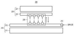
도 2는 일실시예에 따른 이종 칩이 3D 접합 구조로 형성되는 동일 반도체 패키지(200)를 설명하는 도면이다.FIG. 2 is a drawing illustrating an identical semiconductor package (200) in which heterogeneous chips are formed in a 3D bonding structure according to one embodiment.
일실시예에 따른 동일 반도체 패키지(200)는 하측 유닛(210)과 상측 유닛(220)이 서로 접합된 형태로 구현될 수 있다.According to one embodiment, the same semiconductor package (200) can be implemented in a form in which the lower unit (210) and the upper unit (220) are joined to each other.
먼저, 하측 유닛(210)은 제1 칩(211)과 제1 칩(211) 상 회로가 구현된 측면 상에서 형성된 제1 재배선층(212, RDL, Redistribution Layer)을 포함한다.First, the lower unit (210) includes a first chip (211) and a first redistribution layer (RDL, Redistribution Layer) (212) formed on the side where the circuit on the first chip (211) is implemented.
또한, 상측 유닛(220)은 제2 칩(221)과 제1 칩(221) 상 회로가 구현된 측면 상에서 형성된 제2 재배선층(222, RDL, Redistribution Layer)을 포함한다.Additionally, the upper unit (220) includes a second redistribution layer (RDL, Redistribution Layer) (222) formed on the side where the circuit of the second chip (221) and the first chip (221) are implemented.
일례로, 이종의 칩은 메모리칩과 ASIC(application specific integrated circuit)칩일 수 있다.For example, heterogeneous chips may be memory chips and application specific integrated circuit (ASIC) chips.
또한, 평면상 이종의 칩 중에서 어느 하나의 칩 면적이 더 크게 구현될 수 있다.Additionally, among the heterogeneous chips on a plane, one chip area can be implemented to be larger.
만약, ASIC(application specific integrated circuit)의 면적이 더 크게 구현되고, 메모리칩이 ASIC칩 보다 상대적으로 작게 구현되는 반도체 패키지라고 하면, 도 2에서 211이 ASIC칩이고, 212가 ASIC의 재배선층일 수 있다. 또한, 도면부호 221은 메모리칩이고, 222가 메모리칩의 재배선층일 수 있다.If the semiconductor package is implemented with a larger area of an ASIC (application specific integrated circuit) and a memory chip implemented relatively smaller than the ASIC chip, then 211 in FIG. 2 may be an ASIC chip and 212 may be a redistribution layer of the ASIC. In addition, drawing
또한, 다른 예로 메모리칩의 면적이 더 크게 구현되고, ASIC칩이 메모리칩 보다 상대적으로 작게 구현되는 반도체 패키지라고 하면, 도 2에서 211이 메모리칩이고, 212가 메모리칩의 재배선층일 수 있다.In addition, as another example, if a semiconductor package is implemented with a larger area of a memory chip and an ASIC chip is implemented relatively smaller than the memory chip, 211 in FIG. 2 may be a memory chip and 212 may be a redistribution layer of the memory chip.
도면부호 230은 제1 재배선층(212)과 제2 재배선층(222)을 전기적으로 연결시켜, 제1 칩(211)과 제2 칩(221)간 신호 송수신을 가능하게 하는 이종 칩간 연결채널(230)에 해당한다.Drawing
즉, 제1 재배선층과 상기 제2 재배선층이 마주보는(Face-to-Face) 구조에서, 제1 재배선층과 제2 재배선층을 통해 제1 칩과 제2 칩 간 전기적 연결을 제공하는 이종 칩간 연결채널(230)에 해당한다.That is, in a structure where the first redistribution layer and the second redistribution layer face each other (face-to-face), it corresponds to a heterogeneous chip connection channel (230) that provides electrical connection between the first chip and the second chip through the first redistribution layer and the second redistribution layer.
한편, 도면부호 213은 외부신호를 수신하기 위한 PAD에 해당한다.Meanwhile, drawing
메모리칩의 면적이 큰 경우와 ASIC칩의 면적이 큰 경우의 각각에 대해 외부신호 및 내부신호의 흐름이 달라진다.The flow of external and internal signals differs depending on whether the area of the memory chip is large or the area of the ASIC chip is large.
이하, 도 3 및 도 4에서는 메모리칩의 면적이 크고 ASIC칩의 면적이 작은 경우, 메모리칩의 면적이 작고 ASIC칩의 면적이 큰 경우를 구분하여 외부신호 및 내부신호의 흐름을 설명한다.Below, in FIGS. 3 and 4, the flow of external and internal signals is explained by distinguishing between the case where the area of the memory chip is large and the area of the ASIC chip is small, and the case where the area of the memory chip is small and the area of the ASIC chip is large.
도 3은 ASIC칩(311)이 메모리칩(321)보다 큰 경우의 외부 및 내부신호 흐름도를 도시하는 도면이다.Figure 3 is a diagram showing external and internal signal flow diagrams when the ASIC chip (311) is larger than the memory chip (321).
ASIC칩(311)이 메모리칩(321)보다 큰 경우, 외부 연결을 위한 PAD(313)는 ASIC칩(311) 상 재배선층(312)에 위치하고 메모리칩(321)에 필요한 전원전압을 제외하고 ASIC칩(311) 상 재배선층(312)으로만 연결된다.When the ASIC chip (311) is larger than the memory chip (321), the PAD (313) for external connection is located on the redistribution layer (312) on the ASIC chip (311) and is connected only to the redistribution layer (312) on the ASIC chip (311) except for the power voltage required for the memory chip (321).
본 발명의 배경으로 기 서술한 동일 패키지 내 이종 칩 간, 특히 크기가 다른 메모리칩과 ASIC칩을 3D 적층함에 있어 두 칩간 연결은 회로가 구현된 면을 기준으로 상호 마주보는 구조로 구현함 (F2F: Face-to-Face)을 주요 특징으로 함으로서 외부 연결을 위한 PAD구현 중에 TSV 공정이 필요 없게 된다.As described above as the background of the present invention, when 3D stacking different chips within the same package, particularly memory chips and ASIC chips of different sizes, the connection between the two chips is implemented in a structure where the circuits are implemented facing each other based on the surface (F2F: Face-to-Face), which is a key feature, so that the TSV process is not required during the implementation of the PAD for external connection.
도 3의 실시예에 따르면, 제1 칩(메모리칩)과 제2 칩(ASIC칩)의 크기에 따른 신호 전달 체계를 살펴볼 수 있다.According to the embodiment of Fig. 3, a signal transmission system according to the size of the first chip (memory chip) and the second chip (ASIC chip) can be examined.
도 3의 실시예는 평면상 제2 칩(ASIC칩)의 면적이 제1 칩(메모리칩)의 면적 보다 큰 경우에 해당한다.The embodiment of Fig. 3 corresponds to a case where the area of the second chip (ASIC chip) on the plane is larger than the area of the first chip (memory chip).
이때, 제2 칩(ASIC칩) 상에 형성되어 있는 제2 재배선층을 통해 제2 칩(ASIC칩)에서 외부신호를 수신하고, 수신된 외부신호를 기반으로, 제2 칩(ASIC칩)의 용도에 부합되도록 설계된 선정된 로직에 따라 내부신호를 생성할 수 있다.At this time, an external signal can be received from the second chip (ASIC chip) through the second redistribution layer formed on the second chip (ASIC chip), and an internal signal can be generated based on the received external signal according to a selected logic designed to match the purpose of the second chip (ASIC chip).
또한, 생성된 내부신호를 이종 칩간 연결채널을 통해 제2 칩에서 제1 칩으로 전달할 수 있다.Additionally, the generated internal signal can be transmitted from the second chip to the first chip through a heterogeneous chip connection channel.
도 4는 메모리칩(411)이 ASIC칩(421)보다 큰 경우의 외부 및 내부신호 흐름도를 도시하는 도면이다.Figure 4 is a diagram showing external and internal signal flow diagrams when the memory chip (411) is larger than the ASIC chip (421).
메모리칩(411)이 ASIC칩(421)보다 큰 경우, 외부 연결 PAD(413)는 메모리칩 상 재배선층(412)에만 위치하고 메모리칩(411)에 필요한 전원전압을 제외하고 ASIC칩(421)으로만 3D 적층기술을 사용하여 연결될 수 있다.When the memory chip (411) is larger than the ASIC chip (421), the external connection PAD (413) is located only on the redistribution layer (412) on the memory chip and can be connected only to the ASIC chip (421) using 3D stacking technology, excluding the power voltage required for the memory chip (411).
만약 메모리칩(411)이 ASIC칩(421)보다 큰 경우, 외부 연결 패드(413)는 메모리칩(411)의 재배선층(412)을 통해 메모리칩에는 연결되지 않고 이종 칩간 3D 연결 통로(TSV 또는 Hybrid bonding)로 ASIC칩으로 연결되어 효율적 신호 구성이 가능하게 된다.If the memory chip (411) is larger than the ASIC chip (421), the external connection pad (413) is not connected to the memory chip through the redistribution layer (412) of the memory chip (411), but is connected to the ASIC chip through a 3D connection passage (TSV or hybrid bonding) between heterogeneous chips, thereby enabling efficient signal configuration.
상기 두가지 이종 칩의 크기에 따른 적층 방법 및 외부신호 연결 방법에 있어 메모리칩에는 파워신호를 제외하고 모든 신호는 ASIC칩으로 직접 연결되는 구조를 나타낸다.In the stacking method and external signal connection method according to the size of the two different chips mentioned above, the memory chip shows a structure in which all signals except the power signal are directly connected to the ASIC chip.
즉, ASIC칩이 적층되는 메모리칩을 전용으로 활용할 수 있는 특징을 가지게 되어 AI응용 등의 대용량 메모리 접근이 많은 미래 반도체칩의 효율적 구현이 가능하다.In other words, it has the characteristic of being able to exclusively utilize memory chips on which ASIC chips are stacked, enabling efficient implementation of future semiconductor chips that require a lot of large-capacity memory access, such as AI applications.
도 4의 실시예에 따르면, 제1 칩(메모리칩)과 제2 칩(ASIC칩)의 크기에 따른 신호 전달 체계를 살펴볼 수 있다.According to the embodiment of Fig. 4, a signal transmission system according to the size of the first chip (memory chip) and the second chip (ASIC chip) can be examined.
도 4는 평면상 제1 칩(메모리칩)의 면적이 제2 칩(ASIC칩) 보다 큰 경우, 제1 칩(메모리칩)의 제1 재배선층에서 외부신호를 수신하고, 수신된 외부신호를 이종 칩간 연결채널을 통해 제2 칩(ASIC칩)으로 전달할 수 있다.FIG. 4 shows a case where the area of a first chip (memory chip) on a plane is larger than that of a second chip (ASIC chip), an external signal can be received from the first rewiring layer of the first chip (memory chip), and the received external signal can be transmitted to the second chip (ASIC chip) through a heterogeneous chip connection channel.
또한, 제1 재배선층으로부터 전달된 외부신호에 대해 제2 칩(ASIC칩)의 선정된 로직에 따라 내부신호를 생성하고, 생성된 내부신호를 제2 칩(ASIC칩)으로부터 이종 칩간 연결채널을 통해 제1 칩(메모리칩)으로 전달할 수 있다.In addition, an internal signal can be generated according to the selected logic of the second chip (ASIC chip) for an external signal transmitted from the first rewiring layer, and the generated internal signal can be transmitted from the second chip (ASIC chip) to the first chip (memory chip) through a heterogeneous chip connection channel.
도 5는 이종 칩간 상호 다른 전원 전압을 가진 경우 신호 크기를 맞춰주는 Level-shift가 ASIC칩에 있는 실시예를 도시하는 도면이다.FIG. 5 is a diagram illustrating an embodiment in which a level shifter for adjusting signal sizes when different power supply voltages are used between heterogeneous chips is included in an ASIC chip.
ASIC칩과 메모리칩간 상호 신호 연결 로직 블록은 동일 전압으로 동작이 필요하다.The logic blocks that interconnect signals between ASIC chips and memory chips must operate at the same voltage.
따라서, 도면부호 500과 같이 이종 전원 전압을 사용하는 ASIC칩과 메모리칩의 상호 신호 연결 로직 블록(510)은 별도의 전원 전압을 가짐을 특징으로 할 수 있으며 전원 전압 간의 차이를 극복하는 Level-shift 회로가 추가될 수 있다.Accordingly, the logic block (510) for interconnecting signals between an ASIC chip and a memory chip using different power supply voltages, such as the
신호 연결 로직 블록은 전원전압이 이종 칩의 전원전압 중 어느 한쪽의 전원과 동일 할 수 있다.The signal connection logic block can have its power supply voltage identical to that of either of the heterogeneous chips.
ASIC칩과 3D 적층기술을 사용하여 연결되는 메모리칩의 활성화는 ASIC칩의 내부 동작에 의해서만 가능하며 다른 Bank-group에 대해 읽기 및 쓰기 동작을 동시에 수행할 수 있다.Activation of memory chips connected using ASIC chips and 3D stacking technology is possible only through the internal operation of the ASIC chip, and read and write operations for different bank groups can be performed simultaneously.
메모리칩은 다수의 재배선층을 사용하여 ASIC칩과 연결될 수 있다.Memory chips can be connected to ASIC chips using multiple redistribution layers.
또한, 메모리칩은 동일한 설계를 사용하고 다른 RDL mask-set의 조합에 의해 구현될 수 있다. 동일한 메모리칩 설계와 조합되는 RDL mask-set에 의해 다른 configuration의 메모리칩이 될 수 있고, 재배선층의 mask-set으로 구현되는 다른 configuration의 메모리칩은 특히, I/O width (# of data bits)가 변경되어 다양한 응용에 효과적으로 대응될 수 있다.In addition, the memory chip can be implemented by using the same design and combining different RDL mask sets. The memory chip can have a different configuration by combining the same memory chip design and the RDL mask set, and the memory chip of a different configuration implemented by the mask set of the redistribution layer can effectively respond to various applications, especially by changing the I/O width (# of data bits).
도 6은 일실시예에 따른 이종 칩이 3D 접합 구조로 형성되는 동일 반도체 패키지의 동작 방법을 설명하는 도면이다.FIG. 6 is a drawing explaining an operation method of an identical semiconductor package in which heterogeneous chips are formed in a 3D bonding structure according to one embodiment.
일실시예에 따른 이종 칩이 3D 접합 구조로 형성되는 동일 반도체 패키지의 동작 방법은 회로가 구현된 측면을 기준으로 상호 마주보는(Face-to-Face) 이종의 제1 칩 및 제2 칩이 3D 접합 구조로 형성되는 동일 반도체 패키지의 동작 방법에 관한 것으로서, 평면상 ASIC칩의 면적이 메모리칩의 면적 보다 큰 경우를 나타낸다.An operating method of an identical semiconductor package in which heterogeneous chips are formed in a 3D bonding structure according to an embodiment of the present invention relates to an operating method of an identical semiconductor package in which heterogeneous first chips and second chips are formed in a 3D bonding structure, which face each other (face-to-face) based on a side on which a circuit is implemented, and represents a case in which an area of an ASIC chip in a plane is larger than an area of a memory chip.
일실시예에 따른 이종 칩이 3D 접합 구조로 형성되는 동일 반도체 패키지의 동작 방법은 제2 칩 상에 형성된 제2 재배선층(RDL, Redistribution Layer)을 통해 제2 칩에서 외부신호를 수신할 수 있다(단계 601).According to an embodiment, a method for operating an identical semiconductor package in which heterogeneous chips are formed in a 3D bonding structure can receive an external signal from a second chip through a second redistribution layer (RDL) formed on a second chip (step 601).
또한, 일실시예에 따른 이종 칩이 3D 접합 구조로 형성되는 동일 반도체 패키지의 동작 방법은 제2 칩에서 상기 수신된 외부신호를 기반으로, 선정된 로직에 따라 내부신호를 생성할 수 있다(단계 602).In addition, the method of operating the same semiconductor package in which the heterogeneous chips according to one embodiment are formed in a 3D bonding structure can generate an internal signal according to a selected logic based on the external signal received from the second chip (step 602).
일실시예에 따른 이종 칩이 3D 접합 구조로 형성되는 동일 반도체 패키지의 동작 방법은 생성된 내부신호를 이종 칩간 연결채널을 통해 제2 칩에서 제1 칩으로 전달할 수 있다(단계 603).According to an embodiment of the present invention, a method for operating an identical semiconductor package in which heterogeneous chips are formed in a 3D bonding structure can transmit a generated internal signal from a second chip to a first chip through a heterogeneous chip connection channel (step 603).
일실시예에 따른 이종 칩이 3D 접합 구조로 형성되는 동일 반도체 패키지의 동작 방법은 제1 칩에서 상기 내부신호를 수신하고, 상기 수신된 내부신호에 따라 동작할 수 있다(단계 604).According to an embodiment, a method for operating an identical semiconductor package in which heterogeneous chips are formed in a 3D bonding structure may receive the internal signal from the first chip and operate according to the received internal signal (step 604).
도 7은 다른 일실시예에 따른 이종 칩이 3D 접합 구조로 형성되는 동일 반도체 패키지의 동작 방법을 설명하는 도면이다.FIG. 7 is a drawing explaining an operation method of an identical semiconductor package in which heterogeneous chips are formed in a 3D bonding structure according to another embodiment.
다른 일실시예에 따른 이종 칩이 3D 접합 구조로 형성되는 동일 반도체 패키지의 동작 방법은 평면상 메모리칩의 면적이 ASIC칩의 면적 보다 큰 경우를 나타낸다.According to another embodiment, a method of operating an identical semiconductor package in which heterogeneous chips are formed in a 3D bonding structure is described, wherein the area of a memory chip in a plane is larger than the area of an ASIC chip.
일실시예에 따른 이종 칩이 3D 접합 구조로 형성되는 동일 반도체 패키지의 동작 방법은 제1 칩 상에 형성된 제1 재배선층에서 외부신호를 수신할 수 있다.According to one embodiment, a method for operating an identical semiconductor package in which heterogeneous chips are formed in a 3D bonding structure can receive an external signal from a first redistribution layer formed on a first chip.
다음으로, 일실시예에 따른 이종 칩이 3D 접합 구조로 형성되는 동일 반도체 패키지의 동작 방법은 수신된 외부신호를 상기 이종 칩간 연결채널을 통해 상기 제2 칩으로 전달할 수 있다.Next, the method of operating the same semiconductor package in which heterogeneous chips are formed in a 3D bonding structure according to one embodiment can transmit a received external signal to the second chip through the heterogeneous chip connection channel.
또한, 일실시예에 따른 이종 칩이 3D 접합 구조로 형성되는 동일 반도체 패키지의 동작 방법은 제2 칩에서 상기 전달된 외부신호에 대해 상기 제2 칩의 선정된 로직에 따라 내부신호를 생성할 수 있다.In addition, the method of operating the same semiconductor package in which the heterogeneous chips according to one embodiment are formed in a 3D bonding structure can generate an internal signal according to the selected logic of the second chip in response to the external signal transmitted from the second chip.
일실시예에 따른 이종 칩이 3D 접합 구조로 형성되는 동일 반도체 패키지의 동작 방법은 제2 칩에서 상기 생성된 내부신호를 상기 이종 칩간 연결채널을 통해 상기 제1 칩으로 전달할 수 있다.According to one embodiment, a method for operating an identical semiconductor package in which heterogeneous chips are formed in a 3D bonding structure can transmit an internal signal generated in a second chip to the first chip through the heterogeneous chip connection channel.
다음으로, 일실시예에 따른 이종 칩이 3D 접합 구조로 형성되는 동일 반도체 패키지의 동작 방법은 제1 칩에서 내부신호를 수신하고, 수신된 내부신호에 따라 동작할 수 있다.Next, a method of operating an identical semiconductor package in which heterogeneous chips according to one embodiment are formed in a 3D bonding structure can receive an internal signal from a first chip and operate according to the received internal signal.
결국, 본 발명을 이용하면, 동일 패키지 내 이종 칩 간, 특히 다른 크기를 갖는 메모리칩과 ASIC간의 적층 순서 및 외부신호와의 연결 방법 및 칩 간 내부신호의 물리적 연결 방법을 제공할 수 있다.Ultimately, by utilizing the present invention, it is possible to provide a stacking order between different chips within the same package, particularly between memory chips and ASICs having different sizes, a connection method with external signals, and a physical connection method of internal signals between chips.
또한, 소비전력의 비효율 요소 제거 및 효과적인 신호 연결 방법을 제시할 수 있고, NDP(Near Data Processing)이 필요한 ASIC에 대용량 메모리의 적용이 용이함과 더불어 다른 공정을 사용하는 메모리와 ASIC간 원활한 연결 기술을 위해 응용별 규격화된 물리적 연결 방법을 제공할 수 있다.In addition, it is possible to provide a method for eliminating inefficient elements of power consumption and an effective signal connection method, and it is possible to provide a physical connection method standardized for each application for easy application of large-capacity memory to ASICs requiring NDP (Near Data Processing) and for smooth connection technology between memories and ASICs using different processes.
뿐만 아니라, ASIC칩 및 메모리칩의 3D 연결을 위한 각각 별도의 layer (RDL)를 가지게 되면, RDL을 갖는 ASIC칩은 RDL만의 변경으로 효율적으로 다른 configuration을 갖도록 구현할 수 있고, RDL을 갖는 메모리칩을 이용하여 RDL만의 변경으로 효율적으로 다른 configuration을 갖도록 구현할 수 있다.In addition, if ASIC chips and memory chips each have a separate layer (RDL) for 3D connection, an ASIC chip having an RDL can be implemented to have a different configuration efficiently by changing only the RDL, and a memory chip having an RDL can be implemented to have a different configuration efficiently by changing only the RDL.
또한, 본 발명을 이용하면, ASIC칩 및 메모리칩의 3D 연결과, RDL을 갖는 메모리칩을 이용한 다양한 조합으로 빠른 생산을 가능하게 할 수 있고, 두가지 이종 Die의 접합에 대해 회로가 구현된 측면을 기준으로 상호 바라다 보게 구현하고 (Face-to-Face) 면적이 큰 칩을 기준으로 PAD를 구현함에 따라 TSV(Through Silicon Via)를 생략할 수 있다.In addition, by utilizing the present invention, rapid production can be enabled with 3D connection of ASIC chips and memory chips, and various combinations using memory chips having RDLs, and, for bonding of two different dies, the circuits are implemented so that they face each other (Face-to-Face) and the PAD is implemented based on a chip with a large area, thereby allowing TSV (Through Silicon Via) to be omitted.
이를 통해, RDL이 없는 메모리칩을 표준화하여 미래 메모리 파운드리 모델을 제공할 수 있다.This will allow standardization of RDL-less memory chips, providing a future memory foundry model.
이상에서 설명된 장치는 하드웨어 구성요소, 소프트웨어 구성요소, 및/또는 하드웨어 구성요소 및 소프트웨어 구성요소의 조합으로 구현될 수 있다. 예를 들어, 실시예들에서 설명된 장치 및 구성요소는, 예를 들어, 프로세서, 콘트롤러, ALU(arithmetic logic unit), 디지털 신호 프로세서(digital signal processor), 마이크로컴퓨터, FPA(field programmable array), PLU(programmable logic unit), 마이크로프로세서, 또는 명령(instruction)을 실행하고 응답할 수 있는 다른 어떠한 장치와 같이, 하나 이상의 범용 컴퓨터 또는 특수 목적 컴퓨터를 이용하여 구현될 수 있다. 처리 장치는 운영 체제(OS) 및 상기 운영 체제 상에서 수행되는 하나 이상의 소프트웨어 애플리케이션을 수행할 수 있다. 또한, 처리 장치는 소프트웨어의 실행에 응답하여, 데이터를 접근, 저장, 조작, 처리 및 생성할 수도 있다. 이해의 편의를 위하여, 처리 장치는 하나가 사용되는 것으로 설명된 경우도 있지만, 해당 기술분야에서 통상의 지식을 가진 자는, 처리 장치가 복수 개의 처리 요소(processing element) 및/또는 복수 유형의 처리 요소를 포함할 수 있음을 알 수 있다. 예를 들어, 처리 장치는 복수 개의 프로세서 또는 하나의 프로세서 및 하나의 콘트롤러를 포함할 수 있다. 또한, 병렬 프로세서(parallel processor)와 같은, 다른 처리 구성(processing configuration)도 가능하다.The devices described above may be implemented as hardware components, software components, and/or a combination of hardware components and software components. For example, the devices and components described in the embodiments may be implemented using one or more general-purpose computers or special-purpose computers, such as, for example, a processor, a controller, an arithmetic logic unit (ALU), a digital signal processor, a microcomputer, a field programmable array (FPA), a programmable logic unit (PLU), a microprocessor, or any other device capable of executing instructions and responding to them. The processing device may execute an operating system (OS) and one or more software applications running on the operating system. In addition, the processing device may access, store, manipulate, process, and generate data in response to the execution of the software. For ease of understanding, the processing device is sometimes described as being used alone, but those skilled in the art will appreciate that the processing device may include multiple processing elements and/or multiple types of processing elements. For example, the processing device may include multiple processors, or a processor and a controller. Other processing configurations, such as parallel processors, are also possible.
소프트웨어는 컴퓨터 프로그램(computer program), 코드(code), 명령(instruction), 또는 이들 중 하나 이상의 조합을 포함할 수 있으며, 원하는 대로 동작하도록 처리 장치를 구성하거나 독립적으로 또는 결합적으로(collectively) 처리 장치를 명령할 수 있다. 소프트웨어 및/또는 데이터는, 처리 장치에 의하여 해석되거나 처리 장치에 명령 또는 데이터를 제공하기 위하여, 어떤 유형의 기계, 구성요소(component), 물리적 장치, 가상 장치(virtual equipment), 컴퓨터 저장 매체 또는 장치, 또는 전송되는 신호 파(signal wave)에 영구적으로, 또는 일시적으로 구체화(embody)될 수 있다. 소프트웨어는 네트워크로 연결된 컴퓨터 시스템 상에 분산되어서, 분산된 방법으로 저장되거나 실행될 수도 있다. 소프트웨어 및 데이터는 하나 이상의 컴퓨터 판독 가능 기록 매체에 저장될 수 있다.The software may include a computer program, code, instructions, or a combination of one or more of these, which may configure a processing device to perform a desired operation or may independently or collectively command the processing device. The software and/or data may be permanently or temporarily embodied in any type of machine, component, physical device, virtual equipment, computer storage medium or device, or transmitted signal waves, for interpretation by the processing device or for providing instructions or data to the processing device. The software may also be distributed over network-connected computer systems, and stored or executed in a distributed manner. The software and data may be stored on one or more computer-readable recording media.
실시예에 따른 방법은 다양한 컴퓨터 수단을 통하여 수행될 수 있는 프로그램 명령 형태로 구현되어 컴퓨터 판독 가능 매체에 기록될 수 있다. 상기 컴퓨터 판독 가능 매체는 프로그램 명령, 데이터 파일, 데이터 구조 등을 단독으로 또는 조합하여 포함할 수 있다. 상기 매체에 기록되는 프로그램 명령은 실시예를 위하여 특별히 설계되고 구성된 것들이거나 컴퓨터 소프트웨어 당업자에게 공지되어 사용 가능한 것일 수도 있다. 컴퓨터 판독 가능 기록 매체의 예에는 하드 디스크, 플로피 디스크 및 자기 테이프와 같은 자기 매체(magnetic media), CD-ROM, DVD와 같은 광기록 매체(optical media), 플롭티컬 디스크(floptical disk)와 같은 자기-광 매체(magneto-optical media), 및 롬(ROM), 램(RAM), 플래시 메모리 등과 같은 프로그램 명령을 저장하고 수행하도록 특별히 구성된 하드웨어 장치가 포함된다. 프로그램 명령의 예에는 컴파일러에 의해 만들어지는 것과 같은 기계어 코드뿐만 아니라 인터프리터 등을 사용해서 컴퓨터에 의해서 실행될 수 있는 고급 언어 코드를 포함한다. 상기된 하드웨어 장치는 실시예의 동작을 수행하기 위해 하나 이상의 소프트웨어 모듈로서 작동하도록 구성될 수 있으며, 그 역도 마찬가지이다.The method according to the embodiment may be implemented in the form of program commands that can be executed through various computer means and recorded on a computer-readable medium. The computer-readable medium may include program commands, data files, data structures, etc., alone or in combination. The program commands recorded on the medium may be those specially designed and configured for the embodiment or may be those known to and available to those skilled in the art of computer software. Examples of the computer-readable recording medium include magnetic media such as hard disks, floppy disks, and magnetic tapes, optical media such as CD-ROMs and DVDs, magneto-optical media such as floptical disks, and hardware devices specially configured to store and execute program commands such as ROMs, RAMs, flash memories, etc. Examples of the program commands include not only machine language codes generated by a compiler but also high-level language codes that can be executed by a computer using an interpreter, etc. The hardware devices described above may be configured to operate as one or more software modules to perform the operations of the embodiment, and vice versa.
이상과 같이 실시예들이 비록 한정된 도면에 의해 설명되었으나, 해당 기술분야에서 통상의 지식을 가진 자라측면 상이기의 기재로부터 다양한 수정 및 변형이 가능하다. 예를 들어, 설명된 기술들이 설명된 방법과 다른 순서로 수행되거나, 및/또는 설명된 시스템, 구조, 장치, 회로 등의 구성요소들이 설명된 방법과 다른 형태로 결합 또는 조합되거나, 다른 구성요소 또는 균등물에 의하여 대치되거나 치환되더라도 적절한 결과가 달성될 수 있다.Although the embodiments have been described with reference to limited drawings, those skilled in the art will appreciate that various modifications and variations may be made based on the description of the invention. For example, the described techniques may be performed in a different order than described, and/or the components of the described systems, structures, devices, circuits, etc. may be combined or combined in a different form than described, or may be replaced or substituted by other components or equivalents, and still achieve appropriate results.
그러므로, 다른 구현들, 다른 실시예들 및 특허청구범위와 균등한 것들도 후술하는 특허청구범위의 범위에 속한다.Therefore, other implementations, other embodiments, and equivalents to the claims are also included in the scope of the claims described below.
Claims (8)
Translated fromKorean회로가 구현된 측면 상에서 제1 재배선층(RDL, Redistribution Layer)이 형성된 제1 칩;
상기 제1 칩과는 이종의 칩으로서, 회로가 구현된 측면 상에서 제2 재배선층(RDL, Redistribution Layer)이 형성된 제2 칩; 및
상기 제1 재배선층과 상기 제2 재배선층이 마주보는(Face-to-Face) 구조에서, 상기 제1 재배선층과 상기 제2 재배선층을 통해 상기 제1 칩과 상기 제2 칩 간 전기적 연결을 제공하는 이종 칩간 연결채널
을 포함하고,
평면상 상기 제1 칩의 면적이 상기 제2 칩 보다 큰 경우,
상기 제1 칩의 상기 제1 재배선층에서 외부신호를 수신하고, 상기 수신된 외부신호를 상기 이종 칩간 연결채널을 통해 상기 제2 칩으로 전달하며, 상기 제1 재배선층으로부터 전달된 외부신호에 대해 상기 제2 칩의 선정된 로직에 따라 내부신호를 생성하고, 상기 생성된 내부신호를 상기 제2 칩으로부터 상기 이종 칩간 연결채널을 통해 상기 제1 칩으로 전달하는 것을 특징으로 하는 이종 칩이 3D 접합 구조로 형성되는 동일 반도체 패키지.It relates to an identical semiconductor package in which different chips are formed in a 3D bonding structure (Face-to-Face) based on the side where the circuit is implemented.
A first chip having a first redistribution layer (RDL) formed on the side where the circuit is implemented;
A second chip, which is a different chip from the first chip, and has a second redistribution layer (RDL) formed on the side where the circuit is implemented; and
In a structure where the first redistribution layer and the second redistribution layer face each other (Face-to-Face), a heterogeneous chip-to-chip connection channel that provides electrical connection between the first chip and the second chip through the first redistribution layer and the second redistribution layer
Including,
If the area of the first chip on the plane is larger than that of the second chip,
An identical semiconductor package in which heterogeneous chips are formed in a 3D bonding structure, characterized in that an external signal is received from the first rewiring layer of the first chip, the received external signal is transmitted to the second chip through the heterogeneous chip connection channel, an internal signal is generated according to the selected logic of the second chip in response to the external signal transmitted from the first rewiring layer, and the generated internal signal is transmitted from the second chip to the first chip through the heterogeneous chip connection channel.
상기 제1 칩은 메모리칩이고, 상기 제2 칩은 ASIC(application specific integrated circuit) 칩인 것을 특징으로 하는 이종 칩이 3D 접합 구조로 형성되는 동일 반도체 패키지.In the first paragraph,
An identical semiconductor package in which heterogeneous chips are formed in a 3D bonding structure, wherein the first chip is a memory chip and the second chip is an ASIC (application specific integrated circuit) chip.
상기 제1 칩과 제2 칩의 신호 연결을 위한 회로에는 동일 전원 전압을 사용하고,
상기 제1 칩 또는 상기 제2 칩 중에서 평면상 면적이 큰 칩의 재배선층을 통해 외부신호가 전달되는 것을 특징으로 하는 이종 칩이 3D 접합 구조로 형성되는 동일 반도체 패키지.In the first paragraph,
The circuit for signal connection between the first chip and the second chip uses the same power supply voltage,
An identical semiconductor package in which heterogeneous chips are formed in a 3D bonding structure, characterized in that an external signal is transmitted through a redistribution layer of a chip having a larger planar area among the first chip or the second chip.
평면상 상기 제1 칩의 면적이 상기 제2 칩 보다 큰 경우,
상기 제1 칩 상에 형성된 제1 재배선층에서 외부신호를 수신하는 단계;
상기 수신된 외부신호를 상기 이종 칩간 연결채널을 통해 상기 제2 칩으로 전달하는 단계;
상기 제2 칩에서 상기 전달된 외부신호에 대해 상기 제2 칩의 선정된 로직에 따라 내부신호를 생성하는 단계;
상기 제2 칩에서 상기 생성된 내부신호를 상기 이종 칩간 연결채널을 통해 상기 제1 칩으로 전달하는 단계; 및
상기 제1 칩에서 상기 내부신호를 수신하고, 상기 수신된 내부신호에 따라 동작하는 단계
를 포함하는 이종 칩이 3D 접합 구조로 형성되는 동일 반도체 패키지의 동작 방법.A method of operating an identical semiconductor package in which a first chip and a second chip of different types are formed in a 3D bonding structure, with the first chip and the second chip facing each other (Face-to-Face) based on the side where the circuit is implemented, is disclosed.
If the area of the first chip on the plane is larger than that of the second chip,
A step of receiving an external signal from a first rewiring layer formed on the first chip;
A step of transmitting the received external signal to the second chip through the heterogeneous chip connection channel;
A step of generating an internal signal according to the selected logic of the second chip in response to the external signal transmitted from the second chip;
A step of transmitting the internal signal generated in the second chip to the first chip through the heterogeneous chip connection channel; and
A step of receiving the internal signal from the first chip and operating according to the received internal signal
A method for operating an identical semiconductor package in which heterogeneous chips including a 3D bonding structure are formed.
상기 제1 칩은 메모리칩이고, 상기 제2 칩은 ASIC(application specific integrated circuit) 칩인 것을 특징으로 하는 이종 칩이 3D 접합 구조로 형성되는 동일 반도체 반도체 패키지의 동작 방법.In any one of the 7 clauses,
An operating method of an identical semiconductor package in which heterogeneous chips are formed in a 3D bonding structure, wherein the first chip is a memory chip and the second chip is an ASIC (application specific integrated circuit) chip.
Priority Applications (1)
| Application Number | Priority Date | Filing Date | Title |
|---|---|---|---|
| KR1020230135119AKR102826267B1 (en) | 2023-10-11 | 2023-10-11 | Semiconductor package with heterogeneous chips formed in a 3d stacking structure and the operation method of the package |
Applications Claiming Priority (1)
| Application Number | Priority Date | Filing Date | Title |
|---|---|---|---|
| KR1020230135119AKR102826267B1 (en) | 2023-10-11 | 2023-10-11 | Semiconductor package with heterogeneous chips formed in a 3d stacking structure and the operation method of the package |
Publications (2)
| Publication Number | Publication Date |
|---|---|
| KR20250052053A KR20250052053A (en) | 2025-04-18 |
| KR102826267B1true KR102826267B1 (en) | 2025-06-26 |
Family
ID=95579286
Family Applications (1)
| Application Number | Title | Priority Date | Filing Date |
|---|---|---|---|
| KR1020230135119AActiveKR102826267B1 (en) | 2023-10-11 | 2023-10-11 | Semiconductor package with heterogeneous chips formed in a 3d stacking structure and the operation method of the package |
Country Status (1)
| Country | Link |
|---|---|
| KR (1) | KR102826267B1 (en) |
Citations (2)
| Publication number | Priority date | Publication date | Assignee | Title |
|---|---|---|---|---|
| JP2006032379A (en)* | 2004-07-12 | 2006-02-02 | Akita Denshi Systems:Kk | Laminate semiconductor device and its manufacturing method |
| JP2013131283A (en) | 2011-12-22 | 2013-07-04 | Elpida Memory Inc | Semiconductor device |
Family Cites Families (5)
| Publication number | Priority date | Publication date | Assignee | Title |
|---|---|---|---|---|
| KR101683814B1 (en)* | 2010-07-26 | 2016-12-08 | 삼성전자주식회사 | Semiconductor apparatus having through vias |
| JP2012255704A (en)* | 2011-06-08 | 2012-12-27 | Elpida Memory Inc | Semiconductor device |
| KR102617088B1 (en) | 2019-09-18 | 2023-12-26 | 삼성전자주식회사 | Semiconductor package |
| KR102724661B1 (en) | 2020-06-03 | 2024-10-31 | 삼성전자주식회사 | semiconductor package for improving a package reliability |
| KR20230010397A (en) | 2021-07-12 | 2023-01-19 | 에스케이하이닉스 주식회사 | Semiconductor Packages Including Different Type Semiconductor chips Having Exposed Top Surfaces and Method of Manufacturing the Semiconductor Packages |
- 2023
- 2023-10-11KRKR1020230135119Apatent/KR102826267B1/enactiveActive
Patent Citations (2)
| Publication number | Priority date | Publication date | Assignee | Title |
|---|---|---|---|---|
| JP2006032379A (en)* | 2004-07-12 | 2006-02-02 | Akita Denshi Systems:Kk | Laminate semiconductor device and its manufacturing method |
| JP2013131283A (en) | 2011-12-22 | 2013-07-04 | Elpida Memory Inc | Semiconductor device |
Also Published As
| Publication number | Publication date |
|---|---|
| KR20250052053A (en) | 2025-04-18 |
Similar Documents
| Publication | Publication Date | Title |
|---|---|---|
| US20230138386A1 (en) | Bridge hub tiling architecture | |
| TWI748291B (en) | Integrated circuit device, interconnection device die and fabrication method for system on integrated chip | |
| US9361254B2 (en) | Memory device formed with a semiconductor interposer | |
| US20200098725A1 (en) | Semiconductor package or semiconductor package structure with dual-sided interposer and memory | |
| US8710676B2 (en) | Stacked structure and stacked method for three-dimensional chip | |
| US20200098724A1 (en) | Semiconductor package or structure with dual-sided interposers and memory | |
| TWI681525B (en) | Flexible memory system with a controller and a stack of memory | |
| US9941253B1 (en) | Semiconductor packages including interconnectors and methods of fabricating the same | |
| US20230352412A1 (en) | Multiple die package using an embedded bridge connecting dies | |
| KR102367512B1 (en) | System on package | |
| JP2025114585A (en) | Multi-chip structure including a memory die stacked on a die with a programmable integrated circuit - Patent Application 20070122997 | |
| JP2016513872A (en) | Via use package on package | |
| US9466593B2 (en) | Stack semiconductor package | |
| US12386761B2 (en) | Memory and routing module for use in a computer system | |
| Su et al. | 3D-MiM (MUST-in-MUST) technology for advanced system integration | |
| US20150364454A1 (en) | Reconfigured wide i/o memory modules and package architectures using same | |
| CN114036086B (en) | Three-dimensional heterogeneous integration-based serial interface memory chip | |
| CN117457619B (en) | A semiconductor device based on high bandwidth interconnect technology | |
| KR102826267B1 (en) | Semiconductor package with heterogeneous chips formed in a 3d stacking structure and the operation method of the package | |
| KR20250141219A (en) | Multi-stack computing chip and memory architecture | |
| CN114203640B (en) | A method for interconnecting detachable bit-width DDR modules based on SiP stacking structure | |
| CN115203097A (en) | A HBM storage system compatible with traditional packaging | |
| KR20230120530A (en) | Computing device guaranteeing bandwidth per computational performance and electronic device including same | |
| US20250300111A1 (en) | High bandwidth memory multi-stack package | |
| US8947152B2 (en) | Multi-chip package |
Legal Events
| Date | Code | Title | Description |
|---|---|---|---|
| PA0109 | Patent application | St.27 status event code:A-0-1-A10-A12-nap-PA0109 | |
| PA0201 | Request for examination | St.27 status event code:A-1-2-D10-D11-exm-PA0201 | |
| D13-X000 | Search requested | St.27 status event code:A-1-2-D10-D13-srh-X000 | |
| D14-X000 | Search report completed | St.27 status event code:A-1-2-D10-D14-srh-X000 | |
| PE0902 | Notice of grounds for rejection | St.27 status event code:A-1-2-D10-D21-exm-PE0902 | |
| T11-X000 | Administrative time limit extension requested | St.27 status event code:U-3-3-T10-T11-oth-X000 | |
| E13-X000 | Pre-grant limitation requested | St.27 status event code:A-2-3-E10-E13-lim-X000 | |
| P11-X000 | Amendment of application requested | St.27 status event code:A-2-2-P10-P11-nap-X000 | |
| PG1501 | Laying open of application | St.27 status event code:A-1-1-Q10-Q12-nap-PG1501 | |
| E701 | Decision to grant or registration of patent right | ||
| PE0701 | Decision of registration | St.27 status event code:A-1-2-D10-D22-exm-PE0701 | |
| GRNT | Written decision to grant | ||
| PR0701 | Registration of establishment | St.27 status event code:A-2-4-F10-F11-exm-PR0701 | |
| PR1002 | Payment of registration fee | St.27 status event code:A-2-2-U10-U11-oth-PR1002 Fee payment year number:1 | |
| PG1601 | Publication of registration | St.27 status event code:A-4-4-Q10-Q13-nap-PG1601 | |
| PN2301 | Change of applicant | St.27 status event code:A-5-5-R10-R11-asn-PN2301 | |
| PN2301 | Change of applicant | St.27 status event code:A-5-5-R10-R14-asn-PN2301 | |
| P14-X000 | Amendment of ip right document requested | St.27 status event code:A-5-5-P10-P14-nap-X000 | |
| P14-X000 | Amendment of ip right document requested | St.27 status event code:A-5-5-P10-P14-nap-X000 | |
| P16-X000 | Ip right document amended | St.27 status event code:A-5-5-P10-P16-nap-X000 | |
| Q16-X000 | A copy of ip right certificate issued | St.27 status event code:A-4-4-Q10-Q16-nap-X000 |