KR102825085B1 - Thin film transistor, fabrication method therof, and display apparatus comprising the same - Google Patents
Thin film transistor, fabrication method therof, and display apparatus comprising the sameDownload PDFInfo
- Publication number
- KR102825085B1 KR102825085B1KR1020210099640AKR20210099640AKR102825085B1KR 102825085 B1KR102825085 B1KR 102825085B1KR 1020210099640 AKR1020210099640 AKR 1020210099640AKR 20210099640 AKR20210099640 AKR 20210099640AKR 102825085 B1KR102825085 B1KR 102825085B1
- Authority
- KR
- South Korea
- Prior art keywords
- thin film
- film transistor
- active layer
- layer
- copper
- Prior art date
- Legal status (The legal status is an assumption and is not a legal conclusion. Google has not performed a legal analysis and makes no representation as to the accuracy of the status listed.)
- Active
Links
Images


Classifications
- H—ELECTRICITY
- H10—SEMICONDUCTOR DEVICES; ELECTRIC SOLID-STATE DEVICES NOT OTHERWISE PROVIDED FOR
- H10D—INORGANIC ELECTRIC SEMICONDUCTOR DEVICES
- H10D30/00—Field-effect transistors [FET]
- H10D30/60—Insulated-gate field-effect transistors [IGFET]
- H10D30/67—Thin-film transistors [TFT]
- H10D30/6757—Thin-film transistors [TFT] characterised by the structure of the channel, e.g. transverse or longitudinal shape or doping profile
- H—ELECTRICITY
- H10—SEMICONDUCTOR DEVICES; ELECTRIC SOLID-STATE DEVICES NOT OTHERWISE PROVIDED FOR
- H10D—INORGANIC ELECTRIC SEMICONDUCTOR DEVICES
- H10D30/00—Field-effect transistors [FET]
- H10D30/01—Manufacture or treatment
- H10D30/021—Manufacture or treatment of FETs having insulated gates [IGFET]
- H10D30/031—Manufacture or treatment of FETs having insulated gates [IGFET] of thin-film transistors [TFT]
- H—ELECTRICITY
- H10—SEMICONDUCTOR DEVICES; ELECTRIC SOLID-STATE DEVICES NOT OTHERWISE PROVIDED FOR
- H10D—INORGANIC ELECTRIC SEMICONDUCTOR DEVICES
- H10D30/00—Field-effect transistors [FET]
- H10D30/60—Insulated-gate field-effect transistors [IGFET]
- H10D30/67—Thin-film transistors [TFT]
- H10D30/6704—Thin-film transistors [TFT] having supplementary regions or layers in the thin films or in the insulated bulk substrates for controlling properties of the device
- H—ELECTRICITY
- H10—SEMICONDUCTOR DEVICES; ELECTRIC SOLID-STATE DEVICES NOT OTHERWISE PROVIDED FOR
- H10D—INORGANIC ELECTRIC SEMICONDUCTOR DEVICES
- H10D30/00—Field-effect transistors [FET]
- H10D30/60—Insulated-gate field-effect transistors [IGFET]
- H10D30/67—Thin-film transistors [TFT]
- H10D30/674—Thin-film transistors [TFT] characterised by the active materials
- H10D30/6755—Oxide semiconductors, e.g. zinc oxide, copper aluminium oxide or cadmium stannate
- H—ELECTRICITY
- H10—SEMICONDUCTOR DEVICES; ELECTRIC SOLID-STATE DEVICES NOT OTHERWISE PROVIDED FOR
- H10D—INORGANIC ELECTRIC SEMICONDUCTOR DEVICES
- H10D86/00—Integrated devices formed in or on insulating or conducting substrates, e.g. formed in silicon-on-insulator [SOI] substrates or on stainless steel or glass substrates
- H10D86/01—Manufacture or treatment
- H10D86/021—Manufacture or treatment of multiple TFTs
- H10D86/0221—Manufacture or treatment of multiple TFTs comprising manufacture, treatment or patterning of TFT semiconductor bodies
- H—ELECTRICITY
- H10—SEMICONDUCTOR DEVICES; ELECTRIC SOLID-STATE DEVICES NOT OTHERWISE PROVIDED FOR
- H10D—INORGANIC ELECTRIC SEMICONDUCTOR DEVICES
- H10D86/00—Integrated devices formed in or on insulating or conducting substrates, e.g. formed in silicon-on-insulator [SOI] substrates or on stainless steel or glass substrates
- H10D86/40—Integrated devices formed in or on insulating or conducting substrates, e.g. formed in silicon-on-insulator [SOI] substrates or on stainless steel or glass substrates characterised by multiple TFTs
- H10D86/421—Integrated devices formed in or on insulating or conducting substrates, e.g. formed in silicon-on-insulator [SOI] substrates or on stainless steel or glass substrates characterised by multiple TFTs having a particular composition, shape or crystalline structure of the active layer
- H10D86/423—Integrated devices formed in or on insulating or conducting substrates, e.g. formed in silicon-on-insulator [SOI] substrates or on stainless steel or glass substrates characterised by multiple TFTs having a particular composition, shape or crystalline structure of the active layer comprising semiconductor materials not belonging to the Group IV, e.g. InGaZnO
- H—ELECTRICITY
- H10—SEMICONDUCTOR DEVICES; ELECTRIC SOLID-STATE DEVICES NOT OTHERWISE PROVIDED FOR
- H10D—INORGANIC ELECTRIC SEMICONDUCTOR DEVICES
- H10D86/00—Integrated devices formed in or on insulating or conducting substrates, e.g. formed in silicon-on-insulator [SOI] substrates or on stainless steel or glass substrates
- H10D86/40—Integrated devices formed in or on insulating or conducting substrates, e.g. formed in silicon-on-insulator [SOI] substrates or on stainless steel or glass substrates characterised by multiple TFTs
- H10D86/60—Integrated devices formed in or on insulating or conducting substrates, e.g. formed in silicon-on-insulator [SOI] substrates or on stainless steel or glass substrates characterised by multiple TFTs wherein the TFTs are in active matrices
- H—ELECTRICITY
- H10—SEMICONDUCTOR DEVICES; ELECTRIC SOLID-STATE DEVICES NOT OTHERWISE PROVIDED FOR
- H10D—INORGANIC ELECTRIC SEMICONDUCTOR DEVICES
- H10D99/00—Subject matter not provided for in other groups of this subclass
- H—ELECTRICITY
- H10—SEMICONDUCTOR DEVICES; ELECTRIC SOLID-STATE DEVICES NOT OTHERWISE PROVIDED FOR
- H10K—ORGANIC ELECTRIC SOLID-STATE DEVICES
- H10K59/00—Integrated devices, or assemblies of multiple devices, comprising at least one organic light-emitting element covered by group H10K50/00
- H10K59/10—OLED displays
- H10K59/12—Active-matrix OLED [AMOLED] displays
- H10K59/121—Active-matrix OLED [AMOLED] displays characterised by the geometry or disposition of pixel elements
- H10K59/1213—Active-matrix OLED [AMOLED] displays characterised by the geometry or disposition of pixel elements the pixel elements being TFTs
- H—ELECTRICITY
- H10—SEMICONDUCTOR DEVICES; ELECTRIC SOLID-STATE DEVICES NOT OTHERWISE PROVIDED FOR
- H10D—INORGANIC ELECTRIC SEMICONDUCTOR DEVICES
- H10D30/00—Field-effect transistors [FET]
- H10D30/60—Insulated-gate field-effect transistors [IGFET]
- H10D30/67—Thin-film transistors [TFT]
- H10D30/6704—Thin-film transistors [TFT] having supplementary regions or layers in the thin films or in the insulated bulk substrates for controlling properties of the device
- H10D30/6723—Thin-film transistors [TFT] having supplementary regions or layers in the thin films or in the insulated bulk substrates for controlling properties of the device having light shields
- H—ELECTRICITY
- H10—SEMICONDUCTOR DEVICES; ELECTRIC SOLID-STATE DEVICES NOT OTHERWISE PROVIDED FOR
- H10D—INORGANIC ELECTRIC SEMICONDUCTOR DEVICES
- H10D86/00—Integrated devices formed in or on insulating or conducting substrates, e.g. formed in silicon-on-insulator [SOI] substrates or on stainless steel or glass substrates
- H10D86/40—Integrated devices formed in or on insulating or conducting substrates, e.g. formed in silicon-on-insulator [SOI] substrates or on stainless steel or glass substrates characterised by multiple TFTs
- H10D86/481—Integrated devices formed in or on insulating or conducting substrates, e.g. formed in silicon-on-insulator [SOI] substrates or on stainless steel or glass substrates characterised by multiple TFTs integrated with passive devices, e.g. auxiliary capacitors
- H—ELECTRICITY
- H10—SEMICONDUCTOR DEVICES; ELECTRIC SOLID-STATE DEVICES NOT OTHERWISE PROVIDED FOR
- H10K—ORGANIC ELECTRIC SOLID-STATE DEVICES
- H10K59/00—Integrated devices, or assemblies of multiple devices, comprising at least one organic light-emitting element covered by group H10K50/00
- H10K59/10—OLED displays
- H10K59/12—Active-matrix OLED [AMOLED] displays
Landscapes
- Physics & Mathematics (AREA)
- Geometry (AREA)
- Engineering & Computer Science (AREA)
- Microelectronics & Electronic Packaging (AREA)
- Thin Film Transistor (AREA)
- Chemical & Material Sciences (AREA)
- Crystallography & Structural Chemistry (AREA)
Abstract
Translated fromKoreanDescription
Translated fromKorean본 발명은 박막 트랜지스터, 그 제조방법 및 이를 포함하는 표시장치에 관한 것이다.The present invention relates to a thin film transistor, a method for manufacturing the same, and a display device including the same.
박막 트랜지스터(thin film transistor)는 유리 기판이나 플라스틱 기판(210) 상에 제조될 수 있기 때문에, 액정표시장치(Liquid Crystal Display Device) 또는 유기 발광장치(Organic Light Emitting Device) 등과 같은 표시장치의 스위칭 소자 또는 구동 소자로 널리 이용되고 있다.Since thin film transistors can be manufactured on glass substrates or plastic substrates (210), they are widely used as switching elements or driving elements in display devices such as liquid crystal display devices or organic light emitting devices.
박막 트랜지스터는, 액티브층을 구성하는 물질을 기준으로 하여, 비정질 실리콘이 액티브층으로 사용되는 비정질 실리콘 박막 트랜지스터, 다결정 실리콘이 액티브층으로 사용되는 다결정 실리콘 박막 트랜지스터, 및 산화물 반도체가 액티브층으로 사용되는 산화물 반도체 박막 트랜지스터로 구분될 수 있다.Thin film transistors can be classified into amorphous silicon thin film transistors in which amorphous silicon is used as the active layer, polycrystalline silicon thin film transistors in which polycrystalline silicon is used as the active layer, and oxide semiconductor thin film transistors in which oxide semiconductor is used as the active layer, based on the material constituting the active layer.
산소의 함량에 따라 큰 저항 변화를 갖는 산화물 반도체 박막 트랜지스터(Oxide semiconductor TFT)는 원하는 물성을 용이하게 얻을 수 있다는 장점을 가지고 있다. 또한, 산화물 반도체 박막 트랜지스터의 제조 과정에서 비교적 낮은 온도에서 액티브층을 구성하는 산화물이 성막될 수 있기 때문에 제조비용이 저렴하다. 산화물의 특성상, 산화물 반도체는 투명하기 때문에, 투명 표시장치를 구현하는 데도 유리하다.Oxide semiconductor thin film transistors (Oxide semiconductor TFTs) that have a large resistance change depending on the oxygen content have the advantage of being able to easily obtain desired properties. In addition, since the oxide constituting the active layer can be formed at a relatively low temperature during the manufacturing process of oxide semiconductor thin film transistors, the manufacturing cost is low. Since oxide semiconductors are transparent due to the characteristics of oxides, they are also advantageous in implementing transparent display devices.
표시장치의 구동 소자로 사용되는 박막 트랜지스터는, 계조(gray scale) 표현을 위해 큰 s-팩터(s-factor)를 가지는 것이 유리하다. 따라서, 표시장치의 구동 소자로 사용되는 박막 트랜지스터가 큰 s-팩터(s-factor)를 가지도록 하는 연구가 필요하다.Thin film transistors used as driving elements of display devices are advantageous in having a large s-factor for gray scale expression. Therefore, research is needed to ensure that thin film transistors used as driving elements of display devices have a large s-factor.
본 발명의 일 실시예는, 큰 s-팩터(s-factor)를 갖는 박막 트랜지스터를 제공하고자 한다.One embodiment of the present invention seeks to provide a thin film transistor having a large s-factor.
본 발명의 일 실시예에는, 액티브층의 표면에 결함 상태(defect state)를 형성하여, 박막 트랜지스터의 s-팩터(s-factor)를 향상시키는 방법을 제공하고자 한다. 또한, 본 발명의 일 실시예는, 액티브층의 표면이 결함 상태(defect state)를 포함함에 따라, 큰 s-팩터(s-factor)를 갖는 박막 트랜지스터를 제공하고자 한다.One embodiment of the present invention seeks to provide a method for improving the s-factor of a thin film transistor by forming a defect state on the surface of an active layer. In addition, one embodiment of the present invention seeks to provide a thin film transistor having a large s-factor as the surface of the active layer includes a defect state.
본 발명의 일 실시예에는, 액티브층의 표면에 구리(Cu) 이온을 배치하고, 열처리하여, 액티브층의 표면에 결함 상태(defect state)를 형성하는 방법을 제공한다. 또한, 본 발명의 일 실시예는, 표면에 구리(Cu) 이온을 배치하고 열처리하여 만들어진 액티브층을 포함하는, 박막 트랜지스터를 제공하고자 한다.In one embodiment of the present invention, a method is provided for forming a defect state on the surface of an active layer by arranging copper (Cu) ions on the surface of the active layer and performing a heat treatment. In addition, one embodiment of the present invention is intended to provide a thin film transistor including an active layer formed by arranging copper (Cu) ions on the surface and performing a heat treatment.
본 발명의 일 실시예는, 표면에 배치된 구리(Cu) 이온을 포함하는 액티브층을 갖는, 박막 트랜지스터를 제공하고자 한다.One embodiment of the present invention is to provide a thin film transistor having an active layer including copper (Cu) ions disposed on a surface.
본 발명의 또 다른 일 실시예는 큰 s-팩터를 갖는 구동 박막 트랜지스터를 포함하여, 우수한 계조(gray scale) 표현 능력을 갖는 표시장치를 제공하고자 한다.Another embodiment of the present invention is to provide a display device having excellent gray scale expression capability, including a driving thin film transistor having a large s-factor.
전술한 기술적 과제를 달성하기 위한 본 발명의 일 실시예는, 액티브층 및 상기 액티브층과 이격되어 상기 액티브층과 적어도 일부 중첩하는 게이트 전극;을 포함하고, 상기 액티브층은 구리(Cu)를 포함하며, 상기 액티브층은 상기 액티브층의 두께 방향을 따라 구리의 농도 구배를 갖는, 박막 트랜지스터를 제공한다.One embodiment of the present invention for achieving the above-mentioned technical problem provides a thin film transistor including an active layer and a gate electrode spaced apart from the active layer and at least partially overlapping the active layer, wherein the active layer includes copper (Cu), and the active layer has a concentration gradient of copper along a thickness direction of the active layer.
상기 액티브층의 표면에서 상기 구리의 농도가 균일할 수 있다.The concentration of copper on the surface of the active layer can be uniform.
상기 액티브층의 표면으로부터 동일한 깊이에서, 상기 구리의 농도가 동일할 수 있다.At the same depth from the surface of the active layer, the concentration of copper can be the same.
상기 액티브층은 기판 상에 배치되며, 상기 액티브층 내에서 상기 기판을 향하는 방향을 따라, 상기 구리의 농도가 작아질 수 있다.The above active layer is disposed on a substrate, and the concentration of copper in the active layer may decrease along a direction toward the substrate.
상기 구리(Cu)는 Cu+ 및 Cu2+를 포함할 수 있다.The above copper (Cu) may include Cu+ and Cu2+ .
상기 액티브층에서 상기 Cu2+ 의 농도가 상기 Cu+ 의 농도보다 클 수 있다.In the active layer, the concentration of Cu2+ may be greater than the concentration of Cu+ .
상기 액티브층의 구리 농도는 0.1 내지 0.18 원자%(at %)일 수 있다.The copper concentration of the above active layer can be 0.1 to 0.18 at%.
상기 액티브층은 산화물 반도체 물질을 포함할 수 있다.The above active layer may include an oxide semiconductor material.
상기 액티브층은, 제1 산화물 반도체층 및 상기 제1 산화물 반도체층 상의 제2 산화물 반도체층을 포함할 수 있다.The above active layer may include a first oxide semiconductor layer and a second oxide semiconductor layer on the first oxide semiconductor layer.
상기 액티브층은, 상기 제2 산화물 반도체층 상의 제3 산화물 반도체층을 더 포함할 수 있다.The above active layer may further include a third oxide semiconductor layer on the second oxide semiconductor layer.
상기 박막 트랜지스터는 0.2 이상의 s-팩터를 가질 수 있다.The above thin film transistor can have an s-factor of 0.2 or greater.
본 발명의 다른 일 실시예는, 상기 박막 트랜지스터를 포함하는 표시장치를 제공한다.Another embodiment of the present invention provides a display device including the thin film transistor.
본 발명의 또 다른 일 실시예는, 기판 상에 액티브 물질층을 형성하는 단계, 상기 액티브 물질층 상에 구리층을 형성하는 단계, 상기 액티브 물질층 및 구리층을 패터닝하여, 액티브층 및 구리 패턴을 형성하는 단계, 상기 구리 패턴을 제거하는 단계 및 상기 액티브층을 열처리하는 단계를 포함하는, 박막 트랜지스터의 제조방법을 제공한다.Another embodiment of the present invention provides a method for manufacturing a thin film transistor, comprising the steps of forming an active material layer on a substrate, forming a copper layer on the active material layer, patterning the active material layer and the copper layer to form an active layer and a copper pattern, removing the copper pattern, and heat-treating the active layer.
상기 구리 패턴이 제거된 후, 상기 액티브층의 표면에 구리가 존재할 수 있다.After the above copper pattern is removed, copper may be present on the surface of the active layer.
상기 구리 패턴은 2 내지 5nm의 두께를 가질 수 있다.The above copper pattern can have a thickness of 2 to 5 nm.
상기 열처리하는 단계는 250 내지 350℃의 온도에서 이루어질 수 있다.The above heat treatment step can be performed at a temperature of 250 to 350°C.
상기 액티브 물질층을 형성하는 단계는, 기판 상에 제1 산화물 반도체 물질층을 형성하는 단계 및 상기 제1 산화물 반도체 물질층 상에 제2 산화물 반도체 물질층을 형성하는 단계를 포함할 수 있다.The step of forming the above active material layer may include the step of forming a first oxide semiconductor material layer on a substrate and the step of forming a second oxide semiconductor material layer on the first oxide semiconductor material layer.
상기 액티브 물질층을 형성하는 단계는, 상기 제2 산화물 반도체 물질층 상에 제3 산화물 반도체 물질층을 형성하는 단계를 더 포함할 수 있다.The step of forming the active material layer may further include the step of forming a third oxide semiconductor material layer on the second oxide semiconductor material layer.
본 발명의 일 실시예에 따른 박막 트랜지스터는, 큰 s-팩터(s-factor)를 가질 수 있다.A thin film transistor according to one embodiment of the present invention may have a large s-factor.
본 발명의 일 실시예에 따른 박막 트랜지스터는, 표면에 결함 상태(defect state)를 갖는 액티브층을 포함한다. 표면에 결함 상태(defect state)를 갖는 액티브층을 포함하는 본 발명의 일 실시예에 따른 박막 트랜지스터는 큰 s-팩터(s-factor)를 가질 수 있다.A thin film transistor according to one embodiment of the present invention includes an active layer having a defect state on a surface. A thin film transistor according to one embodiment of the present invention including an active layer having a defect state on a surface may have a large s-factor.
본 발명의 일 실시예에 따르면, 액티브층의 표면에 구리(Cu) 이온을 배치하고, 열처리하여, 표면에 결함 상태(defect state)를 갖는 액티브층을 포함하는 박막 트랜지스터를 제조할 수 있다.According to one embodiment of the present invention, a thin film transistor including an active layer having a defect state on the surface can be manufactured by arranging copper (Cu) ions on the surface of an active layer and performing a heat treatment.
본 발명의 일 실시예에 따른 박막 트랜지스터는, 표면에 배치된 구리(Cu) 이온을 포함하는 액티브층을 가져, 큰 s-팩터(s-factor)를 가질 수 있다.A thin film transistor according to one embodiment of the present invention may have an active layer including copper (Cu) ions disposed on a surface, thereby having a large s-factor.
본 발명의 일 실시예에 따른 박막 트랜지스터는 표시장치의 구동 소자로 사용되며, 이러한 박막 트랜지스터를 포함하는 표시장치는 용이하게 계조(gray scale)를 표현할 수 있으며, 우수한 표시 품질을 가질 수 있다.A thin film transistor according to one embodiment of the present invention is used as a driving element of a display device, and a display device including such a thin film transistor can easily express gray scale and have excellent display quality.
위에서 언급된 효과 외에도, 본 발명의 다른 특징 및 이점들이 이하에서 기술되거나, 그러한 기술 및 설명으로부터 본 발명이 속하는 기술분야에서 통상의 지식을 가진 자에게 명확하게 이해될 수 있을 것이다.In addition to the effects mentioned above, other features and advantages of the present invention are described below or may be clearly understood by those skilled in the art to which the present invention pertains from such description and explanation.
도 1은 본 발명의 일 실시예에 따른 박막 트랜지스터의 단면도이다.
도 2는 액티브층의 표면 상태를 설명하기 위한 개략적인 단면도이다.
도 3은 액티브층의 깊이에 따른 이온의 농도를 표시하는 그래프이다.
도 4는 본 발명의 다른 일 실시예에 따른 박막 트랜지스터의 단면도이다.
도 5는 본 발명의 또 다른 일 실시예에 따른 박막 트랜지스터의 단면도이다.
도 6은 본 발명의 또 다른 일 실시예에 따른 박막 트랜지스터의 단면도이다.
도 7은 본 발명의 또 다른 일 실시예에 따른 박막 트랜지스터의 단면도이다.
도 8은 본 발명의 또 다른 일 실시예에 따른 박막 트랜지스터의 단면도이다.
도 9는 박막 트랜지스터들의 문턱전압 그래프이다.
도 10a 내지 10g는 본 발명의 일 실시예에 따른 박막 트랜지스터의 제조 공정도이다.
도 11a는 액티브층의 활성화 에너지(Activation Energy; Ea) 그래프이다.
도 11b는 액티브층의 상태 밀도(Density of State; DOS) 그래프이다.
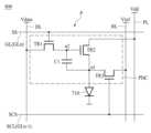
도 12는 본 발명의 또 다른 일 실시예에 따른 표시장치의 개략도이다.
도 13은 도 12의 어느 한 화소에 대한 회로도이다.
도 14는 도 13의 화소에 대한 평면도이다.
도 15는 도 14의 I-I'를 따라 자른 단면도이다.
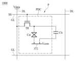
도 16은 본 발명의 또 다른 일 실시예에 따른 표시장치의 화소에 대한 회로도이다.
도 17은 본 발명의 또 다른 일 실시예에 따른 표시장치의 화소에 대한 회로도이다.
도 18은 본 발명의 또 다른 일 실시예에 따른 표시장치의 화소에 대한 회로도이다.FIG. 1 is a cross-sectional view of a thin film transistor according to one embodiment of the present invention.
Figure 2 is a schematic cross-sectional diagram to explain the surface state of the active layer.
Figure 3 is a graph showing the concentration of ions according to the depth of the active layer.
FIG. 4 is a cross-sectional view of a thin film transistor according to another embodiment of the present invention.
FIG. 5 is a cross-sectional view of a thin film transistor according to another embodiment of the present invention.
FIG. 6 is a cross-sectional view of a thin film transistor according to another embodiment of the present invention.
FIG. 7 is a cross-sectional view of a thin film transistor according to another embodiment of the present invention.
FIG. 8 is a cross-sectional view of a thin film transistor according to another embodiment of the present invention.
Figure 9 is a threshold voltage graph of thin film transistors.
Figures 10a to 10g are manufacturing process diagrams of a thin film transistor according to one embodiment of the present invention.
Figure 11a is a graph of the activation energy (Ea) of the active layer.
Figure 11b is a density of states (DOS) graph of the active layer.
Figure 12 is a schematic diagram of a display device according to another embodiment of the present invention.
Figure 13 is a circuit diagram for one pixel of Figure 12.
Figure 14 is a plan view of the pixels of Figure 13.
Figure 15 is a cross-sectional view taken along line I-I' of Figure 14.
FIG. 16 is a circuit diagram of a pixel of a display device according to another embodiment of the present invention.
FIG. 17 is a circuit diagram of a pixel of a display device according to another embodiment of the present invention.
FIG. 18 is a circuit diagram of a pixel of a display device according to another embodiment of the present invention.
본 발명의 이점 및 특징, 그리고 그것들을 달성하는 방법은 첨부되는 도면과 함께 상세하게 후술되어 있는 실시예들을 참조하면 명확해질 것이다. 그러나, 본 발명은 이하에서 개시되는 실시예들에 한정되는 것이 아니라 서로 다른 다양한 형태로 구현될 것이며, 단지 본 실시예들은 본 발명의 개시가 완전하도록 하며, 본 발명이 속하는 기술분야에서 통상의 지식을 가진 자에게 발명의 범주를 알려주기 위해 제공되는 것이다. 본 발명은 청구항의 범주에 의해 정의될 뿐이다.The advantages and features of the present invention, and the method for achieving them, will become clear with reference to the embodiments described in detail below together with the accompanying drawings. However, the present invention is not limited to the embodiments disclosed below, but may be implemented in various different forms, and these embodiments are provided only to make the disclosure of the present invention complete and to inform those skilled in the art of the scope of the invention. The present invention is defined only by the scope of the claims.
본 발명의 실시예들을 설명하기 위한 도면에 개시된 형상, 크기, 비율, 각도, 개수 등은 예시적인 것이므로, 본 발명이 도면에 도시된 사항에 한정되는 것은 아니다. 명세서 전체에 걸쳐 동일 구성 요소는 동일 참조 부호로 지칭될 수 있다. 또한, 본 발명을 설명함에 있어서, 관련된 공지 기술에 대한 구체적인 설명이 본 발명의 요지를 불필요하게 흐릴 수 있다고 판단되는 경우, 그 상세한 설명은 생략된다.The shapes, sizes, ratios, angles, numbers, etc. disclosed in the drawings for explaining embodiments of the present invention are exemplary, and the present invention is not limited to the matters illustrated in the drawings. The same components may be referred to by the same reference numerals throughout the specification. In addition, in explaining the present invention, if it is determined that a detailed description of a related known technology may unnecessarily obscure the gist of the present invention, the detailed description is omitted.
본 명세서에서 언급된 "포함한다", "갖는다", "이루어진다" 등이 사용되는 경우 "~만"이라는 표현이 사용되지 않는 이상 다른 부분이 추가될 수 있다. 구성 요소가 단수로 표현된 경우, 특별히 명시적인 기재 사항이 없는 한 복수를 포함한다.In this specification, when the words "includes," "has," "consists of," etc. are used, other parts may be added unless the expression "only" is used. When a component is expressed in the singular, the plural is included unless otherwise explicitly stated.
구성 요소를 해석함에 있어서, 별도의 명시적 기재가 없더라도 오차 범위를 포함하는 것으로 해석한다.When interpreting a component, it is interpreted as including the error range even if there is no separate explicit description.
예를 들어, "~상에", "~상부에", "~하부에", "~옆에" 등으로 두 부분의 위치 관계가 설명되는 경우, "바로" 또는 "직접"이라는 표현이 사용되지 않는 이상 두 부분 사이에 하나 이상의 다른 부분이 위치할 수 있다.For example, when the positional relationship between two parts is described as "on ~", "above ~", "below ~", "next to ~", etc., one or more other parts may be located between the two parts, unless the expression "right" or "directly" is used.
공간적으로 상대적인 용어인 "아래(below, beneath)", "하부 (lower)", "위(above)", "상부(upper)" 등은 도면에 도시되어 있는 바와 같이 하나의 소자 또는 구성 요소들과 다른 소자 또는 구성 요소들과의 상관관계를 용이하게 기술하기 위해 사용될 수 있다. 공간적으로 상대적인 용어는 도면에 도시되어 있는 방향에 더하여 사용시 또는 동작 시 소자의 서로 다른 방향을 포함하는 용어로 이해되어야 한다. 예를 들면, 도면에 도시되어 있는 소자를 뒤집을 경우, 다른 소자의 "아래(below)" 또는 "아래(beneath)"로 기술된 소자는 다른 소자의 "위(above)"에 놓일 수 있다. 따라서, 예시적인 용어인 "아래"는 아래와 위의 방향을 모두 포함할 수 있다. 마찬가지로, 예시적인 용어인 "위" 또는 "상"은 위와 아래의 방향을 모두 포함할 수 있다.The spatially relative terms "below," "beneath," "lower," "above," "upper," and the like can be used to easily describe the relationship of one element or component to another element or component, as illustrated in the drawings. The spatially relative terms should be understood to include different orientations of the elements during use or operation in addition to the orientations depicted in the drawings. For example, if an element illustrated in the drawings is flipped over, an element described as "below" or "beneath" another element may now be located "above" the other element. Thus, the exemplary term "below" can include both the above and below directions. Likewise, the exemplary term "above" or "above" can include both the above and below directions.
시간 관계에 대한 설명일 경우, 예를 들어, "~ 후에", "~ 에 이어서", "~ 다음에", "~ 전에" 등으로 시간적 선후 관계가 설명되는 경우, "바로" 또는 "직접"이라는 표현이 사용되지 않는 이상 연속적이지 않은 경우도 포함할 수 있다.When describing a temporal relationship, for example, when describing a temporal relationship such as "after", "following", "next to", "before", etc., it can also include cases where there is no continuity, as long as the expression "right away" or "directly" is not used.
제1, 제2 등이 다양한 구성요소들을 서술하기 위해서 사용되나, 이들 구성요소들은 이들 용어에 의해 제한되지 않는다. 이들 용어들은 단지 하나의 구성요소를 다른 구성요소와 구별하기 위하여 사용하는 것이다. 따라서, 이하에서 언급되는 제1 구성요소는 본 발명의 기술적 사상 내에서 제2 구성요소일 수도 있다.Although the terms first, second, etc. are used to describe various components, these components are not limited by these terms. These terms are only used to distinguish one component from another. Accordingly, a first component referred to below may also be a second component within the technical concept of the present invention.
"적어도 하나"의 용어는 하나 이상의 관련 항목으로부터 제시 가능한 모든 조합을 포함하는 것으로 이해되어야 한다. 예를 들어, "제1 항목, 제2 항목 및 제3 항목 중에서 적어도 하나"의 의미는 제1 항목, 제2 항목 또는 제3 항목 각각 뿐 아니라 제1 항목, 제2 항목 및 제3 항목 중에서 2개 이상으로부터 제시될 수 있는 모든 항목의 조합을 의미할 수 있다.The term "at least one" should be understood to include all combinations that can be presented from one or more of the associated items. For example, the meaning of "at least one of the first, second, and third items" can mean not only each of the first, second, or third items, but also all combinations of items that can be presented from two or more of the first, second, and third items.
본 발명의 여러 실시예들의 각각 특징들이 부분적으로 또는 전체적으로 서로 결합 또는 조합 가능하고, 기술적으로 다양한 연동 및 구동이 가능하며, 각 실시예들이 서로에 대하여 독립적으로 실시 가능할 수도 있고 연관 관계로 함께 실시될 수도 있다.The individual features of the various embodiments of the present invention may be partially or wholly combined or combined with each other, and may be technically linked and driven in various ways, and each embodiment may be implemented independently of each other or may be implemented together in a related relationship.
본 발명의 실시예들을 설명하는 각 도면의 구성요소들에 참조부호를 부가함에 있어서, 동일한 구성요소들에 대해서는 비록 다른 도면상에 표시되더라도 가능한 한 동일한 부호를 가질 수 있다.When adding reference numerals to components of each drawing describing embodiments of the present invention, identical components may have the same numerals as much as possible even if they are shown in different drawings.
본 발명의 실시예들에 있어서, 소스 전극과 드레인 전극은 설명의 편의를 위하여 구별한 것일 뿐, 소스 전극과 드레인 전극은 서로 바뀔 수 있다. 소스 전극이 드레인 전극이 되고, 드레인 전극이 소스 전극이 될 수 있다. 또한, 어느 한 실시예의 소스 전극은 다른 실시에에서 드레인 전극이 될 수 있고, 어느 한 실시예의 드레인 전극은 다른 실시예에서 소스 전극이 될 수 있다.In the embodiments of the present invention, the source electrode and the drain electrode are distinguished only for the convenience of explanation, and the source electrode and the drain electrode can be interchanged. The source electrode can become the drain electrode, and the drain electrode can become the source electrode. In addition, the source electrode of one embodiment can become the drain electrode in another embodiment, and the drain electrode of one embodiment can become the source electrode in another embodiment.
본 발명의 어떤 실시예에서는, 설명의 편의를 위해 소스 영역과 소스 전극을 구별하고 드레인 영역과 드레인 전극을 구별하기도 하지만, 본 발명의 실시예들이 이에 한정되는 것은 아니다. 소스 영역이 소스 전극이 될 수 있고, 드레인 영역이 드레인 전극이 될 수 있다. 또한, 소스 영역이 드레인 전극이 될 수도 있고, 드레인 영역이 소스 전극이 될 수도 있다.In some embodiments of the present invention, for convenience of explanation, the source region and the source electrode are distinguished, and the drain region and the drain electrode are distinguished, but the embodiments of the present invention are not limited thereto. The source region may be the source electrode, and the drain region may be the drain electrode. In addition, the source region may be the drain electrode, and the drain region may be the source electrode.
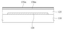
도 1은 본 발명의 일 실시예에 따른 박막 트랜지스터(100)의 단면도이다.FIG. 1 is a cross-sectional view of a thin film transistor (100) according to one embodiment of the present invention.
도 1를 참조하면, 본 발명의 일 실시예에 따른 박막 트랜지스터(100)는, 액티브층(130) 및 게이트 전극(160)을 포함한다. 또한, 본 발명의 일 실시예에 따른 박막 트랜지스터(100)는 소스 전극(151) 및 드레인 전극(152)을 포함한다. 액티브층(130) 및 게이트 전극(160)은 기판(110) 상에 배치된다.Referring to FIG. 1, a thin film transistor (100) according to one embodiment of the present invention includes an active layer (130) and a gate electrode (160). In addition, the thin film transistor (100) according to one embodiment of the present invention includes a source electrode (151) and a drain electrode (152). The active layer (130) and the gate electrode (160) are disposed on a substrate (110).
기판(110)은 유리 및 고분자 수지 중 적어도 하나를 포함할 수 있다. 예를 들어, 기판(110)으로 유리 기판 또는 고분자 수지 기판이 사용될 수 있다. 고분자 수지 기판으로 플라스틱 기판이 있다. 플라스틱 기판은, 플렉서블 특성을 갖는 투명 고분자 수지인 폴리이미드(PI), 폴리카보네이트(PC), 폴리에틸렌(PE), 폴리에스테르, 폴리에틸렌테레프탈레이트(PET) 및 폴리스트렌(PS) 중 적어도 하나를 포함할 수 있다.The substrate (110) may include at least one of glass and a polymer resin. For example, a glass substrate or a polymer resin substrate may be used as the substrate (110). A plastic substrate is included as the polymer resin substrate. The plastic substrate may include at least one of polyimide (PI), polycarbonate (PC), polyethylene (PE), polyester, polyethylene terephthalate (PET), and polystyrene (PS), which are transparent polymer resins having flexible properties.
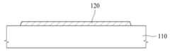
도 1을 참조하면, 기판(110) 상에 광차단층(120)이 배치될 수 있다. 광차단층(120)은 광을 차단하는 특성을 가질 수 있다. 광차단층(120)은 기판(110)으로부터 입사되는 광을 차단하여, 액티브층(130)을 보호할 수 있다.Referring to FIG. 1, a light-blocking layer (120) may be placed on a substrate (110). The light-blocking layer (120) may have a light-blocking property. The light-blocking layer (120) may block light incident from the substrate (110) and protect the active layer (130).
광차단층(120)은 금속을 포함할 수 있다. 광차단층(120)은 단일층으로 이루어질 수도 있고, 다층 구조를 가질 수도 있다.The light blocking layer (120) may include metal. The light blocking layer (120) may be formed of a single layer or may have a multilayer structure.
광차단층(120) 상에 버퍼층(125)이 배치될 수 있다. 버퍼층(125)은 광차단층(120)의 상면을 커버한다. 버퍼층(125)은 절연성을 가지며 액티브층(130)을 보호한다. 버퍼층(125)을 보호층 또는 절연층이라고도 한다.A buffer layer (125) may be placed on the light blocking layer (120). The buffer layer (125) covers the upper surface of the light blocking layer (120). The buffer layer (125) has insulating properties and protects the active layer (130). The buffer layer (125) is also called a protective layer or an insulating layer.
버퍼층(125)은 절연성을 갖는 실리콘 산화물(SiOx), 실리콘 질화물(SiNx), 하프늄 산화물(HfOx), 알루미늄 산화물(AlOx), 지르코늄 산화물(ZrOx), 하프늄 실리케이트 (Hf-SiOx) 및 지르코늄 실리케이트 (Zr-SiOx) 중 적어도 하나를 포함할 수 있다.The buffer layer (125) may include at least one of insulating silicon oxide (SiOx), silicon nitride (SiNx), hafnium oxide (HfOx), aluminum oxide (AlOx), zirconium oxide (ZrOx), hafnium silicate (Hf-SiOx), and zirconium silicate (Zr-SiOx).
도 1을 참조하면, 액티브층(130)은 버퍼층(125) 상에 배치된다. 액티브층(130)은 광차단층(120)과 중첩한다.Referring to Fig. 1, the active layer (130) is placed on the buffer layer (125). The active layer (130) overlaps the light blocking layer (120).
본 발명의 일 실시예에 따르면, 액티브층(130)은 산화물 반도체 물질을 포함할 수 있다. 본 발명의 일 실시예에 따르면, 액티브층(130)은, 예를 들어, 산화물 반도체 물질로 이루어진 산화물 반도체층일 수 있다.According to one embodiment of the present invention, the active layer (130) may include an oxide semiconductor material. According to one embodiment of the present invention, the active layer (130) may be, for example, an oxide semiconductor layer made of an oxide semiconductor material.
액티브층(130)은, IO(InO)계, ZO(ZnO)계, TO(SnO)계, GO(GaO)계, IZO(InZnO)계, IGO(InGaO)계, IGZO(InGaZnO)계, IGZTO(InGaZnSnO)계, GZTO(GaZnSnO)계, GZO(GaZnO)계, ITO(InSnO)계, ITZO(InSnZnO) 및 FIZO(FeInZnO)계 산화물 반도체 물질 중 적어도 하나를 포함할 수 있다.The active layer (130) may include at least one of oxide semiconductor materials selected from the group consisting of IO (InO)-based, ZO (ZnO)-based, TO (SnO)-based, GO (GaO)-based, IZO (InZnO)-based, IGO (InGaO)-based, IGZO (InGaZnO)-based, IGZTO (InGaZnSnO)-based, GZTO (GaZnSnO)-based, GZO (GaZnO)-based, ITO (InSnO)-based, ITZO (InSnZnO)-based, and FIZO (FeInZnO)-based.
액티브층(130)은 단일막 구조를 가질 수도 있고, 복수 개의 산화물 반도층으로 이루어진 다층막 구조를 가질 수도 있다(도 5 및 도 6 참조).The active layer (130) may have a single film structure or may have a multilayer film structure composed of multiple oxide semiconductor layers (see FIGS. 5 and 6).
본 발명의 일 실시예에 따르면, 액티브층(130)은 구리(Cu)를 포함한다.According to one embodiment of the present invention, the active layer (130) includes copper (Cu).
본 발명의 일 실시예에 따르면, 구리(Cu)는 이온 상태로 존재할 수 있다. 예를 들어, 액티브층(130)에서 구리(Cu)는 Cu2O 또는 CuO 상태로 존재할 수 있다. 구리(Cu)가 Cu2O 상태로 존재할 때, 구리(Cu)는 1가 이온(Cu+) 상태라고 할 수 있다. 구리(Cu)가 CuO 상태로 존재할 때, 구리(Cu)는 2가 이온(Cu2+) 상태라고 할 수 있다.According to one embodiment of the present invention, copper (Cu) may exist in an ionic state. For example, in the active layer (130), copper (Cu) may exist in a Cu2 O or CuO state. When copper (Cu) exists in a Cu2 O state, copper (Cu) may be said to be in a monovalent ion (Cu+ ) state. When copper (Cu) exists in a CuO state, copper (Cu) may be said to be in a divalent ion (Cu2+ ) state.
본 발명의 일 실시예에 따르면, "구리(Cu)"는 구리 원자 및 구리 이온(Cu+ 및 Cu2+) 모두 포함하는 의미이다.According to one embodiment of the present invention, “copper (Cu)” means both copper atoms and copper ions (Cu+ and Cu2+ ).
본 발명의 일 실시예에 따르면, 구리(Cu)는 액티브층(130)의 표면에 주로 배치된다. 보다 구체적으로, 구리(Cu)는 액티브층(130)의 상부 표면에 주로 배치될 수 있다. 본 발명의 일 실시예에 따르면, 액티브층(130)의 상부 표면은, 기판(110) 반대쪽의 액티브층(130)의 표면으로 정의된다.According to one embodiment of the present invention, copper (Cu) is mainly disposed on the surface of the active layer (130). More specifically, copper (Cu) may be mainly disposed on the upper surface of the active layer (130). According to one embodiment of the present invention, the upper surface of the active layer (130) is defined as the surface of the active layer (130) opposite the substrate (110).
본 발명의 일 실시예에 따르면, 액티브층(130)은 액티브층(130)의 두께 방향을 따라 구리(Cu)의 농도 구배(gradient)를 갖는다. 보다 구체적으로, 액티브층(130)의 두께 방향을 따라 구리(Cu)의 농도가 달라질 수 있다.According to one embodiment of the present invention, the active layer (130) has a copper (Cu) concentration gradient along the thickness direction of the active layer (130). More specifically, the concentration of copper (Cu) may vary along the thickness direction of the active layer (130).
본 발명의 일 실시예에 따르면, 액티브층(130)의 표면에서 구리(Cu)의 농도는 균일할 수 있다. 또한, 액티브층(130)의 표면으로부터 동일한 깊이에서 구리(Cu)의 농도가 동일할 수 있다.According to one embodiment of the present invention, the concentration of copper (Cu) on the surface of the active layer (130) may be uniform. In addition, the concentration of copper (Cu) at the same depth from the surface of the active layer (130) may be the same.
본 발명의 일 실시예에 따르면, 액티브층(130)은 기판(110) 상에 배치되며, 기판(110)을 향하는 방향을 따라, 액티브층(130) 내의 구리(Cu)의 농도가 작아질 수 있다.According to one embodiment of the present invention, the active layer (130) is disposed on the substrate (110), and the concentration of copper (Cu) in the active layer (130) may decrease along the direction toward the substrate (110).
도 2는 액티브층(130)의 표면 상태를 설명하기 위한 개략적인 단면도이다.Figure 2 is a schematic cross-sectional view for explaining the surface state of the active layer (130).
도 2를 참조하면, 액티브층(130)은 t0의 두께를 가질 수 있다. 액티브층(130)의 두께(t0)는, 액티브층(130)의 바닥면으로부터 액티브층(130)의 상부 표면 사이의 거리로 정의될 수 있다. 액티브층(130)의 바닥면은 버퍼층(125)의 상면과 동일하다. 액티브층(130)의 상부 표면은 기판(110) 반대쪽의 액티브층(130)의 표면이다.Referring to FIG. 2, the active layer (130) may have a thickness of t0. The thickness (t0) of the active layer (130) may be defined as a distance from a bottom surface of the active layer (130) to an upper surface of the active layer (130). The bottom surface of the active layer (130) is the same as the upper surface of the buffer layer (125). The upper surface of the active layer (130) is a surface of the active layer (130) opposite the substrate (110).
본 발명의 일 실시예에 따르면, 액티브층(130)의 깊이는 액티브층(130)의 상부 표면으로부터 기판(110)을 향하는 방향의 거리로 정의된다.According to one embodiment of the present invention, the depth of the active layer (130) is defined as the distance in the direction from the upper surface of the active layer (130) toward the substrate (110).
도 2의 L1, L2 및 L3는 액티브층(130)의 상부 표면의 서로 다른 지점에 해당된다. L1, L2 및 L3의 높이는 t0이고, L1, L2 및 L3의 깊이는 0이다. 도 2에서, L1, L2 및 L3의 깊이는 "dep0"로 표시된다.L1, L2, and L3 in Fig. 2 correspond to different points on the upper surface of the active layer (130). The heights of L1, L2, and L3 are t0, and the depths of L1, L2, and L3 are 0. In Fig. 2, the depths of L1, L2, and L3 are indicated as “dep0.”
본 발명의 일 실시예에 따르면, 액티브층(130)의 상부 표면의 서로 다른 지점인 L1, L2 및 L3에서 구리(Cu)의 농도는 서로 동일하다.According to one embodiment of the present invention, the concentrations of copper (Cu) at different points L1, L2 and L3 on the upper surface of the active layer (130) are the same.
도 2에서 L4, L5 및 L6의 높이는 t1이고, L4, L5 및 L6의 깊이는 dep1이다. L4, L5 및 L6은 L1, L2 및 L3보다 더 깊은 위치이다.In Fig. 2, the heights of L4, L5, and L6 are t1, and the depths of L4, L5, and L6 are dep1. L4, L5, and L6 are located deeper than L1, L2, and L3.
본 발명의 일 실시예에 따르면, L4, L5 및 L6에서 구리(Cu)의 농도는 서로 동일하다. L4, L5 및 L6의 구리(Cu)의 농도는 L1, L2 및 L3의 구리(Cu)의 농도보다 작다.According to one embodiment of the present invention, the concentrations of copper (Cu) in L4, L5 and L6 are equal to each other. The concentrations of copper (Cu) in L4, L5 and L6 are less than the concentrations of copper (Cu) in L1, L2 and L3.
도 2에서 L7, L8 및 L9의 높이는 t2이고, L7, L8 및 L9의 깊이는 dep2이다. L7, L8 및 L9는 L4, L5 및 L6보다 더 깊은 위치이다.In Fig. 2, the heights of L7, L8, and L9 are t2, and the depths of L7, L8, and L9 are dep2. L7, L8, and L9 are located deeper than L4, L5, and L6.
본 발명의 일 실시예에 따르면, L7, L8 및 L9에서 구리(Cu)의 농도는 서로 동일하다. L7, L8 및 L9의 구리(Cu)의 농도는 L4, L5 및 L6의 구리(Cu)의 농도보다 작다.According to one embodiment of the present invention, the concentrations of copper (Cu) in L7, L8 and L9 are equal to each other. The concentrations of copper (Cu) in L7, L8 and L9 are less than the concentrations of copper (Cu) in L4, L5 and L6.
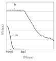
도 3은 액티브층(130)의 깊이에 따른 이온의 농도를 표시하는 그래프이다.Figure 3 is a graph showing the concentration of ions according to the depth of the active layer (130).
액티브층(130)의 깊이에 따른 이온의 농도는, 예를 들어, ToF-SIMS(Time of Flight Secondary Ion Mass Spectrometry)를 이용하는 깊이 프로파일(ToF-SIMS depth profile)에 의해 측정될 수 있다.The concentration of ions according to the depth of the active layer (130) can be measured, for example, by a depth profile (ToF-SIMS depth profile) using ToF-SIMS (Time of Flight Secondary Ion Mass Spectrometry).
본 발명의 일 실시예에 따르면, 구리(Cu)는 액티브층(130)의 두께 방향을 따라 도 3에 도시된 바와 같은 농도 구배(gradient)를 가질 수 있다. 구체적으로, 구리(Cu)는, 액티브층(130)의 두께 방향을 따라, 깊이가 깊어질수록 농도가 작아지는 양상으로, 농도 구배를 가질 수 있다. 또는, 액티브층(130)에서 구리(Cu)는, 기판(110)을 향하는 방향을 따라 농도가 작아지는 양상으로, 농도 구배를 가질 수 있다.According to one embodiment of the present invention, copper (Cu) may have a concentration gradient along the thickness direction of the active layer (130), as illustrated in FIG. 3. Specifically, copper (Cu) may have a concentration gradient in a manner that the concentration decreases as the depth increases along the thickness direction of the active layer (130). Alternatively, copper (Cu) in the active layer (130) may have a concentration gradient in a manner that the concentration decreases along the direction toward the substrate (110).
본 발명의 일 실시예에 따르면, 액티브층(130)의 하부, 예를 들어, L7, L8 및 L9 지점에는 구리(Cu)가 존재하지 않을 수도 있다.According to one embodiment of the present invention, copper (Cu) may not be present at the lower portion of the active layer (130), for example, at points L7, L8, and L9.
본 발명의 일 실시예에 따르면, 구리(Cu)는 주로 2가 이온(Cu2+) 상태로 존재할 수 있다. 구체적으로, 액티브층(130)의 구리(Cu)는 Cu+ 및 Cu2+를 포함한다. 본 발명의 일 실시예에 따르면, 액티브층(130)에서 Cu2+의 농도가 Cu+의 농도보다 높을 수 있다.According to one embodiment of the present invention, copper (Cu) may exist primarily in a divalent ion (Cu2+ ) state. Specifically, copper (Cu) of the active layer (130) includes Cu+ and Cu2+ . According to one embodiment of the present invention, the concentration of Cu2+ in the active layer (130) may be higher than the concentration of Cu+ .
본 발명의 일 실시예에 따르면, 액티브층(130) 상에 구리층을 형성한 후 구리층을 제거하여 구리 이온(Cu+ 또는 Cu2+)이 액티브층(130)에 잔존하도록 한 후, 열처리를 함으로써, 구리 이온이 주로 2가 이온(Cu2+) 상태로 존재하도록 할 수 있다. 본 발명의 일 실시예에 따르면, 구리(Cu)는 2가 이온(Cu2+) 상태로 산소와 결합하여 CuO 형태의 구리 산화물로 존재할 수 있다.According to one embodiment of the present invention, after forming a copper layer on an active layer (130), the copper layer is removed so that copper ions (Cu+ or Cu2+ ) remain in the active layer (130), and then heat treatment is performed so that the copper ions mainly exist in a divalent ion (Cu2+ ) state. According to one embodiment of the present invention, copper (Cu) can exist as a copper oxide in the form of CuO by combining with oxygen in a divalent ion (Cu2+ ) state.
산소와 결합된 구리(Cu)는 액티브층(130)에 인위적인 결함(defect)을 형성한 것과 같은 효과를 나타낼 수 있다. 이러한 결함을 유발할 수 있는 구리(Cu)는, 억셉터 유사 트랩(acceptor like trap)을 형성하여, 박막 트랜지스터(100)의 s-팩터(s-factor)를 증가시킬 수 있다.Copper (Cu) combined with oxygen can have the same effect as forming an artificial defect in the active layer (130). Copper (Cu) that can cause such a defect can form an acceptor like trap, thereby increasing the s-factor of the thin film transistor (100).
본 발명의 일 실시예에 따르면, 액티브층(130)에 구리가 소량으로 포함되기 때문에, 구리(Cu)에 의한 전류 특성 저하가 최소화될 수 있다. 그 결과, 박막 트랜지스터(100)의 전기적 특성 저하 없이, 박막 트랜지스터(100)의 s-팩터(s-factor)를 증가시킬 수 있다.According to one embodiment of the present invention, since a small amount of copper is included in the active layer (130), the deterioration of current characteristics due to copper (Cu) can be minimized. As a result, the s-factor of the thin film transistor (100) can be increased without deteriorating the electrical characteristics of the thin film transistor (100).
또한, 구리(Cu)가 산소와 결합하여 CuO와 같은 안정적인 결합을 형성할 수 있기 때문에, 액티브층(130)의 안정성이 향상될 수 있고, 그 결과, 박막 트랜지스터(100)의 안정성이 향상될 수 있다.In addition, since copper (Cu) can combine with oxygen to form a stable bond such as CuO, the stability of the active layer (130) can be improved, and as a result, the stability of the thin film transistor (100) can be improved.
본 발명의 일 실시예에 따르면, 액티브층(130)의 구리(Cu) 농도는 0.1 내지 0.18 원자%(at %)일 수 있다. 여기서, 원자%(at %)는, 액티브층(130)을 구성하는 전체 금속 원자 수 대비 구리(Cu)의 원자 수 비율로 계산될 수 있다. 액티브층(130)을 구성하는 전체 금속 원자 수는 산소(O)의 원자 수를 포함하지 않는다. 액티브층(130)을 구성하는 각 금속의 원자%(at %)는 ToF-SIMS(Time of Flight Secondary Ion Mass Spectrometry)를 이용하는 깊이 프로파일(ToF-SIMS depth profile)에 의해 계산될 수 있다.According to one embodiment of the present invention, the copper (Cu) concentration of the active layer (130) may be 0.1 to 0.18 atomic % (at %). Here, the atomic % (at %) may be calculated as the ratio of the number of copper (Cu) atoms to the total number of metal atoms constituting the active layer (130). The total number of metal atoms constituting the active layer (130) does not include the number of oxygen (O) atoms. The atomic % (at %) of each metal constituting the active layer (130) may be calculated by a depth profile using ToF-SIMS (Time of Flight Secondary Ion Mass Spectrometry).
액티브층(130)의 구리(Cu) 농도가 0.1 원자%(at %) 미만인 경우, 구리(Cu)에 의한 결함(defect) 형성 및 s-팩터 증가 효과가 거의 나타나지 않을 수 있고, 박막 트랜지스터(100)의 안정성 향상 효과가 미미할 수 있다. 반면, 액티브층(130)의 구리(Cu) 농도가 0.18 원자%(at %)를 초과하는 경우, 박막 트랜지스터(100)의 전류 특성 및 전기적 특성이 저하될 수 있다.When the copper (Cu) concentration of the active layer (130) is less than 0.1 at% (at%), the defect formation and s-factor increase effects due to copper (Cu) may hardly appear, and the stability improvement effect of the thin film transistor (100) may be minimal. On the other hand, when the copper (Cu) concentration of the active layer (130) exceeds 0.18 at% (at%), the current characteristics and electrical characteristics of the thin film transistor (100) may deteriorate.
본 발명의 일 실시예에 따르면, 액티브층(130)은 채널부(131), 제1 연결부(132) 및 제2 연결부(133)을 포함한다. 액티브층(130)의 선택적 도체화에 의하여 제1 연결부(132) 및 제2 연결부(133)가 형성될 수 있다. 제1 연결부(132) 및 제2 연결부(133)는 일반적으로 채널부(131)의 양쪽에 배치된다.According to one embodiment of the present invention, the active layer (130) includes a channel portion (131), a first connection portion (132), and a second connection portion (133). The first connection portion (132) and the second connection portion (133) can be formed by selectively conducting the active layer (130). The first connection portion (132) and the second connection portion (133) are generally arranged on both sides of the channel portion (131).
채널부(131)는 반도체 특성을 갖는다. 채널부(131)는 광차단층(120)과 중첩한다. 광차단층(120)은 기판(110)으로부터 입사되는 광이 액티브층(130)의 채널부(131)에 도달하는 것을 방지하여, 채널부(131)를 보호할 수 있다. 또한, 채널부(131)는 게이트 전극(160)과 중첩한다.The channel portion (131) has semiconductor characteristics. The channel portion (131) overlaps with the light-blocking layer (120). The light-blocking layer (120) can prevent light incident from the substrate (110) from reaching the channel portion (131) of the active layer (130), thereby protecting the channel portion (131). In addition, the channel portion (131) overlaps with the gate electrode (160).
액티브층(130) 상에 게이트 절연막(140)이 배치된다. 게이트 절연막(140)은 실리콘 산화물(SiOx), 실리콘 질화물(SiNx), 하프늄 산화물(HfOx), 알루미늄 산화물(AlOx), 지르코늄 산화물(ZrOx), 하프늄 실리케이트 (Hf-SiOx), 지르코늄 실리케이트 (Zr-SiOx) 중 적어도 하나를 포함할 도 있다. 게이트 절연막(140)은 단일막 구조를 가질 수도 있고, 다층막 구조를 가질 수도 있다.A gate insulating film (140) is disposed on the active layer (130). The gate insulating film (140) may include at least one of silicon oxide (SiOx), silicon nitride (SiNx), hafnium oxide (HfOx), aluminum oxide (AlOx), zirconium oxide (ZrOx), hafnium silicate (Hf-SiOx), and zirconium silicate (Zr-SiOx). The gate insulating film (140) may have a single-film structure or a multilayer film structure.
게이트 절연막(140) 상에 게이트 전극(160)이 배치된다. 게이트 전극(160)은 액티브층(130)과 이격되어, 액티브층(130)과 적어도 일부 중첩한다. 게이트 전극(160)은 액티브층(130)의 채널부(131)와 중첩한다.A gate electrode (160) is arranged on a gate insulating film (140). The gate electrode (160) is spaced apart from the active layer (130) and overlaps at least partially with the active layer (130). The gate electrode (160) overlaps with the channel portion (131) of the active layer (130).
게이트 전극(160)은 알루미늄(Al)이나 알루미늄 합금과 같은 알루미늄 계열의 금속, 은(Ag)이나 은 합금과 같은 은 계열의 금속, 구리(Cu)나 구리 합금과 같은 구리 계열의 금속, 몰리브덴(Mo)이나 몰리브덴 합금과 같은 몰리브덴 계열의 금속, 크롬(Cr), 탄탈륨(Ta), 네오듐(Nd) 및 티타늄(Ti) 중 적어도 하나를 포함할 수 있다. 게이트 전극(160)은 물리적 성질이 다른 적어도 두 개의 도전막을 포함하는 다층막 구조를 가질 수도 있다.The gate electrode (160) may include at least one of an aluminum series metal such as aluminum (Al) or an aluminum alloy, a silver series metal such as silver (Ag) or a silver alloy, a copper series metal such as copper (Cu) or a copper alloy, a molybdenum series metal such as molybdenum (Mo) or a molybdenum alloy, chromium (Cr), tantalum (Ta), neodymium (Nd), and titanium (Ti). The gate electrode (160) may also have a multilayer film structure including at least two conductive films having different physical properties.
게이트 전극(160) 상에 층간 절연막(170)이 배치된다. 층간 절연막(170)은 절연 물질로 이루어진 절연층이다. 구체적으로, 층간 절연막(170)은 유기물로 이루어질 수도 있고, 무기물로 이루어질 수도 있으며, 유기물층과 무기물층의 적층체로 이루어질 수도 있다.An interlayer insulating film (170) is placed on the gate electrode (160). The interlayer insulating film (170) is an insulating layer made of an insulating material. Specifically, the interlayer insulating film (170) may be made of an organic material, an inorganic material, or a laminate of an organic material layer and an inorganic material layer.
층간 절연막(170) 상에 소스 전극(151) 및 드레인 전극(152)이 배치된다. 소스 전극(151)과 드레인 전극(152)은 서로 이격되어 각각 액티브층(130)과 연결된다. 소스 전극(151)과 드레인 전극(152)은 층간 절연막(170)에 형성된 콘택홀을 통하여 각각 액티브층(130)과 연결된다.A source electrode (151) and a drain electrode (152) are arranged on an interlayer insulating film (170). The source electrode (151) and the drain electrode (152) are spaced apart from each other and are each connected to an active layer (130). The source electrode (151) and the drain electrode (152) are each connected to the active layer (130) through a contact hole formed in the interlayer insulating film (170).
소스 전극(151) 및 드레인 전극(152)은 각각 몰리브덴(Mo), 알루미늄(Al), 크롬(Cr), 금(Au), 티타늄(Ti), 니켈(Ni), 네오듐(Nd), 구리(Cu), 및 이들의 합금 중 적어도 하나를 포함할 수 있다. 소스 전극(151) 및 드레인 전극(152)은 각각 금속 또는 금속의 합금으로 된 단일층으로 이루어질 수도 있고, 2층 이상의 다층으로 이루어질 수도 있다.The source electrode (151) and the drain electrode (152) may each include at least one of molybdenum (Mo), aluminum (Al), chromium (Cr), gold (Au), titanium (Ti), nickel (Ni), neodymium (Nd), copper (Cu), and alloys thereof. The source electrode (151) and the drain electrode (152) may each be formed of a single layer made of a metal or an alloy of metals, or may be formed of two or more multilayers.
본 발명의 일 실시예에 따르면, 게이트 전극(160)을 마스크로 하는 선택적 도체화에 의하여, 액티브층(130)이 선택적으로 도체화될 수 있다.According to one embodiment of the present invention, the active layer (130) can be selectively conductive by selective conductive using the gate electrode (160) as a mask.
액티브층(130) 중 게이트 전극(160)과 중첩하는 영역은 도체화되지 않아 채널부(131)가 된다. 액티브층(130) 중 게이트 전극(160)과 중첩하지 않는 영역은 도체화되어 제1 연결부(132) 및 제2 연결부(133)가 된다.The region of the active layer (130) that overlaps with the gate electrode (160) is not conductive and becomes a channel portion (131). The region of the active layer (130) that does not overlap with the gate electrode (160) is conductive and becomes a first connection portion (132) and a second connection portion (133).
본 발명의 일 실시예에 따르면, 예를 들어, 플라즈마 처리 또는 드라이 에치에 의하여 액티브층(130)이 선택적으로 도체화될 수 있다. 그러나, 본 발명의 일 실시예가 이에 한정되는 것은 아니며, 도펀트를 이용하는 도핑에 의하여 액티브층(130)이 선택적으로 도체화될 수 있다. 이 때, 도핑된 영역이 도체화된다. 도핑을 위하여, 예를 들어, 붕소(B) 이온, 인(P) 이온, 비소(As) 이온 및 안티모니(Sb) 이온 중 적어도 하나에 의하여 도핑이 이루어질 수 있다. 또한, 광조사에 의하여 액티브층(130)이 선택적으로 도체화될 수도 있다.According to one embodiment of the present invention, the active layer (130) can be selectively made conductive, for example, by plasma treatment or dry etching. However, one embodiment of the present invention is not limited thereto, and the active layer (130) can be selectively made conductive by doping using a dopant. At this time, the doped region is made conductive. For doping, doping can be performed, for example, by at least one of boron (B) ions, phosphorus (P) ions, arsenic (As) ions, and antimony (Sb) ions. In addition, the active layer (130) can also be selectively made conductive by light irradiation.
본 발명의 일 실시예에 따르면, 제1 연결부(132) 및 제2 연결부(133) 중 어느 하나는 소스 영역이 되고, 다른 하나는 드레인 영역이 될 수 있다. 소스 영역은 소스 전극(151)과 연결되는 소스 연결부 역할을 할 수 있다. 드레인 영역은 드레인 전극(152)과 연결되는 드레인 연결부 역할을 할 수 있다.According to one embodiment of the present invention, one of the first connecting portion (132) and the second connecting portion (133) may be a source region, and the other may be a drain region. The source region may serve as a source connecting portion connected to the source electrode (151). The drain region may serve as a drain connecting portion connected to the drain electrode (152).
도면에 도시된 제1 연결부(132)와 제2 연결부(133)는 설명의 편의를 위하여 구별된 것일 뿐, 제1 연결부(132)와 제2 연결부(133)는 서로 바뀔 수도 있다. 제1 연결부(132)가 소스 영역이 되고, 제2 연결부(133)가 드레인 영역이 될 수 있다. 또한, 제1 연결부(132)가 드레인 영역이 되고, 제2 연결부(133)가 소스 영역이 될 수도 있다.The first connection part (132) and the second connection part (133) shown in the drawing are only distinguished for convenience of explanation, and the first connection part (132) and the second connection part (133) may be interchanged. The first connection part (132) may become a source region, and the second connection part (133) may become a drain region. In addition, the first connection part (132) may become a drain region, and the second connection part (133) may become a source region.
본 발명의 일 실시예에 따르면, 제1 연결부(132)가 소스 전극 역할을 할 수도 있고, 드레인 전극 역할을 할 수도 있다. 또한, 제2 연결부(133)가 드레인 전극 역할을 할 수도 있고, 소스 전극 역할을 할 수도 있다.According to one embodiment of the present invention, the first connecting portion (132) may serve as a source electrode or a drain electrode. Additionally, the second connecting portion (133) may serve as a drain electrode or a source electrode.
액티브층(130), 게이트 전극(160), 소스 전극(151) 및 드레인 전극(152)에 의하여 박막 트랜지스터(TFT)가 형성된다. 도 1에 도시된 바와 같이, 게이트 전극(160)이 액티브층(130)의 상부에 배치된 박막 트랜지스터를 탑 게이트 구조의 박막 트랜지스터(TFT)라고도 한다.A thin film transistor (TFT) is formed by an active layer (130), a gate electrode (160), a source electrode (151), and a drain electrode (152). As shown in Fig. 1, a thin film transistor in which the gate electrode (160) is positioned on top of the active layer (130) is also called a thin film transistor (TFT) with a top gate structure.
본 발명의 일 실시예에 따르면, 미량의 구리(Cu)가 주로 액티브층(130)의 표면에서 주로 2가 이온(Cu2+) 상태로 존재하도록 함으로써, 전기적 특성 및 신뢰성 저하 없이, 박막 트랜지스터(100)의 s-팩터(s-factor)를 증가시키고, 박막 트랜지스터(100)의 안정성을 향상시킬 수 있다.According to one embodiment of the present invention, by allowing a small amount of copper (Cu) to exist mainly in a divalent ion (Cu2+ ) state on the surface of the active layer (130), the s-factor of the thin film transistor (100) can be increased and the stability of the thin film transistor (100) can be improved without deteriorating electrical characteristics and reliability.
도 4는 본 발명의 다른 일 실시예에 따른 박막 트랜지스터(200)의 단면도이다.FIG. 4 is a cross-sectional view of a thin film transistor (200) according to another embodiment of the present invention.
도 4를 참조하면, 게이트 절연막(140)이 패턴화되지 않고, 액티브층(130)의 상면 전체를 커버할 수 있다. 또한, 게이트 절연막(140)은 콘택홀 영역을 제외하고 기판(110)의 상부 전체를 커버할 수 있다.Referring to FIG. 4, the gate insulating film (140) is not patterned and can cover the entire upper surface of the active layer (130). In addition, the gate insulating film (140) can cover the entire upper portion of the substrate (110) except for the contact hole region.
게이트 절연막(140)이 패턴화되지 않고, 액티브층(130)의 상면 전체를 커버하는 경우, 도펀트를 이용하는 도핑에 의하여 액티브층(130)이 선택적으로 도체화될 수 있다. 그 결과, 게이트 절연막(140)이 패턴화되지 않더라도 액티브층(130)의 제1 연결부(132) 및 제2 연결부(133)가 형성될 수 있다.When the gate insulating film (140) is not patterned and covers the entire upper surface of the active layer (130), the active layer (130) can be selectively made conductive by doping using a dopant. As a result, the first connection portion (132) and the second connection portion (133) of the active layer (130) can be formed even if the gate insulating film (140) is not patterned.
도 5는 본 발명의 또 다른 일 실시예에 따른 박막 트랜지스터(300)의 단면도이다.FIG. 5 is a cross-sectional view of a thin film transistor (300) according to another embodiment of the present invention.
도 5를 참조하면, 액티브층(130)은 제1 산화물 반도체층(130a) 및 제1 산화물 반도체층(130a) 상의 제2 산화물 반도체층(130b)을 포함한다.Referring to FIG. 5, the active layer (130) includes a first oxide semiconductor layer (130a) and a second oxide semiconductor layer (130b) on the first oxide semiconductor layer (130a).
제1 산화물 반도체층(130a)은 버퍼층(125) 상에 배치되며, 제2 산화물 반도체층(130b)을 지지하는 지지층 역할을 할 수 있다. 제2 산화물 반도체층(130b)는 메인 채널층 역할을 할 수 있다.The first oxide semiconductor layer (130a) is disposed on the buffer layer (125) and can serve as a support layer supporting the second oxide semiconductor layer (130b). The second oxide semiconductor layer (130b) can serve as a main channel layer.
지지층 역할을 하는 제1 산화물 반도체층(130a)은 우수한 막 안정성 및 기계적 안정성을 가질 수 있다. 제1 산화물 반도체층(130a)은, 예를 들어, IGZO (InGaZnO)계, IGO(InGaO)계, IGZTO(InGaZnSnO)계, GZTO(GaZnSnO)계, GZO(GaZnO)계 및 GO(GaO)계 산화물 반도체 물질 중 적어도 하나를 포함할 수 있다. 그러나, 본 발명의 일 실시예가 이에 한정되는 것은 아니며, 당업계에 알려진 다른 산화물 반도체 물질에 의하여 제1 산화물 반도체층(130a)이 만들어질 수 있다.The first oxide semiconductor layer (130a) serving as a support layer may have excellent film stability and mechanical stability. The first oxide semiconductor layer (130a) may include, for example, at least one of an IGZO (InGaZnO)-based, IGO (InGaO)-based, IGZTO (InGaZnSnO)-based, GZTO (GaZnSnO)-based, GZO (GaZnO)-based, and GO (GaO)-based oxide semiconductor material. However, one embodiment of the present invention is not limited thereto, and the first oxide semiconductor layer (130a) may be made of other oxide semiconductor materials known in the art.
제2 산화물 반도체층(130b)은, 예를 들어, IZO(InZnO)계, TO(SnO)계, IO(InO)계, IGO(InGaO)계, ITO(InSnO)계, IGZO(InGaZnO)계, IGZTO(InGaZnSnO)계, GZTO(GaZnSnO)계, ITZO(InSnZnO)계, FIZO(FeInZnO)계 등의 산화물 반도체 물질에 의해 만들어질 수 있다. 그러나, 본 발명의 일 실시예가 이에 한정되는 것은 아니며, 당업계에 알려진 다른 산화물 반도체 물질에 의하여 제2 산화물 반도체층(130b)이 만들어질 수 있다.The second oxide semiconductor layer (130b) may be made of, for example, an oxide semiconductor material such as an IZO (InZnO) system, a TO (SnO) system, an IO (InO) system, an IGO (InGaO) system, an ITO (InSnO) system, an IGZO (InGaZnO) system, an IGZTO (InGaZnSnO) system, a GZTO (GaZnSnO) system, an ITZO (InSnZnO) system, or a FIZO (FeInZnO) system. However, one embodiment of the present invention is not limited thereto, and the second oxide semiconductor layer (130b) may be made of other oxide semiconductor materials known in the art.
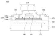
도 6은 본 발명의 또 다른 일 실시예에 따른 박막 트랜지스터(400)의 단면도이다.FIG. 6 is a cross-sectional view of a thin film transistor (400) according to another embodiment of the present invention.
도 6에 도시된 박막 트랜지스터(400)는, 도 5에 도시된 박막 트랜지스터(300)와 비교하여, 제2 산화물 반도체층(130b) 상의 제3 산화물 반도체층(130c)을 더 포함한다. 제3 산화물 반도체층(130c)은 산화물 반도체 물질로 만들어질 수 있다. 제3 산화물 반도체층(130c)은 제1 산화물 반도체층(130a)과 동일한 물질로 만들어질 수도 있다.The thin film transistor (400) illustrated in FIG. 6 further includes a third oxide semiconductor layer (130c) on the second oxide semiconductor layer (130b), compared to the thin film transistor (300) illustrated in FIG. 5. The third oxide semiconductor layer (130c) may be made of an oxide semiconductor material. The third oxide semiconductor layer (130c) may also be made of the same material as the first oxide semiconductor layer (130a).
도 7은 본 발명의 또 다른 일 실시예에 따른 박막 트랜지스터(500)의 단면도이다.FIG. 7 is a cross-sectional view of a thin film transistor (500) according to another embodiment of the present invention.
도 7의 박막 트랜지스터(500)는 기판(110) 상의 게이트 전극(160), 게이트 전극(160) 상의 게이트 절연막(140), 게이트 절연막(140) 상의 액티브층(130), 액티브층(130)과 연결된 소스 전극(151) 및 소스 전극(151)과 이격되어 액티브층(130)과 연결된 드레인 전극(152)을 포함한다. 도 7을 참조하면, 박막 트랜지스터(500)는 에치 스토퍼(145)를 더 포함할 수 있다.The thin film transistor (500) of FIG. 7 includes a gate electrode (160) on a substrate (110), a gate insulating film (140) on the gate electrode (160), an active layer (130) on the gate insulating film (140), a source electrode (151) connected to the active layer (130), and a drain electrode (152) spaced apart from the source electrode (151) and connected to the active layer (130). Referring to FIG. 7, the thin film transistor (500) may further include an etch stopper (145).
액티브층(130)은 산화물 반도체 물질을 포함할 수 있다.The active layer (130) may include an oxide semiconductor material.
도 7을 참조하면, 게이트 전극(160)이 기판(110)과 액티브층(130) 사이에 배치된다. 도 7에 도시된 바와 같이, 게이트 전극(160)이 액티브층(130)의 아래에 배치된 구조를 바텀 게이트(bottom gate) 구조라고도 한다. 액티브층(130)은 구리(Cu)를 포함할 수 있다. 액티브층(130)에 포함된 구리(Cu)는 이미 설명되었으므로, 중복을 피하기 위하여 구리(Cu)에 대한 상세한 설명은 생략된다.Referring to FIG. 7, a gate electrode (160) is disposed between the substrate (110) and the active layer (130). As illustrated in FIG. 7, a structure in which the gate electrode (160) is disposed below the active layer (130) is also referred to as a bottom gate structure. The active layer (130) may include copper (Cu). Since the copper (Cu) included in the active layer (130) has already been described, a detailed description of the copper (Cu) is omitted to avoid duplication.
도 8은 본 발명의 또 다른 일 실시예에 따른 박막 트랜지스터(600)의 단면도이다.FIG. 8 is a cross-sectional view of a thin film transistor (600) according to another embodiment of the present invention.
도 8에 도시된 바와 같이, 액티브층(130)은 제1 산화물 반도체층(130a) 및 제1 산화물 반도체층(130a) 상의 제2 산화물 반도체층(130b)을 포함할 수 있다. 그러나, 본 발명의 또 다른 일 실시예가 이에 한정되는 것은 아니며, 액티브층(130)은 제2 산화물 반도체층(130b) 상에 배치된 제3 산화물 반도체층(130c)을 더 포함할 수도 있다.As illustrated in FIG. 8, the active layer (130) may include a first oxide semiconductor layer (130a) and a second oxide semiconductor layer (130b) on the first oxide semiconductor layer (130a). However, another embodiment of the present invention is not limited thereto, and the active layer (130) may further include a third oxide semiconductor layer (130c) disposed on the second oxide semiconductor layer (130b).
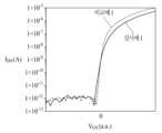
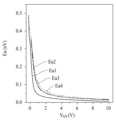
이하, 도 9를 참조하여, s-팩터(s-factor)를 설명한다.Below, the s-factor is explained with reference to Fig. 9.
도 9는 박막 트랜지스터들의 문턱전압 그래프이다.Figure 9 is a threshold voltage graph of thin film transistors.
도 9에서 "실시예 1"은 구리(Cu)를 포함하는 액티브층(130)을 갖는 본 발명의 일 실시예에 따른 박막 트랜지스터의 문턱전압 그래프를 지칭한다. 도 9에서 "비교예 1"은 구리(Cu)를 포함하지 않는 액티브층(130)을 갖는 박막 트랜지스터의 문턱전압 그래프를 지칭한다.In FIG. 9, “Example 1” refers to a threshold voltage graph of a thin film transistor according to one embodiment of the present invention having an active layer (130) including copper (Cu). In FIG. 9, “Comparative Example 1” refers to a threshold voltage graph of a thin film transistor having an active layer (130) that does not include copper (Cu).
도 9의 문턱전압 그래프는 박막 트랜지스터의 게이트 전압(VGS)에 대한 드레인-소스 전류(IDS)의 값으로 표시된다.The threshold voltage graph in Fig. 9 is expressed as the value of the drain-source current (IDS ) versus the gate voltage (VGS ) of the thin film transistor.
s-팩터(sub-threshold swing: s-factor)는 박막 트랜지스터의 게이트 전압(Gate Voltage; VGS)에 대한 드레인-소스 전류(Drain-Source Current; IDS) 그래프에 있어서, 문턱전압(Vth) 구간에서 그래프의 기울기의 역수값으로 구해진다. s-팩터는, 예를 들어, 박막 트랜지스터의 문턱전압(Vth 또는 V0) 구간에서, 게이트 전압에 대한 드레인-소스 전류의 변화 정도를 나타내는 지표로 사용될 수 있다.The s-factor (sub-threshold swing: s-factor) is the reciprocal of the slope of the graph of the drain-source current (IDS ) versus the gate voltage (VGS ) of a thin film transistor in the threshold voltage (Vth) section. The s-factor can be used, for example, as an indicator of the degree of change in the drain-source current with respect to the gate voltage in the threshold voltage (Vth or V0) section of a thin film transistor.
s-팩터가 커지면, 문턱전압(Vth) 구간에서 게이트 전압에 대한 드레인-소스 전류(IDS) 변화율이 완만해진다.As the s-factor increases, the rate of change of drain-source current (IDS ) with respect to the gate voltage in the threshold voltage (Vth) range becomes more gradual.
도 9는 게이트 전압(VGS)에 대한 드레인-소스 전류(IDS)를 표시하고 있다. 도 9에 도시된 그래프의 문턱전압(Vth) 구간에서, 게이트 전압(VGS)에 대한 드레인-소스 전류(IDS) 그래프 기울기의 역수가 s-팩터이다. s-팩터가 크면, 문턱전압(Vth) 구간에서 게이트 전압에 대한 드레인-소스 전류(IDS) 변화율이 완만하다.Figure 9 shows the drain-source current (IDS ) versus the gate voltage (VGS ). In the threshold voltage (Vth) section of the graph illustrated in Figure 9, the inverse of the slope of the drain-source current (IDS ) versus the gate voltage (VGS ) graph is the s-factor. When the s-factor is large, the rate of change of the drain-source current (IDS ) versus the gate voltage in the threshold voltage (Vth) section is gradual.
s-팩터가 커지면, 문턱전압(Vth) 구간에서 게이트 전압에 대한 드레인-소스 전류(IDS) 변화율이 완만해지기 때문에, 게이트 전압(VGS)을 조절하는 것에 의하여 드레인-소스 전류(IDS)의 크기를 조절하는 것이 용이해진다.As the s-factor increases, the rate of change of the drain-source current (IDS ) with respect to the gate voltage in the threshold voltage (Vth) range becomes more gradual, making it easier to control the size of the drain-source current (IDS ) by controlling the gate voltage (VGS ).
전류에 의해 구동되는 표시장치, 예를 들어, 유기발광 표시장치에서, 화소의 계조는 구동 소자인 구동 박막 트랜지스터의 드레인-소스 전류(IDS)의 크기를 조절하는 것에 의하여 제어될 수 있다. 구동 박막 트랜지스터의 드레인-소스 전류(IDS)의 크기는 게이트 전압에 의하여 결정된다. 따라서, 전류에 의해 구동되는 유기발광 표시장치에서, 구동 박막 트랜지스터(driving TFT)의 s-팩터(s-factor)가 클수록, 게이트 전압을 조정하여 화소의 계조(gray scale)를 조정하는 것이 용이하다.In a current-driven display device, for example, an organic light-emitting display device, the gray scale of a pixel can be controlled by adjusting the magnitude of a drain-source current (IDS ) of a driving thin film transistor, which is a driving element. The magnitude of the drain-source current (IDS ) of the driving thin film transistor is determined by a gate voltage. Therefore, in a current-driven organic light-emitting display device, the larger the s-factor of the driving thin film transistor (driving TFT), the easier it is to adjust the gray scale of a pixel by adjusting the gate voltage.
도 9를 참조하면, 문턱전압(0V) 근처에서, 실시예 1에 따른 박막 트랜지스터의 문턱전압 그래프보다 비교예 1에 따른 박막 트랜지스터의 문턱전압 그래프의 기울기가 더 크다는 것을 확인할 수 있다.Referring to FIG. 9, it can be confirmed that near the threshold voltage (0 V), the slope of the threshold voltage graph of the thin film transistor according to Comparative Example 1 is greater than that of the threshold voltage graph of the thin film transistor according to Example 1.
문턱전압(0V) 근처에서, 실시예 1에 따른 박막 트랜지스터의 드레인-소스 전류(IDS) 변화율이 비교예 1에 따른 박막 트랜지스터의 드레인-소스 전류(IDS) 변화율보다 작다. 도 9를 참조하면, 본 발명의 일 실시예에 따른 박막 트랜지스터(100)는 0.2 이상의 s-팩터를 가질 수 있다. 0.2 이상의 s-팩터를 갖는 본 발명의 일 실시예에 따른 박막 트랜지스터(100)를 이용하는 경우, 표시장치의 계조를 용이하게 조정할 수 있다.Near the threshold voltage (0 V), the drain-source current (IDS ) change rate of the thin film transistor according to Example 1 is smaller than the drain-source current (IDS ) change rate of the thin film transistor according to Comparative Example 1. Referring to FIG. 9, the thin film transistor (100) according to an embodiment of the present invention may have an s-factor of 0.2 or more. When the thin film transistor (100) according to an embodiment of the present invention having an s-factor of 0.2 or more is used, the grayscale of the display device can be easily adjusted.
구체적으로, 실시예 1과 같은 본 발명의 일 실시예에 따른 박막 트랜지스터(100)가 표시장치에 적용되는 경우, 게이트 전압을 조정하는 것에 의하여 드레인-소스 전류(IDS)의 크기를 용이하게 조절할 수 있고, 그 결과, 화소의 계조(gray scale)를 용이하게 조정할 수 있다.Specifically, when a thin film transistor (100) according to one embodiment of the present invention, such as Example 1, is applied to a display device, the size of the drain-source current (IDS ) can be easily controlled by adjusting the gate voltage, and as a result, the gray scale of a pixel can be easily controlled.
이하, 도 10a 내지 10g를 참조하며, 본 발명의 일 실시예에 따른 박막 트랜지스터(100)의 제조방법을 설명한다.Hereinafter, with reference to FIGS. 10a to 10g, a method for manufacturing a thin film transistor (100) according to one embodiment of the present invention will be described.
도 10a 내지 10g는 본 발명의 일 실시예에 따른 박막 트랜지스터의 제조 공정도이다.Figures 10a to 10g are manufacturing process diagrams of a thin film transistor according to one embodiment of the present invention.
도 10a을 참조하면, 기판(110) 상에 광차단층(120)이 형성된다.Referring to Fig. 10a, a light blocking layer (120) is formed on a substrate (110).
도 10b를 참조하면, 광차단층(120) 상에 버퍼층(125)이 형성되고, 버퍼층(125) 상에 액티브 물질층(130m)이 형성된다. 또한, 액티브 물질층(130m) 상에 구리층(135m)이 형성된다.Referring to Fig. 10b, a buffer layer (125) is formed on a light-blocking layer (120), and an active material layer (130m) is formed on the buffer layer (125). In addition, a copper layer (135m) is formed on the active material layer (130m).
액티브 물질층(130m)은 산화물 반도체 물질을 포함할 수 있다. 액티브 물질층(130m)은 산화물 반도체 물질에 의하여 형성될 수 있다. 액티브 물질층(130m)은 단일층으로 이루어질 수도 있고, 다층 구조를 가질 수도 있다.The active material layer (130m) may include an oxide semiconductor material. The active material layer (130m) may be formed by an oxide semiconductor material. The active material layer (130m) may be formed of a single layer or may have a multilayer structure.
예를 들어, 액티브 물질층(130m)을 형성하는 단계는, 기판(110) 상에 제1 산화물 반도체 물질층을 형성하는 단계 및 제1 산화물 반도체 물질층 상에 제2 산화물 반도체 물질층을 형성하는 단계를 포함할 수 있다. 또한, 액티브 물질층(130m)을 형성하는 단계는, 제2 산화물 반도체 물질층 상에 제3 산화물 반도체 물질층을 형성하는 단계를 더 포함할 수도 있다.For example, the step of forming the active material layer (130m) may include the step of forming a first oxide semiconductor material layer on the substrate (110) and the step of forming a second oxide semiconductor material layer on the first oxide semiconductor material layer. In addition, the step of forming the active material layer (130m) may further include the step of forming a third oxide semiconductor material layer on the second oxide semiconductor material layer.
구리층(135m)은 구리(Cu)를 포함한다. 구리층(135m)은 구리(Cu)에 의하여 만들어질 수 있다.The copper layer (135m) contains copper (Cu). The copper layer (135m) can be made of copper (Cu).
도 10c를 참조하면, 액티브 물질층(130m) 및 구리층(135m)을 패터닝하여, 액티브층(130) 및 구리 패턴(135)을 형성한다. 본 발명의 일 실시예에 따르면, 구리 패턴(135)은 2 내지 5nm의 두께를 가질 수 있다. 구리 패턴(135)의 두께가 2nm 미만인 경우, 구리 패턴(135) 제거 후 액티브층(130)에 잔존하는 구리(Cu)의 양이 지나치게 적어질 수 있다. 반면, 구리 패턴(135)의 두께가 5nm를 초과하는 경우, 구리 패턴(135)을 제거하는 것이 용이하지 않거나, 구리 패턴(135)을 제거하는 데 많은 시간이 소요될 수 있다.Referring to FIG. 10c, the active material layer (130m) and the copper layer (135m) are patterned to form the active layer (130) and the copper pattern (135). According to one embodiment of the present invention, the copper pattern (135) may have a thickness of 2 to 5 nm. When the thickness of the copper pattern (135) is less than 2 nm, the amount of copper (Cu) remaining in the active layer (130) after the copper pattern (135) is removed may be excessively small. On the other hand, when the thickness of the copper pattern (135) exceeds 5 nm, it may not be easy to remove the copper pattern (135) or it may take a long time to remove the copper pattern (135).
도 10d를 참조하면, 구리 패턴(135)이 제거된다. 그 결과, 액티브층(130)의 표면이 노출된다. 구리 패턴(135)은, 예를 들어, 습식 식각(wet etch)에 의하여 제거될 수 있다.Referring to FIG. 10d, the copper pattern (135) is removed. As a result, the surface of the active layer (130) is exposed. The copper pattern (135) can be removed by, for example, wet etching.
본 발명의 일 실시예에 따르면, 구리 패턴(135)이 제거된 후, 액티브층(130)의 표면에 구리가 존재한다. 구리 패턴(135)이 제거되더라도, 구리(Cu)가 완전히 제거되지는 않는다. 예를 들어, 액티브 물질층(130m)과 구리층(135m)의 경계면에서, 액티브 물질층(130m)을 구성하는 물질들과 결합되어 있던 구리(Cu)들은 제거되지 않고 잔존할 수 있다.According to one embodiment of the present invention, after the copper pattern (135) is removed, copper exists on the surface of the active layer (130). Even if the copper pattern (135) is removed, copper (Cu) is not completely removed. For example, at the boundary between the active material layer (130m) and the copper layer (135m), copper (Cu) that was combined with materials constituting the active material layer (130m) may not be removed and may remain.
도 10e를 참조하면, 액티브층(130)이 열처리된다. 열처리에 의하여, 1가 이온 상태(Cu+)의 구리(Cu)가 2가 이온(Cu2+) 상태로 산화될 수 있다. 예를 들어, 액티브층(130)에서 구리(Cu)는 산소(O)와 결합된 상태로 존재할 수 있는데, 열처리에 의하여 구리(Cu)와 산소(O)의 결합 상태가 Cu2O 상태에서 CuO 상태가 될 수 있다. 그 결과, 구리(Cu)가 액티브층(130)에 인위적인 결함(defect)을 형성할 수 있다. 이러한 결함을 유발하는 구리(Cu)는, 억셉터 유사 트랩(acceptor like trap)을 형성하여, 박막 트랜지스터(100)의 s-팩터(s-factor)를 증가시킬 수 있다.Referring to FIG. 10e, the active layer (130) is heat-treated. By the heat treatment, copper (Cu) in a monovalent ion state (Cu+ ) can be oxidized to a divalent ion state (Cu2+ ). For example, in the active layer (130), copper (Cu) may exist in a state combined with oxygen (O), and by the heat treatment, the combined state of copper (Cu) and oxygen (O) can change from a Cu2 O state to a CuO state. As a result, copper (Cu) can form an artificial defect in the active layer (130). Copper (Cu) causing such a defect can form an acceptor like trap, thereby increasing the s-factor of the thin film transistor (100).
본 발명의 일 실시예에 따르면, 액티브층(130)의 열처리 온도는 250 내지 350℃의 범위일 수 있다. 열처리 온도가 250℃ 미만인 경우, Cu2O가 CuO 변환되는 정도가 충분하지 못하여, 액티브층(130)의 결함(defect) 형성이 충분하지 않기 때문에, 억셉터 트랩 효과가 충분하지 못하여, 박막 트랜지스터(100)의 s-팩터(s-factor)를 증가 정도가 크지 않을 수 있다. 반면, 열처리 온도가 350℃를 초과하는 경우, 고온에 의해 액티브층(130)이 손상될 수 있다.According to one embodiment of the present invention, the heat treatment temperature of the active layer (130) may be in the range of 250 to 350°C. When the heat treatment temperature is less than 250°C, the degree of conversion of Cu2 O to CuO is not sufficient, and thus the formation of defects in the active layer (130) is not sufficient, so that the acceptor trap effect is not sufficient, and thus the degree of increase in the s-factor of the thin film transistor (100) may not be large. On the other hand, when the heat treatment temperature exceeds 350°C, the active layer (130) may be damaged by the high temperature.
도 10f를 참조하면, 액티브층(130) 상에 게이트 절연막(140)이 형성되고, 게이트 절연막(140) 상에 게이트 전극(160)이 형성될 수 있다.Referring to FIG. 10f, a gate insulating film (140) may be formed on an active layer (130), and a gate electrode (160) may be formed on the gate insulating film (140).
또한, 게이트 전극(160)을 마스크로 하는 선택적 도체화에 의하여, 액티브층(130)이 선택적으로 도체화될 수 있다. 그 결과, 액티브층(130) 중 게이트 전극(160)과 중첩하는 영역은 도체화되지 않아 채널부(131)가 되고, 게이트 전극(160)과 중첩하지 않는 영역은 도체화되어 제1 연결부(132) 및 제2 연결부(133)가 될 수 있다.In addition, the active layer (130) can be selectively made conductive by selectively conducting using the gate electrode (160) as a mask. As a result, the region of the active layer (130) that overlaps with the gate electrode (160) is not made conductive and becomes a channel region (131), and the region that does not overlap with the gate electrode (160) is made conductive and becomes a first connection portion (132) and a second connection portion (133).
도 10g를 참조하면, 게이트 전극(160) 상에 층간 절연막(170)이 형성되고, 층간 절연막(170) 상에 소스 전극(151) 및 드레인 전극(152)이 형성될 수 있다. 그 결과, 본 발명의 일 실시예에 따른 박막 트랜지스터(100)가 만들어질 수 있다.Referring to FIG. 10g, an interlayer insulating film (170) may be formed on a gate electrode (160), and a source electrode (151) and a drain electrode (152) may be formed on the interlayer insulating film (170). As a result, a thin film transistor (100) according to an embodiment of the present invention may be manufactured.
도 11a는 액티브층(130)의 활성화 에너지(Activation Energy; Ea) 그래프이다. 본 발명의 일 실시예에 따르면, 활성화 에너지(Ea) 그래프는 게이트 전압(VGS)에 대한 활성화 에너지(Ea)로 표시될 수 있다.Fig. 11a is a graph of the activation energy (Ea) of the active layer (130). According to one embodiment of the present invention, the activation energy (Ea) graph may be expressed as the activation energy (Ea) with respect to the gate voltage (VGS ).
도 11a의 "Ea1"은 구리(Cu)를 포함하지 않는 액티브층(130)의 활성화 에너지(Ea)를 나타내고, "Ea2"는 박막 트랜지스터(100)의 제조단계 중 도 10e에 도시된 액티브층(130)에 대한 열처리 단계에서 열처리 온도가 150℃일 때의 액티브층(130)의 활성화 에너지(Ea)를 나타내고, "Ea3"는 박막 트랜지스터(100)의 제조단계 중 도 10e에 도시된 액티브층(130)에 대한 열처리 단계에서 열처리 온도가 230℃일 때의 액티브층(130)의 활성화 에너지(Ea)를 나타내고, "Ea4"는 박막 트랜지스터(100)의 제조단계 중 도 10e에 도시된 액티브층(130)에 대한 열처리 단계에서 열처리 온도가 300℃일 때의 액티브층(130)의 활성화 에너지(Ea)를 나타낸다.“Ea1” of FIG. 11a represents the activation energy (Ea) of the active layer (130) that does not include copper (Cu), “Ea2” represents the activation energy (Ea) of the active layer (130) when the heat treatment temperature is 150°C in the heat treatment step for the active layer (130) illustrated in FIG. 10e during the manufacturing step of the thin film transistor (100), “Ea3” represents the activation energy (Ea) of the active layer (130) when the heat treatment temperature is 230°C in the heat treatment step for the active layer (130) illustrated in FIG. 10e during the manufacturing step of the thin film transistor (100), and “Ea4” represents the activation energy (Ea) of the active layer (130) when the heat treatment temperature is 300°C in the heat treatment step for the active layer (130) illustrated in FIG. 10e during the manufacturing step of the thin film transistor (100).
도 11a를 참조하면, 열처리 온도가 300℃일 때, 액티브층(130)의 원소를 활성화시키는데 많은 에너지가 필요하다는 것을 확인할 수 있다. 따라서, 액티브층(130)이 300℃에서 열처리되는 경우, 액티브층(130)의 안정성이 향상된다는 것을 확인할 수 있다.Referring to Fig. 11a, it can be confirmed that when the heat treatment temperature is 300°C, a lot of energy is required to activate the elements of the active layer (130). Accordingly, it can be confirmed that when the active layer (130) is heat treated at 300°C, the stability of the active layer (130) is improved.
또한, 본 발명의 일 실시예에 따르면, 구리(Cu)를 포함하는 액티브층(130)에 대한 열처리 온도가 증가할수록 PBTS(Positive Bias Temperature Stress) 및 이력현상(hysteresis)이 감소하여, 박막 트랜지스터(100) 및 액티브층(130)의 안정성이 향상된다는 것을 확인할 수 있다.In addition, according to one embodiment of the present invention, it can be confirmed that as the heat treatment temperature for the active layer (130) including copper (Cu) increases, the positive bias temperature stress (PBTS) and hysteresis decrease, thereby improving the stability of the thin film transistor (100) and the active layer (130).
도 11b는 액티브층(130)의 상태 밀도(Density of State; DOS) 그래프이다. 본 발명의 일 실시예에 따르면, 상태 밀도(Density of State; DOS) 그래프는, 단위 체적당 및 단위 에너지당 상태의 수로 표시된다.Fig. 11b is a density of states (DOS) graph of the active layer (130). According to one embodiment of the present invention, the density of states (DOS) graph is expressed as the number of states per unit volume and per unit energy.
도 11b의 "Dos1"은 구리(Cu)를 포함하지 않는 액티브층(130)의 상태 밀도(DOS)를 나타내고, "Dos2"는 박막 트랜지스터(100)의 제조단계 중 도 10e에 도시된 액티브층(130)에 대한 열처리 단계에서 열처리 온도가 150℃일 때의 액티브층(130)의 상태 밀도(DOS)를 나타내고, "Dos3"는 박막 트랜지스터(100)의 제조단계 중 도 10e에 도시된 액티브층(130)에 대한 열처리 단계에서 열처리 온도가 230℃일 때의 액티브층(130)의 상태 밀도(DOS)를 나타내고, "Dos4"는 박막 트랜지스터(100)의 제조단계 중 도 10e에 도시된 액티브층(130)에 대한 열처리 단계에서 열처리 온도가 300℃일 때의 액티브층(130)의 상태 밀도(DOS)를 나타낸다.“Dos1” of FIG. 11b represents the density of states (DOS) of the active layer (130) that does not include copper (Cu), “Dos2” represents the density of states (DOS) of the active layer (130) when the heat treatment temperature is 150°C in the heat treatment step for the active layer (130) illustrated in FIG. 10e during the manufacturing step of the thin film transistor (100), “Dos3” represents the density of states (DOS) of the active layer (130) when the heat treatment temperature is 230°C in the heat treatment step for the active layer (130) illustrated in FIG. 10e during the manufacturing step of the thin film transistor (100), and “Dos4” represents the density of states (DOS) of the active layer (130) when the heat treatment temperature is 300°C in the heat treatment step for the active layer (130) illustrated in FIG. 10e during the manufacturing step of the thin film transistor (100).
도 11b를 참조하면, 열처리 온도가 300℃일 때, 액티브층(130)의 상태 밀도(DOS)가 가장 높다는 것을 확인할 수 있다. 따라서, 액티브층(130)이 300℃에서 열처리되는 경우, 액티브층(130)의 상태 밀도(DOS)가 높아, 액티브층(130)의 인위적인 결함(defect) 형성되어, 억셉터 트랩 효과가 발생함으로써, 박막 트랜지스터(100)의 s-팩터(s-factor)를 증가한다는 것을 확인할 수 있다.Referring to FIG. 11b, it can be confirmed that when the heat treatment temperature is 300°C, the density of states (DOS) of the active layer (130) is the highest. Accordingly, when the active layer (130) is heat treated at 300°C, it can be confirmed that the density of states (DOS) of the active layer (130) is high, so that an artificial defect is formed in the active layer (130), and an acceptor trap effect occurs, thereby increasing the s-factor of the thin film transistor (100).
도 12는 본 발명의 또 다른 일 실시예에 따른 표시장치(700)의 개략도이다.FIG. 12 is a schematic diagram of a display device (700) according to another embodiment of the present invention.
본 발명의 또 다른 일 실시예에 따른 표시장치(700)는, 도 12에 도시된 바와 같이, 표시패널(310), 게이트 드라이버(320), 데이터 드라이버(330) 및 제어부(340)를 포함한다.A display device (700) according to another embodiment of the present invention includes a display panel (310), a gate driver (320), a data driver (330), and a control unit (340), as illustrated in FIG. 12.
표시패널(310)에 게이트 라인(GL)들 및 데이터 라인(DL)들이 배치되고, 게이트 라인(GL)들과 데이터 라인(DL)들의 교차 영역에 화소(P)가 배치된다. 화소(P)의 구동에 의해 영상이 표시된다Gate lines (GL) and data lines (DL) are arranged on the display panel (310), and pixels (P) are arranged in the intersection area of the gate lines (GL) and data lines (DL). An image is displayed by driving the pixels (P).
제어부(340)는 게이트 드라이버(320)와 데이터 드라이버(330)를 제어한다.The control unit (340) controls the gate driver (320) and the data driver (330).
제어부(340)는 외부 시스템(미도시)으로부터 공급되는 신호를 이용하여, 게이트 드라이버(320)를 제어하기 위한 게이트 제어신호(GCS) 및 데이터 드라이버(330)를 제어하기 위한 데이터 제어신호(DCS)를 출력한다. 또한, 제어부(340)는 외부 시스템으로부터 입력되는 입력영상데이터를 샘플링한 후 이를 재정렬하여, 재정렬된 디지털 영상데이터(RGB)를 데이터 드라이버(330)에 공급한다.The control unit (340) outputs a gate control signal (GCS) for controlling the gate driver (320) and a data control signal (DCS) for controlling the data driver (330) using a signal supplied from an external system (not shown). In addition, the control unit (340) samples input image data input from an external system, rearranges it, and supplies rearranged digital image data (RGB) to the data driver (330).
게이트 제어신호(GCS)는 게이트 스타트 펄스(GSP), 게이트 쉬프트 클럭(GSC), 게이트 출력 인에이블 신호(GOE), 스타트 신호(Vst) 및 게이트 클럭(GCLK) 등을 포함한다. 또한, 게이트 제어신호(GCS)에는 쉬프트 레지스터를 제어하기 위한 제어신호들이 포함될 수 있다.The gate control signal (GCS) includes a gate start pulse (GSP), a gate shift clock (GSC), a gate output enable signal (GOE), a start signal (Vst), and a gate clock (GCLK). In addition, the gate control signal (GCS) may include control signals for controlling the shift register.
데이터 제어신호(DCS)는 소스 스타트 펄스(SSP), 소스 쉬프트 클럭신호(SSC), 소스 출력 이네이블 신호(SOE), 극성제어신호(POL) 등을 포함한다.Data control signals (DCS) include source start pulse (SSP), source shift clock signal (SSC), source output enable signal (SOE), and polarity control signal (POL).
데이터 드라이버(330)는 표시패널(310)의 데이터 라인(DL)들로 데이터 전압을 공급한다. 구체적으로, 데이터 드라이버(330)는 제어부(340)로부터 입력된 영상데이터(RGB)를 아날로그 데이터 전압으로 변환하여, 데이터 전압을 데이터 라인(DL)들에 공급한다.The data driver (330) supplies data voltage to the data lines (DL) of the display panel (310). Specifically, the data driver (330) converts image data (RGB) input from the control unit (340) into analog data voltage and supplies the data voltage to the data lines (DL).
게이트 드라이버(320)는 쉬프트 레지스터(350)를 포함할 수 있다.The gate driver (320) may include a shift register (350).
쉬프트 레지스터(350)는, 제어부(340)로부터 전송된 스타트 신호 및 게이트 클럭 등을 이용하여, 1 프레임 동안 게이트 라인(GL)들에 게이트 펄스를 순차적으로 공급한다. 여기서, 1 프레임이란, 표시패널(310)을 통해 하나의 이미지가 출력되는 기간을 말한다. 게이트 펄스는, 화소(P)에 배치된 스위칭 소자(박막 트랜지스터)를 턴온시킬 수 있는 턴온 전압을 가지고 있다.The shift register (350) sequentially supplies gate pulses to the gate lines (GL) for one frame using a start signal and a gate clock transmitted from the control unit (340). Here, one frame refers to a period during which one image is output through the display panel (310). The gate pulse has a turn-on voltage capable of turning on a switching element (thin film transistor) arranged in a pixel (P).
또한, 쉬프트 레지스터(350)는, 1 프레임 중, 게이트 펄스가 공급되지 않는 나머지 기간 동안에는, 게이트 라인(GL)에, 스위칭 소자를 턴오프시킬 수 있는 게이트 오프 신호를 공급한다. 이하, 게이트 펄스와 게이트 오프 신호를 총칭하여 스캔신호(SS 또는 Scan)라 한다.In addition, the shift register (350) supplies a gate off signal capable of turning off the switching element to the gate line (GL) during the remaining period during which the gate pulse is not supplied during one frame. Hereinafter, the gate pulse and the gate off signal are collectively referred to as a scan signal (SS or Scan).
본 발명의 일 실시예에 따르면, 게이트 드라이버(320)는 기판(110) 상에 실장될 수 있다. 이와 같이, 게이트 드라이버(320)가 기판(110) 상에 직접 실장되어 있는 구조를 게이트 인 패널(Gate In Panel: GIP) 구조라고 한다.According to one embodiment of the present invention, the gate driver (320) may be mounted on the substrate (110). In this way, a structure in which the gate driver (320) is directly mounted on the substrate (110) is called a Gate In Panel (GIP) structure.
표시패널(310)은 배면 전극 구동부(190)를 포함할 수 있다. 배면 전극 구동부(190)는 예를 들어, 게이트 드라이버(320)의 맞은편에 배치될 수도 있고, 게이트 드라이버(320) 내에 배치될 수도 있다.The display panel (310) may include a rear electrode driver (190). The rear electrode driver (190) may be positioned, for example, opposite the gate driver (320) or within the gate driver (320).
도 13는 도 12의 어느 한 화소(P)에 대한 회로도이고, 도 14은 도 13의 화소(P)에 대한 평면도이고, 도 15는 도 14의 I-I'를 따라 자른 단면도이다.FIG. 13 is a circuit diagram for one pixel (P) of FIG. 12, FIG. 14 is a plan view for the pixel (P) of FIG. 13, and FIG. 15 is a cross-sectional view taken along line I-I' of FIG. 14.
도 13의 회로도는 표시 소자(710)로 유기발광 다이오드(OLED)를 포함하는 표시장치(700)의 화소(P)에 대한 등가 회로도이다.The circuit diagram of Fig. 13 is an equivalent circuit diagram for a pixel (P) of a display device (700) including an organic light-emitting diode (OLED) as a display element (710).
화소(P)는, 표시 소자(710) 및 표시 소자(710)를 구동하는 화소 구동부(PDC)를 포함한다.The pixel (P) includes a display element (710) and a pixel driver (PDC) that drives the display element (710).
도 13의 화소 구동부(PDC)는 스위칭 트랜지스터인 제1 박막 트랜지스터(TR1) 및 구동 트랜지스터인 제2 박막 트랜지스터(TR2)를 포함한다.The pixel driver (PDC) of Fig. 13 includes a first thin film transistor (TR1) which is a switching transistor and a second thin film transistor (TR2) which is a driving transistor.
본 발명의 또 다른 일 실시예에 따른 표시장치(700)는 도 1 및 도 4 내지 8에 도시된 박막 트랜지스터들(100, 200, 300, 400, 500, 600) 중 적어도 하나를 포함할 수 있다. 예를 들어, 구동 트랜지스터인 제2 박막 트랜지스터(TR2)로, 도 1 및 도 4 내지 8에 도시된 박막 트랜지스터들(100, 200, 300, 400, 500, 600) 중 적어도 하나가 사용될 수 있다.A display device (700) according to another embodiment of the present invention may include at least one of the thin film transistors (100, 200, 300, 400, 500, 600) illustrated in FIG. 1 and FIGS. 4 to 8. For example, as a second thin film transistor (TR2) which is a driving transistor, at least one of the thin film transistors (100, 200, 300, 400, 500, 600) illustrated in FIG. 1 and FIGS. 4 to 8 may be used.
제1 박막 트랜지스터(TR1)는 게이트 라인(GL) 및 데이터 라인(DL)에 연결되어 있으며, 게이트 라인(GL)을 통해 공급되는 스캔신호(SS)에 의해 턴온 또는 턴오프된다.The first thin film transistor (TR1) is connected to the gate line (GL) and the data line (DL), and is turned on or off by the scan signal (SS) supplied through the gate line (GL).
데이터 라인(DL)은 화소 구동부(PDC)로 데이터 전압(Vdata)을 제공하며, 제1박막 트랜지스터(TR1)는 데이터 전압(Vdata)의 인가를 제어한다.The data line (DL) provides a data voltage (Vdata) to the pixel driver (PDC), and the first thin film transistor (TR1) controls the application of the data voltage (Vdata).
구동 전원 라인(PL)은 표시 소자(710)로 구동 전압(Vdd)을 제공하며, 제2 박막 트랜지스터(TR2)는 구동 전압(Vdd)을 제어한다. 구동 전압(Vdd)은 표시 소자(710)인 유기발광 다이오드(OLED)를 구동하기 위한 화소 구동 전압이다.The driving power line (PL) provides a driving voltage (Vdd) to the display element (710), and the second thin film transistor (TR2) controls the driving voltage (Vdd). The driving voltage (Vdd) is a pixel driving voltage for driving the organic light-emitting diode (OLED), which is the display element (710).
게이트 드라이버(320)로부터 게이트 라인(GL)을 통하여 인가된 스캔신호(SS)에 의해 제1 박막 트랜지스터(TR1)가 턴온될 때, 데이터 라인(DL)을 통해 공급된 데이터 전압(Vdata)이 표시 소자(710)와 연결된 제2 박막 트랜지스터(TR2)의 게이트 전극(G2)으로 공급된다. 데이터 전압(Vdata)은 제2 박막 트랜지스터(TR2)의 게이트 전극(G2)과 소스 전극(S2) 사이에 형성된 제1 커패시터(C1)에 충전된다. 제1 커패시터(C1)는 스토리지 캐패시터(Cst)이다.When the first thin film transistor (TR1) is turned on by a scan signal (SS) applied through the gate line (GL) from the gate driver (320), the data voltage (Vdata) supplied through the data line (DL) is supplied to the gate electrode (G2) of the second thin film transistor (TR2) connected to the display element (710). The data voltage (Vdata) is charged in the first capacitor (C1) formed between the gate electrode (G2) and the source electrode (S2) of the second thin film transistor (TR2). The first capacitor (C1) is a storage capacitor (Cst).
데이터 전압(Vdata)에 따라 제2 박막 트랜지스터(TR2)를 통해 표시 소자(710)인 유기발광 다이오드(OLED)로 공급되는 전류의 양이 제어되며, 이에 따라, 표시 소자(710)로부터 출력되는 광의 계조가 제어될 수 있다.The amount of current supplied to the organic light-emitting diode (OLED), which is a display element (710), through the second thin film transistor (TR2) is controlled according to the data voltage (Vdata), and accordingly, the gradation of light output from the display element (710) can be controlled.
도 14 및 도 15를 참조하면, 제1 박막 트랜지스터(TR1) 및 제2 박막 트랜지스터(TR2)는 기판(110) 상에 배치된다.Referring to FIG. 14 and FIG. 15, a first thin film transistor (TR1) and a second thin film transistor (TR2) are disposed on a substrate (110).
기판(110)은 유리 또는 플라스틱으로 이루어질 수 있다. 기판(110)으로, 플렉스블 특성을 갖는 플라스틱, 예를 들어, 폴리이미드(PI)가 사용될 수 있다.The substrate (110) may be made of glass or plastic. As the substrate (110), a plastic having flexible properties, for example, polyimide (PI), may be used.
기판(110)의 일면에 광차단층(120)이 배치된다. 광차단층(120)은 외부로부터 입사되는 광을 차단하여 액티브층(A1, A2)을 보호한다.A light-blocking layer (120) is arranged on one surface of the substrate (110). The light-blocking layer (120) blocks light incident from the outside to protect the active layers (A1, A2).
광차단층(120) 상에 버퍼층(125)이 배치된다. 버퍼층(125)은 절연성 물질로 이루어지며, 외부로부터 유입되는 수분이나 산소 등으로부터 액티브층(A1, A2)을 보호한다.A buffer layer (125) is placed on the light blocking layer (120). The buffer layer (125) is made of an insulating material and protects the active layers (A1, A2) from moisture or oxygen flowing in from the outside.
버퍼층(125) 상에 제1 박막 트랜지스터(TR1)의 액티브층(A1) 및 제2 박막 트랜지스터(TR2)의 액티브층(A2)이 배치된다.An active layer (A1) of a first thin film transistor (TR1) and an active layer (A2) of a second thin film transistor (TR2) are arranged on a buffer layer (125).
액티브층(A1, A2)은 산화물 반도체 물질을 포함할 수 있다. 본 발명의 또 다른 일 실시예에 따르면, 액티브층(A1, A2)은 산화물 반도체 물질로 이루어진 산화물 반도체층이다.The active layers (A1, A2) may include an oxide semiconductor material. According to another embodiment of the present invention, the active layers (A1, A2) are oxide semiconductor layers made of an oxide semiconductor material.
액티브층(A1, A2) 상에 게이트 절연막(140)이 배치된다. 게이트 절연막(140)은 절연성을 가지며, 액티브층(A1, A2)과 게이트 전극(G1, G2)을 이격시킨다. 도 15에 패터닝되지 않은 게이트 절연막(140)이 도시되어 있다. 그러나, 본 발명의 또 다른 일 실시예가 이에 한정되는 것은 아니며, 게이트 절연막(140)은 도 1에 도시된 바와 같이 패터닝될 수 있다.A gate insulating film (140) is disposed on the active layers (A1, A2). The gate insulating film (140) has insulating properties and separates the active layers (A1, A2) from the gate electrodes (G1, G2). An unpatterned gate insulating film (140) is illustrated in FIG. 15. However, another embodiment of the present invention is not limited thereto, and the gate insulating film (140) may be patterned as illustrated in FIG. 1.
게이트 절연막(140) 상에 제1 박막 트랜지스터(TR1)의 게이트 전극(G1) 및 제2 박막 트랜지스터(TR2)의 게이트 전극(G2)이 배치된다.A gate electrode (G1) of a first thin film transistor (TR1) and a gate electrode (G2) of a second thin film transistor (TR2) are placed on a gate insulating film (140).
제1 박막 트랜지스터(TR1)의 게이트 전극(G1)은 제1 박막 트랜지스터(TR1)의 액티브층(A1)과 적어도 일부와 중첩한다.The gate electrode (G1) of the first thin film transistor (TR1) overlaps at least partly with the active layer (A1) of the first thin film transistor (TR1).
제2 박막 트랜지스터(TR2)의 게이트 전극(G2)은 제2 박막 트랜지스터(TR2)의 액티브층(A2)과 적어도 일부와 중첩한다.The gate electrode (G2) of the second thin film transistor (TR2) overlaps at least partly with the active layer (A2) of the second thin film transistor (TR2).
도 14 및 도 15를 참조하면, 게이트 전극(G1, G2)과 동일층에 제1 커패시터(C1)의 제1 커패시터 전극(C11)이 배치된다. 게이트 전극(G1, G2)과 제1 커패시터 전극(C11)은 동일 재료를 이용하는 동일 공정에 의해 함께 만들어질 수 있다.Referring to FIGS. 14 and 15, the first capacitor electrode (C11) of the first capacitor (C1) is placed on the same layer as the gate electrodes (G1, G2). The gate electrodes (G1, G2) and the first capacitor electrode (C11) can be manufactured together by the same process using the same material.
게이트 전극(G1, G2) 및 제1 커패시터 전극(C11) 상에 층간 절연막(170)이 배치된다.An interlayer insulating film (170) is disposed on the gate electrodes (G1, G2) and the first capacitor electrode (C11).
층간 절연막(170) 상에 소스 전극(S1, S2) 및 드레인 전극(D1, D2)이 배치된다. 본 발명의 일 실시예에 따르면, 소스 전극(S1, S2)과 드레인 전극(D1, D2)은 설명의 편의를 위하여 구별한 것일 뿐, 소스 전극(S1, S2)과 드레인 전극(D1, D2)은 서로 바뀔 수 있다. 따라서, 소스 전극(S1, S2)은 드레인 전극(D1, D2)이 될 수 있고, 드레인 전극(D1, 2)은 소스 전극(S1, S2)이 될 수도 있다.A source electrode (S1, S2) and a drain electrode (D1, D2) are arranged on an interlayer insulating film (170). According to one embodiment of the present invention, the source electrodes (S1, S2) and the drain electrodes (D1, D2) are distinguished only for convenience of explanation, and the source electrodes (S1, S2) and the drain electrodes (D1, D2) can be interchanged. Accordingly, the source electrodes (S1, S2) can become the drain electrodes (D1, D2), and the drain electrodes (D1, 2) can become the source electrodes (S1, S2).
또한, 층간 절연막(170) 상에 데이터 라인(DL)과 구동 전원 라인(PL)이 배치된다. 제1 박막 트랜지스터(TR1)의 소스 전극(S1)은 데이터 라인(DL)과 일체로 형성될 수 있다. 제2 박막 트랜지스터(TR2)의 드레인 전극(D2)은 구동 전원 라인(PL)과 일체로 형성될 수 있다.In addition, a data line (DL) and a driving power line (PL) are arranged on the interlayer insulating film (170). The source electrode (S1) of the first thin film transistor (TR1) may be formed integrally with the data line (DL). The drain electrode (D2) of the second thin film transistor (TR2) may be formed integrally with the driving power line (PL).
본 발명의 일 실시예에 따르면, 제1 박막 트랜지스터(TR1)의 소스 전극(S1)과 드레인 전극(D1)은 서로 이격되어 각각 제1 박막 트랜지스터(TR1)의 액티브층(A1)과 연결된다. 제2 박막 트랜지스터(TR2)의 소스 전극(S2)과 드레인 전극(D2)은 서로 이격되어 각각 제2 박막 트랜지스터(TR2)의 액티브층(A2)과 연결된다.According to one embodiment of the present invention, the source electrode (S1) and the drain electrode (D1) of the first thin film transistor (TR1) are spaced apart from each other and are respectively connected to the active layer (A1) of the first thin film transistor (TR1). The source electrode (S2) and the drain electrode (D2) of the second thin film transistor (TR2) are spaced apart from each other and are respectively connected to the active layer (A2) of the second thin film transistor (TR2).
구체적으로, 제1 박막 트랜지스터(TR1)의 소스 전극(S1)은 제1 콘택홀(H1)을 통하여 액티브층(A1)의 소스 영역과 접촉한다.Specifically, the source electrode (S1) of the first thin film transistor (TR1) contacts the source region of the active layer (A1) through the first contact hole (H1).
제1 박막 트랜지스터(TR1)의 드레인 전극(D1)은 제2 콘택홀(H2)을 통하여 액티브층(A1)의 드레인 영역과 접촉하고, 제3 콘택홀(H3)을 통하여 제1 커패시터(C1)의 제1 커패시터 전극(C11)과 연결된다.The drain electrode (D1) of the first thin film transistor (TR1) is in contact with the drain region of the active layer (A1) through the second contact hole (H2) and is connected to the first capacitor electrode (C11) of the first capacitor (C1) through the third contact hole (H3).
제2 박막 트랜지스터(TR2)의 소스 전극(S2)은 층간 절연막(170) 상으로 연장되어, 그 일부가 제1 커패시터(C1)의 제2 커패시터 전극(C12) 역할을 한다. 제1 커패시터 전극(C11)과 제2 커패시터 전극(C12)이 중첩되어 제1 커패시터(C1)가 형성된다.The source electrode (S2) of the second thin film transistor (TR2) extends over the interlayer insulating film (170), and a portion thereof functions as the second capacitor electrode (C12) of the first capacitor (C1). The first capacitor electrode (C11) and the second capacitor electrode (C12) overlap to form the first capacitor (C1).
제2 박막 트랜지스터(TR2)의 소스 전극(S2)은 제4 콘택홀(H4)을 통하여 액티브층(A2)의 소스 영역과 접촉한다.The source electrode (S2) of the second thin film transistor (TR2) contacts the source region of the active layer (A2) through the fourth contact hole (H4).
제2 박막 트랜지스터(TR2)의 드레인 전극(D2)은 제5 콘택홀(H5)을 통하여 액티브층(A2)의 드레인 영역과 접촉한다.The drain electrode (D2) of the second thin film transistor (TR2) contacts the drain region of the active layer (A2) through the fifth contact hole (H5).
제1 박막 트랜지스터(TR1)는 액티브층(A1), 게이트 전극(G1), 소스 전극(S1) 및 드레인 전극(D1)을 포함하며, 화소 구동부(PDC)로 인가되는 데이터 전압(Vdata)을 제어하는 스위칭 트랜지스터 역할을 한다.The first thin film transistor (TR1) includes an active layer (A1), a gate electrode (G1), a source electrode (S1), and a drain electrode (D1), and acts as a switching transistor that controls the data voltage (Vdata) applied to the pixel driver (PDC).
제2 박막 트랜지스터(TR2)는 액티브층(A2), 게이트 전극(G2), 소스 전극(S2) 및 드레인 전극(D2)을 포함하며, 표시 소자(710)로 인가되는 구동 전압(Vdd)을 제어하는 구동 트랜지스터 역할을 한다.The second thin film transistor (TR2) includes an active layer (A2), a gate electrode (G2), a source electrode (S2), and a drain electrode (D2), and acts as a driving transistor that controls the driving voltage (Vdd) applied to the display element (710).
소스 전극(S1, S2), 드레인 전극(D1, D2), 데이터 라인(DL) 및 구동 전원 라인(PL) 상에 보호층(175)이 배치된다. 보호층(175)은 제1 박막 트랜지스터(TR1) 및 제2 박막 트랜지스터(TR2)의 상부를 평탄화하며, 제1 박막 트랜지스터(TR1) 및 제2 박막 트랜지스터(TR2)를 보호한다.A protective layer (175) is arranged on the source electrodes (S1, S2), the drain electrodes (D1, D2), the data line (DL), and the driving power line (PL). The protective layer (175) flattens the upper portions of the first thin film transistor (TR1) and the second thin film transistor (TR2), and protects the first thin film transistor (TR1) and the second thin film transistor (TR2).
보호층(175) 상에 표시 소자(710)의 제1 전극(711)이 배치된다. 표시 소자(710)의 제1 전극(711)은 보호층(175)에 형성된 제6 콘택홀(H6)을 통하여, 제2 박막 트랜지스터(TR2)의 소스 전극(S2)과 연결된다.A first electrode (711) of a display element (710) is arranged on a protective layer (175). The first electrode (711) of the display element (710) is connected to a source electrode (S2) of a second thin film transistor (TR2) through a sixth contact hole (H6) formed in the protective layer (175).
제1 전극(711)의 가장자리에 뱅크층(750)이 배치된다. 뱅크층(750)은 표시 소자(710)의 발광 영역을 정의한다.A bank layer (750) is arranged at the edge of the first electrode (711). The bank layer (750) defines a light-emitting area of the display element (710).
제1 전극(711) 상에 유기 발광층(712)이 배치되고, 유기 발광층(712) 상에 제2 전극(713)이 배치된다. 그에 따라, 표시 소자(710)가 완성된다. 도 15에 도시된 표시 소자(710)는 유기발광 다이오드(OLED)이다. 따라서, 본 발명의 또 다른 일 실시예에 따른 표시장치(700)는 유기발광 표시장치이다.An organic light-emitting layer (712) is disposed on a first electrode (711), and a second electrode (713) is disposed on the organic light-emitting layer (712). Accordingly, a display element (710) is completed. The display element (710) illustrated in FIG. 15 is an organic light-emitting diode (OLED). Therefore, a display device (700) according to another embodiment of the present invention is an organic light-emitting display device.
도 16은 본 발명의 또 다른 일 실시예에 따른 표시장치(800)의 화소(P)에 대한 회로도이다.FIG. 16 is a circuit diagram for a pixel (P) of a display device (800) according to another embodiment of the present invention.
도 16은 유기발광 표시장치의 화소(P)에 대한 등가 회로도이다.Figure 16 is an equivalent circuit diagram for a pixel (P) of an organic light-emitting display device.
도 16에 도시된 표시장치(800)의 화소(P)는, 표시 소자(710)인 유기발광 다이오드(OLED) 및 표시 소자(710)를 구동하는 화소 구동부(PDC)를 포함한다. 표시 소자(710)는 화소 구동부 (PDC)와 연결된다.The pixel (P) of the display device (800) illustrated in Fig. 16 includes an organic light-emitting diode (OLED) as a display element (710) and a pixel driver (PDC) that drives the display element (710). The display element (710) is connected to the pixel driver (PDC).
화소(P)에는, 화소 구동부(PDC)에 신호를 공급하는 신호 라인들(DL, GL, PL, RL, SCL)이 배치되어 있다.In the pixel (P), signal lines (DL, GL, PL, RL, SCL) that supply signals to the pixel driver (PDC) are arranged.
데이터 라인(DL)으로 데이터 전압(Vdata)이 공급되고, 게이트 라인(GL)으로 스캔신호(SS)가 공급되고, 구동 전원 라인(PL)으로 화소를 구동하는 구동 전압(Vdd)이 공급되고, 레퍼런스 라인(RL)으로는 레퍼런스 전압(Vref)이 공급되고, 센싱 제어 라인(SCL)으로 센싱 제어 신호(SCS)가 공급된다.A data voltage (Vdata) is supplied to a data line (DL), a scan signal (SS) is supplied to a gate line (GL), a driving voltage (Vdd) for driving pixels is supplied to a driving power line (PL), a reference voltage (Vref) is supplied to a reference line (RL), and a sensing control signal (SCS) is supplied to a sensing control line (SCL).
도 16을 참조하면, n번째 화소(P)의 게이트 라인을 "GLn"이라 할 때, 이웃한 n-1번째 화소(P)의 게이트 라인은 "GLn-1"이며, n-1번째 화소(P)의 게이트 라인 "GLn-1"은 n번째 화소(P)의 센싱 제어 라인(SCL) 역할을 한다.Referring to FIG. 16, when the gate line of the nth pixel (P) is referred to as “GLn “, the gate line of the adjacent n-1th pixel (P) is referred to as “GLn-1 “, and the gate line “GLn-1 “ of the n-1th pixel (P) serves as the sensing control line (SCL) of the nth pixel (P).
화소 구동부(PDC)는, 예를 들어, 게이트 라인(GL) 및 데이터 라인(DL)과 연결된 제1 박막 트랜지스터(TR1)(스위칭 트랜지스터), 제1 박막 트랜지스터(TR1)를 통해 전송된 데이터 전압(Vdata)에 따라 표시 소자(710)로 출력되는 전류의 크기를 제어하는 제2 박막 트랜지스터(TR2)(구동 트랜지스터), 제2 박막 트랜지스터(TR2)의 특성을 감지하기 위한 제3 박막 트랜지스터(TR3)(레퍼런스 트랜지스터)를 포함한다.The pixel driver (PDC) includes, for example, a first thin film transistor (TR1) (switching transistor) connected to a gate line (GL) and a data line (DL), a second thin film transistor (TR2) (driving transistor) that controls the amount of current output to a display element (710) according to a data voltage (Vdata) transmitted through the first thin film transistor (TR1), and a third thin film transistor (TR3) (reference transistor) for detecting a characteristic of the second thin film transistor (TR2).
제2 박막 트랜지스터(TR2)의 게이트 전극(G2)과 표시 소자(710) 사이에 제1 커패시터(C1)가 위치한다. 제1 커패시터(C1)를 스토리지 커패시터(Cst)라고도 한다.A first capacitor (C1) is positioned between the gate electrode (G2) of the second thin film transistor (TR2) and the display element (710). The first capacitor (C1) is also called a storage capacitor (Cst).
제1 박막 트랜지스터(TR1)는 게이트 라인(GL)으로 공급되는 스캔신호(SS)에 의해 턴온되어, 데이터 라인(DL)으로 공급되는 데이터 전압(Vdata)을 제2 박막 트랜지스터(TR2)의 게이트 전극(G2)으로 전송한다.The first thin film transistor (TR1) is turned on by a scan signal (SS) supplied to the gate line (GL) and transmits the data voltage (Vdata) supplied to the data line (DL) to the gate electrode (G2) of the second thin film transistor (TR2).
제3 박막 트랜지스터(TR3)는 제2 박막 트랜지스터(TR2)와 표시 소자(710) 사이의 제1노드(n1) 및 레퍼런스 라인(RL)에 연결되어, 센싱 제어 신호(SCS)에 의해 턴온 또는 턴오프되며, 센싱 기간에 구동 트랜지스터인 제2 박막 트랜지스터(TR2)의 특성을 감지한다.The third thin film transistor (TR3) is connected to the first node (n1) and the reference line (RL) between the second thin film transistor (TR2) and the display element (710), is turned on or off by a sensing control signal (SCS), and detects the characteristics of the second thin film transistor (TR2), which is a driving transistor, during a sensing period.
제2 박막 트랜지스터(TR2)의 게이트 전극(G2)과 연결된 제2 노드(n2)는 제1 박막 트랜지스터(TR1)와 연결된다. 제2 노드(n2)와 제1 노드(n1) 사이에 제1 커패시터(C1)가 형성된다.A second node (n2) connected to the gate electrode (G2) of the second thin film transistor (TR2) is connected to the first thin film transistor (TR1). A first capacitor (C1) is formed between the second node (n2) and the first node (n1).
제1 박막 트랜지스터(TR1)가 턴온될 때 데이터 라인(DL)을 통해 공급된 데이터 전압(Vdata)이 제2 박막 트랜지스터(TR2)의 게이트 전극(G2)으로 공급된다. 데이터 전압(Vdata)은 제2 박막 트랜지스터(TR2)의 게이트 전극(G2)과 소스 전극(S2) 사이에 형성된 제1 캐패시터(C1)에 충전된다.When the first thin film transistor (TR1) is turned on, the data voltage (Vdata) supplied through the data line (DL) is supplied to the gate electrode (G2) of the second thin film transistor (TR2). The data voltage (Vdata) is charged in the first capacitor (C1) formed between the gate electrode (G2) and the source electrode (S2) of the second thin film transistor (TR2).
제2 박막 트랜지스터(TR2)가 턴온되면, 화소를 구동하는 구동 전압(Vdd)에 의해, 전류가 제2 박막 트랜지스터(TR2)를 통하여 표시 소자(710)로 공급되어, 표시 소자(710)에서 광이 출력된다.When the second thin film transistor (TR2) is turned on, current is supplied to the display element (710) through the second thin film transistor (TR2) by the driving voltage (Vdd) that drives the pixel, and light is output from the display element (710).
본 발명의 또 다른 일 실시예에 따른 표시장치(800)는 도 1 및 도 4 내지 8에 도시된 박막 트랜지스터들(100, 200, 300, 400, 500, 600) 중 적어도 하나를 포함할 수 있다. 예를 들어, 제2 박막 트랜지스터(TR2)로, 도 1 및 도 4 내지 8에 도시된 박막 트랜지스터들(100, 200, 300, 400, 500, 600) 중 어느 하나가 사용될 수 있다.A display device (800) according to another embodiment of the present invention may include at least one of the thin film transistors (100, 200, 300, 400, 500, 600) illustrated in FIG. 1 and FIGS. 4 to 8. For example, as the second thin film transistor (TR2), any one of the thin film transistors (100, 200, 300, 400, 500, 600) illustrated in FIG. 1 and FIGS. 4 to 8 may be used.
도 17은 본 발명의 또 다른 일 실시예에 따른 표시장치(900)의 화소에 대한 회로도이다.FIG. 17 is a circuit diagram of a pixel of a display device (900) according to another embodiment of the present invention.
도 17에 도시된 표시장치(900)의 화소(P)는, 표시 소자(710)인 유기발광 다이오드(OLED) 및 표시 소자(710)를 구동하는 화소 구동부(PDC)를 포함한다. 표시 소자(710)는 화소 구동부 (PDC)와 연결된다.The pixel (P) of the display device (900) illustrated in Fig. 17 includes an organic light-emitting diode (OLED) as a display element (710) and a pixel driver (PDC) that drives the display element (710). The display element (710) is connected to the pixel driver (PDC).
화소 구동부 (PDC)는 박막 트랜지스터(TR1, TR2, TR3, TR4)를 포함한다.The pixel driver (PDC) includes thin film transistors (TR1, TR2, TR3, TR4).
화소(P)에는, 화소 구동부(PDC)에 구동 신호를 공급하는 신호 라인들(DL, EL, GL, PL, SCL, RL)이 배치되어 있다.In the pixel (P), signal lines (DL, EL, GL, PL, SCL, RL) that supply driving signals to the pixel driver (PDC) are arranged.
도 17의 화소(P)는 도 16의 화소(P)와 비교하여, 발광 제어 라인(EL)을 더 포함한다. 발광 제어 라인(EL)으로 발광 제어 신호(EM)가 공급된다.The pixel (P) of Fig. 17 further includes an emission control line (EL) compared to the pixel (P) of Fig. 16. An emission control signal (EM) is supplied to the emission control line (EL).
또한, 도 17의 화소 구동부(PDC)는 도 16의 화소 구동부(PDC)와 비교하여, 제2 박막 트랜지스터(TR2)의 발광 시점을 제어하기 위한 발광 제어 트랜지스터인 제4 박막 트랜지스터(TR4)를 더 포함한다.In addition, the pixel driver (PDC) of Fig. 17 further includes, compared to the pixel driver (PDC) of Fig. 16, a fourth thin film transistor (TR4), which is a light-emitting control transistor for controlling the light-emitting timing of the second thin film transistor (TR2).
도 17을 참조하면, n번째 화소(P)의 게이트 라인을 "GLn"이라 할 때, 이웃한 n-1번째 화소(P)의 게이트 라인은 "GLn-1"이며, n-1번째 화소(P)의 게이트 라인 "GLn-1"은 n번째 화소(P)의 센싱 제어 라인(SCL) 역할을 한다.Referring to FIG. 17, when the gate line of the nth pixel (P) is referred to as “GLn “, the gate line of the adjacent n-1th pixel (P) is referred to as “GLn-1 “, and the gate line “GLn-1 “of the n-1th pixel (P) serves as the sensing control line (SCL) of the nth pixel (P).
제2 박막 트랜지스터(TR2)의 게이트 전극(G2)과 표시 소자(710) 사이에 제1 커패시터(C1)가 위치한다. 또한, 제4 박막 트랜지스터(TR4)의 단자들 중 구동 전압(Vdd)이 공급되는 단자와, 표시 소자(710)의 한 전극 사이에 제2 커패시터(C2)가 위치한다.A first capacitor (C1) is positioned between the gate electrode (G2) of the second thin film transistor (TR2) and the display element (710). In addition, a second capacitor (C2) is positioned between a terminal of the fourth thin film transistor (TR4) to which the driving voltage (Vdd) is supplied and one electrode of the display element (710).
제1 박막 트랜지스터(TR1)는 게이트 라인(GL)으로 공급되는 스캔신호(SS)에 의해 턴온되어, 데이터 라인(DL)으로 공급되는 데이터 전압(Vdata)을 제2 박막 트랜지스터(TR2)의 게이트 전극(G2)으로 전송한다.The first thin film transistor (TR1) is turned on by a scan signal (SS) supplied to the gate line (GL) and transmits the data voltage (Vdata) supplied to the data line (DL) to the gate electrode (G2) of the second thin film transistor (TR2).
제3 박막 트랜지스터(TR3)는 레퍼런스 라인(RL)에 연결되어, 센싱 제어 신호(SCS)에 의해 턴온 또는 턴오프되며, 센싱 기간에 구동 트랜지스터인 제2 박막 트랜지스터(TR2)의 특성을 감지한다.The third thin film transistor (TR3) is connected to the reference line (RL), turned on or off by a sensing control signal (SCS), and detects the characteristics of the second thin film transistor (TR2), which is a driving transistor, during the sensing period.
제4 박막 트랜지스터(TR4)는 에미젼 제어 신호(EM)에 따라, 구동 전압(Vdd)을 제2 박막 트랜지스터(TR2)로 전달하거나, 구동 전압(Vdd)을 차단한다. 제4 박막 트랜지스터(TR4)가 턴온될 때, 제2 박막 트랜지스터(TR2)로 전류가 공급되어, 표시 소자(710)로부터 광이 출력된다.The fourth thin film transistor (TR4) transmits the driving voltage (Vdd) to the second thin film transistor (TR2) or blocks the driving voltage (Vdd) according to the emission control signal (EM). When the fourth thin film transistor (TR4) is turned on, current is supplied to the second thin film transistor (TR2), and light is output from the display element (710).
본 발명의 또 다른 일 실시예에 따른 표시장치(900)는 도 1 및 도 4 내지 8에 도시된 박막 트랜지스터들(100, 200, 300, 400, 500, 600) 중 적어도 하나를 포함할 수 있다.A display device (900) according to another embodiment of the present invention may include at least one of the thin film transistors (100, 200, 300, 400, 500, 600) illustrated in FIG. 1 and FIGS. 4 to 8.
본 발명의 또 다른 일 실시예에 따른 화소 구동부(PDC)는, 이상에서 설명된 구조 이외의 다른 다양한 구조로 형성될 수 있다. 화소 구동부(PDC)는, 예를 들어, 5개 이상의 박막 트랜지스터를 포함할 수도 있다.A pixel driver (PDC) according to another embodiment of the present invention may be formed in various structures other than the structure described above. The pixel driver (PDC) may include, for example, five or more thin film transistors.
도 18은 본 발명의 또 다른 일 실시예에 따른 표시장치(1000)의 화소에 대한 회로도이다.FIG. 18 is a circuit diagram of a pixel of a display device (1000) according to another embodiment of the present invention.
도 18의 표시장치(1000)는 액정 표시장치이다.The display device (1000) of Fig. 18 is a liquid crystal display device.
도 18에 도시된 표시장치(1000)의 화소(P)는, 화소 구동부(PDC) 및 화소 구동부(PDC)와 연결된 액정 커패시터(Clc)를 포함한다. 액정 커패시터(Clc)는 표시 소자에 해당된다.The pixel (P) of the display device (1000) illustrated in Fig. 18 includes a pixel driver (PDC) and a liquid crystal capacitor (Clc) connected to the pixel driver (PDC). The liquid crystal capacitor (Clc) corresponds to a display element.
화소 구동부(PDC)는 게이트 라인(GL) 및 데이터 라인(DL)과 접속된 박막 트랜지스터(TR), 박막 트랜지스터(TR)와 공통 전극(372) 사이에 접속된 스토리지 커패시터(Cst)를 포함한다. 액정 커패시터(Clc)는 박막 트랜지스터(TR)와 공통 전극(372) 사이에서, 스토리지 커패시터(Cst)와 병렬로 접속된다.The pixel driver (PDC) includes a thin film transistor (TR) connected to a gate line (GL) and a data line (DL), and a storage capacitor (Cst) connected between the thin film transistor (TR) and a common electrode (372). A liquid crystal capacitor (Clc) is connected in parallel with the storage capacitor (Cst) between the thin film transistor (TR) and the common electrode (372).
액정 커패시터(Clc)는 박막 트랜지스터(TR)를 통해 화소 전극에 공급된 데이터 신호와, 공통 전극(372)에 공급된 공통 전압(Vcom)과의 차전압을 충전하고, 충전된 전압에 따라 액정을 구동하여 광투과량을 제어한다. 스토리지 커패시터(Cst)는 액정 커패시터(Clc)에 충전된 전압을 안정적으로 유지시킨다.The liquid crystal capacitor (Clc) charges the difference voltage between the data signal supplied to the pixel electrode through the thin film transistor (TR) and the common voltage (Vcom) supplied to the common electrode (372), and drives the liquid crystal according to the charged voltage to control the amount of light transmittance. The storage capacitor (Cst) stably maintains the voltage charged to the liquid crystal capacitor (Clc).
본 발명의 또 다른 일 실시예에 따른 표시장치(1000)는 도 1 및 도 4 내지 8에 도시된 박막 트랜지스터들(100, 200, 300, 400, 500, 600) 중 적어도 하나를 포함할 수 있다.A display device (1000) according to another embodiment of the present invention may include at least one of the thin film transistors (100, 200, 300, 400, 500, 600) illustrated in FIG. 1 and FIGS. 4 to 8.
이상에서 설명한 본 발명은 전술한 실시예 및 첨부된 도면에 의해 한정되는 것이 아니며, 본 발명의 기술적 사항을 벗어나지 않는 범위 내에서 여러 가지 치환, 변형 및 변경이 가능하다는 것이 본 발명이 속하는 기술 분야에서 통상의 지식을 가진 자에게 있어 명백할 것이다. 그러므로, 본 발명의 범위는 후술하는 특허청구범위에 의하여 나타내어지며, 특허청구범위의 의미, 범위 그리고 그 등가 개념으로부터 도출되는 모든 변경 또는 변형된 형태가 본 발명의 범위에 포함되는 것으로 해석되어야 한다.The present invention described above is not limited to the above-described embodiments and the attached drawings, and it will be apparent to those skilled in the art that various substitutions, modifications, and changes are possible within a scope that does not depart from the technical subject matter of the present invention. Therefore, the scope of the present invention is indicated by the claims described below, and all changes or modified forms derived from the meaning, scope, and equivalent concepts of the claims should be interpreted as being included in the scope of the present invention.
110: 기판 120: 광차단층
130: 액티브층 140: 게이트 절연막
151: 소스 전극152: 드레인 전극
160: 게이트 전극170: 층간 절연층110: substrate 120: light blocking layer
130: Active layer 140: Gate insulating film
151: Source electrode 152: Drain electrode
160: Gate electrode 170: Interlayer insulating layer
Claims (18)
Translated fromKorean기판 상에 배치되는 액티브층; 및
상기 액티브층과 이격되어, 상기 액티브층과 적어도 일부 중첩하는 게이트 전극;을 포함하고,
상기 액티브층은 구리(Cu)를 포함하며,
상기 액티브층은 채널부, 제1 연결부, 및 제2 연결부를 포함하고,
상기 채널부는 상기 기판을 향하는 방향을 따라, 상기 구리의 농도가 낮아지는 박막 트랜지스터.substrate;
an active layer disposed on a substrate; and
A gate electrode is included, spaced apart from the active layer and at least partially overlapping the active layer;
The above active layer contains copper (Cu),
The above active layer includes a channel portion, a first connection portion, and a second connection portion,
A thin film transistor in which the concentration of copper in the channel portion decreases along the direction toward the substrate.
상기 액티브층의 표면에서 상기 구리의 농도가 균일한, 박막 트랜지스터.In the first paragraph,
A thin film transistor having a uniform concentration of copper on the surface of the active layer.
상기 액티브층의 표면으로부터 동일한 깊이에서, 상기 구리의 농도가 동일한, 박막 트랜지스터.In the first paragraph,
A thin film transistor, wherein the copper concentration is the same at the same depth from the surface of the active layer.
상기 구리(Cu)는 Cu+ 및 Cu2+를 포함하는, 박막 트랜지스터.In the first paragraph,
A thin film transistor, wherein the copper (Cu) includes Cu+ and Cu2+ .
상기 액티브층에서 상기 Cu2+ 의 농도가 상기 Cu+ 의 농도보다 큰, 박막 트랜지스터.In paragraph 5,
A thin film transistor, wherein the concentration of Cu2+ in the active layer is greater than the concentration of Cu+ .
상기 액티브층의 구리 농도는 0.1 내지 0.18 원자%(at %)인, 박막 트랜지스터.In the first paragraph,
A thin film transistor, wherein the copper concentration of the active layer is 0.1 to 0.18 at%.
상기 액티브층은 산화물 반도체 물질을 포함하는, 박막 트랜지스터.In the first paragraph,
A thin film transistor, wherein the active layer comprises an oxide semiconductor material.
제1 산화물 반도체층; 및
상기 제1 산화물 반도체층 상의 제2 산화물 반도체층;을 포함하는, 박막 트랜지스터.In the first paragraph, the active layer,
a first oxide semiconductor layer; and
A thin film transistor comprising a second oxide semiconductor layer on the first oxide semiconductor layer.
상기 제2 산화물 반도체층 상의 제3 산화물 반도체층을 더 포함하는, 박막 트랜지스터.In the 9th paragraph, the active layer,
A thin film transistor further comprising a third oxide semiconductor layer on the second oxide semiconductor layer.
0.2 이상의 s-팩터를 갖는, 박막 트랜지스터.In the first paragraph,
A thin film transistor having an s-factor of 0.2 or greater.
상기 액티브 물질층 상에 구리층을 형성하는 단계;
상기 액티브 물질층 및 구리층을 패터닝하여, 액티브층 및 구리 패턴을 형성하는 단계;
상기 구리 패턴을 제거하는 단계; 및
상기 액티브층을 열처리하는 단계;를 포함하며,
상기 구리 패턴은 2 내지 5nm의 두께를 가지는 박막 트랜지스터의 제조방법.A step of forming an active material layer on a substrate;
A step of forming a copper layer on the above active material layer;
A step of patterning the active material layer and the copper layer to form an active layer and a copper pattern;
a step of removing the above copper pattern; and
A step of heat treating the above active layer;
The above copper pattern is a method for manufacturing a thin film transistor having a thickness of 2 to 5 nm.
상기 구리 패턴이 제거된 후, 상기 액티브층의 표면에 구리가 존재하는, 박막 트랜지스터의 제조방법.In Article 13,
A method for manufacturing a thin film transistor, wherein copper exists on the surface of the active layer after the copper pattern is removed.
상기 열처리하는 단계는 250 내지 350℃의 온도에서 이루어지는, 박막 트랜지스터의 제조방법.In Article 13,
A method for manufacturing a thin film transistor, wherein the heat treatment step is performed at a temperature of 250 to 350°C.
기판 상에 제1 산화물 반도체 물질층을 형성하는 단계; 및
상기 제1 산화물 반도체 물질층 상에 제2 산화물 반도체 물질층을 형성하는 단계;를 포함하는, 박막 트랜지스터의 제조방법.In the 13th paragraph, the step of forming the active material layer is:
A step of forming a first oxide semiconductor material layer on a substrate; and
A method for manufacturing a thin film transistor, comprising: forming a second oxide semiconductor material layer on the first oxide semiconductor material layer.
상기 제2 산화물 반도체 물질층 상에 제3 산화물 반도체 물질층을 형성하는 단계를 더 포함하는, 박막 트랜지스터의 제조방법.In the 17th paragraph, the step of forming the active material layer is:
A method for manufacturing a thin film transistor, further comprising the step of forming a third oxide semiconductor material layer on the second oxide semiconductor material layer.
Priority Applications (3)
| Application Number | Priority Date | Filing Date | Title |
|---|---|---|---|
| KR1020210099640AKR102825085B1 (en) | 2021-07-29 | 2021-07-29 | Thin film transistor, fabrication method therof, and display apparatus comprising the same |
| US17/870,065US20230033999A1 (en) | 2021-07-29 | 2022-07-21 | Thin film transistor, fabricating method thereof and display device comprising the same |
| CN202210898059.1ACN115692509A (en) | 2021-07-29 | 2022-07-28 | Thin film transistor, manufacturing method thereof, and display device including thin film transistor |
Applications Claiming Priority (1)
| Application Number | Priority Date | Filing Date | Title |
|---|---|---|---|
| KR1020210099640AKR102825085B1 (en) | 2021-07-29 | 2021-07-29 | Thin film transistor, fabrication method therof, and display apparatus comprising the same |
Publications (2)
| Publication Number | Publication Date |
|---|---|
| KR20230018012A KR20230018012A (en) | 2023-02-07 |
| KR102825085B1true KR102825085B1 (en) | 2025-06-24 |
Family
ID=85038481
Family Applications (1)
| Application Number | Title | Priority Date | Filing Date |
|---|---|---|---|
| KR1020210099640AActiveKR102825085B1 (en) | 2021-07-29 | 2021-07-29 | Thin film transistor, fabrication method therof, and display apparatus comprising the same |
Country Status (3)
| Country | Link |
|---|---|
| US (1) | US20230033999A1 (en) |
| KR (1) | KR102825085B1 (en) |
| CN (1) | CN115692509A (en) |
Citations (1)
| Publication number | Priority date | Publication date | Assignee | Title |
|---|---|---|---|---|
| KR100432589B1 (en)* | 1995-02-16 | 2004-05-28 | 가부시키가이샤 한도오따이 에네루기 켄큐쇼 | A method of manufacturing a semiconductor device |
Family Cites Families (8)
| Publication number | Priority date | Publication date | Assignee | Title |
|---|---|---|---|---|
| JP6547273B2 (en)* | 2013-12-26 | 2019-07-24 | 株式会社リコー | p-type oxide semiconductor, composition for producing p-type oxide semiconductor, method for producing p-type oxide semiconductor, semiconductor element, display element, image display device, and system |
| KR102314488B1 (en)* | 2015-04-07 | 2021-10-19 | 삼성디스플레이 주식회사 | Thin film transistor array panel and method for manufacturing the same |
| KR20190062695A (en)* | 2017-11-29 | 2019-06-07 | 엘지디스플레이 주식회사 | Thin film trnasistor, method for manufacturing the same and display device comprising the same |
| KR102649752B1 (en)* | 2017-12-22 | 2024-03-19 | 엘지디스플레이 주식회사 | Display apparatus |
| KR102526352B1 (en)* | 2018-12-20 | 2023-04-28 | 엘지디스플레이 주식회사 | Thin film transistor and display panel using the same |
| US20200287054A1 (en)* | 2019-03-08 | 2020-09-10 | Sharp Kabushiki Kaisha | Semiconductor device and method for producing the same |
| CN110137356B (en)* | 2019-06-05 | 2021-12-24 | 京东方科技集团股份有限公司 | Thin film transistor, manufacturing method thereof and electronic device |
| JP7393138B2 (en)* | 2019-06-24 | 2023-12-06 | 住友化学株式会社 | Group III nitride laminate |
- 2021
- 2021-07-29KRKR1020210099640Apatent/KR102825085B1/enactiveActive
- 2022
- 2022-07-21USUS17/870,065patent/US20230033999A1/enactivePending
- 2022-07-28CNCN202210898059.1Apatent/CN115692509A/enactivePending
Patent Citations (1)
| Publication number | Priority date | Publication date | Assignee | Title |
|---|---|---|---|---|
| KR100432589B1 (en)* | 1995-02-16 | 2004-05-28 | 가부시키가이샤 한도오따이 에네루기 켄큐쇼 | A method of manufacturing a semiconductor device |
Also Published As
| Publication number | Publication date |
|---|---|
| KR20230018012A (en) | 2023-02-07 |
| US20230033999A1 (en) | 2023-02-02 |
| CN115692509A (en) | 2023-02-03 |
Similar Documents
| Publication | Publication Date | Title |
|---|---|---|
| KR102585516B1 (en) | Thin film transistor comprising active layer having thickness difference and display apparatus comprising the same | |
| KR102698154B1 (en) | Thin film transistor and display apparatus comprising the same | |
| KR102861304B1 (en) | Thin film transistor and display apparatus comprising the same | |
| KR20220084837A (en) | Thin film transistor substrate and display apparatus comprising the same | |
| US12369357B2 (en) | Thin film transistor, and display device comprising the same | |
| US20230165057A1 (en) | Thin film transistor, thin film transistor substrate and display apparatus | |
| US20250072056A1 (en) | Thin Film Transistor and Display Apparatus Comprising the Same | |
| KR102708740B1 (en) | Thin film transistor comprising oxide semiconductor layer and silicon semiconductor layer and display apparatus comprising the same | |
| KR102687115B1 (en) | Display apparatus comprising different types of thin film transistors and mehthod for manufacturing the same | |
| KR102825085B1 (en) | Thin film transistor, fabrication method therof, and display apparatus comprising the same | |
| KR102864042B1 (en) | Thin film transistor substrate and display apparatus comprising the same | |
| KR20230034849A (en) | Thin film transistor, thin film transistor array, fabrication method therof, and display apparatus comprising the thin film transistor | |
| KR20230039320A (en) | Thin film transistor, fabrication method therof, and display apparatus comprising the same | |
| US12396218B2 (en) | Thin film transistor, fabrication method thereof, and display apparatus comprising the same | |
| KR102736687B1 (en) | Thin film transistor substrate and display apparatus comprising the same | |
| CN114664947B (en) | Thin film transistor and display device including the same | |
| US20230070485A1 (en) | Thin film transistor array, fabrication method thereof, and display apparatus comprising the thin film transistor | |
| US20230076003A1 (en) | Thin film transistor and display apparatus comprising the same | |
| US20230073848A1 (en) | Thin Film Transistor Array, Fabrication Method Thereof, and Display Apparatus Comprising the Thin Film Transistor Array | |
| US20230071089A1 (en) | Thin film transistor, fabrication method thereof, and display apparatus comprising the same | |
| KR20230034834A (en) | Thin film transistor, fabrication method therof, and display apparatus comprising the same | |
| KR20250036377A (en) | Thin film transistor and display apparatus comprising the same | |
| KR20250014236A (en) | Thin film transistor, method for manufacturing the same and display apparatus comprising the same | |
| KR20250020751A (en) | Thin film transistor substrate and display apparatus comprising the same | |
| KR20250020017A (en) | Thin film transistor and display apparatus comprising the same |
Legal Events
| Date | Code | Title | Description |
|---|---|---|---|
| PA0109 | Patent application | Patent event code:PA01091R01D Comment text:Patent Application Patent event date:20210729 | |
| PG1501 | Laying open of application | ||
| A201 | Request for examination | ||
| PA0201 | Request for examination | Patent event code:PA02012R01D Patent event date:20231220 Comment text:Request for Examination of Application Patent event code:PA02011R01I Patent event date:20210729 Comment text:Patent Application | |
| E902 | Notification of reason for refusal | ||
| PE0902 | Notice of grounds for rejection | Comment text:Notification of reason for refusal Patent event date:20250107 Patent event code:PE09021S01D | |
| E90F | Notification of reason for final refusal | ||
| PE0902 | Notice of grounds for rejection | Comment text:Final Notice of Reason for Refusal Patent event date:20250314 Patent event code:PE09021S02D | |
| E701 | Decision to grant or registration of patent right | ||
| PE0701 | Decision of registration | Patent event code:PE07011S01D Comment text:Decision to Grant Registration Patent event date:20250520 | |
| GRNT | Written decision to grant | ||
| PR0701 | Registration of establishment | Comment text:Registration of Establishment Patent event date:20250620 Patent event code:PR07011E01D | |
| PR1002 | Payment of registration fee | Payment date:20250620 End annual number:3 Start annual number:1 | |
| PG1601 | Publication of registration |