KR102824587B1 - Vertical nonvolatile Memory Device including memory cell string - Google Patents
Vertical nonvolatile Memory Device including memory cell stringDownload PDFInfo
- Publication number
- KR102824587B1 KR102824587B1KR1020200004948AKR20200004948AKR102824587B1KR 102824587 B1KR102824587 B1KR 102824587B1KR 1020200004948 AKR1020200004948 AKR 1020200004948AKR 20200004948 AKR20200004948 AKR 20200004948AKR 102824587 B1KR102824587 B1KR 102824587B1
- Authority
- KR
- South Korea
- Prior art keywords
- dielectric film
- semiconductor layer
- memory cell
- layer
- resistance
- Prior art date
- Legal status (The legal status is an assumption and is not a legal conclusion. Google has not performed a legal analysis and makes no representation as to the accuracy of the status listed.)
- Active
Links
Images


Classifications
- G—PHYSICS
- G11—INFORMATION STORAGE
- G11C—STATIC STORES
- G11C13/00—Digital stores characterised by the use of storage elements not covered by groups G11C11/00, G11C23/00, or G11C25/00
- G11C13/0002—Digital stores characterised by the use of storage elements not covered by groups G11C11/00, G11C23/00, or G11C25/00 using resistive RAM [RRAM] elements
- G11C13/0007—Digital stores characterised by the use of storage elements not covered by groups G11C11/00, G11C23/00, or G11C25/00 using resistive RAM [RRAM] elements comprising metal oxide memory material, e.g. perovskites
- H—ELECTRICITY
- H10—SEMICONDUCTOR DEVICES; ELECTRIC SOLID-STATE DEVICES NOT OTHERWISE PROVIDED FOR
- H10B—ELECTRONIC MEMORY DEVICES
- H10B43/00—EEPROM devices comprising charge-trapping gate insulators
- H10B43/30—EEPROM devices comprising charge-trapping gate insulators characterised by the memory core region
- H10B43/35—EEPROM devices comprising charge-trapping gate insulators characterised by the memory core region with cell select transistors, e.g. NAND
- G—PHYSICS
- G06—COMPUTING OR CALCULATING; COUNTING
- G06N—COMPUTING ARRANGEMENTS BASED ON SPECIFIC COMPUTATIONAL MODELS
- G06N3/00—Computing arrangements based on biological models
- G06N3/02—Neural networks
- G06N3/04—Architecture, e.g. interconnection topology
- G—PHYSICS
- G11—INFORMATION STORAGE
- G11C—STATIC STORES
- G11C13/00—Digital stores characterised by the use of storage elements not covered by groups G11C11/00, G11C23/00, or G11C25/00
- G11C13/0002—Digital stores characterised by the use of storage elements not covered by groups G11C11/00, G11C23/00, or G11C25/00 using resistive RAM [RRAM] elements
- G11C13/0021—Auxiliary circuits
- G11C13/004—Reading or sensing circuits or methods
- G—PHYSICS
- G11—INFORMATION STORAGE
- G11C—STATIC STORES
- G11C16/00—Erasable programmable read-only memories
- G11C16/02—Erasable programmable read-only memories electrically programmable
- G11C16/04—Erasable programmable read-only memories electrically programmable using variable threshold transistors, e.g. FAMOS
- G11C16/0483—Erasable programmable read-only memories electrically programmable using variable threshold transistors, e.g. FAMOS comprising cells having several storage transistors connected in series
- G—PHYSICS
- G11—INFORMATION STORAGE
- G11C—STATIC STORES
- G11C16/00—Erasable programmable read-only memories
- G11C16/02—Erasable programmable read-only memories electrically programmable
- G11C16/06—Auxiliary circuits, e.g. for writing into memory
- G11C16/24—Bit-line control circuits
- H—ELECTRICITY
- H10—SEMICONDUCTOR DEVICES; ELECTRIC SOLID-STATE DEVICES NOT OTHERWISE PROVIDED FOR
- H10B—ELECTRONIC MEMORY DEVICES
- H10B43/00—EEPROM devices comprising charge-trapping gate insulators
- H10B43/20—EEPROM devices comprising charge-trapping gate insulators characterised by three-dimensional arrangements, e.g. with cells on different height levels
- H10B43/23—EEPROM devices comprising charge-trapping gate insulators characterised by three-dimensional arrangements, e.g. with cells on different height levels with source and drain on different levels, e.g. with sloping channels
- H10B43/27—EEPROM devices comprising charge-trapping gate insulators characterised by three-dimensional arrangements, e.g. with cells on different height levels with source and drain on different levels, e.g. with sloping channels the channels comprising vertical portions, e.g. U-shaped channels
- H—ELECTRICITY
- H10—SEMICONDUCTOR DEVICES; ELECTRIC SOLID-STATE DEVICES NOT OTHERWISE PROVIDED FOR
- H10B—ELECTRONIC MEMORY DEVICES
- H10B63/00—Resistance change memory devices, e.g. resistive RAM [ReRAM] devices
- H10B63/30—Resistance change memory devices, e.g. resistive RAM [ReRAM] devices comprising selection components having three or more electrodes, e.g. transistors
- H10B63/34—Resistance change memory devices, e.g. resistive RAM [ReRAM] devices comprising selection components having three or more electrodes, e.g. transistors of the vertical channel field-effect transistor type
- H—ELECTRICITY
- H10—SEMICONDUCTOR DEVICES; ELECTRIC SOLID-STATE DEVICES NOT OTHERWISE PROVIDED FOR
- H10B—ELECTRONIC MEMORY DEVICES
- H10B63/00—Resistance change memory devices, e.g. resistive RAM [ReRAM] devices
- H10B63/80—Arrangements comprising multiple bistable or multi-stable switching components of the same type on a plane parallel to the substrate, e.g. cross-point arrays
- H10B63/84—Arrangements comprising multiple bistable or multi-stable switching components of the same type on a plane parallel to the substrate, e.g. cross-point arrays arranged in a direction perpendicular to the substrate, e.g. 3D cell arrays
- H—ELECTRICITY
- H10—SEMICONDUCTOR DEVICES; ELECTRIC SOLID-STATE DEVICES NOT OTHERWISE PROVIDED FOR
- H10D—INORGANIC ELECTRIC SEMICONDUCTOR DEVICES
- H10D30/00—Field-effect transistors [FET]
- H10D30/01—Manufacture or treatment
- H10D30/021—Manufacture or treatment of FETs having insulated gates [IGFET]
- H10D30/0413—Manufacture or treatment of FETs having insulated gates [IGFET] of FETs having charge-trapping gate insulators, e.g. MNOS transistors
- H—ELECTRICITY
- H10—SEMICONDUCTOR DEVICES; ELECTRIC SOLID-STATE DEVICES NOT OTHERWISE PROVIDED FOR
- H10D—INORGANIC ELECTRIC SEMICONDUCTOR DEVICES
- H10D30/00—Field-effect transistors [FET]
- H10D30/60—Insulated-gate field-effect transistors [IGFET]
- H10D30/69—IGFETs having charge trapping gate insulators, e.g. MNOS transistors
- H—ELECTRICITY
- H10—SEMICONDUCTOR DEVICES; ELECTRIC SOLID-STATE DEVICES NOT OTHERWISE PROVIDED FOR
- H10N—ELECTRIC SOLID-STATE DEVICES NOT OTHERWISE PROVIDED FOR
- H10N70/00—Solid-state devices having no potential barriers, and specially adapted for rectifying, amplifying, oscillating or switching
- H10N70/801—Constructional details of multistable switching devices
- H10N70/881—Switching materials
- H10N70/883—Oxides or nitrides
- H10N70/8833—Binary metal oxides, e.g. TaOx
- G—PHYSICS
- G11—INFORMATION STORAGE
- G11C—STATIC STORES
- G11C13/00—Digital stores characterised by the use of storage elements not covered by groups G11C11/00, G11C23/00, or G11C25/00
- G11C13/0002—Digital stores characterised by the use of storage elements not covered by groups G11C11/00, G11C23/00, or G11C25/00 using resistive RAM [RRAM] elements
- G11C13/0021—Auxiliary circuits
- G11C13/0069—Writing or programming circuits or methods
- G—PHYSICS
- G11—INFORMATION STORAGE
- G11C—STATIC STORES
- G11C2213/00—Indexing scheme relating to G11C13/00 for features not covered by this group
- G11C2213/70—Resistive array aspects
- G11C2213/71—Three dimensional array
- G—PHYSICS
- G11—INFORMATION STORAGE
- G11C—STATIC STORES
- G11C2213/00—Indexing scheme relating to G11C13/00 for features not covered by this group
- G11C2213/70—Resistive array aspects
- G11C2213/75—Array having a NAND structure comprising, for example, memory cells in series or memory elements in series, a memory element being a memory cell in parallel with an access transistor
- H—ELECTRICITY
- H10—SEMICONDUCTOR DEVICES; ELECTRIC SOLID-STATE DEVICES NOT OTHERWISE PROVIDED FOR
- H10N—ELECTRIC SOLID-STATE DEVICES NOT OTHERWISE PROVIDED FOR
- H10N70/00—Solid-state devices having no potential barriers, and specially adapted for rectifying, amplifying, oscillating or switching
- H10N70/20—Multistable switching devices, e.g. memristors
- H10N70/24—Multistable switching devices, e.g. memristors based on migration or redistribution of ionic species, e.g. anions, vacancies
- H—ELECTRICITY
- H10—SEMICONDUCTOR DEVICES; ELECTRIC SOLID-STATE DEVICES NOT OTHERWISE PROVIDED FOR
- H10N—ELECTRIC SOLID-STATE DEVICES NOT OTHERWISE PROVIDED FOR
- H10N70/00—Solid-state devices having no potential barriers, and specially adapted for rectifying, amplifying, oscillating or switching
- H10N70/801—Constructional details of multistable switching devices
- H10N70/821—Device geometry
- H10N70/826—Device geometry adapted for essentially vertical current flow, e.g. sandwich or pillar type devices
- H10N70/8265—Device geometry adapted for essentially vertical current flow, e.g. sandwich or pillar type devices on sidewalls of dielectric structures, e.g. mesa-shaped or cup-shaped devices
Landscapes
- Engineering & Computer Science (AREA)
- Physics & Mathematics (AREA)
- Theoretical Computer Science (AREA)
- Microelectronics & Electronic Packaging (AREA)
- Evolutionary Computation (AREA)
- Computing Systems (AREA)
- Biomedical Technology (AREA)
- Biophysics (AREA)
- Computational Linguistics (AREA)
- Data Mining & Analysis (AREA)
- Life Sciences & Earth Sciences (AREA)
- General Health & Medical Sciences (AREA)
- Molecular Biology (AREA)
- Artificial Intelligence (AREA)
- General Engineering & Computer Science (AREA)
- General Physics & Mathematics (AREA)
- Mathematical Physics (AREA)
- Software Systems (AREA)
- Health & Medical Sciences (AREA)
- Chemical & Material Sciences (AREA)
- Materials Engineering (AREA)
- Semiconductor Memories (AREA)
Abstract
Translated fromKoreanDescription
Translated fromKorean개시된 실시예들은 메모리 셀 스트링을 포함하는 수직형 비휘발성 메모리 장치에 관한 것이다.The disclosed embodiments relate to a vertical non-volatile memory device including a memory cell string.
반도체 메모리 장치로서 비휘발성 메모리 장치는 전원이 끊어진 상태에서도 정보를 유지하고 있어 전원이 공급되면 다시 저장된 정보를 사용할 수 있는 복수의 메모리 셀들을 포함한다. 비휘발성 메모리 장치의 일 예로서, 비휘발성 메모리 장치는 휴대폰, 디지털 카메라, 휴대용 정보 단말기(PDA), 이동식 컴퓨터 장치, 고정식 컴퓨터 장치 및 기타 장치에서 사용될 수 있다.As a semiconductor memory device, a nonvolatile memory device includes a plurality of memory cells that retain information even when power is turned off and can use the stored information again when power is supplied. As an example of a nonvolatile memory device, a nonvolatile memory device can be used in a mobile phone, a digital camera, a personal digital assistant (PDA), a portable computer device, a fixed computer device, and other devices.
최근에는 때 차세대 뉴로모픽 컴퓨팅(Neuromorphic Computing) 플랫폼 혹은 뉴럴 네트워크(Neural Network)를 형성하는 칩에 3차원(또는 수직형, Vertical) NAND(VNAND)를 사용하는 연구가 진행 중이다. 특히, 고집적 저전력 특성을 가지며, 메모리 셀에 랜덤 엑세스(random access)가 가능한 기술이 요구된다.Recently, research is being conducted on using 3D (or vertical) NAND (VNAND) in chips that form the next-generation neuromorphic computing platform or neural network. In particular, technology that has high-density, low-power characteristics and enables random access to memory cells is required.
저항 변화 물질을 이용한 메모리 셀 스트링을 포함하는 수직형 비휘발성 메모리 장치를 제공한다.A vertical nonvolatile memory device including a memory cell string using a resistance change material is provided.
특히, 메모리 셀 스트링 내에서 반도체층과 저항 변화층 사이에 반도체층의 재료와 저항 변화층의 재료와의 혼합물을 포함하는 유전체막을 포함하는 수직형 비휘발성 메모리 장치를 제공한다.In particular, a vertical nonvolatile memory device is provided including a dielectric film including a mixture of a material of a semiconductor layer and a material of a resistance switching layer between a semiconductor layer and a resistance switching layer within a memory cell string.
일 실시예에 따른 비휘발성 메모리 장치는 복수의 메모리 셀 스트링을 포함하며, 각각의 메모리 셀 스트링은, 제 1 표면과 상기 제 1 표면의 반대쪽에 있는 제 2 표면을 가지며, 제 1 방향을 따라 연장된 반도체층; 제 1 방향과 수직한 제 2 방향을 따라 각각 연장되고, 제 1 방향을 따라 서로 번갈아 배치된 복수의 게이트 및 복수의 절연체; 상기 복수의 게이트와 상기 반도체층의 제 1 표면 사이 및 상기 복수의 절연체와 상기 반도체층의 제 1 표면 사이에서 제 1 방향을 따라 연장되는 게이트 절연층; 및 상기 반도체층의 제 2 표면 상에서 제 1 방향을 따라 연장된 것으로, 이동 가능한 복수의 산소 공공(oxygen vacancy)이 분포되어 있는 유전체막;을 포함할 수 있다.A nonvolatile memory device according to one embodiment may include a plurality of memory cell strings, each of the memory cell strings including a semiconductor layer having a first surface and a second surface opposite the first surface and extending in a first direction; a plurality of gates and a plurality of insulators each extending in a second direction perpendicular to the first direction and being alternately arranged along the first direction; a gate insulating layer extending in the first direction between the plurality of gates and the first surface of the semiconductor layer and between the plurality of insulators and the first surface of the semiconductor layer; and a dielectric film extending in the first direction on a second surface of the semiconductor layer, the dielectric film having a plurality of movable oxygen vacancies distributed therein.
상기 유전체막은 상기 반도체층의 재료와 전이금속 산화물과의 혼합물을 포함할 수 있다.The above dielectric film may include a mixture of the material of the semiconductor layer and a transition metal oxide.
예를 들어, 상기 반도체층의 재료는 Si, Ge, IGZO(indium gallium zinc oxide) 및 GaAs 중에서 선택된 적어도 하나를 포함할 수 있다.For example, the material of the semiconductor layer may include at least one selected from Si, Ge, IGZO (indium gallium zinc oxide), and GaAs.
또한, 상기 전이금속 산화물은, 예를 들어, 지르코늄(Zr), 하프늄(Hf), 알루미늄(Al), 니켈(Ni), 구리(Cu), 몰리브덴(Mo), 탄탈륨(Ta), 티타늄(Ti), 텅스텐(W), 크롬(Cr), 스트론튬(Sr), 란탄(La), 망간(Mn), 칼슘(Ca), 및 프라세오디뮴(Praseodymium, Pr) 중에서 선택된 적어도 하나의 원소의 산화물을 포함할 수 있다.In addition, the transition metal oxide may include an oxide of at least one element selected from, for example, zirconium (Zr), hafnium (Hf), aluminum (Al), nickel (Ni), copper (Cu), molybdenum (Mo), tantalum (Ta), titanium (Ti), tungsten (W), chromium (Cr), strontium (Sr), lanthanum (La), manganese (Mn), calcium (Ca), and praseodymium (Pr).
일 예에서, 상기 유전체막 내의 상기 반도체층의 재료의 비율은, 예를 들어, 20 at.% 내지 80 at.%일 수 있다.In one example, the proportion of the material of the semiconductor layer within the dielectric film may be, for example, 20 at.% to 80 at.%.
다른 예에서, 상기 유전체막 내의 상기 반도체층의 재료의 비율은, 예를 들어, 40 at.% 내지 60 at.%일 수 있다.In another example, the proportion of the material of the semiconductor layer within the dielectric film may be, for example, 40 at.% to 60 at.%.
상기 유전체막 내의 상기 반도체층의 재료의 비율은 상기 유전체막의 전체 영역에서, 예를 들어, 10 %의 편차 범위 내에서 일정하게 유지될 수 있다.The ratio of the material of the semiconductor layer within the dielectric film can be maintained constant within a deviation range of, for example, 10% over the entire area of the dielectric film.
또한, 제 2 방향을 따른 상기 유전체막의 폭은, 예를 들어, 1.5 nm 내지 10 nm일 수 있다.Additionally, the width of the dielectric film along the second direction can be, for example, 1.5 nm to 10 nm.
상기 유전체막의 폭은 상기 유전체막의 전체 영역에서, 예를 들어, 10 %의 편차 범위 내에서 일정하게 유지될 수 있다.The width of the dielectric film can be maintained constant over the entire area of the dielectric film, for example, within a deviation range of 10%.
상기 유전체막은 상기 반도체층의 재료로 이루어진 복수의 제 1 층 및 전이금속 산화물로 이루어진 복수의 제 2 층을 포함하며, 상기 복수의 제 1 층과 상기 복수의 제 2 층은 제 1 방향을 따라 서로 번갈아 배치될 수 있다.The above dielectric film includes a plurality of first layers made of the material of the semiconductor layer and a plurality of second layers made of a transition metal oxide, and the plurality of first layers and the plurality of second layers can be arranged alternately along the first direction.
예를 들어, 상기 유전체막의 상기 복수의 제 1 층과 상기 복수의 제 2 층은 원자층 증착(atomic layer deposition) 방식 또는 화학기상증착(chemical vapor deposition) 방식으로 형성될 수 있다.For example, the plurality of first layers and the plurality of second layers of the dielectric film can be formed by an atomic layer deposition method or a chemical vapor deposition method.
각각의 제 1 층과 각각의 제 2 층의 두께는, 예를 들어, 0.1 nm 내지 1 nm일 수 있다.The thickness of each first layer and each second layer can be, for example, 0.1 nm to 1 nm.
일 예에서, 각각의 제 1 층과 각각의 제 2 층의 두께의 합에 대한 각각의 제 1 층의 두께의 비율은, 예를 들어, 20 % 내지 80 %일 수 있다.In one example, the ratio of the thickness of each first layer to the sum of the thicknesses of each first layer and each second layer can be, for example, 20% to 80%.
다른 예에서, 각각의 제 1 층과 각각의 제 2 층의 두께의 합에 대한 각각의 제 1 층의 두께의 비율은, 예를 들어, 40 % 내지 60 %일 수 있다.In another example, the ratio of the thickness of each first layer to the sum of the thicknesses of each first layer and each second layer can be, for example, 40% to 60%.
각각의 제 1 층과 각각의 제 2 층의 두께의 합에 대한 각각의 제 1 층의 두께의 상기 비율은 상기 유전체막의 전체 영역에서, 예를 들어, 10 %의 편차 범위 내에서 일정하게 유지될 수 있다.The ratio of the thickness of each first layer to the sum of the thicknesses of each first layer and each second layer can be maintained constant within a deviation range of, for example, 10% over the entire area of the dielectric film.
각각의 메모리 셀 스트링은 상기 반도체층의 제 2 표면에 마주하여 배치되며 제 1 방향을 따라 연장된 저항 변화층을 더 포함하며, 상기 유전체막은 상기 반도체층의 제 2 표면과 상기 저항 변화층 사이에 배치될 수 있다.Each memory cell string further includes a resistance change layer disposed facing the second surface of the semiconductor layer and extending along the first direction, and the dielectric film can be disposed between the second surface of the semiconductor layer and the resistance change layer.
상기 유전체막은 상기 반도체층의 재료와 상기 저항 변화층의 재료와의 혼합물을 포함할 수 있다.The above dielectric film may include a mixture of a material of the semiconductor layer and a material of the resistance change layer.
이 경우, 하나의 게이트, 상기 하나의 게이트에 대해 제 2 방향으로 인접한 상기 반도체층의 일부, 상기 하나의 게이트에 대해 제 2 방향으로 인접한 상기 게이트 절연층의 일부, 상기 하나의 게이트에 대해 제 2 방향으로 인접한 상기 유전체막의 일부, 및 상기 하나의 게이트에 대해 제 2 방향으로 인접한 상기 저항 변화층의 일부가 하나의 메모리 셀을 구성하며, 각각의 메모리 셀 스트링 내에서 복수의 메모리 셀이 수직 적층 구조로 배열될 수 있다.In this case, one gate, a portion of the semiconductor layer adjacent to the one gate in the second direction, a portion of the gate insulating layer adjacent to the one gate in the second direction, a portion of the dielectric film adjacent to the one gate in the second direction, and a portion of the resistance change layer adjacent to the one gate in the second direction constitute one memory cell, and a plurality of memory cells can be arranged in a vertically stacked structure within each memory cell string.
상기 비휘발성 메모리 장치는, 독출 모드시 상기 메모리 셀 스트링 중 비선택 메모리 셀의 반도체층에만 전류-온시키는 제 1 전압을 인가하고, 상기 메모리 셀 스트링 중 선택 메모리 셀의 반도체층, 유전체막 및 저항 변화층 모두에 전류-온시키는 제 2 전압을 인가하도록 제어하는 제어 로직; 및 상기 선택 메모리 셀에 독출 전압을 인가하는 비트 라인;을 더 포함할 수 있다.The nonvolatile memory device may further include: control logic for controlling the application of a first voltage for turning on current only to a semiconductor layer of an unselected memory cell among the memory cell string in a read mode, and the application of a second voltage for turning on current to all of a semiconductor layer, a dielectric film, and a resistance change layer of a selected memory cell among the memory cell string; and a bit line for applying a read voltage to the selected memory cell.
상기 제 2 전압의 절대값은 상기 제 1 전압의 절대값보다 작을 수 있다.The absolute value of the second voltage may be less than the absolute value of the first voltage.
상기 제 2 전압의 크기는 상기 선택 메모리 셀의 반도체층의 저항이 상기 선택 메모리 셀의 유전체막의 저항과 저항 변화층의 저항과의 합성 저항의 최소 저항 이상이 되도록 하는 크기일 수 있다.The magnitude of the second voltage may be such that the resistance of the semiconductor layer of the selected memory cell is greater than or equal to the minimum resistance of the combined resistance of the resistance of the dielectric film of the selected memory cell and the resistance of the resistance change layer.
또는, 상기 제 2 전압의 크기는 상기 선택 메모리 셀의 반도체층의 저항이 상기 선택 메모리 셀의 유전체막의 저항과 저항 변화층의 저항과의 합성 저항의 최대 저항 이하가 되도록 하는 크기일 수 있다.Alternatively, the magnitude of the second voltage may be such that the resistance of the semiconductor layer of the selected memory cell becomes less than or equal to the maximum resistance of the combined resistance of the resistance of the dielectric film of the selected memory cell and the resistance of the resistance change layer.
상기 제 2 전압의 절대값은, 상기 메모리 셀 스트링 중 상기 선택 메모리 셀의 유전체막과 저항 변화층에만 전류-온 시키는 제 3 전압의 절대값보다 클 수 있다.The absolute value of the second voltage may be greater than the absolute value of the third voltage that turns on current only in the dielectric film and the resistance change layer of the selected memory cell among the memory cell string.
프로그램 모드시, 상기 제어 로직은 상기 비선택 메모리 셀의 반도체층에만 전류-온시키는 제 1 전압을 인가하고, 상기 선택 메모리 셀의 유전체막과 저항 변화층에만 전류-온시키는 상기 제 3 전압을 인가하도록 제어하고, 상기 비트 라인은 상기 선택 메모리 셀에 양의 프로그램 전압을 인가할 수 있다.In the program mode, the control logic controls to apply a first voltage that turns on current only to the semiconductor layer of the non-selected memory cell, and to apply a third voltage that turns on current only to the dielectric film and the resistance change layer of the selected memory cell, and the bit line can apply a positive program voltage to the selected memory cell.
상기 비트 라인을 통해 상기 선택 메모리 셀에 양의 프로그램 전압이 인가될 때, 상기 선택 메모리 셀에 대응하는 상기 유전체막의 일부 영역 내에서 상기 반도체층과 상기 유전체막과의 계면을 향해 상기 산소 공공이 이동하여 상기 반도체층과 상기 유전체막과의 계면에서 산소 공공의 밀도가 증가하면 상기 유전체막의 일부 영역의 저항이 감소하도록, 상기 유전체막이 형성될 수 있다.When a positive program voltage is applied to the selected memory cell through the bit line, the dielectric film may be formed such that the oxygen vacancies move toward the interface between the semiconductor layer and the dielectric film within a portion of the dielectric film corresponding to the selected memory cell, so that the density of the oxygen vacancies at the interface between the semiconductor layer and the dielectric film increases, thereby decreasing the resistance of the portion of the dielectric film.
또한, 상기 유전체막은 적어도 4개의 서로 다른 저항 상태를 갖도록 형성될 수 있다.Additionally, the dielectric film can be formed to have at least four different resistance states.
상기 유전체막의 저항 상태는 산소 공공에 의해 형성된 트랩에 전자가 트랩/디트랩되는 현상에 의해 변화할 수 있다.The resistance state of the above dielectric film can change due to the phenomenon of electrons being trapped/detrapped in traps formed by oxygen vacancies.
소거 모드시, 상기 제어 로직은 상기 비선택 메모리 셀의 반도체층에만 전류-온시키는 제 1 전압을 인가하고, 상기 선택 메모리 셀의 유전체막과 저항 변화층에만 전류-온시키는 상기 제 3 전압을 인가하도록 제어하고, 상기 비트 라인은 상기 선택 메모리 셀에 음의 소거 전압을 인가할 수 있다.In the erase mode, the control logic controls to apply a first voltage that turns on current only to the semiconductor layer of the non-selected memory cell, and to apply a third voltage that turns on current only to the dielectric film and the resistance change layer of the selected memory cell, and the bit line can apply a negative erase voltage to the selected memory cell.
상기 비트 라인을 통해 상기 선택 메모리 셀에 음의 소거 전압이 인가될 때, 상기 선택 메모리 셀에 대응하는 상기 유전체막의 일부 영역 내에서 상기 반도체층과 상기 유전체막과의 계면으로부터 멀어지는 방향으로 상기 산소 공공이 이동하여 상기 반도체층과 상기 유전체막과의 계면에서 산소 공공의 밀도가 감소하면 상기 유전체막의 일부 영역의 저항이 증가하도록, 상기 유전체막이 형성될 수 있다.When a negative erase voltage is applied to the selected memory cell through the bit line, the dielectric film may be formed such that the oxygen vacancies move away from the interface between the semiconductor layer and the dielectric film in a portion of the dielectric film corresponding to the selected memory cell, thereby decreasing the density of the oxygen vacancies at the interface between the semiconductor layer and the dielectric film, thereby increasing the resistance of the portion of the dielectric film.
개시된 실시예에 따르면, 상변화 물질을 사용하는 수직한 수직형 비휘발성 메모리 장치에 비하여 메모리 용량을 증가시킬 수 있다.According to the disclosed embodiments, memory capacity can be increased compared to vertical non-volatile memory devices using phase change materials.
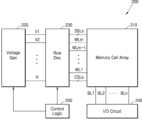
도 1은 일 실시예에 따른 메모리 시스템을 나타내는 블록도이다.
도 2는 도 1에 도시된 메모리 장치의 일 구현예를 나타내는 블록도이다.
도 3은 도 1에 도시된 메모리 셀 어레이를 보이는 블록도이다.
도 4는 일 실시예에 따른 메모리 블록에 대응하는 등가 회로를 나타내는 도면이다.
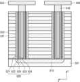
도 5는 일 실시예에 따른 메모리 블록에 대응하는 물리적 구조를 개략적으로 보이는 사시도이다.
도 6a는 도 5에 도시된 메모리 블록의 XZ평면의 단면을 보이는 단면도이다.
도 6b는 도 5에 도시된 메모리 블록의 YZ평면의 단면을 보이는 단면도이다.
도 7은 일 실시예에 따른 비휘발성 메모리 장치의 프로그램 모드시 도 4에 따른 메모리 블록의 등가 회로를 나타내는 도면이다.
도 8은 일 실시예에 따른 프로그램 모드시 유전체막과 저항 변화층에서 전류 이동을 개략적으로 설명하기 위한 도면이다.
도 9는 일 실시예에 따른 메모리 블록의 독출 모드시의 회로를 나타내는 도면이다.
도 10은 일 실시예에 따른 독출 모드시 선택 메모리 셀에서 전류 이동을 설명하기 위한 도면이다.
도 11은 일 실시예에 따른 메모리 셀의 동작을 실험하기 위하여 고안된 구조를 보이는 TEM(transmission electron microscope) 사진이다.
도 12는 도 11에 도시된 구조에서 저항 변화 유도를 위한 동작 조건에서 전계 분포를 시뮬레이션한 결과를 보인다.
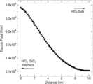
도 13은 도 11에 도시된 구조에서 수평 방향의 거리에 따른 전계의 세기 변화를 보이는 그래프이다.
도 14 및 도 15는 도 11에 도시된 구조의 저항 변화 특성을 예시적으로 보이는 그래프이다.
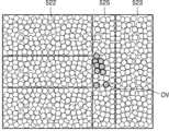
도 16a 및 도 16b는 메모리 셀의 유전체막 내부에서 저항 변화 동작에 따른 산소 공공의 이동을 예시적으로 보이는 개념도이다.
도 17은 일 실시예에 따른 메모리 셀 내의 유전체막의 구조를 개략적으로 보이는 단면도이다.FIG. 1 is a block diagram illustrating a memory system according to one embodiment.
FIG. 2 is a block diagram showing one implementation example of the memory device illustrated in FIG. 1.
FIG. 3 is a block diagram showing the memory cell array illustrated in FIG. 1.
FIG. 4 is a diagram showing an equivalent circuit corresponding to a memory block according to one embodiment.
FIG. 5 is a perspective view schematically showing a physical structure corresponding to a memory block according to one embodiment.
FIG. 6a is a cross-sectional view showing a cross-section of the XZ plane of the memory block illustrated in FIG. 5.
Fig. 6b is a cross-sectional view showing a cross-section of the YZ plane of the memory block illustrated in Fig. 5.
FIG. 7 is a diagram showing an equivalent circuit of a memory block according to FIG. 4 in a program mode of a nonvolatile memory device according to one embodiment.
FIG. 8 is a drawing schematically explaining current movement in a dielectric film and a resistance change layer in a program mode according to one embodiment.
FIG. 9 is a diagram showing a circuit in read mode of a memory block according to one embodiment.
FIG. 10 is a diagram for explaining current movement in a selected memory cell in read mode according to one embodiment.
FIG. 11 is a transmission electron microscope (TEM) photograph showing a structure designed to experiment with the operation of a memory cell according to one embodiment.
Figure 12 shows the results of simulating the electric field distribution under operating conditions for inducing resistance change in the structure illustrated in Figure 11.
Figure 13 is a graph showing the change in electric field intensity according to horizontal distance in the structure illustrated in Figure 11.
Figures 14 and 15 are graphs exemplarily showing the resistance change characteristics of the structure illustrated in Figure 11.
Figures 16a and 16b are conceptual diagrams exemplifying the movement of oxygen vacancies according to the resistance change operation within the dielectric film of a memory cell.
FIG. 17 is a cross-sectional view schematically showing the structure of a dielectric film in a memory cell according to one embodiment.
이하, 첨부된 도면들을 참조하여, 메모리 셀 스트링을 포함하는 수직형 비휘발성 메모리 장치에 대해 상세하게 설명한다. 이하의 도면들에서 동일한 참조부호는 동일한 구성요소를 지칭하며, 도면상에서 각 구성요소의 크기는 설명의 명료성과 편의상 과장되어 있을 수 있다. 또한, 이하에 설명되는 실시예는 단지 예시적인 것에 불과하며, 이러한 실시예들로부터 다양한 변형이 가능하다.Hereinafter, with reference to the attached drawings, a vertical nonvolatile memory device including a memory cell string will be described in detail. In the drawings below, the same reference numerals refer to the same components, and the size of each component in the drawings may be exaggerated for clarity and convenience of explanation. In addition, the embodiments described below are merely exemplary, and various modifications are possible from these embodiments.
이하에서, "상부" 나 "상"이라고 기재된 것은 접촉하여 바로 위에 있는 것뿐만 아니라 비접촉으로 위에 있는 것도 포함할 수 있다. 단수의 표현은 문맥상 명백하게 다르게 뜻하지 않는 한, 복수의 표현을 포함한다. 또한 어떤 부분이 어떤 구성요소를 "포함"한다고 할 때, 이는 특별히 반대되는 기재가 없는 한 다른 구성요소를 제외하는 것이 아니라 다른 구성요소를 더 포함할 수 있는 것을 의미한다.Hereinafter, the expression "upper" or "upper" may include not only what is directly above in contact, but also what is above in a non-contact manner. The singular expression includes the plural expression unless the context clearly indicates otherwise. Also, when a part is said to "include" a certain component, this does not mean that it excludes other components, but rather that it may include other components, unless otherwise specifically stated.
"상기"의 용어 및 이와 유사한 지시 용어의 사용은 단수 및 다수 모두에 해당하는 것일 수 있다. 방법을 구성하는 단계들에 대하여 명백하게 순서를 기재하거나 반하는 기재가 없다면, 이러한 단계들은 적당한 순서로 행해질 수 있으며, 반드시 기재된 순서에 한정되는 것은 아니다.The use of the term "above" and similar referential terms may refer to both the singular and the plural. Unless the steps of a method are explicitly stated to be in a particular order or to the contrary, these steps may be performed in any suitable order, and are not necessarily limited to the order stated.
또한, 명세서에 기재된 "...부", "모듈" 등의 용어는 적어도 하나의 기능이나 동작을 처리하는 단위를 의미하며, 이는 하드웨어 또는 소프트웨어로 구현되거나 하드웨어와 소프트웨어의 결합으로 구현될 수 있다.Additionally, terms such as "part", "module", etc. described in the specification mean a unit that processes at least one function or operation, which may be implemented by hardware or software, or a combination of hardware and software.
도면에 도시된 구성 요소들 간의 선들의 연결 또는 연결 부재들은 기능적인 연결 및/또는 물리적 또는 회로적 연결들을 예시적으로 나타낸 것으로서, 실제 장치에서는 대체 가능하거나 추가의 다양한 기능적인 연결, 물리적인 연결, 또는 회로 연결들로서 나타내어질 수 있다.The connections or lack of connections between the lines depicted in the drawings are merely illustrative of functional connections and/or physical or circuit connections, and may be represented in an actual device as alternative or additional various functional connections, physical connections, or circuit connections.
모든 예들 또는 예시적인 용어의 사용은 단순히 기술적 사상을 상세히 설명하기 위한 것으로서 청구범위에 의해 한정되지 않는 이상 이런 예들 또는 예시적인 용어로 인해 범위가 한정되는 것은 아니다.Any use of examples or exemplary terms is merely intended to elaborate technical ideas and is not intended to limit the scope of the invention unless otherwise defined by the claims.
도 1은 일 실시예에 따른 메모리 시스템을 나타내는 블록도이다. 도 1을 참조하면, 일 실시예에 따른 메모리 시스템(10)은 메모리 콘트롤러(100) 및 메모리 장치(200)를 포함할 수 있다. 메모리 콘트롤러(100)는 메모리 장치(200)에 대한 제어 동작을 수행하며, 일 예로서 메모리 콘트롤러(100)는 메모리 장치(200)에 어드레스(ADD) 및 커맨드(CMD)를 제공함으로써, 메모리 장치(200)에 대한 프로그램(program)(또는 기입), 독출(read) 및 소거(erase) 동작을 수행할 수 있다. 또한, 프로그램 동작을 위한 데이터와 독출된 데이터가 메모리 콘트롤러(100)와 메모리 장치(200) 사이에서 송수신될 수 있다.FIG. 1 is a block diagram illustrating a memory system according to one embodiment. Referring to FIG. 1, a memory system (10) according to one embodiment may include a memory controller (100) and a memory device (200). The memory controller (100) performs a control operation for the memory device (200), and as an example, the memory controller (100) may perform a program (or write), read, and erase operation for the memory device (200) by providing an address (ADD) and a command (CMD) to the memory device (200). In addition, data for the program operation and read data may be transmitted and received between the memory controller (100) and the memory device (200).
메모리 장치(200)는 메모리 셀 어레이(210) 및 전압 발생부(220)를 포함할 수 있다. 메모리 셀 어레이(210)는 복수의 워드 라인과 복수의 비트 라인이 교차하는 영역들에 배치되는 복수의 메모리 셀을 포함할 수 있다. 메모리 셀 어레이(210)는 데이터를 비휘발성하게 저장하는 비휘발성 메모리 셀들을 포함할 수 있으며, 비휘발성 메모리 셀들로서, 메모리 셀 어레이(210)는 낸드(NAND) 플래시 메모리 셀 어레이(210) 또는 노어(NOR) 플래시 메모리 셀 어레이(210) 등의 플래시 메모리 셀들을 포함할 수 있다. 이하에서는, 메모리 셀 어레이(210)가 플래시 메모리 셀 어레이(210)를 포함하고, 이에 따라 메모리 장치(200)가 비휘발성 메모리 장치임을 가정하여 본 개시의 실시예들을 상술하기로 한다.The memory device (200) may include a memory cell array (210) and a voltage generator (220). The memory cell array (210) may include a plurality of memory cells arranged in areas where a plurality of word lines and a plurality of bit lines intersect. The memory cell array (210) may include nonvolatile memory cells that nonvolatilely store data, and as nonvolatile memory cells, the memory cell array (210) may include flash memory cells such as a NAND flash memory cell array (210) or a NOR flash memory cell array (210). Hereinafter, embodiments of the present disclosure will be described in detail assuming that the memory cell array (210) includes a flash memory cell array (210) and thus the memory device (200) is a nonvolatile memory device.
메모리 콘트롤러(100)는 기록/독출 제어부(110), 전압 제어부(120) 및 데이터 판별부(130)를 포함할 수 있다.The memory controller (100) may include a write/read control unit (110), a voltage control unit (120), and a data determination unit (130).
기록/독출 제어부(110)는 메모리 셀 어레이(210)에 대한 프로그램/독출 및 소거 동작을 수행하기 위한 어드레스(ADD) 및 커맨드(CMD)를 생성할 수 있다. 또한, 전압 제어부(120)는 비휘발성 메모리 장치(200) 내에서 이용되는 적어도 하나의 전압 레벨을 제어하기 전압 제어신호를 생성할 수 있다. 예를 들어, 전압 제어부(120)는 메모리 셀 어레이(210)로부터 데이터를 독출하거나, 메모리 셀 어레이(210)에 데이터를 프로그램하기 위한 워드 라인의 전압 레벨을 제어하기 위한 전압 제어신호를 생성할 수 있다.The write/read control unit (110) can generate an address (ADD) and a command (CMD) for performing a program/read and erase operation for the memory cell array (210). In addition, the voltage control unit (120) can generate a voltage control signal for controlling at least one voltage level used in the nonvolatile memory device (200). For example, the voltage control unit (120) can generate a voltage control signal for controlling a voltage level of a word line for reading data from the memory cell array (210) or programming data into the memory cell array (210).
데이터 판별부(130)는 메모리 장치(200)로부터 독출된 데이터에 대한 판별 동작을 수행할 수 있다. 예컨대, 메모리 셀들로부터 독출된 데이터를 판별하여, 상기 메모리 셀들 중 온 셀(on cell) 및/또는 오프 셀(off cell)의 개수를 판별할 수 있다. 일 동작예로서, 복수의 메모리 셀들에 대해 프로그램이 수행되면, 소정의 독출 전압을 이용하여 상기 메모리 셀들의 데이터의 상태를 판별함으로써, 모든 셀들에 대해 정상적으로 프로그램이 완료되었는지가 판별될 수 있다.The data determination unit (130) can perform a determination operation on data read out from the memory device (200). For example, by determining data read out from memory cells, the number of on cells and/or off cells among the memory cells can be determined. As an example of an operation, when a program is performed on a plurality of memory cells, by determining the state of the data of the memory cells using a predetermined read voltage, it can be determined whether the program has been completed normally for all cells.
메모리 장치(200)는 메모리 셀 어레이(210) 및 전압 발생부(220)를 포함할 수 있다. 전술한 바와 같이 메모리 셀 어레이(210)는 비휘발성 메모리 셀들을 포함할 수 있으며, 예를 들어, 메모리 셀 어레이(210)는 플래시 메모리 셀들을 포함할 수 있다. 또한, 플래시 메모리 셀들은 다양한 형태로 구현될 수 있으며, 예컨대 메모리 셀 어레이(210)는 3차원(또는 수직형, Vertical) NAND(VNAND) 메모리 셀들을 포함할 수 있다.The memory device (200) may include a memory cell array (210) and a voltage generator (220). As described above, the memory cell array (210) may include nonvolatile memory cells, for example, the memory cell array (210) may include flash memory cells. In addition, the flash memory cells may be implemented in various forms, for example, the memory cell array (210) may include three-dimensional (or vertical) NAND (VNAND) memory cells.
도 2는 도 1에 도시된 메모리 장치(200)의 일 구현예를 나타내는 블록도이다. 도 2를 참조하면, 메모리 장치(200)는 로우 디코더(230), 입출력 회로(240), 및 제어 로직(250)을 더 포함할 수 있다.FIG. 2 is a block diagram showing an implementation example of the memory device (200) illustrated in FIG. 1. Referring to FIG. 2, the memory device (200) may further include a row decoder (230), an input/output circuit (240), and control logic (250).
메모리 셀 어레이(210)는 하나 이상의 스트링 선택 라인(SSL), 복수의 워드 라인(WL1~WLm) 및 하나 이상의 공통 소스 라인(CSLs)에 연결될 수 있으며, 또한 복수의 비트 라인(BL1~BLn)에 연결될 수 있다. 전압 발생부(220)는 하나 이상의 워드 라인 전압(V1~Vi)을 발생시킬 수 있으며, 상기 워드 라인 전압(V1~Vi)들은 로우 디코더(230)로 제공될 수 있다. 비트 라인(BL1~BLn)들을 통해 프로그램/독출/소거 동작을 위한 신호가 메모리 셀 어레이(210)에 인가될 수 있다.A memory cell array (210) can be connected to one or more string select lines (SSLs), a plurality of word lines (WL1 to WLm), and one or more common source lines (CSLs), and can also be connected to a plurality of bit lines (BL1 to BLn). A voltage generator (220) can generate one or more word line voltages (V1 to Vi), and the word line voltages (V1 to Vi) can be provided to a row decoder (230). Signals for program/read/erase operations can be applied to the memory cell array (210) through the bit lines (BL1 to BLn).
또한, 프로그램될 데이터는 입출력 회로(240)를 통해 메모리 셀 어레이(210)에 제공될 수 있으며, 독출된 데이터는 입출력 회로(240)를 통해 외부(예를 들어, 메모리 컨트롤러)에 제공될 수 있다. 제어 로직(250)은 메모리 동작과 관련된 각종 제어 신호들을 로우 디코더(230) 및 전압 발생부(220)에 제공할 수 있다.In addition, data to be programmed can be provided to the memory cell array (210) through the input/output circuit (240), and read data can be provided to the outside (e.g., a memory controller) through the input/output circuit (240). The control logic (250) can provide various control signals related to memory operation to the row decoder (230) and the voltage generator (220).
로우 디코더(230)의 디코딩 동작에 따라, 워드 라인 전압(V1~Vi)들은 각종 라인(SSLs, WL1~WLm, CSLs)들에 제공될 수 있다. 예컨대, 워드 라인 전압(V1~Vi)들은 스트링 선택 전압, 워드 라인 전압 및 접지 선택 전압들을 포함할 수 있으며, 스트링 선택 전압은 하나 이상의 스트링 선택 라인(SSLs)에 제공되고, 워드 라인 전압은 하나 이상의 워드 라인(WL1~WLm)에 제공되며, 접지 선택 전압은 하나 이상의 공통 소스 라인(CSLs)에 제공될 수 있다.According to the decoding operation of the row decoder (230), the word line voltages (V1 to Vi) may be provided to various lines (SSLs, WL1 to WLm, CSLs). For example, the word line voltages (V1 to Vi) may include string selection voltages, word line voltages, and ground selection voltages, and the string selection voltage may be provided to one or more string selection lines (SSLs), the word line voltage may be provided to one or more word lines (WL1 to WLm), and the ground selection voltage may be provided to one or more common source lines (CSLs).
도 3은 도 1에 도시된 메모리 셀 어레이를 보이는 블록도이다. 도 3을 참조하면, 메모리 셀 어레이(210)는 복수의 메모리 블록(BLK1~BLKz)을 포함한다. 각각의 메모리 블록(BLK)은 3차원 구조(또는 수직 구조)를 갖는다. 예를 들어, 각각의 메모리 블록(BLK)은 제 1 내지 제 3 방향들을 따라 연장된 구조물들을 포함할 수 있다. 예를 들면, 각각의 메모리 블록(BLK)은 제 2 방향을 따라 연장된 복수의 메모리 셀 스트링을 포함할 수 있다. 또한, 복수의 메모리 셀 스트링은 제 1 및 제 3 방향들을 따라 2차원 배열될 수 있다. 각각의 메모리 셀 스트링은 비트 라인(BL), 스트링 선택 라인(SSL), 워드 라인들(WL), 및 공통 소스 라인(CSL)에 연결된다. 따라서, 각각의 메모리 블록(BLK1~BLKz)은 복수의 비트 라인(BL), 복수의 스트링 선택 라인(SSLs). 복수의 워드 라인(WL), 그리고 복수의 공통 소스 라인(CSL)에 연결될 것이다. 이러한 메모리 블록(BLK1~BLKz)들은 도 4를 참조하여 더 상세하게 설명된다.FIG. 3 is a block diagram showing the memory cell array illustrated in FIG. 1. Referring to FIG. 3, the memory cell array (210) includes a plurality of memory blocks (BLK1 to BLKz). Each memory block (BLK) has a three-dimensional structure (or a vertical structure). For example, each memory block (BLK) may include structures extending along first to third directions. For example, each memory block (BLK) may include a plurality of memory cell strings extending along a second direction. In addition, the plurality of memory cell strings may be two-dimensionally arranged along the first and third directions. Each memory cell string is connected to a bit line (BL), a string select line (SSL), word lines (WL), and a common source line (CSL). Therefore, each memory block (BLK1 to BLKz) includes a plurality of bit lines (BL), a plurality of string select lines (SSLs). will be connected to multiple word lines (WL) and multiple common source lines (CSL). These memory blocks (BLK1 to BLKz) are described in more detail with reference to Fig. 4.
도 4는 일 실시예에 따른 메모리 블록에 대응하는 등가 회로를 나타내는 도면이다. 예시적으로, 도 3의 메모리 셀 어레이(210)의 메모리 블록(BLK1~BLKz)들 중 하나가 도 4에 도시된다. 도 3 및 도 4를 참조하면, 메모리 블록(BLK1~BLKz)은 각각 복수의 메모리 셀 스트링(CS11~CSkn)을 포함한다. 복수의 메모리 셀 스트링(CS11~CSkn)은 행 방향 및 열 방향을 따라 2차원 배열되어 행들 및 열들을 형성할 수 있다. 각각의 메모리 셀 스트링(CS11~CSkn)은 복수의 메모리 셀(MC) 및 복수의 스트링 선택 트랜지스터(SST)를 포함한다. 각각의 메모리 셀 스트링(CS11~CSkn)의 메모리 셀(MC)들 및 스트링 선택 트랜지스터(SST)들은 높이 방향으로 적층될 수 있다.FIG. 4 is a diagram showing an equivalent circuit corresponding to a memory block according to one embodiment. For example, one of the memory blocks (BLK1 to BLKz) of the memory cell array (210) of FIG. 3 is illustrated in FIG. 4. Referring to FIGS. 3 and 4, the memory blocks (BLK1 to BLKz) each include a plurality of memory cell strings (CS11 to CSkn). The plurality of memory cell strings (CS11 to CSkn) may be two-dimensionally arranged along the row direction and the column direction to form rows and columns. Each memory cell string (CS11 to CSkn) includes a plurality of memory cells (MC) and a plurality of string select transistors (SST). The memory cells (MC) and the string select transistors (SST) of each memory cell string (CS11 to CSkn) may be stacked in the height direction.
복수의 메모리 셀 스트링(CS11~CSkn)의 행들은 서로 다른 스트링 선택 라인들(SSL1~SSLk)에 각각 연결된다. 예를 들어, 메모리 셀 스트링(CS11~CS1n)들의 스트링 선택 트랜지스터(SST)들은 스트링 선택 라인(SSL1)에 공통으로 연결된다. 메모리 셀 스트링(CSk1~CSkn)의 스트링 선택 트랜지스터(SST)들은 스트링 선택 라인(SSLk)에 공통으로 연결된다.Rows of a plurality of memory cell strings (CS11 to CSkn) are respectively connected to different string select lines (SSL1 to SSLk). For example, string select transistors (SST) of memory cell strings (CS11 to CS1n) are commonly connected to a string select line (SSL1). String select transistors (SST) of memory cell strings (CSk1 to CSkn) are commonly connected to a string select line (SSLk).
또한, 복수의 메모리 셀 스트링(CS11~CSkn)의 열들은 서로 다른 비트 라인들(BL1~BLn)에 각각 연결된다. 예를 들어, 메모리 셀 스트링(CS11~CSk1)들의 메모리 셀(MC)들 및 스트링 선택 트랜지스터(SST)들은 비트 라인(BL1)에 공통으로 연결될 수 있으며, 메모리 셀 스트링(CS1n~CSkn)들의 메모리 셀(MC)들 및 스트링 선택 트랜지스터(SST)들은 비트 라인(BLn)에 공통으로 연결될 수 있다.In addition, the columns of the plurality of memory cell strings (CS11 to CSkn) are respectively connected to different bit lines (BL1 to BLn). For example, the memory cells (MC) and string select transistors (SST) of the memory cell strings (CS11 to CSk1) may be commonly connected to the bit line (BL1), and the memory cells (MC) and string select transistors (SST) of the memory cell strings (CS1n to CSkn) may be commonly connected to the bit line (BLn).
또한, 복수의 메모리 셀 스트링(CS11~CSkn)의 행들은 서로 다른 공통 소스 라인(CSL1~CSLk)들에 각각 연결될 수 있다. 예를 들어, 복수의 메모리 셀 스트링(CS11~CS1n)들의 스트링 선택 트랜지스터(SST)들은 공통 소스 라인(CSL1)에 공통으로 연결될 수 있으며, 복수의 메모리 셀 스트링(CSk1~CSkn)들의 스트링 선택 트랜지스터(SST)들은 공통 소스 라인(CSLk)에 공통으로 연결될 수 있다.In addition, rows of the plurality of memory cell strings (CS11 to CSkn) may be respectively connected to different common source lines (CSL1 to CSLk). For example, string select transistors (SST) of the plurality of memory cell strings (CS11 to CS1n) may be commonly connected to the common source line (CSL1), and string select transistors (SST) of the plurality of memory cell strings (CSk1 to CSkn) may be commonly connected to the common source line (CSLk).
기판(또는 스트링 선택 트랜지스터(SST)들)으로부터 동일한 높이에 위치한 메모리 셀(MC)들은 하나의 워드 라인(WL)에 공통으로 연결되고, 서로 다른 높이에 위치한 메모리 셀(MC)들은 서로 다른 워드 라인들(WL1~WLm)에 각각 연결될 수 있다.Memory cells (MC) located at the same height from the substrate (or string select transistors (SSTs)) are commonly connected to one word line (WL), and memory cells (MC) located at different heights can be connected to different word lines (WL1 to WLm), respectively.
도 4에 도시된 메모리 블록은 예시적인 것이다. 본 개시의 기술적 사상은 도 4에 도시된 메모리 블록에 한정되지 않는다. 예를 들어, 복수의 메모리 셀 스트링(CS11~CSkn)들의 행들의 수는 증가 또는 감소될 수 있다. 복수의 메모리 셀 스트링(CS11~CSkn)의 행들의 수가 변경됨에 따라, 메모리 셀 스트링(CS11~CSkn)의 행들에 연결되는 스트링 선택 라인들의 수, 그리고 하나의 비트 라인에 연결되는 메모리 셀 스트링(CS11~CSkn)의 수 또한 변경될 수 있다. 메모리 셀 스트링(CS11~CSkn)의 행들의 수가 변경됨에 따라, 메모리 셀 스트링(CS11~CSkn)의 행들에 연결되는 공통 소스 라인들의 수 또한 변경될 수 있다. 또한, 메모리 셀 스트링(CS11~CSkn)의 열들의 수가 증가 또는 감소될 수 있다. 메모리 셀 스트링(CS11~CSkn)의 열들의 수가 변경됨에 따라, 메모리 셀 스트링(CS11~CSkn)의 열들에 연결되는 비트 라인들의 수, 그리고 하나의 스트링 선택 라인에 연결되는 메모리 셀 스트링(CS11~CSkn)의 수 또한 변경될 수 있다.The memory block illustrated in FIG. 4 is exemplary. The technical idea of the present disclosure is not limited to the memory block illustrated in FIG. 4. For example, the number of rows of the plurality of memory cell strings (CS11 to CSkn) may be increased or decreased. As the number of rows of the plurality of memory cell strings (CS11 to CSkn) is changed, the number of string selection lines connected to the rows of the memory cell strings (CS11 to CSkn) and the number of memory cell strings (CS11 to CSkn) connected to one bit line may also be changed. As the number of rows of the memory cell strings (CS11 to CSkn) is changed, the number of common source lines connected to the rows of the memory cell strings (CS11 to CSkn) may also be changed. In addition, the number of columns of the memory cell strings (CS11 to CSkn) may be increased or decreased. As the number of columns of the memory cell strings (CS11 to CSkn) changes, the number of bit lines connected to the columns of the memory cell strings (CS11 to CSkn) and the number of memory cell strings (CS11 to CSkn) connected to one string select line may also change.
각각의 메모리 셀 스트링(CS11~CSkn)의 높이는 증가 또는 감소될 수 있다. 예를 들어, 각각의 메모리 셀 스트링(CS11~CSkn)에 적층되는 메모리 셀(MC)들의 수는 증가 또는 감소될 수 있다. 각각의 메모리 셀 스트링(CS11~CSkn)에 적층되는 메모리 셀(MC)들의 수가 변경됨에 따라, 워드 라인(WL)들의 수 또한 변경될 수 있다. 예를 들어, 각각의 메모리 셀 스트링(CS11~CSkn)에 제공되는 스트링 선택 트랜지스터는 증가될 수 있다. 각각의 메모리 셀 스트링(CS11~CSkn)에 제공되는 스트링 선택 트랜지스터의 수가 변경됨에 따라, 스트링 선택 라인 또는 공통 소스 라인의 수 또한 변경될 수 있다. 스트링 선택 트랜지스터의 수가 증가하면, 스트링 선택 트랜지스터들은 메모리 셀(MC)들과 같은 형태로 적층될 수 있다.The height of each memory cell string (CS11 to CSkn) may increase or decrease. For example, the number of memory cells (MC) stacked in each memory cell string (CS11 to CSkn) may increase or decrease. As the number of memory cells (MC) stacked in each memory cell string (CS11 to CSkn) changes, the number of word lines (WL) may also change. For example, the number of string select transistors provided in each memory cell string (CS11 to CSkn) may increase. As the number of string select transistors provided in each memory cell string (CS11 to CSkn) changes, the number of string select lines or common source lines may also change. When the number of string select transistors increases, the string select transistors may be stacked in the same form as the memory cells (MC).
예시적으로, 쓰기 및 독출은 메모리 셀 스트링(CS11~CSkn)들의 행의 단위로 수행될 수 있다. 공통 소스 라인들(CSLs)에 의해 메모리 셀 스트링(CS11~CSkn)들이 하나의 행들의 단위로 선택되고, 스트링 선택 라인들(SSLs)에 의해 메모리 셀 스트링(CS11~CSkn)들이 하나의 행 단위로 선택될 수 있다. 그리고, 메모리 셀 스트링(CS11~CSkn)의 선택된 행에서, 쓰기 및 독출은 페이지의 단위로 수행될 수 있다. 예를 들어, 페이지는 하나의 워드 라인(WL)에 연결된 메모리 셀(MC)들의 하나의 행일 수 있다. 메모리 셀 스트링(CS11~CSkn)의 선택된 행에서, 메모리 셀(MC)들은 워드 라인들(WL)에 의해 페이지의 단위로 선택될 수 있다.For example, writing and reading may be performed in units of rows of memory cell strings (CS11 to CSkn). The memory cell strings (CS11 to CSkn) may be selected in units of rows by common source lines (CSLs), and the memory cell strings (CS11 to CSkn) may be selected in units of rows by string select lines (SSLs). And, in the selected row of the memory cell strings (CS11 to CSkn), writing and reading may be performed in units of pages. For example, a page may be one row of memory cells (MC) connected to one word line (WL). In the selected row of the memory cell strings (CS11 to CSkn), memory cells (MC) may be selected in units of pages by the word lines (WL).
한편, 각각의 메모리 셀 스트링(CS11~CSkn) 내의 메모리 셀(MC)들은 트랜지스터와 저항이 병렬로 연결된 회로에 대응될 수 있다. 예를 들어, 도 5는 일 실시예에 따른 메모리 블록에 대응하는 물리적 구조를 개략적으로 보이는 사시도이고, 도 6a는 도 5에 도시된 메모리 블록의 XZ평면의 단면을 보이는 단면도이며, 도 6b는 도 5에 도시된 메모리 블록의 YZ평면의 단면을 보이는 단면도이Meanwhile, the memory cells (MC) in each memory cell string (CS11 to CSkn) may correspond to a circuit in which transistors and resistors are connected in parallel. For example, FIG. 5 is a perspective view schematically showing a physical structure corresponding to a memory block according to one embodiment, FIG. 6a is a cross-sectional view showing a cross-section of the XZ plane of the memory block shown in FIG. 5, and FIG. 6b is a cross-sectional view showing a cross-section of the YZ plane of the memory block shown in FIG. 5.
도 5, 도 6a, 도 6b를 참조하면, 메모리 블록은 기판(501)을 포함한다. 기판(501)은 제 1 타입 불순물로 도핑된 실리콘 물질을 포함할 수 있다. 예를 들어, 기판(501)은 p 타입 불순물로 도핑된 실리콘 물질을 포함할 수 있다. 기판(501)은, 예를 들어, p 타입 웰(예를 들면, 포켓 p 웰)일 수 있다. 이하에서, 기판(501)은 p 타입 실리콘인 것으로 가정하지만, 기판(501)은 p 타입 실리콘으로 한정되지 않는다.Referring to FIGS. 5, 6A, and 6B, the memory block includes a substrate (501). The substrate (501) may include a silicon material doped with a first type impurity. For example, the substrate (501) may include a silicon material doped with a p-type impurity. The substrate (501) may be, for example, a p-type well (e.g., a pocket p well). Hereinafter, the substrate (501) is assumed to be p-type silicon, but the substrate (501) is not limited to p-type silicon.
기판(501)의 상부 영역에는 도핑 영역(510)이 형성되어 있다. 예를 들어, 도핑 영역(510)은 기판(501)과 전기적으로 상반되는 제 2 타입을 갖는다. 예를 들어, 도핑 영역(510)은 n-타입을 갖는다. 이하에서, 도핑 영역(510)은 n-타입인 것으로 가정한다. 그러나 도핑 영역(510)은 n-타입인 것으로 한정되지 않는다. 이러한 도핑 영역(510)은 공통 소스 라인이 될 수 있다.A doped region (510) is formed in an upper region of the substrate (501). For example, the doped region (510) has a second type that is electrically opposite to that of the substrate (501). For example, the doped region (510) has an n-type. Hereinafter, the doped region (510) is assumed to be an n-type. However, the doped region (510) is not limited to being an n-type. This doped region (510) can be a common source line.
기판(501)에는 수평 방향을 따라 연장된 복수의 게이트(531) 및 수평 방향을 따라 연장된 복수의 절연체(532)가 번갈아 배열될 수 있다. 다시 말해, 복수의 게이트(531) 및 복수의 절연체(532)는 수평 방향에 직교하는 수직 방향을 따라 서로 번갈아 적층될 수 있다. 예를 들어, 게이트(531)는 금속 물질(예를 들어, 구리, 은 등) 및 고농도로 도핑된 실리콘 중 적어도 하나를 포함하고, 복수의 절연체(532)는 실리콘 산화물을 포함할 수 있으나, 이에 제한되지 않는다. 각각의 게이트(531)는 워드 라인(WL), 스트링 선택 라인(SSL) 중 하나와 연결된다.A plurality of gates (531) extending in a horizontal direction and a plurality of insulators (532) extending in a horizontal direction may be alternately arranged on the substrate (501). In other words, the plurality of gates (531) and the plurality of insulators (532) may be alternately stacked along a vertical direction orthogonal to the horizontal direction. For example, the gates (531) may include at least one of a metal material (e.g., copper, silver, etc.) and highly doped silicon, and the plurality of insulators (532) may include silicon oxide, but are not limited thereto. Each gate (531) is connected to one of a word line (WL) and a string select line (SSL).
또한, 메모리 블록은 수직 방향으로 번갈아 배열된 복수의 게이트(531) 및 복수의 절연체(532)을 수직 방향으로 관통하는 복수의 필라(520)를 포함한다. 각각의 필라(520)는 수평 방향을 따라 복수의 층으로 구성될 수 있다. 일 실시예에서, 필라(520)의 최외각층은 게이트 절연층(521)일 수 있다. 예를 들어, 게이트 절연층(521)은 실리콘 산화물(silicon oxide)을 포함할 수 있다. 게이트 절연층(521)은 복수의 게이트(531) 및 복수의 절연체(532)에 콘포말(conformal)하게 증착되어 수직 방향을 따라 연장될 수 있다.In addition, the memory block includes a plurality of gates (531) arranged alternately in the vertical direction and a plurality of pillars (520) penetrating the plurality of insulators (532) in the vertical direction. Each pillar (520) may be composed of a plurality of layers along the horizontal direction. In one embodiment, the outermost layer of the pillar (520) may be a gate insulating layer (521). For example, the gate insulating layer (521) may include silicon oxide. The gate insulating layer (521) may be conformally deposited on the plurality of gates (531) and the plurality of insulators (532) and may extend along the vertical direction.
또한, 게이트 절연층(521)의 표면을 따라 반도체층(522)이 콘포말하게 증착되어 수직 방향을 따라 연장될 수 있다. 일 실시예에서 반도체층(522)은 제 1 타입으로 도핑된 실리콘 물질을 포함할 수 있다. 반도체층(522)은 기판(501)과 동일한 타입으로 도핑된 실리콘 물질을 포함할 수 있으며, 예를 들어, 기판(501)이 p-타입으로 도핑된 실리콘 물질을 포함하는 경우, 반도체층(522) 역시 p-타입으로 도핑된 실리콘 물질을 포함할 수 있다. 또는 반도체층(522)는 Ge, IGZO(indium gallium zinc oxide), GaAs 등의 물질도 포함될 수 있다.In addition, a semiconductor layer (522) may be conformally deposited along a surface of the gate insulating layer (521) and may extend in a vertical direction. In one embodiment, the semiconductor layer (522) may include a silicon material doped with a first type. The semiconductor layer (522) may include a silicon material doped with the same type as the substrate (501), for example, when the substrate (501) includes a silicon material doped with a p-type, the semiconductor layer (522) may also include a silicon material doped with a p-type. Alternatively, the semiconductor layer (522) may also include a material such as Ge, IGZO (indium gallium zinc oxide), or GaAs.
반도체층(522)의 표면을 따라 유전체막(525)이 콘포말하게 증착되어 수직 방향을 따라 연장될 수 있다. 유전체막(525)은 반도체층(522)의 재료와 후술하는 저항 변화층(523)의 재료와의 혼합물로 이루어질 수 있다.A dielectric film (525) may be conformally deposited along the surface of the semiconductor layer (522) and may extend in the vertical direction. The dielectric film (525) may be formed of a mixture of a material of the semiconductor layer (522) and a material of the resistance change layer (523) described below.
유전체막(525)의 표면을 따라 저항 변화층(523)이 배치될 수 있다. 저항 변화층(523)은 유전체막(525)과 직접 접하게 배치될 수 있고, 유전체막(525)에 콘포말하게 증착될 수 있다. 일 실시예에서 저항 변화층(523)은 인가된 전압에 따라 저항이 달라지는 물질로 형성될 수 있다. 저항 변화층(523)은 게이트(531)에 인가된 전압에 따라 고저항 상태에서 저저항 상태 또는 저저항 상태에서 고저항 상태로 변할 수 있다. 예를 들어, 저항 변화층(523)은 전이금속 산화물을 포함할 수 있다. 구체적으로, 저항 변화층(523)은 지르코늄(Zr), 하프늄(Hf), 알루미늄(Al), 니켈(Ni), 구리(Cu), 몰리브덴(Mo), 탄탈륨(Ta), 티타늄(Ti), 텅스텐(W), 크롬(Cr), 스트론튬(Sr), 란탄(La), 망간(Mn), 칼슘(Ca), 및 프라세오디뮴(Praseodymium, Pr)을 포함하는 그룹에서 선택되는 적어도 하나의 원소의 산화물을 포함할 수 있다.A resistance change layer (523) may be arranged along a surface of a dielectric film (525). The resistance change layer (523) may be arranged in direct contact with the dielectric film (525) and may be conformally deposited on the dielectric film (525). In one embodiment, the resistance change layer (523) may be formed of a material whose resistance varies depending on an applied voltage. The resistance change layer (523) may change from a high resistance state to a low resistance state or from a low resistance state to a high resistance state depending on a voltage applied to the gate (531). For example, the resistance change layer (523) may include a transition metal oxide. Specifically, the resistance change layer (523) may include an oxide of at least one element selected from the group consisting of zirconium (Zr), hafnium (Hf), aluminum (Al), nickel (Ni), copper (Cu), molybdenum (Mo), tantalum (Ta), titanium (Ti), tungsten (W), chromium (Cr), strontium (Sr), lanthanum (La), manganese (Mn), calcium (Ca), and praseodymium (Pr).
유전체막(525)은 상술한 전이금속 산화물과 반도체층(522)의 재료와의 혼합물로 이루어질 수 있다. 예를 들어, 반도체층(522)이 실리콘(Si)으로 이루어지고 저항 변화층(523)이 HfO2으로 이루어지는 경우에, 유전체막(525)은 하프늄 실리케이트(Hf silicate, HfSixOy)로 이루어질 수 있다. 또 다른 예로서, 반도체층(522)이 게르마늄(Ge)으로 이루어지고 저항 변화층(523)이 Al2O3으로 이루어지는 경우에, 유전체막(525)은 AlGexOy로 이루어질 수 있다. 여기서, x와 y는 유전체막(525) 내에서 반도체층(522)의 재료와 저항 변화층(523)의 재료와의 비율에 따라 달라질 수 있다. 이 외에도 매우 다양한 혼합물이 유전체막(525)으로 사용될 수 있다.The dielectric film (525) may be formed of a mixture of the above-described transition metal oxide and the material of the semiconductor layer (522). For example, when the semiconductor layer (522) is formed of silicon (Si) and the resistance switching layer (523) is formed of HfO2 , the dielectric film (525) may be formed of hafnium silicate (HfSix Oy ). As another example, when the semiconductor layer (522) is formed of germanium (Ge) and the resistance switching layer (523) is formed of Al2 O3 , the dielectric film (525) may be formed of AlGex Oy . Here, x and y may vary depending on the ratio of the material of the semiconductor layer (522) and the material of the resistance switching layer (523) within the dielectric film (525). In addition, a wide variety of mixtures may be used as the dielectric film (525).
유전체막(525)은 게이트(531)에 인가된 전압에 따라 저항 변화층(523)과 함께 고저항 상태에서 저저항 상태 또는 저저항 상태에서 고저항 상태로 변할 수 있다. 특히, 유전체막(525) 내에는 이동 가능한 복수의 산소 공공(oxygen vacancy)이 분포되어 있어서, 산소 공공에 의해 형성된 트랩에 전자가 트랩/디트랩되는 현상에 의해 유전체막(525)의 저항 상태가 쉽게 변화할 수 있다. 따라서, 유전체막(525)이 실질적으로 저항의 변화를 제공하는 역할을 하는 것이고, 저항 변화층(523)은 유전체막(525)에 저항 변화 물질을 제공하는 역할을 할 수 있다.The dielectric film (525) can change from a high resistance state to a low resistance state or from a low resistance state to a high resistance state together with the resistance change layer (523) depending on the voltage applied to the gate (531). In particular, since a plurality of movable oxygen vacancies are distributed within the dielectric film (525), the resistance state of the dielectric film (525) can easily change by a phenomenon in which electrons are trapped/detrapped in traps formed by the oxygen vacancies. Therefore, the dielectric film (525) actually plays a role of providing a change in resistance, and the resistance change layer (523) can play a role of providing a resistance change material to the dielectric film (525).
유전체막(525)의 내부에 충분한 양의 산소 공공이 발생할 수 있도록, 유전체막(525) 내의 반도체층(522)의 재료의 비율이 적절히 선택될 수 있다. 예를 들어, 유전체막(525) 내에서 반도체층(522)의 재료의 비율은, 사용된 전이금속 산화물과 반도체 재료에 따라 달라질 수 있지만, 약 20 at.% 내지 약 80 at.%일 수 있다. 또는, 유전체막(525) 내에서 반도체층(522)의 재료의 비율은, 예컨대, 약 40 at.% 내지 약 60 at.%일 수 있다.In order to allow a sufficient amount of oxygen vacancies to be generated inside the dielectric film (525), the ratio of the material of the semiconductor layer (522) within the dielectric film (525) may be appropriately selected. For example, the ratio of the material of the semiconductor layer (522) within the dielectric film (525) may vary depending on the transition metal oxide and semiconductor material used, but may be about 20 at.% to about 80 at.%. Alternatively, the ratio of the material of the semiconductor layer (522) within the dielectric film (525) may be, for example, about 40 at.% to about 60 at.%.
메모리 블록을 형성하는 과정에서, 반도체층(522)과 저항 변화층(523) 사이의 계면에 반도체층(522)의 재료와 저항 변화층(523)의 재료와의 혼합물로 이루어진 혼합물 박막이 자연적으로 발생할 수도 있다. 그러나, 자연적으로 발생한 혼합물 박막은 균일한 조성을 갖지 못한다. 개시된 실시예에서는 반도체층(522)과 저항 변화층(523) 사이에 의도적으로 유전체막(525)을 형성한다. 이렇게 의도적으로 형성된 유전체막(525)은 유전체막(525)의 전체 영역에 걸쳐 비교적 균일한 조성을 가질 수 있다. 예를 들어, 유전체막(525) 내의 반도체층(522)의 재료의 비율은 유전체막(525)의 전체 영역에서 약 10 %의 편차 범위 내에서 일정하게 유지될 수 있다.In the process of forming a memory block, a mixture thin film composed of a mixture of a material of the semiconductor layer (522) and a material of the resistance change layer (523) may naturally occur at the interface between the semiconductor layer (522) and the resistance change layer (523). However, the naturally occurring mixture thin film does not have a uniform composition. In the disclosed embodiment, a dielectric film (525) is intentionally formed between the semiconductor layer (522) and the resistance change layer (523). The dielectric film (525) thus intentionally formed may have a relatively uniform composition over the entire area of the dielectric film (525). For example, the ratio of the material of the semiconductor layer (522) within the dielectric film (525) may be constantly maintained within a deviation range of about 10% over the entire area of the dielectric film (525).
또한, 유전체막(525)의 폭은 수평 방향으로 산소 공공이 이동할 수 있는 거리를 확보하도록 선택될 수 있다. 예를 들어, 수평 방향으로 유전체막(525)의 폭은 약 1.5 nm 내지 약 10 nm의 범위 내에서 선택될 수 있다. 반도체층(522)의 재료와 저항 변화층(523)의 재료 사이에서 자연적으로 발생한 혼합물 박막은 균일한 폭을 갖지 못한다. 반면, 의도적으로 형성된 유전체막(525)은 유전체막(525)의 전체 영역에 걸쳐 비교적 균일한 폭을 가질 수 있다. 예를 들어, 유전체막(525)의 폭은 유전체막(525)의 전체 영역에서 약 10 %의 편차 범위 내에서 일정하게 유지될 수 있다.In addition, the width of the dielectric film (525) may be selected to secure a distance for oxygen vacancies to move in the horizontal direction. For example, the width of the dielectric film (525) in the horizontal direction may be selected within a range of about 1.5 nm to about 10 nm. A naturally occurring mixture thin film between the material of the semiconductor layer (522) and the material of the resistance switching layer (523) does not have a uniform width. On the other hand, an intentionally formed dielectric film (525) may have a relatively uniform width over the entire area of the dielectric film (525). For example, the width of the dielectric film (525) may be maintained constant within a deviation range of about 10% over the entire area of the dielectric film (525).
저항 변화층(523)의 내측에는 절연성 지지체(524)가 배치될 수 있다. 예를 들면, 절연성 지지체(524)는 실리콘 산화물(silicon oxide)을 포함할 수 있다. 하나의 절연성 지지체(524)와 그 절연성 지지체(524)의 외측으로 순차적으로 배치된 저항 변화층(523), 유전체막(525), 반도체층(522), 게이트 절연층(521), 복수의 게이트(531), 및 복수의 절연체(532)는 하나의 메모리 셀 스트링(CS)을 구성한다. 따라서, 절연층 지지체(524)가 메모리 셀 스트링(CS)의 가장 중심부에 배치된다. 반도체층(522), 및 반도체층(522)의 내측 표면에 차례로 배치된 유전체막(525)와 저항 변화층(523)은 도핑 영역(510), 즉 공통 소스 영역과 접하여 전기적으로 연결될 수 있다. 반도체층(522)의 외측 표면에 배치된 게이트(531)와 절연체(532)는 도핑 영역(510)과 접하지 않을 수 있다.An insulating support (524) may be arranged on the inner side of the resistance change layer (523). For example, the insulating support (524) may include silicon oxide. One insulating support (524) and the resistance change layer (523), the dielectric film (525), the semiconductor layer (522), the gate insulating layer (521), the plurality of gates (531), and the plurality of insulators (532) sequentially arranged on the outer side of the insulating support (524) constitute one memory cell string (CS). Therefore, the insulating layer support (524) is arranged at the very center of the memory cell string (CS). The semiconductor layer (522), and the dielectric film (525) and the resistance change layer (523) sequentially arranged on the inner surface of the semiconductor layer (522) may be electrically connected to the doped region (510), i.e., the common source region. The gate (531) and insulator (532) arranged on the outer surface of the semiconductor layer (522) may not be in contact with the doping region (510).
필라(520) 상에 드레인(540)이 배치될 수 있다. 드레인(540)은 제 2 타입으로 도핑된 실리콘 물질을 포함할 수 있다. 예를 들면, 드레인(540)은 n 타입으로 도핑된 실리콘 물질을 포함할 수 있다. 드레인(540) 상에, 비트 라인(550)이 배치될 수 있다. 드레인(540) 및 비트 라인(550)은 콘택 플러그들(contact plug)을 통해 연결될 수 있다. 비트 라인(550)은 금속 물질을 포함할 수 있으며, 예를 들어, 비트 라인(550)은 폴리 실리콘을 포함할 수 있다. 도전 물질은 비트 라인일 수 있다.A drain (540) may be arranged on the pillar (520). The drain (540) may include a silicon material doped with a second type. For example, the drain (540) may include a silicon material doped with an n type. A bit line (550) may be arranged on the drain (540). The drain (540) and the bit line (550) may be connected through contact plugs. The bit line (550) may include a metal material, for example, the bit line (550) may include polysilicon. The conductive material may be a bit line.
한편, 도 4와 비교하여 설명하면, 복수의 게이트(531), 복수의 절연체(532), 게이트 절연층(521), 반도체층(522), 유전체막(525) 및 저항 변화층(523)은 메모리 셀 스트링(CS)의 구성요소이다. 구체적으로, 게이트(531), 게이트 절연층(521) 및 반도체층(522)은 트랜지스터의 일 구성요소가 되고, 저항 변화층(523)과 유전체막(525)은 저항이 될 수 있다. 그리고, 어느 하나의 게이트(531), 및 상기 하나의 게이트(531)에 대해 수평 방향으로 인접하는 게이트 절연층(521)의 일부분, 반도체층(522)의 일부분, 유전체막(525)의 일부분 및 저항 변화층(523)의 일부분은 하나의 메모리 셀(MC)의 구성요소이다. 이러한 복수의 메모리 셀(MC)이 수직 적층 구조로 배열되어 각각의 메모리 셀 스트링(CS)을 형성한다.Meanwhile, compared to FIG. 4, a plurality of gates (531), a plurality of insulators (532), a gate insulating layer (521), a semiconductor layer (522), a dielectric film (525), and a resistance change layer (523) are components of a memory cell string (CS). Specifically, the gate (531), the gate insulating layer (521), and the semiconductor layer (522) become components of a transistor, and the resistance change layer (523) and the dielectric film (525) can become resistors. In addition, one gate (531), and a portion of the gate insulating layer (521), a portion of the semiconductor layer (522), a portion of the dielectric film (525), and a portion of the resistance change layer (523) horizontally adjacent to one gate (531) are components of one memory cell (MC). These plurality of memory cells (MC) are arranged in a vertically stacked structure to form each memory cell string (CS).
유전체막(525)과 저항 변화층(523)은 고저항 또는 저저항 상태를 가질 수 있어, 메모리 셀(MC)에 '0'과 '1'이 기록될 수 있다. 각 메모리 셀(MC)에서 트랜지스터의 반도체층(522)은 유전체막(525)과 저항 변화층(523)에 병렬 연결되어 있으며, 이러한 병렬 구조가 수직방향으로 연속적으로 배열됨으로서 메모리 셀 스트링(CS)이 구성될 수 있다. 그리고, 메모리 셀 스트링(CS)의 양단에 각각 공통 소스 라인(510)과 비트 라인(550)이 연결될 수 있다. 그리고, 공통 소스 라인(510)과 비트 라인(550)에 전압을 인가됨으로써 복수의 메모리 셀(MC)에 프로그램, 독출, 소거 과정이 이루어질 수 있다.The dielectric film (525) and the resistance change layer (523) can have a high resistance or low resistance state, so that '0' and '1' can be recorded in the memory cell (MC). In each memory cell (MC), the semiconductor layer (522) of the transistor is connected in parallel to the dielectric film (525) and the resistance change layer (523), and a memory cell string (CS) can be configured by arranging these parallel structures vertically and continuously. In addition, a common source line (510) and a bit line (550) can be connected to each of both ends of the memory cell string (CS). In addition, by applying voltage to the common source line (510) and the bit line (550), a program, read, and erase process can be performed on a plurality of memory cells (MC).
본 실시예에 따르면, 상변화(phase change) 물질을 이용하여 메모리 블록을 구성하는 대신 저항 변화층(523)을 이용하여 메모리 블록을 구성함으로써, 상변화 물질을 이용함에 따른 열발생, 응력(압력) 문제 등을 개선할 수 있다. 또한, 상술한 바와 같이 메모리 블록을 구성하고, 메모리 블록을 동작시킴으로써, 메모리 블록에 포함된 메모리 셀들을 반복하여 동작시키는 경우에도 인접 메모리 셀 간의 이온(ion) 이동 및 그에 따른 누설 전류, 동작 실패를 방지할 수 있다. 또한, 본 실시예에 따른 메모리 블록은 차세대 VNAND(vertical NAND)에서의 메모리 셀 간의 스케일링 이슈(scaling issue)를 해결할 수 있어 집적도(density)를 비약적으로 증가시킬 수 있다. 따라서, 메모리 용량이 크게 증가할 수 있다. 특히, 반도체층(522)과 저항 변화층(523) 사이에 산소 공공들이 이동할 수 있는 유전체막(525)을 배치함으로써 저항 상태를 보다 용이하고 정확하게 변화할 수 있다.According to the present embodiment, by configuring a memory block using a resistance change layer (523) instead of using a phase change material, problems such as heat generation and stress (pressure) due to using a phase change material can be improved. In addition, by configuring a memory block as described above and operating the memory block, even when memory cells included in the memory block are repeatedly operated, ion movement between adjacent memory cells and leakage current and operation failure resulting therefrom can be prevented. In addition, the memory block according to the present embodiment can solve a scaling issue between memory cells in the next-generation VNAND (vertical NAND), so that the density can be dramatically increased. Accordingly, the memory capacity can be significantly increased. In particular, by arranging a dielectric film (525) through which oxygen vacancies can move between the semiconductor layer (522) and the resistance change layer (523), the resistance state can be changed more easily and accurately.
한편, 본 실시예에 따른 메모리 블록은 칩 형태로 구현되어 뉴로모픽 컴퓨팅 (Neuromorphic Computing) 플랫폼으로 사용될 수 있다. 또한, 본 개시에 따른 블록은 chip 형태로 구현되어 뉴럴 네트워크(Neural Network)를 구성하는데 이용될 수 있다.Meanwhile, the memory block according to the present embodiment may be implemented in a chip form and used as a neuromorphic computing platform. In addition, the block according to the present disclosure may be implemented in a chip form and used to configure a neural network.
도 7은 일 실시예에 따른 비휘발성 메모리 장치의 프로그램 모드시 도 4에 따른 메모리 블록의 등가 회로를 나타내는 도면이다. 도 7에 표시된 복수의 메모리 셀(710, 720)은 도 5에 도시된 게이트(531), 게이트 절연층(521), 반도체층(522), 유전체막(525), 및 저항 변화층(523)을 각각 포함할 수 있다.FIG. 7 is a diagram showing an equivalent circuit of a memory block according to FIG. 4 in a program mode of a nonvolatile memory device according to one embodiment. The plurality of memory cells (710, 720) shown in FIG. 7 may each include a gate (531), a gate insulating layer (521), a semiconductor layer (522), a dielectric film (525), and a resistance change layer (523) shown in FIG. 5.
메모리 블록의 복수의 메모리 셀(710, 720)은 선택 메모리 셀(710)과 비선택 메모리 셀(720)로 구분될 수 있다. 비휘발성 장치의 프로그램 모드는 메모리 블록에 포함된 메모리 셀에 프로그램 동작을 수행하는 모드를 의미하고, 선택 메모리 셀(710)은 프로그램 동작의 대상이 되는 메모리 셀을 의미할 수 있다.A plurality of memory cells (710, 720) of a memory block can be divided into selected memory cells (710) and non-selected memory cells (720). The program mode of a non-volatile device means a mode in which a program operation is performed on a memory cell included in a memory block, and the selected memory cell (710) can mean a memory cell that is a target of the program operation.
제어 로직(250)은 복수의 스트링 선택 라인(SSLs) 중에서, 선택 메모리 셀(710)과 연결된 스트링 선택 라인(SSL)에 턴-온 전압(Von)을 인가하도록 제어할 수 있다. 제어 로직(250)은 복수의 워드 라인(WL) 중에서 비선택 메모리 셀(720)들과 연결된 워드 라인(WL)에 턴-온 전압(Von)을 인가하고, 복수의 워드 라인(WL) 중 선택 메모리 셀(710)과 연결된 워드 라인(WL)에 턴-오프 전압(Voff)을 인가할 수 있다. 여기서 턴-온 전압(Von)은 트랜지스터를 턴-온시키는 크기의 전압으로서, 트랜지스터의 반도체층에만 전류-온 시키는 전압이라고도 할 수 있다. 턴-오프 전압(Voff)은 트랜지스터를 턴-오프시키는 크기의 전압으로서, 트랜지스터의 반도체층에 전류가 흐르지 않도록 하는 전압이라고도 할 수 있다. 턴-온 전압(Von) 및 턴-오프 전압(Voff)의 크기는 복수의 메모리 셀(MC)을 형성하는 게이트(531), 게이트 절연층(521), 반도체층(522), 유전체막(525) 및 저항 변화층(523)을 구성하는 물질의 종류, 두께 등에 의해 달라질 수 있다. 일반적으로 턴-온 전압(Von)의 절대값은 턴-오프 전압(Voff)의 절대값보다 클 수 있다.The control logic (250) can control to apply a turn-on voltage (Von) to a string select line (SSL) connected to a selected memory cell (710) among a plurality of string select lines (SSLs). The control logic (250) can apply a turn-on voltage (Von) to a word line (WL) connected to unselected memory cells (720) among a plurality of word lines (WL), and can apply a turn-off voltage (Voff) to a word line (WL) connected to a selected memory cell (710) among a plurality of word lines (WL). Here, the turn-on voltage (Von) is a voltage of a magnitude that turns on the transistor, and can also be referred to as a voltage that turns on current only in the semiconductor layer of the transistor. The turn-off voltage (Voff) is a voltage of a magnitude that turns off the transistor, and can also be referred to as a voltage that prevents current from flowing in the semiconductor layer of the transistor. The magnitudes of the turn-on voltage (Von) and the turn-off voltage (Voff) may vary depending on the type and thickness of the material constituting the gate (531), the gate insulating layer (521), the semiconductor layer (522), the dielectric film (525), and the resistance change layer (523) forming a plurality of memory cells (MC). In general, the absolute value of the turn-on voltage (Von) may be greater than the absolute value of the turn-off voltage (Voff).
그리고, 복수의 비트 라인(BLs) 중 선택 메모리 셀(710)에 연결된 비트 라인(BL)에 프로그램 전압(Vprogram)이 인가될 수 있다. 프로그램 전압(Vprogram)은 입출력 회로(240)를 통해 외부, 예를 들어, 메모리 컨트롤러(100)로부터 제공될 수 있다. 프로그램 전압(Vprogram)은 메모리 셀(MC)에 데이터를 기록하기 위한 전압으로서 데이터에 따라 프로그램 전압(Vprogram)의 크기가 다를 수 있다.And, a program voltage (Vprogram) may be applied to a bit line (BL) connected to a selected memory cell (710) among a plurality of bit lines (BLs). The program voltage (Vprogram) may be provided externally, for example, from a memory controller (100), through an input/output circuit (240). The program voltage (Vprogram) is a voltage for writing data to a memory cell (MC), and the size of the program voltage (Vprogram) may vary depending on the data.
복수의 비트 라인(BLs) 중에서 선택 메모리 셀(710)과 연결되지 않는 비트 라인(BL)은 접지되거나 플로팅(floating)될 수 있다. 선택 메모리 셀(710)과 연결되지 않는 비트 라인이 접지되거나 플로팅됨으로써 누설 전류로 인한 전력 손실을 방지할 수 있다. 그러면, 제어 로직(250)은 선택 메모리 셀(710)에 대한 프로그램 동작을 수행할 수 있다.Among the multiple bit lines (BLs), a bit line (BL) that is not connected to a selected memory cell (710) may be grounded or floated. By grounding or floating the bit line that is not connected to the selected memory cell (710), power loss due to leakage current can be prevented. Then, the control logic (250) can perform a program operation for the selected memory cell (710).
프로그램 모드에서, 비선택 메모리 셀(720)에 턴-온 전압(Von)이 인가됨에 따라 비선택 메모리 셀(720)의 반도체층(522)은 도체 특성을 갖게 되고, 선택 메모리 셀(710)에 턴-오프 전압(Voff)이 인가됨에 따라 선택 메모리 셀(710)의 반도체층(522)은 절연 특성을 갖게 된다. 이에 따라, 선택 메모리 셀(710)에는 프로그램 전압(Vprogram)에 따른 전압차가 발생하게 된다. 선택 메모리 셀(710)의 유전체막(525)과 저항 변화층(523)은 선택 메모리 셀(710)의 전압차에 의해 산소 공공이 반도체층(522) 방향으로 이동함에 따라 저저항 상태(low resistance state)가 될 수 있다. 선택 메모리 셀(710)의 유전체막(525)과 저항 변화층(523)이 저저항 상태가 된다는 것은 선택 메모리 셀(710)에 포함된 저항의 값이 감소한다는 것을 의미할 수 있다. 이러한 선택 메모리 셀(710)은 유전체막(525)과 저항 변화층(523)의 저저항 상태에서 오믹(ohmic) 전도 특성을 가질 수 있다.In the program mode, when the turn-on voltage (Von) is applied to the non-selected memory cell (720), the semiconductor layer (522) of the non-selected memory cell (720) has a conductive characteristic, and when the turn-off voltage (Voff) is applied to the selected memory cell (710), the semiconductor layer (522) of the selected memory cell (710) has an insulating characteristic. Accordingly, a voltage difference according to the program voltage (Vprogram) occurs in the selected memory cell (710). The dielectric film (525) and the resistance change layer (523) of the selected memory cell (710) can enter a low resistance state as oxygen vacancies move toward the semiconductor layer (522) due to the voltage difference of the selected memory cell (710). The dielectric film (525) and the resistance change layer (523) of the selected memory cell (710) entering a low resistance state can mean that the value of the resistance included in the selected memory cell (710) decreases. These selection memory cells (710) can have ohmic conduction characteristics in the low resistance state of the dielectric film (525) and the resistance change layer (523).
도 8은 일 실시예에 따른 프로그램 모드시 유전체막(525)과 저항 변화층(523)에서 전류 이동을 개략적으로 설명하기 위한 도면이다. 도 8을 참조하면, 메모리 블록은 게이트(531), 절연체(532), 게이트 절연층(521), 반도체층(522), 유전체막(525), 저항 변화층(523), 및 절연성 지지체(524)를 포함할 수 있다. 게이트 절연층(521), 반도체층(522), 유전체막(525), 저항 변화층(523), 및 절연성 지지체(524)는 수직 방향을 따라 연장될 수 있다. 게이트(531)와 절연체(532)는 수평 방향을 따라 연장되며, 수직 방향을 따라 번갈아 적층될 수 있다. 게이트 게이트(531), 게이트 절연층(521) 및 반도체층(522)은 트랜지스터의 일 구성요소가 되고, 유전체막(525)과 저항 변화층(523)은 저항에 대응될 수 있다.FIG. 8 is a drawing for schematically explaining current movement in a dielectric film (525) and a resistance change layer (523) in a program mode according to one embodiment. Referring to FIG. 8, a memory block may include a gate (531), an insulator (532), a gate insulating layer (521), a semiconductor layer (522), a dielectric film (525), a resistance change layer (523), and an insulating support (524). The gate insulating layer (521), the semiconductor layer (522), the dielectric film (525), the resistance change layer (523), and the insulating support (524) may extend in a vertical direction. The gate (531) and the insulator (532) may extend in a horizontal direction and may be alternately stacked in the vertical direction. The gate gate (531), the gate insulating layer (521), and the semiconductor layer (522) may become components of a transistor, and the dielectric film (525) and the resistance change layer (523) may correspond to resistors.
프로그램 모드시, 제어 로직(250)은 비선택 메모리 셀의 게이트(531b)에 턴-온 전압(Von)를 인가하고, 선택 메모리 셀의 게이트(531a)에 턴-오프 전압(Voff)를 인가하도록 제어할 수 있다. 그러면, 비선택 메모리 셀의 게이트(531b)에 대응하는 반도체층(522b)은 도체 특성을 갖고, 선택 메모리 셀의 게이트(531a)에 대응하는 반도체층(522a)은 절연 특성을 갖게 될 수 있다. 선택 메모리 셀(710)에 전기적으로 연결된 비트 라인에 양(+)의 프로그램 전압(Vprogram)이 인가됨에 따라 선택 메모리 셀(710)에 대응하는 유전체막(525a)과 저항 변화층(523a)의 상부와 하부 사이에는 전압차가 발생하게 된다.In the program mode, the control logic (250) can control to apply a turn-on voltage (Von) to the gate (531b) of the non-selected memory cell and to apply a turn-off voltage (Voff) to the gate (531a) of the selected memory cell. Then, the semiconductor layer (522b) corresponding to the gate (531b) of the non-selected memory cell can have a conductor characteristic, and the semiconductor layer (522a) corresponding to the gate (531a) of the selected memory cell can have an insulating characteristic. When a positive (+) program voltage (Vprogram) is applied to the bit line electrically connected to the selected memory cell (710), a voltage difference occurs between the upper and lower portions of the dielectric film (525a) and the resistance change layer (523a) corresponding to the selected memory cell (710).
이러한 전압차는 선택 메모리 셀(710)에 대응하는 유전체막(525a) 내부의 산소 공공을 반도체층(522a)의 방향으로 향하게 된다. 도 8에 도시된 바와 같이, 유전체막(525a) 중 반도체층(522a)과 가까운 영역에 산소 공공의 밀도가 높은 경우, 전도성 필라멘트가 형성된다. 이에 따라, 전류 전도 형상의 변화로 인해, 선택 메모리 셀(710)에 대응하는 유전체막(525a)과 저항 변화층(523a)은 저저항 상태가 된다. 특히, 대부분의 저항 변화는 유전체막(525a) 내에서 일어나게 된다. 이 때, 선택 메모리 셀(710)은 오믹 전도 특성을 가질 수 있다. 다시 말해, 선택 메모리 셀(710)은 Hopping, SCLC, Poole-Frenkel과 같은 벌크(bulk) 전도 특성을 가질 수 있다. 결과적으로, 프로그램 전압(Vprogram)에 대응하여 선택 메모리 셀(710)의 유전체막(525a)과 저항 변화층(523a)의 저항 상태가 변함으로써 선택 메모리 셀(710)에 프로그램 동작이 수행된다.This voltage difference causes the oxygen vacancies in the dielectric film (525a) corresponding to the selection memory cell (710) to be directed toward the semiconductor layer (522a). As illustrated in FIG. 8, when the density of oxygen vacancies is high in a region of the dielectric film (525a) close to the semiconductor layer (522a), a conductive filament is formed. Accordingly, due to the change in the current conduction shape, the dielectric film (525a) and the resistance change layer (523a) corresponding to the selection memory cell (710) become low-resistance. In particular, most of the resistance change occurs within the dielectric film (525a). At this time, the selection memory cell (710) may have ohmic conduction characteristics. In other words, the selection memory cell (710) may have bulk conduction characteristics such as Hopping, SCLC, and Poole-Frenkel. As a result, a program operation is performed on the selected memory cell (710) by changing the resistance state of the dielectric film (525a) and the resistance change layer (523a) of the selected memory cell (710) in response to the program voltage (Vprogram).
반면, 비선택 메모리 셀(720)의 유전체막(525b)과 저항 변화층(523b)의 상부와 하부 사이에는 전압차가 발생하지 않는다. 따라서, 비선택 메모리 셀(720)에 대응하는 유전체막(525b)과 저항 변화층(523b) 내에서는 산소 공공이 이동하지 않는다.On the other hand, no voltage difference occurs between the upper and lower portions of the dielectric film (525b) and the resistance change layer (523b) of the non-selected memory cell (720). Therefore, oxygen vacancies do not move within the dielectric film (525b) and the resistance change layer (523b) corresponding to the non-selected memory cell (720).
한편, 소거(erase) 모드에서는, 선택 메모리 셀(710)에 전기적으로 연결된 비트 라인에 음(-)의 소거 전압(Verase)을 인가한다. 그러면, 선택 메모리 셀(710)에 대응하는 유전체막(525a)과 저항 변화층(523a)에서 산소 공공이 흩트려지면서 선택 메모리 셀(710)에 대응하는 유전체막(525a)과 저항 변화층(523a)이 고저항 상태가 될 수 있다.Meanwhile, in the erase mode, a negative (-) erase voltage (Verase) is applied to the bit line electrically connected to the selected memory cell (710). Then, as oxygen vacancies are scattered in the dielectric film (525a) and the resistance change layer (523a) corresponding to the selected memory cell (710), the dielectric film (525a) and the resistance change layer (523a) corresponding to the selected memory cell (710) can enter a high resistance state.
도 9는 일 실시예에 따른 메모리 블록의 독출 모드시의 회로를 나타내는 도면이다. 도 9에 표시된 복수의 메모리 셀(810, 820)은 도 5에 도시된 게이트(531), 게이트 절연층(521), 반도체층(522), 유전체막(525), 및 저항 변화층(523)을 각각 포함할 수 있다. 메모리 블록의 메모리 셀(810, 820)들은 선택 메모리 셀(810)과 비선택 메모리 셀(820)로 구분될 수 있다. 비휘발성 장치의 독출 모드는 메모리 블록에 포함된 메모리 셀에 독출 동작을 수행하는 모드를 의미하고, 선택 메모리 셀(810)은 독출 동작의 대상이 되는 메모리 셀을 의미할 수 있다.FIG. 9 is a diagram showing a circuit in a read mode of a memory block according to one embodiment. A plurality of memory cells (810, 820) shown in FIG. 9 may each include a gate (531), a gate insulating layer (521), a semiconductor layer (522), a dielectric film (525), and a resistance change layer (523) shown in FIG. 5. The memory cells (810, 820) of the memory block may be divided into a selected memory cell (810) and a non-selected memory cell (820). The read mode of a non-volatile device means a mode in which a read operation is performed on a memory cell included in a memory block, and the selected memory cell (810) may mean a memory cell that is a target of the read operation.
독출 모드시, 제어 로직(250)은 복수의 스트링 선택 라인(SSLs) 중에서, 선택 메모리 셀(810)과 연결된 스트링 선택 라인(SSL)에 턴-온 전압(Von)을 인가하고, 복수의 워드 라인(WLs) 중에서 비선택 메모리 셀(820)들과 연결된 워드 라인(WL)에 턴-온 전압(Von)을 인가할 수 있다. 여기서 턴-온 전압(Von)은 트랜지스터를 턴-온시키는 크기의 전압으로서, 트랜지스터의 반도체층(522)에만 전류-온 시키는 전압이라고도 할 수 있다. 턴-오프 전압(Voff)은 트랜지스터를 턴-오프시키는 크기의 전압으로서, 트랜지스터의 반도체층(522)에 전류가 흐르지 않도록 하는 전압이라고도 할 수 있다. 턴-온 전압(Von) 및 턴-오프 전압(Voff)의 값은 복수의 메모리 셀(MC)을 형성하는 게이트(531), 게이트 절연층(521), 반도체층(522), 유전체막(525), 및 저항 변화층(523)을 구성하는 물질의 종류, 두께 등에 의해 달라질 수 있다. 일반적으로 턴-온 전압(Von)의 절대값은 턴-오프 전압(Voff)의 절대값보다 클 수 있다.In the read mode, the control logic (250) may apply a turn-on voltage (Von) to a string select line (SSL) connected to a selected memory cell (810) among a plurality of string select lines (SSLs), and may apply a turn-on voltage (Von) to a word line (WL) connected to unselected memory cells (820) among a plurality of word lines (WLs). Here, the turn-on voltage (Von) is a voltage of a magnitude that turns on the transistor, and may also be referred to as a voltage that turns on current only in the semiconductor layer (522) of the transistor. The turn-off voltage (Voff) is a voltage of a magnitude that turns off the transistor, and may also be referred to as a voltage that prevents current from flowing in the semiconductor layer (522) of the transistor. The values of the turn-on voltage (Von) and the turn-off voltage (Voff) may vary depending on the type and thickness of the material constituting the gate (531), the gate insulating layer (521), the semiconductor layer (522), the dielectric film (525), and the resistance change layer (523) forming a plurality of memory cells (MC). In general, the absolute value of the turn-on voltage (Von) may be greater than the absolute value of the turn-off voltage (Voff).
또한, 제어 로직(250)은 선택 메모리 셀(710)과 연결된 워드 라인(WL)에는 전류-온 전압(Vion)을 인가할 수 있다. 전류-온 전압(Vion)은 선택 메모리 셀(810)에 포함된 트랜지스터의 반도체층(522), 유전체막(525), 및 저항 변화층(523) 모두에 전류가 흐를 수 있는 크기의 전압을 의미할 수 있다. 전류-온 전압(Vion)의 절대값은 턴-오프 전압(Voff)의 절대값보다 크고 턴-온 전압(Von)의 절대값보다 작을 수 있다. 전류-온 전압(Vion)은 값은 복수의 메모리 셀을 형성하는 게이트(531), 게이트 절연층(521), 반도체층(522), 유전체막(525) 및 저항 변화층(523)을 구성하는 물질의 종류, 두께 등에 의해 달라질 수 있다. 특히, 전류-온 전압(Vion)은 선택 메모리 셀(810)의 저항 분포가 선형 스케일을 갖도록 하는 크기일 수 있다.In addition, the control logic (250) can apply a current-on voltage (Vion) to a word line (WL) connected to the selected memory cell (710). The current-on voltage (Vion) can mean a voltage having a magnitude that allows current to flow through all of the semiconductor layer (522), the dielectric film (525), and the resistance change layer (523) of the transistor included in the selected memory cell (810). The absolute value of the current-on voltage (Vion) can be greater than the absolute value of the turn-off voltage (Voff) and less than the absolute value of the turn-on voltage (Von). The value of the current-on voltage (Vion) can vary depending on the type, thickness, etc. of materials constituting the gate (531), the gate insulating layer (521), the semiconductor layer (522), the dielectric film (525), and the resistance change layer (523) forming a plurality of memory cells. In particular, the current-on voltage (Vion) may be of a size such that the resistance distribution of the selected memory cell (810) has a linear scale.
또한, 복수의 비트 라인(BLs) 중 선택 메모리 셀(810)에 연결된 비트 라인(BL)에 독출 전압(Vread)이 인가될 수 있다. 독출 전압(Vread)은 입출력 회로(240)를 통해 외부, 예를 들어, 메모리 컨트롤러(100)로부터 제공될 수 있다. 독출 전압(Vread)은 선택 메모리 셀(810)에 기록된 데이터를 독출하기 위한 전압일 수 있다. 복수의 비트 라인(BLs) 중 선택 메모리 셀(810)과 연결되지 않는 비트 라인(BL)은 접지 또는 플로팅(floating)될 수 있다. 그러면, 선택 메모리 셀(810)에 대한 독출 동작이 수행될 수 있다.In addition, a read voltage (Vread) may be applied to a bit line (BL) connected to a selected memory cell (810) among a plurality of bit lines (BLs). The read voltage (Vread) may be provided from the outside, for example, from a memory controller (100), through an input/output circuit (240). The read voltage (Vread) may be a voltage for reading out data written in the selected memory cell (810). A bit line (BL) not connected to a selected memory cell (810) among a plurality of bit lines (BLs) may be grounded or floating. Then, a read operation for the selected memory cell (810) may be performed.
도 10은 일 실시예에 따른 독출 모드시 선택 메모리 셀에서 전류 이동을 설명하기 위한 도면이다. 도 10을 참조하면, 독출 모드에서, 선택 메모리 셀(810)과 연결된 비트 라인(BL)에 독출 전압(Vread)이 인가되고 비선택 메모리 셀(820)에는 턴-온 전압(Von)이 인가되기 때문에 비선택 메모리 셀(820)의 반도체층(522d)은 도체 특성을 갖는다. 그리하여, 독출 전류(Iread)는 비선택 메모리 셀(820)의 반도체층(522d)을 통해 흐르게 된다. 그러나, 선택 메모리 셀(810)에서는 전류-온 전압(Vion)이 인가되기 때문에 독출 전류는 선택 메모리 셀(810)의 반도체층(522c), 유전체막(525c), 및 저항 변화층(523c) 모두에 흐르게 된다.FIG. 10 is a diagram for explaining current movement in a selected memory cell in a read mode according to one embodiment. Referring to FIG. 10, in the read mode, a read voltage (Vread) is applied to a bit line (BL) connected to a selected memory cell (810) and a turn-on voltage (Von) is applied to a non-selected memory cell (820), so that the semiconductor layer (522d) of the non-selected memory cell (820) has a conductor characteristic. Thus, the read current (Iread) flows through the semiconductor layer (522d) of the non-selected memory cell (820). However, since a current-on voltage (Vion) is applied to the selected memory cell (810), the read current flows through all of the semiconductor layer (522c), the dielectric film (525c), and the resistance change layer (523c) of the selected memory cell (810).
전류-온 전압(Vion)은 반도체층(522c)의 저항(RSi)이 유전체막(525c)의 저항(R1) 및 저항 변화층(523c)의 저항(R2)과의 합성 저항과 유사 범위가 되도록 하는 크기일 수 있다. 합성 저항은 유전체막(525c)의 저항(R1)과 저항 변화층(523c)의 저항(R2)이 병렬 연결되어 형성되는 저항이다. 예를 들어, 전류-온 전압(Vion)의 크기는, 선택 메모리 셀(810)에 대응하는 반도체층(522c)의 저항(RSi)이 선택 메모리 셀(810)의 유전체막(525c)의 저항(R1)과 저항 변화층(523c)의 저항(R2)과의 합성 저항의 최소 저항 이상이거나, 선택 메모리 셀(810)의 반도체층(522c)의 저항(RSi)이 선택 메모리 셀(810)의 유전체막(525c)의 저항(R1)과 저항 변화층(523c)의 저항(R2)과의 합성 저항의 최대 저항 이하가 되도록 선택될 수 있다.The current-on voltage (Vion) may be of a size such that the resistance (RSi ) of the semiconductor layer (522c) is in a similar range to the composite resistance of the resistance (R1) of the dielectric film (525c) and the resistance (R2) of the resistance change layer (523c). The composite resistance is a resistance formed by connecting the resistance (R1) of the dielectric film (525c) and the resistance (R2) of the resistance change layer (523c) in parallel. For example, the magnitude of the current-on voltage (Vion) may be selected such that the resistance (RSi ) of the semiconductor layer (522c) corresponding to the selected memory cell (810) is equal to or greater than the minimum resistance of the combined resistance of the resistance (R1) of the dielectric film (525c) of the selected memory cell (810) and the resistance (R2) of the resistance change layer (523c), or the resistance (RSi ) of the semiconductor layer (522c) of the selected memory cell (810) is equal to or less than the maximum resistance of the combined resistance of the resistance (R1) of the dielectric film (525c) of the selected memory cell (810) and the resistance (R2) of the resistance change layer (523c).
그 결과, 선택 메모리 셀(810)의 전체 저항은 반도체층(522c)의 저항(RSi), 유전체막(525c)의 저항(R1), 및 저항 변화층(523c)의 저항(R2)의 병렬 저항으로 결정될 수 있다. 독출 전류는 비선택 메모리 셀(820)의 유전체막(525d)과 저항 변화층(523d)에는 흐르지 않고 반도체층(522d)을 통해서만 흐르게 된다. 따라서, 독출 전류는 선택 메모리 셀(810)의 전체 저항에 의해 결정될 수 있다. 그러면, 독출 전류의 세기를 측정하여 선택 메모리 셀(810)의 전체 저항을 알 수 있다.As a result, the overall resistance of the selected memory cell (810) can be determined by the parallel resistance of the resistance (RSi ) of the semiconductor layer (522c), the resistance (R1) of the dielectric film (525c), and the resistance (R2) of the resistance change layer (523c). The read current does not flow through the dielectric film (525d) and the resistance change layer (523d) of the non-selected memory cell (820), but only through the semiconductor layer (522d). Therefore, the read current can be determined by the overall resistance of the selected memory cell (810). Then, the overall resistance of the selected memory cell (810) can be known by measuring the intensity of the read current.
도 11은 일 실시예에 따른 메모리 셀의 동작을 실험하기 위하여 고안된 구조를 보이는 TEM(transmission electron microscope) 사진이다. 도 11을 참조하면, 도핑된 n+ Si 층 위에 SiO2 층이 적층되어 있고, SiO2 층 위에 도핑된 n+ Si 층이 적층되어 있다. 그리고, n+ Si/SiO2/n+ Si 적층 구조의 측면에 유전체막(525), 저항 변화층(523) 및 절연성 지지체(524)를 형성하였다. 도핑된 n+ Si 층은 턴-온된 비선택 메모리 셀의 반도체층으로서 사용된 것이며, SiO2 층은 턴-오프된 선택 메모리 셀의 반도체층으로서 사용된 것이다. 유전체막(525)으로는 HfSiO를 사용하였으며, 저항 변화층(523)으로는 HfO2를 사용하였다.FIG. 11 is a TEM (transmission electron microscope) image showing a structure designed to experiment with the operation of a memory cell according to one embodiment. Referring to FIG. 11, a SiO2 layer is stacked on a doped n+ Si layer, and a doped n+ Si layer is stacked on the SiO2 layer. Then, a dielectric film (525), a resistance change layer (523), and an insulating support (524) were formed on a side surface of the n+ Si/SiO2 /n+ Si stacked structure. The doped n+ Si layer was used as a semiconductor layer of a turned-on non-selected memory cell, and the SiO2 layer was used as a semiconductor layer of a turned-off selected memory cell. HfSiO was used as the dielectric film (525), and HfO2 was used as the resistance change layer (523).
도 12는 도 11에 도시된 구조에서 저항 변화 유도를 위한 동작 조건에서 전계 분포를 시뮬레이션한 결과를 보이며, 도 13은 도 11에 도시된 구조에서 수평 방향의 거리에 따른 전계의 세기 변화를 보이는 그래프이다. 도핑된 n+ Si 층에 -5V의 전압을 인가하여 전계 분포를 시뮬레이션한 결과, SiO2 층과 유전체막(525) 사이의 계면에 전계가 집중되는 것을 확인할 수 있다. 따라서, 전계가 집중되는 유전체막(525) 내에서 실질적으로 저항 변화 현상이 유도된다는 것을 예상할 수 있다.FIG. 12 shows the results of simulating the electric field distribution under the operating conditions for inducing resistance change in the structure illustrated in FIG. 11, and FIG. 13 is a graph showing the change in electric field intensity according to the distance in the horizontal direction in the structure illustrated in FIG. 11. As a result of simulating the electric field distribution by applying a voltage of -5 V to the doped n+ Si layer, it can be confirmed that the electric field is concentrated at the interface between the SiO2 layer and the dielectric film (525). Therefore, it can be expected that the resistance change phenomenon is actually induced within the dielectric film (525) where the electric field is concentrated.
도 14 및 도 15는 도 11에 도시된 구조의 저항 변화 특성을 예시적으로 보이는 그래프이다. 먼저, 도 14를 참조하면, 약 +7V에서 고저항 상태에서 저저항 상태로의 저항 변화 현상(셋(Set) 동작 또는 프로그램 동작)이 유도되며, 약 -4V에서 저저항상 태에서 고저항 상태로의 저항 변화 현상(리셋(Reset) 동작 또는 소거 동작)이 유도된다는 것을 알 수 있다. 또한, 100nA 정도 이하의 영역에서 저항 변화 현상이 유도되어, 매우 낮은 전력 소비로 동작이 가능함을 확인할 수 있다.FIG. 14 and FIG. 15 are graphs exemplarily showing the resistance change characteristics of the structure illustrated in FIG. 11. First, referring to FIG. 14, it can be seen that a resistance change phenomenon (set operation or program operation) from a high resistance state to a low resistance state is induced at about +7 V, and a resistance change phenomenon (reset operation or erase operation) from a low resistance state to a high resistance state is induced at about -4 V. In addition, it can be confirmed that the resistance change phenomenon is induced in a region of about 100 nA or less, so operation with very low power consumption is possible.
도 15를 참조하면, 도 11에 도시된 구조에서 유전체막(525)은 4개의 서로 다른 저항 상태를 가질 수 있다. 따라서, 이러한 유전체막(525)을 사용하면 하나의 메모리 셀이 2비트의 정보를 처리할 수 있다. 도 14에 도시된 그래프와 도 15에 도시된 그래프에서 유전체막(525)은 동일한 재료로 이루어지며, 단지 유전체막(525)에 흐르는 전류를 제어함으로써 유전체막(525)의 저항 변화 특성이 달라질 수 있다.Referring to FIG. 15, in the structure illustrated in FIG. 11, the dielectric film (525) can have four different resistance states. Therefore, by using such a dielectric film (525), one memory cell can process two bits of information. In the graph illustrated in FIG. 14 and the graph illustrated in FIG. 15, the dielectric film (525) is made of the same material, and the resistance change characteristics of the dielectric film (525) can be changed simply by controlling the current flowing in the dielectric film (525).
예를 들어, 도 7 및 도 8을 통해 앞서 설명한 프로그램 모드에서, 비선택 메모리 셀(720)의 게이트(531b)에 인가되는 턴-온 전압의 세기에 따라 비선택 메모리 셀(720)의 채널의 저항, 다시 말해 비선택 메모리 셀(720)의 반도체층(522b)의 저항이 달라지게 된다. 따라서, 선택 메모리 셀(710)에 연결된 비트 라인(BL)에 인가되는 프로그램 전압이 고정된 경우, 비선택 메모리 셀(720)의 게이트(531b)에 인가되는 턴-온 전압의 세기에 따라 선택 메모리 셀(710)의 유전체막(525)과 저항 변화층(523)에 흐르는 전류가 달라질 수 있다. 이러한 방식으로 비선택 메모리 셀(720)의 게이트(531b)에 인가되는 턴-온 전압의 제어를 통해 유전체막(525)과 저항 변화층(523)에 흐르는 전류 조건을 선택함으로써, 유전체막(525)의 저항 변화 특성 및 저항 상태를 선택할 수 있다.For example, in the program mode described above with reference to FIGS. 7 and 8, the resistance of the channel of the non-selected memory cell (720), that is, the resistance of the semiconductor layer (522b) of the non-selected memory cell (720), changes depending on the strength of the turn-on voltage applied to the gate (531b) of the non-selected memory cell (720). Accordingly, when the program voltage applied to the bit line (BL) connected to the selected memory cell (710) is fixed, the current flowing in the dielectric film (525) and the resistance change layer (523) of the selected memory cell (710) may change depending on the strength of the turn-on voltage applied to the gate (531b) of the non-selected memory cell (720). In this way, by controlling the turn-on voltage applied to the gate (531b) of the non-selected memory cell (720), the current conditions flowing through the dielectric film (525) and the resistance change layer (523) can be selected, thereby selecting the resistance change characteristics and resistance state of the dielectric film (525).
도 16a 및 도 16b는 메모리 셀의 유전체막(525) 내부에서 저항 변화 동작에 따른 산소 공공의 이동을 예시적으로 보이는 개념도이다. 도 16a에 도시된 바와 같이, 유전체막(525) 내의 복수의 산소 공공(OV)이 유전체막(525) 내부에 고르게 흩어져 있는 경우에 유전체막(525)은 고저항 상태가 된다. 반면, 도 16b에 도시된 바와 같이, 유전체막(525) 내의 복수의 산소 공공(OV)이 반도체층(522)과의 계면을 향해 이동하여 반도체층(522)과의 계면에 집중적으로 분포되어 있는 경우에 유전체막(525)은 저저항 상태가 된다.FIG. 16A and FIG. 16B are conceptual diagrams exemplarily showing the movement of oxygen vacancies according to the resistance change operation within the dielectric film (525) of the memory cell. As illustrated in FIG. 16A, when a plurality of oxygen vacancies (OV) within the dielectric film (525) are evenly dispersed within the dielectric film (525), the dielectric film (525) becomes a high-resistance state. On the other hand, as illustrated in FIG. 16B, when a plurality of oxygen vacancies (OV) within the dielectric film (525) move toward the interface with the semiconductor layer (522) and are concentratedly distributed at the interface with the semiconductor layer (522), the dielectric film (525) becomes a low-resistance state.
이러한 유전체막(525)의 저항 변화는 산소 공공(OV)에 의해 형성된 트랩에 전자가 트랩/디트랩되는 현상으로 설명할 수 있다. 예를 들어, 산소 공공(OV)이 유전체막(525) 내부에 고르게 흩어져 있는 경우, 일정한 거리 간격으로 떨어져 있는 트랩에 전자가 채워지면서 유전체막(525)에서 전류가 흐르기 어려워진다. 따라서, 유전체막(525)은 고저항 상태가 된다. 반면, 유전체막(525) 내의 산소 공공(OV)이 반도체층(522)과의 계면에 집중적으로 분포되어 있는 경우, 산소 공공(OV)의 밀도가 높은 유전체막(525)과 반도체층(522)과의 계면에 전자가 채워지면서 전도성 필라멘트가 형성된다. 따라서, 유전체막(525)은 저저항 상태가 된다.This change in the resistance of the dielectric film (525) can be explained by the phenomenon in which electrons are trapped/detrapped in traps formed by oxygen vacancies (OV). For example, if oxygen vacancies (OV) are evenly scattered inside the dielectric film (525), it becomes difficult for current to flow in the dielectric film (525) as electrons fill traps spaced apart at a constant distance. Therefore, the dielectric film (525) becomes a high-resistance state. On the other hand, if oxygen vacancies (OV) inside the dielectric film (525) are concentratedly distributed at the interface with the semiconductor layer (522), electrons fill the interface between the dielectric film (525) with a high density of oxygen vacancies (OV) and the semiconductor layer (522), forming a conductive filament. Therefore, the dielectric film (525) becomes a low-resistance state.
따라서, 유전체막(525) 내에 분포된 산소 공공(OV)을 프로그램 동작을 통해 유전체막(525)과 반도체층(522)과의 계면으로 이동시키면 유전체막(525)을 저저항 상태로 만들 수 있다. 이와 반대로, 유전체막(525)과 반도체층(522)과의 계면에 모인 산소 공공(OV)을 소거 동작을 통해 유전체막(525)과 반도체층(522)과의 계면으로부터 멀어지도록 유전체막(525) 내에 고르게 흩뜨리면 유전체막(525)은 고저항 상태로 돌아갈 수 있다.Therefore, if the oxygen vacancies (OV) distributed within the dielectric film (525) are moved to the interface between the dielectric film (525) and the semiconductor layer (522) through a program operation, the dielectric film (525) can be made into a low-resistance state. Conversely, if the oxygen vacancies (OV) gathered at the interface between the dielectric film (525) and the semiconductor layer (522) are evenly dispersed within the dielectric film (525) so as to be away from the interface between the dielectric film (525) and the semiconductor layer (522) through an erasing operation, the dielectric film (525) can return to a high-resistance state.
이를 위해, 비트 라인을 통해 메모리 셀 스트링 내의 선택 메모리 셀에 양의 프로그램 전압을 인가할 수 있다. 이때 선택 메모리 셀에 대응하는 유전체막(525)의 일부 영역에서 반도체층(522)과 유전체막(525)과의 계면을 향해 산소 공공(OV)이 이동한다. 그러면, 반도체층(522)과 유전체막(525)과의 계면에서 산소 공공(OV)의 밀도가 증가하면 선택 메모리 셀에 대응하는 유전체막(525)의 일부 영역의 저항이 감소하게 된다. 또한, 비트 라인을 통해 메모리 셀 스트링 내의 선택 메모리 셀에 음(-)의 소거 전압을 인가할 수 있다. 이때, 선택 메모리 셀에 대응하는 유전체막(525)의 일부 영역 내에서 반도체층(522)과 유전체막(525)과의 계면으로부터 멀어지는 방향으로 산소 공공(OV)이 이동하여 반도체층(522)과 유전체막(525)과의 계면에서 산소 공공(OV)의 밀도가 감소한다. 그러면, 선택 메모리 셀에 대응하는 유전체막(525)의 일부 영역의 저항이 증가하게 된다.To this end, a positive program voltage can be applied to a selected memory cell in the memory cell string through the bit line. At this time, oxygen vacancies (OV) move toward the interface between the semiconductor layer (522) and the dielectric film (525) in a portion of the dielectric film (525) corresponding to the selected memory cell. Then, when the density of oxygen vacancies (OV) at the interface between the semiconductor layer (522) and the dielectric film (525) increases, the resistance of a portion of the dielectric film (525) corresponding to the selected memory cell decreases. In addition, a negative (-) erase voltage can be applied to a selected memory cell in the memory cell string through the bit line. At this time, oxygen vacancies (OV) move away from the interface between the semiconductor layer (522) and the dielectric film (525) in a portion of the dielectric film (525) corresponding to the selected memory cell, thereby decreasing the density of oxygen vacancies (OV) at the interface between the semiconductor layer (522) and the dielectric film (525). Then, the resistance of a portion of the dielectric film (525) corresponding to the selected memory cell increases.
도 17은 일 실시예에 따른 메모리 셀 내의 유전체막(525)의 구조를 개략적으로 보이는 단면도이다. 도 17을 참조하면, 유전체막(525)은 반도체층(522)의 재료로 이루어진 복수의 제 1 층(525x) 및 전이금속 산화물로 이루어진 복수의 제 2 층(525y)을 포함할 수 있다. 다시 말해, 제 2 층(525y)은 저항 변화층(523)의 재료로 이루어질 수 있다. 복수의 제 1 층(525x)과 복수의 제 2 층(525y)은 수직 방향을 따라 서로 번갈아 적층될 수 있다. 그러면, 유전체막(525)은 평균적으로 반도체층(522)의 재료와 저항 변화층(523)의 재료가 혼합된 혼합물 층의 기능을 할 수 있다.FIG. 17 is a cross-sectional view schematically showing the structure of a dielectric film (525) in a memory cell according to one embodiment. Referring to FIG. 17, the dielectric film (525) may include a plurality of first layers (525x) made of a material of a semiconductor layer (522) and a plurality of second layers (525y) made of a transition metal oxide. In other words, the second layers (525y) may be made of a material of a resistance switching layer (523). The plurality of first layers (525x) and the plurality of second layers (525y) may be alternately laminated along a vertical direction. Then, the dielectric film (525) may function as a mixture layer in which the material of the semiconductor layer (522) and the material of the resistance switching layer (523) are mixed on average.
이러한 복수의 제 1 층(525x)과 복수의 제 2 층(525y)은, 예를 들어, 원자층 증착(atomic layer deposition) 또는 화학기상증착(chemical vapor deposition) 방식으로 형성될 수 있다. 특히, 원자층 증착 방식을 이용하면 제 1 층(525x)과 제 2 층(525y)을 원자층 단위로 매우 얇게 반복 형성할 수 있기 때문에, 유전체막(525) 내에서 반도체층(522)의 재료와 저항 변화층(523)의 재료가 매우 균일하게 혼합될 수 있다. 예를 들어, 각각의 제 1 층(525x)의 두께(t1)와 각각의 제 2 층(525y)의 두께(t2)는 약 0.1 nm 내지 약 1 nm 범위에서 선택될 수 있다.These plurality of first layers (525x) and plurality of second layers (525y) can be formed, for example, by atomic layer deposition or chemical vapor deposition. In particular, since the atomic layer deposition method can be used to repeatedly form the first layer (525x) and the second layer (525y) very thinly in units of atomic layers, the material of the semiconductor layer (522) and the material of the resistance change layer (523) can be very uniformly mixed within the dielectric film (525). For example, the thickness (t1) of each first layer (525x) and the thickness (t2) of each second layer (525y) can be selected in a range of about 0.1 nm to about 1 nm.
유전체막(525) 내에서 반도체층(522)의 재료와 저항 변화층(523)의 재료의 비율은 각각의 제 1 층(525x)의 두께(t1)와 각각의 제 2 층(525y)의 두께(t2)의 비율에 따라 결정될 수 있다. 예컨대, 각각의 제 1 층(525x)과 각각의 제 2 층(525y)의 두께의 합에 대한 각각의 제 1 층(525x)의 두께의 비율은 20 % 내지 80 %일 수 있다. 또는, 각각의 제 1 층(525x)과 각각의 제 2 층(525y)의 두께의 합(t1+t2)에 대한 각각의 제 1 층(525x)의 두께(t1)의 비율은 40 % 내지 60 %일 수 있다. 각각의 제 1 층(525x)과 각각의 제 2 층(525y)의 두께의 합(t1+t2)에 대한 각각의 제 1 층(525x)의 두께의 비율은 유전체막(525)의 전체 영역에서 10 %의 편차 범위 내에서 일정하게 유지될 수 있다. 그러면, 유전체막(525) 내의 반도체층(522)의 재료의 비율은 유전체막(525)의 전체 영역에서 약 10 %의 편차 범위 내에서 일정하게 유지될 수 있다.The ratio of the material of the semiconductor layer (522) and the material of the resistance change layer (523) within the dielectric film (525) can be determined according to the ratio of the thickness (t1) of each first layer (525x) to the thickness (t2) of each second layer (525y). For example, the ratio of the thickness of each first layer (525x) to the sum of the thicknesses of each first layer (525x) and each second layer (525y) can be 20% to 80%. Alternatively, the ratio of the thickness (t1) of each first layer (525x) to the sum (t1+t2) of the thicknesses of each first layer (525x) and each second layer (525y) can be 40% to 60%. The ratio of the thickness of each first layer (525x) to the sum (t1+t2) of the thicknesses of each first layer (525x) and each second layer (525y) can be kept constant within a deviation range of 10% in the entire area of the dielectric film (525). Then, the ratio of the material of the semiconductor layer (522) in the dielectric film (525) can be kept constant within a deviation range of about 10% in the entire area of the dielectric film (525).
도 17에 도시된 유전체막(525)의 구성은 단지 예시적인 반드시 이에 한정되지 않는다. 예를 들어, 화학기상증착 방식을 통해 반도체층(522)의 재료와 저항 변화층(523)의 재료의 혼합물을 증착하여 유전체막(525)을 형성하는 것도 가능하다.The configuration of the dielectric film (525) illustrated in Fig. 17 is merely exemplary and is not necessarily limited thereto. For example, it is also possible to form the dielectric film (525) by depositing a mixture of the material of the semiconductor layer (522) and the material of the resistance change layer (523) through a chemical vapor deposition method.
상술한 메모리 셀 스트링을 포함하는 수직형 비휘발성 메모리 장치는 도면에 도시된 실시예를 참고로 설명되었으나, 이는 예시적인 것에 불과하며, 당해 분야에서 통상적 지식을 가진 자라면 이로부터 다양한 변형 및 균등한 타 실시예가 가능하다는 점을 이해할 것이다. 그러므로 개시된 실시예들은 한정적인 관점이 아니라 설명적인 관점에서 고려되어야 한다. 권리범위는 전술한 설명이 아니라 특허청구범위에 나타나 있으며, 그와 동등한 범위 내에 있는 모든 차이점은 권리범위에 포함된 것으로 해석되어야 할 것이다.Although the vertical nonvolatile memory device including the above-described memory cell string has been described with reference to the embodiments illustrated in the drawings, these are merely exemplary, and it will be understood by those skilled in the art that various modifications and equivalent other embodiments are possible therefrom. Therefore, the disclosed embodiments should be considered in an illustrative rather than a restrictive sense. The scope of the rights is set forth in the claims, not in the foregoing description, and all differences within the scope equivalent thereto should be construed as being included in the scope of the rights.
10......메모리 시스템100.....메모리 콘트롤러
110.....기록/독출 제어부120.....전압 제어부
130.....데이터 판별부200.....메모리 장치
210.....메모리 셀 어레이220.....전압 발생부
230.....로우 디코더240.....입출력 회로
250.....제어 로직501.....기판
510.....도핑 영역520.....필라
521.....게이트 절연층522.....반도체층
523.....저항 변화층524.....절연성 지지체
525.....유전체막531.....게이트
532.....절연체540.....드레인
550.....비트 라인710.....선택 메모리 셀
720.....비선택 메모리 셀10......
110.....Record/
130.....
210.....
230.....
250.....
510.....Doping
521.....
523.....
525.....
532.....
550.....
720.....Non-selected memory cell
Claims (29)
Translated fromKorean제 1 표면과 상기 제 1 표면의 반대쪽에 있는 제 2 표면을 가지며, 제 1 방향을 따라 연장된 반도체층;
제 1 방향과 수직한 제 2 방향을 따라 각각 연장되고, 제 1 방향을 따라 서로 번갈아 배치된 복수의 게이트 및 복수의 절연체;
상기 복수의 게이트와 상기 반도체층의 제 1 표면 사이 및 상기 복수의 절연체와 상기 반도체층의 제 1 표면 사이에서 제 1 방향을 따라 연장되는 게이트 절연층; 및
상기 반도체층의 제 2 표면 상에서 제 1 방향을 따라 연장된 것으로, 이동 가능한 복수의 산소 공공(oxygen vacancy)이 분포되어 있는 유전체막;을 포함하며,
상기 복수의 산소 공공이 상기 유전체막 내부에 고르게 분포할 때 상기 유전체막은 고저항 상태가 되고, 상기 복수의 산소 공공이 상기 반도체층과의 계면을 향해 이동하여 분포할 때 상기 유전체막은 저저항 상태가 되는, 비휘발성 메모리 장치.Contains a plurality of memory cell strings, each memory cell string comprising:
A semiconductor layer having a first surface and a second surface opposite to the first surface, the semiconductor layer extending along a first direction;
A plurality of gates and a plurality of insulators each extending along a second direction perpendicular to the first direction and arranged alternately along the first direction;
A gate insulating layer extending along a first direction between the plurality of gates and the first surface of the semiconductor layer and between the plurality of insulators and the first surface of the semiconductor layer; and
A dielectric film including a plurality of movable oxygen vacancies distributed along a first direction on a second surface of the semiconductor layer;
A nonvolatile memory device, wherein when the plurality of oxygen vacancies are evenly distributed within the dielectric film, the dielectric film becomes a high-resistance state, and when the plurality of oxygen vacancies move and are distributed toward the interface with the semiconductor layer, the dielectric film becomes a low-resistance state.
상기 유전체막은 상기 반도체층의 재료와 전이금속 산화물과의 혼합물을 포함하는 비휘발성 메모리 장치.In paragraph 1,
A nonvolatile memory device wherein the dielectric film comprises a mixture of the material of the semiconductor layer and a transition metal oxide.
상기 반도체층의 재료는 Si, Ge, IGZO(indium gallium zinc oxide) 및 GaAs 중에서 선택된 적어도 하나를 포함하는 비휘발성 메모리 장치.In the second paragraph,
A nonvolatile memory device wherein the material of the semiconductor layer includes at least one selected from Si, Ge, IGZO (indium gallium zinc oxide), and GaAs.
상기 전이금속 산화물은 지르코늄(Zr), 하프늄(Hf), 알루미늄(Al), 니켈(Ni), 구리(Cu), 몰리브덴(Mo), 탄탈륨(Ta), 티타늄(Ti), 텅스텐(W), 크롬(Cr), 스트론튬(Sr), 란탄(La), 망간(Mn), 칼슘(Ca), 및 프라세오디뮴(Praseodymium, Pr) 중에서 선택된 적어도 하나의 원소의 산화물을 포함하는 비휘발성 메모리 장치.In the second paragraph,
A nonvolatile memory device wherein the above transition metal oxide includes an oxide of at least one element selected from zirconium (Zr), hafnium (Hf), aluminum (Al), nickel (Ni), copper (Cu), molybdenum (Mo), tantalum (Ta), titanium (Ti), tungsten (W), chromium (Cr), strontium (Sr), lanthanum (La), manganese (Mn), calcium (Ca), and praseodymium (Pr).
제 1 표면과 상기 제 1 표면의 반대쪽에 있는 제 2 표면을 가지며, 제 1 방향을 따라 연장된 반도체층;
제 1 방향과 수직한 제 2 방향을 따라 각각 연장되고, 제 1 방향을 따라 서로 번갈아 배치된 복수의 게이트 및 복수의 절연체;
상기 복수의 게이트와 상기 반도체층의 제 1 표면 사이 및 상기 복수의 절연체와 상기 반도체층의 제 1 표면 사이에서 제 1 방향을 따라 연장되는 게이트 절연층; 및
상기 반도체층의 제 2 표면 상에서 제 1 방향을 따라 연장된 것으로, 이동 가능한 복수의 산소 공공(oxygen vacancy)이 분포되어 있는 유전체막;을 포함하며,
상기 유전체막은 상기 반도체층의 재료와 전이금속 산화물과의 혼합물을 포함하고,
상기 유전체막 내의 상기 반도체층의 재료의 비율은 20 at.% 내지 80 at.%인 비휘발성 메모리 장치.Contains a plurality of memory cell strings, each memory cell string comprising:
A semiconductor layer having a first surface and a second surface opposite to the first surface, the semiconductor layer extending along a first direction;
A plurality of gates and a plurality of insulators each extending along a second direction perpendicular to the first direction and arranged alternately along the first direction;
A gate insulating layer extending along a first direction between the plurality of gates and the first surface of the semiconductor layer and between the plurality of insulators and the first surface of the semiconductor layer; and
A dielectric film including a plurality of movable oxygen vacancies distributed along a first direction on a second surface of the semiconductor layer;
The above dielectric film comprises a mixture of the material of the semiconductor layer and a transition metal oxide,
A nonvolatile memory device wherein the proportion of the material of the semiconductor layer within the dielectric film is 20 at.% to 80 at.%.
상기 유전체막 내의 상기 반도체층의 재료의 비율은 40 at.% 내지 60 at.%인 비휘발성 메모리 장치.In paragraph 5,
A nonvolatile memory device wherein the proportion of the material of the semiconductor layer within the dielectric film is 40 at.% to 60 at.%.
상기 유전체막 내의 상기 반도체층의 재료의 비율은 상기 유전체막의 전체 영역에서 10 %의 편차 범위 내에서 일정하게 유지되는 비휘발성 메모리 장치.In paragraph 5,
A nonvolatile memory device in which the ratio of the material of the semiconductor layer within the dielectric film is maintained constant within a deviation range of 10% over the entire area of the dielectric film.
제 1 표면과 상기 제 1 표면의 반대쪽에 있는 제 2 표면을 가지며, 제 1 방향을 따라 연장된 반도체층;
제 1 방향과 수직한 제 2 방향을 따라 각각 연장되고, 제 1 방향을 따라 서로 번갈아 배치된 복수의 게이트 및 복수의 절연체;
상기 복수의 게이트와 상기 반도체층의 제 1 표면 사이 및 상기 복수의 절연체와 상기 반도체층의 제 1 표면 사이에서 제 1 방향을 따라 연장되는 게이트 절연층; 및
상기 반도체층의 제 2 표면 상에서 제 1 방향을 따라 연장된 것으로, 이동 가능한 복수의 산소 공공(oxygen vacancy)이 분포되어 있는 유전체막;을 포함하며,
제 2 방향을 따른 상기 유전체막의 폭은 1.5 nm 내지 10 nm인 비휘발성 메모리 장치.Contains a plurality of memory cell strings, each memory cell string comprising:
A semiconductor layer having a first surface and a second surface opposite to the first surface, the semiconductor layer extending along a first direction;
A plurality of gates and a plurality of insulators each extending along a second direction perpendicular to the first direction and arranged alternately along the first direction;
A gate insulating layer extending along a first direction between the plurality of gates and the first surface of the semiconductor layer and between the plurality of insulators and the first surface of the semiconductor layer; and
A dielectric film including a plurality of movable oxygen vacancies distributed along a first direction on a second surface of the semiconductor layer;
A nonvolatile memory device wherein the width of the dielectric film along the second direction is 1.5 nm to 10 nm.
상기 유전체막의 폭은 상기 유전체막의 전체 영역에서 10 %의 편차 범위 내에서 일정하게 유지되는 비휘발성 메모리 장치.In Article 8,
A nonvolatile memory device in which the width of the dielectric film is maintained constant within a deviation range of 10% over the entire area of the dielectric film.
제 1 표면과 상기 제 1 표면의 반대쪽에 있는 제 2 표면을 가지며, 제 1 방향을 따라 연장된 반도체층;
제 1 방향과 수직한 제 2 방향을 따라 각각 연장되고, 제 1 방향을 따라 서로 번갈아 배치된 복수의 게이트 및 복수의 절연체;
상기 복수의 게이트와 상기 반도체층의 제 1 표면 사이 및 상기 복수의 절연체와 상기 반도체층의 제 1 표면 사이에서 제 1 방향을 따라 연장되는 게이트 절연층; 및
상기 반도체층의 제 2 표면 상에서 제 1 방향을 따라 연장된 것으로, 이동 가능한 복수의 산소 공공(oxygen vacancy)이 분포되어 있는 유전체막;을 포함하며,
상기 유전체막은 상기 반도체층의 재료로 이루어진 복수의 제 1 층 및 전이금속 산화물로 이루어진 복수의 제 2 층을 포함하며,
상기 복수의 제 1 층과 상기 복수의 제 2 층은 제 1 방향을 따라 서로 번갈아 배치된 비휘발성 메모리 장치.Contains a plurality of memory cell strings, each memory cell string comprising:
A semiconductor layer having a first surface and a second surface opposite to the first surface, the semiconductor layer extending along a first direction;
A plurality of gates and a plurality of insulators each extending along a second direction perpendicular to the first direction and arranged alternately along the first direction;
A gate insulating layer extending along a first direction between the plurality of gates and the first surface of the semiconductor layer and between the plurality of insulators and the first surface of the semiconductor layer; and
A dielectric film including a plurality of movable oxygen vacancies distributed along a first direction on a second surface of the semiconductor layer;
The above dielectric film comprises a plurality of first layers made of the material of the semiconductor layer and a plurality of second layers made of a transition metal oxide,
A nonvolatile memory device in which the plurality of first layers and the plurality of second layers are alternately arranged along the first direction.
상기 유전체막의 상기 복수의 제 1 층과 상기 복수의 제 2 층은 원자층 증착(atomic layer deposition) 방식 또는 화학기상증착(chemical vapor deposition) 방식으로 형성되는 비휘발성 메모리 장치.In Article 10,
A nonvolatile memory device in which the plurality of first layers and the plurality of second layers of the dielectric film are formed by an atomic layer deposition method or a chemical vapor deposition method.
각각의 제 1 층과 각각의 제 2 층의 두께는 0.1 nm 내지 1 nm 인 비휘발성 메모리 장치.In Article 10,
A nonvolatile memory device wherein each of the first layer and each of the second layer has a thickness of 0.1 nm to 1 nm.
각각의 제 1 층과 각각의 제 2 층의 두께의 합에 대한 각각의 제 1 층의 두께의 비율은 20 % 내지 80 %인 비휘발성 메모리 장치.In Article 12,
A nonvolatile memory device wherein a ratio of the thickness of each first layer to the sum of the thicknesses of each first layer and each second layer is from 20% to 80%.
각각의 제 1 층과 각각의 제 2 층의 두께의 합에 대한 각각의 제 1 층의 두께의 비율은 40 % 내지 60 %인 비휘발성 메모리 장치.In Article 13,
A nonvolatile memory device wherein a ratio of the thickness of each first layer to the sum of the thicknesses of each first layer and each second layer is 40% to 60%.
각각의 제 1 층과 각각의 제 2 층의 두께의 합에 대한 각각의 제 1 층의 두께의 상기 비율은 상기 유전체막의 전체 영역에서 10 %의 편차 범위 내에서 일정하게 유지되는 비휘발성 메모리 장치.In Article 14,
A nonvolatile memory device wherein the ratio of the thickness of each first layer to the sum of the thicknesses of each first layer and each second layer is maintained constant within a deviation range of 10% over the entire area of the dielectric film.
각각의 메모리 셀 스트링은 상기 반도체층의 제 2 표면에 마주하여 배치되며 제 1 방향을 따라 연장된 저항 변화층을 더 포함하며, 상기 유전체막은 상기 반도체층의 제 2 표면과 상기 저항 변화층 사이에 배치되는 비휘발성 메모리 장치.In paragraph 1,
A nonvolatile memory device, wherein each memory cell string further includes a resistance change layer extending along a first direction and disposed facing a second surface of the semiconductor layer, and wherein the dielectric film is disposed between the second surface of the semiconductor layer and the resistance change layer.
상기 유전체막은 상기 반도체층의 재료와 상기 저항 변화층의 재료와의 혼합물을 포함하는 비휘발성 메모리 장치.In Article 16,
A nonvolatile memory device in which the dielectric film comprises a mixture of a material of the semiconductor layer and a material of the resistance change layer.
하나의 게이트, 상기 하나의 게이트에 대해 제 2 방향으로 인접한 상기 반도체층의 일부, 상기 하나의 게이트에 대해 제 2 방향으로 인접한 상기 게이트 절연층의 일부, 상기 하나의 게이트에 대해 제 2 방향으로 인접한 상기 유전체막의 일부, 및 상기 하나의 게이트에 대해 제 2 방향으로 인접한 상기 저항 변화층의 일부가 하나의 메모리 셀을 구성하며,
각각의 메모리 셀 스트링 내에서 복수의 메모리 셀이 수직 적층 구조로 배열되어 있는 비휘발성 메모리 장치.In Article 17,
One gate, a portion of the semiconductor layer adjacent in the second direction to the one gate, a portion of the gate insulating layer adjacent in the second direction to the one gate, a portion of the dielectric film adjacent in the second direction to the one gate, and a portion of the resistance change layer adjacent in the second direction to the one gate constitute one memory cell,
A nonvolatile memory device in which multiple memory cells are arranged in a vertically stacked structure within each memory cell string.
제 1 표면과 상기 제 1 표면의 반대쪽에 있는 제 2 표면을 가지며, 제 1 방향을 따라 연장된 반도체층;
제 1 방향과 수직한 제 2 방향을 따라 각각 연장되고, 제 1 방향을 따라 서로 번갈아 배치된 복수의 게이트 및 복수의 절연체;
상기 복수의 게이트와 상기 반도체층의 제 1 표면 사이 및 상기 복수의 절연체와 상기 반도체층의 제 1 표면 사이에서 제 1 방향을 따라 연장되는 게이트 절연층;
상기 반도체층의 제 2 표면에 마주하여 배치되며 제 1 방향을 따라 연장된 저항 변화층; 및
상기 반도체층의 제 2 표면과 상기 저항 변화층 사이에서 제 1 방향을 따라 연장된 것으로, 이동 가능한 복수의 산소 공공(oxygen vacancy)이 분포되어 있는 유전체막;을 포함하며,
상기 유전체막은 상기 반도체층의 재료와 상기 저항 변화층의 재료와의 혼합물을 포함하고,
하나의 게이트, 상기 하나의 게이트에 대해 제 2 방향으로 인접한 상기 반도체층의 일부, 상기 하나의 게이트에 대해 제 2 방향으로 인접한 상기 게이트 절연층의 일부, 상기 하나의 게이트에 대해 제 2 방향으로 인접한 상기 유전체막의 일부, 및 상기 하나의 게이트에 대해 제 2 방향으로 인접한 상기 저항 변화층의 일부가 하나의 메모리 셀을 구성하며,
각각의 메모리 셀 스트링 내에서 복수의 메모리 셀이 수직 적층 구조로 배열되어 있고,
독출 모드시 상기 메모리 셀 스트링 중 비선택 메모리 셀의 반도체층에만 전류-온시키는 제 1 전압을 인가하고, 상기 메모리 셀 스트링 중 선택 메모리 셀의 반도체층, 유전체막 및 저항 변화층 모두에 전류-온시키는 제 2 전압을 인가하도록 제어하는 제어 로직; 및
상기 선택 메모리 셀에 독출 전압을 인가하는 비트 라인;을 더 포함하는 비휘발성 메모리 장치.Contains a plurality of memory cell strings, each memory cell string comprising:
A semiconductor layer having a first surface and a second surface opposite to the first surface, the semiconductor layer extending along a first direction;
A plurality of gates and a plurality of insulators each extending along a second direction perpendicular to the first direction and arranged alternately along the first direction;
A gate insulating layer extending along a first direction between the plurality of gates and the first surface of the semiconductor layer and between the plurality of insulators and the first surface of the semiconductor layer;
A resistance change layer disposed facing the second surface of the semiconductor layer and extending along the first direction; and
A dielectric film extending along a first direction between the second surface of the semiconductor layer and the resistance change layer, wherein a plurality of movable oxygen vacancies are distributed;
The above dielectric film comprises a mixture of a material of the semiconductor layer and a material of the resistance change layer,
One gate, a portion of the semiconductor layer adjacent in the second direction to the one gate, a portion of the gate insulating layer adjacent in the second direction to the one gate, a portion of the dielectric film adjacent in the second direction to the one gate, and a portion of the resistance change layer adjacent in the second direction to the one gate constitute one memory cell,
Within each memory cell string, multiple memory cells are arranged in a vertically stacked structure,
Control logic for controlling to apply a first voltage that turns on current only to a semiconductor layer of a non-selected memory cell among the memory cell string in a read mode, and to apply a second voltage that turns on current to all of a semiconductor layer, a dielectric film, and a resistance change layer of a selected memory cell among the memory cell string; and
A nonvolatile memory device further comprising a bit line for applying a read voltage to the selected memory cell.
상기 제 2 전압의 절대값은 상기 제 1 전압의 절대값보다 작은 비휘발성 메모리 장치.In Article 19,
A nonvolatile memory device wherein the absolute value of the second voltage is less than the absolute value of the first voltage.
상기 제 2 전압의 크기는 상기 선택 메모리 셀의 반도체층의 저항이 상기 선택 메모리 셀의 유전체막의 저항과 저항 변화층의 저항과의 합성 저항의 최소 저항 이상이 되도록 하는 크기인 비휘발성 메모리 장치.In Article 19,
A nonvolatile memory device wherein the magnitude of the second voltage is such that the resistance of the semiconductor layer of the selected memory cell is greater than or equal to the minimum resistance of the combined resistance of the resistance of the dielectric film of the selected memory cell and the resistance of the resistance change layer.
상기 제 2 전압의 크기는 상기 선택 메모리 셀의 반도체층의 저항이 상기 선택 메모리 셀의 유전체막의 저항과 저항 변화층의 저항과의 합성 저항의 최대 저항 이하가 되도록 하는 크기인 비휘발성 메모리 장치.In Article 19,
A nonvolatile memory device wherein the magnitude of the second voltage is such that the resistance of the semiconductor layer of the selected memory cell becomes less than or equal to the maximum resistance of the combined resistance of the resistance of the dielectric film of the selected memory cell and the resistance of the resistance change layer.
상기 제 2 전압의 절대값은, 상기 메모리 셀 스트링 중 상기 선택 메모리 셀의 유전체막과 저항 변화층에만 전류-온 시키는 제 3 전압의 절대값보다 큰 비휘발성 메모리 장치.In Article 19,
A nonvolatile memory device in which the absolute value of the second voltage is greater than the absolute value of the third voltage that turns on current only in the dielectric film and the resistance change layer of the selected memory cell among the memory cell strings.
프로그램 모드시,
상기 제어 로직은 상기 비선택 메모리 셀의 반도체층에만 전류-온시키는 제 1 전압을 인가하고, 상기 선택 메모리 셀의 유전체막과 저항 변화층에만 전류-온시키는 상기 제 3 전압을 인가하도록 제어하고,
상기 비트 라인은 상기 선택 메모리 셀에 양의 프로그램 전압을 인가하는 비휘발성 메모리 장치.In paragraph 23,
In program mode,
The above control logic controls to apply a first voltage that turns on current only to the semiconductor layer of the non-selected memory cell, and to apply a third voltage that turns on current only to the dielectric film and the resistance change layer of the selected memory cell.
A nonvolatile memory device in which the bit line applies a positive program voltage to the selected memory cell.
상기 비트 라인을 통해 상기 선택 메모리 셀에 양의 프로그램 전압이 인가될 때, 상기 선택 메모리 셀에 대응하는 상기 유전체막의 일부 영역 내에서 상기 반도체층과 상기 유전체막과의 계면을 향해 상기 산소 공공이 이동하여 상기 반도체층과 상기 유전체막과의 계면에서 산소 공공의 밀도가 증가하면 상기 유전체막의 일부 영역의 저항이 감소하도록, 상기 유전체막이 형성된 비휘발성 메모리 장치.In Article 24,
A nonvolatile memory device in which the dielectric film is formed such that when a positive program voltage is applied to the selected memory cell through the bit line, the oxygen vacancies move toward the interface between the semiconductor layer and the dielectric film within a portion of the dielectric film corresponding to the selected memory cell, so that the density of the oxygen vacancies at the interface between the semiconductor layer and the dielectric film increases, thereby decreasing the resistance of the portion of the dielectric film.
상기 유전체막은 적어도 4개의 서로 다른 저항 상태를 갖도록 형성된 비휘발성 메모리 장치.In Article 25,
A nonvolatile memory device wherein the dielectric film is formed to have at least four different resistance states.
상기 유전체막의 저항 상태는 산소 공공에 의해 형성된 트랩에 전자가 트랩/디트랩되는 현상에 의해 변화하는 비휘발성 메모리 장치.In Article 26,
A nonvolatile memory device in which the resistance state of the dielectric film changes by a phenomenon in which electrons are trapped/detrapped in traps formed by oxygen vacancies.
소거 모드시,
상기 제어 로직은 상기 비선택 메모리 셀의 반도체층에만 전류-온시키는 제 1 전압을 인가하고, 상기 선택 메모리 셀의 유전체막과 저항 변화층에만 전류-온시키는 상기 제 3 전압을 인가하도록 제어하고,
상기 비트 라인은 상기 선택 메모리 셀에 음의 소거 전압을 인가하는 비휘발성 메모리 장치.In paragraph 23,
In erase mode,
The above control logic controls to apply a first voltage that turns on current only to the semiconductor layer of the non-selected memory cell, and to apply a third voltage that turns on current only to the dielectric film and the resistance change layer of the selected memory cell.
A nonvolatile memory device wherein the bit line applies a negative erase voltage to the selected memory cell.
상기 비트 라인을 통해 상기 선택 메모리 셀에 음의 소거 전압이 인가될 때, 상기 선택 메모리 셀에 대응하는 상기 유전체막의 일부 영역 내에서 상기 반도체층과 상기 유전체막과의 계면으로부터 멀어지는 방향으로 상기 산소 공공이 이동하여 상기 반도체층과 상기 유전체막과의 계면에서 산소 공공의 밀도가 감소하면 상기 유전체막의 일부 영역의 저항이 증가하도록, 상기 유전체막이 형성된 비휘발성 메모리 장치.In paragraph 28,
A nonvolatile memory device in which the dielectric film is formed such that when a negative erase voltage is applied to the selected memory cell through the bit line, the oxygen vacancies move away from the interface between the semiconductor layer and the dielectric film in a portion of the dielectric film corresponding to the selected memory cell, so that the density of the oxygen vacancies at the interface between the semiconductor layer and the dielectric film decreases, thereby increasing the resistance of the portion of the dielectric film.
Priority Applications (5)
| Application Number | Priority Date | Filing Date | Title |
|---|---|---|---|
| KR1020200004948AKR102824587B1 (en) | 2020-01-14 | 2020-01-14 | Vertical nonvolatile Memory Device including memory cell string |
| CN202010805334.1ACN113130508B (en) | 2020-01-14 | 2020-08-12 | Vertical nonvolatile memory device including memory cell strings |
| US17/146,999US11605428B2 (en) | 2020-01-14 | 2021-01-12 | Vertical nonvolatile memory device including memory cell string |
| EP21151132.4AEP3852144A1 (en) | 2020-01-14 | 2021-01-12 | Vertical nonvolatile memory device including memory cell string |
| US18/156,543US11894053B2 (en) | 2020-01-14 | 2023-01-19 | Vertical nonvolatile memory device including memory cell string |
Applications Claiming Priority (1)
| Application Number | Priority Date | Filing Date | Title |
|---|---|---|---|
| KR1020200004948AKR102824587B1 (en) | 2020-01-14 | 2020-01-14 | Vertical nonvolatile Memory Device including memory cell string |
Publications (2)
| Publication Number | Publication Date |
|---|---|
| KR20210091583A KR20210091583A (en) | 2021-07-22 |
| KR102824587B1true KR102824587B1 (en) | 2025-06-24 |
Family
ID=74175648
Family Applications (1)
| Application Number | Title | Priority Date | Filing Date |
|---|---|---|---|
| KR1020200004948AActiveKR102824587B1 (en) | 2020-01-14 | 2020-01-14 | Vertical nonvolatile Memory Device including memory cell string |
Country Status (4)
| Country | Link |
|---|---|
| US (2) | US11605428B2 (en) |
| EP (1) | EP3852144A1 (en) |
| KR (1) | KR102824587B1 (en) |
| CN (1) | CN113130508B (en) |
Families Citing this family (10)
| Publication number | Priority date | Publication date | Assignee | Title |
|---|---|---|---|---|
| JP6908738B1 (en)* | 2020-01-06 | 2021-07-28 | ウィンボンド エレクトロニクス コーポレーション | Resistive random access memory |
| KR102824587B1 (en)* | 2020-01-14 | 2025-06-24 | 삼성전자주식회사 | Vertical nonvolatile Memory Device including memory cell string |
| JP2022019454A (en)* | 2020-07-17 | 2022-01-27 | ソニーセミコンダクタソリューションズ株式会社 | Semiconductor device and method for controlling the same |
| KR102796871B1 (en) | 2020-07-20 | 2025-04-17 | 삼성전자주식회사 | Vertical nonvolatile Memory Device including memory cell string |
| KR102843330B1 (en) | 2020-09-04 | 2025-08-06 | 삼성전자주식회사 | Memory device and method of manufacturing the same |
| KR20220144731A (en)* | 2021-04-20 | 2022-10-27 | 에스케이하이닉스 주식회사 | semiconductor device having resistance change layer including carbon nano structure |
| JP2022189117A (en)* | 2021-06-10 | 2022-12-22 | キオクシア株式会社 | Non-volatile semiconductor storage device |
| JP2023044545A (en)* | 2021-09-17 | 2023-03-30 | キオクシア株式会社 | Information processor and memory system |
| KR20230043611A (en) | 2021-09-24 | 2023-03-31 | 삼성전자주식회사 | Memory devices including vertical stack structure, methods of manufacturing the same and electronic apparatuses including memory device |
| KR20230105376A (en) | 2022-01-04 | 2023-07-11 | 삼성전자주식회사 | Semiconductor devices and method of manufacturing the same |
Family Cites Families (20)
| Publication number | Priority date | Publication date | Assignee | Title |
|---|---|---|---|---|
| KR100976424B1 (en) | 2008-03-14 | 2010-08-17 | 재단법인서울대학교산학협력재단 | Switching diode used in resistance change recording device, resistance change recording device and resistance change random access memory using the same |
| JP5462490B2 (en) | 2009-01-19 | 2014-04-02 | 株式会社日立製作所 | Semiconductor memory device |
| JP4956598B2 (en) | 2009-02-27 | 2012-06-20 | シャープ株式会社 | Nonvolatile semiconductor memory device and manufacturing method thereof |
| KR101497547B1 (en) | 2009-03-19 | 2015-03-02 | 삼성전자주식회사 | Non-volatile memory device |
| KR20110093309A (en)* | 2010-02-12 | 2011-08-18 | 주식회사 하이닉스반도체 | 3D structure nonvolatile memory device and method of manufacturing same |
| KR101166801B1 (en)* | 2011-01-06 | 2012-07-26 | 에스케이하이닉스 주식회사 | Switching device and semiconductor memory device with the same |
| KR101780274B1 (en)* | 2011-05-04 | 2017-09-21 | 에스케이하이닉스 주식회사 | Nonvolatile memory device |
| WO2013046643A1 (en)* | 2011-09-28 | 2013-04-04 | パナソニック株式会社 | Method for writing data in nonvolatile storage element, and nonvolatile storage device |
| KR101144440B1 (en) | 2012-02-22 | 2012-05-10 | 권의필 | Non-volatile memory and the manufacturing method thereof |
| US9093369B2 (en) | 2012-06-07 | 2015-07-28 | Samsung Electronics Co., Ltd. | Three-dimensional resistive random access memory devices, methods of operating the same, and methods of fabricating the same |
| KR20140068627A (en)* | 2012-11-28 | 2014-06-09 | 삼성전자주식회사 | Resistive random access memory devices having variable resistance layers and methods for fabricating the same |
| KR102225782B1 (en)* | 2014-07-28 | 2021-03-10 | 삼성전자주식회사 | Variable resistance devices and methods of manufacturing the same |
| US9620712B2 (en)* | 2014-10-31 | 2017-04-11 | Sandisk Technologies Llc | Concave word line and convex interlayer dielectric for protecting a read/write layer |
| US9450023B1 (en)* | 2015-04-08 | 2016-09-20 | Sandisk Technologies Llc | Vertical bit line non-volatile memory with recessed word lines |
| US10128313B2 (en)* | 2016-02-05 | 2018-11-13 | Taiwan Semiconductor Manufacturing Company Ltd. | Non-volatile memory device and structure thereof |
| US10079267B1 (en)* | 2017-06-26 | 2018-09-18 | Sandisk Technologies Llc | Memory device containing wrap gate vertical select transistors and method of making thereof |
| KR102123545B1 (en)* | 2018-04-23 | 2020-06-16 | 에스케이하이닉스 주식회사 | 3 dimensional NAND flash memory device and method of fabricating the same |
| KR102142268B1 (en)* | 2018-06-25 | 2020-08-12 | 삼성전자 주식회사 | Thin film transistor and vertical non-volatile memory device including transition metal-induced polycrystalline metal oxide channel layer |
| KR102710732B1 (en)* | 2019-07-30 | 2024-09-27 | 삼성전자주식회사 | Nonvolatile memory device and operating method of the same |
| KR102824587B1 (en)* | 2020-01-14 | 2025-06-24 | 삼성전자주식회사 | Vertical nonvolatile Memory Device including memory cell string |
- 2020
- 2020-01-14KRKR1020200004948Apatent/KR102824587B1/enactiveActive
- 2020-08-12CNCN202010805334.1Apatent/CN113130508B/enactiveActive
- 2021
- 2021-01-12USUS17/146,999patent/US11605428B2/enactiveActive
- 2021-01-12EPEP21151132.4Apatent/EP3852144A1/enactivePending
- 2023
- 2023-01-19USUS18/156,543patent/US11894053B2/enactiveActive
Also Published As
| Publication number | Publication date |
|---|---|
| EP3852144A1 (en) | 2021-07-21 |
| CN113130508A (en) | 2021-07-16 |
| US20210217473A1 (en) | 2021-07-15 |
| US20230154534A1 (en) | 2023-05-18 |
| KR20210091583A (en) | 2021-07-22 |
| US11605428B2 (en) | 2023-03-14 |
| US11894053B2 (en) | 2024-02-06 |
| CN113130508B (en) | 2025-08-08 |
Similar Documents
| Publication | Publication Date | Title |
|---|---|---|
| KR102824587B1 (en) | Vertical nonvolatile Memory Device including memory cell string | |
| KR102710732B1 (en) | Nonvolatile memory device and operating method of the same | |
| KR102710731B1 (en) | Nonvolatile memory device and operating method of the same | |
| US20210134885A1 (en) | Three dimensional memory array | |
| KR102682131B1 (en) | Nonvolatile memory device and operating method of the same | |
| KR102796866B1 (en) | Variable resistance memory device | |
| KR102796871B1 (en) | Vertical nonvolatile Memory Device including memory cell string | |
| KR102796867B1 (en) | Variable resistance memory device | |
| US11744088B2 (en) | Memory device | |
| US20230121581A1 (en) | Variable resistance memory device | |
| US20220246679A1 (en) | Variable resistance memory device | |
| US12027215B2 (en) | Nonvolatile memory device and operating method of the same | |
| KR102871501B1 (en) | Variable resistance memory device | |
| KR102871500B1 (en) | Variable resistance memory device | |
| KR20250094351A (en) | Vertical nonvolatile memory device including memory cell string | |
| KR20220130299A (en) | variable resistance memory element | |
| JP2024131368A (en) | Semiconductor memory device |
Legal Events
| Date | Code | Title | Description |
|---|---|---|---|
| PA0109 | Patent application | Patent event code:PA01091R01D Comment text:Patent Application Patent event date:20200114 | |
| PG1501 | Laying open of application | ||
| A201 | Request for examination | ||
| PA0201 | Request for examination | Patent event code:PA02012R01D Patent event date:20230103 Comment text:Request for Examination of Application Patent event code:PA02011R01I Patent event date:20200114 Comment text:Patent Application | |
| E902 | Notification of reason for refusal | ||
| PE0902 | Notice of grounds for rejection | Comment text:Notification of reason for refusal Patent event date:20240725 Patent event code:PE09021S01D | |
| E701 | Decision to grant or registration of patent right | ||
| PE0701 | Decision of registration | Patent event code:PE07011S01D Comment text:Decision to Grant Registration Patent event date:20250321 | |
| GRNT | Written decision to grant | ||
| PR0701 | Registration of establishment | Comment text:Registration of Establishment Patent event date:20250619 Patent event code:PR07011E01D | |
| PR1002 | Payment of registration fee | Payment date:20250620 End annual number:3 Start annual number:1 | |
| PG1601 | Publication of registration |