KR102819039B1 - Display apparatus - Google Patents
Display apparatusDownload PDFInfo
- Publication number
- KR102819039B1 KR102819039B1KR1020210151196AKR20210151196AKR102819039B1KR 102819039 B1KR102819039 B1KR 102819039B1KR 1020210151196 AKR1020210151196 AKR 1020210151196AKR 20210151196 AKR20210151196 AKR 20210151196AKR 102819039 B1KR102819039 B1KR 102819039B1
- Authority
- KR
- South Korea
- Prior art keywords
- sub
- pixel
- transparent electrode
- semi
- light
- Prior art date
- Legal status (The legal status is an assumption and is not a legal conclusion. Google has not performed a legal analysis and makes no representation as to the accuracy of the status listed.)
- Active
Links
Images


Classifications
- H—ELECTRICITY
- H10—SEMICONDUCTOR DEVICES; ELECTRIC SOLID-STATE DEVICES NOT OTHERWISE PROVIDED FOR
- H10K—ORGANIC ELECTRIC SOLID-STATE DEVICES
- H10K50/00—Organic light-emitting devices
- H10K50/80—Constructional details
- H10K50/805—Electrodes
- H10K50/81—Anodes
- H—ELECTRICITY
- H10—SEMICONDUCTOR DEVICES; ELECTRIC SOLID-STATE DEVICES NOT OTHERWISE PROVIDED FOR
- H10K—ORGANIC ELECTRIC SOLID-STATE DEVICES
- H10K50/00—Organic light-emitting devices
- H10K50/80—Constructional details
- H10K50/805—Electrodes
- H10K50/82—Cathodes
- H—ELECTRICITY
- H10—SEMICONDUCTOR DEVICES; ELECTRIC SOLID-STATE DEVICES NOT OTHERWISE PROVIDED FOR
- H10K—ORGANIC ELECTRIC SOLID-STATE DEVICES
- H10K50/00—Organic light-emitting devices
- H10K50/80—Constructional details
- H10K50/86—Arrangements for improving contrast, e.g. preventing reflection of ambient light
- H10K50/865—Arrangements for improving contrast, e.g. preventing reflection of ambient light comprising light absorbing layers, e.g. light-blocking layers
- H—ELECTRICITY
- H10—SEMICONDUCTOR DEVICES; ELECTRIC SOLID-STATE DEVICES NOT OTHERWISE PROVIDED FOR
- H10K—ORGANIC ELECTRIC SOLID-STATE DEVICES
- H10K59/00—Integrated devices, or assemblies of multiple devices, comprising at least one organic light-emitting element covered by group H10K50/00
- H10K59/30—Devices specially adapted for multicolour light emission
- H10K59/35—Devices specially adapted for multicolour light emission comprising red-green-blue [RGB] subpixels
- H10K59/351—Devices specially adapted for multicolour light emission comprising red-green-blue [RGB] subpixels comprising more than three subpixels, e.g. red-green-blue-white [RGBW]
Landscapes
- Physics & Mathematics (AREA)
- Optics & Photonics (AREA)
- Electroluminescent Light Sources (AREA)
Abstract
Translated fromKoreanDescription
Translated fromKorean본 발명은 표시 장치에 관한 것이다.The present invention relates to a display device.
정보화 사회가 발전함에 따라 영상을 표시하기 위한 표시장치에 대한 요구가 다양한 형태로 증가하고 있다. 이에 따라, 최근에는 액정표시장치(LCD, Liquid Crystal Display), 플라즈마표시장치(PDP, Plasma Display Panel), 유기 발광 표시 장치(OLED, Organic Light Emitting Display)와 같은 여러 가지 표시장치가 활용되고 있다.As the information society develops, the demand for display devices for displaying images is increasing in various forms. Accordingly, various display devices such as liquid crystal displays (LCDs), plasma display panels (PDPs), and organic light emitting displays (OLEDs) are being utilized recently.
표시장치들 중에서 유기 발광 표시 장치는 자체발광형으로서, 액정표시장치(LCD)에 비해 시야각, 대조비 등이 우수하며, 별도의 백라이트가 필요하지 않아 경량 박형이 가능하며, 소비전력이 유리한 장점이 있다. 또한, 유기발광 표시장치는 직류저전압 구동이 가능하고, 응답속도가 빠르며, 특히 제조비용이 저렴한 장점이 있다.Among display devices, organic light-emitting display devices are self-luminous, and have superior viewing angles and contrast ratios compared to liquid crystal displays (LCDs), and do not require a separate backlight, allowing for lightweight and thin designs, and have the advantage of low power consumption. In addition, organic light-emitting display devices can be driven by low DC voltage, have a fast response speed, and have the advantage of low manufacturing costs.
한편, 유기 발광 표시 장치에서 패널의 외부 광의 반사율을 저감하기 위해서, 상부 발광 방식의 경우, 애노드 전극을 저반사 전극 물질로 형성할 수 있다.Meanwhile, in order to reduce the reflectivity of external light of the panel in an organic light-emitting display device, in the case of a top-emitting method, the anode electrode can be formed of a low-reflection electrode material.
하지만, 종래에는 각 서브 화소가 방출하는 광의 파장과 무관하게, 모든 서브 화소에 동일한 구조의 애노드 전극을 형성하였으나, 적색, 녹색, 청색 또는 백색의 광을 방출하는 서브 화소 각각의 광의 파장 대역이 상이하므로, 각 서브 화소마다 반사율 저감 효율에 차이가 발생하는 문제가 있다.However, conventionally, an anode electrode having the same structure was formed in all sub-pixels regardless of the wavelength of light emitted by each sub-pixel, but since the wavelength band of light emitted by each sub-pixel, which emits red, green, blue, or white light, is different, there is a problem in that the reflectance reduction efficiency differs for each sub-pixel.
본 발명은 각 서브 화소 영역 별로 효율적인 저반사 전극 구조를 형성하여 외부 광의 반사율이 저감된 표시 장치를 제공하는 것을 목적으로 한다.The purpose of the present invention is to provide a display device with reduced reflectivity of external light by forming an efficient low-reflection electrode structure for each sub-pixel area.
목적을 달성하기 위해서, 본 발명은 제1 서브 화소 및 제2 서브 화소를 구비한 기판, 기판 상에서 제1 서브 화소 및 제2 서브 화소에 각각 구비된 제1 전극, 제1 전극 상에 구비된 발광층, 및 발광층 상에 구비된 제2 전극을 포함하며, 제1 서브 화소에 구비된 제1 전극의 구조와 제2 서브 화소에 구비된 제1 전극의 구조는 상이한 표시 장치를 제공한다.To achieve the object, the present invention provides a display device including a substrate having a first sub-pixel and a second sub-pixel, a first electrode provided in each of the first sub-pixel and the second sub-pixel on the substrate, a light-emitting layer provided on the first electrode, and a second electrode provided on the light-emitting layer, wherein the structure of the first electrode provided in the first sub-pixel and the structure of the first electrode provided in the second sub-pixel are different.
본 발명은 또한 제1 서브 화소 및 제2 서브 화소를 구비한 기판, 기판 상에 구비된 제1 전극, 제1 전극 상에 구비된 발광층, 및 발광층 상에서 제1 서브 화소 및 제2 서브 화소에 각각 구비된 제2 전극을 포함하며, 제1 서브 화소에 구비된 제2 전극의 구조와 제2 서브 화소에 구비된 제2 전극의 구조는 상이한 표시 장치를 제공한다.The present invention also provides a display device including a substrate having a first sub-pixel and a second sub-pixel, a first electrode provided on the substrate, a light-emitting layer provided on the first electrode, and a second electrode provided on the light-emitting layer in each of the first sub-pixel and the second sub-pixel, wherein the structure of the second electrode provided in the first sub-pixel and the structure of the second electrode provided in the second sub-pixel are different.
본 발명에 따르면, 복수의 반투과 전극, 투명 전극 및 광흡수층을 포함하는 전극 구조를 형성함으로써, 각 서브 화소 영역 별로 외부 광의 반사율을 저감하고, 패널의 시인성을 향상시키는 효과가 있다.According to the present invention, by forming an electrode structure including a plurality of semi-transparent electrodes, transparent electrodes, and a light absorption layer, the reflectance of external light is reduced for each sub-pixel area, and the visibility of the panel is improved.
도 1은 본 발명의 제1 실시 예에 따른 표시 장치의 개략적인 단면도이다.
도 2a 및 도 2b는 본 발명의 제1 실시 예에 따른 표시 장치의 개별 서브 화소의 발광 영역에 대한 개략적인 단면도이다.
도 3a 내지 도 3d는 본 발명의 제1 실시 예에 따른 표시 장치의 개별 서브 화소의 발광 영역에 대한 또 다른 실시 예에 따른 개략적인 단면도이다.
도 4a 내지 도 4i는 본 발명의 제1 실시 예에 따른 표시 장치의 제1 내지 제4 서브 화소의 발광 영역에 대한 개략적인 단면도이다.
도 5는 본 발명의 제2 실시 예에 따른 표시 장치의 개략적인 단면도이다.
도 6a 및 도 6b는 본 발명의 제2 실시 예에 따른 표시 장치의 개별 서브 화소의 발광 영역에 대한 개략적인 단면도이다.
도 7a 및 도 7b는 본 발명의 제2 실시 예에 따른 표시 장치의 개별 서브 화소의 발광 영역에 대한 또 다른 실시 예에 다른 개략적인 단면도이다.
도 8a 내지 도 8i는 본 발명의 제2 실시 예에 따른 표시 장치의 제1 내지 제4 서브 화소의 발광 영역에 대한 개략적인 단면도이다.
도 9a 내지 도 9d는 본 발명의 제2 실시 예에 따른 표시 장치의 제1 내지 제4 서브 화소의 발광 영역에 대한 또 다른 실시 예의 형성 과정을 보여주는 개략적인 단면도이다.FIG. 1 is a schematic cross-sectional view of a display device according to a first embodiment of the present invention.
FIGS. 2A and 2B are schematic cross-sectional views of light-emitting areas of individual sub-pixels of a display device according to a first embodiment of the present invention.
FIGS. 3A to 3D are schematic cross-sectional views according to another embodiment of the light-emitting area of an individual sub-pixel of a display device according to the first embodiment of the present invention.
FIGS. 4A to 4I are schematic cross-sectional views of light-emitting areas of first to fourth sub-pixels of a display device according to a first embodiment of the present invention.
FIG. 5 is a schematic cross-sectional view of a display device according to a second embodiment of the present invention.
FIGS. 6A and 6B are schematic cross-sectional views of light-emitting areas of individual sub-pixels of a display device according to a second embodiment of the present invention.
FIGS. 7A and 7B are schematic cross-sectional views of another embodiment of a light-emitting area of an individual sub-pixel of a display device according to a second embodiment of the present invention.
FIGS. 8A to 8I are schematic cross-sectional views of light-emitting areas of first to fourth sub-pixels of a display device according to a second embodiment of the present invention.
FIGS. 9A to 9D are schematic cross-sectional views showing another embodiment of a formation process for a light-emitting area of the first to fourth sub-pixels of a display device according to a second embodiment of the present invention.
본 발명의 이점 및 특징, 그리고 그것들을 달성하는 방법은 첨부되는 도면과 함께 상세하게 후술되어 있는 실시 예들을 참조하면 명확해질 것이다. 그러나 본 발명은 이하에서 개시되는 실시 예들에 한정되는 것이 아니라 서로 다른 다양한 형태로 구현될 것이며, 단지 본 실시 예들은 본 발명의 개시가 완전하도록 하며, 본 발명이 속하는 기술 분야에서 통상의 지식을 가진 자에게 발명의 범주를 완전하게 알려주기 위해 제공되는 것이며, 본 발명은 청구항의 범주에 의해 정의될 뿐이다.The advantages and features of the present invention, and the methods for achieving them, will become clear with reference to the embodiments described in detail below together with the accompanying drawings. However, the present invention is not limited to the embodiments disclosed below, but may be implemented in various different forms, and the embodiments are provided only to make the disclosure of the present invention complete and to fully inform those skilled in the art of the scope of the invention, and the present invention is defined only by the scope of the claims.
본 발명의 실시 예를 설명하기 위한 도면에 개시된 형상, 크기, 비율, 각도, 개수 등은 예시적인 것이므로 본 발명이 도시된 사항에 한정되는 것은 아니다. 명세서 전체에 걸쳐 동일 참조 부호는 동일 구성 요소를 지칭한다. 또한, 본 발명을 설명함에 있어서, 관련된 공지 기술에 대한 구체적인 설명이 본 발명의 요지를 불필요하게 흐릴 수 있다고 판단되는 경우 그 상세한 설명은 생략한다. 본 명세서 상에서 언급한 '포함한다', '갖는다', '이루어진다' 등이 사용되는 경우 '~만'이 사용되지 않는 이상 다른 부분이 추가될 수 있다. 구성 요소를 단수로 표현한 경우에 특별히 명시적인 기재 사항이 없는 한 복수를 포함하는 경우를 포함한다.The shapes, sizes, ratios, angles, numbers, etc. disclosed in the drawings for explaining embodiments of the present invention are exemplary, and therefore the present invention is not limited to the matters illustrated. Like reference numerals refer to like elements throughout the specification. In addition, in describing the present invention, if it is determined that a detailed description of a related known technology may unnecessarily obscure the gist of the present invention, the detailed description will be omitted. When the terms “includes,” “has,” “consists of,” etc. are used in this specification, other parts may be added unless “only” is used. When a component is expressed in singular, it includes a case where the plural is included unless there is a specifically explicit description.
구성 요소를 해석함에 있어서, 별도의 명시적 기재가 없더라도 오차 범위를 포함하는 것으로 해석한다.When interpreting a component, it is interpreted as including the error range even if there is no separate explicit description.
위치 관계에 대한 설명일 경우, 예를 들어, '~상에', '~상부에', '~하부에', '~옆에' 등으로 두 부분의 위치 관계가 설명되는 경우, '바로' 또는 '직접'이 사용되지 않는 이상 두 부분 사이에 하나 이상의 다른 부분이 위치할 수도 있다.When describing a positional relationship, for example, when the positional relationship between two parts is described as 'on ~', 'upper ~', 'lower ~', 'next to ~', etc., one or more other parts may be located between the two parts, unless 'right' or 'directly' is used.
시간 관계에 대한 설명일 경우, 예를 들어, '~후에', '~에 이어서', '~다음에', '~전에' 등으로 시간적 선후 관계가 설명되는 경우, '바로' 또는 '직접'이 사용되지 않는 이상 연속적이지 않은 경우도 포함할 수 있다.When describing a temporal relationship, for example, when describing a temporal relationship using phrases such as 'after', 'following', 'next to', or 'before', it can also include cases where there is no continuity, as long as 'right away' or 'directly' is not used.
제1, 제2 등이 다양한 구성요소들을 서술하기 위해서 사용되나, 이들 구성요소들은 이들 용어에 의해 제한되지 않는다. 이들 용어들은 단지 하나의 구성 요소를 다른 구성요소와 구별하기 위하여 사용하는 것이다. 따라서, 이하에서 언급되는 제1 구성요소는 본 발명의 기술적 사상 내에서 제2 구성요소일 수도 있다.Although the terms first, second, etc. are used to describe various components, these components are not limited by these terms. These terms are only used to distinguish one component from another. Accordingly, a first component referred to below may also be a second component within the technical concept of the present invention.
본 발명의 여러 실시 예들의 각각 특징들이 부분적으로 또는 전체적으로 서로 결합 또는 조합 가능하고, 기술적으로 다양한 연동 및 구동이 가능하며, 각 실시 예들이 서로에 대하여 독립적으로 실시 가능할 수도 있고 연관 관계로 함께 실시할 수도 있다.The features of each of the various embodiments of the present invention may be partially or wholly combined or combined with one another, and may be technically linked and driven in various ways, and each embodiment may be implemented independently of one another or may be implemented together in a related relationship.
이하, 도면을 참조로 본 발명의 바람직한 실시 예에 대해서 상세히 설명하기로 한다.Hereinafter, preferred embodiments of the present invention will be described in detail with reference to the drawings.
제1 실시 예Example 1
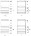
도 1은 본 발명의 제1 실시 예에 따른 표시 장치의 개략적인 단면도이고, 도 2a 및 도 2b는 본 발명의 제1 실시 예에 따른 표시 장치의 개별 서브 화소의 발광 영역에 대한 개략적인 단면도이다.FIG. 1 is a schematic cross-sectional view of a display device according to a first embodiment of the present invention, and FIGS. 2a and 2b are schematic cross-sectional views of light-emitting areas of individual sub-pixels of the display device according to the first embodiment of the present invention.
도 1에서 알 수 있듯이, 본 발명의 제1 실시 예에 따른 표시 장치는 기판(100), 회로 소자층(200), 제1 전극(310, 320, 330, 340), 뱅크(400), 발광층(500), 제2 전극(600), 봉지층(700), 차광층(800), 및 컬러 필터(910, 920, 930)를 포함하여 이루어진다.As can be seen in FIG. 1, a display device according to a first embodiment of the present invention comprises a substrate (100), a circuit element layer (200), a first electrode (310, 320, 330, 340), a bank (400), a light-emitting layer (500), a second electrode (600), an encapsulating layer (700), a light-shielding layer (800), and a color filter (910, 920, 930).
기판(100)은 유리 또는 플라스틱으로 이루어질 수 있지만, 반드시 그에 한정되는 것은 아니고, 실리콘 웨이퍼와 같은 반도체 물질로 이루어질 수도 있다. 기판(100) 상에는 제1 서브 화소(P1), 제2 서브 화소(P2), 제3 서브 화소(P3) 및 제4 서브 화소(P4)가 구비되어 있다. 제1 서브 화소(P1)는 적색(R) 광을 방출하고, 제2 서브 화소(P2)는 녹색(G) 광을 방출하고, 제3 서브 화소(P3)는 청색(B) 광을 방출하고, 제4 서브 화소(P4)는 백색(W) 광을 방출하도록 구비될 수 있지만, 반드시 그에 한정되는 것은 아니다. 각각의 서브 화소(P1, P2, P3, P4)들의 배열 순서는 다양하게 변경될 수 있다.The substrate (100) may be made of glass or plastic, but is not necessarily limited thereto, and may be made of a semiconductor material such as a silicon wafer. A first sub-pixel (P1), a second sub-pixel (P2), a third sub-pixel (P3), and a fourth sub-pixel (P4) are provided on the substrate (100). The first sub-pixel (P1) may be provided to emit red (R) light, the second sub-pixel (P2) to emit green (G) light, the third sub-pixel (P3) to emit blue (B) light, and the fourth sub-pixel (P4) to emit white (W) light, but is not necessarily limited thereto. The arrangement order of each of the sub-pixels (P1, P2, P3, P4) may be changed in various ways.
본 발명의 제1 실시 예에 따른 표시 장치는 발광된 광이 상부 쪽으로 방출되는 소위 상부 발광(Top emission) 방식으로 이루어질 수 있다. 따라서, 기판(100)의 재료로는 투명한 재료뿐만 아니라 불투명한 재료가 이용될 수 있다.The display device according to the first embodiment of the present invention can be formed in a so-called top emission manner in which the emitted light is emitted upward. Accordingly, as the material of the substrate (100), not only a transparent material but also an opaque material can be used.
회로 소자층(200)은 기판(100) 상에 형성되어 있다.The circuit element layer (200) is formed on the substrate (100).
회로 소자층(200)에는 각종 신호 배선들, 박막 트랜지스터, 및 커패시터 등을 포함하는 회로 소자가 서브 화소(P1, P2, P3, P4) 별로 구비되어 있다. 신호 배선들은 게이트 배선, 데이터 배선, 전원 배선, 및 기준 배선을 포함하여 이루어질 수 있고, 박막 트랜지스터는 스위칭 박막 트랜지스터, 구동 박막 트랜지스터 및 센싱 박막 트랜지스터를 포함하여 이루어질 수 있다.The circuit element layer (200) is provided with circuit elements including various signal wires, thin film transistors, and capacitors for each sub-pixel (P1, P2, P3, P4). The signal wires may include gate wires, data wires, power wires, and reference wires, and the thin film transistors may include switching thin film transistors, driving thin film transistors, and sensing thin film transistors.
스위칭 박막 트랜지스터는 게이트 배선에 공급되는 게이트 신호에 따라 스위칭되어 데이터 배선으로부터 공급되는 데이터 전압을 구동 박막 트랜지스터에 공급하는 역할을 한다.The switching thin film transistor is switched according to the gate signal supplied to the gate wiring and supplies the data voltage supplied from the data wiring to the driving thin film transistor.
구동 박막 트랜지스터는 스위칭 박막 트랜지스터로부터 공급되는 데이터 전압에 따라 스위칭되어 전원 배선에서 공급되는 전원으로부터 데이터 전류를 생성하여 제1 전극(310, 320, 330, 340)에 공급하는 역할을 한다.The driving thin film transistor is switched according to the data voltage supplied from the switching thin film transistor and generates a data current from the power supplied from the power wiring and supplies it to the first electrode (310, 320, 330, 340).
센싱 박막 트랜지스터는 화질 저하의 원인이 되는 구동 박막 트랜지스터의 문턱 전압 편차를 센싱하는 역할을 하는 것으로서, 게이트 배선 또는 별도의 센싱 배선에서 공급되는 센싱 제어 신호에 응답하여 구동 박막 트랜지스터의 전류를 기준 배선으로 공급한다.The sensing thin film transistor senses the threshold voltage deviation of the driving thin film transistor, which is the cause of image quality deterioration, and supplies current from the driving thin film transistor to the reference wiring in response to a sensing control signal supplied from the gate wiring or a separate sensing wiring.
커패시터는 구동 박막 트랜지스터에 공급되는 데이터 전압을 한 프레임 동안 유지시키는 역할을 하는 것으로서, 구동 박막 트랜지스터의 게이트 단자 및 소스 단자에 각각 연결된다.The capacitor serves to maintain the data voltage supplied to the driving thin film transistor for one frame, and is connected to the gate terminal and source terminal of the driving thin film transistor, respectively.
제1 전극(310, 320, 330, 340)은 회로 소자층(200) 상에 형성된다. 제1 전극(310, 320, 330, 340)은 각각 서브 화소(P1, P2, P3, P4) 별로 패턴 형성되어 있으며, 표시 장치의 양극(Anode)으로 기능할 수 있다. 제1 전극(310, 320, 330, 340)은 회로 소자층(200)에 구비된 구동 박막 트랜지스터와 연결되어 있다.The first electrodes (310, 320, 330, 340) are formed on the circuit element layer (200). The first electrodes (310, 320, 330, 340) are pattern-formed for each sub-pixel (P1, P2, P3, P4), and can function as an anode of the display device. The first electrodes (310, 320, 330, 340) are connected to the driving thin film transistors provided on the circuit element layer (200).
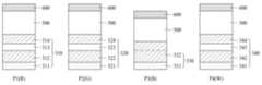
이 때, 제1 전극(310, 320, 330, 340)은 금속 물질로 이루어지므로, 표시 장치의 외부에서 입사되는 광이 반사되어 패널의 시인성이 낮아질 수 있다. 이에 따라, 표시 장치의 외부에서 입사되는 광의 반사율을 저감하기 위하여, 제1 내지 제4 서브 화소(P1-P4) 각각에 구비된 제1 전극(310, 320, 330, 340)들은 서로 상이한 구조로 이루어질 수 있다.At this time, since the first electrodes (310, 320, 330, 340) are made of a metal material, light incident from the outside of the display device may be reflected, thereby reducing the visibility of the panel. Accordingly, in order to reduce the reflectivity of light incident from the outside of the display device, the first electrodes (310, 320, 330, 340) provided in each of the first to fourth sub-pixels (P1-P4) may be formed with different structures.
구체적으로, 도 2a는 제1 서브 화소(P1)에 구비된 제1 전극(310)의 구조를 도시하고 있다. 제1 서브 화소(P1)에 구비된 제1 전극(310)은 광흡수층(311) 및 제1 반투과 전극(312)을 포함한다.Specifically, FIG. 2A illustrates the structure of a first electrode (310) provided in a first sub-pixel (P1). The first electrode (310) provided in the first sub-pixel (P1) includes a light absorption layer (311) and a first semi-transparent electrode (312).
제1 서브 화소(P1)의 광흡수층(311)은 회로 소자층(200) 상에 구비된다. 광흡수층(311)은 광을 흡수하는 물질로 이루어져, 제1 서브 화소(P1)에 입사된 외부의 광을 흡수할 수 있다. 예를 들어, 광흡수층(311)은 크롬(Cr)이나 니켈(Ni) 등의 금속 물질로 이루어질 수 있다. 이 경우, 광흡수층(311)은 전도성을 가지므로, 회로 소자층(200)에 구비된 구동 박막 트랜지스터와 전기적으로 연결될 수 있다. 또는, 광흡수층(311)은 블랙 염료를 포함하는 유기물 또는 무기물로 형성될 수도 있다. 이 경우, 광흡수층(311)은 전도성을 가지지 않으므로, 광흡수층(311)에 컨택홀을 구비하여, 회로 소자층(200)과 제1 반투과 전극(312)을 전기적으로 연결할 수 있다.The light absorption layer (311) of the first sub-pixel (P1) is provided on the circuit element layer (200). The light absorption layer (311) is made of a material that absorbs light and can absorb external light incident on the first sub-pixel (P1). For example, the light absorption layer (311) may be made of a metal material such as chromium (Cr) or nickel (Ni). In this case, since the light absorption layer (311) is conductive, it can be electrically connected to a driving thin film transistor provided in the circuit element layer (200). Alternatively, the light absorption layer (311) may be formed of an organic or inorganic material containing a black dye. In this case, since the light absorption layer (311) is not conductive, a contact hole may be provided in the light absorption layer (311) to electrically connect the circuit element layer (200) and the first semi-transparent electrode (312).
제1 서브 화소(P1)의 제1 반투과 전극(312)은 광흡수층(311)과 발광층(500) 사이에 구비된다. 제1 반투과 전극(312)는 광의 일부를 반사시키고, 광의 나머지 일부는 투과시킬 수 있다. 이에 따라, 제1 반투과 전극(312)에서 반사되는 광은 컬러 필터를 통과하여 제1 서브 화소(P1)를 표시할 수 있으며, 제1 반투과 전극(312)에서 투과되는 광은 제1 반투과 전극(312)의 하부에 구비된 광흡수층(311)에 입사되어 광흡수층(311)에 흡수될 수 있다. 이에 따라, 제1 서브 화소(P1)에서 외부의 광이 반사되는 것을 방지하면서도, 제1 서브 화소(P1)의 발광 효율이 감소되는 것을 최소화할 수 있다. 제1 반투과 전극(312)은 알루미늄(Al), 은(Ag), 구리(Cu), 마그네슘(Mg), 몰리브덴(Mo), 및 티타늄(Ti) 중의 금속 물질 또는 이들의 합금으로 이루어진 단일층 또는 다중층으로 구성될 수 있다.The first semi-transparent electrode (312) of the first sub-pixel (P1) is provided between the light-absorbing layer (311) and the light-emitting layer (500). The first semi-transparent electrode (312) can reflect a portion of light and transmit the remaining portion of light. Accordingly, light reflected from the first semi-transparent electrode (312) can pass through the color filter to display the first sub-pixel (P1), and light transmitted from the first semi-transparent electrode (312) can be incident on the light-absorbing layer (311) provided below the first semi-transparent electrode (312) and absorbed by the light-absorbing layer (311). Accordingly, it is possible to prevent external light from being reflected from the first sub-pixel (P1) while minimizing a decrease in the light-emitting efficiency of the first sub-pixel (P1). The first semi-transparent electrode (312) may be composed of a single layer or multiple layers made of a metal material selected from aluminum (Al), silver (Ag), copper (Cu), magnesium (Mg), molybdenum (Mo), and titanium (Ti), or an alloy thereof.
또한, 도면에 도시되지 않았으나, 제1 서브 화소(P1)에서 광흡수층(311)은 생략될 수도 있다.Additionally, although not shown in the drawing, the light absorption layer (311) may be omitted in the first sub-pixel (P1).
그리고, 도 2b는 제2 서브 화소(P2)에 구비된 제1 전극(320)의 구조를 도시하고 있다. 제2 서브 화소(P2)에 구비된 제1 전극(320)은 광흡수층(321), 제2 반투과 전극(322), 제1 투명 전극(323) 및 제3 반투과 전극(324)을 포함한다.And, Fig. 2b illustrates the structure of the first electrode (320) provided in the second sub-pixel (P2). The first electrode (320) provided in the second sub-pixel (P2) includes a light absorption layer (321), a second semi-transparent electrode (322), a first transparent electrode (323), and a third semi-transparent electrode (324).
제2 서브 화소(P2)의 광흡수층(321)은 회로 소자층(200) 상에 구비된다. 광흡수층(321)은 광을 흡수하는 물질로 이루어져, 제2 서브 화소(P2)에 입사된 외부의 광을 흡수할 수 있다. 예를 들어, 광흡수층(321)은 크롬(Cr)이나 니켈(Ni) 등의 금속 물질로 이루어질 수 있다. 이 경우, 광흡수층(321)은 전도성을 가지므로, 회로 소자층(200)에 구비된 구동 박막 트랜지스터와 전기적으로 연결될 수 있다. 또는, 광흡수층(321)은 블랙 염료를 포함하는 유기물 또는 무기물로 형성될 수도 있다. 이 경우, 광흡수층(321)은 전도성을 가지지 않으므로, 광흡수층(321)에 컨택홀이 구비되어, 회로 소자층(200)과 제2 반투과 전극(322)이 전기적으로 연결될 수 있다. 또한, 제2 서브 화소(P2)에 구비된 광흡수층(321)의 두께는 제1 서브 화소(P1)에 구비된 광흡수층(311)의 두께와 동일하도록 형성될 수 있다.The light absorption layer (321) of the second sub-pixel (P2) is provided on the circuit element layer (200). The light absorption layer (321) is made of a material that absorbs light and can absorb external light incident on the second sub-pixel (P2). For example, the light absorption layer (321) may be made of a metal material such as chromium (Cr) or nickel (Ni). In this case, since the light absorption layer (321) is conductive, it may be electrically connected to a driving thin film transistor provided in the circuit element layer (200). Alternatively, the light absorption layer (321) may be formed of an organic or inorganic material containing a black dye. In this case, since the light absorption layer (321) is not conductive, a contact hole may be provided in the light absorption layer (321) so that the circuit element layer (200) and the second semi-transparent electrode (322) may be electrically connected. Additionally, the thickness of the light absorption layer (321) provided in the second sub-pixel (P2) may be formed to be the same as the thickness of the light absorption layer (311) provided in the first sub-pixel (P1).
제2 서브 화소(P2)의 제2 반투과 전극(322)은 광흡수층(321) 상에 구비된다. 제2 반투과 전극(322)은 광의 일부를 반사시키고, 광의 나머지 일부는 투과시킬 수 있다. 이에 따라, 제2 반투과 전극(322)에서 투과되는 광은 제2 반투과 전극(322)의 하부에 구비된 광흡수층(321)에 입사되어 광흡수층(321)에 흡수될 수 있다. 이 때, 제2 반투과 전극(322)의 두께는 제1 반투과 전극(312)의 두께보다 얇게 형성함으로써, 광의 투과율을 더욱 향상시켜 광흡수층(321)에 흡수되는 광의 양을 증가시킬 수 있다. 또한, 제2 반투과 전극(322)은 알루미늄(Al), 은(Ag), 구리 (Cu), 마그네슘(Mg), 몰리브덴(Mo), 및 티타늄(Ti) 중의 금속 물질 또는 이들의 합금으로 이루어진 단일층 또는 다중층으로 구성될 수 있다.The second semi-transparent electrode (322) of the second sub-pixel (P2) is provided on the light-absorbing layer (321). The second semi-transparent electrode (322) can reflect a portion of the light and transmit the remaining portion of the light. Accordingly, light transmitted through the second semi-transparent electrode (322) can be incident on the light-absorbing layer (321) provided below the second semi-transparent electrode (322) and absorbed by the light-absorbing layer (321). At this time, the thickness of the second semi-transparent electrode (322) is formed thinner than the thickness of the first semi-transparent electrode (312), thereby further improving the light transmittance and increasing the amount of light absorbed by the light-absorbing layer (321). Additionally, the second semi-transparent electrode (322) may be composed of a single layer or multiple layers made of a metal material among aluminum (Al), silver (Ag), copper (Cu), magnesium (Mg), molybdenum (Mo), and titanium (Ti), or an alloy thereof.
제2 서브 화소(P2)의 제1 투명 전극(323)은 제2 반투과 전극(322) 상에 구비되며, 투명한 전도성 물질로 이루어질 수 있다. 예를 들어, 제1 투명 전극(323)은 인듐주석산화물(ITO) 및 인듐아연산화물(IZO)과 같은 투명 전도성 물질의 단일층 또는 다중층으로 이루어질 수 있다.The first transparent electrode (323) of the second sub-pixel (P2) is provided on the second semi-transparent electrode (322) and may be made of a transparent conductive material. For example, the first transparent electrode (323) may be made of a single layer or multiple layers of a transparent conductive material such as indium tin oxide (ITO) and indium zinc oxide (IZO).
제2 서브 화소(P2)의 제3 반투과 전극(324)은 제1 투명 전극(323) 상에 구비된다. 제3 반투과 전극(324)은 광의 일부를 반사시키고, 광의 나머지 일부는 투과시킬 수 있다. 이 때, 제3 반투과 전극(324)의 두께는 제1 반투과 전극(312)의 두께보다 얇게 형성함으로써, 광의 투과율을 더욱 향상시킬 수 있다. 또한, 제3 반투과 전극(324)은 알루미늄(Al), 은(Ag), 구리(Cu), 마그네슘(Mg), 몰리브덴(Mo), 및 티타늄(Ti) 중의 금속 물질 또는 이들의 합금으로 이루어진 단일층 또는 다중층으로 구성될 수 있다.The third semi-transparent electrode (324) of the second sub-pixel (P2) is provided on the first transparent electrode (323). The third semi-transparent electrode (324) can reflect a portion of light and transmit the remaining portion of light. At this time, the thickness of the third semi-transparent electrode (324) can be formed thinner than the thickness of the first semi-transparent electrode (312), thereby further improving the light transmittance. In addition, the third semi-transparent electrode (324) can be formed as a single layer or multiple layers made of a metal material among aluminum (Al), silver (Ag), copper (Cu), magnesium (Mg), molybdenum (Mo), and titanium (Ti), or an alloy thereof.
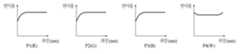
즉, 제2 서브 화소(P2)는 광흡수층(321), 제2 반투과 전극(322), 제1 투명 전극(323) 및 제3 반투과 전극(324)이 순차적으로 적층된 구조의 제1 전극(320)을 포함할 수 있다. 상기 적층 구조를 통해, 제2 서브 화소(P2)는 제1 서브 화소(P1)보다 외부 광의 반사율을 효과적으로 저감할 수 있다. 구체적으로, 외부의 광(L0)이 발광 영역으로 입사되면, 외부의 광(L0)은 제3 반투과 전극(324) 상에서 반사되는 광과 제3 반투과 전극(324)을 통과하는 광으로 분배될 수 있다. 제3 반투과 전극(324) 상에서 반사된 제1 반사광(L1)은 외부로 방출될 수 있다. 그리고, 제3 반투과 전극(324) 및 제1 투명 전극(323)을 통과한 광은 제2 반투과 전극(322)에 의해 제2 반사광(L2) 및 투과광(L3)으로 분배될 수 있다. 제2 반사광(L2)은 제2 반투과 전극(322) 상에서 반사되어 외부로 방출될 수 있으며, 투과광(L3)은 제2 반투과 전극(322)을 통과하여 광흡수층(321)에 흡수될 수 있다.That is, the second sub-pixel (P2) may include a first electrode (320) having a structure in which a light absorbing layer (321), a second semi-transparent electrode (322), a first transparent electrode (323), and a third semi-transparent electrode (324) are sequentially laminated. Through the laminated structure, the second sub-pixel (P2) may effectively reduce the reflectivity of external light more than the first sub-pixel (P1). Specifically, when external light (L0) is incident on the light-emitting region, the external light (L0) may be distributed into light reflected on the third semi-transparent electrode (324) and light passing through the third semi-transparent electrode (324). The first reflected light (L1) reflected on the third semi-transparent electrode (324) may be emitted to the outside. And, light passing through the third semi-transparent electrode (324) and the first transparent electrode (323) can be distributed into second reflected light (L2) and transmitted light (L3) by the second semi-transparent electrode (322). The second reflected light (L2) can be reflected on the second semi-transparent electrode (322) and emitted to the outside, and the transmitted light (L3) can pass through the second semi-transparent electrode (322) and be absorbed by the light absorbing layer (321).
이 때, 외부로 방출된 제1 반사광(L1)과 제2 반사광(L2) 사이에서 부분 상쇄 간섭이 발생할 수 있다. 예를 들어, 제1 반사광(L1)과 제2 반사광(L2)의 광량이 동일하다면, 제1 반사광(L1)과 제2 반사광(L2)은 전부 상쇄될 수 있다. 하지만, 광흡수층(321)에 흡수된 투과광(L3)에 의해 제2 반사광(L2)의 광량은 제1 반사광(L1)의 광량보다 작으므로, 제1 반사광(L1)과 제2 반사광(L2)은 전부 상쇄되지 않고, 일부분만 상쇄될 수 있다. 상쇄되지 않은 반사광은 발광층(500)에서 방출된 광과 함께 화소를 표시할 때 이용할 수 있으므로, 외부 광의 반사율을 저감하면서도, 휘도의 감소를 최소화할 수 있다.At this time, partial destructive interference may occur between the first reflected light (L1) and the second reflected light (L2) emitted to the outside. For example, if the light quantities of the first reflected light (L1) and the second reflected light (L2) are the same, the first reflected light (L1) and the second reflected light (L2) may be completely canceled out. However, since the light quantity of the second reflected light (L2) is smaller than that of the first reflected light (L1) due to the transmitted light (L3) absorbed by the light-absorbing layer (321), the first reflected light (L1) and the second reflected light (L2) may not be completely canceled out, but may be only partially canceled out. Since the reflected light that is not canceled out can be used when displaying a pixel together with the light emitted from the light-emitting layer (500), the reflectivity of the external light can be reduced while minimizing the decrease in brightness.
따라서, 본 발명의 제1 실시 예에 따르면, 제1 서브 화소(P1)의 제1 반투과 전극(312)보다 얇은 두께로 형성되어, 제1 서브 화소(P1)의 제1 반투과 전극(312)보다 투과율이 향상된 제2 및 제3 반투과 전극(322, 324) 사이에 제1 투명 전극(323)을 형성함으로써, 제2 서브 화소(P1)의 제1 전극(320)은 모든 파장에 대하여 외부 광의 반사율을 제1 서브 화소(P1)의 제1 전극(310)보다 더 저감할 수 있다. 특히, 패널의 시인성에 가장 큰 영향을 미치는 광인 녹색(G) 광의 파장대의 반사율을 저감할 수 있다. 예를 들어, 550nm 파장대의 광의 반사율을 효과적으로 저감할 수 있다.Therefore, according to the first embodiment of the present invention, by forming the first transparent electrode (323) between the second and third transflective electrodes (322, 324) which are formed with a thickness thinner than the first transflective electrode (312) of the first sub-pixel (P1) and have improved transmittance than the first transflective electrode (312) of the first sub-pixel (P1), the first electrode (320) of the second sub-pixel (P1) can reduce the reflectance of external light for all wavelengths more than the first electrode (310) of the first sub-pixel (P1). In particular, the reflectance of the wavelength of green (G) light, which has the greatest influence on the visibility of the panel, can be reduced. For example, the reflectance of light with a wavelength of 550 nm can be effectively reduced.
제2 반투과 전극(322) 및 제3 반투과 전극(324)은 상이한 물질로 이루어질 수 있다. 그리고, 제2 반투과 전극(322) 및 제3 반투과 전극(324)은 반사율이 유사한 물질을 사용함으로써, 광의 각 파장대에 대한 반사율의 스펙트럼을 정교하게 설정할 수 있다.The second semi-transparent electrode (322) and the third semi-transparent electrode (324) can be made of different materials. In addition, the second semi-transparent electrode (322) and the third semi-transparent electrode (324) can precisely set the spectrum of reflectivity for each wavelength of light by using materials having similar reflectivity.
또한, 제1 내지 제3 반투과 전극(312, 322, 324)은 동일한 물질로 이루어질 수 있다. 특히, 패널의 시인성에 가장 큰 영향을 미치는 광인 녹색(G) 광의 파장대의 광 반사율을 저감하기 위하여, 제2 반투과 전극(322)의 두께는 제3 투과 전극(324)의 두께보다 두껍게 형성될 수 있다. 예를 들어, 550nm 파장대의 광의 반사율을 더욱 저감시키기 위해서, 제2 반투과 전극(322)의 두께는 제3 반투과 전극(324)의 두께보다 두껍게 형성될 수 있다.In addition, the first to third semi-transparent electrodes (312, 322, 324) may be formed of the same material. In particular, in order to reduce light reflectance in the wavelength range of green (G) light, which has the greatest influence on the visibility of the panel, the thickness of the second semi-transparent electrode (322) may be formed thicker than the thickness of the third transmissive electrode (324). For example, in order to further reduce light reflectance in the wavelength range of 550 nm, the thickness of the second semi-transparent electrode (322) may be formed thicker than the thickness of the third semi-transmissive electrode (324).
또한, 공정 과정의 간소화를 위해, 제1 반투과 전극(312)의 두께가 제2 반투과 전극(322)의 두께와 제3 반투과 전극(324)의 두께의 합과 동일하도록 형성할 수 있다. 구체적으로, 제2 반투과 전극(322)을 형성하는 공정에서, 제1 반투과 전극(312)의 하부 영역을 동시에 형성할 수 있다. 그 후에, 제2 반투과 전극(322) 상에 제1 투명 전극(323)을 형성할 수 있다. 그리고, 제1 투명 전극(323) 상에 제3 반투과 전극(324)을 형성하는 공정에서, 제1 반투과 전극(312)의 상부 영역을 동시에 형성할 수 있다. 즉, 제2 반투과 전극(322) 및 제3 반투과 전극(324)를 형성하는 공정 과정에서 제1 반투과 전극(312)을 동시에 형성함으로써, 제1 반투과 전극(312)을 형성하는 추가적인 공정을 생략할 수 있다. 이에 따라, 제1 반투과 전극(312)은 이중층으로 형성될 수 있으며, 제2 반투과 전극(322)의 두께와 제3 반투과 전극(324) 두께의 합과 동일한 두께로 형성될 수 있다. 또한, 제1 내지 제3 반투과 전극(312, 322, 324)이 동일한 물질로 이루어질 경우, 제1 반투과 전극(312)은 단일층으로 보일 수 있다.In addition, in order to simplify the manufacturing process, the thickness of the first semi-transparent electrode (312) may be formed to be equal to the sum of the thicknesses of the second semi-transparent electrode (322) and the third semi-transparent electrode (324). Specifically, in the process of forming the second semi-transparent electrode (322), the lower region of the first semi-transparent electrode (312) may be formed simultaneously. Thereafter, the first transparent electrode (323) may be formed on the second semi-transparent electrode (322). Then, in the process of forming the third semi-transparent electrode (324) on the first transparent electrode (323), the upper region of the first semi-transparent electrode (312) may be formed simultaneously. That is, by forming the first semi-transparent electrode (312) simultaneously in the process of forming the second semi-transparent electrode (322) and the third semi-transparent electrode (324), the additional process of forming the first semi-transparent electrode (312) may be omitted. Accordingly, the first semi-transparent electrode (312) may be formed as a double layer, and may be formed with a thickness equal to the sum of the thickness of the second semi-transparent electrode (322) and the thickness of the third semi-transparent electrode (324). In addition, when the first to third semi-transparent electrodes (312, 322, 324) are made of the same material, the first semi-transparent electrode (312) may appear as a single layer.
도 3a에 도시된 바와 같이, 제2 서브 화소(P2)에 구비된 제1 전극(320)은 제2 투명 전극(325)을 더 포함할 수 있다. 도 3a를 참조하면, 제2 투명 전극(325)은 제3 반투과 전극(324)과 발광층(500) 사이에 구비되어, 제3 반투과 전극(324)의 일 함수와 발광층(500)의 일 함수의 차이를 감소시킬 수 있다.As illustrated in FIG. 3A, the first electrode (320) provided in the second sub-pixel (P2) may further include a second transparent electrode (325). Referring to FIG. 3A, the second transparent electrode (325) is provided between the third semi-transparent electrode (324) and the light-emitting layer (500), thereby reducing the difference between the work function of the third semi-transparent electrode (324) and the work function of the light-emitting layer (500).
또한, 도 3b를 참조하면, 제2 투명 전극(325)은 광흡수층(321)과 제2 반투과 전극(322) 사이에 구비되어, 광흡수층(321)과 제2 반투과 전극(322)의 접착력을 향상시킬 수 있다. 그리고, 제2 투명 전극(325)는 제1 투명 전극(323)과 동일한 물질로 형성될 수 있다.In addition, referring to FIG. 3b, the second transparent electrode (325) is provided between the light absorbing layer (321) and the second semi-transparent electrode (322), thereby improving the adhesive strength between the light absorbing layer (321) and the second semi-transparent electrode (322). In addition, the second transparent electrode (325) can be formed of the same material as the first transparent electrode (323).
또는, 도 3c를 참조하면, 제2 투명 전극(325)은 제3 반투과 전극(324)과 발광층(500) 사이 및 광흡수층(321)과 제2 반투과 전극(322) 사이에 모두 구비될 수 있다. 이에 따라, 제3 반투과 전극(324)의 일 함수와 발광층(500)의 일 함수의 차이를 감소시키면서, 광흡수층(321)과 제2 반투과 전극(322)의 접착력을 향상시킬 수 있다. 그리고, 복수의 제2 투명 전극(325)은 제1 투명 전극(323)과 동일한 물질로 형성될 수 있다.Alternatively, referring to FIG. 3c, the second transparent electrode (325) may be provided both between the third semi-transparent electrode (324) and the light-emitting layer (500) and between the light-absorbing layer (321) and the second semi-transparent electrode (322). Accordingly, the difference between the work function of the third semi-transparent electrode (324) and the work function of the light-absorbing layer (500) may be reduced, while improving the adhesion between the light-absorbing layer (321) and the second semi-transparent electrode (322). In addition, the plurality of second transparent electrodes (325) may be formed of the same material as the first transparent electrode (323).
또는, 도 3d를 참조하면, 광흡수층(321) 하부에 반사 전극(326)을 구비할 수 있다. 반사 전극(326)은 광흡수층(321)에서 흡수되지 않은 외부 광을 반사시켜, 광흡수층(321)에 흡수될 수 있도록 광의 경로를 변경할 수 있다. 그리고, 반사 전극(326)은 제2 및 제3 반투과 전극(322, 324)과 동일한 물질로 형성될 수 있으며, 제2 및 제3 반투과 전극(322, 324)보다 두껍게 형성될 수 있다. 반사 전극(326)을 제2 및 제3 반투과 전극(322, 324)보다 두껍게 형성함으로써, 제2 반투과 전극(322)과 제3 반투과 전극(324)의 두께 편차를 감소시킬 수 있다.Alternatively, referring to FIG. 3d, a reflective electrode (326) may be provided under the light-absorbing layer (321). The reflective electrode (326) may reflect external light that is not absorbed by the light-absorbing layer (321) and change the path of the light so that it can be absorbed by the light-absorbing layer (321). In addition, the reflective electrode (326) may be formed of the same material as the second and third semi-transparent electrodes (322, 324) and may be formed thicker than the second and third semi-transparent electrodes (322, 324). By forming the reflective electrode (326) thicker than the second and third semi-transparent electrodes (322, 324), the thickness difference between the second semi-transparent electrode (322) and the third semi-transparent electrode (324) may be reduced.
도 4a 내지 도 4f는 본 발명의 제1 실시 예에 따른 표시 장치의 제1 내지 제4 서브 화소(P1-P4)의 발광 영역에 대한 개략적인 단면도이다.FIGS. 4A to 4F are schematic cross-sectional views of light-emitting areas of first to fourth sub-pixels (P1 to P4) of a display device according to a first embodiment of the present invention.
도 4a를 참조하면, 제3 서브 화소(P3)의 제1 전극(330)은 제1 서브 화소(P1)의 제1 전극(310)과 동일한 구조로 형성될 수 있다. 즉, 제3 서브 화소(P3)의 제1 전극(330)은 광흡수층(331) 및 제1 반투과 전극(332)을 포함하여 이루어질 수 있다. 이에 따라, 제3 서브 화소(P3)의 발광 효율이 감소되는 것을 최소화하면서, 제3 서브 화소(P3)에서 외부의 광이 반사되는 것을 방지할 수 있다. 또한, 제1 서브 화소(P1)의 제1 전극(310)이 광흡수층(311)을 포함하지 않는 경우, 제3 서브 화소(P3)의 제1 전극(330)도 광흡수층(331)을 포함하지 않을 수 있다.Referring to FIG. 4A, the first electrode (330) of the third sub-pixel (P3) may be formed with the same structure as the first electrode (310) of the first sub-pixel (P1). That is, the first electrode (330) of the third sub-pixel (P3) may include a light absorption layer (331) and a first transflective electrode (332). Accordingly, it is possible to prevent external light from being reflected from the third sub-pixel (P3) while minimizing a decrease in the light emission efficiency of the third sub-pixel (P3). In addition, when the first electrode (310) of the first sub-pixel (P1) does not include the light absorption layer (311), the first electrode (330) of the third sub-pixel (P3) may also not include the light absorption layer (331).
또한, 제4 서브 화소(P4)의 제1 전극은(340)은 제2 서브 화소(P2)의 제1 전극(320)과 동일한 구조로 형성될 수 있다. 즉, 제4 서브 화소(P4)의 제1 전극(340)은 광흡수층(341), 제2 반투과 전극(342), 제1 투명 전극(343) 및 제3 반투과 전극(344)을 포함하여 이루어질 수 있다. 이에 따라, 패널의 시인성에 가장 큰 영향을 미치는 광인 녹색(G) 광의 파장대, 즉, 550nm 파장대의 광의 반사율을 더욱 저감시킬 수 있다.In addition, the first electrode (340) of the fourth sub-pixel (P4) may be formed with the same structure as the first electrode (320) of the second sub-pixel (P2). That is, the first electrode (340) of the fourth sub-pixel (P4) may include a light absorption layer (341), a second semi-transparent electrode (342), a first transparent electrode (343), and a third semi-transparent electrode (344). Accordingly, the reflectance of the wavelength of green (G) light, which has the greatest influence on the visibility of the panel, i.e., light with a wavelength of 550 nm, can be further reduced.
도 4b를 참조하면, 제1 서브 화소(P1)의 제1 전극(310)이 제2 서브 화소(P2) 및 제4 서브 화소(P4)의 제1 전극(320, 340)과 동일한 구조로 형성될 수 있다. 즉, 제1 서브 화소(P1)의 제1 전극(310)은 광흡수층(311), 제2 반투과 전극(312), 제1 투명 전극(313) 및 제3 반투과 전극(314)을 포함하여 이루어질 수 있다.Referring to FIG. 4b, the first electrode (310) of the first sub-pixel (P1) may be formed with the same structure as the first electrodes (320, 340) of the second sub-pixel (P2) and the fourth sub-pixel (P4). That is, the first electrode (310) of the first sub-pixel (P1) may include a light absorption layer (311), a second semi-transparent electrode (312), a first transparent electrode (313), and a third semi-transparent electrode (314).
도 4c를 참조하면, 제3 서브 화소(P3)의 제1 전극(330)이 제2 서브 화소(P2) 및 제4 서브 화소(P4)의 제1 전극(320, 340)과 동일한 구조로 형성될 수 있다. 즉, 제3 서브 화소(P3)의 제1 전극(330)은 광흡수층(331), 제2 반투과 전극(332), 제1 투명 전극(333) 및 제3 반투과 전극(334)을 포함하여 이루어질 수 있다.Referring to FIG. 4c, the first electrode (330) of the third sub-pixel (P3) may be formed with the same structure as the first electrodes (320, 340) of the second sub-pixel (P2) and the fourth sub-pixel (P4). That is, the first electrode (330) of the third sub-pixel (P3) may include a light absorption layer (331), a second semi-transparent electrode (332), a first transparent electrode (333), and a third semi-transparent electrode (334).
도 4d를 참조하면, 제1 내지 제4 서브 화소(P1-P4)의 제1 전극(310, 320, 330, 340)이 모두 동일한 적층 구조로 형성될 수 있다. 이 경우, 제1 내지 제4 서브 화소(P1-P4)의 제1 전극(310, 320, 330, 340)을 형성하는 공정에서, 추가적인 패터닝 공정을 생략할 수 있으므로, 공정 과정을 간소화할 수 있다.Referring to FIG. 4d, the first electrodes (310, 320, 330, 340) of the first to fourth sub-pixels (P1-P4) can all be formed with the same laminated structure. In this case, in the process of forming the first electrodes (310, 320, 330, 340) of the first to fourth sub-pixels (P1-P4), an additional patterning process can be omitted, so the process can be simplified.
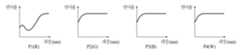
도 4e를 참조하면, 제1 내지 제3 서브 화소(P1-P3)의 제1 전극(310, 320, 330)은 동일한 구조로 형성되고, 제4 서브 화소(P4)의 제1 전극(340)만 상이한 구조로 형성될 수 있다. 즉, 제1 내지 제3 서브 화소(P1-P3)의 제1 전극(310, 320, 330)은 광흡수층(311, 321, 331) 및 제1 반투과 전극(312, 322, 332)을 포함하여 이루어지고, 제4 서브 화소(P4)의 제1 전극(340)은 광흡수층(341), 제2 반투과 전극(342), 제1 투명 전극(343) 및 제3 반투과 전극(344)을 포함하여 이루어질 수 있다. 이 때, 도 4e의 제4 서브 화소(P4)의 제1 전극(340)에서, 광흡수층(341), 제2 반투과 전극(342), 제1 투명 전극(343) 및 제3 반투과 전극(344) 각각을 이루는 물질 또는 각각의 두께를 조절함으로써, 광의 각 파장대에 대한 반사율의 스펙트럼을 정교하게 설정할 수 있다. 또한, 제1 내지 제4 서브 화소(P1-P4)의 제1 전극(310, 320, 330, 340) 각각의 광흡수층(311, 321, 331, 341)은 형성되지 않을 수도 있다.Referring to FIG. 4e, the first electrodes (310, 320, 330) of the first to third sub-pixels (P1-P3) may be formed with the same structure, and only the first electrode (340) of the fourth sub-pixel (P4) may be formed with a different structure. That is, the first electrodes (310, 320, 330) of the first to third sub-pixels (P1-P3) may include a light absorption layer (311, 321, 331) and a first semi-transparent electrode (312, 322, 332), and the first electrode (340) of the fourth sub-pixel (P4) may include a light absorption layer (341), a second semi-transparent electrode (342), a first transparent electrode (343), and a third semi-transparent electrode (344). At this time, in the first electrode (340) of the fourth sub-pixel (P4) of Fig. 4e, by controlling the material or thickness of each of the light-absorbing layer (341), the second semi-transparent electrode (342), the first transparent electrode (343), and the third semi-transparent electrode (344), the spectrum of reflectivity for each wavelength band of light can be precisely set. In addition, the light-absorbing layer (311, 321, 331, 341) of each of the first electrodes (310, 320, 330, 340) of the first to fourth sub-pixels (P1-P4) may not be formed.
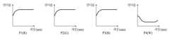
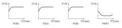
예를 들어, 도 4f를 참조하면, 제1 내지 제3 서브 화소(P1-P3)의 제1 전극(310, 320, 330)의 모든 파장대에 대한 반사율에 비해, 제4 서브 화소(P4)의 제1 전극(340)의 모든 파장대에 대한 반사율이 낮도록 설정할 수 있다. 이에 따라, 시감 반사율 특성에 가장 민감한 백색(W) 화소의 반사율을 저감함으로써, 패널 반사율을 저감할 수 있다.For example, referring to FIG. 4F, the reflectivity of the first electrode (340) of the fourth sub-pixel (P4) for all wavelengths can be set lower than the reflectivity of the first electrode (310, 320, 330) of the first to third sub-pixels (P1-P3) for all wavelengths. Accordingly, the panel reflectivity can be reduced by reducing the reflectivity of the white (W) pixel, which is most sensitive to the luminous reflectivity characteristic.
또는, 도 4g를 참조하면, 제1 내지 제3 서브 화소(P1-P3)의 제1 전극(310, 320, 330)의 청색(B) 광의 파장대에 대한 반사율에 비해, 제4 서브 화소(P4)의 제1 전극(340)의 청색(B) 광의 파장대, 즉, 400nm~500nm 파장대의 광의 반사율이 높도록 설정할 수 있다. 이에 따라, 청색(B) 광의 휘도를 향상시켜, 백색(W) 광의 색온도를 높일 수 있다.Alternatively, referring to FIG. 4g, the reflectance of the blue (B) light wavelength, that is, light in the wavelength range of 400 nm to 500 nm, of the first electrode (340) of the fourth sub-pixel (P4) may be set to be higher than the reflectance of the blue (B) light wavelength of the first electrode (310, 320, 330) of the first to third sub-pixels (P1-P3). Accordingly, the luminance of the blue (B) light can be improved, thereby increasing the color temperature of the white (W) light.
도 4h를 참조하면, 제1 및 제4 서브 화소(P1, P4)의 제1 전극(310, 340)은 동일한 구조로 형성될 수 있다. 즉, 제1 및 제4 서브 화소(P1, P4)의 제1 전극(310, 340)은 광흡수층(311, 341), 제2 반투과 전극(312, 342), 제1 투명 전극(313, 343) 및 제3 반투과 전극(314, 344)을 포함하여 이루어질 수 있다. 이 때, 제1 서브 화소(P1)의 제1 전극(310)을 이루는 광흡수층(311), 제2 반투과 전극(312), 제1 투명 전극(313) 및 제3 반투과 전극(314) 각각을 이루는 물질 또는 각각의 두께를 조절함으로써, 광의 각 파장대에 대한 반사율의 스펙트럼을 정교하게 설정할 수 있다. 또한, 제1 내지 제4 서브 화소(P1-P4)의 제1 전극(310, 320, 330, 340) 각각의 광흡수층(311, 321, 331, 341)은 형성되지 않을 수도 있다.Referring to FIG. 4h, the first electrodes (310, 340) of the first and fourth sub-pixels (P1, P4) may be formed with the same structure. That is, the first electrodes (310, 340) of the first and fourth sub-pixels (P1, P4) may include a light-absorbing layer (311, 341), a second semi-transparent electrode (312, 342), a first transparent electrode (313, 343), and a third semi-transparent electrode (314, 344). At this time, by controlling the material or the thickness of each of the light-absorbing layer (311), the second semi-transparent electrode (312), the first transparent electrode (313), and the third semi-transparent electrode (314) forming the first electrode (310) of the first sub-pixel (P1), the spectrum of reflectivity for each wavelength band of light can be precisely set. Additionally, the light absorption layer (311, 321, 331, 341) of each of the first electrodes (310, 320, 330, 340) of the first to fourth sub-pixels (P1-P4) may not be formed.
예를 들어, 도 4i를 참조하면, 제2 내지 제4 서브 화소(P2-P4)의 제1 전극(320, 330, 340)의 적색(R) 광의 파장대에 대한 반사율에 비해, 제1 서브 화소(P1)의 제1 전극(310)의 적색(R) 광의 파장대에 대한 반사율이 높도록 설정할 수 있다. 또한, 제2 내지 제4 서브 화소(P2-P4)의 제1 전극(320, 330, 340)의 녹색(G) 및 청색(B) 광의 반사율에 비해, 제1 서브 화소(P1)의 제1 전극(310)의 적색(R) 광의 파장대에 대한 반사율이 낮도록 설정할 수 있다. 이에 따라, 적색(R) 광의 순색을 향상시킬 수 있다.For example, referring to FIG. 4i, the reflectivity of the first electrode (310) of the first sub-pixel (P1) for the red (R) light wavelength range may be set to be higher than the reflectivity of the first electrodes (320, 330, 340) of the second to fourth sub-pixels (P2-P4) for the red (R) light wavelength range. In addition, the reflectivity of the first electrode (310) of the first sub-pixel (P1) for the red (R) light wavelength range may be set to be lower than the reflectivity of the first electrodes (320, 330, 340) of the second to fourth sub-pixels (P2-P4) for the green (G) and blue (B) light wavelength range. Accordingly, the pure color of the red (R) light can be improved.
도 1을 참조하면, 뱅크(400)는 복수의 서브 화소(P1, P2, P3, P4) 사이의 경계에서, 제1 전극(310, 320, 330, 340) 상에서 매트릭스 구조로 형성되면서 복수의 서브 화소(P1, P2, P3, P4) 각각에 발광 영역을 정의한다. 즉, 각각의 서브 화소(P1, P2, P3, P4)에서 뱅크(400)가 형성되지 않은 개구 영역이 발광 영역이 된다.Referring to FIG. 1, a bank (400) is formed in a matrix structure on the first electrode (310, 320, 330, 340) at the boundary between a plurality of sub-pixels (P1, P2, P3, P4) and defines a light-emitting area for each of the plurality of sub-pixels (P1, P2, P3, P4). That is, an aperture area in each sub-pixel (P1, P2, P3, P4) where a bank (400) is not formed becomes a light-emitting area.
뱅크(400)는 아크릴 수지(acryl resin), 에폭시 수지(epoxy resin), 페놀 수지(phenolic resin), 폴리아미드 수지(polyamide resin), 폴리이미드 수지(polyimide resin) 등의 유기막으로 형성될 수 있다. 또는 뱅크(320)는 실리콘 질화물, 알루미늄 질화물, 지르코늄 질화물, 티타늄 질화물, 하프늄 질화물, 탄탈륨 질화물, 실리콘 산화물, 알루미늄 산화물, 또는 티타늄 산화물 등의 무기막으로 형성될 수도 있다.The bank (400) may be formed of an organic film such as an acrylic resin, an epoxy resin, a phenolic resin, a polyamide resin, or a polyimide resin. Alternatively, the bank (320) may be formed of an inorganic film such as silicon nitride, aluminum nitride, zirconium nitride, titanium nitride, hafnium nitride, tantalum nitride, silicon oxide, aluminum oxide, or titanium oxide.
발광층(500)은 제1 전극(310, 320, 330, 340) 상에 형성된다. 발광층(500)은 뱅크(400) 상에도 형성될 수 있다. 즉, 발광층(500)은 각각의 서브 화소(P1, P2, P3, P4) 및 그들 사이의 경계 영역에도 형성된다.The light-emitting layer (500) is formed on the first electrode (310, 320, 330, 340). The light-emitting layer (500) may also be formed on the bank (400). That is, the light-emitting layer (500) is also formed on each of the sub-pixels (P1, P2, P3, P4) and the boundary area between them.
발광층(500)은 정공 수송층(hole transporting layer), 발광층(light emitting layer), 및 전자 수송층(electron transporting layer)을 포함할 수 있다. 이 경우, 제1 전극(310, 320, 330, 340)과 제2 전극(600)에 전압이 인가되면 정공과 전자가 각각 정공 수송층과 전자 수송층을 통해 발광층으로 이동하게 되며, 발광층에서 서로 결합하여 발광하게 된다.The light emitting layer (500) may include a hole transporting layer, a light emitting layer, and an electron transporting layer. In this case, when voltage is applied to the first electrode (310, 320, 330, 340) and the second electrode (600), holes and electrons move to the light emitting layer through the hole transporting layer and the electron transporting layer, respectively, and combine with each other in the light emitting layer to emit light.
발광층(500)은 백색(W) 광을 발광하도록 구비될 수 있다. 이를 위해서, 발광층(500)은 서로 상이한 색상의 광을 발광하는 복수의 스택(stack)을 포함하여 이루어질 수 있다. 또한, 발광층(500)이 백색(W)을 발광하도록 이루어진 경우, 발광층(500)은 서브 화소(P1, P2, P3, P4) 별로 동일한 물질로 동일한 두께로 형성될 수 있다.The light-emitting layer (500) may be configured to emit white (W) light. To this end, the light-emitting layer (500) may be configured to include a plurality of stacks that emit light of different colors. In addition, when the light-emitting layer (500) is configured to emit white (W), the light-emitting layer (500) may be formed of the same material and with the same thickness for each sub-pixel (P1, P2, P3, P4).
제2 전극(600)은 발광층(500) 상에 형성되어 있다. 제2 전극(600)은 표시 장치의 음극(Cathode)으로 기능할 수 있다. 제2 전극(600)은 발광층(500)과 마찬가지로 각각의 서브 화소(P1, P2, P3, P4) 및 그들 사이의 경계 영역에도 형성된다. 즉, 제2 전극(600)은 제1 전극(310, 320, 330, 340)의 위쪽 및 뱅크(400)의 위쪽에도 형성될 수 있다.The second electrode (600) is formed on the light-emitting layer (500). The second electrode (600) can function as a cathode of the display device. The second electrode (600) is formed in each sub-pixel (P1, P2, P3, P4) and the boundary area between them, similar to the light-emitting layer (500). That is, the second electrode (600) can also be formed above the first electrodes (310, 320, 330, 340) and above the bank (400).
본 발명의 제1 실시 예에 따른 표시 장치는 상부 발광 방식으로 이루어지기 때문에, 제2 전극(600)은 발광층(500)에서 발광된 광을 상부 쪽으로 투과시키기 위해서, 인듐주석산화물(ITO) 또는 인듐아연산화물(IZO)과 같은 투명한 금속물질로 이루어질 수 있다. 그리고, 제2 전극(600)은 단일층 또는 다중층으로 이루어질 수 있다.Since the display device according to the first embodiment of the present invention is formed in a top-emitting manner, the second electrode (600) may be formed of a transparent metal material, such as indium tin oxide (ITO) or indium zinc oxide (IZO), in order to transmit light emitted from the light-emitting layer (500) upward. In addition, the second electrode (600) may be formed in a single layer or multiple layers.
봉지층(700)은 제2 전극(600) 상에 형성되어 발광층(500)으로 외부의 수분이 침투하는 것을 방지하는 역할을 한다. 이와 같은 봉지층(700)은 무기절연물로 이루어질 수도 있다. 또는, 봉지층(700)은 복수의 무기절연물과 적어도 하나의 유기절연물이 적층된 구조로 이루어질 수도 있지만, 반드시 그에 한정되는 것은 아니다. 예를 들어, 봉지층(700)은 유기 절연물을 사이에 두고 제1 무기절연물과 제2 무기절연물이 중첩하도록 형성될 수 있다.The sealing layer (700) is formed on the second electrode (600) and serves to prevent external moisture from penetrating into the light-emitting layer (500). Such a sealing layer (700) may be formed of an inorganic insulating material. Alternatively, the sealing layer (700) may be formed of a structure in which a plurality of inorganic insulating materials and at least one organic insulating material are laminated, but is not necessarily limited thereto. For example, the sealing layer (700) may be formed such that a first inorganic insulating material and a second inorganic insulating material overlap each other with an organic insulating material therebetween.
차광층(800)은 봉지층(700) 상에 형성되어 있다. 차광층(800)은 복수의 서브 화소(P1, P2, P3, P4) 사이의 경계에 매트릭스 구조로 형성되어 서브 화소(P1, P2, P3, P4) 사이의 경계에서 빛샘이 발생하는 것을 방지한다.The light-shielding layer (800) is formed on the sealing layer (700). The light-shielding layer (800) is formed in a matrix structure at the boundary between a plurality of sub-pixels (P1, P2, P3, P4) to prevent light leakage from occurring at the boundary between the sub-pixels (P1, P2, P3, P4).
컬러 필터(910, 920, 930)는 차광층(800)과 봉지층(700) 상에 형성되어 있다. 도면에는 컬러 필터(910, 920, 930)가 차광층(800)의 상면에 형성된 모습을 도시하였지만, 반드시 그에 한정되는 것은 아니고, 차광층(800)이 컬러 필터(910, 920, 930)의 상면에 형성될 수도 있다.The color filters (910, 920, 930) are formed on the light-shielding layer (800) and the sealing layer (700). Although the drawing shows the color filters (910, 920, 930) formed on the upper surface of the light-shielding layer (800), it is not necessarily limited thereto, and the light-shielding layer (800) may be formed on the upper surface of the color filters (910, 920, 930).
컬러 필터(910, 920, 930)는 제1 서브 화소(P1)에 구비된 적색(R)의 제1 컬러 필터(910), 제2 서브 화소(P2)에 구비된 녹색(G)의 제2 컬러 필터(920), 및 제3 서브 화소(P3)에 구비된 청색(B)의 제3 컬러 필터(930)를 포함하여 이루어진다. 따라서, 제1 서브 화소(P1)에서는 발광층(500)에서 발광된 백색(W) 광이 적색(R)의 제1 컬러 필터(910)를 통과하면서 적색(R)의 광만이 투과하게 되고, 제2 서브 화소(P3)에서는 발광층(500)에서 발광된 백색(W) 광이 녹색(G)의 제2 컬러 필터(920)를 통과하면서 녹색(G)의 광만이 투과하게 된다. 그리고, 제3 서브 화소(P3)에서는 발광층(500)에서 발광된 백색(W) 광이 청색(B)의 제3 컬러 필터(930)를 통과하면서 청색(B)의 광만이 투과하게 된다. 제4 서브 화소(P4)에는 컬러 필터가 구비되지 않으므로, 제4 서브 화소(P4)에서는 발광층(500)에서 발광된 백색(W) 광이 그대로 방출된다.The color filters (910, 920, 930) include a first color filter (910) of red (R) provided in the first sub-pixel (P1), a second color filter (920) of green (G) provided in the second sub-pixel (P2), and a third color filter (930) of blue (B) provided in the third sub-pixel (P3). Therefore, in the first sub-pixel (P1), white (W) light emitted from the light-emitting layer (500) passes through the first color filter (910) of red (R) so that only red (R) light is transmitted, and in the second sub-pixel (P3), white (W) light emitted from the light-emitting layer (500) passes through the second color filter (920) of green (G) so that only green (G) light is transmitted. And, in the third sub-pixel (P3), white (W) light emitted from the light-emitting layer (500) passes through the third color filter (930) of blue (B), so that only blue (B) light is transmitted. Since the fourth sub-pixel (P4) does not have a color filter, white (W) light emitted from the light-emitting layer (500) is emitted as is in the fourth sub-pixel (P4).
도시하지는 않았지만, 컬러 필터(910, 920, 930) 상에 보호 필름이 추가로 구비될 수 있다.Although not shown, a protective film may additionally be provided on the color filters (910, 920, 930).
따라서, 본 발명의 제1 실시 예에서는 상부 발광 방식의 표시 장치에서 각 서브 화소(P1, P2, P3, P4)에 구비된 제1 전극(310, 320, 330, 340)의 각각의 구조를 상이하게 형성함으로써, 외부 광의 반사율을 저감하여 패널의 시인성을 향상시키는 효과가 있다.Therefore, in the first embodiment of the present invention, by forming the structure of each of the first electrodes (310, 320, 330, 340) provided in each sub-pixel (P1, P2, P3, P4) differently in a top-emitting display device, there is an effect of reducing the reflectivity of external light and improving the visibility of the panel.
제2 실시 예Second embodiment
도 5는 본 발명의 제2 실시 예에 따른 표시 장치의 개략적인 단면도이며, 도 6a 및 도 6b는 본 발명의 제2 실시 예에 따른 표시 장치의 개별 서브 화소의 발광 영역에 대한 개략적인 단면도로서, 이는 전술한 도 1, 도 2a 및 도 2b에 따른 표시 장치에서 컬러 필터(910, 920, 930)의 형성 위치와 제1 전극(310, 320, 330, 340) 및 제2 전극(600)의 구조가 변경된 것이다. 이하에서는 상이한 구성에 대해서만 설명하기로 한다.FIG. 5 is a schematic cross-sectional view of a display device according to a second embodiment of the present invention, and FIGS. 6A and 6B are schematic cross-sectional views of light-emitting areas of individual sub-pixels of the display device according to the second embodiment of the present invention, which are different from the display devices according to FIGS. 1, 2A and 2B in that the formation positions of the color filters (910, 920, 930) and the structures of the first electrodes (310, 320, 330, 340) and the second electrodes (600) are changed. Hereinafter, only the different configurations will be described.
본 발명의 제2 실시 예에 따른 표시 장치는 발광된 광이 하부 쪽으로 방출되는 소위 하부 발광(Bottom emission) 방식으로 이루어지므로, 기판(100)은 투명한 재료로 이루어질 수 있다.Since the display device according to the second embodiment of the present invention is formed in a so-called bottom emission manner in which the emitted light is emitted downward, the substrate (100) can be formed of a transparent material.
또한, 컬러 필터(910, 920, 930)는 회로 소자층(200) 상에 형성되어 있다. 도면에는 컬러 필터(910, 920, 930)가 차광층(800)의 상면에 형성된 모습을 도시하였지만, 반드시 그에 한정되는 것은 아니고, 차광층(800)이 컬러 필터(910, 920, 930)의 상면에 형성될 수도 있다.In addition, the color filters (910, 920, 930) are formed on the circuit element layer (200). Although the drawing shows the color filters (910, 920, 930) formed on the upper surface of the light-shielding layer (800), it is not necessarily limited thereto, and the light-shielding layer (800) may be formed on the upper surface of the color filters (910, 920, 930).
도 5를 참조하면, 차광층(800) 및 컬러 필터(910, 920, 930)와 회로 소자층(200) 간의 단차를 보상하기 위하여, 차광층(800) 및 컬러 필터(910, 920, 930)를 덮는 평탄화층(750)이 형성될 수 있다. 이와 같은 평탄화층(750)은 무기절연물로 이루어질 수 있으나, 반드시 그에 한정되는 것은 아니다.Referring to FIG. 5, in order to compensate for the step between the light-shielding layer (800) and the color filter (910, 920, 930) and the circuit element layer (200), a planarization layer (750) covering the light-shielding layer (800) and the color filter (910, 920, 930) may be formed. Such a planarization layer (750) may be formed of an inorganic insulating material, but is not necessarily limited thereto.
또한, 제1 전극(300)은 회로 소자층(200) 상에 형성된다. 제1 전극(300)은 각각 서브 화소(P1, P2, P3, P4) 별로 패턴 형성되어 있으며, 표시 장치의 양극(Anode)으로 기능할 수 있다. 제1 전극(300)은 회로 소자층(200)에 구비된 구동 박막 트랜지스터와 연결되어 있다. 본 발명의 제2 실시 예에 따른 표시 장치는 하부 발광 방식으로 이루어지기 때문에, 제1 전극(300)은 발광층(500)에서 발광된 광을 하부 쪽으로 투과시키기 위해서, 인듐주석산화물(ITO) 또는 인듐아연산화물(IZO)과 같은 투명한 전도성 물질로 이루어질 수 있다. 그리고, 제1 전극(300)은 단일층 또는 다중층으로 이루어질 수 있다.In addition, the first electrode (300) is formed on the circuit element layer (200). The first electrode (300) is pattern-formed for each sub-pixel (P1, P2, P3, P4), and can function as an anode of the display device. The first electrode (300) is connected to the driving thin film transistor provided in the circuit element layer (200). Since the display device according to the second embodiment of the present invention is formed in a bottom emission manner, the first electrode (300) can be formed of a transparent conductive material, such as indium tin oxide (ITO) or indium zinc oxide (IZO), in order to transmit light emitted from the emission layer (500) downward. In addition, the first electrode (300) can be formed of a single layer or multiple layers.
도 6a 및 도 6b를 참조하면, 표시 장치의 외부에서 입사되는 광의 반사율을 저감시키기 위하여, 제1 내지 제4 서브 화소(P1-P4) 각각에 구비된 제2 전극(610, 620, 630, 640)은 상이한 구조로 이루어질 수 있다.Referring to FIGS. 6A and 6B, in order to reduce the reflectivity of light incident from the outside of the display device, the second electrodes (610, 620, 630, 640) provided in each of the first to fourth sub-pixels (P1-P4) may have different structures.
구체적으로, 도 6a는 제1 서브 화소(P1)에 구비된 제2 전극(610)의 구조를 도시하고 있다. 제1 서브 화소(P1)에 구비된 제2 전극(610)은 광흡수층(611) 및 제1 반투과 전극(612)을 포함한다.Specifically, FIG. 6a illustrates the structure of a second electrode (610) provided in a first sub-pixel (P1). The second electrode (610) provided in the first sub-pixel (P1) includes a light absorption layer (611) and a first semi-transparent electrode (612).
제1 서브 화소(P1)의 광흡수층(611)은 봉지층(700) 하부에 구비된다. 광흡수층(611)은 광을 흡수하는 물질로 이루어져, 제1 서브 화소(P1)에 입사된 외부의 광을 흡수할 수 있다. 예를 들어, 광흡수층(611)은 크롬(Cr)이나 니켈(Ni) 등의 금속 물질로 이루어질 수 있다. 또는, 광흡수층(611)은 블랙 염료를 포함하는 유기물 또는 무기물로 형성될 수도 있다.The light absorption layer (611) of the first sub-pixel (P1) is provided under the sealing layer (700). The light absorption layer (611) is made of a material that absorbs light and can absorb external light incident on the first sub-pixel (P1). For example, the light absorption layer (611) may be made of a metal material such as chromium (Cr) or nickel (Ni). Alternatively, the light absorption layer (611) may be formed of an organic or inorganic material including a black dye.
제1 서브 화소(P1)의 제1 반투과 전극(612)은 광흡수층(611)과 발광층(500) 사이에 구비된다. 제1 반투과 전극(612)은 광의 일부를 반사시키고, 광의 나머지 일부는 투과시킬 수 있다. 이에 따라, 제1 반투과 전극(612)에서 반사되는 광은 컬러 필터를 통과하여 제1 서브 화소(P1)를 표시할 수 있다. 그리고, 제1 반투과 전극(612)에서 투과되는 광은 제1 반투과 전극(612)의 상부에 구비된 광흡수층(611)에 입사되어 광흡수층(611)에 흡수될 수 있다. 이에 따라, 제1 서브 화소(P1)에서 외부의 광이 반사되는 것을 방지할 수 있다. 또한, 제1 서브 화소(P1)의 발광 효율이 감소되는 것을 최소화할 수 있다. 제1 반투과 전극(612)은 알루미늄 (Al), 은(Ag), 구리(Cu), 마그네슘(Mg), 몰리브덴(Mo), 및 티타늄(Ti) 중의 금속 물질 또는 이들의 합금으로 이루어진 단일층 또는 다중층으로 구성될 수 있다.The first semi-transparent electrode (612) of the first sub-pixel (P1) is provided between the light-absorbing layer (611) and the light-emitting layer (500). The first semi-transparent electrode (612) can reflect a portion of light and transmit the remaining portion of light. Accordingly, light reflected from the first semi-transparent electrode (612) can pass through the color filter to display the first sub-pixel (P1). In addition, light transmitted from the first semi-transparent electrode (612) can be incident on the light-absorbing layer (611) provided on the upper portion of the first semi-transparent electrode (612) and absorbed by the light-absorbing layer (611). Accordingly, it is possible to prevent external light from being reflected from the first sub-pixel (P1). In addition, it is possible to minimize a decrease in the light-emitting efficiency of the first sub-pixel (P1). The first semi-transparent electrode (612) may be composed of a single layer or multiple layers made of a metal material selected from aluminum (Al), silver (Ag), copper (Cu), magnesium (Mg), molybdenum (Mo), and titanium (Ti), or an alloy thereof.
또한, 도면에 도시되지 않았으나, 제1 서브 화소(P1)에서 광흡수층(611)은 생략될 수도 있다.Additionally, although not shown in the drawing, the light absorption layer (611) may be omitted in the first sub-pixel (P1).
그리고, 도 6b는 제2 서브 화소(P2)에 구비된 제2 전극(620)의 구조를 도시하고 있다. 제2 서브 화소(P2)에 구비된 제2 전극(620)은 광흡수층(621), 제2 반투과 전극(622), 투명 전극(623) 및 제3 반투과 전극(624)을 포함한다.And, Fig. 6b illustrates the structure of the second electrode (620) provided in the second sub-pixel (P2). The second electrode (620) provided in the second sub-pixel (P2) includes a light absorption layer (621), a second semi-transparent electrode (622), a transparent electrode (623), and a third semi-transparent electrode (624).
제2 서브 화소(P2)의 광흡수층(621)은 봉지층(700) 하부에 구비된다. 광흡수층(621)은 외부의 광을 흡수하는 물질로 이루어져, 제2 서브 화소(P2)에 입사된 외부의 광을 흡수할 수 있다. 예를 들어, 광흡수층(621)은 크롬(Cr)이나 니켈(Ni) 등의 금속 물질로 이루어질 수 있다. 또는, 광흡수층(621)은 블랙 염료를 포함하는 유기물 또는 무기물로 형성될 수도 있다. 또한, 제2 서브 화소(P2)에 구비된 광흡수층(621)의 두께는 제1 서브 화소(P1)에 구비된 광흡수층(611)의 두께와 동일하도록 형성할 수 있다.The light absorption layer (621) of the second sub-pixel (P2) is provided under the sealing layer (700). The light absorption layer (621) is made of a material that absorbs external light, and can absorb external light incident on the second sub-pixel (P2). For example, the light absorption layer (621) may be made of a metal material such as chromium (Cr) or nickel (Ni). Alternatively, the light absorption layer (621) may be formed of an organic or inorganic material containing a black dye. In addition, the thickness of the light absorption layer (621) provided in the second sub-pixel (P2) may be formed to be the same as the thickness of the light absorption layer (611) provided in the first sub-pixel (P1).
제2 서브 화소(P2)의 제2 반투과 전극(622)은 광흡수층(621) 하부에 구비된다. 제2 반투과 전극(622)은 광의 일부를 반사시키고, 광의 나머지 일부는 투과시킬 수 있다. 이에 따라, 제2 반투과 전극(622)에서 투과되는 광은 제2 반투과 전극(622)의 상부에 구비된 광흡수층(621)에 입사되어 광흡수층(621)에 흡수될 수 있다. 이 때, 제2 반투과 전극(622)의 두께는 제1 반투과 전극(612)의 두께보다 얇게 형성함으로써, 광의 투과율을 더욱 향상시켜 광흡수층(621)에 흡수되는 광의 양을 증가시킬 수 있다. 또한, 제2 반투과 전극(622)은 알루미늄 (Al), 은(Ag), 구리 (Cu), 마그네슘 (Mg), 몰리브덴 (Mo), 및 티타늄(Ti) 중의 금속 물질 또는 이들의 합금으로 이루어진 단일층 또는 다중층으로 구성될 수 있다. 등의 금속 물질로 이루어질 수 있다.The second semi-transparent electrode (622) of the second sub-pixel (P2) is provided under the light-absorbing layer (621). The second semi-transparent electrode (622) can reflect a portion of the light and transmit the remaining portion of the light. Accordingly, light transmitted through the second semi-transparent electrode (622) can be incident on the light-absorbing layer (621) provided on the upper portion of the second semi-transparent electrode (622) and absorbed by the light-absorbing layer (621). At this time, the thickness of the second semi-transparent electrode (622) is formed thinner than the thickness of the first semi-transparent electrode (612), thereby further improving the light transmittance and increasing the amount of light absorbed by the light-absorbing layer (621). In addition, the second semi-transparent electrode (622) may be composed of a single layer or multiple layers made of a metal material such as aluminum (Al), silver (Ag), copper (Cu), magnesium (Mg), molybdenum (Mo), and titanium (Ti), or an alloy thereof.
제2 서브 화소(P2)의 투명 전극(623)은 제2 반투과 전극(622) 하부에 구비되며, 투명한 전도성 물질로 이루어질 수 있다. 예를 들어, 제1 투명 전극(323)은 인듐주석산화물(ITO) 및 인듐아연산화물(IZO)과 같은 투명 전도성 물질의 단일층 또는 다중층으로 이루어질 수 있다.The transparent electrode (623) of the second sub-pixel (P2) is provided below the second semi-transparent electrode (622) and may be made of a transparent conductive material. For example, the first transparent electrode (323) may be made of a single layer or multiple layers of a transparent conductive material such as indium tin oxide (ITO) and indium zinc oxide (IZO).
제2 서브 화소(P2)의 제3 반투과 전극(624)는 투명 전극(623)과 발광층(500) 사이에 구비된다. 제3 반투과 전극(624)은 광의 일부를 반사시키고, 광의 나머지 일부는 투과시킬 수 있다. 이 때, 제3 반투과 전극(624)의 두께는 제1 반투과 전극(612)의 두께보다 얇게 형성함으로써, 광의 투과율을 더욱 향상시킬 수 있다. 또한, 제3 반투과 전극(624)은 알루미늄(Al), 은(Ag), 구리(Cu), 마그네슘(Mg), 몰리브덴(Mo), 및 티타늄(Ti) 중의 금속 물질 또는 이들의 합금으로 이루어진 단일층 또는 다중층으로 구성될 수 있다.The third semi-transparent electrode (624) of the second sub-pixel (P2) is provided between the transparent electrode (623) and the light-emitting layer (500). The third semi-transparent electrode (624) can reflect a portion of light and transmit the remaining portion of light. At this time, the thickness of the third semi-transparent electrode (624) can be formed thinner than the thickness of the first semi-transparent electrode (612), thereby further improving the light transmittance. In addition, the third semi-transparent electrode (624) can be formed as a single layer or multiple layers made of a metal material among aluminum (Al), silver (Ag), copper (Cu), magnesium (Mg), molybdenum (Mo), and titanium (Ti), or an alloy thereof.
즉, 제2 서브 화소(P2)는 회로 소자층(200)과 발광층(500) 사이에 구비되며, 제3 반투과 전극(624), 투명 전극(623), 제2 반투과 전극(622), 광흡수층(621)이 순차적으로 적층된 구조의 제2 전극(620)을 포함할 수 있다. 상기 적층 구조를 통해, 제2 서브 화소(P2)는 제1 서브 화소(P1)보다 외부 광의 반사율을 효과적으로 저감할 수 있다. 구체적으로, 외부의 광(L0)이 발광 영역으로 입사되면, 외부의 광(L0)은 제3 반투과 전극(624) 상에서 반사되는 광과 제3 반투과 전극(624)을 통과하는 광으로 분배될 수 있다. 제3 반투과 전극(624) 상에서 반사된 제1 반사광(L1)은 외부로 방출될 수 있다. 그리고, 제3 반투과 전극(624) 및 투명 전극(623)을 통과한 광은 제2 반투과 전극(622)에 의해 제2 반사광(L2) 및 투과광(L3)으로 분배될 수 있다. 제2 반사광(L2)은 제2 반투과 전극(622) 상에서 반사되어 외부로 방출될 수 있으며, 투과광(L3)은 제2 반투과 전극(622)을 통과하여 광흡수층(621)에 흡수될 수 있다.That is, the second sub-pixel (P2) is provided between the circuit element layer (200) and the light-emitting layer (500), and may include a second electrode (620) having a structure in which a third semi-transparent electrode (624), a transparent electrode (623), a second semi-transparent electrode (622), and a light-absorbing layer (621) are sequentially laminated. Through the laminated structure, the second sub-pixel (P2) can effectively reduce the reflectivity of external light more than the first sub-pixel (P1). Specifically, when external light (L0) is incident on the light-emitting region, the external light (L0) can be distributed into light reflected on the third semi-transparent electrode (624) and light passing through the third semi-transparent electrode (624). The first reflected light (L1) reflected on the third semi-transparent electrode (624) can be emitted to the outside. And, the light passing through the third semi-transparent electrode (624) and the transparent electrode (623) can be distributed into second reflected light (L2) and transmitted light (L3) by the second semi-transparent electrode (622). The second reflected light (L2) can be reflected on the second semi-transparent electrode (622) and emitted to the outside, and the transmitted light (L3) can pass through the second semi-transparent electrode (622) and be absorbed by the light absorbing layer (621).
이 때, 외부로 방출된 제1 반사광(L1)과 제2 반사광(L2) 사이에서 부분 상쇄 간섭이 발생할 수 있다. 예를 들어, 제1 반사광(L1)과 제2 반사광(L2)의 광량이 동일하다면, 제1 반사광(L1)과 제2 반사광(L2)은 전부 상쇄될 수 있다. 하지만, 광흡수층(621)에 흡수된 투과광(L3)에 의해 제2 반사광(L2)의 광량은 제1 반사광(L1)의 광량보다 작으므로, 제1 반사광(L1)과 제2 반사광(L2)은 전부 상쇄되지 않고, 일부분만 상쇄될 수 있다. 상쇄되지 않은 반사광은 발광층(500)에서 방출된 광과 함께 화소를 표시할 때 이용할 수 있으므로, 외부 광의 반사율을 저감하면서도, 휘도의 감소를 최소화할 수 있다.At this time, partial destructive interference may occur between the first reflected light (L1) and the second reflected light (L2) emitted to the outside. For example, if the light quantities of the first reflected light (L1) and the second reflected light (L2) are the same, the first reflected light (L1) and the second reflected light (L2) may be completely canceled out. However, since the light quantity of the second reflected light (L2) is smaller than that of the first reflected light (L1) due to the transmitted light (L3) absorbed by the light-absorbing layer (621), the first reflected light (L1) and the second reflected light (L2) may not be completely canceled out, but may be only partially canceled out. Since the reflected light that is not canceled out can be used when displaying a pixel together with the light emitted from the light-emitting layer (500), the reflectivity of the external light can be reduced while minimizing the decrease in brightness.
따라서, 본 발명의 제2 실시 예에 따르면, 제1 서브 화소(P1)의 제1 반투과 전극(612)보다 얇은 두께로 형성되어, 제1 서브 화소(P1)의 제1 반투과 전극(612)보다 투과율이 향상된 제2 및 제3 반투과 전극(622, 624) 사이에 투명 전극(623)을 형성함으로써, 제2 서브 화소(P2)의 제2 전극(620)은 모든 파장에 대하여 제1 서브 화소(P1)의 제2 전극(610)보다 외부 광의 반사율을 더욱 저감할 수 있다. 특히, 패널의 시인성에 가장 큰 영향을 미치는 광인 녹색(G) 광의 파장대의 반사율을 저감할 수 있다. 예를 들어, 550nm 파장대의 광의 반사율을 더욱 저감할 수 있다.Therefore, according to the second embodiment of the present invention, by forming a transparent electrode (623) between the second and third semi-transparent electrodes (622, 624) which are formed with a thickness thinner than the first semi-transparent electrode (612) of the first sub-pixel (P1) and have improved transmittance than the first semi-transparent electrode (612) of the first sub-pixel (P1), the second electrode (620) of the second sub-pixel (P2) can further reduce the reflectance of external light for all wavelengths than the second electrode (610) of the first sub-pixel (P1). In particular, the reflectance of the wavelength of green (G) light, which has the greatest influence on the visibility of the panel, can be further reduced. For example, the reflectance of light with a wavelength of 550 nm can be further reduced.
제2 반투과 전극(622) 및 제3 반투과 전극(624)은 상이한 물질로 이루어질 수 있다. 그리고, 제2 반투과 전극(622) 및 제3 반투과 전극(624)은 반사율이 유사한 물질을 사용함으로써, 광의 각 파장대에 대한 반사율의 스펙트럼을 정교하게 설정할 수 있다.The second semi-transparent electrode (622) and the third semi-transparent electrode (624) can be made of different materials. In addition, the second semi-transparent electrode (622) and the third semi-transparent electrode (624) can precisely set the spectrum of reflectivity for each wavelength of light by using materials having similar reflectivity.
또한, 제1 내지 제3 반투과 전극(612, 622, 624)은 동일한 물질로 이루어질 수 있다. 특히, 패널의 시인성에 가장 큰 영향을 미치는 광인 녹색(G) 광의 파장대의 광 반사율을 저감하기 위하여, 제2 반투과 전극(622)의 두께는 제3 반투과 전극(324)의 두께보다 두껍게 형성되 수 있다. 예를 들어, 550nm 파장대의 광의 반사율을 더욱 저감시키기 위해서, 제2 반투과 전극(622)의 두께는 제3 반투과 전극(624)의 두께보다 두껍게 형성될 수 있다.In addition, the first to third semi-transparent electrodes (612, 622, 624) may be formed of the same material. In particular, in order to reduce light reflectance in the wavelength range of green (G) light, which has the greatest influence on the visibility of the panel, the thickness of the second semi-transparent electrode (622) may be formed thicker than the thickness of the third semi-transparent electrode (324). For example, in order to further reduce light reflectance in the wavelength range of 550 nm, the thickness of the second semi-transparent electrode (622) may be formed thicker than the thickness of the third semi-transparent electrode (624).
또한, 공정 과정의 간소화를 위해, 제1 반투과 전극(612)의 두께가 제2 반투과 전극(622)의 두께와 제3 반투과 전극(624)의 두께의 합과 동일하도록 형성할 수 있다. 구체적으로, 제3 반투과 전극(624)을 형성하는 공정에서, 제1 반투과 전극(612)의 하부 영역을 동시에 형성할 수 있다. 그 후에, 제3 반투과 전극(622) 상에 투명 전극(623)을 형성할 수 있다. 그리고, 투명 전극(623) 상에 제2 반투과 전극(622)을 형성하는 공정에서, 제1 반투과 전극(612)의 상부 영역을 동시에 형성할 수 있다. 즉, 제2 반투과 전극(622) 및 제3 반투과 전극(624)를 형성하는 공정 과정에서 제1 반투과 전극(612)을 동시에 형성함으로써, 제1 반투과 전극(612)을 형성하는 추가적인 공정을 생략할 수 있다. 이에 따라, 제1 반투과 전극(612)는 이중층으로 형성될 수 있으며, 제2 반투과 전극(622)의 두께와 제3 반투과 전극(624) 두께의 합과 동일한 두께로 형성될 수 있다. 또한, 제1 내지 제3 반투과 전극(612, 622, 624)이 동일한 물질로 이루어질 경우, 제1 반투과 전극(612)은 단일층으로 보일 수 있다.In addition, in order to simplify the manufacturing process, the thickness of the first semi-transparent electrode (612) may be formed to be equal to the sum of the thicknesses of the second semi-transparent electrode (622) and the third semi-transparent electrode (624). Specifically, in the process of forming the third semi-transparent electrode (624), the lower region of the first semi-transparent electrode (612) may be formed simultaneously. Thereafter, the transparent electrode (623) may be formed on the third semi-transparent electrode (622). Then, in the process of forming the second semi-transparent electrode (622) on the transparent electrode (623), the upper region of the first semi-transparent electrode (612) may be formed simultaneously. That is, by forming the first semi-transparent electrode (612) simultaneously in the process of forming the second semi-transparent electrode (622) and the third semi-transparent electrode (624), the additional process of forming the first semi-transparent electrode (612) may be omitted. Accordingly, the first semi-transparent electrode (612) may be formed as a double layer, and may be formed with a thickness equal to the sum of the thickness of the second semi-transparent electrode (622) and the thickness of the third semi-transparent electrode (624). In addition, when the first to third semi-transparent electrodes (612, 622, 624) are made of the same material, the first semi-transparent electrode (612) may appear as a single layer.
도 7a에 도시된 바와 같이, 제2 서브 화소(P2)에 구비된 제2 전극(620)은 필링층(625)을 더 포함할 수 있다. 도 7을 참조하면, 필링층(625)은 광흡수층(621)과 제2 반투과 전극(622) 사이에 구비되어, 광흡수층(621)과 제2 반투과 전극(622)의 접착력을 향상시킬 수 있다.As illustrated in FIG. 7a, the second electrode (620) provided in the second sub-pixel (P2) may further include a filling layer (625). Referring to FIG. 7, the filling layer (625) is provided between the light absorbing layer (621) and the second semi-transparent electrode (622), thereby improving the adhesive strength between the light absorbing layer (621) and the second semi-transparent electrode (622).
또는, 도 7b를 참조하면, 광흡수층(621) 상부에 반사 전극(626)을 구비할 수 있다. 반사 전극(626)은 광흡수층(621)에서 흡수되지 않은 외부 광을 반사시켜, 광흡수층(621)에 흡수될 수 있도록 광의 경로를 변경할 수 있다. 그리고, 반사 전극(626)은 제2 및 제3 반투과 전극(622, 624)과 동일한 물질로 형성될 수 있으며, 제2 및 제3 반투과 전극(622, 624)보다 두껍게 형성될 수 있다. 반사 전극(626)을 제2 및 제3 반투과 전극(622, 624)보다 두껍게 형성함으로써, 제2 반투과 전극(622)과 제3 반투과 전극(624)의 두께 편차를 감소시킬 수 있다.Alternatively, referring to FIG. 7b, a reflective electrode (626) may be provided on the light absorbing layer (621). The reflective electrode (626) may reflect external light that is not absorbed by the light absorbing layer (621) and change the path of the light so that it can be absorbed by the light absorbing layer (621). In addition, the reflective electrode (626) may be formed of the same material as the second and third semi-transparent electrodes (622, 624) and may be formed thicker than the second and third semi-transparent electrodes (622, 624). By forming the reflective electrode (626) thicker than the second and third semi-transparent electrodes (622, 624), the thickness difference between the second semi-transparent electrode (622) and the third semi-transparent electrode (624) may be reduced.
도 8a 내지 도 8f는 본 발명의 제2 실시 예에 따른 표시 장치의 제1 내지 제4 서브 화소(P1-P4)의 발광 영역에 대한 개략적인 단면도이다.FIGS. 8A to 8F are schematic cross-sectional views of light-emitting areas of first to fourth sub-pixels (P1 to P4) of a display device according to a second embodiment of the present invention.
도 8a를 참조하면, 제3 서브 화소(P3)의 제2 전극(630)은 제1 서브 화소(P1)의 제2 전극(610)과 동일한 구조로 형성될 수 있다. 즉, 제3 서브 화소(P3)의 제2 전극(630)은 광흡수층(631) 및 제1 반투과 전극(632)을 포함하여 이루어질 수 있다. 이에 따라, 제3 서브 화소(P3)의 발광 효율이 감소되는 것을 최소화하면서, 제3 서브 화소(P3)에서 외부의 광이 반사되는 것을 방지할 수 있다. 또한, 제1 서브 화소(P1)의 제2 전극(610)이 광흡수층(311)을 포함하지 않는 경우, 제3 서브 화소(P3)의 제2 전극(330)도 광흡수층(631)을 포함하지 않을 수 있다.Referring to FIG. 8A, the second electrode (630) of the third sub-pixel (P3) may be formed with the same structure as the second electrode (610) of the first sub-pixel (P1). That is, the second electrode (630) of the third sub-pixel (P3) may include a light absorption layer (631) and a first transflective electrode (632). Accordingly, it is possible to prevent external light from being reflected from the third sub-pixel (P3) while minimizing a decrease in the light emission efficiency of the third sub-pixel (P3). In addition, when the second electrode (610) of the first sub-pixel (P1) does not include the light absorption layer (311), the second electrode (330) of the third sub-pixel (P3) may also not include the light absorption layer (631).
또한, 제4 서브 화소(P4)의 제2 전극은(640)은 제2 서브 화소(P2)의 제1 전극(620)과 동일한 구조로 형성될 수 있다. 즉, 제4 서브 화소(P4)의 제1 전극(640)은 광흡수층(341), 제2 반투과 전극(642), 투명 전극(643) 및 제3 반투과 전극(644)을 포함하여 이루어질 수 있다. 이에 따라, 패널의 시인성에 가장 큰 영향을 미치는 광인 녹색(G) 광의 파장대, 즉, 550nm 파장대의 광의 반사율을 더욱 저감시킬 수 있다.In addition, the second electrode (640) of the fourth sub-pixel (P4) may be formed with the same structure as the first electrode (620) of the second sub-pixel (P2). That is, the first electrode (640) of the fourth sub-pixel (P4) may include a light absorption layer (341), a second semi-transparent electrode (642), a transparent electrode (643), and a third semi-transparent electrode (644). Accordingly, the reflectance of the wavelength of green (G) light, which has the greatest influence on the visibility of the panel, i.e., light with a wavelength of 550 nm, can be further reduced.
도 8b를 참조하면, 제1 서브 화소(P1)의 제2 전극(610)이 제2 서브 화소(P2) 및 제4 서브 화소(P4)의 제2 전극(620, 640)과 동일한 구조로 형성될 수 있다. 즉, 제1 서브 화소(P1)의 제2 전극(310)은 광흡수층(611), 제2 반투과 전극(612), 투명 전극(613) 및 제3 반투과 전극(614)을 포함하여 이루어질 수 있다.Referring to FIG. 8b, the second electrode (610) of the first sub-pixel (P1) may be formed with the same structure as the second electrodes (620, 640) of the second sub-pixel (P2) and the fourth sub-pixel (P4). That is, the second electrode (310) of the first sub-pixel (P1) may include a light absorption layer (611), a second semi-transparent electrode (612), a transparent electrode (613), and a third semi-transparent electrode (614).
도 8c를 참조하면, 제3 서브 화소(P3)의 제2 전극(630)이 제2 서브 화소(P2) 및 제4 서브 화소(P4)의 제2 전극(620, 640)과 동일한 구조로 형성될 수 있다. 즉, 제3 서브 화소(P3)의 제2 전극(630)은 광흡수층(631), 제2 반투과 전극(632), 투명 전극(633) 및 제3 반투과 전극(634)을 포함하여 이루어질 수 있다.Referring to FIG. 8c, the second electrode (630) of the third sub-pixel (P3) may be formed with the same structure as the second electrodes (620, 640) of the second sub-pixel (P2) and the fourth sub-pixel (P4). That is, the second electrode (630) of the third sub-pixel (P3) may include a light absorption layer (631), a second semi-transparent electrode (632), a transparent electrode (633), and a third semi-transparent electrode (634).
도 8d를 참고하면, 제1 내지 제4 서브 화소(P1-P4)의 제2 전극(610, 620, 630, 640)이 모두 동일한 적층 구조로 형성될 수 있다. 이 경우, 제1 내지 제4 서브 화소(P1-P4)의 제2 전극(610, 620, 630, 640)을 형성하는 공정에서, 추가적인 패터닝 공정을 생략할 수 있으므로, 공정 과정을 간소화할 수 있다.Referring to FIG. 8d, the second electrodes (610, 620, 630, 640) of the first to fourth sub-pixels (P1-P4) can all be formed with the same laminated structure. In this case, in the process of forming the second electrodes (610, 620, 630, 640) of the first to fourth sub-pixels (P1-P4), an additional patterning process can be omitted, so the process can be simplified.
도 8e를 참조하면, 제1 내지 제3 서브 화소(P1-P3)의 제2 전극(610, 620, 630)은 동일한 구조로 형성되고, 제4 서브 화소(P4)의 제2 전극(640)만 상이한 구조로 형성될 수 있다. 즉, 제1 내지 제3 서브 화소(P1-P3) 제2 전극(610, 620, 630)은 광흡수층(611, 621, 631) 및 제1 반투과 전극(612, 622, 632)을 포함하여 이루어지고, 제4 서브 화소(P4)의 제2 전극(640)은 광흡수층(641), 제2 반투과 전극(642), 투명 전극(643) 및 제3 반투과 전극(344)을 포함하여 이루어질 수 있다. 이 때, 도 8e의 제4 서브 화소(P4)의 제2 전극(640)에서, 광흡수층(641), 제2 반투과 전극(642), 투명 전극(643) 및 제3 반투과 전극(644) 각각을 이루는 물질 또는 각각의 두께를 조절함으로써, 광의 각 파장대에 대한 반사율의 스펙트럼을 정교하게 설정할 수 있다. 또한, 제1 내지 제4 서브 화소(P1-P4)의 제2 전극(610, 620, 630, 640) 각각의 광흡수층(611, 621, 631, 641)은 형성되지 않을 수도 있다.Referring to FIG. 8e, the second electrodes (610, 620, 630) of the first to third sub-pixels (P1-P3) may be formed with the same structure, and only the second electrode (640) of the fourth sub-pixel (P4) may be formed with a different structure. That is, the second electrodes (610, 620, 630) of the first to third sub-pixels (P1-P3) may include a light absorbing layer (611, 621, 631) and a first semi-transparent electrode (612, 622, 632), and the second electrode (640) of the fourth sub-pixel (P4) may include a light absorbing layer (641), a second semi-transparent electrode (642), a transparent electrode (643), and a third semi-transparent electrode (344). At this time, in the second electrode (640) of the fourth sub-pixel (P4) of Fig. 8e, by controlling the material or thickness of each of the light-absorbing layer (641), the second semi-transparent electrode (642), the transparent electrode (643), and the third semi-transparent electrode (644), the spectrum of reflectivity for each wavelength band of light can be precisely set. In addition, the light-absorbing layers (611, 621, 631, 641) of the second electrodes (610, 620, 630, 640) of the first to fourth sub-pixels (P1-P4) may not be formed.
예를 들어, 도 6f를 참조하면, 제1 내지 제3 서브 화소(P1-P3)의 제2 전극(610, 620, 630)의 모든 파장대에 대한 반사율에 비해, 제4 서브 화소(P4)의 제2 전극(640)의 모든 파장대에 대한 반사율이 낮도록 설정할 수 있다. 이에 따라, 시감 반사율 특성에 가장 민감한 백색(W) 화소의 반사율을 저감함으로써, 패널 반사율을 저감할 수 있다.For example, referring to FIG. 6F, the reflectivity of the second electrode (640) of the fourth sub-pixel (P4) for all wavelengths can be set lower than the reflectivity of the second electrode (610, 620, 630) of the first to third sub-pixels (P1-P3) for all wavelengths. Accordingly, the panel reflectivity can be reduced by reducing the reflectivity of the white (W) pixel, which is most sensitive to the luminous reflectivity characteristic.
또는, 도 8g를 참조하면, 제1 내지 제3 서브 화소(P1-P3)의 제2 전극(610, 620, 630)의 청색(B) 광의 파장대에 대한 반사율에 비해, 제4 서브 화소(P4)의 제2 전극(640)의 청색(B) 광의 파장대, 즉, 400nm~500nm 파장대의 광의 반사율이 높도록 설정할 수 있다. 이에 따라, 청색(B) 광의 휘도를 향상시켜, 백색(W) 광의 색온도를 높일 수 있다.Alternatively, referring to FIG. 8g, the reflectance of the second electrode (640) of the fourth sub-pixel (P4) for the blue (B) light wavelength range, that is, light in the wavelength range of 400 nm to 500 nm, may be set higher than the reflectance of the second electrode (610, 620, 630) of the first to third sub-pixels (P1-P3) for the blue (B) light wavelength range. Accordingly, the luminance of the blue (B) light can be improved, thereby increasing the color temperature of the white (W) light.
도 8h를 참조하면, 제1 및 제4 서브 화소(P1, P4)의 제2 전극(610, 640)은 동일한 구조로 형성될 수 있다. 즉, 제1 및 제4 서브 화소(P1, P4)의 제2 전극(610, 640)은 광흡수층(611, 641), 제2 반투과 전극(612, 642), 투명 전극(613, 643) 및 제3 반투과 전극(614, 644)을 포함하여 이루어질 수 있다. 이 때, 제1 서브 화소(P1)의 제2 전극(610)을 이루는 광흡수층(611), 제2 반투과 전극(612), 투명 전극(613) 및 제3 반투과 전극(614) 각각을 이루는 물질 또는 각각의 두께를 조절함으로써, 광의 각 파장대에 대한 반사율의 스펙트럼을 정교하게 설정할 수 있다. 또한, 제1 내지 제4 서브 화소(P1-P4)의 제2 전극(610, 620, 630, 640) 각각의 광흡수층(611, 621, 631, 641)은 형성되지 않을 수도 있다.Referring to FIG. 8h, the second electrodes (610, 640) of the first and fourth sub-pixels (P1, P4) may be formed with the same structure. That is, the second electrodes (610, 640) of the first and fourth sub-pixels (P1, P4) may include a light-absorbing layer (611, 641), a second semi-transparent electrode (612, 642), a transparent electrode (613, 643), and a third semi-transparent electrode (614, 644). At this time, by controlling the material or the thickness of each of the light-absorbing layer (611), the second semi-transparent electrode (612), the transparent electrode (613), and the third semi-transparent electrode (614) forming the second electrode (610) of the first sub-pixel (P1), the reflectivity spectrum for each wavelength band of light can be precisely set. Additionally, the light absorption layer (611, 621, 631, 641) of each of the second electrodes (610, 620, 630, 640) of the first to fourth sub-pixels (P1-P4) may not be formed.
예를 들어, 도 8i를 참조하면, 제2 내지 제4 서브 화소(P2-P4)의 제2 전극(620, 630, 640)의 적색(R) 광의 파장대에 대한 반사율에 비해, 제1 서브 화소(P1)의 제2 전극(610)의 적색(R) 광의 파장대에 대한 반사율이 높도록 설정할 수 있다. 또한, 제2 내지 제4 서브 화소(P2-P4)의 제2 전극(620, 630, 640)의 녹색(G) 및 청색(B) 광의 반사율에 비해, 제1 서브 화소(P1)의 제2 전극(610)의 적색(R) 광의 파장대에 대한 반사율이 낮도록 설정할 수 있다. 이에 따라, 적색(R) 광의 순색을 향상시킬 수 있다.For example, referring to FIG. 8i, the reflectivity of the second electrode (610) of the first sub-pixel (P1) for the red (R) light wavelength range may be set higher than the reflectivity of the second electrodes (620, 630, 640) of the second to fourth sub-pixels (P2-P4) for the red (R) light wavelength range. In addition, the reflectivity of the second electrode (610) of the first sub-pixel (P1) for the red (R) light wavelength range may be set lower than the reflectivity of the second electrodes (620, 630, 640) of the second to fourth sub-pixels (P2-P4) for the green (G) and blue (B) light wavelength range. Accordingly, the pure color of the red (R) light can be improved.
도 9a 내지 도 9d는 본 발명의 제2 실시 예에 따른 표시 장치의 제1 내지 제4 서브 화소의 발광 영역에 대한 또 다른 실시 예의 형성 과정을 보여주는 개략적인 단면도이다.FIGS. 9A to 9D are schematic cross-sectional views showing another embodiment of a formation process for a light-emitting area of the first to fourth sub-pixels of a display device according to a second embodiment of the present invention.
도 9a를 참조하면, 제1 내지 제4 서브 화소(P1-P4) 영역에는 공통적으로 제1 전극(300) 및 발광층(500)이 순차적으로 형성된다. 이 때, 발광층(500)의 최상위층은 광감응성 물질로 이루어져, 자외선의 조사 여부에 따라 표면에 특정한 금속 물질이 부착되거나 부착되지 않는 성질을 가질 수 있다. 예를 들어, 발광층(500)의 전자 수송층(Electron Transport Layer: ETL) 또는 전자 주입층(Electron Injection Layer: EIL)은 광감응성 물질로 이루어질 수 있다. 그리고, 제1 내지 제4 서브 화소(P1-P4) 영역 중에서 일부 영역은 차단하고, 나머지 영역은 노출하는 마스크(M)을 발광층(500) 상에 배치한다. 예를 들어, 도 9a에 도시된 바와 같이, 제1 및 제3 서브 화소(P1, P3) 영역은 차단되고, 제2 및 제4 서브 화소(P2, P4) 영역은 노출될 수 있으나, 이에 한정되지 않는다. 그리고, 제1 내지 제4 서브 화소(P1-P4) 영역에 자외선을 조사한다. 마스크(M)에 의해, 제1 및 제3 서브 화소(P1, P3) 영역에 구비된 발광층(500)의 표면에는 자외선이 조사되지 않으며, 제2 및 제4 서브 화소(P2, P4) 영역에 구비된 발광층(500)의 표면에는 자외선이 조사된다.Referring to FIG. 9A, a first electrode (300) and a light-emitting layer (500) are commonly sequentially formed in the first to fourth sub-pixel (P1-P4) regions. At this time, the uppermost layer of the light-emitting layer (500) is made of a photosensitive material and may have a property of causing a specific metal material to be attached or not attached to the surface depending on whether ultraviolet rays are irradiated. For example, the electron transport layer (ETL) or electron injection layer (EIL) of the light-emitting layer (500) may be made of a photosensitive material. In addition, a mask (M) that blocks some areas of the first to fourth sub-pixel (P1-P4) regions and exposes the remaining areas is placed on the light-emitting layer (500). For example, as illustrated in FIG. 9A, the first and third sub-pixel (P1, P3) regions may be blocked, and the second and fourth sub-pixel (P2, P4) regions may be exposed, but the present invention is not limited thereto. Then, ultraviolet rays are irradiated to the first to fourth sub-pixel (P1-P4) regions. By the mask (M), the surface of the light-emitting layer (500) provided in the first and third sub-pixel (P1, P3) regions is not irradiated with ultraviolet rays, and the surface of the light-emitting layer (500) provided in the second and fourth sub-pixel (P2, P4) regions is irradiated with ultraviolet rays.
도 9b를 참조하면, 발광층(500) 상에 제2 반투과 전극(624, 644)이 형성된다. 제1 내지 제4 서브 화소(P1-P4) 영역 전체에 금속 물질을 증착하면, 자외선이 조사된 제2 및 제4 서브 화소(P2, P4) 영역의 발광층(500) 상에만 선택적으로 금속 물질이 부착될 수 있다. 따라서, 제2 및 제4 서브 화소(P2, P4) 영역에만 선택적으로 제2 반투과 전극(624, 644)을 형성할 수 있다.Referring to FIG. 9b, a second semi-transparent electrode (624, 644) is formed on the light-emitting layer (500). When a metal material is deposited on the entire first to fourth sub-pixel (P1-P4) regions, the metal material can be selectively attached only on the light-emitting layer (500) of the second and fourth sub-pixel (P2, P4) regions irradiated with ultraviolet rays. Accordingly, the second semi-transparent electrode (624, 644) can be selectively formed only on the second and fourth sub-pixel (P2, P4) regions.
도 9c를 참조하면, 제1 내지 제4 서브 화소(P1-P4) 영역에 공통적으로 유기층(550)이 형성된다. 유기층(550)은 도전성을 가지며, 투명한 유기물로 이루어질 수 있다. 유기층(550)은 제1 및 제3 서브 화소(P1, P3) 영역에서는 발광층(500) 상에 형성되며, 제2 및 제4 서브 화소(P2, P4) 영역에서는 제2 반투과 전극(624, 644) 상에 형성될 수 있다. 유기층(500)은 제2 서브 화소(P2)의 제2 반투과 전극(624)과 제4 서브 화소 영역(P4)의 제2 반투과 전극(644) 사이의 공간을 채우며, 서로 이웃한 제2 반투과 전극(624, 644) 사이의 거리를 안정적으로 유지할 수 있다. 또한, 유기층(550)은 전자 수송층(ETL) 또는 전자 주입층(EIL)을 이루는 물질과 동일한 물질을 포함하여, 발광층(500)의 효율을 더욱 향상시킬 수 있다.Referring to FIG. 9c, an organic layer (550) is commonly formed in the first to fourth sub-pixel regions (P1-P4). The organic layer (550) is conductive and may be made of a transparent organic material. The organic layer (550) may be formed on the light-emitting layer (500) in the first and third sub-pixel regions (P1, P3), and may be formed on the second transflective electrode (624, 644) in the second and fourth sub-pixel regions (P2, P4). The organic layer (500) fills the space between the second transflective electrode (624) of the second sub-pixel (P2) and the second transflective electrode (644) of the fourth sub-pixel region (P4), and may stably maintain the distance between adjacent second transflective electrodes (624, 644). In addition, the organic layer (550) may further improve the efficiency of the light-emitting layer (500) by including the same material as the material forming the electron transport layer (ETL) or the electron injection layer (EIL).
도 9d를 참조하면, 제1 및 제3 서브 화소(P1, P3) 영역에는 유기층(550) 상에 제1 반투과 전극(612, 632) 및 광흡수층(611, 631)이 순차적으로 형성된다. 그리고, 제2 및 제4 서브 화소(P2, P4) 영역에는 유기층(550) 상에 투명 전극(623, 643), 제2 반투과 전극(622, 642) 및 광흡수층(621, 641)이 순차적으로 형성된다. 이에 따라, 도 9a 내지 도 9d를 따르면, 표시 장치의 제1 내지 제4 서브 화소의 발광 영역을 형성하는 과정에서, 발광층(500)의 최상위층이 광감응성 물질을 포함하여 이루어짐으로써, 특정한 서브 화소 영역에 제2 반투과 전극(624, 644)을 선택적으로 형성할 수 있다. 또한, 제1 내지 제4 서브 화소(P1-P4)의 제2 전극(610, 620, 630, 640) 각각의 광흡수층(611, 621, 631, 641)은 형성되지 않을 수도 있다.Referring to FIG. 9d, in the first and third sub-pixel (P1, P3) regions, a first transflective electrode (612, 632) and a light absorbing layer (611, 631) are sequentially formed on an organic layer (550). In addition, in the second and fourth sub-pixel (P2, P4) regions, a transparent electrode (623, 643), a second transflective electrode (622, 642) and a light absorbing layer (621, 641) are sequentially formed on an organic layer (550). Accordingly, according to FIGS. 9a to 9d, in the process of forming the light emitting regions of the first to fourth sub-pixels of the display device, since the uppermost layer of the light emitting layer (500) includes a photosensitive material, the second transflective electrode (624, 644) can be selectively formed in a specific sub-pixel region. Additionally, the light absorption layer (611, 621, 631, 641) of each of the second electrodes (610, 620, 630, 640) of the first to fourth sub-pixels (P1-P4) may not be formed.
이상 첨부된 도면을 참조하여 본 발명의 실시 예들을 더욱 상세하게 설명하였으나, 본 발명은 반드시 이러한 실시 예로 국한되는 것은 아니고, 본 발명의 기술사상을 벗어나지 않는 범위 내에서 다양하게 변형 실시될 수 있다. 따라서, 본 발명에 개시된 실시 예들은 본 발명의 기술 사상을 한정하기 위한 것이 아니라 설명하기 위한 것이고, 이러한 실시 예에 의하여 본 발명의 기술 사상의 범위가 한정되는 것은 아니다. 그러므로, 이상에서 기술한 실시 예들은 모든 면에서 예시적인 것이며 한정적이 아닌 것으로 이해해야만 한다. 본 발명의 보호 범위는 청구 범위에 의하여 해석되어야 하며, 그와 동등한 범위 내에 있는 모든 기술 사상은 본 발명의 권리 범위에 포함되는 것으로 해석되어야 할 것이다.Although the embodiments of the present invention have been described in more detail with reference to the attached drawings, the present invention is not necessarily limited to these embodiments, and various modifications may be made without departing from the technical idea of the present invention. Accordingly, the embodiments disclosed in the present invention are not intended to limit the technical idea of the present invention, but to explain it, and the scope of the technical idea of the present invention is not limited by these embodiments. Therefore, it should be understood that the embodiments described above are exemplary in all aspects and not restrictive. The protection scope of the present invention should be interpreted by the claims, and all technical ideas within a scope equivalent thereto should be interpreted as being included in the scope of the rights of the present invention.
100: 기판200: 회로 소자층
300, 310, 320, 330, 340: 제1 전극
311, 321, 611, 621: 광흡수층312, 612: 제1 반투과 전극
322, 622: 제2 반투과 전극323: 제1 투명 전극
324, 624: 제3 반투과 전극325: 제2 투명 전극
400: 뱅크500: 발광층
550: 유기층
600, 610, 620, 630, 640: 제2 전극
623: 투명 전극625: 필링층
700: 봉지층750: 평탄화층
800: 차광층910: 제1 컬러 필터920: 제2 컬러 필터930: 제3 컬러 필터100: substrate 200: circuit element layer
300, 310, 320, 330, 340: 1st electrode
311, 321, 611, 621: light absorbing
322, 622: Second semi-transparent electrode 323: First transparent electrode
324, 624: Third semi-transparent electrode 325: Second transparent electrode
400: Bank 500: Light-emitting layer
550: Organic layer
600, 610, 620, 630, 640: 2nd electrode
623: Transparent electrode 625: Filling layer
700: Encapsulation layer 750: Flattening layer
800: Shading layer 910: 1st color filter 920: 2nd color filter 930: 3rd color filter
Claims (19)
Translated fromKorean상기 기판 상에서 제1 서브 화소 및 제2 서브 화소에 각각 구비된 제1 전극;
상기 제1 전극 상에 구비된 발광층; 및
상기 발광층 상에 구비된 제2 전극을 포함하며,
상기 제1 서브 화소에 구비된 제1 전극은 제1 반투과 전극을 포함하고
상기 제2 서브 화소에 구비된 제1 전극은 제2 반투과 전극, 제3 반투과 전극 및 제1 투명 전극을 포함하고,
상기 제1 투명 전극은 상기 제2 반투과 전극과 상기 제3 반투과 전극 사이에 구비되고,
상기 제2 반투과 전극의 두께는 상기 제3 반투과 전극의 두께보다 큰, 표시 장치.
A substrate having a first sub-pixel and a second sub-pixel;
A first electrode provided in each of the first sub-pixel and the second sub-pixel on the substrate;
A light-emitting layer provided on the first electrode; and
It includes a second electrode provided on the above light-emitting layer,
The first electrode provided in the first sub-pixel includes a first semi-transparent electrode.
The first electrode provided in the second sub-pixel includes a second semi-transparent electrode, a third semi-transparent electrode, and a first transparent electrode,
The first transparent electrode is provided between the second semi-transparent electrode and the third semi-transparent electrode,
A display device, wherein the thickness of the second semi-transparent electrode is greater than the thickness of the third semi-transparent electrode.
상기 제1 반투과 전극의 두께는 상기 제2 반투과 전극의 두께보다 크고,
상기 제1 반투과 전극의 두께는 상기 제3 반투과 전극의 두께보다 큰, 표시 장치.
In the first paragraph,
The thickness of the first semi-transparent electrode is greater than the thickness of the second semi-transparent electrode,
A display device, wherein the thickness of the first semi-transparent electrode is greater than the thickness of the third semi-transparent electrode.
상기 제1 서브 화소에 구비된 제1 전극은 상기 제1 반투과 전극 아래에 구비되는 광흡수층을 추가로 포함하여 이루어진, 표시 장치.
In the second paragraph,
A display device, wherein the first electrode provided in the first sub-pixel further includes a light absorption layer provided under the first semi-transparent electrode.
상기 제2 서브 화소에 구비된 제1 전극은 상기 제2 반투과 전극 아래에 구비된 광흡수층을 추가로 포함하며,
상기 제1 투명 전극은 상기 제2 반투과 전극 상에 구비되고,
상기 제3 반투과 전극은 상기 제1 투명 전극 상에 구비되는, 표시 장치.
In the third paragraph,
The first electrode provided in the second sub-pixel additionally includes a light absorption layer provided under the second semi-transparent electrode,
The above first transparent electrode is provided on the second semi-transparent electrode,
A display device, wherein the third semi-transparent electrode is provided on the first transparent electrode.
상기 제2 서브 화소에 구비된 제1 전극은 제2 투명 전극을 더 포함하며,
상기 제2 투명 전극은 상기 광흡수층과 상기 제2 반투과 전극 사이에 구비되는, 표시 장치.
In the fourth paragraph,
The first electrode provided in the second sub-pixel further includes a second transparent electrode,
A display device, wherein the second transparent electrode is provided between the light absorbing layer and the second semi-transparent electrode.
상기 제2 서브 화소에 구비된 제1 전극은 제2 투명 전극을 더 포함하며,
상기 제2 투명 전극은 상기 제3 반투과 전극과 상기 발광층 사이에 구비되는, 표시 장치.
In the fourth paragraph,
The first electrode provided in the second sub-pixel further includes a second transparent electrode,
A display device, wherein the second transparent electrode is provided between the third semi-transparent electrode and the light-emitting layer.
상기 제2 서브 화소에 구비된 제1 전극은 반사 전극을 더 포함하며,
상기 반사 전극은 상기 광흡수층 하부에 구비되는, 표시 장치.
In the fourth paragraph,
The first electrode provided in the second sub-pixel further includes a reflective electrode,
A display device, wherein the reflective electrode is provided below the light absorbing layer.
상기 제1 내지 제3 반투과 전극은 동일한 물질로 이루어지며,
상기 제1 반투과 전극의 두께는 상기 제2 반투과 전극의 두께와 상기 제3 반투과 전극의 두께의 합과 동일한, 표시 장치.
In the second paragraph,
The first to third semi-transparent electrodes are made of the same material,
A display device, wherein the thickness of the first semi-transparent electrode is equal to the sum of the thickness of the second semi-transparent electrode and the thickness of the third semi-transparent electrode.
상기 기판에는 제3 서브 화소 및 제4 서브 화소가 더 구비되며,
상기 제3 서브 화소 및 제4 서브 화소에는 제1 전극이 각각 구비되고,
상기 제3 서브 화소에 구비된 제1 전극의 구조는 상기 제1 서브 화소에 구비된 제1 전극의 구조와 동일하며,
상기 제4 서브 화소에 구비된 제1 전극의 구조는 상기 제2 서브 화소에 구비된 제1 전극의 구조와 동일한, 표시 장치.
In the first paragraph,
The above substrate further comprises a third sub-pixel and a fourth sub-pixel,
The third sub-pixel and the fourth sub-pixel are each provided with a first electrode,
The structure of the first electrode provided in the third sub-pixel is identical to the structure of the first electrode provided in the first sub-pixel.
A display device wherein the structure of the first electrode provided in the fourth sub-pixel is identical to the structure of the first electrode provided in the second sub-pixel.
상기 기판 상에 구비된 제1 전극;
상기 제1 전극 상에 구비된 발광층; 및
상기 발광층 상에서 제1 서브 화소 및 제2 서브 화소에 각각 구비된 제2 전극을 포함하며,
상기 제1 서브 화소에 구비된 제2 전극은 제1 반투과 전극을 포함하고
상기 제2 서브 화소에 구비된 제2 전극은 제2 반투과 전극, 제3 반투과 전극 및 제1 투명 전극을 포함하고,
상기 제1 투명 전극은 상기 제2 반투과 전극과 상기 제3 반투과 전극 사이에 구비되고,
상기 제2 반투과 전극의 두께는 상기 제 3 반투과 전극의 두께보다 큰, 표시 장치.
A substrate having a first sub-pixel and a second sub-pixel;
A first electrode provided on the above substrate;
A light-emitting layer provided on the first electrode; and
A second electrode is provided in each of the first sub-pixel and the second sub-pixel on the above light-emitting layer,
The second electrode provided in the first sub-pixel includes a first semi-transparent electrode.
The second electrode provided in the second sub-pixel includes a second semi-transparent electrode, a third semi-transparent electrode, and a first transparent electrode,
The first transparent electrode is provided between the second semi-transparent electrode and the third semi-transparent electrode,
A display device, wherein the thickness of the second semi-transparent electrode is greater than the thickness of the third semi-transparent electrode.
상기 제1 반투과 전극의 두께는 상기 제2 반투과 전극의 두께보다 크고,
상기 제1 반투과 전극의 두께는 상기 제3 반투과 전극의 두께보다 큰, 표시 장치.
In Article 10,
The thickness of the first semi-transparent electrode is greater than the thickness of the second semi-transparent electrode,
A display device, wherein the thickness of the first semi-transparent electrode is greater than the thickness of the third semi-transparent electrode.
상기 제1 서브 화소에 구비된 제2 전극은 상기 제1 반투과 전극 상에 구비되는 광흡수층을 추가로 포함하여 이루어진, 표시 장치.In Article 11,
A display device, wherein the second electrode provided in the first sub-pixel further includes a light absorption layer provided on the first semi-transparent electrode.
상기 제2 서브 화소에 구비된 제2 전극은 상기 제2 반투과 전극 상에 구비된 광흡수층을 추가로 포함하며,
상기 투명 전극은 상기 제2 반투과 전극 하부에 구비되고,
상기 제3 반투과 전극은 상기 투명 전극 하부에 구비되는, 표시 장치.
In Article 12,
The second electrode provided in the second sub-pixel additionally includes a light absorption layer provided on the second semi-transparent electrode,
The above transparent electrode is provided below the second semi-transparent electrode,
A display device, wherein the third semi-transparent electrode is provided below the transparent electrode.
상기 제2 서브 화소에 구비된 제2 전극은 필링층을 더 포함하며,
상기 필링층은 상기 광흡수층과 상기 제2 반투과 전극 사이에 구비되는, 표시 장치.
In Article 13,
The second electrode provided in the second sub-pixel further includes a filling layer,
A display device, wherein the above-mentioned peeling layer is provided between the above-mentioned light-absorbing layer and the above-mentioned second semi-transparent electrode.
상기 제2 서브 화소에 구비된 제2 전극은 반사 전극을 더 포함하며,
상기 반사 전극은 상기 광흡수층 상부에 구비되는, 표시 장치.
In Article 13,
The second electrode provided in the second sub-pixel further includes a reflective electrode,
A display device in which the above reflective electrode is provided on the upper part of the light absorbing layer.
상기 제1 서브 화소 및 제2 서브 화소 각각은 유기층을 더 포함하며,
상기 제1 서브 화소에 구비된 유기층은 상기 발광층 상에 구비되고,
상기 제2 서브 화소에 구비된 유기층은 상기 제3 반투과 전극과 상기 투명 전극 사이에 구비되는, 표시 장치.
In Article 13,
Each of the first sub-pixel and the second sub-pixel further includes an organic layer,
The organic layer provided in the first sub-pixel is provided on the light-emitting layer,
A display device, wherein the organic layer provided in the second sub-pixel is provided between the third semi-transparent electrode and the transparent electrode.
상기 제1 내지 제3 반투과 전극은 동일한 물질로 이루어지며,
상기 제1 반투과 전극의 두께는 상기 제2 반투과 전극의 두께와 상기 제3 반투과 전극의 두께의 합과 동일한, 표시 장치.
In Article 11,
The first to third semi-transparent electrodes are made of the same material,
A display device, wherein the thickness of the first semi-transparent electrode is equal to the sum of the thickness of the second semi-transparent electrode and the thickness of the third semi-transparent electrode.
상기 기판에는 제3 서브 화소 및 제4 서브 화소가 더 구비되며,
상기 제3 서브 화소 및 제4 서브 화소에는 제2 전극이 각각 구비되고,
상기 제3 서브 화소에 구비된 제2 전극의 구조는 상기 제1 서브 화소에 구비된 제2 전극의 구조와 동일하며,
상기 제4 서브 화소에 구비된 제2 전극의 구조는 상기 제2 서브 화소에 구비된 제2 전극의 구조와 동일한, 표시 장치.
In Article 10,
The above substrate further comprises a third sub-pixel and a fourth sub-pixel,
The third sub-pixel and the fourth sub-pixel are each provided with a second electrode,
The structure of the second electrode provided in the third sub-pixel is identical to the structure of the second electrode provided in the first sub-pixel.
A display device wherein the structure of the second electrode provided in the fourth sub-pixel is identical to the structure of the second electrode provided in the second sub-pixel.
상기 제1 서브 화소는 적색 광을 방출하고, 상기 제2 서브 화소는 녹색 광을 방출하고, 상기 제3 서브 화소는 청색 광을 방출하고, 상기 제4 서브 화소는 백색광을 방출하는, 표시 장치.In clause 9 or clause 18,
A display device, wherein the first sub-pixel emits red light, the second sub-pixel emits green light, the third sub-pixel emits blue light, and the fourth sub-pixel emits white light.
Priority Applications (2)
| Application Number | Priority Date | Filing Date | Title |
|---|---|---|---|
| US17/558,083US12262613B2 (en) | 2020-12-30 | 2021-12-21 | Display apparatus |
| US19/059,014US20250194369A1 (en) | 2020-12-30 | 2025-02-20 | Display apparatus |
Applications Claiming Priority (2)
| Application Number | Priority Date | Filing Date | Title |
|---|---|---|---|
| KR1020200188185 | 2020-12-30 | ||
| KR20200188185 | 2020-12-30 |
Publications (2)
| Publication Number | Publication Date |
|---|---|
| KR20220097203A KR20220097203A (en) | 2022-07-07 |
| KR102819039B1true KR102819039B1 (en) | 2025-06-11 |
Family
ID=82397806
Family Applications (1)
| Application Number | Title | Priority Date | Filing Date |
|---|---|---|---|
| KR1020210151196AActiveKR102819039B1 (en) | 2020-12-30 | 2021-11-05 | Display apparatus |
Country Status (1)
| Country | Link |
|---|---|
| KR (1) | KR102819039B1 (en) |
Family Cites Families (4)
| Publication number | Priority date | Publication date | Assignee | Title |
|---|---|---|---|---|
| KR101407585B1 (en)* | 2011-01-10 | 2014-06-13 | 삼성디스플레이 주식회사 | Organic light emitting display and the manufacturing method thereof |
| KR102132444B1 (en)* | 2013-12-30 | 2020-07-09 | 엘지디스플레이 주식회사 | Fabricating method of organic light emitting diode display device |
| JP2017174553A (en)* | 2016-03-22 | 2017-09-28 | 株式会社ジャパンディスプレイ | Display device |
| KR102555648B1 (en)* | 2016-07-28 | 2023-07-13 | 엘지디스플레이 주식회사 | Display device |
- 2021
- 2021-11-05KRKR1020210151196Apatent/KR102819039B1/enactiveActive
Also Published As
| Publication number | Publication date |
|---|---|
| KR20220097203A (en) | 2022-07-07 |
Similar Documents
| Publication | Publication Date | Title |
|---|---|---|
| US11031572B2 (en) | Display device | |
| EP3121862B1 (en) | Thin film transistor array substrate and organic light emitting diode display device including the same | |
| US11877490B2 (en) | Light emitting display apparatus | |
| JP2007005173A (en) | Display device | |
| US20210399081A1 (en) | Transparent display device | |
| KR20170027362A (en) | Transparent organic emitting display device | |
| US12324341B2 (en) | Transparent display device for reducing difference in visibility between display area and bezel area | |
| WO2019176457A1 (en) | Organic el display device and method for manufacturing organic el display device | |
| KR100692359B1 (en) | Electro luminescence display device | |
| TWI843320B (en) | Light emitting display device and method of manufacturing the same | |
| KR20150078392A (en) | Organic light emitting diode display device and fabricating method of the same | |
| US12396358B2 (en) | Display apparatus | |
| US12439795B2 (en) | Display device | |
| KR102098068B1 (en) | White organic light emitting diode display device using micro cavity | |
| KR102819039B1 (en) | Display apparatus | |
| KR20240024472A (en) | Display device | |
| KR20230102977A (en) | Display device | |
| US12262613B2 (en) | Display apparatus | |
| KR102812182B1 (en) | Display apparatus | |
| JP7676511B2 (en) | Light-emitting display device and manufacturing method thereof | |
| KR20150033406A (en) | Organic electro-luminescent device and methode of fabricating the same | |
| US20240179992A1 (en) | Display device | |
| US20230207734A1 (en) | Light Emitting Display Device | |
| KR102704563B1 (en) | Organic light emitting diodes | |
| KR20250100871A (en) | Transparent display device |
Legal Events
| Date | Code | Title | Description |
|---|---|---|---|
| PA0109 | Patent application | Patent event code:PA01091R01D Comment text:Patent Application Patent event date:20211105 | |
| PG1501 | Laying open of application | ||
| A201 | Request for examination | ||
| PA0201 | Request for examination | Patent event code:PA02012R01D Patent event date:20231220 Comment text:Request for Examination of Application Patent event code:PA02011R01I Patent event date:20211105 Comment text:Patent Application | |
| E902 | Notification of reason for refusal | ||
| PE0902 | Notice of grounds for rejection | Comment text:Notification of reason for refusal Patent event date:20240717 Patent event code:PE09021S01D | |
| E701 | Decision to grant or registration of patent right | ||
| PE0701 | Decision of registration | Patent event code:PE07011S01D Comment text:Decision to Grant Registration Patent event date:20250304 | |
| PG1601 | Publication of registration |