KR102818463B1 - Master device and method of controlling the same - Google Patents
Master device and method of controlling the sameDownload PDFInfo
- Publication number
- KR102818463B1 KR102818463B1KR1020190090170AKR20190090170AKR102818463B1KR 102818463 B1KR102818463 B1KR 102818463B1KR 1020190090170 AKR1020190090170 AKR 1020190090170AKR 20190090170 AKR20190090170 AKR 20190090170AKR 102818463 B1KR102818463 B1KR 102818463B1
- Authority
- KR
- South Korea
- Prior art keywords
- master
- intelligent element
- service level
- request
- storage units
- Prior art date
- Legal status (The legal status is an assumption and is not a legal conclusion. Google has not performed a legal analysis and makes no representation as to the accuracy of the status listed.)
- Active
Links
Images


Classifications
- H—ELECTRICITY
- H04—ELECTRIC COMMUNICATION TECHNIQUE
- H04L—TRANSMISSION OF DIGITAL INFORMATION, e.g. TELEGRAPHIC COMMUNICATION
- H04L12/00—Data switching networks
- H04L12/28—Data switching networks characterised by path configuration, e.g. LAN [Local Area Networks] or WAN [Wide Area Networks]
- H04L12/40—Bus networks
- H04L12/40006—Architecture of a communication node
- H04L12/40019—Details regarding a bus master
- G—PHYSICS
- G06—COMPUTING OR CALCULATING; COUNTING
- G06F—ELECTRIC DIGITAL DATA PROCESSING
- G06F1/00—Details not covered by groups G06F3/00 - G06F13/00 and G06F21/00
- G06F1/26—Power supply means, e.g. regulation thereof
- G06F1/32—Means for saving power
- G06F1/3203—Power management, i.e. event-based initiation of a power-saving mode
- G06F1/3234—Power saving characterised by the action undertaken
- G06F1/3243—Power saving in microcontroller unit
- H—ELECTRICITY
- H04—ELECTRIC COMMUNICATION TECHNIQUE
- H04L—TRANSMISSION OF DIGITAL INFORMATION, e.g. TELEGRAPHIC COMMUNICATION
- H04L12/00—Data switching networks
- H04L12/28—Data switching networks characterised by path configuration, e.g. LAN [Local Area Networks] or WAN [Wide Area Networks]
- H04L12/40—Bus networks
- H04L12/403—Bus networks with centralised control, e.g. polling
- G—PHYSICS
- G06—COMPUTING OR CALCULATING; COUNTING
- G06F—ELECTRIC DIGITAL DATA PROCESSING
- G06F1/00—Details not covered by groups G06F3/00 - G06F13/00 and G06F21/00
- G06F1/26—Power supply means, e.g. regulation thereof
- G06F1/32—Means for saving power
- G06F1/3203—Power management, i.e. event-based initiation of a power-saving mode
- G06F1/3234—Power saving characterised by the action undertaken
- G06F1/3237—Power saving characterised by the action undertaken by disabling clock generation or distribution
- G—PHYSICS
- G06—COMPUTING OR CALCULATING; COUNTING
- G06F—ELECTRIC DIGITAL DATA PROCESSING
- G06F1/00—Details not covered by groups G06F3/00 - G06F13/00 and G06F21/00
- G06F1/26—Power supply means, e.g. regulation thereof
- G06F1/32—Means for saving power
- G06F1/3203—Power management, i.e. event-based initiation of a power-saving mode
- G06F1/3234—Power saving characterised by the action undertaken
- G06F1/324—Power saving characterised by the action undertaken by lowering clock frequency
- G—PHYSICS
- G06—COMPUTING OR CALCULATING; COUNTING
- G06F—ELECTRIC DIGITAL DATA PROCESSING
- G06F1/00—Details not covered by groups G06F3/00 - G06F13/00 and G06F21/00
- G06F1/26—Power supply means, e.g. regulation thereof
- G06F1/32—Means for saving power
- G06F1/3203—Power management, i.e. event-based initiation of a power-saving mode
- G06F1/3234—Power saving characterised by the action undertaken
- G06F1/3287—Power saving characterised by the action undertaken by switching off individual functional units in the computer system
- G—PHYSICS
- G06—COMPUTING OR CALCULATING; COUNTING
- G06F—ELECTRIC DIGITAL DATA PROCESSING
- G06F1/00—Details not covered by groups G06F3/00 - G06F13/00 and G06F21/00
- G06F1/26—Power supply means, e.g. regulation thereof
- G06F1/32—Means for saving power
- G06F1/3203—Power management, i.e. event-based initiation of a power-saving mode
- G06F1/3234—Power saving characterised by the action undertaken
- G06F1/3296—Power saving characterised by the action undertaken by lowering the supply or operating voltage
- H—ELECTRICITY
- H04—ELECTRIC COMMUNICATION TECHNIQUE
- H04L—TRANSMISSION OF DIGITAL INFORMATION, e.g. TELEGRAPHIC COMMUNICATION
- H04L12/00—Data switching networks
- H04L12/28—Data switching networks characterised by path configuration, e.g. LAN [Local Area Networks] or WAN [Wide Area Networks]
- H04L12/40—Bus networks
- H04L12/40006—Architecture of a communication node
- H04L12/40039—Details regarding the setting of the power status of a node according to activity on the bus
- H—ELECTRICITY
- H04—ELECTRIC COMMUNICATION TECHNIQUE
- H04L—TRANSMISSION OF DIGITAL INFORMATION, e.g. TELEGRAPHIC COMMUNICATION
- H04L41/00—Arrangements for maintenance, administration or management of data switching networks, e.g. of packet switching networks
- H04L41/50—Network service management, e.g. ensuring proper service fulfilment according to agreements
- H04L41/5003—Managing SLA; Interaction between SLA and QoS
- H04L41/5009—Determining service level performance parameters or violations of service level contracts, e.g. violations of agreed response time or mean time between failures [MTBF]
- H—ELECTRICITY
- H04—ELECTRIC COMMUNICATION TECHNIQUE
- H04L—TRANSMISSION OF DIGITAL INFORMATION, e.g. TELEGRAPHIC COMMUNICATION
- H04L41/00—Arrangements for maintenance, administration or management of data switching networks, e.g. of packet switching networks
- H04L41/50—Network service management, e.g. ensuring proper service fulfilment according to agreements
- H04L41/5003—Managing SLA; Interaction between SLA and QoS
- H04L41/5019—Ensuring fulfilment of SLA
- H—ELECTRICITY
- H04—ELECTRIC COMMUNICATION TECHNIQUE
- H04L—TRANSMISSION OF DIGITAL INFORMATION, e.g. TELEGRAPHIC COMMUNICATION
- H04L43/00—Arrangements for monitoring or testing data switching networks
- H04L43/08—Monitoring or testing based on specific metrics, e.g. QoS, energy consumption or environmental parameters
- H04L43/0852—Delays
- H—ELECTRICITY
- H04—ELECTRIC COMMUNICATION TECHNIQUE
- H04L—TRANSMISSION OF DIGITAL INFORMATION, e.g. TELEGRAPHIC COMMUNICATION
- H04L45/00—Routing or path finding of packets in data switching networks
- H04L45/302—Route determination based on requested QoS
- H—ELECTRICITY
- H04—ELECTRIC COMMUNICATION TECHNIQUE
- H04L—TRANSMISSION OF DIGITAL INFORMATION, e.g. TELEGRAPHIC COMMUNICATION
- H04L67/00—Network arrangements or protocols for supporting network services or applications
- H04L67/01—Protocols
- H04L67/10—Protocols in which an application is distributed across nodes in the network
- H04L67/1097—Protocols in which an application is distributed across nodes in the network for distributed storage of data in networks, e.g. transport arrangements for network file system [NFS], storage area networks [SAN] or network attached storage [NAS]
Landscapes
- Engineering & Computer Science (AREA)
- Theoretical Computer Science (AREA)
- Computer Networks & Wireless Communication (AREA)
- Signal Processing (AREA)
- General Engineering & Computer Science (AREA)
- Physics & Mathematics (AREA)
- General Physics & Mathematics (AREA)
- Computer Hardware Design (AREA)
- Computing Systems (AREA)
- Environmental & Geological Engineering (AREA)
- Power Sources (AREA)
Abstract
Translated fromKoreanDescription
Translated fromKorean본 발명은 반도체 집적 회로에 관한 것으로서, 더욱 상세하게는 마스터 지능 소자, 상기 마스터 소자를 포함하는 시스템 및 상기 마스터 지능 소자의 제어 방법에 관한 것이다.The present invention relates to a semiconductor integrated circuit, and more particularly, to a master intelligent element, a system including the master element, and a method for controlling the master intelligent element.
시스템 온 칩(SOC: system on chip)은 여러 가지 반도체 부품들이 하나로 집적되는 하나의 칩 또는 그 칩에 집적된 시스템을 말한다. 컴퓨터, 통신, 방송 등이 점차 통합(Convergence)됨에 따라서 기존의 주문형 반도체(ASIC: application specific integrated circuit)와 특정용도 표준제품(ASSP: application specific standard product)의 수요가 점차 시스템 온 칩으로 전환되어 가고 있는 추세이다. 또한 전자 기기의 경박단소화 및 고기능화 추세도 시스템 온 칩 산업을 촉진시키는 요인이 되고 있다.System on chip (SOC) refers to a single chip or a system integrated into the chip in which various semiconductor components are integrated. As computers, communications, and broadcasting are gradually converging, the demand for existing application-specific integrated circuits (ASICs) and application-specific standard products (ASSPs) is gradually shifting to system on chips. In addition, the trend toward lighter, thinner, and more functional electronic devices is also a factor promoting the system on chip industry.
시스템 온 칩의 집적도 향상에 따라서 더 많은 부품들이 하나의 칩에 집적되고 시스템 온 칩의 동작 속도도 점진적으로 증가하고 있다. 특히 칩 내에 내재되어 있는 여러 지능 소자(IP: intellectual property)들의 개수 및 동작 속도가 증가함에 따라서 시스템 온 칩의 전력 소모가 증가한다.As the integration of system-on-chips increases, more components are integrated into a single chip, and the operating speed of the system-on-chip is also gradually increasing. In particular, as the number and operating speed of various intelligent elements (IP: intellectual properties) embedded in the chip increase, the power consumption of the system-on-chip increases.
상기와 같은 문제점을 해결하기 위한 본 발명의 일 목적은, 효율적으로 전력 소모를 감소할 수 있는 마스터 지능 소자를 제공하는 것이다.One object of the present invention to solve the above problems is to provide a master intelligent element capable of efficiently reducing power consumption.
또한 본 발명의 일 목적은, 효율적으로 전력 소모를 감소할 수 있는 마스터 지능 소자들을 포함하는 시스템을 제공하는 것이다.Another object of the present invention is to provide a system including master intelligent elements capable of efficiently reducing power consumption.
또한, 본 발명의 일 목적은, 효율적으로 전력 소모를 감소할 수 있는 마스터 지능 소자의 제어 방법을 제공하는 것이다.In addition, one object of the present invention is to provide a method for controlling a master intelligent element capable of efficiently reducing power consumption.
상기 일 목적을 달성하기 위해, 본 발명의 실시예들에 따른 마스터 지능 소자의 제어 방법은, 상호접속 장치를 통하여 적어도 하나의 슬레이브 지능 소자에 연결되어 상기 슬레이브 지능 소자에게 서비스를 요구하기 위한 리퀘스트들을 발생하는 마스터 지능 소자의 상기 리퀘스트들에 대한 서비스 수준을 실시간으로 측정하여 측정 서비스 수준을 제공하는 단계 및 상기 측정 서비스 수준에 기초하여 상기 마스터 지능 소자에 포함되는 리퀘스트 제어 회로의 전력 레벨을 제어하는 단계를 포함한다.In order to achieve the above object, a method for controlling a master intelligent element according to embodiments of the present invention includes a step of measuring in real time a service level of a master intelligent element that is connected to at least one slave intelligent element through an interconnection device and generates requests for requesting a service from the slave intelligent element, thereby providing a measured service level; and a step of controlling a power level of a request control circuit included in the master intelligent element based on the measured service level.
상기 일 목적을 달성하기 위해, 본 발명의 실시예들에 따른 마스터 지능 소자는 상호접속 장치를 통하여 적어도 하나의 슬레이브 지능 소자에 연결되어 상기 슬레이브 지능 소자에게 서비스를 요구하기 위한 리퀘스트들을 발생하는 마스터 지능 소자로서 서비스 수준 모니터 및 리퀘스트 제어 회로를 포함한다.To achieve the above object, a master intelligent element according to embodiments of the present invention includes a service level monitor and request control circuit as a master intelligent element connected to at least one slave intelligent element through an interconnection device and generating requests for requesting services from the slave intelligent element.
상기 서비스 수준 모니터는 마스터 지능 소자의 상기 리퀘스트들에 대한 서비스 수준을 실시간으로 측정하여 측정 서비스 수준을 제공한다.The above service level monitor measures the service level of the above requests of the master intelligent element in real time and provides a measured service level.
상기 리퀘스트 제어 회로는 상기 측정 서비스 수준에 기초하여 전력 레벨을 제어한다.The above request control circuit controls the power level based on the measured service level.
상기 일 목적을 달성하기 위해, 본 발명의 실시예들에 따른 시스템은 적어도 하나의 슬레이브 지능 소자, 복수의 마스터 지능 소자들 및 상호접속 장치를 포함한다.To achieve the above object, a system according to embodiments of the present invention includes at least one slave intelligent element, a plurality of master intelligent elements, and an interconnection device.
상기 복수의 마스터 지능 소자들은 상기 적어도 하나의 슬레이브 지능 소자에게 서비스를 요구하기 위한 리퀘스트들을 각각 발생한다.The above plurality of master intelligence elements each generate requests for requesting services from at least one slave intelligence element.
상기 상호접속 장치는 각각의 채널들을 통하여 상기 적어도 하나의 슬레이브 지능 소자 및 상기 복수의 마스터 지능 소자들에 연결되고 상기 복수의 마스터 지능 소자들과 상기 슬레이브 지능 소자 사이의 리퀘스트 플로우를 제어한다.The above interconnection device is connected to the at least one slave intelligent element and the plurality of master intelligent elements through respective channels and controls the request flow between the plurality of master intelligent elements and the slave intelligent elements.
상기 복수의 마스터 지능 소자들 중 적어도 하나의 마스터 지능 소자는, 상기 하나의 마스터 지능 소자의 상기 리퀘스트들에 대한 서비스 수준을 실시간으로 측정하여 측정 서비스 수준을 제공하는 서비스 수준 모니터 및 상기 측정 서비스 수준에 기초하여 상기 적어도 하나의 마스터 지능 소자의 전력 레벨을 제어하는 리퀘스트 제어 회로를 포함한다.At least one master intelligence element among the plurality of master intelligence elements includes a service level monitor that measures a service level for the requests of the one master intelligence element in real time and provides a measured service level, and a request control circuit that controls a power level of the at least one master intelligence element based on the measured service level.
본 발명의 실시예들에 따른 마스터 지능 소자 및 상기 마스터 지능 소자의 제어 방법은 측정 서비스 수준에 따라서 적응적으로 리퀘스트 제어 회로의 전력 레벨을 제어함으로써 마스터 지능 소자의 성능 저하를 방지하면서 상기 마스터 지능 소자 및 상기 마스터 지능 소자를 포함하는 시스템의 전력 소모를 감소할 수 있다.A master intelligent element and a method for controlling the master intelligent element according to embodiments of the present invention can reduce power consumption of the master intelligent element and a system including the master intelligent element while preventing performance degradation of the master intelligent element by adaptively controlling the power level of a request control circuit according to a measured service level.
도 1은 본 발명의 실시예들에 따른 마스터 지능 소자의 제어 방법을 나타내는 순서도이다.
도 2는 본 발명의 실시예들에 따른 마스터 지능 소자를 포함하는 시스템을 나타내는 블록도이다.
도 3은 본 발명의 실시예들에 따른 마스터 지능 소자를 나타내는 블록도이다.
도 4는 본 발명의 실시예들에 따른 마스터 지능 소자의 전력 레벨 제어의 일 실시예를 설명하기 위한 도면이다.
도 5a 및 5b는 본 발명의 실시예들에 따른 마스터 지능 소자의 전력 레벨 제어를 설명하기 위한 도면들이다.
도 6a 및 6b는 측정 서비스 수준 및 다양한 서비스 수준 사이의 관계를 나타내는 도면들이다.
도 7은 리퀘스트 큐에 저장되는 리퀘스트의 포맷의 일 예를 나타내는 도면이다.
도 8은 본 발명의 실시예들에 따른 마스터 지능 소자에 포함되는 서비스 수준 모니터의 일 실시예를 나타내는 블록도이다.
도 9는 본 발명의 실시예들에 따른 시스템에 의해 수행되는 트랜잭션의 일 예 및 도 8의 레이턴시 검출기에 의해 검출되는 현재 레이턴시를 설명하기 위한 파형도이다.
도 10은 본 발명의 일 실시예에 따른 레이턴시 검출을 위한 축적기 모델을 나타내는 도면이다.
도 11은 도 10의 축적기 모델을 이용하는 서비스 수준 모니터의 일 실시예를 나타내는 블록도이다.
도 12는 본 발명의 일 실시예에 따른 대역폭 검출을 위한 버퍼 모델을 나타내는 도면이다.
도 13은 도 12의 버퍼 모델을 이용하는 서비스 수준 모니터의 일 실시예를 나타내는 블록도이다.
도 14는 본 발명의 실시예들에 따른 마스터 지능 소자의 제어 방법을 나타내는 순서도이다.
도 15는 측정 서비스 수준에 기초한 전력 레벨 제어의 일 실시예를 나타내는 도면이다.
도 16은 본 발명의 실시예들에 따른 전자 기기를 나타내는 블록도이다.FIG. 1 is a flowchart illustrating a method for controlling a master intelligent element according to embodiments of the present invention.
FIG. 2 is a block diagram illustrating a system including a master intelligence element according to embodiments of the present invention.
FIG. 3 is a block diagram illustrating a master intelligence element according to embodiments of the present invention.
FIG. 4 is a diagram for explaining one embodiment of power level control of a master intelligent element according to embodiments of the present invention.
FIGS. 5A and 5B are diagrams for explaining power level control of a master intelligent element according to embodiments of the present invention.
Figures 6a and 6b are diagrams showing measurement service levels and relationships between various service levels.
Figure 7 is a diagram showing an example of the format of a request stored in a request queue.
FIG. 8 is a block diagram illustrating one embodiment of a service level monitor included in a master intelligent element according to embodiments of the present invention.
FIG. 9 is a waveform diagram illustrating an example of a transaction performed by a system according to embodiments of the present invention and a current latency detected by the latency detector of FIG. 8.
FIG. 10 is a diagram illustrating an accumulator model for latency detection according to one embodiment of the present invention.
FIG. 11 is a block diagram illustrating one embodiment of a service level monitor using the accumulator model of FIG. 10.
FIG. 12 is a diagram illustrating a buffer model for bandwidth detection according to one embodiment of the present invention.
FIG. 13 is a block diagram illustrating one embodiment of a service level monitor using the buffer model of FIG. 12.
FIG. 14 is a flowchart showing a method for controlling a master intelligent element according to embodiments of the present invention.
FIG. 15 is a diagram illustrating one embodiment of power level control based on a measurement service level.
FIG. 16 is a block diagram showing an electronic device according to embodiments of the present invention.
이하, 첨부한 도면들을 참조하여, 본 발명의 바람직한 실시예를 보다 상세하게 설명하고자 한다. 도면상의 동일한 구성요소에 대해서는 동일한 참조부호를 사용하고 동일한 구성요소에 대해서 중복된 설명은 생략한다.Hereinafter, with reference to the attached drawings, a preferred embodiment of the present invention will be described in more detail. The same reference numerals are used for the same components in the drawings, and duplicate descriptions of the same components are omitted.
도 1은 본 발명의 실시예들에 따른 마스터 지능 소자의 제어 방법을 나타내는 순서도이다.FIG. 1 is a flowchart illustrating a method for controlling a master intelligent element according to embodiments of the present invention.
도 1을 참조하면, 마스터 지능 소자의 상기 리퀘스트들에 대한 서비스 수준을 실시간으로 측정하여 측정 서비스 수준을 제공한다(S10). 상기 마스터 지능 소자는 상호접속 장치를 통하여 적어도 하나의 슬레이브 지능 소자에 연결되어 상기 슬레이브 지능 소자에게 서비스를 요구하기 위한 상기 리퀘스트들을 발생한다.Referring to Fig. 1, the service level for the above requests of the master intelligent element is measured in real time to provide the measured service level (S10). The master intelligent element is connected to at least one slave intelligent element through an interconnection device and generates the requests for requesting a service from the slave intelligent element.
일 실시예에서, 상기 측정 서비스 수준을 제공하는 단계(S10)는, 상기 마스터 지능 소자가 상기 슬레이브 마스터 지능 소자에 대하여 서비스를 요청한 시점부터 상기 요청한 서비스가 완료되는 시점까지의 시간에 상응하는 레이턴시를 측정하여 측정 레이턴시를 상기 측정 서비스 수준으로서 제공하는 단계를 포함할 수 있다.In one embodiment, the step (S10) of providing the measured service level may include a step of measuring a latency corresponding to the time from when the master intelligent element requests a service to the slave master intelligent element to when the requested service is completed, and providing the measured latency as the measured service level.
다른 실시예에서, 상기 측정 서비스 수준을 제공하는 단계(10)는, 상기 마스터 지능 소자에게 단위 시간 동안 전송되거나 서비스되는 데이터의 양에 상응하는 대역폭을 측정하여 측정 대역폭을 상기 측정 서비스 수준으로서 제공하는 단계를 포함할 수 있다.In another embodiment, the step (10) of providing the measurement service level may include a step of measuring a bandwidth corresponding to an amount of data transmitted or serviced per unit time to the master intelligence element and providing the measurement bandwidth as the measurement service level.
또 다른 실시예에서, 상기 측정 서비스 수준을 제공하는 단계(10)는, 상기 측정 레이턴시 및 상기 측정 대역폭의 양자를 측정 상기 측정 서비스 수준으로서 제공하는 단계를 포함할 수 있다.In another embodiment, the step (10) of providing the measurement service level may include a step of providing both the measurement latency and the measurement bandwidth as the measurement service level.
상기 측정 서비스 수준에 기초하여 상기 마스터 지능 소자에 포함되는 리퀘스트 제어 회로의 전력 레벨을 제어한다(S20). 여기서 전력 레벨을 제어한다는 것은 상기 리퀘스트 제어 회로에 공급되는 동작 클록 신호 및/또는 전원 전압을 제어하여 상기 리퀘스트 제어 회로의 소모 전력을 제어하는 것을 말한다.Based on the above measurement service level, the power level of the request control circuit included in the master intelligent element is controlled (S20). Here, controlling the power level means controlling the power consumption of the request control circuit by controlling the operation clock signal and/or power supply voltage supplied to the request control circuit.
상기 리퀘스트 제어 회로의 전력 레벨을 제어하는 단계(20)는, 상기 마스터 지능 소자가 발행할 수 있는 아웃스탠딩 리퀘스트들의 최대 개수를 변경하는 단계를 포함할 수 있다. 상기 측정 서비스 수준이 증가할수록 상기 아웃스탠딩 리퀘스트들의 최대 개수를 감소하는 방식으로 상기 리퀘스트 제어 회로의 소모 전력을 감소할 수 있다.The step (20) of controlling the power level of the request control circuit may include a step of changing the maximum number of outstanding requests that the master intelligent element can issue. As the measurement service level increases, the power consumption of the request control circuit may be reduced in a manner that the maximum number of outstanding requests is reduced.
일반적으로 마스터 지능 소자의 성능 및 소모 전력을 종합적으로 관리하기 위하여 다이내믹 전압 주파수 스케일링(DVFS, dynamic voltage frequency scaling) 방식이 채용되고 있다. DVFS 방식은 마스터 지능 소자의 작업 부하(workload)에 따라서 동작 클록 신호의 주파수를 조절하거나 전원 전압의 레벨을 조절함으로써 마스터 지능 소자의 전력 레벨을 제어한다. DVFS 방식에 따르면 소모 전력을 감소하기 위해서 전력 레벨을 감소하는 경우 마스터 지능 소자의 성능이 감소된다.In general, dynamic voltage frequency scaling (DVFS) is adopted to comprehensively manage the performance and power consumption of a master intelligent element. The DVFS method controls the power level of a master intelligent element by adjusting the frequency of an operating clock signal or the level of a power supply voltage according to the workload of the master intelligent element. According to the DVFS method, when the power level is reduced to reduce power consumption, the performance of the master intelligent element is reduced.
반면에, 본 발명의 실시예들에 따른 마스터 지능 소자 및 마스터 지능 소자의 제어 방법은 리퀘스트 제어 회로의 전력 레벨만을 제어함으로써 마스터 지능 소자의 성능에 영향을 미치지 않으면서 소모 전력을 감소할 수 있다. 본 발명의 실시예들에 따라서 마스터 지능 소자의 서비스 수준이 충분히 높은 경우에는 마스터 소자의 실질적인 성능에 영향을 미치지 않도록 리퀘스트 제어 회로의 전력 레벨만을 감소할 수 있다.On the other hand, the master intelligent element and the method of controlling the master intelligent element according to embodiments of the present invention can reduce power consumption without affecting the performance of the master intelligent element by controlling only the power level of the request control circuit. According to embodiments of the present invention, when the service level of the master intelligent element is sufficiently high, only the power level of the request control circuit can be reduced without affecting the actual performance of the master element.
이와 같이, 본 발명의 실시예들에 따른 마스터 지능 소자의 제어 방법은 측정 서비스 수준에 따라서 적응적으로 리퀘스트 제어 회로의 전력 레벨을 제어함으로써 마스터 지능 소자의 성능 저하를 방지하면서 상기 마스터 지능 소자 및 상기 마스터 지능 소자를 포함하는 시스템의 전력 소모를 감소할 수 있다.In this way, the control method of the master intelligent element according to embodiments of the present invention can reduce power consumption of the master intelligent element and a system including the master intelligent element while preventing performance degradation of the master intelligent element by adaptively controlling the power level of the request control circuit according to the measurement service level.
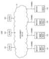
도 2는 본 발명의 실시예들에 따른 마스터 지능 소자를 포함하는 시스템을 나타내는 블록도이다.FIG. 2 is a block diagram illustrating a system including a master intelligence element according to embodiments of the present invention.
이하, 언급되는 시스템은 여러 가지 반도체 부품들이 하나의 칩에 집적된 시스템 온 칩(SOC)을 포함할 수 있으나, 이에 한정되는 것은 아니다.The system referred to below may include, but is not limited to, a system on a chip (SOC) in which various semiconductor components are integrated into a single chip.
도 2를 참조하면, 시스템(1000)은 복수의 슬레이브(slave) 지능 소자(IP, intellectual property)들(SLAVE1, SLAVE2, SLAVE3)(301, 302, 303), 마스터(master) 지능 소자들(MASTER1, MASTER2, MASTER3, MASTER4)(101, 102, 103, 104) 및 상호접속 장치(interconnect device)(10)를 포함할 수 있다. 마스터 지능 소자는 마스터 장치 또는 리퀘스터(requester)로 칭할 수도 있으며, 슬레이브 지능 소자는 슬레이브 장치 또는 리스판더(responder)로 칭할 수도 있다. 상호접속 장치는 페브릭(fabric)으로 칭할 수도 있다.Referring to FIG. 2, a system (1000) may include a plurality of slave intellectual properties (IPs) (SLAVE1, SLAVE2, SLAVE3) (301, 302, 303), master intellectual properties (MASTER1, MASTER2, MASTER3, MASTER4) (101, 102, 103, 104), and an interconnect device (10). The master intellectual property may be referred to as a master device or a requester, and the slave intellectual property may be referred to as a slave device or a responder. The interconnect device may be referred to as a fabric.
복수의 마스터 지능 소자들(101, 102, 103, 104)은 적어도 하나의 슬레이브 지능 소자(301, 302, 303)에게 서비스를 요구하기 위한 리퀘스트들을 각각 발생한다.A plurality of master intelligent elements (101, 102, 103, 104) each generate requests to request services from at least one slave intelligent element (301, 302, 303).
복수의 슬레이브 지능 소자들(301, 302, 303) 및 복수의 마스터 지능 소자들(101, 102, 103, 104)은 각각의 채널(channel)을 통하여 상호접속 장치(10)에 연결된다.A plurality of slave intelligent elements (301, 302, 303) and a plurality of master intelligent elements (101, 102, 103, 104) are connected to an interconnection device (10) through each channel.
상호접속 장치(10)는 각각의 채널들을 통하여 복수의 마스터 지능 소자들(101, 102, 103, 104) 및 복수의 슬레이브 지능 소자들(301, 302, 303)에 연결되고 복수의 마스터 지능 소자들(101, 102, 103, 104) 및 복수의 슬레이브 지능 소자들(301, 302, 303)의 리퀘스트 플로우를 제어할 수 있다. 예를 들어, 상호접속 장치(10)는 상기 리퀘스트들의 긴급한 정도를 나타내는 우선순위 정보들에 기초하여 상기 리퀘스트들의 중재 동작을 수행할 수 있다.The interconnection device (10) is connected to a plurality of master intelligent elements (101, 102, 103, 104) and a plurality of slave intelligent elements (301, 302, 303) through respective channels, and can control the request flow of the plurality of master intelligent elements (101, 102, 103, 104) and the plurality of slave intelligent elements (301, 302, 303). For example, the interconnection device (10) can perform an arbitration operation of the requests based on priority information indicating the degree of urgency of the requests.
도 2에 도시된 마스터 지능 소자들 및 슬레이브 지능 소자들의 개수는 다양하게 변경될 수 있고, 마스터 지능 소자의 동작 특성에 따라서, 마스터 지능 소자들은 서로 다른 구성을 가질 수 있으며, 일부 마스터 지능 소자 및 일부 슬레이브 지능 소자는 생략될 수도 있다.The number of master intelligence elements and slave intelligence elements illustrated in FIG. 2 may vary, and depending on the operating characteristics of the master intelligence elements, the master intelligence elements may have different configurations, and some master intelligence elements and some slave intelligence elements may be omitted.
복수의 마스터 지능 소자들(101, 102, 103, 104) 중 적어도 하나의 마스터 지능 소자는 서비스 수준 모니터 및 리퀘스트 제어 회로를 포함할 수 있다. 도 2에는 제1 마스터 지능 소자(101)는 제1 서비스 수준 모니터(MON1) 및 제1 리퀘스트 제어 회로(RCC1)를 포함하고, 제2 마스터 지능 소자(102)는 제2 서비스 수준 모니터(MON2) 및 제2 리퀘스트 제어 회로(RCC2)를 포함하고, 제3 마스터 지능 소자(103)는 제3 서비스 수준 모니터(MON3) 및 제3 리퀘스트 제어 회로(RCC3)를 포함하는 예가 도시되어 있다. 반면에 적어도 하나의 마스터 지능 소자는, 예를 들어, 제4 마스터 지능 소자(104)는 제4 리퀘스트 제어 회로(RCC4)를 포함하고 서비스 수준 모니터는 포함하지 않을 수 있다.At least one master intelligence element among the plurality of master intelligence elements (101, 102, 103, 104) may include a service level monitor and a request control circuit. FIG. 2 illustrates an example in which a first master intelligence element (101) includes a first service level monitor (MON1) and a first request control circuit (RCC1), a second master intelligence element (102) includes a second service level monitor (MON2) and a second request control circuit (RCC2), and a third master intelligence element (103) includes a third service level monitor (MON3) and a third request control circuit (RCC3). On the other hand, at least one master intelligence element, for example, a fourth master intelligence element (104) may include a fourth request control circuit (RCC4) and may not include a service level monitor.
각각의 서비스 수준 모니터(MONi)(i=1,2,3)는 상응하는 마스터 지능 소자의 상기 리퀘스트들에 대한 서비스 수준을 실시간으로 측정하여 측정 서비스 수준을 제공한다.Each service level monitor (MONi) (i=1,2,3) measures the service level of the corresponding master intelligent element's requests in real time and provides a measured service level.
실시예들에 따라서, 각각의 서비스 수준 모니터(MONi)는 상응하는 마스터 지능 소자가 슬레이브 마스터 지능 소자에 대하여 서비스를 요청한 시점부터 상기 요청한 서비스가 완료되는 시점까지의 시간에 상응하는 레이턴시를 측정한 측정 레이턴시 및 상응하는 마스터 지능 소자에게 단위 시간 동안 전송되거나 서비스되는 데이터의 양에 상응하는 대역폭을 측정한 측정 대역폭 중 적어도 하나를 상기 측정 서비스 수준으로서 제공할 수 있다.According to embodiments, each service level monitor (MONi) may provide at least one of a measured latency corresponding to the time from when a corresponding master intelligent element requests a service to a slave master intelligent element to when the requested service is completed, and a measured bandwidth corresponding to the amount of data transmitted or serviced per unit time to the corresponding master intelligent element, as the measured service level.
각각의 리퀘스트 제어 회로(RCCi)는 상기 측정 서비스 수준에 기초하여 자신의 전력 레벨을 제어한다. 일 실시예에서, 각각의 리퀘스트 제어 회로(RCCi)는 상응하는 마스터 지능 소자가 발행할 수 있는 아웃스탠딩 리퀘스트들의 최대 개수를 변경하는 방식으로 전력 레벨을 제어할 수 있다.Each request control circuit (RCCi) controls its power level based on the measured service level. In one embodiment, each request control circuit (RCCi) can control its power level by varying the maximum number of outstanding requests that the corresponding master intelligent element can issue.
이와 같이, 본 발명의 실시예들에 따른 마스터 지능 소자는 측정 서비스 수준에 따라서 적응적으로 리퀘스트 제어 회로의 전력 레벨을 제어함으로써 마스터 지능 소자의 성능 저하를 방지하면서 상기 마스터 지능 소자 및 상기 마스터 지능 소자를 포함하는 시스템의 전력 소모를 감소할 수 있다.In this way, the master intelligent element according to embodiments of the present invention can reduce power consumption of the master intelligent element and a system including the master intelligent element while preventing performance degradation of the master intelligent element by adaptively controlling the power level of the request control circuit according to the measurement service level.
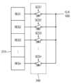
도 3은 본 발명의 실시예들에 따른 마스터 지능 소자를 나타내는 블록도이다.FIG. 3 is a block diagram illustrating a master intelligence element according to embodiments of the present invention.
도 3을 참조하면, 마스터 지능 소자(100)는 내부 회로(200), 리퀘스트 제어 회로(300) 및 서비스 수준 모니터(MON)(500)를 포함할 수 있다.Referring to FIG. 3, the master intelligence element (100) may include an internal circuit (200), a request control circuit (300), and a service level monitor (MON) (500).
내부 회로(200)는 마스터 지능 소자(100)의 고유 기능에 상응하는 다양한 구성을 가질 수 있다. 서비스 수준 모니터(500)는 마스터 지능 소자(100)의 리퀘스트들에 대한 서비스 수준을 실시간으로 측정하여 측정 서비스 수준(MSL)을 제공할 수 있다. 리퀘스트 제어 회로(300)는 상호접속 장치(10)에 연결된 채널을 통하여 리퀘스트(REQ)를 발행하고(issue) 리퀘스트(REQ)에 대한 응답(RSP)을 수신할 수 있다.The internal circuit (200) may have various configurations corresponding to the unique functions of the master intelligent element (100). The service level monitor (500) may measure the service level for requests of the master intelligent element (100) in real time and provide a measured service level (MSL). The request control circuit (300) may issue a request (REQ) and receive a response (RSP) to the request (REQ) through a channel connected to the interconnection device (10).
리퀘스트 제어 회로(300)는, 리퀘스트 큐(310), 스케쥴러(320), 리소스 콘트롤러(RSCON)(330) 및 게이트 회로(GTC)(340)를 포함할 수 있다.The request control circuit (300) may include a request queue (310), a scheduler (320), a resource controller (RSCON) (330), and a gate circuit (GTC) (340).
리퀘스트 큐(310)는 리퀘스트들을 각각 저장하기 위한 복수의 리퀘스트 저장 유닛들(REG1~REGn)을 포함할 수 있다. 다중 아웃스탠딩 트랜잭션(multiple outstanding transactions) 또는 다중 아웃스탠딩 리퀘스트(multiple outstanding requests)를 지원하는 프로토콜이 채용되는 경우, 마스터 지능 소자는 적어도 하나의 리퀘스트 큐(310)를 포함할 수 있다. 리퀘스트 큐(310)는 마스터 지능 소자들로부터 발행될 예정인 리퀘스트 및 이미 발행되었으나(issued) 아직 완료되지 않은 복수의 리퀘스트들을 저장한다.The request queue (310) may include a plurality of request storage units (REG1 to REGn) for storing requests, respectively. When a protocol supporting multiple outstanding transactions or multiple outstanding requests is adopted, the master intelligent element may include at least one request queue (310). The request queue (310) stores requests to be issued from the master intelligent elements and a plurality of requests that have already been issued but not yet completed.
스케쥴러(320)는 리퀘스트 큐(310)에 저장된 리퀘스트들의 각각의 우선순위들에 기초하여 상기 저장된 리퀘스트들에 대한 서비스 순서를 결정할 수 있다. 결정된 서비스 순서에 따라서 리퀘스트들이 순차적으로 상호접속 장치(10)에 전달될 수 있다.The scheduler (320) can determine the service order for the stored requests based on the respective priorities of the requests stored in the request queue (310). The requests can be sequentially delivered to the interconnection device (10) according to the determined service order.
리소스 콘트롤러(330)는 측정 서비스 수준(MSL)에 기초하여 마스터 지능 소자(100)가 발행할 수 있는 아웃스탠딩 리퀘스트들의 최대 개수(MXN)를 결정할 수 있다. 일 실시예에서, 리소스 콘트롤러(330)는 아웃스탠딩 리퀘스트들의 최대 개수(MXN)에 기초하여 게이트 제어 신호(GCS)를 발생할 수 있다. 게이트 제어 신호(GCS)는 도 4를 참조하여 후술하는 바와 같이 복수의 스위치 제어 신호들(GCS1~GCSn)을 포함할 수 있다. 아웃스탠딩 리퀘스트들의 최대 개수(MXN)는 스케쥴러(320)에 제공되고, 스케쥴러(320)는 아웃스탠딩 리퀘스트들의 최대 개수(MXN)에 상응하는 리퀘스트들의 저장 및 발행 순서를 제어할 수 있다.The resource controller (330) can determine a maximum number (MXN) of outstanding requests that the master intelligent element (100) can issue based on a measured service level (MSL). In one embodiment, the resource controller (330) can generate a gate control signal (GCS) based on the maximum number (MXN) of outstanding requests. The gate control signal (GCS) can include a plurality of switch control signals (GCS1 to GCSn) as described below with reference to FIG. 4. The maximum number (MXN) of outstanding requests is provided to the scheduler (320), and the scheduler (320) can control the storage and issuance order of requests corresponding to the maximum number (MXN) of outstanding requests.
게이트 회로(340)는 게이트 제어 신호(GCS)에 기초하여 복수의 리퀘스트 저장 유닛들(REG1~REGn)에 각각 공급되는 동작 클록 신호(CLK) 및 전원 전압(VDD)을 제어할 수 있다.The gate circuit (340) can control the operation clock signal (CLK) and power supply voltage (VDD) supplied to each of the plurality of request storage units (REG1 to REGn) based on a gate control signal (GCS).
도 4는 본 발명의 실시예들에 따른 마스터 지능 소자의 전력 레벨 제어의 일 실시예를 설명하기 위한 도면이다.FIG. 4 is a diagram for explaining one embodiment of power level control of a master intelligent element according to embodiments of the present invention.
도 4를 참조하면, 게이트 회로(340)는 리퀘스트 큐(310)에 포함되는 복수의 리퀘스트 저장 유닛들(REG1~REGn)에 공급되는 동작 클록 신호(CLK) 및 전원 전압(VDD)을 각각 게이팅하는 복수의 스위치들(SW1~SWn)을 포함할 수 있다.Referring to FIG. 4, the gate circuit (340) may include a plurality of switches (SW1 to SWn) that gate the operation clock signal (CLK) and the power supply voltage (VDD) supplied to a plurality of request storage units (REG1 to REGn) included in the request queue (310), respectively.
도 3 및 4를 참조하면, 리소스 콘트롤러(330)는 복수의 스위치들(SW1~SWn)의 스위칭 동작을 각각 제어하기 위한 복수의 스위치 제어 신호들(GCS1~GCSn)을 발생할 수 있고, 복수의 스위치들(SW1~SWn)은 복수의 스위치 제어 신호들(GCS1~GCSn)의 각각의 활성화 또는 비활성화에 따라서 턴온 또는 턴오프될 수 있다.Referring to FIGS. 3 and 4, the resource controller (330) can generate a plurality of switch control signals (GCS1 to GCSn) for respectively controlling switching operations of a plurality of switches (SW1 to SWn), and the plurality of switches (SW1 to SWn) can be turned on or off according to activation or deactivation of each of the plurality of switch control signals (GCS1 to GCSn).
리소스 콘트롤러(330)는 서비스 수준 모니터(500)로부터 제공되는 측정 서비스 수준(MSL)에 기초하여 복수의 스위치 제어 신호들(GCS1~GCSn) 중에서 활성화되는 스위치 제어 신호들의 개수를 변경할 수 있다.The resource controller (330) can change the number of switch control signals activated among the plurality of switch control signals (GCS1 to GCSn) based on the measured service level (MSL) provided from the service level monitor (500).
복수의 스위치 제어 신호들(GCS1~GCSn) 중 각각의 스위치 제어 신호(GCSi)(i=1~n)가 활성화되는 경우 상응하는 스위치(SWi)가 턴온되어 상응하는 리퀘스트 저장 유닛(REGi)에 동작 클록 신호(CLK) 및 전원 전압(VDD)이 공급되어 상응하는 리퀘스트 저장 유닛(REGi)이 인에이블될 수 있다. 반면에, 각각의 스위치 제어 신호(GCSi)가 비활성화되는 경우 상응하는 스위치(SWi)가 턴오프되어 상응하는 리퀘스트 저장 유닛(REGi)에 공급되는 동작 클록 신호(CLK) 및 전원 전압(VDD)이 차단되어 상응하는 리퀘스트 저장 유닛(REGi)이 디스에이블될 수 있다.When each switch control signal (GCSi) (i=1 to n) among the plurality of switch control signals (GCS1 to GCSn) is activated, the corresponding switch (SWi) is turned on so that the operation clock signal (CLK) and the power supply voltage (VDD) are supplied to the corresponding request storage unit (REGi), so that the corresponding request storage unit (REGi) can be enabled. On the other hand, when each switch control signal (GCSi) is deactivated, the corresponding switch (SWi) is turned off so that the operation clock signal (CLK) and the power supply voltage (VDD) supplied to the corresponding request storage unit (REGi) are blocked, so that the corresponding request storage unit (REGi) can be disabled.
리소스 콘트롤러(330)는, 측정 서비스 수준(MSL)이 증가할수록 복수의 리퀘스트 저장 유닛들(REG1~REGn) 중에서 동작 클록 신호(CLK) 및 전원 전압(VDD)을 공급받는 리퀘스트 저장 유닛들의 개수를 감소하도록 활성화되는 스위치 제어 신호들의 개수를 감소할 수 있다. 다시 말해, 측정 서비스 수준(MSL)이 증가할수록 복수의 리퀘스트 저장 유닛들(REG1~REGn) 중에서 인에이블되는 리퀘스트 저장 유닛들의 개수를 감소할 수 있다. 결과적으로 측정 서비스 수준(MSL)이 증가할수록 아웃스탠딩 리퀘스트들의 최대 개수(MXN)를 감소할 수 있다.The resource controller (330) can reduce the number of switch control signals that are activated to reduce the number of request storage units supplied with the operating clock signal (CLK) and the power supply voltage (VDD) among the plurality of request storage units (REG1 to REGn) as the measurement service level (MSL) increases. In other words, the number of enabled request storage units among the plurality of request storage units (REG1 to REGn) can be reduced as the measurement service level (MSL) increases. As a result, the maximum number (MXN) of outstanding requests can be reduced as the measurement service level (MSL) increases.
도 5a 및 5b는 본 발명의 실시예들에 따른 마스터 지능 소자의 전력 레벨 제어를 설명하기 위한 도면들이다.FIGS. 5A and 5B are diagrams for explaining power level control of a master intelligent element according to embodiments of the present invention.
도 5a를 참조하면, 본 발명의 실시예들에 따라서 측정 서비스 수준(MSL)이 증가할수록 복수의 리퀘스트 저장 유닛들(REG1~REGn) 중에서 인에이블되는 리퀘스트 저장 유닛들의 개수(NEQ)를 감소할 수 있다.Referring to FIG. 5a, according to embodiments of the present invention, as the measured service level (MSL) increases, the number (NEQ) of enabled request storage units among a plurality of request storage units (REG1 to REGn) can be reduced.
도 5b에는 제1 내지 제4 마스터 지능 소자들(MST1~MST4)이 제1 내지 제4 슬레이브 지능 소자들(SLV1~SLV4)과 각각 트랜잭션을 수행하는 제1 내지 제4 경우들(CS1~CS4)이 도시되어 있다. 각각의 마스터 지능 소자는 각각의 슬레이브 지능 소자에게 서비스에 대한 리퀘스트(REQ)를 발행하고 상응하는 슬레이브 지능 소자로부터 상기 서비스에 대한 응답(RSP)을 수신한다.FIG. 5b illustrates first to fourth cases (CS1 to CS4) in which first to fourth master intelligent elements (MST1 to MST4) perform transactions with first to fourth slave intelligent elements (SLV1 to SLV4), respectively. Each master intelligent element issues a request for service (REQ) to each slave intelligent element and receives a response (RSP) to the service from the corresponding slave intelligent element.
제1 내지 제4 마스터 지능 소자들(MST1~MST4)은 제1 내지 제4 리퀘스트 큐들(RQ1~RQ4)을 각각 포함할 수 있다. 제1 내지 제4 리퀘스트 큐들(RQ1~RQ4)의 각각은 복수의 리퀘스트 저장 유닛들을 포함한다. 도 5b에는 디스에이블되는 리퀘스트 저장 유닛들이 빗금으로 표시되어(hatched) 있다.The first to fourth master intelligent elements (MST1 to MST4) may each include first to fourth request queues (RQ1 to RQ4). Each of the first to fourth request queues (RQ1 to RQ4) includes a plurality of request storage units. In Fig. 5b, the disabled request storage units are hatched.
상호접속 장치(10)는 스위치 회로(SWT), 컨버터(CNV)와 같은 다양한 구성요소들을 포함할 수 있고, 트랜잭션이 이러한 구성요소들을 경유하는 경우 레이턴시가 증가하게 된다. 본 발명의 실시예들에 따라서, 레이턴시가 증가할수록, 즉 측정 서비스 수준(MSL)이 감소할수록, 레이턴시를 감소하기 위해 인이에블되는 리퀘스트 저장 유닛들의 개수(NEQ)를 증가할 수 있다. 반대로 레이턴시가 감소할수록, 즉 측정 서비스 수준(MSL)이 증가할수록, 레이턴시를 증가시키고 전력 소모를 감소하기 위해 인이에블되는 리퀘스트 저장 유닛들의 개수(NEQ)를 감소할 수 있다.The interconnection device (10) may include various components such as a switch circuit (SWT) and a converter (CNV), and when a transaction passes through these components, latency increases. According to embodiments of the present invention, as the latency increases, that is, as the measured service level (MSL) decreases, the number (NEQ) of request storage units enabled to reduce the latency may increase. Conversely, as the latency decreases, that is, as the measured service level (MSL) increases, the number (NEQ) of request storage units enabled to increase the latency and reduce power consumption may decrease.
제1 내지 제3 마스터 지능 소자들(MST1~MST3)은 본 발명의 실시예들에 따른 제어 방법을 수행하는 지능 소자들에 해당한다. 제1 경우(CS1)에는 중간에 경유하는 구성 요소가 없으므로 레이턴시가 상대적으로 작으므로 인에이블되는 리퀘스트 저장 유닛들의 개수가 상대적으로 작을 수 있다. 제2 경우(CS2)는 제1 경우(CS1)보다 레이턴시가 증가하므로, 제1 경우(CS1)보다 제2 경우(CS2)에 인에이블되는 리퀘스트 저장 유닛들의 개수가 증가한다. 마찬가지로 제3 경우(CS3)는 제2 경우(CS2)보다 레이턴시가 증가하므로, 제2 경우(CS2)보다 제3 경우(CS3)에 인에이블되는 리퀘스트 저장 유닛들의 개수가 증가한다.The first to third master intelligent elements (MST1 to MST3) correspond to intelligent elements that perform the control method according to embodiments of the present invention. In the first case (CS1), since there is no intermediate component, the latency is relatively small, and thus the number of enabled request storage units can be relatively small. In the second case (CS2), the latency increases more than in the first case (CS1), and thus the number of enabled request storage units increases more in the second case (CS2) than in the first case (CS1). Similarly, in the third case (CS3), the latency increases more than in the second case (CS2), and thus the number of enabled request storage units increases more in the third case (CS3) than in the second case (CS2).
제4 마스터 지능 소자(MST4)는 본 발명의 실시예들에 따른 제어 방법을 채용하지 않은 지능 소자에 해당한다. 제4 경우(CS4)에는 제1 경우(CS1)와 동일한 레이턴시를 갖지만 레이턴시에 관계없이 모든 리퀘스트 저장 유닛들이 인에이블된다. 따라서, 레이턴시가 필요 이상 감소함으로써 소모 전력이 불필요하게 증가하게 된다.The fourth master intelligent element (MST4) corresponds to an intelligent element that does not employ the control method according to embodiments of the present invention. In the fourth case (CS4), the same latency as in the first case (CS1) is present, but all request storage units are enabled regardless of the latency. Therefore, the latency is reduced more than necessary, which unnecessarily increases power consumption.
이와 같이, 본 발명의 실시예들에 따른 마스터 지능 소자 및 상기 마스터 지능 소자의 제어 방법은 측정 서비스 수준에 따라서 적응적으로 리퀘스트 제어 회로의 전력 레벨을 제어함으로써 마스터 지능 소자의 성능 저하를 방지하면서 상기 마스터 지능 소자 및 상기 마스터 지능 소자를 포함하는 시스템의 전력 소모를 감소할 수 있다.In this way, the master intelligent element and the control method of the master intelligent element according to embodiments of the present invention can reduce power consumption of the master intelligent element and a system including the master intelligent element while preventing performance degradation of the master intelligent element by adaptively controlling the power level of the request control circuit according to the measurement service level.
도 6a 및 6b는 측정 서비스 수준 및 다양한 서비스 수준 사이의 관계를 나타내는 도면들이다.Figures 6a and 6b are diagrams showing measurement service levels and relationships between various service levels.
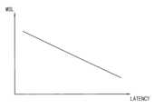
도 6a에 도시된 바와 같이 레이턴시가 증가할수록 측정 서비스 수준(MSL)이 감소한다. 레이턴시가 크다는 것은 서비스가 적시에 제공되지 못하는 것을 의미하며, 따라서, 측정 서비스 수준(MSL)과 레이턴시는 반비례하는 관계에 있다.As shown in Figure 6a, as latency increases, the measured service level (MSL) decreases. A large latency means that the service is not provided in a timely manner, and therefore, the measured service level (MSL) and latency are inversely proportional.
한편, 도 6b에 도시된 바와 같이 대역폭이 증가할수록 측정 서비스 수준(MSL)이 증가한다. 대역폭이 크다는 것은 서비스되는 데이터의 양이 충분하다는 것을 의미하며, 따라서, 측정 서비스 수준(MSL)과 대역폭은 비례하는 관계에 있다.Meanwhile, as shown in Fig. 6b, as the bandwidth increases, the measured service level (MSL) increases. A large bandwidth means that the amount of data being served is sufficient, and therefore, the measured service level (MSL) and the bandwidth are proportional.
도 7은 리퀘스트 큐에 저장되는 리퀘스트의 포맷의 일 예를 나타내는 도면이다.Figure 7 is a diagram showing an example of the format of a request stored in a request queue.
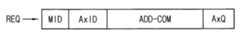
도 7을 참조하면, 리퀘스트 큐에 저장되는 리퀘스트들(REQ)은 리퀘스트(REQ)를 발생한 마스터 지능 소자를 나타내는 마스터 식별자(MID), 복수의 리퀘스트들을 구별하기 위한 리퀘스트 식별자(AxID), 리퀘스트(REQ)의 내용을 나타내는 어드레스-코맨드(ADD-COM) 및 리퀘스트(REQ)의 우선순위(AxQ)를 포함할 수 있다. 우선순위(AxQ)는 상호접속 장치(10) 내에서 전달되어 리퀘스트들의 중재를 위한 정보로서 이용될 수 있다.Referring to FIG. 7, requests (REQ) stored in a request queue may include a master identifier (MID) indicating a master intelligent element that has generated the request (REQ), a request identifier (AxID) for distinguishing multiple requests, an address-command (ADD-COM) indicating the contents of the request (REQ), and a priority (AxQ) of the request (REQ). The priority (AxQ) may be transmitted within the interconnection device (10) and used as information for arbitration of requests.
도 8은 본 발명의 실시예들에 따른 마스터 지능 소자에 포함되는 서비스 수준 모니터의 일 실시예를 나타내는 블록도이다. 도 8에는 현재 레이턴시를 전술한 측정 서비스 수준(MSL)으로서 제공하는 레이턴시 검출기가 도시되어 있다.FIG. 8 is a block diagram illustrating one embodiment of a service level monitor included in a master intelligent element according to embodiments of the present invention. FIG. 8 illustrates a latency detector that provides the current latency as the aforementioned measured service level (MSL).
도 8을 참조하면, 레이턴시 검출기(540)는 제1 플립플롭(flip-flop)(FF1)(541), 제2 플립플롭(FF2)(542), 카운터(counter)(543), 제1 래치(LATCH1)(544), 제2 래치(LATCH2)(545), 계산기(546), 제1 논리 게이트(548) 및 제2 논리 게이트(549)를 포함할 수 있다.Referring to FIG. 8, the latency detector (540) may include a first flip-flop (FF1) (541), a second flip-flop (FF2) (542), a counter (543), a first latch (LATCH1) (544), a second latch (LATCH2) (545), a calculator (546), a first logic gate (548), and a second logic gate (549).
예를 들어, 제1 논리 게이트(548)는 논리곱 게이트(AND 게이트)로 구현될 수 있으며, 제1 논리 게이트(548)는 리퀘스트 밸리드 신호(ARVALID) 및 리퀘스트 레디 신호(ARREADY)를 논리곱 연산한 결과를 출력한다. 제1 플립플롭(541)의 데이터 단자(D)에는 제1 논리 게이트(548)의 출력 신호가 입력되고 클록 단자(C)에는 글로벌 클록 신호(ACLK)가 입력된다. 제1 플립플롭(541)은 글로벌 클록 신호(ACLK)의 상승 에지에 응답하여 제1 논리 게이트(548)의 출력 신호를 샘플링하여 글로벌 클록 신호(ACLK)의 상승 에지에 동기된 신호(SS1)를 출력 단자(Q)를 통하여 출력한다.For example, the first logic gate (548) can be implemented as an AND gate, and the first logic gate (548) outputs the result of an AND operation on a request validated signal (ARVALID) and a request ready signal (ARREADY). An output signal of the first logic gate (548) is input to a data terminal (D) of the first flip-flop (541), and a global clock signal (ACLK) is input to a clock terminal (C). The first flip-flop (541) samples the output signal of the first logic gate (548) in response to a rising edge of the global clock signal (ACLK) and outputs a signal (SS1) synchronized with the rising edge of the global clock signal (ACLK) through the output terminal (Q).
예를 들어, 제2 논리 게이트(549)는 논리곱 게이트(AND 게이트)로 구현될 수 있으며, 제2 논리 게이트(549)는 서비스 밸리드 신호(RVALID), 서비스 레디 신호(RREADY) 및 서비스 완료 신호(RLAST)를 논리곱 연산한 결과를 출력한다. 제2 플립플롭(542)의 데이터 단자(D)에는 제2 논리 게이트(549)의 출력 신호가 입력되고 클록 단자(C)에는 글로벌 클록 신호(ACLK)가 입력된다. 제2 플립플롭(542)은 글로벌 클록 신호(ACLK)의 상승 에지에 응답하여 제2 논리 게이트(549)의 출력 신호를 샘플링하여 글로벌 클록 신호(ACLK)의 상승 에지에 동기된 신호(SS2)를 출력 단자(Q)를 통하여 출력한다.For example, the second logic gate (549) can be implemented as a AND gate, and the second logic gate (549) outputs the result of an AND operation on a service valid signal (RVALID), a service ready signal (RREADY), and a service complete signal (RLAST). An output signal of the second logic gate (549) is input to a data terminal (D) of the second flip-flop (542), and a global clock signal (ACLK) is input to a clock terminal (C). The second flip-flop (542) samples the output signal of the second logic gate (549) in response to a rising edge of the global clock signal (ACLK) and outputs a signal (SS2) synchronized with the rising edge of the global clock signal (ACLK) through an output terminal (Q).
카운터(543)는 글로벌 클록 신호(ACLK)의 사이클 횟수를 카운팅하여 카운트 신호(CNT)를 제공한다.The counter (543) counts the number of cycles of the global clock signal (ACLK) and provides a count signal (CNT).
제1 래치(544)는 제1 플립플롭(541)의 출력 신호(SS1)의 상승 에지에 응답하여 카운트 신호(CNT)를 래치하고 시작 카운트 신호(CNT1)를 제공한다. 또한 제1 래치(544)는 리퀘스트 신호들(ARVALID, ARREADY)과 연계된 제1 식별 신호(ARID)를 수신하여 제1 식별 코드(ID1)를 제공한다.The first latch (544) latches a count signal (CNT) in response to a rising edge of an output signal (SS1) of the first flip-flop (541) and provides a start count signal (CNT1). In addition, the first latch (544) receives a first identification signal (ARID) linked to request signals (ARVALID, ARREADY) and provides a first identification code (ID1).
제2 래치(545)는 제2 플립플롭(542)의 출력 신호(SS2)의 상승 에지에 응답하여 카운트 신호(CNT)를 래치하고 완료 카운트 신호(CNT2)를 제공한다. 또한 제2 래치(545)는 서비스 신호들(RVALID, RREADY, RLAST)과 연계된 제2 식별 신호(BID)를 수신하여 제2 식별 코드(ID2)를 제공한다.The second latch (545) latches a count signal (CNT) in response to a rising edge of an output signal (SS2) of the second flip-flop (542) and provides a completion count signal (CNT2). In addition, the second latch (545) receives a second identification signal (BID) linked to service signals (RVALID, RREADY, RLAST) and provides a second identification code (ID2).
계산기(546)는 시작 카운트 신호(CNT1) 및 완료 카운트 신호(CNT2)에 기초하여 현재 레이턴시(CLAT)를 발생한다. 시스템(1000)이 마스터 지능 소자들, 상호접속 장치 및 슬레이브 지능 소자들 사이의 다중 아웃스탠딩 트랜잭션(multiple outstanding transactions)을 지원하는 프로토콜을 채용하는 경우, 동일한 트랜잭션에 상응하는 리퀘스트 신호들(ARVALID, ARREADY)과 서비스 신호들(RVALID, RREADY, RLAST)을 구별하기 위하여 식별 신호들(ARID, BID)이 이용될 수 있다.The calculator (546) generates the current latency (CLAT) based on the start count signal (CNT1) and the completion count signal (CNT2). When the system (1000) employs a protocol that supports multiple outstanding transactions between master intelligent elements, interconnection devices, and slave intelligent elements, identification signals (ARID, BID) may be used to distinguish between request signals (ARVALID, ARREADY) and service signals (RVALID, RREADY, RLAST) corresponding to the same transaction.
계산기(546)는 제1 카운트 신호(CNT1) 및 제1 식별 코드(ID1)가 입력될 때마다 매핑 테이블(547)을 갱신하여 제1 식별 신호(ARID)에 상응하는 제1 식별 코드(ID1)의 값(ID11, ID12, ID13)과 이에 상응하는 제1 카운트 신호(CNT1)의 값들(C1, C2, C3)을 저장한다. 계산기(546)는 제2 카운트 신호(CNT2) 및 제2 식별 코드(ID2)가 입력되면 매핑 테이블(547)로부터 입력된 제2 카운트 신호(CNT2)에 상응하는 리퀘스트 요청 시점을 나타내는 카운트 값(C1, C2 또는 C3)을 추출한다.Whenever a first count signal (CNT1) and a first identification code (ID1) are input, the calculator (546) updates the mapping table (547) to store the values (ID11, ID12, ID13) of the first identification code (ID1) corresponding to the first identification signal (ARID) and the values (C1, C2, C3) of the first count signal (CNT1) corresponding thereto. When a second count signal (CNT2) and a second identification code (ID2) are input, the calculator (546) extracts a count value (C1, C2 or C3) indicating a request request time point corresponding to the input second count signal (CNT2) from the mapping table (547).
계산기(546)는 입력되는 제2 카운트 신호(CNT2)의 리퀘스트 완료 시점을 나타내는 카운트 값과 상기 추출된 카운트 값의 차이를 계산하여 현재 레이턴시(CLAT)를 발생할 수 있다.The calculator (546) can generate the current latency (CLAT) by calculating the difference between the count value indicating the request completion time of the input second count signal (CNT2) and the extracted count value.
이와 같이 구해진 현재 레이턴시(CLAT)를 본 발명의 실시예들에 따른 마스터 지능 소자의 제어 방법을 위한 측정 서비스 수준(MSL)으로서 이용할 수 있다.The current latency (CLAT) obtained in this manner can be used as a measurement service level (MSL) for a control method of a master intelligent element according to embodiments of the present invention.
도 9는 본 발명의 실시예들에 따른 시스템에 의해 수행되는 트랜잭션의 일 예 및 도 8의 레이턴시 검출기에 의해 검출되는 현재 레이턴시를 설명하기 위한 파형도이다.FIG. 9 is a waveform diagram illustrating an example of a transaction performed by a system according to embodiments of the present invention and a current latency detected by the latency detector of FIG. 8.
도 9에는 설명의 편의를 위하여 AXI(advanced extensible interface) 프로토콜에 따른 독출 트랜잭션의 예가 도시되어 있다. AXI 프로토콜은 밸리드 신호(ARVALID, RVALID) 및 레디 신호(ARREADY, RREADY)를 이용하는 핸드쉐이크 방식(handshake mechanism)을 채택하고 있다.For convenience of explanation, Fig. 9 illustrates an example of a read transaction according to the advanced extensible interface (AXI) protocol. The AXI protocol adopts a handshake mechanism that uses valid signals (ARVALID, RVALID) and ready signals (ARREADY, RREADY).
핸드쉐이크 방식에 따르면, 마스터 인터페이스 및 슬레이브 인터페이스의 일측에서는 신호 전송시 밸리드 신호를 활성화하고 타측에서는 수신 준비가 되었을 때 레디 신호를 활성화한다. 마스터 인터페이스 및 슬레이브 인터페이스의 양자 모두에서 글로벌 클록 신호(ACLK)의 상승 에지에 동기하여 전송 신호의 샘플링이 수행된다. 따라서 밸리드 신호 및 상응하는 레디 신호가 글로벌 클록 신호(ACLK)의 상승 에지에서 모두 활성화될 때만 유효한 신호 전송이 이루어진다.According to the handshake method, one side of the master interface and the slave interface activates the valid signal when transmitting a signal, and the other side activates the ready signal when ready to receive. Sampling of the transmission signal is performed in synchronization with the rising edge of the global clock signal (ACLK) in both the master interface and the slave interface. Therefore, a valid signal transmission is performed only when both the valid signal and the corresponding ready signal are activated at the rising edge of the global clock signal (ACLK).
도 9에 도시된 바와 같이, 마스터 인터페이스에 상응하는 마스터 지능 소자(100)는 신호 전송시 리퀘스트 밸리드 신호(ARVALID)를 활성화하고 슬레이브 인터페이스에 상응하는 상호접속 장치(10)는 수신 준비가 되었을 때 리퀘스트 레디 신호(ARREADY)를 활성화한다. 마찬가지로 상호접속 장치(10)는 신호 전송시 서비스 밸리드 신호(RVALID)를 활성화하고 마스터 지능 소자(100)는 수신 준비가 되었을 때 서비스 레디 신호(RREADY)를 활성화한다.As illustrated in FIG. 9, the master intelligent element (100) corresponding to the master interface activates the request valid signal (ARVALID) when transmitting a signal, and the interconnection device (10) corresponding to the slave interface activates the request ready signal (ARREADY) when ready to receive. Similarly, the interconnection device (10) activates the service valid signal (RVALID) when transmitting a signal, and the master intelligent element (100) activates the service ready signal (RREADY) when ready to receive.
도 9에는 글로벌 클록 신호(ACLK)의 상승 에지를 나타내는 시점들이 T0~T13으로 표시되어 있다. 마스터 인터페이스, 예를 들어, 마스터 지능 소자(100)는 독출 리퀘스트 신호(ARADDR)를 슬레이브 인터페이스, 예를 들어, 상호접속 장치(10)로 전송하는 것과 함께 리퀘스트 요청 신호에 상응하는 독출 밸리드 신호(ARVALID)를 활성화한다. 시간 T2에서 밸리드 신호(ARVALID) 및 레디 신호(RREADY)가 모두 활성화되어 독출 리퀘스트 신호(ARADDR)의 전송이 실제로 수행된다. 그러나 마스터 인터페이스의 관점에서는 슬레이브 인터페이스의 레디 신호(RREADY)의 활성화 여부에 관계없이, 즉 실제 신호 전송의 성공 여부와 관계없이 시간 T1을 리퀘스트 요청 시점으로 결정할 수 있다.In Fig. 9, time points indicating rising edges of a global clock signal (ACLK) are indicated as T0 to T13. A master interface, for example, a master intelligent element (100), transmits a read request signal (ARADDR) to a slave interface, for example, an interconnection device (10), and activates a read valid signal (ARVALID) corresponding to the request request signal. At time T2, both the valid signal (ARVALID) and the ready signal (RREADY) are activated, so that transmission of the read request signal (ARADDR) is actually performed. However, from the viewpoint of the master interface, time T1 can be determined as the request request time point regardless of whether the ready signal (RREADY) of the slave interface is activated, that is, regardless of whether actual signal transmission is successful.
상기 독출 리퀘스트에 대한 응신으로서 데이터(D(A0), D(A1), D(A2), D(A3))가 버스트 전송 방식에 의해 상호접속 장치(10)로부터 마스터 지능 소자(100)로 전송된다. 상호접속 장치(10)는 마지막 데이터(D(A3))의 전송과 함께 서비스 완료 신호에 상응하는 RLAST 신호를 활성화하고, 시간 T13이 리퀘스트 완료 시점으로 결정된다.As a response to the above read request, data (D(A0), D(A1), D(A2), D(A3)) are transmitted from the interconnection device (10) to the master intelligent element (100) by a burst transmission method. The interconnection device (10) activates a RLAST signal corresponding to a service completion signal along with the transmission of the last data (D(A3)), and time T13 is determined as the request completion point in time.
이와 같이, 도 8의 레이턴시 검출기(540)는 마스터 지능 소자와 상호접속 장치(10) 사이의 채널 신호 중에서 마스터 지능 소자(100)와 상호접속 장치(10) 사이의 리퀘스트 신호들(ARVALID, ARREADY) 및 서비스 신호들(RVALID, RREADY, RLAST)에 기초하여 현재 레이턴시(CLAT)를 발생할 수 있다.In this way, the latency detector (540) of FIG. 8 can generate the current latency (CLAT) based on the request signals (ARVALID, ARREADY) and service signals (RVALID, RREADY, RLAST) between the master intelligent element (100) and the interconnection device (10) among the channel signals between the master intelligent element and the interconnection device (10).
도 10은 본 발명의 일 실시예에 따른 레이턴시 검출을 위한 축적기 모델을 나타내는 도면이다.FIG. 10 is a diagram illustrating an accumulator model for latency detection according to one embodiment of the present invention.
마스터 지능 소자의 동작 특성에 따라서 마스터 지능 소자의 서비스 수준은 레이턴시(latency)로 표현될 수 있다. 레이턴시는 마스터 지능 소자가 슬레이브 마스터 지능 소자에 대하여 서비스를 요청한 시점부터 상기 요청한 서비스가 완료되는 시점까지의 시간을 나타내며, 예를 들어, 레이턴시는 클록 신호의 사이클 횟수 등으로 표현될 수도 있다.Depending on the operating characteristics of the master intelligent element, the service level of the master intelligent element can be expressed in terms of latency. Latency refers to the time from the time the master intelligent element requests a service from the slave master intelligent element to the time the requested service is completed. For example, latency can also be expressed in terms of the number of cycles of a clock signal.
도 10에는 상기 마스터 지능 소자의 레이턴시 상태가 빗금으로 표시되는 레이턴시 축적기(latency accumulator)가 도시되어 있다. 레이턴시 상태는 현재 레이턴시 레벨(LCL)로 표현될 수 있고, 레이턴시가 증가하면 현재 레이턴시 레벨(LCL)이 증가하고 레이턴시가 감소하면 현재 레이턴시 레벨(LCL)이 감소한다. 현재 레이턴시 레벨(LCL)이 타겟 레이턴시 레벨(예를 들어, LTL1)보다 높은 경우, 레이턴시 감소를 위해 아웃스탠딩 리퀘스트들의 최대 개수(MXN) 또는 인에이블되는 리퀘스트 저장 유닛들의 개수(NEQ)를 증가할 수 있다. 한편, 현재 레이턴시 레벨(LCL)이 타겟 레이턴시 레벨(예를 들어, LTL2)보다 낮은 경우, 레이턴시를 증가하여 소모 전력을 감소하기 위해 아웃스탠딩 리퀘스트들의 최대 개수(MXN) 또는 인에이블되는 리퀘스트 저장 유닛들의 개수(NEQ)를 감소할 수 있다.FIG. 10 illustrates a latency accumulator in which the latency state of the master intelligent element is indicated by hatching. The latency state can be expressed by a current latency level (LCL), and when the latency increases, the current latency level (LCL) increases, and when the latency decreases, the current latency level (LCL) decreases. If the current latency level (LCL) is higher than a target latency level (e.g., LTL1), the maximum number of outstanding requests (MXN) or the number of enabled request storage units (NEQ) can be increased to reduce the latency. On the other hand, if the current latency level (LCL) is lower than the target latency level (e.g., LTL2), the maximum number of outstanding requests (MXN) or the number of enabled request storage units (NEQ) can be decreased to increase the latency and reduce power consumption.
도 11은 도 10의 축적기 모델을 이용하는 서비스 수준 모니터의 일 실시예를 나타내는 블록도이다.FIG. 11 is a block diagram illustrating one embodiment of a service level monitor using the accumulator model of FIG. 10.
도 11을 참조하면, 본 발명의 실시예들에 따른 서비스 수준 모니터는 레이턴시 모니터(500a)로 구현될 수 있다.Referring to FIG. 11, a service level monitor according to embodiments of the present invention can be implemented as a latency monitor (500a).
레이턴시 모니터(latency monitor)(500a)는 상응하는 마스터 지능 소자의 레이턴시를 축적하여 현재 레이턴시 레벨(LCL)을 발생한다. 레이턴시 모니터(500a)는 감산기(subtractor)(SUB)(535), 축적기(accumulator)(ACC)(537) 및 레이턴시 검출기(latency detector)(LATDET)(540)를 포함할 수 있다.A latency monitor (500a) accumulates the latency of a corresponding master intelligent element and generates a current latency level (LCL). The latency monitor (500a) may include a subtractor (SUB) (535), an accumulator (ACC) (537), and a latency detector (LATDET) (540).
레이턴시 검출기(540)는 도 8을 참조하여 설명한 바와 같이 상응하는 마스터 지능 소자와 상호접속 장치(10) 사이의 채널 신호(CHN)에 기초하여 현재 레이턴시(CLAT)를 발생할 수 있다 감산기(535)는 현재 레이턴시(LCL) 및 기준 레이턴시(RLAT)의 차이를 계산하여 레이턴시 변화값(dLAT)을 출력할 수 있다. 축적기(537)는 레이턴시 변화값(dLAT)을 누산하여 현재 레이턴시 레벨(LCL)을 발생할 수 있다.The latency detector (540) can generate a current latency (CLAT) based on a channel signal (CHN) between a corresponding master intelligent element and an interconnection device (10) as described with reference to FIG. 8. The subtractor (535) can calculate a difference between the current latency (LCL) and a reference latency (RLAT) and output a latency change value (dLAT). The accumulator (537) can accumulate the latency change value (dLAT) and generate a current latency level (LCL).
이와 같이 구해진 현재 레이턴시 레벨(LCL)을 본 발명의 실시예들에 따른 마스터 지능 소자의 제어 방법을 위한 측정 서비스 수준(MSL)으로서 이용할 수 있다.The current latency level (LCL) obtained in this manner can be used as a measurement service level (MSL) for a control method of a master intelligent element according to embodiments of the present invention.
도 12는 본 발명의 일 실시예에 따른 대역폭 검출을 위한 버퍼 모델을 나타내는 도면이다.FIG. 12 is a diagram illustrating a buffer model for bandwidth detection according to one embodiment of the present invention.
마스터 지능 소자의 동작 특성에 따라서 마스터 지능 소자의 요구수준(requirement level)은 대역폭(bandwidth)으로 표현될 수 있다. 대역폭은 일정한 시간에 전송되거나 서비스되는 데이터의 양을 나타낸다. 예를 들어, 마스터 지능 소자는 상호접속 장치를 통하여 연결된 메모리 콘트롤러와 같은 슬레이브 지능 소자로부터 데이터를 서비스 받아서 데이터 버퍼(data buffer)에 저장하고 저장된 데이터를 소비하면서 고유의 기능을 수행할 수 있다.Depending on the operating characteristics of the master intelligent element, the requirement level of the master intelligent element can be expressed as bandwidth. Bandwidth represents the amount of data transmitted or serviced at a certain time. For example, the master intelligent element can receive data from a slave intelligent element such as a memory controller connected through an interconnection device, store it in a data buffer, and perform its own function while consuming the stored data.
도 12에는 상기 마스터 지능 소자에 포함되는 데이터 버퍼의 점유 상태가 빗금으로 도시되어 있다. 데이터의 점유 상태는 현재 대역폭 레벨(BCL)로 표현될 수 있고, 슬레이브 지능 소자로부터 데이터가 서비스되면(DATA IN) 현재 대역폭 레벨(BCL)이 증가하고 마스터 지능 소자가 데이터를 소비하면(DATA OUT) 현재 대역폭 레벨(BCL)이 감소한다.In Fig. 12, the occupancy status of the data buffer included in the master intelligent element is illustrated with hatching. The occupancy status of the data can be expressed as a current bandwidth level (BCL), and when data is serviced from a slave intelligent element (DATA IN), the current bandwidth level (BCL) increases, and when the master intelligent element consumes data (DATA OUT), the current bandwidth level (BCL) decreases.
도 13은 도 12의 버퍼 모델을 이용하는 서비스 수준 모니터의 일 실시예를 나타내는 블록도이다.FIG. 13 is a block diagram illustrating one embodiment of a service level monitor using the buffer model of FIG. 12.
도 13을 참조하면, 본 발명의 실시예들에 따른 서비스 수준 모니터는 대역폭 모니터(500b)로 구현될 수 있다.Referring to FIG. 13, a service level monitor according to embodiments of the present invention can be implemented as a bandwidth monitor (500b).
대역폭 모니터(bandwidth monitor)(500b)는 상응하는 마스터 지능 소자의 대역폭을 실시간으로 검출하여 현재 대역폭 레벨(BCL)을 발생한다. 대역폭 모니터(500b)는 소비 데이터 검출기(consumed data detector)(CDET)(531), 서비스 데이터 검출기(serviced data detector)(SDET)(532) 및 가상 버퍼(virtual buffer)(VBUFF)(533)를 포함할 수 있다.A bandwidth monitor (500b) detects the bandwidth of a corresponding master intelligent element in real time and generates a current bandwidth level (BCL). The bandwidth monitor (500b) may include a consumed data detector (CDET) (531), a serviced data detector (SDET) (532), and a virtual buffer (VBUFF) (533).
예를 들어, 소비 데이터 검출기(531)는 상응하는 마스터 지능 소자(100)의 동작 클록 신호(CLKm) 및 단위 데이터 소비량(UDA)에 기초하여 레벨 감소 신호(LDEC)를 발생할 수 있다.For example, the consumption data detector (531) can generate a level reduction signal (LDEC) based on the operation clock signal (CLKm) and the unit data consumption amount (UDA) of the corresponding master intelligent element (100).
서비스 데이터 검출기(532)는 상응하는 마스터 지능 소자와 상호접속 장치(10) 사이의 채널 신호(CHN)에 기초하여 레벨 증가 신호(LINC)를 발생할 수 있다.The service data detector (532) can generate a level increase signal (LINC) based on a channel signal (CHN) between a corresponding master intelligence element and an interconnection device (10).
가상 버퍼(533)는 레벨 감소 신호(LDEC) 및 레벨 증가 신호(LINC)에 기초하여 현재 대역폭 레벨(BCL)을 발생한다.The virtual buffer (533) generates a current bandwidth level (BCL) based on a level decrease signal (LDEC) and a level increase signal (LINC).
이와 같이 구해진 현재 대역폭 레벨(BCL)을 본 발명의 실시예들에 따른 마스터 지능 소자의 제어 방법을 위한 측정 서비스 수준(MSL)으로서 이용할 수 있다.The current bandwidth level (BCL) obtained in this manner can be used as a measurement service level (MSL) for a control method of a master intelligent element according to embodiments of the present invention.
도 14는 본 발명의 실시예들에 따른 마스터 지능 소자의 제어 방법을 나타내는 순서도이다.FIG. 14 is a flowchart showing a method for controlling a master intelligent element according to embodiments of the present invention.
도 14를 참조하면, 먼저 마스터 지능 소자의 특성에 기초하여 요구수준의 유형을 결정한다(S210).Referring to Figure 14, first, the type of required level is determined based on the characteristics of the master intelligence element (S210).
전술한 대역폭 모니터는 소비 데이터량을 검출(S220)하고 서비스 데이터량을 검출(S230)한다. 대역폭 모니터는 검출된 소비 데이터량 및 서비스 데이터량에 기초하여 현재 대역폭 레벨을 결정(S410)한다.The bandwidth monitor described above detects the amount of consumed data (S220) and the amount of service data (S230). The bandwidth monitor determines the current bandwidth level based on the detected amount of consumed data and the amount of service data (S410).
전술한 레이턴시 모니터는 서비스 요청 시점을 검출(단계 S240)하고 서비스 완료 시점을 검출(S250)한다. 레이턴시 모니터는 검출된 서비스 요청 시점 및 서비스 완료 시점에 기초하여 현재 레이턴시 레벨을 결정(S420)한다.The latency monitor described above detects a service request time (step S240) and detects a service completion time (S250). The latency monitor determines a current latency level based on the detected service request time and service completion time (S420).
전술한 리퀘스트 제어 회로는 이러한 현재 대역폭 레벨 및 현재 레이턴시 레벨 중 적어도 하나에 기초하여 자신의 전력 레벨을 제어할 수 있다(S430).The aforementioned request control circuit can control its power level based on at least one of the current bandwidth level and the current latency level (S430).
이와 같이, 마스터 지능 소자의 특성에 따라서 적절한 서비스 수준의 결정 방식을 선택함으로써, 마스터 지능 소자의 소모 전력을 효율적으로 감소할 수 있다.In this way, by selecting an appropriate service level determination method according to the characteristics of the master intelligent element, the power consumption of the master intelligent element can be efficiently reduced.
마스터 지능 소자는 그 유형(type)에 따라서 하드 리얼타임 지능 소자(hard realtime IP), 소프트 리얼타임 지능 소자(soft realtime IP), 베스트 에포트 지능 소자(best effort IP) 등으로 구분될 수 있다.Depending on their type, master intelligent elements can be classified into hard real-time intelligent elements (hard real-time IP), soft real-time intelligent elements (soft real-time IP), and best effort intelligent elements (best effort IP).
하드 리얼타임 지능소자는 디스플레이 지능 소자와 같이 일정한 대역폭의 데이터를 꾸준히 사용하고 필요한 대역폭을 보장 받지 못하면, 데이터 버퍼의 언더런(underrun)이 발생하는 지능 소자이다. 이러한 지능 소자는 일정한 대역폭을 보장해주면 데이터 버퍼가 충분히 채워지고, 데이터를 소비하는 만큼만 리퀘스트를 발생시키면서 리퀘스트 플로우를 자체적으로 제어할 수 있다.Hard real-time intelligent devices are intelligent devices that continuously use data of a certain bandwidth, such as display intelligent devices, and if the required bandwidth is not guaranteed, data buffer underrun occurs. If these intelligent devices are guaranteed a certain bandwidth, the data buffer is sufficiently filled, and they can control the request flow by themselves by generating requests only as much as data is consumed.
한편, 시스템의 제조비용을 줄이기 위해, 외부 모뎀 칩(external modem chip)이 시스템 온 칩의 메모리를 공유하는 방식을 사용될 수 있다. 이러한 외부 모뎀 칩은 평균 레이턴시 요구수준(average latency requirement)을 만족하지 못하면 오류가 생기는 특성을 가진다. 모뎀 칩의 경우에는 통신이 일어날 때에만 리퀘스트가 시스템 온 칩으로 들어오고, 모뎀 칩 종류도 다양하므로 모뎀 칩의 대역폭 요구수준을 파악하기는 곤란하다.Meanwhile, in order to reduce the manufacturing cost of the system, an external modem chip can be used to share the memory of the system on chip. Such an external modem chip has a characteristic that an error occurs if the average latency requirement is not satisfied. In the case of the modem chip, a request comes into the system on chip only when communication occurs, and since there are various types of modem chips, it is difficult to determine the bandwidth requirement of the modem chip.
소프트 리얼타임 지능 소자는 비디오 코덱(CODEC)과 같이 프레임율(frame rate, 예를 들어, 30, 60 per sec)이 정해져 있고 프레임의 특성에 따라서 대역폭 요구량이 조금씩 다르면서 여러 개의 프레임 버퍼를 가지고 있어서 평균 디코드/인코드 시간을 보장 받아야 하는 지능 소자이다. 이러한 지능 소자는 리퀘스트 플로우를 제어해주지 않으면 되도록 빠른 시간에 디코드/인코드를 다음 프레임으로 넘어가려는 특성을 가지고 있지만 데이터 간에 의존성(dependency)이 있어서 한꺼번에 많은 리퀘스트를 내지 못하는 특성을 가지고 있다. 그래서 일정한 대역폭 및/또는 레이턴시를 보장받는 동안에는 동작 속도가 프레임율을 만족하지만 레이턴시가 임계치를 넘어가면 급격히 디코드/인코드 시간이 증가하여 동작 속도가 감소하는 특성을 가진다.Soft real-time intelligent elements are intelligent elements that have a fixed frame rate (e.g., 30, 60 per second) like a video CODEC, and have multiple frame buffers with slightly different bandwidth requirements depending on the characteristics of the frame to ensure the average decode/encode time. These intelligent elements have the characteristic of trying to move on to the next frame decode/encode as quickly as possible if the request flow is not controlled, but have the characteristic of not being able to issue many requests at once due to dependencies between data. Therefore, while a certain bandwidth and/or latency is guaranteed, the operating speed satisfies the frame rate, but when the latency exceeds a threshold, the decode/encode time increases rapidly and the operating speed decreases.
베스트 에포트 지능 소자는 2D, 3D 그래픽 엔진 (two-dimensional and/or three dimensional graphics engine) 또는 DMAC(direct memory access controller)와 같이 리퀘스트 플로우를 제어해주지 않으면 끊임없이 리퀘스트를 발생하는 지능 소자이다. 이러한 지능 소자는 플로우 제어를 반드시 해주어야만 한다. 높은 우선순위(high priority)의 지능 소자들이 긴급한 상황이 아니라면 되도록 리퀘스트 플로우를 제한하지 않고 메모리 콘트롤러와 같은 슬레이브 지능 소자가 감당 할 수 있는 만큼 최대한 서비스 해주는 것이 바람직하다. 그러나, 높은 우선순위의 지능 소자에서 긴급한 상황이 발생하면 슬레이브 지능 소자에 여유를 만들어 주는 수준까지 베스트 에포트 지능 소자의 리퀘스트를 제한해 주어야 높은 우선순위의 지능 소자가 긴급 상황에서 빠져 나올 수 있다.Best-effort intelligent elements are intelligent elements that continuously generate requests if the request flow is not controlled, such as two-dimensional and/or three-dimensional graphics engines or direct memory access controllers (DMACs). Such intelligent elements must perform flow control. It is desirable for high priority intelligent elements not to limit the request flow as much as possible unless there is an emergency, and for slave intelligent elements, such as memory controllers, to service as much as they can handle. However, if an emergency occurs in a high priority intelligent element, the requests of the best-effort intelligent element must be limited to a level that makes room for slave intelligent elements, so that the high priority intelligent element can escape from the emergency situation.
한편, CPU와 같은 레이턴시 지향 지능 소자(latency oriented IP)는 요구하는 대역폭이 있는 것이 아니고 상황에 따라 대역폭 요구량은 많이 변하지만 평균 레이턴시에 따라서 성능에 직접적인 영향을 받는다. 이러한 지능 소자는 대역폭 요구량을 규정하기 힘들기 때문에 평균 레이턴시에 따라서 시스템의 서비스 우선권을 받아야 한다.On the other hand, latency-oriented intelligent devices such as CPUs do not have bandwidth requirements and their bandwidth requirements vary greatly depending on the situation, but their performance is directly affected by the average latency. Since it is difficult to define bandwidth requirements for these intelligent devices, they must receive service priority from the system based on the average latency.
이러한 마스터 지능 소자의 특성에 따라서 대역폭 및 레이턴시 중에서 적절한 측정 서비스 수준을 선택할 수 있다.Depending on the characteristics of these master intelligence elements, an appropriate measurement service level can be selected among bandwidth and latency.
도 15는 측정 서비스 수준에 기초한 전력 레벨 제어의 일 실시예를 나타내는 도면이다.FIG. 15 is a diagram illustrating one embodiment of power level control based on a measurement service level.
도 15를 참조하면, 인에이블되는 리퀘스트 저장 유닛들의 개수(NEQ)를 증가하는 기준 및 감소하는 기준을 서로 다르게 설정하여, 히스테레시스(hysteresis) 방식으로 마스터 지능 소자의 동작을 제어할 수 있다.Referring to FIG. 15, the operation of the master intelligent element can be controlled in a hysteresis manner by setting different criteria for increasing and decreasing the number of enabled request storage units (NEQ).
측정 서비스 수준(MSL)이 제1 기준 값보다 높게 증가하는 경우 인에이블되는 리퀘스트 저장 유닛들의 개수(NEQ)를 N+1개에서 N개로 감소할 수 있다. 예를 들어, 도 15에 도시된 바와 같이 레이턴시가 시점 t3에서 제2 기준 레이턴시(TL1)보다 낮게 감소하는 경우에는 인에이블되는 리퀘스트 저장 유닛들(NEQ)의 개수를 N+1개에서 N개로 감소할 수 있다.The number of enabled request storage units (NEQ) can be reduced from N+1 to N when the measured service level (MSL) increases above a first reference value. For example, as illustrated in FIG. 15, when the latency decreases below a second reference latency (TL1) at time t3, the number of enabled request storage units (NEQ) can be reduced from N+1 to N.
한편, 측정 서비스 수준(MSL)이 제2 기준 값보다 수준보다 낮게 감소하는 경우 상기 인에이블되는 리퀘스트 저장 유닛들의 개수(NEQ)를 N개에서 N+1개로 증가할 수 있다. 예를 들어, 도 15에 도시된 바와 같이 레이턴시가 시점 t1에서 제1 기준 레이턴시(TL1)보다 높게 증가하는 경우에는 인에이블되는 리퀘스트 저장 유닛들(NEQ)의 개수를 N개에서 N+1개로 증가할 수 있다.Meanwhile, if the measured service level (MSL) decreases below a level lower than a second reference value, the number of enabled request storage units (NEQ) can be increased from N to N+1. For example, as illustrated in FIG. 15, if the latency increases to be higher than the first reference latency (TL1) at time t1, the number of enabled request storage units (NEQ) can be increased from N to N+1.
이와 같은 히스테레시스 방식을 위해 상기 제2 기준 값은 상기 제1 기준 값보다 작게 설정될 수 있다. 예를 들어, 측정 서비스 수준(MSL)이 레이턴시인 경우에는 제2 기준 레이턴시(TL2)는 제1 기준 레이턴시(TL1)보다 작게 설정될 수 있다.For this hysteresis method, the second reference value may be set to be smaller than the first reference value. For example, if the measured service level (MSL) is latency, the second reference latency (TL2) may be set to be smaller than the first reference latency (TL1).
이와 같은 히스테레시스 방식으로 인에이블되는 리퀘스트 저장 유닛들(NEQ)의 개수를 제어함으로써 빈번한 동작 모드의 변경을 방지하고 마스터 지능 소자의 성능을 보장하면서 안정적으로 소모 전력을 감소할 수 있다.By controlling the number of request storage units (NEQs) enabled in this hysteresis manner, frequent changes in operation mode can be prevented, ensuring the performance of the master intelligent element while stably reducing power consumption.
도 16은 본 발명의 실시예들에 따른 전자 기기를 나타내는 블록도이다.FIG. 16 is a block diagram showing an electronic device according to embodiments of the present invention.
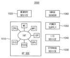
도 16을 참조하면, 전자 기기(2000)는 시스템 온 칩(1010), 메모리 장치(1020), 저장 장치(1030), 입출력 장치(1040), 파워 서플라이(1050) 및 이미지 센서(1060)를 포함할 수 있다. 한편, 도 16에는 도시되지 않았지만, 전자 기기(2000)는 비디오 카드, 사운드 카드, 메모리 카드, USB 장치 등과 통신하거나, 또는 다른 전자 기기들과 통신할 수 있는 포트(port)들을 더 포함할 수 있다.Referring to FIG. 16, the electronic device (2000) may include a system on chip (1010), a memory device (1020), a storage device (1030), an input/output device (1040), a power supply (1050), and an image sensor (1060). Meanwhile, although not shown in FIG. 16, the electronic device (2000) may further include ports that may communicate with a video card, a sound card, a memory card, a USB device, or the like, or communicate with other electronic devices.
시스템 온 칩(1010)은 애플리케이션 프로세서 시스템 온 칩(AP SOC)으로서 상호접속 장치(INT)와 이에 연결된 복수의 지능 소자들(또는 기능 블록들)을 포함할 수 있다. 예를 들어, 상기 지능 소자들은 메모리 콘트롤러(memory controller)(MC), 중앙 처리부(central processing unit), 디스플레이 콘트롤러(display controller)(DIS), 파일 시스템 블록(file system block)(FSYS), 그래픽 처리부(graphic processing unit)(GPU), 이미지 신호 프로세서(image signal processor)(ISP), 멀티 포맷 코덱 블록(multi-format codec block)(MFC) 등을 포함할 수 있다. 메모리 콘트롤러(MC)는 전술한 슬레이브 지능 소자들 중 하나에 해당하고 다른 지능 소자들 중 복수의 지능 소자들은 메모리 콘트롤러(MC)를 공통 자원으로 이용하는 마스터 지능 소자들에 해당한다. 이러한 마스터 지능 소자들 중 적어도 하나는 도 1 내지 도 15를 참조하여 설명한 바와 같이 본 발명의 실시예들에 따른 제어 방법을 수행하도록 구현될 수 있다.The system on chip (1010) may include an interconnect device (INT) and a plurality of intelligent elements (or functional blocks) connected thereto as an application processor system on chip (AP SOC). For example, the intelligent elements may include a memory controller (MC), a central processing unit (CPU), a display controller (DIS), a file system block (FSYS), a graphic processing unit (GPU), an image signal processor (ISP), a multi-format codec block (MFC), etc. The memory controller (MC) corresponds to one of the aforementioned slave intelligent elements, and a plurality of intelligent elements among the other intelligent elements correspond to master intelligent elements that use the memory controller (MC) as a common resource. At least one of these master intelligent elements may be implemented to perform a control method according to embodiments of the present invention as described with reference to FIGS. 1 to 15.
시스템 온 칩(1010)은 어드레스 버스(address bus), 제어 버스(control bus) 및 데이터 버스(data bus)를 통하여 메모리 장치(1020), 저장 장치(1030), 입출력 장치(1040) 및 이미지 센서(2060)와 통신을 수행할 수 있다. 실시예에 따라, 시스템 온 칩(1010)은 주변 구성요소 상호연결(Peripheral Component Interconnect; PCI) 버스와 같은 확장 버스에도 연결될 수 있다.The system on chip (1010) may communicate with a memory device (1020), a storage device (1030), an input/output device (1040), and an image sensor (2060) through an address bus, a control bus, and a data bus. According to an embodiment, the system on chip (1010) may also be connected to an expansion bus, such as a Peripheral Component Interconnect (PCI) bus.
메모리 장치(1020)는 전자 기기(2000)의 동작에 필요한 데이터 및 프로그램 코드를 저장할 수 있다. 예를 들어, 메모리 장치(1020)는 디램(DRAM), 모바일 디램, 에스램(SRAM), 피램(PRAM), 에프램(FRAM), 알램(RRAM) 및/또는 엠램(MRAM)으로 구현될 수 있다. 저장 장치(1030)는 솔리드 스테이트 드라이브(solid state drive), 하드 디스크 드라이브(hard disk drive), 씨디롬(CD-ROM) 등을 포함할 수 있다. 입출력 장치(1040)는 키보드, 키패드, 마우스 등과 같은 입력 수단 및 프린터, 디스플레이 등과 같은 출력 수단을 포함할 수 있다. 파워 서플라이(1050)는 전자 기기(2000)의 동작에 필요한 동작 전압을 공급할 수 있다.The memory device (1020) can store data and program codes required for the operation of the electronic device (2000). For example, the memory device (1020) can be implemented as DRAM, mobile DRAM, SRAM, PRAM, FRAM, RRAM, and/or MRAM. The storage device (1030) can include a solid state drive, a hard disk drive, a CD-ROM, and the like. The input/output device (1040) can include input means such as a keyboard, a keypad, a mouse, and the like, and output means such as a printer, a display, and the like. The power supply (1050) can supply an operating voltage required for the operation of the electronic device (2000).
이미지 센서(1060)는 상기 버스들 또는 다른 통신 링크를 통해서 시스템 온 칩(1010)과 연결되어 통신을 수행할 수 있다. 이미지 센서(1060)는 시스템 온 칩(1010)과 함께 하나의 칩에 집적될 수도 있고, 서로 다른 칩에 각각 집적될 수도 있다.The image sensor (1060) may be connected to the system on chip (1010) through the above buses or other communication links to perform communication. The image sensor (1060) may be integrated into one chip with the system on chip (1010) or may be integrated into different chips.
도 16에 도시된 전자 기기(2000)의 구성 요소들의 적어도 일부는 다양한 형태들의 패키지로 구현될 수 있다. 예를 들어, 적어도 일부의 구성들은 PoP(Package on Package), Ball grid arrays(BGAs), Chip scale packages(CSPs), Plastic Leaded Chip Carrier(PLCC), Plastic Dual In-Line Package(PDIP), Die in Waffle Pack, Die in Wafer Form, Chip On Board(COB), Ceramic Dual In-Line Package(CERDIP), Plastic Metric Quad Flat Pack(MQFP), Thin Quad Flatpack(TQFP), Small Outline(SOIC), Shrink Small Outline Package(SSOP), Thin Small Outline(TSOP), Thin Quad Flatpack(TQFP), System In Package(SIP), Multi Chip Package(MCP), Wafer-level Fabricated Package(WFP), Wafer-Level Processed Stack Package(WSP) 등과 같은 패키지들을 이용하여 실장될 수 있다.At least some of the components of the electronic device (2000) illustrated in FIG. 16 may be implemented as packages of various forms. For example, at least some of the components may be mounted using packages such as Package on Package (PoP), Ball grid arrays (BGAs), Chip scale packages (CSPs), Plastic Leaded Chip Carrier (PLCC), Plastic Dual In-Line Package (PDIP), Die in Waffle Pack, Die in Wafer Form, Chip On Board (COB), Ceramic Dual In-Line Package (CERDIP), Plastic Metric Quad Flat Pack (MQFP), Thin Quad Flatpack (TQFP), Small Outline (SOIC), Shrink Small Outline Package (SSOP), Thin Small Outline (TSOP), Thin Quad Flatpack (TQFP), System In Package (SIP), Multi Chip Package (MCP), Wafer-level Fabricated Package (WFP), Wafer-Level Processed Stack Package (WSP), etc.
한편, 전자 기기(2000)는 적어도 하나의 시스템 온 칩을 포함하는 모든 장치 및 시스템으로 해석되어야 할 것이다.Meanwhile, electronic devices (2000) should be interpreted as all devices and systems including at least one system on chip.
본 발명의 실시예들은 소모 전력의 감소가 요구되는 마스터 지능 소자 및 이를 포함하는 시스템에 유용하게 이용될 수 있다.Embodiments of the present invention can be usefully utilized in master intelligence devices and systems including the same where reduction in power consumption is required.
특히 본 발명의 실시예들은 컴퓨터(computer), 노트북(laptop), 핸드폰(cellular phone), 스마트폰(smart phone), MP3 플레이어, 피디에이(Personal Digital Assistants; PDA), 피엠피(Portable Multimedia Player; PMP), 디지털 TV, 디지털 카메라, 포터블 게임 콘솔(portable game console), 네비게이션(navigation) 기기, 웨어러블(wearable) 기기, IoT(internet of things;) 기기, IoE(internet of everything:) 기기, e-북(e-book), VR(virtual reality) 기기, AR(augmented reality) 기기 등과 같은 전자 기기에 더욱 유용하게 적용될 수 있다.In particular, embodiments of the present invention can be more usefully applied to electronic devices such as computers, laptops, cellular phones, smart phones, MP3 players, Personal Digital Assistants (PDAs), Portable Multimedia Players (PMPs), digital TVs, digital cameras, portable game consoles, navigation devices, wearable devices, Internet of Things (IoT) devices, Internet of Everything (IoE) devices, e-books, virtual reality (VR) devices, augmented reality (AR) devices, and the like.
상기에서는 본 발명이 바람직한 실시예를 참조하여 설명하였지만, 해당 기술분야의 숙련된 당업자는 하기의 특허청구범위에 기재된 본 발명의 사상 및 영역으로부터 벗어나지 않는 범위 내에서 본 발명을 다양하게 수정 및 변경시킬 수 있음을 이해할 것이다.Although the present invention has been described above with reference to preferred embodiments thereof, it will be understood by those skilled in the art that various modifications and changes may be made to the present invention without departing from the spirit and scope of the present invention as set forth in the claims below.
Claims (10)
Translated fromKorean상기 측정 서비스 수준에 기초하여 상기 마스터 지능 소자에 포함되는 리퀘스트 제어 회로의 전력 레벨을 제어하는 단계를 포함하고,
상기 리퀘스트 제어 회로의 전력 레벨을 제어하는 단계는,
상기 측정 서비스 수준이 증가할수록 상기 마스터 지능 소자가 발행할 수 있는 아웃스탠딩 리퀘스트들의 최대 개수를 감소하는 단계를 포함하고,
상기 리퀘스트 제어 회로는, 리퀘스트들을 각각 저장하기 위한 복수의 리퀘스트 저장 유닛들을 포함하고,
상기 복수의 리퀘스트 저장 유닛들 중 인에이블되는 리퀘스트 저장 유닛들의 개수는 상기 마스터 지능 소자가 발행할 수 있는 아웃스탠딩 리퀘스트들의 최대 개수에 해당하는 마스터 지능 소자의 제어 방법.A step of providing a measured service level by measuring in real time the service level of the requests of a master intelligent element which is connected to at least one slave intelligent element through an interconnection device and generates requests for requesting services from the slave intelligent element; and
A step of controlling the power level of the request control circuit included in the master intelligent element based on the above measurement service level,
The step of controlling the power level of the above request control circuit is:
Including a step of reducing the maximum number of outstanding requests that the master intelligent element can issue as the above measurement service level increases;
The above request control circuit includes a plurality of request storage units for storing requests, respectively.
A method for controlling a master intelligent element, wherein the number of enabled request storage units among the plurality of request storage units corresponds to the maximum number of outstanding requests that the master intelligent element can issue.
상기 리퀘스트 제어 회로의 전력 레벨을 제어하는 단계는,
상기 인에이블되는 리퀘스트 저장 유닛들의 개수를 변경하는 단계를 포함하는 것을 특징으로 하는 마스터 지능 소자의 제어 방법.In the first paragraph,
The step of controlling the power level of the above request control circuit is:
A method for controlling a master intelligent element, characterized by comprising a step of changing the number of enabled request storage units.
상기 인에이블되는 리퀘스트 저장 유닛들에는 동작 클록 신호 및 전원 전압을 공급하고 상기 복수의 리퀘스트 저장 유닛들 중에서 디스에이블되는 리퀘스트 저장 유닛들에 공급되는 상기 동작 클록 신호 및 상기 전원 전압을 차단하는 것을 특징으로 하는 마스터 지능 소자의 제어 방법.In the third paragraph,
A control method of a master intelligent element, characterized in that the enabled request storage units are supplied with an operation clock signal and a power supply voltage and the operation clock signal and the power supply voltage are blocked from being supplied to the disabled request storage units among the plurality of request storage units.
상기 인에이블되는 리퀘스트 저장 유닛들의 개수를 변경하는 단계는,
상기 측정 서비스 수준이 제1 기준 값보다 높게 증가하는 경우 상기 인에이블되는 리퀘스트 저장 유닛들의 개수를 N+1개에서 N개로 감소하는 단계; 및
상기 측정 서비스 수준이 상기 제1 기준 값보다 작은 제2 기준 값보다 낮게 감소하는 경우 상기 인에이블되는 리퀘스트 저장 유닛들의 개수를 N개에서 N+1개로 증가하는 단계를 포함하는 것을 특징으로 하는 마스터 지능 소자의 제어 방법.In the third paragraph,
The step of changing the number of enabled request storage units is:
A step of reducing the number of enabled request storage units from N+1 to N when the above measurement service level increases above the first reference value; and
A control method of a master intelligent element, characterized in that it comprises a step of increasing the number of enabled request storage units from N to N+1 when the measured service level decreases to a second reference value lower than the first reference value.
상기 리퀘스트 제어 회로의 전력 레벨을 제어하는 단계는,
상기 측정 서비스 수준이 증가할수록 상기 복수의 리퀘스트 저장 유닛들 중에서 동작 클록 신호 및 전원 전압을 공급받는 리퀘스트 저장 유닛들의 개수를 감소하는 단계를 포함하는 것을 특징으로 하는 마스터 지능 소자의 제어 방법.In the first paragraph,
The step of controlling the power level of the above request control circuit is:
A control method of a master intelligent element, characterized in that it includes a step of reducing the number of request storage units supplied with the operation clock signal and the power voltage among the plurality of request storage units as the above measurement service level increases.
상기 측정 서비스 수준을 제공하는 단계는,
상기 마스터 지능 소자에게 단위 시간 동안 전송되거나 서비스되는 데이터의 양에 상응하는 상기 마스터 지능 소자의 대역폭 및 상기 마스터 지능 소자가 상기 슬레이브 지능 소자에 대하여 서비스를 요청한 시점부터 상기 요청한 서비스가 완료되는 시점까지의 시간에 상응하는 상기 마스터 지능 소자의 레이턴시 중에서 적어도 하나를 측정하여 상기 측정 서비스 수준으로서 제공하는 단계를 포함하는 것을 특징으로 하는 마스터 지능 소자의 제어 방법.In the first paragraph,
The steps for providing the above measurement service level are:
A method for controlling a master intelligent element, characterized by comprising the step of measuring at least one of a bandwidth of the master intelligent element corresponding to the amount of data transmitted or serviced per unit time to the master intelligent element and a latency of the master intelligent element corresponding to the time from the time the master intelligent element requests a service to the slave intelligent element to the time the requested service is completed, and providing the measured service level.
마스터 지능 소자의 상기 리퀘스트들에 대한 서비스 수준을 실시간으로 측정하여 측정 서비스 수준을 제공하는 서비스 수준 모니터; 및
상기 측정 서비스 수준에 기초하여 전력 레벨을 제어하는 리퀘스트 제어 회로를 포함하고,
상기 측정 서비스 수준이 증가할수록 상기 마스터 지능 소자가 발행할 수 있는 아웃스탠딩 리퀘스트들의 최대 개수를 감소하고,
상기 리퀘스트 제어 회로는, 리퀘스트들을 각각 저장하기 위한 복수의 리퀘스트 저장 유닛들을 포함하고,
상기 복수의 리퀘스트 저장 유닛들 중 인에이블되는 리퀘스트 저장 유닛들의 개수는 상기 마스터 지능 소자가 발행할 수 있는 아웃스탠딩 리퀘스트들의 최대 개수에 해당하는 마스터 지능 소자.A master intelligent element connected to at least one slave intelligent element through an interconnection device and generating requests for requesting services from said slave intelligent element,
A service level monitor that measures the service level of the above requests of the master intelligent element in real time and provides a measured service level; and
A request control circuit for controlling a power level based on the above measurement service level is included.
As the above measurement service level increases, the maximum number of outstanding requests that the master intelligent element can issue decreases,
The above request control circuit includes a plurality of request storage units for storing requests, respectively.
A master intelligence element wherein the number of enabled request storage units among the above plurality of request storage units corresponds to the maximum number of outstanding requests that the master intelligence element can issue.
상기 리퀘스트 제어 회로는,
상기 복수의 리퀘스트 저장 유닛들을 포함하는 리퀘스트 큐;
상기 측정 서비스 수준에 기초하여 상기 마스터 지능 소자가 발행할 수 있는 아웃스탠딩 리퀘스트들의 최대 개수를 결정하는 리소스 콘트롤러; 및
상기 복수의 리퀘스트 저장 유닛들에 공급되는 동작 클록 신호 및 전원 전압을 각각 게이팅하는 복수의 스위치들을 포함하는 게이트 회로를 포함하는 것을 특징으로 하는 마스터 지능 소자.In Article 8,
The above request control circuit,
A request queue including a plurality of request storage units;
A resource controller that determines the maximum number of outstanding requests that the master intelligent element can issue based on the measured service level; and
A master intelligence element characterized by comprising a gate circuit including a plurality of switches each of which gates an operating clock signal and a power supply voltage supplied to the plurality of request storage units.
상기 리소스 콘트롤러는,
상기 복수의 스위치들의 스위칭 동작을 각각 제어하기 위한 복수의 스위치 제어 신호들을 발생하고,
상기 측정 서비스 수준에 기초하여 상기 복수의 스위치 제어 신호들 중에서 활성화되는 스위치 제어 신호들의 개수를 변경하는 것을 특징으로 하는 마스터 지능 소자.
In Article 9,
The above resource controller,
Generating a plurality of switch control signals for respectively controlling the switching operations of the plurality of switches,
A master intelligence element characterized in that the number of switch control signals activated among the plurality of switch control signals is changed based on the above measurement service level.
Priority Applications (3)
| Application Number | Priority Date | Filing Date | Title |
|---|---|---|---|
| KR1020190090170AKR102818463B1 (en) | 2019-07-25 | 2019-07-25 | Master device and method of controlling the same |
| US16/816,992US11418361B2 (en) | 2019-07-25 | 2020-03-12 | Master device, system and method of controlling the same |
| CN202010648880.9ACN112286335B (en) | 2019-07-25 | 2020-07-07 | Master device, and system and method for controlling the same |
Applications Claiming Priority (1)
| Application Number | Priority Date | Filing Date | Title |
|---|---|---|---|
| KR1020190090170AKR102818463B1 (en) | 2019-07-25 | 2019-07-25 | Master device and method of controlling the same |
Publications (2)
| Publication Number | Publication Date |
|---|---|
| KR20210012439A KR20210012439A (en) | 2021-02-03 |
| KR102818463B1true KR102818463B1 (en) | 2025-06-10 |
Family
ID=74189154
Family Applications (1)
| Application Number | Title | Priority Date | Filing Date |
|---|---|---|---|
| KR1020190090170AActiveKR102818463B1 (en) | 2019-07-25 | 2019-07-25 | Master device and method of controlling the same |
Country Status (3)
| Country | Link |
|---|---|
| US (1) | US11418361B2 (en) |
| KR (1) | KR102818463B1 (en) |
| CN (1) | CN112286335B (en) |
Families Citing this family (1)
| Publication number | Priority date | Publication date | Assignee | Title |
|---|---|---|---|---|
| AU2022396273A1 (en)* | 2021-11-23 | 2024-05-30 | Strong Force TX Portfolio 2018, LLC | Transaction platforms where systems include sets of other systems |
Family Cites Families (87)
| Publication number | Priority date | Publication date | Assignee | Title |
|---|---|---|---|---|
| JP2000035928A (en)* | 1998-07-16 | 2000-02-02 | Yazaki Corp | Network monitoring system and method |
| US7366822B2 (en)* | 2001-11-26 | 2008-04-29 | Samsung Electronics Co., Ltd. | Semiconductor memory device capable of reading and writing data at the same time |
| US6892281B2 (en)* | 2002-10-03 | 2005-05-10 | Intel Corporation | Apparatus, method, and system for reducing latency of memory devices |
| US7564871B2 (en)* | 2002-10-25 | 2009-07-21 | At&T Corp. | Network routing method and system utilizing label-switching traffic engineering queues |
| US7395380B2 (en)* | 2003-03-20 | 2008-07-01 | International Business Machines Corporation | Selective snooping by snoop masters to locate updated data |
| US6956401B1 (en)* | 2003-11-10 | 2005-10-18 | Altera Corporation | Differential input buffers with elevated power supplies |
| DE602004021771D1 (en)* | 2004-04-30 | 2009-08-13 | St Microelectronics Res & Dev | Resource Management |
| EP1820309B1 (en)* | 2004-12-03 | 2008-08-27 | Koninklijke Philips Electronics N.V. | Streaming memory controller |
| US7738483B2 (en)* | 2005-09-08 | 2010-06-15 | Kabushiki Kaisha Toshiba | Systems and methods for managing communication between master and slave devices |
| US8201172B1 (en)* | 2005-12-14 | 2012-06-12 | Nvidia Corporation | Multi-threaded FIFO memory with speculative read and write capability |
| US8155712B2 (en)* | 2006-03-23 | 2012-04-10 | Sibeam, Inc. | Low power very high-data rate device |
| KR101405969B1 (en)* | 2007-06-28 | 2014-06-13 | 엘지전자 주식회사 | Digital broadcasting system and data processing method |
| JP2009049642A (en)* | 2007-08-17 | 2009-03-05 | Omron Corp | Transmission system |
| US7925853B2 (en)* | 2008-01-04 | 2011-04-12 | International Business Machines Corporation | Method and apparatus for controlling memory array gating when a processor executes a low confidence branch instruction in an information handling system |
| US7991921B2 (en)* | 2008-03-11 | 2011-08-02 | Freescale Semiconductor, Inc. | System and method for reducing power consumption of memory in an I/O controller |
| US8843691B2 (en)* | 2008-06-25 | 2014-09-23 | Stec, Inc. | Prioritized erasure of data blocks in a flash storage device |
| US8255562B2 (en)* | 2008-06-30 | 2012-08-28 | International Business Machines Corporation | Adaptive data throttling for storage controllers |
| US8127153B2 (en)* | 2008-07-29 | 2012-02-28 | Oracle America, Inc. | Memory power profiling |
| US9014640B2 (en)* | 2008-10-31 | 2015-04-21 | Qualcomm Incorporated | Wake-up trigger for implementation of target actions |
| DE102008059204B9 (en)* | 2008-11-27 | 2011-05-05 | Infineon Technologies Ag | Method for searching for a slave node in a communication network, master node and slave node for a communication network |
| US8572418B2 (en)* | 2009-03-12 | 2013-10-29 | Qualcomm Incorporated | Moving clock gating cell closer to clock source based on enable signal propagation time to clocked storage element |
| TW201037711A (en)* | 2009-04-13 | 2010-10-16 | Jmicron Technology Corp | Data access method used in multi-channel flash memory system and data access apparatus thereof |
| US8103894B2 (en)* | 2009-04-24 | 2012-01-24 | International Business Machines Corporation | Power conservation in vertically-striped NUCA caches |
| JP5467558B2 (en)* | 2009-09-09 | 2014-04-09 | アラクサラネットワークス株式会社 | Network relay device and memory control method |
| US9246826B2 (en)* | 2009-11-11 | 2016-01-26 | Synopsys, Inc. | Integrated circuit arrangement for buffering service requests |
| US20110173352A1 (en)* | 2010-01-13 | 2011-07-14 | Mellanox Technologies Ltd | Power Reduction on Idle Communication Lanes |
| KR20110114957A (en)* | 2010-04-14 | 2011-10-20 | 삼성전기주식회사 | Data transmission apparatus and method, network data transmission system and method using same |
| US9842068B2 (en)* | 2010-04-14 | 2017-12-12 | Qualcomm Incorporated | Methods of bus arbitration for low power memory access |
| KR101835615B1 (en)* | 2010-05-07 | 2018-03-09 | 삼성전자주식회사 | SYSTEM ON CHIP, DEVICES HAVING THE SAME, AND METHOD FOR POWER CONTROL OF THE SoC |
| CA2794728A1 (en)* | 2010-06-16 | 2011-12-22 | Ndi Technologies, Inc. | Usb video interface for alpr cameras and associated method |
| JP5434812B2 (en)* | 2010-06-21 | 2014-03-05 | 富士通セミコンダクター株式会社 | Data processing system |
| US8904115B2 (en)* | 2010-09-28 | 2014-12-02 | Texas Instruments Incorporated | Cache with multiple access pipelines |
| WO2012054019A1 (en)* | 2010-10-19 | 2012-04-26 | Hewlett-Packard Development Company, L.P. | Systems and methods for predictive control of power efficiency |
| JP5625737B2 (en)* | 2010-10-22 | 2014-11-19 | 富士通株式会社 | Transfer device, transfer method, and transfer program |
| US8972689B1 (en)* | 2011-02-02 | 2015-03-03 | Violin Memory, Inc. | Apparatus, method and system for using real-time performance feedback for modeling and improving access to solid state media |
| JP5738618B2 (en)* | 2011-02-08 | 2015-06-24 | オリンパス株式会社 | Data processing device |
| JP5706297B2 (en)* | 2011-02-18 | 2015-04-22 | アラクサラネットワークス株式会社 | Packet transfer apparatus and power supply control method for QoS control circuit |
| KR101842245B1 (en) | 2011-07-25 | 2018-03-26 | 삼성전자주식회사 | Bus system in SoC and method of gating root clocks therefor |
| US9058167B2 (en)* | 2011-09-06 | 2015-06-16 | Cisco Technology, Inc. | Power conservation in a distributed digital video recorder/content delivery network system |
| JP2013106166A (en) | 2011-11-14 | 2013-05-30 | Sony Corp | Clock gating circuit and bus system |
| US9158461B1 (en)* | 2012-01-18 | 2015-10-13 | Western Digital Technologies, Inc. | Measuring performance of data storage systems |
| US9264368B2 (en)* | 2012-01-27 | 2016-02-16 | Marvell World Trade Ltd. | Chip-to-chip communications |
| US9930094B2 (en)* | 2012-03-27 | 2018-03-27 | Industry-Academic Cooperation of Yonsei University | Content complex providing server for a group of terminals |
| KR101949382B1 (en)* | 2012-04-04 | 2019-02-18 | 삼성전자주식회사 | System on chip of enhancing quality of service and method of controlling a system on chip |
| KR20140013401A (en)* | 2012-07-23 | 2014-02-05 | 삼성전자주식회사 | Memory device, memory system and method of controlling a read voltage of the memory device |
| JP5975446B2 (en)* | 2012-08-13 | 2016-08-23 | パナソニックIpマネジメント株式会社 | Access control device, relay device, access control method, computer program |
| US20140052906A1 (en)* | 2012-08-17 | 2014-02-20 | Rambus Inc. | Memory controller responsive to latency-sensitive applications and mixed-granularity access requests |
| EP2701411B1 (en)* | 2012-08-21 | 2018-02-28 | BlackBerry Limited | Smart proximity priority pairing |
| KR101932920B1 (en)* | 2012-09-14 | 2019-03-18 | 삼성전자 주식회사 | Host for controlling non-volatile memory crad, system including the same and operating method there-of |
| KR20140036622A (en)* | 2012-09-17 | 2014-03-26 | 한국전자통신연구원 | Apparatus and method for lane fault recovery of multi-lane based ethernet |
| WO2014065389A1 (en)* | 2012-10-25 | 2014-05-01 | Semiconductor Energy Laboratory Co., Ltd. | Central control system |
| WO2014096970A2 (en)* | 2012-12-20 | 2014-06-26 | Marvell World Trade Ltd. | Memory sharing in a network device |
| KR102021795B1 (en)* | 2013-01-24 | 2019-09-17 | 삼성전자주식회사 | Adaptive service controller, system on chip and method of controlling the same |
| US9684633B2 (en)* | 2013-01-24 | 2017-06-20 | Samsung Electronics Co., Ltd. | Adaptive service controller, system on chip and method of controlling the same |
| JP6229985B2 (en)* | 2013-03-12 | 2017-11-15 | パナソニックIpマネジメント株式会社 | Bus system and computer program |
| DE112014001621T5 (en)* | 2013-03-25 | 2015-12-24 | Mitsubishi Electric Corporation | Bus master, bus system and bus control method |
| US9442668B1 (en) | 2013-08-29 | 2016-09-13 | Western Digital Technologies, Inc. | Adaptive power management control with performance feedback |
| US9395795B2 (en) | 2013-09-20 | 2016-07-19 | Apple Inc. | System power management using communication bus protocols |
| GB2518884A (en)* | 2013-10-04 | 2015-04-08 | Ibm | Network attached storage system and corresponding method for request handling in a network attached storage system |
| EP3120216B1 (en)* | 2014-03-20 | 2020-11-04 | Intel Corporation | A method, apparatus, and system for controlling power consumption of unused hardware of a link interface |
| CN105101248B (en)* | 2014-04-28 | 2020-03-13 | 索尼公司 | Apparatus and method for controlling change of operating state of cell |
| US20150363116A1 (en) | 2014-06-12 | 2015-12-17 | Advanced Micro Devices, Inc. | Memory controller power management based on latency |
| US9766681B2 (en)* | 2014-06-17 | 2017-09-19 | Empire Technology Development Llc | Operations related to a retransmission buffer |
| US9647545B2 (en)* | 2014-10-20 | 2017-05-09 | Qualcomm Incorporated | Reduced sleep current in power converters |
| US9887918B1 (en)* | 2014-11-02 | 2018-02-06 | Netronome Systems, Inc. | Intelligent packet data register file that stalls picoengine and retrieves data from a larger buffer |
| US9817602B2 (en)* | 2014-11-13 | 2017-11-14 | Violin Systems Llc | Non-volatile buffering for deduplication |
| CN105677605B (en)* | 2014-11-20 | 2019-04-30 | 深圳市中兴微电子技术有限公司 | An efficient configurable on-chip interconnection system and its realization method and device |
| US9634901B2 (en)* | 2015-01-29 | 2017-04-25 | Knuedge Incorporated | Topology discovery in a computing system |
| US9760281B2 (en)* | 2015-03-27 | 2017-09-12 | Intel Corporation | Sequential write stream management |
| CN105024892A (en)* | 2015-06-09 | 2015-11-04 | 上海冉能自动化科技有限公司 | A method and system realizing wireless communication between an instrument and a host computer |
| US9860841B2 (en) | 2015-08-20 | 2018-01-02 | Apple Inc. | Communications fabric with split paths for control and data packets |
| US10218780B2 (en)* | 2016-04-20 | 2019-02-26 | Wyse Technology L.L.C. | Cloud based peer assisted updates in a device management environment |
| KR102743928B1 (en)* | 2016-08-04 | 2024-12-18 | 삼성전자주식회사 | Storage device, test system for testing the same, and method thereof |
| US10394724B2 (en) | 2016-08-22 | 2019-08-27 | Qualcomm Incorporated | Low power data transfer for memory subsystem using data pattern checker to determine when to suppress transfers based on specific patterns |
| KR102595903B1 (en)* | 2016-08-26 | 2023-10-30 | 삼성전자주식회사 | Modem Chip, Application Processor including the same and Operating Method of Modem Chip |
| US20190065243A1 (en)* | 2016-09-19 | 2019-02-28 | Advanced Micro Devices, Inc. | Dynamic memory power capping with criticality awareness |
| US11243600B2 (en)* | 2017-07-03 | 2022-02-08 | Industry-University Cooperation Foundation Hanyang University | HMC control device and method of CPU side and HMC side for low power mode, and power management method of HMC control device |
| US10579568B2 (en)* | 2017-07-03 | 2020-03-03 | Intel Corporation | Networked storage system with access to any attached storage device |
| BR102017019865A2 (en)* | 2017-09-15 | 2019-04-16 | Velsis Sistemas E Tecnologia Viaria S/A | PREDICTIVE, INTEGRATED AND INTELLIGENT SYSTEM FOR TRAFFIC TRAFFIC TIME CONTROL |
| US10861504B2 (en) | 2017-10-05 | 2020-12-08 | Advanced Micro Devices, Inc. | Dynamic control of multi-region fabric |
| US10522201B2 (en)* | 2018-05-31 | 2019-12-31 | Qualcomm Incorporated | Methods and systems for serial memory device control |
| CN110729006B (en)* | 2018-07-16 | 2022-07-05 | 超威半导体(上海)有限公司 | Refresh Schemes in Memory Controllers |
| CN108973979B (en)* | 2018-07-18 | 2021-09-28 | 乾碳国际公司 | Hybrid vehicle predictive power control system scheme |
| WO2020026036A1 (en)* | 2018-07-31 | 2020-02-06 | Marvell World Trade Ltd. | Metadata generation at the storage edge |
| US20200042500A1 (en)* | 2018-08-02 | 2020-02-06 | Alibaba Group Holding Limited | Collaborative compression in a distributed storage system |
| CN110943783B (en)* | 2018-09-25 | 2022-08-19 | 中兴通讯股份有限公司 | Distance measurement method of optical network, OLT, ONU and optical network system |
| US11036279B2 (en)* | 2019-04-29 | 2021-06-15 | Arm Limited | Apparatus and method for managing a cache |
- 2019
- 2019-07-25KRKR1020190090170Apatent/KR102818463B1/enactiveActive
- 2020
- 2020-03-12USUS16/816,992patent/US11418361B2/enactiveActive
- 2020-07-07CNCN202010648880.9Apatent/CN112286335B/enactiveActive
Also Published As
| Publication number | Publication date |
|---|---|
| KR20210012439A (en) | 2021-02-03 |
| CN112286335A (en) | 2021-01-29 |
| US11418361B2 (en) | 2022-08-16 |
| CN112286335B (en) | 2024-05-14 |
| US20210028956A1 (en) | 2021-01-28 |
Similar Documents
| Publication | Publication Date | Title |
|---|---|---|
| KR101949382B1 (en) | System on chip of enhancing quality of service and method of controlling a system on chip | |
| US9684633B2 (en) | Adaptive service controller, system on chip and method of controlling the same | |
| US11748284B2 (en) | Systems and methods for arbitrating traffic in a bus | |
| US11886365B2 (en) | DMA control circuit with quality of service indications | |
| US10423558B1 (en) | Systems and methods for controlling data on a bus using latency | |
| US11809906B2 (en) | Systems and methods to control bandwidth through shared transaction limits | |
| US10649922B2 (en) | Systems and methods for scheduling different types of memory requests with varying data sizes | |
| CN113535634B (en) | Electronic device and method for bandwidth allocation | |
| US20180095910A1 (en) | Preserving deterministic early valid across a clock domain crossing | |
| US20100070667A1 (en) | Arbitration Based Allocation of a Shared Resource with Reduced Latencies | |
| KR102818463B1 (en) | Master device and method of controlling the same | |
| US8527684B2 (en) | Closed loop dynamic interconnect bus allocation method and architecture for a multi layer SoC | |
| US11886367B2 (en) | Arbitration allocating requests during backpressure | |
| US10963172B2 (en) | Systems and methods for providing a back pressure free interconnect | |
| JP7616321B2 (en) | Task scheduler device and program | |
| US10664396B2 (en) | Systems, methods and apparatus for fabric delta merge operations to enhance NVMeoF stream writes | |
| US11675718B2 (en) | Enhanced low-priority arbitration | |
| KR102021795B1 (en) | Adaptive service controller, system on chip and method of controlling the same | |
| US10877888B2 (en) | Systems and methods for providing distributed global ordering | |
| WO2022143019A1 (en) | Heterogeneous computing system and related device | |
| US10073723B2 (en) | Dynamic range-based messaging | |
| US11138111B2 (en) | Parallel coherence and memory cache processing pipelines | |
| US20140143462A1 (en) | Register slicing circuit and system on chip including the same | |
| KR20180074197A (en) | Bus traffic control apparatus and bus system having the same | |
| CN116627316A (en) | Memory system for trimming data, operation method thereof, and host system for controlling same |
Legal Events
| Date | Code | Title | Description |
|---|---|---|---|
| PA0109 | Patent application | Patent event code:PA01091R01D Comment text:Patent Application Patent event date:20190725 | |
| PG1501 | Laying open of application | ||
| PA0201 | Request for examination | Patent event code:PA02012R01D Patent event date:20220526 Comment text:Request for Examination of Application Patent event code:PA02011R01I Patent event date:20190725 Comment text:Patent Application | |
| E902 | Notification of reason for refusal | ||
| PE0902 | Notice of grounds for rejection | Comment text:Notification of reason for refusal Patent event date:20240424 Patent event code:PE09021S01D | |
| E601 | Decision to refuse application | ||
| PE0601 | Decision on rejection of patent | Patent event date:20241211 Comment text:Decision to Refuse Application Patent event code:PE06012S01D | |
| AMND | Amendment | ||
| PX0901 | Re-examination | Patent event code:PX09012R01I Patent event date:20250310 Comment text:Amendment to Specification, etc. | |
| PX0701 | Decision of registration after re-examination | Patent event date:20250401 Comment text:Decision to Grant Registration Patent event code:PX07013S01D | |
| X701 | Decision to grant (after re-examination) | ||
| GRNT | Written decision to grant | ||
| PR0701 | Registration of establishment | Comment text:Registration of Establishment Patent event date:20250604 Patent event code:PR07011E01D | |
| PR1002 | Payment of registration fee | Payment date:20250605 End annual number:3 Start annual number:1 | |
| PG1601 | Publication of registration |