KR102816013B1 - Memory device and opearting method thereof - Google Patents
Memory device and opearting method thereofDownload PDFInfo
- Publication number
- KR102816013B1 KR102816013B1KR1020200091955AKR20200091955AKR102816013B1KR 102816013 B1KR102816013 B1KR 102816013B1KR 1020200091955 AKR1020200091955 AKR 1020200091955AKR 20200091955 AKR20200091955 AKR 20200091955AKR 102816013 B1KR102816013 B1KR 102816013B1
- Authority
- KR
- South Korea
- Prior art keywords
- control
- control code
- memory
- command
- memory device
- Prior art date
- Legal status (The legal status is an assumption and is not a legal conclusion. Google has not performed a legal analysis and makes no representation as to the accuracy of the status listed.)
- Active
Links
Images


Classifications
- G—PHYSICS
- G06—COMPUTING OR CALCULATING; COUNTING
- G06F—ELECTRIC DIGITAL DATA PROCESSING
- G06F3/00—Input arrangements for transferring data to be processed into a form capable of being handled by the computer; Output arrangements for transferring data from processing unit to output unit, e.g. interface arrangements
- G06F3/06—Digital input from, or digital output to, record carriers, e.g. RAID, emulated record carriers or networked record carriers
- G06F3/0601—Interfaces specially adapted for storage systems
- G06F3/0628—Interfaces specially adapted for storage systems making use of a particular technique
- G06F3/0655—Vertical data movement, i.e. input-output transfer; data movement between one or more hosts and one or more storage devices
- G06F3/0659—Command handling arrangements, e.g. command buffers, queues, command scheduling
- G—PHYSICS
- G11—INFORMATION STORAGE
- G11C—STATIC STORES
- G11C16/00—Erasable programmable read-only memories
- G11C16/02—Erasable programmable read-only memories electrically programmable
- G11C16/06—Auxiliary circuits, e.g. for writing into memory
- G11C16/08—Address circuits; Decoders; Word-line control circuits
- G—PHYSICS
- G06—COMPUTING OR CALCULATING; COUNTING
- G06F—ELECTRIC DIGITAL DATA PROCESSING
- G06F12/00—Accessing, addressing or allocating within memory systems or architectures
- G06F12/02—Addressing or allocation; Relocation
- G06F12/06—Addressing a physical block of locations, e.g. base addressing, module addressing, memory dedication
- G06F12/0607—Interleaved addressing
- G—PHYSICS
- G06—COMPUTING OR CALCULATING; COUNTING
- G06F—ELECTRIC DIGITAL DATA PROCESSING
- G06F12/00—Accessing, addressing or allocating within memory systems or architectures
- G06F12/02—Addressing or allocation; Relocation
- G06F12/08—Addressing or allocation; Relocation in hierarchically structured memory systems, e.g. virtual memory systems
- G06F12/0802—Addressing of a memory level in which the access to the desired data or data block requires associative addressing means, e.g. caches
- G06F12/0877—Cache access modes
- G06F12/0882—Page mode
- G—PHYSICS
- G06—COMPUTING OR CALCULATING; COUNTING
- G06F—ELECTRIC DIGITAL DATA PROCESSING
- G06F13/00—Interconnection of, or transfer of information or other signals between, memories, input/output devices or central processing units
- G06F13/14—Handling requests for interconnection or transfer
- G06F13/16—Handling requests for interconnection or transfer for access to memory bus
- G06F13/1605—Handling requests for interconnection or transfer for access to memory bus based on arbitration
- G06F13/1642—Handling requests for interconnection or transfer for access to memory bus based on arbitration with request queuing
- G—PHYSICS
- G06—COMPUTING OR CALCULATING; COUNTING
- G06F—ELECTRIC DIGITAL DATA PROCESSING
- G06F13/00—Interconnection of, or transfer of information or other signals between, memories, input/output devices or central processing units
- G06F13/14—Handling requests for interconnection or transfer
- G06F13/16—Handling requests for interconnection or transfer for access to memory bus
- G06F13/1605—Handling requests for interconnection or transfer for access to memory bus based on arbitration
- G06F13/1647—Handling requests for interconnection or transfer for access to memory bus based on arbitration with interleaved bank access
- G—PHYSICS
- G06—COMPUTING OR CALCULATING; COUNTING
- G06F—ELECTRIC DIGITAL DATA PROCESSING
- G06F13/00—Interconnection of, or transfer of information or other signals between, memories, input/output devices or central processing units
- G06F13/14—Handling requests for interconnection or transfer
- G06F13/16—Handling requests for interconnection or transfer for access to memory bus
- G06F13/1668—Details of memory controller
- G06F13/1673—Details of memory controller using buffers
- G—PHYSICS
- G06—COMPUTING OR CALCULATING; COUNTING
- G06F—ELECTRIC DIGITAL DATA PROCESSING
- G06F13/00—Interconnection of, or transfer of information or other signals between, memories, input/output devices or central processing units
- G06F13/38—Information transfer, e.g. on bus
- G06F13/42—Bus transfer protocol, e.g. handshake; Synchronisation
- G06F13/4204—Bus transfer protocol, e.g. handshake; Synchronisation on a parallel bus
- G06F13/4221—Bus transfer protocol, e.g. handshake; Synchronisation on a parallel bus being an input/output bus, e.g. ISA bus, EISA bus, PCI bus, SCSI bus
- G—PHYSICS
- G06—COMPUTING OR CALCULATING; COUNTING
- G06F—ELECTRIC DIGITAL DATA PROCESSING
- G06F3/00—Input arrangements for transferring data to be processed into a form capable of being handled by the computer; Output arrangements for transferring data from processing unit to output unit, e.g. interface arrangements
- G06F3/06—Digital input from, or digital output to, record carriers, e.g. RAID, emulated record carriers or networked record carriers
- G06F3/0601—Interfaces specially adapted for storage systems
- G06F3/0602—Interfaces specially adapted for storage systems specifically adapted to achieve a particular effect
- G06F3/0604—Improving or facilitating administration, e.g. storage management
- G—PHYSICS
- G06—COMPUTING OR CALCULATING; COUNTING
- G06F—ELECTRIC DIGITAL DATA PROCESSING
- G06F3/00—Input arrangements for transferring data to be processed into a form capable of being handled by the computer; Output arrangements for transferring data from processing unit to output unit, e.g. interface arrangements
- G06F3/06—Digital input from, or digital output to, record carriers, e.g. RAID, emulated record carriers or networked record carriers
- G06F3/0601—Interfaces specially adapted for storage systems
- G06F3/0602—Interfaces specially adapted for storage systems specifically adapted to achieve a particular effect
- G06F3/061—Improving I/O performance
- G—PHYSICS
- G06—COMPUTING OR CALCULATING; COUNTING
- G06F—ELECTRIC DIGITAL DATA PROCESSING
- G06F3/00—Input arrangements for transferring data to be processed into a form capable of being handled by the computer; Output arrangements for transferring data from processing unit to output unit, e.g. interface arrangements
- G06F3/06—Digital input from, or digital output to, record carriers, e.g. RAID, emulated record carriers or networked record carriers
- G06F3/0601—Interfaces specially adapted for storage systems
- G06F3/0628—Interfaces specially adapted for storage systems making use of a particular technique
- G06F3/0638—Organizing or formatting or addressing of data
- G06F3/064—Management of blocks
- G—PHYSICS
- G06—COMPUTING OR CALCULATING; COUNTING
- G06F—ELECTRIC DIGITAL DATA PROCESSING
- G06F3/00—Input arrangements for transferring data to be processed into a form capable of being handled by the computer; Output arrangements for transferring data from processing unit to output unit, e.g. interface arrangements
- G06F3/06—Digital input from, or digital output to, record carriers, e.g. RAID, emulated record carriers or networked record carriers
- G06F3/0601—Interfaces specially adapted for storage systems
- G06F3/0628—Interfaces specially adapted for storage systems making use of a particular technique
- G06F3/0655—Vertical data movement, i.e. input-output transfer; data movement between one or more hosts and one or more storage devices
- G06F3/0656—Data buffering arrangements
- G—PHYSICS
- G06—COMPUTING OR CALCULATING; COUNTING
- G06F—ELECTRIC DIGITAL DATA PROCESSING
- G06F3/00—Input arrangements for transferring data to be processed into a form capable of being handled by the computer; Output arrangements for transferring data from processing unit to output unit, e.g. interface arrangements
- G06F3/06—Digital input from, or digital output to, record carriers, e.g. RAID, emulated record carriers or networked record carriers
- G06F3/0601—Interfaces specially adapted for storage systems
- G06F3/0668—Interfaces specially adapted for storage systems adopting a particular infrastructure
- G06F3/0671—In-line storage system
- G06F3/0673—Single storage device
- G06F3/0679—Non-volatile semiconductor memory device, e.g. flash memory, one time programmable memory [OTP]
- G—PHYSICS
- G11—INFORMATION STORAGE
- G11C—STATIC STORES
- G11C11/00—Digital stores characterised by the use of particular electric or magnetic storage elements; Storage elements therefor
- G11C11/56—Digital stores characterised by the use of particular electric or magnetic storage elements; Storage elements therefor using storage elements with more than two stable states represented by steps, e.g. of voltage, current, phase, frequency
- G11C11/5621—Digital stores characterised by the use of particular electric or magnetic storage elements; Storage elements therefor using storage elements with more than two stable states represented by steps, e.g. of voltage, current, phase, frequency using charge storage in a floating gate
- G11C11/5628—Programming or writing circuits; Data input circuits
- G—PHYSICS
- G11—INFORMATION STORAGE
- G11C—STATIC STORES
- G11C11/00—Digital stores characterised by the use of particular electric or magnetic storage elements; Storage elements therefor
- G11C11/56—Digital stores characterised by the use of particular electric or magnetic storage elements; Storage elements therefor using storage elements with more than two stable states represented by steps, e.g. of voltage, current, phase, frequency
- G11C11/5621—Digital stores characterised by the use of particular electric or magnetic storage elements; Storage elements therefor using storage elements with more than two stable states represented by steps, e.g. of voltage, current, phase, frequency using charge storage in a floating gate
- G11C11/5642—Sensing or reading circuits; Data output circuits
- G—PHYSICS
- G11—INFORMATION STORAGE
- G11C—STATIC STORES
- G11C11/00—Digital stores characterised by the use of particular electric or magnetic storage elements; Storage elements therefor
- G11C11/56—Digital stores characterised by the use of particular electric or magnetic storage elements; Storage elements therefor using storage elements with more than two stable states represented by steps, e.g. of voltage, current, phase, frequency
- G11C11/5671—Digital stores characterised by the use of particular electric or magnetic storage elements; Storage elements therefor using storage elements with more than two stable states represented by steps, e.g. of voltage, current, phase, frequency using charge trapping in an insulator
- G—PHYSICS
- G11—INFORMATION STORAGE
- G11C—STATIC STORES
- G11C16/00—Erasable programmable read-only memories
- G11C16/02—Erasable programmable read-only memories electrically programmable
- G11C16/04—Erasable programmable read-only memories electrically programmable using variable threshold transistors, e.g. FAMOS
- G11C16/0483—Erasable programmable read-only memories electrically programmable using variable threshold transistors, e.g. FAMOS comprising cells having several storage transistors connected in series
- G—PHYSICS
- G11—INFORMATION STORAGE
- G11C—STATIC STORES
- G11C16/00—Erasable programmable read-only memories
- G11C16/02—Erasable programmable read-only memories electrically programmable
- G11C16/06—Auxiliary circuits, e.g. for writing into memory
- G11C16/26—Sensing or reading circuits; Data output circuits
- G—PHYSICS
- G11—INFORMATION STORAGE
- G11C—STATIC STORES
- G11C5/00—Details of stores covered by group G11C11/00
- G11C5/14—Power supply arrangements, e.g. power down, chip selection or deselection, layout of wirings or power grids, or multiple supply levels
- G11C5/147—Voltage reference generators, voltage or current regulators; Internally lowered supply levels; Compensation for voltage drops
- G—PHYSICS
- G11—INFORMATION STORAGE
- G11C—STATIC STORES
- G11C7/00—Arrangements for writing information into, or reading information out from, a digital store
- G11C7/10—Input/output [I/O] data interface arrangements, e.g. I/O data control circuits, I/O data buffers
- G11C7/1015—Read-write modes for single port memories, i.e. having either a random port or a serial port
- G11C7/1036—Read-write modes for single port memories, i.e. having either a random port or a serial port using data shift registers
- G—PHYSICS
- G11—INFORMATION STORAGE
- G11C—STATIC STORES
- G11C7/00—Arrangements for writing information into, or reading information out from, a digital store
- G11C7/10—Input/output [I/O] data interface arrangements, e.g. I/O data control circuits, I/O data buffers
- G11C7/1015—Read-write modes for single port memories, i.e. having either a random port or a serial port
- G11C7/1042—Read-write modes for single port memories, i.e. having either a random port or a serial port using interleaving techniques, i.e. read-write of one part of the memory while preparing another part
- G—PHYSICS
- G11—INFORMATION STORAGE
- G11C—STATIC STORES
- G11C7/00—Arrangements for writing information into, or reading information out from, a digital store
- G11C7/18—Bit line organisation; Bit line lay-out
- G—PHYSICS
- G11—INFORMATION STORAGE
- G11C—STATIC STORES
- G11C8/00—Arrangements for selecting an address in a digital store
- G11C8/14—Word line organisation; Word line lay-out
- G—PHYSICS
- G06—COMPUTING OR CALCULATING; COUNTING
- G06F—ELECTRIC DIGITAL DATA PROCESSING
- G06F2212/00—Indexing scheme relating to accessing, addressing or allocation within memory systems or architectures
- G06F2212/10—Providing a specific technical effect
- G06F2212/1041—Resource optimization
- G06F2212/1044—Space efficiency improvement
- G—PHYSICS
- G06—COMPUTING OR CALCULATING; COUNTING
- G06F—ELECTRIC DIGITAL DATA PROCESSING
- G06F2212/00—Indexing scheme relating to accessing, addressing or allocation within memory systems or architectures
- G06F2212/45—Caching of specific data in cache memory
- G06F2212/452—Instruction code
- G—PHYSICS
- G11—INFORMATION STORAGE
- G11C—STATIC STORES
- G11C2211/00—Indexing scheme relating to digital stores characterized by the use of particular electric or magnetic storage elements; Storage elements therefor
- G11C2211/56—Indexing scheme relating to G11C11/56 and sub-groups for features not covered by these groups
- G11C2211/564—Miscellaneous aspects
- G11C2211/5642—Multilevel memory with buffers, latches, registers at input or output
Landscapes
- Engineering & Computer Science (AREA)
- Theoretical Computer Science (AREA)
- Physics & Mathematics (AREA)
- General Engineering & Computer Science (AREA)
- General Physics & Mathematics (AREA)
- Human Computer Interaction (AREA)
- Microelectronics & Electronic Packaging (AREA)
- Computer Hardware Design (AREA)
- Power Engineering (AREA)
- Read Only Memory (AREA)
Abstract
Translated fromKorean
Description
Translated fromKorean본 발명은 메모리 장치에 관한 것으로, 보다 구체적으로는 메모리 장치 및 그 동작 방법에 관한 것이다.The present invention relates to a memory device, and more particularly, to a memory device and an operating method thereof.
저장 장치는 컴퓨터나 스마트폰 등과 같은 호스트 장치의 제어에 따라 데이터를 저장하는 장치이다. 저장 장치는 데이터가 저장되는 메모리 장치와 메모리 장치를 제어하는 메모리 컨트롤러를 포함할 수 있다. 메모리 장치는 휘발성 메모리 장치 (Volatile Memory)와 비휘발성 메모리 장치 (Non Volatile Memory)로 구분된다.A storage device is a device that stores data under the control of a host device such as a computer or smartphone. The storage device may include a memory device in which data is stored and a memory controller that controls the memory device. Memory devices are divided into volatile memory devices and nonvolatile memory devices.
휘발성 메모리 장치는 전원이 공급된 경우에만 데이터를 저장하고, 전원 공급이 차단되면 저장된 데이터가 소멸되는 메모리 장치이다. 휘발성 메모리 장치는 정적 랜덤 액세스 메모리 (Static Random Access Memory; SRAM), 동적 랜덤 액세스 메모리 (Dynamic Random Access Memory; DRAM) 등이 있다.Volatile memory devices are memory devices that store data only when power is supplied, and the stored data is lost when the power supply is cut off. Volatile memory devices include static random access memory (SRAM) and dynamic random access memory (DRAM).
비휘발성 메모리 장치는 전원이 차단되어도 데이터가 소멸되지 않는 메모리 장치로서, 롬(Read Only Memory; ROM), PROM (Programmable ROM), EPROM (Electrically Programmable ROM), EEPROM (Electrically Erasable and Programmable ROM) 및 플래시 메모리(Flash Memory) 등이 있다.Nonvolatile memory devices are memory devices whose data does not disappear even when power is cut off, and include ROM (Read Only Memory; ROM), PROM (Programmable ROM), EPROM (Electrically Programmable ROM), EEPROM (Electrically Erasable and Programmable ROM), and flash memory.
본 발명의 일 실시예는 저장 공간을 효율적으로 활용할 수 있는 메모리 장치 및 그 동작 방법을 제공한다.One embodiment of the present invention provides a memory device capable of efficiently utilizing storage space and an operating method thereof.
본 발명의 일 실시예에 따른 메모리 장치는, 복수의 플레인들(planes)을 포함하는 메모리 셀 어레이; 상기 복수의 플레인들에 대한 플레인 인터리브 동작을 수행하기 위한 제어 코드를 저장하는 제어 메모리; 및 메모리 컨트롤러부터 상기 플레인 인터리브 동작을 지시하는 커맨드를 수신하면, 상기 커맨드에 대한 응답으로, 상기 제어 코드를 참조하여, 상기 플레인들 각각에 대해 상기 커맨드와 대응하는 동작을 제어하는 제어 로직들을 포함한다.A memory device according to one embodiment of the present invention includes a memory cell array including a plurality of planes; a control memory storing a control code for performing a plane interleave operation for the plurality of planes; and control logics for, when receiving a command instructing the plane interleave operation from a memory controller, controlling an operation corresponding to the command for each of the planes with reference to the control code in response to the command.
상기 제어 메모리는, 상기 제어 로직들이 공통적으로 접근 가능한 공통 저장부; 및 상기 제어 로직들이 병렬적으로 접근할 수 있도록 물리적으로 독립된 영역들을 포함하는 임시 저장부를 포함할 수 있다.The above control memory may include a common storage unit that is commonly accessible to the control logics; and a temporary storage unit that includes physically independent areas so that the control logics can access in parallel.
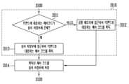
본 발명의 일 실시예에 따른 메모리 장치의 동작 방법은, 메모리 컨트롤러로부터 플레인 인터리브 동작을 지시하는 커맨드를 수신하는 단계; 상기 커맨드가 상기 메모리 컨트롤러의 첫 번째 커맨드인지 판단하는 단계; 상기 판단에 대한 응답으로, 복수의 제어 로직들이 공통적으로 접근 가능한 공통 저장부 또는 임시 저장부에 접근하여 상기 커맨드와 대응하는 제어 코드를 획득하는 단계; 상기 제어 코드를 상기 임시 저장부에 저장하는 단계; 및 상기 제어 코드에 기초하여 상기 플레인 인터리브 동작에 관한 제어 신호를 생성하는 단계를 포함할 수 있다.A method of operating a memory device according to one embodiment of the present invention may include: receiving a command instructing a plane interleave operation from a memory controller; determining whether the command is a first command of the memory controller; in response to the determination, accessing a common storage or a temporary storage commonly accessible to a plurality of control logics to obtain a control code corresponding to the command; storing the control code in the temporary storage; and generating a control signal related to the plane interleave operation based on the control code.
상기 임시 저장부는, 상기 제어 로직들이 병렬적으로 접근할 수 있도록 물리적으로 독립된 영역들을 포함할 수 있다.The above temporary storage unit may include physically independent areas so that the control logics can access them in parallel.
상기 제어 코드를 획득하는 단계는, 상기 커맨드가 상기 메모리 컨트롤러의 첫 번째 커맨드일 때, 상기 공통 저장부에 접근하여 상기 제어 코드를 획득할 수 있다.The step of obtaining the above control code can access the common storage to obtain the control code when the command is a first command of the memory controller.
상기 제어 코드를 획득하는 단계는, 상기 커맨드가 상기 메모리 컨트롤러의 첫 번째 커맨드가 아닐 때, 상기 공통 저장부 대신에 상기 임시 저장부에 접근하여 상기 제어 코드를 획득할 수 있다.The step of obtaining the above control code can obtain the control code by accessing the temporary storage instead of the common storage when the command is not the first command of the memory controller.
본 기술은 저장 공간을 효율적으로 활용할 수 있는 메모리 장치 및 그 동작 방법을 제공할 수 있다.The present technology can provide a memory device and its operating method capable of efficiently utilizing storage space.
도 1은 메모리 시스템을 설명하기 위한 도면이다.
도 2는 메모리 컨트롤러와 메모리 장치 사이에 교환되는 신호들을 설명하기 위한 도면이다.
도 3은 도 1의 메모리 장치를 구체적으로 설명하기 위한 도면이다.
도 4는 멀티 플레인 구조를 설명하기 위한 도면이다.
도 5는 도 4의 메모리 블록을 설명하기 위한 도면이다.
도 6은 도 4의 메모리 블록이 3차원으로 구성된 실시예를 설명하기 위한 도면이다.
도 7은 도 4의 메모리 블록이 3차원으로 구성된 다른 실시예를 설명하기 위한 도면이다.
도 8a 내지 도 8b는 도 4에 따른 멀티 플레인 구조를 갖는 메모리 장치의 플레인 인터리브 리드 동작을 나타내는 타이밍도이다.
도 9는 트리플 레벨 셀 형태의 메모리 셀들의 문턱전압 분포를 설명하기 위한 도면이다.
도 10은 도 4에 따른 멀티 플레인 구조를 갖는 메모리 장치에서 플레인 인터리브 리드 동작에 따른 제어 메모리의 활용 방법을 설명하기 위한 개념도이다.
도 11은 도 10에 따른 제어 메모리와 다른 형태로 제어 메모리를 구성하여 플레인 인터리브 리드 동작을 수행하는 방법을 설명하기 위한 개념도이다.
도 12는 도 11에 따른 제어 메모리 구성에서, 다른 커맨드를 수신하였을 때의 플레인 인터리브 리드 동작을 수행하는 방법을 설명하기 위한 개념도이다.
도 13은 도 10 내지 도 11에 따른 제어 메모리 구성을 갖는 메모리 장치의 동작 방법을 나타낸 예시 흐름도이다.
도 14는 도 13에 따른 단계 S110을 일부 구체화한 예시 흐름도이다.
도 15는 도 1의 메모리 컨트롤러를 구체적으로 설명하기 위한 도면이다.
도 16은 도 10 내지 도 11에 따른 제어 메모리 구성을 갖는 메모리 장치를 포함하는 메모리 시스템의 다른 실시 예를 설명하기 위한 도면이다.Figure 1 is a diagram explaining a memory system.
Figure 2 is a diagram for explaining signals exchanged between a memory controller and a memory device.
FIG. 3 is a drawing specifically explaining the memory device of FIG. 1.
Figure 4 is a drawing for explaining a multi-plane structure.
Figure 5 is a drawing for explaining the memory block of Figure 4.
FIG. 6 is a drawing for explaining an embodiment in which the memory block of FIG. 4 is configured in three dimensions.
FIG. 7 is a drawing for explaining another embodiment in which the memory block of FIG. 4 is configured in three dimensions.
FIGS. 8A and 8B are timing diagrams showing plane interleaved read operations of a memory device having a multi-plane structure according to FIG. 4.
Figure 9 is a drawing for explaining the threshold voltage distribution of memory cells in the triple-level cell form.
FIG. 10 is a conceptual diagram for explaining a method of utilizing control memory according to plane interleaved read operation in a memory device having a multi-plane structure according to FIG. 4.
FIG. 11 is a conceptual diagram for explaining a method of performing a plain interleaved read operation by configuring a control memory in a different form from the control memory according to FIG. 10.
FIG. 12 is a conceptual diagram for explaining a method of performing a plain interleaved read operation when another command is received in the control memory configuration according to FIG. 11.
FIG. 13 is an exemplary flowchart illustrating an operating method of a memory device having a control memory configuration according to FIGS. 10 and 11.
FIG. 14 is an exemplary flowchart partially specifying step S110 according to FIG. 13.
Figure 15 is a drawing specifically explaining the memory controller of Figure 1.
FIG. 16 is a drawing for explaining another embodiment of a memory system including a memory device having a control memory configuration according to FIGS. 10 and 11.
본 명세서 또는 출원에 개시되어 있는 본 발명의 개념에 따른 실시 예들에 대해서 특정한 구조적 내지 기능적 설명들은 단지 본 발명의 개념에 따른 실시 예를 설명하기 위한 목적으로 예시된 것으로, 본 발명의 개념에 따른 실시 예들은 다양한 형태로 실시될 수 있으며 본 명세서 또는 출원에 설명된 실시 예들에 한정되는 것으로 해석되어서는 아니 된다.Specific structural and functional descriptions of embodiments according to the concept of the present invention disclosed in this specification or application are merely exemplified for the purpose of explaining embodiments according to the concept of the present invention, and embodiments according to the concept of the present invention may be implemented in various forms and should not be construed as being limited to the embodiments described in this specification or application.
도 1은 메모리 시스템을 설명하기 위한 도면이다.Figure 1 is a diagram explaining a memory system.
도 1을 참조하면, 메모리 시스템(1000)은 데이터가 저장되는 메모리 장치(Memory Device; 1100), 메모리 시스템(1000)의 동작에 필요한 데이터를 임시로 저장하기 위한 버퍼 메모리(Buffer Memory; 1300), 및/또는 호스트(Host; 2000)의 제어에 따라 메모리 장치(1100) 및 버퍼 메모리(1300)를 제어하는 메모리 컨트롤러(Memory Controller; 1200)를 포함할 수 있다.Referring to FIG. 1, a memory system (1000) may include a memory device (Memory Device; 1100) in which data is stored, a buffer memory (Buffer Memory; 1300) for temporarily storing data required for the operation of the memory system (1000), and/or a memory controller (Memory Controller; 1200) that controls the memory device (1100) and the buffer memory (1300) under the control of a host (Host; 2000).
호스트(2000)는 USB (Universal Serial Bus), SATA (Serial AT Attachment), SAS (Serial Attached SCSI), HSIC (High Speed Interchip), SCSI (Small Computer System Interface), PCI (Peripheral Component Interconnection), PCIe (PCI express), NVMe (NonVolatile Memory express), UFS (Universal Flash Storage), SD (Secure Digital), MMC (MultiMedia Card), eMMC (embedded MMC), DIMM (Dual In-line Memory Module), RDIMM (Registered DIMM), LRDIMM (Load Reduced DIMM) 등과 같은 다양한 통신 방법들 중 적어도 하나를 이용하여 메모리 시스템(1000)과 통신할 수 있다.The host (2000) may communicate with the memory system (1000) using at least one of various communication methods, such as USB (Universal Serial Bus), SATA (Serial AT Attachment), SAS (Serial Attached SCSI), HSIC (High Speed Interchip), SCSI (Small Computer System Interface), PCI (Peripheral Component Interconnection), PCIe (PCI express), NVMe (NonVolatile Memory express), UFS (Universal Flash Storage), SD (Secure Digital), MMC (MultiMedia Card), eMMC (embedded MMC), DIMM (Dual In-line Memory Module), RDIMM (Registered DIMM), LRDIMM (Load Reduced DIMM), etc.
메모리 장치(1100)는 전원 공급이 차단되면 데이터가 소멸되는 휘발성 메모리 장치(Volatile Memory Device) 또는 전원 공급이 차단되더라도 데이터가 유지되는 비휘발성 메모리 장치(Non-volatile memory Device)로 구현될 수 있다. 메모리 장치(1100)는 메모리 컨트롤러(1200)의 제어에 따라 프로그램 동작, 리드 동작 또는 소거 동작을 수행할 수 있다. 예를 들면, 프로그램 동작 시, 메모리 장치(1100)는 메모리 컨트롤러(1200)로부터 커맨드, 어드레스 및 데이터를 입력받고 프로그램 동작을 수행할 수 있다. 리드 동작 시, 메모리 장치(1100)는 메모리 컨트롤러(1200)로부터 커맨드 및 어드레스를 입력받고, 리드된 데이터를 메모리 컨트롤러(1200)로 출력할 수 있다. 이를 위해, 메모리 장치(1100)는 데이터를 입출력하기 위한 입출력 회로를 포함할 수 있다.The memory device (1100) may be implemented as a volatile memory device in which data is lost when power is cut off, or a non-volatile memory device in which data is maintained even when power is cut off. The memory device (1100) may perform a program operation, a read operation, or an erase operation under the control of the memory controller (1200). For example, during a program operation, the memory device (1100) may receive a command, an address, and data from the memory controller (1200) and perform a program operation. During a read operation, the memory device (1100) may receive a command and an address from the memory controller (1200) and output the read data to the memory controller (1200). To this end, the memory device (1100) may include an input/output circuit for inputting and outputting data.
메모리 컨트롤러(1200)는 메모리 시스템(1000)의 동작을 전반적으로 제어하며, 호스트(2000)와 메모리 장치(1100) 사이의 데이터 교환을 제어할 수 있다. 예를 들어, 메모리 컨트롤러(1200)는 호스트(2000)의 요청에 따라 메모리 장치(1100)를 제어하여 데이터를 프로그램(program), 리드(read) 또는 소거(erase)할 수 있다. 또한, 메모리 컨트롤러(1200)는 호스트(2000)로부터 데이터와 논리 어드레스(logical address)를 입력 받고, 논리 어드레스를 메모리 장치(1100) 내에 데이터가 실제 저장될 영역을 가리키는 물리 어드레스(physical address)로 변환할 수 있다. 또한 메모리 컨트롤러(1200)은 논리 어드레스와 물리 어드레스 간의 맵핑(mapping) 관계를 구성하는 논리-물리 어드레스 맵핑 테이블(logical-to-physical address mapping table)을 버퍼 메모리(1300)에 저장할 수 있다.The memory controller (1200) controls the overall operation of the memory system (1000) and can control data exchange between the host (2000) and the memory device (1100). For example, the memory controller (1200) can control the memory device (1100) to program, read, or erase data according to a request of the host (2000). In addition, the memory controller (1200) can receive data and a logical address from the host (2000) and convert the logical address into a physical address that indicates an area in the memory device (1100) where the data is to be actually stored. In addition, the memory controller (1200) can store a logical-to-physical address mapping table that configures a mapping relationship between a logical address and a physical address in the buffer memory (1300).
메모리 장치(1100)는, 복수의 플레인들(planes)을 포함할 수 있다. 메모리 컨트롤러(1200)는, 호스트(2000)로부터의 요청(request)에 따라 복수의 플레인들(planes)에 대하여 병렬적으로(또는 인터리브하게) 프로그램 동작, 리드 동작 또는 소거 동작을 수행하도록 메모리 장치(1100)를 제어할 수 있다. 예를 들어, 메모리 컨트롤러(1200)는, 메모리 장치(1100)가 플레인 인터리브(plane interleave) 동작을 수행하도록 제어할 수 있다. 플레인 인터리브 동작은 플레인 인터리브 리드(plane interleave read) 동작을 포함할 수 있다. 메모리 컨트롤러(1200)는, 호스트(2000)로부터 수신되는 복수의 리드 요청들에 기초하여, 플레인 인터리브 리드 동작을 지시하는 리드 커맨드를 생성하고, 생성된 리드 커맨드를 메모리 장치(1100)로 출력할 수 있다. 예를 들어, 리드 커맨드는 플레인들 중 선택된 플레인의 물리 어드레스를 포함할 수 있다. 메모리 장치(1100)는 리드 커맨드에 기초하여 복수의 플랜들(planes) 각각이 인터리브하게 데이터를 리드하고, 리드된 데이터들을 메모리 컨트롤러(1200)로 전달할 수 있다. 이하에서는 플레인 인터리브 리드 동작을 중심으로 서술하지만, 반드시 이에 한정되는 것은 아니며, 메모리 장치(1100)가 복수의 칩들(chips) 또는 복수의 다이들(dies)을 포함하고, 칩이나 다이 단위로 인터리브 동작을 수행하는 것도 포함될 수 있다.The memory device (1100) may include a plurality of planes. The memory controller (1200) may control the memory device (1100) to perform a program operation, a read operation, or an erase operation in parallel (or interleaved) for the plurality of planes according to a request from the host (2000). For example, the memory controller (1200) may control the memory device (1100) to perform a plane interleave operation. The plane interleave operation may include a plane interleave read operation. The memory controller (1200) may generate a read command instructing a plane interleave read operation based on a plurality of read requests received from the host (2000), and output the generated read command to the memory device (1100). For example, the read command may include a physical address of a plane selected from among the planes. The memory device (1100) may read data interleavedly from each of a plurality of planes based on the read command, and transmit the read data to the memory controller (1200). The following description focuses on a plane interleaved read operation, but is not necessarily limited thereto, and may also include a case where the memory device (1100) includes a plurality of chips or a plurality of dies, and performs an interleaved operation on a chip or die basis.
버퍼 메모리(1300)는 메모리 컨트롤러(1200)의 동작 메모리 또는 캐시 메모리로 사용될 수 있으며, 상술한 정보 외에도 메모리 시스템(1000) 내에서 사용되는 시스템 데이터를 저장할 수 있다. 실시예에 따라, 버퍼 메모리(1300)는 DDR SDRAM(Double Data Rate Synchronous Dynamic Random Access Memory), DDR4 SDRAM, LPDDR4(Low Power Double Data Rate4) SDRAM, GDDR(Graphics Double Data Rate) SDRAM, LPDDR(Low Power DDR) 또는 RDRAM(Rambus Dynamic Random Access Memory)을 포함할 수 있다.The buffer memory (1300) can be used as an operating memory or cache memory of the memory controller (1200), and can store system data used within the memory system (1000) in addition to the above-described information. According to an embodiment, the buffer memory (1300) can include DDR SDRAM (Double Data Rate Synchronous Dynamic Random Access Memory), DDR4 SDRAM, LPDDR4 (Low Power Double Data Rate4) SDRAM, GDDR (Graphics Double Data Rate) SDRAM, LPDDR (Low Power DDR), or RDRAM (Rambus Dynamic Random Access Memory).
도 2는 메모리 컨트롤러와 메모리 장치 사이에 교환되는 신호들을 설명하기 위한 도면이다.Figure 2 is a diagram for explaining signals exchanged between a memory controller and a memory device.
도 2를 참조하면, 메모리 컨트롤러(1200)와 메모리 장치(1100)는 입출력 패드(DQ)를 통해 커맨드, 데이터 및/또는 어드레스를 서로 주고받을 수 있다.Referring to FIG. 2, the memory controller (1200) and the memory device (1100) can exchange commands, data, and/or addresses with each other through input/output pads (DQ).
메모리 장치(1100)는 CE# 패드를 통해 칩 인에이블 신호를 수신하고, WE# 패드를 통해 라이트 인에이블 신호를 수신하고, RE# 패드를 통해 리드 인에이블 신호를 수신하고, ALE 패드를 통해 어드레스 래치 인에이블 신호를 수신하고, CLE 패드를 통해 커맨드 래치 인에이블 신호를 수신하고, WP# 패드를 통해 라이트 프로텍션 신호를 수신할 수 있다.The memory device (1100) can receive a chip enable signal through the CE# pad, a write enable signal through the WE# pad, a read enable signal through the RE# pad, an address latch enable signal through the ALE pad, a command latch enable signal through the CLE pad, and a write protection signal through the WP# pad.
또한, 메모리 장치(1100)는 RB 패드를 통해 레디비지 신호를 메모리 컨트롤러(1200)로 출력할 수 있다. 예를 들어, 메모리 장치(1100)가 복수의 플레인들을 포함하는 경우, 메모리 장치(1100)는 각각의 플레인들이 레디 상태와 비지 상태 중 어느 상태에 있는지를 지시하는 복수의 레디비지 신호들을 출력할 수 있다.Additionally, the memory device (1100) can output a ready busy signal to the memory controller (1200) through the RB pad. For example, when the memory device (1100) includes a plurality of planes, the memory device (1100) can output a plurality of ready busy signals that indicate which state each of the planes is in among a ready state and a busy state.
도 3은 도 1의 메모리 장치를 구체적으로 설명하기 위한 도면이다.FIG. 3 is a drawing specifically explaining the memory device of FIG. 1.
도 3을 참조하면, 메모리 장치(1100)는 휘발성 메모리 장치 또는 비휘발성 메모리 장치로 구현될 수 있고, 도 3에는 비휘발성 메모리 장치가 실시예로써 도시되어 있으나, 본 실시예는 비휘발성 메모리 장치로 제한되지는 않는다.Referring to FIG. 3, the memory device (1100) may be implemented as a volatile memory device or a nonvolatile memory device, and although a nonvolatile memory device is illustrated as an example in FIG. 3, the present embodiment is not limited to a nonvolatile memory device.
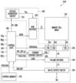
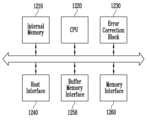
메모리 장치(1100)는 데이터가 저장되는 메모리 셀 어레이(100)를 포함할 수 있다. 메모리 장치(1100)는 메모리 셀 어레이(100)에 데이터를 저장하기 위한 프로그램 동작(program operation), 저장된 데이터를 출력하기 위한 리드 동작(read operation) 및 저장된 데이터를 소거하기 위한 소거 동작(erase operation)을 수행하도록 구성된 주변 회로들(peripheral circuits; 200)을 포함할 수 있다. 메모리 장치(1100)는 메모리 컨트롤러(1200)의 제어에 따라 주변 회로들(200)을 제어하는 제어 로직(300)을 포함할 수 있다.A memory device (1100) may include a memory cell array (100) in which data is stored. The memory device (1100) may include peripheral circuits (200) configured to perform a program operation for storing data in the memory cell array (100), a read operation for outputting the stored data, and an erase operation for erasing the stored data. The memory device (1100) may include control logic (300) that controls the peripheral circuits (200) under the control of a memory controller (1200).
메모리 셀 어레이(100)는 데이터가 저장되는 다수의 메모리 셀들을 포함한다. 예를 들면, 메모리 셀 어레이(100)는 적어도 하나의 플레인(plane)을 포함할 수 있고, 플레인은 하나 이상의 메모리 블록들(memory blocks)을 포함할 수 있다. 실시 예에서, 플레인은 프로그램, 리드 또는 소거 동작을 수행시에 엑세스되는 메모리 영역의 단위일 수 있다. 메모리 블록들 각각은 다수의 메모리 셀들을 포함할 수 있다. 다수의 플레인들이 포함된 구조를 멀티 플레인 구조로 지칭할 수 있다. 메모리 블록들에는 사용자 데이터(user data) 및 메모리 장치(1100)의 동작에 필요한 정보가 저장될 수 있다. 메모리 블록들은 2차원 또는 3차원 구조로 구현될 수 있다. 2차원 구조를 가지는 메모리 블록들은 기판에 평행하게 배열된 메모리 셀들을 포함할 수 있고, 3차원 구조를 가지는 메모리 블록들은 기판에 수직하게 적층된 메모리 셀들을 포함할 수 있다.The memory cell array (100) includes a plurality of memory cells in which data is stored. For example, the memory cell array (100) may include at least one plane, and the plane may include one or more memory blocks. In an embodiment, a plane may be a unit of a memory area accessed when performing a program, read, or erase operation. Each of the memory blocks may include a plurality of memory cells. A structure including a plurality of planes may be referred to as a multi-plane structure. User data and information necessary for the operation of the memory device (1100) may be stored in the memory blocks. The memory blocks may be implemented in a two-dimensional or three-dimensional structure. Memory blocks having a two-dimensional structure may include memory cells arranged parallel to a substrate, and memory blocks having a three-dimensional structure may include memory cells stacked vertically on a substrate.
주변 회로들(200)은, 제어 로직(300)의 제어에 따라 프로그램, 리드 및 소거 동작을 수행하도록 구성될 수 있다. 예를 들면, 주변 회로들(200)은 전압 생성 회로(VOLTAGE GENERATION CIRCUIT; 210), 로우 디코더(ROW DECODER; 220), 페이지 버퍼 그룹(PAGE BUFFER GROUP; 230), 컬럼 디코더(COLUMN DECODER; 240), 입출력 회로(INPUT/OUTPUT CIRCUIT; 250) 및 전류 센싱 회로(CURRENT SENSING CIRCUIT; 260), 제어 메모리(CONTROL MEMORY; 270)를 포함할 수 있다.The peripheral circuits (200) may be configured to perform program, read, and erase operations under the control of the control logic (300). For example, the peripheral circuits (200) may include a voltage generation circuit (VOLTAGE GENERATION CIRCUIT; 210), a row decoder (ROW DECODER; 220), a page buffer group (PAGE BUFFER GROUP; 230), a column decoder (COLUMN DECODER; 240), an input/output circuit (INPUT/OUTPUT CIRCUIT; 250), a current sensing circuit (CURRENT SENSING CIRCUIT; 260), and a control memory (CONTROL MEMORY; 270).
전압 생성 회로(210)는, 제어 로직(300)에서 출력되는 동작 신호(OP_CMD)에 응답하여 프로그램, 리드 및 소거 동작들에 사용되는 다양한 동작 전압들(Vop)을 생성할 수 있다. 예를 들면, 전압 생성 회로(210)는 제어 로직(300)의 제어에 따라, 프로그램 전압, 검증 전압, 패스 전압, 리드 전압, 소거 전압 등의 다양한 전압들을 생성할 수 있다.The voltage generation circuit (210) can generate various operating voltages (Vop) used for program, read, and erase operations in response to an operating signal (OP_CMD) output from the control logic (300). For example, the voltage generation circuit (210) can generate various voltages such as a program voltage, a verification voltage, a pass voltage, a read voltage, and an erase voltage under the control of the control logic (300).
로우 디코더(220)는, 제어 로직(300)으로부터 출력된 로우 어드레스(RADD)에 응답하여, 메모리 셀 어레이(100)의 메모리 블록들 중 선택된 메모리 블록에 연결된 로컬 라인들(local lines; LL)에 동작 전압들(Vop)을 공급할 수 있다. 로컬 라인들(LL)은 로컬 워드 라인들(local word lines), 로컬 드레인 셀렉트 라인들(local drain select lines), 및/또는 로컬 소스 셀렉트 라인들(local source select lines)을 포함할 수 있다. 이 외에도, 로컬 라인들(LL)은 소스 라인(source line)과 같이 메모리 블록에 연결된 다양한 라인들을 포함할 수 있다.The row decoder (220) can supply operating voltages (Vop) to local lines (LL) connected to a selected memory block among the memory blocks of the memory cell array (100) in response to a row address (RADD) output from the control logic (300). The local lines (LL) can include local word lines, local drain select lines, and/or local source select lines. In addition, the local lines (LL) can include various lines connected to the memory block, such as a source line.
페이지 버퍼 그룹(230)은, 메모리 셀 어레이(100)의 메모리 블록들에 연결된 비트 라인들(BL1~BLI)에 연결될 수 있다. 페이지 버퍼 그룹(230)은 비트 라인들(BL1~BLI)에 연결된 다수의 페이지 버퍼들(PB1~PBI)을 포함할 수 있다. 페이지 버퍼들(PB1~PBI)은 제어 로직(300)으로부터 출력된 페이지 버퍼 제어 신호들(PBSIGNALS)에 응답하여 동작할 수 있다. 예를 들면, 페이지 버퍼들(PB1~PBI)은 비트 라인들(BL1~BLI)을 통해 수신된 데이터를 임시로 저장하거나, 리드 또는 검증 동작 시, 비트 라인들(BL1~BLI)의 전압 또는 전류를 센싱(sensing)할 수 있다.The page buffer group (230) may be connected to bit lines (BL1 to BLI) connected to memory blocks of the memory cell array (100). The page buffer group (230) may include a plurality of page buffers (PB1 to PBI) connected to the bit lines (BL1 to BLI). The page buffers (PB1 to PBI) may operate in response to page buffer control signals (PBSIGNALS) output from the control logic (300). For example, the page buffers (PB1 to PBI) may temporarily store data received through the bit lines (BL1 to BLI), or sense the voltage or current of the bit lines (BL1 to BLI) during a read or verify operation.
컬럼 디코더(240)는, 제어 로직(300)으로부터 출력된 컬럼 어드레스(CADD)에 응답하여 입출력 회로(250)와 페이지 버퍼 그룹(230) 사이에서 데이터를 전달할 수 있다. 예를 들면, 컬럼 디코더(240)는 데이터 라인들(DL)을 통해 페이지 버퍼들(PB1~PBI)과 데이터를 주고받거나, 컬럼 라인들(CL)을 통해 입출력 회로(250)와 데이터를 주고받을 수 있다.The column decoder (240) can transfer data between the input/output circuit (250) and the page buffer group (230) in response to the column address (CADD) output from the control logic (300). For example, the column decoder (240) can transfer data to and from the page buffers (PB1 to PBI) through the data lines (DL), or transfer data to and from the input/output circuit (250) through the column lines (CL).
입출력 회로(250)는, 입출력 패드(DQ)를 통해 메모리 컨트롤러(1200)로부터 커맨드(CMD), 어드레스(ADD) 및 데이터를 수신할 수 있고, 리드된 데이터를 입출력 패드(DQ)를 통해 메모리 컨트롤러(1200)로 출력할 수 있다. 예를 들어, 입출력 회로(250)는 메모리 컨트롤러(1200)로부터 수신된 커맨드(CMD) 및 어드레스(ADD)를 제어 로직(300)에 전달하거나, 데이터(DATA)를 컬럼 디코더(240)와 주고받을 수 있다.The input/output circuit (250) can receive a command (CMD), an address (ADD), and data from the memory controller (1200) through the input/output pad (DQ), and can output the read data to the memory controller (1200) through the input/output pad (DQ). For example, the input/output circuit (250) can transfer the command (CMD) and address (ADD) received from the memory controller (1200) to the control logic (300), or exchange data (DATA) with the column decoder (240).
전류 센싱 회로(260)는 리드 동작(read operation) 또는 검증 동작(verify operation)시, 허용 비트(VRY_BIT<#>)에 응답하여 기준 전류를 생성하고, 페이지 버퍼 그룹(230)으로부터 수신된 센싱 전압(VPB)과 기준 전류에 의해 생성된 기준 전압을 비교하여 패스 신호(PASS) 또는 페일 신호(FAIL)를 출력할 수 있다.The current sensing circuit (260) can generate a reference current in response to an allow bit (VRY_BIT<#>) during a read operation or a verify operation, and compare a sensing voltage (VPB) received from the page buffer group (230) with a reference voltage generated by the reference current to output a pass signal (PASS) or a fail signal (FAIL).
제어 로직(300)은 CE#, WE#, RE#, ALE, CLE 및 WP# 패드들을 통해 수신되는 신호들에 응답하여 커맨드(CMD) 및 어드레스(ADD)를 수신할 수 있다. 제어 로직(300)은 커맨드(CMD) 및 어드레스(ADD)를 수신한 것에 대한 응답으로, 제어 코드(CTRCODES)를 참조하여, 주변 회로들(200)를 제어하기 위한 제어 신호들을 생성하고, 생성된 제어 신호들을 주변 회로들(200)로 출력할 수 있다. 예를 들어, 제어 신호들은, 동작 신호(OP_CMD), 로우 어드레스(RADD), 페이지 버퍼 제어 신호들(PBSIGNALS) 및 허용 비트(VRY_BIT<#>) 중 적어도 하나를 포함할 수 있다. 제어 로직(300)은, 동작 신호(OP_CMD)를 전압 생성 회로(210)로 출력하고, 로드 어드레스(RADD)를 로우 디코더(220)로 출력하고, 페이지 버퍼 제어 신호들(PBSIGNALS)를 페이지 버퍼 그룹(230)으로 출력하고, 허용 비트(VRY_BIT<#>)를 전류 센싱 회로(260)로 출력할 수 있다. 또한, 제어 로직(300)은 패스 신호(PASS) 또는 페일 신호(FAIL)에 응답하여 검증 동작이 패스 또는 페일 되었는지를 판단할 수 있다.The control logic (300) can receive a command (CMD) and an address (ADD) in response to signals received through the CE#, WE#, RE#, ALE, CLE, and WP# pads. In response to receiving the command (CMD) and the address (ADD), the control logic (300) can generate control signals for controlling the peripheral circuits (200) with reference to the control code (CTRCODES), and output the generated control signals to the peripheral circuits (200). For example, the control signals can include at least one of an operation signal (OP_CMD), a row address (RADD), page buffer control signals (PBSIGNALS), and a permission bit (VRY_BIT<#>). The control logic (300) can output an operation signal (OP_CMD) to a voltage generation circuit (210), output a load address (RADD) to a row decoder (220), output page buffer control signals (PBSIGNALS) to a page buffer group (230), and output an allowance bit (VRY_BIT<#>) to a current sensing circuit (260). In addition, the control logic (300) can determine whether a verification operation has passed or failed in response to a pass signal (PASS) or a fail signal (FAIL).
제어 메모리(270)는, 제어 로직(300)이 주변 회로(200)를 제어하기 위한 제어 코드(CTRCODES)를 저장할 수 있다. 제어 코드는 프로그램 동작, 리드 동작, 소거 동작 등에 관한 제어 신호를 생성하기 위한 코드(또는 알고리즘), 플레인 인터리브 동작에 관한 제어 신호를 생성하기 위한 코드를 포함할 수 있다. 예를 들어, 제어 코드는 플레인 인터리브 리드 동작에 관한 제어 신호를 생성하기 위한 코드를 포함할 수 있다. 예를 들어, 제어 메모리(270)는, 롬(Read Only Memory; ROM), PROM (Programmable ROM), EPROM (Electrically Programmable ROM), EEPROM (Electrically Erasable and Programmable ROM) 등일 수 있다. 제어 메모리(270)는 표현하기에 따라 주변 회로들(200)에 포함되는 것으로 해석될 수 있으나, 설명을 위해 또는 지칭하는 대상을 분명히 하기 위해 주변 회로들(200)과 구별될 수도 있다.The control memory (270) can store control codes (CTRCODES) for the control logic (300) to control the peripheral circuits (200). The control codes can include codes (or algorithms) for generating control signals for a program operation, a read operation, an erase operation, etc., and codes for generating control signals for a plane interleaved operation. For example, the control codes can include codes for generating control signals for a plane interleaved read operation. For example, the control memory (270) can be a Read Only Memory (ROM), a PROM (Programmable ROM), an EPROM (Electrically Programmable ROM), an EEPROM (Electrically Erasable and Programmable ROM), etc. The control memory (270) can be interpreted as being included in the peripheral circuits (200) depending on the expression, but can also be distinguished from the peripheral circuits (200) for the purpose of explanation or to clarify the target referred to.
도 4는 멀티 플레인 구조를 설명하기 위한 도면이다.Figure 4 is a drawing for explaining a multi-plane structure.
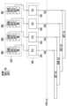
도 4를 참조하면, 멀티 플레인 구조를 가지는 메모리 장치(1100)는 다수의 플레인들(P1~P4)을 포함할 수 있다. 예를 들면 제1 내지 제4 플레인들(P1~P4)이 하나의 메모리 장치(1100)에 포함될 수 있다.Referring to FIG. 4, a memory device (1100) having a multi-plane structure may include a plurality of planes (P1 to P4). For example, the first to fourth planes (P1 to P4) may be included in one memory device (1100).
제1 내지 제4 플레인들(P1~P4) 각각은 로우 디코더들(RD1~RD4) 및 페이지 버퍼 그룹들(PBG1~PBG4)이 연결될 수 있으며, 각각 독립적으로 동작할 수 있다. 예를 들면, 제1 플레인(P1)은 제1 로우 디코더(RD1) 및 제1 페이지 버퍼 그룹(PBG1)에 연결되어 동작할 수 있고, 제2 플레인(P2)은 제2 로우 디코더(RD2) 및 제2 페이지 버퍼 그룹(PBG2)에 연결되어 동작할 수 있고, 제3 플레인(P3)은 제3 로우 디코더(RD3) 및 제3 페이지 버퍼 그룹(PB3)에 연결되어 동작할 수 있고, 제4 플레인(P4)은 제4 로우 디코더(RD4) 및 제4 페이지 버퍼 그룹(PB4)에 연결되어 동작할 수 있다.Each of the first to fourth planes (P1 to P4) can be connected to row decoders (RD1 to RD4) and page buffer groups (PBG1 to PBG4) and can operate independently. For example, the first plane (P1) can be connected to the first row decoder (RD1) and the first page buffer group (PBG1) and can operate, the second plane (P2) can be connected to the second row decoder (RD2) and the second page buffer group (PBG2) and can operate, the third plane (P3) can be connected to the third row decoder (RD3) and the third page buffer group (PB3) and can operate, and the fourth plane (P4) can be connected to the fourth row decoder (RD4) and the fourth page buffer group (PB4) and can operate.
리드 동작을 예를 들면, 제1 내지 제4 로우 디코더들(RD1~RD4)은 각각 수신된 로우 어드레스에 응답하여 제1 내지 제4 플레인들(P1~P4) 각각에서 선택된 메모리 블록에 리드 전압을 인가할 수 있다. 제1 내지 제4 페이지 버퍼 그룹들(PBG1~PBG4)은 제1 내지 제4 플레인들(P1~P4)에 연결된 비트 라인들의 전압 또는 전류를 센싱하여 리드된 데이터를 임시로 저장할 수 있다. 제1 내지 제4 플레인들(P1~P4)의 센싱 동작이 모두 완료되면, 제1 내지 제4 페이지 버퍼 그룹들(PBG1~PBG4)에 임시로 저장된 리드된 데이터는 입출력 회로(도 2의 250)를 통해 순차적으로 출력될 수 있다. 예를 들면, 제1 페이지 버퍼 그룹(PBG1)의 리드된 데이터가 첫 번째로 출력된 후, 제2 내지 제4 페이지 버퍼 그룹들(PBG2~PBG4)의 리드된 데이터가 순차적으로 출력될 수 있다.For example, in a read operation, the first to fourth row decoders (RD1 to RD4) may apply a read voltage to a memory block selected from each of the first to fourth planes (P1 to P4) in response to a received row address, respectively. The first to fourth page buffer groups (PBG1 to PBG4) may sense voltages or currents of bit lines connected to the first to fourth planes (P1 to P4) to temporarily store the read data. When the sensing operations of the first to fourth planes (P1 to P4) are all completed, the read data temporarily stored in the first to fourth page buffer groups (PBG1 to PBG4) may be sequentially output through an input/output circuit (250 of FIG. 2). For example, after the read data of the first page buffer group (PBG1) is output first, the read data of the second to fourth page buffer groups (PBG2 to PBG4) can be output sequentially.
도 4에서와 같이 복수의 플레인들(P1~P4)을 포함하는 메모리 장치(1100)는, 서로 다른 플레인에 위치한 블록들이나 페이지들에 대하여 동시에 리드, 프로그램 또는 소거 동작을 수행할 수 있다. 예를 들어, 메모리 컨트롤러(1200)는, 제어 로직(300)에 플레인 인터리브 동작을 지시하는 커맨드를 전송할 수 있다. 더욱 상세하게, 메모리 컨트롤러(1200)는, 서로 다른 플레인에 위치한 블록들이나 페이지들에 대하여 동시에 리드하도록, 제어 로직(300)에 플레인 인터리브 리드 동작을 지시하는 커맨드를 전송할 수 있다.A memory device (1100) including a plurality of planes (P1 to P4) as shown in FIG. 4 can perform read, program, or erase operations simultaneously on blocks or pages located on different planes. For example, the memory controller (1200) can transmit a command instructing a plane interleave operation to the control logic (300). More specifically, the memory controller (1200) can transmit a command instructing a plane interleave read operation to the control logic (300) so as to simultaneously read blocks or pages located on different planes.
한편, 플레인 인터리브 동작을 수행하기 위해서 제어 로직(300)은, 플레인들(P1~P4) 각각에 상응하는 독립적인 제어 로직들(CL1~CL4)을 포함할 수 있다. 예를 들어, 제1 제어 로직(CL1)은 제1 플레인(P1)에 대한 동작을 제어할 수 있고, 제2 제어 로직(CL2)은 제2 플레인(P2)에 대한 동작을 제어할 수 있고, 제3 제어 로직(CL3)은 제3 플레인(P3)에 대한 동작을 제어할 수 있고, 제4 제어 로직(CL4)은 제4 플레인(P4)에 대한 동작을 제어할 수 있다. 따라서, 제1 내지 제4 로우 디코더들(RD1~RD4)과 제1 내지 제4 페이지 버퍼들(PBG1~PBG4)은 제1 내지 제4 제어 로직들(CL1~CL4)에 의해 각각 독립적으로 제어될 수 있다.Meanwhile, in order to perform the plane interleave operation, the control logic (300) may include independent control logics (CL1 to CL4) corresponding to each of the planes (P1 to P4). For example, the first control logic (CL1) may control the operation for the first plane (P1), the second control logic (CL2) may control the operation for the second plane (P2), the third control logic (CL3) may control the operation for the third plane (P3), and the fourth control logic (CL4) may control the operation for the fourth plane (P4). Accordingly, the first to fourth row decoders (RD1 to RD4) and the first to fourth page buffers (PBG1 to PBG4) may be independently controlled by the first to fourth control logics (CL1 to CL4), respectively.
또한, 제어 로직들(CL1~CL4)이 하나의 제어 메모리(270)를 사용할 경우, 플레인들(P1~P4) 사이의 독립적인 동작을 방해하는 병목현상이 발생할 수 있다. 예를 들어, 제1 제어 로직(CL1)이 제어 메모리에 접근하여 제어 코드를 획득하는 동안, 제어 메모리(270)는 비지 상태에 있기 때문에, 제2 제어 로직(CL2)이 제어 메모리(270)에 접근하여 제어 코드를 획득하는 것이 제한될 수 있다. 이러한 문제를 해결하기 위하여 제어 메모리(270)는 서로 독립된 복수의 제어 메모리들(CM1~CM4)을 포함할 수 있다. 예를 들어, 제1 제어 로직(CL1)은 제1 제어 메모리(CM1)를 참조하여 제어 코드를 획득하고, 제2 제어 로직(CL2)은 제2 제어 메모리(CM2)를 참조하여 제어 코드를 획득하고, 제3 제어 로직(CL3)은 제3 제어 메모리(CM3)를 참조하여 제어 코드를 획득하고, 제4 제어 로직(CL4)은 제4 제어 메모리(CM4)를 참조하여 제어 코드를 획득할 수 있다.In addition, when the control logics (CL1 to CL4) use one control memory (270), a bottleneck phenomenon may occur that hinders independent operations between the planes (P1 to P4). For example, while the first control logic (CL1) accesses the control memory to obtain a control code, the control memory (270) is in a busy state, so the second control logic (CL2) may be restricted from accessing the control memory (270) to obtain the control code. To solve this problem, the control memory (270) may include a plurality of independent control memories (CM1 to CM4). For example, the first control logic (CL1) can obtain a control code by referencing the first control memory (CM1), the second control logic (CL2) can obtain a control code by referencing the second control memory (CM2), the third control logic (CL3) can obtain a control code by referencing the third control memory (CM3), and the fourth control logic (CL4) can obtain a control code by referencing the fourth control memory (CM4).
이하에서는, 도 4와 같이 플레인들(P1~P4)마다 독립된 제어 로직(CL1~CL4)이 있는 것으로 전제로 설명하지만 반드시 이에 한정되는 것은 아니다. 예를 들어, 제어 로직들(CL1~CL4) 중 적어도 일부가 통합되어 하나의 제어 로직이 2개 이상의 플레인들을 제어하도록 구현될 수도 있다. 또한, 후술하는 실시예에서는 제어 메모리들(CM1~CM4)이 통합되어 하나의 제어 메모리가 2개 이상의 플레인 제어를 위한 제어 코드를 저장하도록 구현될 수도 있다.Hereinafter, it is assumed that each of the planes (P1 to P4) has an independent control logic (CL1 to CL4) as shown in Fig. 4, but it is not necessarily limited thereto. For example, at least some of the control logics (CL1 to CL4) may be integrated so that one control logic controls two or more planes. In addition, in the embodiment described below, the control memories (CM1 to CM4) may be integrated so that one control memory stores control codes for controlling two or more planes.
도 5는 도 4의 메모리 블록을 설명하기 위한 도면이다.Figure 5 is a drawing for explaining the memory block of Figure 4.
도 5를 참조하면, 도 4에 도시된 다수의 메모리 블록들(BLK1~BLK6) 중에서 제1 메모리 블록(BLK1)이 예시적으로 도시된다. 나머지 메모리 블록들(BLK2~BLK6)은 제1 메모리 블록(BLK1)과 동일한 형태를 가질 수 있다.Referring to FIG. 5, a first memory block (BLK1) among a plurality of memory blocks (BLK1 to BLK6) illustrated in FIG. 4 is illustrated as an example. The remaining memory blocks (BLK2 to BLK6) may have the same shape as the first memory block (BLK1).
제1 메모리 블록(BLK1)은 비트 라인들(BL1~BLI)과 소스 라인(source line; SL) 사이에 연결된 다수의 셀 스트링들(cell strings; ST)을 포함할 수 있다. 예를 들면, 셀 스트링들(ST)은 비트 라인들(BL1~BLI)에 각각 연결되고, 소스 라인(SL)에 공통으로 연결될 수 있다. 셀 스트링들(ST)은 서로 유사하게 구성되므로, 이 중 제1 비트 라인(BL1)에 연결된 셀 스트링(ST)을 예를 들어 설명하면 다음과 같다.The first memory block (BLK1) may include a plurality of cell strings (ST) connected between bit lines (BL1 to BLI) and a source line (SL). For example, the cell strings (ST) may be connected to the bit lines (BL1 to BLI), respectively, and may be commonly connected to the source line (SL). Since the cell strings (ST) are configured similarly to each other, an example of a cell string (ST) connected to the first bit line (BL1) will be described as follows.
셀 스트링(ST)은 소스 라인(SL)과 제1 비트 라인(BL1) 사이에서 서로 직렬로 연결된 소스 셀렉트 트랜지스터(source select transistor; SST), 제1 내지 제n 메모리 셀들(memory cells; F1~Fn; n은 양의 정수) 및 드레인 셀렉트 트랜지스터(drain select transistor; DST)를 포함할 수 있다. 소스 및 드레인 셀렉트 트랜지스터들(SST 및 DST)의 개수는 도 5에 도시된 개수로 한정되지 않는다. 소스 셀렉트 트랜지스터(SST)는 소스 라인(SL)과 제1 메모리 셀(F1) 사이에 연결될 수 있다. 제1 내지 제n 메모리 셀들(F1~Fn)은 소스 셀렉트 트랜지스터(SST)와 드레인 셀렉트 트랜지스터(DST) 사이에서 서로 직렬로 연결될 수 있다. 드레인 셀렉트 트랜지스터(DST)는 제n 메모리 셀(Fn)과 제1 비트 라인(BL1) 사이에 연결될 수 있다. 도면에는 도시되지 않았으나, 메모리 셀들(F1~Fn) 사이 또는 소스 셀렉트 트랜지스터(SST)와 드레인 셀렉트 트랜지스터(DST) 사이에 더미 셀들(dummy cells)이 더 연결될 수도 있다.A cell string (ST) may include a source select transistor (SST), first to n-th memory cells (memory cells; F1 to Fn; n is a positive integer), and a drain select transistor (DST) connected in series between a source line (SL) and a first bit line (BL1). The number of source and drain select transistors (SST and DST) is not limited to the number shown in FIG. 5. The source select transistor (SST) may be connected between the source line (SL) and the first memory cell (F1). The first to n-th memory cells (F1 to Fn) may be connected in series between the source select transistor (SST) and the drain select transistor (DST). The drain select transistor (DST) may be connected between the n-th memory cell (Fn) and the first bit line (BL1). Although not shown in the drawing, dummy cells may be additionally connected between the memory cells (F1 to Fn) or between the source select transistor (SST) and the drain select transistor (DST).
서로 다른 셀 스트링들(ST)에 포함된 소스 셀렉트 트랜지스터들(SST)의 게이트들은 소스 셀렉트 라인(source select line; SSL)에 연결될 수 있고, 제1 내지 제n 메모리 셀들(F1~Fn)의 게이트들은 제1 내지 제n 워드라인들(word lines; WL1~WLn)에 연결될 수 있고, 드레인 셀렉트 트랜지스터들(DST)의 게이트들은 드레인 셀렉트 라인들(drain select lines; DSL)에 연결될 수 있다. 여기서, 워드 라인들(WL1~WLn) 각각에 연결된 메모리 셀들의 그룹을 페이지(page; PG)라 한다. 예를 들면, 서로 다른 셀 스트링들(ST)에 포함된 메모리 셀들(F1~Fn) 중 제1 워드 라인(WL1)에 연결된 제1 메모리 셀들(F1)의 그룹이 하나의 물리 페이지(physical page; PPG)가 될 수 있다. 프로그램 및 리드 동작들은 물리 페이지(PPG) 단위로 수행될 수 있다.Gates of source select transistors (SST) included in different cell strings (ST) can be connected to source select lines (SSL), gates of first to n-th memory cells (F1 to Fn) can be connected to first to n-th word lines (WL1 to WLn), and gates of drain select transistors (DST) can be connected to drain select lines (DSL). Here, a group of memory cells connected to each of the word lines (WL1 to WLn) is called a page (PG). For example, a group of first memory cells (F1) connected to a first word line (WL1) among the memory cells (F1 to Fn) included in different cell strings (ST) can become one physical page (PPG). Program and read operations can be performed in units of physical pages (PPG).
도 6은 도 4의 메모리 블록이 3차원으로 구성된 실시예를 설명하기 위한 도면이다.FIG. 6 is a drawing for explaining an embodiment in which the memory block of FIG. 4 is configured in three dimensions.
도 6을 참조하면, 도 4에 도시된 다수의 메모리 블록들(BLK1~BLK6) 중에서 제1 메모리 블록(BLK1)이 예시적으로 도시된다. 나머지 메모리 블록들(BLK2~BLK6)은 제1 메모리 블록(BLK1)과 동일한 형태를 가질 수 있다.Referring to FIG. 6, a first memory block (BLK1) among a plurality of memory blocks (BLK1 to BLK6) illustrated in FIG. 4 is illustrated as an example. The remaining memory blocks (BLK2 to BLK6) may have the same shape as the first memory block (BLK1).
3차원 구조로 구현된 제1 메모리 블록(BLK1)은 기판 상에 수직한(Z 방향) I자 형태로 형성될 수 있으며, 비트 라인들(BL)과 소스 라인(SL) 사이에 배열된 다수의 셀 스트링들(ST)을 포함할 수 있다. 또는, 소스 라인(SL) 대신 웰(well)이 형성될 수도 있다. 이러한 구조를 BiCS(Bit Cost Scalable)라고 부르기도 한다. 예를 들면, 소스 라인(SL)이 기판의 상부에 수평하게 형성된 경우, BiCS 구조를 갖는 셀 스트링들(ST)은 소스 라인(SL)의 상부에 수직한 방향(Z 방향)으로 형성될 수 있다.A first memory block (BLK1) implemented with a three-dimensional structure may be formed in an I-shape vertically (in the Z direction) on a substrate, and may include a plurality of cell strings (ST) arranged between bit lines (BL) and source lines (SL). Alternatively, a well may be formed instead of the source line (SL). This structure is also called BiCS (Bit Cost Scalable). For example, when the source line (SL) is formed horizontally on the upper portion of the substrate, the cell strings (ST) having the BiCS structure may be formed in a direction vertically (in the Z direction) to the upper portion of the source line (SL).
더욱 구체적으로 설명하면, 셀 스트링들(ST)은 제1 방향(X 방향) 및 제2 방향(Y 방향)으로 각각 배열될 수 있다. 셀 스트링들(ST)은 서로 이격되어 적층된 소스 셀렉트 라인들(SSL), 워드 라인들(WL) 및 드레인 셀렉트 라인들(DSL)을 포함할 수 있다. 소스 셀렉트 라인들(SSL), 워드 라인들(WL) 및 드레인 셀렉트 라인들(DSL)의 개수는 도면에 도시된 개수에 한정되지 않으며, 메모리 장치에 따라 다를 수 있다. 셀 스트링들(ST)은 소스 셀렉트 라인들(SSL), 워드라인들(WL) 및 드레인 셀렉트 라인들(DSL)을 수직으로 관통하는 수직 채널막들(CH)과, 드레인 셀렉트 라인들(DSL)의 상부로 돌출된 수직 채널막들(CH)의 상부에 접하며 제2 방향(Y 방향)으로 연장된 비트 라인들(BL)을 포함할 수 있다. 메모리 셀들은 워드 라인들(WL)과 수직 채널막들(CH) 사이에 형성될 수 있다. 비트 라인들(BL)과 수직 채널막들(CH) 사이에는 콘택 플러그(CT)가 더 형성될 수도 있다.More specifically, the cell strings (ST) may be arranged in a first direction (X direction) and a second direction (Y direction), respectively. The cell strings (ST) may include source select lines (SSL), word lines (WL), and drain select lines (DSL) that are spaced apart from each other and stacked. The number of the source select lines (SSL), word lines (WL), and drain select lines (DSL) is not limited to the number illustrated in the drawing and may vary depending on the memory device. The cell strings (ST) may include vertical channel films (CH) that vertically penetrate the source select lines (SSL), word lines (WL), and drain select lines (DSL), and bit lines (BL) that contact upper portions of the vertical channel films (CH) that protrude above the drain select lines (DSL) and extend in a second direction (Y direction). Memory cells can be formed between word lines (WL) and vertical channel films (CH). Contact plugs (CT) may further be formed between bit lines (BL) and vertical channel films (CH).
도 7은 도 4의 메모리 블록이 3차원으로 구성된 다른 실시예를 설명하기 위한 도면이다.FIG. 7 is a drawing for explaining another embodiment in which the memory block of FIG. 4 is configured in three dimensions.
도 7을 참조하면, 도 4에 도시된 다수의 메모리 블록들(BLK1~BLK6) 중에서 제1 메모리 블록(BLK1)이 예시적으로 도시된다. 나머지 메모리 블록들(BLK2~BLK6)은 제1 메모리 블록(BLK1)과 동일한 형태를 가질 수 있다.Referring to FIG. 7, among the plurality of memory blocks (BLK1 to BLK6) illustrated in FIG. 4, a first memory block (BLK1) is illustrated as an example. The remaining memory blocks (BLK2 to BLK6) may have the same shape as the first memory block (BLK1).
3차원 구조로 구현된 제1 메모리 블록(BLK1)은 기판 상에 수직한 방향(Z 방향)의 U자 형태로 형성될 수 있으며, 비트 라인들(BL)과 소스 라인(SL) 사이에 연결되며 쌍을 이루는 소스 스트링들(ST_S)과 드레인 스트링들(ST_D)을 포함할 수 있다. 소스 스트링들(ST_S)과 드레인 스트링들(ST_D)은 파이프 게이트(pipe gate; PG)를 통해 서로 연결되어 U자 구조를 이룰 수 있다. 파이프 게이트(PG)는 파이프 라인(PL) 내에 형성될 수 있다. 보다 구체적으로 설명하면, 소스 스트링들(ST_S)은 소스 라인들(SL)과 파이프 라인(PL) 사이에서 수직하게 형성될 수 있고, 드레인 스트링들(ST_D)은 비트 라인들(BL)과 파이프 라인(PL) 사이에서 수직하게 형성될 수 있다. 이러한 구조를 P-BiCS(Pipe-shaped Bit Cost Scalable)라고 부르기도 한다.A first memory block (BLK1) implemented with a three-dimensional structure may be formed in a U-shape in a vertical direction (Z direction) on a substrate, and may include source strings (ST_S) and drain strings (ST_D) that are connected between bit lines (BL) and source lines (SL) and form a pair. The source strings (ST_S) and drain strings (ST_D) may be connected to each other through a pipe gate (PG) to form a U-structure. The pipe gate (PG) may be formed within the pipeline (PL). More specifically, the source strings (ST_S) may be formed vertically between the source lines (SL) and the pipeline (PL), and the drain strings (ST_D) may be formed vertically between the bit lines (BL) and the pipeline (PL). This structure is also called P-BiCS (Pipe-shaped Bit Cost Scalable).
더욱 구체적으로 설명하면, 드레인 스트링들(ST_D) 및 소스 스트링들(ST_S)은 제1 방향(X 방향) 및 제2 방향(Y 방향)으로 각각 배열될 수 있으며, 제2 방향(Y)을 따라 드레인 스트링들(ST_D)과 소스 스트링들(ST_S)이 서로 교대로 배열될 수 있다. 드레인 스트링들(ST_D)은 서로 이격되어 적층된 워드 라인들(WL) 및 드레인 셀렉트 라인(DSL)과, 워드 라인들(WL) 및 드레인 셀렉트 라인(DSL)을 수직으로 관통하는 드레인 수직 채널막들(D_CH)을 포함할 수 있다. 소스 스트링들(ST_S)은 서로 이격되어 적층된 워드 라인들(WL) 및 소스 셀렉트 라인(SSL)과, 워드 라인들(WL) 및 소스 셀렉트 라인(SSL)을 수직으로 관통하는 소스 수직 채널막들(S_CH)을 포함할 수 있다. 드레인 수직 채널막들(D_CH)과 소스 수직 채널막들(S_CH)은 파이프 라인(PL) 내에서 파이프 게이트(PG)에 의해 서로 연결될 수 있다. 비트 라인들(BL)은 드레인 셀렉트 라인(DSL)의 상부로 돌출된 드레인 수직 채널막들(D_CH)의 상부에 접하며 제2 방향(Y 방향)으로 연장될 수 있다.More specifically, the drain strings (ST_D) and the source strings (ST_S) may be arranged in a first direction (X direction) and a second direction (Y direction), respectively, and the drain strings (ST_D) and the source strings (ST_S) may be arranged alternately along the second direction (Y). The drain strings (ST_D) may include word lines (WL) and drain select lines (DSL) that are spaced apart from each other and stacked, and drain vertical channel films (D_CH) that vertically penetrate the word lines (WL) and the drain select lines (DSL). The source strings (ST_S) may include word lines (WL) and source select lines (SSL) that are spaced apart from each other and stacked, and source vertical channel films (S_CH) that vertically penetrate the word lines (WL) and the source select lines (SSL). The drain vertical channel films (D_CH) and the source vertical channel films (S_CH) may be connected to each other by a pipe gate (PG) within the pipeline (PL). The bit lines (BL) may be in contact with the upper portions of the drain vertical channel films (D_CH) protruding above the drain select line (DSL) and may extend in the second direction (Y direction).
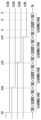
도 8a 내지 도 8b는 도 4에 따른 멀티 플레인 구조를 갖는 메모리 장치의 플레인 인터리브 리드 동작을 나타내는 타이밍도이다.FIGS. 8A and 8B are timing diagrams showing plane interleaved read operations of a memory device having a multi-plane structure according to FIG. 4.
도 8a 및 도 8b를 참조하면, 도 2에 도시된 입출력 패드(DQ)를 통해 수신되는 커맨드(CMD)와 어드레스(ADDR:P1~ADDR:P4), 입출력 패드(DQ)를 통해 출력되는 데이터(DATA OUT:P1~DATA OUT:P4), 도 2의 RB 패드를 통해 출력되는 레디비지 신호(RB:P1~RB:P4)가 도시되어 있다. RB 패드를 통해 출력되는 레디비지 신호(RB:P1~RB:P4)는 메모리 장치(1100)에 포함된 플레인들(P1, P2, P3, P4) 각각의 레디 상태 또는 비지 상태를 나타낼 수 있다.Referring to FIGS. 8A and 8B, a command (CMD) and an address (ADDR:P1 to ADDR:P4) received through the input/output pads (DQ) illustrated in FIG. 2, data (DATA OUT:P1 to DATA OUT:P4) output through the input/output pads (DQ), and a ready-busy signal (RB:P1 to RB:P4) output through the RB pads of FIG. 2 are illustrated. The ready-busy signal (RB:P1 to RB:P4) output through the RB pads can indicate a ready state or a busy state of each of the planes (P1, P2, P3, P4) included in the memory device (1100).
제1 시각(t1)에서, 메모리 장치(1100)는 입출력 패드(DQ)를 통해 제1 페이지 리드 커맨드(00h)를 수신할 수 있다. 제2 시각(t2)에서, 메모리 장치(1100)는 입출력 패드(DQ)를 통해 리드 대상이 되는 제1 플레인(P1)의 페이지에 대응하는 어드레스(ADDR:P1)를 수신할 수 있다. 제3 시각(t3)에서, 메모리 장치(1100)는 입출력 패드(DQ)를 통해 제2 페이지 리드 커맨드(30h)를 수신할 수 있다. 제1 페이지 리드 커맨드(00h), 제1 플레인(P1)의 페이지에 대응하는 어드레스(ADDR:P1) 및 제2 페이지 리드 커맨드(30h)는 제1 플레인(P1)에 대한 리드 커맨드를 구성할 수 있다. 제1 플레인(P1)에 대한 리드 커맨드를 수신함에 따라, 제1 플레인(P1)에 대한 리드 동작이 시작될 수 있다. 이에 따라 제4 시각(t4)에서, 제1 플레인(P1)의 레디비지 신호(RB:P1)가 레디 상태를 나타내는 하이(high)에서 비지 상태를 나타내는 로우(low)로 전환될 수 있다.At a first time point (t1), the memory device (1100) can receive a first page read command (00h) through an input/output pad (DQ). At a second time point (t2), the memory device (1100) can receive an address (ADDR:P1) corresponding to a page of the first plane (P1) to be read through the input/output pad (DQ). At a third time point (t3), the memory device (1100) can receive a second page read command (30h) through the input/output pad (DQ). The first page read command (00h), the address (ADDR:P1) corresponding to the page of the first plane (P1), and the second page read command (30h) can constitute a read command for the first plane (P1). Upon receiving a read command for the first plane (P1), a read operation for the first plane (P1) may be initiated. Accordingly, at a fourth time point (t4), a ready-busy signal (RB:P1) of the first plane (P1) may be switched from high indicating a ready state to low indicating a busy state.
제5 시각(t5) 내지 제6 시각(t6)에서, 메모리 장치(1100)는 입출력 패드(DQ)를 통해 제1 페이지 리드 커맨드(00h), 제2 플레인(P2)의 페이지에 대응하는 어드레스(ADDR:P2), 제2 페이지 리드 커맨드(30h)를 수신할 수 있다. 제1 페이지 리드 커맨드(00h), 제2 플레인(P2)의 페이지에 대응하는 어드레스(ADDR:P2) 및 제2 페이지 리드 커맨드(30h)는 제2 플레인(P2)에 대한 리드 커맨드를 구성할 수 있다. 제2 플레인(P2)에 대한 리드 커맨드를 수신함에 따라, 제2 플레인(P2)에 대한 리드 동작이 시작될 수 있다. 이에 따라 제6 시각(t6)에서, 제2 플레인(P2)의 레디비지 신호(RB:P2)가 레디 상태를 나타내는 하이(high)에서 비지 상태를 나타내는 로우(low)로 전환될 수 있다.At a fifth time point (t5) to a sixth time point (t6), the memory device (1100) can receive a first page read command (00h), an address (ADDR:P2) corresponding to a page of the second plane (P2), and a second page read command (30h) through an input/output pad (DQ). The first page read command (00h), the address (ADDR:P2) corresponding to a page of the second plane (P2), and the second page read command (30h) can constitute a read command for the second plane (P2). Upon receiving the read command for the second plane (P2), a read operation for the second plane (P2) can be started. Accordingly, at the sixth time point (t6), the ready-busy signal (RB:P2) of the second plane (P2) can be switched from high indicating a ready state to low indicating a busy state.
제7 시각(t7) 내지 제8 시각(t8)에서, 메모리 장치(1100)는 입출력 패드(DQ)를 통해 제1 페이지 리드 커맨드(00h), 제3 플레인(P3)의 페이지에 대응하는 어드레스(ADDR:P3), 제2 페이지 리드 커맨드(30h)를 수신할 수 있다. 제1 페이지 리드 커맨드(00h), 제3 플레인(P3)의 페이지에 대응하는 어드레스(ADDR:P3) 및 제2 페이지 리드 커맨드(30h)는 제3 플레인(P3)에 대한 리드 커맨드를 구성할 수 있다. 제3 플레인(P3)에 대한 리드 커맨드를 수신함에 따라, 제3 플레인(P3)에 대한 리드 동작이 시작될 수 있다. 이에 따라 제8 시각(t8)에서, 제3 플레인(P3)의 레디비지 신호(RB:P3)가 레디 상태를 나타내는 하이(high)에서 비지 상태를 나타내는 로우(low)로 전환될 수 있다.At a seventh time (t7) to an eighth time (t8), the memory device (1100) can receive a first page read command (00h), an address (ADDR:P3) corresponding to a page of the third plane (P3), and a second page read command (30h) through an input/output pad (DQ). The first page read command (00h), the address (ADDR:P3) corresponding to a page of the third plane (P3), and the second page read command (30h) can constitute a read command for the third plane (P3). Upon receiving the read command for the third plane (P3), a read operation for the third plane (P3) can be started. Accordingly, at the 8th time point (t8), the ready-busy signal (RB:P3) of the third plane (P3) can be switched from high indicating a ready state to low indicating a busy state.
제9 시각(t9) 내지 제10 시각(t10)에서, 메모리 장치(1100)는 입출력 패드(DQ)를 통해 제1 페이지 리드 커맨드(00h), 제4 플레인(P4)의 페이지에 대응하는 어드레스(ADDR:P4), 제2 페이지 리드 커맨드(30h)를 수신할 수 있다. 제1 페이지 리드 커맨드(00h), 제4 플레인(P4)의 페이지에 대응하는 어드레스(ADDR:P4) 및 제2 페이지 리드 커맨드(30h)는 제4 플레인(P4)에 대한 리드 커맨드를 구성할 수 있다. 제4 플레인(P4)에 대한 리드 커맨드를 수신함에 따라, 제4 플레인(P4)에 대한 리드 동작이 시작될 수 있다. 이에 따라 제10 시각(t10)에서, 제4 플레인(P4)의 레디비지 신호(RB:P4)가 레디 상태를 나타내는 하이(high)에서 비지 상태를 나타내는 로우(low)로 전환될 수 있다.At a ninth time point (t9) to a tenth time point (t10), the memory device (1100) can receive a first page read command (00h), an address (ADDR:P4) corresponding to a page of the fourth plane (P4), and a second page read command (30h) through an input/output pad (DQ). The first page read command (00h), the address (ADDR:P4) corresponding to a page of the fourth plane (P4), and the second page read command (30h) can constitute a read command for the fourth plane (P4). Upon receiving the read command for the fourth plane (P4), a read operation for the fourth plane (P4) can be started. Accordingly, at the 10th time (t10), the ready-busy signal (RB:P4) of the 4th plane (P4) can be switched from high indicating a ready state to low indicating a busy state.
도 8b를 참조하면, 제11 시각(t11)에서, 제1 플레인(P1)에 대한 리드 동작이 완료될 수 있다. 이에 따라, 제11 시각(t11)에서 제1 플레인(P1)의 레디비지 신호(RB:P1)가 로우 값에서 하이 값으로 변경된다. 메모리 장치(1100)는 제11 시각(t11) 내지 제12 시각(t12) 동안 입출력 패드(DQ)를 통해 제1 플레인(P1)에 대한 리드 데이터(DATA OUT:P1)를 출력할 수 있다.Referring to FIG. 8B, at an eleventh time point (t11), a read operation for the first plane (P1) may be completed. Accordingly, at the eleventh time point (t11), a ready-to-use signal (RB:P1) of the first plane (P1) changes from a low value to a high value. The memory device (1100) may output read data (DATA OUT:P1) for the first plane (P1) through the input/output pad (DQ) during the eleventh time point (t11) to the twelfth time point (t12).
제13 시각(t13)에서, 제2 플레인(P2)에 대한 리드 동작이 완료될 수 있다. 이에 따라, 제13 시각(t13)에서 제2 플레인(P2)의 레디비지 신호(RB:P2)가 로우 값에서 하이 값으로 변경된다. 메모리 장치(1100)는 제13 시각(t13) 내지 제14 시각(t14) 동안 입출력 패드(DQ)를 통해 제2 플레인(P2)에 대한 리드 데이터(DATA OUT:P2)를 출력할 수 있다.At the 13th time point (t13), a read operation for the second plane (P2) can be completed. Accordingly, the ready-to-use signal (RB:P2) of the second plane (P2) changes from a low value to a high value at the 13th time point (t13). The memory device (1100) can output read data (DATA OUT:P2) for the second plane (P2) through the input/output pad (DQ) during the 13th time point (t13) to the 14th time point (t14).
제15 시각(t15)에서, 제3 플레인(P3)에 대한 리드 동작이 완료될 수 있다. 이에 따라, 제15 시각(t15)에서 제3 플레인(P3)의 레디비지 신호(RB:P3)가 로우 값에서 하이 값으로 변경된다. 메모리 장치(1100)는 제15 시각(t15) 내지 제16 시각(t16) 동안 입출력 패드(DQ)를 통해 제3 플레인(P3)에 대한 리드 데이터(DATA OUT:P3)를 출력할 수 있다.At the 15th time point (t15), a read operation for the third plane (P3) can be completed. Accordingly, the ready-to-use signal (RB:P3) of the third plane (P3) changes from a low value to a high value at the 15th time point (t15). The memory device (1100) can output read data (DATA OUT:P3) for the third plane (P3) through the input/output pad (DQ) during the 15th time point (t15) to the 16th time point (t16).
제17 시각(t17)에서, 제4 플레인(P4)에 대한 리드 동작이 완료될 수 있다. 이에 따라, 제17 시각(t17)에서 제4 플레인(P4)의 레디비지 신호(RB:P4)가 로우 값에서 하이 값으로 변경된다. 메모리 장치(1100)는 제17 시각(t17)부터 입출력 패드(DQ)를 통해 제4 플레인(P4)에 대한 리드 데이터(DATA OUT:P4)를 출력할 수 있다.At the 17th time point (t17), the read operation for the 4th plane (P4) can be completed. Accordingly, the ready-to-use signal (RB:P4) of the 4th plane (P4) changes from a low value to a high value at the 17th time point (t17). The memory device (1100) can output read data (DATA OUT:P4) for the 4th plane (P4) through the input/output pad (DQ) from the 17th time point (t17).
도 8a 및 도 8b에 도시된 바와 같이, 멀티 플레인 구조를 갖는 메모리 장치(1100)는 어느 하나의 플레인에 대한 리드 동작이 시작되고 리드 동작이 종료되기 전에, 다른 플레인에 대한 리드 커맨드를 수신하고, 상기 다른 플레인에 대한 리드 동작을 시작할 수 있다.As illustrated in FIGS. 8A and 8B, a memory device (1100) having a multi-plane structure can receive a read command for another plane and start a read operation for the other plane before a read operation for one plane is started and ended.
상술한 것처럼, 플레인들 각각의 리드 동작이 병렬적으로 수행되거나 적어도 일부의 시간 구간에서 서로 중첩하여 수행되는 것을 플레인 인터리브 리드 동작으로 지칭할 수 있다. 이처럼, 플레인 인터리브 리드 동작은 복수의 플레인들에 대한 리드 동작이 중첩하여 수행되기 때문에 메모리 장치의 동작 속도가 향상될 수 있다.As described above, the read operations of each plane are performed in parallel or overlapped with each other in at least some time intervals, which may be referred to as a plane interleaved read operation. In this way, the plane interleaved read operation can improve the operating speed of the memory device because the read operations for multiple planes are performed in an overlapped manner.
도 9는 트리플 레벨 셀 형태의 메모리 셀들의 문턱전압 분포를 설명하기 위한 도면이다.Figure 9 is a drawing for explaining the threshold voltage distribution of memory cells in the triple-level cell form.
도 9를 참조하면, 멀티 레벨 셀(multi-level cell; MLC)이 적용되는 메모리 장치(1100)에서 메모리 셀들의 문턱 전압 분포는 4 개 이상일 수 있다. 즉, 메모리 셀들의 상태가 적어도 4 개의 문턱 전압 분포로 구분되는 데이터 저장 방법을 일반적으로 멀티 레벨 셀(MLC)이라 한다. 예를 들면, 메모리 셀들은 소거 상태, 제1 프로그램 상태, 제2 프로그램 상태 또는 제3 프로그램 상태에 따라 다른 데이터를 가질 수 있다. 8 개의 문턱 전압 분포로 메모리 셀들이 구분되는 데이터 저장 방법을 트리플 레벨 셀(TLC)이라고 하고, 16 개의 문턱 전압 분포로 메모리 셀들이 구분되는 데이터 저장 방법을 쿼드러플 레벨 셀(QLC)이라고 한다. 본 실시예는 멀티 레벨 셀(MLC), 트리플 레벨 셀(TLC) 및 쿼드러플 레벨 셀(QLC)에도 적용될 수 있으며, 16개 이상의 문턱 전압 분도로 메모리 셀들이 구분되는 방법에도 적용될 수 있다.Referring to FIG. 9, in a memory device (1100) to which a multi-level cell (MLC) is applied, threshold voltage distributions of memory cells may be four or more. That is, a data storage method in which the states of memory cells are distinguished by at least four threshold voltage distributions is generally referred to as a multi-level cell (MLC). For example, memory cells may have different data depending on an erase state, a first program state, a second program state, or a third program state. A data storage method in which memory cells are distinguished by eight threshold voltage distributions is referred to as a triple-level cell (TLC), and a data storage method in which memory cells are distinguished by 16 threshold voltage distributions is referred to as a quadruple-level cell (QLC). The present embodiment can be applied to a multi-level cell (MLC), a triple-level cell (TLC), and a quadruple-level cell (QLC), and can also be applied to a method in which memory cells are distinguished by 16 or more threshold voltage distributions.
도 9를 참조하면, 트리플 레벨 셀(TLC)의 문턱 전압 분포가 예시적으로 도시된다.Referring to Figure 9, the threshold voltage distribution of a triple-level cell (TLC) is illustrated as an example.
트리플 레벨 셀(TLC)에서 메모리 셀들은 8 개의 문턱 전압 분포를 가질 수 있다. 예를 들면, 메모리 셀들은 문턱 전압 분포에 따라 소거 상태(ER) 및 제1 내지 제7 프로그램 상태들(PV1~PV7)로 구분될 수 있다. 각각의 문턱 전압 분포에 따라 메모리 셀들에는 그레이 코드(gray code)가 부여될 수 있으며, 메모리 셀들은 그레이 코드에 따라 프로그램 될 수 있고, 리드 될 수 있다. 트리플 레벨 셀(TLC)에서는 하나의 메모리 셀이 세 개의 그레이 코드로 구분될 수 있다. 트리플 레셀 셀(TLC)에서 그레이 코드는 하위 비트(LSB), 중앙 비트(CSB) 및 상위 비트(MSB)를 포함할 수 있으며, 메모리 셀들은 그레이 코드의 조합에 따라 8 개의 상태로 구분될 수 있다.In a triple-level cell (TLC), memory cells can have eight threshold voltage distributions. For example, the memory cells can be classified into an erase state (ER) and first to seventh program states (PV1 to PV7) according to the threshold voltage distribution. A gray code can be assigned to the memory cells according to each threshold voltage distribution, and the memory cells can be programmed and read according to the gray code. In a triple-level cell (TLC), one memory cell can be classified into three gray codes. In a triple-level cell (TLC), the gray code can include a lower bit (LSB), a center bit (CSB), and a higher bit (MSB), and the memory cells can be classified into eight states according to a combination of gray codes.
예를 들면, 소거 상태(ER)의 그레이 코드는 ‘111’로 설정될 수 있고, 제1 프로그램 상태(PV1)의 그레이 코드는 ‘110’으로 설정될 수 있고, 제7 프로그램 상태(PV7)의 그레이 코드는 ‘011’로 설정될 수 있다. 그레이 코드의 조합은 메모리 장치(1100)에 따라 다를 수 있으며, 이에 따라 리드 동작에 사용되는 리드 전압 또한 그레이 코드에 따라 달라질 수 있다. 도 9에 도시된 그레이 코드를 예를 들어 설명하면, 하위 비트(LSB) 리드 동작에서는 하나의 LSB 리드 전압(VLSB)이 사용될 수 있고, 중앙 비트(CSB) 리드 동작에서는 두 개의 CSB 리드 전압들(VCSB)이 사용될 수 있으며, 상위 비트(MSB) 리드 동작에서는 네 개의 MSB 리드 전압들(VMSB)이 사용될 수 있다.For example, the gray code of the erase state (ER) may be set to ‘111’, the gray code of the first program state (PV1) may be set to ‘110’, and the gray code of the seventh program state (PV7) may be set to ‘011’. The combination of gray codes may vary depending on the memory device (1100), and accordingly, the read voltage used for the read operation may also vary depending on the gray code. Taking the gray code illustrated in FIG. 9 as an example, one LSB read voltage (VLSB) may be used in a lower bit (LSB) read operation, two CSB read voltages (VCSB) may be used in a center bit (CSB) read operation, and four MSB read voltages (VMSB) may be used in a higher bit (MSB) read operation.
따라서, 하위 비트(LSB), 중앙 비트(CSB) 및 상위 비트(MSB) 각각에 대한 리드 동작이 서로 구분된다. 이하에서는, 특정 페이지에서 하위 비트(LSB)를 리드하는 동작을 LSB 페이지 리드 동작으로 지칭하고, 중앙 비트(CSB)를 리드하는 동작을 CSB 페이지 리드 동작으로 지칭하고, 상위 비트(MSB)를 리드하는 동작을 MSB 페이지 리드 동작으로 지칭한다.Therefore, the read operations for the lower bit (LSB), the center bit (CSB), and the upper bit (MSB) are distinguished from each other. Hereinafter, the operation of reading the lower bit (LSB) in a specific page is referred to as an LSB page read operation, the operation of reading the center bit (CSB) is referred to as a CSB page read operation, and the operation of reading the upper bit (MSB) is referred to as an MSB page read operation.
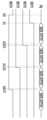
도 10은 도 4에 따른 멀티 플레인 구조를 갖는 메모리 장치에서 플레인 인터리브 리드 동작에 따른 제어 메모리의 활용 방법을 설명하기 위한 개념도이다.FIG. 10 is a conceptual diagram for explaining a method of utilizing control memory according to plane interleaved read operation in a memory device having a multi-plane structure according to FIG. 4.
도 10을 참조하면, 제1 내지 제4 제어 메모리(CM1~CM4) 각각은, 프로그램 동작, 리드 동작, 소거 동작 등을 비롯한 전반적인 동작을 위한 코드를 저장하는 메인 영역(MA) 및 플레인 인터리브 동작을 수행하기 위한 코드를 저장하는 보조 영역(SA)을 포함할 수 있다. 예를 들어, 보조 영역(SA)은, LSB 페이지 리드 동작을 수행하기 위한 LSB 코드(LSBC), CSB 페이지 리드 동작을 수행하기 위한 CSB 코드(CSBC), 및 MSB 페이지 리드 동작을 수행하기 위한 MSB 코드(MSBC)를 포함할 수 있다.Referring to FIG. 10, each of the first to fourth control memories (CM1 to CM4) may include a main area (MA) that stores codes for overall operations including program operations, read operations, and erase operations, and an auxiliary area (SA) that stores codes for performing a plane interleave operation. For example, the auxiliary area (SA) may include an LSB code (LSBC) for performing an LSB page read operation, a CSB code (CSBC) for performing a CSB page read operation, and an MSB code (MSBC) for performing an MSB page read operation.
도 10에서는 제1 내지 제4 제어 메모리(CM1~CM4)가 각각 메인 영역(MA)과 보조 영역(SA)을 포함하는 것으로 도시하였으나, 제1 내지 제4 제어 메모리(CM1~CM4)의 메인 영역(MA)을 하나의 메인 메모리로 구성할 수도 있고, 보조 영역(SA)을 각각의 보조 메모리로 구성할 수도 있다. 이때, 메인 메모리로 구성된 메인 영역(MA)은 플레인 인터리브 동작을 수행하기 위한 코드를 추가로 저장하여 보조 메모리 하나를 대체할 수도 있다. 또한, 제어 로직들(CL1~CL4)이 도 4에 도시된 페이지 버퍼 그룹들(PBG1~PBG4) 각각의 제어를 위한 제어 코드를 다른 제어 코드들과 분리하여 독립적으로 접근할 수 있도록, 메인 메모리와 보조 메모리들 중 적어도 하나는, 페이지 버퍼 그룹을 제어하기 위한 제어 코드를 저장하는 메모리(또는 영역)와 나머지 제어 코드를 저장하는 메모리로 구성될 수도 있다.In FIG. 10, the first to fourth control memories (CM1 to CM4) are illustrated as including a main area (MA) and an auxiliary area (SA), respectively. However, the main areas (MAs) of the first to fourth control memories (CM1 to CM4) may be configured as one main memory, and the auxiliary areas (SAs) may be configured as each auxiliary memory. In this case, the main area (MA) configured as the main memory may additionally store a code for performing a plane interleave operation, thereby replacing one auxiliary memory. In addition, so that the control logics (CL1 to CL4) can independently access the control codes for controlling each of the page buffer groups (PBG1 to PBG4) illustrated in FIG. 4 by separating them from other control codes, at least one of the main memory and the auxiliary memories may be configured as a memory (or area) for storing a control code for controlling a page buffer group and a memory for storing the remaining control codes.
한편, 메모리 컨트롤러(1200)는 메모리 장치(1100)의 제어 로직들(CL1~CL4)에 플레인 인터리브 리드 동작을 지시하는 리드 커맨드를 전송할 수 있다. 예를 들어, 리드 커맨드는, 복수의 플레인들 중에서 선택된 플레인의 LSB 페이지 리드 동작을 지시하는 LSB 리드 커맨드, 상기 선택된 플레인의 CSB 페이지 리드 동작을 지시하는 CSB 리드 커맨드, 상기 선택된 플레인의 MSB 페이지 리드 동작을 지시하는 MSB 리드 커맨드 중 하나일 수 있다.Meanwhile, the memory controller (1200) may transmit a read command that instructs a plane interleaved read operation to the control logics (CL1 to CL4) of the memory device (1100). For example, the read command may be one of an LSB read command that instructs an LSB page read operation of a plane selected from among a plurality of planes, a CSB read command that instructs a CSB page read operation of the selected plane, and an MSB read command that instructs an MSB page read operation of the selected plane.
이하에서는, 플레인 인터리브 리드 동작을 위해 메모리 컨트롤러(1200)는 제1 제어 로직(CL1)에 제1 플레인(P1)에 대한 LSB 리드 커맨드를 전송하고, 제2 제어 로직(CL2)에 제2 플레인(P2)에 대한 CSB 리드 커맨드를 전송하고, 제3 제어 로직(CL3)에 제3 플레인(P3)에 대한 MSB 리드 커맨드를 전송하고, 제4 제어 로직(CL4)에 제4 플레인(P4)에 대한 LSB 리드 커맨드를 전송하는 경우를 설명한다. 그러나 반드시 이에 한정되는 것은 아니며 어떠한 리드 커맨드가 어느 제어 로직에 전송되는지는 호스트(2000)로부터 메모리 컨트롤러(1200)가 수신하는 요청에 따라 결정될 수 있다.Hereinafter, for a plane interleaved read operation, a case will be described in which the memory controller (1200) transmits an LSB read command for the first plane (P1) to the first control logic (CL1), a CSB read command for the second plane (P2) to the second control logic (CL2), an MSB read command for the third plane (P3) to the third control logic (CL3), and an LSB read command for the fourth plane (P4) to the fourth control logic (CL4). However, it is not necessarily limited thereto, and which read command is transmitted to which control logic may be determined according to a request received by the memory controller (1200) from the host (2000).
먼저, 제1 제어 로직(CL1)은, LSB 리드 커맨드에 대한 응답으로, 제1 제어 메모리(CM1)로부터 LSB 코드(LSBC)를 획득하고, 획득된 LSB 코드(LSBC)를 참조하여 제1 플레인(P1)에 대한 LSB 페이지 리드 동작을 제1 시각(TP1)부터 수행할 수 있다.First, the first control logic (CL1) can, in response to the LSB read command, obtain an LSB code (LSBC) from the first control memory (CM1) and perform an LSB page read operation for the first plane (P1) from the first time (TP1) by referring to the obtained LSB code (LSBC).
제2 제어 로직(CL2)은, CSB 리드 커맨드에 대한 응답으로, 제2 제어 메모리(CM2)로부터 CSB 코드(CSBC)를 획득하고, 획득된 CSB 코드(CSBC)를 참조하여 제2 플레인(P2)에 대한 CSB 페이지 리드 동작을 제2 시각(TP2)부터 수행할 수 있다.The second control logic (CL2) can, in response to the CSB read command, obtain a CSB code (CSBC) from the second control memory (CM2) and perform a CSB page read operation for the second plane (P2) from the second time (TP2) by referring to the obtained CSB code (CSBC).
제3 제어 로직(CL3)은, MSB 리드 커맨드에 대한 응답으로, 제3 제어 메모리(CM3)로부터 MSB 코드(MSBC)를 획득하고, 획득된 MSB 코드(MSBC)를 참조하여 제3 플레인(P3)에 대한 MSB 페이지 리드 동작을 제3 시각(TP3)부터 수행할 수 있다.The third control logic (CL3) can, in response to the MSB read command, obtain an MSB code (MSBC) from the third control memory (CM3) and perform an MSB page read operation for the third plane (P3) from the third time (TP3) by referring to the obtained MSB code (MSBC).
제4 제어 로직(CL4)은, LSB 리드 커맨드에 대한 응답으로, 제4 제어 메모리(CM4)로부터 LSB 코드(LSBC)를 획득하고, 획득된 LSB 코드(LSBC)를 참조하여 제4 플레인(P4)에 대한 LSB 페이지 리드 동작을 제4 시각(TP4)부터 수행할 수 있다.The fourth control logic (CL4) can, in response to the LSB read command, obtain an LSB code (LSBC) from the fourth control memory (CM4) and perform an LSB page read operation for the fourth plane (P4) from the fourth time (TP4) by referring to the obtained LSB code (LSBC).
상술한 것처럼, 제어 로직들(CL1~CL4) 각각이 독립한 제어 메모리를 사용하는 경우, 제어 로직들(CL1~CL4) 사이에 제어 메모리를 동시에 접근하지 않기 때문에 각 플레인에 대하여 병렬적으로 리드 동작이 수행될 수 있는 장점이 있다.As described above, when each of the control logics (CL1 to CL4) uses an independent control memory, there is an advantage in that read operations can be performed in parallel for each plane because the control memory is not accessed simultaneously between the control logics (CL1 to CL4).
그러나, 제어 메모리들(CM1~CM4) 각각이 LSB 코드(LSBC), CSB 코드(CSBC), 및 MSB 코드(MSBC)를 별로도 저장하고, 그 중 하나의 코드만을 제어 로직이 사용하게 되므로, 저장 공간의 비효율성을 야기할 수 있다. 특히, 제어 메모리들(CM1~CM4)이 차지하는 저장 공간이 늘어날 경우 주변 회로(200)의 크기가 증가하기 때문에 메모리 장치(1100)에 메모리 셀 어레이(100)가 차지하는 면적이 줄어들게 될 수 있다.However, since each of the control memories (CM1 to CM4) separately stores the LSB code (LSBC), the CSB code (CSBC), and the MSB code (MSBC), and the control logic uses only one of the codes, this may cause inefficiency in storage space. In particular, if the storage space occupied by the control memories (CM1 to CM4) increases, the size of the peripheral circuit (200) increases, and thus the area occupied by the memory cell array (100) in the memory device (1100) may decrease.
따라서, 이하에서는 제어 로직들의 병렬적인 동작을 최대한 보장하면서도 저장 공간을 최소화하여 사용할 수 있는 플레인 인터리브 동작을 설명한다.Therefore, below, we describe a plain interleaved operation that can minimize storage space while ensuring the parallel operation of control logics to the maximum extent possible.
도 11은 도 10에 따른 제어 메모리와 다른 형태로 제어 메모리를 구성하여 플레인 인터리브 리드 동작을 수행하는 방법을 설명하기 위한 개념도이다.FIG. 11 is a conceptual diagram for explaining a method of performing a plain interleaved read operation by configuring a control memory in a different form from the control memory according to FIG. 10.
도 11을 참조하면, 도 10에서와 마찬가지로, 플레인 인터리브 리드 동작을 위해 메모리 컨트롤러(1200)는 제1 제어 로직(CL1)에 제1 플레인(P1)에 대한 LSB 리드 커맨드를 전송하고, 제2 제어 로직(CL2)에 제2 플레인(P2)에 대한 CSB 리드 커맨드를 전송하고, 제3 제어 로직(CL3)에 제3 플레인(P3)에 대한 MSB 리드 커맨드를 전송하고, 제4 제어 로직(CL4)에 제4 플레인(P4)에 대한 LSB 리드 커맨드를 전송하는 경우를 설명한다.Referring to FIG. 11, as in FIG. 10, a case is described where, for a plane interleaved read operation, the memory controller (1200) transmits an LSB read command for the first plane (P1) to the first control logic (CL1), a CSB read command for the second plane (P2) to the second control logic (CL2), an MSB read command for the third plane (P3) to the third control logic (CL3), and an LSB read command for the fourth plane (P4) to the fourth control logic (CL4).
다만, 도 10에서와 달리, 제어 메모리(270)는 제어 로직들(CL1~CL4)이 모두 접근 가능한 공통 저장부(common memory, CMM) 및 임시 저장부(SR)를 포함할 수 있다. 예를 들어, 공통 저장부(CMM)는, 롬(Read Only Memory; ROM), PROM (Programmable ROM), EPROM (Electrically Programmable ROM), EEPROM (Electrically Erasable and Programmable ROM) 등일 수 있다.However, unlike in Fig. 10, the control memory (270) may include a common memory (CMM) and a temporary storage (SR) that are accessible to all control logics (CL1 to CL4). For example, the common storage (CMM) may be a Read Only Memory (ROM), a Programmable ROM (PROM), an Electrically Programmable ROM (EPROM), an Electrically Erasable and Programmable ROM (EEPROM), etc.
공통 저장부(CMM)는, 도 10을 참조하여 설명한 제1 내지 제4 제어 메모리(CM1~CM4)와 마찬가지로, 프로그램 동작, 리드 동작, 소거 동작 등을 비롯한 전반적인 동작을 위한 코드를 저장하는 메인 영역(MA) 및 플레인 인터리브 동작을 수행하기 위한 코드를 저장하는 보조 영역(SA)을 포함할 수 있다.The common storage unit (CMM) may include a main area (MA) that stores codes for overall operations including program operations, read operations, and erase operations, and an auxiliary area (SA) that stores codes for performing plain interleave operations, similar to the first to fourth control memories (CM1 to CM4) described with reference to FIG. 10.
제어 로직들(CL1~CL4)이 임시 저장부(SR)에 동시에 접근할 수 있도록, 임시 저장부(SR)는 플레인들(P1~P4) 각각과 대응하고 물리적으로 독립된 영역들을 포함할 수 있다. 예를 들어, 도 4에 따른 예시와 같이 제1 내지 제4 플레인(P1~P4)이 있는 경우, 임시 저장부(SR)는 제1 내지 제4 영역(AR1~AR4)을 포함할 수 있다. 영역들(AR1~AR4) 각각은 서로 물리적으로 구분되는 쉬프트 레지스터(shift register)일 수 있다. 예를 들어, 영역들(AR1~AR4) 각각은, 새로운 데이터가 입력되면 기 저장된 데이터가 삭제되는 쉬프트 레지스터일 수 있다. 제어 로직들(CL1~CL4)은 영역들(AR1~AR4) 각각에 개별적으로(또는 독립적으로) 접근하여 제어 코드를 획득할 수 있다.In order for the control logics (CL1 to CL4) to be able to access the temporary storage (SR) simultaneously, the temporary storage (SR) may include physically independent areas corresponding to each of the planes (P1 to P4). For example, in the case of the first to fourth planes (P1 to P4) as in the example according to FIG. 4, the temporary storage (SR) may include the first to fourth areas (AR1 to AR4). Each of the areas (AR1 to AR4) may be a shift register that is physically distinct from each other. For example, each of the areas (AR1 to AR4) may be a shift register in which previously stored data is deleted when new data is input. The control logics (CL1 to CL4) may individually (or independently) access each of the areas (AR1 to AR4) to obtain a control code.
먼저, 제1 제어 로직(CL1)은, LSB 리드 커맨드에 대한 응답으로, 수신된 LSB 리드 커맨드와 대응하는 LSB 코드(LSBC)가 임시 저장부(SR)에 저장되어 있는지 판단할 수 있다. 임시 저장부(SR)에 저장되어 있지 않은 것으로 판단되면, 제1 제어 로직(CL1)은, 공통 저장부(CMM)로부터 LSB 코드(LSBC)를 획득하고, 획득된 LSB 코드(LSBC)를 임시 저장부(SR)의 제1 영역(AR1)에 저장할 수 있다. 다음으로, 제1 제어 로직(CL1)은, 공통 저장부(CMM)에 저장된 LSB 코드(LSBC)를 참조하여 제1 플레인(P1)에 대한 LSB 페이지 리드 동작을 제1 시각(TP1)부터 수행할 수 있다.First, the first control logic (CL1) can determine, in response to the LSB read command, whether the LSB code (LSBC) corresponding to the received LSB read command is stored in the temporary storage (SR). If it is determined that the LSB code (LSBC) is not stored in the temporary storage (SR), the first control logic (CL1) can obtain the LSB code (LSBC) from the common storage (CMM) and store the obtained LSB code (LSBC) in the first area (AR1) of the temporary storage (SR). Next, the first control logic (CL1) can perform an LSB page read operation for the first plane (P1) from the first time (TP1) by referring to the LSB code (LSBC) stored in the common storage (CMM).
제2 제어 로직(CL2)은, CSB 리드 커맨드에 대한 응답으로, 수신된 CSB 리드 커맨드가 와 대응하는 CSB 코드(CSBC)가 임시 저장부(SR)에 저장되어 있는지 판단할 수 있다. 임시 저장부(SR)에 저장되어 있지 않은 것으로 판단되면, 제2 제어 로직(CL2)은 공통 저장부(CMM)로부터 CSB 코드(CSBC)를 획득하고, 획득된 CSB 코드(CSBC)를 임시 저장부(SR)의 제2 영역(AR2)에 저장할 수 있다. 다음으로, 제2 제어 로직(CL2)은, 공통 저장부(CMM)에 저장된 CSB 코드(CSBC)를 참조하여 제2 플레인(P2)에 대한 CSB 페이지 리드 동작을 제2 시각(TP2)부터 수행할 수 있다.The second control logic (CL2) can determine, in response to the CSB read command, whether the CSB code (CSBC) corresponding to the received CSB read command is stored in the temporary storage (SR). If it is determined that the CSB code (CSBC) is not stored in the temporary storage (SR), the second control logic (CL2) can obtain the CSB code (CSBC) from the common storage (CMM) and store the obtained CSB code (CSBC) in the second area (AR2) of the temporary storage (SR). Next, the second control logic (CL2) can perform a CSB page read operation for the second plane (P2) from the second time (TP2) by referring to the CSB code (CSBC) stored in the common storage (CMM).
제3 제어 로직(CL3)은, MSB 리드 커맨드에 대한 응답으로, MSB 리드 커맨드와 대응하는 MSB 코드(MSBC)가 임시 저장부(SR)에 저장되어 있는지 판단할 수 있다. 임시 저장부(SR)에 저장되어 있지 않은 것으로 판단되면, 공통 저장부(CMM)로부터 MSB 코드(MSBC)를 획득하고, MSB 코드(MSBC)를 임시 저장부(SR)의 제3 영역(AR3)에 저장할 수 있다. 다음으로, 제3 제어 로직(CL3)은, 공통 저장부(CMM)에 저장된 MSB 코드(MSBC)를 참조하여 제3 플레인(P3)에 대한 MSB 페이지 리드 동작을 제3 시각(TP3)부터 수행할 수 있다.The third control logic (CL3) can determine, in response to the MSB read command, whether the MSB code (MSBC) corresponding to the MSB read command is stored in the temporary storage (SR). If it is determined that the MSB code (MSBC) is not stored in the temporary storage (SR), the third control logic (CL3) can obtain the MSB code (MSBC) from the common storage (CMM) and store the MSB code (MSBC) in the third area (AR3) of the temporary storage (SR). Next, the third control logic (CL3) can perform an MSB page read operation for the third plane (P3) from the third time (TP3) by referring to the MSB code (MSBC) stored in the common storage (CMM).
한편, 제4 제어 로직(CL4)은, LSB 리드 커맨드에 대한 응답으로, 수신된 LSB 리드 커맨드와 대응하는 LSB 코드(LSBC)가 임시 저장부(SR)에 저장되어 있는지 판단할 수 있다. 제1 제어 로직(CL1)에 의해 임시 저장부(SR)의 제1 영역(AR1)에 LSB 코드(LSBC)가 저장되어 있기 때문에, 제4 제어 로직(CL4)은 임시 저장부(SR)에 저장되어 있는 것으로 판단할 수 있다. 제4 제어 로직(CL4)은, 임시 저장부(SR)에 접근하고 임시 저장부(SR)의 제1 영역(AR1)로부터 LSB 코드(LSBC)를 획득하고, 획득된 LSB 코드(LSBC)를 임시 저장부(SR)의 제4 영역(AR4)에 저장할 수 있다. 다음으로, 제4 제어 로직(CL4)은, LSB 코드(LSBC)를 참조하여 제4 플레인(P4)에 대한 LSB 페이지 리드 동작을 제4 시각(TP4)부터 수행할 수 있다.Meanwhile, the fourth control logic (CL4) can determine, in response to the LSB read command, whether the LSB code (LSBC) corresponding to the received LSB read command is stored in the temporary storage (SR). Since the LSB code (LSBC) is stored in the first area (AR1) of the temporary storage (SR) by the first control logic (CL1), the fourth control logic (CL4) can determine that it is stored in the temporary storage (SR). The fourth control logic (CL4) can access the temporary storage (SR), obtain the LSB code (LSBC) from the first area (AR1) of the temporary storage (SR), and store the obtained LSB code (LSBC) in the fourth area (AR4) of the temporary storage (SR). Next, the fourth control logic (CL4) can perform an LSB page read operation for the fourth plane (P4) from the fourth time (TP4) with reference to the LSB code (LSBC).
따라서, 도 11과 같은 제어 메모리(270) 구성에서도 도 10에서와 마찬가지로 다수의 플레인들(예를들어, 제1 플레인(P1) 내지 제4 플레인(P4))에 대하여 서로 중첩된 시간 간격(overlap time) 동안 동시에 리드 커맨드에 따른 페이지 리드 동작이 수행될 수 있다.Accordingly, in a control memory (270) configuration such as that in FIG. 11, page read operations according to read commands can be performed simultaneously for a plurality of planes (e.g., the first plane (P1) to the fourth plane (P4)) during overlapping time intervals, as in FIG. 10.
도 12는 도 11에 따른 제어 메모리 구성에서, 다른 커맨드를 수신하였을 때의 플레인 인터리브 리드 동작을 수행하는 방법을 설명하기 위한 개념도이다.FIG. 12 is a conceptual diagram for explaining a method of performing a plain interleaved read operation when another command is received in the control memory configuration according to FIG. 11.
도 12를 참조하면, 도 11에서의 제어 메모리와 동일한 구성을 가질 수 있다. 다만, 도 11에서와 달리, 도 12에서는, 플레인 인터리브 리드 동작을 위해 메모리 컨트롤러(1200)는 제1 제어 로직(CL1)에 제1 플레인(P1)에 대한 LSB 리드 커맨드를 전송하고, 제2 제어 로직(CL2)에 제2 플레인(P2)에 대한 LSB 리드 커맨드를 전송하고, 제3 제어 로직(CL3)에 제3 플레인(P3)에 대한 LSB 리드 커맨드를 전송하고, 제4 제어 로직(CL4)에 제4 플레인(P4)에 대한 LSB 리드 커맨드를 전송하는 경우를 설명한다.Referring to FIG. 12, it may have the same configuration as the control memory in FIG. 11. However, unlike FIG. 11, FIG. 12 describes a case in which, for a plane interleaved read operation, the memory controller (1200) transmits an LSB read command for the first plane (P1) to the first control logic (CL1), transmits an LSB read command for the second plane (P2) to the second control logic (CL2), transmits an LSB read command for the third plane (P3) to the third control logic (CL3), and transmits an LSB read command for the fourth plane (P4) to the fourth control logic (CL4).
먼저, 제1 제어 로직(CL1)은, LSB 리드 커맨드에 대한 응답으로, 수신된 LSB 리드 커맨드와 대응하는 LSB 코드(LSBC)가 임시 저장부(SR)에 저장되어 있는지 판단할 수 있다. 임시 저장부(SR)에 저장되어 있지 않은 것으로 판단되면, 제1 제어 로직(CL1)은, 공통 저장부(CMM)로부터 LSB 코드(LSBC)를 획득하고, 획득된 LSB 코드(LSBC)를 임시 저장부(SR)의 제1 영역(AR1)에 저장할 수 있다. 다음으로, 제1 제어 로직(CL1)은, 공통 저장부(CMM)에 저장된 LSB 코드(LSBC)를 참조하여 제1 플레인(P1)에 대한 LSB 페이지 리드 동작을 제1 시각(TP1)부터 수행할 수 있다.First, the first control logic (CL1) can determine, in response to the LSB read command, whether the LSB code (LSBC) corresponding to the received LSB read command is stored in the temporary storage (SR). If it is determined that the LSB code (LSBC) is not stored in the temporary storage (SR), the first control logic (CL1) can obtain the LSB code (LSBC) from the common storage (CMM) and store the obtained LSB code (LSBC) in the first area (AR1) of the temporary storage (SR). Next, the first control logic (CL1) can perform an LSB page read operation for the first plane (P1) from the first time (TP1) by referring to the LSB code (LSBC) stored in the common storage (CMM).
제2 제어 로직(CL2)은, LSB 리드 커맨드에 대한 응답으로, 수신된 LSB 리드 커맨드와 대응하는 LSB 코드(LSBC)가 임시 저장부(SR)에 저장되어 있는지 판단할 수 있다. 제1 제어 로직(CL1)에 의해 임시 저장부(SR)의 제1 영역(AR1)에 LSB 코드(LSBC)가 저장되어 있기 때문에, 제2 제어 로직(CL2)은 임시 저장부(SR)에 저장되어 있는 것으로 판단할 수 있다. 이 경우, 제2 제어 로직(CL2)은, 임시 저장부(SR)에 접근하고 임시 저장부(SR)의 제1 영역(AR1)로부터 LSB 코드(LSBC)를 획득하고, 획득된 LSB 코드(LSBC)를 임시 저장부(SR)의 제2 영역(AR2)에 저장할 수 있다. 다음으로, 제2 제어 로직(CL2)은, 제1 영역(AR1)에 저장된 LSB 코드(LSBC)를 참조하여 제2 플레인(P2)에 대한 LSB 페이지 리드 동작을 제2 시각(TP2)부터 수행할 수 있다.The second control logic (CL2) can determine, in response to the LSB read command, whether the LSB code (LSBC) corresponding to the received LSB read command is stored in the temporary storage (SR). Since the LSB code (LSBC) is stored in the first area (AR1) of the temporary storage (SR) by the first control logic (CL1), the second control logic (CL2) can determine that it is stored in the temporary storage (SR). In this case, the second control logic (CL2) can access the temporary storage (SR), obtain the LSB code (LSBC) from the first area (AR1) of the temporary storage (SR), and store the obtained LSB code (LSBC) in the second area (AR2) of the temporary storage (SR). Next, the second control logic (CL2) can perform an LSB page read operation for the second plane (P2) from the second time (TP2) by referring to the LSB code (LSBC) stored in the first area (AR1).
제3 제어 로직(CL3)은, LSB 리드 커맨드에 대한 응답으로, 수신된 LSB 리드 커맨드와 대응하는 LSB 코드(LSBC)가 임시 저장부(SR)에 저장되어 있는지 판단할 수 있다. 제2 제어 로직(CL2)에 의해 임시 저장부(SR)의 제2 영역(AR2)에 LSB 코드(LSBC)가 저장되어 있기 때문에, 제3 제어 로직(CL3)은 임시 저장부(SR)에 LSB 코드(LSBC)가 저장되어 있는 것으로 판단할 수 있다. 이때, 제2 제어 로직(CL2)이 임시 저장부(SR)의 제1 영역(AR1)에 접근하여 LSB 페이지 리드 동작을 수행하고 있기 때문에, 제3 제어 로직(CL3)은 제1 영역(AR1)에 접근할 수 없다. 이 경우, 제3 제어 로직(CL3)은, 임시 저장부(SR)의 제2 영역(AR2)로부터 LSB 코드(LSBC)를 획득하고, 획득된 LSB 코드(LSBC)를 임시 저장부(SR)의 제3 영역(AR3)에 저장할 수 있다. 다음으로, 제3 제어 로직(CL3)은, 제2 영역(AR2)에 저장된 LSB 코드(LSBC)를 참조하여 제3 플레인(P3)에 대한 LSB 페이지 리드 동작을 제3 시각(TP3)부터 수행할 수 있다.The third control logic (CL3) can determine, in response to the LSB read command, whether the LSB code (LSBC) corresponding to the received LSB read command is stored in the temporary storage (SR). Since the LSB code (LSBC) is stored in the second area (AR2) of the temporary storage (SR) by the second control logic (CL2), the third control logic (CL3) can determine that the LSB code (LSBC) is stored in the temporary storage (SR). At this time, since the second control logic (CL2) accesses the first area (AR1) of the temporary storage (SR) to perform the LSB page read operation, the third control logic (CL3) cannot access the first area (AR1). In this case, the third control logic (CL3) can obtain the LSB code (LSBC) from the second area (AR2) of the temporary storage (SR) and store the obtained LSB code (LSBC) in the third area (AR3) of the temporary storage (SR). Next, the third control logic (CL3) can perform an LSB page read operation for the third plane (P3) from the third time (TP3) by referring to the LSB code (LSBC) stored in the second area (AR2).
제4 제어 로직(CL4)은, LSB 리드 커맨드에 대한 응답으로, 수신된 LSB 리드 커맨드와 대응하는 LSB 코드(LSBC)가 임시 저장부(SR)에 저장되어 있는지 판단할 수 있다. 제3 제어 로직(CL3)에 의해 임시 저장부(SR)의 제3 영역(AR3)에 LSB 코드(LSBC)가 저장되어 있기 때문에, 제4 제어 로직(CL4)은 임시 저장부(SR)에 저장되어 있는 것으로 판단할 수 있다. 이때, 제2 제어 로직(CL2)이 임시 저장부(SR)의 제1 영역(AR1)에 접근하여 LSB 페이지 리드 동작을 수행하고 있고, 제3 제어 로직(CL3)이 임시 저장부(SR)의 제2 영역(AR2)에 접근하여 LSB 페이지 리드 동작을 수행하고 있어, 제4 제어 로직(CL4)은, 제1 영역(AR1)과 제2 영역(AR2)에 접근할 수 없다. 이 경우, 제4 제어 로직(CL4)은, 임시 저장부(SR)의 제3 영역(AR3)로부터 LSB 코드(LSBC)를 획득하고, 획득된 LSB 코드(LSBC)를 임시 저장부(SR)의 제4 영역(AR4)에 저장할 수 있다. 다음으로, 제4 제어 로직(CL4)은, 제3 영역(AR3)에 저장된 LSB 코드(LSBC)를 참조하여 제4 플레인(P4)에 대한 LSB 페이지 리드 동작을 제4 시각(TP4)부터 수행할 수 있다.The fourth control logic (CL4) can determine, in response to the LSB read command, whether the LSB code (LSBC) corresponding to the received LSB read command is stored in the temporary storage (SR). Since the LSB code (LSBC) is stored in the third area (AR3) of the temporary storage (SR) by the third control logic (CL3), the fourth control logic (CL4) can determine that it is stored in the temporary storage (SR). At this time, the second control logic (CL2) is accessing the first area (AR1) of the temporary storage (SR) to perform the LSB page read operation, and the third control logic (CL3) is accessing the second area (AR2) of the temporary storage (SR) to perform the LSB page read operation, so the fourth control logic (CL4) cannot access the first area (AR1) and the second area (AR2). In this case, the fourth control logic (CL4) can obtain the LSB code (LSBC) from the third area (AR3) of the temporary storage (SR) and store the obtained LSB code (LSBC) in the fourth area (AR4) of the temporary storage (SR). Next, the fourth control logic (CL4) can perform an LSB page read operation for the fourth plane (P4) from the fourth time (TP4) by referring to the LSB code (LSBC) stored in the third area (AR3).
도 11과 도 12에 따른 설명을 종합하면, 제어 로직들(CL1~CL4)은 메모리 컨트롤러로부터 수신된 리드 커맨드와 대응하는 제어 코드가 임시 저장부(SR)에 없는 경우, 공통 저장부(CMM)로부터 리드 커맨드와 대응하는 제어 코드(LSB 코드, CSB 코드, MSB 코드 중 하나)를 획득할 수 있다. 또한, 리드 커맨드와 대응하는 제어 코드가 임시 저장부(SR)에 있는 경우 임시 저장부(SR)로부터 제어 코드를 획득할 수 있다. 이때, 공통 저장부(CMM) 또는 임시 저장부(SR)에서 획득된 제어 코드를 다른 제어 로직이 참조할 수 있도록, 상기 획득된 제어 코드가 임시 저장부(SR)의 영역들(AR1~AR4) 중 하나에 저장될 수 있다. 이후에, 동일한 리드 커맨드를 다른 제어 로직이 수신하는 경우, 임시 저장부(SR)에 저장된 제어 코드를 참조하여 플레인들 중 하나에 대한 동작을 제어할 수 있다.To summarize the explanation according to FIGS. 11 and 12, the control logics (CL1 to CL4) can obtain a control code (one of an LSB code, a CSB code, and an MSB code) corresponding to the read command from the common storage (CMM) when a control code corresponding to a read command received from a memory controller is not present in the temporary storage (SR). In addition, when a control code corresponding to the read command is present in the temporary storage (SR), the control code can be obtained from the temporary storage (SR). At this time, the obtained control code can be stored in one of the areas (AR1 to AR4) of the temporary storage (SR) so that other control logic can refer to the control code obtained from the common storage (CMM) or the temporary storage (SR). Thereafter, when another control logic receives the same read command, the control code stored in the temporary storage (SR) can be referenced to control an operation for one of the planes.
따라서, 일정한 시간 간격으로 여러 제어 로직들이 동시에(또는 인터리브하게) 리드 동작을 수행하더라도, 리드 동작을 먼저 진행중인 제어 로직이 임시 저장부(SR)에 저장한 제어 코드를 동일한 리드 동작을 수행하는 다른 제어 로직이 획득할 수 있게 되므로, 플레인 인터리브 리드 동작이 원활하게 수행됨과 동시에 저장 공간의 사용을 최소화할 수 있다.Accordingly, even if multiple control logics perform read operations simultaneously (or interleavedly) at regular time intervals, the control code stored in the temporary storage (SR) by the control logic that is performing the read operation first can be acquired by other control logics performing the same read operation, so that the plain interleaved read operation can be performed smoothly while minimizing the use of storage space.
도 13은 도 10 내지 도 11에 따른 제어 메모리 구성을 갖는 메모리 장치의 동작 방법을 나타낸 예시 흐름도이다. 도 14는 도 13에 따른 단계 S110을 일부 구체화한 예시 흐름도이다.Fig. 13 is an exemplary flowchart illustrating an operating method of a memory device having a control memory configuration according to Figs. 10 and 11. Fig. 14 is an exemplary flowchart partially specifying step S110 according to Fig. 13.
도 13을 참조하면, 복수의 플레인들(planes)을 포함하는 메모리 장치의 동작 방법은, 메모리 컨트롤러로부터 상기 플레인들 중 하나에 대한 동작을 지시하는 커맨드를 수신하는 단계(S100); 제어 로직들이 공통적으로 접근 가능한 공통 저장부와 임시 저장부 중 하나에 접근하여 상기 커맨드에 대응하는 제어 코드를 획득하는 단계(S110); 및 상기 제어 코드를 참조하여 상기 커맨드에 대응하는 제어 신호를 생성하는 단계(S120)를 포함할 수 있다.Referring to FIG. 13, a method of operating a memory device including a plurality of planes may include a step of receiving a command from a memory controller for instructing an operation for one of the planes (S100); a step of accessing one of a common storage unit and a temporary storage unit commonly accessible by control logics to obtain a control code corresponding to the command (S110); and a step of generating a control signal corresponding to the command by referencing the control code (S120).
도 14를 참조하면, 상기 제어 코드를 획득하는 단계(S110)는, 상기 커맨드에 대응하는 상기 제어 코드가 임시 저장부에 있는지 판단하고(S111), 상기 임시 저장부에 없으면 공통 저장부에 접근하여 상기 제어 코드를 획득하는 단계(S112)를 포함할 수 있다.Referring to FIG. 14, the step of obtaining the control code (S110) may include the step of determining whether the control code corresponding to the command is in the temporary storage (S111), and if not in the temporary storage, accessing the common storage to obtain the control code (S112).
상기 제어 코드를 획득하는 단계(S110)는, 상기 커맨드에 대응하는 상기 제어 코드가 상기 임시 저장부에 있는지 판단하고(S111), 임시 저장부에 있으면 임시 저장부에 접근하여 상기 제어 코드를 획득하는 단계(S113)를 포함할 수 있다.The step (S110) of obtaining the control code may include a step (S111) of determining whether the control code corresponding to the command is in the temporary storage, and if so, a step (S113) of accessing the temporary storage to obtain the control code.
상기 제어 코드를 획득하는 단계(S110) 이후에, 상기 획득한 제어 코드를 상기 임시 저장부에 저장하는 단계(S114)를 더 포함할 수 있다.After the step (S110) of obtaining the above control code, a step (S114) of storing the obtained control code in the temporary storage unit may be further included.
상기 임시 저장부는, 상기 플레인들 각각에 대응하는 영역들을 포함할 수 있다.The above temporary storage unit may include areas corresponding to each of the planes.
상기 영역들 각각은, 쉬프트 레지스터(shift register)일 수 있다.Each of the above areas may be a shift register.
상기 임시 저장부에 저장하는 단계(S114)는, 상기 영역들 중 상기 제어 코드가 획득된 영역을 제외한 다른 영역에 상기 제어 코드를 저장하는 단계를 포함할 수 있다.The step (S114) of storing in the temporary storage may include a step of storing the control code in an area other than the area from which the control code was obtained among the areas.
상기 커맨드는, LSB 리드 커맨드, CSB 리드 커맨드, MSB 리드 커맨드 중 적어도 하나를 포함할 수 있다.The above command may include at least one of an LSB read command, a CSB read command, and an MSB read command.
상기 제어 코드는, 상기 LSB 리드 커맨드에 따른 LSB 페이지 리드 동작을 수행하기 위한 제어 코드, CSB 리드 커맨드에 따른 CSB 페이지 리드 동작을 수행하기 위한 제어 코드, MSB 리드 커맨드에 따른 MSB 페이지 리드 동작을 수행하기 위한 제어 코드 중 적어도 하나를 포함할 수 있다.The above control code may include at least one of a control code for performing an LSB page read operation according to the LSB read command, a control code for performing a CSB page read operation according to the CSB read command, and a control code for performing an MSB page read operation according to the MSB read command.
상기 플레인들 중 제1 플레인에 대한 동작이 종료되기 전에, 상기 영역들 중 제1 영역에 저장된 제어 코드를 참조하여, 상기 플레인들 중 제2 플레인에 대하여 상기 커맨드와 대응하는 동작을 수행하는 단계를 더 포함할 수 있다.The method may further include a step of performing an operation corresponding to the command for a second plane among the planes by referencing a control code stored in a first area among the areas before the operation for the first plane among the planes is terminated.
상기 제1 영역에 저장된 상기 제어 코드는, 상기 제1 플레인에 대하여 상기 제2 플레인에대한 동작과 동일한 동작을 수행하기 위한 제어 코드일 수 있다.The control code stored in the first region may be a control code for performing the same operation for the first plane as for the second plane.
상기 제1 영역에 저장된 제어 코드는, 상기 영역들 중 제2 영역에 저장될 수 있다.The control code stored in the first area can be stored in the second area among the areas.
상술한 과정들 이외에도, 메모리 장치의 동작 방법은 도 1 내지 도 12에서 설명한 메모리 장치의 구성 및 동작 방법이 적용될 수 있는 것으로 해석되어야 한다.In addition to the processes described above, it should be interpreted that the operating method of the memory device can be applied to the configuration and operating method of the memory device described in FIGS. 1 to 12.
도 15는 도 1의 메모리 컨트롤러를 구체적으로 설명하기 위한 도면이다.Figure 15 is a drawing specifically explaining the memory controller of Figure 1.
도 15를 참조하면, 메모리 컨트롤러(1200)는 내부 메모리(Internal Memory; 1210), 중앙 처리 장치(Central Processing Unit; CPU; 1220), 에러 정정 블록(Error Correction Block; 1230), 호스트 인터페이스(Host Interface; 1240), 버퍼 메모리 인터페이스(Buffer Memory Interface; 1250) 및 메모리 인터페이스(Memory Interface; 1260)를 포함할 수 있다.Referring to FIG. 15, a memory controller (1200) may include an internal memory (1210), a central processing unit (CPU) 1220, an error correction block (1230), a host interface (1240), a buffer memory interface (1250), and a memory interface (1260).
내부 메모리(1210)는 메모리 컨트롤러(1200)의 동작에 필요한 다양한 정보들을 저장할 수 있다. 예를 들면, 내부 메모리(1210)는 논리적, 물리적(logical, physical) 어드레스 맵 테이블들(address map tables)을 포함할 수 있다. 내부 메모리(1210)는 RAM(random access memory), DRAM(dynamic RAM), SRAM(static RAM), 캐시(cache) 및 강하게 결합된 메모리(tightly coupled memory; TCM) 중 적어도 하나 이상으로 구성될 수 있다.The internal memory (1210) can store various information required for the operation of the memory controller (1200). For example, the internal memory (1210) can include logical and physical address map tables. The internal memory (1210) can be configured with at least one of a random access memory (RAM), a dynamic RAM (DRAM), a static RAM (SRAM), a cache, and a tightly coupled memory (TCM).
중앙 처리 장치(1220)는 메모리 장치(1100)를 제어하기 위한 각종 연산을 수행하거나, 다양한 커맨드들(commands)을 생성할 수 있다. 중앙 처리 장치(1220)는 호스트(도 1의 2000)로부터 요청(request)을 수신하면, 수신된 요청에 따라 커맨드를 생성하고, 생성된 커맨드를 메모리 장치(1100)로 전송할 수 있다.The central processing unit (1220) can perform various operations to control the memory device (1100) or generate various commands. When the central processing unit (1220) receives a request from the host (2000 of FIG. 1), it can generate a command according to the received request and transmit the generated command to the memory device (1100).
에러 정정 블록(1230)은 에러 정정 코드(ECC, Error Correcting Code)를 이용하여 메모리 장치(1100)로부터 수신된 데이터의 에러를 검출하고, 정정하도록 구성된다. 중앙 처리 장치(1220)는 에러 정정 블록(1230)의 에러 검출 결과에 따라 읽기 전압을 조절하고, 재 읽기를 수행하도록 메모리 장치(1100)를 제어할 수 있다. 예시적인 실시 예로서, 에러 정정 블록은 메모리 컨트롤러(1200)의 구성 요소로서 제공될 수 있다.The error correction block (1230) is configured to detect and correct errors in data received from the memory device (1100) using an error correction code (ECC). The central processing unit (1220) may control the memory device (1100) to adjust a read voltage and perform a re-read according to the error detection result of the error correction block (1230). As an exemplary embodiment, the error correction block may be provided as a component of the memory controller (1200).
호스트 인터페이스(1240)는 메모리 컨트롤러(1200)와 호스트(도 1의 2000) 사이에서 커맨드, 어드레스 및 데이터 등을 주고받을 수 있다. 예를 들면, 호스트 인터페이스(1240)는 호스트(도 1의 2000)로부터 요청(request), 어드레스 및 데이터 등을 수신할 수 있고, 메모리 장치(1100)로부터 리드된 데이터를 호스트(도 1의 2000)로 출력할 수 있다. 호스트 인터페이스(1240)는 PCIe(Peripheral Component Interconnect Express), ATA(Advanced Technology Attachment), SATA(Serial ATA), PATA(Parallel ATA), SAS(serial attached SCSI) 또는 NVMe(Non-Volatile Memory Express)와 같은 프로토콜을 사용하여 호스트(도 1의 2000)와 통신할 수 있다. 호스트 인터페이스(1240)는 상술한 예에 한정되지 않으며, USB(Universal Serial Bus), MMC(Multi-Media Card), ESDI(Enhanced Small Disk Interface), 또는 IDE(Integrated Drive Electronics) 등과 같은 다양한 인터페이스들을 포함할 수 있다.The host interface (1240) can exchange commands, addresses, and data, etc. between the memory controller (1200) and the host (2000 of FIG. 1). For example, the host interface (1240) can receive requests, addresses, and data, etc. from the host (2000 of FIG. 1), and output data read from the memory device (1100) to the host (2000 of FIG. 1). The host interface (1240) can communicate with the host (2000 of FIG. 1) using a protocol such as Peripheral Component Interconnect Express (PCIe), Advanced Technology Attachment (ATA), Serial ATA (SATA), Parallel ATA (PATA), serial attached SCSI (SAS), or Non-Volatile Memory Express (NVMe). The host interface (1240) is not limited to the examples described above and may include various interfaces such as Universal Serial Bus (USB), Multi-Media Card (MMC), Enhanced Small Disk Interface (ESDI), or Integrated Drive Electronics (IDE).
버퍼 메모리 인터페이스(1250)는 중앙 처리 장치(1220)와 버퍼 메모리(도 1의 1300) 사이에서 데이터를 전송할 수 있다. 버퍼 메모리(도 1의 1300)가 메모리 컨트롤러(1200) 내부에 포함되는 경우에는 버퍼 메모리 인터페이스(1250)는 생략될 수 있다.The buffer memory interface (1250) can transmit data between the central processing unit (1220) and the buffer memory (1300 of FIG. 1). If the buffer memory (1300 of FIG. 1) is included within the memory controller (1200), the buffer memory interface (1250) can be omitted.
메모리 인터페이스(1260)는 메모리 컨트롤러(1200)와 메모리 장치(1100) 사이에서 커맨드, 어드레스 및 데이터 등을 주고받을 수 있다. 예를 들면, 메모리 인터페이스(1260)는 채널(channel)을 통해 메모리 장치(1100)에 커맨드, 어드레스 및 데이터 등을 전송할 수 있고, 메모리 장치(1100)로부터 데이터 등을 수신할 수 있다.The memory interface (1260) can exchange commands, addresses, data, etc. between the memory controller (1200) and the memory device (1100). For example, the memory interface (1260) can transmit commands, addresses, data, etc. to the memory device (1100) through a channel, and can receive data, etc. from the memory device (1100).
도 16은 도 10 내지 도 11에 따른 제어 메모리 구성을 갖는 메모리 장치를 포함하는 메모리 시스템의 다른 실시 예를 설명하기 위한 도면이다.FIG. 16 is a drawing for explaining another embodiment of a memory system including a memory device having a control memory configuration according to FIGS. 10 and 11.
도 16을 참조하면, 메모리 시스템(Memory System)은 호스트(2000) 및 메모리 카드(Memory Card; 70000)를 포함할 수 있다.Referring to FIG. 16, the memory system may include a host (2000) and a memory card (Memory Card; 70000).
메모리 카드(70000)는 스마트 카드(smart card)로 구현될 수 있다. 메모리 카드(70000)는 메모리 장치(1100), 메모리 컨트롤러(1200) 및 카드 인터페이스(Card Interface; 7100)를 포함할 수 있다.The memory card (70000) may be implemented as a smart card. The memory card (70000) may include a memory device (1100), a memory controller (1200), and a card interface (7100).
메모리 컨트롤러(1200)는 메모리 장치(1100)와 카드 인터페이스(7100) 사이에서 데이터의 교환을 제어할 수 있다. 실시 예에 따라, 카드 인터페이스(7100)는 SD(secure digital) 카드 인터페이스 또는 MMC(multi-media card) 인터페이스일 수 있으나 이에 한정되는 것은 아니다. 또한, 카드 인터페이스(7100)는 호스트(HOST; 2000)의 프로토콜에 따라 호스트(2000)와 메모리 컨트롤러(1200) 사이에서 데이터 교환을 인터페이스 할 수 있다. 실시 예에 따라 카드 인터페이스(7100)는 USB(Universal Serial Bus) 프로토콜, IC(InterChip)-USB 프로토콜을 지원할 수 있다. 여기서, 카드 인터페이스(7100)는 호스트(2000)가 사용하는 프로토콜을 지원할 수 있는 하드웨어, 상기 하드웨어에 탑재된 소프트웨어 또는 신호 전송 방법을 의미할 수 있다.The memory controller (1200) can control the exchange of data between the memory device (1100) and the card interface (7100). According to an embodiment, the card interface (7100) can be, but is not limited to, an SD (secure digital) card interface or an MMC (multi-media card) interface. In addition, the card interface (7100) can interface the exchange of data between the host (2000) and the memory controller (1200) according to the protocol of the host (HOST; 2000). According to an embodiment, the card interface (7100) can support a USB (Universal Serial Bus) protocol or an IC (InterChip)-USB protocol. Here, the card interface (7100) can mean hardware capable of supporting a protocol used by the host (2000), software mounted on the hardware, or a signal transmission method.
100: 메모리 셀 어레이200: 주변 회로
210: 전압 생성 회로220: 로우 디코더
230: 페이지 버퍼 그룹240: 컬럼 디코더
250: 입출력 회로260: 전류 센싱 회로
270: 제어 메모리1000: 메모리 시스템
1100: 메모리 장치1200: 메모리 컨트롤러
1210: 내부 메모리1220: 중앙 처리 장치
1230: 에러 정정 블록1240: 호스트 인터페이스
1250: 버퍼 메모리 인터페이스1260: 메모리 인터페이스
1300: 버퍼 메모리2000: 호스트100: Memory cell array 200: Peripheral circuit
210: Voltage generation circuit 220: Row decoder
230: Page Buffer Group 240: Column Decoder
250: Input/output circuit 260: Current sensing circuit
270: Control memory 1000: Memory system
1100: Memory device 1200: Memory controller
1210: Internal memory 1220: Central processing unit
1230: Error Correction Block 1240: Host Interface
1250: Buffer memory interface 1260: Memory interface
1300: Buffer memory 2000: Host
Claims (20)
Translated fromKorean상기 복수의 플레인들에 대한 동작을 수행하는 주변 회로들;
상기 주변 회로들을 제어하기 위한 제어 코드를 저장하는 제어 메모리; 및
메모리 컨트롤러부터 상기 플레인들 각각에 대응하는 커맨드를 수신하면, 상기 커맨드에 대한 응답으로, 상기 커맨드에 대응하는 상기 제어 코드를 참조하여, 상기 주변 회로들을 제어하는 제어 로직들을 포함하고,
상기 제어 메모리는,
상기 제어 로직들이 공통적으로 접근 가능한 공통 저장부; 및
상기 플레인들 각각에 대응하는 영역들을 포함하는 임시 저장부를 포함하고,
상기 제어 로직들 각각은,
상기 커맨드에 대응하는 상기 제어 코드가 상기 임시 저장부에 있으면 상기 임시 저장부에 접근하여 상기 제어 코드를 획득하고, 상기 커맨드에 대응하는 상기 제어 코드가 상기 임시 저장부에 없으면 상기 공통 저장부에 접근하여 상기 제어 코드를 획득하는, 메모리 장치.A memory cell array comprising a plurality of planes;
Peripheral circuits that perform operations on the above plurality of planes;
A control memory storing a control code for controlling the above peripheral circuits; and
When receiving a command corresponding to each of the planes from the memory controller, the control logics are included for controlling the peripheral circuits by referring to the control code corresponding to the command in response to the command.
The above control memory is,
A common storage unit commonly accessible to the above control logics; and
A temporary storage unit including areas corresponding to each of the above planes,
Each of the above control logics,
A memory device, wherein if the control code corresponding to the command is in the temporary storage, the temporary storage is accessed to obtain the control code, and if the control code corresponding to the command is not in the temporary storage, the common storage is accessed to obtain the control code.
상기 제어 로직들 각각은,
상기 공통 저장부로부터 획득한 제어 코드를 상기 임시 저장부의 상기 영역들 중 하나에 저장하거나,
상기 임시 저장부의 상기 영역들 중 하나로부터 획득한 제어 코드를 상기 임시 저장부의 나머지 영역들 중 하나 영역에 저장하는, 메모리 장치.In claim 1,
Each of the above control logics,
Store the control code obtained from the above common storage unit in one of the above areas of the above temporary storage unit, or
A memory device that stores a control code obtained from one of the areas of the temporary storage unit in one of the remaining areas of the temporary storage unit.
상기 커맨드는,
상기 플레인들에 대한 플레인 인터리브 리드 동작을 지시하는 커맨드이고,
상기 플레인들 각각에 대한 LSB 리드 커맨드, CSB 리드 커맨드, MSB 리드 커맨드 중 적어도 하나를 포함하는, 메모리 장치.In claim 1,
The above command is,
A command that instructs plane interleaved read operation for the above planes,
A memory device comprising at least one of an LSB read command, a CSB read command, and an MSB read command for each of the above planes.
상기 제어 코드는,
상기 LSB 리드 커맨드에 따른 LSB 페이지 리드 동작을 수행하기 위한 제어 코드, 상기 CSB 리드 커맨드에 따른 CSB 페이지 리드 동작을 수행하기 위한 제어 코드, 상기 MSB 리드 커맨드에 따른 MSB 페이지 리드 동작을 수행하기 위한 제어 코드 중 적어도 하나를 포함하는, 메모리 장치.In claim 5,
The above control codes are,
A memory device comprising at least one of a control code for performing an LSB page read operation according to the LSB read command, a control code for performing a CSB page read operation according to the CSB read command, and a control code for performing an MSB page read operation according to the MSB read command.
상기 공통 저장부는,
프로그램 동작, 리드 동작, 소거 동작 중 적어도 하나를 수행하기 위한 제어 코드를 저장하는 메인 영역; 및
상기 플레인 인터리브 리드 동작에 따른 제어 코드를 저장하는 보조 영역을 포함하는, 메모리 장치.In claim 5,
The above common storage unit is,
A main area storing a control code for performing at least one of a program operation, a read operation, and an erase operation; and
A memory device comprising an auxiliary area for storing a control code according to the above-mentioned plain interleaved read operation.
상기 영역들 각각은,
쉬프트 레지스터(shift register)인, 메모리 장치.In claim 1,
Each of the above areas,
A memory device, a shift register.
상기 제어 로직들 중 제1 제어 로직은,
상기 공통 저장부로부터 획득된 상기 제어 코드를 상기 영역들 중 제1 영역에 저장하고, 상기 공통 저장부에 저장된 상기 제어 코드를 참조하여 상기 플레인들 중 제1 플레인에 대한 동작을 수행하도록 상기 주변 회로들을 제어하고,
상기 제어 로직들 중 제2 제어 로직은,
상기 제1 플레인에 대한 동작이 종료되기 전에, 상기 제1 영역에 저장된 상기 제어 코드를 참조하여, 상기 플레인들 중 제2 플레인에 대한 동작을 수행하도록 상기 주변 회로들을 제어하는, 메모리 장치.In claim 1,
Among the above control logics, the first control logic is:
Store the control code obtained from the common storage in a first area among the areas, and control the peripheral circuits to perform an operation for the first plane among the planes by referring to the control code stored in the common storage,
Among the above control logics, the second control logic is:
A memory device that controls the peripheral circuits to perform an operation on a second plane among the planes by referring to the control code stored in the first area before the operation on the first plane is terminated.
상기 제1 영역에 저장된 상기 제어 코드는,
상기 제1 플레인에 대하여 상기 제2 플레인에 대한 동작과 동일한 동작을 수행하기 위한 제어 코드인, 메모리 장치.In claim 9,
The control code stored in the above first area is,
A memory device, which is a control code for performing the same operation for the first plane as for the second plane.
메모리 컨트롤러로부터 상기 플레인들 중 하나에 대한 동작을 지시하는 커맨드를 수신하는 단계;
제어 로직들이 공통적으로 접근 가능한 공통 저장부와 임시 저장부 중 하나에 접근하여 상기 커맨드에 대응하는 제어 코드를 획득하는 단계; 및
상기 제어 코드를 참조하여 상기 커맨드에 대응하는 제어 신호를 생성하는 단계를 포함하고,
상기 제어 코드를 획득하는 단계는,
상기 커맨드에 대응하는 상기 제어 코드가 상기 임시 저장부에 있으면 상기 임시 저장부에 접근하여 상기 제어 코드를 획득하고, 상기 커맨드에 대응하는 상기 제어 코드가 상기 임시 저장부에 없으면 상기 공통 저장부에 접근하여 상기 제어 코드를 획득하는, 메모리 장치의 동작 방법.A method of operating a memory device comprising a plurality of planes,
A step of receiving a command from a memory controller instructing an operation for one of the planes;
A step of accessing one of the common storage and temporary storage that the control logics can commonly access to obtain a control code corresponding to the command; and
A step of generating a control signal corresponding to the command by referring to the above control code,
The step of obtaining the above control code is:
A method of operating a memory device, wherein if the control code corresponding to the command is in the temporary storage, the temporary storage is accessed to obtain the control code, and if the control code corresponding to the command is not in the temporary storage, the common storage is accessed to obtain the control code.
상기 제어 코드를 획득하는 단계 이후에,
획득한 상기 제어 코드를 상기 임시 저장부에 저장하는 단계를 더 포함하는, 메모리 장치의 동작 방법.In claim 11,
After the step of obtaining the above control code,
A method of operating a memory device, further comprising the step of storing the acquired control code in the temporary storage unit.
상기 임시 저장부는,
상기 플레인들 각각에 대응하는 영역들을 포함하는, 메모리 장치의 동작 방법.In claim 13,
The above temporary storage unit is,
A method of operating a memory device, comprising areas corresponding to each of the above planes.
상기 영역들 각각은,
쉬프트 레지스터(shift register)인, 메모리 장치의 동작 방법.In claim 14,
Each of the above areas,
How a memory device, a shift register, operates.
상기 임시 저장부에 저장하는 단계는,
상기 영역들 중 상기 제어 코드가 획득된 영역을 제외한 나머지 영역들 중 하나에 상기 제어 코드를 저장하는 단계를 포함하는, 메모리 장치의 동작 방법.In claim 14,
The step of saving in the above temporary storage is:
A method of operating a memory device, comprising the step of storing the control code in one of the remaining areas excluding the area from which the control code is obtained among the above areas.
상기 커맨드는,
LSB 리드 커맨드, CSB 리드 커맨드, MSB 리드 커맨드 중 적어도 하나를 포함하는, 메모리 장치의 동작 방법.In claim 11,
The above command is,
A method of operating a memory device, comprising at least one of an LSB read command, a CSB read command, and an MSB read command.
상기 제어 코드는,
상기 LSB 리드 커맨드에 따른 LSB 페이지 리드 동작을 수행하기 위한 제어 코드, CSB 리드 커맨드에 따른 CSB 페이지 리드 동작을 수행하기 위한 제어 코드, MSB 리드 커맨드에 따른 MSB 페이지 리드 동작을 수행하기 위한 제어 코드 중 적어도 하나를 포함하는, 메모리 장치의 동작 방법.In claim 17,
The above control codes are,
An operating method of a memory device, comprising at least one of a control code for performing an LSB page read operation according to the LSB read command, a control code for performing a CSB page read operation according to the CSB read command, and a control code for performing an MSB page read operation according to the MSB read command.
상기 제어 코드를 획득하는 단계는, 상기 공통 저장부로부터 상기 제어 코드를 획득하는 단계를 포함하고,
상기 제어 신호를 생성하는 단계는,
상기 공통 저장부로부터 획득된 상기 제어 코드를 상기 영역들 중 제1 영역에 저장하는 단계;
상기 공통 저장부에 저장된 상기 제어 코드를 참조하여 상기 플레인들 중 제1 플레인에 대한 동작을 수행하는 단계; 및
상기 제1 플레인에 대한 동작이 종료되기 전에, 상기 제1 영역에 저장된 제어 코드를 참조하여, 상기 플레인들 중 제2 플레인에 대한 동작을 수행하는 단계를 포함하는, 메모리 장치의 동작 방법.In claim 14,
The step of obtaining the above control code includes the step of obtaining the control code from the common storage unit,
The step of generating the above control signal is:
A step of storing the control code obtained from the common storage unit in a first area among the areas;
A step of performing an operation on a first plane among the planes by referring to the control code stored in the common storage unit; and
An operating method of a memory device, comprising: performing an operation on a second plane among the planes by referring to a control code stored in the first area before the operation on the first plane is terminated.
상기 제1 영역에 저장된 상기 제어 코드는,
상기 제1 플레인에 대하여 상기 제2 플레인에 대한 동작과 동일한 동작을 수행하기 위한 제어 코드인, 메모리 장치의 동작 방법.In claim 19,
The control code stored in the above first area is,
A method of operating a memory device, wherein the method is a control code for performing the same operation for the first plane as for the second plane.
Priority Applications (3)
| Application Number | Priority Date | Filing Date | Title |
|---|---|---|---|
| KR1020200091955AKR102816013B1 (en) | 2020-07-23 | 2020-07-23 | Memory device and opearting method thereof |
| US17/156,128US11392326B2 (en) | 2020-07-23 | 2021-01-22 | Memory device and method of operating the memory device |
| CN202110313854.5ACN113971976B (en) | 2020-07-23 | 2021-03-24 | Memory device and method of operating the same |
Applications Claiming Priority (1)
| Application Number | Priority Date | Filing Date | Title |
|---|---|---|---|
| KR1020200091955AKR102816013B1 (en) | 2020-07-23 | 2020-07-23 | Memory device and opearting method thereof |
Publications (2)
| Publication Number | Publication Date |
|---|---|
| KR20220013512A KR20220013512A (en) | 2022-02-04 |
| KR102816013B1true KR102816013B1 (en) | 2025-06-05 |
Family
ID=79586088
Family Applications (1)
| Application Number | Title | Priority Date | Filing Date |
|---|---|---|---|
| KR1020200091955AActiveKR102816013B1 (en) | 2020-07-23 | 2020-07-23 | Memory device and opearting method thereof |
Country Status (3)
| Country | Link |
|---|---|
| US (1) | US11392326B2 (en) |
| KR (1) | KR102816013B1 (en) |
| CN (1) | CN113971976B (en) |
Citations (1)
| Publication number | Priority date | Publication date | Assignee | Title |
|---|---|---|---|---|
| US20120079330A1 (en)* | 2009-07-23 | 2012-03-29 | Kabushiki Kaisha Toshiba | Test device and test method for resistive random access memory and resistive random access memory device |
Family Cites Families (10)
| Publication number | Priority date | Publication date | Assignee | Title |
|---|---|---|---|---|
| JP3866588B2 (en)* | 2002-03-01 | 2007-01-10 | エルピーダメモリ株式会社 | Semiconductor integrated circuit device |
| KR20070090376A (en) | 2006-03-02 | 2007-09-06 | 삼성전자주식회사 | Nand flash memory device |
| US8174857B1 (en)* | 2008-12-31 | 2012-05-08 | Anobit Technologies Ltd. | Efficient readout schemes for analog memory cell devices using multiple read threshold sets |
| KR101686590B1 (en) | 2010-09-20 | 2016-12-14 | 삼성전자주식회사 | Flash memory system and wl interleaving method thereof |
| US9218279B2 (en)* | 2013-03-15 | 2015-12-22 | Western Digital Technologies, Inc. | Atomic write command support in a solid state drive |
| GB2545264B (en)* | 2015-12-11 | 2020-01-15 | Advanced Risc Mach Ltd | A storage array |
| KR20170110408A (en)* | 2016-03-23 | 2017-10-11 | 에스케이하이닉스 주식회사 | Memory device and operating method thereof |
| KR102518884B1 (en)* | 2017-12-20 | 2023-04-07 | 에스케이하이닉스 주식회사 | Memory system and operating method thereof |
| KR102516547B1 (en)* | 2018-03-08 | 2023-04-03 | 에스케이하이닉스 주식회사 | Memory controller and memory system having the same |
| KR102559537B1 (en)* | 2018-11-13 | 2023-07-26 | 에스케이하이닉스 주식회사 | Memory Controller, Data Storage Device and Storage System Having the Same |
- 2020
- 2020-07-23KRKR1020200091955Apatent/KR102816013B1/enactiveActive
- 2021
- 2021-01-22USUS17/156,128patent/US11392326B2/enactiveActive
- 2021-03-24CNCN202110313854.5Apatent/CN113971976B/enactiveActive
Patent Citations (1)
| Publication number | Priority date | Publication date | Assignee | Title |
|---|---|---|---|---|
| US20120079330A1 (en)* | 2009-07-23 | 2012-03-29 | Kabushiki Kaisha Toshiba | Test device and test method for resistive random access memory and resistive random access memory device |
Also Published As
| Publication number | Publication date |
|---|---|
| US11392326B2 (en) | 2022-07-19 |
| CN113971976B (en) | 2025-08-12 |
| KR20220013512A (en) | 2022-02-04 |
| US20220027091A1 (en) | 2022-01-27 |
| CN113971976A (en) | 2022-01-25 |
Similar Documents
| Publication | Publication Date | Title |
|---|---|---|
| CN102165409B (en) | Solid state storage device controller with expansion mode | |
| KR102516547B1 (en) | Memory controller and memory system having the same | |
| US12124733B2 (en) | Memory comprising memory controller configured to determine a logical address of a target zone system and method of operating the memory controller | |
| KR20190074895A (en) | Memory system and operating method thereof | |
| KR102551730B1 (en) | Memory controller and memory system having the same | |
| CN114078523B (en) | Memory system and method of operating a memory device included therein | |
| US11474939B2 (en) | Memory device for improving speed of cache read operation and method of operating the same | |
| KR20190114312A (en) | Memory controller and operating method thereof | |
| KR20190043860A (en) | Memory system and operation method thereof | |
| KR20240118051A (en) | Storage device and operating method thereof | |
| JP2023024369A (en) | memory device | |
| KR20230153181A (en) | Memory device and programming speed adjusting method thereof | |
| CN109902031B (en) | Memory system and method of operating the same | |
| KR102816013B1 (en) | Memory device and opearting method thereof | |
| CN113971975A (en) | Memory device and operation method thereof | |
| KR20220019570A (en) | Memory system and method for operating the memory controller included therein | |
| US12386520B2 (en) | Semiconductor memory device and operating method of the semiconductor memory device | |
| US12254202B2 (en) | Control method of flash memory controller and associated flash memory controller and storage device | |
| US11782644B2 (en) | Memory system and method of operating the same | |
| US20240185929A1 (en) | Memory device performing read operation and method of operating the same | |
| US20240289057A1 (en) | Memory system | |
| US20240020015A1 (en) | Controller and method of operating the same | |
| KR20230085629A (en) | Storage device and operating method thereof | |
| CN118116423A (en) | Memory device performing read operation, method of operating the same, and memory device | |
| KR20210151372A (en) | Storage device and operating method thereof |
Legal Events
| Date | Code | Title | Description |
|---|---|---|---|
| PA0109 | Patent application | Patent event code:PA01091R01D Comment text:Patent Application Patent event date:20200723 | |
| PG1501 | Laying open of application | ||
| E701 | Decision to grant or registration of patent right | ||
| PE0701 | Decision of registration | Patent event code:PE07011S01D Comment text:Decision to Grant Registration Patent event date:20250523 | |
| GRNT | Written decision to grant | ||
| PR0701 | Registration of establishment | Comment text:Registration of Establishment Patent event date:20250528 Patent event code:PR07011E01D | |
| PR1002 | Payment of registration fee | Payment date:20250529 End annual number:3 Start annual number:1 | |
| PG1601 | Publication of registration |