KR102806970B1 - Data storage device and operating method thereof - Google Patents
Data storage device and operating method thereofDownload PDFInfo
- Publication number
- KR102806970B1 KR102806970B1KR1020190001715AKR20190001715AKR102806970B1KR 102806970 B1KR102806970 B1KR 102806970B1KR 1020190001715 AKR1020190001715 AKR 1020190001715AKR 20190001715 AKR20190001715 AKR 20190001715AKR 102806970 B1KR102806970 B1KR 102806970B1
- Authority
- KR
- South Korea
- Prior art keywords
- command
- unmap
- descriptor
- data storage
- storage device
- Prior art date
- Legal status (The legal status is an assumption and is not a legal conclusion. Google has not performed a legal analysis and makes no representation as to the accuracy of the status listed.)
- Active
Links
Images


Classifications
- G—PHYSICS
- G06—COMPUTING OR CALCULATING; COUNTING
- G06F—ELECTRIC DIGITAL DATA PROCESSING
- G06F3/00—Input arrangements for transferring data to be processed into a form capable of being handled by the computer; Output arrangements for transferring data from processing unit to output unit, e.g. interface arrangements
- G06F3/06—Digital input from, or digital output to, record carriers, e.g. RAID, emulated record carriers or networked record carriers
- G06F3/0601—Interfaces specially adapted for storage systems
- G06F3/0602—Interfaces specially adapted for storage systems specifically adapted to achieve a particular effect
- G06F3/0608—Saving storage space on storage systems
- G—PHYSICS
- G06—COMPUTING OR CALCULATING; COUNTING
- G06F—ELECTRIC DIGITAL DATA PROCESSING
- G06F12/00—Accessing, addressing or allocating within memory systems or architectures
- G06F12/02—Addressing or allocation; Relocation
- G—PHYSICS
- G06—COMPUTING OR CALCULATING; COUNTING
- G06F—ELECTRIC DIGITAL DATA PROCESSING
- G06F12/00—Accessing, addressing or allocating within memory systems or architectures
- G06F12/02—Addressing or allocation; Relocation
- G06F12/0223—User address space allocation, e.g. contiguous or non contiguous base addressing
- G06F12/023—Free address space management
- G06F12/0238—Memory management in non-volatile memory, e.g. resistive RAM or ferroelectric memory
- G06F12/0246—Memory management in non-volatile memory, e.g. resistive RAM or ferroelectric memory in block erasable memory, e.g. flash memory
- G—PHYSICS
- G06—COMPUTING OR CALCULATING; COUNTING
- G06F—ELECTRIC DIGITAL DATA PROCESSING
- G06F12/00—Accessing, addressing or allocating within memory systems or architectures
- G06F12/02—Addressing or allocation; Relocation
- G06F12/06—Addressing a physical block of locations, e.g. base addressing, module addressing, memory dedication
- G—PHYSICS
- G06—COMPUTING OR CALCULATING; COUNTING
- G06F—ELECTRIC DIGITAL DATA PROCESSING
- G06F12/00—Accessing, addressing or allocating within memory systems or architectures
- G06F12/02—Addressing or allocation; Relocation
- G06F12/08—Addressing or allocation; Relocation in hierarchically structured memory systems, e.g. virtual memory systems
- G06F12/0802—Addressing of a memory level in which the access to the desired data or data block requires associative addressing means, e.g. caches
- G06F12/0866—Addressing of a memory level in which the access to the desired data or data block requires associative addressing means, e.g. caches for peripheral storage systems, e.g. disk cache
- G06F12/0873—Mapping of cache memory to specific storage devices or parts thereof
- G—PHYSICS
- G06—COMPUTING OR CALCULATING; COUNTING
- G06F—ELECTRIC DIGITAL DATA PROCESSING
- G06F3/00—Input arrangements for transferring data to be processed into a form capable of being handled by the computer; Output arrangements for transferring data from processing unit to output unit, e.g. interface arrangements
- G06F3/06—Digital input from, or digital output to, record carriers, e.g. RAID, emulated record carriers or networked record carriers
- G06F3/0601—Interfaces specially adapted for storage systems
- G06F3/0602—Interfaces specially adapted for storage systems specifically adapted to achieve a particular effect
- G06F3/061—Improving I/O performance
- G06F3/0611—Improving I/O performance in relation to response time
- G—PHYSICS
- G06—COMPUTING OR CALCULATING; COUNTING
- G06F—ELECTRIC DIGITAL DATA PROCESSING
- G06F3/00—Input arrangements for transferring data to be processed into a form capable of being handled by the computer; Output arrangements for transferring data from processing unit to output unit, e.g. interface arrangements
- G06F3/06—Digital input from, or digital output to, record carriers, e.g. RAID, emulated record carriers or networked record carriers
- G06F3/0601—Interfaces specially adapted for storage systems
- G06F3/0628—Interfaces specially adapted for storage systems making use of a particular technique
- G06F3/0646—Horizontal data movement in storage systems, i.e. moving data in between storage devices or systems
- G06F3/0652—Erasing, e.g. deleting, data cleaning, moving of data to a wastebasket
- G—PHYSICS
- G06—COMPUTING OR CALCULATING; COUNTING
- G06F—ELECTRIC DIGITAL DATA PROCESSING
- G06F3/00—Input arrangements for transferring data to be processed into a form capable of being handled by the computer; Output arrangements for transferring data from processing unit to output unit, e.g. interface arrangements
- G06F3/06—Digital input from, or digital output to, record carriers, e.g. RAID, emulated record carriers or networked record carriers
- G06F3/0601—Interfaces specially adapted for storage systems
- G06F3/0628—Interfaces specially adapted for storage systems making use of a particular technique
- G06F3/0655—Vertical data movement, i.e. input-output transfer; data movement between one or more hosts and one or more storage devices
- G06F3/0656—Data buffering arrangements
- G—PHYSICS
- G06—COMPUTING OR CALCULATING; COUNTING
- G06F—ELECTRIC DIGITAL DATA PROCESSING
- G06F3/00—Input arrangements for transferring data to be processed into a form capable of being handled by the computer; Output arrangements for transferring data from processing unit to output unit, e.g. interface arrangements
- G06F3/06—Digital input from, or digital output to, record carriers, e.g. RAID, emulated record carriers or networked record carriers
- G06F3/0601—Interfaces specially adapted for storage systems
- G06F3/0628—Interfaces specially adapted for storage systems making use of a particular technique
- G06F3/0655—Vertical data movement, i.e. input-output transfer; data movement between one or more hosts and one or more storage devices
- G06F3/0658—Controller construction arrangements
- G—PHYSICS
- G06—COMPUTING OR CALCULATING; COUNTING
- G06F—ELECTRIC DIGITAL DATA PROCESSING
- G06F3/00—Input arrangements for transferring data to be processed into a form capable of being handled by the computer; Output arrangements for transferring data from processing unit to output unit, e.g. interface arrangements
- G06F3/06—Digital input from, or digital output to, record carriers, e.g. RAID, emulated record carriers or networked record carriers
- G06F3/0601—Interfaces specially adapted for storage systems
- G06F3/0628—Interfaces specially adapted for storage systems making use of a particular technique
- G06F3/0655—Vertical data movement, i.e. input-output transfer; data movement between one or more hosts and one or more storage devices
- G06F3/0659—Command handling arrangements, e.g. command buffers, queues, command scheduling
- G—PHYSICS
- G06—COMPUTING OR CALCULATING; COUNTING
- G06F—ELECTRIC DIGITAL DATA PROCESSING
- G06F3/00—Input arrangements for transferring data to be processed into a form capable of being handled by the computer; Output arrangements for transferring data from processing unit to output unit, e.g. interface arrangements
- G06F3/06—Digital input from, or digital output to, record carriers, e.g. RAID, emulated record carriers or networked record carriers
- G06F3/0601—Interfaces specially adapted for storage systems
- G06F3/0668—Interfaces specially adapted for storage systems adopting a particular infrastructure
- G06F3/0671—In-line storage system
- G06F3/0673—Single storage device
- G06F3/0679—Non-volatile semiconductor memory device, e.g. flash memory, one time programmable memory [OTP]
- G—PHYSICS
- G06—COMPUTING OR CALCULATING; COUNTING
- G06F—ELECTRIC DIGITAL DATA PROCESSING
- G06F2212/00—Indexing scheme relating to accessing, addressing or allocation within memory systems or architectures
- G06F2212/10—Providing a specific technical effect
- G06F2212/1016—Performance improvement
- G06F2212/1024—Latency reduction
- G—PHYSICS
- G06—COMPUTING OR CALCULATING; COUNTING
- G06F—ELECTRIC DIGITAL DATA PROCESSING
- G06F2212/00—Indexing scheme relating to accessing, addressing or allocation within memory systems or architectures
- G06F2212/72—Details relating to flash memory management
- G06F2212/7201—Logical to physical mapping or translation of blocks or pages
- G—PHYSICS
- G06—COMPUTING OR CALCULATING; COUNTING
- G06F—ELECTRIC DIGITAL DATA PROCESSING
- G06F2212/00—Indexing scheme relating to accessing, addressing or allocation within memory systems or architectures
- G06F2212/72—Details relating to flash memory management
- G06F2212/7203—Temporary buffering, e.g. using volatile buffer or dedicated buffer blocks
Landscapes
- Engineering & Computer Science (AREA)
- Theoretical Computer Science (AREA)
- Physics & Mathematics (AREA)
- General Engineering & Computer Science (AREA)
- General Physics & Mathematics (AREA)
- Human Computer Interaction (AREA)
- Techniques For Improving Reliability Of Storages (AREA)
Abstract
Translated fromKoreanDescription
Translated fromKorean본 발명은 전자 장치에 관한 것으로, 보다 구체적으로는 데이터 저장 장치 및 그 동작 방법에 관한 것이다.The present invention relates to electronic devices, and more specifically, to a data storage device and a method of operating the same.
최근 컴퓨터 환경에 대한 패러다임(paradigm)이 언제, 어디서나 컴퓨터 시스템을 사용할 수 있도록 하는 유비쿼터스 컴퓨팅(ubiquitous computing)으로 전환되고 있다. 이로 인해 휴대폰, 디지털 카메라, 노트북 컴퓨터 등과 같은 휴대용 전자 장치의 사용이 급증하고 있다. 이와 같은 휴대용 전자 장치는 일반적으로 메모리 장치를 이용하는 데이터 저장 장치를 사용한다. 데이터 저장 장치는 휴대용 전자 장치에서 사용되는 데이터를 저장하기 위해서 사용된다.Recently, the paradigm of the computer environment is shifting to ubiquitous computing, which allows the use of computer systems anytime and anywhere. This has led to a rapid increase in the use of portable electronic devices such as mobile phones, digital cameras, and laptop computers. These portable electronic devices generally use data storage devices that utilize memory devices. Data storage devices are used to store data used in portable electronic devices.
메모리 장치를 이용한 데이터 저장 장치는 기계적인 구동부가 없어서 안정성 및 내구성이 뛰어나며 정보의 액세스 속도가 매우 빠르고 전력 소모가 적다는 장점이 있다. 이러한 장점을 갖는 데이터 저장 장치는 USB(Universal Serial Bus) 메모리 장치, 다양한 인터페이스를 갖는 메모리 카드, UFS(Universal Flash Storage) 장치, 솔리드 스테이트 드라이브(Solid State Drive)를 포함한다.Data storage devices using memory devices have the advantages of excellent stability and durability because they do not have mechanical drive parts, very fast information access speed, and low power consumption. Data storage devices with these advantages include USB (Universal Serial Bus) memory devices, memory cards with various interfaces, UFS (Universal Flash Storage) devices, and solid state drives.
본 발명의 실시 예는 언맵 커맨드(unmap command)에 대한 레이턴시(latency)를 줄일 수 있는 데이터 저장 장치 및 그 동작 방법을 제공한다.An embodiment of the present invention provides a data storage device and an operating method thereof capable of reducing latency for an unmap command.
본 발명의 실시 예에 따른 데이터 저장 장치는 불휘발성 메모리 장치; 및 상기 불휘발성 메모리 장치의 동작을 제어하는 컨트롤러를 포함한다. 상기 컨트롤러는, 호스트로부터 언맵 커맨드가 수신되면, 수신된 언맵 커맨드에 근거하여 트림(trim) 처리할 논리 블록 어드레스들을 포함하는 언맵 디스크립터를 생성하여 저장하고, 상기 언맵 커맨드에 대응하는 언맵 캐싱 동작의 수행 여부에 관계없이 상기 언맵 커맨드에 대한 응답 신호를 상기 호스트로 전송한다.A data storage device according to an embodiment of the present invention includes a nonvolatile memory device; and a controller that controls an operation of the nonvolatile memory device. When an unmap command is received from a host, the controller generates and stores an unmap descriptor including logical block addresses to be trimmed based on the received unmap command, and transmits a response signal for the unmap command to the host regardless of whether an unmap caching operation corresponding to the unmap command is performed.
본 발명의 실시 예에 따른 불휘발성 메모리 장치 및 상기 불휘발성 메모리 장치를 제어하는 컨트롤러를 포함하는 데이터 저장 장치의 동작 방법은 호스트로부터 언맵 커맨드가 수신되면, 수신된 언맵 커맨드에 근거하여 트림(trim) 처리할 논리 블록 어드레스들을 포함하는 언맵 디스크립터를 생성하여 저장하는 단계; 및 상기 언맵 디스크립터를 저장한 후 상기 언맵 커맨드에 대응하는 언맵 캐싱 동작의 수행 여부에 관계없이 상기 언맵 커맨드에 대한 응답 신호를 상기 호스트로 전송하는 단계를 포함한다.According to an embodiment of the present invention, a method for operating a data storage device including a nonvolatile memory device and a controller for controlling the nonvolatile memory device includes: when an unmap command is received from a host, generating and storing an unmap descriptor including logical block addresses to be trimmed based on the received unmap command; and transmitting a response signal for the unmap command to the host after storing the unmap descriptor, regardless of whether an unmap caching operation corresponding to the unmap command is performed.
본 실시 예에 따르면, 호스트로부터 수신된 언맵 커맨드에 대응하는 언맵 캐싱 동작의 수행 여부에 관계 없이 언맵 커맨드에 대한 응답 신호를 호스트로 전송함에 따라, 호스트 측에서 측정되는 언맵 커맨드에 대한 레이턴시를 줄일 수 있다.According to the present embodiment, the latency for the unmap command measured on the host side can be reduced by transmitting a response signal for the unmap command to the host regardless of whether an unmap caching operation corresponding to the unmap command received from the host is performed.
도 1은 본 발명의 실시 예에 따른 데이터 저장 장치를 포함하는 데이터 처리 시스템을 나타낸 도면이다.
도 2는 도 1의 메모리를 나타낸 도면이다.
도 3은 제1 코어가 호스트로부터 수신된 커맨드들에 대한 디스크립터(descriptor)들을 생성 및 저장하고, 언맵 커맨드에 대한 응답을 호스트로 전송하는 것을 나타낸 도면이다.
도 4는 제1 코어가 생성하는 디스크립터(descriptor)의 포맷을 나타낸 도면이다.
도 5a는 제2 코어가 라이트 디스크립터에 근거하여 라이트 동작을 수행하는 것을 나타낸 도면이다.
도 5b는 제2 코어가 언맵 디스크립터에 근거하여 언맵 캐싱 동작을 수행하는 것을 나타낸 도면이다.
도 6a는 리드 요청된 논리 블록 어드레스와 동일한 논리 블록 어드레스를 포함하는 라이트 디스크립터가 가장 최근에 저장된 경우의 리드 동작을 나타낸 도면이다.
도 6b는 리드 요청된 논리 블록 어드레스와 동일한 논리 블록 어드레스를 포함하는 언맵 디스크립터가 가장 최근에 저장된 경우의 리드 동작을 나타낸 도면이다.
도 7은 본 발명의 실시 예에 따른 데이터 저장 장치의 동작 방법을 나타낸 순서도이다.
도 8은 본 발명의 실시 예에 따른 솔리드 스테이트 드라이브(SSD)를 포함하는 데이터 처리 시스템을 예시적으로 나타낸 도면이다.
도 9는 도 8의 컨트롤러의 구성을 예시적으로 나타낸 도면이다.
도 10은 본 발명의 실시 예에 따른 데이터 저장 장치를 포함하는 데이터 처리 시스템을 예시적으로 나타낸 도면이다.
도 11은 본 발명의 실시 예에 따른 데이터 저장 장치를 포함하는 데이터 처리 시스템을 예시적으로 나타낸 도면이다.
도 12는 본 발명의 실시 예에 따른 데이터 저장 장치를 포함하는 네트워크 시스템을 예시적으로 나타낸 도면이다.
도 13은 본 발명의 실시 예에 따른 데이터 저장 장치에 포함된 불휘발성 메모리 장치를 예시적으로 나타낸 블록도이다.FIG. 1 is a diagram illustrating a data processing system including a data storage device according to an embodiment of the present invention.
Figure 2 is a diagram showing the memory of Figure 1.
FIG. 3 is a diagram showing a first core generating and storing descriptors for commands received from a host and transmitting a response to an unmap command to the host.
Figure 4 is a diagram showing the format of a descriptor generated by the first core.
Figure 5a is a diagram showing that the second core performs a light operation based on a light descriptor.
Figure 5b is a diagram showing that the second core performs an unmap caching operation based on an unmap descriptor.
FIG. 6a is a diagram illustrating a read operation when a write descriptor containing a logical block address identical to the read-requested logical block address is most recently stored.
Figure 6b is a diagram illustrating a read operation when an unmap descriptor containing a logical block address identical to the read-requested logical block address is most recently stored.
Figure 7 is a flowchart illustrating an operation method of a data storage device according to an embodiment of the present invention.
FIG. 8 is a diagram exemplarily illustrating a data processing system including a solid state drive (SSD) according to an embodiment of the present invention.
Figure 9 is a drawing exemplarily showing the configuration of the controller of Figure 8.
FIG. 10 is a diagram exemplarily illustrating a data processing system including a data storage device according to an embodiment of the present invention.
FIG. 11 is a diagram exemplarily illustrating a data processing system including a data storage device according to an embodiment of the present invention.
FIG. 12 is a diagram exemplarily illustrating a network system including a data storage device according to an embodiment of the present invention.
FIG. 13 is a block diagram exemplarily showing a nonvolatile memory device included in a data storage device according to an embodiment of the present invention.
이하, 첨부한 도면에 의거하여 본 발명의 바람직한 실시 예를 설명하도록 한다.Hereinafter, a preferred embodiment of the present invention will be described based on the attached drawings.
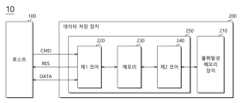
도 1은 본 발명의 실시 예에 따른 데이터 저장 장치(200)를 포함하는 데이터 처리 시스템(10)을 나타낸 도면이다.FIG. 1 is a drawing showing a data processing system (10) including a data storage device (200) according to an embodiment of the present invention.
도 1을 참조하면, 데이터 처리 시스템(10)은 호스트(100) 및 데이터 저장 장치(200)를 포함할 수 있다. 호스트(100)는 데이터 저장 장치(200)로 커맨드(CMD)를 전송할 수 있다. 데이터 저장 장치(200)는 호스트(100)로부터 수신된 커맨드(CMD)에 대응하는 동작을 수행하고, 수행 결과를 포함하는 응답(RES)을 호스트(100)로 전송할 수 있다. 또한, 호스트(100)와 데이터 저장 장치(200)는 데이터(DATA)를 송수신할 수 있다.Referring to FIG. 1, a data processing system (10) may include a host (100) and a data storage device (200). The host (100) may transmit a command (CMD) to the data storage device (200). The data storage device (200) may perform an operation corresponding to the command (CMD) received from the host (100) and transmit a response (RES) including the performance result to the host (100). In addition, the host (100) and the data storage device (200) may transmit and receive data (DATA).
호스트(100)는 휴대폰, MP3 플레이어, 랩탑 컴퓨터, 데스크탑 컴퓨터, 게임기, TV, 차량용 인포테인먼트(in-vehicle infotainment) 시스템 등을 포함할 수 있으나, 특별히 이에 한정되는 것은 아니다.The host (100) may include, but is not particularly limited to, a mobile phone, an MP3 player, a laptop computer, a desktop computer, a game console, a TV, an in-vehicle infotainment system, etc.
데이터 저장 장치(200)는 호스트(100)에 의해서 액세스되는 데이터를 저장할 수 있다. 데이터 저장 장치(200)는 호스트와 연결되는 인터페이스 프로토콜에 따라서 다양한 종류의 저장 장치들 중 어느 하나로 제조될 수 있다. 예를 들어, 데이터 저장 장치(200)는 솔리드 스테이트 드라이브(solid state drive, SSD), MMC, eMMC, RS-MMC, micro-MMC 형태의 멀티미디어 카드(multimedia card), SD, mini-SD, micro-SD 형태의 시큐어 디지털(secure digital) 카드, USB(universal storage bus) 저장 장치, UFS(universal flash storage) 장치, PCMCIA(personal computer memory card international association) 카드 형태의 저장 장치, PCI(peripheral component interconnection) 카드 형태의 저장 장치, PCI-E(PCI-express) 카드 형태의 저장 장치, CF(compact flash) 카드, 스마트 미디어(smart media) 카드, 메모리 스틱(memory stick) 등과 같은 다양한 종류의 저장 장치들 중 어느 하나로 구성될 수 있다.The data storage device (200) can store data accessed by the host (100). The data storage device (200) can be manufactured as any one of various types of storage devices according to an interface protocol connected to the host. For example, the data storage device (200) can be configured as any one of various types of storage devices, such as a solid state drive (SSD), a multimedia card in the form of an MMC, an eMMC, an RS-MMC, a micro-MMC, a secure digital card in the form of an SD, a mini-SD, a micro-SD, a universal storage bus (USB) storage device, a universal flash storage (UFS) device, a personal computer memory card international association (PCMCIA) card, a peripheral component interconnection (PCI) card, a PCI-E (PCI-express) card, a compact flash (CF) card, a smart media card, a memory stick, etc.
데이터 저장 장치(200)는 다양한 종류의 패키지(package) 형태들 중 어느 하나로 제조될 수 있다. 예를 들어, 데이터 저장 장치(200)는 POP(package on package), SIP(system in package), SOC(system on chip), MCP(multi chip package), COB(chip on board), WFP(wafer-level fabricated package), WSP(wafer-level stack package) 등과 같은 다양한 종류의 패키지 형태들 중 어느 하나로 제조될 수 있다.The data storage device (200) may be manufactured in any one of various types of package forms. For example, the data storage device (200) may be manufactured in any one of various types of package forms, such as a package on package (POP), a system in package (SIP), a system on chip (SOC), a multi chip package (MCP), a chip on board (COB), a wafer-level fabricated package (WFP), a wafer-level stack package (WSP), etc.
데이터 저장 장치(200)는 불휘발성 메모리 장치(210) 및 컨트롤러(250)를 포함할 수 있다.The data storage device (200) may include a nonvolatile memory device (210) and a controller (250).
불휘발성 메모리 장치(210)는 데이터 저장 장치(200)의 저장 매체로서 동작할 수 있다. 불휘발성 메모리 장치(210)는 메모리 셀에 따라서 낸드(NAND) 플래시 메모리 장치, 노어(NOR) 플래시 메모리 장치, 강유전체 커패시터를 이용한 강유전체 램(ferroelectric random access memory, FRAM), 티엠알(tunneling magneto-resistive, TMR) 막을 이용한 마그네틱 램(magnetic random access memory, MRAM), 칼코겐 화합물(chalcogenide alloys)을 이용한 상 변화 램(phase change random access memory, PRAM), 전이 금속 화합물(transition metal oxide)을 이용한 저항성 램(resistive random access memory, ReRAM) 등과 같은 다양한 형태의 불휘발성 메모리 장치들 중 어느 하나로 구성될 수 있다.The nonvolatile memory device (210) can operate as a storage medium of the data storage device (200). The nonvolatile memory device (210) can be configured as one of various types of nonvolatile memory devices, such as a NAND flash memory device, a NOR flash memory device, a ferroelectric random access memory (FRAM) using a ferroelectric capacitor, a magnetic random access memory (MRAM) using a tunneling magneto-resistive (TMR) film, a phase change random access memory (PRAM) using chalcogenide alloys, and a resistive random access memory (ReRAM) using a transition metal oxide, depending on the memory cell.
도면의 간략화를 위해, 도 1에서는 불휘발성 메모리 장치(210)를 하나의 블록으로 도시하였으나, 불휘발성 메모리 장치(210)는 복수의 메모리 칩들을 포함할 수 있다. 본 실시 예는 복수의 메모리 칩들로 구성된 불휘발성 메모리 장치(210)를 포함하는 데이터 저장 장치(200)에 대해서도 동일하게 적용될 수 있다.For simplicity of the drawing, the nonvolatile memory device (210) is illustrated as a single block in FIG. 1, but the nonvolatile memory device (210) may include a plurality of memory chips. The present embodiment may be equally applied to a data storage device (200) including a nonvolatile memory device (210) composed of a plurality of memory chips.
불휘발성 메모리 장치(210)는 복수의 비트라인들(도시되지 않음) 및 복수의 워드라인들(도시되지 않음)이 교차하는 영역들에 각각 배치되는 복수의 메모리 셀들을 갖는 메모리 셀 어레이(도시되지 않음)를 포함할 수 있다. 메모리 셀 어레이는 복수의 메모리 블록들을 포함할 수 있고, 복수의 메모리 블록들은 각각 복수의 페이지들을 포함할 수 있다.A nonvolatile memory device (210) may include a memory cell array (not shown) having a plurality of memory cells, each of which is arranged in regions where a plurality of bit lines (not shown) and a plurality of word lines (not shown) intersect. The memory cell array may include a plurality of memory blocks, and each of the plurality of memory blocks may include a plurality of pages.
예를 들어, 메모리 셀 어레이의 각 메모리 셀은 하나의 비트를 저장하는 싱글 레벨 셀(single, level cell, SLC), 2 비트의 데이터를 저장할 수 있는 멀티 레벨 셀(multi level cell, MLC), 3 비트의 데이터를 저장할 수 있는 트리플 레벨 셀(triple level cell, TLC) 또는 4 비트의 데이터를 저장할 수 있는 쿼드 레벨 셀(quad level cell, QLC)일 수 있다. 메모리 셀 어레이는 싱글 레벨 셀, 멀티 레벨 셀, 트리플 레벨 셀, 및 쿼드 레벨 셀 중 적어도 하나 이상을 포함할 수 있다. 예를 들어, 메모리 셀 어레이는 2차원 수평 구조의 메모리 셀들을 포함할 수도 있고, 또는 3차원 수직 구조의 메모리 셀들을 포함할 수도 있다.For example, each memory cell of the memory cell array may be a single-level cell (SLC) that stores one bit, a multi-level cell (MLC) that can store two bits of data, a triple-level cell (TLC) that can store three bits of data, or a quad-level cell (QLC) that can store four bits of data. The memory cell array may include at least one of the single-level cell, the multi-level cell, the triple-level cell, and the quad-level cell. For example, the memory cell array may include memory cells having a two-dimensional horizontal structure, or may include memory cells having a three-dimensional vertical structure.
컨트롤러(250)는 데이터 저장 장치(200)의 제반 동작을 제어할 수 있다. 컨트롤러(250)는 호스트로부터 수신된 커맨드(CMD)를 처리할 수 있다. 컨트롤러(200)는 호스트로부터 수신된 커맨드(CMD)에 근거하여 불휘발성 메모리 장치(210)의 동작을 제어하기 위한 제어 신호들을 생성하고, 생성된 제어 신호들을 불휘발성 메모리 장치(210)로 제공할 수 있다. 컨트롤러(250)는 제1 코어(220), 메모리(230) 및 제2 코어(240)를 포함할 수 있다.The controller (250) can control all operations of the data storage device (200). The controller (250) can process a command (CMD) received from a host. The controller (200) can generate control signals for controlling the operation of the nonvolatile memory device (210) based on the command (CMD) received from the host, and provide the generated control signals to the nonvolatile memory device (210). The controller (250) can include a first core (220), a memory (230), and a second core (240).
제1 코어(220)는 호스트(100)의 프로토콜에 대응하여 호스트와 데이터 저장 장치(200) 사이를 인터페이싱하도록 구성될 수 있다. 이에 따라, 제1 코어(220)는 프로토콜 코어(protocol core)로도 불릴 수 있다. 예를 들어, 제1 코어(220)는 USB(universal serial bus), UFS(universal flash storage), MMC(multimedia card), PATA(parallel advanced technology attachment), SATA(serial advanced technology attachment), SCSI(small computer system interface), SAS(serial attached SCSI), PCI(peripheral component interconnection), PCI-E(PCI express) 프로토콜 중 어느 하나를 통해 호스트와 통신할 수 있다.The first core (220) may be configured to interface between the host and the data storage device (200) in response to a protocol of the host (100). Accordingly, the first core (220) may also be called a protocol core. For example, the first core (220) may communicate with the host through any one of a universal serial bus (USB), universal flash storage (UFS), multimedia card (MMC), parallel advanced technology attachment (PATA), serial advanced technology attachment (SATA), small computer system interface (SCSI), serial attached SCSI (SAS), peripheral component interconnection (PCI), and PCI express (PCI-E) protocol.
제1 코어(220)는 마이크로 컨트롤 유닛(micro control unit)(MCU), 중앙 처리 장치(central processing unit)(CPU)를 포함할 수 있다. 제1 코어(220)는 호스트(100)로부터 전송되는 커맨드(CMD)들을 수신하고, 수신된 커맨드들(CMD)을 제2 코어(240)로 제공할 수 있다.The first core (220) may include a micro control unit (MCU) and a central processing unit (CPU). The first core (220) may receive commands (CMD) transmitted from the host (100) and provide the received commands (CMD) to the second core (240).
또한, 제1 코어(220)는 호스트(100)로부터 수신된 데이터(예컨대, 라이트 데이터)를 메모리(220)의 라이트 버퍼(write buffer)에 저장할 수 있다. 이를 위해, 컨트롤러(250)는 호스트(100)로부터 수신된 라이트 데이터를 메모리(230)의 라이트 버퍼(write buffer)로 전송하기 위한 데이터 전송 블록(225, 도 3 참조)을 더 포함할 수 있다. 예를 들어, 데이터 전송 블록(225)은 제1 코어(220)로부터 수신된 제어 신호(Ctrl_dt)에 따라 호스트(100)로부터 수신된 라이트 데이터를 메모리(230)의 라이트 버퍼(write buffer)에 저장하도록 동작할 수 있다.In addition, the first core (220) may store data (e.g., write data) received from the host (100) in a write buffer of the memory (220). To this end, the controller (250) may further include a data transfer block (225, see FIG. 3) for transmitting the write data received from the host (100) to the write buffer of the memory (230). For example, the data transfer block (225) may operate to store the write data received from the host (100) in the write buffer of the memory (230) according to a control signal (Ctrl_dt) received from the first core (220).
또한, 제1 코어(220)는 데이터 전송 블록(225)을 이용하여 메모리(230)의 리드 버퍼(read buffer)에 저장된 데이터(예컨대, 리드 데이터)를 호스트(100)로 전송할 수 있다. 예를 들어, 데이터 전송 블록(220)은 제1 코어(210)로부터 수신된 제어 신호(Ctrl_dt)에 따라 메모리(230)의 리드 버퍼(read buffer)에 저장된 리드 데이터를 호스트(100)로 전송하도록 동작할 수 있다.In addition, the first core (220) can transmit data (e.g., read data) stored in a read buffer of the memory (230) to the host (100) using the data transfer block (225). For example, the data transfer block (220) can operate to transmit read data stored in a read buffer of the memory (230) to the host (100) according to a control signal (Ctrl_dt) received from the first core (210).
또한, 제1 코어(220)는 호스트(100)로부터 수신된 커맨드(CMD)에 근거하여 디스크립터(descriptor)를 생성하고, 생성된 디스크립터(descriptor)를 제2 코어(240)로 제공할 수 있다. 여기에서, 디스크립터(descriptor)는 제2 코어(240)가 호스트(100)로부터 수신된 커맨드(CMD)를 처리하는데 필요한 정보를 포함하는 작업 기술서일 수 있다. 본 실시 예에서, 제1 코어(220)는 호스트(100)로부터 수신되는 라이트 커맨드 및 언맵 커맨드 각각에 대한 라이트 디스크립터 및 언맵 디스크립터를 생성할 수 있다. 이때, 라이트 디스크립터와 언맵 디스크립터는 동일한 포맷(format)을 가질 수 있다.In addition, the first core (220) may generate a descriptor based on a command (CMD) received from the host (100) and provide the generated descriptor to the second core (240). Here, the descriptor may be a work description including information necessary for the second core (240) to process the command (CMD) received from the host (100). In the present embodiment, the first core (220) may generate a write descriptor and an unmap descriptor for each of a write command and an unmap command received from the host (100). At this time, the write descriptor and the unmap descriptor may have the same format.
메모리(230)는 정적 랜덤 액세스 메모리(SRAM)와 같은 랜덤 액세스 메모리로 구성될 수 있으나, 특별히 이에 한정되는 것은 아니다. 메모리(230)는 제1 코어(220) 및 제2 코어(240)와 물리적으로 그리고 전기적으로 연결될 수 있다. 메모리(230)는 제2 코어(240)에 의해서 구동되는 소프트웨어 즉, 펌웨어를 저장할 수 있다. 또한, 메모리(230)는 펌웨어의 구동에 필요한 데이터, 예를 들면, 메타 데이터를 저장할 수 있다. 즉, 메모리(230)는 제2 코어(240)의 동작 메모리(working memory)로서 동작할 수 있다.The memory (230) may be configured as a random access memory such as a static random access memory (SRAM), but is not particularly limited thereto. The memory (230) may be physically and electrically connected to the first core (220) and the second core (240). The memory (230) may store software driven by the second core (240), that is, firmware. In addition, the memory (230) may store data required for driving the firmware, for example, metadata. That is, the memory (230) may operate as a working memory of the second core (240).
또한, 메모리(230)는 호스트(100)로부터 불휘발성 메모리 장치(210)로 전송될 라이트 데이터 또는 불휘발성 메모리 장치(210)로부터 호스트(100)로 전송될 리드 데이터를 임시 저장하기 위한 버퍼(buffer)를 포함하도록 구성될 수 있다. 즉, 메모리(220)는 버퍼 메모리(buffer memory)로서 동작할 수 있다. 메모리(230)의 내부 구성에 대해서는 이후 도 2를 참조하여 상세히 설명한다.In addition, the memory (230) may be configured to include a buffer for temporarily storing write data to be transmitted from the host (100) to the nonvolatile memory device (210) or read data to be transmitted from the nonvolatile memory device (210) to the host (100). That is, the memory (220) may operate as a buffer memory. The internal configuration of the memory (230) will be described in detail later with reference to FIG. 2.
제2 코어(240)는 메모리(230)에 로딩된 펌웨어의 구동을 통해서 데이터 저장 장치(200)의 제반 동작을 제어할 수 있다. 제2 코어(240)는 펌웨어 또는 소프트웨어와 같은 코드 형태의 명령(instruction) 또는 알고리즘을 해독하고 구동할 수 있다. 이에 따라, 제2 코어(240)는 FTL(flash translation layer) 코어로도 불릴 수 있다. 제2 코어(240)는 마이크로 컨트롤 유닛(micro control unit)(MCU), 중앙 처리 장치(central processing unit)(CPU)를 포함할 수 있다.The second core (240) can control the overall operation of the data storage device (200) by driving the firmware loaded into the memory (230). The second core (240) can decode and drive instructions or algorithms in the form of codes such as firmware or software. Accordingly, the second core (240) can also be called an FTL (flash translation layer) core. The second core (240) can include a micro control unit (MCU) and a central processing unit (CPU).
제2 코어(240)는 제1 코어(220)를 통해 제공된 커맨드에 근거하여 불휘발성 메모리 장치(210)의 동작을 제어하기 위한 제어 신호들을 생성하고, 생성된 제어 신호들을 불휘발성 메모리 장치(210)로 제공할 수 있다. 제어 신호들은 불휘발성 메모리 장치(210)를 제어하기 위한 커맨드, 어드레스, 동작 제어 신호 등을 포함할 수 있다. 제2 코어(240)는 라이트 데이터를 불휘발성 메모리 장치(210)로 제공하거나, 불휘발성 메모리 장치(210)로부터 리드 데이터를 제공 받을 수 있다.The second core (240) can generate control signals for controlling the operation of the nonvolatile memory device (210) based on a command provided through the first core (220), and provide the generated control signals to the nonvolatile memory device (210). The control signals can include commands, addresses, operation control signals, etc. for controlling the nonvolatile memory device (210). The second core (240) can provide write data to the nonvolatile memory device (210) or receive read data from the nonvolatile memory device (210).
또한, 제2 코어(240)는 호스트(100)로부터 제공된 라이트 데이터를 ECC(error correction code) 인코딩하여 패리티(parity)를 생성하는 ECC 인코딩 동작 및 패리티(parity)를 이용하여 불휘발성 메모리 장치(100)로부터 독출된 리드 데이터에 포함된 에러를 검출 및 정정하는 ECC 디코딩 동작을 수행하는 ECC 회로를 포함할 수 있다.In addition, the second core (240) may include an ECC circuit that performs an ECC encoding operation that encodes write data provided from a host (100) with an ECC (error correction code) to generate parity, and an ECC decoding operation that detects and corrects errors included in read data read from a nonvolatile memory device (100) using the parity.
도 2는 도 1의 메모리(230)를 나타낸 도면이다.Figure 2 is a drawing showing the memory (230) of Figure 1.
도 2를 참조하면, 본 실시 예에 따른 메모리(230)는 크게 제1 영역 및 제2 영역으로 구분될 수 있으나, 특별히 이에 한정되는 것은 아니다. 예를 들어, 메모리(230)의 제1 영역은 제1 코어(220)에서 생성된 디스크립터(descriptor)들을 저장하도록 구성된 디스크립터 버퍼(descriptor buffer)를 포함할 수 있다. 또한, 메모리(230)의 제1 영역에는 제2 코어(240)에 의해 해석 및 구동되는 펌웨어 및 제2 코어(240)에서 연산 및 처리 동작을 수행하는데 필요한 메타 데이터 등이 저장될 수 있다. 메모리(230)의 제2 영역은 라이트 데이터, 리드 데이터, 맵 데이터 등을 임시 저장하기 위한 버퍼들을 포함할 수 있으나, 특별히 이에 한정되는 것은 아니다.Referring to FIG. 2, the memory (230) according to the present embodiment may be largely divided into a first region and a second region, but is not particularly limited thereto. For example, the first region of the memory (230) may include a descriptor buffer configured to store descriptors generated by the first core (220). In addition, the first region of the memory (230) may store firmware interpreted and driven by the second core (240) and metadata required for performing calculation and processing operations in the second core (240). The second region of the memory (230) may include buffers for temporarily storing write data, read data, map data, and the like, but is not particularly limited thereto.
메모리(230)의 제1 영역과 제1 및 제2 코어들(220, 240) 간의 거리는 메모리(230)의 제2 영역과 제1 및 제2 코어들(220, 240) 간의 거리보다 짧을 수 있으나, 특별히 이에 한정되는 것은 아니다. 메모리(230)의 제1 영역이 제1 및 제2 코어들(220, 240)에 물리적으로 가까운 위치에 있음에 따라 제1 코어(220) 및 제2 코어(240)는 필요한 데이터에 빠르게 액세스할 수 있다.The distance between the first region of the memory (230) and the first and second cores (220, 240) may be shorter than the distance between the second region of the memory (230) and the first and second cores (220, 240), but is not particularly limited thereto. Since the first region of the memory (230) is physically close to the first and second cores (220, 240), the first core (220) and the second core (240) can quickly access necessary data.
예를 들어, 메모리(230)의 제1 영역에는 플래시 변환 계층(flash translation layer, FTL)이 저장될 수 있다. 플래시 변환 계층(FTL)은 제2 코어(240)에 의해 구동되는 소프트웨어로서, 제2 코어(240)는 플래시 변환 계층(FTL)을 구동시켜 불휘발성 메모리 장치(210)의 고유 동작을 제어하고, 호스트(100)에 장치 호환성을 제공할 수 있다. 플래시 변환 계층(FTL)의 구동을 통해서, 호스트(100)는 데이터 저장 장치(200)를 하드 디스크와 같은 일반적인 저장 장치로 인식하고 사용할 수 있다.For example, a flash translation layer (FTL) may be stored in the first area of the memory (230). The flash translation layer (FTL) is software driven by the second core (240), and the second core (240) may drive the flash translation layer (FTL) to control the unique operation of the nonvolatile memory device (210) and provide device compatibility to the host (100). By driving the flash translation layer (FTL), the host (100) may recognize and use the data storage device (200) as a general storage device such as a hard disk.
플래시 변환 계층(FTL)은 여러 기능을 수행하기 위한 모듈들을 포함할 수 있다. 예를 들어, 플래시 변환 계층(FTL)은 리드 모듈, 라이트 모듈, 가비지 컬렉션 모듈, 웨어-레벨링 모듈, 배드 블록 관리 모듈, 맵 모듈 등을 포함할 수 있다. 플래시 변환 계층(FTL)은 불휘발성 메모리 장치(210)의 시스템 영역(도시되지 않음)에 저장될 수 있고, 데이터 저장 장치(200)가 파워-온 되면 불휘발성 메모리 장치(210)의 시스템 영역으로부터 독출되어 메모리(230)의 제1 영역에 로드될 수 있다. 또한, 메모리(230)의 제1 영역에 로드된 플래시 변환 계층(flash translation layer, FTL)은 제2 코어(240)의 내부 또는 외부에 별도로 구비된 제2 코어(240) 전용 메모리(도시하지 않음)에 로드될 수도 있다.The flash translation layer (FTL) may include modules for performing various functions. For example, the flash translation layer (FTL) may include a read module, a write module, a garbage collection module, a wear-leveling module, a bad block management module, a map module, etc. The flash translation layer (FTL) may be stored in a system area (not shown) of a nonvolatile memory device (210), and when the data storage device (200) is powered on, the FTL may be read from the system area of the nonvolatile memory device (210) and loaded into a first area of the memory (230). In addition, the flash translation layer (FTL) loaded into the first area of the memory (230) may be loaded into a second core (240) dedicated memory (not shown) separately provided inside or outside the second core (240).
또한, 메모리(230)의 제1 영역은 플래시 변환 계층(FTL)에 포함된 다양한 모듈들의 구동에 필요한 메타 데이터가 저장되는 메타 영역(meta region)을 포함할 수 있다. 또한, 메타 영역(meta region)에는 P2L(physical-to-logical) 테이블이 저장될 수 있다.Additionally, the first region of the memory (230) may include a meta region in which meta data required for driving various modules included in the flash translation layer (FTL) is stored. Additionally, a physical-to-logical (P2L) table may be stored in the meta region.
메모리(230)의 제2 영역은 라이트 버퍼(write buffer), 리드 버퍼(read buffer), 및 맵 업데이트 버퍼(map update buffer) 등을 포함할 수 있다.The second area of the memory (230) may include a write buffer, a read buffer, and a map update buffer.
라이트 버퍼(write buffer)는 호스트(100)로부터 불휘발성 메모리 장치(210)로 전송될 라이트 데이터를 임시 저장하도록 구성될 수 있다. 리드 버퍼(read buffer)는 불휘발성 메모리 장치(210)로부터 독출되어 호스트(100)로 전송될 리드 데이터를 임시 저장하도록 구성될 수 있다. 맵 업데이트 버퍼(map update buffer)는 맵핑 정보가 업데이트될 맵 세그먼트를 임시 저장하도록 구성될 수 있다.A write buffer may be configured to temporarily store write data to be transmitted from a host (100) to a nonvolatile memory device (210). A read buffer may be configured to temporarily store read data to be read from a nonvolatile memory device (210) and transmitted to the host (100). A map update buffer may be configured to temporarily store a map segment for which mapping information is to be updated.
도 3은 제1 코어(220)가 호스트(100)로부터 수신된 커맨드(CMD)들에 대한 디스크립터(descriptor)들을 생성 및 저장하고, 언맵 커맨드(CMD_U)에 대한 응답을 호스트(100)로 전송하는 것을 나타낸 도면이다.FIG. 3 is a diagram showing a first core (220) generating and storing descriptors for commands (CMDs) received from a host (100) and transmitting a response to an unmap command (CMD_U) to the host (100).
호스트(100)로부터 라이트 커맨드(CMD_W) 및 라이트 데이터(WD)가 수신되면(①), 제1 코어(220)는 수신된 라이트 커맨드(CMD_W)를 메일 박스(250)의 커맨드 큐(251)에 큐잉할 수 있다(②). 동시에 제1 코어(220)는 라이트 커맨드(CMD_W)에 근거하여 라이트 디스크립터(DESW)를 생성하고, 생성된 라이트 디스크립터(DESW)를 메모리(230)의 디스크립터 버퍼(descriptor buffer)에 저장할 수 있다(②). 또한, 데이터 전송 블록(225)은 제1 코어(220)로부터 제공된 제어 신호(Ctrl_dt)에 따라 호스트(100)로부터 수신된 라이트 데이터(WD)를 메모리(230)의 라이트 버퍼(write buffer)에 저장할 수 있다(②).When a write command (CMD_W) and write data (WD) are received from the host (100) (①), the first core (220) can queue the received write command (CMD_W) in the command queue (251) of the mailbox (250) (②). At the same time, the first core (220) can generate a write descriptor (DESW) based on the write command (CMD_W) and store the generated write descriptor (DESW) in a descriptor buffer of the memory (230) (②). In addition, the data transfer block (225) can store the write data (WD) received from the host (100) in a write buffer (write buffer) of the memory (230) according to a control signal (Ctrl_dt) provided from the first core (220) (②).
이후, 호스트(100)로부터 언맵 커맨드(CMD_U)가 수신되면(③), 제1 코어(220)는 수신된 언맵 커맨드(CMD_U)를 메일 박스(250)의 커맨드 큐(251)에 큐잉하고(④), 언맵 커맨드(CMD_U)에 근거하여 언맵 디스크립터(DESU)를 생성하여 메모리(230)의 디스크립터 버퍼(descriptor buffer)에 저장할 수 있다(④). 또한, 제1 코어(220)는 언맵 디스크립터(DESU)를 메모리(230)의 디스크립터 버퍼(descriptor buffer)에 저장한 후 언맵 커맨드(CMD_U)에 대한 응답 신호(RES_U)를 호스트(100)로 전송할 수 있다(⑤).Thereafter, when an unmap command (CMD_U) is received from the host (100) (③), the first core (220) can queue the received unmap command (CMD_U) in the command queue (251) of the mailbox (250) (④), and generate an unmap descriptor (DESU) based on the unmap command (CMD_U) and store it in a descriptor buffer of the memory (230) (④). In addition, the first core (220) can transmit a response signal (RES_U) to the unmap command (CMD_U) to the host (100) after storing the unmap descriptor (DESU) in the descriptor buffer of the memory (230) (⑤).
이와 같이, 제1 코어(220)는 언맵 커맨드(CMD_U)에 대한 응답 신호(RES_U)를 언맵 캐싱 동작의 수행 여부에 관계 없이 언맵 디스크립터(DESU)를 메모리(230)의 디스크립터 버퍼(descriptor buffer)에 저장하는 즉시 호스트(100)로 전송한다. 이에 따라, 호스트(100) 측에서 측정되는 언맵 레이턴시(unmap latenty)를 줄일 수 있다.In this way, the first core (220) transmits a response signal (RES_U) to the unmap command (CMD_U) to the host (100) immediately after storing the unmap descriptor (DESU) in the descriptor buffer of the memory (230), regardless of whether or not the unmap caching operation is performed. Accordingly, the unmap latency measured on the host (100) side can be reduced.
호스트(100)는 데이터 저장 장치(200)로 동기(synchronous) 방식이 아닌 비동기(asynchronous) 방식으로 커맨드를 전송할 수 있다. 여기에서, 동기(synchronous) 방식은 데이터 저장 장치(200)로부터 이전 커맨드에 대한 응답 신호가 수신되면, 다음 커맨드를 전송하는 방식을 의미한다. 또한, 비동기(asynchronous) 방식은 데이터 저장 장치(200)로부터 응답 신호가 수신되는지 여부에 관계 없이 다음 커맨드를 전송하는 방식을 의미한다. 이에 따라, 언맵(unmap) 동작의 레이턴시(latency) 외에 언맵 커맨드 이전에 전송된 적어도 하나 이상의 커맨드에 대한 레이턴시가 모두 누적되어 언맵 커맨드에 대한 레이턴시로 측정되는 문제가 발생한다. 또한, 호스트(100)로부터 수신된 커맨드를 처리하는 도중 데이터 저장 장치(200) 내에서 백그라운드 동작(예컨대, 가비지 컬렉션 등)이 수행되는 경우 언맵 커맨드에 대한 레이턴시가 더욱 증가한다.The host (100) can transmit a command to the data storage device (200) in an asynchronous manner rather than a synchronous manner. Here, the synchronous manner means a manner in which the next command is transmitted when a response signal to a previous command is received from the data storage device (200). In addition, the asynchronous manner means a manner in which the next command is transmitted regardless of whether a response signal is received from the data storage device (200). Accordingly, in addition to the latency of the unmap operation, a problem occurs in which the latency for at least one command transmitted before the unmap command is accumulated and measured as the latency for the unmap command. In addition, if a background operation (e.g., garbage collection, etc.) is performed within the data storage device (200) while processing the command received from the host (100), the latency for the unmap command further increases.
이에 따라, 본 실시 예에서는 도 3에 도시한 바와 같이, 언맵 커맨드에 대한 응답 신호를 제2 코어(240)가 아닌 제1 코어(220)가 언맵 디스크립터를 생성한 후 즉시 호스트(100)로 전송하도록 함으로써, 호스트(100)에서 측정되는 언맵 커맨드에 대한 레이턴시가 증가하는 문제를 해결할 수 있다.Accordingly, in the present embodiment, as illustrated in FIG. 3, the problem of increased latency for the unmap command measured by the host (100) can be solved by having the first core (220), not the second core (240), transmit a response signal for the unmap command to the host (100) immediately after generating the unmap descriptor.
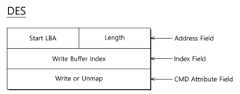
도 4는 제1 코어(220)가 생성하는 디스크립터(descriptor)의 포맷을 나타낸 도면이다.Figure 4 is a diagram showing the format of a descriptor generated by the first core (220).
전술한 바와 같이, 제1 코어(220)는 호스트(100)로부터 수신된 라이트 커맨드 및 언맵 커맨드 각각에 대한 디스크립터를 생성할 수 있다. 이때, 제1 코어(220)는 라이트 커맨드에 대한 디스크립터(즉, 라이트 디스크립터)와 언맵 커맨드에 대한 디스크립터(즉, 언맵 디스크립터)를 동일한 포맷으로 생성할 수 있다. 도 4를 참조하면, 제1 코어(220)가 생성하는 디스크립터(DES)는 어드레스 필드(address field), 인덱스 필드(index field) 및 커맨드 속성 필드(CMD attribute field)를 포함할 수 있다.As described above, the first core (220) can generate a descriptor for each of the write command and the unmap command received from the host (100). At this time, the first core (220) can generate the descriptor for the write command (i.e., the write descriptor) and the descriptor for the unmap command (i.e., the unmap descriptor) in the same format. Referring to FIG. 4, the descriptor (DES) generated by the first core (220) can include an address field, an index field, and a command attribute field (CMD attribute field).
디스크립터(DES)의 어드레스 필드에는 커맨드에 대한 시작 논리 블록 어드레스(Start LBA) 및 길이 정보(length)가 저장될 수 있다. 인덱스 필드에는 라이트 데이터가 저장된 라이트 버퍼(write buffer)의 인덱스가 저장될 수 있다. 커맨드 속성 필드에는 커맨드의 타입 즉, 라이트 커맨드인지 또는 언맵 커맨드인지를 나타내는 값이 저장될 수 있다.The address field of the descriptor (DES) can store the start logical block address (Start LBA) and length information (length) for the command. The index field can store the index of the write buffer where the write data is stored. The command attribute field can store a value indicating the type of the command, i.e., whether it is a write command or an unmap command.
라이트 디스크립터는 어드레스 필드, 인덱스 필드 및 커맨드 속성 필드에 각각 대응하는 값들이 저장될 수 있다. 언맵 디스크립터는 어드레스 필드 및 커맨드 속성 필드에는 대응하는 값들이 저장되고, 인덱스 필드에는 어떤 값도 저장되지 않을 수 있다.A light descriptor may store corresponding values in the address field, index field, and command attribute field, respectively. An unmap descriptor may store corresponding values in the address field and command attribute field, and may not store any value in the index field.
도 5a는 제2 코어(240)가 라이트 디스크립터(DESW)에 근거하여 라이트 동작을 수행하는 것을 나타낸 도면이고, 도 5b는 제2 코어(240)가 언맵 디스크립터(DESU)에 근거하여 언맵 캐싱 동작을 수행하는 것을 나타낸 도면이다. 설명의 편의를 위해, 라이트 커맨드에 대한 논리 블록 어드레스들과 언맵 커맨드에 대한 논리 블록 어드레스들이 동일한 것으로 가정한다. 또한, 라이트 동작을 수행한 후 언맵 캐싱 동작을 수행하는 것으로 가정한다.FIG. 5a is a diagram showing that the second core (240) performs a write operation based on a write descriptor (DESW), and FIG. 5b is a diagram showing that the second core (240) performs an unmap caching operation based on an unmap descriptor (DESU). For convenience of explanation, it is assumed that logical block addresses for a write command and logical block addresses for an unmap command are the same. In addition, it is assumed that the unmap caching operation is performed after performing the write operation.
제2 코어(240)는 메일 박스(250)의 커맨드 큐(251)를 주기적으로 폴링(polling)할 수 있다. 도 3에 도시한 바와 같이, 제1 코어(220)가 메일 박스(250)의 커맨드 큐(251)에 라이트 커맨드(CMD_W) 및 언맵 커맨드(CMD_U)를 순차적으로 큐잉한 것으로 가정하면, 제2 코어(240)는 커맨드 큐(251)로부터 라이트 커맨드(CMD_W)부터 디큐잉할 수 있다(①).The second core (240) can periodically poll the command queue (251) of the mailbox (250). As shown in FIG. 3, assuming that the first core (220) sequentially queues a write command (CMD_W) and an unmap command (CMD_U) to the command queue (251) of the mailbox (250), the second core (240) can dequeue the write command (CMD_W) from the command queue (251) (①).
제2 코어(240)는 메일 박스(250)의 커맨드 큐(251)로부터 디큐잉된 커맨드가 라이트 커맨드임을 확인하고, 메모리(230)의 디스크립터 버퍼를 액세스하여 라이트 디스크립터(DESW)를 리드할 수 있다(②). 제2 코어(240)는 리드한 라이트 디스크립터(DESW)를 해석하여 라이트 데이터(WD)가 저장된 라이트 버퍼의 인덱스를 확인하고, 인덱스에 대응하는 라이트 버퍼의 위치에 액세스하여 라이트 데이터(WD)를 리드할 수 있다(③).The second core (240) can confirm that the command dequeued from the command queue (251) of the mailbox (250) is a write command, and can access the descriptor buffer of the memory (230) to read the write descriptor (DESW) (②). The second core (240) can interpret the read write descriptor (DESW) to confirm the index of the write buffer where the write data (WD) is stored, and can access the position of the write buffer corresponding to the index to read the write data (WD) (③).
예를 들어, 도 5a에 도시한 바와 같이, 라이트 디스크립터(DESW)의 인덱스 필드에 저장된 값이 ‘1’이면, 제2 코어(240)는 라이트 버퍼의 인덱스 ‘1’에 해당하는 위치에 액세스하여 라이트 데이터(WD)를 리드할 수 있다.For example, as illustrated in FIG. 5a, if the value stored in the index field of the light descriptor (DESW) is ‘1’, the second core (240) can access the location corresponding to the index ‘1’ of the light buffer to read the light data (WD).
또한, 제2 코어(240)는 라이트할 논리 블록 어드레스를 물리 블록 어드레스로 변환할 수 있다(③). 예를 들어, 라이트 디스크립터(DESW)의 어드레스 필드에 저장된 시작 논리 블록 어드레스 및 길이 정보가 각각 ‘LBA1’ 및 ‘6’인 경우, 제2 코어(240)는 메모리(230)의 P2L 테이블에 ‘LBA1 내지 LBA6’을 순차적으로 저장함으로써, ‘LBA1 내지 LBA6’을 대응하는 물리 블록 어드레스들(PBAs)로 변환할 수 있다. 이후, 제2 코어(240)는 변환된 물리 블록 어드레스들(PBAs)을 포함하는 라이트 커맨드(WCMD) 및 리드한 라이트 데이터(WD)를 불휘발성 메모리 장치(210)로 제공할 수 있다(④).In addition, the second core (240) can convert a logical block address to be written into a physical block address (③). For example, if the start logical block address and length information stored in the address field of the write descriptor (DESW) are ‘LBA1’ and ‘6’, respectively, the second core (240) can convert ‘LBA1 to LBA6’ into corresponding physical block addresses (PBAs) by sequentially storing ‘LBA1 to LBA6’ in the P2L table of the memory (230). Thereafter, the second core (240) can provide a write command (WCMD) including the converted physical block addresses (PBAs) and the read write data (WD) to the nonvolatile memory device (210) (④).
불휘발성 메모리 장치(210)는 제2 코어(240)로부터 수신된 라이트 커맨드(WCMD)에 근거하여 라이트 데이터(WD)를 저장하고, 라이트 동작 수행 결과를 포함하는 응답 신호(RES_W)를 제2 코어(240)로 제공할 수 있다(⑤). 제2 코어(240)는 불휘발성 메모리 장치(210)로부터 수신된 응답 신호(RES_W)를 메일 박스(250)의 응답 신호 큐(253)에 큐잉할 수 있다(⑥).The nonvolatile memory device (210) can store write data (WD) based on a write command (WCMD) received from the second core (240) and provide a response signal (RES_W) including a result of performing a write operation to the second core (240) (⑤). The second core (240) can queue the response signal (RES_W) received from the nonvolatile memory device (210) in a response signal queue (253) of a mailbox (250) (⑥).
이후, 도 5b를 참조하면, 제2 코어(240)는 커맨드 큐(251)로부터 언맵 커맨드(CMD_U)를 디큐잉할 수 있다(①). 제2 코어(240)는 메일 박스(250)의 커맨드 큐(251)로부터 디큐잉된 커맨드가 언맵 커맨드임을 확인하고, 메모리(230)의 디스크립터 버퍼에 액세스하여 언맵 디스크립터(DESU)를 리드할 수 있다(②). 제2 코어(240)는 리드한 언맵 디스크립터(DESU)를 해석하여 트림(trim) 처리될 논리 블록 어드레스들을 확인한 후, 메모리(230)의 P2L 테이블에 언맵 정보를 저장하는 언맵 캐싱 동작을 수행할 수 있다(③).Thereafter, referring to FIG. 5b, the second core (240) can dequeue an unmap command (CMD_U) from the command queue (251) (①). The second core (240) can confirm that the command dequeued from the command queue (251) of the mailbox (250) is an unmap command, and can access the descriptor buffer of the memory (230) to read the unmap descriptor (DESU) (②). The second core (240) can interpret the read unmap descriptor (DESU) to confirm logical block addresses to be trimmed, and then perform an unmap caching operation to store unmap information in the P2L table of the memory (230) (③).
예를 들어, 도 5b에 도시한 바와 같이, 언맵 디스크립터(DESU)의 어드레스 필드에 저장된 시작 논리 블록 어드레스 및 길이 정보가 각각 ‘LBA1’ 및 ‘6’이면, 제2 코어(240)는 ‘LBA1 내지 LBA6’을 트림(trim) 처리 대상 논리 블록 어드레스들로 판단할 수 있다. 이에 따라, 제2 코어(240)는 ‘LBA1 내지 LBA6’ 각각의 트림(trim) 비트를 셋(set) 상태로 변경하고, 트림(trim) 비트가 변경된 ‘LBA1T 내지 LBA6T’을 메모리(230)의 P2L 테이블에 순차적으로 저장할 수 있다. 이후, 맵 업데이트 동작이 트리거되면, ‘LBA1 내지 LBA6’각각의 맵핑 정보는 우선 대응하는 물리 블록 어드레스들(PBAs)로 변경되었다가 이후 트림(trim) 처리될 것이다.For example, as illustrated in FIG. 5b, if the start logical block address and length information stored in the address field of the unmapped descriptor (DESU) are 'LBA1' and '6', respectively, the second core (240) may determine 'LBA1 to LBA6' as logical block addresses to be trimmed. Accordingly, the second core (240) may change the trim bit of each of 'LBA1 to LBA6' to a set state, and sequentially store 'LBA1T to LBA6T ' with the changed trim bit in the P2L table of the memory (230). Thereafter, when the map update operation is triggered, the mapping information of each of 'LBA1 to LBA6' will first be changed to corresponding physical block addresses (PBAs) and then be trimmed.
도 6a는 라이트 디스크립터에 포함된 논리 블록 어드레스가 리드 요청된 논리 블록 어드레스와 동일한 경우의 리드 동작을 나타낸 도면이고, 도 6b는 언맵 디스크립터에 포함된 논리 블록 어드레스가 리드 요청된 논리 블록 어드레스와 동일한 경우의 리드 동작을 나타낸 도면이다. 설명의 편의를 위해, 호스트(100)로부터 리드 커맨드(CMD_R)가 수신된 이후에 복수의 라이트 커맨드들과 언맵 커맨드가 수신된 것으로 가정한다.FIG. 6a is a diagram showing a read operation when a logical block address included in a write descriptor is identical to a read-requested logical block address, and FIG. 6b is a diagram showing a read operation when a logical block address included in an unmap descriptor is identical to a read-requested logical block address. For convenience of explanation, it is assumed that a plurality of write commands and an unmap command are received after a read command (CMD_R) is received from a host (100).
우선, 도 6a를 참조하면, 제2 코어(240)는 커맨드 큐(251)로부터 리드 커맨드(CMD_R)를 디큐잉할 수 있다(①). 리드 커맨드(CMD_R)는 리드할 논리 블록 어드레스들을 포함할 수 있다. 제2 코어(240)는 메모리(230)의 디스크립터 버퍼를 참조하여 리드할 논리 블록 어드레스와 동일한 논리 블록 어드레스를 갖는 디스크립터가 존재하는지 여부를 확인할 수 있다(②). 이때, 제2 코어(240)는 디스크립터 버퍼에 가장 최근에 저장된 디스크립터부터 확인할 수 있다.First, referring to FIG. 6a, the second core (240) can dequeue a read command (CMD_R) from the command queue (251) (①). The read command (CMD_R) can include logical block addresses to be read. The second core (240) can refer to the descriptor buffer of the memory (230) to check whether there is a descriptor having the same logical block address as the logical block address to be read (②). At this time, the second core (240) can check from the descriptor most recently stored in the descriptor buffer.
예를 들어, 언맵 디스크립터(DESU)와 제3 라이트 디스크립터(DESW3)가 리드할 논리 블록 어드레스와 동일한 논리 블록 어드레스를 포함하는 경우, 제2 코어(240)는 제3 라이트 디스크립터(DESW3)를 해석한 후 리드할 데이터가 라이트 버퍼에 저장된 것으로 판단할 수 있다. 제2 코어(240)는 별도로 구비된 데이터 전송 블록(245)으로 제어 신호(Ctrl_dt)를 제공할 수 있다(③).For example, if the unmap descriptor (DESU) and the third write descriptor (DESW3) include the same logical block address as the logical block address to be read, the second core (240) can determine that the data to be read is stored in the write buffer after interpreting the third write descriptor (DESW3). The second core (240) can provide a control signal (Ctrl_dt) to a separately provided data transfer block (245) (③).
데이터 전송 블록(245)은 제2 코어(240)로부터 수신된 제어 신호(Ctrl_dt)에 따라 라이트 버퍼로부터 제3 라이트 데이터(WD3)를 리드하고(④), 리드한 제3 라이트 데이터(WD3)를 리드 데이터(RD)로서 리드 버퍼에 저장할 수 있다(⑤). 이후, 제2 코어(240)는 리드 커맨드(CMD_R)에 대한 리드 동작 수행 결과를 포함하는 응답 신호(RES_R)를 메일 박스(250)의 응답 신호 큐(253)에 큐잉할 수 있다(⑥).The data transmission block (245) can read third write data (WD3) from the write buffer according to the control signal (Ctrl_dt) received from the second core (240) (④), and store the read third write data (WD3) as read data (RD) in the read buffer (⑤). Thereafter, the second core (240) can queue a response signal (RES_R) including the result of performing a read operation for the read command (CMD_R) in the response signal queue (253) of the mailbox (250) (⑥).
제1 코어(220)는 응답 신호 큐(253)에 큐잉된 응답 신호(RES_R)를 디큐잉하고(⑦), 응답 신호(RES_R)에 근거하여 데이터 전송 블록(225)으로 제어 신호(Ctrl_dt)를 제공할 수 있다(⑧). 데이터 전송 블록(225)은 제1 코어(220)로부터 수신된 제어 신호(Ctrl_dt)에 따라 리드 버퍼에 저장된 리드 데이터를 독출하여(⑨) 호스트(100)로 전송할 수 있다(⑩).The first core (220) can dequeue a response signal (RES_R) queued in a response signal queue (253) (⑦) and provide a control signal (Ctrl_dt) to the data transmission block (225) based on the response signal (RES_R) (⑧). The data transmission block (225) can read out read data stored in the read buffer (⑨) and transmit it to the host (100) according to the control signal (Ctrl_dt) received from the first core (220) (⑩).
한편, 도 6b를 참조하면, 제2 코어(240)는 커맨드 큐(251)로부터 리드 커맨드(CMD_R)를 디큐잉할 수 있다(①). 리드 커맨드(CMD_R)는 리드할 논리 블록 어드레스들을 포함할 수 있다. 제2 코어(240)는 메모리(230)의 디스크립터 버퍼를 참조하여 리드할 논리 블록 어드레스와 동일한 논리 블록 어드레스를 갖는 디스크립터가 존재하는지 여부를 확인할 수 있다(②).Meanwhile, referring to FIG. 6b, the second core (240) can dequeue a read command (CMD_R) from the command queue (251) (①). The read command (CMD_R) can include logical block addresses to be read. The second core (240) can refer to the descriptor buffer of the memory (230) to check whether there is a descriptor having the same logical block address as the logical block address to be read (②).
이때, 디스크립터 버퍼에 가장 최근에 저장된 디스크립터가 언맵 디스크립터(DESU)이고, 언맵 디스크립터(DESU)가 리드할 논리 블록 어드레스와 동일한 논리 블록 어드레스를 포함하는 경우, 제2 코어(240)는 리드할 논리 블록 어드레스들은 무효인 논리 블록 어드레스임을 나타내는 정보가 포함된 응답 신호(RES_IVL)를 응답 신호 큐(253)에 큐잉할 수 있다(③).At this time, if the descriptor most recently stored in the descriptor buffer is an unmapped descriptor (DESU) and the unmapped descriptor (DESU) includes a logical block address that is identical to the logical block address to be read, the second core (240) can queue a response signal (RES_IVL) including information indicating that the logical block addresses to be read are invalid logical block addresses in the response signal queue (253) (③).
제1 코어(220)는 응답 신호 큐(253)에 큐잉된 응답 신호(RES_IVL)를 디큐잉하고(④), 응답 신호(RES_IVL)에 근거하여 호스트(100)로 리드 커맨드(CMD_R)에 대한 논리 블록 어드레스는 무효인 논리 블록 어드레스임을 나타내는 신호(RES_IVL)를 전송한다(⑤).The first core (220) dequeues a response signal (RES_IVL) queued in the response signal queue (253) (④), and transmits a signal (RES_IVL) indicating that the logical block address for the read command (CMD_R) to the host (100) is an invalid logical block address based on the response signal (RES_IVL) (⑤).
도 7은 본 실시 예에 따른 데이터 저장 장치의 동작 방법을 나타낸 순서도이다. 도 7을 참조하여 본 실시 예에 따른 데이터 저장 장치의 동작 방법을 설명함에 있어서, 도 1 내지 도 6b 중 적어도 하나의 도면이 참조될 수 있다.FIG. 7 is a flowchart illustrating an operation method of a data storage device according to the present embodiment. When explaining the operation method of a data storage device according to the present embodiment with reference to FIG. 7, at least one of FIGS. 1 to 6b may be referenced.
S710 단계에서, 데이터 저장 장치(200)의 컨트롤러(250)는 호스트(100)로부터 언맵 커맨드를 수신할 수 있다.At step S710, the controller (250) of the data storage device (200) can receive an unmap command from the host (100).
S720 단계에서, 컨트롤러(250)의 제1 코어(220)는 호스트(100)로부터 수신된 언맵 커맨드에 근거하여 트림(trim) 처리할 논리 블록 어드레스를 포함하는 언맵 디스크립터를 생성하고, 메모리(230)의 디스크립터 버퍼에 저장할 수 있다.At step S720, the first core (220) of the controller (250) may generate an unmap descriptor including a logical block address to be trimmed based on an unmap command received from the host (100) and store it in a descriptor buffer of the memory (230).
S730 단계에서, 제1 코어(220)는 언맵 커맨드에 대한 언맵 캐싱 동작이 완료되었음을 나타내는 응답 신호를 호스트(100)로 전송할 수 있다.At step S730, the first core (220) may transmit a response signal to the host (100) indicating that the unmap caching operation for the unmap command has been completed.
도 7에는 도시하지 않았으나, 호스트(100)로 응답 신호를 전송한 후, 제2 코어(240)가 메일 박스(250)의 커맨드 큐(251)로부터 언맵 커맨드를 디큐잉하고, 디큐잉한 언맵 커맨드에 대응하는 언맵 디스크립터를 메모리(230)의 디스크립터 버퍼로부터 리드하여 해석하고, 트림(trim) 처리할 논리 블록 어드레스들에 대한 언맵 캐싱 동작을 수행할 수 있다.Although not shown in FIG. 7, after transmitting a response signal to the host (100), the second core (240) can dequeue an unmap command from the command queue (251) of the mailbox (250), read an unmap descriptor corresponding to the dequeued unmap command from the descriptor buffer of the memory (230), interpret it, and perform an unmap caching operation on logical block addresses to be trimmed.
도 8은 본 발명의 실시 예에 따른 솔리드 스테이트 드라이브(SSD)를 포함하는 데이터 처리 시스템을 예시적으로 나타낸 도면이다. 도 8을 참조하면, 데이터 처리 시스템(2000)은 호스트 장치(2100)와 솔리드 스테이트 드라이브(solid state drive)(2200)(이하, SSD라 칭함)를 포함할 수 있다.FIG. 8 is a diagram exemplarily illustrating a data processing system including a solid state drive (SSD) according to an embodiment of the present invention. Referring to FIG. 8, a data processing system (2000) may include a host device (2100) and a solid state drive (2200) (hereinafter, referred to as SSD).
SSD(2200)는 컨트롤러(2210), 버퍼 메모리 장치(2220), 불휘발성 메모리 장치들(2231~223n), 전원 공급기(2240), 신호 커넥터(2250) 및 전원 커넥터(2260)를 포함할 수 있다.The SSD (2200) may include a controller (2210), a buffer memory device (2220), nonvolatile memory devices (2231 to 223n), a power supply (2240), a signal connector (2250), and a power connector (2260).
컨트롤러(2210)는 SSD(2200)의 제반 동작을 제어할 수 있다.The controller (2210) can control all operations of the SSD (2200).
버퍼 메모리 장치(2220)는 불휘발성 메모리 장치들(2231~223n)에 저장될 데이터를 임시 저장할 수 있다. 또한, 버퍼 메모리 장치(2220)는 불휘발성 메모리 장치들(2231~223n)로부터 읽혀진 데이터를 임시 저장할 수 있다. 버퍼 메모리 장치(2220)에 임시 저장된 데이터는 컨트롤러(2210)의 제어에 따라 호스트 장치(2100) 또는 불휘발성 메모리 장치들(2231~223n)로 전송될 수 있다.The buffer memory device (2220) can temporarily store data to be stored in the nonvolatile memory devices (2231 to 223n). In addition, the buffer memory device (2220) can temporarily store data read from the nonvolatile memory devices (2231 to 223n). The data temporarily stored in the buffer memory device (2220) can be transmitted to the host device (2100) or the nonvolatile memory devices (2231 to 223n) under the control of the controller (2210).
불휘발성 메모리 장치들(2231~223n)은 SSD(2200)의 저장 매체로 사용될 수 있다. 불휘발성 메모리 장치들(2231~223n) 각각은 복수의 채널들(CH1~CHn)을 통해 컨트롤러(2210)와 연결될 수 있다. 하나의 채널에는 하나 또는 그 이상의 불휘발성 메모리 장치가 연결될 수 있다. 하나의 채널에 연결되는 불휘발성 메모리 장치들은 동일한 신호 버스 및 데이터 버스에 연결될 수 있다.Nonvolatile memory devices (2231 to 223n) can be used as a storage medium of the SSD (2200). Each of the nonvolatile memory devices (2231 to 223n) can be connected to the controller (2210) through a plurality of channels (CH1 to CHn). One or more nonvolatile memory devices can be connected to one channel. The nonvolatile memory devices connected to one channel can be connected to the same signal bus and data bus.
전원 공급기(2240)는 전원 커넥터(2260)를 통해 입력된 전원(PWR)을 SSD(2200) 내부에 제공할 수 있다. 전원 공급기(2240)는 보조 전원 공급기(2241)를 포함할 수 있다. 보조 전원 공급기(2241)는 서든 파워 오프(sudden power off)가 발생되는 경우, SSD(2200)가 정상적으로 종료될 수 있도록 전원을 공급할 수 있다. 보조 전원 공급기(2241)는 전원(PWR)을 충전할 수 있는 대용량 캐패시터들(capacitors)을 포함할 수 있다.The power supply (2240) can provide power (PWR) input through the power connector (2260) to the inside of the SSD (2200). The power supply (2240) can include an auxiliary power supply (2241). The auxiliary power supply (2241) can supply power so that the SSD (2200) can be normally shut down when a sudden power off occurs. The auxiliary power supply (2241) can include large-capacity capacitors that can charge the power (PWR).
컨트롤러(2210)는 신호 커넥터(2250)를 통해서 호스트 장치(2100)와 신호(SGL)를 주고 받을 수 있다. 여기에서, 신호(SGL)는 커맨드, 어드레스, 데이터 등을 포함할 수 있다. 신호 커넥터(2250)는 호스트 장치(2100)와 SSD(2200)의 인터페이스 방식에 따라 다양한 형태의 커넥터로 구성될 수 있다.The controller (2210) can exchange signals (SGL) with the host device (2100) through the signal connector (2250). Here, the signal (SGL) can include a command, an address, data, etc. The signal connector (2250) can be configured as various types of connectors depending on the interface method of the host device (2100) and the SSD (2200).
도 9는 도 8의 컨트롤러의 구성을 예시적으로 나타낸 도면이다. 도 9를 참조하면, 컨트롤러(2210)는 호스트 인터페이스 유닛(2211), 컨트롤 유닛(2212), 랜덤 액세스 메모리(2213), 에러 정정 코드(ECC) 유닛(2214) 및 메모리 인터페이스 유닛(2215)을 포함할 수 있다.FIG. 9 is a diagram exemplarily showing the configuration of the controller of FIG. 8. Referring to FIG. 9, the controller (2210) may include a host interface unit (2211), a control unit (2212), a random access memory (2213), an error correction code (ECC) unit (2214), and a memory interface unit (2215).
호스트 인터페이스 유닛(2211)은, 호스트 장치(2100)의 프로토콜에 따라서, 호스트 장치(2100)와 SSD(2200)를 인터페이싱할 수 있다. 예를 들면, 호스트 인터페이스 유닛(2211)은, 시큐어 디지털(secure digital), USB(universal serial bus), MMC(multi-media card), eMMC(embedded MMC), PCMCIA(personal computer memory card international association), PATA(parallel advanced technology attachment), SATA(serial advanced technology attachment), SCSI(small computer system interface), SAS(serial attached SCSI), PCI(peripheral component interconnection), PCI-E(PCI Expresss), UFS(universal flash storage) 프로토콜들 중 어느 하나를 통해서 호스트 장치(2100)와 통신할 수 있다. 또한, 호스트 인터페이스 유닛(2211)은 호스트 장치(2100)가 SSD(2200)를 범용 데이터 저장 장치, 예를 들면, 하드 디스크 드라이브(HDD)로 인식하도록 지원하는 디스크 에뮬레이션(disk emulation) 기능을 수행할 수 있다.The host interface unit (2211) can interface the host device (2100) and the SSD (2200) according to the protocol of the host device (2100). For example, the host interface unit (2211) can communicate with the host device (2100) through any one of the secure digital, universal serial bus (USB), multi-media card (MMC), embedded MMC (eMMC), personal computer memory card international association (PCMCIA), parallel advanced technology attachment (PATA), serial advanced technology attachment (SATA), small computer system interface (SCSI), serial attached SCSI (SAS), peripheral component interconnection (PCI), PCI-E (PCI Expresses), and universal flash storage (UFS) protocols. Additionally, the host interface unit (2211) can perform a disk emulation function that supports the host device (2100) to recognize the SSD (2200) as a general-purpose data storage device, for example, a hard disk drive (HDD).
컨트롤 유닛(2212)은 호스트 장치(2100)로부터 입력된 신호(SGL)를 분석하고 처리할 수 있다. 컨트롤 유닛(2212)은 SSD(2200)를 구동하기 위한 펌웨어 또는 소프트웨어에 따라서 내부 기능 블럭들의 동작을 제어할 수 있다. 랜덤 액세스 메모리(2213)는 이러한 펌웨어 또는 소프트웨어를 구동하기 위한 동작 메모리로서 사용될 수 있다.The control unit (2212) can analyze and process a signal (SGL) input from the host device (2100). The control unit (2212) can control the operation of internal function blocks according to firmware or software for driving the SSD (2200). The random access memory (2213) can be used as an operating memory for driving such firmware or software.
에러 정정 코드(ECC) 유닛(2214)은 불휘발성 메모리 장치들(2231~223n)로 전송될 데이터의 패리티 데이터를 생성할 수 있다. 생성된 패리티 데이터는 데이터와 함께 불휘발성 메모리 장치들(2231~223n)에 저장될 수 있다. 에러 정정 코드(ECC) 유닛(2214)은 패리티 데이터에 근거하여 불휘발성 메모리 장치들(2231~223n)로부터 독출된 데이터의 에러를 검출할 수 있다. 만약, 검출된 에러가 정정 범위 내이면, 에러 정정 코드(ECC) 유닛(2214)은 검출된 에러를 정정할 수 있다.An error correction code (ECC) unit (2214) can generate parity data of data to be transmitted to nonvolatile memory devices (2231 to 223n). The generated parity data can be stored in the nonvolatile memory devices (2231 to 223n) together with the data. The error correction code (ECC) unit (2214) can detect an error in data read from the nonvolatile memory devices (2231 to 223n) based on the parity data. If the detected error is within a correction range, the error correction code (ECC) unit (2214) can correct the detected error.
메모리 인터페이스 유닛(2215)은, 컨트롤 유닛(2212)의 제어에 따라서, 불휘발성 메모리 장치들(2231~223n)에 커맨드 및 어드레스와 같은 제어 신호를 제공할 수 있다. 그리고 메모리 인터페이스 유닛(2215)은, 컨트롤 유닛(2212)의 제어에 따라서, 불휘발성 메모리 장치들(2231~223n)과 데이터를 주고받을 수 있다. 예를 들면, 메모리 인터페이스 유닛(2215)은 버퍼 메모리 장치(2220)에 저장된 데이터를 불휘발성 메모리 장치들(2231~223n)로 제공하거나, 불휘발성 메모리 장치들(2231~223n)로부터 읽혀진 데이터를 버퍼 메모리 장치(2220)로 제공할 수 있다.The memory interface unit (2215) can provide control signals, such as commands and addresses, to the nonvolatile memory devices (2231 to 223n) under the control of the control unit (2212). In addition, the memory interface unit (2215) can exchange data with the nonvolatile memory devices (2231 to 223n) under the control of the control unit (2212). For example, the memory interface unit (2215) can provide data stored in the buffer memory device (2220) to the nonvolatile memory devices (2231 to 223n) or provide data read from the nonvolatile memory devices (2231 to 223n) to the buffer memory device (2220).
도 10은 본 발명의 실시 예에 따른 데이터 저장 장치를 포함하는 데이터 처리 시스템을 예시적으로 나타낸 도면이다. 도 10을 참조하면, 데이터 처리 시스템(3000)은 호스트 장치(3100)와 데이터 저장 장치(3200)를 포함할 수 있다.FIG. 10 is a diagram exemplarily illustrating a data processing system including a data storage device according to an embodiment of the present invention. Referring to FIG. 10, a data processing system (3000) may include a host device (3100) and a data storage device (3200).
호스트 장치(3100)는 인쇄 회로 기판(printed circuit board)과 같은 기판(board) 형태로 구성될 수 있다. 비록 도시되지 않았지만, 호스트 장치(3100)는 호스트 장치의 기능을 수행하기 위한 내부 기능 블럭들을 포함할 수 있다.The host device (3100) may be configured in the form of a board, such as a printed circuit board. Although not shown, the host device (3100) may include internal function blocks for performing the functions of the host device.
호스트 장치(3100)는 소켓(socket), 슬롯(slot) 또는 커넥터(connector)와 같은 접속 터미널(3110)을 포함할 수 있다. 데이터 저장 장치(3200)는 접속 터미널(3110)에 마운트(mount)될 수 있다.The host device (3100) may include a connection terminal (3110), such as a socket, a slot, or a connector. The data storage device (3200) may be mounted on the connection terminal (3110).
데이터 저장 장치(3200)는 인쇄 회로 기판과 같은 기판 형태로 구성될 수 있다. 데이터 저장 장치(3200)는 메모리 모듈 또는 메모리 카드로 불릴 수 있다. 데이터 저장 장치(3200)는 컨트롤러(3210), 버퍼 메모리 장치(3220), 불휘발성 메모리 장치(3231~3232), PMIC(power management integrated circuit)(3240) 및 접속 터미널(3250)을 포함할 수 있다.The data storage device (3200) may be configured in the form of a substrate such as a printed circuit board. The data storage device (3200) may be called a memory module or a memory card. The data storage device (3200) may include a controller (3210), a buffer memory device (3220), a nonvolatile memory device (3231-3232), a PMIC (power management integrated circuit) (3240), and a connection terminal (3250).
컨트롤러(3210)는 데이터 저장 장치(3200)의 제반 동작을 제어할 수 있다. 컨트롤러(3210)는 도 9에 도시된 컨트롤러(2210)와 동일하게 구성될 수 있다.The controller (3210) can control all operations of the data storage device (3200). The controller (3210) can be configured identically to the controller (2210) illustrated in FIG. 9.
버퍼 메모리 장치(3220)는 불휘발성 메모리 장치들(3231~3232)에 저장될 데이터를 임시 저장할 수 있다. 또한, 버퍼 메모리 장치(3220)는 불휘발성 메모리 장치들(3231~3232)로부터 읽혀진 데이터를 임시 저장할 수 있다. 버퍼 메모리 장치(3220)에 임시 저장된 데이터는 컨트롤러(3210)의 제어에 따라 호스트 장치(3100) 또는 불휘발성 메모리 장치들(3231~3232)로 전송될 수 있다.The buffer memory device (3220) can temporarily store data to be stored in the nonvolatile memory devices (3231 to 3232). In addition, the buffer memory device (3220) can temporarily store data read from the nonvolatile memory devices (3231 to 3232). The data temporarily stored in the buffer memory device (3220) can be transmitted to the host device (3100) or the nonvolatile memory devices (3231 to 3232) under the control of the controller (3210).
불휘발성 메모리 장치들(3231~3232)은 데이터 저장 장치(3200)의 저장 매체로 사용될 수 있다.Nonvolatile memory devices (3231 to 3232) can be used as storage media of the data storage device (3200).
PMIC(3240)는 접속 터미널(3250)을 통해 입력된 전원을 데이터 저장 장치(3200) 내부에 제공할 수 있다. PMIC(3240)는, 컨트롤러(3210)의 제어에 따라서, 데이터 저장 장치(3200)의 전원을 관리할 수 있다.PMIC (3240) can provide power input through connection terminal (3250) to the inside of data storage device (3200). PMIC (3240) can manage power of data storage device (3200) under control of controller (3210).
접속 터미널(3250)은 호스트 장치의 접속 터미널(3110)에 연결될 수 있다. 접속 터미널(3250)을 통해서, 호스트 장치(3100)와 데이터 저장 장치(3200) 간에 커맨드, 어드레스, 데이터 등과 같은 신호와, 전원이 전달될 수 있다. 접속 터미널(3250)은 호스트 장치(3100)와 데이터 저장 장치(3200)의 인터페이스 방식에 따라 다양한 형태로 구성될 수 있다. 접속 터미널(3250)은 데이터 저장 장치(3200)의 어느 한 변에 배치될 수 있다.The connection terminal (3250) can be connected to the connection terminal (3110) of the host device. Through the connection terminal (3250), signals such as commands, addresses, data, etc., and power can be transmitted between the host device (3100) and the data storage device (3200). The connection terminal (3250) can be configured in various forms depending on the interface method between the host device (3100) and the data storage device (3200). The connection terminal (3250) can be arranged on either side of the data storage device (3200).
도 11은 본 발명의 실시 예에 따른 데이터 저장 장치를 포함하는 데이터 처리 시스템을 예시적으로 나타낸 도면이다. 도 11을 참조하면, 데이터 처리 시스템(4000)은 호스트 장치(4100)와 데이터 저장 장치(4200)를 포함할 수 있다.FIG. 11 is a diagram exemplarily illustrating a data processing system including a data storage device according to an embodiment of the present invention. Referring to FIG. 11, a data processing system (4000) may include a host device (4100) and a data storage device (4200).
호스트 장치(4100)는 인쇄 회로 기판(printed circuit board)과 같은 기판(board) 형태로 구성될 수 있다. 비록 도시되지 않았지만, 호스트 장치(4100)는 호스트 장치의 기능을 수행하기 위한 내부 기능 블럭들을 포함할 수 있다.The host device (4100) may be configured in the form of a board, such as a printed circuit board. Although not shown, the host device (4100) may include internal function blocks for performing the functions of the host device.
데이터 저장 장치(4200)는 표면 실장형 패키지 형태로 구성될 수 있다. 데이터 저장 장치(4200)는 솔더 볼(solder ball)(4250)을 통해서 호스트 장치(4100)에 마운트될 수 있다. 데이터 저장 장치(4200)는 컨트롤러(4210), 버퍼 메모리 장치(4220) 및 불휘발성 메모리 장치(4230)를 포함할 수 있다.The data storage device (4200) may be configured in a surface mount package form. The data storage device (4200) may be mounted to a host device (4100) via a solder ball (4250). The data storage device (4200) may include a controller (4210), a buffer memory device (4220), and a nonvolatile memory device (4230).
컨트롤러(4210)는 데이터 저장 장치(4200)의 제반 동작을 제어할 수 있다. 컨트롤러(4210)는 도 9에 도시된 컨트롤러(2210)와 동일하게 구성될 수 있다.The controller (4210) can control all operations of the data storage device (4200). The controller (4210) can be configured identically to the controller (2210) illustrated in FIG. 9.
버퍼 메모리 장치(4220)는 불휘발성 메모리 장치(4230)에 저장될 데이터를 임시 저장할 수 있다. 또한, 버퍼 메모리 장치(4220)는 불휘발성 메모리 장치들(4230)로부터 읽혀진 데이터를 임시 저장할 수 있다. 버퍼 메모리 장치(4220)에 임시 저장된 데이터는 컨트롤러(4210)의 제어에 따라 호스트 장치(4100) 또는 불휘발성 메모리 장치(4230)로 전송될 수 있다.The buffer memory device (4220) can temporarily store data to be stored in the nonvolatile memory device (4230). In addition, the buffer memory device (4220) can temporarily store data read from the nonvolatile memory devices (4230). The data temporarily stored in the buffer memory device (4220) can be transmitted to the host device (4100) or the nonvolatile memory device (4230) under the control of the controller (4210).
불휘발성 메모리 장치(4230)는 데이터 저장 장치(4200)의 저장 매체로 사용될 수 있다.A nonvolatile memory device (4230) can be used as a storage medium of a data storage device (4200).
도 12는 본 발명의 실시 예에 따른 데이터 저장 장치를 포함하는 네트워크 시스템(5000)을 예시적으로 나타낸 도면이다. 도 12는 참조하면, 네트워크 시스템(5000)은 네트워크(5500)를 통해서 연결된 서버 시스템(5300) 및 복수의 클라이언트 시스템들(5410~5430)을 포함할 수 있다.FIG. 12 is a diagram exemplarily showing a network system (5000) including a data storage device according to an embodiment of the present invention. Referring to FIG. 12, the network system (5000) may include a server system (5300) and a plurality of client systems (5410 to 5430) connected via a network (5500).
서버 시스템(5300)은 복수의 클라이언트 시스템들(5410~5430)의 요청에 응답하여 데이터를 서비스할 수 있다. 예를 들면, 서버 시스템(5300)은 복수의 클라이언트 시스템들(5410~5430)로부터 제공된 데이터를 저장할 수 있다. 다른 예로서, 서버 시스템(5300)은 복수의 클라이언트 시스템들(5410~5430)로 데이터를 제공할 수 있다.The server system (5300) can serve data in response to requests from multiple client systems (5410 to 5430). For example, the server system (5300) can store data provided from multiple client systems (5410 to 5430). As another example, the server system (5300) can provide data to multiple client systems (5410 to 5430).
서버 시스템(5300)은 호스트 장치(5100) 및 데이터 저장 장치(5200)를 포함할 수 있다. 데이터 저장 장치(5200)는 도 1의 데이터 저장 장치(10), 도 8의 데이터 저장 장치(2200), 도 10의 데이터 저장 장치(3200) 및 도 11의 데이터 저장 장치(4200)로 구성될 수 있다.The server system (5300) may include a host device (5100) and a data storage device (5200). The data storage device (5200) may be composed of the data storage device (10) of FIG. 1, the data storage device (2200) of FIG. 8, the data storage device (3200) of FIG. 10, and the data storage device (4200) of FIG. 11.
도 13은 본 발명의 실시 예에 따른 데이터 저장 장치에 포함된 불휘발성 메모리 장치를 예시적으로 보여주는 블록도이다. 도 13을 참조하면, 불휘발성 메모리 장치(100)는 메모리 셀 어레이(110), 행 디코더(120), 열 디코더(130), 데이터 읽기/쓰기 블럭(140), 전압 발생기(150) 및 제어 로직(160)을 포함할 수 있다.FIG. 13 is a block diagram exemplarily showing a nonvolatile memory device included in a data storage device according to an embodiment of the present invention. Referring to FIG. 13, a nonvolatile memory device (100) may include a memory cell array (110), a row decoder (120), a column decoder (130), a data read/write block (140), a voltage generator (150), and control logic (160).
메모리 셀 어레이(110)는 워드 라인들(WL1~WLm)과 비트 라인들(BL1~BLn)이 서로 교차된 영역에 배열된 메모리 셀(MC)들을 포함할 수 있다.The memory cell array (110) may include memory cells (MC) arranged in an area where word lines (WL1 to WLm) and bit lines (BL1 to BLn) intersect each other.
행 디코더(120)는 워드 라인들(WL1~WLm)을 통해서 메모리 셀 어레이(110)와 연결될 수 있다. 행 디코더(120)는 제어 로직(160)의 제어에 따라 동작할 수 있다. 행 디코더(120)는 외부 장치(도시되지 않음)로부터 제공된 어드레스를 디코딩할 수 있다. 행 디코더(120)는 디코딩 결과에 근거하여 워드 라인들(WL1~WLm)을 선택하고, 구동할 수 있다. 예시적으로, 행 디코더(120)는 전압 발생기(150)로부터 제공된 워드 라인 전압을 워드 라인들(WL1~WLm)에 제공할 수 있다.The row decoder (120) may be connected to the memory cell array (110) via word lines (WL1 to WLm). The row decoder (120) may operate under the control of the control logic (160). The row decoder (120) may decode an address provided from an external device (not shown). The row decoder (120) may select and drive the word lines (WL1 to WLm) based on the decoding result. For example, the row decoder (120) may provide a word line voltage provided from a voltage generator (150) to the word lines (WL1 to WLm).
데이터 읽기/쓰기 블럭(140)은 비트 라인들(BL1~BLn)을 통해서 메모리 셀 어레이(110)와 연결될 수 있다. 데이터 읽기/쓰기 블럭(140)은 비트 라인들(BL1~BLn) 각각에 대응하는 읽기/쓰기 회로들(RW1~RWn)을 포함할 수 있다. 데이터 읽기/쓰기 블럭(140)은 제어 로직(160)의 제어에 따라 동작할 수 있다. 데이터 읽기/쓰기 블럭(140)은 동작 모드에 따라서 쓰기 드라이버로서 또는 감지 증폭기로서 동작할 수 있다. 예를 들면, 데이터 읽기/쓰기 블럭(140)은 쓰기 동작 시 외부 장치로부터 제공된 데이터를 메모리 셀 어레이(110)에 저장하는 쓰기 드라이버로서 동작할 수 있다. 다른 예로서, 데이터 읽기/쓰기 블럭(140)은 읽기 동작 시 메모리 셀 어레이(110)로부터 데이터를 독출하는 감지 증폭기로서 동작할 수 있다.The data read/write block (140) may be connected to the memory cell array (110) via bit lines (BL1 to BLn). The data read/write block (140) may include read/write circuits (RW1 to RWn) corresponding to each of the bit lines (BL1 to BLn). The data read/write block (140) may operate under the control of the control logic (160). The data read/write block (140) may operate as a write driver or a sense amplifier depending on the operation mode. For example, the data read/write block (140) may operate as a write driver that stores data provided from an external device in the memory cell array (110) during a write operation. As another example, the data read/write block (140) may operate as a sense amplifier that reads data from the memory cell array (110) during a read operation.
열 디코더(130)는 제어 로직(160)의 제어에 따라 동작할 수 있다. 열 디코더(130)는 외부 장치로부터 제공된 어드레스를 디코딩할 수 있다. 열 디코더(130)는 디코딩 결과에 근거하여 비트 라인들(BL1~BLn) 각각에 대응하는 데이터 읽기/쓰기 블럭(140)의 읽기/쓰기 회로들(RW1~RWn)과 데이터 입출력 라인(또는 데이터 입출력 버퍼)을 연결할 수 있다.The column decoder (130) can operate under the control of the control logic (160). The column decoder (130) can decode an address provided from an external device. The column decoder (130) can connect the read/write circuits (RW1 to RWn) of the data read/write block (140) corresponding to each of the bit lines (BL1 to BLn) and the data input/output line (or data input/output buffer) based on the decoding result.
전압 발생기(150)는 불휘발성 메모리 장치(100)의 내부 동작에 사용되는 전압을 생성할 수 있다. 전압 발생기(150)에 의해서 생성된 전압들은 메모리 셀 어레이(110)의 메모리 셀들에 인가될 수 있다. 예를 들면, 프로그램 동작 시 생성된 프로그램 전압은 프로그램 동작이 수행될 메모리 셀들의 워드 라인에 인가될 수 있다. 다른 예로서, 소거 동작 시 생성된 소거 전압은 소거 동작이 수행될 메모리 셀들의 웰-영역에 인가될 수 있다. 다른 예로서, 읽기 동작 시 생성된 읽기 전압은 읽기 동작이 수행될 메모리 셀들의 워드 라인에 인가될 수 있다.The voltage generator (150) can generate voltages used for internal operations of the nonvolatile memory device (100). The voltages generated by the voltage generator (150) can be applied to memory cells of the memory cell array (110). For example, a program voltage generated during a program operation can be applied to a word line of memory cells on which the program operation is to be performed. As another example, an erase voltage generated during an erase operation can be applied to a well region of memory cells on which the erase operation is to be performed. As another example, a read voltage generated during a read operation can be applied to a word line of memory cells on which the read operation is to be performed.
제어 로직(160)은 외부 장치로부터 제공된 제어 신호에 근거하여 불휘발성 메모리 장치(100)의 제반 동작을 제어할 수 있다. 예를 들면, 제어 로직(160)은 불휘발성 메모리 장치(100)의 읽기, 쓰기, 소거 동작과 같은 불휘발성 메모리 장치(100)의 동작을 제어할 수 있다.The control logic (160) can control all operations of the nonvolatile memory device (100) based on a control signal provided from an external device. For example, the control logic (160) can control operations of the nonvolatile memory device (100), such as read, write, and erase operations of the nonvolatile memory device (100).
본 발명이 속하는 기술분야의 통상의 기술자는 본 발명이 그 기술적 사상이나 필수적 특징을 변경하지 않고서 다른 구체적인 형태로 실시될 수 있으므로, 이상에서 기술한 실시 예들은 모든 면에서 예시적인 것이며 한정적이 아닌 것으로서 이해해야만 한다. 본 발명의 범위는 상기 상세한 설명보다는 후술하는 특허청구범위에 의하여 나타내어지며, 특허청구범위의 의미 및 범위 그리고 그 등가개념으로부터 도출되는 모든 변경 또는 변형된 형태가 본 발명의 범위에 포함되는 것으로 해석되어야 한다.Those skilled in the art should understand that the present invention can be implemented in other specific forms without changing the technical idea or essential characteristics thereof, and thus the embodiments described above are exemplary in all respects and not restrictive. The scope of the present invention is indicated by the claims described below rather than the detailed description above, and all changes or modifications derived from the meaning and scope of the claims and their equivalent concepts should be interpreted as being included in the scope of the present invention.
10: 데이터 처리 시스템100: 호스트
200: 데이터 저장 장치210: 불휘발성 메모리 장치
220: 제1 코어230: 메모리
240: 제2 코어250: 컨트롤러10: Data processing system 100: Host
200: Data storage device 210: Nonvolatile memory device
220: 1st core 230: Memory
240: Second core 250: Controller
Claims (16)
Translated fromKorean상기 불휘발성 메모리 장치의 동작을 제어하는 컨트롤러를 포함하고,
상기 컨트롤러는, 호스트로부터 언맵 커맨드가 수신되면, 수신된 언맵 커맨드에 근거하여 트림(trim) 처리할 논리 블록 어드레스들을 포함하는 언맵 디스크립터를 생성하여 저장하고, 상기 언맵 커맨드에 대응하는 언맵 캐싱 동작의 수행 여부에 관계없이 상기 언맵 커맨드에 대한 응답 신호를 상기 호스트로 전송하는 데이터 저장 장치.nonvolatile memory devices; and
A controller comprising: a controller for controlling the operation of the nonvolatile memory device;
A data storage device in which the controller, when receiving an unmap command from a host, generates and stores an unmap descriptor including logical block addresses to be trimmed based on the received unmap command, and transmits a response signal for the unmap command to the host regardless of whether an unmap caching operation corresponding to the unmap command is performed.
상기 컨트롤러는,
상기 언맵 커맨드에 근거하여 상기 언맵 디스크립터를 생성하고, 상기 응답 신호를 상기 호스트로 전송하는 제1 코어; 및
상기 언맵 디스크립터를 저장하는 디스크립터 버퍼를 포함하는 메모리
를 포함하는 데이터 저장 장치.In the first paragraph,
The above controller,
A first core that generates the unmap descriptor based on the unmap command and transmits the response signal to the host; and
Memory containing a descriptor buffer storing the above unmapped descriptor.
A data storage device comprising:
상기 제1 코어는, 상기 호스트로부터 수신된 라이트 커맨드에 근거하여 라이트 디스크립터를 생성하고, 생성된 상기 라이트 디스크립터를 상기 메모리의 상기 디스크립터 버퍼에 저장하는 데이터 저장 장치.In the second paragraph,
A data storage device in which the first core generates a write descriptor based on a write command received from the host and stores the generated write descriptor in the descriptor buffer of the memory.
상기 제1 코어는, 상기 언맵 디스크립터와 상기 라이트 디스크립터를 동일한 포맷으로 생성하는 데이터 저장 장치.In the third paragraph,
The above first core is a data storage device that generates the unmapped descriptor and the light descriptor in the same format.
상기 언맵 디스크립터와 상기 라이트 디스크립터는 각각 어드레스 필드, 인덱스 필드, 및 커맨드 속성 필드를 포함하는 데이터 저장 장치.In paragraph 4,
A data storage device, wherein the unmap descriptor and the write descriptor each include an address field, an index field, and a command attribute field.
상기 어드레스 필드는 시작 논리 블록 어드레스 및 길이 정보가 저장되는 필드이고, 상기 인덱스 필드는 상기 메모리의 라이트 버퍼에 대한 인덱스가 저장되는 필드이고, 상기 커맨드 속성 필드는 커맨드의 타입을 나타내는 값이 저장되는 필드인 데이터 저장 장치.In paragraph 5,
A data storage device in which the address field is a field in which a start logical block address and length information are stored, the index field is a field in which an index for a write buffer of the memory is stored, and the command attribute field is a field in which a value indicating the type of a command is stored.
상기 언맵 디스크립터의 상기 인덱스 필드에는 상기 인덱스가 저장되지 않는 데이터 저장 장치.In Article 6,
A data storage device in which the index is not stored in the index field of the above unmapped descriptor.
상기 컨트롤러는,
상기 호스트로부터 수신되는 커맨드들을 순차적으로 큐잉하도록 구성된 커맨드 큐 및 상기 커맨드들에 대한 처리 결과를 나타내는 응답 신호들을 순차적으로 큐잉하도록 구성된 응답 신호 큐를 포함하는 메일 박스를 더 포함하는 데이터 저장 장치.In the third paragraph,
The above controller,
A data storage device further comprising a mailbox including a command queue configured to sequentially queue commands received from the host and a response signal queue configured to sequentially queue response signals indicating processing results for the commands.
상기 제1 코어는 상기 호스트로부터 수신되는 커맨드들을 상기 메일 박스의 커맨드 큐에 순차적으로 큐잉하는 데이터 저장 장치.In Article 8,
The above first core is a data storage device that sequentially queues commands received from the host into the command queue of the mailbox.
상기 컨트롤러는,
상기 메일 박스의 상기 커맨드 큐를 주기적으로 폴링(polling)하여 상기 커맨드 큐에 큐잉된 커맨드들을 순차적으로 디큐잉하여 처리하고, 처리 결과를 응답 신호로서 상기 메일 박스의 상기 응답 신호 큐에 큐잉하는 제2 코어를 더 포함하는 데이터 저장 장치.In Article 9,
The above controller,
A data storage device further comprising a second core that periodically polls the command queue of the mailbox, sequentially dequeues and processes commands queued in the command queue, and queues the processing result as a response signal in the response signal queue of the mailbox.
상기 제2 코어는, 상기 커맨드 큐로부터 디큐잉한 커맨드가 상기 언맵 커맨드이면, 상기 메모리의 상기 디스크립터 버퍼로부터 대응하는 언맵 디스크립터를 리드하여 해석하고, 언맵 캐싱 동작을 수행하는 데이터 저장 장치.In Article 10,
The second core is a data storage device that, if a command dequeued from the command queue is the unmap command, reads and interprets a corresponding unmap descriptor from the descriptor buffer of the memory and performs an unmap caching operation.
호스트로부터 언맵 커맨드가 수신되면, 수신된 언맵 커맨드에 근거하여 트림(trim) 처리할 논리 블록 어드레스들을 포함하는 언맵 디스크립터를 생성하여 저장하는 단계; 및
상기 언맵 디스크립터를 저장한 후 상기 언맵 커맨드에 대응하는 언맵 캐싱 동작의 수행 여부에 관계없이 상기 언맵 커맨드에 대한 응답 신호를 상기 호스트로 전송하는 단계
를 포함하는 데이터 저장 장치의 동작 방법.A method of operating a data storage device including a nonvolatile memory device and a controller controlling the nonvolatile memory device,
When an unmap command is received from a host, a step of generating and storing an unmap descriptor including logical block addresses to be trimmed based on the received unmap command; and
A step of transmitting a response signal for the unmap command to the host regardless of whether an unmap caching operation corresponding to the unmap command is performed after storing the unmap descriptor.
A method of operating a data storage device including:
상기 응답 신호를 상기 호스트로 전송하는 단계 이후에,
상기 호스트로부터 수신된 상기 언맵 커맨드를 커맨드 큐로부터 디큐잉하는 단계;
상기 언맵 커맨드에 대응하는 상기 언맵 디스크립터를 리드하여 해석하는 단계; 및
상기 트림(trim) 처리할 논리 블록 어드레스들에 대한 상기 언맵 캐싱 동작을 수행하는 단계
를 더 포함하는 데이터 저장 장치의 동작 방법.In Article 12,
After the step of transmitting the above response signal to the host,
A step of dequeuing the unmap command received from the host from the command queue;
A step of reading and interpreting the unmap descriptor corresponding to the unmap command; and
A step of performing the unmap caching operation on the logical block addresses to be trimmed.
A method of operating a data storage device further comprising:
상기 언맵 디스크립터는 어드레스 필드, 인덱스 필드, 및 커맨드 속성 필드를 포함하는 데이터 저장 장치의 동작 방법.In Article 12,
A method of operating a data storage device, wherein the above unmap descriptor includes an address field, an index field, and a command attribute field.
상기 어드레스 필드는 시작 논리 블록 어드레스 및 길이 정보가 저장되는 필드이고, 상기 인덱스 필드는 라이트 데이터를 버퍼링하는 라이트 버퍼에 대한 인덱스가 저장되는 필드이고, 상기 커맨드 속성 필드는 커맨드의 타입을 나타내는 값이 저장되는 필드인 데이터 저장 장치의 동작 방법.In Article 14,
A method of operating a data storage device, wherein the address field is a field in which a start logical block address and length information are stored, the index field is a field in which an index for a light buffer that buffers light data is stored, and the command attribute field is a field in which a value indicating the type of a command is stored.
상기 언맵 디스크립터의 상기 인덱스 필드에는 상기 인덱스가 저장되지 않는 데이터 저장 장치의 동작 방법.In Article 15,
A method of operating a data storage device in which the index field of the unmapped descriptor does not store the index.
Priority Applications (3)
| Application Number | Priority Date | Filing Date | Title |
|---|---|---|---|
| KR1020190001715AKR102806970B1 (en) | 2019-01-07 | 2019-01-07 | Data storage device and operating method thereof |
| US16/584,266US10990287B2 (en) | 2019-01-07 | 2019-09-26 | Data storage device capable of reducing latency for an unmap command, and operating method thereof |
| CN201910989510.9ACN111414313B (en) | 2019-01-07 | 2019-10-17 | Data storage device and operation method thereof |
Applications Claiming Priority (1)
| Application Number | Priority Date | Filing Date | Title |
|---|---|---|---|
| KR1020190001715AKR102806970B1 (en) | 2019-01-07 | 2019-01-07 | Data storage device and operating method thereof |
Publications (2)
| Publication Number | Publication Date |
|---|---|
| KR20200085966A KR20200085966A (en) | 2020-07-16 |
| KR102806970B1true KR102806970B1 (en) | 2025-05-15 |
Family
ID=71404302
Family Applications (1)
| Application Number | Title | Priority Date | Filing Date |
|---|---|---|---|
| KR1020190001715AActiveKR102806970B1 (en) | 2019-01-07 | 2019-01-07 | Data storage device and operating method thereof |
Country Status (3)
| Country | Link |
|---|---|
| US (1) | US10990287B2 (en) |
| KR (1) | KR102806970B1 (en) |
| CN (1) | CN111414313B (en) |
Families Citing this family (7)
| Publication number | Priority date | Publication date | Assignee | Title |
|---|---|---|---|---|
| TWI710905B (en)* | 2019-05-06 | 2020-11-21 | 慧榮科技股份有限公司 | Data storage device and method for loading logical-to-physical mapping table |
| US11474885B2 (en)* | 2020-04-07 | 2022-10-18 | Micron Technology, Inc. | Method for an internal command of a first processing core with memory sub-system that caching identifiers for access commands |
| WO2022040914A1 (en)* | 2020-08-25 | 2022-03-03 | Micron Technology, Inc. | Unmap backlog in a memory system |
| KR20220049842A (en)* | 2020-10-15 | 2022-04-22 | 에스케이하이닉스 주식회사 | Memory system and operation method thereof |
| JP7547231B2 (en) | 2021-01-27 | 2024-09-09 | キオクシア株式会社 | MEMORY SYSTEM AND CONTROL METHOD - Patent application |
| US20240168684A1 (en)* | 2022-11-22 | 2024-05-23 | Western Digital Technologies, Inc. | Efficient Deallocation and Reset of Zones in Storage Device |
| US12314169B2 (en) | 2023-09-26 | 2025-05-27 | Sandisk Technologies Inc | Method and system for handling host commands overlapping with deferred unmap address ranges in storage devices |
Citations (1)
| Publication number | Priority date | Publication date | Assignee | Title |
|---|---|---|---|---|
| US20150149741A1 (en)* | 2013-11-26 | 2015-05-28 | Synology Incorporated | Storage System and Control Method Thereof |
Family Cites Families (14)
| Publication number | Priority date | Publication date | Assignee | Title |
|---|---|---|---|---|
| US6018779A (en)* | 1997-12-15 | 2000-01-25 | Emc Corporation | System for encapsulating a plurality of selected commands within a single command and transmitting the single command to a remote device over a communication link therewith |
| US7743233B2 (en)* | 2005-04-05 | 2010-06-22 | Intel Corporation | Sequencer address management |
| US9086913B2 (en)* | 2008-12-31 | 2015-07-21 | Intel Corporation | Processor extensions for execution of secure embedded containers |
| KR101600951B1 (en)* | 2009-05-18 | 2016-03-08 | 삼성전자주식회사 | Solid state drive device |
| WO2013119775A1 (en)* | 2012-02-10 | 2013-08-15 | Johnson & Johnson Vision Care, Inc. | Method and apparatus for determining a thickness profile of an ophthalmic lens using a single point thickness and refractive index measurements |
| JP6069962B2 (en) | 2012-08-30 | 2017-02-01 | 富士通株式会社 | Information processing apparatus, area release control program, and area release control method |
| KR20150081635A (en)* | 2014-01-06 | 2015-07-15 | 삼성전자주식회사 | Storage device including nonvolatile semiconductor memory and managing method thereof |
| KR20150122825A (en)* | 2014-04-23 | 2015-11-03 | 에스케이하이닉스 주식회사 | Memory control unit and data storage device including the same |
| US9817776B2 (en)* | 2015-01-19 | 2017-11-14 | Microsoft Technology Licensing, Llc | Memory descriptor list caching and pipeline processing |
| KR102322740B1 (en)* | 2017-04-24 | 2021-11-09 | 에스케이하이닉스 주식회사 | Controller including multi processor and operation method thereof |
| KR102395538B1 (en)* | 2017-04-28 | 2022-05-10 | 에스케이하이닉스 주식회사 | Data storage device and operating method thereof |
| US10089235B1 (en)* | 2017-07-28 | 2018-10-02 | Citrix Systems, Inc. | Dynamic trim processing with disk caching |
| KR102423278B1 (en) | 2017-11-28 | 2022-07-21 | 에스케이하이닉스 주식회사 | Memory system and operating method thereof |
| KR102523327B1 (en)* | 2018-03-19 | 2023-04-20 | 에스케이하이닉스 주식회사 | Memory controller and memory system having the same |
- 2019
- 2019-01-07KRKR1020190001715Apatent/KR102806970B1/enactiveActive
- 2019-09-26USUS16/584,266patent/US10990287B2/enactiveActive
- 2019-10-17CNCN201910989510.9Apatent/CN111414313B/enactiveActive
Patent Citations (1)
| Publication number | Priority date | Publication date | Assignee | Title |
|---|---|---|---|---|
| US20150149741A1 (en)* | 2013-11-26 | 2015-05-28 | Synology Incorporated | Storage System and Control Method Thereof |
Also Published As
| Publication number | Publication date |
|---|---|
| US10990287B2 (en) | 2021-04-27 |
| US20200218455A1 (en) | 2020-07-09 |
| CN111414313B (en) | 2023-09-15 |
| CN111414313A (en) | 2020-07-14 |
| KR20200085966A (en) | 2020-07-16 |
Similar Documents
| Publication | Publication Date | Title |
|---|---|---|
| US11216362B2 (en) | Data storage device and operating method thereof | |
| KR102808981B1 (en) | Data storage device and operating method thereof | |
| US10877887B2 (en) | Data storage device and operating method thereof | |
| KR102691851B1 (en) | Nonvolatile memory device, data storage apparatus including the same and operating method thereof | |
| US11068206B2 (en) | Data storage device for processing a sequential unmap entry by using trim instruction data and operating method thereof | |
| KR102806970B1 (en) | Data storage device and operating method thereof | |
| US11249897B2 (en) | Data storage device and operating method thereof | |
| KR102839226B1 (en) | Controller, operating method thereof and memory system | |
| US20210397364A1 (en) | Storage device and operating method thereof | |
| KR102474035B1 (en) | Data storage device and operating method thereof | |
| KR20210144249A (en) | Storage device and operating method of the same | |
| KR20210006556A (en) | Controller, memory system and operating method thereof | |
| KR20210011198A (en) | Controller, memory system and operating method thereof | |
| KR102434840B1 (en) | Data storage device | |
| US11281590B2 (en) | Controller, operating method thereof and storage device including the same | |
| KR20220076803A (en) | Data storage device and operating method thereof | |
| US11782638B2 (en) | Storage device with improved read latency and operating method thereof | |
| KR20210002190A (en) | Controller, memory system and operating method thereof | |
| US20210397558A1 (en) | Storage device and operating method thereof | |
| US11314461B2 (en) | Data storage device and operating method of checking success of garbage collection operation | |
| KR102746970B1 (en) | Data storage device and operating method thereof |
Legal Events
| Date | Code | Title | Description |
|---|---|---|---|
| PA0109 | Patent application | Patent event code:PA01091R01D Comment text:Patent Application Patent event date:20190107 | |
| PG1501 | Laying open of application | ||
| PA0201 | Request for examination | Patent event code:PA02012R01D Patent event date:20220107 Comment text:Request for Examination of Application Patent event code:PA02011R01I Patent event date:20190107 Comment text:Patent Application | |
| E902 | Notification of reason for refusal | ||
| PE0902 | Notice of grounds for rejection | Comment text:Notification of reason for refusal Patent event date:20240821 Patent event code:PE09021S01D | |
| E701 | Decision to grant or registration of patent right | ||
| PE0701 | Decision of registration | Patent event code:PE07011S01D Comment text:Decision to Grant Registration Patent event date:20250211 | |
| PG1601 | Publication of registration |