KR102806630B1 - 3d nand 구조체들에 텅스텐 및 다른 금속들을 증착하는 방법 - Google Patents
3d nand 구조체들에 텅스텐 및 다른 금속들을 증착하는 방법Download PDFInfo
- Publication number
- KR102806630B1 KR102806630B1KR1020207034800AKR20207034800AKR102806630B1KR 102806630 B1KR102806630 B1KR 102806630B1KR 1020207034800 AKR1020207034800 AKR 1020207034800AKR 20207034800 AKR20207034800 AKR 20207034800AKR 102806630 B1KR102806630 B1KR 102806630B1
- Authority
- KR
- South Korea
- Prior art keywords
- pulses
- metal precursor
- tungsten
- inert gas
- pulse
- Prior art date
- Legal status (The legal status is an assumption and is not a legal conclusion. Google has not performed a legal analysis and makes no representation as to the accuracy of the status listed.)
- Active
Links
Images


Classifications
- C—CHEMISTRY; METALLURGY
- C23—COATING METALLIC MATERIAL; COATING MATERIAL WITH METALLIC MATERIAL; CHEMICAL SURFACE TREATMENT; DIFFUSION TREATMENT OF METALLIC MATERIAL; COATING BY VACUUM EVAPORATION, BY SPUTTERING, BY ION IMPLANTATION OR BY CHEMICAL VAPOUR DEPOSITION, IN GENERAL; INHIBITING CORROSION OF METALLIC MATERIAL OR INCRUSTATION IN GENERAL
- C23C—COATING METALLIC MATERIAL; COATING MATERIAL WITH METALLIC MATERIAL; SURFACE TREATMENT OF METALLIC MATERIAL BY DIFFUSION INTO THE SURFACE, BY CHEMICAL CONVERSION OR SUBSTITUTION; COATING BY VACUUM EVAPORATION, BY SPUTTERING, BY ION IMPLANTATION OR BY CHEMICAL VAPOUR DEPOSITION, IN GENERAL
- C23C16/00—Chemical coating by decomposition of gaseous compounds, without leaving reaction products of surface material in the coating, i.e. chemical vapour deposition [CVD] processes
- C23C16/04—Coating on selected surface areas, e.g. using masks
- C23C16/045—Coating cavities or hollow spaces, e.g. interior of tubes; Infiltration of porous substrates
- H—ELECTRICITY
- H01—ELECTRIC ELEMENTS
- H01L—SEMICONDUCTOR DEVICES NOT COVERED BY CLASS H10
- H01L21/00—Processes or apparatus adapted for the manufacture or treatment of semiconductor or solid state devices or of parts thereof
- H01L21/02—Manufacture or treatment of semiconductor devices or of parts thereof
- H01L21/04—Manufacture or treatment of semiconductor devices or of parts thereof the devices having potential barriers, e.g. a PN junction, depletion layer or carrier concentration layer
- H01L21/18—Manufacture or treatment of semiconductor devices or of parts thereof the devices having potential barriers, e.g. a PN junction, depletion layer or carrier concentration layer the devices having semiconductor bodies comprising elements of Group IV of the Periodic Table or AIIIBV compounds with or without impurities, e.g. doping materials
- H01L21/28—Manufacture of electrodes on semiconductor bodies using processes or apparatus not provided for in groups H01L21/20 - H01L21/268
- H01L21/283—Deposition of conductive or insulating materials for electrodes conducting electric current
- H01L21/285—Deposition of conductive or insulating materials for electrodes conducting electric current from a gas or vapour, e.g. condensation
- H01L21/28506—Deposition of conductive or insulating materials for electrodes conducting electric current from a gas or vapour, e.g. condensation of conductive layers
- H01L21/28512—Deposition of conductive or insulating materials for electrodes conducting electric current from a gas or vapour, e.g. condensation of conductive layers on semiconductor bodies comprising elements of Group IV of the Periodic Table
- H01L21/28556—Deposition of conductive or insulating materials for electrodes conducting electric current from a gas or vapour, e.g. condensation of conductive layers on semiconductor bodies comprising elements of Group IV of the Periodic Table by chemical means, e.g. CVD, LPCVD, PECVD, laser CVD
- C—CHEMISTRY; METALLURGY
- C23—COATING METALLIC MATERIAL; COATING MATERIAL WITH METALLIC MATERIAL; CHEMICAL SURFACE TREATMENT; DIFFUSION TREATMENT OF METALLIC MATERIAL; COATING BY VACUUM EVAPORATION, BY SPUTTERING, BY ION IMPLANTATION OR BY CHEMICAL VAPOUR DEPOSITION, IN GENERAL; INHIBITING CORROSION OF METALLIC MATERIAL OR INCRUSTATION IN GENERAL
- C23C—COATING METALLIC MATERIAL; COATING MATERIAL WITH METALLIC MATERIAL; SURFACE TREATMENT OF METALLIC MATERIAL BY DIFFUSION INTO THE SURFACE, BY CHEMICAL CONVERSION OR SUBSTITUTION; COATING BY VACUUM EVAPORATION, BY SPUTTERING, BY ION IMPLANTATION OR BY CHEMICAL VAPOUR DEPOSITION, IN GENERAL
- C23C16/00—Chemical coating by decomposition of gaseous compounds, without leaving reaction products of surface material in the coating, i.e. chemical vapour deposition [CVD] processes
- C23C16/02—Pretreatment of the material to be coated
- C23C16/0272—Deposition of sub-layers, e.g. to promote the adhesion of the main coating
- C—CHEMISTRY; METALLURGY
- C23—COATING METALLIC MATERIAL; COATING MATERIAL WITH METALLIC MATERIAL; CHEMICAL SURFACE TREATMENT; DIFFUSION TREATMENT OF METALLIC MATERIAL; COATING BY VACUUM EVAPORATION, BY SPUTTERING, BY ION IMPLANTATION OR BY CHEMICAL VAPOUR DEPOSITION, IN GENERAL; INHIBITING CORROSION OF METALLIC MATERIAL OR INCRUSTATION IN GENERAL
- C23C—COATING METALLIC MATERIAL; COATING MATERIAL WITH METALLIC MATERIAL; SURFACE TREATMENT OF METALLIC MATERIAL BY DIFFUSION INTO THE SURFACE, BY CHEMICAL CONVERSION OR SUBSTITUTION; COATING BY VACUUM EVAPORATION, BY SPUTTERING, BY ION IMPLANTATION OR BY CHEMICAL VAPOUR DEPOSITION, IN GENERAL
- C23C16/00—Chemical coating by decomposition of gaseous compounds, without leaving reaction products of surface material in the coating, i.e. chemical vapour deposition [CVD] processes
- C23C16/06—Chemical coating by decomposition of gaseous compounds, without leaving reaction products of surface material in the coating, i.e. chemical vapour deposition [CVD] processes characterised by the deposition of metallic material
- C23C16/08—Chemical coating by decomposition of gaseous compounds, without leaving reaction products of surface material in the coating, i.e. chemical vapour deposition [CVD] processes characterised by the deposition of metallic material from metal halides
- C23C16/14—Deposition of only one other metal element
- C—CHEMISTRY; METALLURGY
- C23—COATING METALLIC MATERIAL; COATING MATERIAL WITH METALLIC MATERIAL; CHEMICAL SURFACE TREATMENT; DIFFUSION TREATMENT OF METALLIC MATERIAL; COATING BY VACUUM EVAPORATION, BY SPUTTERING, BY ION IMPLANTATION OR BY CHEMICAL VAPOUR DEPOSITION, IN GENERAL; INHIBITING CORROSION OF METALLIC MATERIAL OR INCRUSTATION IN GENERAL
- C23C—COATING METALLIC MATERIAL; COATING MATERIAL WITH METALLIC MATERIAL; SURFACE TREATMENT OF METALLIC MATERIAL BY DIFFUSION INTO THE SURFACE, BY CHEMICAL CONVERSION OR SUBSTITUTION; COATING BY VACUUM EVAPORATION, BY SPUTTERING, BY ION IMPLANTATION OR BY CHEMICAL VAPOUR DEPOSITION, IN GENERAL
- C23C16/00—Chemical coating by decomposition of gaseous compounds, without leaving reaction products of surface material in the coating, i.e. chemical vapour deposition [CVD] processes
- C23C16/44—Chemical coating by decomposition of gaseous compounds, without leaving reaction products of surface material in the coating, i.e. chemical vapour deposition [CVD] processes characterised by the method of coating
- C23C16/455—Chemical coating by decomposition of gaseous compounds, without leaving reaction products of surface material in the coating, i.e. chemical vapour deposition [CVD] processes characterised by the method of coating characterised by the method used for introducing gases into reaction chamber or for modifying gas flows in reaction chamber
- C23C16/45523—Pulsed gas flow or change of composition over time
- C23C16/45525—Atomic layer deposition [ALD]
- C23C16/45527—Atomic layer deposition [ALD] characterized by the ALD cycle, e.g. different flows or temperatures during half-reactions, unusual pulsing sequence, use of precursor mixtures or auxiliary reactants or activations
- C—CHEMISTRY; METALLURGY
- C23—COATING METALLIC MATERIAL; COATING MATERIAL WITH METALLIC MATERIAL; CHEMICAL SURFACE TREATMENT; DIFFUSION TREATMENT OF METALLIC MATERIAL; COATING BY VACUUM EVAPORATION, BY SPUTTERING, BY ION IMPLANTATION OR BY CHEMICAL VAPOUR DEPOSITION, IN GENERAL; INHIBITING CORROSION OF METALLIC MATERIAL OR INCRUSTATION IN GENERAL
- C23C—COATING METALLIC MATERIAL; COATING MATERIAL WITH METALLIC MATERIAL; SURFACE TREATMENT OF METALLIC MATERIAL BY DIFFUSION INTO THE SURFACE, BY CHEMICAL CONVERSION OR SUBSTITUTION; COATING BY VACUUM EVAPORATION, BY SPUTTERING, BY ION IMPLANTATION OR BY CHEMICAL VAPOUR DEPOSITION, IN GENERAL
- C23C16/00—Chemical coating by decomposition of gaseous compounds, without leaving reaction products of surface material in the coating, i.e. chemical vapour deposition [CVD] processes
- C23C16/44—Chemical coating by decomposition of gaseous compounds, without leaving reaction products of surface material in the coating, i.e. chemical vapour deposition [CVD] processes characterised by the method of coating
- C23C16/54—Apparatus specially adapted for continuous coating
- H—ELECTRICITY
- H01—ELECTRIC ELEMENTS
- H01L—SEMICONDUCTOR DEVICES NOT COVERED BY CLASS H10
- H01L21/00—Processes or apparatus adapted for the manufacture or treatment of semiconductor or solid state devices or of parts thereof
- H01L21/02—Manufacture or treatment of semiconductor devices or of parts thereof
- H01L21/02104—Forming layers
- H01L21/02107—Forming insulating materials on a substrate
- H01L21/02109—Forming insulating materials on a substrate characterised by the type of layer, e.g. type of material, porous/non-porous, pre-cursors, mixtures or laminates
- H01L21/02205—Forming insulating materials on a substrate characterised by the type of layer, e.g. type of material, porous/non-porous, pre-cursors, mixtures or laminates the layer being characterised by the precursor material for deposition
- H—ELECTRICITY
- H01—ELECTRIC ELEMENTS
- H01L—SEMICONDUCTOR DEVICES NOT COVERED BY CLASS H10
- H01L21/00—Processes or apparatus adapted for the manufacture or treatment of semiconductor or solid state devices or of parts thereof
- H01L21/02—Manufacture or treatment of semiconductor devices or of parts thereof
- H01L21/02104—Forming layers
- H01L21/02107—Forming insulating materials on a substrate
- H01L21/02225—Forming insulating materials on a substrate characterised by the process for the formation of the insulating layer
- H01L21/0226—Forming insulating materials on a substrate characterised by the process for the formation of the insulating layer formation by a deposition process
- H01L21/02263—Forming insulating materials on a substrate characterised by the process for the formation of the insulating layer formation by a deposition process deposition from the gas or vapour phase
- H01L21/02271—Forming insulating materials on a substrate characterised by the process for the formation of the insulating layer formation by a deposition process deposition from the gas or vapour phase deposition by decomposition or reaction of gaseous or vapour phase compounds, i.e. chemical vapour deposition
- H01L21/0228—Forming insulating materials on a substrate characterised by the process for the formation of the insulating layer formation by a deposition process deposition from the gas or vapour phase deposition by decomposition or reaction of gaseous or vapour phase compounds, i.e. chemical vapour deposition deposition by cyclic CVD, e.g. ALD, ALE, pulsed CVD
- H—ELECTRICITY
- H01—ELECTRIC ELEMENTS
- H01L—SEMICONDUCTOR DEVICES NOT COVERED BY CLASS H10
- H01L21/00—Processes or apparatus adapted for the manufacture or treatment of semiconductor or solid state devices or of parts thereof
- H01L21/02—Manufacture or treatment of semiconductor devices or of parts thereof
- H01L21/04—Manufacture or treatment of semiconductor devices or of parts thereof the devices having potential barriers, e.g. a PN junction, depletion layer or carrier concentration layer
- H01L21/18—Manufacture or treatment of semiconductor devices or of parts thereof the devices having potential barriers, e.g. a PN junction, depletion layer or carrier concentration layer the devices having semiconductor bodies comprising elements of Group IV of the Periodic Table or AIIIBV compounds with or without impurities, e.g. doping materials
- H01L21/28—Manufacture of electrodes on semiconductor bodies using processes or apparatus not provided for in groups H01L21/20 - H01L21/268
- H01L21/28008—Making conductor-insulator-semiconductor electrodes
- H01L21/28017—Making conductor-insulator-semiconductor electrodes the insulator being formed after the semiconductor body, the semiconductor being silicon
- H01L21/28158—Making the insulator
- H01L21/28167—Making the insulator on single crystalline silicon, e.g. using a liquid, i.e. chemical oxidation
- H01L21/28194—Making the insulator on single crystalline silicon, e.g. using a liquid, i.e. chemical oxidation by deposition, e.g. evaporation, ALD, CVD, sputtering, laser deposition
- H—ELECTRICITY
- H01—ELECTRIC ELEMENTS
- H01L—SEMICONDUCTOR DEVICES NOT COVERED BY CLASS H10
- H01L21/00—Processes or apparatus adapted for the manufacture or treatment of semiconductor or solid state devices or of parts thereof
- H01L21/02—Manufacture or treatment of semiconductor devices or of parts thereof
- H01L21/04—Manufacture or treatment of semiconductor devices or of parts thereof the devices having potential barriers, e.g. a PN junction, depletion layer or carrier concentration layer
- H01L21/18—Manufacture or treatment of semiconductor devices or of parts thereof the devices having potential barriers, e.g. a PN junction, depletion layer or carrier concentration layer the devices having semiconductor bodies comprising elements of Group IV of the Periodic Table or AIIIBV compounds with or without impurities, e.g. doping materials
- H01L21/28—Manufacture of electrodes on semiconductor bodies using processes or apparatus not provided for in groups H01L21/20 - H01L21/268
- H01L21/283—Deposition of conductive or insulating materials for electrodes conducting electric current
- H01L21/285—Deposition of conductive or insulating materials for electrodes conducting electric current from a gas or vapour, e.g. condensation
- H01L21/28506—Deposition of conductive or insulating materials for electrodes conducting electric current from a gas or vapour, e.g. condensation of conductive layers
- H01L21/28512—Deposition of conductive or insulating materials for electrodes conducting electric current from a gas or vapour, e.g. condensation of conductive layers on semiconductor bodies comprising elements of Group IV of the Periodic Table
- H01L21/28556—Deposition of conductive or insulating materials for electrodes conducting electric current from a gas or vapour, e.g. condensation of conductive layers on semiconductor bodies comprising elements of Group IV of the Periodic Table by chemical means, e.g. CVD, LPCVD, PECVD, laser CVD
- H01L21/28562—Selective deposition
- H—ELECTRICITY
- H01—ELECTRIC ELEMENTS
- H01L—SEMICONDUCTOR DEVICES NOT COVERED BY CLASS H10
- H01L21/00—Processes or apparatus adapted for the manufacture or treatment of semiconductor or solid state devices or of parts thereof
- H01L21/67—Apparatus specially adapted for handling semiconductor or electric solid state devices during manufacture or treatment thereof; Apparatus specially adapted for handling wafers during manufacture or treatment of semiconductor or electric solid state devices or components ; Apparatus not specifically provided for elsewhere
- H01L21/67005—Apparatus not specifically provided for elsewhere
- H01L21/67011—Apparatus for manufacture or treatment
- H01L21/67017—Apparatus for fluid treatment
- H—ELECTRICITY
- H10—SEMICONDUCTOR DEVICES; ELECTRIC SOLID-STATE DEVICES NOT OTHERWISE PROVIDED FOR
- H10B—ELECTRONIC MEMORY DEVICES
- H10B41/00—Electrically erasable-and-programmable ROM [EEPROM] devices comprising floating gates
- H10B41/20—Electrically erasable-and-programmable ROM [EEPROM] devices comprising floating gates characterised by three-dimensional arrangements, e.g. with cells on different height levels
- H—ELECTRICITY
- H10—SEMICONDUCTOR DEVICES; ELECTRIC SOLID-STATE DEVICES NOT OTHERWISE PROVIDED FOR
- H10B—ELECTRONIC MEMORY DEVICES
- H10B41/00—Electrically erasable-and-programmable ROM [EEPROM] devices comprising floating gates
- H10B41/30—Electrically erasable-and-programmable ROM [EEPROM] devices comprising floating gates characterised by the memory core region
- H10B41/35—Electrically erasable-and-programmable ROM [EEPROM] devices comprising floating gates characterised by the memory core region with a cell select transistor, e.g. NAND
- H—ELECTRICITY
- H01—ELECTRIC ELEMENTS
- H01L—SEMICONDUCTOR DEVICES NOT COVERED BY CLASS H10
- H01L21/00—Processes or apparatus adapted for the manufacture or treatment of semiconductor or solid state devices or of parts thereof
- H01L21/70—Manufacture or treatment of devices consisting of a plurality of solid state components formed in or on a common substrate or of parts thereof; Manufacture of integrated circuit devices or of parts thereof
- H01L21/71—Manufacture of specific parts of devices defined in group H01L21/70
- H01L21/768—Applying interconnections to be used for carrying current between separate components within a device comprising conductors and dielectrics
- H01L21/76838—Applying interconnections to be used for carrying current between separate components within a device comprising conductors and dielectrics characterised by the formation and the after-treatment of the conductors
- H01L21/76841—Barrier, adhesion or liner layers
- H01L21/76871—Layers specifically deposited to enhance or enable the nucleation of further layers, i.e. seed layers
- H—ELECTRICITY
- H01—ELECTRIC ELEMENTS
- H01L—SEMICONDUCTOR DEVICES NOT COVERED BY CLASS H10
- H01L2924/00—Indexing scheme for arrangements or methods for connecting or disconnecting semiconductor or solid-state bodies as covered by H01L24/00
- H01L2924/01—Chemical elements
- H01L2924/01074—Tungsten [W]
- H—ELECTRICITY
- H10—SEMICONDUCTOR DEVICES; ELECTRIC SOLID-STATE DEVICES NOT OTHERWISE PROVIDED FOR
- H10B—ELECTRONIC MEMORY DEVICES
- H10B43/00—EEPROM devices comprising charge-trapping gate insulators
- H10B43/20—EEPROM devices comprising charge-trapping gate insulators characterised by three-dimensional arrangements, e.g. with cells on different height levels
- H10B43/23—EEPROM devices comprising charge-trapping gate insulators characterised by three-dimensional arrangements, e.g. with cells on different height levels with source and drain on different levels, e.g. with sloping channels
- H10B43/27—EEPROM devices comprising charge-trapping gate insulators characterised by three-dimensional arrangements, e.g. with cells on different height levels with source and drain on different levels, e.g. with sloping channels the channels comprising vertical portions, e.g. U-shaped channels
Landscapes
- Chemical & Material Sciences (AREA)
- Engineering & Computer Science (AREA)
- Chemical Kinetics & Catalysis (AREA)
- General Chemical & Material Sciences (AREA)
- Materials Engineering (AREA)
- Mechanical Engineering (AREA)
- Metallurgy (AREA)
- Organic Chemistry (AREA)
- General Physics & Mathematics (AREA)
- Condensed Matter Physics & Semiconductors (AREA)
- Physics & Mathematics (AREA)
- Manufacturing & Machinery (AREA)
- Computer Hardware Design (AREA)
- Microelectronics & Electronic Packaging (AREA)
- Power Engineering (AREA)
- Crystallography & Structural Chemistry (AREA)
- Chemical Vapour Deposition (AREA)
- Electrodes Of Semiconductors (AREA)
- Semiconductor Memories (AREA)
- Non-Volatile Memory (AREA)
Abstract
Description
참조로서 인용
PCT 신청 양식이 본 출원의 일부로서 본 명세서와 동시에 제출되었다. 본 출원이 동시에 제출된 PCT 신청 양식에서 식별된 바와 같이 우선권 또는 이익을 주장하는 출원 각각은 전체가 모든 목적들을 위해 참조로서 인용되었다.
텅스텐-함유 재료들의 증착은 많은 반도체 제조 프로세스들의 필수적인 부분이다. 이들 재료들은 수평 상호접속부들, 인접한 금속 층들 사이의 비아들, 및 금속 층들과 디바이스들 사이의 콘택트들일 수도 있다. 종래의 텅스텐 증착 프로세스에서, 기판은 진공 챔버의 프로세스 온도로 가열되고 시드 층 (또한 핵생성 층이라고 함) 으로서 역할을 하는 텅스텐 막의 매우 박형의 부분이 증착된다. 그 후, 텅스텐 막의 나머지 (벌크 층으로 지칭됨) 는 CVD (chemical vapor deposition) 프로세스에서 동시에 2 개의 반응물질들에 기판을 노출함으로써 핵생성 층 상에 증착된다. 벌크 층은 일반적으로 핵생성 층보다 신속하게 증착된다. 그러나, 디바이스들이 축소되고 보다 복잡한 패터닝 스킴들이 산업계에서 활용됨에 따라, 박형의 텅스텐 막들의 증착이 어려워진다. 3D NAND 구조체들과 같은 복잡한 고 종횡비 구조체들의 증착이 특히 어렵다.
피처들을 금속-함유 재료들로 충진하기 위한 방법들 및 장치들이 본 명세서에 제공된다. 본 개시의 일 양태는 금속-함유 재료로 구조체들을 충진하기 위한 방법들에 관한 것이고, 방법은 금속-함유 재료로 충진될 구조체를 제공하는 단계, 구조체를 복수의 증착 사이클들에 노출하는 단계를 포함하고, 증착 사이클 각각은 하나 이상의 교번하는 환원제 (예를 들어 수소 (H2)) 도즈 / 불활성 가스 퍼지 펄스들로의 노출에 이어서 하나 이상의 교번하는 금속 전구체 도즈 펄스들 및 불활성 가스 퍼지 펄스들로의 노출을 포함한다. 금속은 일부 실시예들에서 텅스텐 (W) 또는 몰리브덴 (Mo) 일 수도 있다.
일부 실시예들에서, 구조체는 측벽들 및 개구부들을 통해 유체적으로 액세스가능한 복수의 내부 영역들을 갖는 복수의 피처들로 이어지는 측벽들의 복수의 개구부들을 포함하는 부분적으로 제조된 3차원 (3-D) NAND 구조체이다. 일부 실시예들에서, 금속 전구체는 텅스텐 헥사클로라이드, 텅스텐 펜타클로라이드, 텅스텐 테트라클로라이드, 몰리브덴 펜타클로라이드, 몰리브덴 디클로라이드 다이옥사이드, 및 몰리브덴 테트라클로라이드 옥사이드, 및 이들의 혼합물들과 같은 염소-함유 금속 전구체이다. 일부 실시예들에서, 염소-함유 금속 전구체의 펄스는 체적으로 약 0.1 % 내지 약 5.0 %의 염소-함유 텅스텐 전구체를 포함한다. 일부 실시예들에서, 복수의 교번하는 금속 전구체 펄스들 및 불활성 가스 퍼지 펄스들로의 노출은 금속 전구체 펄스들 동안 불활성 가스 퍼지 플로우를 턴오프하는 것을 포함한다. 일부 실시예들에서, 불활성 가스 퍼지 펄스의 지속기간은 금속 전구체 펄스들의 적어도 1.5 배이다. 일부 실시예들에서, 증착 사이클 각각은 적어도 5 또는 적어도 10 개의 교번하는 금속 전구체 펄스들 및 불활성 가스 퍼지 펄스들을 포함한다. 일부 실시예들에서, 증착 사이클 각각은 일 H2 펄스만을 포함한다. 다른 실시예들에서, 증착 사이클 각각은 복수의 교번하는 H2 및 불활성 가스 펄스들을 포함한다.
본 개시의 또 다른 양태는 금속-함유 재료로 구조체들을 충진하기 위한 방법들에 관한 것이고, 방법은 금속-함유 재료로 충진될 구조체를 제공하는 단계, 구조체를 복수의 증착 사이클들에 노출하는 단계를 포함하고, 증착 사이클 각각은 환원제 (예를 들어 수소 (H2)) 도즈 펄스로의 노출에 이어서 불활성 가스 펄스로의 노출 및 복수의 교번하는 금속 전구체 도즈 펄스들 및 불활성 가스 퍼지 펄스들로의 노출을 포함한다. 일부 실시예들에서, 구조체는 측벽들 및 개구부들을 통해 유체적으로 액세스가능한 복수의 내부 영역들을 갖는 복수의 피처들로 이어지는 측벽들의 복수의 개구부들을 포함하는 부분적으로 제조된 3차원 (3-D) NAND 구조체이다. 일부 실시예들에서, 금속 전구체는 텅스텐 헥사클로라이드, 텅스텐 펜타클로라이드, 텅스텐 테트라클로라이드, 몰리브덴 펜타클로라이드, 몰리브덴 디클로라이드 다이옥사이드, 및 몰리브덴 테트라클로라이드 옥사이드, 및 이들의 혼합물들과 같은 염소-함유 금속 전구체이다. 일부 실시예들에서, 염소-함유 금속 전구체의 펄스는 체적으로 약 0.1 % 내지 약 5.0 %의 염소-함유 텅스텐 전구체를 포함한다. 일부 실시예들에서, 복수의 교번하는 금속 전구체 펄스들 및 불활성 가스 퍼지 펄스들로의 노출은 금속 전구체 펄스들 동안 불활성 가스 퍼지 플로우를 턴오프하는 것을 포함한다. 일부 실시예들에서, 불활성 가스 퍼지 펄스의 지속기간은 금속 전구체 펄스들의 적어도 1.5 배이다. 일부 실시예들에서, 증착 사이클 각각은 적어도 5 또는 적어도 10 개의 교번하는 금속 전구체 펄스들 및 불활성 가스 퍼지 펄스들을 포함한다.
본 개시의 또 다른 양태는 각각 기판을 홀딩하도록 구성된 하나 이상의 프로세스 챔버들; 환원제 (예를 들어, 수소 (H2)) 가스 소스, 금속 전구체 가스 소스, 및 불활성 퍼지 가스 소스에 커플링하기 위한 하나 이상의 프로세스 가스 유입구들; 및 복수의 증착 사이클들을 수행하기 위한 머신-판독가능 인스트럭션들을 포함하는 장치의 동작들을 제어하기 위한 제어기를 포함하고, 증착 사이클 각각은 하나 이상의 프로세스 가스 유입구들을 통해 하나 이상의 프로세스 챔버들에 수소 (H2) 펄스를 주입하는 단계; H2 펄스 주입 후, 하나 이상의 프로세스 가스 유입구들을 통해 불활성 퍼지 가스 펄스를 하나 이상의 프로세스 챔버로 주입하는 단계; 불활성 퍼지 가스 펄스 주입 후, 하나 이상의 퍼지 가스 유입구들을 통해 복수의 교번하는 금속 전구체 펄스들 및 불활성 가스 퍼지 펄스들을 하나 이상의 프로세스 챔버들로 주입하는 단계를 포함하는, 장치에 관한 것이다. 일부 실시예들에서, 금속 전구체는 염소-함유 금속 전구체이다. 일부 실시예들에서, 인스트럭션들은 금속 전구체 펄스들 동안 불활성 가스 퍼지 플로우를 턴 오프하기 위한 인스트럭션들을 포함한다. 일부 실시예들에서, 불활성 가스 퍼지 펄스의 지속기간은 금속 전구체 펄스들의 적어도 1.5 배이다. 일부 실시예들에서, 증착 사이클 각각은 적어도 5 개의 교번하는 금속 전구체 펄스들 및 불활성 가스 퍼지 펄스들을 포함한다. 일부 실시예들에서, 증착 사이클 각각은 적어도 10 개의 교번하는 금속 전구체 펄스들 및 불활성 가스 퍼지 펄스들을 포함한다.
본 개시의 또 다른 양태는 금속-함유 재료로 구조체들을 충진하기 위한 방법들에 관한 것이고, 방법은 금속-함유 재료로 충진될 구조체를 제공하는 단계, 구조체를 복수의 증착 사이클들에 노출하는 단계를 포함하고, 증착 사이클 각각은 복수의 교번하는 수소 (H2) 펄스들 및 불활성 가스 펄스로의 노출에 이어서 그리고 금속 전구체 펄스에 이어서 불활성 가스 퍼지 펄스로의 노출을 포함한다. 일부 실시예들에서, 구조체는 측벽들 및 개구부들을 통해 유체적으로 액세스가능한 복수의 내부 영역들을 갖는 복수의 피처들로 이어지는 측벽들의 복수의 개구부들을 포함하는 부분적으로 제조된 3차원 (3-D) NAND 구조체이다. 일부 실시예들에서, 금속 전구체는 염소-함유 금속 전구체이다. 일부 실시예들에서, 염소-함유 금속 전구체의 펄스는 체적으로 약 0.1 % 내지 약 5.0 %의 염소-함유 텅스텐 전구체를 포함한다. 일부 실시예들에서, 복수의 교번하는 H2 펄스들 및 불활성 가스 퍼지 펄스들로의 노출은 금속 전구체 펄스들 동안 불활성 가스 퍼지 플로우를 턴오프하는 것을 포함한다. 일부 실시예들에서, 증착 사이클 각각은 일 금속 전구체 펄스만을 포함한다. 다른 실시예들에서, 증착 사이클 각각은 복수의 교번하는 금속 전구체 및 불활성 가스 펄스들을 포함한다.
본 개시의 또 다른 양태는 각각 기판을 홀딩하도록 구성된 하나 이상의 프로세스 챔버들; 수소 (H2) 가스 소스, 금속 전구체 가스 소스, 및 불활성 퍼지 가스 소스에 커플링하기 위한 하나 이상의 프로세스 가스 유입구들; 및 복수의 증착 사이클들을 수행하기 위한 머신-판독가능 인스트럭션들을 포함하는 장치의 동작들을 제어하기 위한 제어기를 포함하고, 증착 사이클 각각은 하나 이상의 프로세스 가스 유입구들을 통해 하나 이상의 프로세스 챔버들에 복수의 교번하는 H2 펄스들 및 불활성 가스 퍼지 펄스들을 주입하는 단계; 및 금속 전구체 펄스에 이어서 불활성 가스 펄스를 주입하는 단계를 포함하는, 장치에 관한 것이다. 일부 실시예들에서, 금속 전구체는 염소-함유 금속 전구체이다. 일부 실시예들에서, 인스트럭션들은 H2 펄스들 동안 불활성 가스 퍼지 플로우를 턴 오프하기 위한 인스트럭션들을 포함한다.
이들 및 다른 양태들은 도면들을 참조하여 이하에 더 기술된다.
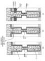
도 1a는 기판 상의 예시적인 막들의 개략적인 예시이다.
도 1b 내지 도 1j는 특정한 개시된 실시예들에 따른, 텅스텐 또는 몰리브덴이 증착될 수도 있는 다양한 구조체들의 개략적인 예들이다.
도 2a 내지 도 2c는 특정한 개시된 실시예들에 따른, 방법들에 대한 동작들을 도시하는 프로세스 흐름도이다.
도 3은 특정한 개시된 실시예들에 따른, 막들을 증착하기 위한 방법들의 예시적인 사이클들을 도시하는 타이밍 시퀀스도이다.
도 4a 내지 도 4j는 특정한 개시된 실시예들에 따른, 막들을 증착하기 위한 메커니즘의 일 예의 개략도들이다.
도 5는 H2/Ar/WClx/Ar 시퀀스 및 H2/Ar/n (WClx/Ar) 시퀀스를 사용하여 3-D NAND 구조체들의 텅스텐 충진을 비교하는 실험 결과들의 예시를 도시한다.
도 6은 특정한 개시된 실시예들을 수행하기 위한 예시적인 프로세스 툴의 개략도이다.
도 7은 특정한 개시된 실시예들을 수행하기 위한 예시적인 스테이션의 개략도이다.
도 8은 특정한 실시예들에 따라 사용될 수도 있는 매니폴드 시스템의 기본 피처들을 도시하는 개략도이다.
이하의 기술 (description) 에서, 제시된 실시예들의 완전한 이해를 제공하기 위해 수많은 구체적 상세들이 제시되었다. 개시된 실시예들은 이들 구체적인 상세들 중 일부 또는 전부가 없이 실시될 수도 있다. 다른 예들에서, 공지된 프로세스 동작들은 개시된 실시예들을 불필요하게 모호하게 하지 않기 위해 상세히 기술되지 않았다. 개시된 실시예들이 구체적인 실시예들과 함께 기술될 것이지만, 이는 개시된 실시예들을 제한하는 것으로 의도되지 않았다는 것이 이해될 것이다.
피처들의 텅스텐 (W) 충진은 전기적 콘택트들을 형성하기 위해 반도체 디바이스 제조에 자주 사용된다. 텅스텐 막들을 증착하는 종래의 방법들에서, 핵생성 텅스텐 층이 비아 또는 콘택트 내로 먼저 증착된다. 일반적으로, 핵생성 층은 그 위에 벌크 재료의 후속 형성을 용이하게 하도록 역할하는 박형의 컨포멀한 (conformal) 층이다. 텅스텐 핵생성 층은 피처의 측벽들 및 하단부를 컨포멀하게 코팅하도록 증착될 수도 있다. 아래에 놓인 피처 하단부 및 측벽들에 컨폼하는 (conform) 것은 고 품질 증착을 지지하는데 중요할 수 있다. 핵생성 층들은 종종 원자 층 증착 (atomic layer deposition; ALD) 또는 펄싱된 핵생성 층 (pulsed nucleation layer; PNL) 방법들을 사용하여 증착된다.
PNL 기법에서, 반응물질의 펄스들은 반응물질들 사이에 퍼지 가스의 펄스에 의해 반응 챔버로부터 순차적으로 주입되고 퍼지된다. 제 1 반응물질이 기판 상에 흡착될 수 있어, 다음 반응물질과 반응하는데 이용가능하다. 프로세스는 목표된 두께가 달성될 때까지 순환적 방식으로 반복된다. PNL 기법들은 ALD 기법들과 유사하다. PNL은 일반적으로 (1 Torr보다 큰) 보다 높은 동작 압력 범위 및 (사이클 당 1보다 큰 모노레이어 막 성장) 사이클 당 보다 높은 성장 레이트에 의해 ALD로부터 구별된다. PNL 증착 동안 챔버 압력은 약 1 Torr 내지 약 400 Torr의 범위일 수도 있다. 본 명세서에 제공된 기술 (description) 의 맥락에서, PNL은 반도체 기판 상의 반응을 위해 순차적으로 반응물질들을 부가하는 임의의 순환적 프로세스를 광범위하게 구현한다. 따라서, 이 개념은 종래에 ALD로 지칭된 기법들을 구현한다. 개시된 실시예들의 맥락에서, 화학적 기상 증착 (chemical vapor deposition; CVD) 은 반응물질들이 함께 증기-상 또는 표면 반응을 위해 반응기로 도입되는, 프로세스들을 구현한다. PNL 프로세스 및 ALD 프로세스는 CVD 프로세스들과 구별되고 그 반대도 된다.
텅스텐 핵생성 층이 증착된 후, 벌크 텅스텐은 통상적으로 수소 (H2) 와 같은 환원제를 사용하여 텅스텐 헥사플루오라이드 (WF6) 를 환원함으로써 CVD 프로세스에 의해 증착된다. 벌크 텅스텐은 텅스텐 핵생성 층과 상이하다. 본 명세서에서 사용된 바와 같은 벌크 텅스텐은 피처의 적어도 약 50 %와 같은 피처의 대부분 또는 전부를 충진하도록 사용된 텅스텐을 지칭한다. 그 위에 벌크 재료의 후속 형성을 용이하게 하도록 역할하는 박형의 컨포멀한 막인 핵생성 층과 달리, 벌크 텅스텐은 전류를 반송하도록 사용된다. 이는 핵생성 막과 비교하여 보다 큰 입자 크기 및 보다 낮은 저항률로 특징화될 수도 있다. 다양한 실시예들에서, 벌크 텅스텐은 적어도 50 Å의 두께로 증착된 텅스텐이다.
디바이스들이 보다 작은 기술 노드들로 스케일링되고 보다 복잡한 패터닝 구조체들이 사용되기 때문에, 텅스텐 충진에서 다양한 문제들이 있다. 종래의 텅스텐의 증착은 불소-함유 전구체 텅스텐 헥사플루오라이드 (WF6) 의 사용을 수반하였다. 그러나, WF6의 사용은 증착된 텅스텐 막 내로 불소의 어느 정도 통합을 발생시킨다. 불소의 존재는 인접한 컴포넌트들 내로 전자마이그레이션 (electromigration) 및/또는 불소 확산을 유발할 수 있고 콘택트들을 손상시킬 수 있어서, 디바이스의 성능을 저하시킨다. 일 과제는 증착된 텅스텐 막에서 불소 함량이 감소하는 것이다. 피처 사이즈가 감소됨에 따라 특정한 불소 농도의 효과는 상승한다. 이는 보다 박형의 막들이 보다 박형의 막들을 통해 확산하기 보다 쉬운 증착된 텅스텐 막의 불소와 함께 보다 작은 피처들 내에 증착되기 때문이다.
불소 확산을 방지하는 일 방법은 텅스텐으로부터 옥사이드 층과 같은 기판의 다른 층들로 불소가 확산하는 것을 방지하도록 텅스텐을 증착하기 전 하나 이상의 배리어 층들을 증착하는 단계를 포함한다. 예를 들어, 도 1a는 기판 상에 증착된 층들의 예시적인 스택을 도시한다. 기판 (190) 은 실리콘 층 (192), 옥사이드 층 (194) (예를 들어, 티타늄 옥사이드 (TiOx), 테트라에틸 오소실리케이트 (TEOS) 옥사이드, 등), 배리어 층 (196) (예를 들어, 티타늄 나이트라이드 (TiN)), 텅스텐 핵생성 층 (198), 및 벌크 텅스텐 층 (199) 을 포함한다. 배리어 층 (196) 은 벌크 텅스텐 층 (199) 및 텅스텐 핵생성 층 (198) 으로부터 옥사이드 층으로 불소 확산을 방지하도록 증착된다. 그러나, 디바이스들이 축소됨에 따라, 배리어 층들은 보다 박형이 되고, 불소는 여전히 증착된 텅스텐 층들로부터 확산할 수도 있다. 보다 고온에서 수행된 벌크 텅스텐의 화학적 기상 증착이 보다 낮은 불소 함량을 발생시키지만, 이러한 막들은 불량한 단차 커버리지 (step coverage) 를 가질 수도 있다.
또 다른 과제는 증착된 막들 상의 응력이 감소하는 것이다. 보다 박형의 텅스텐 막들은 상승된 인장 응력을 갖는 경향이 있다. CVD에 의해 벌크 텅스텐 막들을 증착하기 위한 종래의 기법들은 200 Å 막에 대해 2.5 GPa보다 큰 인장 응력을 갖는다. 고 열적 인장 응력은 기판으로 하여금 말리게 (curl) 하고, 이는 후속 프로세싱을 어렵게 한다. 예를 들어, 후속 프로세스들은 챔버에서 프로세스들을 수행하기 위해 화학적 기계적 평탄화, 재료들의 증착, 및/또는 기판 홀더로 기판의 클램핑을 포함할 수도 있다. 그러나, 이들 프로세스들은 종종 편평한 기판에 의존하고, 말린 기판은 불균일한 프로세싱 또는 기판 프로세싱 불능을 발생시킨다. 어닐링과 같이 다른 재료들의 막들의 응력을 감소시키기 위한 기존 방법들이 있지만, 텅스텐은 고 융점으로 인해 한번 증착되면 입자들로 하여금 이동되거나 변경되게 하는 표면 이동성을 갖지 않는다.
불소-프리 텅스텐 (FFW) 전구체들이 이러한 신뢰성 및 통합 문제들 또는 디바이스 성능 문제들을 방지하는데 유용하다. 현재 FFW 전구체들은 금속 유기 전구체들을 포함하지만, 금속 유기 전구체들로부터 탄소, 수소, 질소, 및 산소와 같은 원소들의 바람직하지 않은 추적들이 텅스텐 막에도 통합될 수도 있다. 일부 금속 유기 불소-프리 전구체들은 또한 텅스텐 증착 프로세스들로 용이하게 구현 또는 통합되지 않는다.
본 명세서에 기술된 일부 구현예들은 텅스텐 클로라이드 (WClx) 전구체를 사용한 텅스텐의 증착과 관련한다. 텅스텐 클로라이드는 텅스텐 펜타클로라이드 (WCl5), 텅스텐 헥사클로라이드 (WCl6), 텅스텐 테트라클로라이드 (WCl4), 텅스텐 디클로라이드 (WCl2), 및 이들의 혼합물들을 포함한다. 본 명세서의 예들이 예들로서 WCl5 및 WCl6를 참조하지만, 다른 텅스텐 클로라이드들이 개시된 실시예들과 함께 사용될 수도 있다는 것이 이해된다. 특정한 개시된 실시예들을 사용하여 증착된 막들은 불소-프리이다. 특정한 개시된 실시예들은 염소-함유 텅스텐 전구체 및 수소의 교번하는 펄스들을 사용하여 벌크 텅스텐을 증착하는 것으로 지향된다.
WCl5 및 WCl6에 의한 증착은 텅스텐 클로라이드들에 의해 가능한 에칭으로 인해 WF6와 함께 존재하지 않는 과제들을 제공한다. 텅스텐 클로라이드들은 보다 적은 반응성이고, 그 결과, 증착은 WF6를 사용한 증착보다 높은 온도에서 수행된다. 증발된 WCl6는 텅스텐 증착 챔버 내로 반송하는 것을 인에이블하도록 충분히 높은 증기압을 갖는다. 그러나, WCl6 는 WCl5보다 기판을 에칭할 가능성이 높을 수도 있다. WCl5가 기판을 에칭할 가능성이 보다 낮지만, WCl5는 또한 WCl6보다 높은 증기압을 갖는다. 보다 낮은 증기압이 저 저항률을 갖는 텅스텐 막들을 증착하는데 유용하지만, 일부 증착 동작들은 불량한 단차 커버리지를 가질 수도 있다.
본 명세서에 기술된 방법들은 몰리브덴 클로라이드 또는 몰리브덴 옥시클로라이드 전구체들에 의한 몰리브덴 (Mo) 의 증착을 위해 또한 사용될 수도 있다. 몰리브덴은 저 저항 금속화 스택 구조체들을 형성하도록 사용될 수도 있고 텅스텐의 자리를 취할 수도 있다.
개시된 실시예들은 광범위한 다양한 적용예들을 갖는다. 방법들은 고 단차 커버리지를 갖는 피처들 내로 텅스텐 또는 몰리브덴을 증착하도록 사용될 수도 있고, 3D NAND 구조체들 내로 텅스텐을 증착하도록 또한 사용될 수도 있다.
본 명세서에 기술된 방법들은 챔버에 하우징될 수도 있는 기판 상에서 수행된다. 기판은 유전체, 도전 또는 반도전 재료와 같은 재료의 하나 이상의 층들이 그 위에 증착된 웨이퍼들을 포함하는, 실리콘 또는 다른 반도체 웨이퍼, 예를 들어, 200-㎜ 웨이퍼, 300-㎜ 웨이퍼, 또는 450-㎜ 웨이퍼일 수도 있다. 방법들은 반도체 기판들로 제한되지 않고, 텅스텐과 같은 금속으로 임의의 피처를 충진하도록 수행될 수도 있다.
기판들은 좁은 그리고/또는 재차 들어간 (re-entrant) 개구부들, 피처 내 협폭부들 (constrictions), 및 고 종횡비들 중 하나 이상을 특징으로 할 수도 있는, 비아 또는 콘택트 홀들과 같은 피처들을 가질 수도 있다. 피처가 상기 기술된 층들 중 하나 이상에 형성될 수도 있다. 예를 들어, 피처는 유전체 층에 적어도 부분적으로 형성될 수도 있다. 일부 실시예들에서, 피처는 적어도 약 2:1, 적어도 약 4:1, 적어도 약 6:1, 적어도 약 10:1, 적어도 약 25:1, 이상의 종횡비를 가질 수도 있다. 피처의 일 예는 반도체 기판 또는 기판 상의 층 내의 홀 또는 비아이다.
도 1b 내지 도 1h는 개시된 실시예들에 따른, 금속이 증착될 수도 있는 다양한 구조체들의 개략적인 예들이다. 도 1b는 텅스텐 또는 몰리브덴과 같은 금속으로 충진될 수직 피처 (101) 의 단면도의 일 예를 도시한다. 피처는 기판 (103) 내에 피처 홀 (105) 을 포함할 수 있다. 홀 (105) 또는 다른 피처는 개구부 근방 치수, 예를 들어, 약 10 ㎚ 내지 500 ㎚, 예를 들어 약 25 ㎚ 내지 약 300 ㎚의 개구부 직경 또는 라인 폭을 가질 수도 있다. 피처 홀 (105) 은 충진되지 않은 피처 또는 단순히 피처로 지칭될 수 있다. 피처 (101), 및 임의의 피처가 수직 축들을 갖는 수직으로 배향된 피처들 및 수평 축들을 갖는 수평으로 배향된 피처들을 갖는 피처의 길이를 통해 연장하는 축 (118) 에 의해 부분적으로 특징화될 수도 있다.
일부 실시예들에서, 피처들은 3D NAND 구조체의 워드라인 피처들이다. 예를 들어, 기판이 적어도 200 Å 깊이의 수직 채널들을 갖는 임의의 수의 워드라인들 (예를 들어, 50 내지 150) 을 갖는 워드라인 구조체를 포함할 수도 있다. 또 다른 예는 기판 또는 층의 트렌치이다. 피처들은 임의의 깊이일 수도 있다. 다양한 실시예들에서, 피처는 배리어 층 또는 접착 층과 같은, 하부 층을 가질 수도 있다. 하부 층들의 비제한적인 예들은 유전체 층들 및 도전 층들, 예를 들어, 실리콘 옥사이드들, 실리콘 나이트라이드들, 실리콘 카바이드들, 금속 옥사이드들, 금속 나이트라이드들, 금속 카바이드들, 및 금속 층들을 포함한다.
도 1c는 재차 들어간 프로파일을 갖는 피처 (101) 의 일 예를 도시한다. 재차 들어간 프로파일은 피처의 하단부, 폐쇄된 단부, 또는 내부로부터 피처 개구부로 좁아지는 프로파일이다. 다양한 구현예들에 따라, 프로파일은 점진적으로 좁아질 수도 있고 그리고/또는 피처 개구부에서 오버행 (overhang) 을 포함할 수도 있다. 도 1c는 피처 홀 (105) 의 측벽 또는 내부 표면들을 라이닝하는 하부 층 (113) 을 갖는, 후자의 예를 도시한다. 하부 층 (113) 은 예를 들어, 확산 배리어 층, 접착 층, 핵생성 층, 이의 조합, 또는 임의의 다른 적용가능한 재료일 수 있다. 하부 층들의 비제한적인 예들은 유전체 층들 및 도전 층들, 예를 들어, 실리콘 옥사이드들, 실리콘 나이트라이드들, 실리콘 카바이드들, 금속 옥사이드들, 금속 나이트라이드들, 금속 카바이드들, 및 금속 층들을 포함할 수 있다. 특정한 구현예들에서 하부 층은 티타늄, 티타늄 나이트라이드, 텅스텐 나이트라이드, 티타늄 알루미나이드, 텅스텐, 및 몰리브덴 중 하나 이상일 수 있다. 일부 실시예들에서, 하부 층은 텅스텐-프리이다. 일부 실시예들에서, 하부 층은 몰리브덴-프리이다. 하부 층 (113) 은 하부 층 (113) 이 피처 (101) 내부보다 피처 (101) 의 개구부에서 보다 두껍도록 오버행 (115) 을 형성한다.
일부 구현예들에서, 피처 내부에 하나 이상의 협폭부들을 갖는 피처들이 충진될 수도 있다. 도 1d는 협폭부들을 갖는 다양한 충진된 피처들의 도면들의 예들을 도시한다. 도 1d의 예들 (a), (b) 및 (c) 각각은 피처 내 중간지점에 협폭부들 (109) 을 포함한다. 협폭부들 (109) 은 예를 들어, 약 15 ㎚ 내지 20 ㎚ 넓이일 수 있다. 협폭부들은 종래의 기법들을 사용하여 피처 내 텅스텐 또는 몰리브덴의 증착 동안 핀치 오프 (pinch off) 를 유발할 수 있고, 추가 증착을 차단하는 증착된 금속이 피처의 일부가 충진되기 전 협폭부를 넘어가 (past), 피처 내 보이드들을 발생시킨다. 예 (b) 는 피처 개구부에서 라이너/배리어 오버행 (115) 을 더 포함한다. 이러한 오버행은 잠재적인 핀치 오프 지점일 수 있다. 예 (c) 는 예 (b) 의 오버행 (115) 보다 필드 영역으로부터 더 먼 협폭부 (112) 를 포함한다.
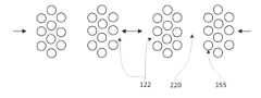
3-D 메모리 구조체들 내와 같이, 수평 피처들이 또한 충진될 수 있다. 도 1e는 협폭부 (151) 를 포함하는 수평 피처 (150) 의 일 예를 도시한다. 예를 들어, 수평 피처 (150) 는 3D NAND 구조체의 워드라인일 수도 있다. 일부 구현예들에서, 협폭부들은 3D NAND 또는 다른 구조체의 필라들 (pillars) 의 존재로 인한 것일 수 있다. 예를 들어, 도 1f는 VNAND 스택들 (좌측 (125) 및 우측 (126)), 중앙 수직 구조체 (130), 및 중앙 수직 구조체 (130) 의 마주보는 측벽들 (140) 상의 개구부들 (122) 을 갖는 복수의 스택된 수평 피처들 (120) 을 갖는 3-D NAND (또한 수직 NAND 또는 VNAND로 지칭됨) 구조체 (110) (반도체 기판 (103) 상에 형성된) 의 측단면도를 제공한다. 도 1f는 함께 "트렌치-유사 (trench-like)" 중앙 수직 구조체 (130) 를 형성하는 표현된 3-D NAND 구조체 (110) 의 2 개의 "스택들"을 디스플레이하지만, 특정한 실시예들에서, 차례로 배치되고 서로 공간적으로 평행하게 진행하는 3 개 이상의 "스택들"이, 도 1f에 명시적으로 예시된 것과 같은, 중앙 수직 구조체 (130) 를 형성하는 인접한 "스택들"의 쌍 각각 사이의 갭이 있을 수도 있다는 것을 주의하라. 이 실시예에서, 수평 피처들 (120) 은 개구부들 (122) 을 통해 중앙 수직 구조체 (130) 로부터 유체적으로 액세스가능한 3-D 메모리 워드라인 피처들이다. 도면에 명시적으로 나타나지 않지만, 도 1f에 도시된 3-D NAND 스택들 (125 및 126) 모두 (즉, 좌측 3-D NAND 스택 (125) 및 우측 3-D NAND 스택 (126)) 에 존재하는 수평 피처들 (120) 은 또한 스택들 (각각 극좌측 및 극우측) 의 다른 측면들로부터 부가적인 3-D NAND 스택들 (극좌측 및 극우측으로, 미도시) 에 의해 형성된 유사한 수직 구조체들을 통해 액세스가능하다. 달리 말하면, 3-D NAND 스택 (125, 126) 각각은 중앙 수직 구조체 (130) 를 통해 3-D NAND 스택의 양 측면들로부터 유체적으로 액세스가능한 워드라인 피처들의 스택을 포함한다. 도 1f에 개략적으로 예시된 특정한 예에서, 3-D NAND 스택 각각은 6 쌍의 스택된 워드라인들을 포함하지만, 다른 실시예들에서, 3-D NAND 메모리 레이아웃은 임의의 수의 수직으로 스택된 쌍들의 워드라인들을 포함할 수도 있다.
3-D NAND 스택의 워드라인 피처들은 통상적으로 실리콘 옥사이드 층 및 실리콘 나이트라이드 층의 교번하는 스택을 증착하고, 이어서 사이에 갭들을 갖는 옥사이드들 층들의 스택을 남기면서 나이트라이드 층들을 선택적으로 제거함으로써 형성된다. 이들 갭들은 워드라인 피처들이다. 임의의 수의 워드라인들이 이들을 형성하는데 이용가능한 기법, 뿐만 아니라 수직 피처들의 (실질적으로) 보이드-프리 충진들을 성공적으로 달성하도록 이용가능한 기법이 있는 한, 이러한 3-D NAND 구조체에 수직으로 스택될 수도 있다. 따라서, 예를 들어, VNAND 스택이 2 내지 256 개의 수평 워드라인 피처들, 또는 8 내지 128 개의 수평 워드라인 피처들, 또는 16 내지 64 개의 수평 워드라인 피처들, 등을 포함할 수도 있다 (열거된 범위들은 언급된 엔드포인트들을 포함하는 것으로 이해됨).
도 1g는 도 1f의 측면에 도시된 동일한 3-D NAND 구조체 (110) 의 단면 톱-다운 (top-down) 도를 도 1f의 점선 수평 라인으로 나타낸 바와 같은 수평 섹션 (160) 을 통해 취해진 단면과 함께 제공한다. 도 1g의 단면도는 반도체 기판 (103) 의 베이스 (base) 로부터 3-D NAND 스택 (110) 의 상단부로 수직으로 진행하는 것으로 도 1f에 도시된 몇몇 행들의 필라들 (155) 을 예시한다. 일부 실시예들에서, 이들 필라들 (155) 은 폴리실리콘 재료로부터 형성되고 3-D NAND 구조체 (110) 에 구조적으로 그리고 기능적으로 중요하다. 일부 실시예들에서, 이러한 폴리실리콘 필라들이 필라들 내에 형성된 스택된 메모리 셀들에 대해 게이트 전극들로서 역할을 할 수도 있다. 도 1g의 상면도는 필라들 (155) 이 워드라인 피처들 (120) 로 개구부들 (122) 내에 협폭부들을 형성한다는 것을 예시한다 - 즉 중앙 수직 구조체 (130) 로부터 개구부들 (122) (도 1g의 화살표들로 나타낸 바와 같이) 을 통한 워드라인 피처들 (120) 의 유체 액세스가능성이 필라들 (155) 에 의해 억제된다. 일부 실시예들에서, 인접한 폴리실리콘 필라들 사이의 수평 갭의 사이즈는 약 1 내지 20 ㎚이다. 이 유체 액세스가능성의 감소는 텅스텐 재료로 워드라인 피처들 (120) 을 균일하게 충진하는 것의 어려움을 증가시킨다. 워드라인 피처들 (1) 의 구조체 및 필라들 (155) 의 존재로 인한 텅스텐 재료 또는 몰리브덴 재료로 이들을 균일하게 충진하는 것의 어려움은 도 1h, 도 1i 및 도 1j에 더 예시된다.
도 1h는 도 1f에 도시된 것과 유사하지만, 이 도면에서는 단일 쌍의 워드라인 피처들 (120) 에 포커싱하고, 부가적으로 충진된 워드라인 피처들 (120) 의 보이드 (175) 의 형성을 발생시키는, 금속 충진 프로세스를 개략적으로 예시하는, 수직으로 절단된 (cut through) 3-D NAND 구조체를 나타낸다. 도 1i는 또한 보이드 (175) 를 개략적으로 예시하지만, 이 도면에서 도 1g에 나타낸 수평 절단도와 유사한, 수평 절단 필라들 (155) 을 통해 예시된다. 도 1j는 협폭부 형성 필라들 (155) 주변에 텅스텐 또는 몰리브덴 재료의 축적을 예시하고, 축적은 부가적인 텅스텐 또는 몰리브덴 재료가 보이드들 (175) 의 영역 내에 증착될 수 없도록 개구부들 (122) 의 핀치 오프를 발생시킨다. 보이드-프리 텅스텐 또는 몰리브덴 충진이 개구부들 (122) 의 핀치 오프를 유발하고 워드라인 피처들 (120) 내로 추가 전구체 마이그레이션을 방지하는, 필라들 (155) 주변 텅스텐의 축적된 증착 전에, 수직 구조체 (130) 를 통해, 개구부들 (122) 을 통해, 협폭 필라들 (155) 을 넘어, 워드라인 피처들 (120) 의 가장 먼 범위까지 아래로 충분한 양의 증착 전구체의 마이그레이션에 의존한다는 것이 도 1h 및 도 1i로부터 자명하다. 유사하게, 도 1j는 위에서 단면으로 본 단일 워드라인 피처 (120) 를 나타내고, 상당한 폭의 필라들 (155) 이 그렇지 않으면 워드라인 피처 (120) 를 통한 개방 경로일 수 있는 워드라인 피처 (120) 를 부분적으로 차단, 그리고/또는 좁히고 (narrow), 그리고/또는 협폭화하도록 작용한다는 사실로 인해, 대체로 컨포멀한 텅스텐 또는 몰리브덴 재료의 증착이 워드라인 피처 (120) 의 내부를 핀치 오프하기 시작하는 지 예시한다. (도 1j의 예는 도 1i에 도시된 필라 협폭부들의 구조체의 3-D 피처들의 2-D 렌더링으로 이해될 수 있어서, 단면도가 아니라 평면도에서 볼 수 있는 협폭부들을 예시한다는 것이 이해되어야 한다.)
3D 구조체들이 최내측 영역 및 최하측 영역으로 하여금 충진되게 하도록 전구체들로 보다 길고 그리고/또는 보다 집중된 노출을 필요로 할 수도 있다. 3D 구조체들은 WClx 전구체들을 채용할 때 구조체의 부분들로서 보다 많은 에칭을 허용하는 보다 길고 보다 집중된 노출과 함께, 이들의 에칭 성향으로 인해, 특히 어려울 수 있다. 이들 과제들은 또한 몰리브덴 클로라이드 전구체들을 사용해도 존재할 수도 있다.
수평으로 배향된 및 수직으로 배향된 피처들에 대한 피처 충진의 예들은 이하에 기술된다. 대부분의 경우, 이 예들은 수평으로 배향된 또는 수직으로 배향된 피처들 모두에 적용가능하다는 것을 주의해야 한다. 게다가, 이하의 기술에서, 용어 "측방향 (lateral)"은 피처 축에 일반적으로 직교하는 방향을 지칭하고 용어 "수직 (vertical)"은 일반적으로 피처 축을 따른 방향을 지칭하도록 사용될 수도 있다는 것을 또한 주의해야 한다.
다양한 실시예들에 따라, 이하에 기술된 방법들은 ALD 사이클의 복수의 환원제/퍼지 사이클들 및/또는 복수의 금속-전구체/퍼지 사이클들에 구조체를 노출하는 것을 수반한다. 일부 구현예들에서, 다음의 장점들 중 하나 이상이 달성될 수도 있다. 일부 실시예들에서, 퍼지 가스 펄싱과 함께 배치된 복수의 텅스텐-함유 전구체 도즈들 (예를 들어, W/Ar/W/Ar/W/Ar/W/Ar, W는 텅스텐-함유 전구체의 펄스이고 Ar은 아르곤 퍼지 가스의 펄스를 나타냄) 은 3-D NAND 워드라인 구조체 내로 깊이 텅스텐-함유 전구체의 전달을 인에이블하거나 구조체로 충진하는 것을 어렵게 한다. 일부 구현예들에서, 다음의 장점들 중 하나 이상이 달성될 수도 있다. 일부 실시예들에서, 퍼지 가스 펄싱과 함께 배치된 복수의 몰리브덴-함유 전구체 도즈들 (예를 들어, Mo/Ar/Mo/Ar/Mo/Ar/Mo/Ar, Mo는 몰리브덴-함유 전구체의 펄스이고 Ar은 아르곤 퍼지 가스의 펄스를 나타냄) 은 3-D NAND 워드라인 구조체 내로 깊이 몰리브덴-함유 전구체의 전달을 인에이블하거나 구조체로 충진하는 것을 어렵게한다.
금속-함유 펄스 각각 후 불활성 가스 퍼지 펄스는 금속-함유 전구체의 모노레이어가 구조체 전반에 흡착된다는 것을 보장할 수 있다. 일부 실시예들에서, 각각 퍼지 가스가 이어지는, 복수의 펄스들은 금속-함유 전구체의 복수의 모노레이어들이 보다 액세스가능한 구조체의 부분들에서 축적 (build up) 되지 않는다는 것을 보장한다. 이는 구조체의 원치 않은 에칭을 방지할 수 있다. 일부 실시예들에서, 교번하는 펄스들을 갖는 것은 펄스 각각 전에 금속 전구체 저장부의 가압을 인에이블한다. 이는 피처의 하단부로의 플럭스를 보조할 수 있다. 일부 실시예들에서, 퍼지 가스 펄스들 펄싱과 함께 배치된 복수의 환원제 도즈들 (예를 들어, H2/Ar/H2/Ar/W/Ar/W/Ar, 여기서 H2는 환원제이고, W는 텅스텐-함유 전구체의 펄스 그리고 Ar은 아르곤 퍼지 가스의 펄스이고 또는 H2/Ar/H2/Ar/Mo/Ar/Mo/Ar 여기서 Mo는 몰리브덴-함유 전구체의 펄스를 나타냄) 은 흡착된 클로라이드들과 반응하도록 환원제에 충분한 시간을 제공하는 한편, 반응 생성물 (예를 들어, HCl) 로 하여금 표면을 떠나고 다음 펄스의 환원제를 위한 공간을 만들게 한다.
이하의 기술은 텅스텐 피처 충진 및 몰리브덴 피처 충진에 포커싱하지만, 본 개시의 양태들은 다른 재료들로 피처들을 충진시 또한 구현될 수도 있다. 예를 들어, 본 명세서에 기술된 하나 이상의 기법들을 사용한 피처 충진은 다른 텅스텐 함유 재료들 (예를 들어, 텅스텐 나이트라이드 (WN) 및 텅스텐 카바이드 (WC)), 티타늄 함유 재료들 (예를 들어, 티타늄 (Ti), 티타늄 나이트라이드 (TiN), 티타늄 실리사이드 (TiSi), 티타늄 카바이드 (TiC) 및 티타늄 알루미나이드 (TiAl)), 탄탈룸 함유 재료들 (예를 들어, 탄탈룸 (Ta), 및 탄탈룸 나이트라이드 (TaN)), 및 니켈 함유 재료들 (예를 들어, 니켈 (Ni) 및 니켈 실리사이드 (NiSi)) 을 포함하는 다른 재료들로 피처들을 충진하도록 사용될 수도 있다. 또한, 본 명세서에 개시된 방법들 및 장치는 피처 충진으로 제한되지 않고, 평면형 표면들 상에 블랭킷 (blanket) 막들을 형성하는 것을 포함하여 임의의 적절한 표면 상에 텅스텐을 증착하도록 사용될 수 있다.
도 2a 내지 도 2c는 개시된 실시예들에 따라 수행된 방법들에 대한 프로세스 흐름도들을 제공한다. 이하에 기술된 바와 같이, 방법은 텅스텐으로 기판 상의 구조체를 충진하도록 수행된다. 구조체들의 예들은 도 1b 내지 도 1h를 참조하여 상기 기술되었다.
온도는 채용된 화학물질에 따라 가변할 수도 있다. WClx 및 WOxCl4 전구체들에 대해, 특정한 개시된 실시예들은 약 400 ℃ 내지 약 600 ℃, 예컨대 약 525 ℃의 기판 온도에서 수행될 수도 있다. 기판 온도는 기판을 홀딩하는 페데스탈이 설정되는 온도를 지칭한다.
MoClx 및 MoOxCly 전구체들에 대해, 특정한 개시된 실시예들은 약 400 ℃ 내지 약 600 ℃, 예컨대 약 525 ℃의 기판 온도에서 수행될 수도 있다. 기판 온도는 기판을 홀딩하는 페데스탈이 설정되는 온도를 지칭한다.
특정한 개시된 실시예들은 약 3 Torr 내지 약 60 Torr의 챔버 압력에서 수행될 수도 있다. 일부 실시예들에서, WClx 전구체들을 사용한 텅스텐 증착을 위한 챔버 압력은 5 Torr 내지 20 Torr, 예를 들어, 10 Torr이다.
도 2a를 참조하면, 동작 200에서, 텅스텐 또는 몰리브덴으로 충진될 구조체가 환원제 펄스에 노출된다. 일부 실시예들에서, 환원제 펄스는 수소 (H2) 이다. 실란들, 보란들, 게르만들, 포스핀들, 수소-함유 가스들, 및 이들의 조합들을 포함하는, 다른 환원제들이 사용될 수도 있다. 다양한 실시예들에서, 벌크 텅스텐 증착 또는 벌크 몰리브덴 증착이 환원제로서 수소를 사용하여 수행된다. 환원제는 또 다른 반응물질을 흘리지 않고 펄싱된다. 일부 실시예들에서, 캐리어 가스가 흐를 수도 있다. 일부 실시예들에서, 캐리어 가스, 예컨대 질소 (N2), 아르곤 (Ar), 헬륨 (He), 또는 다른 불활성 가스들이 동작 200 동안 흐를 수도 있다.
동작 200은 임의의 적합한 지속기간 동안 수행될 수도 있다. 예시적인 지속기간들은 약 0.25 초 내지 약 30 초, 약 0.25 초 내지 약 20 초, 약 0.25 초 내지 약 5 초, 또는 약 0.5 초 내지 약 3 초를 포함한다.
동작 202에서, 챔버는 기판의 표면에 흡착되지 않은 과잉 수소를 제거하도록 퍼지된다. 퍼지가 고정된 압력으로 불활성 가스를 흘리고, 이에 따라 챔버의 압력을 감소시키고 또 다른 반응물질 가스 노출을 개시하기 전 챔버를 재-가압함으로써 수행될 수도 있다. 예시적인 불활성 가스들은 질소 (N2), 아르곤 (Ar), 헬륨 (He), 및 이들의 혼합물들을 포함한다. 퍼지는 약 0.25 초 내지 약 30 초, 약 0.25 초 내지 약 20 초, 약 0.25 초 내지 약 5 초, 또는 약 0.5 초 내지 약 3 초의 지속기간 동안 수행될 수도 있다.
동작 200 및 동작 202는 이어서k 회 수행될 때까지 반복되고, 여기서k는 적어도 21의 정수이다. 일 예에서, 동작 200은 0.5 초의 지속기간, 그리고 동작 202는 환원제 펄스들 사이에 1 초의 지속기간을 가질 수도 있다.k= 10에 대해, 1 × 10 = 10 초의 총 퍼지 시간과 함께, 총 텅스텐 전구체 시간은 0.5 × 10 = 5 초이다.
동작 204에서, 기판은 텅스텐 전구체에 또는 몰리브덴 전구체에 노출된다. 예시적인 전구체들은 텅스텐 클로라이드들 및 텅스텐 옥시클로라이드들과 같은 염소-함유 텅스텐 전구체들을 포함한다. 텅스텐 클로라이드들은 WClx일 수도 있고, 여기서 x는 2 이상 6 이하의 정수, 예컨대 2, 3, 4, 5, 또는 6이다. 예들은 WCl5 및 WCl6를 포함한다. 염소-함유 텅스텐 전구체는 WClx 화합물들의 혼합물을 포함할 수도 있다. 텅스텐 옥시클로라이드들은 WOxCly를 포함하고, x 및 y는 0보다 큰 수이다. 몰리브덴 클로라이드들 및 몰리브덴 옥시클로라이드들을 포함하는 몰리브덴 전구체들은 몰리브덴을 증착하도록 사용된다. 이들은 몰리브덴 펜타클로라이드 (MoCl5), 몰리브덴 디클로라이드 다이옥사이드 (MoO2Cl2), 몰리브덴 테트라클로라이드 옥사이드 (MoOCl4) 를 포함한다.
일부 실시예들에서, 캐리어 가스, 예컨대 질소 (N2), 아르곤 (Ar), 헬륨 (He), 또는 다른 불활성 가스들이 동작 206 동안 흐를 수도 있다.
동작 204는 임의의 적합한 지속기간 동안 그리고 임의의 적합한 온도로 수행될 수도 있다. 일부 예들에서, 동작 206은 약 0.25 초 내지 약 30 초, 약 0.25 초 내지 약 20 초, 약 0.25 초 내지 약 5 초, 또는 약 0.5 초 내지 약 3 초의 지속기간 동안 수행될 수도 있다. 이 동작은 일부 실시예들에서 기판의 표면 상의 활성 사이트들 (active sites) 을 포화시키기 충분한 지속기간 동안 수행될 수도 있다. 일부 실시예들에서, 전구체는 가스 라인을 충진하고 도징 전 라인 변화를 위해 방향전환 (divert) 될 수도 있다. 캐리어 가스는 동작 202에 대해 상기 기술된 것들 중 임의의 가스일 수도 있다.
다양한 실시예들에 따라, 동작 204 동안, 일부 WClx는 동작 200으로부터 표면 상에 남아 있는 H2와 반응할 수도 있고 일부 WClx는 표면 상에 남아 있는 H2와 완전히 반응하지 않을 수도 있다. 또한 다양한 실시예들에서, 일부 H2는 WClx와 전혀 반응하지 않을 수도 있고 WClx는 대신 H2가 기판 표면 상에 물리흡착 또는 남지 않는, 기판의 표면 상에 물리흡착될 수도 있다. 일부 실시예들에서, H2는 기판 표면 상에 남아 있을 수도 있지만 표면 상에 물리흡착 또는 화학흡착하지 않을 수도 있다. 도 2a의 동작 204는 이에 따라 일부 실시예들에서 텅스텐의 반-모노레이어 (sub-monolayer) 를 형성할 수도 있다. 유사하게, 동작 204는 일부 실시예들에서 몰리브덴의 반-모노레이어를 형성할 수도 있다.
동작 206에서, 피처의 표면 상의 수소 또는 다른 환원제와 반응하지 않은 여전히 가스 상인 과도한 전구체를 퍼지가 퍼지하도록 수행된다. 퍼지가 고정된 압력으로 불활성 가스를 흘리고, 이에 따라 챔버의 압력을 감소시키고 또 다른 가스 노출을 개시하기 전 챔버를 재-가압함으로써 수행될 수도 있다.
챔버는 임의의 적합한 지속기간 동안 퍼지될 수도 있다. 챔버는 약 0.25 초 내지 약 30 초, 약 0.25 초 내지 약 20 초, 약 0.25 초 내지 약 5 초, 또는 약 0.5 초 내지 약 3 초의 지속기간 동안 퍼지될 수도 있다. 일부 실시예들에서, 퍼지 지속기간은 약 0.1 초 내지 약 2 초이고 텅스텐의 표면으로 WClx의 저 흡착 레이트로 인해 기판 표면으로부터 WClx 또는 다른 전구체 모두를 제거하는 것을 방지할 수도 있다. 일부 실시예들에서, 퍼지 지속기간은 약 0.1 초 내지 약 15 초, 예컨대 약 7 초이다. 예를 들어, 3D NAND 구조체의 제조 동안, 챔버는 동작 206 동안 약 2 초 동안 퍼지될 수도 있다. 퍼지 가스는 동작 202에 대해 상기 기술된 가스들 중 임의의 가스일 수도 있다.
동작 204 및 동작 206은 이어서n 회 수행될 때까지 반복되고, 여기서k는 적어도 2의 정수이다. 이하에 더 기술된 바와 같이, 증착 시퀀스에서 퍼지들에 의해 분리된 복수의 텅스텐 펄스들을 수행함으로써, 원치 않은 에칭이 구조체들의 상단부들 및 에지들에서 감소될 수도 있다. 일 예에서, 동작 204는 0.7 초의 지속기간, 그리고 동작 206은 텅스텐 전구체 펄스들 사이에 2 초의 지속기간을 가질 수도 있다.n= 10에 대해, 2 × 10 = 20 초의 총 퍼지 시간과 함께, 총 텅스텐 전구체 시간은 0.7 × 10 = 7 초이다.
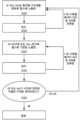
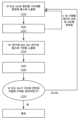
동작 208에서, 텅스텐 또는 몰리브덴 층이 적절한 두께로 증착되었는지 여부가 결정된다. 그렇지 않으면, 동작 200 내지 동작 206은 텅스텐 또는 몰리브덴 층의 목표된 두께는 피처의 표면 상에 증착될 때까지 반복된다. 동작 200 내지 동작 206의 반복 각각은 "사이클"로 지칭될 수도 있다. 일부 실시예들에서, 동작들 200/202 및 동작들 204/206의 순서는 텅스텐 또는 몰리브덴 전구체가 환원제의 도입 전에 도입되도록 반전될 수도 있다.
도 2b는 동작 200 및 동작 202가 사이클 동안 반복되지 않도록 ALD 사이클 각각이 단일 환원제 펄스 및 복수의 텅스텐 또는 몰리브덴 전구체 펄스들을 포함하는 실시예들에 대한 프로세스 흐름도를 제공한다. 도 2c는 동작 204 및 동작 206이 사이클 동안 반복되지 않도록 ALD 사이클 각각이 단일 텅스텐 또는 몰리브덴 전구체 펄스 및 복수의 환원제 펄스들을 포함하는 실시예들에 대한 프로세스 흐름도를 제공한다. 도 2b 및 도 2c의 프로세스 블록들은 그 외에는 도 2a에 대해 상기 기술된 바와 같다.
도 3은 H2 및 WClx를 사용하여 텅스텐을 증착하기 위한 프로세스에서 예시적인 증착 사이클들 311A 및 311B를 도시하는 타이밍 시퀀스도를 제공한다. 도 3은 도 2a 내지 도 2c의 동작 200의 일 실시예의 일 예인, 증착 사이클 311A에서의 H2펄스를 도시한다. 도 3의 예에서, H2펄스 동안, Ar 및 WClx 플로우들은 턴오프된다. 다른 실시예들에서, 퍼지 가스가 환원제 펄스 동안 계속해서 흐를 수도 있다. 일부 실시예들에서, 환원제 펄스 동안 퍼지 가스를 턴오프하는 것은 환원제로의 노출을 증가시키는데 유리하다. H2 직후, Ar 펄스가 도시된다. 이는 도 2a 내지 도 2c의 동작 202의 일 실시예의 일 예이다. 퍼지 펄스 동안, H2 및 WClx 플로우들은 턴오프된다. 320에서, 점선 박스는 이어서 텅스텐 전구체 펄스를 개입시키지 않고 수행되는, 임의의 수의 H2/Ar 퍼지 펄스들을 나타낸다. 이는 도 2a 및 도 2c의 동작 200 및 동작 202의 일 실시예의 일 예이다. 5 개의 H2/Ar 펄스 시퀀스들이 도시되지만, H2/Ar 펄스 시퀀스들의 수는 상기 기술된 바와 같이 1 내지k의 범위일 수 있다. 340에서 점선 박스는 환원제 펄스를 개입시키지 않고 수행되는 반복된 WClx/Ar 퍼지 펄스들을 나타낸다. 이는 도 2a 및 도 2b의 동작 204 및 동작 206의 일 실시예의 일 예이다. WClx 펄스 동안, Ar 밸브는 폐쇄되고 Ar 펄스 동안, WClx 밸브는 폐쇄된다. 수소 플로우는 프로세스 전반에 오프된다. 4 개의 WClx/Ar 펄스 시퀀스들이 도시되지만, WClx/Ar 펄스 시퀀스들의 수는 상기 기술된 바와 같이 1 내지n의 범위일 수 있다.
일부 실시예들에서, Ar 플로우는 H2 및/또는 WClx 펄스들 동안 온으로 남아 있을 수도 있고, Ar 펄스들은 H2 및 WClx 플로우들 없이, 일부 실시예들에서, 증가된 Ar 플로우를 특징으로 한다는 것을 주의해야 한다. 그러나, 텅스텐 전구체 펄스 동안 (희석되어 전달될 수도 있는) 텅스텐 전구체 가스의 희석을 더 방지하기 위해 퍼지 가스를 턴오프하는 것이 유리할 수 있다. 3-D NAND 구조체들의 충진은 웨이퍼에서 보다 높은 W 농도로부터 유리하고; 희석은 불량한 충진을 발생시킬 것이다. 게다가, 텅스텐 전구체 펄스 동안 퍼지 가스를 턴오프하고 퍼지 매니폴드를 가압하는 것은 그 사이에 W 펄스들을 갖는 연속적인 퍼지 플로우보다 효율적인 챔버의 퍼지를 인에이블한다. 유사하게, 이는 환원제 가스의 희석을 방지하기 위해 환원제 펄스 동안 퍼지 가스를 턴오프하는데 유리할 수도 있다. 도 3에 도시된 바와 같이, Ar 펄스는 증착 사이클 311A를 종료한다.
WClx가 도 3의 예에서 예시적 목적들로 도시되었지만, 도 3의 타이밍 시퀀스는 텅스텐 옥시클로라이드 전구체들 및 몰리브덴 클로라이드 및 몰리브덴 옥시클로라이드 전구체들을 포함하는 다른 전구체들에 대해 사용될 수도 있다. 유사하게, 다른 퍼지 가스들 및/또는 다른 환원제들이 Ar 및 H2 대신 사용될 수도 있다.
도 2a 내지 도 2c에 기술된 프로세스들 및 도 3을 참조하여 기술된 펄스 시퀀스는 펄스 시퀀스의 일 예이다. 당업자는 이루어질 수도 있는 다양한 수정들이 있다는 것을 이해할 것이다. 예를 들어, 일부 실시예들에서, 상이한 퍼지 가스가 상기 기술된 바와 같이 사용될 수도 있다. 유사하게, 기술된 프로세스가 염소-함유 텅스텐 또는 몰리브덴 전구체들에 특히 유용하지만 고 농도에서 기판들을 에칭하는 이들의 성향으로 인해, 프로세스는 또한 불소-함유 W 및 Mo 전구체들을 포함하는, 다른 전구체들 및 재료들을 사용하여 구조체들을 충진하기 위해 사용될 수도 있다. 특히, 프로세스는 고 종횡비 구조체들 및/또는 3D 구조체들의 충진에 유리할 수도 있다.
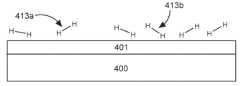
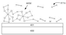
도 4a 내지 도 4j는 WCl6로부터 텅스텐의 증착에서 증착 사이클의 예시적인 메커니즘의 개략적인 예시들이다. 도 4a는 H2가 그 위에 증착된 하부 층 (401) 을 갖는 기판 (400) 에 도입되는 예시적인 메커니즘을 도시한다. 하부 층 (401) 은 일부 실시예들에서 배리어 층일 수도 있다. 예를 들어, 일부 실시예들에서, 하부 층 (401) 은 티타늄 나이트라이드 (TiN) 층이다. 일부 실시예들에서, 기판 (400) 은 텅스텐 핵생성 층을 포함하지 않는다는 것을 주의한다. 다른 실시예들에서, 이는 텅스텐 핵생성 층을 포함할 수도 있다. 수소가 가스 상 (411a 및 411b) 으로 도입되고 일부 H2 (413a 및 413b) 는, 금속 표면들 (예를 들어 H2) 상에 화학적으로 활성 흡착되고 비활성 표면들 (예를 들어 TiN) 상에 촉매로 물리흡착된 원자 수소로 촉매로 해리될 수도 있는, 하부 층 (401) 의 표면 상에 있다. 예를 들어, H2는 하부 층 (401) 상에 화학흡착할 필요가 없을 수도 있고, 일부 실시예들에서, 하부 층 (401) 의 표면 상에 물리흡착할 수도 있다.
도 4b는 이전에 가스 상인 H2 (도 4a의 411a 및 411b) 가 챔버로부터 퍼지되고, 이전에 표면 (443a 및 413b) 상의 H2가 하부 층 (401) 의 표면 상에 남아 있는 예시적인 예시를 도시한다.
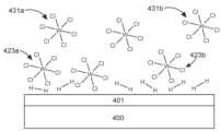
도 4c는 기판이 WCl6에 노출되고, 이들 중 일부는 가스 상 (431a 및 431b) 이고 이들 중 일부는 기판의 표면에 있거나 근방에 (423a 및 423b) 있는 예시적인 예시를 도시한다.
동작 200 동안, 일부 H2는 이전 도즈로부터 표면 상에 남아 있는 WCl6와 반응할 수도 있다. 도 4d에서, WCl6는 중간물 (443b) 을 일시적으로 형성하도록 H2와 반응할 수도 있고, 도 4e에서, 중간물 (443b) 은 하부 층 (401) 상에 기판 (400) 의 표면 상에 텅스텐 (490), 그리고 가스 상의 HCl (451a 및 451b, 예를 들어) 을 남기도록 완전히 반응한다. 이 예에서, 텅스텐 (490) 은 텅스텐을 증착하기 전, 하부 층 (401) 을 처리하지 않고 핵생성 층을 증착하지 않고 하부 층 (401) 직상에 성장한다는 것을 주의한다. 일부 실시예들에서, 하부 층 (401) 을 수소 또는 염소-함유 텅스텐 전구체에 노출하기 전, 하부 층 (401) 은, 예컨대 디보란에 노출함으로써 소킹 처리에 노출될 수도 있다는 것이 이해될 것이다. 일부 예들에서 하부 층 (401) 은 후속하는 WClx-H2 노출들 동안 희생적으로 반응할 수 있는 단단한 Si-B-H 계면 표면 층을 형성하도록 SiH4, B2H6, 및 H2의 혼합물로 이전에 처리되었다. Si-B-H 층들의 화학량론은 저 붕소 농도 (10 %) 로부터 고 붕소 농도 (95 %) 로 크게 가변할 수 있다.
도 2a 내지 도 2c의 동작 200 동안, 일부 H2 는 이전 도즈로부터 표면 상에 남아 있는 WCl6 (또는 다른 W 클로라이드들) 과 완전히 반응하지 않을 수도 있다. 도 4d에 도시된 바와 같이, WCl6는 중간물 (443a) 을 형성하도록 H2와 부분적으로 반응할 수도 있고, 도 4e에서, 나머지 중간물 (443a) 은 하부 층 (401) 상의 기판 (400) 의 표면 상에서 부분적으로 반응한다. 다양한 실시예들에서, 염소-함유 텅스텐 전구체 및 수소를 사용하여 증착된 막은 약 50 Å까지의 증착 두께들에 대해 보란, 실란 또는 게르만을 사용하여 증착된 막보다 낮은 저항률을 갖는다. 예를 들어, 특정한 이론에 제한되지 않고, WCl6의 화학량론은 일 분자의 WCl6와 적어도 3 개의 H2 분자들을 사용할 수도 있다. WCl6는 텅스텐을 형성하는 대신 중간물이 형성되는, H2의 분자들과 부분적으로 반응하는 것이 가능하다. 예를 들어, 이는 화학량론 원리들에 기초하여 (예를 들어, 3 개의 H2 분자들이 일 분자의 WCl6와 반응하도록 사용된) WCl6와 반응하도록 인접하여 충분한 H2가 없으면 발생할 수도 있어, 기판의 표면 상에 중간물 (443a) 을 남긴다. 텅스텐 클로라이드들은 분자 H2 에 화학적으로 불활성일 수도 있고 분자 H2의 촉매 해리에 의해 생성된 흡착된 원자 수소의 존재를 필요로 할 수도 있다. 이 경우 과도한 분자 H2는 텅스텐 클로라이드들을 금속성 텅스텐으로 완전히 환원하기 위해 필요할 수도 있는 단순한 화학량론 비를 넘는다 (100 대 1의 분자 H2 / WClx 비).
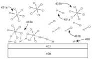
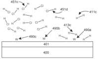
도 4f는 챔버가 퍼지될 때 기판의 예시적인 개략도를 제공한다. 이는 도 2a 내지 도 2c의 동작 202에 대응할 수도 있다. 도 4f의 화합물 (443c) 은 완전히 반응하지 않은 형성된 중간물일 수도 있지만, 일부 텅스텐 (490) 이 기판 상에 형성될 수도 있다는 것을 주의한다. 이에 따라 사이클 각각은 기판 상에 텅스텐의 반-모노레이어를 형성한다.
예로서, 도 4g는 사이클이 반복될 때, 가스 상의 H2(411c) 가 증착된 텅스텐 (490) 및 그 위에 부분적으로 반응된 중간물 (443d) 을 갖는 기판에 도입되는 예시를 도시한다. 이는 텅스텐이 적절한 두께로 증착되지 않았다고 동작 208에서 결정된 후 반복된 사이클에서 도 2a 내지 도 2c의 동작 200에 대응할 수도 있다. 도 4g에 도시된 바와 같이, 도입된 H2는 이제 도 4h에 도시된 바와 같이, 반복된 화합물 (443d) 은 증착된 텅스텐 (490b 및 490c) 을 넘어 떠나고, 그리고 생성물들 HCl (451c 및 451d) 에 의해 가스 상에 형성되도록 기판 상의 중간물 (443d) 과 완전히 반응할 수도 있다는 것을 주의한다. 일부 H2(411c) 가 가스 상으로 남을 수도 있지만, 일부 H2(413c) 는 텅스텐 층 (490a) 상에 남아 있을 수도 있다.
도 4i에서, (도 2a 내지 도 2c의 동작 202에 대응하여) 챔버는 퍼지되어, 텅스텐 (490a, 490b, 및 490c), 및 일부 H2(413c) 를 넘어 떠난다. 도 4j에서, WCl6는 분자들 (431c 및 423c) 이 H2 및 기판에 흡착 및/또는 퍼지할 수도 있도록 도즈로 다시 도입된다. 도 4j는 도 2a 내지 도 2c의 동작 204에 대응할 수도 있다. WCl6 도즈 후, 챔버는 다시 퍼지될 수도 있고 사이클들이 목표된 두께의 텅스텐이 증착될 때까지 다시 반복될 수도 있다.
특정한 개시된 실시예들을 사용하여 증착된 텅스텐 막들은 불소 함량을 갖지 않는다. 몰리브덴 막들이 또한 불소 함량을 갖지 않을 수도 있다. 막들의 전체 인장 응력이 약 0.2 GPa보다 작을 수도 있다. 불소-프리 텅스텐 전구체들은 텅스텐 펜타클로라이드 (WCl5) 및 텅스텐 헥사클로라이드 (WCl6) 와 같은 텅스텐 카르보닐 (W(CO)6) 및 텅스텐 클로라이드들 (WClx) 을 포함할 수도 있다. 불소-프리 몰리브덴 전구체들은 본 명세서에 기술된 몰리브덴 옥시클로라이드 및 몰리브덴 클로라이드 전구체들 뿐만 아니라 몰리브덴 헥사카르보닐 (Mo(CO)6) 을 포함한다.
개시된 실시예들은 텅스텐 및 몰리브덴 증착 프로세스들의 다양한 적용예들을 가질 수도 있다. 본 명세서에 기술된 적용예들의 다양한 조합들은 텅스텐 또는 몰리브덴을 증착하도록 사용될 수도 있고 방법들은 본 명세서에 제공된 예들로 제한되지 않는다는 것이 이해될 것이다.
예를 들어, 일부 실시예들에서, 피처가 환원제 (예를 들어, 수소와 보론, 실란, 또는 게르만) 및 텅스텐 전구체 예컨대 WCl6의 교번하는 펄스들의 ALD 사이클들에 의해 텅스텐 핵생성 층을 증착하고, 이어서 도 2 및 도 3에 대해 상기 기술된 바와 같이 수소 및 염소-함유 텅스텐 전구체의 교번하는 펄스들에 의해 벌크 텅스텐을 증착함으로써 충진될 수도 있다. 유사하게, 일부 실시예들에서, 피처가 환원제 및 몰리브덴 전구체의 교번하는 펄스들의 ALD 사이클들에 의해 몰리브덴 층을 증착함으로써 충진될 수도 있다. 텅스텐 클로라이드 전구체 및 수소 환원제의 교번하는 펄스들을 사용하는 프로세스에 의한 벌크 텅스텐의 증착은 반응물질들의 교번하는 펄스들로 인해 ALD 프로세스들로서 지칭될 수도 있다. 본 명세서에 기술된 방법들은 통상적으로 CVD 메커니즘으로부터 컴포넌트 성장이 없다는 것을 보장하도록 반응물질 사이클들 사이에 퍼지를 수반한다.
그러나, 일부 실시예들에서, 방법들은 미국 특허 공개 번호 제 20170117155 호 및 미국 특허 제 9,613,818 호에 기술된 바와 같이 "순차적 CVD" 프로세스들과 함께 사용될 수도 있고, 양자는 참조로서 본 명세서에 인용된다.
단일 증착 사이클 동안 교번하는 전구체 및 퍼지 가스 펄스들의 복수의 사이클들을 채용함으로써, 전구체는 구조체들의 상단부 및 측방향 에지들에서 에칭을 최소화하여 3D NAND 워드라인들 내로 깊이 전달될 수 있다. 전구체의 모노레이어 또는 반-모노레이어는 구조체 전반에 흡착될 수 있다. 일부 실시예들에서, 교번하는 전구체 및 퍼지 펄스들을 갖는 것은 전구체 도즈 전달 전 가압될 전구체 저장부를 인에이블한다. 이는 구조체로 보다 우수한 이송을 발생시킬 수 있다.
표 1은 H2/Ar/WClx/Ar 시퀀스 및 H2/Ar/n(WClx/Ar) 시퀀스에 노출된 300 Å PVD TiN 블랭킷 막들에 대한 조건들 및 발생하는 TiN 하부 층을 도시하고,n은 10과 같다.
| 프로세스 | 하부 층 | W 도즈 시간 | Ar 퍼지 시간 | 사이클들 | 분압 * 지속기간 (W Torr-S)* 1000 | TiN 에칭 (Å) |
| FFW 10 W/Ar 펄스들 0.5 % W | 300A PVD TiN | x | y | 10z | 250 | 144 |
| FFW 1 W/Ar 펄스들 0.5 % W | 300A PVD TiN | 10x | 10y | z | 250 | 300 |
표 1의 조건들 및 결과들은 동일한 전체 텅스텐 전구체 노출에 대해, 에칭된 TiN의 양은 복수의 펄스들의 텅스텐 전구체를 사용하여 상당히 낮다는 것을 도시한다. 특히, TiN 전체는 단일 텅스텐 전구체 펄스를 갖는 시퀀스 동안 에칭된다.
도 5는 H2/Ar/WClx/Ar 시퀀스 및 H2/Ar/n(WClx/Ar) 시퀀스를 사용하여 3-D NAND 구조체들의 텅스텐 충진을 비교하는 실험 결과들의 개략적 예시를 도시한다. 핵생성 층이 이들 시퀀스들 전에 구조체 각각에 증착된다. 도 5의 예시들은 3-D NAND 구조체들의 중간 섹션들로부터 단면의 표현이다. 3-D NAND 구조체 (503) 는 H2/Ar/WClx/Ar 시퀀스 후 이미지이고, 511에 나타낸 바와 같이, 중심 워드라인들에서 불량한 텅스텐 증착을 도시한다. 균일한 텅스텐 증착은 H2/Ar/n(WClx/Ar) 에 노출되는, 3-D NAND 구조체 (503) 전반에서 관찰되고,n= 10이다. Torr-s의 총 텅스텐 전구체 노출이 501 및 503 모두에 동일하다.
n텅스텐 펄스들 각각은 짧고 일정한 압력으로 전달될 수도 있다. 텅스텐 전구체의 총 양은 텅스텐 전구체가 구조체의 하단부에 도달하고 전체 구조체를 측방향으로 코팅하도록 충분한 재료를 제공하는데 충분하다. 개입되는 불활성 가스 퍼지는 구조체의 상단부 및 에지들에서 텅스텐 전구체를 제거할 수도 있어, 기판 에칭을 감소시키거나 제거한다. 충분한 불활성 가스 퍼지가 없다면, 이 유리한 효과는 관찰되지 않을 수도 있다. 또한, 주변 개구부들에서 핀치 효과가 복수의 텅스텐 펄스들 사이 불충분한 퍼지에 대해 관찰될 수도 있다.
이에 따라, 일부 실시예들에서, 불활성 가스 퍼지의 지속기간은 적어도 텅스텐 또는 몰리브덴 전구체 지속기간만큼 길다. 일부 실시예들에서, 불활성 가스 퍼지는 텅스텐 또는 몰리브덴 전구체 펄스의 지속기간의 적어도 1.5 배 또는 적어도 2 배 또는 적어도 3 배이다. 전구체 노출에 대한 퍼지 가스는 또한 분압 × 지속기간의 면에서 특징화될 수도 있다. 퍼지는 플로우의 1 % 내지 5 %로 희석된 전구체와 함께, 100 % 퍼지 가스로 수행될 수도 있다.
상기 기술은 텅스텐 클로라이드들로부터 텅스텐 및 텅스텐-함유 층들의 증착에 포커싱하지만, 도 2 및 도 3을 참조하여 상기 기술된 프로세스들은 다른 전구체들 및/또는 다른 재료들을 사용한 피처 충진과 함께 수행될 수도 있다. 상기 나타낸 바와 같이, 방법은 구조체를 에칭할 수 있는 화학물질들에 대해 유리하다. 이에 더하여, 복수의 전구체 펄스/퍼지 사이클들을 포함하는 방법은 흡착되지 않은 분자들을 퍼지함으로써 CVD-타입 특성 없이 성장을 달성하는데 유리할 수도 있다.
개시된 실시예들은 임의의 적합한 압력, 약 10 Torr보다 큰 압력들, 또는 약 10 Torr보다 작은 압력들에서 수행될 수도 있다. 멀티-스테이션 챔버에 대해, 페데스탈 각각은 상이한 온도들로 설정될 수도 있다. 일부 실시예들에서, 페데스탈 각각은 동일한 온도로 설정된다. 기판들은 개시된 실시예들에 따른 상기 기술된 동작들 중 임의의 동작 또는 임의의 모든 동작들 동안 스테이션간 (from station to station) 순환될 수도 있다. 챔버 압력은 또한 특정한 개시된 실시예들의 하나 이상의 동작들에서 조절될 수도 있다. 일부 실시예들에서, 핵생성 증착 동안 챔버 압력은 벌크 증착 동안 챔버 압력과 상이하다. 일부 실시예들에서, 핵생성 증착 동안 챔버 압력은 벌크 증착 동안 챔버 압력과 동일하다.
장치
임의의 적합한 챔버가 개시된 실시예들을 구현하도록 사용될 수도 있다. 예시적인 증착 장치들은 다양한 시스템들, 예를 들어, California, Fremont 소재의 Lam Research Corp.로부터 입수가능한 ALTUS® 및 ALTUS® Max 또는 임의의 다양한 다른 상업적으로 입수가능한 프로세싱 시스템들을 포함한다. 일부 실시예들에서, 순차 CVD가 단일 증착 챔버 내에 위치된 2, 5 또는 훨씬 보다 많은 증착 스테이션들 중 하나인 제 1 스테이션에서 수행될 수도 있다. 따라서, 예를 들어, 수소 (H2) 및 텅스텐 헥사클로라이드 (WCl6) 는 기판 표면에서 국부화된 대기를 생성하는 개별 가스 공급 시스템을 사용하여 제 1 스테이션에서 반도체 기판의 표면에 교번하는 펄스들로 도입될 수도 있다. 또 다른 스테이션이 불소-프리 텅스텐 증착, 또는 CVD를 위해 사용될 수도 있다. 2 이상의 스테이션들이 병렬 프로세싱으로 텅스텐을 증착하도록 사용될 수도 있다. 대안적으로, 웨이퍼가 순차적 CVD 동작들이 2 이상의 스테이션들에 걸쳐 순차적으로 수행되게 하도록 인덱싱될 수도 있다.
도 6은 실시예들에 따른 증착 프로세스들을 수행하기 적합한 프로세스 시스템의 개략도이다. 시스템 (600) 은 이송 모듈 (603) 을 포함한다. 이송 모듈 (603) 은 다양한 반응 모듈들 사이에서 이동될 때 프로세싱될 기판들의 오염 위험을 최소화하도록 클린, 가압된 분위기를 제공한다. 다양한 실시예들에 따라 ALD 및 CVD를 수행할 수 있는 멀티-스테이션 반응기 (609) 가 이송 모듈 (603) 상에 장착된다. 멀티-스테이션 반응기 (609) 는 개시된 실시예들에 따른 동작들을 순차적으로 수행할 수도 있는 복수의 스테이션들 (611, 613, 615, 및 617) 을 포함할 수도 있다. 예를 들어, 멀티-스테이션 반응기 (609) 는 스테이션 (611) 이 염소-함유 텅스텐 전구체 또는 불소-함유 전구체를 사용하여 PNL 텅스텐 핵생성 층 증착을 수행하고, 그리고 스테이션 (613) 은 다양한 실시예들에 따른 ALD 텅스텐 증착 동작을 수행하도록 구성될 수도 있다. 일부 실시예들에서, 스테이션 (615) 은 ALD 텅스텐 증착 동작을 수행할 수도 있고, 그리고 스테이션 (617) 은 비순차적 CVD 동작을 수행할 수도 있다. 일부 실시예들에서, 텅스텐 전구체 펄스들의 수 (n) 는 스테이션 (613 내지 615) 으로부터 가변할 수도 있다.
스테이션들은 가열된 페데스탈 또는 기판 지지부, 하나 이상의 가스 유입구들 또는 샤워헤드 또는 확산 플레이트를 포함할 수도 있다. 기판 지지부 (702) 및 샤워헤드 (703) 를 포함하는, 증착 스테이션 (700) 의 일 예가 도 7에 도시된다. 히터가 페데스탈 부분 (701) 에 제공될 수도 있다.
도 6을 다시 참조하면, 플라즈마 또는 화학적 (비플라즈마) 사전-세정, 다른 증착 동작들, 또는 에칭 동작들을 수행할 수 있는 하나 이상의 단일 스테이션 모듈 또는 멀티-스테이션 모듈들 (607) 이 또한 이송 모듈 (503) 상에 장착될 수도 있다. 모듈은 또한 예를 들어, 증착 프로세스를 위해 기판을 준비하도록 다양한 처리들에 사용될 수도 있다. 시스템 (600) 은 또한 웨이퍼들이 프로세싱 전 후에 저장되는, 하나 이상의 웨이퍼 소스 모듈들 (601) 을 포함한다. 대기 이송 챔버 (619) 의 대기 로봇 (미도시) 이 소스 모듈들 (601) 로부터 로드록 (621) 으로 웨이퍼들을 먼저 제거할 수도 있다. 이송 모듈 (603) 의 웨이퍼 이송 디바이스 (일반적으로 로봇 암 유닛) 는 로드록 (621) 으로부터 이송 모듈 (603) 상에 장착된 모듈들 사이에 웨이퍼들을 이동시킨다.
다양한 실시예들에서, 시스템 제어기 (629) 가 증착 동안 프로세스 조건들을 제어하기 위해 채용된다. 제어기 (629) 는 통상적으로 하나 이상의 메모리 디바이스들 및 하나 이상의 프로세서들을 포함할 것이다. 프로세서는 CPU 또는 컴퓨터, 아날로그 입력/출력 연결부 및/또는 디지털 입력/출력 연결부, 스텝퍼 모터 제어 보드들, 등을 포함할 수도 있다.
제어기 (629) 는 증착 장치의 모든 액티비티들을 제어할 수도 있다. 시스템 제어기 (629) 는 타이밍, 가스들의 혼합물, 챔버 압력, 챔버 온도, 웨이퍼 온도, RF (radio frequency) 전력 레벨들, 웨이퍼 척 또는 페데스탈 위치, 및 특정한 프로세스의 다른 파라미터들을 제어하기 위한 인스트럭션들의 세트들을 포함하는, 시스템 제어 소프트웨어를 실행한다. 일부 실시예들에서 제어기 (629) 와 연관된 메모리 디바이스들 상에 저장된 다른 컴퓨터 프로그램들이 채용될 수도 있다.
통상적으로, 제어기 (629) 와 연관된 사용자 인터페이스가 있을 것이다. 사용자 인터페이스는 디스플레이 스크린, 장치 및/또는 프로세스 조건들의 그래픽 소프트웨어 디스플레이들, 포인팅 디바이스들, 키보드들, 터치 스크린들, 마이크로폰들, 등과 같은 사용자 입력 디바이스들을 포함할 수도 있다.
시스템 제어 로직은 임의의 적합한 방식으로 구성될 수도 있다. 일반적으로, 로직은 하드웨어 및/또는 소프트웨어로 구성되거나 설계될 수 있다. 구동 회로를 제어하기 위한 인스트럭션들은 하드코딩될 수도 있고 또는 소프트웨어로서 제공될 수도 있다. 인스트럭션들은 "프로그래밍"에 의해 제공될 수도 있다. 이러한 프로그래밍은 DSPs (digital signal processors), ASICs (application-specific integrated circuits), 및 하드웨어로서 구현된 특정한 알고리즘들을 갖는 다른 디바이스들을 포함하는 임의의 형태의 로직을 포함하는 것으로 이해된다. 프로그래밍은 또한 범용 프로세서 상에서 실행될 수도 있는 소프트웨어 또는 펌웨어 인스트럭션들을 포함하는 것으로 이해된다. 시스템 제어 소프트웨어가 임의의 적합한 컴퓨터 판독가능 프로그램 언어로 코딩될 수도 있다.
프로세스 시퀀스의 게르마늄-함유 환원제 펄스들, 수소 플로우, 및 텅스텐-함유 전구체 펄스들, 및 다른 프로세스들을 제어하기 위한 컴퓨터 프로그램 코드는 임의의 종래의 컴퓨터 판독가능 프로그래밍 언어: 예를 들어, 어셈블리어, C, C++, Pascal, Fortran, 등으로 작성될 수 있다. 컴파일링된 객체 코드 또는 스크립트가 프로그램에서 식별된 태스크들을 수행하도록 프로세서에 의해 실행된다. 또한 나타낸 바와 같이, 프로그램 코드는 하드코딩될 수도 있다.
제어기 파라미터들은, 예를 들어, 프로세스 가스 조성 및 플로우 레이트들, 온도, 압력, 냉각 가스 압력, 기판 온도, 및 챔버 벽 온도와 같은 프로세스 조건들에 관련된다. 이들 파라미터들은 사용자 인터페이스를 활용하여 입력될 수도 있고 레시피의 형태로 사용자들에게 제공된다.
프로세스를 모니터링하기 위한 신호들은 시스템 제어기 (629) 의 아날로그 입력 연결부 및/또는 디지털 입력 연결부에 의해 제공될 수도 있다. 프로세스를 제어하기 위한 신호들은 증착 장치 (600) 의 아날로그 출력 연결부 및 디지털 출력 연결부 상에 출력된다.
시스템 소프트웨어는 많은 다양한 방식들로 설계되거나 구성될 수도 있다. 예를 들어, 다양한 챔버 컴포넌트 서브루틴들 또는 제어 객체들이 개시된 실시예들에 따른 증착 프로세스들을 수행하기 위해 필요한 챔버 컴포넌트들의 동작을 제어하도록 작성될 수도 있다. 이 목적을 위한 프로그램들 또는 프로그램들의 섹션들의 예들은 기판 포지셔닝 코드, 프로세스 가스 제어 코드, 압력 제어 코드, 및 히터 제어 코드를 포함한다.
일부 구현예들에서, 제어기 (629) 는 상기 기술된 예들의 일부일 수도 있는 시스템의 일부이다. 이러한 시스템들은, 프로세싱 툴 또는 툴들, 챔버 또는 챔버들, 프로세싱용 플랫폼 또는 플랫폼들, 및/또는 특정 프로세싱 컴포넌트들 (웨이퍼 페데스탈, 가스 플로우 시스템, 등) 을 포함하는, 반도체 프로세싱 장비를 포함할 수 있다. 이들 시스템들은 반도체 웨이퍼 또는 기판의 프로세싱 이전에, 프로세싱 동안에 그리고 프로세싱 이후에 그들의 동작을 제어하기 위한 전자장치에 통합될 수도 있다. 전자장치는 시스템 또는 시스템들의 다양한 컴포넌트들 또는 하위부분들을 제어할 수도 있는 "제어기"로서 지칭될 수도 있다. 제어기 (629) 는, 시스템의 프로세싱 요건들 및/또는 타입에 따라서, 프로세싱 가스들의 전달, 온도 설정사항들 (예를 들어, 가열 및/또는 냉각), 압력 설정사항들, 진공 설정사항들, 전력 설정사항들, 일부 시스템들에서 무선 주파수 (RF) 생성기 설정사항들, RF 매칭 회로 설정사항들, 주파수 설정사항들, 플로우 레이트 설정사항들, 유체 전달 설정사항들, 위치 및 동작 설정사항들, 툴 및 다른 이송 툴들 및/또는 특정 시스템과 연결되거나 인터페이싱된 로드록들 내외로의 웨이퍼 이송들을 포함하는, 본 명세서에 개시된 프로세스들 중 임의의 프로세스들을 제어하도록 프로그래밍될 수도 있다.
일반적으로 말하면, 제어기는 인스트럭션들을 수신하고, 인스트럭션들을 발행하고, 동작을 제어하고, 세정 동작들을 인에이블하고, 엔드 포인트 측정들을 인에이블하는, 등을 하는 다양한 집적 회로들, 로직, 메모리, 및/또는 소프트웨어를 갖는 전자장치로서 규정될 수도 있다. 집적 회로들은 프로그램 인스트럭션들을 저장하는 펌웨어의 형태의 칩들, 디지털 신호 프로세서들 (DSP), ASICs (Application Specific Integrated Circuits) 로서 규정되는 칩들, 및/또는 프로그램 인스트럭션들 (예를 들어, 소프트웨어) 을 실행하는 하나 이상의 마이크로프로세서들, 또는 마이크로제어기들을 포함할 수도 있다. 프로그램 인스트럭션들은 반도체 웨이퍼 상에서 또는 반도체 웨이퍼에 대한 특정 프로세스를 실행하기 위한 동작 파라미터들을 규정하는, 다양한 개별 설정사항들 (또는 프로그램 파일들) 의 형태로 제어기로 또는 시스템으로 전달되는 인스트럭션들일 수도 있다. 일부 실시예들에서, 동작 파라미터들은 하나 이상의 층들, 재료들, 금속들, 옥사이드들, 실리콘, 실리콘 다이옥사이드, 표면들, 회로들, 및/또는 웨이퍼의 다이들의 제조 동안에 하나 이상의 프로세싱 단계들을 달성하도록 프로세스 엔지니어들에 의해서 규정된 레시피의 일부일 수도 있다.
제어기 (629) 는, 일부 구현예들에서, 시스템에 포함되거나, 시스템에 커플링되거나, 이와 달리 시스템에 네트워킹되거나, 또는 이들의 조합으로 될 수 있는 컴퓨터에 커플링되거나 이의 일부일 수도 있다. 예를 들어, 제어기 (629) 는 웨이퍼 프로세싱의 원격 액세스를 가능하게 할 수 있는 공장 (fab) 호스트 컴퓨터 시스템의 전부 또는 일부이거나 "클라우드" 내에 있을 수도 있다. 컴퓨터는 제조 동작들의 현 진행을 모니터링하고, 과거 제조 동작들의 이력을 조사하고, 복수의 제조 동작들로부터 경향들 또는 성능 계측치들을 조사하고, 현 프로세싱의 파라미터들을 변경하고, 현 프로세싱을 따르는 프로세싱 단계들을 설정하고, 또는 새로운 프로세스를 시작하기 위해서 시스템으로의 원격 액세스를 인에이블할 수도 있다. 일부 예들에서, 원격 컴퓨터 (예를 들어, 서버) 는 로컬 네트워크 또는 인터넷을 포함할 수도 있는 네트워크를 통해서 프로세스 레시피들을 시스템에 제공할 수 있다. 원격 컴퓨터는 차후에 원격 컴퓨터로부터 시스템으로 전달될 파라미터들 및/또는 설정사항들의 입력 또는 프로그래밍을 인에이블하는 사용자 인터페이스를 포함할 수도 있다. 일부 예들에서, 제어기는 하나 이상의 동작들 동안에 수행될 프로세스 단계들 각각에 대한 파라미터들을 특정하는, 데이터의 형태의 인스트럭션들을 수신한다. 파라미터들은 제어기가 제어하거나 인터페이싱하도록 구성되는 툴의 타입 및 수행될 프로세스의 타입에 특정적일 수도 있다는 것이 이해되어야 한다. 따라서 상기 기술된 바와 같이, 제어기는 예컨대 본 명세서에 기술된 프로세스들 및 제어들과 같은, 공동의 목적을 향해 함께 네트워킹되고 작동되는 하나 이상의 개별 제어기들을 포함함으로써 분산될 수도 있다. 이러한 목적들을 위한 분산형 제어기의 예는 챔버 상의 프로세스를 제어하도록 조합되는 (예컨대 플랫폼 레벨에서 또는 원격 컴퓨터의 일부로서) 원격으로 위치한 하나 이상의 집적 회로들과 통신하는 챔버 상의 하나 이상의 집적 회로들일 것이다.
비한정적으로, 예시적인 시스템들은 플라즈마 에칭 챔버 또는 모듈, 증착 챔버 또는 모듈, 스핀-린스 챔버 또는 모듈, 금속 도금 챔버 또는 모듈, 세정 챔버 또는 모듈, 베벨 에지 에칭 챔버 또는 모듈, PVD 챔버 또는 모듈, CVD 챔버 또는 모듈, ALD 챔버 또는 모듈, ALE (Atomic Layer Etch) 챔버 또는 모듈, 이온 주입 챔버 또는 모듈, 트랙 (track) 챔버 또는 모듈, 및 반도체 웨이퍼들의 제조 및/또는 제작 시에 사용되거나 연관될 수도 있는 임의의 다른 반도체 프로세싱 시스템들을 포함할 수도 있다.
상술한 바와 같이, 툴에 의해서 수행될 프로세스 단계 또는 단계들에 따라서, 제어기는, 반도체 제작 공장 내의 툴 위치들 및/또는 로드 포트들로부터/로드 포트들로 웨이퍼들의 컨테이너들을 이동시키는 재료 이송 시에 사용되는, 다른 툴 회로들 또는 모듈들, 다른 툴 컴포넌트들, 클러스터 툴들, 다른 툴 인터페이스들, 인접 툴들, 이웃하는 툴들, 공장 도처에 위치한 툴들, 메인 컴퓨터, 또 다른 제어기, 또는 툴들 중 하나 이상과 통신할 수도 있다.
제어기 (629) 는 다양한 프로그램들을 포함할 수도 있다. 기판 포지셔닝 프로그램은 기판을 페데스탈 또는 척 상으로 로딩하도록 그리고 기판과 가스 유입구 및/또는 타깃과 같은 챔버의 다른 부분들 사이의 간격을 제어하도록 사용되는 챔버 컴포넌트들을 제어하기 위한 프로그램 코드를 포함할 수도 있다. 프로세스 가스 제어 프로그램은 가스 조성, 플로우 레이트들, 펄스 시간들을 제어하기 위한, 그리고 선택가능하게 챔버 내 압력을 안정화하기 위해 증착 전에 챔버 내로 가스를 흘리기 위한 코드를 포함할 수도 있다. 압력 제어 프로그램은 예를 들어, 챔버의 배기 시스템의 쓰로틀 밸브를 조절함으로써 챔버의 압력을 제어하기 위한 코드를 포함할 수도 있다. 히터 제어 프로그램은 기판을 가열하도록 사용되는 가열 유닛으로 전류를 제어하기 위한 코드를 포함할 수도 있다. 대안적으로, 히터 제어 프로그램은 웨이퍼 척으로 (헬륨과 같은) 열 전달 가스의 전달을 제어할 수도 있다.
증착 동안 모니터링될 수도 있는 챔버 센서들의 예들은 질량 유량 제어기들, 마노미터들 (manometers) 과 같은 압력 센서들, 및 페데스탈 또는 척에 위치된 써모커플들 (thermocouples) 을 포함한다. 적절하게 프로그래밍된 피드백 및 제어 알고리즘들이 목표된 프로세스 조건들을 유지하기 위해 이들 센서들로부터 데이터로 사용될 수도 있다.
장치는 도 8에서 개략적으로 도시된 바와 같이 다양한 가스 분배 라인들에 라인 전하들을 제공하는, 가스 매니폴드 시스템을 포함할 수도 있다. 매니폴드 (804) 는 텅스텐-함유 또는 몰리브덴-함유 전구체 가스 (미도시) 의 소스로부터 입력 (802) 을 갖고, 매니폴드 (811) 는 수소 또는 다른 환원 가스 (미도시) 의 소스로부터 입력 (809) 을 갖고 매니폴드 (821) 는 불활성 퍼지 가스 (미도시) 의 소스로부터 입력 (819) 을 갖는다. 매니폴드들 (804, 811 및 821) 은 전구체 가스, 환원 가스 및 퍼지 가스를 각각 밸브 연결된 (valved) 분배 라인들 (805, 813 및 825) 을 통해 증착 챔버로 제공한다. 다양한 밸브들은 라인 전하를 제공하도록, 즉, 분배 라인들을 가압하도록 개방되거나 폐쇄된다. 예를 들어, 분배 라인 (805) 을 가압하기 위해, 밸브 (806) 는 진공에 대해 폐쇄되고, 밸브 (808) 는 폐쇄된다. 적합한 시간 증분 후, 밸브 (808) 가 개방되고 전구체 가스는 챔버로 전달된다. 가스의 전달을 위한 적합한 시간 후, 밸브 (808) 가 폐쇄된다. 이어서 챔버는 진공으로 밸브 (806) 의 개방에 의해 진공으로 퍼지될 수 있다.
유사한 프로세스들이 환원 가스 및 퍼지 가스를 전달하도록 사용된다. 환원 가스를 도입하기 위해, 예를 들어, 분배 라인 (813) 은 진공으로 밸브 (815) 를 폐쇄하고 밸브 (817) 를 폐쇄함으로써 대전된다. 밸브 (815) 의 개방은 챔버로 환원 가스의 전달을 허용한다. 유사하게, 퍼지 가스를 도입하기 위해, 분배 라인 (825) 은 진공으로 밸브 (827) 를 폐쇄하고 밸브 (823) 를 폐쇄함으로써 대전된다. 밸브 (827) 의 개방은 챔버로 아르곤 또는 다른 불활성 퍼지 가스의 전달을 허용한다. 라인 전하들에 대해 허용된 시간 양은 가스의 최초 전달의 양 및 타이밍을 변화시킨다.
도 6은 또한 밸브들 (806, 817 및 823) 각각이 시스템을 퍼지하도록 개방될 수 있는, 진공 펌프들을 도시한다. 다양한 분배 라인들을 통한 가스의 공급은 플로우 레이트들, 플로우의 지속기간, 및 프로세스들의 시퀀스로 프로그래밍되는 마이크로프로세서, 디지털 신호 프로세서, 등에 의해 제어되는 질량 유량 제어기와 같은 제어기에 의해 제어된다.
상기 기술된 프로세스들은 증착 동안 반도체 기판에 시약의 펄스들을 공급하는 밸브들 및 질량 유량 제어기들 (MFCs) 의 정밀한 타이밍을 필요로 할 수도 있다는 것을 주의한다. 이를 가능하게 하는 일 방법에서, 밸브 및 MFC 커맨드들이 PNL 증착 시퀀스의 전부 또는 일부에 대해 모든 시간 임계 커맨드들에 대한 인스트럭션들을 포함하는 정보의 이산 패킷들로 임베딩된 (embedded) 디지털 입력-출력 제어기들 (IOC) 에 전달된다. Lam Research의 ALTUS 시스템은 적어도 하나의 IOC 시퀀스를 제공한다. IOC들은 장치 내의 다양한 지점들; 예를 들어, 프로세스 모듈 내 또는 프로세스 모듈로부터 어느 정도 거리에 서 있는 독립형 전력 랙 상에 물리적으로 위치될 수 있다. 통상적으로 모듈 각각에 복수의 IOC들 (예를 들어, 모듈 당 3) 이 있다. 시퀀스에 포함된 실제 인스트럭션들에 대해, 밸브들을 제어하고 (모든 캐리어 및 반응물질 가스들을 위해) MFCs에 대한 플로우를 설정하기 위한 모든 커맨드들이 단일 IOC 시퀀스에 포함될 수도 있다. 이는 모든 디바이스들의 타이밍이 절대 시각으로부터 그리고 또한 서로 상대적으로 엄격하게 제어된다는 것을 보장한다. 통상적으로 임의의 주어진 시간에 실행하는 복수의 IOC 시퀀스들이 있다. 이는 말하자면, PNL로 하여금 이들 스테이션들에서 PNL-W 핵생성 층을 증착하기 위해 필요한 모든 하드웨어 컴포넌트들에 대해 제어된 모든 타이밍으로 스테이션 1 및 스테이션 2에서 실행되게 한다. 제 2 시퀀스가 동일한 모듈의 다른 증착 스테이션들에서 상기 기술된 타이밍 시퀀스를 사용하여 텅스텐 벌크를 증착하도록 동시에 실행될 수도 있다. 스테이션 3 및 스테이션 4로 시약들의 전달을 제어하는 디바이스들의 상대적인 타이밍은 디바이스들의 그룹에서 중요하지만, 스테이션 1 및 스테이션 2에서 PNL 프로세스의 상대적인 타이밍이 스테이션 3 및 스테이션 4의 상대적인 타이밍으로부터 오프셋될 수 있다. IOC는 패킷화된 시퀀스로 정보를 변환하고 디지털 또는 아날로그 커맨드 신호들을 밸브들을 제어하는 MFC 또는 공압 솔레노이드 뱅크들에 직접 전달한다.
텅스텐-함유 가스의 펄스는 다음과 같이 생성될 수도 있다. 처음에, 시스템은 MFC 또는 다른 플로우-제어 디바이스가 안정화되는 동안 시간의 기간 동안 진공 펌프로 WClx를 방향전환한다. 이는 일 예에서 약 0.5 내지 5 초의 기간 동안 이루어질 수도 있다. 다음에, 시스템은 방향전환 유출구 (606) 및 유출구 (608) 모두를 증착 챔버에 대해 폐쇄함으로써 텅스텐 가스 전달 매니폴드를 가압한다. 이는 예를 들어, 증착 챔버로의 유출구가 개방될 때 시약의 최초 버스트 (burst) 를 생성하기 위해 약 0.1 내지 5 초의 기간 동안 이루어질 수도 있다. 이는 일 예에서 약 0.1 내지 10 초 동안 개구부 유출구 밸브 (808) 에 의해 달성된다. 그 후, 텅스텐-함유 가스는 적합한 퍼지 가스를 사용하여 증착 챔버로부터 퍼지된다. 다른 시약들의 펄싱된 플로우는 유사한 방식으로 이루어질 수도 있다. 몰리브덴-함유 가스의 펄스가 유사한 방식으로 생성될 수도 있다.
전술한 바는 단일 또는 멀티-챔버 반도체 프로세싱 툴의 개시된 실시예들의 구현예를 기술한다. 본 명세서에 기술된 장치 및 프로세스는 예를 들어, 반도체 디바이스들, 디스플레이들, LED들, 광전 패널들 등의 제조 또는 제작을 위해 리소그래픽 패터닝 툴들 또는 프로세스들과 함께 사용될 수도 있다. 통상적으로, 반드시 그러한 것은 아니지만, 이러한 툴들/프로세스들은 공통 제조 설비에서 함께 사용되거나 수행될 것이다. 막의 리소그래픽 패터닝은 통상적으로 단계 각각이 다수의 가능한 툴들과 함께 제공된, 이하의 단계들: (1) 스핀온 (spin-on) 툴 또는 스프레이온 (spray-on) 툴을 사용하여 워크피스, 즉, 기판 상에 포토레지스트를 도포하는 단계; (2) 핫 플레이트 또는 노 또는 UV 경화 툴을 사용하여 포토레지스트를 경화하는 단계; (3) 웨이퍼 스텝퍼와 같은 툴을 사용하여 가시광선 또는 UV 또는 x-선 광에 포토레지스트를 노출시키는 단계; (4) 습식 벤치와 같은 툴을 사용하여 레지스트를 선택적으로 제거하여 레지스트를 패터닝하도록 레지스트를 현상하는 단계; (5) 건식 또는 플라즈마 보조 에칭 툴을 사용함으로써 아래에 놓인 막 또는 워크피스 내로 레지스트 패턴을 전사하는 단계; 및 (6) RF 또는 마이크로파 플라즈마 레지스트 스트립퍼와 같은 툴을 사용하여 레지스트를 제거하는 단계 중 일부 또는 전부를 포함한다.
결론
전술한 실시예들이 이해의 명확성의 목적들을 위해 다소 상세히 기술되었지만, 특정한 변화들 및 수정들이 첨부된 청구항들의 범위 내에서 실시될 수도 있다는 것이 자명할 것이다. 본 실시예들의 프로세스들, 시스템들, 및 장치를 구현하는 많은 대안적인 방식들이 있다는 것에 유의해야 한다. 이에 따라, 본 실시예들은 예시적이고, 제한적이지 않은 것으로 간주될 것이며, 실시예들은 본 명세서에 주어진 세부사항들로 한정되지 않을 것이다.
Claims (38)
- 금속-함유 재료로 충진될 구조체를 제공하는 단계;
상기 구조체를 복수의 증착 사이클들에 노출하는 단계를 포함하고, 증착 사이클 각각은,
복수의 교번하는 수소 (H2) 펄스들 및 불활성 가스 퍼지 펄스들로의 노출로서, 상기 복수의 교번하는 수소 (H2) 펄스들 및 불활성 가스 퍼지 펄스들은 금속 전구체 펄스를 개입시키지 않고 수행되는, 노출; 및
금속 전구체 펄스에 이어 불활성 가스 퍼지 펄스로의 노출을 포함하는, 방법. - 제 1 항에 있어서,
상기 금속은 텅스텐 (W) 또는 몰리브덴 (Mo) 인, 방법. - 제 1 항에 있어서,
상기 금속 전구체는 염소-함유 금속 전구체인, 방법. - 제 3 항에 있어서,
상기 염소-함유 금속 전구체는 텅스텐 클로라이드 또는 텅스텐 옥시클로라이드를 포함하는, 방법. - 제 3 항에 있어서,
상기 염소-함유 금속 전구체는 몰리브덴 클로라이드 또는 몰리브덴 옥시클로라이드를 포함하는, 방법. - 제 3 항에 있어서,
염소-함유 금속 전구체는 WCl5, WCl6, MoCl5, MoO2Cl2, 및 MoOCl4 중 적어도 하나를 포함하는, 방법. - 제 3 항에 있어서,
상기 염소-함유 금속 전구체의 펄스는 체적으로 0.1 % 내지 1.5 %의 염소-함유 텅스텐 금속 전구체를 포함하는, 방법. - 제 1 항에 있어서,
상기 복수의 교번하는 H2 펄스들 및 불활성 가스 퍼지 펄스들로의 노출은 상기 H2 펄스들 동안 상기 불활성 가스 퍼지 플로우를 턴오프하는 것을 포함하는, 방법. - 제 1 항에 있어서,
상기 불활성 가스 퍼지 펄스의 지속기간은 상기 H2 펄스들의 지속기간의 적어도 1.5 배인, 방법. - 제 1 항에 있어서,
증착 사이클 각각은 금속 전구체 펄스를 개입시키지 않고 적어도 5 개의 교번하는 H2 펄스들 및 불활성 가스 퍼지 펄스들을 포함하는, 방법. - 제 1 항에 있어서,
증착 사이클 각각은 금속 전구체 펄스를 개입시키지 않고 적어도 10 개의 교번하는 금속 전구체 펄스들 및 불활성 가스 퍼지 펄스들을 포함하는, 방법. - 제 1 항에 있어서,
증착 사이클 각각은 단일 금속 전구체 펄스만을 포함하는, 방법. - 제 1 항에 있어서,
증착 사이클 각각은 수소 (H2) 펄스를 개입시키지 않고 복수의 교번하는 금속 전구체 펄스들 및 불활성 가스 퍼지 펄스들을 포함하는, 방법. - 제 1 항에 있어서,
상기 구조체는 측벽들 및 개구부들을 통해 유체적으로 액세스가능한 복수의 내부 영역들을 갖는 복수의 피처들로 이어지는 상기 측벽들의 상기 복수의 개구부들을 포함하는 부분적으로 제조된 3차원 (3-D) NAND 구조체인, 방법. - 각각 기판을 홀딩하도록 구성된 하나 이상의 프로세스 챔버들;
수소 (H2) 가스 소스, 금속 전구체 가스 소스, 및 불활성 퍼지 가스 소스에 커플링하기 위한 하나 이상의 프로세스 가스 유입구들; 및
복수의 증착 사이클들을 수행하기 위한 머신-판독가능 인스트럭션들을 포함하는, 장치의 동작들을 제어하기 위한 제어기를 포함하고, 증착 사이클 각각은,
상기 하나 이상의 프로세스 가스 유입구들을 통해 상기 하나 이상의 프로세스 챔버들로 복수의 교번하는 수소 (H2) 펄스들 및 불활성 가스 퍼지 펄스들을 주입하는 단계로서, 상기 복수의 교번하는 수소 (H2) 펄스들 및 불활성 가스 퍼지 펄스들은 금속 전구체 펄스를 개입시키지 않고 수행되는, 상기 복수의 교번하는 수소 (H2) 펄스들 및 불활성 가스 퍼지 펄스들을 주입하는 단계;
상기 하나 이상의 프로세스 가스 유입구들을 통해 상기 하나 이상의 프로세스 챔버들로 금속 전구체 펄스를 주입하는 단계; 및
상기 하나 이상의 프로세스 가스 유입구들을 통해 상기 하나 이상의 프로세스 챔버들로 퍼지 가스 펄스를 주입하는 단계를 포함하는, 장치. - 제 15 항에 있어서,
상기 금속 전구체는 염소-함유 전구체인, 장치. - 제 16 항에 있어서,
상기 금속 전구체는 텅스텐 클로라이드, 텅스텐 옥시클로라이드, 몰리브덴 클로라이드, 및 몰리브덴 옥시클로라이드 중 적어도 하나를 포함하는, 장치. - 금속-함유 재료로 충진될 구조체를 제공하는 단계;
상기 구조체를 복수의 증착 사이클들에 노출하는 단계를 포함하고, 증착 사이클 각각은,
수소 (H2) 펄스로의 노출에 이어 불활성 가스 퍼지 펄스로의 노출; 및
복수의 교번하는 금속 전구체 펄스들 및 불활성 가스 퍼지 펄스들로의 노출을 포함하고,
상기 복수의 교번하는 금속 전구체 펄스들 및 불활성 가스 퍼지 펄스들은 수소 (H2) 펄스를 개입시키지 않고 수행되는, 방법. - 제 18 항에 있어서,
상기 금속은 텅스텐 (W) 또는 몰리브덴 (Mo) 인, 방법. - 제 18 항에 있어서,
상기 금속 전구체는 염소-함유 금속 전구체인, 방법. - 제 20 항에 있어서,
상기 염소-함유 금속 전구체는 텅스텐 클로라이드 또는 텅스텐 옥시클로라이드를 포함하는, 방법. - 제 21 항에 있어서,
상기 염소-함유 금속 전구체는 WCl5 및 WCl6 중 적어도 하나를 포함하는, 방법. - 제 20 항에 있어서,
상기 염소-함유 금속 전구체는 몰리브덴 클로라이드 또는 몰리브덴 옥시클로라이드를 포함하는, 방법. - 제 23 항에 있어서,
염소-함유 금속 전구체는 MoCl5, MoO2Cl2, 및 MoOCl4 중 적어도 하나를 포함하는, 방법. - 제 20 항에 있어서,
상기 염소-함유 금속 전구체의 펄스는 체적으로 0.1 % 내지 1.5 %의 염소-함유 텅스텐 전구체를 포함하는, 방법. - 제 18 항에 있어서,
상기 복수의 교번하는 금속 전구체 펄스들 및 불활성 가스 퍼지 펄스들로의 노출은 상기 금속 전구체 펄스들 동안 상기 불활성 가스 퍼지 플로우를 턴오프하는 것을 포함하는, 방법. - 제 18 항에 있어서,
상기 불활성 가스 퍼지 펄스의 지속기간은 상기 금속 전구체 펄스들의 지속기간의 적어도 1.5 배인, 방법. - 제 18 항에 있어서,
증착 사이클 각각은 수소 (H2) 펄스를 개입시키지 않고 적어도 5 개의 교번하는 금속 전구체 펄스들 및 불활성 가스 퍼지 펄스들을 포함하는, 방법. - 제 18 항에 있어서,
증착 사이클 각각은 수소 (H2) 펄스를 개입시키지 않고 적어도 10 개의 교번하는 금속 전구체 펄스들 및 불활성 가스 퍼지 펄스들을 포함하는, 방법. - 제 18 항에 있어서,
증착 사이클 각각은 단일 H2 펄스만을 포함하는, 방법. - 제 18 항에 있어서,
증착 사이클 각각은 금속 전구체 펄스를 개입시키지 않고 복수의 교번하는 H2 펄스들 및 불활성 가스 퍼지 펄스들을 포함하는, 방법. - 제 18 항에 있어서,
상기 구조체는 측벽들 및 개구부들을 통해 유체적으로 액세스가능한 복수의 내부 영역들을 갖는 복수의 피처들로 이어지는 상기 측벽들의 상기 복수의 개구부들을 포함하는 부분적으로 제조된 3차원 (3-D) NAND 구조체인, 방법. - 각각 기판을 홀딩하도록 구성된 하나 이상의 프로세스 챔버들;
수소 (H2) 가스 소스, 금속 전구체 가스 소스, 및 불활성 퍼지 가스 소스에 커플링하기 위한 하나 이상의 프로세스 가스 유입구들; 및
복수의 증착 사이클들을 수행하기 위한 머신-판독가능 인스트럭션들을 포함하는, 장치의 동작들을 제어하기 위한 제어기를 포함하고, 증착 사이클 각각은,
상기 하나 이상의 프로세스 가스 유입구들을 통해 상기 하나 이상의 프로세스 챔버들로 수소 (H2) 펄스를 주입하는 단계;
상기 H2 펄스를 주입한 후, 상기 하나 이상의 프로세스 가스 유입구들을 통해 상기 하나 이상의 프로세스 챔버로 불활성 퍼지 가스 펄스를 주입하는 단계;
상기 불활성 퍼지 가스 펄스를 주입한 후, 상기 하나 이상의 프로세스 가스 유입구들을 통해 상기 하나 이상의 프로세스 챔버들로 복수의 교번하는 금속 전구체 펄스들 및 불활성 가스 퍼지 펄스들을 주입하는 단계를 포함하고,
상기 복수의 교번하는 금속 전구체 펄스들 및 불활성 가스 퍼지 펄스들은 수소 (H2) 펄스를 개입시키지 않고 수행되는, 장치. - 제 33 항에 있어서,
상기 금속 전구체는 염소-함유 전구체인, 장치. - 제 34 항에 있어서,
상기 금속 전구체는 텅스텐 클로라이드, 텅스텐 옥시클로라이드, 몰리브덴 클로라이드, 및 몰리브덴 옥시클로라이드 중 적어도 하나를 포함하는, 장치. - 제 33 항에 있어서,
상기 인스트럭션들은 상기 금속 전구체 펄스들 동안 상기 불활성 가스 퍼지 플로우를 턴 오프하기 위한 인스트럭션들을 포함하는, 장치. - 제 33 항에 있어서,
상기 불활성 가스 퍼지 펄스들의 지속기간은 상기 금속 전구체 펄스들의 지속기간의 적어도 1.5 배인, 장치. - 제 33 항에 있어서,
증착 사이클 각각은 수소 (H2) 펄스를 개입시키지 않고 적어도 5 개의 교번하는 금속 전구체 펄스들 및 불활성 가스 퍼지 펄스들을 포함하는, 장치.
Applications Claiming Priority (3)
| Application Number | Priority Date | Filing Date | Title |
|---|---|---|---|
| US201862666588P | 2018-05-03 | 2018-05-03 | |
| US62/666,588 | 2018-05-03 | ||
| PCT/US2019/030712WO2019213604A1 (en) | 2018-05-03 | 2019-05-03 | Method of depositing tungsten and other metals in 3d nand structures |
Publications (2)
| Publication Number | Publication Date |
|---|---|
| KR20200140391A KR20200140391A (ko) | 2020-12-15 |
| KR102806630B1true KR102806630B1 (ko) | 2025-05-12 |
Family
ID=68386126
Family Applications (1)
| Application Number | Title | Priority Date | Filing Date |
|---|---|---|---|
| KR1020207034800AActiveKR102806630B1 (ko) | 2018-05-03 | 2019-05-03 | 3d nand 구조체들에 텅스텐 및 다른 금속들을 증착하는 방법 |
Country Status (5)
| Country | Link |
|---|---|
| US (1) | US11549175B2 (ko) |
| JP (2) | JP2021523292A (ko) |
| KR (1) | KR102806630B1 (ko) |
| CN (1) | CN112262457A (ko) |
| WO (1) | WO2019213604A1 (ko) |
Families Citing this family (250)
| Publication number | Priority date | Publication date | Assignee | Title |
|---|---|---|---|---|
| US20130023129A1 (en) | 2011-07-20 | 2013-01-24 | Asm America, Inc. | Pressure transmitter for a semiconductor processing environment |
| US20160376700A1 (en) | 2013-02-01 | 2016-12-29 | Asm Ip Holding B.V. | System for treatment of deposition reactor |
| US10941490B2 (en) | 2014-10-07 | 2021-03-09 | Asm Ip Holding B.V. | Multiple temperature range susceptor, assembly, reactor and system including the susceptor, and methods of using the same |
| US10276355B2 (en) | 2015-03-12 | 2019-04-30 | Asm Ip Holding B.V. | Multi-zone reactor, system including the reactor, and method of using the same |
| US11139308B2 (en) | 2015-12-29 | 2021-10-05 | Asm Ip Holding B.V. | Atomic layer deposition of III-V compounds to form V-NAND devices |
| US10529554B2 (en) | 2016-02-19 | 2020-01-07 | Asm Ip Holding B.V. | Method for forming silicon nitride film selectively on sidewalls or flat surfaces of trenches |
| US10343920B2 (en) | 2016-03-18 | 2019-07-09 | Asm Ip Holding B.V. | Aligned carbon nanotubes |
| US11453943B2 (en) | 2016-05-25 | 2022-09-27 | Asm Ip Holding B.V. | Method for forming carbon-containing silicon/metal oxide or nitride film by ALD using silicon precursor and hydrocarbon precursor |
| US10612137B2 (en) | 2016-07-08 | 2020-04-07 | Asm Ip Holdings B.V. | Organic reactants for atomic layer deposition |
| US9859151B1 (en) | 2016-07-08 | 2018-01-02 | Asm Ip Holding B.V. | Selective film deposition method to form air gaps |
| US9887082B1 (en) | 2016-07-28 | 2018-02-06 | Asm Ip Holding B.V. | Method and apparatus for filling a gap |
| US9812320B1 (en) | 2016-07-28 | 2017-11-07 | Asm Ip Holding B.V. | Method and apparatus for filling a gap |
| US10573522B2 (en) | 2016-08-16 | 2020-02-25 | Lam Research Corporation | Method for preventing line bending during metal fill process |
| US11532757B2 (en) | 2016-10-27 | 2022-12-20 | Asm Ip Holding B.V. | Deposition of charge trapping layers |
| US10714350B2 (en) | 2016-11-01 | 2020-07-14 | ASM IP Holdings, B.V. | Methods for forming a transition metal niobium nitride film on a substrate by atomic layer deposition and related semiconductor device structures |
| KR102546317B1 (ko) | 2016-11-15 | 2023-06-21 | 에이에스엠 아이피 홀딩 비.브이. | 기체 공급 유닛 및 이를 포함하는 기판 처리 장치 |
| US11581186B2 (en) | 2016-12-15 | 2023-02-14 | Asm Ip Holding B.V. | Sequential infiltration synthesis apparatus |
| US11447861B2 (en) | 2016-12-15 | 2022-09-20 | Asm Ip Holding B.V. | Sequential infiltration synthesis apparatus and a method of forming a patterned structure |
| US11390950B2 (en) | 2017-01-10 | 2022-07-19 | Asm Ip Holding B.V. | Reactor system and method to reduce residue buildup during a film deposition process |
| US10468261B2 (en) | 2017-02-15 | 2019-11-05 | Asm Ip Holding B.V. | Methods for forming a metallic film on a substrate by cyclical deposition and related semiconductor device structures |
| US10770286B2 (en) | 2017-05-08 | 2020-09-08 | Asm Ip Holdings B.V. | Methods for selectively forming a silicon nitride film on a substrate and related semiconductor device structures |
| US12040200B2 (en) | 2017-06-20 | 2024-07-16 | Asm Ip Holding B.V. | Semiconductor processing apparatus and methods for calibrating a semiconductor processing apparatus |
| US11306395B2 (en) | 2017-06-28 | 2022-04-19 | Asm Ip Holding B.V. | Methods for depositing a transition metal nitride film on a substrate by atomic layer deposition and related deposition apparatus |
| KR20190009245A (ko) | 2017-07-18 | 2019-01-28 | 에이에스엠 아이피 홀딩 비.브이. | 반도체 소자 구조물 형성 방법 및 관련된 반도체 소자 구조물 |
| US11374112B2 (en) | 2017-07-19 | 2022-06-28 | Asm Ip Holding B.V. | Method for depositing a group IV semiconductor and related semiconductor device structures |
| US10590535B2 (en) | 2017-07-26 | 2020-03-17 | Asm Ip Holdings B.V. | Chemical treatment, deposition and/or infiltration apparatus and method for using the same |
| TWI815813B (zh) | 2017-08-04 | 2023-09-21 | 荷蘭商Asm智慧財產控股公司 | 用於分配反應腔內氣體的噴頭總成 |
| US10770336B2 (en) | 2017-08-08 | 2020-09-08 | Asm Ip Holding B.V. | Substrate lift mechanism and reactor including same |
| US10692741B2 (en) | 2017-08-08 | 2020-06-23 | Asm Ip Holdings B.V. | Radiation shield |
| US11769682B2 (en) | 2017-08-09 | 2023-09-26 | Asm Ip Holding B.V. | Storage apparatus for storing cassettes for substrates and processing apparatus equipped therewith |
| WO2019036292A1 (en) | 2017-08-14 | 2019-02-21 | Lam Research Corporation | METHOD FOR METAL CASTING FOR THREE-DIMENSIONAL NAND AND VERTICAL WORDS LINE |
| US11830730B2 (en) | 2017-08-29 | 2023-11-28 | Asm Ip Holding B.V. | Layer forming method and apparatus |
| US11295980B2 (en) | 2017-08-30 | 2022-04-05 | Asm Ip Holding B.V. | Methods for depositing a molybdenum metal film over a dielectric surface of a substrate by a cyclical deposition process and related semiconductor device structures |
| US10658205B2 (en) | 2017-09-28 | 2020-05-19 | Asm Ip Holdings B.V. | Chemical dispensing apparatus and methods for dispensing a chemical to a reaction chamber |
| US10403504B2 (en) | 2017-10-05 | 2019-09-03 | Asm Ip Holding B.V. | Method for selectively depositing a metallic film on a substrate |
| US10923344B2 (en) | 2017-10-30 | 2021-02-16 | Asm Ip Holding B.V. | Methods for forming a semiconductor structure and related semiconductor structures |
| CN111344522B (zh) | 2017-11-27 | 2022-04-12 | 阿斯莫Ip控股公司 | 包括洁净迷你环境的装置 |
| WO2019103613A1 (en) | 2017-11-27 | 2019-05-31 | Asm Ip Holding B.V. | A storage device for storing wafer cassettes for use with a batch furnace |
| US10872771B2 (en) | 2018-01-16 | 2020-12-22 | Asm Ip Holding B. V. | Method for depositing a material film on a substrate within a reaction chamber by a cyclical deposition process and related device structures |
| TWI799494B (zh) | 2018-01-19 | 2023-04-21 | 荷蘭商Asm 智慧財產控股公司 | 沈積方法 |
| KR102695659B1 (ko) | 2018-01-19 | 2024-08-14 | 에이에스엠 아이피 홀딩 비.브이. | 플라즈마 보조 증착에 의해 갭 충진 층을 증착하는 방법 |
| US11081345B2 (en) | 2018-02-06 | 2021-08-03 | Asm Ip Holding B.V. | Method of post-deposition treatment for silicon oxide film |
| WO2019158960A1 (en) | 2018-02-14 | 2019-08-22 | Asm Ip Holding B.V. | A method for depositing a ruthenium-containing film on a substrate by a cyclical deposition process |
| US10896820B2 (en) | 2018-02-14 | 2021-01-19 | Asm Ip Holding B.V. | Method for depositing a ruthenium-containing film on a substrate by a cyclical deposition process |
| US10731249B2 (en) | 2018-02-15 | 2020-08-04 | Asm Ip Holding B.V. | Method of forming a transition metal containing film on a substrate by a cyclical deposition process, a method for supplying a transition metal halide compound to a reaction chamber, and related vapor deposition apparatus |
| KR102636427B1 (ko) | 2018-02-20 | 2024-02-13 | 에이에스엠 아이피 홀딩 비.브이. | 기판 처리 방법 및 장치 |
| US10975470B2 (en) | 2018-02-23 | 2021-04-13 | Asm Ip Holding B.V. | Apparatus for detecting or monitoring for a chemical precursor in a high temperature environment |
| US11473195B2 (en) | 2018-03-01 | 2022-10-18 | Asm Ip Holding B.V. | Semiconductor processing apparatus and a method for processing a substrate |
| KR102646467B1 (ko) | 2018-03-27 | 2024-03-11 | 에이에스엠 아이피 홀딩 비.브이. | 기판 상에 전극을 형성하는 방법 및 전극을 포함하는 반도체 소자 구조 |
| KR102600229B1 (ko) | 2018-04-09 | 2023-11-10 | 에이에스엠 아이피 홀딩 비.브이. | 기판 지지 장치, 이를 포함하는 기판 처리 장치 및 기판 처리 방법 |
| US12025484B2 (en) | 2018-05-08 | 2024-07-02 | Asm Ip Holding B.V. | Thin film forming method |
| US12272527B2 (en) | 2018-05-09 | 2025-04-08 | Asm Ip Holding B.V. | Apparatus for use with hydrogen radicals and method of using same |
| KR102596988B1 (ko) | 2018-05-28 | 2023-10-31 | 에이에스엠 아이피 홀딩 비.브이. | 기판 처리 방법 및 그에 의해 제조된 장치 |
| US11718913B2 (en) | 2018-06-04 | 2023-08-08 | Asm Ip Holding B.V. | Gas distribution system and reactor system including same |
| KR102568797B1 (ko) | 2018-06-21 | 2023-08-21 | 에이에스엠 아이피 홀딩 비.브이. | 기판 처리 시스템 |
| US10797133B2 (en) | 2018-06-21 | 2020-10-06 | Asm Ip Holding B.V. | Method for depositing a phosphorus doped silicon arsenide film and related semiconductor device structures |
| KR102854019B1 (ko) | 2018-06-27 | 2025-09-02 | 에이에스엠 아이피 홀딩 비.브이. | 금속 함유 재료를 형성하기 위한 주기적 증착 방법 및 금속 함유 재료를 포함하는 필름 및 구조체 |
| TWI873894B (zh) | 2018-06-27 | 2025-02-21 | 荷蘭商Asm Ip私人控股有限公司 | 用於形成含金屬材料及包含含金屬材料的膜及結構之循環沉積方法 |
| US10755922B2 (en) | 2018-07-03 | 2020-08-25 | Asm Ip Holding B.V. | Method for depositing silicon-free carbon-containing film as gap-fill layer by pulse plasma-assisted deposition |
| US10388513B1 (en) | 2018-07-03 | 2019-08-20 | Asm Ip Holding B.V. | Method for depositing silicon-free carbon-containing film as gap-fill layer by pulse plasma-assisted deposition |
| US11430674B2 (en) | 2018-08-22 | 2022-08-30 | Asm Ip Holding B.V. | Sensor array, apparatus for dispensing a vapor phase reactant to a reaction chamber and related methods |
| KR102707956B1 (ko) | 2018-09-11 | 2024-09-19 | 에이에스엠 아이피 홀딩 비.브이. | 박막 증착 방법 |
| US11024523B2 (en) | 2018-09-11 | 2021-06-01 | Asm Ip Holding B.V. | Substrate processing apparatus and method |
| CN110970344B (zh) | 2018-10-01 | 2024-10-25 | Asmip控股有限公司 | 衬底保持设备、包含所述设备的系统及其使用方法 |
| KR102592699B1 (ko) | 2018-10-08 | 2023-10-23 | 에이에스엠 아이피 홀딩 비.브이. | 기판 지지 유닛 및 이를 포함하는 박막 증착 장치와 기판 처리 장치 |
| KR102546322B1 (ko) | 2018-10-19 | 2023-06-21 | 에이에스엠 아이피 홀딩 비.브이. | 기판 처리 장치 및 기판 처리 방법 |
| US12378665B2 (en) | 2018-10-26 | 2025-08-05 | Asm Ip Holding B.V. | High temperature coatings for a preclean and etch apparatus and related methods |
| US11087997B2 (en) | 2018-10-31 | 2021-08-10 | Asm Ip Holding B.V. | Substrate processing apparatus for processing substrates |
| KR102748291B1 (ko) | 2018-11-02 | 2024-12-31 | 에이에스엠 아이피 홀딩 비.브이. | 기판 지지 유닛 및 이를 포함하는 기판 처리 장치 |
| US11572620B2 (en) | 2018-11-06 | 2023-02-07 | Asm Ip Holding B.V. | Methods for selectively depositing an amorphous silicon film on a substrate |
| US10818758B2 (en) | 2018-11-16 | 2020-10-27 | Asm Ip Holding B.V. | Methods for forming a metal silicate film on a substrate in a reaction chamber and related semiconductor device structures |
| US12148623B2 (en) | 2018-11-19 | 2024-11-19 | Lam Research Corporation | Deposition of tungsten on molybdenum templates |
| US12040199B2 (en) | 2018-11-28 | 2024-07-16 | Asm Ip Holding B.V. | Substrate processing apparatus for processing substrates |
| KR102636428B1 (ko) | 2018-12-04 | 2024-02-13 | 에이에스엠 아이피 홀딩 비.브이. | 기판 처리 장치를 세정하는 방법 |
| US11158513B2 (en) | 2018-12-13 | 2021-10-26 | Asm Ip Holding B.V. | Methods for forming a rhenium-containing film on a substrate by a cyclical deposition process and related semiconductor device structures |
| TWI874340B (zh) | 2018-12-14 | 2025-03-01 | 荷蘭商Asm Ip私人控股有限公司 | 形成裝置結構之方法、其所形成之結構及施行其之系統 |
| US11972952B2 (en) | 2018-12-14 | 2024-04-30 | Lam Research Corporation | Atomic layer deposition on 3D NAND structures |
| TWI866480B (zh) | 2019-01-17 | 2024-12-11 | 荷蘭商Asm Ip 私人控股有限公司 | 藉由循環沈積製程於基板上形成含過渡金屬膜之方法 |
| CN113366144B (zh) | 2019-01-28 | 2023-07-07 | 朗姆研究公司 | 金属膜的沉积 |
| TWI845607B (zh) | 2019-02-20 | 2024-06-21 | 荷蘭商Asm Ip私人控股有限公司 | 用來填充形成於基材表面內之凹部的循環沉積方法及設備 |
| TWI838458B (zh) | 2019-02-20 | 2024-04-11 | 荷蘭商Asm Ip私人控股有限公司 | 用於3d nand應用中之插塞填充沉積之設備及方法 |
| TWI873122B (zh) | 2019-02-20 | 2025-02-21 | 荷蘭商Asm Ip私人控股有限公司 | 填充一基板之一表面內所形成的一凹槽的方法、根據其所形成之半導體結構、及半導體處理設備 |
| TWI842826B (zh) | 2019-02-22 | 2024-05-21 | 荷蘭商Asm Ip私人控股有限公司 | 基材處理設備及處理基材之方法 |
| US11742198B2 (en) | 2019-03-08 | 2023-08-29 | Asm Ip Holding B.V. | Structure including SiOCN layer and method of forming same |
| KR102858005B1 (ko) | 2019-03-08 | 2025-09-09 | 에이에스엠 아이피 홀딩 비.브이. | 실리콘 질화물 층을 선택적으로 증착하는 방법, 및 선택적으로 증착된 실리콘 질화물 층을 포함하는 구조체 |
| SG11202109796QA (en) | 2019-03-11 | 2021-10-28 | Lam Res Corp | Precursors for deposition of molybdenum-containing films |
| JP2020167398A (ja) | 2019-03-28 | 2020-10-08 | エーエスエム・アイピー・ホールディング・ベー・フェー | ドアオープナーおよびドアオープナーが提供される基材処理装置 |
| KR102809999B1 (ko) | 2019-04-01 | 2025-05-19 | 에이에스엠 아이피 홀딩 비.브이. | 반도체 소자를 제조하는 방법 |
| WO2020210260A1 (en) | 2019-04-11 | 2020-10-15 | Lam Research Corporation | High step coverage tungsten deposition |
| SG11202111547QA (en)* | 2019-04-19 | 2021-11-29 | Lam Res Corp | Rapid flush purging during atomic layer deposition |
| KR20200123380A (ko)* | 2019-04-19 | 2020-10-29 | 에이에스엠 아이피 홀딩 비.브이. | 층 형성 방법 및 장치 |
| KR20200125453A (ko) | 2019-04-24 | 2020-11-04 | 에이에스엠 아이피 홀딩 비.브이. | 기상 반응기 시스템 및 이를 사용하는 방법 |
| KR20200130121A (ko) | 2019-05-07 | 2020-11-18 | 에이에스엠 아이피 홀딩 비.브이. | 딥 튜브가 있는 화학물질 공급원 용기 |
| KR20200130652A (ko) | 2019-05-10 | 2020-11-19 | 에이에스엠 아이피 홀딩 비.브이. | 표면 상에 재료를 증착하는 방법 및 본 방법에 따라 형성된 구조 |
| JP7612342B2 (ja) | 2019-05-16 | 2025-01-14 | エーエスエム・アイピー・ホールディング・ベー・フェー | ウェハボートハンドリング装置、縦型バッチ炉および方法 |
| JP7598201B2 (ja) | 2019-05-16 | 2024-12-11 | エーエスエム・アイピー・ホールディング・ベー・フェー | ウェハボートハンドリング装置、縦型バッチ炉および方法 |
| USD947913S1 (en) | 2019-05-17 | 2022-04-05 | Asm Ip Holding B.V. | Susceptor shaft |
| USD975665S1 (en) | 2019-05-17 | 2023-01-17 | Asm Ip Holding B.V. | Susceptor shaft |
| US12237221B2 (en) | 2019-05-22 | 2025-02-25 | Lam Research Corporation | Nucleation-free tungsten deposition |
| KR20200141002A (ko) | 2019-06-06 | 2020-12-17 | 에이에스엠 아이피 홀딩 비.브이. | 배기 가스 분석을 포함한 기상 반응기 시스템을 사용하는 방법 |
| KR20200141931A (ko) | 2019-06-10 | 2020-12-21 | 에이에스엠 아이피 홀딩 비.브이. | 석영 에피택셜 챔버를 세정하는 방법 |
| KR20200143254A (ko) | 2019-06-11 | 2020-12-23 | 에이에스엠 아이피 홀딩 비.브이. | 개질 가스를 사용하여 전자 구조를 형성하는 방법, 상기 방법을 수행하기 위한 시스템, 및 상기 방법을 사용하여 형성되는 구조 |
| KR20210005515A (ko) | 2019-07-03 | 2021-01-14 | 에이에스엠 아이피 홀딩 비.브이. | 기판 처리 장치용 온도 제어 조립체 및 이를 사용하는 방법 |
| JP7499079B2 (ja) | 2019-07-09 | 2024-06-13 | エーエスエム・アイピー・ホールディング・ベー・フェー | 同軸導波管を用いたプラズマ装置、基板処理方法 |
| CN112216646A (zh) | 2019-07-10 | 2021-01-12 | Asm Ip私人控股有限公司 | 基板支撑组件及包括其的基板处理装置 |
| KR20210010307A (ko) | 2019-07-16 | 2021-01-27 | 에이에스엠 아이피 홀딩 비.브이. | 기판 처리 장치 |
| KR20210010816A (ko) | 2019-07-17 | 2021-01-28 | 에이에스엠 아이피 홀딩 비.브이. | 라디칼 보조 점화 플라즈마 시스템 및 방법 |
| KR102860110B1 (ko) | 2019-07-17 | 2025-09-16 | 에이에스엠 아이피 홀딩 비.브이. | 실리콘 게르마늄 구조를 형성하는 방법 |
| US11643724B2 (en) | 2019-07-18 | 2023-05-09 | Asm Ip Holding B.V. | Method of forming structures using a neutral beam |
| KR20210010817A (ko) | 2019-07-19 | 2021-01-28 | 에이에스엠 아이피 홀딩 비.브이. | 토폴로지-제어된 비정질 탄소 중합체 막을 형성하는 방법 |
| TWI851767B (zh) | 2019-07-29 | 2024-08-11 | 荷蘭商Asm Ip私人控股有限公司 | 用於利用n型摻雜物及/或替代摻雜物選擇性沉積以達成高摻雜物併入之方法 |
| CN112309899A (zh) | 2019-07-30 | 2021-02-02 | Asm Ip私人控股有限公司 | 基板处理设备 |
| US12169361B2 (en) | 2019-07-30 | 2024-12-17 | Asm Ip Holding B.V. | Substrate processing apparatus and method |
| CN112309900A (zh) | 2019-07-30 | 2021-02-02 | Asm Ip私人控股有限公司 | 基板处理设备 |
| US11587814B2 (en) | 2019-07-31 | 2023-02-21 | Asm Ip Holding B.V. | Vertical batch furnace assembly |
| US11587815B2 (en) | 2019-07-31 | 2023-02-21 | Asm Ip Holding B.V. | Vertical batch furnace assembly |
| US11227782B2 (en) | 2019-07-31 | 2022-01-18 | Asm Ip Holding B.V. | Vertical batch furnace assembly |
| CN112323048B (zh) | 2019-08-05 | 2024-02-09 | Asm Ip私人控股有限公司 | 用于化学源容器的液位传感器 |
| CN112342526A (zh) | 2019-08-09 | 2021-02-09 | Asm Ip私人控股有限公司 | 包括冷却装置的加热器组件及其使用方法 |
| KR20220047333A (ko) | 2019-08-12 | 2022-04-15 | 램 리써치 코포레이션 | 텅스텐 증착 |
| USD965044S1 (en) | 2019-08-19 | 2022-09-27 | Asm Ip Holding B.V. | Susceptor shaft |
| USD965524S1 (en) | 2019-08-19 | 2022-10-04 | Asm Ip Holding B.V. | Susceptor support |
| JP2021031769A (ja) | 2019-08-21 | 2021-03-01 | エーエスエム アイピー ホールディング ビー.ブイ. | 成膜原料混合ガス生成装置及び成膜装置 |
| USD979506S1 (en) | 2019-08-22 | 2023-02-28 | Asm Ip Holding B.V. | Insulator |
| KR20210024423A (ko) | 2019-08-22 | 2021-03-05 | 에이에스엠 아이피 홀딩 비.브이. | 홀을 구비한 구조체를 형성하기 위한 방법 |
| US11286558B2 (en) | 2019-08-23 | 2022-03-29 | Asm Ip Holding B.V. | Methods for depositing a molybdenum nitride film on a surface of a substrate by a cyclical deposition process and related semiconductor device structures including a molybdenum nitride film |
| KR20210024420A (ko) | 2019-08-23 | 2021-03-05 | 에이에스엠 아이피 홀딩 비.브이. | 비스(디에틸아미노)실란을 사용하여 peald에 의해 개선된 품질을 갖는 실리콘 산화물 막을 증착하기 위한 방법 |
| CN119980191A (zh) | 2019-08-28 | 2025-05-13 | 朗姆研究公司 | 金属沉积 |
| WO2021046058A1 (en) | 2019-09-03 | 2021-03-11 | Lam Research Corporation | Molybdenum deposition |
| KR102806450B1 (ko) | 2019-09-04 | 2025-05-12 | 에이에스엠 아이피 홀딩 비.브이. | 희생 캡핑 층을 이용한 선택적 증착 방법 |
| KR102733104B1 (ko) | 2019-09-05 | 2024-11-22 | 에이에스엠 아이피 홀딩 비.브이. | 기판 처리 장치 |
| US11562901B2 (en) | 2019-09-25 | 2023-01-24 | Asm Ip Holding B.V. | Substrate processing method |
| CN112593212B (zh) | 2019-10-02 | 2023-12-22 | Asm Ip私人控股有限公司 | 通过循环等离子体增强沉积工艺形成拓扑选择性氧化硅膜的方法 |
| TWI846953B (zh) | 2019-10-08 | 2024-07-01 | 荷蘭商Asm Ip私人控股有限公司 | 基板處理裝置 |
| TW202128273A (zh) | 2019-10-08 | 2021-08-01 | 荷蘭商Asm Ip私人控股有限公司 | 氣體注入系統、及將材料沉積於反應室內之基板表面上的方法 |
| KR20210042810A (ko) | 2019-10-08 | 2021-04-20 | 에이에스엠 아이피 홀딩 비.브이. | 활성 종을 이용하기 위한 가스 분배 어셈블리를 포함한 반응기 시스템 및 이를 사용하는 방법 |
| TWI846966B (zh) | 2019-10-10 | 2024-07-01 | 荷蘭商Asm Ip私人控股有限公司 | 形成光阻底層之方法及包括光阻底層之結構 |
| US12009241B2 (en) | 2019-10-14 | 2024-06-11 | Asm Ip Holding B.V. | Vertical batch furnace assembly with detector to detect cassette |
| US12327762B2 (en) | 2019-10-15 | 2025-06-10 | Lam Research Corporation | Molybdenum fill |
| TWI834919B (zh) | 2019-10-16 | 2024-03-11 | 荷蘭商Asm Ip私人控股有限公司 | 氧化矽之拓撲選擇性膜形成之方法 |
| US11637014B2 (en) | 2019-10-17 | 2023-04-25 | Asm Ip Holding B.V. | Methods for selective deposition of doped semiconductor material |
| KR102845724B1 (ko) | 2019-10-21 | 2025-08-13 | 에이에스엠 아이피 홀딩 비.브이. | 막을 선택적으로 에칭하기 위한 장치 및 방법 |
| KR20210050453A (ko) | 2019-10-25 | 2021-05-07 | 에이에스엠 아이피 홀딩 비.브이. | 기판 표면 상의 갭 피처를 충진하는 방법 및 이와 관련된 반도체 소자 구조 |
| US11646205B2 (en) | 2019-10-29 | 2023-05-09 | Asm Ip Holding B.V. | Methods of selectively forming n-type doped material on a surface, systems for selectively forming n-type doped material, and structures formed using same |
| KR20210054983A (ko) | 2019-11-05 | 2021-05-14 | 에이에스엠 아이피 홀딩 비.브이. | 도핑된 반도체 층을 갖는 구조체 및 이를 형성하기 위한 방법 및 시스템 |
| US11501968B2 (en) | 2019-11-15 | 2022-11-15 | Asm Ip Holding B.V. | Method for providing a semiconductor device with silicon filled gaps |
| KR102861314B1 (ko) | 2019-11-20 | 2025-09-17 | 에이에스엠 아이피 홀딩 비.브이. | 기판의 표면 상에 탄소 함유 물질을 증착하는 방법, 상기 방법을 사용하여 형성된 구조물, 및 상기 구조물을 형성하기 위한 시스템 |
| CN112951697B (zh) | 2019-11-26 | 2025-07-29 | Asmip私人控股有限公司 | 基板处理设备 |
| US11450529B2 (en) | 2019-11-26 | 2022-09-20 | Asm Ip Holding B.V. | Methods for selectively forming a target film on a substrate comprising a first dielectric surface and a second metallic surface |
| CN112885692B (zh) | 2019-11-29 | 2025-08-15 | Asmip私人控股有限公司 | 基板处理设备 |
| CN120432376A (zh) | 2019-11-29 | 2025-08-05 | Asm Ip私人控股有限公司 | 基板处理设备 |
| JP7527928B2 (ja) | 2019-12-02 | 2024-08-05 | エーエスエム・アイピー・ホールディング・ベー・フェー | 基板処理装置、基板処理方法 |
| KR20210070898A (ko) | 2019-12-04 | 2021-06-15 | 에이에스엠 아이피 홀딩 비.브이. | 기판 처리 장치 |
| KR20210078405A (ko) | 2019-12-17 | 2021-06-28 | 에이에스엠 아이피 홀딩 비.브이. | 바나듐 나이트라이드 층을 형성하는 방법 및 바나듐 나이트라이드 층을 포함하는 구조 |
| KR20210080214A (ko) | 2019-12-19 | 2021-06-30 | 에이에스엠 아이피 홀딩 비.브이. | 기판 상의 갭 피처를 충진하는 방법 및 이와 관련된 반도체 소자 구조 |
| JP7730637B2 (ja) | 2020-01-06 | 2025-08-28 | エーエスエム・アイピー・ホールディング・ベー・フェー | ガス供給アセンブリ、その構成要素、およびこれを含む反応器システム |
| JP7636892B2 (ja) | 2020-01-06 | 2025-02-27 | エーエスエム・アイピー・ホールディング・ベー・フェー | チャネル付きリフトピン |
| US11993847B2 (en) | 2020-01-08 | 2024-05-28 | Asm Ip Holding B.V. | Injector |
| EP4091192A4 (en)* | 2020-01-16 | 2024-07-03 | Entegris, Inc. | Method for etching or deposition |
| KR20210093163A (ko) | 2020-01-16 | 2021-07-27 | 에이에스엠 아이피 홀딩 비.브이. | 고 종횡비 피처를 형성하는 방법 |
| KR102675856B1 (ko) | 2020-01-20 | 2024-06-17 | 에이에스엠 아이피 홀딩 비.브이. | 박막 형성 방법 및 박막 표면 개질 방법 |
| TWI889744B (zh) | 2020-01-29 | 2025-07-11 | 荷蘭商Asm Ip私人控股有限公司 | 污染物捕集系統、及擋板堆疊 |
| TW202513845A (zh) | 2020-02-03 | 2025-04-01 | 荷蘭商Asm Ip私人控股有限公司 | 半導體裝置結構及其形成方法 |
| KR20210100010A (ko) | 2020-02-04 | 2021-08-13 | 에이에스엠 아이피 홀딩 비.브이. | 대형 물품의 투과율 측정을 위한 방법 및 장치 |
| US11776846B2 (en) | 2020-02-07 | 2023-10-03 | Asm Ip Holding B.V. | Methods for depositing gap filling fluids and related systems and devices |
| KR20210103956A (ko) | 2020-02-13 | 2021-08-24 | 에이에스엠 아이피 홀딩 비.브이. | 수광 장치를 포함하는 기판 처리 장치 및 수광 장치의 교정 방법 |
| TW202146691A (zh) | 2020-02-13 | 2021-12-16 | 荷蘭商Asm Ip私人控股有限公司 | 氣體分配總成、噴淋板總成、及調整至反應室之氣體的傳導率之方法 |
| TWI855223B (zh) | 2020-02-17 | 2024-09-11 | 荷蘭商Asm Ip私人控股有限公司 | 用於生長磷摻雜矽層之方法 |
| CN113410160A (zh) | 2020-02-28 | 2021-09-17 | Asm Ip私人控股有限公司 | 专用于零件清洁的系统 |
| KR20210113043A (ko) | 2020-03-04 | 2021-09-15 | 에이에스엠 아이피 홀딩 비.브이. | 반응기 시스템용 정렬 고정구 |
| US11876356B2 (en) | 2020-03-11 | 2024-01-16 | Asm Ip Holding B.V. | Lockout tagout assembly and system and method of using same |
| KR20210116240A (ko) | 2020-03-11 | 2021-09-27 | 에이에스엠 아이피 홀딩 비.브이. | 조절성 접합부를 갖는 기판 핸들링 장치 |
| KR102775390B1 (ko) | 2020-03-12 | 2025-02-28 | 에이에스엠 아이피 홀딩 비.브이. | 타겟 토폴로지 프로파일을 갖는 층 구조를 제조하기 위한 방법 |
| US12173404B2 (en) | 2020-03-17 | 2024-12-24 | Asm Ip Holding B.V. | Method of depositing epitaxial material, structure formed using the method, and system for performing the method |
| KR102755229B1 (ko) | 2020-04-02 | 2025-01-14 | 에이에스엠 아이피 홀딩 비.브이. | 박막 형성 방법 |
| TWI887376B (zh) | 2020-04-03 | 2025-06-21 | 荷蘭商Asm Ip私人控股有限公司 | 半導體裝置的製造方法 |
| FR3108920B1 (fr)* | 2020-04-07 | 2022-07-22 | Commissariat Energie Atomique | Procede de depot d’un film metallique de tungstene ou de molybdene par ald |
| TWI888525B (zh) | 2020-04-08 | 2025-07-01 | 荷蘭商Asm Ip私人控股有限公司 | 用於選擇性蝕刻氧化矽膜之設備及方法 |
| KR20210127620A (ko) | 2020-04-13 | 2021-10-22 | 에이에스엠 아이피 홀딩 비.브이. | 질소 함유 탄소 막을 형성하는 방법 및 이를 수행하기 위한 시스템 |
| KR20210128343A (ko) | 2020-04-15 | 2021-10-26 | 에이에스엠 아이피 홀딩 비.브이. | 크롬 나이트라이드 층을 형성하는 방법 및 크롬 나이트라이드 층을 포함하는 구조 |
| US11821078B2 (en) | 2020-04-15 | 2023-11-21 | Asm Ip Holding B.V. | Method for forming precoat film and method for forming silicon-containing film |
| US11996289B2 (en) | 2020-04-16 | 2024-05-28 | Asm Ip Holding B.V. | Methods of forming structures including silicon germanium and silicon layers, devices formed using the methods, and systems for performing the methods |
| KR20210130646A (ko) | 2020-04-21 | 2021-11-01 | 에이에스엠 아이피 홀딩 비.브이. | 기판을 처리하기 위한 방법 |
| KR102866804B1 (ko) | 2020-04-24 | 2025-09-30 | 에이에스엠 아이피 홀딩 비.브이. | 냉각 가스 공급부를 포함한 수직형 배치 퍼니스 어셈블리 |
| CN113555279A (zh) | 2020-04-24 | 2021-10-26 | Asm Ip私人控股有限公司 | 形成含氮化钒的层的方法及包含其的结构 |
| KR20210132600A (ko) | 2020-04-24 | 2021-11-04 | 에이에스엠 아이피 홀딩 비.브이. | 바나듐, 질소 및 추가 원소를 포함한 층을 증착하기 위한 방법 및 시스템 |
| TW202208671A (zh) | 2020-04-24 | 2022-03-01 | 荷蘭商Asm Ip私人控股有限公司 | 形成包括硼化釩及磷化釩層的結構之方法 |
| KR20210132612A (ko) | 2020-04-24 | 2021-11-04 | 에이에스엠 아이피 홀딩 비.브이. | 바나듐 화합물들을 안정화하기 위한 방법들 및 장치 |
| KR102783898B1 (ko) | 2020-04-29 | 2025-03-18 | 에이에스엠 아이피 홀딩 비.브이. | 고체 소스 전구체 용기 |
| KR20210134869A (ko) | 2020-05-01 | 2021-11-11 | 에이에스엠 아이피 홀딩 비.브이. | Foup 핸들러를 이용한 foup의 빠른 교환 |
| JP7726664B2 (ja) | 2020-05-04 | 2025-08-20 | エーエスエム・アイピー・ホールディング・ベー・フェー | 基板を処理するための基板処理システム |
| KR20210137395A (ko) | 2020-05-07 | 2021-11-17 | 에이에스엠 아이피 홀딩 비.브이. | 불소계 라디칼을 이용하여 반응 챔버의 인시츄 식각을 수행하기 위한 장치 및 방법 |
| KR102788543B1 (ko) | 2020-05-13 | 2025-03-27 | 에이에스엠 아이피 홀딩 비.브이. | 반응기 시스템용 레이저 정렬 고정구 |
| TW202146699A (zh) | 2020-05-15 | 2021-12-16 | 荷蘭商Asm Ip私人控股有限公司 | 形成矽鍺層之方法、半導體結構、半導體裝置、形成沉積層之方法、及沉積系統 |
| KR20210143653A (ko) | 2020-05-19 | 2021-11-29 | 에이에스엠 아이피 홀딩 비.브이. | 기판 처리 장치 |
| JP7433132B2 (ja)* | 2020-05-19 | 2024-02-19 | 東京エレクトロン株式会社 | 成膜方法及び成膜装置 |
| KR20210145079A (ko) | 2020-05-21 | 2021-12-01 | 에이에스엠 아이피 홀딩 비.브이. | 기판을 처리하기 위한 플랜지 및 장치 |
| KR102795476B1 (ko) | 2020-05-21 | 2025-04-11 | 에이에스엠 아이피 홀딩 비.브이. | 다수의 탄소 층을 포함한 구조체 및 이를 형성하고 사용하는 방법 |
| TWI873343B (zh) | 2020-05-22 | 2025-02-21 | 荷蘭商Asm Ip私人控股有限公司 | 用於在基材上形成薄膜之反應系統 |
| KR20210146802A (ko) | 2020-05-26 | 2021-12-06 | 에이에스엠 아이피 홀딩 비.브이. | 붕소 및 갈륨을 함유한 실리콘 게르마늄 층을 증착하는 방법 |
| TWI876048B (zh) | 2020-05-29 | 2025-03-11 | 荷蘭商Asm Ip私人控股有限公司 | 基板處理方法 |
| TW202212620A (zh) | 2020-06-02 | 2022-04-01 | 荷蘭商Asm Ip私人控股有限公司 | 處理基板之設備、形成膜之方法、及控制用於處理基板之設備之方法 |
| TW202208659A (zh) | 2020-06-16 | 2022-03-01 | 荷蘭商Asm Ip私人控股有限公司 | 沉積含硼之矽鍺層的方法 |
| TW202218133A (zh) | 2020-06-24 | 2022-05-01 | 荷蘭商Asm Ip私人控股有限公司 | 形成含矽層之方法 |
| TWI873359B (zh) | 2020-06-30 | 2025-02-21 | 荷蘭商Asm Ip私人控股有限公司 | 基板處理方法 |
| TW202202649A (zh) | 2020-07-08 | 2022-01-16 | 荷蘭商Asm Ip私人控股有限公司 | 基板處理方法 |
| KR20220010438A (ko) | 2020-07-17 | 2022-01-25 | 에이에스엠 아이피 홀딩 비.브이. | 포토리소그래피에 사용하기 위한 구조체 및 방법 |
| TWI878570B (zh) | 2020-07-20 | 2025-04-01 | 荷蘭商Asm Ip私人控股有限公司 | 用於沉積鉬層之方法及系統 |
| KR20220011092A (ko) | 2020-07-20 | 2022-01-27 | 에이에스엠 아이피 홀딩 비.브이. | 전이 금속층을 포함하는 구조체를 형성하기 위한 방법 및 시스템 |
| US12322591B2 (en) | 2020-07-27 | 2025-06-03 | Asm Ip Holding B.V. | Thin film deposition process |
| KR20220021863A (ko) | 2020-08-14 | 2022-02-22 | 에이에스엠 아이피 홀딩 비.브이. | 기판 처리 방법 |
| US12040177B2 (en) | 2020-08-18 | 2024-07-16 | Asm Ip Holding B.V. | Methods for forming a laminate film by cyclical plasma-enhanced deposition processes |
| TW202228863A (zh) | 2020-08-25 | 2022-08-01 | 荷蘭商Asm Ip私人控股有限公司 | 清潔基板的方法、選擇性沉積的方法、及反應器系統 |
| US11725280B2 (en) | 2020-08-26 | 2023-08-15 | Asm Ip Holding B.V. | Method for forming metal silicon oxide and metal silicon oxynitride layers |
| TW202229601A (zh) | 2020-08-27 | 2022-08-01 | 荷蘭商Asm Ip私人控股有限公司 | 形成圖案化結構的方法、操控機械特性的方法、裝置結構、及基板處理系統 |
| USD990534S1 (en) | 2020-09-11 | 2023-06-27 | Asm Ip Holding B.V. | Weighted lift pin |
| KR20220036866A (ko) | 2020-09-16 | 2022-03-23 | 에이에스엠 아이피 홀딩 비.브이. | 실리콘 산화물 증착 방법 |
| USD1012873S1 (en) | 2020-09-24 | 2024-01-30 | Asm Ip Holding B.V. | Electrode for semiconductor processing apparatus |
| TWI889903B (zh) | 2020-09-25 | 2025-07-11 | 荷蘭商Asm Ip私人控股有限公司 | 基板處理方法 |
| US12009224B2 (en) | 2020-09-29 | 2024-06-11 | Asm Ip Holding B.V. | Apparatus and method for etching metal nitrides |
| KR20220045900A (ko) | 2020-10-06 | 2022-04-13 | 에이에스엠 아이피 홀딩 비.브이. | 실리콘 함유 재료를 증착하기 위한 증착 방법 및 장치 |
| CN114293174A (zh) | 2020-10-07 | 2022-04-08 | Asm Ip私人控股有限公司 | 气体供应单元和包括气体供应单元的衬底处理设备 |
| TW202229613A (zh) | 2020-10-14 | 2022-08-01 | 荷蘭商Asm Ip私人控股有限公司 | 於階梯式結構上沉積材料的方法 |
| TW202232565A (zh) | 2020-10-15 | 2022-08-16 | 荷蘭商Asm Ip私人控股有限公司 | 製造半導體裝置之方法及使用乙太網路控制自動化技術之基板處理裝置 |
| TW202217037A (zh) | 2020-10-22 | 2022-05-01 | 荷蘭商Asm Ip私人控股有限公司 | 沉積釩金屬的方法、結構、裝置及沉積總成 |
| TW202223136A (zh) | 2020-10-28 | 2022-06-16 | 荷蘭商Asm Ip私人控股有限公司 | 用於在基板上形成層之方法、及半導體處理系統 |
| TW202229620A (zh) | 2020-11-12 | 2022-08-01 | 特文特大學 | 沉積系統、用於控制反應條件之方法、沉積方法 |
| TW202229795A (zh) | 2020-11-23 | 2022-08-01 | 荷蘭商Asm Ip私人控股有限公司 | 具注入器之基板處理設備 |
| TW202235649A (zh) | 2020-11-24 | 2022-09-16 | 荷蘭商Asm Ip私人控股有限公司 | 填充間隙之方法與相關之系統及裝置 |
| TW202235675A (zh) | 2020-11-30 | 2022-09-16 | 荷蘭商Asm Ip私人控股有限公司 | 注入器、及基板處理設備 |
| US12255053B2 (en) | 2020-12-10 | 2025-03-18 | Asm Ip Holding B.V. | Methods and systems for depositing a layer |
| TW202233884A (zh) | 2020-12-14 | 2022-09-01 | 荷蘭商Asm Ip私人控股有限公司 | 形成臨限電壓控制用之結構的方法 |
| US11946137B2 (en) | 2020-12-16 | 2024-04-02 | Asm Ip Holding B.V. | Runout and wobble measurement fixtures |
| CN116601742A (zh)* | 2020-12-17 | 2023-08-15 | 株式会社国际电气 | 半导体装置的制造方法、程序以及基板处理装置 |
| TW202232639A (zh) | 2020-12-18 | 2022-08-16 | 荷蘭商Asm Ip私人控股有限公司 | 具有可旋轉台的晶圓處理設備 |
| TW202231903A (zh) | 2020-12-22 | 2022-08-16 | 荷蘭商Asm Ip私人控股有限公司 | 過渡金屬沉積方法、過渡金屬層、用於沉積過渡金屬於基板上的沉積總成 |
| TW202242184A (zh) | 2020-12-22 | 2022-11-01 | 荷蘭商Asm Ip私人控股有限公司 | 前驅物膠囊、前驅物容器、氣相沉積總成、及將固態前驅物裝載至前驅物容器中之方法 |
| TW202226899A (zh) | 2020-12-22 | 2022-07-01 | 荷蘭商Asm Ip私人控股有限公司 | 具匹配器的電漿處理裝置 |
| EP4334490A4 (en) | 2021-05-07 | 2025-08-06 | Entegris Inc | Deposition process for molybdenum or tungsten materials |
| USD1023959S1 (en) | 2021-05-11 | 2024-04-23 | Asm Ip Holding B.V. | Electrode for substrate processing apparatus |
| USD980814S1 (en) | 2021-05-11 | 2023-03-14 | Asm Ip Holding B.V. | Gas distributor for substrate processing apparatus |
| USD981973S1 (en) | 2021-05-11 | 2023-03-28 | Asm Ip Holding B.V. | Reactor wall for substrate processing apparatus |
| USD980813S1 (en) | 2021-05-11 | 2023-03-14 | Asm Ip Holding B.V. | Gas flow control plate for substrate processing apparatus |
| JP2023036399A (ja)* | 2021-09-02 | 2023-03-14 | キオクシア株式会社 | 半導体装置及び半導体記憶装置と半導体装置の製造方法 |
| USD990441S1 (en) | 2021-09-07 | 2023-06-27 | Asm Ip Holding B.V. | Gas flow control plate |
| USD1060598S1 (en) | 2021-12-03 | 2025-02-04 | Asm Ip Holding B.V. | Split showerhead cover |
| US12159804B2 (en)* | 2022-03-09 | 2024-12-03 | Applied Materials, Inc. | Tungsten molybdenum structures |
| JP2023135391A (ja)* | 2022-03-15 | 2023-09-28 | キオクシア株式会社 | 成膜方法及び成膜装置 |
| CN116926495A (zh)* | 2022-04-02 | 2023-10-24 | 中微半导体设备(上海)股份有限公司 | 一种半导体设备及其基片处理方法 |
| KR20250108659A (ko)* | 2022-11-10 | 2025-07-15 | 램 리써치 코포레이션 | 낮은 플루오린 wn 증착을 위한 펄스 ald 시퀀스 |
Citations (3)
| Publication number | Priority date | Publication date | Assignee | Title |
|---|---|---|---|---|
| JP2017053024A (ja) | 2015-08-07 | 2017-03-16 | ラム リサーチ コーポレーションLam Research Corporation | タングステン堆積充填の強化のためのタングステンの原子層エッチング |
| US20170117155A1 (en)* | 2015-05-27 | 2017-04-27 | Lam Research Corporation | Method of forming low resistivity fluorine free tungsten film without nucleation |
| US20170306490A1 (en) | 2016-04-25 | 2017-10-26 | Applied Materials, Inc. | Enhanced Spatial ALD Of Metals Through Controlled Precursor Mixing |
Family Cites Families (350)
| Publication number | Priority date | Publication date | Assignee | Title |
|---|---|---|---|---|
| US6482262B1 (en) | 1959-10-10 | 2002-11-19 | Asm Microchemistry Oy | Deposition of transition metal carbides |
| FI117944B (fi) | 1999-10-15 | 2007-04-30 | Asm Int | Menetelmä siirtymämetallinitridiohutkalvojen kasvattamiseksi |
| JPS5629648A (en) | 1979-08-16 | 1981-03-25 | Toshiba Tungaloy Co Ltd | High hardness sintered body |
| JPS62216224A (ja) | 1986-03-17 | 1987-09-22 | Fujitsu Ltd | タングステンの選択成長方法 |
| JPS62260340A (ja) | 1986-05-06 | 1987-11-12 | Toshiba Corp | 半導体装置の製造方法 |
| US4746375A (en) | 1987-05-08 | 1988-05-24 | General Electric Company | Activation of refractory metal surfaces for electroless plating |
| US4962063A (en) | 1988-11-10 | 1990-10-09 | Applied Materials, Inc. | Multistep planarized chemical vapor deposition process with the use of low melting inorganic material for flowing while depositing |
| JPH02187031A (ja) | 1989-01-14 | 1990-07-23 | Sharp Corp | 半導体装置 |
| US5250329A (en) | 1989-04-06 | 1993-10-05 | Microelectronics And Computer Technology Corporation | Method of depositing conductive lines on a dielectric |
| GB8907898D0 (en) | 1989-04-07 | 1989-05-24 | Inmos Ltd | Semiconductor devices and fabrication thereof |
| US5028565A (en) | 1989-08-25 | 1991-07-02 | Applied Materials, Inc. | Process for CVD deposition of tungsten layer on semiconductor wafer |
| DE69033760T2 (de) | 1990-01-08 | 2001-10-25 | Lsi Logic Corp | Struktur zum Filtern von Prozessgasen zum Einsatz in einer Kammer für chemische Dampfabscheidung |
| KR100209856B1 (ko) | 1990-08-31 | 1999-07-15 | 가나이 쓰도무 | 반도체장치의 제조방법 |
| JPH04142061A (ja) | 1990-10-02 | 1992-05-15 | Sony Corp | タングステンプラグの形成方法 |
| US5250467A (en) | 1991-03-29 | 1993-10-05 | Applied Materials, Inc. | Method for forming low resistance and low defect density tungsten contacts to silicon semiconductor wafer |
| US5308655A (en) | 1991-08-16 | 1994-05-03 | Materials Research Corporation | Processing for forming low resistivity titanium nitride films |
| US5567583A (en) | 1991-12-16 | 1996-10-22 | Biotronics Corporation | Methods for reducing non-specific priming in DNA detection |
| JPH05226280A (ja) | 1992-02-14 | 1993-09-03 | Matsushita Electric Ind Co Ltd | 半導体装置の製造方法 |
| US5370739A (en) | 1992-06-15 | 1994-12-06 | Materials Research Corporation | Rotating susceptor semiconductor wafer processing cluster tool module useful for tungsten CVD |
| US5326723A (en) | 1992-09-09 | 1994-07-05 | Intel Corporation | Method for improving stability of tungsten chemical vapor deposition |
| JP2536377B2 (ja) | 1992-11-27 | 1996-09-18 | 日本電気株式会社 | 半導体装置およびその製造方法 |
| KR950012738B1 (ko) | 1992-12-10 | 1995-10-20 | 현대전자산업주식회사 | 반도체소자의 텅스텐 콘택 플러그 제조방법 |
| JP3014019B2 (ja) | 1993-11-26 | 2000-02-28 | 日本電気株式会社 | 半導体装置の製造方法 |
| KR970009867B1 (ko) | 1993-12-17 | 1997-06-18 | 현대전자산업 주식회사 | 반도체 소자의 텅스텐 실리사이드 형성방법 |
| JP3291889B2 (ja) | 1994-02-15 | 2002-06-17 | ソニー株式会社 | ドライエッチング方法 |
| US5643394A (en) | 1994-09-16 | 1997-07-01 | Applied Materials, Inc. | Gas injection slit nozzle for a plasma process reactor |
| EP0704551B1 (en) | 1994-09-27 | 2000-09-06 | Applied Materials, Inc. | Method of processing a substrate in a vacuum processing chamber |
| JPH08115984A (ja) | 1994-10-17 | 1996-05-07 | Hitachi Ltd | 半導体装置及びその製造方法 |
| US5545581A (en) | 1994-12-06 | 1996-08-13 | International Business Machines Corporation | Plug strap process utilizing selective nitride and oxide etches |
| US6001729A (en) | 1995-01-10 | 1999-12-14 | Kawasaki Steel Corporation | Method of forming wiring structure for semiconductor device |
| JP2737764B2 (ja) | 1995-03-03 | 1998-04-08 | 日本電気株式会社 | 半導体装置及びその製造方法 |
| JPH0922896A (ja) | 1995-07-07 | 1997-01-21 | Toshiba Corp | 金属膜の選択的形成方法 |
| JPH0927596A (ja) | 1995-07-11 | 1997-01-28 | Sanyo Electric Co Ltd | 半導体装置の製造方法 |
| US5863819A (en) | 1995-10-25 | 1999-01-26 | Micron Technology, Inc. | Method of fabricating a DRAM access transistor with dual gate oxide technique |
| TW310461B (ko) | 1995-11-10 | 1997-07-11 | Matsushita Electric Industrial Co Ltd | |
| US6017818A (en) | 1996-01-22 | 2000-01-25 | Texas Instruments Incorporated | Process for fabricating conformal Ti-Si-N and Ti-B-N based barrier films with low defect density |
| US5833817A (en) | 1996-04-22 | 1998-11-10 | Taiwan Semiconductor Manufacturing Company, Ltd. | Method for improving conformity and contact bottom coverage of sputtered titanium nitride barrier layers |
| US5633200A (en) | 1996-05-24 | 1997-05-27 | Micron Technology, Inc. | Process for manufacturing a large grain tungsten nitride film and process for manufacturing a lightly nitrided titanium salicide diffusion barrier with a large grain tungsten nitride cover layer |
| US5963833A (en) | 1996-07-03 | 1999-10-05 | Micron Technology, Inc. | Method for cleaning semiconductor wafers and |
| US5916634A (en) | 1996-10-01 | 1999-06-29 | Sandia Corporation | Chemical vapor deposition of W-Si-N and W-B-N |
| KR100214852B1 (ko) | 1996-11-02 | 1999-08-02 | 김영환 | 반도체 디바이스의 금속 배선 형성 방법 |
| US6310300B1 (en) | 1996-11-08 | 2001-10-30 | International Business Machines Corporation | Fluorine-free barrier layer between conductor and insulator for degradation prevention |
| KR100255516B1 (ko) | 1996-11-28 | 2000-05-01 | 김영환 | 반도체 장치의 금속배선 및 그 형성방법 |
| US6297152B1 (en) | 1996-12-12 | 2001-10-02 | Applied Materials, Inc. | CVD process for DCS-based tungsten silicide |
| JP3090074B2 (ja) | 1997-01-20 | 2000-09-18 | 日本電気株式会社 | 半導体装置及びその製造方法 |
| US5804249A (en) | 1997-02-07 | 1998-09-08 | Lsi Logic Corporation | Multistep tungsten CVD process with amorphization step |
| US6156382A (en) | 1997-05-16 | 2000-12-05 | Applied Materials, Inc. | Chemical vapor deposition process for depositing tungsten |
| US6037248A (en) | 1997-06-13 | 2000-03-14 | Micron Technology, Inc. | Method of fabricating integrated circuit wiring with low RC time delay |
| US6287965B1 (en) | 1997-07-28 | 2001-09-11 | Samsung Electronics Co, Ltd. | Method of forming metal layer using atomic layer deposition and semiconductor device having the metal layer as barrier metal layer or upper or lower electrode of capacitor |
| US5956609A (en) | 1997-08-11 | 1999-09-21 | Taiwan Semiconductor Manufacturing Company, Ltd. | Method for reducing stress and improving step-coverage of tungsten interconnects and plugs |
| US5913145A (en) | 1997-08-28 | 1999-06-15 | Texas Instruments Incorporated | Method for fabricating thermally stable contacts with a diffusion barrier formed at high temperatures |
| US5795824A (en) | 1997-08-28 | 1998-08-18 | Novellus Systems, Inc. | Method for nucleation of CVD tungsten films |
| US5926720A (en) | 1997-09-08 | 1999-07-20 | Lsi Logic Corporation | Consistent alignment mark profiles on semiconductor wafers using PVD shadowing |
| US6861356B2 (en) | 1997-11-05 | 2005-03-01 | Tokyo Electron Limited | Method of forming a barrier film and method of forming wiring structure and electrodes of semiconductor device having a barrier film |
| US7829144B2 (en) | 1997-11-05 | 2010-11-09 | Tokyo Electron Limited | Method of forming a metal film for electrode |
| US6099904A (en) | 1997-12-02 | 2000-08-08 | Applied Materials, Inc. | Low resistivity W using B2 H6 nucleation step |
| US6114242A (en) | 1997-12-05 | 2000-09-05 | Taiwan Semiconductor Manufacturing Company | MOCVD molybdenum nitride diffusion barrier for Cu metallization |
| US6103609A (en) | 1997-12-11 | 2000-08-15 | Lg Semicon Co., Ltd. | Method for fabricating semiconductor device |
| KR100272523B1 (ko) | 1998-01-26 | 2000-12-01 | 김영환 | 반도체소자의배선형성방법 |
| US6284316B1 (en) | 1998-02-25 | 2001-09-04 | Micron Technology, Inc. | Chemical vapor deposition of titanium |
| JPH11260759A (ja) | 1998-03-12 | 1999-09-24 | Fujitsu Ltd | 半導体装置の製造方法 |
| US6452276B1 (en) | 1998-04-30 | 2002-09-17 | International Business Machines Corporation | Ultra thin, single phase, diffusion barrier for metal conductors |
| US6066366A (en) | 1998-07-22 | 2000-05-23 | Applied Materials, Inc. | Method for depositing uniform tungsten layers by CVD |
| US6143082A (en) | 1998-10-08 | 2000-11-07 | Novellus Systems, Inc. | Isolation of incompatible processes in a multi-station processing chamber |
| KR100273767B1 (ko) | 1998-10-28 | 2001-01-15 | 윤종용 | 반도체소자의 텅스텐막 제조방법 및 그에 따라 제조되는 반도체소자 |
| US6037263A (en) | 1998-11-05 | 2000-03-14 | Vanguard International Semiconductor Corporation | Plasma enhanced CVD deposition of tungsten and tungsten compounds |
| US6331483B1 (en) | 1998-12-18 | 2001-12-18 | Tokyo Electron Limited | Method of film-forming of tungsten |
| KR100296126B1 (ko) | 1998-12-22 | 2001-08-07 | 박종섭 | 고집적 메모리 소자의 게이트전극 형성방법 |
| US20010014533A1 (en) | 1999-01-08 | 2001-08-16 | Shih-Wei Sun | Method of fabricating salicide |
| JP3206578B2 (ja) | 1999-01-11 | 2001-09-10 | 日本電気株式会社 | 多層配線構造をもつ半導体装置の製造方法 |
| JP4570704B2 (ja) | 1999-02-17 | 2010-10-27 | 株式会社アルバック | バリア膜製造方法 |
| US6958174B1 (en) | 1999-03-15 | 2005-10-25 | Regents Of The University Of Colorado | Solid material comprising a thin metal film on its surface and methods for producing the same |
| US6306211B1 (en) | 1999-03-23 | 2001-10-23 | Matsushita Electric Industrial Co., Ltd. | Method for growing semiconductor film and method for fabricating semiconductor device |
| TW452607B (en) | 1999-03-26 | 2001-09-01 | Nat Science Council | Production of a refractory metal by chemical vapor deposition of a bilayer-stacked tungsten metal |
| US6245654B1 (en) | 1999-03-31 | 2001-06-12 | Taiwan Semiconductor Manufacturing Company, Ltd | Method for preventing tungsten contact/via plug loss after a backside pressure fault |
| US6294468B1 (en) | 1999-05-24 | 2001-09-25 | Agere Systems Guardian Corp. | Method of chemical vapor depositing tungsten films |
| US6720261B1 (en) | 1999-06-02 | 2004-04-13 | Agere Systems Inc. | Method and system for eliminating extrusions in semiconductor vias |
| US6174812B1 (en) | 1999-06-08 | 2001-01-16 | United Microelectronics Corp. | Copper damascene technology for ultra large scale integration circuits |
| US6355558B1 (en) | 1999-06-10 | 2002-03-12 | Texas Instruments Incorporated | Metallization structure, and associated method, to improve crystallographic texture and cavity fill for CVD aluminum/PVD aluminum alloy films |
| US6309964B1 (en) | 1999-07-08 | 2001-10-30 | Taiwan Semiconductor Manufacturing Company | Method for forming a copper damascene structure over tungsten plugs with improved adhesion, oxidation resistance, and diffusion barrier properties using nitridation of the tungsten plug |
| KR100319494B1 (ko) | 1999-07-15 | 2002-01-09 | 김용일 | 원자층 에피택시 공정을 위한 반도체 박막 증착장치 |
| US6265312B1 (en) | 1999-08-02 | 2001-07-24 | Stmicroelectronics, Inc. | Method for depositing an integrated circuit tungsten film stack that includes a post-nucleation pump down step |
| US6391785B1 (en) | 1999-08-24 | 2002-05-21 | Interuniversitair Microelektronica Centrum (Imec) | Method for bottomless deposition of barrier layers in integrated circuit metallization schemes |
| US6309966B1 (en) | 1999-09-03 | 2001-10-30 | Motorola, Inc. | Apparatus and method of a low pressure, two-step nucleation tungsten deposition |
| US6303480B1 (en) | 1999-09-13 | 2001-10-16 | Applied Materials, Inc. | Silicon layer to improve plug filling by CVD |
| US6610151B1 (en) | 1999-10-02 | 2003-08-26 | Uri Cohen | Seed layers for interconnects and methods and apparatus for their fabrication |
| US6924226B2 (en) | 1999-10-02 | 2005-08-02 | Uri Cohen | Methods for making multiple seed layers for metallic interconnects |
| WO2001029893A1 (en) | 1999-10-15 | 2001-04-26 | Asm America, Inc. | Method for depositing nanolaminate thin films on sensitive surfaces |
| KR100330163B1 (ko) | 2000-01-06 | 2002-03-28 | 윤종용 | 반도체 장치의 텅스텐 콘택 플러그 형성 방법 |
| FI20000099A0 (fi)* | 2000-01-18 | 2000-01-18 | Asm Microchemistry Ltd | Menetelmä metalliohutkalvojen kasvattamiseksi |
| US6277744B1 (en) | 2000-01-21 | 2001-08-21 | Advanced Micro Devices, Inc. | Two-level silane nucleation for blanket tungsten deposition |
| US6777331B2 (en) | 2000-03-07 | 2004-08-17 | Simplus Systems Corporation | Multilayered copper structure for improving adhesion property |
| US6429126B1 (en) | 2000-03-29 | 2002-08-06 | Applied Materials, Inc. | Reduced fluorine contamination for tungsten CVD |
| JP2001284360A (ja) | 2000-03-31 | 2001-10-12 | Hitachi Ltd | 半導体装置 |
| JP5184731B2 (ja) | 2000-05-18 | 2013-04-17 | コーニング インコーポレイテッド | 固体酸化物燃料電池用可撓性電極/電解質構造体、燃料電池装置、およびその作成方法 |
| JP3651360B2 (ja) | 2000-05-19 | 2005-05-25 | 株式会社村田製作所 | 電極膜の形成方法 |
| US7253076B1 (en) | 2000-06-08 | 2007-08-07 | Micron Technologies, Inc. | Methods for forming and integrated circuit structures containing ruthenium and tungsten containing layers |
| US6620723B1 (en) | 2000-06-27 | 2003-09-16 | Applied Materials, Inc. | Formation of boride barrier layers using chemisorption techniques |
| JP2002016066A (ja) | 2000-06-27 | 2002-01-18 | Mitsubishi Electric Corp | 半導体装置およびその製造方法 |
| US7405158B2 (en) | 2000-06-28 | 2008-07-29 | Applied Materials, Inc. | Methods for depositing tungsten layers employing atomic layer deposition techniques |
| US7732327B2 (en) | 2000-06-28 | 2010-06-08 | Applied Materials, Inc. | Vapor deposition of tungsten materials |
| US6936538B2 (en) | 2001-07-16 | 2005-08-30 | Applied Materials, Inc. | Method and apparatus for depositing tungsten after surface treatment to improve film characteristics |
| US6551929B1 (en) | 2000-06-28 | 2003-04-22 | Applied Materials, Inc. | Bifurcated deposition process for depositing refractory metal layers employing atomic layer deposition and chemical vapor deposition techniques |
| US7101795B1 (en) | 2000-06-28 | 2006-09-05 | Applied Materials, Inc. | Method and apparatus for depositing refractory metal layers employing sequential deposition techniques to form a nucleation layer |
| US7964505B2 (en) | 2005-01-19 | 2011-06-21 | Applied Materials, Inc. | Atomic layer deposition of tungsten materials |
| US6585823B1 (en) | 2000-07-07 | 2003-07-01 | Asm International, N.V. | Atomic layer deposition |
| US6491978B1 (en) | 2000-07-10 | 2002-12-10 | Applied Materials, Inc. | Deposition of CVD layers for copper metallization using novel metal organic chemical vapor deposition (MOCVD) precursors |
| US6218301B1 (en) | 2000-07-31 | 2001-04-17 | Applied Materials, Inc. | Deposition of tungsten films from W(CO)6 |
| US6740591B1 (en) | 2000-11-16 | 2004-05-25 | Intel Corporation | Slurry and method for chemical mechanical polishing of copper |
| CN100446218C (zh) | 2000-11-17 | 2008-12-24 | 东京毅力科创株式会社 | 金属膜的形成方法和钨膜的形成方法 |
| KR100375230B1 (ko) | 2000-12-20 | 2003-03-08 | 삼성전자주식회사 | 매끄러운 텅스텐 표면을 갖는 반도체 장치의 배선 제조방법 |
| US6908848B2 (en) | 2000-12-20 | 2005-06-21 | Samsung Electronics, Co., Ltd. | Method for forming an electrical interconnection providing improved surface morphology of tungsten |
| US20020117399A1 (en) | 2001-02-23 | 2002-08-29 | Applied Materials, Inc. | Atomically thin highly resistive barrier layer in a copper via |
| US20020190379A1 (en) | 2001-03-28 | 2002-12-19 | Applied Materials, Inc. | W-CVD with fluorine-free tungsten nucleation |
| US20030019428A1 (en) | 2001-04-28 | 2003-01-30 | Applied Materials, Inc. | Chemical vapor deposition chamber |
| US20020168840A1 (en) | 2001-05-11 | 2002-11-14 | Applied Materials, Inc. | Deposition of tungsten silicide films |
| US7005372B2 (en)* | 2003-01-21 | 2006-02-28 | Novellus Systems, Inc. | Deposition of tungsten nitride |
| US7141494B2 (en) | 2001-05-22 | 2006-11-28 | Novellus Systems, Inc. | Method for reducing tungsten film roughness and improving step coverage |
| US7262125B2 (en) | 2001-05-22 | 2007-08-28 | Novellus Systems, Inc. | Method of forming low-resistivity tungsten interconnects |
| US6635965B1 (en) | 2001-05-22 | 2003-10-21 | Novellus Systems, Inc. | Method for producing ultra-thin tungsten layers with improved step coverage |
| US7955972B2 (en) | 2001-05-22 | 2011-06-07 | Novellus Systems, Inc. | Methods for growing low-resistivity tungsten for high aspect ratio and small features |
| US7589017B2 (en) | 2001-05-22 | 2009-09-15 | Novellus Systems, Inc. | Methods for growing low-resistivity tungsten film |
| US9076843B2 (en) | 2001-05-22 | 2015-07-07 | Novellus Systems, Inc. | Method for producing ultra-thin tungsten layers with improved step coverage |
| US6686278B2 (en) | 2001-06-19 | 2004-02-03 | United Microelectronics Corp. | Method for forming a plug metal layer |
| US20070009658A1 (en)* | 2001-07-13 | 2007-01-11 | Yoo Jong H | Pulse nucleation enhanced nucleation technique for improved step coverage and better gap fill for WCVD process |
| US7211144B2 (en) | 2001-07-13 | 2007-05-01 | Applied Materials, Inc. | Pulsed nucleation deposition of tungsten layers |
| TW581822B (en) | 2001-07-16 | 2004-04-01 | Applied Materials Inc | Formation of composite tungsten films |
| JP2005504885A (ja) | 2001-07-25 | 2005-02-17 | アプライド マテリアルズ インコーポレイテッド | 新規なスパッタ堆積方法を使用したバリア形成 |
| US20030029715A1 (en) | 2001-07-25 | 2003-02-13 | Applied Materials, Inc. | An Apparatus For Annealing Substrates In Physical Vapor Deposition Systems |
| JP4032872B2 (ja) | 2001-08-14 | 2008-01-16 | 東京エレクトロン株式会社 | タングステン膜の形成方法 |
| JP4595989B2 (ja) | 2001-08-24 | 2010-12-08 | 東京エレクトロン株式会社 | 成膜方法 |
| JP4938962B2 (ja)* | 2001-09-14 | 2012-05-23 | エーエスエム インターナショナル エヌ.ヴェー. | ゲッタリング反応物を用いるaldによる金属窒化物堆積 |
| US6607976B2 (en) | 2001-09-25 | 2003-08-19 | Applied Materials, Inc. | Copper interconnect barrier layer structure and formation method |
| TW589684B (en) | 2001-10-10 | 2004-06-01 | Applied Materials Inc | Method for depositing refractory metal layers employing sequential deposition techniques |
| JP2003142484A (ja) | 2001-10-31 | 2003-05-16 | Mitsubishi Electric Corp | 半導体装置の製造方法 |
| US6566262B1 (en) | 2001-11-01 | 2003-05-20 | Lsi Logic Corporation | Method for creating self-aligned alloy capping layers for copper interconnect structures |
| TWI253478B (en) | 2001-11-14 | 2006-04-21 | Mitsubishi Heavy Ind Ltd | Barrier metal film production apparatus, barrier metal film production method, metal film production method, and metal film production apparatus |
| US20030091870A1 (en) | 2001-11-15 | 2003-05-15 | Siddhartha Bhowmik | Method of forming a liner for tungsten plugs |
| KR20030050652A (ko) | 2001-12-19 | 2003-06-25 | 주식회사 하이닉스반도체 | 텅스텐막의 형성 방법 |
| US20030123216A1 (en) | 2001-12-27 | 2003-07-03 | Yoon Hyungsuk A. | Deposition of tungsten for the formation of conformal tungsten silicide |
| US6833161B2 (en) | 2002-02-26 | 2004-12-21 | Applied Materials, Inc. | Cyclical deposition of tungsten nitride for metal oxide gate electrode |
| US6566250B1 (en) | 2002-03-18 | 2003-05-20 | Taiwant Semiconductor Manufacturing Co., Ltd | Method for forming a self aligned capping layer |
| US20030194825A1 (en) | 2002-04-10 | 2003-10-16 | Kam Law | Deposition of gate metallization for active matrix liquid crystal display (AMLCD) applications |
| US7279432B2 (en) | 2002-04-16 | 2007-10-09 | Applied Materials, Inc. | System and method for forming an integrated barrier layer |
| KR100485305B1 (ko) | 2002-05-10 | 2005-04-25 | 주식회사 웰스킨 | 스핑고신-1-포스페이트 및 그 유도체를 포함하는 미백화장료 조성물 |
| US20030224217A1 (en) | 2002-05-31 | 2003-12-04 | Applied Materials, Inc. | Metal nitride formation |
| US6905543B1 (en) | 2002-06-19 | 2005-06-14 | Novellus Systems, Inc | Methods of forming tungsten nucleation layer |
| WO2004007796A1 (en) | 2002-07-12 | 2004-01-22 | President And Fellows Of Harvard College | Vapor deposition of tungsten nitride |
| TWI287559B (en) | 2002-08-22 | 2007-10-01 | Konica Corp | Organic-inorganic hybrid film, its manufacturing method, optical film, and polarizing film |
| US6706625B1 (en) | 2002-12-06 | 2004-03-16 | Chartered Semiconductor Manufacturing Ltd. | Copper recess formation using chemical process for fabricating barrier cap for lines and vias |
| US6962873B1 (en) | 2002-12-10 | 2005-11-08 | Novellus Systems, Inc. | Nitridation of electrolessly deposited cobalt |
| WO2005003033A2 (en) | 2002-12-23 | 2005-01-13 | Applied Thin Films, Inc. | Aluminum phosphate coatings |
| JP4429919B2 (ja) | 2002-12-27 | 2010-03-10 | 株式会社アルバック | 窒化タングステン膜の成膜方法 |
| JP2004235456A (ja) | 2003-01-30 | 2004-08-19 | Seiko Epson Corp | 成膜装置、成膜方法および半導体装置の製造方法 |
| US7713592B2 (en) | 2003-02-04 | 2010-05-11 | Tegal Corporation | Nanolayer deposition process |
| JP3956049B2 (ja) | 2003-03-07 | 2007-08-08 | 東京エレクトロン株式会社 | タングステン膜の形成方法 |
| US6844258B1 (en) | 2003-05-09 | 2005-01-18 | Novellus Systems, Inc. | Selective refractory metal and nitride capping |
| US7211508B2 (en) | 2003-06-18 | 2007-05-01 | Applied Materials, Inc. | Atomic layer deposition of tantalum based barrier materials |
| JP2005026380A (ja) | 2003-06-30 | 2005-01-27 | Toshiba Corp | 不揮発性メモリを含む半導体装置及びその製造方法 |
| JP2005029821A (ja) | 2003-07-09 | 2005-02-03 | Tokyo Electron Ltd | 成膜方法 |
| US7754604B2 (en) | 2003-08-26 | 2010-07-13 | Novellus Systems, Inc. | Reducing silicon attack and improving resistivity of tungsten nitride film |
| JP4606006B2 (ja) | 2003-09-11 | 2011-01-05 | ルネサスエレクトロニクス株式会社 | 半導体装置の製造方法 |
| US6924223B2 (en) | 2003-09-30 | 2005-08-02 | Tokyo Electron Limited | Method of forming a metal layer using an intermittent precursor gas flow process |
| US7078341B2 (en) | 2003-09-30 | 2006-07-18 | Tokyo Electron Limited | Method of depositing metal layers from metal-carbonyl precursors |
| JP2005150416A (ja) | 2003-11-17 | 2005-06-09 | Hitachi Ltd | 半導体集積回路装置及びその製造方法 |
| KR20050054122A (ko)* | 2003-12-04 | 2005-06-10 | 성명모 | 자외선 원자층 증착법을 이용한 박막 제조 방법 |
| KR100557626B1 (ko) | 2003-12-23 | 2006-03-10 | 주식회사 하이닉스반도체 | 반도체 소자의 비트라인 형성 방법 |
| US20050139838A1 (en) | 2003-12-26 | 2005-06-30 | Matsushita Electric Industrial Co., Ltd. | Semiconductor device and method for manufacturing semiconductor device |
| KR100528030B1 (ko) | 2003-12-30 | 2005-11-15 | 주식회사 아이피에스 | 박막 증착 방법 |
| KR101108304B1 (ko) | 2004-02-26 | 2012-01-25 | 노벨러스 시스템즈, 인코포레이티드 | 질화 텅스텐의 증착 |
| KR101178743B1 (ko) | 2004-04-12 | 2012-09-07 | 가부시키가이샤 알박 | 배리어막의 형성 방법, 및 전극막의 형성 방법 |
| KR101166236B1 (ko) | 2004-04-21 | 2012-07-17 | 코닌클리즈케 필립스 일렉트로닉스 엔.브이. | 산화 토륨이 없는 고압 방전 램프용 텅스텐 전극의 열 처리 방법 |
| US6987063B2 (en) | 2004-06-10 | 2006-01-17 | Freescale Semiconductor, Inc. | Method to reduce impurity elements during semiconductor film deposition |
| US20050282384A1 (en) | 2004-06-17 | 2005-12-22 | Hidemi Nawafune | Method for forming protective film and electroless plating bath |
| US7605469B2 (en) | 2004-06-30 | 2009-10-20 | Intel Corporation | Atomic layer deposited tantalum containing adhesion layer |
| KR100615093B1 (ko) | 2004-08-24 | 2006-08-22 | 삼성전자주식회사 | 나노크리스탈을 갖는 비휘발성 메모리 소자의 제조방법 |
| US7250367B2 (en) | 2004-09-01 | 2007-07-31 | Micron Technology, Inc. | Deposition methods using heteroleptic precursors |
| US20060068098A1 (en) | 2004-09-27 | 2006-03-30 | Tokyo Electron Limited | Deposition of ruthenium metal layers in a thermal chemical vapor deposition process |
| US7429402B2 (en) | 2004-12-10 | 2008-09-30 | Applied Materials, Inc. | Ruthenium as an underlayer for tungsten film deposition |
| US20060145190A1 (en) | 2004-12-31 | 2006-07-06 | Salzman David B | Surface passivation for III-V compound semiconductors |
| KR100642750B1 (ko) | 2005-01-31 | 2006-11-10 | 삼성전자주식회사 | 반도체 소자 및 그 제조 방법 |
| US7344983B2 (en) | 2005-03-18 | 2008-03-18 | International Business Machines Corporation | Clustered surface preparation for silicide and metal contacts |
| US20060246217A1 (en) | 2005-03-18 | 2006-11-02 | Weidman Timothy W | Electroless deposition process on a silicide contact |
| US7220671B2 (en) | 2005-03-31 | 2007-05-22 | Intel Corporation | Organometallic precursors for the chemical phase deposition of metal films in interconnect applications |
| EP1728894B1 (en) | 2005-06-01 | 2008-10-15 | Interuniversitair Microelektronica Centrum ( Imec) | Atomic layer deposition (ald) method for producing a high quality layer |
| JP4738178B2 (ja) | 2005-06-17 | 2011-08-03 | 富士通セミコンダクター株式会社 | 半導体装置の製造方法 |
| JP4945937B2 (ja) | 2005-07-01 | 2012-06-06 | 東京エレクトロン株式会社 | タングステン膜の形成方法、成膜装置及び記憶媒体 |
| JP4864368B2 (ja) | 2005-07-21 | 2012-02-01 | シャープ株式会社 | 気相堆積方法 |
| US7517798B2 (en) | 2005-09-01 | 2009-04-14 | Micron Technology, Inc. | Methods for forming through-wafer interconnects and structures resulting therefrom |
| US20070066060A1 (en) | 2005-09-19 | 2007-03-22 | Taiwan Semiconductor Manufacturing Co., Ltd. | Semiconductor devices and fabrication methods thereof |
| US7235485B2 (en) | 2005-10-14 | 2007-06-26 | Samsung Electronics Co., Ltd. | Method of manufacturing semiconductor device |
| US8993055B2 (en) | 2005-10-27 | 2015-03-31 | Asm International N.V. | Enhanced thin film deposition |
| US7524765B2 (en) | 2005-11-02 | 2009-04-28 | Intel Corporation | Direct tailoring of the composition and density of ALD films |
| US7276796B1 (en) | 2006-03-15 | 2007-10-02 | International Business Machines Corporation | Formation of oxidation-resistant seed layer for interconnect applications |
| JP2007250907A (ja) | 2006-03-16 | 2007-09-27 | Renesas Technology Corp | 半導体装置およびその製造方法 |
| US8258057B2 (en) | 2006-03-30 | 2012-09-04 | Intel Corporation | Copper-filled trench contact for transistor performance improvement |
| TW200746268A (en) | 2006-04-11 | 2007-12-16 | Applied Materials Inc | Process for forming cobalt-containing materials |
| US7828504B2 (en) | 2006-05-12 | 2010-11-09 | Axcellis Technologies, Inc. | Combination load lock for handling workpieces |
| US7557047B2 (en) | 2006-06-09 | 2009-07-07 | Micron Technology, Inc. | Method of forming a layer of material using an atomic layer deposition process |
| KR100884339B1 (ko) | 2006-06-29 | 2009-02-18 | 주식회사 하이닉스반도체 | 반도체 소자의 텅스텐막 형성방법 및 이를 이용한 텅스텐배선층 형성방법 |
| KR100705936B1 (ko) | 2006-06-30 | 2007-04-13 | 주식회사 하이닉스반도체 | 반도체 소자의 비트라인 형성방법 |
| US7355254B2 (en) | 2006-06-30 | 2008-04-08 | Intel Corporation | Pinning layer for low resistivity N-type source drain ohmic contacts |
| US8278216B1 (en) | 2006-08-18 | 2012-10-02 | Novellus Systems, Inc. | Selective capping of copper |
| US8153831B2 (en) | 2006-09-28 | 2012-04-10 | Praxair Technology, Inc. | Organometallic compounds, processes for the preparation thereof and methods of use thereof |
| KR100881391B1 (ko) | 2006-09-29 | 2009-02-05 | 주식회사 하이닉스반도체 | 반도체 소자의 게이트 형성방법 |
| KR100894769B1 (ko) | 2006-09-29 | 2009-04-24 | 주식회사 하이닉스반도체 | 반도체 소자의 금속 배선 형성방법 |
| KR20080036679A (ko) | 2006-10-24 | 2008-04-29 | 삼성전자주식회사 | 불 휘발성 메모리 소자의 형성 방법 |
| US7675119B2 (en) | 2006-12-25 | 2010-03-09 | Elpida Memory, Inc. | Semiconductor device and manufacturing method thereof |
| KR100874829B1 (ko) | 2006-12-26 | 2008-12-19 | 동부일렉트로닉스 주식회사 | 반도체 소자의 금속배선 형성방법 |
| KR20080061978A (ko) | 2006-12-28 | 2008-07-03 | 주식회사 하이닉스반도체 | 반도체 소자의 배선 형성방법 |
| JP2008205219A (ja) | 2007-02-20 | 2008-09-04 | Masato Toshima | シャワーヘッドおよびこれを用いたcvd装置 |
| US7786006B2 (en) | 2007-02-26 | 2010-08-31 | Tokyo Electron Limited | Interconnect structures with a metal nitride diffusion barrier containing ruthenium and method of forming |
| CN100577866C (zh) | 2007-02-27 | 2010-01-06 | 中微半导体设备(上海)有限公司 | 应用于等离子体反应室中的气体喷头组件、其制造方法及其翻新再利用的方法 |
| US8435898B2 (en) | 2007-04-05 | 2013-05-07 | Freescale Semiconductor, Inc. | First inter-layer dielectric stack for non-volatile memory |
| US20080254619A1 (en) | 2007-04-14 | 2008-10-16 | Tsang-Jung Lin | Method of fabricating a semiconductor device |
| US20080268642A1 (en)* | 2007-04-20 | 2008-10-30 | Kazutaka Yanagita | Deposition of transition metal carbide containing films |
| CN101308794B (zh) | 2007-05-15 | 2010-09-15 | 应用材料股份有限公司 | 钨材料的原子层沉积 |
| JP2008288289A (ja) | 2007-05-16 | 2008-11-27 | Oki Electric Ind Co Ltd | 電界効果トランジスタとその製造方法 |
| US8017182B2 (en)* | 2007-06-21 | 2011-09-13 | Asm International N.V. | Method for depositing thin films by mixed pulsed CVD and ALD |
| KR100890047B1 (ko) | 2007-06-28 | 2009-03-25 | 주식회사 하이닉스반도체 | 반도체소자의 배선 형성방법 |
| US8142847B2 (en) | 2007-07-13 | 2012-03-27 | Rohm And Haas Electronic Materials Llc | Precursor compositions and methods |
| US7655567B1 (en) | 2007-07-24 | 2010-02-02 | Novellus Systems, Inc. | Methods for improving uniformity and resistivity of thin tungsten films |
| KR101225642B1 (ko) | 2007-11-15 | 2013-01-24 | 삼성전자주식회사 | H2 원격 플라즈마 처리를 이용한 반도체 소자의 콘택플러그 형성방법 |
| KR101555725B1 (ko) | 2007-11-29 | 2015-09-25 | 램 리써치 코포레이션 | 마이크로로딩을 제어하기 위한 펄스화된 바이어스 플라즈마 프로세스 |
| KR100939777B1 (ko) | 2007-11-30 | 2010-01-29 | 주식회사 하이닉스반도체 | 텅스텐막 형성방법 및 이를 이용한 반도체 소자의 배선형성방법 |
| US8080324B2 (en) | 2007-12-03 | 2011-12-20 | Kobe Steel, Ltd. | Hard coating excellent in sliding property and method for forming same |
| US7772114B2 (en) | 2007-12-05 | 2010-08-10 | Novellus Systems, Inc. | Method for improving uniformity and adhesion of low resistivity tungsten film |
| US8053365B2 (en) | 2007-12-21 | 2011-11-08 | Novellus Systems, Inc. | Methods for forming all tungsten contacts and lines |
| KR100919808B1 (ko) | 2008-01-02 | 2009-10-01 | 주식회사 하이닉스반도체 | 반도체소자의 텅스텐막 형성방법 |
| US8062977B1 (en) | 2008-01-31 | 2011-11-22 | Novellus Systems, Inc. | Ternary tungsten-containing resistive thin films |
| KR20090101592A (ko) | 2008-03-24 | 2009-09-29 | 삼성전자주식회사 | 산화막 형성 방법 및 이를 이용한 게이트 형성 방법 |
| KR101163825B1 (ko) | 2008-03-28 | 2012-07-09 | 도쿄엘렉트론가부시키가이샤 | 정전척 및 그 제조 방법 |
| WO2009125255A1 (en) | 2008-04-11 | 2009-10-15 | Freescale Semiconductor, Inc. | Surface treatment in semiconductor manufacturing |
| US8058170B2 (en) | 2008-06-12 | 2011-11-15 | Novellus Systems, Inc. | Method for depositing thin tungsten film with low resistivity and robust micro-adhesion characteristics |
| US8385644B2 (en) | 2008-07-08 | 2013-02-26 | Zeitera, Llc | Digital video fingerprinting based on resultant weighted gradient orientation computation |
| US7968460B2 (en) | 2008-06-19 | 2011-06-28 | Micron Technology, Inc. | Semiconductor with through-substrate interconnect |
| US8551885B2 (en) | 2008-08-29 | 2013-10-08 | Novellus Systems, Inc. | Method for reducing tungsten roughness and improving reflectivity |
| US20100062149A1 (en) | 2008-09-08 | 2010-03-11 | Applied Materials, Inc. | Method for tuning a deposition rate during an atomic layer deposition process |
| KR20100029952A (ko) | 2008-09-09 | 2010-03-18 | 주식회사 하이닉스반도체 | 금속성 캡핑층을 구비한 상변화 메모리 소자 및 그 제조 방법 |
| US20100072623A1 (en) | 2008-09-19 | 2010-03-25 | Advanced Micro Devices, Inc. | Semiconductor device with improved contact plugs, and related fabrication methods |
| JP2010093116A (ja) | 2008-10-09 | 2010-04-22 | Panasonic Corp | 半導体装置及び半導体装置の製造方法 |
| US20100120245A1 (en) | 2008-11-07 | 2010-05-13 | Agus Sofian Tjandra | Plasma and thermal anneal treatment to improve oxidation resistance of metal-containing films |
| US7964502B2 (en) | 2008-11-25 | 2011-06-21 | Freescale Semiconductor, Inc. | Multilayered through via |
| US7825024B2 (en) | 2008-11-25 | 2010-11-02 | Taiwan Semiconductor Manufacturing Company, Ltd. | Method of forming through-silicon vias |
| US8129270B1 (en) | 2008-12-10 | 2012-03-06 | Novellus Systems, Inc. | Method for depositing tungsten film having low resistivity, low roughness and high reflectivity |
| US20100144140A1 (en) | 2008-12-10 | 2010-06-10 | Novellus Systems, Inc. | Methods for depositing tungsten films having low resistivity for gapfill applications |
| US8110877B2 (en) | 2008-12-19 | 2012-02-07 | Intel Corporation | Metal-insulator-semiconductor tunneling contacts having an insulative layer disposed between source/drain contacts and source/drain regions |
| WO2010077847A2 (en) | 2008-12-31 | 2010-07-08 | Applied Materials, Inc. | Method of depositing tungsten film with reduced resistivity and improved surface morphology |
| US8236691B2 (en) | 2008-12-31 | 2012-08-07 | Micron Technology, Inc. | Method of high aspect ratio plug fill |
| KR20100096488A (ko) | 2009-02-24 | 2010-09-02 | 삼성전자주식회사 | 리세스 채널 구조를 갖는 반도체 소자 |
| DE102009015747B4 (de) | 2009-03-31 | 2013-08-08 | Globalfoundries Dresden Module One Limited Liability Company & Co. Kg | Verfahren zur Herstellung von Transistoren mit Metallgateelektrodenstrukturen und Gatedielektrikum mit großem ε und einer Zwischenätzstoppschicht |
| US20100267230A1 (en) | 2009-04-16 | 2010-10-21 | Anand Chandrashekar | Method for forming tungsten contacts and interconnects with small critical dimensions |
| US9159571B2 (en) | 2009-04-16 | 2015-10-13 | Lam Research Corporation | Tungsten deposition process using germanium-containing reducing agent |
| US20110020546A1 (en)* | 2009-05-15 | 2011-01-27 | Asm International N.V. | Low Temperature ALD of Noble Metals |
| US8039394B2 (en) | 2009-06-26 | 2011-10-18 | Seagate Technology Llc | Methods of forming layers of alpha-tantalum |
| US8119527B1 (en) | 2009-08-04 | 2012-02-21 | Novellus Systems, Inc. | Depositing tungsten into high aspect ratio features |
| US9034768B2 (en) | 2010-07-09 | 2015-05-19 | Novellus Systems, Inc. | Depositing tungsten into high aspect ratio features |
| US8207062B2 (en) | 2009-09-09 | 2012-06-26 | Novellus Systems, Inc. | Method for improving adhesion of low resistivity tungsten/tungsten nitride layers |
| SG10201407519TA (en) | 2009-11-19 | 2015-01-29 | Univ Singapore | Method For Producing T Cell Receptor-Like Monoclonal Antibodies And Uses Thereof |
| DE102009055392B4 (de) | 2009-12-30 | 2014-05-22 | Globalfoundries Dresden Module One Limited Liability Company & Co. Kg | Halbleiterbauelement und Verfahren zur Herstellung des Halbleiterbauelements |
| US8642797B2 (en) | 2010-02-25 | 2014-02-04 | Air Products And Chemicals, Inc. | Amidate precursors for depositing metal containing films |
| JP5729911B2 (ja) | 2010-03-11 | 2015-06-03 | ノベラス・システムズ・インコーポレーテッドNovellus Systems Incorporated | タングステン膜の製造方法およびタングステン膜を堆積させる装置 |
| US8709948B2 (en) | 2010-03-12 | 2014-04-29 | Novellus Systems, Inc. | Tungsten barrier and seed for copper filled TSV |
| KR101356332B1 (ko) | 2010-03-19 | 2014-02-04 | 노벨러스 시스템즈, 인코포레이티드 | 낮은 저항 및 강한 미소-접착 특성을 가진 텅스텐 박막의 증착 방법 |
| US9129945B2 (en) | 2010-03-24 | 2015-09-08 | Applied Materials, Inc. | Formation of liner and barrier for tungsten as gate electrode and as contact plug to reduce resistance and enhance device performance |
| US8741394B2 (en) | 2010-03-25 | 2014-06-03 | Novellus Systems, Inc. | In-situ deposition of film stacks |
| US20110256692A1 (en) | 2010-04-14 | 2011-10-20 | Applied Materials, Inc. | Multiple precursor concentric delivery showerhead |
| IL213195A0 (en) | 2010-05-31 | 2011-07-31 | Rohm & Haas Elect Mat | Photoresist compositions and emthods of forming photolithographic patterns |
| TWI529808B (zh) | 2010-06-10 | 2016-04-11 | Asm國際股份有限公司 | 使膜選擇性沈積於基板上的方法 |
| WO2012047591A1 (en) | 2010-09-27 | 2012-04-12 | Astrowatt, Inc. | Electronic device including a semiconductor layer and a metal-containing layer, and a process of forming the same |
| US8778797B2 (en) | 2010-09-27 | 2014-07-15 | Novellus Systems, Inc. | Systems and methods for selective tungsten deposition in vias |
| US8632853B2 (en) | 2010-10-29 | 2014-01-21 | Applied Materials, Inc. | Use of nitrogen-containing ligands in atomic layer deposition methods |
| US8969823B2 (en) | 2011-01-21 | 2015-03-03 | Uchicago Argonne, Llc | Microchannel plate detector and methods for their fabrication |
| US20120199887A1 (en) | 2011-02-03 | 2012-08-09 | Lana Chan | Methods of controlling tungsten film properties |
| US20120225191A1 (en) | 2011-03-01 | 2012-09-06 | Applied Materials, Inc. | Apparatus and Process for Atomic Layer Deposition |
| US8865594B2 (en) | 2011-03-10 | 2014-10-21 | Applied Materials, Inc. | Formation of liner and barrier for tungsten as gate electrode and as contact plug to reduce resistance and enhance device performance |
| US8546250B2 (en) | 2011-08-18 | 2013-10-01 | Wafertech Llc | Method of fabricating vertical integrated semiconductor device with multiple continuous single crystal silicon layers vertically separated from one another |
| US8916435B2 (en) | 2011-09-09 | 2014-12-23 | International Business Machines Corporation | Self-aligned bottom plate for metal high-K dielectric metal insulator metal (MIM) embedded dynamic random access memory |
| JP5710529B2 (ja) | 2011-09-22 | 2015-04-30 | 株式会社東芝 | 半導体装置及びその製造方法 |
| WO2013063260A1 (en) | 2011-10-28 | 2013-05-02 | Applied Materials, Inc. | High temperature tungsten metallization process |
| US9112003B2 (en) | 2011-12-09 | 2015-08-18 | Asm International N.V. | Selective formation of metallic films on metallic surfaces |
| TWI602283B (zh) | 2012-03-27 | 2017-10-11 | 諾發系統有限公司 | 鎢特徵部塡充 |
| US9034760B2 (en) | 2012-06-29 | 2015-05-19 | Novellus Systems, Inc. | Methods of forming tensile tungsten films and compressive tungsten films |
| US9969622B2 (en) | 2012-07-26 | 2018-05-15 | Lam Research Corporation | Ternary tungsten boride nitride films and methods for forming same |
| US8975184B2 (en) | 2012-07-27 | 2015-03-10 | Novellus Systems, Inc. | Methods of improving tungsten contact resistance in small critical dimension features |
| KR101990051B1 (ko) | 2012-08-31 | 2019-10-01 | 에스케이하이닉스 주식회사 | 무불소텅스텐 배리어층을 구비한 반도체장치 및 그 제조 방법 |
| KR20140028992A (ko) | 2012-08-31 | 2014-03-10 | 에스케이하이닉스 주식회사 | 텅스텐 게이트전극을 구비한 반도체장치 및 그 제조 방법 |
| US8853080B2 (en) | 2012-09-09 | 2014-10-07 | Novellus Systems, Inc. | Method for depositing tungsten film with low roughness and low resistivity |
| JP2014074190A (ja) | 2012-10-02 | 2014-04-24 | Tokyo Electron Ltd | 成膜装置 |
| US9169556B2 (en) | 2012-10-11 | 2015-10-27 | Applied Materials, Inc. | Tungsten growth modulation by controlling surface composition |
| US9546419B2 (en) | 2012-11-26 | 2017-01-17 | Applied Materials, Inc. | Method of reducing tungsten film roughness and resistivity |
| WO2014140672A1 (en) | 2013-03-15 | 2014-09-18 | L'air Liquide, Societe Anonyme Pour I'etude Et I'exploitation Des Procedes Georges Claude | Bis(alkylimido)-bis(alkylamido)molybdenum molecules for deposition of molybdenum-containing films |
| US9153486B2 (en) | 2013-04-12 | 2015-10-06 | Lam Research Corporation | CVD based metal/semiconductor OHMIC contact for high volume manufacturing applications |
| US8975142B2 (en) | 2013-04-25 | 2015-03-10 | Globalfoundries Inc. | FinFET channel stress using tungsten contacts in raised epitaxial source and drain |
| US9082826B2 (en) | 2013-05-24 | 2015-07-14 | Lam Research Corporation | Methods and apparatuses for void-free tungsten fill in three-dimensional semiconductor features |
| JP6494940B2 (ja) | 2013-07-25 | 2019-04-03 | ラム リサーチ コーポレーションLam Research Corporation | 異なるサイズのフィーチャへのボイドフリータングステン充填 |
| US9362163B2 (en) | 2013-07-30 | 2016-06-07 | Lam Research Corporation | Methods and apparatuses for atomic layer cleaning of contacts and vias |
| CN105453230B (zh) | 2013-08-16 | 2019-06-14 | 应用材料公司 | 用六氟化钨(wf6)回蚀进行钨沉积 |
| JP5864503B2 (ja) | 2013-09-30 | 2016-02-17 | 株式会社日立国際電気 | 半導体装置の製造方法、基板処理装置、プログラム及び記録媒体 |
| WO2015057959A1 (en) | 2013-10-18 | 2015-04-23 | Brooks Automation, Inc. | Processing apparatus |
| US9589808B2 (en) | 2013-12-19 | 2017-03-07 | Lam Research Corporation | Method for depositing extremely low resistivity tungsten |
| JP2015177006A (ja) | 2014-03-14 | 2015-10-05 | 株式会社東芝 | 半導体装置及びその製造方法 |
| JP6379550B2 (ja) | 2014-03-18 | 2018-08-29 | 東京エレクトロン株式会社 | 成膜装置 |
| US9595470B2 (en) | 2014-05-09 | 2017-03-14 | Lam Research Corporation | Methods of preparing tungsten and tungsten nitride thin films using tungsten chloride precursor |
| US20150348840A1 (en) | 2014-05-31 | 2015-12-03 | Lam Research Corporation | Methods of filling high aspect ratio features with fluorine free tungsten |
| US9551074B2 (en) | 2014-06-05 | 2017-01-24 | Lam Research Corporation | Electroless plating solution with at least two borane containing reducing agents |
| TWI656232B (zh) | 2014-08-14 | 2019-04-11 | 法商液態空氣喬治斯克勞帝方法研究開發股份有限公司 | 鉬組成物及其用於形成氧化鉬膜之用途 |
| KR102156409B1 (ko) | 2014-09-16 | 2020-09-15 | 에스케이하이닉스 주식회사 | 패턴 형성 방법 |
| JP2016098406A (ja) | 2014-11-21 | 2016-05-30 | 東京エレクトロン株式会社 | モリブデン膜の成膜方法 |
| US9502263B2 (en) | 2014-12-15 | 2016-11-22 | Applied Materials, Inc. | UV assisted CVD AlN film for BEOL etch stop application |
| US9443865B2 (en) | 2014-12-18 | 2016-09-13 | Sandisk Technologies Llc | Fabricating 3D NAND memory having monolithic crystalline silicon vertical NAND channel |
| US9953984B2 (en) | 2015-02-11 | 2018-04-24 | Lam Research Corporation | Tungsten for wordline applications |
| TW201700761A (zh) | 2015-05-13 | 2017-01-01 | 應用材料股份有限公司 | 經由基材的有機金屬或矽烷預處理而改良的鎢膜 |
| US9613818B2 (en)* | 2015-05-27 | 2017-04-04 | Lam Research Corporation | Deposition of low fluorine tungsten by sequential CVD process |
| WO2016191432A1 (en) | 2015-05-27 | 2016-12-01 | Asm Ip Holding B.V. | Synthesis and use of precursors for ald of molybdenum or tungsten containing thin films |
| US9754824B2 (en) | 2015-05-27 | 2017-09-05 | Lam Research Corporation | Tungsten films having low fluorine content |
| KR102397797B1 (ko)* | 2015-05-27 | 2022-05-12 | 램 리써치 코포레이션 | 순차적인 cvd 프로세스에 의한 저 불소 텅스텐의 증착 |
| JP6541438B2 (ja) | 2015-05-28 | 2019-07-10 | 東京エレクトロン株式会社 | 金属膜のストレス低減方法および金属膜の成膜方法 |
| JP6478813B2 (ja)* | 2015-05-28 | 2019-03-06 | 東京エレクトロン株式会社 | 金属膜の成膜方法 |
| US10121671B2 (en) | 2015-08-28 | 2018-11-06 | Applied Materials, Inc. | Methods of depositing metal films using metal oxyhalide precursors |
| US9853123B2 (en) | 2015-10-28 | 2017-12-26 | United Microelectronics Corp. | Semiconductor structure and fabrication method thereof |
| US10535558B2 (en) | 2016-02-09 | 2020-01-14 | Taiwan Semiconductor Manufacturing Company, Ltd. | Method of forming trenches |
| SG11201806624XA (en) | 2016-02-19 | 2018-09-27 | Merck Patent Gmbh | Deposition of molybdenum thin films using a molybdenum carbonyl precursor |
| US10865475B2 (en)* | 2016-04-21 | 2020-12-15 | Asm Ip Holding B.V. | Deposition of metal borides and silicides |
| JP6793243B2 (ja)* | 2016-07-14 | 2020-12-02 | インテグリス・インコーポレーテッド | MoOCl4を使用することによるCVD Mo堆積 |
| CN109563619A (zh) | 2016-07-26 | 2019-04-02 | 东京毅力科创株式会社 | 钨膜的成膜方法 |
| US10573522B2 (en)* | 2016-08-16 | 2020-02-25 | Lam Research Corporation | Method for preventing line bending during metal fill process |
| US10453744B2 (en) | 2016-11-23 | 2019-10-22 | Entegris, Inc. | Low temperature molybdenum film deposition utilizing boron nucleation layers |
| US20180142345A1 (en) | 2016-11-23 | 2018-05-24 | Entegris, Inc. | Low temperature molybdenum film deposition utilizing boron nucleation layers |
| US10283404B2 (en) | 2017-03-30 | 2019-05-07 | Lam Research Corporation | Selective deposition of WCN barrier/adhesion layer for interconnect |
| CN110731003B (zh) | 2017-04-10 | 2024-03-26 | 朗姆研究公司 | 含钼的低电阻率的膜 |
| WO2019036292A1 (en) | 2017-08-14 | 2019-02-21 | Lam Research Corporation | METHOD FOR METAL CASTING FOR THREE-DIMENSIONAL NAND AND VERTICAL WORDS LINE |
| US20190067003A1 (en) | 2017-08-30 | 2019-02-28 | Asm Ip Holding B.V. | Methods for depositing a molybdenum metal film on a dielectric surface of a substrate and related semiconductor device structures |
| US11295980B2 (en) | 2017-08-30 | 2022-04-05 | Asm Ip Holding B.V. | Methods for depositing a molybdenum metal film over a dielectric surface of a substrate by a cyclical deposition process and related semiconductor device structures |
| US10269559B2 (en) | 2017-09-13 | 2019-04-23 | Lam Research Corporation | Dielectric gapfill of high aspect ratio features utilizing a sacrificial etch cap layer |
| TW202440983A (zh) | 2017-11-20 | 2024-10-16 | 美商蘭姆研究公司 | 形成金屬薄膜的方法及儀器 |
| US11560625B2 (en) | 2018-01-19 | 2023-01-24 | Entegris, Inc. | Vapor deposition of molybdenum using a bis(alkyl-arene) molybdenum precursor |
| US20210140043A1 (en) | 2018-07-26 | 2021-05-13 | Lam Research Corporation | Deposition of pure metal films |
| US12014928B2 (en) | 2018-07-31 | 2024-06-18 | Lam Research Corporation | Multi-layer feature fill |
| US12148623B2 (en) | 2018-11-19 | 2024-11-19 | Lam Research Corporation | Deposition of tungsten on molybdenum templates |
| US11972952B2 (en) | 2018-12-14 | 2024-04-30 | Lam Research Corporation | Atomic layer deposition on 3D NAND structures |
| CN113366144B (zh) | 2019-01-28 | 2023-07-07 | 朗姆研究公司 | 金属膜的沉积 |
| SG11202109796QA (en) | 2019-03-11 | 2021-10-28 | Lam Res Corp | Precursors for deposition of molybdenum-containing films |
| WO2020210260A1 (en) | 2019-04-11 | 2020-10-15 | Lam Research Corporation | High step coverage tungsten deposition |
| US12237221B2 (en) | 2019-05-22 | 2025-02-25 | Lam Research Corporation | Nucleation-free tungsten deposition |
| KR20220047333A (ko) | 2019-08-12 | 2022-04-15 | 램 리써치 코포레이션 | 텅스텐 증착 |
| JP2022544674A (ja) | 2019-08-22 | 2022-10-20 | ラム リサーチ コーポレーション | 半導体装置の製造における実質的に炭素を含まないモリブデン含有膜およびタングステン含有膜 |
| WO2021046058A1 (en) | 2019-09-03 | 2021-03-11 | Lam Research Corporation | Molybdenum deposition |
| US12327762B2 (en) | 2019-10-15 | 2025-06-10 | Lam Research Corporation | Molybdenum fill |
| TW202200828A (zh) | 2020-06-24 | 2022-01-01 | 荷蘭商Asm Ip私人控股有限公司 | 含鉬薄膜的氣相沉積 |
- 2019
- 2019-05-03KRKR1020207034800Apatent/KR102806630B1/koactiveActive
- 2019-05-03CNCN201980038600.8Apatent/CN112262457A/zhactivePending
- 2019-05-03JPJP2020561743Apatent/JP2021523292A/jaactivePending
- 2019-05-03USUS17/250,014patent/US11549175B2/enactiveActive
- 2019-05-03WOPCT/US2019/030712patent/WO2019213604A1/ennot_activeCeased
- 2024
- 2024-07-18JPJP2024114404Apatent/JP2024147716A/jaactivePending
Patent Citations (3)
| Publication number | Priority date | Publication date | Assignee | Title |
|---|---|---|---|---|
| US20170117155A1 (en)* | 2015-05-27 | 2017-04-27 | Lam Research Corporation | Method of forming low resistivity fluorine free tungsten film without nucleation |
| JP2017053024A (ja) | 2015-08-07 | 2017-03-16 | ラム リサーチ コーポレーションLam Research Corporation | タングステン堆積充填の強化のためのタングステンの原子層エッチング |
| US20170306490A1 (en) | 2016-04-25 | 2017-10-26 | Applied Materials, Inc. | Enhanced Spatial ALD Of Metals Through Controlled Precursor Mixing |
Also Published As
| Publication number | Publication date |
|---|---|
| JP2024147716A (ja) | 2024-10-16 |
| JP2021523292A (ja) | 2021-09-02 |
| CN112262457A (zh) | 2021-01-22 |
| US20210238736A1 (en) | 2021-08-05 |
| WO2019213604A1 (en) | 2019-11-07 |
| KR20200140391A (ko) | 2020-12-15 |
| US11549175B2 (en) | 2023-01-10 |
Similar Documents
| Publication | Publication Date | Title |
|---|---|---|
| KR102806630B1 (ko) | 3d nand 구조체들에 텅스텐 및 다른 금속들을 증착하는 방법 | |
| US12362188B2 (en) | Method for preventing line bending during metal fill process | |
| US10546751B2 (en) | Forming low resistivity fluorine free tungsten film without nucleation | |
| CN112514052B (zh) | 多层特征填充 | |
| US9613818B2 (en) | Deposition of low fluorine tungsten by sequential CVD process | |
| CN113424300B (zh) | 在3d nand结构上的原子层沉积 | |
| US20230122846A1 (en) | Feature fill with nucleation inhibition | |
| US20250038050A1 (en) | Feature fill with nucleation inhibition | |
| US12060639B2 (en) | Rapid flush purging during atomic layer deposition | |
| US20240376598A1 (en) | Process gas ramp during semiconductor processing | |
| KR20240124331A (ko) | 고 종횡비 3d nand 아키텍처의 텅스텐 워드라인 충진 | |
| KR20250108659A (ko) | 낮은 플루오린 wn 증착을 위한 펄스 ald 시퀀스 | |
| TW202442905A (zh) | 用於低氟成核層沉積的脈衝ald序列 | |
| KR20250121107A (ko) | 억제를 사용한 피처 충진 | |
| KR20250005319A (ko) | 몰리브덴 통합 및 공극 없는 충전 | |
| WO2024196766A1 (en) | Sequence for tungsten nitride deposition |
Legal Events
| Date | Code | Title | Description |
|---|---|---|---|
| PA0105 | International application | Patent event date:20201202 Patent event code:PA01051R01D Comment text:International Patent Application | |
| PG1501 | Laying open of application | ||
| PA0201 | Request for examination | Patent event code:PA02012R01D Patent event date:20220429 Comment text:Request for Examination of Application | |
| E902 | Notification of reason for refusal | ||
| PE0902 | Notice of grounds for rejection | Comment text:Notification of reason for refusal Patent event date:20240507 Patent event code:PE09021S01D | |
| E701 | Decision to grant or registration of patent right | ||
| PE0701 | Decision of registration | Patent event code:PE07011S01D Comment text:Decision to Grant Registration Patent event date:20250211 | |
| GRNT | Written decision to grant | ||
| PR0701 | Registration of establishment | Comment text:Registration of Establishment Patent event date:20250508 Patent event code:PR07011E01D | |
| PR1002 | Payment of registration fee | Payment date:20250508 End annual number:3 Start annual number:1 | |
| PG1601 | Publication of registration |