KR102806630B1 - Method for depositing tungsten and other metals on 3D NAND structures - Google Patents
Method for depositing tungsten and other metals on 3D NAND structuresDownload PDFInfo
- Publication number
- KR102806630B1 KR102806630B1KR1020207034800AKR20207034800AKR102806630B1KR 102806630 B1KR102806630 B1KR 102806630B1KR 1020207034800 AKR1020207034800 AKR 1020207034800AKR 20207034800 AKR20207034800 AKR 20207034800AKR 102806630 B1KR102806630 B1KR 102806630B1
- Authority
- KR
- South Korea
- Prior art keywords
- pulses
- metal precursor
- tungsten
- inert gas
- pulse
- Prior art date
- Legal status (The legal status is an assumption and is not a legal conclusion. Google has not performed a legal analysis and makes no representation as to the accuracy of the status listed.)
- Active
Links
Images


Classifications
- C—CHEMISTRY; METALLURGY
- C23—COATING METALLIC MATERIAL; COATING MATERIAL WITH METALLIC MATERIAL; CHEMICAL SURFACE TREATMENT; DIFFUSION TREATMENT OF METALLIC MATERIAL; COATING BY VACUUM EVAPORATION, BY SPUTTERING, BY ION IMPLANTATION OR BY CHEMICAL VAPOUR DEPOSITION, IN GENERAL; INHIBITING CORROSION OF METALLIC MATERIAL OR INCRUSTATION IN GENERAL
- C23C—COATING METALLIC MATERIAL; COATING MATERIAL WITH METALLIC MATERIAL; SURFACE TREATMENT OF METALLIC MATERIAL BY DIFFUSION INTO THE SURFACE, BY CHEMICAL CONVERSION OR SUBSTITUTION; COATING BY VACUUM EVAPORATION, BY SPUTTERING, BY ION IMPLANTATION OR BY CHEMICAL VAPOUR DEPOSITION, IN GENERAL
- C23C16/00—Chemical coating by decomposition of gaseous compounds, without leaving reaction products of surface material in the coating, i.e. chemical vapour deposition [CVD] processes
- C23C16/04—Coating on selected surface areas, e.g. using masks
- C23C16/045—Coating cavities or hollow spaces, e.g. interior of tubes; Infiltration of porous substrates
- H—ELECTRICITY
- H01—ELECTRIC ELEMENTS
- H01L—SEMICONDUCTOR DEVICES NOT COVERED BY CLASS H10
- H01L21/00—Processes or apparatus adapted for the manufacture or treatment of semiconductor or solid state devices or of parts thereof
- H01L21/02—Manufacture or treatment of semiconductor devices or of parts thereof
- H01L21/04—Manufacture or treatment of semiconductor devices or of parts thereof the devices having potential barriers, e.g. a PN junction, depletion layer or carrier concentration layer
- H01L21/18—Manufacture or treatment of semiconductor devices or of parts thereof the devices having potential barriers, e.g. a PN junction, depletion layer or carrier concentration layer the devices having semiconductor bodies comprising elements of Group IV of the Periodic Table or AIIIBV compounds with or without impurities, e.g. doping materials
- H01L21/28—Manufacture of electrodes on semiconductor bodies using processes or apparatus not provided for in groups H01L21/20 - H01L21/268
- H01L21/283—Deposition of conductive or insulating materials for electrodes conducting electric current
- H01L21/285—Deposition of conductive or insulating materials for electrodes conducting electric current from a gas or vapour, e.g. condensation
- H01L21/28506—Deposition of conductive or insulating materials for electrodes conducting electric current from a gas or vapour, e.g. condensation of conductive layers
- H01L21/28512—Deposition of conductive or insulating materials for electrodes conducting electric current from a gas or vapour, e.g. condensation of conductive layers on semiconductor bodies comprising elements of Group IV of the Periodic Table
- H01L21/28556—Deposition of conductive or insulating materials for electrodes conducting electric current from a gas or vapour, e.g. condensation of conductive layers on semiconductor bodies comprising elements of Group IV of the Periodic Table by chemical means, e.g. CVD, LPCVD, PECVD, laser CVD
- C—CHEMISTRY; METALLURGY
- C23—COATING METALLIC MATERIAL; COATING MATERIAL WITH METALLIC MATERIAL; CHEMICAL SURFACE TREATMENT; DIFFUSION TREATMENT OF METALLIC MATERIAL; COATING BY VACUUM EVAPORATION, BY SPUTTERING, BY ION IMPLANTATION OR BY CHEMICAL VAPOUR DEPOSITION, IN GENERAL; INHIBITING CORROSION OF METALLIC MATERIAL OR INCRUSTATION IN GENERAL
- C23C—COATING METALLIC MATERIAL; COATING MATERIAL WITH METALLIC MATERIAL; SURFACE TREATMENT OF METALLIC MATERIAL BY DIFFUSION INTO THE SURFACE, BY CHEMICAL CONVERSION OR SUBSTITUTION; COATING BY VACUUM EVAPORATION, BY SPUTTERING, BY ION IMPLANTATION OR BY CHEMICAL VAPOUR DEPOSITION, IN GENERAL
- C23C16/00—Chemical coating by decomposition of gaseous compounds, without leaving reaction products of surface material in the coating, i.e. chemical vapour deposition [CVD] processes
- C23C16/02—Pretreatment of the material to be coated
- C23C16/0272—Deposition of sub-layers, e.g. to promote the adhesion of the main coating
- C—CHEMISTRY; METALLURGY
- C23—COATING METALLIC MATERIAL; COATING MATERIAL WITH METALLIC MATERIAL; CHEMICAL SURFACE TREATMENT; DIFFUSION TREATMENT OF METALLIC MATERIAL; COATING BY VACUUM EVAPORATION, BY SPUTTERING, BY ION IMPLANTATION OR BY CHEMICAL VAPOUR DEPOSITION, IN GENERAL; INHIBITING CORROSION OF METALLIC MATERIAL OR INCRUSTATION IN GENERAL
- C23C—COATING METALLIC MATERIAL; COATING MATERIAL WITH METALLIC MATERIAL; SURFACE TREATMENT OF METALLIC MATERIAL BY DIFFUSION INTO THE SURFACE, BY CHEMICAL CONVERSION OR SUBSTITUTION; COATING BY VACUUM EVAPORATION, BY SPUTTERING, BY ION IMPLANTATION OR BY CHEMICAL VAPOUR DEPOSITION, IN GENERAL
- C23C16/00—Chemical coating by decomposition of gaseous compounds, without leaving reaction products of surface material in the coating, i.e. chemical vapour deposition [CVD] processes
- C23C16/06—Chemical coating by decomposition of gaseous compounds, without leaving reaction products of surface material in the coating, i.e. chemical vapour deposition [CVD] processes characterised by the deposition of metallic material
- C23C16/08—Chemical coating by decomposition of gaseous compounds, without leaving reaction products of surface material in the coating, i.e. chemical vapour deposition [CVD] processes characterised by the deposition of metallic material from metal halides
- C23C16/14—Deposition of only one other metal element
- C—CHEMISTRY; METALLURGY
- C23—COATING METALLIC MATERIAL; COATING MATERIAL WITH METALLIC MATERIAL; CHEMICAL SURFACE TREATMENT; DIFFUSION TREATMENT OF METALLIC MATERIAL; COATING BY VACUUM EVAPORATION, BY SPUTTERING, BY ION IMPLANTATION OR BY CHEMICAL VAPOUR DEPOSITION, IN GENERAL; INHIBITING CORROSION OF METALLIC MATERIAL OR INCRUSTATION IN GENERAL
- C23C—COATING METALLIC MATERIAL; COATING MATERIAL WITH METALLIC MATERIAL; SURFACE TREATMENT OF METALLIC MATERIAL BY DIFFUSION INTO THE SURFACE, BY CHEMICAL CONVERSION OR SUBSTITUTION; COATING BY VACUUM EVAPORATION, BY SPUTTERING, BY ION IMPLANTATION OR BY CHEMICAL VAPOUR DEPOSITION, IN GENERAL
- C23C16/00—Chemical coating by decomposition of gaseous compounds, without leaving reaction products of surface material in the coating, i.e. chemical vapour deposition [CVD] processes
- C23C16/44—Chemical coating by decomposition of gaseous compounds, without leaving reaction products of surface material in the coating, i.e. chemical vapour deposition [CVD] processes characterised by the method of coating
- C23C16/455—Chemical coating by decomposition of gaseous compounds, without leaving reaction products of surface material in the coating, i.e. chemical vapour deposition [CVD] processes characterised by the method of coating characterised by the method used for introducing gases into reaction chamber or for modifying gas flows in reaction chamber
- C23C16/45523—Pulsed gas flow or change of composition over time
- C23C16/45525—Atomic layer deposition [ALD]
- C23C16/45527—Atomic layer deposition [ALD] characterized by the ALD cycle, e.g. different flows or temperatures during half-reactions, unusual pulsing sequence, use of precursor mixtures or auxiliary reactants or activations
- C—CHEMISTRY; METALLURGY
- C23—COATING METALLIC MATERIAL; COATING MATERIAL WITH METALLIC MATERIAL; CHEMICAL SURFACE TREATMENT; DIFFUSION TREATMENT OF METALLIC MATERIAL; COATING BY VACUUM EVAPORATION, BY SPUTTERING, BY ION IMPLANTATION OR BY CHEMICAL VAPOUR DEPOSITION, IN GENERAL; INHIBITING CORROSION OF METALLIC MATERIAL OR INCRUSTATION IN GENERAL
- C23C—COATING METALLIC MATERIAL; COATING MATERIAL WITH METALLIC MATERIAL; SURFACE TREATMENT OF METALLIC MATERIAL BY DIFFUSION INTO THE SURFACE, BY CHEMICAL CONVERSION OR SUBSTITUTION; COATING BY VACUUM EVAPORATION, BY SPUTTERING, BY ION IMPLANTATION OR BY CHEMICAL VAPOUR DEPOSITION, IN GENERAL
- C23C16/00—Chemical coating by decomposition of gaseous compounds, without leaving reaction products of surface material in the coating, i.e. chemical vapour deposition [CVD] processes
- C23C16/44—Chemical coating by decomposition of gaseous compounds, without leaving reaction products of surface material in the coating, i.e. chemical vapour deposition [CVD] processes characterised by the method of coating
- C23C16/54—Apparatus specially adapted for continuous coating
- H—ELECTRICITY
- H01—ELECTRIC ELEMENTS
- H01L—SEMICONDUCTOR DEVICES NOT COVERED BY CLASS H10
- H01L21/00—Processes or apparatus adapted for the manufacture or treatment of semiconductor or solid state devices or of parts thereof
- H01L21/02—Manufacture or treatment of semiconductor devices or of parts thereof
- H01L21/02104—Forming layers
- H01L21/02107—Forming insulating materials on a substrate
- H01L21/02109—Forming insulating materials on a substrate characterised by the type of layer, e.g. type of material, porous/non-porous, pre-cursors, mixtures or laminates
- H01L21/02205—Forming insulating materials on a substrate characterised by the type of layer, e.g. type of material, porous/non-porous, pre-cursors, mixtures or laminates the layer being characterised by the precursor material for deposition
- H—ELECTRICITY
- H01—ELECTRIC ELEMENTS
- H01L—SEMICONDUCTOR DEVICES NOT COVERED BY CLASS H10
- H01L21/00—Processes or apparatus adapted for the manufacture or treatment of semiconductor or solid state devices or of parts thereof
- H01L21/02—Manufacture or treatment of semiconductor devices or of parts thereof
- H01L21/02104—Forming layers
- H01L21/02107—Forming insulating materials on a substrate
- H01L21/02225—Forming insulating materials on a substrate characterised by the process for the formation of the insulating layer
- H01L21/0226—Forming insulating materials on a substrate characterised by the process for the formation of the insulating layer formation by a deposition process
- H01L21/02263—Forming insulating materials on a substrate characterised by the process for the formation of the insulating layer formation by a deposition process deposition from the gas or vapour phase
- H01L21/02271—Forming insulating materials on a substrate characterised by the process for the formation of the insulating layer formation by a deposition process deposition from the gas or vapour phase deposition by decomposition or reaction of gaseous or vapour phase compounds, i.e. chemical vapour deposition
- H01L21/0228—Forming insulating materials on a substrate characterised by the process for the formation of the insulating layer formation by a deposition process deposition from the gas or vapour phase deposition by decomposition or reaction of gaseous or vapour phase compounds, i.e. chemical vapour deposition deposition by cyclic CVD, e.g. ALD, ALE, pulsed CVD
- H—ELECTRICITY
- H01—ELECTRIC ELEMENTS
- H01L—SEMICONDUCTOR DEVICES NOT COVERED BY CLASS H10
- H01L21/00—Processes or apparatus adapted for the manufacture or treatment of semiconductor or solid state devices or of parts thereof
- H01L21/02—Manufacture or treatment of semiconductor devices or of parts thereof
- H01L21/04—Manufacture or treatment of semiconductor devices or of parts thereof the devices having potential barriers, e.g. a PN junction, depletion layer or carrier concentration layer
- H01L21/18—Manufacture or treatment of semiconductor devices or of parts thereof the devices having potential barriers, e.g. a PN junction, depletion layer or carrier concentration layer the devices having semiconductor bodies comprising elements of Group IV of the Periodic Table or AIIIBV compounds with or without impurities, e.g. doping materials
- H01L21/28—Manufacture of electrodes on semiconductor bodies using processes or apparatus not provided for in groups H01L21/20 - H01L21/268
- H01L21/28008—Making conductor-insulator-semiconductor electrodes
- H01L21/28017—Making conductor-insulator-semiconductor electrodes the insulator being formed after the semiconductor body, the semiconductor being silicon
- H01L21/28158—Making the insulator
- H01L21/28167—Making the insulator on single crystalline silicon, e.g. using a liquid, i.e. chemical oxidation
- H01L21/28194—Making the insulator on single crystalline silicon, e.g. using a liquid, i.e. chemical oxidation by deposition, e.g. evaporation, ALD, CVD, sputtering, laser deposition
- H—ELECTRICITY
- H01—ELECTRIC ELEMENTS
- H01L—SEMICONDUCTOR DEVICES NOT COVERED BY CLASS H10
- H01L21/00—Processes or apparatus adapted for the manufacture or treatment of semiconductor or solid state devices or of parts thereof
- H01L21/02—Manufacture or treatment of semiconductor devices or of parts thereof
- H01L21/04—Manufacture or treatment of semiconductor devices or of parts thereof the devices having potential barriers, e.g. a PN junction, depletion layer or carrier concentration layer
- H01L21/18—Manufacture or treatment of semiconductor devices or of parts thereof the devices having potential barriers, e.g. a PN junction, depletion layer or carrier concentration layer the devices having semiconductor bodies comprising elements of Group IV of the Periodic Table or AIIIBV compounds with or without impurities, e.g. doping materials
- H01L21/28—Manufacture of electrodes on semiconductor bodies using processes or apparatus not provided for in groups H01L21/20 - H01L21/268
- H01L21/283—Deposition of conductive or insulating materials for electrodes conducting electric current
- H01L21/285—Deposition of conductive or insulating materials for electrodes conducting electric current from a gas or vapour, e.g. condensation
- H01L21/28506—Deposition of conductive or insulating materials for electrodes conducting electric current from a gas or vapour, e.g. condensation of conductive layers
- H01L21/28512—Deposition of conductive or insulating materials for electrodes conducting electric current from a gas or vapour, e.g. condensation of conductive layers on semiconductor bodies comprising elements of Group IV of the Periodic Table
- H01L21/28556—Deposition of conductive or insulating materials for electrodes conducting electric current from a gas or vapour, e.g. condensation of conductive layers on semiconductor bodies comprising elements of Group IV of the Periodic Table by chemical means, e.g. CVD, LPCVD, PECVD, laser CVD
- H01L21/28562—Selective deposition
- H—ELECTRICITY
- H01—ELECTRIC ELEMENTS
- H01L—SEMICONDUCTOR DEVICES NOT COVERED BY CLASS H10
- H01L21/00—Processes or apparatus adapted for the manufacture or treatment of semiconductor or solid state devices or of parts thereof
- H01L21/67—Apparatus specially adapted for handling semiconductor or electric solid state devices during manufacture or treatment thereof; Apparatus specially adapted for handling wafers during manufacture or treatment of semiconductor or electric solid state devices or components ; Apparatus not specifically provided for elsewhere
- H01L21/67005—Apparatus not specifically provided for elsewhere
- H01L21/67011—Apparatus for manufacture or treatment
- H01L21/67017—Apparatus for fluid treatment
- H—ELECTRICITY
- H10—SEMICONDUCTOR DEVICES; ELECTRIC SOLID-STATE DEVICES NOT OTHERWISE PROVIDED FOR
- H10B—ELECTRONIC MEMORY DEVICES
- H10B41/00—Electrically erasable-and-programmable ROM [EEPROM] devices comprising floating gates
- H10B41/20—Electrically erasable-and-programmable ROM [EEPROM] devices comprising floating gates characterised by three-dimensional arrangements, e.g. with cells on different height levels
- H—ELECTRICITY
- H10—SEMICONDUCTOR DEVICES; ELECTRIC SOLID-STATE DEVICES NOT OTHERWISE PROVIDED FOR
- H10B—ELECTRONIC MEMORY DEVICES
- H10B41/00—Electrically erasable-and-programmable ROM [EEPROM] devices comprising floating gates
- H10B41/30—Electrically erasable-and-programmable ROM [EEPROM] devices comprising floating gates characterised by the memory core region
- H10B41/35—Electrically erasable-and-programmable ROM [EEPROM] devices comprising floating gates characterised by the memory core region with a cell select transistor, e.g. NAND
- H—ELECTRICITY
- H01—ELECTRIC ELEMENTS
- H01L—SEMICONDUCTOR DEVICES NOT COVERED BY CLASS H10
- H01L21/00—Processes or apparatus adapted for the manufacture or treatment of semiconductor or solid state devices or of parts thereof
- H01L21/70—Manufacture or treatment of devices consisting of a plurality of solid state components formed in or on a common substrate or of parts thereof; Manufacture of integrated circuit devices or of parts thereof
- H01L21/71—Manufacture of specific parts of devices defined in group H01L21/70
- H01L21/768—Applying interconnections to be used for carrying current between separate components within a device comprising conductors and dielectrics
- H01L21/76838—Applying interconnections to be used for carrying current between separate components within a device comprising conductors and dielectrics characterised by the formation and the after-treatment of the conductors
- H01L21/76841—Barrier, adhesion or liner layers
- H01L21/76871—Layers specifically deposited to enhance or enable the nucleation of further layers, i.e. seed layers
- H—ELECTRICITY
- H01—ELECTRIC ELEMENTS
- H01L—SEMICONDUCTOR DEVICES NOT COVERED BY CLASS H10
- H01L2924/00—Indexing scheme for arrangements or methods for connecting or disconnecting semiconductor or solid-state bodies as covered by H01L24/00
- H01L2924/01—Chemical elements
- H01L2924/01074—Tungsten [W]
- H—ELECTRICITY
- H10—SEMICONDUCTOR DEVICES; ELECTRIC SOLID-STATE DEVICES NOT OTHERWISE PROVIDED FOR
- H10B—ELECTRONIC MEMORY DEVICES
- H10B43/00—EEPROM devices comprising charge-trapping gate insulators
- H10B43/20—EEPROM devices comprising charge-trapping gate insulators characterised by three-dimensional arrangements, e.g. with cells on different height levels
- H10B43/23—EEPROM devices comprising charge-trapping gate insulators characterised by three-dimensional arrangements, e.g. with cells on different height levels with source and drain on different levels, e.g. with sloping channels
- H10B43/27—EEPROM devices comprising charge-trapping gate insulators characterised by three-dimensional arrangements, e.g. with cells on different height levels with source and drain on different levels, e.g. with sloping channels the channels comprising vertical portions, e.g. U-shaped channels
Landscapes
- Chemical & Material Sciences (AREA)
- Engineering & Computer Science (AREA)
- Chemical Kinetics & Catalysis (AREA)
- General Chemical & Material Sciences (AREA)
- Materials Engineering (AREA)
- Mechanical Engineering (AREA)
- Metallurgy (AREA)
- Organic Chemistry (AREA)
- General Physics & Mathematics (AREA)
- Condensed Matter Physics & Semiconductors (AREA)
- Physics & Mathematics (AREA)
- Manufacturing & Machinery (AREA)
- Computer Hardware Design (AREA)
- Microelectronics & Electronic Packaging (AREA)
- Power Engineering (AREA)
- Crystallography & Structural Chemistry (AREA)
- Chemical Vapour Deposition (AREA)
- Electrodes Of Semiconductors (AREA)
- Semiconductor Memories (AREA)
- Non-Volatile Memory (AREA)
Abstract
Translated fromKorean
Description
Translated fromKorean참조로서 인용Cited for reference
PCT 신청 양식이 본 출원의 일부로서 본 명세서와 동시에 제출되었다. 본 출원이 동시에 제출된 PCT 신청 양식에서 식별된 바와 같이 우선권 또는 이익을 주장하는 출원 각각은 전체가 모든 목적들을 위해 참조로서 인용되었다.A PCT request form has been filed concurrently with this application as part of this application. Each application claiming priority or benefit as identified in the concurrently filed PCT request form is hereby incorporated by reference in its entirety for all purposes.
텅스텐-함유 재료들의 증착은 많은 반도체 제조 프로세스들의 필수적인 부분이다. 이들 재료들은 수평 상호접속부들, 인접한 금속 층들 사이의 비아들, 및 금속 층들과 디바이스들 사이의 콘택트들일 수도 있다. 종래의 텅스텐 증착 프로세스에서, 기판은 진공 챔버의 프로세스 온도로 가열되고 시드 층 (또한 핵생성 층이라고 함) 으로서 역할을 하는 텅스텐 막의 매우 박형의 부분이 증착된다. 그 후, 텅스텐 막의 나머지 (벌크 층으로 지칭됨) 는 CVD (chemical vapor deposition) 프로세스에서 동시에 2 개의 반응물질들에 기판을 노출함으로써 핵생성 층 상에 증착된다. 벌크 층은 일반적으로 핵생성 층보다 신속하게 증착된다. 그러나, 디바이스들이 축소되고 보다 복잡한 패터닝 스킴들이 산업계에서 활용됨에 따라, 박형의 텅스텐 막들의 증착이 어려워진다. 3D NAND 구조체들과 같은 복잡한 고 종횡비 구조체들의 증착이 특히 어렵다.Deposition of tungsten-containing materials is an essential part of many semiconductor manufacturing processes. These materials may be horizontal interconnects, vias between adjacent metal layers, and contacts between metal layers and devices. In a conventional tungsten deposition process, a substrate is heated to the process temperature in a vacuum chamber and a very thin portion of a tungsten film is deposited, which acts as a seed layer (also called a nucleation layer). The remainder of the tungsten film (called the bulk layer) is then deposited on the nucleation layer by simultaneously exposing the substrate to two reactants in a chemical vapor deposition (CVD) process. The bulk layer is typically deposited more quickly than the nucleation layer. However, as devices shrink and more complex patterning schemes are utilized in the industry, deposition of thin tungsten films becomes more challenging. Deposition of complex, high aspect ratio structures, such as 3D NAND structures, is particularly challenging.
피처들을 금속-함유 재료들로 충진하기 위한 방법들 및 장치들이 본 명세서에 제공된다. 본 개시의 일 양태는 금속-함유 재료로 구조체들을 충진하기 위한 방법들에 관한 것이고, 방법은 금속-함유 재료로 충진될 구조체를 제공하는 단계, 구조체를 복수의 증착 사이클들에 노출하는 단계를 포함하고, 증착 사이클 각각은 하나 이상의 교번하는 환원제 (예를 들어 수소 (H2)) 도즈 / 불활성 가스 퍼지 펄스들로의 노출에 이어서 하나 이상의 교번하는 금속 전구체 도즈 펄스들 및 불활성 가스 퍼지 펄스들로의 노출을 포함한다. 금속은 일부 실시예들에서 텅스텐 (W) 또는 몰리브덴 (Mo) 일 수도 있다.Methods and apparatus for filling features with metal-containing materials are provided herein. One aspect of the present disclosure is directed to methods for filling structures with a metal-containing material, the method comprising: providing a structure to be filled with a metal-containing material; exposing the structure to a plurality of deposition cycles, each deposition cycle comprising exposure to one or more alternating reducing agent (e.g., hydrogen (H2 )) dose/inert gas purge pulses followed by exposure to one or more alternating metal precursor dose pulses and inert gas purge pulses. The metal may be tungsten (W) or molybdenum (Mo) in some embodiments.
일부 실시예들에서, 구조체는 측벽들 및 개구부들을 통해 유체적으로 액세스가능한 복수의 내부 영역들을 갖는 복수의 피처들로 이어지는 측벽들의 복수의 개구부들을 포함하는 부분적으로 제조된 3차원 (3-D) NAND 구조체이다. 일부 실시예들에서, 금속 전구체는 텅스텐 헥사클로라이드, 텅스텐 펜타클로라이드, 텅스텐 테트라클로라이드, 몰리브덴 펜타클로라이드, 몰리브덴 디클로라이드 다이옥사이드, 및 몰리브덴 테트라클로라이드 옥사이드, 및 이들의 혼합물들과 같은 염소-함유 금속 전구체이다. 일부 실시예들에서, 염소-함유 금속 전구체의 펄스는 체적으로 약 0.1 % 내지 약 5.0 %의 염소-함유 텅스텐 전구체를 포함한다. 일부 실시예들에서, 복수의 교번하는 금속 전구체 펄스들 및 불활성 가스 퍼지 펄스들로의 노출은 금속 전구체 펄스들 동안 불활성 가스 퍼지 플로우를 턴오프하는 것을 포함한다. 일부 실시예들에서, 불활성 가스 퍼지 펄스의 지속기간은 금속 전구체 펄스들의 적어도 1.5 배이다. 일부 실시예들에서, 증착 사이클 각각은 적어도 5 또는 적어도 10 개의 교번하는 금속 전구체 펄스들 및 불활성 가스 퍼지 펄스들을 포함한다. 일부 실시예들에서, 증착 사이클 각각은 일 H2 펄스만을 포함한다. 다른 실시예들에서, 증착 사이클 각각은 복수의 교번하는 H2 및 불활성 가스 펄스들을 포함한다.In some embodiments, the structure is a partially fabricated three-dimensional (3-D) NAND structure including a plurality of openings in the sidewalls leading to a plurality of features having a plurality of internal regions that are fluidly accessible through the sidewalls and the openings. In some embodiments, the metal precursor is a chlorine-containing metal precursor, such as tungsten hexachloride, tungsten pentachloride, tungsten tetrachloride, molybdenum pentachloride, molybdenum dichloride dioxide, and molybdenum tetrachloride oxide, and mixtures thereof. In some embodiments, the pulse of the chlorine-containing metal precursor comprises about 0.1 % to about 5.0 % of the chlorine-containing tungsten precursor by volume. In some embodiments, the exposure to the plurality of alternating metal precursor pulses and inert gas purge pulses comprises turning off the inert gas purge flow during the metal precursor pulses. In some embodiments, the duration of the inert gas purge pulse is at least 1.5 times the duration of the metal precursor pulses. In some embodiments, each deposition cycle comprises at least 5 or at least 10 alternating metal precursor pulses and inert gas purge pulses. In some embodiments, each deposition cycle comprises only one H2 pulse. In other embodiments, each deposition cycle comprises a plurality of alternating H2 and inert gas pulses.
본 개시의 또 다른 양태는 금속-함유 재료로 구조체들을 충진하기 위한 방법들에 관한 것이고, 방법은 금속-함유 재료로 충진될 구조체를 제공하는 단계, 구조체를 복수의 증착 사이클들에 노출하는 단계를 포함하고, 증착 사이클 각각은 환원제 (예를 들어 수소 (H2)) 도즈 펄스로의 노출에 이어서 불활성 가스 펄스로의 노출 및 복수의 교번하는 금속 전구체 도즈 펄스들 및 불활성 가스 퍼지 펄스들로의 노출을 포함한다. 일부 실시예들에서, 구조체는 측벽들 및 개구부들을 통해 유체적으로 액세스가능한 복수의 내부 영역들을 갖는 복수의 피처들로 이어지는 측벽들의 복수의 개구부들을 포함하는 부분적으로 제조된 3차원 (3-D) NAND 구조체이다. 일부 실시예들에서, 금속 전구체는 텅스텐 헥사클로라이드, 텅스텐 펜타클로라이드, 텅스텐 테트라클로라이드, 몰리브덴 펜타클로라이드, 몰리브덴 디클로라이드 다이옥사이드, 및 몰리브덴 테트라클로라이드 옥사이드, 및 이들의 혼합물들과 같은 염소-함유 금속 전구체이다. 일부 실시예들에서, 염소-함유 금속 전구체의 펄스는 체적으로 약 0.1 % 내지 약 5.0 %의 염소-함유 텅스텐 전구체를 포함한다. 일부 실시예들에서, 복수의 교번하는 금속 전구체 펄스들 및 불활성 가스 퍼지 펄스들로의 노출은 금속 전구체 펄스들 동안 불활성 가스 퍼지 플로우를 턴오프하는 것을 포함한다. 일부 실시예들에서, 불활성 가스 퍼지 펄스의 지속기간은 금속 전구체 펄스들의 적어도 1.5 배이다. 일부 실시예들에서, 증착 사이클 각각은 적어도 5 또는 적어도 10 개의 교번하는 금속 전구체 펄스들 및 불활성 가스 퍼지 펄스들을 포함한다.Another aspect of the present disclosure relates to methods for filling structures with a metal-containing material, the methods comprising: providing a structure to be filled with a metal-containing material, exposing the structure to a plurality of deposition cycles, each of the deposition cycles including exposure to a reducing agent (e.g., hydrogen (H2 )) dose pulse followed by exposure to an inert gas pulse and exposure to a plurality of alternating metal precursor dose pulses and inert gas purge pulses. In some embodiments, the structure is a partially fabricated three-dimensional (3-D) NAND structure including a plurality of openings in sidewalls leading to a plurality of features having a plurality of internal regions that are fluidly accessible through the sidewalls and the openings. In some embodiments, the metal precursor is a chlorine-containing metal precursor, such as tungsten hexachloride, tungsten pentachloride, tungsten tetrachloride, molybdenum pentachloride, molybdenum dichloride dioxide, and molybdenum tetrachloride oxide, and mixtures thereof. In some embodiments, the pulses of the chlorine-containing metal precursor comprise from about 0.1 % to about 5.0 % by volume of the chlorine-containing tungsten precursor. In some embodiments, the exposure to the plurality of alternating metal precursor pulses and inert gas purge pulses comprises turning off the inert gas purge flow during the metal precursor pulses. In some embodiments, the duration of the inert gas purge pulse is at least 1.5 times the duration of the metal precursor pulses. In some embodiments, each deposition cycle comprises at least 5 or at least 10 alternating metal precursor pulses and inert gas purge pulses.
본 개시의 또 다른 양태는 각각 기판을 홀딩하도록 구성된 하나 이상의 프로세스 챔버들; 환원제 (예를 들어, 수소 (H2)) 가스 소스, 금속 전구체 가스 소스, 및 불활성 퍼지 가스 소스에 커플링하기 위한 하나 이상의 프로세스 가스 유입구들; 및 복수의 증착 사이클들을 수행하기 위한 머신-판독가능 인스트럭션들을 포함하는 장치의 동작들을 제어하기 위한 제어기를 포함하고, 증착 사이클 각각은 하나 이상의 프로세스 가스 유입구들을 통해 하나 이상의 프로세스 챔버들에 수소 (H2) 펄스를 주입하는 단계; H2 펄스 주입 후, 하나 이상의 프로세스 가스 유입구들을 통해 불활성 퍼지 가스 펄스를 하나 이상의 프로세스 챔버로 주입하는 단계; 불활성 퍼지 가스 펄스 주입 후, 하나 이상의 퍼지 가스 유입구들을 통해 복수의 교번하는 금속 전구체 펄스들 및 불활성 가스 퍼지 펄스들을 하나 이상의 프로세스 챔버들로 주입하는 단계를 포함하는, 장치에 관한 것이다. 일부 실시예들에서, 금속 전구체는 염소-함유 금속 전구체이다. 일부 실시예들에서, 인스트럭션들은 금속 전구체 펄스들 동안 불활성 가스 퍼지 플로우를 턴 오프하기 위한 인스트럭션들을 포함한다. 일부 실시예들에서, 불활성 가스 퍼지 펄스의 지속기간은 금속 전구체 펄스들의 적어도 1.5 배이다. 일부 실시예들에서, 증착 사이클 각각은 적어도 5 개의 교번하는 금속 전구체 펄스들 및 불활성 가스 퍼지 펄스들을 포함한다. 일부 실시예들에서, 증착 사이클 각각은 적어도 10 개의 교번하는 금속 전구체 펄스들 및 불활성 가스 퍼지 펄스들을 포함한다.Another aspect of the present disclosure relates to an apparatus, comprising: one or more process chambers, each configured to hold a substrate; one or more process gas inlets coupled to a reducing agent (e.g., hydrogen (H2 )) gas source, a metal precursor gas source, and an inert purge gas source; and a controller for controlling operations of the apparatus, each deposition cycle comprising: injecting a hydrogen (H2 ) pulse into the one or more process chambers through the one or more process gas inlets; following the H2 pulse injection, injecting an inert purge gas pulse into the one or more process chambers through the one or more process gas inlets; and following the inert purge gas pulse injection, injecting a plurality of alternating metal precursor pulses and inert gas purge pulses into the one or more process chambers through the one or more purge gas inlets. In some embodiments, the metal precursor is a chlorine-containing metal precursor. In some embodiments, the instructions include instructions for turning off an inert gas purge flow during the metal precursor pulses. In some embodiments, the duration of the inert gas purge pulse is at least 1.5 times the duration of the metal precursor pulses. In some embodiments, each deposition cycle includes at least five alternating metal precursor pulses and inert gas purge pulses. In some embodiments, each deposition cycle includes at least ten alternating metal precursor pulses and inert gas purge pulses.
본 개시의 또 다른 양태는 금속-함유 재료로 구조체들을 충진하기 위한 방법들에 관한 것이고, 방법은 금속-함유 재료로 충진될 구조체를 제공하는 단계, 구조체를 복수의 증착 사이클들에 노출하는 단계를 포함하고, 증착 사이클 각각은 복수의 교번하는 수소 (H2) 펄스들 및 불활성 가스 펄스로의 노출에 이어서 그리고 금속 전구체 펄스에 이어서 불활성 가스 퍼지 펄스로의 노출을 포함한다. 일부 실시예들에서, 구조체는 측벽들 및 개구부들을 통해 유체적으로 액세스가능한 복수의 내부 영역들을 갖는 복수의 피처들로 이어지는 측벽들의 복수의 개구부들을 포함하는 부분적으로 제조된 3차원 (3-D) NAND 구조체이다. 일부 실시예들에서, 금속 전구체는 염소-함유 금속 전구체이다. 일부 실시예들에서, 염소-함유 금속 전구체의 펄스는 체적으로 약 0.1 % 내지 약 5.0 %의 염소-함유 텅스텐 전구체를 포함한다. 일부 실시예들에서, 복수의 교번하는 H2 펄스들 및 불활성 가스 퍼지 펄스들로의 노출은 금속 전구체 펄스들 동안 불활성 가스 퍼지 플로우를 턴오프하는 것을 포함한다. 일부 실시예들에서, 증착 사이클 각각은 일 금속 전구체 펄스만을 포함한다. 다른 실시예들에서, 증착 사이클 각각은 복수의 교번하는 금속 전구체 및 불활성 가스 펄스들을 포함한다.Another aspect of the present disclosure relates to methods for filling structures with a metal-containing material, the methods comprising: providing a structure to be filled with a metal-containing material; exposing the structure to a plurality of deposition cycles, each of the deposition cycles including exposure to a plurality of alternating hydrogen (H2 ) pulses and an inert gas pulse followed by exposure to a metal precursor pulse followed by an inert gas purge pulse. In some embodiments, the structure is a partially fabricated three-dimensional (3-D) NAND structure including a plurality of openings in sidewalls leading to a plurality of features having a plurality of internal regions that are fluidly accessible through the sidewalls and the openings. In some embodiments, the metal precursor is a chlorine-containing metal precursor. In some embodiments, the pulses of the chlorine-containing metal precursor include from about 0.1 % to about 5.0 % by volume of a chlorine-containing tungsten precursor. In some embodiments, the exposure to the plurality of alternating H2 pulses and inert gas purge pulses comprises turning off the inert gas purge flow during the metal precursor pulses. In some embodiments, each deposition cycle comprises only one metal precursor pulse. In other embodiments, each deposition cycle comprises a plurality of alternating metal precursor and inert gas pulses.
본 개시의 또 다른 양태는 각각 기판을 홀딩하도록 구성된 하나 이상의 프로세스 챔버들; 수소 (H2) 가스 소스, 금속 전구체 가스 소스, 및 불활성 퍼지 가스 소스에 커플링하기 위한 하나 이상의 프로세스 가스 유입구들; 및 복수의 증착 사이클들을 수행하기 위한 머신-판독가능 인스트럭션들을 포함하는 장치의 동작들을 제어하기 위한 제어기를 포함하고, 증착 사이클 각각은 하나 이상의 프로세스 가스 유입구들을 통해 하나 이상의 프로세스 챔버들에 복수의 교번하는 H2 펄스들 및 불활성 가스 퍼지 펄스들을 주입하는 단계; 및 금속 전구체 펄스에 이어서 불활성 가스 펄스를 주입하는 단계를 포함하는, 장치에 관한 것이다. 일부 실시예들에서, 금속 전구체는 염소-함유 금속 전구체이다. 일부 실시예들에서, 인스트럭션들은 H2 펄스들 동안 불활성 가스 퍼지 플로우를 턴 오프하기 위한 인스트럭션들을 포함한다.Another aspect of the present disclosure relates to an apparatus, comprising: one or more process chambers, each configured to hold a substrate; one or more process gas inlets coupled to a hydrogen (H2 ) gas source, a metal precursor gas source, and an inert purge gas source; and a controller for controlling operations of the apparatus, the apparatus comprising machine-readable instructions for performing a plurality of deposition cycles, each deposition cycle including injecting a plurality of alternating H2 pulses and inert gas purge pulses into the one or more process chambers through the one or more process gas inlets; and injecting an inert gas pulse subsequent to the metal precursor pulse. In some embodiments, the metal precursor is a chlorine-containing metal precursor. In some embodiments, the instructions include instructions for turning off the inert gas purge flow during the H2 pulses.
이들 및 다른 양태들은 도면들을 참조하여 이하에 더 기술된다.These and other aspects are further described below with reference to the drawings.
도 1a는 기판 상의 예시적인 막들의 개략적인 예시이다.
도 1b 내지 도 1j는 특정한 개시된 실시예들에 따른, 텅스텐 또는 몰리브덴이 증착될 수도 있는 다양한 구조체들의 개략적인 예들이다.
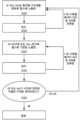
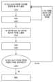
도 2a 내지 도 2c는 특정한 개시된 실시예들에 따른, 방법들에 대한 동작들을 도시하는 프로세스 흐름도이다.
도 3은 특정한 개시된 실시예들에 따른, 막들을 증착하기 위한 방법들의 예시적인 사이클들을 도시하는 타이밍 시퀀스도이다.
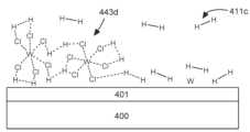
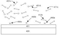
도 4a 내지 도 4j는 특정한 개시된 실시예들에 따른, 막들을 증착하기 위한 메커니즘의 일 예의 개략도들이다.
도 5는 H2/Ar/WClx/Ar 시퀀스 및 H2/Ar/n (WClx/Ar) 시퀀스를 사용하여 3-D NAND 구조체들의 텅스텐 충진을 비교하는 실험 결과들의 예시를 도시한다.
도 6은 특정한 개시된 실시예들을 수행하기 위한 예시적인 프로세스 툴의 개략도이다.
도 7은 특정한 개시된 실시예들을 수행하기 위한 예시적인 스테이션의 개략도이다.
도 8은 특정한 실시예들에 따라 사용될 수도 있는 매니폴드 시스템의 기본 피처들을 도시하는 개략도이다.Figure 1a is a schematic illustration of exemplary films on a substrate.
FIGS. 1B through 1J are schematic examples of various structures onto which tungsten or molybdenum may be deposited, according to certain disclosed embodiments.
FIGS. 2A through 2C are process flow diagrams illustrating operations for methods according to certain disclosed embodiments.
FIG. 3 is a timing sequence diagram illustrating exemplary cycles of methods for depositing films according to certain disclosed embodiments.
FIGS. 4A through 4J are schematic diagrams of examples of mechanisms for depositing films according to certain disclosed embodiments.
Figure 5 illustrates examples of experimental results comparing tungsten filling of 3-D NAND structures using H2 /Ar/WClx /Ar sequences and H2 /Ar/n (WClx /Ar) sequences.
FIG. 6 is a schematic diagram of an exemplary process tool for performing certain disclosed embodiments.
FIG. 7 is a schematic diagram of an exemplary station for performing certain disclosed embodiments.
FIG. 8 is a schematic diagram illustrating basic features of a manifold system that may be used according to certain embodiments.
이하의 기술 (description) 에서, 제시된 실시예들의 완전한 이해를 제공하기 위해 수많은 구체적 상세들이 제시되었다. 개시된 실시예들은 이들 구체적인 상세들 중 일부 또는 전부가 없이 실시될 수도 있다. 다른 예들에서, 공지된 프로세스 동작들은 개시된 실시예들을 불필요하게 모호하게 하지 않기 위해 상세히 기술되지 않았다. 개시된 실시예들이 구체적인 실시예들과 함께 기술될 것이지만, 이는 개시된 실시예들을 제한하는 것으로 의도되지 않았다는 것이 이해될 것이다.In the following description, numerous specific details have been set forth in order to provide a thorough understanding of the disclosed embodiments. The disclosed embodiments may be practiced without some or all of these specific details. In other instances, well-known process operations have not been described in detail so as not to unnecessarily obscure the disclosed embodiments. While the disclosed embodiments will be described in conjunction with the specific embodiments, it will be understood that this is not intended to limit the disclosed embodiments.
피처들의 텅스텐 (W) 충진은 전기적 콘택트들을 형성하기 위해 반도체 디바이스 제조에 자주 사용된다. 텅스텐 막들을 증착하는 종래의 방법들에서, 핵생성 텅스텐 층이 비아 또는 콘택트 내로 먼저 증착된다. 일반적으로, 핵생성 층은 그 위에 벌크 재료의 후속 형성을 용이하게 하도록 역할하는 박형의 컨포멀한 (conformal) 층이다. 텅스텐 핵생성 층은 피처의 측벽들 및 하단부를 컨포멀하게 코팅하도록 증착될 수도 있다. 아래에 놓인 피처 하단부 및 측벽들에 컨폼하는 (conform) 것은 고 품질 증착을 지지하는데 중요할 수 있다. 핵생성 층들은 종종 원자 층 증착 (atomic layer deposition; ALD) 또는 펄싱된 핵생성 층 (pulsed nucleation layer; PNL) 방법들을 사용하여 증착된다.Tungsten (W) filling of features is frequently used in semiconductor device fabrication to form electrical contacts. In conventional methods of depositing tungsten films, a nucleation tungsten layer is first deposited into the via or contact. Typically, the nucleation layer is a thin, conformal layer that serves to facilitate subsequent formation of bulk material thereon. The tungsten nucleation layer may be deposited to conformally coat the sidewalls and bottom of the feature. Conformity to the underlying feature bottom and sidewalls can be important in supporting a high quality deposition. Nucleation layers are often deposited using atomic layer deposition (ALD) or pulsed nucleation layer (PNL) methods.
PNL 기법에서, 반응물질의 펄스들은 반응물질들 사이에 퍼지 가스의 펄스에 의해 반응 챔버로부터 순차적으로 주입되고 퍼지된다. 제 1 반응물질이 기판 상에 흡착될 수 있어, 다음 반응물질과 반응하는데 이용가능하다. 프로세스는 목표된 두께가 달성될 때까지 순환적 방식으로 반복된다. PNL 기법들은 ALD 기법들과 유사하다. PNL은 일반적으로 (1 Torr보다 큰) 보다 높은 동작 압력 범위 및 (사이클 당 1보다 큰 모노레이어 막 성장) 사이클 당 보다 높은 성장 레이트에 의해 ALD로부터 구별된다. PNL 증착 동안 챔버 압력은 약 1 Torr 내지 약 400 Torr의 범위일 수도 있다. 본 명세서에 제공된 기술 (description) 의 맥락에서, PNL은 반도체 기판 상의 반응을 위해 순차적으로 반응물질들을 부가하는 임의의 순환적 프로세스를 광범위하게 구현한다. 따라서, 이 개념은 종래에 ALD로 지칭된 기법들을 구현한다. 개시된 실시예들의 맥락에서, 화학적 기상 증착 (chemical vapor deposition; CVD) 은 반응물질들이 함께 증기-상 또는 표면 반응을 위해 반응기로 도입되는, 프로세스들을 구현한다. PNL 프로세스 및 ALD 프로세스는 CVD 프로세스들과 구별되고 그 반대도 된다.In a PNL technique, pulses of reactants are sequentially injected and purged from a reaction chamber by pulses of purge gas between the reactants. The first reactant may be adsorbed on the substrate and available to react with the next reactant. The process is repeated in a cyclical manner until the desired thickness is achieved. PNL techniques are similar to ALD techniques. PNL is generally distinguished from ALD by its higher operating pressure range (greater than 1 Torr) and higher growth rates per cycle (greater than 1 monolayer film growth per cycle). Chamber pressures during PNL deposition may range from about 1 Torr to about 400 Torr. In the context of the description provided herein, PNL broadly embodies any cyclical process of sequentially adding reactants for reaction on a semiconductor substrate. Accordingly, the concept embodies techniques conventionally referred to as ALD. In the context of the disclosed embodiments, chemical vapor deposition (CVD) embodies processes in which reactants are introduced into a reactor together for vapor-phase or surface reaction. PNL processes and ALD processes are distinguished from CVD processes and vice versa.
텅스텐 핵생성 층이 증착된 후, 벌크 텅스텐은 통상적으로 수소 (H2) 와 같은 환원제를 사용하여 텅스텐 헥사플루오라이드 (WF6) 를 환원함으로써 CVD 프로세스에 의해 증착된다. 벌크 텅스텐은 텅스텐 핵생성 층과 상이하다. 본 명세서에서 사용된 바와 같은 벌크 텅스텐은 피처의 적어도 약 50 %와 같은 피처의 대부분 또는 전부를 충진하도록 사용된 텅스텐을 지칭한다. 그 위에 벌크 재료의 후속 형성을 용이하게 하도록 역할하는 박형의 컨포멀한 막인 핵생성 층과 달리, 벌크 텅스텐은 전류를 반송하도록 사용된다. 이는 핵생성 막과 비교하여 보다 큰 입자 크기 및 보다 낮은 저항률로 특징화될 수도 있다. 다양한 실시예들에서, 벌크 텅스텐은 적어도 50 Å의 두께로 증착된 텅스텐이다.After the tungsten nucleation layer is deposited, bulk tungsten is deposited by a CVD process, typically by reducing tungsten hexafluoride (WF6 ) using a reducing agent, such as hydrogen (H2 ). Bulk tungsten is different from the tungsten nucleation layer. Bulk tungsten, as used herein, refers to tungsten used to fill most or all of a feature, such as at least about 50% of the feature. Unlike the nucleation layer, which is a thin, conformal film that serves to facilitate subsequent formation of bulk material thereon, the bulk tungsten is used to transport current. It may be characterized by a larger grain size and lower resistivity compared to the nucleation film. In various embodiments, the bulk tungsten is tungsten deposited to a thickness of at least 50 Å.
디바이스들이 보다 작은 기술 노드들로 스케일링되고 보다 복잡한 패터닝 구조체들이 사용되기 때문에, 텅스텐 충진에서 다양한 문제들이 있다. 종래의 텅스텐의 증착은 불소-함유 전구체 텅스텐 헥사플루오라이드 (WF6) 의 사용을 수반하였다. 그러나, WF6의 사용은 증착된 텅스텐 막 내로 불소의 어느 정도 통합을 발생시킨다. 불소의 존재는 인접한 컴포넌트들 내로 전자마이그레이션 (electromigration) 및/또는 불소 확산을 유발할 수 있고 콘택트들을 손상시킬 수 있어서, 디바이스의 성능을 저하시킨다. 일 과제는 증착된 텅스텐 막에서 불소 함량이 감소하는 것이다. 피처 사이즈가 감소됨에 따라 특정한 불소 농도의 효과는 상승한다. 이는 보다 박형의 막들이 보다 박형의 막들을 통해 확산하기 보다 쉬운 증착된 텅스텐 막의 불소와 함께 보다 작은 피처들 내에 증착되기 때문이다.As devices scale to smaller technology nodes and more complex patterning structures are used, tungsten fill presents a number of challenges. Conventional tungsten deposition has involved the use of the fluorine-containing precursor tungsten hexafluoride (WF6 ). However, the use of WF6 results in some degree of fluorine incorporation into the deposited tungsten film. The presence of fluorine can cause electromigration and/or fluorine diffusion into adjacent components and can damage contacts, thereby degrading device performance. One challenge is to reduce the fluorine content in the deposited tungsten film. As feature size decreases, the effectiveness of a given fluorine concentration increases. This is because thinner films are deposited into smaller features, with fluorine in the deposited tungsten film more readily diffusing through the thinner films.
불소 확산을 방지하는 일 방법은 텅스텐으로부터 옥사이드 층과 같은 기판의 다른 층들로 불소가 확산하는 것을 방지하도록 텅스텐을 증착하기 전 하나 이상의 배리어 층들을 증착하는 단계를 포함한다. 예를 들어, 도 1a는 기판 상에 증착된 층들의 예시적인 스택을 도시한다. 기판 (190) 은 실리콘 층 (192), 옥사이드 층 (194) (예를 들어, 티타늄 옥사이드 (TiOx), 테트라에틸 오소실리케이트 (TEOS) 옥사이드, 등), 배리어 층 (196) (예를 들어, 티타늄 나이트라이드 (TiN)), 텅스텐 핵생성 층 (198), 및 벌크 텅스텐 층 (199) 을 포함한다. 배리어 층 (196) 은 벌크 텅스텐 층 (199) 및 텅스텐 핵생성 층 (198) 으로부터 옥사이드 층으로 불소 확산을 방지하도록 증착된다. 그러나, 디바이스들이 축소됨에 따라, 배리어 층들은 보다 박형이 되고, 불소는 여전히 증착된 텅스텐 층들로부터 확산할 수도 있다. 보다 고온에서 수행된 벌크 텅스텐의 화학적 기상 증착이 보다 낮은 불소 함량을 발생시키지만, 이러한 막들은 불량한 단차 커버리지 (step coverage) 를 가질 수도 있다.A method of preventing fluorine diffusion includes depositing one or more barrier layers prior to depositing tungsten to prevent fluorine from diffusing from the tungsten to other layers of the substrate, such as an oxide layer. For example, FIG. 1A illustrates an exemplary stack of layers deposited on a substrate. The substrate (190) includes a silicon layer (192), an oxide layer (194) (e.g., titanium oxide (TiOx ), tetraethyl orthosilicate (TEOS) oxide, etc.), a barrier layer (196) (e.g., titanium nitride (TiN)), a tungsten nucleation layer (198), and a bulk tungsten layer (199). The barrier layer (196) is deposited to prevent fluorine diffusion from the bulk tungsten layer (199) and the tungsten nucleation layer (198) to the oxide layer. However, as devices shrink, the barrier layers become thinner, and fluorine may still diffuse from the deposited tungsten layers. Although chemical vapor deposition of bulk tungsten performed at higher temperatures produces lower fluorine content, these films may have poor step coverage.
또 다른 과제는 증착된 막들 상의 응력이 감소하는 것이다. 보다 박형의 텅스텐 막들은 상승된 인장 응력을 갖는 경향이 있다. CVD에 의해 벌크 텅스텐 막들을 증착하기 위한 종래의 기법들은 200 Å 막에 대해 2.5 GPa보다 큰 인장 응력을 갖는다. 고 열적 인장 응력은 기판으로 하여금 말리게 (curl) 하고, 이는 후속 프로세싱을 어렵게 한다. 예를 들어, 후속 프로세스들은 챔버에서 프로세스들을 수행하기 위해 화학적 기계적 평탄화, 재료들의 증착, 및/또는 기판 홀더로 기판의 클램핑을 포함할 수도 있다. 그러나, 이들 프로세스들은 종종 편평한 기판에 의존하고, 말린 기판은 불균일한 프로세싱 또는 기판 프로세싱 불능을 발생시킨다. 어닐링과 같이 다른 재료들의 막들의 응력을 감소시키기 위한 기존 방법들이 있지만, 텅스텐은 고 융점으로 인해 한번 증착되면 입자들로 하여금 이동되거나 변경되게 하는 표면 이동성을 갖지 않는다.Another challenge is reducing stress on the deposited films. Thinner tungsten films tend to have elevated tensile stresses. Conventional techniques for depositing bulk tungsten films by CVD have tensile stresses greater than 2.5 GPa for a 200 Å film. High thermal tensile stresses cause the substrate to curl, making subsequent processing difficult. For example, subsequent processes may include chemical mechanical planarization, deposition of materials, and/or clamping the substrate to a substrate holder to perform processes in a chamber. However, these processes often rely on flat substrates, and a curled substrate results in non-uniform processing or inability to process the substrate. There are conventional methods for reducing stress on films of other materials, such as annealing, but tungsten, due to its high melting point, does not have surface mobility that allows particles to move or change once deposited.
불소-프리 텅스텐 (FFW) 전구체들이 이러한 신뢰성 및 통합 문제들 또는 디바이스 성능 문제들을 방지하는데 유용하다. 현재 FFW 전구체들은 금속 유기 전구체들을 포함하지만, 금속 유기 전구체들로부터 탄소, 수소, 질소, 및 산소와 같은 원소들의 바람직하지 않은 추적들이 텅스텐 막에도 통합될 수도 있다. 일부 금속 유기 불소-프리 전구체들은 또한 텅스텐 증착 프로세스들로 용이하게 구현 또는 통합되지 않는다.Fluorine-free tungsten (FFW) precursors are useful for avoiding these reliability and integration issues or device performance problems. Current FFW precursors include metalorganic precursors, but undesirable traces of elements such as carbon, hydrogen, nitrogen, and oxygen from the metalorganic precursors may also be incorporated into the tungsten film. Some metalorganic fluorine-free precursors are also not easily implemented or integrated into tungsten deposition processes.
본 명세서에 기술된 일부 구현예들은 텅스텐 클로라이드 (WClx) 전구체를 사용한 텅스텐의 증착과 관련한다. 텅스텐 클로라이드는 텅스텐 펜타클로라이드 (WCl5), 텅스텐 헥사클로라이드 (WCl6), 텅스텐 테트라클로라이드 (WCl4), 텅스텐 디클로라이드 (WCl2), 및 이들의 혼합물들을 포함한다. 본 명세서의 예들이 예들로서 WCl5 및 WCl6를 참조하지만, 다른 텅스텐 클로라이드들이 개시된 실시예들과 함께 사용될 수도 있다는 것이 이해된다. 특정한 개시된 실시예들을 사용하여 증착된 막들은 불소-프리이다. 특정한 개시된 실시예들은 염소-함유 텅스텐 전구체 및 수소의 교번하는 펄스들을 사용하여 벌크 텅스텐을 증착하는 것으로 지향된다.Certain embodiments described herein relate to the deposition of tungsten using a tungsten chloride (WClx ) precursor. Tungsten chlorides include tungsten pentachloride (WCl5 ), tungsten hexachloride (WCl6 ), tungsten tetrachloride (WCl4 ), tungsten dichloride (WCl2 ), and mixtures thereof. While the embodiments herein reference WCl5 and WCl6 as examples, it is understood that other tungsten chlorides may be used with the disclosed embodiments. Films deposited using certain disclosed embodiments are fluorine-free. Certain disclosed embodiments are directed to depositing bulk tungsten using alternating pulses of a chlorine-containing tungsten precursor and hydrogen.
WCl5 및 WCl6에 의한 증착은 텅스텐 클로라이드들에 의해 가능한 에칭으로 인해 WF6와 함께 존재하지 않는 과제들을 제공한다. 텅스텐 클로라이드들은 보다 적은 반응성이고, 그 결과, 증착은 WF6를 사용한 증착보다 높은 온도에서 수행된다. 증발된 WCl6는 텅스텐 증착 챔버 내로 반송하는 것을 인에이블하도록 충분히 높은 증기압을 갖는다. 그러나, WCl6 는 WCl5보다 기판을 에칭할 가능성이 높을 수도 있다. WCl5가 기판을 에칭할 가능성이 보다 낮지만, WCl5는 또한 WCl6보다 높은 증기압을 갖는다. 보다 낮은 증기압이 저 저항률을 갖는 텅스텐 막들을 증착하는데 유용하지만, 일부 증착 동작들은 불량한 단차 커버리지를 가질 수도 있다.Depositions with WCl5 and WCl6 present challenges that are not present with WF6 due to possible etching by the tungsten chlorides. The tungsten chlorides are less reactive and, as a result, the deposition is performed at higher temperatures than deposition using WF6 . The evaporated WCl6 has a sufficiently high vapor pressure to enable its transport into the tungsten deposition chamber. However, WCl6 may be more likely to etch the substrate than WCl5 . Although WCl5 is less likely to etch the substrate, WCl5 also has a higher vapor pressure than WCl6 . While the lower vapor pressure is useful for depositing low resistivity tungsten films, some deposition operations may have poor step coverage.
본 명세서에 기술된 방법들은 몰리브덴 클로라이드 또는 몰리브덴 옥시클로라이드 전구체들에 의한 몰리브덴 (Mo) 의 증착을 위해 또한 사용될 수도 있다. 몰리브덴은 저 저항 금속화 스택 구조체들을 형성하도록 사용될 수도 있고 텅스텐의 자리를 취할 수도 있다.The methods described herein may also be used for the deposition of molybdenum (Mo) from molybdenum chloride or molybdenum oxychloride precursors. Molybdenum may be used to form low-resistivity metallization stack structures and may take the place of tungsten.
개시된 실시예들은 광범위한 다양한 적용예들을 갖는다. 방법들은 고 단차 커버리지를 갖는 피처들 내로 텅스텐 또는 몰리브덴을 증착하도록 사용될 수도 있고, 3D NAND 구조체들 내로 텅스텐을 증착하도록 또한 사용될 수도 있다.The disclosed embodiments have a wide variety of applications. The methods may be used to deposit tungsten or molybdenum into features having high step coverage, and may also be used to deposit tungsten into 3D NAND structures.
본 명세서에 기술된 방법들은 챔버에 하우징될 수도 있는 기판 상에서 수행된다. 기판은 유전체, 도전 또는 반도전 재료와 같은 재료의 하나 이상의 층들이 그 위에 증착된 웨이퍼들을 포함하는, 실리콘 또는 다른 반도체 웨이퍼, 예를 들어, 200-㎜ 웨이퍼, 300-㎜ 웨이퍼, 또는 450-㎜ 웨이퍼일 수도 있다. 방법들은 반도체 기판들로 제한되지 않고, 텅스텐과 같은 금속으로 임의의 피처를 충진하도록 수행될 수도 있다.The methods described herein are performed on a substrate that may be housed in a chamber. The substrate may be a silicon or other semiconductor wafer, for example, a 200-mm wafer, a 300-mm wafer, or a 450-mm wafer, having one or more layers of a material, such as a dielectric, conductive or semiconductive material, deposited thereon. The methods are not limited to semiconductor substrates, and may be performed to fill any feature with a metal, such as tungsten.
기판들은 좁은 그리고/또는 재차 들어간 (re-entrant) 개구부들, 피처 내 협폭부들 (constrictions), 및 고 종횡비들 중 하나 이상을 특징으로 할 수도 있는, 비아 또는 콘택트 홀들과 같은 피처들을 가질 수도 있다. 피처가 상기 기술된 층들 중 하나 이상에 형성될 수도 있다. 예를 들어, 피처는 유전체 층에 적어도 부분적으로 형성될 수도 있다. 일부 실시예들에서, 피처는 적어도 약 2:1, 적어도 약 4:1, 적어도 약 6:1, 적어도 약 10:1, 적어도 약 25:1, 이상의 종횡비를 가질 수도 있다. 피처의 일 예는 반도체 기판 또는 기판 상의 층 내의 홀 또는 비아이다.The substrates may have features, such as vias or contact holes, which may be characterized by one or more of narrow and/or re-entrant openings, constrictions within the feature, and high aspect ratios. The feature may be formed in one or more of the layers described above. For example, the feature may be formed at least partially in a dielectric layer. In some embodiments, the feature may have an aspect ratio of at least about 2:1, at least about 4:1, at least about 6:1, at least about 10:1, at least about 25:1, or more. An example of a feature is a hole or via in a semiconductor substrate or a layer on the substrate.
도 1b 내지 도 1h는 개시된 실시예들에 따른, 금속이 증착될 수도 있는 다양한 구조체들의 개략적인 예들이다. 도 1b는 텅스텐 또는 몰리브덴과 같은 금속으로 충진될 수직 피처 (101) 의 단면도의 일 예를 도시한다. 피처는 기판 (103) 내에 피처 홀 (105) 을 포함할 수 있다. 홀 (105) 또는 다른 피처는 개구부 근방 치수, 예를 들어, 약 10 ㎚ 내지 500 ㎚, 예를 들어 약 25 ㎚ 내지 약 300 ㎚의 개구부 직경 또는 라인 폭을 가질 수도 있다. 피처 홀 (105) 은 충진되지 않은 피처 또는 단순히 피처로 지칭될 수 있다. 피처 (101), 및 임의의 피처가 수직 축들을 갖는 수직으로 배향된 피처들 및 수평 축들을 갖는 수평으로 배향된 피처들을 갖는 피처의 길이를 통해 연장하는 축 (118) 에 의해 부분적으로 특징화될 수도 있다.FIGS. 1B-1H are schematic examples of various structures into which metal may be deposited, according to the disclosed embodiments. FIG. 1B illustrates an example of a cross-sectional view of a vertical feature (101) to be filled with a metal, such as tungsten or molybdenum. The feature may include a feature hole (105) in a substrate (103). The hole (105) or other feature may have an opening diameter or line width of about 10 nm to 500 nm, for example about 25 nm to about 300 nm, around the opening. The feature hole (105) may be referred to as an unfilled feature or simply a feature. A feature (101), and any feature may be characterized in part by an axis (118) extending through the length of the feature having vertically oriented features having vertical axes and horizontally oriented features having horizontal axes.
일부 실시예들에서, 피처들은 3D NAND 구조체의 워드라인 피처들이다. 예를 들어, 기판이 적어도 200 Å 깊이의 수직 채널들을 갖는 임의의 수의 워드라인들 (예를 들어, 50 내지 150) 을 갖는 워드라인 구조체를 포함할 수도 있다. 또 다른 예는 기판 또는 층의 트렌치이다. 피처들은 임의의 깊이일 수도 있다. 다양한 실시예들에서, 피처는 배리어 층 또는 접착 층과 같은, 하부 층을 가질 수도 있다. 하부 층들의 비제한적인 예들은 유전체 층들 및 도전 층들, 예를 들어, 실리콘 옥사이드들, 실리콘 나이트라이드들, 실리콘 카바이드들, 금속 옥사이드들, 금속 나이트라이드들, 금속 카바이드들, 및 금속 층들을 포함한다.In some embodiments, the features are wordline features of the 3D NAND structure. For example, the substrate may include a wordline structure having any number of wordlines (e.g., 50 to 150) having vertical channels at least 200 Å deep. Another example is a trench in the substrate or layer. The features may be of any depth. In various embodiments, the feature may have a sublayer, such as a barrier layer or an adhesion layer. Non-limiting examples of sublayers include dielectric layers and conductive layers, such as silicon oxides, silicon nitrides, silicon carbides, metal oxides, metal nitrides, metal carbides, and metal layers.
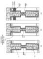
도 1c는 재차 들어간 프로파일을 갖는 피처 (101) 의 일 예를 도시한다. 재차 들어간 프로파일은 피처의 하단부, 폐쇄된 단부, 또는 내부로부터 피처 개구부로 좁아지는 프로파일이다. 다양한 구현예들에 따라, 프로파일은 점진적으로 좁아질 수도 있고 그리고/또는 피처 개구부에서 오버행 (overhang) 을 포함할 수도 있다. 도 1c는 피처 홀 (105) 의 측벽 또는 내부 표면들을 라이닝하는 하부 층 (113) 을 갖는, 후자의 예를 도시한다. 하부 층 (113) 은 예를 들어, 확산 배리어 층, 접착 층, 핵생성 층, 이의 조합, 또는 임의의 다른 적용가능한 재료일 수 있다. 하부 층들의 비제한적인 예들은 유전체 층들 및 도전 층들, 예를 들어, 실리콘 옥사이드들, 실리콘 나이트라이드들, 실리콘 카바이드들, 금속 옥사이드들, 금속 나이트라이드들, 금속 카바이드들, 및 금속 층들을 포함할 수 있다. 특정한 구현예들에서 하부 층은 티타늄, 티타늄 나이트라이드, 텅스텐 나이트라이드, 티타늄 알루미나이드, 텅스텐, 및 몰리브덴 중 하나 이상일 수 있다. 일부 실시예들에서, 하부 층은 텅스텐-프리이다. 일부 실시예들에서, 하부 층은 몰리브덴-프리이다. 하부 층 (113) 은 하부 층 (113) 이 피처 (101) 내부보다 피처 (101) 의 개구부에서 보다 두껍도록 오버행 (115) 을 형성한다.FIG. 1c illustrates an example of a feature (101) having a re-entrant profile. A re-entrant profile is a profile that tapers from the bottom, closed end, or interior of the feature into a feature opening. According to various implementations, the profile may be gradually tapered and/or may include an overhang at the feature opening. FIG. 1c illustrates the latter example, having an underlayer (113) lining the sidewalls or interior surfaces of the feature hole (105). The underlayer (113) can be, for example, a diffusion barrier layer, an adhesion layer, a nucleation layer, a combination thereof, or any other applicable material. Non-limiting examples of underlayers can include dielectric layers and conductive layers, for example, silicon oxides, silicon nitrides, silicon carbides, metal oxides, metal nitrides, metal carbides, and metal layers. In certain embodiments, the sublayer can be one or more of titanium, titanium nitride, tungsten nitride, titanium aluminide, tungsten, and molybdenum. In some embodiments, the sublayer is tungsten-free. In some embodiments, the sublayer is molybdenum-free. The sublayer (113) forms an overhang (115) such that the sublayer (113) is thicker at the opening of the feature (101) than inside the feature (101).
일부 구현예들에서, 피처 내부에 하나 이상의 협폭부들을 갖는 피처들이 충진될 수도 있다. 도 1d는 협폭부들을 갖는 다양한 충진된 피처들의 도면들의 예들을 도시한다. 도 1d의 예들 (a), (b) 및 (c) 각각은 피처 내 중간지점에 협폭부들 (109) 을 포함한다. 협폭부들 (109) 은 예를 들어, 약 15 ㎚ 내지 20 ㎚ 넓이일 수 있다. 협폭부들은 종래의 기법들을 사용하여 피처 내 텅스텐 또는 몰리브덴의 증착 동안 핀치 오프 (pinch off) 를 유발할 수 있고, 추가 증착을 차단하는 증착된 금속이 피처의 일부가 충진되기 전 협폭부를 넘어가 (past), 피처 내 보이드들을 발생시킨다. 예 (b) 는 피처 개구부에서 라이너/배리어 오버행 (115) 을 더 포함한다. 이러한 오버행은 잠재적인 핀치 오프 지점일 수 있다. 예 (c) 는 예 (b) 의 오버행 (115) 보다 필드 영역으로부터 더 먼 협폭부 (112) 를 포함한다.In some implementations, features may be filled having one or more narrow sections within the feature. FIG. 1d illustrates examples of drawings of various filled features having narrow sections. Examples (a), (b), and (c) of FIG. 1d each include narrow sections (109) at a midpoint within the feature. The narrow sections (109) can be, for example, about 15 nm to 20 nm wide. The narrow sections can cause pinch off during deposition of tungsten or molybdenum within the feature using conventional techniques, causing the deposited metal, which blocks further deposition, to pass through the narrow sections before a portion of the feature is filled, creating voids within the feature. Example (b) further includes a liner/barrier overhang (115) at the feature opening. This overhang can be a potential pinch off point. Example (c) includes a narrow portion (112) further from the field area than the overhang (115) of example (b).
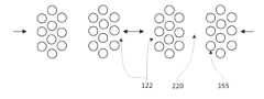
3-D 메모리 구조체들 내와 같이, 수평 피처들이 또한 충진될 수 있다. 도 1e는 협폭부 (151) 를 포함하는 수평 피처 (150) 의 일 예를 도시한다. 예를 들어, 수평 피처 (150) 는 3D NAND 구조체의 워드라인일 수도 있다. 일부 구현예들에서, 협폭부들은 3D NAND 또는 다른 구조체의 필라들 (pillars) 의 존재로 인한 것일 수 있다. 예를 들어, 도 1f는 VNAND 스택들 (좌측 (125) 및 우측 (126)), 중앙 수직 구조체 (130), 및 중앙 수직 구조체 (130) 의 마주보는 측벽들 (140) 상의 개구부들 (122) 을 갖는 복수의 스택된 수평 피처들 (120) 을 갖는 3-D NAND (또한 수직 NAND 또는 VNAND로 지칭됨) 구조체 (110) (반도체 기판 (103) 상에 형성된) 의 측단면도를 제공한다. 도 1f는 함께 "트렌치-유사 (trench-like)" 중앙 수직 구조체 (130) 를 형성하는 표현된 3-D NAND 구조체 (110) 의 2 개의 "스택들"을 디스플레이하지만, 특정한 실시예들에서, 차례로 배치되고 서로 공간적으로 평행하게 진행하는 3 개 이상의 "스택들"이, 도 1f에 명시적으로 예시된 것과 같은, 중앙 수직 구조체 (130) 를 형성하는 인접한 "스택들"의 쌍 각각 사이의 갭이 있을 수도 있다는 것을 주의하라. 이 실시예에서, 수평 피처들 (120) 은 개구부들 (122) 을 통해 중앙 수직 구조체 (130) 로부터 유체적으로 액세스가능한 3-D 메모리 워드라인 피처들이다. 도면에 명시적으로 나타나지 않지만, 도 1f에 도시된 3-D NAND 스택들 (125 및 126) 모두 (즉, 좌측 3-D NAND 스택 (125) 및 우측 3-D NAND 스택 (126)) 에 존재하는 수평 피처들 (120) 은 또한 스택들 (각각 극좌측 및 극우측) 의 다른 측면들로부터 부가적인 3-D NAND 스택들 (극좌측 및 극우측으로, 미도시) 에 의해 형성된 유사한 수직 구조체들을 통해 액세스가능하다. 달리 말하면, 3-D NAND 스택 (125, 126) 각각은 중앙 수직 구조체 (130) 를 통해 3-D NAND 스택의 양 측면들로부터 유체적으로 액세스가능한 워드라인 피처들의 스택을 포함한다. 도 1f에 개략적으로 예시된 특정한 예에서, 3-D NAND 스택 각각은 6 쌍의 스택된 워드라인들을 포함하지만, 다른 실시예들에서, 3-D NAND 메모리 레이아웃은 임의의 수의 수직으로 스택된 쌍들의 워드라인들을 포함할 수도 있다.As with 3-D memory structures, horizontal features may also be filled. FIG. 1e illustrates an example of a horizontal feature (150) including a narrow portion (151). For example, the horizontal feature (150) may be a word line of a 3D NAND structure. In some implementations, the narrow portions may be due to the presence of pillars in the 3D NAND or other structure. For example, FIG. 1f provides a cross-sectional side view of a 3-D NAND (also referred to as vertical NAND or VNAND) structure (110) (formed on a semiconductor substrate (103)) having VNAND stacks (left (125) and right (126)), a central vertical structure (130), and a plurality of stacked horizontal features (120) having openings (122) on opposing sidewalls (140) of the central vertical structure (130). Although FIG. 1f displays two "stacks" of the depicted 3-D NAND structure (110) that together form a "trench-like" central vertical structure (130), note that in certain embodiments, there may be three or more "stacks" arranged one behind the other and running spatially parallel to one another, with a gap between each pair of adjacent "stacks" forming a central vertical structure (130), such as explicitly illustrated in FIG. 1f. In this embodiment, the horizontal features (120) are 3-D memory wordline features that are fluidly accessible from the central vertical structure (130) through openings (122). Although not explicitly shown in the drawings, the horizontal features (120) present in both of the 3-D NAND stacks (125 and 126) illustrated in FIG. 1f (i.e., the left 3-D NAND stack (125) and the right 3-D NAND stack (126)) are also accessible from other sides of the stacks (extremely left and extreme right, respectively) via similar vertical structures formed by additional 3-D NAND stacks (extremely left and extreme right, not shown). In other words, each of the 3-D NAND stacks (125, 126) includes a stack of wordline features that are fluidically accessible from both sides of the 3-D NAND stack via a central vertical structure (130). In the specific example schematically illustrated in FIG. 1f, each of the 3-D NAND stacks includes six pairs of stacked wordlines, although in other embodiments, the 3-D NAND memory layout may include any number of vertically stacked pairs of wordlines.
3-D NAND 스택의 워드라인 피처들은 통상적으로 실리콘 옥사이드 층 및 실리콘 나이트라이드 층의 교번하는 스택을 증착하고, 이어서 사이에 갭들을 갖는 옥사이드들 층들의 스택을 남기면서 나이트라이드 층들을 선택적으로 제거함으로써 형성된다. 이들 갭들은 워드라인 피처들이다. 임의의 수의 워드라인들이 이들을 형성하는데 이용가능한 기법, 뿐만 아니라 수직 피처들의 (실질적으로) 보이드-프리 충진들을 성공적으로 달성하도록 이용가능한 기법이 있는 한, 이러한 3-D NAND 구조체에 수직으로 스택될 수도 있다. 따라서, 예를 들어, VNAND 스택이 2 내지 256 개의 수평 워드라인 피처들, 또는 8 내지 128 개의 수평 워드라인 피처들, 또는 16 내지 64 개의 수평 워드라인 피처들, 등을 포함할 수도 있다 (열거된 범위들은 언급된 엔드포인트들을 포함하는 것으로 이해됨).The wordline features of a 3-D NAND stack are typically formed by depositing alternating stacks of silicon oxide layers and silicon nitride layers, and then selectively removing the nitride layers, leaving a stack of oxide layers with gaps therebetween. These gaps are the wordline features. Any number of wordlines may be stacked vertically in such a 3-D NAND structure, as long as there is a technique available to form them, as well as a technique available to successfully achieve (substantially) void-free fill of the vertical features. Thus, for example, a VNAND stack may include 2 to 256 horizontal wordline features, or 8 to 128 horizontal wordline features, or 16 to 64 horizontal wordline features, etc. (the enumerated ranges being understood to be inclusive of the noted endpoints).
도 1g는 도 1f의 측면에 도시된 동일한 3-D NAND 구조체 (110) 의 단면 톱-다운 (top-down) 도를 도 1f의 점선 수평 라인으로 나타낸 바와 같은 수평 섹션 (160) 을 통해 취해진 단면과 함께 제공한다. 도 1g의 단면도는 반도체 기판 (103) 의 베이스 (base) 로부터 3-D NAND 스택 (110) 의 상단부로 수직으로 진행하는 것으로 도 1f에 도시된 몇몇 행들의 필라들 (155) 을 예시한다. 일부 실시예들에서, 이들 필라들 (155) 은 폴리실리콘 재료로부터 형성되고 3-D NAND 구조체 (110) 에 구조적으로 그리고 기능적으로 중요하다. 일부 실시예들에서, 이러한 폴리실리콘 필라들이 필라들 내에 형성된 스택된 메모리 셀들에 대해 게이트 전극들로서 역할을 할 수도 있다. 도 1g의 상면도는 필라들 (155) 이 워드라인 피처들 (120) 로 개구부들 (122) 내에 협폭부들을 형성한다는 것을 예시한다 - 즉 중앙 수직 구조체 (130) 로부터 개구부들 (122) (도 1g의 화살표들로 나타낸 바와 같이) 을 통한 워드라인 피처들 (120) 의 유체 액세스가능성이 필라들 (155) 에 의해 억제된다. 일부 실시예들에서, 인접한 폴리실리콘 필라들 사이의 수평 갭의 사이즈는 약 1 내지 20 ㎚이다. 이 유체 액세스가능성의 감소는 텅스텐 재료로 워드라인 피처들 (120) 을 균일하게 충진하는 것의 어려움을 증가시킨다. 워드라인 피처들 (1) 의 구조체 및 필라들 (155) 의 존재로 인한 텅스텐 재료 또는 몰리브덴 재료로 이들을 균일하게 충진하는 것의 어려움은 도 1h, 도 1i 및 도 1j에 더 예시된다.FIG. 1g provides a cross-sectional top-down view of the same 3-D NAND structure (110) illustrated in FIG. 1f along with a cross-section taken through a horizontal section (160) as indicated by the dashed horizontal line in FIG. 1f. The cross-sectional view of FIG. 1g illustrates several rows of pillars (155) as illustrated in FIG. 1f running vertically from the base of the semiconductor substrate (103) to the top of the 3-D NAND stack (110). In some embodiments, these pillars (155) are formed from a polysilicon material and are structurally and functionally significant to the 3-D NAND structure (110). In some embodiments, these polysilicon pillars may also serve as gate electrodes for stacked memory cells formed within the pillars. The top view of FIG. 1g illustrates that the pillars (155) form narrow gaps within the openings (122) into the wordline features (120)—i.e., the fluid accessibility of the wordline features (120) through the openings (122) (as indicated by the arrows in FIG. 1g) from the central vertical structure (130) is inhibited by the pillars (155). In some embodiments, the size of the horizontal gap between adjacent polysilicon pillars is about 1 to 20 nm. This reduction in fluid accessibility increases the difficulty of uniformly filling the wordline features (120) with tungsten material. The difficulty in uniformly filling the structure of the wordline features (1) with tungsten material or molybdenum material due to the presence of pillars (155) is further illustrated in FIGS. 1h, 1i and 1j.
도 1h는 도 1f에 도시된 것과 유사하지만, 이 도면에서는 단일 쌍의 워드라인 피처들 (120) 에 포커싱하고, 부가적으로 충진된 워드라인 피처들 (120) 의 보이드 (175) 의 형성을 발생시키는, 금속 충진 프로세스를 개략적으로 예시하는, 수직으로 절단된 (cut through) 3-D NAND 구조체를 나타낸다. 도 1i는 또한 보이드 (175) 를 개략적으로 예시하지만, 이 도면에서 도 1g에 나타낸 수평 절단도와 유사한, 수평 절단 필라들 (155) 을 통해 예시된다. 도 1j는 협폭부 형성 필라들 (155) 주변에 텅스텐 또는 몰리브덴 재료의 축적을 예시하고, 축적은 부가적인 텅스텐 또는 몰리브덴 재료가 보이드들 (175) 의 영역 내에 증착될 수 없도록 개구부들 (122) 의 핀치 오프를 발생시킨다. 보이드-프리 텅스텐 또는 몰리브덴 충진이 개구부들 (122) 의 핀치 오프를 유발하고 워드라인 피처들 (120) 내로 추가 전구체 마이그레이션을 방지하는, 필라들 (155) 주변 텅스텐의 축적된 증착 전에, 수직 구조체 (130) 를 통해, 개구부들 (122) 을 통해, 협폭 필라들 (155) 을 넘어, 워드라인 피처들 (120) 의 가장 먼 범위까지 아래로 충분한 양의 증착 전구체의 마이그레이션에 의존한다는 것이 도 1h 및 도 1i로부터 자명하다. 유사하게, 도 1j는 위에서 단면으로 본 단일 워드라인 피처 (120) 를 나타내고, 상당한 폭의 필라들 (155) 이 그렇지 않으면 워드라인 피처 (120) 를 통한 개방 경로일 수 있는 워드라인 피처 (120) 를 부분적으로 차단, 그리고/또는 좁히고 (narrow), 그리고/또는 협폭화하도록 작용한다는 사실로 인해, 대체로 컨포멀한 텅스텐 또는 몰리브덴 재료의 증착이 워드라인 피처 (120) 의 내부를 핀치 오프하기 시작하는 지 예시한다. (도 1j의 예는 도 1i에 도시된 필라 협폭부들의 구조체의 3-D 피처들의 2-D 렌더링으로 이해될 수 있어서, 단면도가 아니라 평면도에서 볼 수 있는 협폭부들을 예시한다는 것이 이해되어야 한다.)FIG. 1h shows a vertically cut through 3-D NAND structure, similar to that illustrated in FIG. 1f , but in this figure focuses on a single pair of wordline features (120) and schematically illustrates a metal filling process that causes the formation of voids (175) in the additionally filled wordline features (120). FIG. 1i also schematically illustrates the voids (175), but in this figure through horizontal cut pillars (155), similar to the horizontal cut through illustrated in FIG. 1g . FIG. 1j illustrates the accumulation of tungsten or molybdenum material around the narrow-section forming pillars (155), the accumulation causing pinch off of the openings (122) such that additional tungsten or molybdenum material cannot be deposited within the region of the voids (175). It is evident from FIGS. 1h and 1i that the void-free tungsten or molybdenum fill relies on the migration of sufficient amounts of the deposition precursor down through the vertical structures (130), through the openings (122), beyond the narrow pillars (155), and into the farthest extent of the wordline features (120) prior to the accumulated deposition of tungsten around the pillars (155) to cause pinch off of the openings (122) and prevent further precursor migration into the wordline features (120). Similarly, FIG. 1j illustrates a single wordline feature (120) in cross-section from above, and illustrates how the deposition of a generally conformal tungsten or molybdenum material begins to pinch off the interior of the wordline feature (120) due to the fact that the substantially wide pillars (155) act to partially block, narrow, and/or narrow what would otherwise be an open path through the wordline feature (120). (It should be understood that the example of FIG. 1j is a 2-D rendering of the 3-D features of the structure of the pillar narrows depicted in FIG. 1i, and thus illustrates the narrows as seen in a plan view rather than a cross-section.)
3D 구조체들이 최내측 영역 및 최하측 영역으로 하여금 충진되게 하도록 전구체들로 보다 길고 그리고/또는 보다 집중된 노출을 필요로 할 수도 있다. 3D 구조체들은 WClx 전구체들을 채용할 때 구조체의 부분들로서 보다 많은 에칭을 허용하는 보다 길고 보다 집중된 노출과 함께, 이들의 에칭 성향으로 인해, 특히 어려울 수 있다. 이들 과제들은 또한 몰리브덴 클로라이드 전구체들을 사용해도 존재할 수도 있다.3D structures may require longer and/or more focused exposures to the precursors to allow for filling of the innermost and lowermost regions. 3D structures can be particularly challenging when employing WClx precursors due to their etching propensity, with longer and more focused exposures allowing more etching of portions of the structure. These challenges may also exist with molybdenum chloride precursors.
수평으로 배향된 및 수직으로 배향된 피처들에 대한 피처 충진의 예들은 이하에 기술된다. 대부분의 경우, 이 예들은 수평으로 배향된 또는 수직으로 배향된 피처들 모두에 적용가능하다는 것을 주의해야 한다. 게다가, 이하의 기술에서, 용어 "측방향 (lateral)"은 피처 축에 일반적으로 직교하는 방향을 지칭하고 용어 "수직 (vertical)"은 일반적으로 피처 축을 따른 방향을 지칭하도록 사용될 수도 있다는 것을 또한 주의해야 한다.Examples of feature filling for horizontally oriented and vertically oriented features are described below. It should be noted that in most cases, these examples are applicable to both horizontally oriented or vertically oriented features. Additionally, it should also be noted that in the description below, the term "lateral" may be used to refer to a direction generally orthogonal to a feature axis, and the term "vertical" may be used to refer to a direction generally along a feature axis.
다양한 실시예들에 따라, 이하에 기술된 방법들은 ALD 사이클의 복수의 환원제/퍼지 사이클들 및/또는 복수의 금속-전구체/퍼지 사이클들에 구조체를 노출하는 것을 수반한다. 일부 구현예들에서, 다음의 장점들 중 하나 이상이 달성될 수도 있다. 일부 실시예들에서, 퍼지 가스 펄싱과 함께 배치된 복수의 텅스텐-함유 전구체 도즈들 (예를 들어, W/Ar/W/Ar/W/Ar/W/Ar, W는 텅스텐-함유 전구체의 펄스이고 Ar은 아르곤 퍼지 가스의 펄스를 나타냄) 은 3-D NAND 워드라인 구조체 내로 깊이 텅스텐-함유 전구체의 전달을 인에이블하거나 구조체로 충진하는 것을 어렵게 한다. 일부 구현예들에서, 다음의 장점들 중 하나 이상이 달성될 수도 있다. 일부 실시예들에서, 퍼지 가스 펄싱과 함께 배치된 복수의 몰리브덴-함유 전구체 도즈들 (예를 들어, Mo/Ar/Mo/Ar/Mo/Ar/Mo/Ar, Mo는 몰리브덴-함유 전구체의 펄스이고 Ar은 아르곤 퍼지 가스의 펄스를 나타냄) 은 3-D NAND 워드라인 구조체 내로 깊이 몰리브덴-함유 전구체의 전달을 인에이블하거나 구조체로 충진하는 것을 어렵게한다.According to various embodiments, the methods described below involve exposing a structure to multiple reducing agent/purge cycles and/or multiple metal-precursor/purge cycles of an ALD cycle. In some implementations, one or more of the following advantages may be achieved: In some embodiments, the multiple tungsten-containing precursor doses (e.g., W/Ar/W/Ar/W/Ar/W/Ar, where W represents a pulse of tungsten-containing precursor and Ar represents a pulse of argon purge gas) interspersed with the purge gas pulsing enable delivery of the tungsten-containing precursor deep into the 3-D NAND wordline structure or make it difficult to fill the structure. In some implementations, one or more of the following advantages may be achieved: In some embodiments, multiple molybdenum-containing precursor doses (e.g., Mo/Ar/Mo/Ar/Mo/Ar/Mo/Ar, where Mo represents a pulse of molybdenum-containing precursor and Ar represents a pulse of argon purge gas) placed together with purge gas pulsing enable delivery of the molybdenum-containing precursor deep into the 3-D NAND wordline structure or make it difficult to fill the structure.
금속-함유 펄스 각각 후 불활성 가스 퍼지 펄스는 금속-함유 전구체의 모노레이어가 구조체 전반에 흡착된다는 것을 보장할 수 있다. 일부 실시예들에서, 각각 퍼지 가스가 이어지는, 복수의 펄스들은 금속-함유 전구체의 복수의 모노레이어들이 보다 액세스가능한 구조체의 부분들에서 축적 (build up) 되지 않는다는 것을 보장한다. 이는 구조체의 원치 않은 에칭을 방지할 수 있다. 일부 실시예들에서, 교번하는 펄스들을 갖는 것은 펄스 각각 전에 금속 전구체 저장부의 가압을 인에이블한다. 이는 피처의 하단부로의 플럭스를 보조할 수 있다. 일부 실시예들에서, 퍼지 가스 펄스들 펄싱과 함께 배치된 복수의 환원제 도즈들 (예를 들어, H2/Ar/H2/Ar/W/Ar/W/Ar, 여기서 H2는 환원제이고, W는 텅스텐-함유 전구체의 펄스 그리고 Ar은 아르곤 퍼지 가스의 펄스이고 또는 H2/Ar/H2/Ar/Mo/Ar/Mo/Ar 여기서 Mo는 몰리브덴-함유 전구체의 펄스를 나타냄) 은 흡착된 클로라이드들과 반응하도록 환원제에 충분한 시간을 제공하는 한편, 반응 생성물 (예를 들어, HCl) 로 하여금 표면을 떠나고 다음 펄스의 환원제를 위한 공간을 만들게 한다.An inert gas purge pulse following each metal-containing pulse can ensure that the monolayer of the metal-containing precursor is adsorbed throughout the structure. In some embodiments, the multiple pulses, each followed by a purge gas, ensure that the multiple monolayers of the metal-containing precursor do not build up in more accessible portions of the structure. This can prevent unwanted etching of the structure. In some embodiments, having the alternating pulses enables pressurization of the metal precursor reservoir before each pulse. This can assist in fluxing to the bottom of the feature. In some embodiments, multiple reducing agent doses (e.g., H2 /Ar/H2 /Ar/W/Ar/W/Ar, where H2 is a reducing agent, W is a pulse of a tungsten-containing precursor and Ar is a pulse of argon purge gas or H2 /Ar/H2 /Ar/Mo/Ar/Mo/Ar, where Mo is a pulse of a molybdenum-containing precursor) are placed together with the purge gas pulses to provide sufficient time for the reducing agent to react with the adsorbed chlorides while allowing the reaction products (e.g., HCl) to leave the surface and make room for the next pulse of reducing agent.
이하의 기술은 텅스텐 피처 충진 및 몰리브덴 피처 충진에 포커싱하지만, 본 개시의 양태들은 다른 재료들로 피처들을 충진시 또한 구현될 수도 있다. 예를 들어, 본 명세서에 기술된 하나 이상의 기법들을 사용한 피처 충진은 다른 텅스텐 함유 재료들 (예를 들어, 텅스텐 나이트라이드 (WN) 및 텅스텐 카바이드 (WC)), 티타늄 함유 재료들 (예를 들어, 티타늄 (Ti), 티타늄 나이트라이드 (TiN), 티타늄 실리사이드 (TiSi), 티타늄 카바이드 (TiC) 및 티타늄 알루미나이드 (TiAl)), 탄탈룸 함유 재료들 (예를 들어, 탄탈룸 (Ta), 및 탄탈룸 나이트라이드 (TaN)), 및 니켈 함유 재료들 (예를 들어, 니켈 (Ni) 및 니켈 실리사이드 (NiSi)) 을 포함하는 다른 재료들로 피처들을 충진하도록 사용될 수도 있다. 또한, 본 명세서에 개시된 방법들 및 장치는 피처 충진으로 제한되지 않고, 평면형 표면들 상에 블랭킷 (blanket) 막들을 형성하는 것을 포함하여 임의의 적절한 표면 상에 텅스텐을 증착하도록 사용될 수 있다.While the techniques below focus on tungsten feature filling and molybdenum feature filling, aspects of the present disclosure may also be implemented when filling features with other materials. For example, feature filling using one or more of the techniques described herein may be used to fill features with other materials, including other tungsten containing materials (e.g., tungsten nitride (WN) and tungsten carbide (WC)), titanium containing materials (e.g., titanium (Ti), titanium nitride (TiN), titanium silicide (TiSi), titanium carbide (TiC), and titanium aluminide (TiAl)), tantalum containing materials (e.g., tantalum (Ta), and tantalum nitride (TaN)), and nickel containing materials (e.g., nickel (Ni) and nickel silicide (NiSi)). Additionally, the methods and apparatus disclosed herein are not limited to feature filling and may be used to deposit tungsten on any suitable surface, including forming blanket films on planar surfaces.
도 2a 내지 도 2c는 개시된 실시예들에 따라 수행된 방법들에 대한 프로세스 흐름도들을 제공한다. 이하에 기술된 바와 같이, 방법은 텅스텐으로 기판 상의 구조체를 충진하도록 수행된다. 구조체들의 예들은 도 1b 내지 도 1h를 참조하여 상기 기술되었다.Figures 2a to 2c provide process flow diagrams for methods performed in accordance with the disclosed embodiments. As described below, the method is performed to fill a structure on a substrate with tungsten. Examples of the structures are described above with reference to Figures 1b to 1h.
온도는 채용된 화학물질에 따라 가변할 수도 있다. WClx 및 WOxCl4 전구체들에 대해, 특정한 개시된 실시예들은 약 400 ℃ 내지 약 600 ℃, 예컨대 약 525 ℃의 기판 온도에서 수행될 수도 있다. 기판 온도는 기판을 홀딩하는 페데스탈이 설정되는 온도를 지칭한다.Temperature may vary depending on the chemistries employed. For WClx and WOx Cl4 precursors, certain disclosed embodiments may be performed at a substrate temperature of from about 400 °C to about 600 °C, for example, about 525 °C. The substrate temperature refers to the temperature at which the pedestal holding the substrate is set.
MoClx 및 MoOxCly 전구체들에 대해, 특정한 개시된 실시예들은 약 400 ℃ 내지 약 600 ℃, 예컨대 약 525 ℃의 기판 온도에서 수행될 수도 있다. 기판 온도는 기판을 홀딩하는 페데스탈이 설정되는 온도를 지칭한다.For the MoClx and MoOx Cly precursors, certain disclosed embodiments may be performed at a substrate temperature of from about 400 °C to about 600 °C, for example, about 525 °C. The substrate temperature refers to the temperature at which the pedestal holding the substrate is set.
특정한 개시된 실시예들은 약 3 Torr 내지 약 60 Torr의 챔버 압력에서 수행될 수도 있다. 일부 실시예들에서, WClx 전구체들을 사용한 텅스텐 증착을 위한 챔버 압력은 5 Torr 내지 20 Torr, 예를 들어, 10 Torr이다.Certain disclosed embodiments may be performed at a chamber pressure of from about 3 Torr to about 60 Torr. In some embodiments, the chamber pressure for tungsten deposition using WClx precursors is from 5 Torr to 20 Torr, for example, 10 Torr.
도 2a를 참조하면, 동작 200에서, 텅스텐 또는 몰리브덴으로 충진될 구조체가 환원제 펄스에 노출된다. 일부 실시예들에서, 환원제 펄스는 수소 (H2) 이다. 실란들, 보란들, 게르만들, 포스핀들, 수소-함유 가스들, 및 이들의 조합들을 포함하는, 다른 환원제들이 사용될 수도 있다. 다양한 실시예들에서, 벌크 텅스텐 증착 또는 벌크 몰리브덴 증착이 환원제로서 수소를 사용하여 수행된다. 환원제는 또 다른 반응물질을 흘리지 않고 펄싱된다. 일부 실시예들에서, 캐리어 가스가 흐를 수도 있다. 일부 실시예들에서, 캐리어 가스, 예컨대 질소 (N2), 아르곤 (Ar), 헬륨 (He), 또는 다른 불활성 가스들이 동작 200 동안 흐를 수도 있다.Referring to FIG. 2A, at
동작 200은 임의의 적합한 지속기간 동안 수행될 수도 있다. 예시적인 지속기간들은 약 0.25 초 내지 약 30 초, 약 0.25 초 내지 약 20 초, 약 0.25 초 내지 약 5 초, 또는 약 0.5 초 내지 약 3 초를 포함한다.
동작 202에서, 챔버는 기판의 표면에 흡착되지 않은 과잉 수소를 제거하도록 퍼지된다. 퍼지가 고정된 압력으로 불활성 가스를 흘리고, 이에 따라 챔버의 압력을 감소시키고 또 다른 반응물질 가스 노출을 개시하기 전 챔버를 재-가압함으로써 수행될 수도 있다. 예시적인 불활성 가스들은 질소 (N2), 아르곤 (Ar), 헬륨 (He), 및 이들의 혼합물들을 포함한다. 퍼지는 약 0.25 초 내지 약 30 초, 약 0.25 초 내지 약 20 초, 약 0.25 초 내지 약 5 초, 또는 약 0.5 초 내지 약 3 초의 지속기간 동안 수행될 수도 있다.In operation 202, the chamber is purged to remove excess hydrogen that is not adsorbed on the surface of the substrate. The purging may be performed by flowing an inert gas at a fixed pressure, thereby reducing the pressure in the chamber and re-pressurizing the chamber prior to initiating another reactant gas exposure. Exemplary inert gases include nitrogen (N2 ), argon (Ar), helium (He), and mixtures thereof. The purging may be performed for a duration of from about 0.25 seconds to about 30 seconds, from about 0.25 seconds to about 20 seconds, from about 0.25 seconds to about 5 seconds, or from about 0.5 seconds to about 3 seconds.
동작 200 및 동작 202는 이어서k 회 수행될 때까지 반복되고, 여기서k는 적어도 21의 정수이다. 일 예에서, 동작 200은 0.5 초의 지속기간, 그리고 동작 202는 환원제 펄스들 사이에 1 초의 지속기간을 가질 수도 있다.k= 10에 대해, 1 × 10 = 10 초의 총 퍼지 시간과 함께, 총 텅스텐 전구체 시간은 0.5 × 10 = 5 초이다.
동작 204에서, 기판은 텅스텐 전구체에 또는 몰리브덴 전구체에 노출된다. 예시적인 전구체들은 텅스텐 클로라이드들 및 텅스텐 옥시클로라이드들과 같은 염소-함유 텅스텐 전구체들을 포함한다. 텅스텐 클로라이드들은 WClx일 수도 있고, 여기서 x는 2 이상 6 이하의 정수, 예컨대 2, 3, 4, 5, 또는 6이다. 예들은 WCl5 및 WCl6를 포함한다. 염소-함유 텅스텐 전구체는 WClx 화합물들의 혼합물을 포함할 수도 있다. 텅스텐 옥시클로라이드들은 WOxCly를 포함하고, x 및 y는 0보다 큰 수이다. 몰리브덴 클로라이드들 및 몰리브덴 옥시클로라이드들을 포함하는 몰리브덴 전구체들은 몰리브덴을 증착하도록 사용된다. 이들은 몰리브덴 펜타클로라이드 (MoCl5), 몰리브덴 디클로라이드 다이옥사이드 (MoO2Cl2), 몰리브덴 테트라클로라이드 옥사이드 (MoOCl4) 를 포함한다.In
일부 실시예들에서, 캐리어 가스, 예컨대 질소 (N2), 아르곤 (Ar), 헬륨 (He), 또는 다른 불활성 가스들이 동작 206 동안 흐를 수도 있다.In some embodiments, a carrier gas, such as nitrogen (N2 ), argon (Ar), helium (He), or other inert gases, may be flowed during
동작 204는 임의의 적합한 지속기간 동안 그리고 임의의 적합한 온도로 수행될 수도 있다. 일부 예들에서, 동작 206은 약 0.25 초 내지 약 30 초, 약 0.25 초 내지 약 20 초, 약 0.25 초 내지 약 5 초, 또는 약 0.5 초 내지 약 3 초의 지속기간 동안 수행될 수도 있다. 이 동작은 일부 실시예들에서 기판의 표면 상의 활성 사이트들 (active sites) 을 포화시키기 충분한 지속기간 동안 수행될 수도 있다. 일부 실시예들에서, 전구체는 가스 라인을 충진하고 도징 전 라인 변화를 위해 방향전환 (divert) 될 수도 있다. 캐리어 가스는 동작 202에 대해 상기 기술된 것들 중 임의의 가스일 수도 있다.
다양한 실시예들에 따라, 동작 204 동안, 일부 WClx는 동작 200으로부터 표면 상에 남아 있는 H2와 반응할 수도 있고 일부 WClx는 표면 상에 남아 있는 H2와 완전히 반응하지 않을 수도 있다. 또한 다양한 실시예들에서, 일부 H2는 WClx와 전혀 반응하지 않을 수도 있고 WClx는 대신 H2가 기판 표면 상에 물리흡착 또는 남지 않는, 기판의 표면 상에 물리흡착될 수도 있다. 일부 실시예들에서, H2는 기판 표면 상에 남아 있을 수도 있지만 표면 상에 물리흡착 또는 화학흡착하지 않을 수도 있다. 도 2a의 동작 204는 이에 따라 일부 실시예들에서 텅스텐의 반-모노레이어 (sub-monolayer) 를 형성할 수도 있다. 유사하게, 동작 204는 일부 실시예들에서 몰리브덴의 반-모노레이어를 형성할 수도 있다.According to various embodiments, during
동작 206에서, 피처의 표면 상의 수소 또는 다른 환원제와 반응하지 않은 여전히 가스 상인 과도한 전구체를 퍼지가 퍼지하도록 수행된다. 퍼지가 고정된 압력으로 불활성 가스를 흘리고, 이에 따라 챔버의 압력을 감소시키고 또 다른 가스 노출을 개시하기 전 챔버를 재-가압함으로써 수행될 수도 있다.In
챔버는 임의의 적합한 지속기간 동안 퍼지될 수도 있다. 챔버는 약 0.25 초 내지 약 30 초, 약 0.25 초 내지 약 20 초, 약 0.25 초 내지 약 5 초, 또는 약 0.5 초 내지 약 3 초의 지속기간 동안 퍼지될 수도 있다. 일부 실시예들에서, 퍼지 지속기간은 약 0.1 초 내지 약 2 초이고 텅스텐의 표면으로 WClx의 저 흡착 레이트로 인해 기판 표면으로부터 WClx 또는 다른 전구체 모두를 제거하는 것을 방지할 수도 있다. 일부 실시예들에서, 퍼지 지속기간은 약 0.1 초 내지 약 15 초, 예컨대 약 7 초이다. 예를 들어, 3D NAND 구조체의 제조 동안, 챔버는 동작 206 동안 약 2 초 동안 퍼지될 수도 있다. 퍼지 가스는 동작 202에 대해 상기 기술된 가스들 중 임의의 가스일 수도 있다.The chamber may be purged for any suitable duration. The chamber may be purged for a duration of from about 0.25 seconds to about 30 seconds, from about 0.25 seconds to about 20 seconds, from about 0.25 seconds to about 5 seconds, or from about 0.5 seconds to about 3 seconds. In some embodiments, the purge duration is from about 0.1 seconds to about 2 seconds and may prevent removal of all of the WClx or other precursors from the substrate surface due to the low adsorption rate of WClx onto the surface of the tungsten. In some embodiments, the purge duration is from about 0.1 seconds to about 15 seconds, such as about 7 seconds. For example, during fabrication of a 3D NAND structure, the chamber may be purged for about 2 seconds during
동작 204 및 동작 206은 이어서n 회 수행될 때까지 반복되고, 여기서k는 적어도 2의 정수이다. 이하에 더 기술된 바와 같이, 증착 시퀀스에서 퍼지들에 의해 분리된 복수의 텅스텐 펄스들을 수행함으로써, 원치 않은 에칭이 구조체들의 상단부들 및 에지들에서 감소될 수도 있다. 일 예에서, 동작 204는 0.7 초의 지속기간, 그리고 동작 206은 텅스텐 전구체 펄스들 사이에 2 초의 지속기간을 가질 수도 있다.n= 10에 대해, 2 × 10 = 20 초의 총 퍼지 시간과 함께, 총 텅스텐 전구체 시간은 0.7 × 10 = 7 초이다.
동작 208에서, 텅스텐 또는 몰리브덴 층이 적절한 두께로 증착되었는지 여부가 결정된다. 그렇지 않으면, 동작 200 내지 동작 206은 텅스텐 또는 몰리브덴 층의 목표된 두께는 피처의 표면 상에 증착될 때까지 반복된다. 동작 200 내지 동작 206의 반복 각각은 "사이클"로 지칭될 수도 있다. 일부 실시예들에서, 동작들 200/202 및 동작들 204/206의 순서는 텅스텐 또는 몰리브덴 전구체가 환원제의 도입 전에 도입되도록 반전될 수도 있다.At
도 2b는 동작 200 및 동작 202가 사이클 동안 반복되지 않도록 ALD 사이클 각각이 단일 환원제 펄스 및 복수의 텅스텐 또는 몰리브덴 전구체 펄스들을 포함하는 실시예들에 대한 프로세스 흐름도를 제공한다. 도 2c는 동작 204 및 동작 206이 사이클 동안 반복되지 않도록 ALD 사이클 각각이 단일 텅스텐 또는 몰리브덴 전구체 펄스 및 복수의 환원제 펄스들을 포함하는 실시예들에 대한 프로세스 흐름도를 제공한다. 도 2b 및 도 2c의 프로세스 블록들은 그 외에는 도 2a에 대해 상기 기술된 바와 같다.FIG. 2b provides a process flow diagram for embodiments wherein each of the ALD cycles comprises a single reductant pulse and multiple tungsten or molybdenum precursor pulses such that
도 3은 H2 및 WClx를 사용하여 텅스텐을 증착하기 위한 프로세스에서 예시적인 증착 사이클들 311A 및 311B를 도시하는 타이밍 시퀀스도를 제공한다. 도 3은 도 2a 내지 도 2c의 동작 200의 일 실시예의 일 예인, 증착 사이클 311A에서의 H2펄스를 도시한다. 도 3의 예에서, H2펄스 동안, Ar 및 WClx 플로우들은 턴오프된다. 다른 실시예들에서, 퍼지 가스가 환원제 펄스 동안 계속해서 흐를 수도 있다. 일부 실시예들에서, 환원제 펄스 동안 퍼지 가스를 턴오프하는 것은 환원제로의 노출을 증가시키는데 유리하다. H2 직후, Ar 펄스가 도시된다. 이는 도 2a 내지 도 2c의 동작 202의 일 실시예의 일 예이다. 퍼지 펄스 동안, H2 및 WClx 플로우들은 턴오프된다. 320에서, 점선 박스는 이어서 텅스텐 전구체 펄스를 개입시키지 않고 수행되는, 임의의 수의 H2/Ar 퍼지 펄스들을 나타낸다. 이는 도 2a 및 도 2c의 동작 200 및 동작 202의 일 실시예의 일 예이다. 5 개의 H2/Ar 펄스 시퀀스들이 도시되지만, H2/Ar 펄스 시퀀스들의 수는 상기 기술된 바와 같이 1 내지k의 범위일 수 있다. 340에서 점선 박스는 환원제 펄스를 개입시키지 않고 수행되는 반복된 WClx/Ar 퍼지 펄스들을 나타낸다. 이는 도 2a 및 도 2b의 동작 204 및 동작 206의 일 실시예의 일 예이다. WClx 펄스 동안, Ar 밸브는 폐쇄되고 Ar 펄스 동안, WClx 밸브는 폐쇄된다. 수소 플로우는 프로세스 전반에 오프된다. 4 개의 WClx/Ar 펄스 시퀀스들이 도시되지만, WClx/Ar 펄스 시퀀스들의 수는 상기 기술된 바와 같이 1 내지n의 범위일 수 있다.FIG. 3 provides a timing sequence diagram illustrating
일부 실시예들에서, Ar 플로우는 H2 및/또는 WClx 펄스들 동안 온으로 남아 있을 수도 있고, Ar 펄스들은 H2 및 WClx 플로우들 없이, 일부 실시예들에서, 증가된 Ar 플로우를 특징으로 한다는 것을 주의해야 한다. 그러나, 텅스텐 전구체 펄스 동안 (희석되어 전달될 수도 있는) 텅스텐 전구체 가스의 희석을 더 방지하기 위해 퍼지 가스를 턴오프하는 것이 유리할 수 있다. 3-D NAND 구조체들의 충진은 웨이퍼에서 보다 높은 W 농도로부터 유리하고; 희석은 불량한 충진을 발생시킬 것이다. 게다가, 텅스텐 전구체 펄스 동안 퍼지 가스를 턴오프하고 퍼지 매니폴드를 가압하는 것은 그 사이에 W 펄스들을 갖는 연속적인 퍼지 플로우보다 효율적인 챔버의 퍼지를 인에이블한다. 유사하게, 이는 환원제 가스의 희석을 방지하기 위해 환원제 펄스 동안 퍼지 가스를 턴오프하는데 유리할 수도 있다. 도 3에 도시된 바와 같이, Ar 펄스는 증착 사이클 311A를 종료한다.In some embodiments, the Ar flow may remain on during the H2 and/or WClx pulses, and it should be noted that the Ar pulses feature, in some embodiments, increased Ar flow without the H2 and WClx flows. However, it may be advantageous to turn off the purge gas during the tungsten precursor pulse to further prevent dilution of the tungsten precursor gas (which may be delivered diluted). Filling of the 3-D NAND structures benefits from higher W concentrations in the wafer; dilution would result in poor fill. Furthermore, turning off the purge gas and pressurizing the purge manifold during the tungsten precursor pulse enables more efficient purging of the chamber than a continuous purge flow with W pulses in between. Similarly, it may be advantageous to turn off the purge gas during the reductant pulse to prevent dilution of the reductant gas. As illustrated in FIG. 3 , the Ar pulse terminates
WClx가 도 3의 예에서 예시적 목적들로 도시되었지만, 도 3의 타이밍 시퀀스는 텅스텐 옥시클로라이드 전구체들 및 몰리브덴 클로라이드 및 몰리브덴 옥시클로라이드 전구체들을 포함하는 다른 전구체들에 대해 사용될 수도 있다. 유사하게, 다른 퍼지 가스들 및/또는 다른 환원제들이 Ar 및 H2 대신 사용될 수도 있다.Although WClx is shown for illustrative purposes in the example of FIG. 3, the timing sequence of FIG. 3 may also be used for other precursors including tungsten oxychloride precursors and molybdenum chloride and molybdenum oxychloride precursors. Similarly, other purge gases and/or other reducing agents may be used instead of Ar and H2 .
도 2a 내지 도 2c에 기술된 프로세스들 및 도 3을 참조하여 기술된 펄스 시퀀스는 펄스 시퀀스의 일 예이다. 당업자는 이루어질 수도 있는 다양한 수정들이 있다는 것을 이해할 것이다. 예를 들어, 일부 실시예들에서, 상이한 퍼지 가스가 상기 기술된 바와 같이 사용될 수도 있다. 유사하게, 기술된 프로세스가 염소-함유 텅스텐 또는 몰리브덴 전구체들에 특히 유용하지만 고 농도에서 기판들을 에칭하는 이들의 성향으로 인해, 프로세스는 또한 불소-함유 W 및 Mo 전구체들을 포함하는, 다른 전구체들 및 재료들을 사용하여 구조체들을 충진하기 위해 사용될 수도 있다. 특히, 프로세스는 고 종횡비 구조체들 및/또는 3D 구조체들의 충진에 유리할 수도 있다.The processes described in FIGS. 2A-2C and the pulse sequence described with reference to FIG. 3 are examples of pulse sequences. Those skilled in the art will appreciate that there are many modifications that may be made. For example, in some embodiments, a different purge gas may be used as described above. Similarly, while the described process is particularly useful with chlorine-containing tungsten or molybdenum precursors, due to their propensity to etch substrates at high concentrations, the process may also be used to fill structures using other precursors and materials, including fluorine-containing W and Mo precursors. In particular, the process may be advantageous for filling high aspect ratio structures and/or 3D structures.
도 4a 내지 도 4j는 WCl6로부터 텅스텐의 증착에서 증착 사이클의 예시적인 메커니즘의 개략적인 예시들이다. 도 4a는 H2가 그 위에 증착된 하부 층 (401) 을 갖는 기판 (400) 에 도입되는 예시적인 메커니즘을 도시한다. 하부 층 (401) 은 일부 실시예들에서 배리어 층일 수도 있다. 예를 들어, 일부 실시예들에서, 하부 층 (401) 은 티타늄 나이트라이드 (TiN) 층이다. 일부 실시예들에서, 기판 (400) 은 텅스텐 핵생성 층을 포함하지 않는다는 것을 주의한다. 다른 실시예들에서, 이는 텅스텐 핵생성 층을 포함할 수도 있다. 수소가 가스 상 (411a 및 411b) 으로 도입되고 일부 H2 (413a 및 413b) 는, 금속 표면들 (예를 들어 H2) 상에 화학적으로 활성 흡착되고 비활성 표면들 (예를 들어 TiN) 상에 촉매로 물리흡착된 원자 수소로 촉매로 해리될 수도 있는, 하부 층 (401) 의 표면 상에 있다. 예를 들어, H2는 하부 층 (401) 상에 화학흡착할 필요가 없을 수도 있고, 일부 실시예들에서, 하부 층 (401) 의 표면 상에 물리흡착할 수도 있다.FIGS. 4A-4J are schematic illustrations of exemplary mechanisms of a deposition cycle in the deposition of tungsten from WCl6 . FIG. 4A illustrates an exemplary mechanism in which H2 is introduced to a substrate (400) having a sublayer (401) deposited thereon. The sublayer (401) may, in some embodiments, be a barrier layer. For example, in some embodiments, the sublayer (401) is a titanium nitride (TiN) layer. Note that in some embodiments, the substrate (400) does not include a tungsten nucleation layer. In other embodiments, it may include a tungsten nucleation layer. Hydrogen is introduced as a gas (411a and 411b) and some H2 (413a and 413b) may be catalytically dissociated into atomic hydrogen that is chemically adsorbed on the metal surfaces (e.g., H2 ) and catalytically physisorbed on the inert surfaces (e.g., TiN) on the surface of the lower layer (401). For example, the H2 may not need to be chemisorbed on the lower layer (401) and, in some embodiments, may be physisorbed on the surface of the lower layer (401).
도 4b는 이전에 가스 상인 H2 (도 4a의 411a 및 411b) 가 챔버로부터 퍼지되고, 이전에 표면 (443a 및 413b) 상의 H2가 하부 층 (401) 의 표면 상에 남아 있는 예시적인 예시를 도시한다.Figure 4b illustrates an exemplary embodiment where previously gaseous H2 (411a and 411b in Figure 4a) is purged from the chamber, and previously H2 on surfaces (443a and 413b) remains on the surface of the lower layer (401).
도 4c는 기판이 WCl6에 노출되고, 이들 중 일부는 가스 상 (431a 및 431b) 이고 이들 중 일부는 기판의 표면에 있거나 근방에 (423a 및 423b) 있는 예시적인 예시를 도시한다.Figure 4c shows an exemplary example where the substrate is exposed to WCl6 , some of which are in the gas phase (431a and 431b) and some of which are at or near the surface of the substrate (423a and 423b).
동작 200 동안, 일부 H2는 이전 도즈로부터 표면 상에 남아 있는 WCl6와 반응할 수도 있다. 도 4d에서, WCl6는 중간물 (443b) 을 일시적으로 형성하도록 H2와 반응할 수도 있고, 도 4e에서, 중간물 (443b) 은 하부 층 (401) 상에 기판 (400) 의 표면 상에 텅스텐 (490), 그리고 가스 상의 HCl (451a 및 451b, 예를 들어) 을 남기도록 완전히 반응한다. 이 예에서, 텅스텐 (490) 은 텅스텐을 증착하기 전, 하부 층 (401) 을 처리하지 않고 핵생성 층을 증착하지 않고 하부 층 (401) 직상에 성장한다는 것을 주의한다. 일부 실시예들에서, 하부 층 (401) 을 수소 또는 염소-함유 텅스텐 전구체에 노출하기 전, 하부 층 (401) 은, 예컨대 디보란에 노출함으로써 소킹 처리에 노출될 수도 있다는 것이 이해될 것이다. 일부 예들에서 하부 층 (401) 은 후속하는 WClx-H2 노출들 동안 희생적으로 반응할 수 있는 단단한 Si-B-H 계면 표면 층을 형성하도록 SiH4, B2H6, 및 H2의 혼합물로 이전에 처리되었다. Si-B-H 층들의 화학량론은 저 붕소 농도 (10 %) 로부터 고 붕소 농도 (95 %) 로 크게 가변할 수 있다.During the
도 2a 내지 도 2c의 동작 200 동안, 일부 H2 는 이전 도즈로부터 표면 상에 남아 있는 WCl6 (또는 다른 W 클로라이드들) 과 완전히 반응하지 않을 수도 있다. 도 4d에 도시된 바와 같이, WCl6는 중간물 (443a) 을 형성하도록 H2와 부분적으로 반응할 수도 있고, 도 4e에서, 나머지 중간물 (443a) 은 하부 층 (401) 상의 기판 (400) 의 표면 상에서 부분적으로 반응한다. 다양한 실시예들에서, 염소-함유 텅스텐 전구체 및 수소를 사용하여 증착된 막은 약 50 Å까지의 증착 두께들에 대해 보란, 실란 또는 게르만을 사용하여 증착된 막보다 낮은 저항률을 갖는다. 예를 들어, 특정한 이론에 제한되지 않고, WCl6의 화학량론은 일 분자의 WCl6와 적어도 3 개의 H2 분자들을 사용할 수도 있다. WCl6는 텅스텐을 형성하는 대신 중간물이 형성되는, H2의 분자들과 부분적으로 반응하는 것이 가능하다. 예를 들어, 이는 화학량론 원리들에 기초하여 (예를 들어, 3 개의 H2 분자들이 일 분자의 WCl6와 반응하도록 사용된) WCl6와 반응하도록 인접하여 충분한 H2가 없으면 발생할 수도 있어, 기판의 표면 상에 중간물 (443a) 을 남긴다. 텅스텐 클로라이드들은 분자 H2 에 화학적으로 불활성일 수도 있고 분자 H2의 촉매 해리에 의해 생성된 흡착된 원자 수소의 존재를 필요로 할 수도 있다. 이 경우 과도한 분자 H2는 텅스텐 클로라이드들을 금속성 텅스텐으로 완전히 환원하기 위해 필요할 수도 있는 단순한 화학량론 비를 넘는다 (100 대 1의 분자 H2 / WClx 비).During
도 4f는 챔버가 퍼지될 때 기판의 예시적인 개략도를 제공한다. 이는 도 2a 내지 도 2c의 동작 202에 대응할 수도 있다. 도 4f의 화합물 (443c) 은 완전히 반응하지 않은 형성된 중간물일 수도 있지만, 일부 텅스텐 (490) 이 기판 상에 형성될 수도 있다는 것을 주의한다. 이에 따라 사이클 각각은 기판 상에 텅스텐의 반-모노레이어를 형성한다.Figure 4f provides an exemplary schematic of the substrate as the chamber is purged. This may correspond to operation 202 of Figures 2a-2c. Note that the compound (443c) of Figure 4f may be an intermediate formed that has not fully reacted, although some tungsten (490) may be formed on the substrate. Accordingly, each cycle forms a semi-monolayer of tungsten on the substrate.
예로서, 도 4g는 사이클이 반복될 때, 가스 상의 H2(411c) 가 증착된 텅스텐 (490) 및 그 위에 부분적으로 반응된 중간물 (443d) 을 갖는 기판에 도입되는 예시를 도시한다. 이는 텅스텐이 적절한 두께로 증착되지 않았다고 동작 208에서 결정된 후 반복된 사이클에서 도 2a 내지 도 2c의 동작 200에 대응할 수도 있다. 도 4g에 도시된 바와 같이, 도입된 H2는 이제 도 4h에 도시된 바와 같이, 반복된 화합물 (443d) 은 증착된 텅스텐 (490b 및 490c) 을 넘어 떠나고, 그리고 생성물들 HCl (451c 및 451d) 에 의해 가스 상에 형성되도록 기판 상의 중간물 (443d) 과 완전히 반응할 수도 있다는 것을 주의한다. 일부 H2(411c) 가 가스 상으로 남을 수도 있지만, 일부 H2(413c) 는 텅스텐 층 (490a) 상에 남아 있을 수도 있다.As an example, FIG. 4g illustrates an example where gaseous H2 (411c) is introduced to the substrate having deposited tungsten (490) and partially reacted intermediate (443d) thereon when the cycle is repeated. This may correspond to
도 4i에서, (도 2a 내지 도 2c의 동작 202에 대응하여) 챔버는 퍼지되어, 텅스텐 (490a, 490b, 및 490c), 및 일부 H2(413c) 를 넘어 떠난다. 도 4j에서, WCl6는 분자들 (431c 및 423c) 이 H2 및 기판에 흡착 및/또는 퍼지할 수도 있도록 도즈로 다시 도입된다. 도 4j는 도 2a 내지 도 2c의 동작 204에 대응할 수도 있다. WCl6 도즈 후, 챔버는 다시 퍼지될 수도 있고 사이클들이 목표된 두께의 텅스텐이 증착될 때까지 다시 반복될 수도 있다.In FIG. 4i, (corresponding to operation 202 of FIGS. 2a-2c) the chamber is purged, leaving behind the tungsten (490a, 490b, and 490c), and some H2 (413c). In FIG. 4j, WCl6 is reintroduced in dose such that the molecules (431c and 423c) may adsorb and/or purge onto the H2 and the substrate. FIG. 4j may correspond to
특정한 개시된 실시예들을 사용하여 증착된 텅스텐 막들은 불소 함량을 갖지 않는다. 몰리브덴 막들이 또한 불소 함량을 갖지 않을 수도 있다. 막들의 전체 인장 응력이 약 0.2 GPa보다 작을 수도 있다. 불소-프리 텅스텐 전구체들은 텅스텐 펜타클로라이드 (WCl5) 및 텅스텐 헥사클로라이드 (WCl6) 와 같은 텅스텐 카르보닐 (W(CO)6) 및 텅스텐 클로라이드들 (WClx) 을 포함할 수도 있다. 불소-프리 몰리브덴 전구체들은 본 명세서에 기술된 몰리브덴 옥시클로라이드 및 몰리브덴 클로라이드 전구체들 뿐만 아니라 몰리브덴 헥사카르보닐 (Mo(CO)6) 을 포함한다.Tungsten films deposited using certain disclosed embodiments are fluorine-free. The molybdenum films may also be fluorine-free. The overall tensile stress of the films may be less than about 0.2 GPa. Fluorine-free tungsten precursors may include tungsten carbonyl (W(CO)6 ) and tungsten chlorides (WClx ), such as tungsten pentachloride (WCl5 ) and tungsten hexachloride (WCl6 ). Fluorine-free molybdenum precursors include molybdenum hexacarbonyl (Mo(CO)6 ), as well as the molybdenum oxychloride and molybdenum chloride precursors described herein.
개시된 실시예들은 텅스텐 및 몰리브덴 증착 프로세스들의 다양한 적용예들을 가질 수도 있다. 본 명세서에 기술된 적용예들의 다양한 조합들은 텅스텐 또는 몰리브덴을 증착하도록 사용될 수도 있고 방법들은 본 명세서에 제공된 예들로 제한되지 않는다는 것이 이해될 것이다.The disclosed embodiments may have various applications for tungsten and molybdenum deposition processes. It will be appreciated that various combinations of the applications described herein may be used to deposit tungsten or molybdenum and that the methods are not limited to the examples provided herein.
예를 들어, 일부 실시예들에서, 피처가 환원제 (예를 들어, 수소와 보론, 실란, 또는 게르만) 및 텅스텐 전구체 예컨대 WCl6의 교번하는 펄스들의 ALD 사이클들에 의해 텅스텐 핵생성 층을 증착하고, 이어서 도 2 및 도 3에 대해 상기 기술된 바와 같이 수소 및 염소-함유 텅스텐 전구체의 교번하는 펄스들에 의해 벌크 텅스텐을 증착함으로써 충진될 수도 있다. 유사하게, 일부 실시예들에서, 피처가 환원제 및 몰리브덴 전구체의 교번하는 펄스들의 ALD 사이클들에 의해 몰리브덴 층을 증착함으로써 충진될 수도 있다. 텅스텐 클로라이드 전구체 및 수소 환원제의 교번하는 펄스들을 사용하는 프로세스에 의한 벌크 텅스텐의 증착은 반응물질들의 교번하는 펄스들로 인해 ALD 프로세스들로서 지칭될 수도 있다. 본 명세서에 기술된 방법들은 통상적으로 CVD 메커니즘으로부터 컴포넌트 성장이 없다는 것을 보장하도록 반응물질 사이클들 사이에 퍼지를 수반한다.For example, in some embodiments, the feature may be filled by depositing a tungsten nucleation layer by ALD cycles of alternating pulses of a reducing agent (e.g., hydrogen and boron, silane, or germane) and a tungsten precursor, such as WCl6 , followed by depositing bulk tungsten by alternating pulses of a hydrogen and a chlorine-containing tungsten precursor as described above with respect to FIGS. 2 and 3 . Similarly, in some embodiments, the feature may be filled by depositing a molybdenum layer by ALD cycles of alternating pulses of a reducing agent and a molybdenum precursor. Deposition of bulk tungsten by a process using alternating pulses of a tungsten chloride precursor and a hydrogen reducing agent may be referred to as ALD processes due to the alternating pulses of the reactants. The methods described herein typically involve a purge between reactant cycles to ensure that there is no component growth from a CVD mechanism.
그러나, 일부 실시예들에서, 방법들은 미국 특허 공개 번호 제 20170117155 호 및 미국 특허 제 9,613,818 호에 기술된 바와 같이 "순차적 CVD" 프로세스들과 함께 사용될 수도 있고, 양자는 참조로서 본 명세서에 인용된다.However, in some embodiments, the methods may be used in conjunction with “sequential CVD” processes as described in U.S. Patent Publication No. 20170117155 and U.S. Patent No. 9,613,818, both of which are incorporated herein by reference.
단일 증착 사이클 동안 교번하는 전구체 및 퍼지 가스 펄스들의 복수의 사이클들을 채용함으로써, 전구체는 구조체들의 상단부 및 측방향 에지들에서 에칭을 최소화하여 3D NAND 워드라인들 내로 깊이 전달될 수 있다. 전구체의 모노레이어 또는 반-모노레이어는 구조체 전반에 흡착될 수 있다. 일부 실시예들에서, 교번하는 전구체 및 퍼지 펄스들을 갖는 것은 전구체 도즈 전달 전 가압될 전구체 저장부를 인에이블한다. 이는 구조체로 보다 우수한 이송을 발생시킬 수 있다.By employing multiple cycles of alternating precursor and purge gas pulses during a single deposition cycle, the precursor can be delivered deep into the 3D NAND wordlines while minimizing etching at the top and lateral edges of the structures. A monolayer or semi-monolayer of precursor can be adsorbed throughout the structure. In some embodiments, having alternating precursor and purge pulses enables a precursor reservoir to be pressurized prior to precursor dose delivery. This can result in better transport into the structure.
표 1은 H2/Ar/WClx/Ar 시퀀스 및 H2/Ar/n(WClx/Ar) 시퀀스에 노출된 300 Å PVD TiN 블랭킷 막들에 대한 조건들 및 발생하는 TiN 하부 층을 도시하고,n은 10과 같다.Table 1 shows the conditions and resulting TiN sublayers for 300 Å PVD TiN blanket films exposed to H2 /Ar/WClx /Ar sequences and H2 /Ar/n (WClx /Ar) sequences, wheren is equal to 10.
표 1의 조건들 및 결과들은 동일한 전체 텅스텐 전구체 노출에 대해, 에칭된 TiN의 양은 복수의 펄스들의 텅스텐 전구체를 사용하여 상당히 낮다는 것을 도시한다. 특히, TiN 전체는 단일 텅스텐 전구체 펄스를 갖는 시퀀스 동안 에칭된다.The conditions and results in Table 1 demonstrate that for the same total tungsten precursor exposure, the amount of etched TiN is significantly lower using multiple pulses of the tungsten precursor. In particular, the entire TiN is etched during a sequence with a single tungsten precursor pulse.
도 5는 H2/Ar/WClx/Ar 시퀀스 및 H2/Ar/n(WClx/Ar) 시퀀스를 사용하여 3-D NAND 구조체들의 텅스텐 충진을 비교하는 실험 결과들의 개략적 예시를 도시한다. 핵생성 층이 이들 시퀀스들 전에 구조체 각각에 증착된다. 도 5의 예시들은 3-D NAND 구조체들의 중간 섹션들로부터 단면의 표현이다. 3-D NAND 구조체 (503) 는 H2/Ar/WClx/Ar 시퀀스 후 이미지이고, 511에 나타낸 바와 같이, 중심 워드라인들에서 불량한 텅스텐 증착을 도시한다. 균일한 텅스텐 증착은 H2/Ar/n(WClx/Ar) 에 노출되는, 3-D NAND 구조체 (503) 전반에서 관찰되고,n= 10이다. Torr-s의 총 텅스텐 전구체 노출이 501 및 503 모두에 동일하다.FIG. 5 schematically illustrates experimental results comparing tungsten deposition in 3-D NAND structures using H2 /Ar/WClx /Ar sequences and H2 /Ar/n (WClx /Ar) sequences. A nucleation layer is deposited on each of the structures prior to these sequences. The examples in FIG. 5 are cross-sectional representations from middle sections of the 3-D NAND structures. The 3-D NAND structure (503) is imaged after the H2 /Ar/WClx /Ar sequence and illustrates poor tungsten deposition at the center wordlines, as shown at 511 . Uniform tungsten deposition is observed throughout the 3-D NAND structure (503) exposed to H2 /Ar/n (WClx /Ar) wheren = 10. The total tungsten precursor exposure of 10 Torr-s is the same for both 501 and 503.
n텅스텐 펄스들 각각은 짧고 일정한 압력으로 전달될 수도 있다. 텅스텐 전구체의 총 양은 텅스텐 전구체가 구조체의 하단부에 도달하고 전체 구조체를 측방향으로 코팅하도록 충분한 재료를 제공하는데 충분하다. 개입되는 불활성 가스 퍼지는 구조체의 상단부 및 에지들에서 텅스텐 전구체를 제거할 수도 있어, 기판 에칭을 감소시키거나 제거한다. 충분한 불활성 가스 퍼지가 없다면, 이 유리한 효과는 관찰되지 않을 수도 있다. 또한, 주변 개구부들에서 핀치 효과가 복수의 텅스텐 펄스들 사이 불충분한 퍼지에 대해 관찰될 수도 있다.Each of then tungsten pulses may be delivered at a short, constant pressure. The total amount of tungsten precursor is sufficient to provide sufficient material for the tungsten precursor to reach the bottom of the structure and to coat the entire structure laterally. An intervening inert gas purge may remove the tungsten precursor from the top and edges of the structure, thereby reducing or eliminating substrate etching. Without sufficient inert gas purge, this beneficial effect may not be observed. Additionally, a pinch effect at the peripheral apertures may be observed for insufficient purge between the multiple tungsten pulses.
이에 따라, 일부 실시예들에서, 불활성 가스 퍼지의 지속기간은 적어도 텅스텐 또는 몰리브덴 전구체 지속기간만큼 길다. 일부 실시예들에서, 불활성 가스 퍼지는 텅스텐 또는 몰리브덴 전구체 펄스의 지속기간의 적어도 1.5 배 또는 적어도 2 배 또는 적어도 3 배이다. 전구체 노출에 대한 퍼지 가스는 또한 분압 × 지속기간의 면에서 특징화될 수도 있다. 퍼지는 플로우의 1 % 내지 5 %로 희석된 전구체와 함께, 100 % 퍼지 가스로 수행될 수도 있다.Accordingly, in some embodiments, the duration of the inert gas purge is at least as long as the tungsten or molybdenum precursor pulse duration. In some embodiments, the inert gas purge is at least 1.5 times, or at least 2 times, or at least 3 times the duration of the tungsten or molybdenum precursor pulse. The purge gas for the precursor exposure may also be characterized in terms of partial pressure x duration. The purge may be performed with 100% purge gas, with the precursor diluted to 1% to 5% of the flow.
상기 기술은 텅스텐 클로라이드들로부터 텅스텐 및 텅스텐-함유 층들의 증착에 포커싱하지만, 도 2 및 도 3을 참조하여 상기 기술된 프로세스들은 다른 전구체들 및/또는 다른 재료들을 사용한 피처 충진과 함께 수행될 수도 있다. 상기 나타낸 바와 같이, 방법은 구조체를 에칭할 수 있는 화학물질들에 대해 유리하다. 이에 더하여, 복수의 전구체 펄스/퍼지 사이클들을 포함하는 방법은 흡착되지 않은 분자들을 퍼지함으로써 CVD-타입 특성 없이 성장을 달성하는데 유리할 수도 있다.While the technique above focuses on the deposition of tungsten and tungsten-containing layers from tungsten chlorides, the processes described above with reference to FIGS. 2 and 3 may also be performed in conjunction with feature fill using other precursors and/or other materials. As noted above, the method is advantageous for chemistries that can etch the structure. Additionally, the method including multiple precursor pulse/purge cycles may be advantageous in achieving growth without CVD-type characteristics by purging unadsorbed molecules.
개시된 실시예들은 임의의 적합한 압력, 약 10 Torr보다 큰 압력들, 또는 약 10 Torr보다 작은 압력들에서 수행될 수도 있다. 멀티-스테이션 챔버에 대해, 페데스탈 각각은 상이한 온도들로 설정될 수도 있다. 일부 실시예들에서, 페데스탈 각각은 동일한 온도로 설정된다. 기판들은 개시된 실시예들에 따른 상기 기술된 동작들 중 임의의 동작 또는 임의의 모든 동작들 동안 스테이션간 (from station to station) 순환될 수도 있다. 챔버 압력은 또한 특정한 개시된 실시예들의 하나 이상의 동작들에서 조절될 수도 있다. 일부 실시예들에서, 핵생성 증착 동안 챔버 압력은 벌크 증착 동안 챔버 압력과 상이하다. 일부 실시예들에서, 핵생성 증착 동안 챔버 압력은 벌크 증착 동안 챔버 압력과 동일하다.The disclosed embodiments may be performed at any suitable pressure, pressures greater than about 10 Torr, or pressures less than about 10 Torr. For a multi-station chamber, each of the pedestals may be set to different temperatures. In some embodiments, each of the pedestals are set to the same temperature. The substrates may be cycled from station to station during any or all of the operations described above according to the disclosed embodiments. The chamber pressure may also be controlled in one or more of the operations of particular disclosed embodiments. In some embodiments, the chamber pressure during nucleation deposition is different than the chamber pressure during bulk deposition. In some embodiments, the chamber pressure during nucleation deposition is the same as the chamber pressure during bulk deposition.
장치device
임의의 적합한 챔버가 개시된 실시예들을 구현하도록 사용될 수도 있다. 예시적인 증착 장치들은 다양한 시스템들, 예를 들어, California, Fremont 소재의 Lam Research Corp.로부터 입수가능한 ALTUS® 및 ALTUS® Max 또는 임의의 다양한 다른 상업적으로 입수가능한 프로세싱 시스템들을 포함한다. 일부 실시예들에서, 순차 CVD가 단일 증착 챔버 내에 위치된 2, 5 또는 훨씬 보다 많은 증착 스테이션들 중 하나인 제 1 스테이션에서 수행될 수도 있다. 따라서, 예를 들어, 수소 (H2) 및 텅스텐 헥사클로라이드 (WCl6) 는 기판 표면에서 국부화된 대기를 생성하는 개별 가스 공급 시스템을 사용하여 제 1 스테이션에서 반도체 기판의 표면에 교번하는 펄스들로 도입될 수도 있다. 또 다른 스테이션이 불소-프리 텅스텐 증착, 또는 CVD를 위해 사용될 수도 있다. 2 이상의 스테이션들이 병렬 프로세싱으로 텅스텐을 증착하도록 사용될 수도 있다. 대안적으로, 웨이퍼가 순차적 CVD 동작들이 2 이상의 스테이션들에 걸쳐 순차적으로 수행되게 하도록 인덱싱될 수도 있다.Any suitable chamber may be used to implement the disclosed embodiments. Exemplary deposition apparatuses include various systems, such as theALTUS® andALTUS® Max available from Lam Research Corp. of Fremont, Calif., or any of a variety of other commercially available processing systems. In some embodiments, the sequential CVD may be performed at a first station that is one of two, five, or even more deposition stations located within a single deposition chamber. Thus, for example, hydrogen (H2 ) and tungsten hexachloride (WCl6 ) may be introduced in alternating pulses to the surface of a semiconductor substrate at the first station using separate gas supply systems that create a localized atmosphere at the substrate surface. Another station may be used for fluorine-free tungsten deposition, or CVD. Two or more stations may be used to deposit tungsten in parallel processing. Alternatively, the wafer may be indexed to allow sequential CVD operations to be performed sequentially across two or more stations.
도 6은 실시예들에 따른 증착 프로세스들을 수행하기 적합한 프로세스 시스템의 개략도이다. 시스템 (600) 은 이송 모듈 (603) 을 포함한다. 이송 모듈 (603) 은 다양한 반응 모듈들 사이에서 이동될 때 프로세싱될 기판들의 오염 위험을 최소화하도록 클린, 가압된 분위기를 제공한다. 다양한 실시예들에 따라 ALD 및 CVD를 수행할 수 있는 멀티-스테이션 반응기 (609) 가 이송 모듈 (603) 상에 장착된다. 멀티-스테이션 반응기 (609) 는 개시된 실시예들에 따른 동작들을 순차적으로 수행할 수도 있는 복수의 스테이션들 (611, 613, 615, 및 617) 을 포함할 수도 있다. 예를 들어, 멀티-스테이션 반응기 (609) 는 스테이션 (611) 이 염소-함유 텅스텐 전구체 또는 불소-함유 전구체를 사용하여 PNL 텅스텐 핵생성 층 증착을 수행하고, 그리고 스테이션 (613) 은 다양한 실시예들에 따른 ALD 텅스텐 증착 동작을 수행하도록 구성될 수도 있다. 일부 실시예들에서, 스테이션 (615) 은 ALD 텅스텐 증착 동작을 수행할 수도 있고, 그리고 스테이션 (617) 은 비순차적 CVD 동작을 수행할 수도 있다. 일부 실시예들에서, 텅스텐 전구체 펄스들의 수 (n) 는 스테이션 (613 내지 615) 으로부터 가변할 수도 있다.FIG. 6 is a schematic diagram of a process system suitable for performing deposition processes according to embodiments. The system (600) includes a transfer module (603). The transfer module (603) provides a clean, pressurized atmosphere to minimize the risk of contamination of substrates to be processed as they are moved between the various reaction modules. A multi-station reactor (609) capable of performing ALD and CVD according to various embodiments is mounted on the transfer module (603). The multi-station reactor (609) may include a plurality of stations (611, 613, 615, and 617) that may sequentially perform operations according to the disclosed embodiments. For example, a multi-station reactor (609) may be configured such that station (611) performs a PNL tungsten nucleation layer deposition using a chlorine-containing tungsten precursor or a fluorine-containing precursor, and station (613) performs an ALD tungsten deposition operation according to various embodiments. In some embodiments, station (615) may perform an ALD tungsten deposition operation, and station (617) may perform a non-sequential CVD operation. In some embodiments, the number (n ) of tungsten precursor pulses may vary from stations (613-615).
스테이션들은 가열된 페데스탈 또는 기판 지지부, 하나 이상의 가스 유입구들 또는 샤워헤드 또는 확산 플레이트를 포함할 수도 있다. 기판 지지부 (702) 및 샤워헤드 (703) 를 포함하는, 증착 스테이션 (700) 의 일 예가 도 7에 도시된다. 히터가 페데스탈 부분 (701) 에 제공될 수도 있다.The stations may include a heated pedestal or substrate support, one or more gas inlets or a showerhead or diffusion plate. An example of a deposition station (700) including a substrate support (702) and a showerhead (703) is illustrated in FIG. 7. A heater may be provided in the pedestal portion (701).
도 6을 다시 참조하면, 플라즈마 또는 화학적 (비플라즈마) 사전-세정, 다른 증착 동작들, 또는 에칭 동작들을 수행할 수 있는 하나 이상의 단일 스테이션 모듈 또는 멀티-스테이션 모듈들 (607) 이 또한 이송 모듈 (503) 상에 장착될 수도 있다. 모듈은 또한 예를 들어, 증착 프로세스를 위해 기판을 준비하도록 다양한 처리들에 사용될 수도 있다. 시스템 (600) 은 또한 웨이퍼들이 프로세싱 전 후에 저장되는, 하나 이상의 웨이퍼 소스 모듈들 (601) 을 포함한다. 대기 이송 챔버 (619) 의 대기 로봇 (미도시) 이 소스 모듈들 (601) 로부터 로드록 (621) 으로 웨이퍼들을 먼저 제거할 수도 있다. 이송 모듈 (603) 의 웨이퍼 이송 디바이스 (일반적으로 로봇 암 유닛) 는 로드록 (621) 으로부터 이송 모듈 (603) 상에 장착된 모듈들 사이에 웨이퍼들을 이동시킨다.Referring again to FIG. 6, one or more single station modules or multi-station modules (607) capable of performing plasma or chemical (non-plasma) pre-cleans, other deposition operations, or etching operations may also be mounted on the transfer module (503). The modules may also be used for various processes, for example, to prepare a substrate for a deposition process. The system (600) also includes one or more wafer source modules (601), where wafers are stored before and after processing. An atmospheric robot (not shown) of an atmospheric transfer chamber (619) may first remove wafers from the source modules (601) to a loadlock (621). A wafer transfer device (typically a robot arm unit) of the transfer module (603) moves wafers between modules mounted on the transfer module (603) from the loadlock (621).
다양한 실시예들에서, 시스템 제어기 (629) 가 증착 동안 프로세스 조건들을 제어하기 위해 채용된다. 제어기 (629) 는 통상적으로 하나 이상의 메모리 디바이스들 및 하나 이상의 프로세서들을 포함할 것이다. 프로세서는 CPU 또는 컴퓨터, 아날로그 입력/출력 연결부 및/또는 디지털 입력/출력 연결부, 스텝퍼 모터 제어 보드들, 등을 포함할 수도 있다.In various embodiments, a system controller (629) is employed to control process conditions during deposition. The controller (629) will typically include one or more memory devices and one or more processors. The processor may include a CPU or computer, analog input/output connections and/or digital input/output connections, stepper motor control boards, etc.
제어기 (629) 는 증착 장치의 모든 액티비티들을 제어할 수도 있다. 시스템 제어기 (629) 는 타이밍, 가스들의 혼합물, 챔버 압력, 챔버 온도, 웨이퍼 온도, RF (radio frequency) 전력 레벨들, 웨이퍼 척 또는 페데스탈 위치, 및 특정한 프로세스의 다른 파라미터들을 제어하기 위한 인스트럭션들의 세트들을 포함하는, 시스템 제어 소프트웨어를 실행한다. 일부 실시예들에서 제어기 (629) 와 연관된 메모리 디바이스들 상에 저장된 다른 컴퓨터 프로그램들이 채용될 수도 있다.The controller (629) may control all activities of the deposition apparatus. The system controller (629) executes system control software, including sets of instructions for controlling timing, mixtures of gases, chamber pressure, chamber temperature, wafer temperature, radio frequency (RF) power levels, wafer chuck or pedestal position, and other parameters of a particular process. In some embodiments, other computer programs stored on memory devices associated with the controller (629) may be employed.
통상적으로, 제어기 (629) 와 연관된 사용자 인터페이스가 있을 것이다. 사용자 인터페이스는 디스플레이 스크린, 장치 및/또는 프로세스 조건들의 그래픽 소프트웨어 디스플레이들, 포인팅 디바이스들, 키보드들, 터치 스크린들, 마이크로폰들, 등과 같은 사용자 입력 디바이스들을 포함할 수도 있다.Typically, there will be a user interface associated with the controller (629). The user interface may include user input devices such as a display screen, graphical software displays of device and/or process conditions, pointing devices, keyboards, touch screens, microphones, etc.
시스템 제어 로직은 임의의 적합한 방식으로 구성될 수도 있다. 일반적으로, 로직은 하드웨어 및/또는 소프트웨어로 구성되거나 설계될 수 있다. 구동 회로를 제어하기 위한 인스트럭션들은 하드코딩될 수도 있고 또는 소프트웨어로서 제공될 수도 있다. 인스트럭션들은 "프로그래밍"에 의해 제공될 수도 있다. 이러한 프로그래밍은 DSPs (digital signal processors), ASICs (application-specific integrated circuits), 및 하드웨어로서 구현된 특정한 알고리즘들을 갖는 다른 디바이스들을 포함하는 임의의 형태의 로직을 포함하는 것으로 이해된다. 프로그래밍은 또한 범용 프로세서 상에서 실행될 수도 있는 소프트웨어 또는 펌웨어 인스트럭션들을 포함하는 것으로 이해된다. 시스템 제어 소프트웨어가 임의의 적합한 컴퓨터 판독가능 프로그램 언어로 코딩될 수도 있다.The system control logic may be configured in any suitable manner. In general, the logic may be configured or designed in hardware and/or software. The instructions for controlling the driving circuitry may be hard-coded or provided as software. The instructions may be provided by "programming." Such programming is understood to include any form of logic, including digital signal processors (DSPs), application-specific integrated circuits (ASICs), and other devices having specific algorithms implemented as hardware. Programming is also understood to include software or firmware instructions that may be executed on a general-purpose processor. The system control software may be coded in any suitable computer-readable program language.
프로세스 시퀀스의 게르마늄-함유 환원제 펄스들, 수소 플로우, 및 텅스텐-함유 전구체 펄스들, 및 다른 프로세스들을 제어하기 위한 컴퓨터 프로그램 코드는 임의의 종래의 컴퓨터 판독가능 프로그래밍 언어: 예를 들어, 어셈블리어, C, C++, Pascal, Fortran, 등으로 작성될 수 있다. 컴파일링된 객체 코드 또는 스크립트가 프로그램에서 식별된 태스크들을 수행하도록 프로세서에 의해 실행된다. 또한 나타낸 바와 같이, 프로그램 코드는 하드코딩될 수도 있다.Computer program code for controlling the germanium-containing reducing agent pulses, hydrogen flow, and tungsten-containing precursor pulses, and other processes of the process sequence, can be written in any conventional computer readable programming language: e.g., assembler, C, C++, Pascal, Fortran, etc. The compiled object code or script is executed by the processor to perform the tasks identified in the program. As also indicated, the program code may be hard coded.
제어기 파라미터들은, 예를 들어, 프로세스 가스 조성 및 플로우 레이트들, 온도, 압력, 냉각 가스 압력, 기판 온도, 및 챔버 벽 온도와 같은 프로세스 조건들에 관련된다. 이들 파라미터들은 사용자 인터페이스를 활용하여 입력될 수도 있고 레시피의 형태로 사용자들에게 제공된다.Controller parameters relate to process conditions such as, for example, process gas composition and flow rates, temperature, pressure, cooling gas pressure, substrate temperature, and chamber wall temperature. These parameters may be entered utilizing the user interface or provided to the user in the form of a recipe.
프로세스를 모니터링하기 위한 신호들은 시스템 제어기 (629) 의 아날로그 입력 연결부 및/또는 디지털 입력 연결부에 의해 제공될 수도 있다. 프로세스를 제어하기 위한 신호들은 증착 장치 (600) 의 아날로그 출력 연결부 및 디지털 출력 연결부 상에 출력된다.Signals for monitoring the process may be provided by analog input connections and/or digital input connections of the system controller (629). Signals for controlling the process are output on analog output connections and digital output connections of the deposition device (600).
시스템 소프트웨어는 많은 다양한 방식들로 설계되거나 구성될 수도 있다. 예를 들어, 다양한 챔버 컴포넌트 서브루틴들 또는 제어 객체들이 개시된 실시예들에 따른 증착 프로세스들을 수행하기 위해 필요한 챔버 컴포넌트들의 동작을 제어하도록 작성될 수도 있다. 이 목적을 위한 프로그램들 또는 프로그램들의 섹션들의 예들은 기판 포지셔닝 코드, 프로세스 가스 제어 코드, 압력 제어 코드, 및 히터 제어 코드를 포함한다.The system software may be designed or configured in many different ways. For example, various chamber component subroutines or control objects may be written to control the operation of chamber components necessary to perform deposition processes according to the disclosed embodiments. Examples of programs or sections of programs for this purpose include substrate positioning code, process gas control code, pressure control code, and heater control code.
일부 구현예들에서, 제어기 (629) 는 상기 기술된 예들의 일부일 수도 있는 시스템의 일부이다. 이러한 시스템들은, 프로세싱 툴 또는 툴들, 챔버 또는 챔버들, 프로세싱용 플랫폼 또는 플랫폼들, 및/또는 특정 프로세싱 컴포넌트들 (웨이퍼 페데스탈, 가스 플로우 시스템, 등) 을 포함하는, 반도체 프로세싱 장비를 포함할 수 있다. 이들 시스템들은 반도체 웨이퍼 또는 기판의 프로세싱 이전에, 프로세싱 동안에 그리고 프로세싱 이후에 그들의 동작을 제어하기 위한 전자장치에 통합될 수도 있다. 전자장치는 시스템 또는 시스템들의 다양한 컴포넌트들 또는 하위부분들을 제어할 수도 있는 "제어기"로서 지칭될 수도 있다. 제어기 (629) 는, 시스템의 프로세싱 요건들 및/또는 타입에 따라서, 프로세싱 가스들의 전달, 온도 설정사항들 (예를 들어, 가열 및/또는 냉각), 압력 설정사항들, 진공 설정사항들, 전력 설정사항들, 일부 시스템들에서 무선 주파수 (RF) 생성기 설정사항들, RF 매칭 회로 설정사항들, 주파수 설정사항들, 플로우 레이트 설정사항들, 유체 전달 설정사항들, 위치 및 동작 설정사항들, 툴 및 다른 이송 툴들 및/또는 특정 시스템과 연결되거나 인터페이싱된 로드록들 내외로의 웨이퍼 이송들을 포함하는, 본 명세서에 개시된 프로세스들 중 임의의 프로세스들을 제어하도록 프로그래밍될 수도 있다.In some implementations, the controller (629) is part of a system, which may be part of the examples described above. Such systems may include semiconductor processing equipment, including a processing tool or tools, a chamber or chambers, a platform or platforms for processing, and/or certain processing components (such as a wafer pedestal, a gas flow system, etc.). These systems may be integrated with electronics to control their operation prior to, during, and after processing of a semiconductor wafer or substrate. The electronics may be referred to as a "controller" that may control various components or sub-portions of the system or systems. The controller (629) may be programmed to control any of the processes disclosed herein, including, depending on the processing requirements and/or type of the system, the delivery of processing gases, temperature settings (e.g., heating and/or cooling), pressure settings, vacuum settings, power settings, radio frequency (RF) generator settings in some systems, RF matching circuit settings, frequency settings, flow rate settings, fluid delivery settings, position and motion settings, wafer transfers into and out of tools and other transport tools and/or load locks connected to or interfaced with a particular system.
일반적으로 말하면, 제어기는 인스트럭션들을 수신하고, 인스트럭션들을 발행하고, 동작을 제어하고, 세정 동작들을 인에이블하고, 엔드 포인트 측정들을 인에이블하는, 등을 하는 다양한 집적 회로들, 로직, 메모리, 및/또는 소프트웨어를 갖는 전자장치로서 규정될 수도 있다. 집적 회로들은 프로그램 인스트럭션들을 저장하는 펌웨어의 형태의 칩들, 디지털 신호 프로세서들 (DSP), ASICs (Application Specific Integrated Circuits) 로서 규정되는 칩들, 및/또는 프로그램 인스트럭션들 (예를 들어, 소프트웨어) 을 실행하는 하나 이상의 마이크로프로세서들, 또는 마이크로제어기들을 포함할 수도 있다. 프로그램 인스트럭션들은 반도체 웨이퍼 상에서 또는 반도체 웨이퍼에 대한 특정 프로세스를 실행하기 위한 동작 파라미터들을 규정하는, 다양한 개별 설정사항들 (또는 프로그램 파일들) 의 형태로 제어기로 또는 시스템으로 전달되는 인스트럭션들일 수도 있다. 일부 실시예들에서, 동작 파라미터들은 하나 이상의 층들, 재료들, 금속들, 옥사이드들, 실리콘, 실리콘 다이옥사이드, 표면들, 회로들, 및/또는 웨이퍼의 다이들의 제조 동안에 하나 이상의 프로세싱 단계들을 달성하도록 프로세스 엔지니어들에 의해서 규정된 레시피의 일부일 수도 있다.Generally speaking, a controller may be defined as an electronic device having various integrated circuits, logic, memory, and/or software that receives instructions, issues instructions, controls operations, enables cleaning operations, enables end point measurements, etc. The integrated circuits may include chips in the form of firmware that store program instructions, chips defined as digital signal processors (DSPs), Application Specific Integrated Circuits (ASICs), and/or one or more microprocessors or microcontrollers that execute program instructions (e.g., software). The program instructions may be instructions that are communicated to the controller or to the system in the form of various individual settings (or program files) that specify operational parameters for executing a particular process on or for a semiconductor wafer. In some embodiments, the operating parameters may be part of a recipe defined by process engineers to accomplish one or more processing steps during the fabrication of one or more layers, materials, metals, oxides, silicon, silicon dioxide, surfaces, circuits, and/or dies of a wafer.
제어기 (629) 는, 일부 구현예들에서, 시스템에 포함되거나, 시스템에 커플링되거나, 이와 달리 시스템에 네트워킹되거나, 또는 이들의 조합으로 될 수 있는 컴퓨터에 커플링되거나 이의 일부일 수도 있다. 예를 들어, 제어기 (629) 는 웨이퍼 프로세싱의 원격 액세스를 가능하게 할 수 있는 공장 (fab) 호스트 컴퓨터 시스템의 전부 또는 일부이거나 "클라우드" 내에 있을 수도 있다. 컴퓨터는 제조 동작들의 현 진행을 모니터링하고, 과거 제조 동작들의 이력을 조사하고, 복수의 제조 동작들로부터 경향들 또는 성능 계측치들을 조사하고, 현 프로세싱의 파라미터들을 변경하고, 현 프로세싱을 따르는 프로세싱 단계들을 설정하고, 또는 새로운 프로세스를 시작하기 위해서 시스템으로의 원격 액세스를 인에이블할 수도 있다. 일부 예들에서, 원격 컴퓨터 (예를 들어, 서버) 는 로컬 네트워크 또는 인터넷을 포함할 수도 있는 네트워크를 통해서 프로세스 레시피들을 시스템에 제공할 수 있다. 원격 컴퓨터는 차후에 원격 컴퓨터로부터 시스템으로 전달될 파라미터들 및/또는 설정사항들의 입력 또는 프로그래밍을 인에이블하는 사용자 인터페이스를 포함할 수도 있다. 일부 예들에서, 제어기는 하나 이상의 동작들 동안에 수행될 프로세스 단계들 각각에 대한 파라미터들을 특정하는, 데이터의 형태의 인스트럭션들을 수신한다. 파라미터들은 제어기가 제어하거나 인터페이싱하도록 구성되는 툴의 타입 및 수행될 프로세스의 타입에 특정적일 수도 있다는 것이 이해되어야 한다. 따라서 상기 기술된 바와 같이, 제어기는 예컨대 본 명세서에 기술된 프로세스들 및 제어들과 같은, 공동의 목적을 향해 함께 네트워킹되고 작동되는 하나 이상의 개별 제어기들을 포함함으로써 분산될 수도 있다. 이러한 목적들을 위한 분산형 제어기의 예는 챔버 상의 프로세스를 제어하도록 조합되는 (예컨대 플랫폼 레벨에서 또는 원격 컴퓨터의 일부로서) 원격으로 위치한 하나 이상의 집적 회로들과 통신하는 챔버 상의 하나 이상의 집적 회로들일 것이다.The controller (629) may, in some implementations, be coupled to or part of a computer that may be included in the system, coupled to the system, otherwise networked to the system, or a combination thereof. For example, the controller (629) may be all or part of a fab host computer system that may enable remote access to the wafer processing, or may be in the “cloud.” The computer may enable remote access to the system to monitor the current progress of manufacturing operations, examine the history of past manufacturing operations, examine trends or performance metrics from multiple manufacturing operations, change parameters of current processing, set processing steps to follow current processing, or initiate a new process. In some examples, a remote computer (e.g., a server) may provide process recipes to the system over a network, which may include a local network or the Internet. The remote computer may include a user interface that enables entry or programming of parameters and/or settings that are subsequently transmitted to the system from the remote computer. In some examples, the controller receives instructions in the form of data specifying parameters for each of the process steps to be performed during one or more operations. It should be understood that the parameters may be specific to the type of tool that the controller is configured to control or interface with and the type of process to be performed. Thus, as described above, the controller may be distributed by including one or more individual controllers that are networked and operated together toward a common purpose, such as the processes and controls described herein. An example of a distributed controller for such purposes would be one or more integrated circuits on a chamber that communicate with one or more remotely located integrated circuits (e.g., at the platform level or as part of a remote computer) that are combined to control the process on the chamber.
비한정적으로, 예시적인 시스템들은 플라즈마 에칭 챔버 또는 모듈, 증착 챔버 또는 모듈, 스핀-린스 챔버 또는 모듈, 금속 도금 챔버 또는 모듈, 세정 챔버 또는 모듈, 베벨 에지 에칭 챔버 또는 모듈, PVD 챔버 또는 모듈, CVD 챔버 또는 모듈, ALD 챔버 또는 모듈, ALE (Atomic Layer Etch) 챔버 또는 모듈, 이온 주입 챔버 또는 모듈, 트랙 (track) 챔버 또는 모듈, 및 반도체 웨이퍼들의 제조 및/또는 제작 시에 사용되거나 연관될 수도 있는 임의의 다른 반도체 프로세싱 시스템들을 포함할 수도 있다.Without limitation, exemplary systems may include a plasma etch chamber or module, a deposition chamber or module, a spin-rinse chamber or module, a metal plating chamber or module, a cleaning chamber or module, a bevel edge etch chamber or module, a PVD chamber or module, a CVD chamber or module, an ALD chamber or module, an Atomic Layer Etch (ALE) chamber or module, an ion implantation chamber or module, a track chamber or module, and any other semiconductor processing systems that may be used in or associated with the manufacture and/or fabrication of semiconductor wafers.
상술한 바와 같이, 툴에 의해서 수행될 프로세스 단계 또는 단계들에 따라서, 제어기는, 반도체 제작 공장 내의 툴 위치들 및/또는 로드 포트들로부터/로드 포트들로 웨이퍼들의 컨테이너들을 이동시키는 재료 이송 시에 사용되는, 다른 툴 회로들 또는 모듈들, 다른 툴 컴포넌트들, 클러스터 툴들, 다른 툴 인터페이스들, 인접 툴들, 이웃하는 툴들, 공장 도처에 위치한 툴들, 메인 컴퓨터, 또 다른 제어기, 또는 툴들 중 하나 이상과 통신할 수도 있다.As described above, depending on the process step or steps to be performed by the tool, the controller may communicate with one or more of: other tool circuits or modules, other tool components, cluster tools, other tool interfaces, adjacent tools, neighboring tools, tools located throughout the factory, a main computer, another controller, or tools used in material transport to move containers of wafers from/to tool locations and/or load ports within the semiconductor fabrication facility.
제어기 (629) 는 다양한 프로그램들을 포함할 수도 있다. 기판 포지셔닝 프로그램은 기판을 페데스탈 또는 척 상으로 로딩하도록 그리고 기판과 가스 유입구 및/또는 타깃과 같은 챔버의 다른 부분들 사이의 간격을 제어하도록 사용되는 챔버 컴포넌트들을 제어하기 위한 프로그램 코드를 포함할 수도 있다. 프로세스 가스 제어 프로그램은 가스 조성, 플로우 레이트들, 펄스 시간들을 제어하기 위한, 그리고 선택가능하게 챔버 내 압력을 안정화하기 위해 증착 전에 챔버 내로 가스를 흘리기 위한 코드를 포함할 수도 있다. 압력 제어 프로그램은 예를 들어, 챔버의 배기 시스템의 쓰로틀 밸브를 조절함으로써 챔버의 압력을 제어하기 위한 코드를 포함할 수도 있다. 히터 제어 프로그램은 기판을 가열하도록 사용되는 가열 유닛으로 전류를 제어하기 위한 코드를 포함할 수도 있다. 대안적으로, 히터 제어 프로그램은 웨이퍼 척으로 (헬륨과 같은) 열 전달 가스의 전달을 제어할 수도 있다.The controller (629) may include various programs. A substrate positioning program may include program code for controlling chamber components used to load a substrate onto a pedestal or chuck and to control the spacing between the substrate and other parts of the chamber, such as a gas inlet and/or target. A process gas control program may include code for controlling gas composition, flow rates, pulse times, and optionally, for flowing gas into the chamber prior to deposition to stabilize the pressure within the chamber. A pressure control program may include code for controlling the pressure in the chamber, for example, by regulating a throttle valve in an exhaust system of the chamber. A heater control program may include code for controlling current to a heating unit used to heat the substrate. Alternatively, the heater control program may control the delivery of a heat transfer gas (such as helium) to the wafer chuck.
증착 동안 모니터링될 수도 있는 챔버 센서들의 예들은 질량 유량 제어기들, 마노미터들 (manometers) 과 같은 압력 센서들, 및 페데스탈 또는 척에 위치된 써모커플들 (thermocouples) 을 포함한다. 적절하게 프로그래밍된 피드백 및 제어 알고리즘들이 목표된 프로세스 조건들을 유지하기 위해 이들 센서들로부터 데이터로 사용될 수도 있다.Examples of chamber sensors that may be monitored during deposition include mass flow controllers, pressure sensors such as manometers, and thermocouples positioned on the pedestal or chuck. Appropriately programmed feedback and control algorithms may use data from these sensors to maintain targeted process conditions.
장치는 도 8에서 개략적으로 도시된 바와 같이 다양한 가스 분배 라인들에 라인 전하들을 제공하는, 가스 매니폴드 시스템을 포함할 수도 있다. 매니폴드 (804) 는 텅스텐-함유 또는 몰리브덴-함유 전구체 가스 (미도시) 의 소스로부터 입력 (802) 을 갖고, 매니폴드 (811) 는 수소 또는 다른 환원 가스 (미도시) 의 소스로부터 입력 (809) 을 갖고 매니폴드 (821) 는 불활성 퍼지 가스 (미도시) 의 소스로부터 입력 (819) 을 갖는다. 매니폴드들 (804, 811 및 821) 은 전구체 가스, 환원 가스 및 퍼지 가스를 각각 밸브 연결된 (valved) 분배 라인들 (805, 813 및 825) 을 통해 증착 챔버로 제공한다. 다양한 밸브들은 라인 전하를 제공하도록, 즉, 분배 라인들을 가압하도록 개방되거나 폐쇄된다. 예를 들어, 분배 라인 (805) 을 가압하기 위해, 밸브 (806) 는 진공에 대해 폐쇄되고, 밸브 (808) 는 폐쇄된다. 적합한 시간 증분 후, 밸브 (808) 가 개방되고 전구체 가스는 챔버로 전달된다. 가스의 전달을 위한 적합한 시간 후, 밸브 (808) 가 폐쇄된다. 이어서 챔버는 진공으로 밸브 (806) 의 개방에 의해 진공으로 퍼지될 수 있다.The apparatus may also include a gas manifold system providing line charges to various gas distribution lines, as schematically illustrated in FIG. 8. Manifold (804) has an input (802) from a source of tungsten-containing or molybdenum-containing precursor gas (not shown), manifold (811) has an input (809) from a source of hydrogen or other reducing gas (not shown), and manifold (821) has an input (819) from a source of inert purge gas (not shown). Manifolds (804, 811, and 821) provide precursor gas, reducing gas, and purge gas to the deposition chamber through valved distribution lines (805, 813, and 825), respectively. The various valves are opened or closed to provide line charge, i.e., pressurize the distribution lines. For example, to pressurize the distribution line (805), valve (806) is closed to a vacuum and valve (808) is closed. After a suitable time increment, valve (808) is opened and precursor gas is delivered to the chamber. After a suitable time for delivery of the gas, valve (808) is closed. The chamber can then be purged with a vacuum by opening valve (806).
유사한 프로세스들이 환원 가스 및 퍼지 가스를 전달하도록 사용된다. 환원 가스를 도입하기 위해, 예를 들어, 분배 라인 (813) 은 진공으로 밸브 (815) 를 폐쇄하고 밸브 (817) 를 폐쇄함으로써 대전된다. 밸브 (815) 의 개방은 챔버로 환원 가스의 전달을 허용한다. 유사하게, 퍼지 가스를 도입하기 위해, 분배 라인 (825) 은 진공으로 밸브 (827) 를 폐쇄하고 밸브 (823) 를 폐쇄함으로써 대전된다. 밸브 (827) 의 개방은 챔버로 아르곤 또는 다른 불활성 퍼지 가스의 전달을 허용한다. 라인 전하들에 대해 허용된 시간 양은 가스의 최초 전달의 양 및 타이밍을 변화시킨다.Similar processes are used to deliver reducing gas and purge gas. To introduce reducing gas, for example, distribution line (813) is charged by closing valve (815) with a vacuum and closing valve (817). Opening valve (815) allows delivery of reducing gas into the chamber. Similarly, to introduce purge gas, distribution line (825) is charged by closing valve (827) with a vacuum and closing valve (823). Opening valve (827) allows delivery of argon or other inert purge gas into the chamber. The amount of time allowed for the line charges varies the amount and timing of the initial delivery of gas.
도 6은 또한 밸브들 (806, 817 및 823) 각각이 시스템을 퍼지하도록 개방될 수 있는, 진공 펌프들을 도시한다. 다양한 분배 라인들을 통한 가스의 공급은 플로우 레이트들, 플로우의 지속기간, 및 프로세스들의 시퀀스로 프로그래밍되는 마이크로프로세서, 디지털 신호 프로세서, 등에 의해 제어되는 질량 유량 제어기와 같은 제어기에 의해 제어된다.Figure 6 also illustrates vacuum pumps, each of which valves (806, 817 and 823) can be opened to purge the system. The supply of gas through the various distribution lines is controlled by a controller, such as a mass flow controller, which is controlled by a microprocessor, digital signal processor, or the like, which is programmed with flow rates, durations of flow, and sequences of processes.
상기 기술된 프로세스들은 증착 동안 반도체 기판에 시약의 펄스들을 공급하는 밸브들 및 질량 유량 제어기들 (MFCs) 의 정밀한 타이밍을 필요로 할 수도 있다는 것을 주의한다. 이를 가능하게 하는 일 방법에서, 밸브 및 MFC 커맨드들이 PNL 증착 시퀀스의 전부 또는 일부에 대해 모든 시간 임계 커맨드들에 대한 인스트럭션들을 포함하는 정보의 이산 패킷들로 임베딩된 (embedded) 디지털 입력-출력 제어기들 (IOC) 에 전달된다. Lam Research의 ALTUS 시스템은 적어도 하나의 IOC 시퀀스를 제공한다. IOC들은 장치 내의 다양한 지점들; 예를 들어, 프로세스 모듈 내 또는 프로세스 모듈로부터 어느 정도 거리에 서 있는 독립형 전력 랙 상에 물리적으로 위치될 수 있다. 통상적으로 모듈 각각에 복수의 IOC들 (예를 들어, 모듈 당 3) 이 있다. 시퀀스에 포함된 실제 인스트럭션들에 대해, 밸브들을 제어하고 (모든 캐리어 및 반응물질 가스들을 위해) MFCs에 대한 플로우를 설정하기 위한 모든 커맨드들이 단일 IOC 시퀀스에 포함될 수도 있다. 이는 모든 디바이스들의 타이밍이 절대 시각으로부터 그리고 또한 서로 상대적으로 엄격하게 제어된다는 것을 보장한다. 통상적으로 임의의 주어진 시간에 실행하는 복수의 IOC 시퀀스들이 있다. 이는 말하자면, PNL로 하여금 이들 스테이션들에서 PNL-W 핵생성 층을 증착하기 위해 필요한 모든 하드웨어 컴포넌트들에 대해 제어된 모든 타이밍으로 스테이션 1 및 스테이션 2에서 실행되게 한다. 제 2 시퀀스가 동일한 모듈의 다른 증착 스테이션들에서 상기 기술된 타이밍 시퀀스를 사용하여 텅스텐 벌크를 증착하도록 동시에 실행될 수도 있다. 스테이션 3 및 스테이션 4로 시약들의 전달을 제어하는 디바이스들의 상대적인 타이밍은 디바이스들의 그룹에서 중요하지만, 스테이션 1 및 스테이션 2에서 PNL 프로세스의 상대적인 타이밍이 스테이션 3 및 스테이션 4의 상대적인 타이밍으로부터 오프셋될 수 있다. IOC는 패킷화된 시퀀스로 정보를 변환하고 디지털 또는 아날로그 커맨드 신호들을 밸브들을 제어하는 MFC 또는 공압 솔레노이드 뱅크들에 직접 전달한다.Note that the processes described above may require precise timing of the valves and mass flow controllers (MFCs) that supply pulses of reagent to the semiconductor substrate during deposition. In one method to enable this, the valve and MFC commands are delivered to digital input-output controllers (IOCs) embedded as discrete packets of information containing instructions for all time critical commands for all or part of the PNL deposition sequence. Lam Research's ALTUS system provides at least one IOC sequence. The IOCs may be physically located at various locations within the device; for example, within a process module or on a standalone power rack standing some distance from the process module. Typically, there are multiple IOCs per module (e.g., 3 per module). For the actual instructions included in the sequence, all of the commands for controlling the valves and setting the flow to the MFCs (for all carrier and reactant gases) may be included in a single IOC sequence. This ensures that the timing of all devices is strictly controlled from an absolute point in time and also relative to one another. Typically there are multiple IOC sequences running at any given time. This allows, say, a PNL to run at stations 1 and 2 with controlled timing for all hardware components required to deposit the PNL-W nucleation layer at those stations. A second sequence may be run concurrently to deposit the tungsten bulk using the timing sequence described above at other deposition stations of the same module. The relative timing of the devices controlling the delivery of reagents to stations 3 and 4 is important within a group of devices, but the relative timing of the PNL process at stations 1 and 2 may be offset from the relative timing of stations 3 and 4. The IOC converts the information into a packetized sequence and passes the digital or analog command signals directly to the MFCs or pneumatic solenoids banks that control the valves.
텅스텐-함유 가스의 펄스는 다음과 같이 생성될 수도 있다. 처음에, 시스템은 MFC 또는 다른 플로우-제어 디바이스가 안정화되는 동안 시간의 기간 동안 진공 펌프로 WClx를 방향전환한다. 이는 일 예에서 약 0.5 내지 5 초의 기간 동안 이루어질 수도 있다. 다음에, 시스템은 방향전환 유출구 (606) 및 유출구 (608) 모두를 증착 챔버에 대해 폐쇄함으로써 텅스텐 가스 전달 매니폴드를 가압한다. 이는 예를 들어, 증착 챔버로의 유출구가 개방될 때 시약의 최초 버스트 (burst) 를 생성하기 위해 약 0.1 내지 5 초의 기간 동안 이루어질 수도 있다. 이는 일 예에서 약 0.1 내지 10 초 동안 개구부 유출구 밸브 (808) 에 의해 달성된다. 그 후, 텅스텐-함유 가스는 적합한 퍼지 가스를 사용하여 증착 챔버로부터 퍼지된다. 다른 시약들의 펄싱된 플로우는 유사한 방식으로 이루어질 수도 있다. 몰리브덴-함유 가스의 펄스가 유사한 방식으로 생성될 수도 있다.The pulse of tungsten-containing gas may be generated as follows. Initially, the system diverts the WClx with the vacuum pump for a period of time while the MFC or other flow-control device stabilizes. This may be accomplished for a period of about 0.5 to 5 seconds, in one example. Next, the system pressurizes the tungsten gas delivery manifold by closing both the diverting outlet (606) and the outlet (608) relative to the deposition chamber. This may be accomplished for a period of about 0.1 to 5 seconds, for example, to generate an initial burst of reagent when the outlet to the deposition chamber is opened. This is accomplished by the opening outlet valve (808) for a period of about 0.1 to 10 seconds, in one example. The tungsten-containing gas is then purged from the deposition chamber using a suitable purge gas. The pulsed flows of other reagents may be accomplished in a similar manner. The pulses of the molybdenum-containing gas may be generated in a similar manner.
전술한 바는 단일 또는 멀티-챔버 반도체 프로세싱 툴의 개시된 실시예들의 구현예를 기술한다. 본 명세서에 기술된 장치 및 프로세스는 예를 들어, 반도체 디바이스들, 디스플레이들, LED들, 광전 패널들 등의 제조 또는 제작을 위해 리소그래픽 패터닝 툴들 또는 프로세스들과 함께 사용될 수도 있다. 통상적으로, 반드시 그러한 것은 아니지만, 이러한 툴들/프로세스들은 공통 제조 설비에서 함께 사용되거나 수행될 것이다. 막의 리소그래픽 패터닝은 통상적으로 단계 각각이 다수의 가능한 툴들과 함께 제공된, 이하의 단계들: (1) 스핀온 (spin-on) 툴 또는 스프레이온 (spray-on) 툴을 사용하여 워크피스, 즉, 기판 상에 포토레지스트를 도포하는 단계; (2) 핫 플레이트 또는 노 또는 UV 경화 툴을 사용하여 포토레지스트를 경화하는 단계; (3) 웨이퍼 스텝퍼와 같은 툴을 사용하여 가시광선 또는 UV 또는 x-선 광에 포토레지스트를 노출시키는 단계; (4) 습식 벤치와 같은 툴을 사용하여 레지스트를 선택적으로 제거하여 레지스트를 패터닝하도록 레지스트를 현상하는 단계; (5) 건식 또는 플라즈마 보조 에칭 툴을 사용함으로써 아래에 놓인 막 또는 워크피스 내로 레지스트 패턴을 전사하는 단계; 및 (6) RF 또는 마이크로파 플라즈마 레지스트 스트립퍼와 같은 툴을 사용하여 레지스트를 제거하는 단계 중 일부 또는 전부를 포함한다.The foregoing describes implementations of the disclosed embodiments of single or multi-chamber semiconductor processing tools. The apparatus and process described herein may also be used in conjunction with lithographic patterning tools or processes, for example, for the fabrication or manufacture of semiconductor devices, displays, LEDs, photovoltaic panels, and the like. Typically, but not necessarily, such tools/processes will be used or performed together in a common fabrication facility. Lithographic patterning of a film typically comprises the following steps, each of which is provided with a number of possible tools: (1) applying a photoresist onto a workpiece, i.e., a substrate, using a spin-on tool or a spray-on tool; (2) curing the photoresist using a hot plate or furnace or UV curing tool; (3) exposing the photoresist to visible light or UV or x-ray light using a tool such as a wafer stepper; (4) developing the resist to pattern the resist by selectively removing the resist using a tool such as a wet bench; (5) transferring the resist pattern into an underlying film or workpiece by using a dry or plasma-assisted etching tool; and (6) removing the resist using a tool such as an RF or microwave plasma resist stripper.
결론conclusion
전술한 실시예들이 이해의 명확성의 목적들을 위해 다소 상세히 기술되었지만, 특정한 변화들 및 수정들이 첨부된 청구항들의 범위 내에서 실시될 수도 있다는 것이 자명할 것이다. 본 실시예들의 프로세스들, 시스템들, 및 장치를 구현하는 많은 대안적인 방식들이 있다는 것에 유의해야 한다. 이에 따라, 본 실시예들은 예시적이고, 제한적이지 않은 것으로 간주될 것이며, 실시예들은 본 명세서에 주어진 세부사항들로 한정되지 않을 것이다.Although the foregoing embodiments have been described in some detail for purposes of clarity of understanding, it will be apparent that certain changes and modifications may be practiced within the scope of the appended claims. It should be noted that there are many alternative ways of implementing the processes, systems, and devices of the present embodiments. Accordingly, the present embodiments are to be considered as illustrative and not restrictive, and the embodiments are not to be limited to the details given herein.
Claims (38)
Translated fromKorean상기 구조체를 복수의 증착 사이클들에 노출하는 단계를 포함하고, 증착 사이클 각각은,
복수의 교번하는 수소 (H2) 펄스들 및 불활성 가스 퍼지 펄스들로의 노출로서, 상기 복수의 교번하는 수소 (H2) 펄스들 및 불활성 가스 퍼지 펄스들은 금속 전구체 펄스를 개입시키지 않고 수행되는, 노출; 및
금속 전구체 펄스에 이어 불활성 가스 퍼지 펄스로의 노출을 포함하는, 방법.A step of providing a structure to be filled with a metal-containing material;
comprising the step of exposing the structure to a plurality of deposition cycles, each deposition cycle comprising:
An exposure comprising: exposure to a plurality of alternating hydrogen (H2 ) pulses and inert gas purge pulses, wherein the plurality of alternating hydrogen (H2 ) pulses and inert gas purge pulses are performed without intervening metal precursor pulses; and
A method comprising exposure to a metal precursor pulse followed by an inert gas purge pulse.
상기 금속은 텅스텐 (W) 또는 몰리브덴 (Mo) 인, 방법.In paragraph 1,
A method wherein the metal is tungsten (W) or molybdenum (Mo).
상기 금속 전구체는 염소-함유 금속 전구체인, 방법.In paragraph 1,
A method wherein the metal precursor is a chlorine-containing metal precursor.
상기 염소-함유 금속 전구체는 텅스텐 클로라이드 또는 텅스텐 옥시클로라이드를 포함하는, 방법.In the third paragraph,
A method wherein the chlorine-containing metal precursor comprises tungsten chloride or tungsten oxychloride.
상기 염소-함유 금속 전구체는 몰리브덴 클로라이드 또는 몰리브덴 옥시클로라이드를 포함하는, 방법.In the third paragraph,
A method wherein the chlorine-containing metal precursor comprises molybdenum chloride or molybdenum oxychloride.
염소-함유 금속 전구체는 WCl5, WCl6, MoCl5, MoO2Cl2, 및 MoOCl4 중 적어도 하나를 포함하는, 방법.In the third paragraph,
A method wherein the chlorine-containing metal precursor comprises at least one of WCl5 , WCl6 , MoCl5 , MoO2 Cl2 , and MoOCl4 .
상기 염소-함유 금속 전구체의 펄스는 체적으로 0.1 % 내지 1.5 %의 염소-함유 텅스텐 금속 전구체를 포함하는, 방법.In the third paragraph,
A method wherein the pulse of said chlorine-containing metal precursor comprises 0.1% to 1.5% by volume of a chlorine-containing tungsten metal precursor.
상기 복수의 교번하는 H2 펄스들 및 불활성 가스 퍼지 펄스들로의 노출은 상기 H2 펄스들 동안 상기 불활성 가스 퍼지 플로우를 턴오프하는 것을 포함하는, 방법.In paragraph 1,
A method wherein exposure to said plurality of alternating H2 pulses and inert gas purge pulses comprises turning off said inert gas purge flow during said H2 pulses.
상기 불활성 가스 퍼지 펄스의 지속기간은 상기 H2 펄스들의 지속기간의 적어도 1.5 배인, 방법.In paragraph 1,
A method wherein the duration of said inert gas purge pulse is at least 1.5 times the duration of said H2 pulses.
증착 사이클 각각은 금속 전구체 펄스를 개입시키지 않고 적어도 5 개의 교번하는 H2 펄스들 및 불활성 가스 퍼지 펄스들을 포함하는, 방법.In paragraph 1,
A method wherein each deposition cycle comprises at least five alternating H2 pulses and inert gas purge pulses without intervening metal precursor pulses.
증착 사이클 각각은 금속 전구체 펄스를 개입시키지 않고 적어도 10 개의 교번하는 금속 전구체 펄스들 및 불활성 가스 퍼지 펄스들을 포함하는, 방법.In paragraph 1,
A method wherein each deposition cycle comprises at least ten alternating metal precursor pulses and inert gas purge pulses without intervening metal precursor pulses.
증착 사이클 각각은 단일 금속 전구체 펄스만을 포함하는, 방법.In paragraph 1,
A method wherein each deposition cycle comprises only a single metal precursor pulse.
증착 사이클 각각은 수소 (H2) 펄스를 개입시키지 않고 복수의 교번하는 금속 전구체 펄스들 및 불활성 가스 퍼지 펄스들을 포함하는, 방법.In paragraph 1,
A method wherein each deposition cycle comprises a plurality of alternating metal precursor pulses and inert gas purge pulses without intervening hydrogen (H2 ) pulses.
상기 구조체는 측벽들 및 개구부들을 통해 유체적으로 액세스가능한 복수의 내부 영역들을 갖는 복수의 피처들로 이어지는 상기 측벽들의 상기 복수의 개구부들을 포함하는 부분적으로 제조된 3차원 (3-D) NAND 구조체인, 방법.In paragraph 1,
A method wherein the structure is a partially manufactured three-dimensional (3-D) NAND structure including a plurality of openings in the sidewalls leading to a plurality of features having a plurality of internal regions that are fluidly accessible through the sidewalls and the openings.
수소 (H2) 가스 소스, 금속 전구체 가스 소스, 및 불활성 퍼지 가스 소스에 커플링하기 위한 하나 이상의 프로세스 가스 유입구들; 및
복수의 증착 사이클들을 수행하기 위한 머신-판독가능 인스트럭션들을 포함하는, 장치의 동작들을 제어하기 위한 제어기를 포함하고, 증착 사이클 각각은,
상기 하나 이상의 프로세스 가스 유입구들을 통해 상기 하나 이상의 프로세스 챔버들로 복수의 교번하는 수소 (H2) 펄스들 및 불활성 가스 퍼지 펄스들을 주입하는 단계로서, 상기 복수의 교번하는 수소 (H2) 펄스들 및 불활성 가스 퍼지 펄스들은 금속 전구체 펄스를 개입시키지 않고 수행되는, 상기 복수의 교번하는 수소 (H2) 펄스들 및 불활성 가스 퍼지 펄스들을 주입하는 단계;
상기 하나 이상의 프로세스 가스 유입구들을 통해 상기 하나 이상의 프로세스 챔버들로 금속 전구체 펄스를 주입하는 단계; 및
상기 하나 이상의 프로세스 가스 유입구들을 통해 상기 하나 이상의 프로세스 챔버들로 퍼지 가스 펄스를 주입하는 단계를 포함하는, 장치.One or more process chambers each configured to hold a substrate;
One or more process gas inlets for coupling to a hydrogen (H2 ) gas source, a metal precursor gas source, and an inert purge gas source; and
A controller for controlling operations of the device, comprising machine-readable instructions for performing a plurality of deposition cycles, each deposition cycle comprising:
A step of injecting a plurality of alternating hydrogen (H2 ) pulses and inert gas purge pulses into the one or more process chambers through the one or more process gas inlets, wherein the plurality of alternating hydrogen (H2 ) pulses and inert gas purge pulses are performed without intervening a metal precursor pulse;
Injecting a metal precursor pulse into said one or more process chambers through said one or more process gas inlets; and
A device comprising the step of injecting a purge gas pulse into said one or more process chambers through said one or more process gas inlets.
상기 금속 전구체는 염소-함유 전구체인, 장치.In Article 15,
A device wherein the metal precursor is a chlorine-containing precursor.
상기 금속 전구체는 텅스텐 클로라이드, 텅스텐 옥시클로라이드, 몰리브덴 클로라이드, 및 몰리브덴 옥시클로라이드 중 적어도 하나를 포함하는, 장치.In Article 16,
A device wherein the metal precursor comprises at least one of tungsten chloride, tungsten oxychloride, molybdenum chloride, and molybdenum oxychloride.
상기 구조체를 복수의 증착 사이클들에 노출하는 단계를 포함하고, 증착 사이클 각각은,
수소 (H2) 펄스로의 노출에 이어 불활성 가스 퍼지 펄스로의 노출; 및
복수의 교번하는 금속 전구체 펄스들 및 불활성 가스 퍼지 펄스들로의 노출을 포함하고,
상기 복수의 교번하는 금속 전구체 펄스들 및 불활성 가스 퍼지 펄스들은 수소 (H2) 펄스를 개입시키지 않고 수행되는, 방법.A step of providing a structure to be filled with a metal-containing material;
comprising the step of exposing the structure to a plurality of deposition cycles, each deposition cycle comprising:
Exposure to a hydrogen (H2 ) pulse followed by exposure to an inert gas purge pulse; and
Including exposure to multiple alternating metal precursor pulses and inert gas purge pulses,
A method wherein the above-described plurality of alternating metal precursor pulses and inert gas purge pulses are performed without intervening hydrogen (H2 ) pulses.
상기 금속은 텅스텐 (W) 또는 몰리브덴 (Mo) 인, 방법.In Article 18,
A method wherein the metal is tungsten (W) or molybdenum (Mo).
상기 금속 전구체는 염소-함유 금속 전구체인, 방법.In Article 18,
A method wherein the metal precursor is a chlorine-containing metal precursor.
상기 염소-함유 금속 전구체는 텅스텐 클로라이드 또는 텅스텐 옥시클로라이드를 포함하는, 방법.In Article 20,
A method wherein the chlorine-containing metal precursor comprises tungsten chloride or tungsten oxychloride.
상기 염소-함유 금속 전구체는 WCl5 및 WCl6 중 적어도 하나를 포함하는, 방법.In Article 21,
A method wherein the chlorine-containing metal precursor comprises at least one of WCl5 and WCl6 .
상기 염소-함유 금속 전구체는 몰리브덴 클로라이드 또는 몰리브덴 옥시클로라이드를 포함하는, 방법.In Article 20,
A method wherein the chlorine-containing metal precursor comprises molybdenum chloride or molybdenum oxychloride.
염소-함유 금속 전구체는 MoCl5, MoO2Cl2, 및 MoOCl4 중 적어도 하나를 포함하는, 방법.In paragraph 23,
A method wherein the chlorine-containing metal precursor comprises at least one of MoCl5 , MoO2 Cl2 , and MoOCl4 .
상기 염소-함유 금속 전구체의 펄스는 체적으로 0.1 % 내지 1.5 %의 염소-함유 텅스텐 전구체를 포함하는, 방법.In Article 20,
A method wherein the pulse of said chlorine-containing metal precursor comprises 0.1% to 1.5% by volume of a chlorine-containing tungsten precursor.
상기 복수의 교번하는 금속 전구체 펄스들 및 불활성 가스 퍼지 펄스들로의 노출은 상기 금속 전구체 펄스들 동안 상기 불활성 가스 퍼지 플로우를 턴오프하는 것을 포함하는, 방법.In Article 18,
A method wherein exposure to said plurality of alternating metal precursor pulses and inert gas purge pulses comprises turning off said inert gas purge flow during said metal precursor pulses.
상기 불활성 가스 퍼지 펄스의 지속기간은 상기 금속 전구체 펄스들의 지속기간의 적어도 1.5 배인, 방법.In Article 18,
A method wherein the duration of the inert gas purge pulse is at least 1.5 times the duration of the metal precursor pulses.
증착 사이클 각각은 수소 (H2) 펄스를 개입시키지 않고 적어도 5 개의 교번하는 금속 전구체 펄스들 및 불활성 가스 퍼지 펄스들을 포함하는, 방법.In Article 18,
A method wherein each deposition cycle comprises at least five alternating metal precursor pulses and inert gas purge pulses without intervening hydrogen (H2 ) pulses.
증착 사이클 각각은 수소 (H2) 펄스를 개입시키지 않고 적어도 10 개의 교번하는 금속 전구체 펄스들 및 불활성 가스 퍼지 펄스들을 포함하는, 방법.In Article 18,
A method wherein each deposition cycle comprises at least ten alternating metal precursor pulses and inert gas purge pulses without intervening hydrogen (H2 ) pulses.
증착 사이클 각각은 단일 H2 펄스만을 포함하는, 방법.In Article 18,
A method wherein each deposition cycle comprises only a single H2 pulse.
증착 사이클 각각은 금속 전구체 펄스를 개입시키지 않고 복수의 교번하는 H2 펄스들 및 불활성 가스 퍼지 펄스들을 포함하는, 방법.In Article 18,
A method wherein each deposition cycle comprises a plurality of alternating H2 pulses and inert gas purge pulses without intervening metal precursor pulses.
상기 구조체는 측벽들 및 개구부들을 통해 유체적으로 액세스가능한 복수의 내부 영역들을 갖는 복수의 피처들로 이어지는 상기 측벽들의 상기 복수의 개구부들을 포함하는 부분적으로 제조된 3차원 (3-D) NAND 구조체인, 방법.In Article 18,
A method wherein the structure is a partially manufactured three-dimensional (3-D) NAND structure including a plurality of openings in the sidewalls leading to a plurality of features having a plurality of internal regions that are fluidly accessible through the sidewalls and the openings.
수소 (H2) 가스 소스, 금속 전구체 가스 소스, 및 불활성 퍼지 가스 소스에 커플링하기 위한 하나 이상의 프로세스 가스 유입구들; 및
복수의 증착 사이클들을 수행하기 위한 머신-판독가능 인스트럭션들을 포함하는, 장치의 동작들을 제어하기 위한 제어기를 포함하고, 증착 사이클 각각은,
상기 하나 이상의 프로세스 가스 유입구들을 통해 상기 하나 이상의 프로세스 챔버들로 수소 (H2) 펄스를 주입하는 단계;
상기 H2 펄스를 주입한 후, 상기 하나 이상의 프로세스 가스 유입구들을 통해 상기 하나 이상의 프로세스 챔버로 불활성 퍼지 가스 펄스를 주입하는 단계;
상기 불활성 퍼지 가스 펄스를 주입한 후, 상기 하나 이상의 프로세스 가스 유입구들을 통해 상기 하나 이상의 프로세스 챔버들로 복수의 교번하는 금속 전구체 펄스들 및 불활성 가스 퍼지 펄스들을 주입하는 단계를 포함하고,
상기 복수의 교번하는 금속 전구체 펄스들 및 불활성 가스 퍼지 펄스들은 수소 (H2) 펄스를 개입시키지 않고 수행되는, 장치.One or more process chambers each configured to hold a substrate;
One or more process gas inlets for coupling to a hydrogen (H2 ) gas source, a metal precursor gas source, and an inert purge gas source; and
A controller for controlling operations of the device, comprising machine-readable instructions for performing a plurality of deposition cycles, each deposition cycle comprising:
A step of injecting a hydrogen (H2 ) pulse into the one or more process chambers through the one or more process gas inlets;
After injecting the H2 pulse, a step of injecting an inert purge gas pulse into the one or more process chambers through the one or more process gas inlets;
After injecting the inert purge gas pulse, the step of injecting a plurality of alternating metal precursor pulses and inert gas purge pulses into the one or more process chambers through the one or more process gas inlets,
A device wherein the above-described plurality of alternating metal precursor pulses and inert gas purge pulses are performed without intervening hydrogen (H2 ) pulses.
상기 금속 전구체는 염소-함유 전구체인, 장치.In paragraph 33,
A device wherein the metal precursor is a chlorine-containing precursor.
상기 금속 전구체는 텅스텐 클로라이드, 텅스텐 옥시클로라이드, 몰리브덴 클로라이드, 및 몰리브덴 옥시클로라이드 중 적어도 하나를 포함하는, 장치.In paragraph 34,
A device wherein the metal precursor comprises at least one of tungsten chloride, tungsten oxychloride, molybdenum chloride, and molybdenum oxychloride.
상기 인스트럭션들은 상기 금속 전구체 펄스들 동안 상기 불활성 가스 퍼지 플로우를 턴 오프하기 위한 인스트럭션들을 포함하는, 장치.In paragraph 33,
The device, wherein the instructions include instructions for turning off the inert gas purge flow during the metal precursor pulses.
상기 불활성 가스 퍼지 펄스들의 지속기간은 상기 금속 전구체 펄스들의 지속기간의 적어도 1.5 배인, 장치.In paragraph 33,
A device wherein the duration of the above inert gas purge pulses is at least 1.5 times the duration of the above metal precursor pulses.
증착 사이클 각각은 수소 (H2) 펄스를 개입시키지 않고 적어도 5 개의 교번하는 금속 전구체 펄스들 및 불활성 가스 퍼지 펄스들을 포함하는, 장치.In paragraph 33,
A device, wherein each deposition cycle comprises at least five alternating metal precursor pulses and inert gas purge pulses without intervening hydrogen (H2 ) pulses.
Applications Claiming Priority (3)
| Application Number | Priority Date | Filing Date | Title |
|---|---|---|---|
| US201862666588P | 2018-05-03 | 2018-05-03 | |
| US62/666,588 | 2018-05-03 | ||
| PCT/US2019/030712WO2019213604A1 (en) | 2018-05-03 | 2019-05-03 | Method of depositing tungsten and other metals in 3d nand structures |
Publications (2)
| Publication Number | Publication Date |
|---|---|
| KR20200140391A KR20200140391A (en) | 2020-12-15 |
| KR102806630B1true KR102806630B1 (en) | 2025-05-12 |
Family
ID=68386126
Family Applications (1)
| Application Number | Title | Priority Date | Filing Date |
|---|---|---|---|
| KR1020207034800AActiveKR102806630B1 (en) | 2018-05-03 | 2019-05-03 | Method for depositing tungsten and other metals on 3D NAND structures |
Country Status (5)
| Country | Link |
|---|---|
| US (1) | US11549175B2 (en) |
| JP (2) | JP2021523292A (en) |
| KR (1) | KR102806630B1 (en) |
| CN (1) | CN112262457A (en) |
| WO (1) | WO2019213604A1 (en) |
Families Citing this family (250)
| Publication number | Priority date | Publication date | Assignee | Title |
|---|---|---|---|---|
| US20130023129A1 (en) | 2011-07-20 | 2013-01-24 | Asm America, Inc. | Pressure transmitter for a semiconductor processing environment |
| US20160376700A1 (en) | 2013-02-01 | 2016-12-29 | Asm Ip Holding B.V. | System for treatment of deposition reactor |
| US10941490B2 (en) | 2014-10-07 | 2021-03-09 | Asm Ip Holding B.V. | Multiple temperature range susceptor, assembly, reactor and system including the susceptor, and methods of using the same |
| US10276355B2 (en) | 2015-03-12 | 2019-04-30 | Asm Ip Holding B.V. | Multi-zone reactor, system including the reactor, and method of using the same |
| US11139308B2 (en) | 2015-12-29 | 2021-10-05 | Asm Ip Holding B.V. | Atomic layer deposition of III-V compounds to form V-NAND devices |
| US10529554B2 (en) | 2016-02-19 | 2020-01-07 | Asm Ip Holding B.V. | Method for forming silicon nitride film selectively on sidewalls or flat surfaces of trenches |
| US10343920B2 (en) | 2016-03-18 | 2019-07-09 | Asm Ip Holding B.V. | Aligned carbon nanotubes |
| US11453943B2 (en) | 2016-05-25 | 2022-09-27 | Asm Ip Holding B.V. | Method for forming carbon-containing silicon/metal oxide or nitride film by ALD using silicon precursor and hydrocarbon precursor |
| US10612137B2 (en) | 2016-07-08 | 2020-04-07 | Asm Ip Holdings B.V. | Organic reactants for atomic layer deposition |
| US9859151B1 (en) | 2016-07-08 | 2018-01-02 | Asm Ip Holding B.V. | Selective film deposition method to form air gaps |
| US9887082B1 (en) | 2016-07-28 | 2018-02-06 | Asm Ip Holding B.V. | Method and apparatus for filling a gap |
| US9812320B1 (en) | 2016-07-28 | 2017-11-07 | Asm Ip Holding B.V. | Method and apparatus for filling a gap |
| US10573522B2 (en) | 2016-08-16 | 2020-02-25 | Lam Research Corporation | Method for preventing line bending during metal fill process |
| US11532757B2 (en) | 2016-10-27 | 2022-12-20 | Asm Ip Holding B.V. | Deposition of charge trapping layers |
| US10714350B2 (en) | 2016-11-01 | 2020-07-14 | ASM IP Holdings, B.V. | Methods for forming a transition metal niobium nitride film on a substrate by atomic layer deposition and related semiconductor device structures |
| KR102546317B1 (en) | 2016-11-15 | 2023-06-21 | 에이에스엠 아이피 홀딩 비.브이. | Gas supply unit and substrate processing apparatus including the same |
| US11581186B2 (en) | 2016-12-15 | 2023-02-14 | Asm Ip Holding B.V. | Sequential infiltration synthesis apparatus |
| US11447861B2 (en) | 2016-12-15 | 2022-09-20 | Asm Ip Holding B.V. | Sequential infiltration synthesis apparatus and a method of forming a patterned structure |
| US11390950B2 (en) | 2017-01-10 | 2022-07-19 | Asm Ip Holding B.V. | Reactor system and method to reduce residue buildup during a film deposition process |
| US10468261B2 (en) | 2017-02-15 | 2019-11-05 | Asm Ip Holding B.V. | Methods for forming a metallic film on a substrate by cyclical deposition and related semiconductor device structures |
| US10770286B2 (en) | 2017-05-08 | 2020-09-08 | Asm Ip Holdings B.V. | Methods for selectively forming a silicon nitride film on a substrate and related semiconductor device structures |
| US12040200B2 (en) | 2017-06-20 | 2024-07-16 | Asm Ip Holding B.V. | Semiconductor processing apparatus and methods for calibrating a semiconductor processing apparatus |
| US11306395B2 (en) | 2017-06-28 | 2022-04-19 | Asm Ip Holding B.V. | Methods for depositing a transition metal nitride film on a substrate by atomic layer deposition and related deposition apparatus |
| KR20190009245A (en) | 2017-07-18 | 2019-01-28 | 에이에스엠 아이피 홀딩 비.브이. | Methods for forming a semiconductor device structure and related semiconductor device structures |
| US11374112B2 (en) | 2017-07-19 | 2022-06-28 | Asm Ip Holding B.V. | Method for depositing a group IV semiconductor and related semiconductor device structures |
| US10590535B2 (en) | 2017-07-26 | 2020-03-17 | Asm Ip Holdings B.V. | Chemical treatment, deposition and/or infiltration apparatus and method for using the same |
| TWI815813B (en) | 2017-08-04 | 2023-09-21 | 荷蘭商Asm智慧財產控股公司 | Showerhead assembly for distributing a gas within a reaction chamber |
| US10770336B2 (en) | 2017-08-08 | 2020-09-08 | Asm Ip Holding B.V. | Substrate lift mechanism and reactor including same |
| US10692741B2 (en) | 2017-08-08 | 2020-06-23 | Asm Ip Holdings B.V. | Radiation shield |
| US11769682B2 (en) | 2017-08-09 | 2023-09-26 | Asm Ip Holding B.V. | Storage apparatus for storing cassettes for substrates and processing apparatus equipped therewith |
| WO2019036292A1 (en) | 2017-08-14 | 2019-02-21 | Lam Research Corporation | Metal fill process for three-dimensional vertical nand wordline |
| US11830730B2 (en) | 2017-08-29 | 2023-11-28 | Asm Ip Holding B.V. | Layer forming method and apparatus |
| US11295980B2 (en) | 2017-08-30 | 2022-04-05 | Asm Ip Holding B.V. | Methods for depositing a molybdenum metal film over a dielectric surface of a substrate by a cyclical deposition process and related semiconductor device structures |
| US10658205B2 (en) | 2017-09-28 | 2020-05-19 | Asm Ip Holdings B.V. | Chemical dispensing apparatus and methods for dispensing a chemical to a reaction chamber |
| US10403504B2 (en) | 2017-10-05 | 2019-09-03 | Asm Ip Holding B.V. | Method for selectively depositing a metallic film on a substrate |
| US10923344B2 (en) | 2017-10-30 | 2021-02-16 | Asm Ip Holding B.V. | Methods for forming a semiconductor structure and related semiconductor structures |
| CN111344522B (en) | 2017-11-27 | 2022-04-12 | 阿斯莫Ip控股公司 | Including clean mini-environment device |
| WO2019103613A1 (en) | 2017-11-27 | 2019-05-31 | Asm Ip Holding B.V. | A storage device for storing wafer cassettes for use with a batch furnace |
| US10872771B2 (en) | 2018-01-16 | 2020-12-22 | Asm Ip Holding B. V. | Method for depositing a material film on a substrate within a reaction chamber by a cyclical deposition process and related device structures |
| TWI799494B (en) | 2018-01-19 | 2023-04-21 | 荷蘭商Asm 智慧財產控股公司 | Deposition method |
| KR102695659B1 (en) | 2018-01-19 | 2024-08-14 | 에이에스엠 아이피 홀딩 비.브이. | Method for depositing a gap filling layer by plasma assisted deposition |
| US11081345B2 (en) | 2018-02-06 | 2021-08-03 | Asm Ip Holding B.V. | Method of post-deposition treatment for silicon oxide film |
| WO2019158960A1 (en) | 2018-02-14 | 2019-08-22 | Asm Ip Holding B.V. | A method for depositing a ruthenium-containing film on a substrate by a cyclical deposition process |
| US10896820B2 (en) | 2018-02-14 | 2021-01-19 | Asm Ip Holding B.V. | Method for depositing a ruthenium-containing film on a substrate by a cyclical deposition process |
| US10731249B2 (en) | 2018-02-15 | 2020-08-04 | Asm Ip Holding B.V. | Method of forming a transition metal containing film on a substrate by a cyclical deposition process, a method for supplying a transition metal halide compound to a reaction chamber, and related vapor deposition apparatus |
| KR102636427B1 (en) | 2018-02-20 | 2024-02-13 | 에이에스엠 아이피 홀딩 비.브이. | Substrate processing method and apparatus |
| US10975470B2 (en) | 2018-02-23 | 2021-04-13 | Asm Ip Holding B.V. | Apparatus for detecting or monitoring for a chemical precursor in a high temperature environment |
| US11473195B2 (en) | 2018-03-01 | 2022-10-18 | Asm Ip Holding B.V. | Semiconductor processing apparatus and a method for processing a substrate |
| KR102646467B1 (en) | 2018-03-27 | 2024-03-11 | 에이에스엠 아이피 홀딩 비.브이. | Method of forming an electrode on a substrate and a semiconductor device structure including an electrode |
| KR102600229B1 (en) | 2018-04-09 | 2023-11-10 | 에이에스엠 아이피 홀딩 비.브이. | Substrate supporting device, substrate processing apparatus including the same and substrate processing method |
| US12025484B2 (en) | 2018-05-08 | 2024-07-02 | Asm Ip Holding B.V. | Thin film forming method |
| US12272527B2 (en) | 2018-05-09 | 2025-04-08 | Asm Ip Holding B.V. | Apparatus for use with hydrogen radicals and method of using same |
| KR102596988B1 (en) | 2018-05-28 | 2023-10-31 | 에이에스엠 아이피 홀딩 비.브이. | Method of processing a substrate and a device manufactured by the same |
| US11718913B2 (en) | 2018-06-04 | 2023-08-08 | Asm Ip Holding B.V. | Gas distribution system and reactor system including same |
| KR102568797B1 (en) | 2018-06-21 | 2023-08-21 | 에이에스엠 아이피 홀딩 비.브이. | Substrate processing system |
| US10797133B2 (en) | 2018-06-21 | 2020-10-06 | Asm Ip Holding B.V. | Method for depositing a phosphorus doped silicon arsenide film and related semiconductor device structures |
| KR102854019B1 (en) | 2018-06-27 | 2025-09-02 | 에이에스엠 아이피 홀딩 비.브이. | Periodic deposition method for forming a metal-containing material and films and structures comprising the metal-containing material |
| TWI873894B (en) | 2018-06-27 | 2025-02-21 | 荷蘭商Asm Ip私人控股有限公司 | Cyclic deposition methods for forming metal-containing material and films and structures including the metal-containing material |
| US10755922B2 (en) | 2018-07-03 | 2020-08-25 | Asm Ip Holding B.V. | Method for depositing silicon-free carbon-containing film as gap-fill layer by pulse plasma-assisted deposition |
| US10388513B1 (en) | 2018-07-03 | 2019-08-20 | Asm Ip Holding B.V. | Method for depositing silicon-free carbon-containing film as gap-fill layer by pulse plasma-assisted deposition |
| US11430674B2 (en) | 2018-08-22 | 2022-08-30 | Asm Ip Holding B.V. | Sensor array, apparatus for dispensing a vapor phase reactant to a reaction chamber and related methods |
| KR102707956B1 (en) | 2018-09-11 | 2024-09-19 | 에이에스엠 아이피 홀딩 비.브이. | Method for deposition of a thin film |
| US11024523B2 (en) | 2018-09-11 | 2021-06-01 | Asm Ip Holding B.V. | Substrate processing apparatus and method |
| CN110970344B (en) | 2018-10-01 | 2024-10-25 | Asmip控股有限公司 | Substrate holding apparatus, system comprising the same and method of using the same |
| KR102592699B1 (en) | 2018-10-08 | 2023-10-23 | 에이에스엠 아이피 홀딩 비.브이. | Substrate support unit and apparatuses for depositing thin film and processing the substrate including the same |
| KR102546322B1 (en) | 2018-10-19 | 2023-06-21 | 에이에스엠 아이피 홀딩 비.브이. | Substrate processing apparatus and substrate processing method |
| US12378665B2 (en) | 2018-10-26 | 2025-08-05 | Asm Ip Holding B.V. | High temperature coatings for a preclean and etch apparatus and related methods |
| US11087997B2 (en) | 2018-10-31 | 2021-08-10 | Asm Ip Holding B.V. | Substrate processing apparatus for processing substrates |
| KR102748291B1 (en) | 2018-11-02 | 2024-12-31 | 에이에스엠 아이피 홀딩 비.브이. | Substrate support unit and substrate processing apparatus including the same |
| US11572620B2 (en) | 2018-11-06 | 2023-02-07 | Asm Ip Holding B.V. | Methods for selectively depositing an amorphous silicon film on a substrate |
| US10818758B2 (en) | 2018-11-16 | 2020-10-27 | Asm Ip Holding B.V. | Methods for forming a metal silicate film on a substrate in a reaction chamber and related semiconductor device structures |
| US12148623B2 (en) | 2018-11-19 | 2024-11-19 | Lam Research Corporation | Deposition of tungsten on molybdenum templates |
| US12040199B2 (en) | 2018-11-28 | 2024-07-16 | Asm Ip Holding B.V. | Substrate processing apparatus for processing substrates |
| KR102636428B1 (en) | 2018-12-04 | 2024-02-13 | 에이에스엠 아이피 홀딩 비.브이. | A method for cleaning a substrate processing apparatus |
| US11158513B2 (en) | 2018-12-13 | 2021-10-26 | Asm Ip Holding B.V. | Methods for forming a rhenium-containing film on a substrate by a cyclical deposition process and related semiconductor device structures |
| TWI874340B (en) | 2018-12-14 | 2025-03-01 | 荷蘭商Asm Ip私人控股有限公司 | Method of forming device structure, structure formed by the method and system for performing the method |
| US11972952B2 (en) | 2018-12-14 | 2024-04-30 | Lam Research Corporation | Atomic layer deposition on 3D NAND structures |
| TWI866480B (en) | 2019-01-17 | 2024-12-11 | 荷蘭商Asm Ip 私人控股有限公司 | Methods of forming a transition metal containing film on a substrate by a cyclical deposition process |
| CN113366144B (en) | 2019-01-28 | 2023-07-07 | 朗姆研究公司 | Deposition of metal films |
| TWI845607B (en) | 2019-02-20 | 2024-06-21 | 荷蘭商Asm Ip私人控股有限公司 | Cyclical deposition method and apparatus for filling a recess formed within a substrate surface |
| TWI838458B (en) | 2019-02-20 | 2024-04-11 | 荷蘭商Asm Ip私人控股有限公司 | Apparatus and methods for plug fill deposition in 3-d nand applications |
| TWI873122B (en) | 2019-02-20 | 2025-02-21 | 荷蘭商Asm Ip私人控股有限公司 | Method of filling a recess formed within a surface of a substrate, semiconductor structure formed according to the method, and semiconductor processing apparatus |
| TWI842826B (en) | 2019-02-22 | 2024-05-21 | 荷蘭商Asm Ip私人控股有限公司 | Substrate processing apparatus and method for processing substrate |
| US11742198B2 (en) | 2019-03-08 | 2023-08-29 | Asm Ip Holding B.V. | Structure including SiOCN layer and method of forming same |
| KR102858005B1 (en) | 2019-03-08 | 2025-09-09 | 에이에스엠 아이피 홀딩 비.브이. | Method for Selective Deposition of Silicon Nitride Layer and Structure Including Selectively-Deposited Silicon Nitride Layer |
| SG11202109796QA (en) | 2019-03-11 | 2021-10-28 | Lam Res Corp | Precursors for deposition of molybdenum-containing films |
| JP2020167398A (en) | 2019-03-28 | 2020-10-08 | エーエスエム・アイピー・ホールディング・ベー・フェー | Door openers and substrate processing equipment provided with door openers |
| KR102809999B1 (en) | 2019-04-01 | 2025-05-19 | 에이에스엠 아이피 홀딩 비.브이. | Method of manufacturing semiconductor device |
| WO2020210260A1 (en) | 2019-04-11 | 2020-10-15 | Lam Research Corporation | High step coverage tungsten deposition |
| SG11202111547QA (en)* | 2019-04-19 | 2021-11-29 | Lam Res Corp | Rapid flush purging during atomic layer deposition |
| KR20200123380A (en)* | 2019-04-19 | 2020-10-29 | 에이에스엠 아이피 홀딩 비.브이. | Layer forming method and apparatus |
| KR20200125453A (en) | 2019-04-24 | 2020-11-04 | 에이에스엠 아이피 홀딩 비.브이. | Gas-phase reactor system and method of using same |
| KR20200130121A (en) | 2019-05-07 | 2020-11-18 | 에이에스엠 아이피 홀딩 비.브이. | Chemical source vessel with dip tube |
| KR20200130652A (en) | 2019-05-10 | 2020-11-19 | 에이에스엠 아이피 홀딩 비.브이. | Method of depositing material onto a surface and structure formed according to the method |
| JP7612342B2 (en) | 2019-05-16 | 2025-01-14 | エーエスエム・アイピー・ホールディング・ベー・フェー | Wafer boat handling apparatus, vertical batch furnace and method |
| JP7598201B2 (en) | 2019-05-16 | 2024-12-11 | エーエスエム・アイピー・ホールディング・ベー・フェー | Wafer boat handling apparatus, vertical batch furnace and method |
| USD947913S1 (en) | 2019-05-17 | 2022-04-05 | Asm Ip Holding B.V. | Susceptor shaft |
| USD975665S1 (en) | 2019-05-17 | 2023-01-17 | Asm Ip Holding B.V. | Susceptor shaft |
| US12237221B2 (en) | 2019-05-22 | 2025-02-25 | Lam Research Corporation | Nucleation-free tungsten deposition |
| KR20200141002A (en) | 2019-06-06 | 2020-12-17 | 에이에스엠 아이피 홀딩 비.브이. | Method of using a gas-phase reactor system including analyzing exhausted gas |
| KR20200141931A (en) | 2019-06-10 | 2020-12-21 | 에이에스엠 아이피 홀딩 비.브이. | Method for cleaning quartz epitaxial chambers |
| KR20200143254A (en) | 2019-06-11 | 2020-12-23 | 에이에스엠 아이피 홀딩 비.브이. | Method of forming an electronic structure using an reforming gas, system for performing the method, and structure formed using the method |
| KR20210005515A (en) | 2019-07-03 | 2021-01-14 | 에이에스엠 아이피 홀딩 비.브이. | Temperature control assembly for substrate processing apparatus and method of using same |
| JP7499079B2 (en) | 2019-07-09 | 2024-06-13 | エーエスエム・アイピー・ホールディング・ベー・フェー | Plasma device using coaxial waveguide and substrate processing method |
| CN112216646A (en) | 2019-07-10 | 2021-01-12 | Asm Ip私人控股有限公司 | Substrate supporting assembly and substrate processing device comprising same |
| KR20210010307A (en) | 2019-07-16 | 2021-01-27 | 에이에스엠 아이피 홀딩 비.브이. | Substrate processing apparatus |
| KR20210010816A (en) | 2019-07-17 | 2021-01-28 | 에이에스엠 아이피 홀딩 비.브이. | Radical assist ignition plasma system and method |
| KR102860110B1 (en) | 2019-07-17 | 2025-09-16 | 에이에스엠 아이피 홀딩 비.브이. | Methods of forming silicon germanium structures |
| US11643724B2 (en) | 2019-07-18 | 2023-05-09 | Asm Ip Holding B.V. | Method of forming structures using a neutral beam |
| KR20210010817A (en) | 2019-07-19 | 2021-01-28 | 에이에스엠 아이피 홀딩 비.브이. | Method of Forming Topology-Controlled Amorphous Carbon Polymer Film |
| TWI851767B (en) | 2019-07-29 | 2024-08-11 | 荷蘭商Asm Ip私人控股有限公司 | Methods for selective deposition utilizing n-type dopants and/or alternative dopants to achieve high dopant incorporation |
| CN112309899A (en) | 2019-07-30 | 2021-02-02 | Asm Ip私人控股有限公司 | Substrate processing apparatus |
| US12169361B2 (en) | 2019-07-30 | 2024-12-17 | Asm Ip Holding B.V. | Substrate processing apparatus and method |
| CN112309900A (en) | 2019-07-30 | 2021-02-02 | Asm Ip私人控股有限公司 | Substrate processing apparatus |
| US11587814B2 (en) | 2019-07-31 | 2023-02-21 | Asm Ip Holding B.V. | Vertical batch furnace assembly |
| US11587815B2 (en) | 2019-07-31 | 2023-02-21 | Asm Ip Holding B.V. | Vertical batch furnace assembly |
| US11227782B2 (en) | 2019-07-31 | 2022-01-18 | Asm Ip Holding B.V. | Vertical batch furnace assembly |
| CN112323048B (en) | 2019-08-05 | 2024-02-09 | Asm Ip私人控股有限公司 | Liquid level sensor for chemical source container |
| CN112342526A (en) | 2019-08-09 | 2021-02-09 | Asm Ip私人控股有限公司 | Heater assembly including cooling device and method of using same |
| KR20220047333A (en) | 2019-08-12 | 2022-04-15 | 램 리써치 코포레이션 | Tungsten Deposition |
| USD965044S1 (en) | 2019-08-19 | 2022-09-27 | Asm Ip Holding B.V. | Susceptor shaft |
| USD965524S1 (en) | 2019-08-19 | 2022-10-04 | Asm Ip Holding B.V. | Susceptor support |
| JP2021031769A (en) | 2019-08-21 | 2021-03-01 | エーエスエム アイピー ホールディング ビー.ブイ. | Production apparatus of mixed gas of film deposition raw material and film deposition apparatus |
| USD979506S1 (en) | 2019-08-22 | 2023-02-28 | Asm Ip Holding B.V. | Insulator |
| KR20210024423A (en) | 2019-08-22 | 2021-03-05 | 에이에스엠 아이피 홀딩 비.브이. | Method for forming a structure with a hole |
| US11286558B2 (en) | 2019-08-23 | 2022-03-29 | Asm Ip Holding B.V. | Methods for depositing a molybdenum nitride film on a surface of a substrate by a cyclical deposition process and related semiconductor device structures including a molybdenum nitride film |
| KR20210024420A (en) | 2019-08-23 | 2021-03-05 | 에이에스엠 아이피 홀딩 비.브이. | Method for depositing silicon oxide film having improved quality by peald using bis(diethylamino)silane |
| CN119980191A (en) | 2019-08-28 | 2025-05-13 | 朗姆研究公司 | Metal Deposition |
| WO2021046058A1 (en) | 2019-09-03 | 2021-03-11 | Lam Research Corporation | Molybdenum deposition |
| KR102806450B1 (en) | 2019-09-04 | 2025-05-12 | 에이에스엠 아이피 홀딩 비.브이. | Methods for selective deposition using a sacrificial capping layer |
| KR102733104B1 (en) | 2019-09-05 | 2024-11-22 | 에이에스엠 아이피 홀딩 비.브이. | Substrate processing apparatus |
| US11562901B2 (en) | 2019-09-25 | 2023-01-24 | Asm Ip Holding B.V. | Substrate processing method |
| CN112593212B (en) | 2019-10-02 | 2023-12-22 | Asm Ip私人控股有限公司 | Method for forming topologically selective silicon oxide film by cyclic plasma enhanced deposition process |
| TWI846953B (en) | 2019-10-08 | 2024-07-01 | 荷蘭商Asm Ip私人控股有限公司 | Substrate processing device |
| TW202128273A (en) | 2019-10-08 | 2021-08-01 | 荷蘭商Asm Ip私人控股有限公司 | Gas injection system, reactor system, and method of depositing material on surface of substratewithin reaction chamber |
| KR20210042810A (en) | 2019-10-08 | 2021-04-20 | 에이에스엠 아이피 홀딩 비.브이. | Reactor system including a gas distribution assembly for use with activated species and method of using same |
| TWI846966B (en) | 2019-10-10 | 2024-07-01 | 荷蘭商Asm Ip私人控股有限公司 | Method of forming a photoresist underlayer and structure including same |
| US12009241B2 (en) | 2019-10-14 | 2024-06-11 | Asm Ip Holding B.V. | Vertical batch furnace assembly with detector to detect cassette |
| US12327762B2 (en) | 2019-10-15 | 2025-06-10 | Lam Research Corporation | Molybdenum fill |
| TWI834919B (en) | 2019-10-16 | 2024-03-11 | 荷蘭商Asm Ip私人控股有限公司 | Method of topology-selective film formation of silicon oxide |
| US11637014B2 (en) | 2019-10-17 | 2023-04-25 | Asm Ip Holding B.V. | Methods for selective deposition of doped semiconductor material |
| KR102845724B1 (en) | 2019-10-21 | 2025-08-13 | 에이에스엠 아이피 홀딩 비.브이. | Apparatus and methods for selectively etching films |
| KR20210050453A (en) | 2019-10-25 | 2021-05-07 | 에이에스엠 아이피 홀딩 비.브이. | Methods for filling a gap feature on a substrate surface and related semiconductor structures |
| US11646205B2 (en) | 2019-10-29 | 2023-05-09 | Asm Ip Holding B.V. | Methods of selectively forming n-type doped material on a surface, systems for selectively forming n-type doped material, and structures formed using same |
| KR20210054983A (en) | 2019-11-05 | 2021-05-14 | 에이에스엠 아이피 홀딩 비.브이. | Structures with doped semiconductor layers and methods and systems for forming same |
| US11501968B2 (en) | 2019-11-15 | 2022-11-15 | Asm Ip Holding B.V. | Method for providing a semiconductor device with silicon filled gaps |
| KR102861314B1 (en) | 2019-11-20 | 2025-09-17 | 에이에스엠 아이피 홀딩 비.브이. | Method of depositing carbon-containing material on a surface of a substrate, structure formed using the method, and system for forming the structure |
| CN112951697B (en) | 2019-11-26 | 2025-07-29 | Asmip私人控股有限公司 | Substrate processing apparatus |
| US11450529B2 (en) | 2019-11-26 | 2022-09-20 | Asm Ip Holding B.V. | Methods for selectively forming a target film on a substrate comprising a first dielectric surface and a second metallic surface |
| CN112885692B (en) | 2019-11-29 | 2025-08-15 | Asmip私人控股有限公司 | Substrate processing apparatus |
| CN120432376A (en) | 2019-11-29 | 2025-08-05 | Asm Ip私人控股有限公司 | Substrate processing apparatus |
| JP7527928B2 (en) | 2019-12-02 | 2024-08-05 | エーエスエム・アイピー・ホールディング・ベー・フェー | Substrate processing apparatus and substrate processing method |
| KR20210070898A (en) | 2019-12-04 | 2021-06-15 | 에이에스엠 아이피 홀딩 비.브이. | Substrate processing apparatus |
| KR20210078405A (en) | 2019-12-17 | 2021-06-28 | 에이에스엠 아이피 홀딩 비.브이. | Method of forming vanadium nitride layer and structure including the vanadium nitride layer |
| KR20210080214A (en) | 2019-12-19 | 2021-06-30 | 에이에스엠 아이피 홀딩 비.브이. | Methods for filling a gap feature on a substrate and related semiconductor structures |
| JP7730637B2 (en) | 2020-01-06 | 2025-08-28 | エーエスエム・アイピー・ホールディング・ベー・フェー | Gas delivery assembly, components thereof, and reactor system including same |
| JP7636892B2 (en) | 2020-01-06 | 2025-02-27 | エーエスエム・アイピー・ホールディング・ベー・フェー | Channeled Lift Pins |
| US11993847B2 (en) | 2020-01-08 | 2024-05-28 | Asm Ip Holding B.V. | Injector |
| EP4091192A4 (en)* | 2020-01-16 | 2024-07-03 | Entegris, Inc. | ENGRAVING OR DEPOSITION PROCESS |
| KR20210093163A (en) | 2020-01-16 | 2021-07-27 | 에이에스엠 아이피 홀딩 비.브이. | Method of forming high aspect ratio features |
| KR102675856B1 (en) | 2020-01-20 | 2024-06-17 | 에이에스엠 아이피 홀딩 비.브이. | Method of forming thin film and method of modifying surface of thin film |
| TWI889744B (en) | 2020-01-29 | 2025-07-11 | 荷蘭商Asm Ip私人控股有限公司 | Contaminant trap system, and baffle plate stack |
| TW202513845A (en) | 2020-02-03 | 2025-04-01 | 荷蘭商Asm Ip私人控股有限公司 | Semiconductor structures and methods for forming the same |
| KR20210100010A (en) | 2020-02-04 | 2021-08-13 | 에이에스엠 아이피 홀딩 비.브이. | Method and apparatus for transmittance measurements of large articles |
| US11776846B2 (en) | 2020-02-07 | 2023-10-03 | Asm Ip Holding B.V. | Methods for depositing gap filling fluids and related systems and devices |
| KR20210103956A (en) | 2020-02-13 | 2021-08-24 | 에이에스엠 아이피 홀딩 비.브이. | Substrate processing apparatus including light receiving device and calibration method of light receiving device |
| TW202146691A (en) | 2020-02-13 | 2021-12-16 | 荷蘭商Asm Ip私人控股有限公司 | Gas distribution assembly, shower plate assembly, and method of adjusting conductance of gas to reaction chamber |
| TWI855223B (en) | 2020-02-17 | 2024-09-11 | 荷蘭商Asm Ip私人控股有限公司 | Method for growing phosphorous-doped silicon layer |
| CN113410160A (en) | 2020-02-28 | 2021-09-17 | Asm Ip私人控股有限公司 | System specially used for cleaning parts |
| KR20210113043A (en) | 2020-03-04 | 2021-09-15 | 에이에스엠 아이피 홀딩 비.브이. | Alignment fixture for a reactor system |
| US11876356B2 (en) | 2020-03-11 | 2024-01-16 | Asm Ip Holding B.V. | Lockout tagout assembly and system and method of using same |
| KR20210116240A (en) | 2020-03-11 | 2021-09-27 | 에이에스엠 아이피 홀딩 비.브이. | Substrate handling device with adjustable joints |
| KR102775390B1 (en) | 2020-03-12 | 2025-02-28 | 에이에스엠 아이피 홀딩 비.브이. | Method for Fabricating Layer Structure Having Target Topological Profile |
| US12173404B2 (en) | 2020-03-17 | 2024-12-24 | Asm Ip Holding B.V. | Method of depositing epitaxial material, structure formed using the method, and system for performing the method |
| KR102755229B1 (en) | 2020-04-02 | 2025-01-14 | 에이에스엠 아이피 홀딩 비.브이. | Thin film forming method |
| TWI887376B (en) | 2020-04-03 | 2025-06-21 | 荷蘭商Asm Ip私人控股有限公司 | Method for manufacturing semiconductor device |
| FR3108920B1 (en)* | 2020-04-07 | 2022-07-22 | Commissariat Energie Atomique | METHOD FOR DEPOSITING A METALLIC FILM OF TUNGSTEN OR MOLYBDENUM BY ALD |
| TWI888525B (en) | 2020-04-08 | 2025-07-01 | 荷蘭商Asm Ip私人控股有限公司 | Apparatus and methods for selectively etching silcon oxide films |
| KR20210127620A (en) | 2020-04-13 | 2021-10-22 | 에이에스엠 아이피 홀딩 비.브이. | method of forming a nitrogen-containing carbon film and system for performing the method |
| KR20210128343A (en) | 2020-04-15 | 2021-10-26 | 에이에스엠 아이피 홀딩 비.브이. | Method of forming chromium nitride layer and structure including the chromium nitride layer |
| US11821078B2 (en) | 2020-04-15 | 2023-11-21 | Asm Ip Holding B.V. | Method for forming precoat film and method for forming silicon-containing film |
| US11996289B2 (en) | 2020-04-16 | 2024-05-28 | Asm Ip Holding B.V. | Methods of forming structures including silicon germanium and silicon layers, devices formed using the methods, and systems for performing the methods |
| KR20210130646A (en) | 2020-04-21 | 2021-11-01 | 에이에스엠 아이피 홀딩 비.브이. | Method for processing a substrate |
| KR102866804B1 (en) | 2020-04-24 | 2025-09-30 | 에이에스엠 아이피 홀딩 비.브이. | Vertical batch furnace assembly comprising a cooling gas supply |
| CN113555279A (en) | 2020-04-24 | 2021-10-26 | Asm Ip私人控股有限公司 | Methods of forming vanadium nitride-containing layers and structures comprising the same |
| KR20210132600A (en) | 2020-04-24 | 2021-11-04 | 에이에스엠 아이피 홀딩 비.브이. | Methods and systems for depositing a layer comprising vanadium, nitrogen, and a further element |
| TW202208671A (en) | 2020-04-24 | 2022-03-01 | 荷蘭商Asm Ip私人控股有限公司 | Methods of forming structures including vanadium boride and vanadium phosphide layers |
| KR20210132612A (en) | 2020-04-24 | 2021-11-04 | 에이에스엠 아이피 홀딩 비.브이. | Methods and apparatus for stabilizing vanadium compounds |
| KR102783898B1 (en) | 2020-04-29 | 2025-03-18 | 에이에스엠 아이피 홀딩 비.브이. | Solid source precursor vessel |
| KR20210134869A (en) | 2020-05-01 | 2021-11-11 | 에이에스엠 아이피 홀딩 비.브이. | Fast FOUP swapping with a FOUP handler |
| JP7726664B2 (en) | 2020-05-04 | 2025-08-20 | エーエスエム・アイピー・ホールディング・ベー・フェー | Substrate processing system for processing a substrate |
| KR20210137395A (en) | 2020-05-07 | 2021-11-17 | 에이에스엠 아이피 홀딩 비.브이. | Apparatus and methods for performing an in-situ etch of reaction chambers with fluorine-based radicals |
| KR102788543B1 (en) | 2020-05-13 | 2025-03-27 | 에이에스엠 아이피 홀딩 비.브이. | Laser alignment fixture for a reactor system |
| TW202146699A (en) | 2020-05-15 | 2021-12-16 | 荷蘭商Asm Ip私人控股有限公司 | Method of forming a silicon germanium layer, semiconductor structure, semiconductor device, method of forming a deposition layer, and deposition system |
| KR20210143653A (en) | 2020-05-19 | 2021-11-29 | 에이에스엠 아이피 홀딩 비.브이. | Substrate processing apparatus |
| JP7433132B2 (en)* | 2020-05-19 | 2024-02-19 | 東京エレクトロン株式会社 | Film-forming method and film-forming equipment |
| KR20210145079A (en) | 2020-05-21 | 2021-12-01 | 에이에스엠 아이피 홀딩 비.브이. | Flange and apparatus for processing substrates |
| KR102795476B1 (en) | 2020-05-21 | 2025-04-11 | 에이에스엠 아이피 홀딩 비.브이. | Structures including multiple carbon layers and methods of forming and using same |
| TWI873343B (en) | 2020-05-22 | 2025-02-21 | 荷蘭商Asm Ip私人控股有限公司 | Reaction system for forming thin film on substrate |
| KR20210146802A (en) | 2020-05-26 | 2021-12-06 | 에이에스엠 아이피 홀딩 비.브이. | Method for depositing boron and gallium containing silicon germanium layers |
| TWI876048B (en) | 2020-05-29 | 2025-03-11 | 荷蘭商Asm Ip私人控股有限公司 | Substrate processing device |
| TW202212620A (en) | 2020-06-02 | 2022-04-01 | 荷蘭商Asm Ip私人控股有限公司 | Apparatus for processing substrate, method of forming film, and method of controlling apparatus for processing substrate |
| TW202208659A (en) | 2020-06-16 | 2022-03-01 | 荷蘭商Asm Ip私人控股有限公司 | Method for depositing boron containing silicon germanium layers |
| TW202218133A (en) | 2020-06-24 | 2022-05-01 | 荷蘭商Asm Ip私人控股有限公司 | Method for forming a layer provided with silicon |
| TWI873359B (en) | 2020-06-30 | 2025-02-21 | 荷蘭商Asm Ip私人控股有限公司 | Substrate processing method |
| TW202202649A (en) | 2020-07-08 | 2022-01-16 | 荷蘭商Asm Ip私人控股有限公司 | Substrate processing method |
| KR20220010438A (en) | 2020-07-17 | 2022-01-25 | 에이에스엠 아이피 홀딩 비.브이. | Structures and methods for use in photolithography |
| TWI878570B (en) | 2020-07-20 | 2025-04-01 | 荷蘭商Asm Ip私人控股有限公司 | Method and system for depositing molybdenum layers |
| KR20220011092A (en) | 2020-07-20 | 2022-01-27 | 에이에스엠 아이피 홀딩 비.브이. | Method and system for forming structures including transition metal layers |
| US12322591B2 (en) | 2020-07-27 | 2025-06-03 | Asm Ip Holding B.V. | Thin film deposition process |
| KR20220021863A (en) | 2020-08-14 | 2022-02-22 | 에이에스엠 아이피 홀딩 비.브이. | Method for processing a substrate |
| US12040177B2 (en) | 2020-08-18 | 2024-07-16 | Asm Ip Holding B.V. | Methods for forming a laminate film by cyclical plasma-enhanced deposition processes |
| TW202228863A (en) | 2020-08-25 | 2022-08-01 | 荷蘭商Asm Ip私人控股有限公司 | Method for cleaning a substrate, method for selectively depositing, and reaction system |
| US11725280B2 (en) | 2020-08-26 | 2023-08-15 | Asm Ip Holding B.V. | Method for forming metal silicon oxide and metal silicon oxynitride layers |
| TW202229601A (en) | 2020-08-27 | 2022-08-01 | 荷蘭商Asm Ip私人控股有限公司 | Method of forming patterned structures, method of manipulating mechanical property, device structure, and substrate processing system |
| USD990534S1 (en) | 2020-09-11 | 2023-06-27 | Asm Ip Holding B.V. | Weighted lift pin |
| KR20220036866A (en) | 2020-09-16 | 2022-03-23 | 에이에스엠 아이피 홀딩 비.브이. | Silicon oxide deposition method |
| USD1012873S1 (en) | 2020-09-24 | 2024-01-30 | Asm Ip Holding B.V. | Electrode for semiconductor processing apparatus |
| TWI889903B (en) | 2020-09-25 | 2025-07-11 | 荷蘭商Asm Ip私人控股有限公司 | Semiconductor processing method |
| US12009224B2 (en) | 2020-09-29 | 2024-06-11 | Asm Ip Holding B.V. | Apparatus and method for etching metal nitrides |
| KR20220045900A (en) | 2020-10-06 | 2022-04-13 | 에이에스엠 아이피 홀딩 비.브이. | Deposition method and an apparatus for depositing a silicon-containing material |
| CN114293174A (en) | 2020-10-07 | 2022-04-08 | Asm Ip私人控股有限公司 | Gas supply unit and substrate processing apparatus including the same |
| TW202229613A (en) | 2020-10-14 | 2022-08-01 | 荷蘭商Asm Ip私人控股有限公司 | Method of depositing material on stepped structure |
| TW202232565A (en) | 2020-10-15 | 2022-08-16 | 荷蘭商Asm Ip私人控股有限公司 | Method of manufacturing semiconductor device, and substrate treatment apparatus using ether-cat |
| TW202217037A (en) | 2020-10-22 | 2022-05-01 | 荷蘭商Asm Ip私人控股有限公司 | Method of depositing vanadium metal, structure, device and a deposition assembly |
| TW202223136A (en) | 2020-10-28 | 2022-06-16 | 荷蘭商Asm Ip私人控股有限公司 | Method for forming layer on substrate, and semiconductor processing system |
| TW202229620A (en) | 2020-11-12 | 2022-08-01 | 特文特大學 | Deposition system, method for controlling reaction condition, method for depositing |
| TW202229795A (en) | 2020-11-23 | 2022-08-01 | 荷蘭商Asm Ip私人控股有限公司 | A substrate processing apparatus with an injector |
| TW202235649A (en) | 2020-11-24 | 2022-09-16 | 荷蘭商Asm Ip私人控股有限公司 | Methods for filling a gap and related systems and devices |
| TW202235675A (en) | 2020-11-30 | 2022-09-16 | 荷蘭商Asm Ip私人控股有限公司 | Injector, and substrate processing apparatus |
| US12255053B2 (en) | 2020-12-10 | 2025-03-18 | Asm Ip Holding B.V. | Methods and systems for depositing a layer |
| TW202233884A (en) | 2020-12-14 | 2022-09-01 | 荷蘭商Asm Ip私人控股有限公司 | Method of forming structures for threshold voltage control |
| US11946137B2 (en) | 2020-12-16 | 2024-04-02 | Asm Ip Holding B.V. | Runout and wobble measurement fixtures |
| CN116601742A (en)* | 2020-12-17 | 2023-08-15 | 株式会社国际电气 | Semiconductor device manufacturing method, program, and substrate processing apparatus |
| TW202232639A (en) | 2020-12-18 | 2022-08-16 | 荷蘭商Asm Ip私人控股有限公司 | Wafer processing apparatus with a rotatable table |
| TW202231903A (en) | 2020-12-22 | 2022-08-16 | 荷蘭商Asm Ip私人控股有限公司 | Transition metal deposition method, transition metal layer, and deposition assembly for depositing transition metal on substrate |
| TW202242184A (en) | 2020-12-22 | 2022-11-01 | 荷蘭商Asm Ip私人控股有限公司 | Precursor capsule, precursor vessel, vapor deposition assembly, and method of loading solid precursor into precursor vessel |
| TW202226899A (en) | 2020-12-22 | 2022-07-01 | 荷蘭商Asm Ip私人控股有限公司 | Plasma treatment device having matching box |
| EP4334490A4 (en) | 2021-05-07 | 2025-08-06 | Entegris Inc | PROCESS FOR DEPOSITING MOLYBDENUM OR TUNGSTEN MATERIALS |
| USD1023959S1 (en) | 2021-05-11 | 2024-04-23 | Asm Ip Holding B.V. | Electrode for substrate processing apparatus |
| USD980814S1 (en) | 2021-05-11 | 2023-03-14 | Asm Ip Holding B.V. | Gas distributor for substrate processing apparatus |
| USD981973S1 (en) | 2021-05-11 | 2023-03-28 | Asm Ip Holding B.V. | Reactor wall for substrate processing apparatus |
| USD980813S1 (en) | 2021-05-11 | 2023-03-14 | Asm Ip Holding B.V. | Gas flow control plate for substrate processing apparatus |
| JP2023036399A (en)* | 2021-09-02 | 2023-03-14 | キオクシア株式会社 | Semiconductor device, semiconductor storage device, and method for manufacturing semiconductor device |
| USD990441S1 (en) | 2021-09-07 | 2023-06-27 | Asm Ip Holding B.V. | Gas flow control plate |
| USD1060598S1 (en) | 2021-12-03 | 2025-02-04 | Asm Ip Holding B.V. | Split showerhead cover |
| US12159804B2 (en)* | 2022-03-09 | 2024-12-03 | Applied Materials, Inc. | Tungsten molybdenum structures |
| JP2023135391A (en)* | 2022-03-15 | 2023-09-28 | キオクシア株式会社 | Film deposition method and film deposition apparatus |
| CN116926495A (en)* | 2022-04-02 | 2023-10-24 | 中微半导体设备(上海)股份有限公司 | Semiconductor device and substrate processing method thereof |
| KR20250108659A (en)* | 2022-11-10 | 2025-07-15 | 램 리써치 코포레이션 | Pulsed ALD sequence for low fluorine WN deposition |
Citations (3)
| Publication number | Priority date | Publication date | Assignee | Title |
|---|---|---|---|---|
| JP2017053024A (en) | 2015-08-07 | 2017-03-16 | ラム リサーチ コーポレーションLam Research Corporation | Tungsten atomic layer etching for enhancement of tungsten deposition charging |
| US20170117155A1 (en)* | 2015-05-27 | 2017-04-27 | Lam Research Corporation | Method of forming low resistivity fluorine free tungsten film without nucleation |
| US20170306490A1 (en) | 2016-04-25 | 2017-10-26 | Applied Materials, Inc. | Enhanced Spatial ALD Of Metals Through Controlled Precursor Mixing |
Family Cites Families (350)
| Publication number | Priority date | Publication date | Assignee | Title |
|---|---|---|---|---|
| US6482262B1 (en) | 1959-10-10 | 2002-11-19 | Asm Microchemistry Oy | Deposition of transition metal carbides |
| FI117944B (en) | 1999-10-15 | 2007-04-30 | Asm Int | Process for making transition metal nitride thin films |
| JPS5629648A (en) | 1979-08-16 | 1981-03-25 | Toshiba Tungaloy Co Ltd | High hardness sintered body |
| JPS62216224A (en) | 1986-03-17 | 1987-09-22 | Fujitsu Ltd | Selective growth method of tungsten |
| JPS62260340A (en) | 1986-05-06 | 1987-11-12 | Toshiba Corp | Manufacturing method of semiconductor device |
| US4746375A (en) | 1987-05-08 | 1988-05-24 | General Electric Company | Activation of refractory metal surfaces for electroless plating |
| US4962063A (en) | 1988-11-10 | 1990-10-09 | Applied Materials, Inc. | Multistep planarized chemical vapor deposition process with the use of low melting inorganic material for flowing while depositing |
| JPH02187031A (en) | 1989-01-14 | 1990-07-23 | Sharp Corp | Semiconductor device |
| US5250329A (en) | 1989-04-06 | 1993-10-05 | Microelectronics And Computer Technology Corporation | Method of depositing conductive lines on a dielectric |
| GB8907898D0 (en) | 1989-04-07 | 1989-05-24 | Inmos Ltd | Semiconductor devices and fabrication thereof |
| US5028565A (en) | 1989-08-25 | 1991-07-02 | Applied Materials, Inc. | Process for CVD deposition of tungsten layer on semiconductor wafer |
| DE69033760T2 (en) | 1990-01-08 | 2001-10-25 | Lsi Logic Corp | Structure for filtering process gases for use in a chemical vapor deposition chamber |
| KR100209856B1 (en) | 1990-08-31 | 1999-07-15 | 가나이 쓰도무 | Method of manufacturing semiconductor device |
| JPH04142061A (en) | 1990-10-02 | 1992-05-15 | Sony Corp | Formation of tungsten plug |
| US5250467A (en) | 1991-03-29 | 1993-10-05 | Applied Materials, Inc. | Method for forming low resistance and low defect density tungsten contacts to silicon semiconductor wafer |
| US5308655A (en) | 1991-08-16 | 1994-05-03 | Materials Research Corporation | Processing for forming low resistivity titanium nitride films |
| US5567583A (en) | 1991-12-16 | 1996-10-22 | Biotronics Corporation | Methods for reducing non-specific priming in DNA detection |
| JPH05226280A (en) | 1992-02-14 | 1993-09-03 | Matsushita Electric Ind Co Ltd | Manufacture of semiconductor device |
| US5370739A (en) | 1992-06-15 | 1994-12-06 | Materials Research Corporation | Rotating susceptor semiconductor wafer processing cluster tool module useful for tungsten CVD |
| US5326723A (en) | 1992-09-09 | 1994-07-05 | Intel Corporation | Method for improving stability of tungsten chemical vapor deposition |
| JP2536377B2 (en) | 1992-11-27 | 1996-09-18 | 日本電気株式会社 | Semiconductor device and manufacturing method thereof |
| KR950012738B1 (en) | 1992-12-10 | 1995-10-20 | 현대전자산업주식회사 | Tungsten contact plug manufacturing method of semiconductor device |
| JP3014019B2 (en) | 1993-11-26 | 2000-02-28 | 日本電気株式会社 | Method for manufacturing semiconductor device |
| KR970009867B1 (en) | 1993-12-17 | 1997-06-18 | 현대전자산업 주식회사 | Forming method of tungsten silicide in the semiconductor device |
| JP3291889B2 (en) | 1994-02-15 | 2002-06-17 | ソニー株式会社 | Dry etching method |
| US5643394A (en) | 1994-09-16 | 1997-07-01 | Applied Materials, Inc. | Gas injection slit nozzle for a plasma process reactor |
| EP0704551B1 (en) | 1994-09-27 | 2000-09-06 | Applied Materials, Inc. | Method of processing a substrate in a vacuum processing chamber |
| JPH08115984A (en) | 1994-10-17 | 1996-05-07 | Hitachi Ltd | Semiconductor device and manufacturing method thereof |
| US5545581A (en) | 1994-12-06 | 1996-08-13 | International Business Machines Corporation | Plug strap process utilizing selective nitride and oxide etches |
| US6001729A (en) | 1995-01-10 | 1999-12-14 | Kawasaki Steel Corporation | Method of forming wiring structure for semiconductor device |
| JP2737764B2 (en) | 1995-03-03 | 1998-04-08 | 日本電気株式会社 | Semiconductor device and manufacturing method thereof |
| JPH0922896A (en) | 1995-07-07 | 1997-01-21 | Toshiba Corp | Selective metal film formation method |
| JPH0927596A (en) | 1995-07-11 | 1997-01-28 | Sanyo Electric Co Ltd | Manufacture of semiconductor device |
| US5863819A (en) | 1995-10-25 | 1999-01-26 | Micron Technology, Inc. | Method of fabricating a DRAM access transistor with dual gate oxide technique |
| TW310461B (en) | 1995-11-10 | 1997-07-11 | Matsushita Electric Industrial Co Ltd | |
| US6017818A (en) | 1996-01-22 | 2000-01-25 | Texas Instruments Incorporated | Process for fabricating conformal Ti-Si-N and Ti-B-N based barrier films with low defect density |
| US5833817A (en) | 1996-04-22 | 1998-11-10 | Taiwan Semiconductor Manufacturing Company, Ltd. | Method for improving conformity and contact bottom coverage of sputtered titanium nitride barrier layers |
| US5633200A (en) | 1996-05-24 | 1997-05-27 | Micron Technology, Inc. | Process for manufacturing a large grain tungsten nitride film and process for manufacturing a lightly nitrided titanium salicide diffusion barrier with a large grain tungsten nitride cover layer |
| US5963833A (en) | 1996-07-03 | 1999-10-05 | Micron Technology, Inc. | Method for cleaning semiconductor wafers and |
| US5916634A (en) | 1996-10-01 | 1999-06-29 | Sandia Corporation | Chemical vapor deposition of W-Si-N and W-B-N |
| KR100214852B1 (en) | 1996-11-02 | 1999-08-02 | 김영환 | Metal wiring formation method of semiconductor device |
| US6310300B1 (en) | 1996-11-08 | 2001-10-30 | International Business Machines Corporation | Fluorine-free barrier layer between conductor and insulator for degradation prevention |
| KR100255516B1 (en) | 1996-11-28 | 2000-05-01 | 김영환 | A metal wire of semiconductor device and forming method thereof |
| US6297152B1 (en) | 1996-12-12 | 2001-10-02 | Applied Materials, Inc. | CVD process for DCS-based tungsten silicide |
| JP3090074B2 (en) | 1997-01-20 | 2000-09-18 | 日本電気株式会社 | Semiconductor device and manufacturing method thereof |
| US5804249A (en) | 1997-02-07 | 1998-09-08 | Lsi Logic Corporation | Multistep tungsten CVD process with amorphization step |
| US6156382A (en) | 1997-05-16 | 2000-12-05 | Applied Materials, Inc. | Chemical vapor deposition process for depositing tungsten |
| US6037248A (en) | 1997-06-13 | 2000-03-14 | Micron Technology, Inc. | Method of fabricating integrated circuit wiring with low RC time delay |
| US6287965B1 (en) | 1997-07-28 | 2001-09-11 | Samsung Electronics Co, Ltd. | Method of forming metal layer using atomic layer deposition and semiconductor device having the metal layer as barrier metal layer or upper or lower electrode of capacitor |
| US5956609A (en) | 1997-08-11 | 1999-09-21 | Taiwan Semiconductor Manufacturing Company, Ltd. | Method for reducing stress and improving step-coverage of tungsten interconnects and plugs |
| US5913145A (en) | 1997-08-28 | 1999-06-15 | Texas Instruments Incorporated | Method for fabricating thermally stable contacts with a diffusion barrier formed at high temperatures |
| US5795824A (en) | 1997-08-28 | 1998-08-18 | Novellus Systems, Inc. | Method for nucleation of CVD tungsten films |
| US5926720A (en) | 1997-09-08 | 1999-07-20 | Lsi Logic Corporation | Consistent alignment mark profiles on semiconductor wafers using PVD shadowing |
| US6861356B2 (en) | 1997-11-05 | 2005-03-01 | Tokyo Electron Limited | Method of forming a barrier film and method of forming wiring structure and electrodes of semiconductor device having a barrier film |
| US7829144B2 (en) | 1997-11-05 | 2010-11-09 | Tokyo Electron Limited | Method of forming a metal film for electrode |
| US6099904A (en) | 1997-12-02 | 2000-08-08 | Applied Materials, Inc. | Low resistivity W using B2 H6 nucleation step |
| US6114242A (en) | 1997-12-05 | 2000-09-05 | Taiwan Semiconductor Manufacturing Company | MOCVD molybdenum nitride diffusion barrier for Cu metallization |
| US6103609A (en) | 1997-12-11 | 2000-08-15 | Lg Semicon Co., Ltd. | Method for fabricating semiconductor device |
| KR100272523B1 (en) | 1998-01-26 | 2000-12-01 | 김영환 | Method for forming metallization of semiconductor device |
| US6284316B1 (en) | 1998-02-25 | 2001-09-04 | Micron Technology, Inc. | Chemical vapor deposition of titanium |
| JPH11260759A (en) | 1998-03-12 | 1999-09-24 | Fujitsu Ltd | Method for manufacturing semiconductor device |
| US6452276B1 (en) | 1998-04-30 | 2002-09-17 | International Business Machines Corporation | Ultra thin, single phase, diffusion barrier for metal conductors |
| US6066366A (en) | 1998-07-22 | 2000-05-23 | Applied Materials, Inc. | Method for depositing uniform tungsten layers by CVD |
| US6143082A (en) | 1998-10-08 | 2000-11-07 | Novellus Systems, Inc. | Isolation of incompatible processes in a multi-station processing chamber |
| KR100273767B1 (en) | 1998-10-28 | 2001-01-15 | 윤종용 | Tungsten film manufacturing method of semiconductor device and semiconductor device manufactured accordingly |
| US6037263A (en) | 1998-11-05 | 2000-03-14 | Vanguard International Semiconductor Corporation | Plasma enhanced CVD deposition of tungsten and tungsten compounds |
| US6331483B1 (en) | 1998-12-18 | 2001-12-18 | Tokyo Electron Limited | Method of film-forming of tungsten |
| KR100296126B1 (en) | 1998-12-22 | 2001-08-07 | 박종섭 | Gate electrode formation method of highly integrated memory device |
| US20010014533A1 (en) | 1999-01-08 | 2001-08-16 | Shih-Wei Sun | Method of fabricating salicide |
| JP3206578B2 (en) | 1999-01-11 | 2001-09-10 | 日本電気株式会社 | Method of manufacturing semiconductor device having multilayer wiring structure |
| JP4570704B2 (en) | 1999-02-17 | 2010-10-27 | 株式会社アルバック | Barrier film manufacturing method |
| US6958174B1 (en) | 1999-03-15 | 2005-10-25 | Regents Of The University Of Colorado | Solid material comprising a thin metal film on its surface and methods for producing the same |
| US6306211B1 (en) | 1999-03-23 | 2001-10-23 | Matsushita Electric Industrial Co., Ltd. | Method for growing semiconductor film and method for fabricating semiconductor device |
| TW452607B (en) | 1999-03-26 | 2001-09-01 | Nat Science Council | Production of a refractory metal by chemical vapor deposition of a bilayer-stacked tungsten metal |
| US6245654B1 (en) | 1999-03-31 | 2001-06-12 | Taiwan Semiconductor Manufacturing Company, Ltd | Method for preventing tungsten contact/via plug loss after a backside pressure fault |
| US6294468B1 (en) | 1999-05-24 | 2001-09-25 | Agere Systems Guardian Corp. | Method of chemical vapor depositing tungsten films |
| US6720261B1 (en) | 1999-06-02 | 2004-04-13 | Agere Systems Inc. | Method and system for eliminating extrusions in semiconductor vias |
| US6174812B1 (en) | 1999-06-08 | 2001-01-16 | United Microelectronics Corp. | Copper damascene technology for ultra large scale integration circuits |
| US6355558B1 (en) | 1999-06-10 | 2002-03-12 | Texas Instruments Incorporated | Metallization structure, and associated method, to improve crystallographic texture and cavity fill for CVD aluminum/PVD aluminum alloy films |
| US6309964B1 (en) | 1999-07-08 | 2001-10-30 | Taiwan Semiconductor Manufacturing Company | Method for forming a copper damascene structure over tungsten plugs with improved adhesion, oxidation resistance, and diffusion barrier properties using nitridation of the tungsten plug |
| KR100319494B1 (en) | 1999-07-15 | 2002-01-09 | 김용일 | Apparatus for Deposition of thin films on wafers through atomic layer epitaxial process |
| US6265312B1 (en) | 1999-08-02 | 2001-07-24 | Stmicroelectronics, Inc. | Method for depositing an integrated circuit tungsten film stack that includes a post-nucleation pump down step |
| US6391785B1 (en) | 1999-08-24 | 2002-05-21 | Interuniversitair Microelektronica Centrum (Imec) | Method for bottomless deposition of barrier layers in integrated circuit metallization schemes |
| US6309966B1 (en) | 1999-09-03 | 2001-10-30 | Motorola, Inc. | Apparatus and method of a low pressure, two-step nucleation tungsten deposition |
| US6303480B1 (en) | 1999-09-13 | 2001-10-16 | Applied Materials, Inc. | Silicon layer to improve plug filling by CVD |
| US6610151B1 (en) | 1999-10-02 | 2003-08-26 | Uri Cohen | Seed layers for interconnects and methods and apparatus for their fabrication |
| US6924226B2 (en) | 1999-10-02 | 2005-08-02 | Uri Cohen | Methods for making multiple seed layers for metallic interconnects |
| WO2001029893A1 (en) | 1999-10-15 | 2001-04-26 | Asm America, Inc. | Method for depositing nanolaminate thin films on sensitive surfaces |
| KR100330163B1 (en) | 2000-01-06 | 2002-03-28 | 윤종용 | A Method of Forming Tungsten Contact Plug in A Semiconductor Devices |
| FI20000099A0 (en)* | 2000-01-18 | 2000-01-18 | Asm Microchemistry Ltd | A method for growing thin metal films |
| US6277744B1 (en) | 2000-01-21 | 2001-08-21 | Advanced Micro Devices, Inc. | Two-level silane nucleation for blanket tungsten deposition |
| US6777331B2 (en) | 2000-03-07 | 2004-08-17 | Simplus Systems Corporation | Multilayered copper structure for improving adhesion property |
| US6429126B1 (en) | 2000-03-29 | 2002-08-06 | Applied Materials, Inc. | Reduced fluorine contamination for tungsten CVD |
| JP2001284360A (en) | 2000-03-31 | 2001-10-12 | Hitachi Ltd | Semiconductor device |
| JP5184731B2 (en) | 2000-05-18 | 2013-04-17 | コーニング インコーポレイテッド | FLEXIBLE ELECTRODE / ELECTROLYTE STRUCTURE FOR SOLID OXIDE FUEL CELL, FUEL CELL DEVICE, AND METHOD FOR PRODUCING THE SAME |
| JP3651360B2 (en) | 2000-05-19 | 2005-05-25 | 株式会社村田製作所 | Method for forming electrode film |
| US7253076B1 (en) | 2000-06-08 | 2007-08-07 | Micron Technologies, Inc. | Methods for forming and integrated circuit structures containing ruthenium and tungsten containing layers |
| US6620723B1 (en) | 2000-06-27 | 2003-09-16 | Applied Materials, Inc. | Formation of boride barrier layers using chemisorption techniques |
| JP2002016066A (en) | 2000-06-27 | 2002-01-18 | Mitsubishi Electric Corp | Semiconductor device and method of manufacturing the same |
| US7405158B2 (en) | 2000-06-28 | 2008-07-29 | Applied Materials, Inc. | Methods for depositing tungsten layers employing atomic layer deposition techniques |
| US7732327B2 (en) | 2000-06-28 | 2010-06-08 | Applied Materials, Inc. | Vapor deposition of tungsten materials |
| US6936538B2 (en) | 2001-07-16 | 2005-08-30 | Applied Materials, Inc. | Method and apparatus for depositing tungsten after surface treatment to improve film characteristics |
| US6551929B1 (en) | 2000-06-28 | 2003-04-22 | Applied Materials, Inc. | Bifurcated deposition process for depositing refractory metal layers employing atomic layer deposition and chemical vapor deposition techniques |
| US7101795B1 (en) | 2000-06-28 | 2006-09-05 | Applied Materials, Inc. | Method and apparatus for depositing refractory metal layers employing sequential deposition techniques to form a nucleation layer |
| US7964505B2 (en) | 2005-01-19 | 2011-06-21 | Applied Materials, Inc. | Atomic layer deposition of tungsten materials |
| US6585823B1 (en) | 2000-07-07 | 2003-07-01 | Asm International, N.V. | Atomic layer deposition |
| US6491978B1 (en) | 2000-07-10 | 2002-12-10 | Applied Materials, Inc. | Deposition of CVD layers for copper metallization using novel metal organic chemical vapor deposition (MOCVD) precursors |
| US6218301B1 (en) | 2000-07-31 | 2001-04-17 | Applied Materials, Inc. | Deposition of tungsten films from W(CO)6 |
| US6740591B1 (en) | 2000-11-16 | 2004-05-25 | Intel Corporation | Slurry and method for chemical mechanical polishing of copper |
| CN100446218C (en) | 2000-11-17 | 2008-12-24 | 东京毅力科创株式会社 | Method for forming metal film and method for forming tungsten film |
| KR100375230B1 (en) | 2000-12-20 | 2003-03-08 | 삼성전자주식회사 | Method for forming an interconnection of semiconductor device having a smooth surface |
| US6908848B2 (en) | 2000-12-20 | 2005-06-21 | Samsung Electronics, Co., Ltd. | Method for forming an electrical interconnection providing improved surface morphology of tungsten |
| US20020117399A1 (en) | 2001-02-23 | 2002-08-29 | Applied Materials, Inc. | Atomically thin highly resistive barrier layer in a copper via |
| US20020190379A1 (en) | 2001-03-28 | 2002-12-19 | Applied Materials, Inc. | W-CVD with fluorine-free tungsten nucleation |
| US20030019428A1 (en) | 2001-04-28 | 2003-01-30 | Applied Materials, Inc. | Chemical vapor deposition chamber |
| US20020168840A1 (en) | 2001-05-11 | 2002-11-14 | Applied Materials, Inc. | Deposition of tungsten silicide films |
| US7005372B2 (en)* | 2003-01-21 | 2006-02-28 | Novellus Systems, Inc. | Deposition of tungsten nitride |
| US7141494B2 (en) | 2001-05-22 | 2006-11-28 | Novellus Systems, Inc. | Method for reducing tungsten film roughness and improving step coverage |
| US7262125B2 (en) | 2001-05-22 | 2007-08-28 | Novellus Systems, Inc. | Method of forming low-resistivity tungsten interconnects |
| US6635965B1 (en) | 2001-05-22 | 2003-10-21 | Novellus Systems, Inc. | Method for producing ultra-thin tungsten layers with improved step coverage |
| US7955972B2 (en) | 2001-05-22 | 2011-06-07 | Novellus Systems, Inc. | Methods for growing low-resistivity tungsten for high aspect ratio and small features |
| US7589017B2 (en) | 2001-05-22 | 2009-09-15 | Novellus Systems, Inc. | Methods for growing low-resistivity tungsten film |
| US9076843B2 (en) | 2001-05-22 | 2015-07-07 | Novellus Systems, Inc. | Method for producing ultra-thin tungsten layers with improved step coverage |
| US6686278B2 (en) | 2001-06-19 | 2004-02-03 | United Microelectronics Corp. | Method for forming a plug metal layer |
| US20070009658A1 (en)* | 2001-07-13 | 2007-01-11 | Yoo Jong H | Pulse nucleation enhanced nucleation technique for improved step coverage and better gap fill for WCVD process |
| US7211144B2 (en) | 2001-07-13 | 2007-05-01 | Applied Materials, Inc. | Pulsed nucleation deposition of tungsten layers |
| TW581822B (en) | 2001-07-16 | 2004-04-01 | Applied Materials Inc | Formation of composite tungsten films |
| JP2005504885A (en) | 2001-07-25 | 2005-02-17 | アプライド マテリアルズ インコーポレイテッド | Barrier formation using a novel sputter deposition method |
| US20030029715A1 (en) | 2001-07-25 | 2003-02-13 | Applied Materials, Inc. | An Apparatus For Annealing Substrates In Physical Vapor Deposition Systems |
| JP4032872B2 (en) | 2001-08-14 | 2008-01-16 | 東京エレクトロン株式会社 | Method for forming tungsten film |
| JP4595989B2 (en) | 2001-08-24 | 2010-12-08 | 東京エレクトロン株式会社 | Deposition method |
| JP4938962B2 (en)* | 2001-09-14 | 2012-05-23 | エーエスエム インターナショナル エヌ.ヴェー. | Metal nitride deposition by ALD using gettering reactant |
| US6607976B2 (en) | 2001-09-25 | 2003-08-19 | Applied Materials, Inc. | Copper interconnect barrier layer structure and formation method |
| TW589684B (en) | 2001-10-10 | 2004-06-01 | Applied Materials Inc | Method for depositing refractory metal layers employing sequential deposition techniques |
| JP2003142484A (en) | 2001-10-31 | 2003-05-16 | Mitsubishi Electric Corp | Method for manufacturing semiconductor device |
| US6566262B1 (en) | 2001-11-01 | 2003-05-20 | Lsi Logic Corporation | Method for creating self-aligned alloy capping layers for copper interconnect structures |
| TWI253478B (en) | 2001-11-14 | 2006-04-21 | Mitsubishi Heavy Ind Ltd | Barrier metal film production apparatus, barrier metal film production method, metal film production method, and metal film production apparatus |
| US20030091870A1 (en) | 2001-11-15 | 2003-05-15 | Siddhartha Bhowmik | Method of forming a liner for tungsten plugs |
| KR20030050652A (en) | 2001-12-19 | 2003-06-25 | 주식회사 하이닉스반도체 | Method for forming tungsten layer |
| US20030123216A1 (en) | 2001-12-27 | 2003-07-03 | Yoon Hyungsuk A. | Deposition of tungsten for the formation of conformal tungsten silicide |
| US6833161B2 (en) | 2002-02-26 | 2004-12-21 | Applied Materials, Inc. | Cyclical deposition of tungsten nitride for metal oxide gate electrode |
| US6566250B1 (en) | 2002-03-18 | 2003-05-20 | Taiwant Semiconductor Manufacturing Co., Ltd | Method for forming a self aligned capping layer |
| US20030194825A1 (en) | 2002-04-10 | 2003-10-16 | Kam Law | Deposition of gate metallization for active matrix liquid crystal display (AMLCD) applications |
| US7279432B2 (en) | 2002-04-16 | 2007-10-09 | Applied Materials, Inc. | System and method for forming an integrated barrier layer |
| KR100485305B1 (en) | 2002-05-10 | 2005-04-25 | 주식회사 웰스킨 | Whitening makeup composition containing sphingosine-1-phosphate and its derivative |
| US20030224217A1 (en) | 2002-05-31 | 2003-12-04 | Applied Materials, Inc. | Metal nitride formation |
| US6905543B1 (en) | 2002-06-19 | 2005-06-14 | Novellus Systems, Inc | Methods of forming tungsten nucleation layer |
| WO2004007796A1 (en) | 2002-07-12 | 2004-01-22 | President And Fellows Of Harvard College | Vapor deposition of tungsten nitride |
| TWI287559B (en) | 2002-08-22 | 2007-10-01 | Konica Corp | Organic-inorganic hybrid film, its manufacturing method, optical film, and polarizing film |
| US6706625B1 (en) | 2002-12-06 | 2004-03-16 | Chartered Semiconductor Manufacturing Ltd. | Copper recess formation using chemical process for fabricating barrier cap for lines and vias |
| US6962873B1 (en) | 2002-12-10 | 2005-11-08 | Novellus Systems, Inc. | Nitridation of electrolessly deposited cobalt |
| WO2005003033A2 (en) | 2002-12-23 | 2005-01-13 | Applied Thin Films, Inc. | Aluminum phosphate coatings |
| JP4429919B2 (en) | 2002-12-27 | 2010-03-10 | 株式会社アルバック | Method for forming tungsten nitride film |
| JP2004235456A (en) | 2003-01-30 | 2004-08-19 | Seiko Epson Corp | Film forming apparatus, film forming method, and semiconductor device manufacturing method |
| US7713592B2 (en) | 2003-02-04 | 2010-05-11 | Tegal Corporation | Nanolayer deposition process |
| JP3956049B2 (en) | 2003-03-07 | 2007-08-08 | 東京エレクトロン株式会社 | Method for forming tungsten film |
| US6844258B1 (en) | 2003-05-09 | 2005-01-18 | Novellus Systems, Inc. | Selective refractory metal and nitride capping |
| US7211508B2 (en) | 2003-06-18 | 2007-05-01 | Applied Materials, Inc. | Atomic layer deposition of tantalum based barrier materials |
| JP2005026380A (en) | 2003-06-30 | 2005-01-27 | Toshiba Corp | Semiconductor device including nonvolatile memory and manufacturing method thereof |
| JP2005029821A (en) | 2003-07-09 | 2005-02-03 | Tokyo Electron Ltd | Film-forming method |
| US7754604B2 (en) | 2003-08-26 | 2010-07-13 | Novellus Systems, Inc. | Reducing silicon attack and improving resistivity of tungsten nitride film |
| JP4606006B2 (en) | 2003-09-11 | 2011-01-05 | ルネサスエレクトロニクス株式会社 | Manufacturing method of semiconductor device |
| US6924223B2 (en) | 2003-09-30 | 2005-08-02 | Tokyo Electron Limited | Method of forming a metal layer using an intermittent precursor gas flow process |
| US7078341B2 (en) | 2003-09-30 | 2006-07-18 | Tokyo Electron Limited | Method of depositing metal layers from metal-carbonyl precursors |
| JP2005150416A (en) | 2003-11-17 | 2005-06-09 | Hitachi Ltd | Semiconductor integrated circuit device and manufacturing method thereof |
| KR20050054122A (en)* | 2003-12-04 | 2005-06-10 | 성명모 | Method of fabricating thin film using uv-enhanced atomic layer deposition |
| KR100557626B1 (en) | 2003-12-23 | 2006-03-10 | 주식회사 하이닉스반도체 | Bit line formation method of semiconductor device |
| US20050139838A1 (en) | 2003-12-26 | 2005-06-30 | Matsushita Electric Industrial Co., Ltd. | Semiconductor device and method for manufacturing semiconductor device |
| KR100528030B1 (en) | 2003-12-30 | 2005-11-15 | 주식회사 아이피에스 | A method of plating a thin film |
| KR101108304B1 (en) | 2004-02-26 | 2012-01-25 | 노벨러스 시스템즈, 인코포레이티드 | Deposition of tungsten nitride |
| KR101178743B1 (en) | 2004-04-12 | 2012-09-07 | 가부시키가이샤 알박 | Method for forming barrier film, and method for forming electrode film |
| KR101166236B1 (en) | 2004-04-21 | 2012-07-17 | 코닌클리즈케 필립스 일렉트로닉스 엔.브이. | Method for the thermal treatment of tungsten electrodes free from thorium oxide for high-pressure discharge lamps |
| US6987063B2 (en) | 2004-06-10 | 2006-01-17 | Freescale Semiconductor, Inc. | Method to reduce impurity elements during semiconductor film deposition |
| US20050282384A1 (en) | 2004-06-17 | 2005-12-22 | Hidemi Nawafune | Method for forming protective film and electroless plating bath |
| US7605469B2 (en) | 2004-06-30 | 2009-10-20 | Intel Corporation | Atomic layer deposited tantalum containing adhesion layer |
| KR100615093B1 (en) | 2004-08-24 | 2006-08-22 | 삼성전자주식회사 | Method of manufacturing nonvolatile memory device having nanocrystal |
| US7250367B2 (en) | 2004-09-01 | 2007-07-31 | Micron Technology, Inc. | Deposition methods using heteroleptic precursors |
| US20060068098A1 (en) | 2004-09-27 | 2006-03-30 | Tokyo Electron Limited | Deposition of ruthenium metal layers in a thermal chemical vapor deposition process |
| US7429402B2 (en) | 2004-12-10 | 2008-09-30 | Applied Materials, Inc. | Ruthenium as an underlayer for tungsten film deposition |
| US20060145190A1 (en) | 2004-12-31 | 2006-07-06 | Salzman David B | Surface passivation for III-V compound semiconductors |
| KR100642750B1 (en) | 2005-01-31 | 2006-11-10 | 삼성전자주식회사 | Semiconductor device and manufacturing method thereof |
| US7344983B2 (en) | 2005-03-18 | 2008-03-18 | International Business Machines Corporation | Clustered surface preparation for silicide and metal contacts |
| US20060246217A1 (en) | 2005-03-18 | 2006-11-02 | Weidman Timothy W | Electroless deposition process on a silicide contact |
| US7220671B2 (en) | 2005-03-31 | 2007-05-22 | Intel Corporation | Organometallic precursors for the chemical phase deposition of metal films in interconnect applications |
| EP1728894B1 (en) | 2005-06-01 | 2008-10-15 | Interuniversitair Microelektronica Centrum ( Imec) | Atomic layer deposition (ald) method for producing a high quality layer |
| JP4738178B2 (en) | 2005-06-17 | 2011-08-03 | 富士通セミコンダクター株式会社 | Manufacturing method of semiconductor device |
| JP4945937B2 (en) | 2005-07-01 | 2012-06-06 | 東京エレクトロン株式会社 | Tungsten film forming method, film forming apparatus, and storage medium |
| JP4864368B2 (en) | 2005-07-21 | 2012-02-01 | シャープ株式会社 | Vapor deposition method |
| US7517798B2 (en) | 2005-09-01 | 2009-04-14 | Micron Technology, Inc. | Methods for forming through-wafer interconnects and structures resulting therefrom |
| US20070066060A1 (en) | 2005-09-19 | 2007-03-22 | Taiwan Semiconductor Manufacturing Co., Ltd. | Semiconductor devices and fabrication methods thereof |
| US7235485B2 (en) | 2005-10-14 | 2007-06-26 | Samsung Electronics Co., Ltd. | Method of manufacturing semiconductor device |
| US8993055B2 (en) | 2005-10-27 | 2015-03-31 | Asm International N.V. | Enhanced thin film deposition |
| US7524765B2 (en) | 2005-11-02 | 2009-04-28 | Intel Corporation | Direct tailoring of the composition and density of ALD films |
| US7276796B1 (en) | 2006-03-15 | 2007-10-02 | International Business Machines Corporation | Formation of oxidation-resistant seed layer for interconnect applications |
| JP2007250907A (en) | 2006-03-16 | 2007-09-27 | Renesas Technology Corp | Semiconductor device and manufacturing method therefor |
| US8258057B2 (en) | 2006-03-30 | 2012-09-04 | Intel Corporation | Copper-filled trench contact for transistor performance improvement |
| TW200746268A (en) | 2006-04-11 | 2007-12-16 | Applied Materials Inc | Process for forming cobalt-containing materials |
| US7828504B2 (en) | 2006-05-12 | 2010-11-09 | Axcellis Technologies, Inc. | Combination load lock for handling workpieces |
| US7557047B2 (en) | 2006-06-09 | 2009-07-07 | Micron Technology, Inc. | Method of forming a layer of material using an atomic layer deposition process |
| KR100884339B1 (en) | 2006-06-29 | 2009-02-18 | 주식회사 하이닉스반도체 | Tungsten film formation method of semiconductor device and tungsten wiring layer formation method using same |
| KR100705936B1 (en) | 2006-06-30 | 2007-04-13 | 주식회사 하이닉스반도체 | Bit line formation method of semiconductor device |
| US7355254B2 (en) | 2006-06-30 | 2008-04-08 | Intel Corporation | Pinning layer for low resistivity N-type source drain ohmic contacts |
| US8278216B1 (en) | 2006-08-18 | 2012-10-02 | Novellus Systems, Inc. | Selective capping of copper |
| US8153831B2 (en) | 2006-09-28 | 2012-04-10 | Praxair Technology, Inc. | Organometallic compounds, processes for the preparation thereof and methods of use thereof |
| KR100881391B1 (en) | 2006-09-29 | 2009-02-05 | 주식회사 하이닉스반도체 | Gate Forming Method of Semiconductor Device |
| KR100894769B1 (en) | 2006-09-29 | 2009-04-24 | 주식회사 하이닉스반도체 | Metal wiring formation method of semiconductor device |
| KR20080036679A (en) | 2006-10-24 | 2008-04-29 | 삼성전자주식회사 | Method for forming nonvolatile memory device |
| US7675119B2 (en) | 2006-12-25 | 2010-03-09 | Elpida Memory, Inc. | Semiconductor device and manufacturing method thereof |
| KR100874829B1 (en) | 2006-12-26 | 2008-12-19 | 동부일렉트로닉스 주식회사 | Metal wiring formation method of semiconductor device |
| KR20080061978A (en) | 2006-12-28 | 2008-07-03 | 주식회사 하이닉스반도체 | Wiring Formation Method of Semiconductor Device |
| JP2008205219A (en) | 2007-02-20 | 2008-09-04 | Masato Toshima | Showerhead, and cvd apparatus using the same showerhead |
| US7786006B2 (en) | 2007-02-26 | 2010-08-31 | Tokyo Electron Limited | Interconnect structures with a metal nitride diffusion barrier containing ruthenium and method of forming |
| CN100577866C (en) | 2007-02-27 | 2010-01-06 | 中微半导体设备(上海)有限公司 | Gas shower head assembly used in plasma reaction chamber, its manufacturing method and its refurbishment and reuse method |
| US8435898B2 (en) | 2007-04-05 | 2013-05-07 | Freescale Semiconductor, Inc. | First inter-layer dielectric stack for non-volatile memory |
| US20080254619A1 (en) | 2007-04-14 | 2008-10-16 | Tsang-Jung Lin | Method of fabricating a semiconductor device |
| US20080268642A1 (en)* | 2007-04-20 | 2008-10-30 | Kazutaka Yanagita | Deposition of transition metal carbide containing films |
| CN101308794B (en) | 2007-05-15 | 2010-09-15 | 应用材料股份有限公司 | Atomic Layer Deposition of Tungsten Materials |
| JP2008288289A (en) | 2007-05-16 | 2008-11-27 | Oki Electric Ind Co Ltd | Field effect transistor and manufacturing method thereof |
| US8017182B2 (en)* | 2007-06-21 | 2011-09-13 | Asm International N.V. | Method for depositing thin films by mixed pulsed CVD and ALD |
| KR100890047B1 (en) | 2007-06-28 | 2009-03-25 | 주식회사 하이닉스반도체 | Wiring Formation Method of Semiconductor Device |
| US8142847B2 (en) | 2007-07-13 | 2012-03-27 | Rohm And Haas Electronic Materials Llc | Precursor compositions and methods |
| US7655567B1 (en) | 2007-07-24 | 2010-02-02 | Novellus Systems, Inc. | Methods for improving uniformity and resistivity of thin tungsten films |
| KR101225642B1 (en) | 2007-11-15 | 2013-01-24 | 삼성전자주식회사 | Method for formation of contact plug of semiconductor device using H2 remote plasma treatment |
| KR101555725B1 (en) | 2007-11-29 | 2015-09-25 | 램 리써치 코포레이션 | Pulsed bias plasma process to control microloading |
| KR100939777B1 (en) | 2007-11-30 | 2010-01-29 | 주식회사 하이닉스반도체 | Tungsten film formation method and wiring formation method of semiconductor device using same |
| US8080324B2 (en) | 2007-12-03 | 2011-12-20 | Kobe Steel, Ltd. | Hard coating excellent in sliding property and method for forming same |
| US7772114B2 (en) | 2007-12-05 | 2010-08-10 | Novellus Systems, Inc. | Method for improving uniformity and adhesion of low resistivity tungsten film |
| US8053365B2 (en) | 2007-12-21 | 2011-11-08 | Novellus Systems, Inc. | Methods for forming all tungsten contacts and lines |
| KR100919808B1 (en) | 2008-01-02 | 2009-10-01 | 주식회사 하이닉스반도체 | Method of fabricating tungsten layer in semiconductor device |
| US8062977B1 (en) | 2008-01-31 | 2011-11-22 | Novellus Systems, Inc. | Ternary tungsten-containing resistive thin films |
| KR20090101592A (en) | 2008-03-24 | 2009-09-29 | 삼성전자주식회사 | Method of forming an oxide layer and method of forming a gate using the same |
| KR101163825B1 (en) | 2008-03-28 | 2012-07-09 | 도쿄엘렉트론가부시키가이샤 | Electrostatic chuck and manufacturing method thereof |
| WO2009125255A1 (en) | 2008-04-11 | 2009-10-15 | Freescale Semiconductor, Inc. | Surface treatment in semiconductor manufacturing |
| US8058170B2 (en) | 2008-06-12 | 2011-11-15 | Novellus Systems, Inc. | Method for depositing thin tungsten film with low resistivity and robust micro-adhesion characteristics |
| US8385644B2 (en) | 2008-07-08 | 2013-02-26 | Zeitera, Llc | Digital video fingerprinting based on resultant weighted gradient orientation computation |
| US7968460B2 (en) | 2008-06-19 | 2011-06-28 | Micron Technology, Inc. | Semiconductor with through-substrate interconnect |
| US8551885B2 (en) | 2008-08-29 | 2013-10-08 | Novellus Systems, Inc. | Method for reducing tungsten roughness and improving reflectivity |
| US20100062149A1 (en) | 2008-09-08 | 2010-03-11 | Applied Materials, Inc. | Method for tuning a deposition rate during an atomic layer deposition process |
| KR20100029952A (en) | 2008-09-09 | 2010-03-18 | 주식회사 하이닉스반도체 | Phase change random access memory device with the metallic capping layer and manufacturing of the same |
| US20100072623A1 (en) | 2008-09-19 | 2010-03-25 | Advanced Micro Devices, Inc. | Semiconductor device with improved contact plugs, and related fabrication methods |
| JP2010093116A (en) | 2008-10-09 | 2010-04-22 | Panasonic Corp | Semiconductor device and method for manufacturing the same |
| US20100120245A1 (en) | 2008-11-07 | 2010-05-13 | Agus Sofian Tjandra | Plasma and thermal anneal treatment to improve oxidation resistance of metal-containing films |
| US7964502B2 (en) | 2008-11-25 | 2011-06-21 | Freescale Semiconductor, Inc. | Multilayered through via |
| US7825024B2 (en) | 2008-11-25 | 2010-11-02 | Taiwan Semiconductor Manufacturing Company, Ltd. | Method of forming through-silicon vias |
| US8129270B1 (en) | 2008-12-10 | 2012-03-06 | Novellus Systems, Inc. | Method for depositing tungsten film having low resistivity, low roughness and high reflectivity |
| US20100144140A1 (en) | 2008-12-10 | 2010-06-10 | Novellus Systems, Inc. | Methods for depositing tungsten films having low resistivity for gapfill applications |
| US8110877B2 (en) | 2008-12-19 | 2012-02-07 | Intel Corporation | Metal-insulator-semiconductor tunneling contacts having an insulative layer disposed between source/drain contacts and source/drain regions |
| WO2010077847A2 (en) | 2008-12-31 | 2010-07-08 | Applied Materials, Inc. | Method of depositing tungsten film with reduced resistivity and improved surface morphology |
| US8236691B2 (en) | 2008-12-31 | 2012-08-07 | Micron Technology, Inc. | Method of high aspect ratio plug fill |
| KR20100096488A (en) | 2009-02-24 | 2010-09-02 | 삼성전자주식회사 | Semiconductor device having recess channel structure |
| DE102009015747B4 (en) | 2009-03-31 | 2013-08-08 | Globalfoundries Dresden Module One Limited Liability Company & Co. Kg | A method of fabricating transistors having metal gate electrode structures and high-k gate dielectric and an intermediate etch stop layer |
| US20100267230A1 (en) | 2009-04-16 | 2010-10-21 | Anand Chandrashekar | Method for forming tungsten contacts and interconnects with small critical dimensions |
| US9159571B2 (en) | 2009-04-16 | 2015-10-13 | Lam Research Corporation | Tungsten deposition process using germanium-containing reducing agent |
| US20110020546A1 (en)* | 2009-05-15 | 2011-01-27 | Asm International N.V. | Low Temperature ALD of Noble Metals |
| US8039394B2 (en) | 2009-06-26 | 2011-10-18 | Seagate Technology Llc | Methods of forming layers of alpha-tantalum |
| US8119527B1 (en) | 2009-08-04 | 2012-02-21 | Novellus Systems, Inc. | Depositing tungsten into high aspect ratio features |
| US9034768B2 (en) | 2010-07-09 | 2015-05-19 | Novellus Systems, Inc. | Depositing tungsten into high aspect ratio features |
| US8207062B2 (en) | 2009-09-09 | 2012-06-26 | Novellus Systems, Inc. | Method for improving adhesion of low resistivity tungsten/tungsten nitride layers |
| SG10201407519TA (en) | 2009-11-19 | 2015-01-29 | Univ Singapore | Method For Producing T Cell Receptor-Like Monoclonal Antibodies And Uses Thereof |
| DE102009055392B4 (en) | 2009-12-30 | 2014-05-22 | Globalfoundries Dresden Module One Limited Liability Company & Co. Kg | Semiconductor component and method for producing the semiconductor device |
| US8642797B2 (en) | 2010-02-25 | 2014-02-04 | Air Products And Chemicals, Inc. | Amidate precursors for depositing metal containing films |
| JP5729911B2 (en) | 2010-03-11 | 2015-06-03 | ノベラス・システムズ・インコーポレーテッドNovellus Systems Incorporated | Tungsten film manufacturing method and tungsten film deposition apparatus |
| US8709948B2 (en) | 2010-03-12 | 2014-04-29 | Novellus Systems, Inc. | Tungsten barrier and seed for copper filled TSV |
| KR101356332B1 (en) | 2010-03-19 | 2014-02-04 | 노벨러스 시스템즈, 인코포레이티드 | Method for depositing thin tungsten film with low resistivity and robust micro-adhesion characteristics |
| US9129945B2 (en) | 2010-03-24 | 2015-09-08 | Applied Materials, Inc. | Formation of liner and barrier for tungsten as gate electrode and as contact plug to reduce resistance and enhance device performance |
| US8741394B2 (en) | 2010-03-25 | 2014-06-03 | Novellus Systems, Inc. | In-situ deposition of film stacks |
| US20110256692A1 (en) | 2010-04-14 | 2011-10-20 | Applied Materials, Inc. | Multiple precursor concentric delivery showerhead |
| IL213195A0 (en) | 2010-05-31 | 2011-07-31 | Rohm & Haas Elect Mat | Photoresist compositions and emthods of forming photolithographic patterns |
| TWI529808B (en) | 2010-06-10 | 2016-04-11 | Asm國際股份有限公司 | Method for selectively depositing film on substrate |
| WO2012047591A1 (en) | 2010-09-27 | 2012-04-12 | Astrowatt, Inc. | Electronic device including a semiconductor layer and a metal-containing layer, and a process of forming the same |
| US8778797B2 (en) | 2010-09-27 | 2014-07-15 | Novellus Systems, Inc. | Systems and methods for selective tungsten deposition in vias |
| US8632853B2 (en) | 2010-10-29 | 2014-01-21 | Applied Materials, Inc. | Use of nitrogen-containing ligands in atomic layer deposition methods |
| US8969823B2 (en) | 2011-01-21 | 2015-03-03 | Uchicago Argonne, Llc | Microchannel plate detector and methods for their fabrication |
| US20120199887A1 (en) | 2011-02-03 | 2012-08-09 | Lana Chan | Methods of controlling tungsten film properties |
| US20120225191A1 (en) | 2011-03-01 | 2012-09-06 | Applied Materials, Inc. | Apparatus and Process for Atomic Layer Deposition |
| US8865594B2 (en) | 2011-03-10 | 2014-10-21 | Applied Materials, Inc. | Formation of liner and barrier for tungsten as gate electrode and as contact plug to reduce resistance and enhance device performance |
| US8546250B2 (en) | 2011-08-18 | 2013-10-01 | Wafertech Llc | Method of fabricating vertical integrated semiconductor device with multiple continuous single crystal silicon layers vertically separated from one another |
| US8916435B2 (en) | 2011-09-09 | 2014-12-23 | International Business Machines Corporation | Self-aligned bottom plate for metal high-K dielectric metal insulator metal (MIM) embedded dynamic random access memory |
| JP5710529B2 (en) | 2011-09-22 | 2015-04-30 | 株式会社東芝 | Semiconductor device and manufacturing method thereof |
| WO2013063260A1 (en) | 2011-10-28 | 2013-05-02 | Applied Materials, Inc. | High temperature tungsten metallization process |
| US9112003B2 (en) | 2011-12-09 | 2015-08-18 | Asm International N.V. | Selective formation of metallic films on metallic surfaces |
| TWI602283B (en) | 2012-03-27 | 2017-10-11 | 諾發系統有限公司 | Tungsten feature fill |
| US9034760B2 (en) | 2012-06-29 | 2015-05-19 | Novellus Systems, Inc. | Methods of forming tensile tungsten films and compressive tungsten films |
| US9969622B2 (en) | 2012-07-26 | 2018-05-15 | Lam Research Corporation | Ternary tungsten boride nitride films and methods for forming same |
| US8975184B2 (en) | 2012-07-27 | 2015-03-10 | Novellus Systems, Inc. | Methods of improving tungsten contact resistance in small critical dimension features |
| KR101990051B1 (en) | 2012-08-31 | 2019-10-01 | 에스케이하이닉스 주식회사 | Semiconductor device with fluorine free tungsten barrier layer and method for fabricating the same |
| KR20140028992A (en) | 2012-08-31 | 2014-03-10 | 에스케이하이닉스 주식회사 | Semiconductor device with tungsten gate electrode and method for fabricating the same |
| US8853080B2 (en) | 2012-09-09 | 2014-10-07 | Novellus Systems, Inc. | Method for depositing tungsten film with low roughness and low resistivity |
| JP2014074190A (en) | 2012-10-02 | 2014-04-24 | Tokyo Electron Ltd | Film deposition apparatus |
| US9169556B2 (en) | 2012-10-11 | 2015-10-27 | Applied Materials, Inc. | Tungsten growth modulation by controlling surface composition |
| US9546419B2 (en) | 2012-11-26 | 2017-01-17 | Applied Materials, Inc. | Method of reducing tungsten film roughness and resistivity |
| WO2014140672A1 (en) | 2013-03-15 | 2014-09-18 | L'air Liquide, Societe Anonyme Pour I'etude Et I'exploitation Des Procedes Georges Claude | Bis(alkylimido)-bis(alkylamido)molybdenum molecules for deposition of molybdenum-containing films |
| US9153486B2 (en) | 2013-04-12 | 2015-10-06 | Lam Research Corporation | CVD based metal/semiconductor OHMIC contact for high volume manufacturing applications |
| US8975142B2 (en) | 2013-04-25 | 2015-03-10 | Globalfoundries Inc. | FinFET channel stress using tungsten contacts in raised epitaxial source and drain |
| US9082826B2 (en) | 2013-05-24 | 2015-07-14 | Lam Research Corporation | Methods and apparatuses for void-free tungsten fill in three-dimensional semiconductor features |
| JP6494940B2 (en) | 2013-07-25 | 2019-04-03 | ラム リサーチ コーポレーションLam Research Corporation | Void-free tungsten filling to different size features |
| US9362163B2 (en) | 2013-07-30 | 2016-06-07 | Lam Research Corporation | Methods and apparatuses for atomic layer cleaning of contacts and vias |
| CN105453230B (en) | 2013-08-16 | 2019-06-14 | 应用材料公司 | Tungsten Deposition with Tungsten Hexafluoride (WF6) Etch Back |
| JP5864503B2 (en) | 2013-09-30 | 2016-02-17 | 株式会社日立国際電気 | Semiconductor device manufacturing method, substrate processing apparatus, program, and recording medium |
| WO2015057959A1 (en) | 2013-10-18 | 2015-04-23 | Brooks Automation, Inc. | Processing apparatus |
| US9589808B2 (en) | 2013-12-19 | 2017-03-07 | Lam Research Corporation | Method for depositing extremely low resistivity tungsten |
| JP2015177006A (en) | 2014-03-14 | 2015-10-05 | 株式会社東芝 | Semiconductor device and manufacturing method of the same |
| JP6379550B2 (en) | 2014-03-18 | 2018-08-29 | 東京エレクトロン株式会社 | Deposition equipment |
| US9595470B2 (en) | 2014-05-09 | 2017-03-14 | Lam Research Corporation | Methods of preparing tungsten and tungsten nitride thin films using tungsten chloride precursor |
| US20150348840A1 (en) | 2014-05-31 | 2015-12-03 | Lam Research Corporation | Methods of filling high aspect ratio features with fluorine free tungsten |
| US9551074B2 (en) | 2014-06-05 | 2017-01-24 | Lam Research Corporation | Electroless plating solution with at least two borane containing reducing agents |
| TWI656232B (en) | 2014-08-14 | 2019-04-11 | 法商液態空氣喬治斯克勞帝方法研究開發股份有限公司 | Molybdenum compositions and their use to form molybdenum oxide films |
| KR102156409B1 (en) | 2014-09-16 | 2020-09-15 | 에스케이하이닉스 주식회사 | Method of forming pattern |
| JP2016098406A (en) | 2014-11-21 | 2016-05-30 | 東京エレクトロン株式会社 | Film deposition method of molybdenum film |
| US9502263B2 (en) | 2014-12-15 | 2016-11-22 | Applied Materials, Inc. | UV assisted CVD AlN film for BEOL etch stop application |
| US9443865B2 (en) | 2014-12-18 | 2016-09-13 | Sandisk Technologies Llc | Fabricating 3D NAND memory having monolithic crystalline silicon vertical NAND channel |
| US9953984B2 (en) | 2015-02-11 | 2018-04-24 | Lam Research Corporation | Tungsten for wordline applications |
| TW201700761A (en) | 2015-05-13 | 2017-01-01 | 應用材料股份有限公司 | Improved tungsten films by organometallic or silane pre-treatment of substrate |
| US9613818B2 (en)* | 2015-05-27 | 2017-04-04 | Lam Research Corporation | Deposition of low fluorine tungsten by sequential CVD process |
| WO2016191432A1 (en) | 2015-05-27 | 2016-12-01 | Asm Ip Holding B.V. | Synthesis and use of precursors for ald of molybdenum or tungsten containing thin films |
| US9754824B2 (en) | 2015-05-27 | 2017-09-05 | Lam Research Corporation | Tungsten films having low fluorine content |
| KR102397797B1 (en)* | 2015-05-27 | 2022-05-12 | 램 리써치 코포레이션 | Deposition of low fluorine tungsten by sequential cvd process |
| JP6541438B2 (en) | 2015-05-28 | 2019-07-10 | 東京エレクトロン株式会社 | Method of reducing stress of metal film and method of forming metal film |
| JP6478813B2 (en)* | 2015-05-28 | 2019-03-06 | 東京エレクトロン株式会社 | Method for forming metal film |
| US10121671B2 (en) | 2015-08-28 | 2018-11-06 | Applied Materials, Inc. | Methods of depositing metal films using metal oxyhalide precursors |
| US9853123B2 (en) | 2015-10-28 | 2017-12-26 | United Microelectronics Corp. | Semiconductor structure and fabrication method thereof |
| US10535558B2 (en) | 2016-02-09 | 2020-01-14 | Taiwan Semiconductor Manufacturing Company, Ltd. | Method of forming trenches |
| SG11201806624XA (en) | 2016-02-19 | 2018-09-27 | Merck Patent Gmbh | Deposition of molybdenum thin films using a molybdenum carbonyl precursor |
| US10865475B2 (en)* | 2016-04-21 | 2020-12-15 | Asm Ip Holding B.V. | Deposition of metal borides and silicides |
| JP6793243B2 (en)* | 2016-07-14 | 2020-12-02 | インテグリス・インコーポレーテッド | CVD Mo deposition by using MoOCl4 |
| CN109563619A (en) | 2016-07-26 | 2019-04-02 | 东京毅力科创株式会社 | Method for forming tungsten film |
| US10573522B2 (en)* | 2016-08-16 | 2020-02-25 | Lam Research Corporation | Method for preventing line bending during metal fill process |
| US10453744B2 (en) | 2016-11-23 | 2019-10-22 | Entegris, Inc. | Low temperature molybdenum film deposition utilizing boron nucleation layers |
| US20180142345A1 (en) | 2016-11-23 | 2018-05-24 | Entegris, Inc. | Low temperature molybdenum film deposition utilizing boron nucleation layers |
| US10283404B2 (en) | 2017-03-30 | 2019-05-07 | Lam Research Corporation | Selective deposition of WCN barrier/adhesion layer for interconnect |
| CN110731003B (en) | 2017-04-10 | 2024-03-26 | 朗姆研究公司 | Low resistivity film containing molybdenum |
| WO2019036292A1 (en) | 2017-08-14 | 2019-02-21 | Lam Research Corporation | Metal fill process for three-dimensional vertical nand wordline |
| US20190067003A1 (en) | 2017-08-30 | 2019-02-28 | Asm Ip Holding B.V. | Methods for depositing a molybdenum metal film on a dielectric surface of a substrate and related semiconductor device structures |
| US11295980B2 (en) | 2017-08-30 | 2022-04-05 | Asm Ip Holding B.V. | Methods for depositing a molybdenum metal film over a dielectric surface of a substrate by a cyclical deposition process and related semiconductor device structures |
| US10269559B2 (en) | 2017-09-13 | 2019-04-23 | Lam Research Corporation | Dielectric gapfill of high aspect ratio features utilizing a sacrificial etch cap layer |
| TW202440983A (en) | 2017-11-20 | 2024-10-16 | 美商蘭姆研究公司 | Method and apparatus for forming metal film |
| US11560625B2 (en) | 2018-01-19 | 2023-01-24 | Entegris, Inc. | Vapor deposition of molybdenum using a bis(alkyl-arene) molybdenum precursor |
| US20210140043A1 (en) | 2018-07-26 | 2021-05-13 | Lam Research Corporation | Deposition of pure metal films |
| US12014928B2 (en) | 2018-07-31 | 2024-06-18 | Lam Research Corporation | Multi-layer feature fill |
| US12148623B2 (en) | 2018-11-19 | 2024-11-19 | Lam Research Corporation | Deposition of tungsten on molybdenum templates |
| US11972952B2 (en) | 2018-12-14 | 2024-04-30 | Lam Research Corporation | Atomic layer deposition on 3D NAND structures |
| CN113366144B (en) | 2019-01-28 | 2023-07-07 | 朗姆研究公司 | Deposition of metal films |
| SG11202109796QA (en) | 2019-03-11 | 2021-10-28 | Lam Res Corp | Precursors for deposition of molybdenum-containing films |
| WO2020210260A1 (en) | 2019-04-11 | 2020-10-15 | Lam Research Corporation | High step coverage tungsten deposition |
| US12237221B2 (en) | 2019-05-22 | 2025-02-25 | Lam Research Corporation | Nucleation-free tungsten deposition |
| KR20220047333A (en) | 2019-08-12 | 2022-04-15 | 램 리써치 코포레이션 | Tungsten Deposition |
| JP2022544674A (en) | 2019-08-22 | 2022-10-20 | ラム リサーチ コーポレーション | Substantially carbon-free molybdenum- and tungsten-containing films in the manufacture of semiconductor devices |
| WO2021046058A1 (en) | 2019-09-03 | 2021-03-11 | Lam Research Corporation | Molybdenum deposition |
| US12327762B2 (en) | 2019-10-15 | 2025-06-10 | Lam Research Corporation | Molybdenum fill |
| TW202200828A (en) | 2020-06-24 | 2022-01-01 | 荷蘭商Asm Ip私人控股有限公司 | Vapor deposition of films comprising molybdenum |
- 2019
- 2019-05-03KRKR1020207034800Apatent/KR102806630B1/enactiveActive
- 2019-05-03CNCN201980038600.8Apatent/CN112262457A/enactivePending
- 2019-05-03JPJP2020561743Apatent/JP2021523292A/enactivePending
- 2019-05-03USUS17/250,014patent/US11549175B2/enactiveActive
- 2019-05-03WOPCT/US2019/030712patent/WO2019213604A1/ennot_activeCeased
- 2024
- 2024-07-18JPJP2024114404Apatent/JP2024147716A/enactivePending
Patent Citations (3)
| Publication number | Priority date | Publication date | Assignee | Title |
|---|---|---|---|---|
| US20170117155A1 (en)* | 2015-05-27 | 2017-04-27 | Lam Research Corporation | Method of forming low resistivity fluorine free tungsten film without nucleation |
| JP2017053024A (en) | 2015-08-07 | 2017-03-16 | ラム リサーチ コーポレーションLam Research Corporation | Tungsten atomic layer etching for enhancement of tungsten deposition charging |
| US20170306490A1 (en) | 2016-04-25 | 2017-10-26 | Applied Materials, Inc. | Enhanced Spatial ALD Of Metals Through Controlled Precursor Mixing |
Also Published As
| Publication number | Publication date |
|---|---|
| JP2024147716A (en) | 2024-10-16 |
| JP2021523292A (en) | 2021-09-02 |
| CN112262457A (en) | 2021-01-22 |
| US20210238736A1 (en) | 2021-08-05 |
| WO2019213604A1 (en) | 2019-11-07 |
| KR20200140391A (en) | 2020-12-15 |
| US11549175B2 (en) | 2023-01-10 |
Similar Documents
| Publication | Publication Date | Title |
|---|---|---|
| KR102806630B1 (en) | Method for depositing tungsten and other metals on 3D NAND structures | |
| US12362188B2 (en) | Method for preventing line bending during metal fill process | |
| US10546751B2 (en) | Forming low resistivity fluorine free tungsten film without nucleation | |
| CN112514052B (en) | Multilayer feature filling | |
| US9613818B2 (en) | Deposition of low fluorine tungsten by sequential CVD process | |
| CN113424300B (en) | Atomic layer deposition on 3D NAND structures | |
| US20230122846A1 (en) | Feature fill with nucleation inhibition | |
| US20250038050A1 (en) | Feature fill with nucleation inhibition | |
| US12060639B2 (en) | Rapid flush purging during atomic layer deposition | |
| US20240376598A1 (en) | Process gas ramp during semiconductor processing | |
| KR20240124331A (en) | Tungsten wordline fill in high aspect ratio 3D NAND architectures | |
| KR20250108659A (en) | Pulsed ALD sequence for low fluorine WN deposition | |
| TW202442905A (en) | Pulse ald sequence for low fluorine nucleation layer deposition | |
| KR20250121107A (en) | Feature filling using suppression | |
| KR20250005319A (en) | Molybdenum integration and void-free filling | |
| WO2024196766A1 (en) | Sequence for tungsten nitride deposition |
Legal Events
| Date | Code | Title | Description |
|---|---|---|---|
| PA0105 | International application | Patent event date:20201202 Patent event code:PA01051R01D Comment text:International Patent Application | |
| PG1501 | Laying open of application | ||
| PA0201 | Request for examination | Patent event code:PA02012R01D Patent event date:20220429 Comment text:Request for Examination of Application | |
| E902 | Notification of reason for refusal | ||
| PE0902 | Notice of grounds for rejection | Comment text:Notification of reason for refusal Patent event date:20240507 Patent event code:PE09021S01D | |
| E701 | Decision to grant or registration of patent right | ||
| PE0701 | Decision of registration | Patent event code:PE07011S01D Comment text:Decision to Grant Registration Patent event date:20250211 | |
| GRNT | Written decision to grant | ||
| PR0701 | Registration of establishment | Comment text:Registration of Establishment Patent event date:20250508 Patent event code:PR07011E01D | |
| PR1002 | Payment of registration fee | Payment date:20250508 End annual number:3 Start annual number:1 | |
| PG1601 | Publication of registration |