KR102804441B1 - Touch Sensor with Overlapped Wiring - Google Patents
Touch Sensor with Overlapped WiringDownload PDFInfo
- Publication number
- KR102804441B1 KR102804441B1KR1020200100093AKR20200100093AKR102804441B1KR 102804441 B1KR102804441 B1KR 102804441B1KR 1020200100093 AKR1020200100093 AKR 1020200100093AKR 20200100093 AKR20200100093 AKR 20200100093AKR 102804441 B1KR102804441 B1KR 102804441B1
- Authority
- KR
- South Korea
- Prior art keywords
- wiring
- split
- touch sensor
- section
- exposure
- Prior art date
- Legal status (The legal status is an assumption and is not a legal conclusion. Google has not performed a legal analysis and makes no representation as to the accuracy of the status listed.)
- Active
Links
Images


Classifications
- G—PHYSICS
- G06—COMPUTING OR CALCULATING; COUNTING
- G06F—ELECTRIC DIGITAL DATA PROCESSING
- G06F3/00—Input arrangements for transferring data to be processed into a form capable of being handled by the computer; Output arrangements for transferring data from processing unit to output unit, e.g. interface arrangements
- G06F3/01—Input arrangements or combined input and output arrangements for interaction between user and computer
- G06F3/03—Arrangements for converting the position or the displacement of a member into a coded form
- G06F3/041—Digitisers, e.g. for touch screens or touch pads, characterised by the transducing means
- G06F3/044—Digitisers, e.g. for touch screens or touch pads, characterised by the transducing means by capacitive means
- G06F3/0448—Details of the electrode shape, e.g. for enhancing the detection of touches, for generating specific electric field shapes, for enhancing display quality
- G—PHYSICS
- G06—COMPUTING OR CALCULATING; COUNTING
- G06F—ELECTRIC DIGITAL DATA PROCESSING
- G06F3/00—Input arrangements for transferring data to be processed into a form capable of being handled by the computer; Output arrangements for transferring data from processing unit to output unit, e.g. interface arrangements
- G06F3/01—Input arrangements or combined input and output arrangements for interaction between user and computer
- G06F3/03—Arrangements for converting the position or the displacement of a member into a coded form
- G06F3/041—Digitisers, e.g. for touch screens or touch pads, characterised by the transducing means
- G06F3/0412—Digitisers structurally integrated in a display
- G—PHYSICS
- G06—COMPUTING OR CALCULATING; COUNTING
- G06F—ELECTRIC DIGITAL DATA PROCESSING
- G06F3/00—Input arrangements for transferring data to be processed into a form capable of being handled by the computer; Output arrangements for transferring data from processing unit to output unit, e.g. interface arrangements
- G06F3/01—Input arrangements or combined input and output arrangements for interaction between user and computer
- G06F3/03—Arrangements for converting the position or the displacement of a member into a coded form
- G06F3/041—Digitisers, e.g. for touch screens or touch pads, characterised by the transducing means
- G06F3/0416—Control or interface arrangements specially adapted for digitisers
- G06F3/04164—Connections between sensors and controllers, e.g. routing lines between electrodes and connection pads
- G—PHYSICS
- G06—COMPUTING OR CALCULATING; COUNTING
- G06F—ELECTRIC DIGITAL DATA PROCESSING
- G06F3/00—Input arrangements for transferring data to be processed into a form capable of being handled by the computer; Output arrangements for transferring data from processing unit to output unit, e.g. interface arrangements
- G06F3/01—Input arrangements or combined input and output arrangements for interaction between user and computer
- G06F3/03—Arrangements for converting the position or the displacement of a member into a coded form
- G06F3/041—Digitisers, e.g. for touch screens or touch pads, characterised by the transducing means
- G06F3/044—Digitisers, e.g. for touch screens or touch pads, characterised by the transducing means by capacitive means
- G06F3/0443—Digitisers, e.g. for touch screens or touch pads, characterised by the transducing means by capacitive means using a single layer of sensing electrodes
- G—PHYSICS
- G06—COMPUTING OR CALCULATING; COUNTING
- G06F—ELECTRIC DIGITAL DATA PROCESSING
- G06F3/00—Input arrangements for transferring data to be processed into a form capable of being handled by the computer; Output arrangements for transferring data from processing unit to output unit, e.g. interface arrangements
- G06F3/01—Input arrangements or combined input and output arrangements for interaction between user and computer
- G06F3/03—Arrangements for converting the position or the displacement of a member into a coded form
- G06F3/041—Digitisers, e.g. for touch screens or touch pads, characterised by the transducing means
- G06F3/044—Digitisers, e.g. for touch screens or touch pads, characterised by the transducing means by capacitive means
- G06F3/0446—Digitisers, e.g. for touch screens or touch pads, characterised by the transducing means by capacitive means using a grid-like structure of electrodes in at least two directions, e.g. using row and column electrodes
Landscapes
- Engineering & Computer Science (AREA)
- General Engineering & Computer Science (AREA)
- Theoretical Computer Science (AREA)
- Human Computer Interaction (AREA)
- Physics & Mathematics (AREA)
- General Physics & Mathematics (AREA)
- Quality & Reliability (AREA)
- Computer Networks & Wireless Communication (AREA)
- Position Input By Displaying (AREA)
- Structure Of Printed Boards (AREA)
Abstract
Translated fromKoreanDescription
Translated fromKorean본 발명은 터치 센서에 관한 것으로, 상세하게는 분할 노광으로 형성되는 배선 중첩부를 갖는 터치 센서에 관한 것이다.The present invention relates to a touch sensor, and more particularly, to a touch sensor having a wiring overlapping portion formed by split exposure.
터치 센서는 터치 명령을 입력받는 입력 장치로서, 터치 부분의 감지 방식에 따라 저항막 방식, 정전용량 방식, 초음파 방식, 적외선 방식 등이 있으며, 최근에는 정전용량 방식을 주로 이용하고 있다.A touch sensor is an input device that receives touch commands. Depending on the method of detecting the touch portion, there are resistive, capacitive, ultrasonic, and infrared methods. Recently, the capacitive method is mainly used.
정전용량 방식은 전도성 박막이 형성된 투명 기판을 이용하는 것으로, 일정량의 전압을 투명 기판의 표면에 유지하게 한 상태에서 사용자가 투명 기판의 표면을 터치하면 접촉면에서 전압이 변하는데, 이러한 전압 변화를 검출하여 터치 여부를 감지한다.The capacitive method uses a transparent substrate on which a conductive thin film is formed. When a user touches the surface of the transparent substrate while maintaining a certain amount of voltage on the surface of the transparent substrate, the voltage at the contact surface changes, and this voltage change is detected to detect whether or not a touch has been made.
터치 센서는 감지부, 배선부 등을 포함한다.The touch sensor includes a detection unit, a wiring unit, etc.
감지부는 접촉 위치를 감지하는 것으로 다수의 감지셀을 포함한다. 감지셀은 마름모꼴 등으로 구성되어 투명 기판에 X, Y축으로 배열 연결되어 있다.The sensing portion detects the contact position and includes a number of sensing cells. The sensing cells are configured in a diamond shape or the like and are arranged and connected along the X and Y axes on a transparent substrate.
배선부는 일측은 X, Y축으로 배열된 감지셀에 연결되고 타측은 전극 패드부에 연결되어 감지부의 감지 신호를 외부, 예를 들어 FPCB 등으로 전달할 수 있다.The wiring section is connected to the detection cells arranged in the X and Y axes on one side and the electrode pad section on the other side so that the detection signal from the detection section can be transmitted to the outside, such as an FPCB.
최근, 대면적 터치 센서의 수요가 증가하면서, 대면적 구현을 위해 분할 마스크를 이용한 분할 노광, 소위 스티치(stitch) 공법이 널리 이용되고 있다.Recently, as the demand for large-area touch sensors increases, the stitch method, a split exposure method using a split mask, is widely used for large-area implementation.
특허등록 제1068285호(액정표시장치 노광 마스크 패턴 및 노광 방법)는 스티치 공법을 예시하고 있는데, 내용을 보면, 액정 표시 장치의 어레이 기판에서 서브 픽셀 내에 제1 노광 영역과 제2 노광 영역으로 구분하는 단계, 제1 노광 영역과 제2 노광 영역을 순차적으로 스텝 노광하는 단계를 구비하고 있다. 서브 픽셀에서 구분되는 제1 노광 영역과 제2 노광 영역은 2 이상으로 구분되는 레고 패턴이고, 제1 노광 영역과 제2 노광 영역으로 구분하여 노광을 진행하는 서브 픽셀은 분할 노광 진행시 중첩 노광되는 영역의 서브 픽셀로 구성하고 있다.Patent Registration No. 1068285 (Liquid Crystal Display Exposure Mask Pattern and Exposure Method) exemplifies a stitching method. Looking at the contents, it comprises a step of dividing a subpixel in an array substrate of a liquid crystal display into a first exposure area and a second exposure area, and a step of sequentially step-exposing the first exposure area and the second exposure area. The first exposure area and the second exposure area distinguished in the subpixel are a Lego pattern distinguished by two or more, and the subpixel that is exposed by dividing into the first exposure area and the second exposure area is composed of subpixels of an area that is overlappingly exposed when split exposure is performed.
그런데, 특허등록 제1068285호 등과 같은 노광 방법은 배선 영역과 같은 미세 패턴을 형성할 때 분할 노광 사이에서 중첩되는 영역에 배선이 서로 연결되지 못하고 단선되는 경우가 발생할 수 있다. 특히, 고해상도의 추구에 따라 배선의 폭이 줄어들면서 이러한 단선 문제는 커지고 있다.However, exposure methods such as Patent Registration No. 1068285, etc., may cause wiring to not be connected to each other and to become disconnected in overlapping areas between split exposures when forming fine patterns such as wiring areas. In particular, as the width of wiring decreases in pursuit of high resolution, this disconnection problem is increasing.
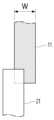
도 1은 종래기술에 따른 터치 센서의 배선 중첩부를 도시하는 일부 확대도이다.Figure 1 is an enlarged view of a portion of a wiring overlapping portion of a touch sensor according to the prior art.
도 1에 도시한 바와 같이, 제1 분할 노광으로 형성되는 제1 분할 배선(11)에 제2 분할 노광으로 제2 분할 배선(21)을 형성할 때, 공정 오차 등으로 인해 제2 분할 배선(21)이 선폭 방향으로 쉬프팅되면서 비중첩 영역이 발생하면, 비중첩 영역의 크기 감소에 따라 배선 중첩부에서의 저항이 증가하고, 그 결과 터치 센서의 성능이 떨어질 수 있다.As illustrated in Fig. 1, when forming a second split wiring (21) by a second split exposure on a first split wiring (11) formed by a first split exposure, if the second split wiring (21) shifts in the line width direction due to a process error or the like and a non-overlapping area occurs, resistance in the wiring overlapping portion increases as the size of the non-overlapping area decreases, and as a result, the performance of the touch sensor may deteriorate.
[선행기술문헌][Prior art literature]
1. 한국특허등록 제1068285호(액정표시장치 노광 마스크 패턴 및 노광 방법)1. Korean Patent Registration No. 1068285 (Liquid Crystal Display Device Exposure Mask Pattern and Exposure Method)
2. 한국특허공개 제2010-0059107호(노광 마스크)2. Korean Patent Publication No. 2010-0059107 (Exposure Mask)
본 발명은 종래기술의 이러한 문제점을 해결하기 위한 것으로,The present invention is intended to solve these problems of the prior art.
첫째, 분할 노광의 중첩 영역에서 배선이 단선되는 것을 방지 내지 최소화할 수 있고,First, it can prevent or minimize wiring disconnection in the overlapping area of split exposure,
둘째, 공정 오차로 인해 인접 배선 사이에 단락이 발생하는 것을 방지 내지 최소화할 수 있으며,Second, it can prevent or minimize short circuits between adjacent wires due to process errors.
셋째, 대면적 구현에 적용하기가 용이한, 터치 센서를 제공하고자 한다.Third, we aim to provide a touch sensor that is easy to apply to large-area implementations.
이러한 목적을 달성하기 위한 본 발명의 터치 센서는 감지부, 배선부 등을 포함할 수 있다.To achieve this purpose, the touch sensor of the present invention may include a sensing portion, a wiring portion, etc.
감지부는 배열 연결되는 다수의 감지셀을 포함할 수 있다.The sensing unit may include a plurality of sensing cells connected in an array.
배선부는 감지부에서 연결되어 감지부의 외측에 형성될 수 있다. 배선부는 분할 노광으로 형성되는 제1 분할 배선부와 제2 분할 배선부를 포함할 수 있다.The wiring portion may be formed on the outside of the sensing portion and connected to the sensing portion. The wiring portion may include a first split wiring portion and a second split wiring portion formed by split exposure.
제1 분할 배선부는 일측 단부에 배선보다 폭이 큰 연결 돌기를 갖는 제1 분할 배선을 다수 구비할 수 있다.The first split wiring section may include a plurality of first split wirings having a connecting projection having a width larger than that of the wiring at one end.
제2 분할 배선부는 일측 단부가 연결 돌기보다 작은 폭을 가지며 연결 돌기에 중첩 결합하는 제2 분할 배선을 다수 구비할 수 있다.The second split wiring section may have a plurality of second split wirings having one end having a width smaller than that of the connecting projection and overlapping and connecting to the connecting projection.
본 발명의 터치 센서에서, 연결 돌기는 사각 형상을 가질 수 있다. 사각 형상의 연결 돌기는 5~20㎛의 폭과 20~40㎛의 길이를 가질 수 있다.In the touch sensor of the present invention, the connecting protrusion may have a square shape. The connecting protrusion of the square shape may have a width of 5 to 20 μm and a length of 20 to 40 μm.
본 발명의 터치 센서에서, 연결 돌기는 원, 삼각, 또는 마름모 형상을 가질 수 있다.In the touch sensor of the present invention, the connecting protrusion may have a circular, triangular, or diamond shape.
본 발명의 터치 센서에서, 제1 분할 배선부는 일측에 배선보다 큰 폭을 갖는 장폭 배선을 갖는 제1 분할 배선을 다수 구비할 수 있다. 제2 분할 배선부는 일측에 배선보다 작은 폭을 갖고 장폭 배선에 중첩 결합하는 협폭 배선을 갖는 제2 분할 배선을 다수 구비할 수 있다.In the touch sensor of the present invention, the first split wiring section may have a plurality of first split wirings having a long-width wiring having a width greater than that of the wiring on one side. The second split wiring section may have a plurality of second split wirings having a narrow-width wiring having a width smaller than that of the wiring on one side and overlapping and connecting the long-width wiring.
본 발명의 터치 센서에서, 장폭 배선과 협폭 배선은 사각 형상을 가질 수 있다.In the touch sensor of the present invention, the long wiring and the narrow wiring may have a square shape.
본 발명에 따른 터치 센서는 일면에 윈도우층을 결합하여 윈도우 적층체의 일부를 구성할 수 있다.The touch sensor according to the present invention can form part of a window laminate by combining a window layer on one side.
본 발명에 따른 터치 센서는 일면에 디스플레이 패널을 결합하여 화상 표시 장치의 일부를 구성할 수 있다.A touch sensor according to the present invention can form part of an image display device by combining a display panel on one side.
이러한 구성을 갖는 본 발명의 터치 센서에 의하면, 제1 분할 노광에 의해 형성되는 배선의 일측 단부에 배선보다 큰 폭을 갖는 연결 돌기를 형성함으로써 제2 분할 노광으로 형성되는 배선의 일측 단부가 연결 돌기에 용이하게 중첩 연결되게 함으로써, 분할 노광의 중첩 영역에서 배선이 단선되는 것을 방지 내지 최소화할 수 있다.According to the touch sensor of the present invention having such a configuration, by forming a connecting protrusion having a width larger than the wiring at one end of the wiring formed by the first split exposure, one end of the wiring formed by the second split exposure can be easily overlapped and connected to the connecting protrusion, thereby preventing or minimizing disconnection of the wiring in the overlapping area of the split exposure.
본 발명의 터치 센서에 의하면, 제1 분할 노광과 제2 분할 노광의 공정 오차를 고려하여 연결 돌기의 폭과 길이를 최적화함으로써, 공정 오차로 인한 인접 배선 사이의 단락을 방지 내지 최소화할 수 있고, 나아가 중첩(접촉) 면적의 감소로 인한 저항 증가를 차단 내지 최소화할 수 있다.According to the touch sensor of the present invention, by optimizing the width and length of the connecting projection in consideration of the process error of the first split exposure and the second split exposure, it is possible to prevent or minimize short circuits between adjacent wires due to process error, and further, to block or minimize an increase in resistance due to a decrease in the overlapping (contact) area.
또한, 본 발명의 터치 센서에 의하면, 일정 패턴을 갖는 작은 면적의 노광 마스크를 반복 사용하여 대면적 터치 센서를 패터닝할 수 있어, 대면적 터치 센서를 형성하는데 용이하게 적용할 수 있으며, 나아가 상대적으로 가격이 비싼 대면적 마스크를 제작 또는 구입할 필요가 없으므로 제조 원가도 대폭 낮출 수 있다.In addition, according to the touch sensor of the present invention, a large-area touch sensor can be patterned by repeatedly using a small-area exposure mask having a certain pattern, so that it can be easily applied to form a large-area touch sensor, and further, since there is no need to manufacture or purchase a relatively expensive large-area mask, the manufacturing cost can also be significantly reduced.
도 1은 종래기술에 따른 터치 센서의 배선 중첩부를 도시하는 일부 확대도이다.
도 2는 본 발명에 따른 배선 중첩부를 갖는 터치 센서를 도시하는 평면도이다.
도 3a~3e는 본 발명에 따른 터치 센서에서 배선 중첩부의 형태를 도시하는 일부 확대도이다.
도 4는 발명에 따른 터치 센서에서 배선 중첩부의 중첩 마진을 설명하는 일부 확대도이다.Figure 1 is an enlarged view of a portion of a wiring overlapping portion of a touch sensor according to the prior art.
FIG. 2 is a plan view illustrating a touch sensor having a wiring overlapping portion according to the present invention.
Figures 3a to 3e are partially enlarged views showing the shape of a wiring overlapping portion in a touch sensor according to the present invention.
FIG. 4 is an enlarged view illustrating a portion of an overlapping margin of a wiring overlap portion in a touch sensor according to the invention.
이하, 첨부도면을 참조하여 본 발명을 상세히 설명한다.Hereinafter, the present invention will be described in detail with reference to the attached drawings.
도 2는 본 발명에 따른 배선 중첩부를 갖는 터치 센서를 도시하는 평면도이다.FIG. 2 is a plan view illustrating a touch sensor having a wiring overlapping portion according to the present invention.
도 2에 도시한 바와 같이, 본 발명에 따른 배선 중첩부를 갖는 터치 센서는 감지부(100), 배선부(200), 전극 패드부(300) 등을 포함할 수 있다.As illustrated in FIG. 2, a touch sensor having a wiring overlapping portion according to the present invention may include a sensing portion (100), a wiring portion (200), an electrode pad portion (300), etc.
감지부(100)는 다수의 감지셀을 포함할 수 있다. 감지셀은 X축, Y축 방향으로 배열되어 전기적으로 연결될 수 있다. 감지셀은 섬(island) 형태로 구성할 수 있고, 감지셀 사이의 전기적 연결은 감지셀과 같이 패터닝되거나 별도 공정의 브릿지를 통할 수 있다.The sensing unit (100) may include a plurality of sensing cells. The sensing cells may be arranged in the X-axis and Y-axis directions and may be electrically connected. The sensing cells may be configured in an island shape, and the electrical connection between the sensing cells may be patterned like the sensing cells or may be through a bridge of a separate process.
감지부(100)는 도전성 투명 산화물, 예를들어 인듐주석산화물(ITO), 인듐아연산화물(IZO), 알루미늄징크옥사이드(AZO), 아연산화물(ZnOx), 티타늄산화물(TiO2), 산화알루미늄(Al2O3) 등의 도전성 산화물로 구성할 수 있고, 그 밖에 인듐아연주석산화물(IZTO), 인듐 산화물(InOx), 주석 산화물(SnOx), 카드뮴 주석 산화물(CTO), 갈륨-도핑 아연 산화물(GZO), 아연주석산화물(ZTO), 인듐갈륨산화물(IGO) 등이나 이들의 2 이상 조합으로 구성할 수 있다. 감지부(100)는 도전 금속, 산화물과 금속의 적층체 등으로도 구성할 수 있는데, 도전 금속은 투명도를 높이기 위해 메쉬 타입으로 구성하는 것이 바람직할 수 있다.The sensing unit (100) can be composed of a conductive transparent oxide, for example, indium tin oxide (ITO), indium zinc oxide (IZO), aluminum zinc oxide (AZO), zinc oxide (ZnOx), titanium oxide (TiO2 ), aluminum oxide (Al2 O3 ), and the like, and in addition, indium zinc tin oxide (IZTO), indium oxide (InOx), tin oxide (SnOx), cadmium tin oxide (CTO), gallium-doped zinc oxide (GZO), zinc tin oxide (ZTO), indium gallium oxide (IGO), and the like, or a combination of two or more of these. The sensing unit (100) can also be composed of a conductive metal, a laminate of an oxide and a metal, and it may be preferable to compose the conductive metal in a mesh type to increase transparency.
배선부(200)는 감지부(100)의 외측에 형성되며, 다수의 배선을 포함할 수 있다. 배선부(200)는 일측이 감지부(100)에 연결되고 타측은 전극 패드부(300)에 연결되어, 감지부(100)의 감지 신호를 전극 패드부(300)에 전달할 수 있다.The wiring section (200) is formed on the outside of the detection section (100) and may include a plurality of wires. The wiring section (200) has one end connected to the detection section (100) and the other end connected to the electrode pad section (300), so that the detection signal of the detection section (100) can be transmitted to the electrode pad section (300).
배선부(200)는, 도 2와 같이, 감지부(100)의 외측에 전체적으로, 즉 측방 및 전후방에 배치할 수도 있고, 이와 달리 감지부(100)의 양쪽 측방과 전방(전극 패드부(300)가 형성되는 영역)에만 배치하거나, 한쪽 측방과 전방에만 배치할 수도 있다.The wiring section (200) may be arranged entirely on the outside of the detection section (100), i.e., on the sides and front and rear, as shown in FIG. 2, or alternatively, may be arranged only on both sides and the front (area where the electrode pad section (300) is formed) of the detection section (100), or may be arranged only on one side and the front.
배선부(200)는 도전 금속으로 구성할 수 있는데, 예를 들어, 은(Ag), 금(Au), 구리(Cu), 알루미늄(Al), 백금(Pt), 팔라듐(Pd), 크롬(Cr), 티타늄(Ti), 텅스텐(W), 니오븀(Nb), 탄탈륨(Ta), 바나듐(V), 철(Fe), 망간(Mn), 코발트(Co), 니켈(Ni), 아연(Zn), 또는 이들의 합금(예를 들면, 은-팔라듐-구리(APC)) 등으로 구성할 수 있다.The wiring section (200) can be composed of a conductive metal, for example, silver (Ag), gold (Au), copper (Cu), aluminum (Al), platinum (Pt), palladium (Pd), chromium (Cr), titanium (Ti), tungsten (W), niobium (Nb), tantalum (Ta), vanadium (V), iron (Fe), manganese (Mn), cobalt (Co), nickel (Ni), zinc (Zn), or an alloy thereof (for example, silver-palladium-copper (APC)).
배선부(200)는 분할 노광으로 형성할 수 있다. 분할 노광은, 도 2에 도시한 바와 같이, 제1 노광 영역(E1), 제2 노광 영역(E2) 등 다수의 노광 영역을 포함할 수 있다. 제1 노광 영역(E1)과 제2 노광 영역(E2)은 경계 영역이 중첩되어 노광되는데, 그 결과로서 제1 노광 영역(E1)과 제2 노광 영역(E2)의 경계에 중첩 노광 영역(C)이 존재할 수 있다.The wiring section (200) can be formed by split exposure. Split exposure can include multiple exposure areas, such as a first exposure area (E1) and a second exposure area (E2), as shown in Fig. 2. The first exposure area (E1) and the second exposure area (E2) are exposed with their boundary areas overlapping each other, and as a result, an overlapping exposure area (C) can exist at the boundary between the first exposure area (E1) and the second exposure area (E2).
배선부(200)는 분할 노광으로 인해 제1 분할 배선부(210), 제2 분할 배선부(220) 등을 포함할 수 있다.The wiring section (200) may include a first divided wiring section (210), a second divided wiring section (220), etc. due to divided exposure.
제1 분할 배선부(210)는 제1 노광에 의해 형성되는 다수의 제1 분할 배선(211)을 포함할 수 있다. 제1 분할 배선(211)은 배선의 일부로서, 일측 단부가 후속 분할 노광에 의해 형성되는 인접 분할 배선과 연결될 수 있다.The first split wiring portion (210) may include a plurality of first split wirings (211) formed by the first exposure. The first split wiring (211) is a part of the wiring, and one end thereof may be connected to an adjacent split wiring formed by a subsequent split exposure.
제2 분할 배선부(220)는 제2 노광에 의해 형성되는 다수의 제2 분할 배선(221)을 포함할 수 있다. 제2 분할 배선(221)은 배선의 일부로서, 전후방 단부가 앞선 분할 노광과 후속 분할 노광 의해 형성되는 전후방 인접 분할 배선과 연결될 수 있다.The second split wiring section (220) may include a plurality of second split wirings (221) formed by the second exposure. The second split wirings (221) may be part of the wiring, and their front and rear ends may be connected to front and rear adjacent split wirings formed by the previous split exposure and the subsequent split exposure.
전극 패드부(300)는 배선부(200)로부터 수신하는 감지 신호를 FPCB(미도시)로 전달하는 것으로, 다수의 전극 패드를 구비할 수 있다.The electrode pad section (300) transmits a detection signal received from the wiring section (200) to the FPCB (not shown) and may be equipped with a plurality of electrode pads.
FPCB(미도시)는 일측이 전극 패드부(300)에 접속하여 감지 신호를 직접 처리하거나 프로세서로 전달할 수 있고, 전극 패드부(300)를 통해 감지부(100)로 구동신호를 전송할 수 있다.FPCB (not shown) can be connected to an electrode pad section (300) on one side to directly process a detection signal or transmit it to a processor, and can transmit a driving signal to a detection section (100) through the electrode pad section (300).
FPCB(미도시)는 광경화성 수지를 포함하는 접착제를 이용하여 전극 패드부(300)에 접착될 수 있다. 접착제는 다수의 도전볼을 갖는 이방성 도전 필름(Anisotropic Conducting Film, ACF) 등을 이용할 수 있다.The FPCB (not shown) can be bonded to the electrode pad portion (300) using an adhesive containing a photocurable resin. The adhesive can use an anisotropic conducting film (ACF) having a plurality of conductive balls.
도 3a~3e는 본 발명에 따른 터치 센서에서 배선 중첩부의 형태를 도시하는 일부 확대도이다.Figures 3a to 3e are partially enlarged views showing the shape of a wiring overlapping portion in a touch sensor according to the present invention.
도 3a는 배선 중첩부의 제1 실시예를 도시하고 있는데, 도시한 바와 같이, 배선부(200)는 제1 노광에 의해 형성되는 제1 분할 배선부(210)의 일측 단부와 제2 노광에 의해 형성되는 제2 분할 배선부(220)의 일측 단부를 중첩시켜 형성할 수 있다.FIG. 3a illustrates a first embodiment of a wiring overlapping portion. As illustrated, a wiring portion (200) can be formed by overlapping one end of a first divided wiring portion (210) formed by a first exposure and one end of a second divided wiring portion (220) formed by a second exposure.
제1 분할 배선부(210)는 제1 분할 배선(211)을 포함할 수 있다. 제1 분할 배선(211)은 제1 배선 본체(B)와 연결 돌기(P1)를 구비할 수 있다.The first split wiring section (210) may include a first split wiring (211). The first split wiring (211) may have a first wiring body (B) and a connecting protrusion (P1).
제1 배선 본체(B)는 예를 들어 30~50㎛의 폭(W)으로 구성할 수 있고, 이격 간격은 공정 오차(5~20㎛) 등을 고려하여 20㎛를 초과하게 구성할 수 있다.The first wiring body (B) can be configured with a width (W) of, for example, 30 to 50 μm, and the spacing can be configured to exceed 20 μm in consideration of process errors (5 to 20 μm), etc.
연결 돌기(P1)는 제1 배선 본체(B)보다 큰 폭을 갖도록 구성할 수 있다. 배선을 형성할 때 발생하는 공정 오차가 최소 5㎛, 최대 20㎛까지 발생하므로, 연결 돌기(P1)의 측방 돌출 높이(H)는 5~20㎛로 구성하는 것이 바람직할 수 있다.The connecting projection (P1) can be configured to have a width greater than that of the first wiring body (B). Since a process error that occurs when forming a wiring occurs from a minimum of 5 ㎛ to a maximum of 20 ㎛, it may be desirable to configure the lateral protrusion height (H) of the connecting projection (P1) to be 5 to 20 ㎛.
연결 돌기(P1)는 사각 형상을 가질 수 있다. 이 경우, 연결 돌기(P1)의 길이는 공정 오차 등을 고려하여 최대 공정 오차보다 크게 구성하는 것이 바람직하고, 이 경우에도 측방 배선과의 단락, 길이방향 쉬프팅에 의한 저항 증가 등을 고려하여 최대 공정 오차의 2배까지 형성하는 것이 바람직할 수 있다. 이와 같이, 연결 돌기(P1)의 길이는 20~40㎛로 구성할 수 있다.The connecting projection (P1) may have a square shape. In this case, it is preferable to configure the length of the connecting projection (P1) to be greater than the maximum process error in consideration of process error, etc., and even in this case, it may be preferable to configure it to be up to twice the maximum process error in consideration of short circuits with lateral wiring, increased resistance due to longitudinal shifting, etc. In this way, the length of the connecting projection (P1) may be configured to be 20 to 40 μm.
제2 분할 배선부(220)는 제2 분할 배선(221)을 포함할 수 있다. 제2 분할 배선(221)은 배선의 일반적 크기, 즉 30~50㎛의 폭(W)을 갖도록 구성할 수 있다.The second split wiring section (220) may include a second split wiring (221). The second split wiring (221) may be configured to have a width (W) of a general wiring size, i.e., 30 to 50 μm.
제2 분할 배선(221)은 제1 분할 배선(211)의 연결 돌기(P1)보다 작은 폭을 갖고 연결 돌기(P1)에 중첩하므로, 공정 오차(측방 쉬프팅)로 인한 비중첩 리스크(인접 배선 단락, 저항 증가 등)를 해소하는데 유리할 수 있다.Since the second split wiring (221) has a smaller width than the connecting projection (P1) of the first split wiring (211) and overlaps the connecting projection (P1), it can be advantageous in eliminating the risk of non-overlapping (adjacent wiring short circuit, increased resistance, etc.) due to process error (lateral shifting).
도 3b는 배선 중첩부의 제2 실시예를 도시하고 있는데, 도시한 바와 같이, 제1 분할 배선(211)의 연결 돌기(P2)를 원 형태로 구성할 수 있다. 이 경우에도, 원형 연결 돌기(P2)는 측방 돌출 높이(H)를 5~20㎛, 길이(L)를 20~40㎛로 구성할 수 있으나, 배선이 측방으로 쉬프트되면 비중첩 영역(면적)이 사각형 연결 돌기(P1)에 비해 급속히 증가하므로, 원형 연결 돌기(P2)의 측방 돌출 높이(H)와 길이(L)는 사각형 연결 돌기(P1)의 경우보다 크게 구성하는 것이 바람직할 수 있다.FIG. 3b illustrates a second embodiment of a wiring overlapping portion. As illustrated, the connecting projection (P2) of the first split wiring (211) may be configured in a circular shape. In this case as well, the circular connecting projection (P2) may be configured to have a lateral protrusion height (H) of 5 to 20 μm and a length (L) of 20 to 40 μm. However, since the non-overlapping area (area) rapidly increases compared to that of the square connecting projection (P1) when the wiring shifts laterally, it may be desirable to configure the lateral protrusion height (H) and length (L) of the circular connecting projection (P2) to be larger than those of the square connecting projection (P1).
도 3b의 나머지 구성은 도 3a의 대응 구성과 동일하므로, 나머지 구성에 대한 상세한 설명은 도 3a의 관련 설명으로 갈음한다.Since the remaining configuration of Fig. 3b is identical to the corresponding configuration of Fig. 3a, a detailed description of the remaining configuration is replaced with the relevant description of Fig. 3a.
도 3c는 배선 중첩부의 제3 실시예를 도시하고 있는데, 도시한 바와 같이, 제1 분할 배선(211)의 연결 돌기(P3)를 삼각 형태로 구성할 수 있다. 이 경우에도, 삼각형 연결 돌기(P3)는 측방 돌출 높이(H)를 5~20㎛, 길이(L)를 20~40㎛로 구성할 수 있으나, 배선이 쉬프트되면 원형과 유사하게 비중첩 영역이 급속히 증가하므로, 삼각형 연결 돌기(P3)의 측방 돌출 높이(H)와 길이(L)는 사각형 연결 돌기(P1)의 경우보다 크게 구성하는 것이 바람직할 수 있다.Fig. 3c illustrates a third embodiment of a wiring overlapping portion. As illustrated, the connecting projection (P3) of the first split wiring (211) may be configured in a triangular shape. In this case as well, the triangular connecting projection (P3) may be configured with a lateral protrusion height (H) of 5 to 20 μm and a length (L) of 20 to 40 μm. However, since the non-overlapping area rapidly increases similarly to a circle when the wiring is shifted, it may be preferable to configure the lateral protrusion height (H) and length (L) of the triangular connecting projection (P3) to be larger than those of the square connecting projection (P1).
도 3c의 나머지 구성은 도 3a의 대응 구성과 동일하므로, 나머지 구성에 대한 상세한 설명은 도 3a의 관련 설명으로 갈음한다.Since the remaining configuration of Fig. 3c is identical to the corresponding configuration of Fig. 3a, a detailed description of the remaining configuration is replaced with the relevant description of Fig. 3a.
도 3d는 배선 중첩부의 제4 실시예를 도시하고 있는데, 도시한 바와 같이, 제1 분할 배선(211)의 연결 돌기(P4)를 마름모 형태로 구성할 수 있다. 이 경우에도, 마름모 연결 돌기(P4)는 측방 돌출 높이(H)를 5~20㎛, 길이(L)를 20~40㎛로 구성할 수 있으나, 배선이 쉬프트되면 원형, 삼각형과 유사하게 비중첩 영역이 증가하므로, 마름모 연결 돌기(P4)의 측방 돌출 높이(H)와 길이(L)도 사각형 연결 돌기(P1)의 경우보다 크게 구성하는 것이 바람직할 수 있다.FIG. 3d illustrates a fourth embodiment of a wiring overlapping portion. As illustrated, the connecting projection (P4) of the first split wiring (211) may be configured in a diamond shape. In this case, the diamond-shaped connecting projection (P4) may be configured to have a lateral protrusion height (H) of 5 to 20 μm and a length (L) of 20 to 40 μm. However, since the non-overlapping area increases similarly to a circle or triangle when the wiring is shifted, it may be desirable to configure the lateral protrusion height (H) and length (L) of the diamond-shaped connecting projection (P4) to be larger than those of the square connecting projection (P1).
도 3d의 나머지 구성은 도 3a의 대응 구성과 동일하므로, 나머지 구성에 대한 상세한 설명은 도 3a의 관련 설명으로 갈음한다.Since the remaining configuration of Fig. 3d is identical to the corresponding configuration of Fig. 3a, a detailed description of the remaining configuration is replaced with the relevant description of Fig. 3a.
도 3e는 배선 중첩부의 제5 실시예를 도시하고 있는데, 도시한 바와 같이, 제1 분할 배선(211)은 일측에 배선보다 큰 폭을 갖는 제1 장폭 배선(WW1)을 구비할 수 있다. 제1 장폭 배선(WW1)은 사각 형상으로 구성할 수 있고, 제1 장폭 배선(WW1)의 측방 돌출 높이(H)는 공정 오차 등을 고려하여 5~20㎛로 구성하고, 길이(L)는 40㎛ 이상으로 구성할 수 있다. 제1 분할 배선(211)에서 제1 장폭 배선(WW1)을 제외한 나머지 배선 부분은 일반적인 배선과 동일한 폭으로 구성하거나 일반적인 배선보다 작은 폭을 갖는 제1 협폭 배선(NW1)으로 구성할 수도 있다.FIG. 3e illustrates a fifth embodiment of a wiring overlapping portion. As illustrated, the first split wiring (211) may have a first wide wiring (WW1) having a width larger than that of the wiring on one side. The first wide wiring (WW1) may be configured in a square shape, and the lateral protrusion height (H) of the first wide wiring (WW1) may be configured to be 5 to 20 μm in consideration of process errors, etc., and the length (L) may be configured to be 40 μm or more. In the first split wiring (211), the remaining wiring portion excluding the first wide wiring (WW1) may be configured to have the same width as a general wiring, or may be configured as a first narrow wiring (NW1) having a width smaller than that of a general wiring.
도 3e에서, 제2 분할 배선(221)은 제1 분할 배선(211)의 제1 장폭 배선(WW1)에 중첩 결합하는 제2 협폭 배선(NW2)을 구비할 수 있다. 제2 협폭 배선(NW2)은 사각 형상으로 구성할 수 있다. 제2 협폭 배선(NW2)은 일반적인 배선과 동일한 폭으로 구성하거나 일반적 배선보다 작은 폭으로 구성할 수 있다. 제2 분할 배선(221)에서 제2 협폭 배선(NW2)을 제외한 나머지 배선 부분은 일반적인 배선과 동일한 폭으로 구성하거나 일반적인 배선보다 큰 폭을 갖는 제2 광폭 배선(WW2)으로 구성할 수도 있다.In FIG. 3e, the second split wiring (221) may have a second narrow wiring (NW2) that overlaps and is connected to the first wide wiring (WW1) of the first split wiring (211). The second narrow wiring (NW2) may be configured in a square shape. The second narrow wiring (NW2) may be configured with the same width as a general wiring or may be configured with a width smaller than a general wiring. The remaining wiring portion of the second split wiring (221) excluding the second narrow wiring (NW2) may be configured with the same width as a general wiring or may be configured with a second wide wiring (WW2) that has a width larger than a general wiring.
도 3e의 나머지 구성은 도 3a의 대응 구성과 동일하므로, 나머지 구성에 대한 상세한 설명은 도 3a의 관련 설명으로 갈음한다.Since the remaining configuration of Fig. 3e is identical to the corresponding configuration of Fig. 3a, a detailed description of the remaining configuration is replaced with the relevant description of Fig. 3a.
도 4는 발명에 따른 터치 센서에서 배선 중첩부의 중첩 마진을 설명하는 일부 확대도이다.FIG. 4 is an enlarged view illustrating a portion of an overlapping margin of a wiring overlap portion in a touch sensor according to the invention.
도 4에 도시한 바와 같이, 제1 분할 노광으로 형성되는 제1 분할 배선(211)에서 연결 돌기(P1)의 폭을 일반적인 배선보다 큰 폭으로 형성하면, 제2 분할 노광으로 형성되는 제2 분할 배선(221)의 일측 단부가 중첩될 때 측방 쉬프트 마진을 높일 수 있다. 여기서, 배선부를 형성할 때 발생하는 공정 오차의 최대값이 20㎛임을 고려하여 연결 돌기(P1)의 측방 돌출 높이(H)를 20㎛로 형성하면, 공정 오차(측방 쉬프트)로 인해 제2 분할 배선(221)이 쉬프트되더라도 제1 분할 배선(211)과 제2 분할 배선(221) 사이에 비중첩 영역이 발생하는 것을 원천적으로 차단하거나 최소화할 수 있다.As illustrated in FIG. 4, if the width of the connecting projection (P1) in the first split wiring (211) formed by the first split exposure is formed to be larger than that of a general wiring, the lateral shift margin can be increased when one end of the second split wiring (221) formed by the second split exposure overlaps. Here, considering that the maximum value of the process error occurring when forming the wiring portion is 20 ㎛, if the lateral protrusion height (H) of the connecting projection (P1) is formed to be 20 ㎛, even if the second split wiring (221) shifts due to the process error (lateral shift), the occurrence of a non-overlapping area between the first split wiring (211) and the second split wiring (221) can be fundamentally blocked or minimized.
한편, 제1 분할 노광으로 형성되는 제1 분할 배선(211)에서 연결 돌기(P1)의 길이를 공정 오차의 최대값인 20㎛보다 크게 형성하면, 제2 분할 노광으로 형성되는 제2 분할 배선(221)의 일측 단부와 연결 돌기(P1)의 중첩 길이(T)를 최소 20㎛를 확보할 수 있어, 제2 분할 배선(221)이 공정 오차의 최대값인 20㎛까지 측방으로 쉬프트되더라도 제2 분할 배선(221)은 제1 분할 배선(211)과 최대 20 X 20㎛의 면적으로 중첩될 수 있고, 그 결과 제1 분할 배선(211)과 제2 분할 배선(221)의 비중첩으로 발생하는 저항 증가를 차단 내지 최소화할 수 있다. 나아가, 제2 분할 배선(221)이 공정 오차의 최대값인 20㎛까지 길이방향으로 쉬프트되는 경우까지 고려하면, 연결 돌기(P1)의 길이(L)는 40㎛까지 구성하는 것이 바람직할 수 있다.Meanwhile, if the length of the connecting projection (P1) in the first split wiring (211) formed by the first split exposure is formed to be greater than 20 ㎛, which is the maximum value of the process error, the overlapping length (T) of one end of the second split wiring (221) formed by the second split exposure and the connecting projection (P1) can be secured to at least 20 ㎛, so that even if the second split wiring (221) is shifted laterally by 20 ㎛, which is the maximum value of the process error, the second split wiring (221) can overlap the first split wiring (211) by an area of at most 20 X 20 ㎛, and as a result, the increase in resistance caused by the non-overlapping of the first split wiring (211) and the second split wiring (221) can be blocked or minimized. Furthermore, considering the case where the second split wiring (221) shifts in the longitudinal direction by up to 20 ㎛, which is the maximum value of the process error, it may be desirable to configure the length (L) of the connecting protrusion (P1) to up to 40 ㎛.
본 발명에 따른 배선 중첩부를 갖는 터치 센서는 일면에 윈도우층을 결합하여 윈도우 적층체의 일부를 구성할 수 있다. 여기서, 윈도우층은 윈도우층은 투명 필름, 편광층, 데코층 등을 포함할 수 있다.A touch sensor having a wiring overlap according to the present invention can form a part of a window laminate by combining a window layer on one side. Here, the window layer can include a transparent film, a polarizing layer, a decorative layer, etc.
본 발명에 따른 배선 중첩부를 갖는 터치 센서는 일면에 디스플레이 패널을 결합하여 화상 표시 장치의 일부를 구성할 수 있다. 여기서, 디스플레이 패널은 액정표시 패널, 플라즈마 패널, 전계발광 패널, 유기발광다이오드 패널 등을 포함할 수 있다.A touch sensor having a wiring overlapping portion according to the present invention can form a part of an image display device by combining a display panel on one side. Here, the display panel can include a liquid crystal display panel, a plasma panel, an electroluminescent panel, an organic light-emitting diode panel, etc.
이상 본 발명을 여러 실시예로 설명하였으나, 이는 본 발명을 예증하기 위한 것이다. 통상의 기술자라면 이러한 실시예를 다른 형태로 변형하거나 수정할 수 있을 것이다. 그러나, 본 발명의 권리범위는 아래의 특허청구범위에 의해 정해지므로, 그러한 변형이나 수정이 본 발명의 권리범위에 포함되는 것으로 해석될 수 있다.Although the present invention has been described in several embodiments, this is for the purpose of illustrating the present invention. Those skilled in the art may modify or alter these embodiments in other forms. However, since the scope of the present invention is determined by the following claims, such modifications or alterations may be interpreted as being included in the scope of the present invention.
100 : 감지부200 : 배선부
210 : 제1 분할 배선부211 : 제1 분할 배선
220 : 제2 분할 배선부221 : 제2 분할 배선
300 : 전극 패드부E1 : 제1 노광 영역
E2 : 제2 노광 영역C : 중첩 노광 영역
B : 배선 본체P1~P4 ; 연결 돌기
NW1 : 제1 협폭 배선NW2 : 제2 협폭 배선
WW1 : 제1 광폭 배선WW2 : 제2 광폭 배선
W : 배선 폭H : 연결 돌기의 측방 돌출 높이
L : 연결 돌기의 길이T : 중첩 길이100: Detection section 200: Wiring section
210: 1st split wiring section 211: 1st split wiring section
220: Second split wiring section 221: Second split wiring section
300: Electrode pad area E1: First exposure area
E2: Second exposure area C: Overlapping exposure area
B: Wiring body P1~P4; Connecting projection
NW1: 1st narrow-width wiring NW2: 2nd narrow-width wiring
WW1: First Wide Width Warfare WW2: Second Wide Width Warfare
W: Width of the wiring H: Lateral protrusion height of the connecting projection
L: Length of connecting projection T: Overlapping length
Claims (8)
Translated fromKorean상기 감지부에서 연결되어 상기 감지부의 외측에 형성되는 배선부를 포함하고,
상기 배선부는
제1 분할 배선과 상기 제1 분할 배선에 분할 노광으로 중첩 형성되는 제2 분할 배선을 포함하고,
상기 제1 분할 배선은 제1 배선 본체와 상기 제1 배선 본체의 일측 단부에 연결되고 상기 제1 배선 본체보다 폭이 넓은 제1 연결 돌기를 포함하고,
상기 제2 분할 배선은 일측 단부가 상기 제1 연결 돌기보다 폭이 좁으면서 상기 제1 연결 돌기에 중첩 결합하며,
상기 제1 분할 배선은 인접하는 다른 제1 분할 배선과 20㎛ 를 초과하여 이격되고,
상기 제1 연결 돌기는, 장변과 단변을 갖는 사각 형상을 가지며, 상기 제1 배선 본체의 측방에서 폭방향 양측으로 각각 5~20㎛ 로 돌출하고, 그리고 상기 제1 배선 본체의 일측 단부에서 길이방향을 따라 외측으로 20~40㎛ 로 연장하는, 배선 중첩부를 갖는 터치 센서.A sensing unit in which a plurality of sensing cells are connected in an array; and
Includes a wiring section that is connected to the above detection section and formed on the outside of the above detection section,
The above wiring section
It includes a first split wiring and a second split wiring formed by overlapping the first split wiring with split exposure,
The above first split wiring includes a first wiring body and a first connecting protrusion connected to one end of the first wiring body and having a wider width than the first wiring body,
The second split wiring has one end narrower than the first connecting projection and overlaps and connects to the first connecting projection,
The above first division wiring is spaced apart from the adjacent other first division wiring by more than 20㎛,
A touch sensor having a wiring overlapping portion in which the above first connecting protrusion has a square shape having a long side and a short side, protrudes 5 to 20 μm on both sides in the width direction from the side of the first wiring body, and extends outwardly 20 to 40 μm along the length direction from one end of the first wiring body.
상기 감지부에서 연결되어 상기 감지부의 외측에 형성되는 배선부를 포함하고,
상기 배선부는
제1 분할 배선과 상기 제1 분할 배선에 분할 노광으로 중첩 형성되는 제2 분할 배선을 포함하고,
상기 제1 분할 배선은 제1 협폭 배선과 상기 제1 협폭 배선의 일측 단부에 연결되고 상기 제1 협폭 배선보다 폭이 넓은 제1 광폭 배선을 포함하고,
상기 제2 분할 배선은 제2 광폭 배선과 상기 제2 광폭 배선의 일측 단부에 연결되고 상기 제2 광폭 배선 및 상기 제1 광폭 배선보다 폭이 좁은 제2 협폭 배선을 포함하여 상기 제2 협폭 배선이 상기 제1 광폭 배선에 중첩 결합하며,
상기 제1 분할 배선은 인접하는 다른 제1 분할 배선과 20㎛ 를 초과하여 이격되고,
상기 제1 광폭 배선은, 장변과 단변을 갖는 사각 형상을 가지며, 상기 제1 협폭 배선의 측방에서 폭방향 양측으로 각각 5~20㎛ 로 돌출하고, 그리고 상기 제1 협폭 배선의 일측 단부에서 길이방향을 따라 외측으로 20~40㎛ 로 연장하는, 배선 중첩부를 갖는 터치 센서.A detection unit in which a plurality of detection cells are connected in an array; and
Includes a wiring section that is connected to the above detection section and formed on the outside of the above detection section,
The above wiring section
It includes a first split wiring and a second split wiring formed by overlapping the first split wiring with split exposure,
The above first split wiring includes a first narrow wiring and a first wide wiring connected to one end of the first narrow wiring and having a width wider than the first narrow wiring,
The second split wiring is connected to the second wide wiring and one end of the second wide wiring, and includes a second narrow wiring having a width narrower than the second wide wiring and the first wide wiring, such that the second narrow wiring is overlapped and connected to the first wide wiring,
The above first division wiring is spaced apart from the adjacent other first division wiring by more than 20㎛,
A touch sensor having a wire overlapping portion in which the first wide wiring has a rectangular shape having a long side and a short side, and protrudes 5 to 20 μm on both sides in the width direction from the side of the first narrow wiring, and extends outward 20 to 40 μm along the length direction from one end of the first narrow wiring.
상기 터치 센서의 일면에 결합하는 윈도우층을 포함하는, 윈도우 적층체.A touch sensor having a wiring overlap according to claim 1 or claim 5; and
A window laminate comprising a window layer coupled to one surface of the touch sensor.
상기 터치 센서의 일면에 결합하는 디스플레이 패널을 포함하는, 화상 표시 장치.A touch sensor having a wiring overlap according to claim 1 or claim 5; and
An image display device comprising a display panel coupled to one side of the touch sensor.
Priority Applications (4)
| Application Number | Priority Date | Filing Date | Title |
|---|---|---|---|
| KR1020200100093AKR102804441B1 (en) | 2020-08-10 | 2020-08-10 | Touch Sensor with Overlapped Wiring |
| CN202180056169.7ACN116113916A (en) | 2020-08-10 | 2021-08-04 | Touch sensor with routing overlap |
| US18/040,926US11941221B2 (en) | 2020-08-10 | 2021-08-04 | Touch sensor having wiring overlapping part |
| PCT/KR2021/010243WO2022035122A1 (en) | 2020-08-10 | 2021-08-04 | Touch sensor having wiring overlapping part |
Applications Claiming Priority (1)
| Application Number | Priority Date | Filing Date | Title |
|---|---|---|---|
| KR1020200100093AKR102804441B1 (en) | 2020-08-10 | 2020-08-10 | Touch Sensor with Overlapped Wiring |
Publications (2)
| Publication Number | Publication Date |
|---|---|
| KR20220019543A KR20220019543A (en) | 2022-02-17 |
| KR102804441B1true KR102804441B1 (en) | 2025-05-07 |
Family
ID=80247114
Family Applications (1)
| Application Number | Title | Priority Date | Filing Date |
|---|---|---|---|
| KR1020200100093AActiveKR102804441B1 (en) | 2020-08-10 | 2020-08-10 | Touch Sensor with Overlapped Wiring |
Country Status (4)
| Country | Link |
|---|---|
| US (1) | US11941221B2 (en) |
| KR (1) | KR102804441B1 (en) |
| CN (1) | CN116113916A (en) |
| WO (1) | WO2022035122A1 (en) |
Family Cites Families (10)
| Publication number | Priority date | Publication date | Assignee | Title |
|---|---|---|---|---|
| US5364718A (en)* | 1988-09-06 | 1994-11-15 | Fujitsu Limited | Method of exposing patttern of semiconductor devices and stencil mask for carrying out same |
| JPH05136020A (en) | 1991-11-11 | 1993-06-01 | Fujitsu Ltd | Exposure method of semiconductor device |
| KR20000027743A (en)* | 1998-10-29 | 2000-05-15 | 김영환 | Method for forming shot pattern |
| KR101068285B1 (en) | 2004-09-13 | 2011-09-28 | 엘지디스플레이 주식회사 | LCD display exposure mask pattern and exposure method |
| JP2007103723A (en) | 2005-10-05 | 2007-04-19 | Renesas Technology Corp | Semiconductor device, and method of manufacturing same |
| JP2010098095A (en) | 2008-10-16 | 2010-04-30 | Sony Corp | Semiconductor device, and method of manufacturing the same |
| KR20100059107A (en) | 2008-11-25 | 2010-06-04 | 엘지디스플레이 주식회사 | Exposure mask |
| KR20160079281A (en)* | 2014-12-26 | 2016-07-06 | 엘지이노텍 주식회사 | Touch window |
| CN112860130A (en)* | 2019-11-26 | 2021-05-28 | 英属维尔京群岛商天材创新材料科技股份有限公司 | Touch panel and manufacturing method thereof |
| US11215923B1 (en)* | 2020-08-03 | 2022-01-04 | Young Fast Optoelectronics Co., Ltd. | Method for manufacturing large-scale touch sensing pattern |
- 2020
- 2020-08-10KRKR1020200100093Apatent/KR102804441B1/enactiveActive
- 2021
- 2021-08-04USUS18/040,926patent/US11941221B2/enactiveActive
- 2021-08-04WOPCT/KR2021/010243patent/WO2022035122A1/ennot_activeCeased
- 2021-08-04CNCN202180056169.7Apatent/CN116113916A/enactivePending
Also Published As
| Publication number | Publication date |
|---|---|
| US20230297202A1 (en) | 2023-09-21 |
| KR20220019543A (en) | 2022-02-17 |
| WO2022035122A1 (en) | 2022-02-17 |
| CN116113916A (en) | 2023-05-12 |
| US11941221B2 (en) | 2024-03-26 |
Similar Documents
| Publication | Publication Date | Title |
|---|---|---|
| TWI525487B (en) | Touch screen panel and display device having the same | |
| US9354756B2 (en) | Touch screen panel and display device having the same | |
| US9791982B2 (en) | Touch screen panel having compensation patterns | |
| US20120105339A1 (en) | Flat panel display with built-in touch panel | |
| KR102036293B1 (en) | Electrode connection structure and touch sensor | |
| US11775096B2 (en) | Electrode structure combined with antenna and display device including the same | |
| CN114077347B (en) | Antenna insertion type electrode structure and image display device | |
| CN113268154A (en) | Antenna insertion type electrode structure and image display device | |
| KR102015864B1 (en) | Touch sensor and display device including the same | |
| KR102162657B1 (en) | Touch sensor and image display device including the same | |
| CN214151675U (en) | Antenna structure and image display device | |
| CN212933498U (en) | Antenna structure and image display device | |
| KR20160133603A (en) | Touch screen panel | |
| KR102804441B1 (en) | Touch Sensor with Overlapped Wiring | |
| CN213399537U (en) | Antenna structure and image display device | |
| CN213816404U (en) | Antenna module and display device including the same | |
| JP7526839B2 (en) | Touch Sensor | |
| KR102520036B1 (en) | Stepper Mask for Fabricating Touch Sensor | |
| KR20190132259A (en) | Pressure sensor and image display device including the same | |
| KR20170079956A (en) | Liquid crystal display device | |
| KR102526899B1 (en) | Touch sensor and image display device including the same | |
| KR102288728B1 (en) | Touch screen panel and display device comprising the same | |
| KR20190132262A (en) | Pressure sensor and image display device including the same | |
| KR20240131617A (en) | Digitizer, manufacturing method thereof, and image display device including the same | |
| TW202309726A (en) | Touch sensor |
Legal Events
| Date | Code | Title | Description |
|---|---|---|---|
| PA0109 | Patent application | Patent event code:PA01091R01D Comment text:Patent Application Patent event date:20200810 | |
| PG1501 | Laying open of application | ||
| A201 | Request for examination | ||
| PA0201 | Request for examination | Patent event code:PA02012R01D Patent event date:20230314 Comment text:Request for Examination of Application Patent event code:PA02011R01I Patent event date:20200810 Comment text:Patent Application | |
| E902 | Notification of reason for refusal | ||
| PE0902 | Notice of grounds for rejection | Comment text:Notification of reason for refusal Patent event date:20240822 Patent event code:PE09021S01D | |
| E701 | Decision to grant or registration of patent right | ||
| PE0701 | Decision of registration | Patent event code:PE07011S01D Comment text:Decision to Grant Registration Patent event date:20250428 | |
| GRNT | Written decision to grant | ||
| PR0701 | Registration of establishment | Comment text:Registration of Establishment Patent event date:20250430 Patent event code:PR07011E01D | |
| PR1002 | Payment of registration fee | Payment date:20250430 End annual number:3 Start annual number:1 | |
| PG1601 | Publication of registration |