KR102801448B1 - Memory device having vertical structure - Google Patents
Memory device having vertical structureDownload PDFInfo
- Publication number
- KR102801448B1 KR102801448B1KR1020200137044AKR20200137044AKR102801448B1KR 102801448 B1KR102801448 B1KR 102801448B1KR 1020200137044 AKR1020200137044 AKR 1020200137044AKR 20200137044 AKR20200137044 AKR 20200137044AKR 102801448 B1KR102801448 B1KR 102801448B1
- Authority
- KR
- South Korea
- Prior art keywords
- page buffer
- group
- circuit
- wafer
- voltage
- Prior art date
- Legal status (The legal status is an assumption and is not a legal conclusion. Google has not performed a legal analysis and makes no representation as to the accuracy of the status listed.)
- Active
Links
Images


Classifications
- H—ELECTRICITY
- H01—ELECTRIC ELEMENTS
- H01L—SEMICONDUCTOR DEVICES NOT COVERED BY CLASS H10
- H01L24/00—Arrangements for connecting or disconnecting semiconductor or solid-state bodies; Methods or apparatus related thereto
- H01L24/01—Means for bonding being attached to, or being formed on, the surface to be connected, e.g. chip-to-package, die-attach, "first-level" interconnects; Manufacturing methods related thereto
- H01L24/02—Bonding areas ; Manufacturing methods related thereto
- H01L24/07—Structure, shape, material or disposition of the bonding areas after the connecting process
- H01L24/08—Structure, shape, material or disposition of the bonding areas after the connecting process of an individual bonding area
- G—PHYSICS
- G11—INFORMATION STORAGE
- G11C—STATIC STORES
- G11C5/00—Details of stores covered by group G11C11/00
- G11C5/06—Arrangements for interconnecting storage elements electrically, e.g. by wiring
- G11C5/063—Voltage and signal distribution in integrated semi-conductor memory access lines, e.g. word-line, bit-line, cross-over resistance, propagation delay
- G—PHYSICS
- G11—INFORMATION STORAGE
- G11C—STATIC STORES
- G11C16/00—Erasable programmable read-only memories
- G11C16/02—Erasable programmable read-only memories electrically programmable
- G11C16/04—Erasable programmable read-only memories electrically programmable using variable threshold transistors, e.g. FAMOS
- G11C16/0483—Erasable programmable read-only memories electrically programmable using variable threshold transistors, e.g. FAMOS comprising cells having several storage transistors connected in series
- G—PHYSICS
- G11—INFORMATION STORAGE
- G11C—STATIC STORES
- G11C16/00—Erasable programmable read-only memories
- G11C16/02—Erasable programmable read-only memories electrically programmable
- G11C16/06—Auxiliary circuits, e.g. for writing into memory
- G—PHYSICS
- G11—INFORMATION STORAGE
- G11C—STATIC STORES
- G11C16/00—Erasable programmable read-only memories
- G11C16/02—Erasable programmable read-only memories electrically programmable
- G11C16/06—Auxiliary circuits, e.g. for writing into memory
- G11C16/08—Address circuits; Decoders; Word-line control circuits
- G—PHYSICS
- G11—INFORMATION STORAGE
- G11C—STATIC STORES
- G11C16/00—Erasable programmable read-only memories
- G11C16/02—Erasable programmable read-only memories electrically programmable
- G11C16/06—Auxiliary circuits, e.g. for writing into memory
- G11C16/10—Programming or data input circuits
- G—PHYSICS
- G11—INFORMATION STORAGE
- G11C—STATIC STORES
- G11C16/00—Erasable programmable read-only memories
- G11C16/02—Erasable programmable read-only memories electrically programmable
- G11C16/06—Auxiliary circuits, e.g. for writing into memory
- G11C16/30—Power supply circuits
- G—PHYSICS
- G11—INFORMATION STORAGE
- G11C—STATIC STORES
- G11C5/00—Details of stores covered by group G11C11/00
- G11C5/02—Disposition of storage elements, e.g. in the form of a matrix array
- G11C5/025—Geometric lay-out considerations of storage- and peripheral-blocks in a semiconductor storage device
- G—PHYSICS
- G11—INFORMATION STORAGE
- G11C—STATIC STORES
- G11C7/00—Arrangements for writing information into, or reading information out from, a digital store
- G11C7/10—Input/output [I/O] data interface arrangements, e.g. I/O data control circuits, I/O data buffers
- H—ELECTRICITY
- H01—ELECTRIC ELEMENTS
- H01L—SEMICONDUCTOR DEVICES NOT COVERED BY CLASS H10
- H01L25/00—Assemblies consisting of a plurality of semiconductor or other solid state devices
- H01L25/03—Assemblies consisting of a plurality of semiconductor or other solid state devices all the devices being of a type provided for in a single subclass of subclasses H10B, H10D, H10F, H10H, H10K or H10N, e.g. assemblies of rectifier diodes
- H01L25/04—Assemblies consisting of a plurality of semiconductor or other solid state devices all the devices being of a type provided for in a single subclass of subclasses H10B, H10D, H10F, H10H, H10K or H10N, e.g. assemblies of rectifier diodes the devices not having separate containers
- H01L25/065—Assemblies consisting of a plurality of semiconductor or other solid state devices all the devices being of a type provided for in a single subclass of subclasses H10B, H10D, H10F, H10H, H10K or H10N, e.g. assemblies of rectifier diodes the devices not having separate containers the devices being of a type provided for in group H10D89/00
- H01L25/0657—Stacked arrangements of devices
- H—ELECTRICITY
- H01—ELECTRIC ELEMENTS
- H01L—SEMICONDUCTOR DEVICES NOT COVERED BY CLASS H10
- H01L25/00—Assemblies consisting of a plurality of semiconductor or other solid state devices
- H01L25/18—Assemblies consisting of a plurality of semiconductor or other solid state devices the devices being of the types provided for in two or more different main groups of the same subclass of H10B, H10D, H10F, H10H, H10K or H10N
- H—ELECTRICITY
- H01—ELECTRIC ELEMENTS
- H01L—SEMICONDUCTOR DEVICES NOT COVERED BY CLASS H10
- H01L25/00—Assemblies consisting of a plurality of semiconductor or other solid state devices
- H01L25/50—Multistep manufacturing processes of assemblies consisting of devices, the devices being individual devices of subclass H10D or integrated devices of class H10
- H—ELECTRICITY
- H10—SEMICONDUCTOR DEVICES; ELECTRIC SOLID-STATE DEVICES NOT OTHERWISE PROVIDED FOR
- H10B—ELECTRONIC MEMORY DEVICES
- H10B43/00—EEPROM devices comprising charge-trapping gate insulators
- H10B43/20—EEPROM devices comprising charge-trapping gate insulators characterised by three-dimensional arrangements, e.g. with cells on different height levels
- H10B43/23—EEPROM devices comprising charge-trapping gate insulators characterised by three-dimensional arrangements, e.g. with cells on different height levels with source and drain on different levels, e.g. with sloping channels
- H10B43/27—EEPROM devices comprising charge-trapping gate insulators characterised by three-dimensional arrangements, e.g. with cells on different height levels with source and drain on different levels, e.g. with sloping channels the channels comprising vertical portions, e.g. U-shaped channels
- H—ELECTRICITY
- H10—SEMICONDUCTOR DEVICES; ELECTRIC SOLID-STATE DEVICES NOT OTHERWISE PROVIDED FOR
- H10B—ELECTRONIC MEMORY DEVICES
- H10B43/00—EEPROM devices comprising charge-trapping gate insulators
- H10B43/30—EEPROM devices comprising charge-trapping gate insulators characterised by the memory core region
- H10B43/35—EEPROM devices comprising charge-trapping gate insulators characterised by the memory core region with cell select transistors, e.g. NAND
- H—ELECTRICITY
- H10—SEMICONDUCTOR DEVICES; ELECTRIC SOLID-STATE DEVICES NOT OTHERWISE PROVIDED FOR
- H10B—ELECTRONIC MEMORY DEVICES
- H10B43/00—EEPROM devices comprising charge-trapping gate insulators
- H10B43/40—EEPROM devices comprising charge-trapping gate insulators characterised by the peripheral circuit region
- H—ELECTRICITY
- H10—SEMICONDUCTOR DEVICES; ELECTRIC SOLID-STATE DEVICES NOT OTHERWISE PROVIDED FOR
- H10B—ELECTRONIC MEMORY DEVICES
- H10B43/00—EEPROM devices comprising charge-trapping gate insulators
- H10B43/50—EEPROM devices comprising charge-trapping gate insulators characterised by the boundary region between the core and peripheral circuit regions
- G—PHYSICS
- G11—INFORMATION STORAGE
- G11C—STATIC STORES
- G11C2211/00—Indexing scheme relating to digital stores characterized by the use of particular electric or magnetic storage elements; Storage elements therefor
- G11C2211/56—Indexing scheme relating to G11C11/56 and sub-groups for features not covered by these groups
- G11C2211/564—Miscellaneous aspects
- G11C2211/5642—Multilevel memory with buffers, latches, registers at input or output
- H—ELECTRICITY
- H01—ELECTRIC ELEMENTS
- H01L—SEMICONDUCTOR DEVICES NOT COVERED BY CLASS H10
- H01L2224/00—Indexing scheme for arrangements for connecting or disconnecting semiconductor or solid-state bodies and methods related thereto as covered by H01L24/00
- H01L2224/01—Means for bonding being attached to, or being formed on, the surface to be connected, e.g. chip-to-package, die-attach, "first-level" interconnects; Manufacturing methods related thereto
- H01L2224/02—Bonding areas; Manufacturing methods related thereto
- H01L2224/04—Structure, shape, material or disposition of the bonding areas prior to the connecting process
- H01L2224/05—Structure, shape, material or disposition of the bonding areas prior to the connecting process of an individual bonding area
- H01L2224/0554—External layer
- H01L2224/0555—Shape
- H01L2224/05556—Shape in side view
- H—ELECTRICITY
- H01—ELECTRIC ELEMENTS
- H01L—SEMICONDUCTOR DEVICES NOT COVERED BY CLASS H10
- H01L2224/00—Indexing scheme for arrangements for connecting or disconnecting semiconductor or solid-state bodies and methods related thereto as covered by H01L24/00
- H01L2224/01—Means for bonding being attached to, or being formed on, the surface to be connected, e.g. chip-to-package, die-attach, "first-level" interconnects; Manufacturing methods related thereto
- H01L2224/02—Bonding areas; Manufacturing methods related thereto
- H01L2224/07—Structure, shape, material or disposition of the bonding areas after the connecting process
- H01L2224/08—Structure, shape, material or disposition of the bonding areas after the connecting process of an individual bonding area
- H01L2224/0805—Shape
- H01L2224/08057—Shape in side view
- H01L2224/08058—Shape in side view being non uniform along the bonding area
- H—ELECTRICITY
- H01—ELECTRIC ELEMENTS
- H01L—SEMICONDUCTOR DEVICES NOT COVERED BY CLASS H10
- H01L2224/00—Indexing scheme for arrangements for connecting or disconnecting semiconductor or solid-state bodies and methods related thereto as covered by H01L24/00
- H01L2224/01—Means for bonding being attached to, or being formed on, the surface to be connected, e.g. chip-to-package, die-attach, "first-level" interconnects; Manufacturing methods related thereto
- H01L2224/02—Bonding areas; Manufacturing methods related thereto
- H01L2224/07—Structure, shape, material or disposition of the bonding areas after the connecting process
- H01L2224/08—Structure, shape, material or disposition of the bonding areas after the connecting process of an individual bonding area
- H01L2224/081—Disposition
- H01L2224/0812—Disposition the bonding area connecting directly to another bonding area, i.e. connectorless bonding, e.g. bumpless bonding
- H01L2224/08135—Disposition the bonding area connecting directly to another bonding area, i.e. connectorless bonding, e.g. bumpless bonding the bonding area connecting between different semiconductor or solid-state bodies, i.e. chip-to-chip
- H01L2224/08145—Disposition the bonding area connecting directly to another bonding area, i.e. connectorless bonding, e.g. bumpless bonding the bonding area connecting between different semiconductor or solid-state bodies, i.e. chip-to-chip the bodies being stacked
- H—ELECTRICITY
- H01—ELECTRIC ELEMENTS
- H01L—SEMICONDUCTOR DEVICES NOT COVERED BY CLASS H10
- H01L2225/00—Details relating to assemblies covered by the group H01L25/00 but not provided for in its subgroups
- H01L2225/03—All the devices being of a type provided for in the same main group of the same subclass of class H10, e.g. assemblies of rectifier diodes
- H01L2225/04—All the devices being of a type provided for in the same main group of the same subclass of class H10, e.g. assemblies of rectifier diodes the devices not having separate containers
- H01L2225/065—All the devices being of a type provided for in the same main group of the same subclass of class H10
- H01L2225/06503—Stacked arrangements of devices
- H01L2225/06524—Electrical connections formed on device or on substrate, e.g. a deposited or grown layer
- H—ELECTRICITY
- H01—ELECTRIC ELEMENTS
- H01L—SEMICONDUCTOR DEVICES NOT COVERED BY CLASS H10
- H01L2225/00—Details relating to assemblies covered by the group H01L25/00 but not provided for in its subgroups
- H01L2225/03—All the devices being of a type provided for in the same main group of the same subclass of class H10, e.g. assemblies of rectifier diodes
- H01L2225/04—All the devices being of a type provided for in the same main group of the same subclass of class H10, e.g. assemblies of rectifier diodes the devices not having separate containers
- H01L2225/065—All the devices being of a type provided for in the same main group of the same subclass of class H10
- H01L2225/06503—Stacked arrangements of devices
- H01L2225/06541—Conductive via connections through the device, e.g. vertical interconnects, through silicon via [TSV]
- H—ELECTRICITY
- H01—ELECTRIC ELEMENTS
- H01L—SEMICONDUCTOR DEVICES NOT COVERED BY CLASS H10
- H01L2924/00—Indexing scheme for arrangements or methods for connecting or disconnecting semiconductor or solid-state bodies as covered by H01L24/00
- H01L2924/10—Details of semiconductor or other solid state devices to be connected
- H01L2924/11—Device type
- H01L2924/14—Integrated circuits
- H01L2924/143—Digital devices
- H01L2924/1431—Logic devices
- H—ELECTRICITY
- H01—ELECTRIC ELEMENTS
- H01L—SEMICONDUCTOR DEVICES NOT COVERED BY CLASS H10
- H01L2924/00—Indexing scheme for arrangements or methods for connecting or disconnecting semiconductor or solid-state bodies as covered by H01L24/00
- H01L2924/10—Details of semiconductor or other solid state devices to be connected
- H01L2924/11—Device type
- H01L2924/14—Integrated circuits
- H01L2924/143—Digital devices
- H01L2924/1434—Memory
- H01L2924/145—Read-only memory [ROM]
- H01L2924/1451—EPROM
- H01L2924/14511—EEPROM
Landscapes
- Engineering & Computer Science (AREA)
- Microelectronics & Electronic Packaging (AREA)
- Power Engineering (AREA)
- Computer Hardware Design (AREA)
- Physics & Mathematics (AREA)
- Condensed Matter Physics & Semiconductors (AREA)
- General Physics & Mathematics (AREA)
- Manufacturing & Machinery (AREA)
- Semiconductor Memories (AREA)
Abstract
Translated fromKoreanDescription
Translated fromKorean본 발명은 반도체 기술에 관한 것으로, 구체적으로 수직형 구조를 갖는 메모리 장치에 관한 것이다.The present invention relates to semiconductor technology, and more particularly, to a memory device having a vertical structure.
메모리 장치는 저장된 데이터에 따라 상이한 상태를 가지는 메모리 셀들을 포함한다. 메모리 셀은 워드 라인 및 비트 라인에 의해서 억세스(access)될 수 있고, 메모리 장치는 워드 라인 및 비트 라인을 제어함으로써 메모리 셀을 억세스하도록 구성된 회로를 포함할 수 있다. 뿐만 아니라, 메모리 장치는 외부로부터 요청된 동작, 예컨대 데이터의 기입(write)이나 독출(read) 등을 수행하도록 구성된 회로들을 포함할 수 있다. 메모리 장치의 집적도를 높이기 위해서는 상기 회로들의 배치에 사용되는 레이아웃 면적을 줄일 필요가 있다.A memory device includes memory cells having different states depending on stored data. The memory cells can be accessed by word lines and bit lines, and the memory device can include circuits configured to access the memory cells by controlling the word lines and bit lines. In addition, the memory device can include circuits configured to perform operations requested from the outside, such as writing or reading data. In order to increase the integration of the memory device, it is necessary to reduce the layout area used for arranging the circuits.
본 발명의 실시예들은 집적도 향상에 기여할 수 있는 메모리 장치를 제공할 수 있다.Embodiments of the present invention can provide a memory device that can contribute to improved integration.
본 발명의 일 실시예에 따른 수직형 구조를 갖는 메모리 장치는, 셀 웨이퍼에 마련되며 제1 방향으로 신장되는 복수의 워드 라인들 및 제2 방향으로 신장되는 복수의 비트 라인들이 배열된 메모리 셀 어레이; 상기 메모리 셀 어레이를 제어하며 페이지 버퍼 저전압 회로, 페이지 버퍼 고전압 회로, 로우 디코더 회로 및 주변 회로를 포함하는 로직 회로;를 포함하며, 상기 페이지 버퍼 저전압 회로는 상기 셀 웨이퍼와 수직 방향으로 중첩되는 제1 페리 웨이퍼에 배치되고, 상기 페이지 버퍼 고전압 회로, 상기 로우 디코더 회로 및 상기 주변 회로는 상기 셀 웨이퍼 및 상기 제1 페리 웨이퍼와 상기 수직 방향으로 중첩되는 제2 페리 웨이퍼에 배치된다.A memory device having a vertical structure according to one embodiment of the present invention comprises: a memory cell array provided on a cell wafer and having a plurality of word lines extending in a first direction and a plurality of bit lines extending in a second direction arranged; a logic circuit controlling the memory cell array and including a page buffer low-voltage circuit, a page buffer high-voltage circuit, a row decoder circuit, and peripheral circuits; wherein the page buffer low-voltage circuit is disposed on a first peripheral wafer that vertically overlaps the cell wafer, and the page buffer high-voltage circuit, the row decoder circuit, and the peripheral circuits are disposed on a second peripheral wafer that vertically overlaps the cell wafer and the first peripheral wafer.
본 발명의 일 실시예에 따른 수직형 구조를 갖는 메모리 장치는, 메모리 셀 어레이를 포함하는 셀 웨이퍼; 복수의 제1 트랜지스터들을 포함하며 상기 메모리 셀 어레이를 제어하는 제1 로직 회로를 포함하는 제1 페리 웨이퍼; 및 복수의 제2 트랜지스터들을 포함하며 상기 메모리 셀 어레이를 제어하는 복수의 제2 로직 회로를 포함하는 제2 페리 웨이퍼;를 포함하며, 상기 제1 트랜지스터들의 게이트 절연층 두께의 종류가 상기 제2 트랜지스터들의 게이트 절연층 두께의 종류보다 적다.A memory device having a vertical structure according to one embodiment of the present invention includes: a cell wafer including a memory cell array; a first peripheral wafer including a plurality of first transistors and a first logic circuit controlling the memory cell array; and a second peripheral wafer including a plurality of second transistors and a plurality of second logic circuits controlling the memory cell array; wherein a type of gate insulation layer thickness of the first transistors is less than a type of gate insulation layer thickness of the second transistors.
본 발명의 실시예들에 의하면, 메모리 셀 어레이를 제어하는 회로들을 수직 방향으로 적층되는 제1 페리 웨이퍼 및 제2 페리 웨이퍼에 균일하게 분산하여 배치할 수 있으므로 상기 회로들의 배치에 사용되는 레이아웃 면적을 줄여 집적도 향상에 기여할 수 있다.According to embodiments of the present invention, circuits for controlling a memory cell array can be uniformly distributed and arranged on first and second peripheral wafers that are vertically stacked, thereby reducing the layout area used for arranging the circuits, thereby contributing to improved integration.
본 발명의 실시예들에 의하면, 제1 페리 웨이퍼에는 적은 수의 공정 스텝으로 제작 가능하고 비교적 저가의 재료를 사용해도 성능 유지가 가능한 페이지 버퍼 저전압 회로만 배치되고, 제작에 많은 수의 공정 스텝이 필요하고 고가의 재료를 사용해야 성능 유지가 가능한 회로들은 제2 페리 웨이퍼에 배치되므로, 많은 공정 스텝을 필요로 하고 고가의 재료를 사용해야 성능 유지가 가능한 회로들을 제1 페리 웨이퍼 및 제2 페리 웨이퍼에 나누어 배치하는 경우와 비교해서, 메모리 장치의 제작에 필요한 시간 및 비용을 줄일 수 있다.According to embodiments of the present invention, only page buffer low-voltage circuits that can be manufactured with a small number of process steps and that maintain performance even when using relatively inexpensive materials are placed on the first peripheral wafer, and circuits that require a large number of process steps and that require expensive materials to maintain performance are placed on the second peripheral wafer. Therefore, compared to a case where circuits that require a large number of process steps and that require expensive materials to maintain performance are placed separately on the first peripheral wafer and the second peripheral wafer, the time and cost required for manufacturing a memory device can be reduced.
도 1은 본 발명의 일 실시예에 따른 메모리 장치를 개략적으로 나타낸 블록도이다.
도 2a는 본 발명의 일 실시예에 따른 메모리 장치의 개략적인 단면도이다.
도 2b는 본 발명의 다른 실시예에 따른 메모리 장치의 개략적인 단면도이다.
도 3은 도 2b에 도시된 메모리 장치의 예시적인 단면도이다.
도 4는 셀 웨이퍼의 메모리 셀 어레이의 배치를 나타낸 예시적인 평면도이다.
도 5는 제1 페리 웨이퍼의 페이지 버퍼 저전압 회로의 배치를 나타낸 예시적인 평면도이다.
도 6 내지 도 8, 도 10 내지 도 12 및 도 14는 제2 페리 웨이퍼의 패스 트랜지스터 회로 및 페이지 버퍼 고전압 회로의 배치를 나타낸 예시적인 평면도들이다.
도 9는 도 8에 도시된 한 쌍의 페이지 버퍼 고전압 그룹들과 이들에 대응하는 하나의 페이지 버퍼 저전압 그룹의 배치를 나타낸 도면이다.
도 13은 도 12에 도시된 하나의 페이지 버퍼 고전압 그룹과 이에 대응하는 하나의 페이지 버퍼 저전압 그룹의 배치를 나타낸 도면이다.
도 15a는 본 발명과 관련된 메모리 장치의 배치를 나타낸 도면이고, 도 15b는 본 발명에 따른 메모리 장치의 배치를 나타낸 도면이다.
도 16은 본 발명의 실시예에 따른 메모리 장치를 포함한 메모리 시스템을 개략적으로 도시한 블록도이다.
도 17은 본 발명의 실시예에 따른 메모리 장치를 포함한 컴퓨팅 시스템을 개략적으로 도시한 블록도이다.FIG. 1 is a block diagram schematically illustrating a memory device according to one embodiment of the present invention.
FIG. 2a is a schematic cross-sectional view of a memory device according to one embodiment of the present invention.
FIG. 2b is a schematic cross-sectional view of a memory device according to another embodiment of the present invention.
FIG. 3 is an exemplary cross-sectional view of the memory device illustrated in FIG. 2b.
Figure 4 is an exemplary plan view showing the arrangement of a memory cell array on a cell wafer.
Figure 5 is an exemplary plan view showing the layout of the page buffer low-voltage circuit of the first ferry wafer.
FIGS. 6 to 8, FIGS. 10 to 12, and FIG. 14 are exemplary plan views showing the arrangement of the pass transistor circuit and the page buffer high-voltage circuit of the second ferry wafer.
FIG. 9 is a diagram showing the arrangement of a pair of page buffer high-voltage groups and a corresponding page buffer low-voltage group illustrated in FIG. 8.
FIG. 13 is a diagram showing the arrangement of one page buffer high-voltage group and one page buffer low-voltage group corresponding to it as shown in FIG. 12.
FIG. 15a is a drawing showing the layout of a memory device related to the present invention, and FIG. 15b is a drawing showing the layout of a memory device according to the present invention.
FIG. 16 is a block diagram schematically illustrating a memory system including a memory device according to an embodiment of the present invention.
FIG. 17 is a block diagram schematically illustrating a computing system including a memory device according to an embodiment of the present invention.
본 발명의 이점 및 특징, 그리고 그것들을 달성하는 방법은 첨부되는 도면과 함께 상세하게 후술되어 있는 실시예들을 참조하면 명확해 질 것이다. 그러나, 본 발명은 이하에서 개시되는 실시예들에 한정되는 것이 아니라 서로 다른 다양한 형태로 구현될 것이며, 단지 본 실시예들은 본 발명의 개시가 완전하도록 하며, 본 발명이 속하는 기술 분야에서 통상의 지식을 가진 자에게 발명의 범주를 완전하게 알려주기 위해 제공되는 것이며, 본 발명은 청구항의 범주에 의해 정의될 뿐이다.The advantages and features of the present invention, and the methods for achieving them, will become clear with reference to the embodiments described in detail below together with the accompanying drawings. However, the present invention is not limited to the embodiments disclosed below, but may be implemented in various different forms, and these embodiments are provided only to make the disclosure of the present invention complete and to fully inform a person having ordinary skill in the art to which the present invention belongs of the scope of the invention, and the present invention is defined only by the scope of the claims.
또한, 본 발명의 실시예들을 설명하기 위한 도면에 개시된 형상, 크기, 비율, 각도, 개수 등은 예시적인 것이므로 본 발명이 도시된 사항에 한정되는 것은 아니다. 명세서 전체에 걸쳐 동일 참조 부호는 동일 구성 요소를 지칭한다. 또한, 본 발명을 설명함에 있어서, 관련된 공지 기술에 대한 구체적인 설명이 본 발명의 요지를 불필요하게 흐릴 수 있다고 판단되는 경우 그 상세한 설명은 생략한다. 본 명세서 상에서 언급된 '포함한다', '갖는다', '이루어진다' 등이 사용되는 경우 '~만'이 사용되지 않는 이상 다른 부분이 추가될 수 있다. 구성 요소를 단수로 표현한 경우에 특별히 명시적인 기재 사항이 없는 한 복수를 포함하는 경우를 포함할 수 있다.In addition, the shapes, sizes, ratios, angles, numbers, etc. disclosed in the drawings for explaining embodiments of the present invention are exemplary, and therefore the present invention is not limited to the matters illustrated. Like reference numerals refer to like components throughout the specification. In addition, in describing the present invention, if it is determined that a detailed description of a related known technology may unnecessarily obscure the gist of the present invention, the detailed description will be omitted. When the terms “includes,” “has,” “consists of,” etc. are used in this specification, other parts may be added unless “only” is used. When a component is expressed in singular, it may include a case where it includes plural unless there is a specifically explicit description.
또한, 본 발명의 실시예들에서의 구성 요소들을 해석함에 있어서, 별도의 명시적 기재가 없더라도 오차 범위를 포함하는 것으로 해석되어야 할 것이다.In addition, when interpreting the components in the embodiments of the present invention, they should be interpreted as including an error range even if there is no separate explicit description.
또한, 본 발명의 구성 요소를 설명하는 데 있어서, 제 1, 제 2, A, B, (a), (b) 등의 용어를 사용할 수 있다. 이러한 용어는 그 구성 요소를 다른 구성 요소와 구별하기 위한 것일 뿐, 그 용어에 의해 해당 구성 요소의 본질, 차례, 순서 또는 개수 등이 한정되지 않는다. 또한, 본 발명의 실시예들에서의 구성 요소들은 이들 용어에 의해 제한되지 않는다. 이들 용어들은 단지 하나의 구성 요소를 다른 구성 요소와 구별하기 위하여 사용하는 것일 뿐이다. 따라서, 이하에서 언급되는 제1 구성 요소는 본 발명의 기술적 사상 내에서 제2 구성 요소일 수도 있다.In addition, when describing the components of the present invention, terms such as first, second, A, B, (a), (b), etc. may be used. These terms are only intended to distinguish the components from other components, and the nature, order, sequence, or number of the components are not limited by these terms. In addition, the components in the embodiments of the present invention are not limited by these terms. These terms are only used to distinguish one component from other components. Therefore, the first component mentioned below may also be the second component within the technical idea of the present invention.
어떤 구성 요소가 다른 구성 요소에 "연결", "결합" 또는 "접속"된다고 기재된 경우, 그 구성 요소는 그 다른 구성 요소에 직접적으로 연결되거나 또는 접속될 수 있지만, 각 구성 요소 사이에 다른 구성 요소가 "개재"되거나, 각 구성 요소가 다른 구성 요소를 통해서 "연결", "결합" 또는 "접속"될 수도 있다고 이해되어야 할 것이다. 위치 관계에 대한 설명일 경우, 예를 들어, '~상에', '~상부에', '~하부에', '~옆에' 등으로 두 부분의 위치 관계가 설명되는 경우, '바로' 또는 '직접'이 사용되지 않는 이상 두 부분 사이에 하나 이상의 다른 부분이 위치할 수도 있다.When a component is described as being "connected," "coupled," or "connected" to another component, it should be understood that the component may be directly connected or connected to the other component, but that other components may also be "interposed" between the components, or that the components may be "connected," "coupled," or "connected" through the other components. When describing a positional relationship, for example, when the positional relationship between two parts is described as "on," "above," "below," or "next to," it should be understood that there may be one or more other parts located between the two parts, unless "immediately" or "directly" is used.
또한, 본 발명의 실시예들에서의 특징들(구성들)이 부분적으로 또는 전체적으로 서로 결합 또는 조합 또는 분리 가능하고, 기술적으로 다양한 연동 및 구동이 가능하며, 각 실시예는 서로에 대하여 독립적으로 실시 가능할 수도 있고 연관 관계로 함께 실시 가능할 수도 있다.In addition, the features (configurations) in the embodiments of the present invention can be partially or wholly combined or combined or separated from each other, and various technical connections and operations are possible, and each embodiment can be implemented independently of each other or implemented together in a related relationship.
이하에서는 본 발명의 실시예들을 첨부된 도면을 참조하여 상세히 설명한다.Hereinafter, embodiments of the present invention will be described in detail with reference to the attached drawings.
도 1은 본 발명의 일 실시예에 따른 메모리 장치를 개략적으로 나타낸 블록도이다.FIG. 1 is a block diagram schematically illustrating a memory device according to one embodiment of the present invention.
도 1을 참조하면, 본 발명의 일 실시예에 따른 메모리 장치(100)는 메모리 셀 어레이(110) 및 메모리 셀 어레이(110)를 제어하기 위한 로직 회로를 포함할 수 있다. 로직 회로는 로우 디코더 회로(120), 페이지 버퍼 회로(130) 및 주변 회로(PERI circuit, 140)를 포함할 수 있다.Referring to FIG. 1, a memory device (100) according to one embodiment of the present invention may include a memory cell array (110) and a logic circuit for controlling the memory cell array (110). The logic circuit may include a row decoder circuit (120), a page buffer circuit (130), and a peripheral circuit (PERI circuit, 140).
메모리 셀 어레이(110)는 복수의 메모리 블록들(BLK)을 포함할 수 있다. 메모리 블록(BLK)은 복수의 메모리 셀들을 포함할 수 있다. 예시적으로, 메모리 셀은 비휘발성 메모리 셀일 수 있으며, 보다 상세하게 메모리 셀은 차지 트랩 디바이스(charge trap device) 기반의 비휘발성 메모리 셀일 수 있다.The memory cell array (110) may include a plurality of memory blocks (BLK). The memory block (BLK) may include a plurality of memory cells. For example, the memory cell may be a nonvolatile memory cell, and more specifically, the memory cell may be a nonvolatile memory cell based on a charge trap device.
메모리 블록들(BLK) 각각은 복수의 워드 라인들(WL)을 통해서 로우 디코더 회로(120)에 연결될 수 있다. 로우 디코더 회로(120)는 주변 회로(140)로부터 제공되는 로우 어드레스(X_A)에 응답하여 메모리 셀 어레이(110)에 포함된 메모리 블록들(BLK) 중에서 어느 하나를 선택할 수 있다.Each of the memory blocks (BLK) can be connected to a row decoder circuit (120) through a plurality of word lines (WL). The row decoder circuit (120) can select one of the memory blocks (BLK) included in the memory cell array (110) in response to a row address (X_A) provided from a peripheral circuit (140).
로우 디코더 회로(120)는 주변 회로(140)로부터 제공되는 동작 전압(X_V)을 메모리 셀 어레이(110)에 포함된 메모리 블록들(BLK) 중 선택된 메모리 블록에 연결된 워드 라인들(WL)에 전달할 수 있다. 동작 전압(X_V)을 전달하기 위하여, 로우 디코더 회로(120)는 메모리 블록들의 워드 라인들(WL)에 각각 연결되는 복수의 패스 트랜지스터들로 이루어진 패스 트랜지스터 회로(121)를 포함할 수 있다.The row decoder circuit (120) can transmit an operating voltage (X_V) provided from a peripheral circuit (140) to word lines (WL) connected to a selected memory block among memory blocks (BLK) included in a memory cell array (110). In order to transmit the operating voltage (X_V), the row decoder circuit (120) can include a pass transistor circuit (121) composed of a plurality of pass transistors each connected to the word lines (WL) of the memory blocks.
페이지 버퍼 회로(130)는 주변 회로(140)로부터 페이지 버퍼 제어 신호(PB_C)를 수신할 수 있고, 데이터 신호(DATA)를 주변 회로(140)와 송수신할 수 있다. 페이지 버퍼 회로(130)는 페이지 버퍼 제어 신호(PB_C)에 응답하여 비트 라인(BL)을 제어할 수 있다. 예를 들면, 페이지 버퍼 회로(130)는 페이지 버퍼 제어 신호(PB_C)에 응답하여 비트 라인(BL)의 신호를 감지함으로써 메모리 셀 어레이(110)의 메모리 셀에 저장된 데이터를 검출할 수 있고, 검출된 데이터에 따라 데이터 신호(DATA)를 주변 회로(140)로 전송할 수 있다. 페이지 버퍼 회로(130)는 페이지 버퍼 제어 신호(PB_C)에 응답하여 주변 회로(140)로부터 수신된 데이터 신호(DATA)에 기초하여 비트 라인(BL)에 신호를 인가할 수 있고, 이에 따라 메모리 셀 어레이(110)의 메모리 셀에 데이터를 기입할 수 있다. 페이지 버퍼 회로(130)는 활성화된 워드 라인에 연결된 메모리 셀에 데이터를 기입하거나 그로부터 데이터를 독출할 수 있다.The page buffer circuit (130) can receive a page buffer control signal (PB_C) from the peripheral circuit (140) and transmit and receive a data signal (DATA) with the peripheral circuit (140). The page buffer circuit (130) can control the bit line (BL) in response to the page buffer control signal (PB_C). For example, the page buffer circuit (130) can detect data stored in a memory cell of the memory cell array (110) by detecting a signal of the bit line (BL) in response to the page buffer control signal (PB_C), and can transmit a data signal (DATA) to the peripheral circuit (140) according to the detected data. The page buffer circuit (130) can apply a signal to the bit line (BL) based on the data signal (DATA) received from the peripheral circuit (140) in response to the page buffer control signal (PB_C), and thus write data to the memory cell of the memory cell array (110). The page buffer circuit (130) can write data to or read data from a memory cell connected to an activated word line.
페이지 버퍼 회로(130)는 페이지 버퍼 고전압 회로(131) 및 페이지 버퍼 저전압 회로(132)를 포함할 수 있다. 페이지 버퍼 고전압 회로(131)는 복수의 비트 라인들(BL)과 복수의 연결 라인들(BLCM) 사이에 연결되는 복수의 페이지 버퍼 고전압 유닛들(HV)을 포함할 수 있다.The page buffer circuit (130) may include a page buffer high voltage circuit (131) and a page buffer low voltage circuit (132). The page buffer high voltage circuit (131) may include a plurality of page buffer high voltage units (HV) connected between a plurality of bit lines (BL) and a plurality of connection lines (BLCM).
페이지 버퍼 저전압 회로(132)는 복수의 연결 라인들(BLCM)을 통해서 복수의 페이지 버퍼 고전압 유닛들(HV)에 연결되는 복수의 페이지 버퍼 저전압 유닛들(LV)을 포함할 수 있다. 페이지 버퍼 저전압 유닛(LV)은 래치(미도시)를 포함할 수 있다. 페이지 버퍼 저전압 유닛(LV)은 래치에 저장된 데이터에 기반하여 센싱 노드에 전압을 인가할 수 있다. 센싱 노드에 인가되는 전압은 페이지 버퍼 고전압 유닛(HV)을 통해서 대응하는 비트 라인(BL)에 전달될 수 있다. 페이지 버퍼 저전압 유닛(LV)은 페이지 버퍼 고전압 유닛(HV)을 통해서 비트 라인(BL)으로부터 센싱 노드에 전달되는 전압들에 기반하여 래치를 수행할 수 있다.The page buffer low voltage circuit (132) may include a plurality of page buffer low voltage units (LV) connected to a plurality of page buffer high voltage units (HV) through a plurality of connection lines (BLCM). The page buffer low voltage unit (LV) may include a latch (not shown). The page buffer low voltage unit (LV) may apply a voltage to a sensing node based on data stored in the latch. The voltage applied to the sensing node may be transmitted to a corresponding bit line (BL) through the page buffer high voltage unit (HV). The page buffer low voltage unit (LV) may perform latching based on voltages transmitted from the bit line (BL) to the sensing node through the page buffer high voltage unit (HV).
주변 회로(140)는 메모리 장치(100)의 외부의 장치, 예컨대 메모리 컨트롤러로부터 커맨드 신호(CMD), 어드레스 신호(ADD) 및 제어 신호(CTRL)를 수신할 수 있고, 메모리 장치(100)의 외부의 장치와 데이터(DATA)를 송수신할 수 있다. 주변 회로(140)는 커맨드 신호(CMD), 어드레스 신호(ADD) 및 제어 신호(CTRL)에 기초하여 메모리 셀 어레이(110)에 데이터를 기입하거나 메모리 셀 어레이(110)로부터 데이터를 독출하기 위한 신호들, 예컨대 로우 어드레스(X_A), 페이지 버퍼 제어 신호(PB_C) 등을 출력할 수 있다. 주변 회로(140)는 동작 전압(X_V)을 포함하여 메모리 장치(100)에서 요구되는 다양한 전압들을 생성할 수 있다.The peripheral circuit (140) can receive a command signal (CMD), an address signal (ADD), and a control signal (CTRL) from an external device of the memory device (100), such as a memory controller, and can transmit and receive data (DATA) with the external device of the memory device (100). The peripheral circuit (140) can output signals, such as a row address (X_A), a page buffer control signal (PB_C), etc., for writing data to the memory cell array (110) or reading data from the memory cell array (110) based on the command signal (CMD), the address signal (ADD), and the control signal (CTRL). The peripheral circuit (140) can generate various voltages required by the memory device (100), including an operating voltage (X_V).
도 2a 및 도 2b는 본 발명의 실시예들에 따른 메모리 장치의 개략적인 단면도들이다.FIGS. 2A and 2B are schematic cross-sectional views of a memory device according to embodiments of the present invention.
도 2a를 참조하면, 본 발명의 일 실시예에 따른 메모리 장치는 셀 웨이퍼(CW), 셀 웨이퍼(CW) 상에 본딩된 제1 페리 웨이퍼(PW1), 제1 페리 웨이퍼(PW1) 상에 본딩된 제2 페리 웨이퍼(PW2)를 포함할 수 있다. 셀 웨이퍼(CW)와 제1 페리 웨이퍼(PW1), 제1 페리 웨이퍼(PW1)와 제2 페리 웨이퍼(PW2)는 하이브리드 본딩 기술에 의해 서로 본딩될 수 있다.Referring to FIG. 2A, a memory device according to an embodiment of the present invention may include a cell wafer (CW), a first peripheral wafer (PW1) bonded on the cell wafer (CW), and a second peripheral wafer (PW2) bonded on the first peripheral wafer (PW1). The cell wafer (CW) and the first peripheral wafer (PW1), and the first peripheral wafer (PW1) and the second peripheral wafer (PW2) may be bonded to each other by a hybrid bonding technique.
이해를 돕기 위하여, 도 2a에는 셀 웨이퍼(CW)의 상면과 제1 페리 웨이퍼(PW1)의 하면이 서로 분리되고, 제1 페리 웨이퍼(PW1)의 상면과 제2 페리 웨이퍼(PW2)의 하면이 서로 분리된 것으로 도시되어 있으나, 셀 웨이퍼(CW)의 상면과 제1 페리 웨이퍼(PW1)의 하면이 서로 접하고, 제1 페리 웨이퍼(PW1)의 상면과 제2 페리 웨이퍼(PW2)의 하면이 서로 접하는 것으로 이해되어야 할 것이다.To aid understanding, in FIG. 2a, the upper surface of the cell wafer (CW) and the lower surface of the first ferry wafer (PW1) are depicted as being separated from each other, and the upper surface of the first ferry wafer (PW1) and the lower surface of the second ferry wafer (PW2) are depicted as being separated from each other. However, it should be understood that the upper surface of the cell wafer (CW) and the lower surface of the first ferry wafer (PW1) are in contact with each other, and the upper surface of the first ferry wafer (PW1) and the lower surface of the second ferry wafer (PW2) are in contact with each other.
메모리 셀 어레이(110)는 셀 웨이퍼(CW)에 배치되고, 페이지 버퍼 저전압 회로(132)는 제1 페리 웨이퍼(PW1)에 배치될 수 있다. 로우 디코더 회로(120), 페이지 버퍼 고전압 회로(131) 및 주변 회로(140)는 제2 페리 웨이퍼(PW2)에 배치될 수 있다.The memory cell array (110) may be placed on a cell wafer (CW), and the page buffer low voltage circuit (132) may be placed on a first peripheral wafer (PW1). The row decoder circuit (120), the page buffer high voltage circuit (131), and the peripheral circuit (140) may be placed on a second peripheral wafer (PW2).
한편, 제1 페리 웨이퍼(PW1)와 제2 페리 웨이퍼(PW2)의 본딩 순서는 변경될 수 있다. 도 2b에 도시된 바와 같이, 셀 웨이퍼(CW) 상에 제2 페리 웨이퍼(PW2)가 본딩되고, 제2 페리 웨이퍼(PW2) 상에 제1 페리 웨이퍼(PW1)가 본딩될 수도 있다.Meanwhile, the bonding order of the first ferry wafer (PW1) and the second ferry wafer (PW2) may be changed. As shown in Fig. 2b, the second ferry wafer (PW2) may be bonded on the cell wafer (CW), and the first ferry wafer (PW1) may be bonded on the second ferry wafer (PW2).
메모리 셀 어레이(110)와 직접적으로 인터페이싱되는 페이지 버퍼 고전압 회로(131) 및 로우 디코더 회로(120)를 포함하는 제2 페리 웨이퍼(PW2)를 셀 웨이퍼(CW)에 본딩하는 경우, 메모리 셀 어레이(110)와 로우 디코더 회로(120)를 연결하는 배선들 및 메모리 셀 어레이(110)와 페이지 버퍼 고전압 회로(131)를 연결하는 배선들의 길이를 짧게 구성할 수 있다.When bonding a second peripheral wafer (PW2) including a page buffer high-voltage circuit (131) and a row decoder circuit (120) directly interfacing with a memory cell array (110) to a cell wafer (CW), the lengths of the wires connecting the memory cell array (110) and the row decoder circuit (120) and the wires connecting the memory cell array (110) and the page buffer high-voltage circuit (131) can be shortened.
이하, 첨부된 도면들에서 기판의 상면으로부터 수직하게 돌출되는 방향을 수직 방향(VD)으로 정의하고, 기판의 상면에 평행하면서 서로 교차되는 두 방향을 각각 제1 방향(FD) 및 제2 방향(SD)으로 정의할 것이다. 예를 들어, 제1 방향(FD)은 워드 라인들의 신장 방향 및 비트 라인들의 나열 방향에 해당할 수 있고, 제2 방향(SD)은 비트 라인들의 신장 방향 및 워드 라인들의 나열 방향에 해당할 수 있다. 제1 방향(FD)과 제2 방향(SD)은 실질적으로 서로 수직하게 교차할 수 있다. 도면에서 화살표로 표시된 방향과 이의 반대 방향은 동일한 방향을 나타낸다.Hereinafter, in the attached drawings, a direction protruding vertically from the upper surface of the substrate is defined as a vertical direction (VD), and two directions that are parallel to the upper surface of the substrate and intersect each other are defined as a first direction (FD) and a second direction (SD), respectively. For example, the first direction (FD) may correspond to an extension direction of word lines and an arrangement direction of bit lines, and the second direction (SD) may correspond to an extension direction of bit lines and an arrangement direction of word lines. The first direction (FD) and the second direction (SD) may substantially intersect each other perpendicularly. A direction indicated by an arrow in the drawings and its opposite direction represent the same direction.
도 3은 본 발명의 일 실시예에 따른 메모리 장치의 예시적인 단면도이다.FIG. 3 is an exemplary cross-sectional view of a memory device according to one embodiment of the present invention.
도 3을 참조하면, 셀 웨이퍼(CW)는 제1 기판(10) 및 제1 기판(10) 상에 교대로 적층된 복수의 전극층들(20) 및 복수의 층간절연층들(22)을 포함할 수 있다.Referring to FIG. 3, the cell wafer (CW) may include a first substrate (10) and a plurality of electrode layers (20) and a plurality of interlayer insulating layers (22) alternately laminated on the first substrate (10).
제1 기판(10)은 반도체 물질, 예컨대 Ⅳ족 반도체, Ⅲ-Ⅴ족 화합물 반도체 또는 Ⅱ-Ⅵ족 화합물 반도체를 포함할 수 있다. 예를 들어, Ⅳ족 반도체는 실리콘, 게르마늄 또는 실리콘-게르마늄을 포함할 수 있다. 예를 들어, 제1 기판(10)은 다결정층 또는 에피택셜층으로 제공될 수 있다.The first substrate (10) may include a semiconductor material, such as a group IV semiconductor, a group III-V compound semiconductor, or a group II-VI compound semiconductor. For example, the group IV semiconductor may include silicon, germanium, or silicon-germanium. For example, the first substrate (10) may be provided as a polycrystalline layer or an epitaxial layer.
전극층들(20)은 도전 물질을 포함할 수 있다. 예를 들어, 전극층들(20)은 도핑된 반도체(ex, 도핑된 실리콘 등), 금속(ex, 텅스텐, 구리, 알루미늄 등), 도전성 금속질화물(ex, 질화티타늄, 질화탄탈늄 등) 또는 전이금속(ex, 티타늄, 탄탈늄 등) 등에서 선택된 적어도 하나를 포함할 수 있다.전극층들(20) 중 최하부로부터 적어도 하나는 소스 선택 라인(source select line)을 구성할 수 있다. 전극층들(20) 중 최상부로부터 적어도 하나는 드레인 선택 라인(drain select line)을 구성할 수 있다. 소스 선택 라인과 드레인 선택 라인 사이의 전극층들(20)은 워드 라인들(word lines)을 구성할 수 있다. 층간절연층들(22)은 실리콘 산화물을 포함할 수 있다.The electrode layers (20) may include a conductive material. For example, the electrode layers (20) may include at least one selected from a doped semiconductor (e.g., doped silicon, etc.), a metal (e.g., tungsten, copper, aluminum, etc.), a conductive metal nitride (e.g., titanium nitride, tantalum nitride, etc.), or a transition metal (e.g., titanium, tantalum, etc.).At least one of the electrode layers (20) from the bottom may form a source select line. At least one of the electrode layers (20) from the top may form a drain select line. The electrode layers (20) between the source select line and the drain select line may form word lines. The interlayer insulating layers (22) may include silicon oxide.
메모리 장치는 제1 방향(FD)을 따라서 교대로 배치되는 복수의 슬리밍 영역들(SR) 및 복수의 셀 영역들(CR)을 포함할 수 있다.The memory device may include a plurality of slimming regions (SR) and a plurality of cell regions (CR) alternately arranged along the first direction (FD).
전극층(20)은 슬리밍 영역들(SR)의 적어도 하나에서 상부에 위치한 다른 전극층(20)에 의해 노출되는 패드부(LP)를 가질 수 있다. 전극층들(20)의 패드부들(LP)은 복수의 슬리밍 영역들(SR)에 분산하여 배치될 수 있다. 각 슬리밍 영역(SR)에서 패드부들(LP)이 서로 스태거(stagger)되어 계단 구조가 형성될 수 있다.The electrode layer (20) may have a pad portion (LP) exposed by another electrode layer (20) positioned above at least one of the slimming regions (SR). The pad portions (LP) of the electrode layers (20) may be distributed and arranged in a plurality of slimming regions (SR). In each slimming region (SR), the pad portions (LP) may be staggered to form a step structure.
셀 영역들(CR)에 교대로 적층된 복수의 전극층들(20) 및 복수의 층간절연층들(22)을 수직 방향(VD)으로 관통하는 복수의 수직 채널들(CH)이 마련될 수 있다. 자세히 도시하지 않았지만, 수직 채널들(CH) 각각은 채널층 및 게이트절연층을 포함할 수 있다. 채널층은 폴리실리콘 혹은 단결정 실리콘을 포함할 수 있으며, 일부 영역에 붕소(B)와 같은 P형 불순물을 포함할 수도 있다. 게이트절연층은 채널층의 외벽를 감싸는 형태를 가질 수 있다. 게이트절연층은 채널층의 외측벽으로부터 순차적으로 적층된 터널 절연막, 전하 저장막 및 블록킹막을 포함할 수 있다. 일부 실시예에서, 게이트절연층은 산화막-질화막-산화막이 순차적으로 적층된 ONO(Oxide-Nitride-Oxide) 적층 구조를 가질 수 있다.A plurality of vertical channels (CH) may be provided that penetrate a plurality of electrode layers (20) and a plurality of interlayer insulating layers (22) alternately stacked in the cell regions (CR) in the vertical direction (VD). Although not illustrated in detail, each of the vertical channels (CH) may include a channel layer and a gate insulating layer. The channel layer may include polysilicon or single crystal silicon, and may include a P-type impurity such as boron (B) in some regions. The gate insulating layer may have a form that surrounds an outer wall of the channel layer. The gate insulating layer may include a tunnel insulating film, a charge storage film, and a blocking film sequentially stacked from the outer wall of the channel layer. In some embodiments, the gate insulating layer may have an ONO (Oxide-Nitride-Oxide) stacked structure in which an oxide film, a nitride film, and an oxide film are sequentially stacked.
소스 선택 라인이 수직 채널(CH)을 감싸는 부분에는 소스 선택 트랜지스터가 구성될 수 있다. 워드 라인이 수직 채널(CH)을 감싸는 부분에는 메모리 셀이 구성될 수 있다. 드레인 선택 라인이 수직 채널(CH)을 감싸는 부분에는 드레인 선택 트랜지스터가 구성될 수 있다. 하나의 수직 채널(CH)을 따라서 배치되는 소스 선택 트랜지스터, 복수의 메모리 셀들 및 드레인 선택 트랜지스터는 하나의 셀 스트링(cell string)을 구성할 수 있다.A source select transistor may be configured in a portion where a source select line surrounds a vertical channel (CH). A memory cell may be configured in a portion where a word line surrounds a vertical channel (CH). A drain select transistor may be configured in a portion where a drain select line surrounds a vertical channel (CH). A source select transistor, a plurality of memory cells, and a drain select transistor arranged along one vertical channel (CH) may configure one cell string.
교대로 적층된 복수의 전극층들(20) 및 복수의 층간절연층들(22)을 포함하는 적층체 상에 복수의 비트 라인들(BL)이 배치될 수 있다. 비트 라인들(BL)은 제2 방향(SD)으로 신장되고 제1 방향(FD)을 따라서 나열될 수 있다. 비트 라인(BL)은 비트 라인 컨택(BLC)을 통해서 수직 채널(CH)에 연결될 수 있다.A plurality of bit lines (BL) may be arranged on a laminate including a plurality of alternately laminated electrode layers (20) and a plurality of interlayer insulating layers (22). The bit lines (BL) may extend in a second direction (SD) and be arranged along a first direction (FD). The bit lines (BL) may be connected to a vertical channel (CH) through a bit line contact (BLC).
도시하지 않았지만, 교대로 적층된 복수의 전극층들(20) 및 복수의 층간절연층들(22)을 분할하는 복수의 슬릿들이 마련될 수 있다. 복수의 슬릿들에 의해서 메모리 셀들이 블록 단위로 분할될 수 있다.Although not shown, a plurality of slits may be provided to divide a plurality of alternately laminated electrode layers (20) and a plurality of interlayer insulating layers (22). The memory cells may be divided into block units by the plurality of slits.
셀 웨이퍼(CW)는 일측면에 복수의 제1 본딩 패드들(PAD1)을 포함할 수 있다. 비트 라인들(BL) 각각은 컨택(CNT11)을 통해서 대응하는 제1 본딩 패드(PAD1)에 연결될 수 있다. 전극층들(20) 각각은 컨택들(CNT12,CNT13) 및 배선(M11)을 통해서 대응하는 제1 본딩 패드(PAD1)에 연결될 수 있다.The cell wafer (CW) may include a plurality of first bonding pads (PAD1) on one side. Each of the bit lines (BL) may be connected to a corresponding first bonding pad (PAD1) through a contact (CNT11). Each of the electrode layers (20) may be connected to a corresponding first bonding pad (PAD1) through contacts (CNT12, CNT13) and a wiring (M11).
제1 페리 웨이퍼(PW1)는 제2 기판(12) 및 제2 기판(12) 하부에 마련된 제1 로직 회로(LOGIC 1)를 포함할 수 있다.The first ferry wafer (PW1) may include a second substrate (12) and a first logic circuit (LOGIC 1) provided under the second substrate (12).
제2 기판(12)은 단결정 반도체막일 수 있다. 예를 들어, 제2 기판(12)은 벌크(bulk) 실리콘 기판, 실리콘-온-인슐레이터(silicon on insulator) 기판, 게르마늄 기판, 게르마늄-온-인슐레이터(germanium on insulator) 기판, 실리콘-게르마늄 기판, 또는 선택적 에피택시얼 성장(selective epitaxial growth) 방식을 통해 형성된 에피택시얼 박막일 수 있다.The second substrate (12) may be a single crystal semiconductor film. For example, the second substrate (12) may be a bulk silicon substrate, a silicon-on-insulator substrate, a germanium substrate, a germanium on insulator substrate, a silicon-germanium substrate, or an epitaxial thin film formed through a selective epitaxial growth method.
제1 로직 회로(LOGIC 1)는 페이지 버퍼 저전압 회로(132)를 구성할 수 있다. 페이지 버퍼 저전압 회로(132)는 복수의 제1 트랜지스터들(TR1)을 포함할 수 있다. 제1 트랜지스터(TR1)는 제2 기판(12)의 하면 상에 배치된 게이트 절연층(Gox1), 게이트 절연층(Gox1) 아래에 배치된 게이트 전극(GE1), 게이트 전극(GE1) 양측 제2 기판(12)의 활성 영역에 마련된 정션들(Jn11,Jn12)을 포함할 수 있다. 정션들(Jn11,Jn12)은 제2 기판(12)의 활성 영역에 n형 또는 p형 불순물을 주입하여 정의된 영역으로서, 정션들(Jn11,Jn12)의 하나는 제1 트랜지스터(TR1)의 소스 영역으로 이용되고 나머지 하나는 제1 트랜지스터(TR1)의 드레인 영역으로 이용될 수 있다.The first logic circuit (LOGIC 1) may configure a page buffer low-voltage circuit (132). The page buffer low-voltage circuit (132) may include a plurality of first transistors (TR1). The first transistor (TR1) may include a gate insulating layer (Gox1) disposed on a lower surface of a second substrate (12), a gate electrode (GE1) disposed under the gate insulating layer (Gox1), and junctions (Jn11, Jn12) provided in an active region of the second substrate (12) on both sides of the gate electrode (GE1). The junctions (Jn11, Jn12) are regions defined by injecting n-type or p-type impurities into the active region of the second substrate (12), and one of the junctions (Jn11, Jn12) may be used as a source region of the first transistor (TR1) and the other may be used as a drain region of the first transistor (TR1).
제1 페리 웨이퍼(PW1)는 제2 페리 웨이퍼(CW2)와 본딩되는 하면에 복수의 제2 본딩 패드들(PAD2)을 구비할 수 있다. 제2 본딩 패드들(PAD2) 각각은 복수의 컨택들(CNT21,CNT22,CNT23) 및 배선들(M21,M22)을 통해서 제1 로직 회로(LOGIC 1)에 연결될 수 있다.The first ferry wafer (PW1) may have a plurality of second bonding pads (PAD2) on a lower surface thereof to be bonded to the second ferry wafer (CW2). Each of the second bonding pads (PAD2) may be connected to a first logic circuit (LOGIC 1) through a plurality of contacts (CNT21, CNT22, CNT23) and wirings (M21, M22).
제1 페리 웨이퍼(PW1)의 배선들(M21,M22)은 상대적으로 비저항이 높지만 가격이 저렴한 재료, 예를 들어 텅스텐(W)을 이용하여 구성될 수 있다. 페이지 버퍼 저전압 회로(132)에 연결되는 배선의 개수가 적어 배선의 선폭을 크게 형성하는 것이 가능하므로, 비저항이 높은 재료로 배선들(M21,M22)을 구성하더라도 RC 딜레이로 인해 페이지 버퍼 저전압 회로(132)의 기능 오류가 초래될 가능성이 낮다. 따라서, 비저항이 높지만 가격이 저렴한 재료로 배선들(M21,M22)을 형성할 수 있다.The wirings (M21, M22) of the first ferry wafer (PW1) can be formed using a material having relatively high resistivity but low price, such as tungsten (W). Since the number of wirings connected to the page buffer low-voltage circuit (132) is small, it is possible to form the line width of the wiring large. Therefore, even if the wirings (M21, M22) are formed using a material having high resistivity, there is a low possibility that a function error of the page buffer low-voltage circuit (132) will occur due to RC delay. Therefore, the wirings (M21, M22) can be formed using a material having high resistivity but low price.
제2 페리 웨이퍼(PW2)는 제3 기판(14) 및 제3 기판(14) 상에 마련된 제2 로직 회로(LOGIC 2)를 포함할 수 있다. 제3 기판(14)은 제2 기판(12)과 동일한 물질로 구성될 수 있다.The second ferry wafer (PW2) may include a third substrate (14) and a second logic circuit (LOGIC 2) provided on the third substrate (14). The third substrate (14) may be composed of the same material as the second substrate (12).
제2 로직 회로(LOGIC 2)는 로우 디코더 회로(120), 페이지 버퍼 고전압 회로(131) 및 주변 회로(140)를 포함할 수 있다. 로우 디코더 회로(120), 페이지 버퍼 고전압 회로(131) 및 주변 회로(140)는 복수의 제2 트랜지스터들(TR2)를 포함할 수 있다.The second logic circuit (LOGIC 2) may include a row decoder circuit (120), a page buffer high voltage circuit (131), and a peripheral circuit (140). The row decoder circuit (120), the page buffer high voltage circuit (131), and the peripheral circuit (140) may include a plurality of second transistors (TR2).
제2 트랜지스터들(TR2) 각각은 제3 기판(14) 상에 배치된 게이트 절연층(Gox2), 게이트 절연층(Gox2) 상에 배치된 게이트 전극(GE2), 게이트 전극(GE2) 양측 제3 기판(14)의 활성 영역에 마련된 정션들(Jn21,Jn22)을 포함할 수 있다. 정션들(Jn21,Jn22)은 제3 기판(14)의 활성 영역에 n형 또는 p형 불순물을 주입하여 정의된 영역으로서, 정션들(Jn21,Jn22)의 하나는 제2 트랜지스터(TR2)의 소스 영역으로 이용되고, 나머지 하나는 제2 트랜지스터(TR2)의 드레인 영역으로 이용될 수 있다.Each of the second transistors (TR2) may include a gate insulating layer (Gox2) disposed on a third substrate (14), a gate electrode (GE2) disposed on the gate insulating layer (Gox2), and junctions (Jn21, Jn22) provided in an active region of the third substrate (14) on both sides of the gate electrode (GE2). The junctions (Jn21, Jn22) are regions defined by injecting n-type or p-type impurities into the active region of the third substrate (14), and one of the junctions (Jn21, Jn22) may be used as a source region of the second transistor (TR2), and the other may be used as a drain region of the second transistor (TR2).
제1 트랜지스터들(TR1)의 게이트 절연층(Gox1)의 두께의 종류는 제2 트랜지스터들(TR2)의 게이트 절연층(Gox2)의 두께의 종류보다 적다.The thickness of the gate insulating layer (Gox1) of the first transistors (TR1) is smaller than the thickness of the gate insulating layer (Gox2) of the second transistors (TR2).
구체적으로, 페이지 버퍼 저전압 회로(132)를 구성하는데 저전압 트랜지스터(low voltage transistor)가 사용되고, 박막 트랜지스터(thin film transistor) 및 고전압 트랜지스터(high voltage transistor)는 사용되지 않을 수 있다. 한편, 로우 디코더 회로(120) 및 주변 회로(140)를 구성하는데 박막 트랜지스터, 저전압 트랜지스터 및 고전압 트랜지스터가 사용될 수 있고, 페이지 버퍼 고전압 회로(131)를 구성하는데 고전압 트랜지스터가 사용될 수 있다. 박막 트랜지스터의 게이트 절연층, 저전압 트랜지스터의 게이트 절연층 및 고전압 트랜지스터의 게이트 절연층은 서로 다른 두께를 가질 수 있다. 예시적으로, 버퍼 저전압 회로(132)를 구성하는 제1 트랜지스터들(TR1)의 게이트 절연층들(Gox1)의 두께 종류는 한 가지일 수 있고, 로우 디코더 회로(120), 페이지 버퍼 고전압 회로(131) 및 주변 회로(140)를 구성하는 제2 트랜지스터들(TR2)의 게이트 절연층들(Gox2)의 두께 종류는 세 가지일 수 있다.Specifically, a low voltage transistor may be used to configure the page buffer low voltage circuit (132), and a thin film transistor and a high voltage transistor may not be used. Meanwhile, a thin film transistor, a low voltage transistor, and a high voltage transistor may be used to configure the row decoder circuit (120) and the peripheral circuit (140), and a high voltage transistor may be used to configure the page buffer high voltage circuit (131). The gate insulating layer of the thin film transistor, the gate insulating layer of the low voltage transistor, and the gate insulating layer of the high voltage transistor may have different thicknesses. For example, the thickness type of the gate insulating layers (Gox1) of the first transistors (TR1) constituting the buffer low voltage circuit (132) may be one, and the thickness types of the gate insulating layers (Gox2) of the second transistors (TR2) constituting the row decoder circuit (120), the page buffer high voltage circuit (131), and the peripheral circuit (140) may be three.
제2 페리 웨이퍼(PW2)는 셀 웨이퍼(CW1)와 본딩되는 하면에 제1 본딩 패드들(PAD1)에 각각 본딩되는 복수의 제3 본딩 패드들(PAD3)을 구비할 수 있다. 제3 본딩 패드들(PAD3) 각각은 컨택들(CNT31,CNT32) 및 배선(M31)을 통해서 제2 로직 회로(LOGIC 2)에 연결될 수 있다.The second ferry wafer (PW2) may have a plurality of third bonding pads (PAD3) each bonded to the first bonding pads (PAD1) on the lower surface thereof to be bonded to the cell wafer (CW1). Each of the third bonding pads (PAD3) may be connected to a second logic circuit (LOGIC 2) via contacts (CNT31, CNT32) and wiring (M31).
제2 페리 웨이퍼(PW2)는 제1 페리 웨이퍼(PW1)와 본딩되는 상면에 제2 본딩 패드들(PAD2)에 각각 본딩되는 복수의 제4 본딩 패드들(PAD4)을 구비할 수 있다. 제4 본딩 패드들(PAD4) 각각은 복수의 컨택들(CNT33,CNT34,CNT35) 및 배선들(M32,M33)을 통해서 제2 로직 회로(LOGIC2)에 연결될 수 있다.The second ferry wafer (PW2) may have a plurality of fourth bonding pads (PAD4) each bonded to second bonding pads (PAD2) on an upper surface thereof bonded to the first ferry wafer (PW1). Each of the fourth bonding pads (PAD4) may be connected to a second logic circuit (LOGIC2) via a plurality of contacts (CNT33, CNT34, CNT35) and wirings (M32, M33).
제2 페리 웨이퍼(PW2)의 배선들(M31,M32,M33)은 제1 페리 웨이퍼(PW1)의 배선들(M21,M22)보다 낮은 비저항을 갖는 물질, 예를 들어 알루미늄(Al), 구리(Cu) 등으로 구성될 수 있다.The wires (M31, M32, M33) of the second ferry wafer (PW2) may be composed of a material having lower resistivity than the wires (M21, M22) of the first ferry wafer (PW1), such as aluminum (Al), copper (Cu), etc.
메모리 용량을 늘리기 위해 워드 라인들의 적층 개수를 늘림에 따라 워드 라인들과 로우 디코더 회로(120)를 연결하는 배선의 개수도 늘어나게 되어 워드 라인들과 로우 디코더 회로(120)를 연결하는 배선의 피치가 미세화되고 있다. 고집적화로 비트 라인들(BL)이 미세 피치화됨에 따라서 비트 라인들(BL)과 페이지 버퍼 고전압 회로(131)를 연결하는 배선의 피치가 미세화되고 있다. 이에 따라, 로우 디코더 회로(120) 및 페이지 버퍼 고전압 회로(131)에 연결되는 배선들에서 발생하는 RC 딜레이가 증가하여 제2 로직 회로(LOGIC 2)의 기능 오류가 발생할 가능성이 커지고 있다. RC 딜레이로 인한 제2 로직 회로(LOGIC 2)의 기능 오류를 방지하기 위하여, 가격이 높지만 비저항이 낮은 물질로 배선들(M31,M32,M33)을 형성할 수 있다.As the number of stacked word lines increases to increase memory capacity, the number of wirings connecting the word lines and the row decoder circuit (120) also increases, and the pitch of the wirings connecting the word lines and the row decoder circuit (120) is becoming finer. As the bit lines (BL) become finer pitches due to high integration, the pitch of the wirings connecting the bit lines (BL) and the page buffer high-voltage circuit (131) is becoming finer. Accordingly, the RC delay occurring in the wirings connected to the row decoder circuit (120) and the page buffer high-voltage circuit (131) increases, and the possibility of a functional error of the second logic circuit (LOGIC 2) increases. In order to prevent a functional error of the second logic circuit (LOGIC 2) due to the RC delay, the wirings (M31, M32, M33) can be formed of a material that is expensive but has low resistivity.
본 실시예와 다르게, 미세 피치의 배선을 요구하는 회로들이 제1 페리 웨이퍼와 제2 페리 웨이퍼에 나누어 배치되는 경우, RC 딜레이로 인한 기능 오류를 방지하기 위해서는 제1 페리 웨이퍼의 배선과 제2 페리 웨이퍼의 배선을 모두 낮은 비저항을 갖는 고가의 재료를 이용하여 형성해야 하므로, 메모리 장치의 제작 비용이 상승하여 가격 경쟁력이 떨어질 것이다. 본 실시예에 의하면, 미세 피치의 배선을 요구하는 회로들이 제2 페리 웨이퍼(PW2)에만 배치되고 제1 페리 웨이퍼(PW1)에는 미세 피치의 배선을 요구하지 않는 페이지 버퍼 저전압 회로(132)만 배치되므로 제1 페리 웨이퍼(PW1)의 제작 비용을 낮출 수 있다.Unlike the present embodiment, if circuits requiring fine-pitch wiring are divided and placed on the first ferry wafer and the second ferry wafer, in order to prevent functional errors due to RC delay, both the wiring of the first ferry wafer and the wiring of the second ferry wafer must be formed using expensive materials with low resistivity, so the manufacturing cost of the memory device will increase and its price competitiveness will decrease. According to the present embodiment, since circuits requiring fine-pitch wiring are placed only on the second ferry wafer (PW2) and only the page buffer low-voltage circuit (132) that does not require fine-pitch wiring is placed on the first ferry wafer (PW1), the manufacturing cost of the first ferry wafer (PW1) can be reduced.
한편, 단일 웨이퍼에 서로 다른 두께의 게이트 절연층을 형성하기 위한 방법으로, 기판 상에 두꺼운 게이트 절연층을 형성하고, 얇은 게이트 절연층 형성 영역에 마련된 두꺼운 게이트 절연층을 제거하고, 얇은 두께의 게이트 절연층을 추가로 형성하는 방법이 사용될 수 있다. 얇은 게이트 절연층 형성 영역에 마련된 두꺼운 게이트 절연층을 제거하기 위해서는 얇은 게이트 절연층 형성 영역을 노출하는 마스크 패턴을 형성하는 공정, 마스크 패턴에 의해 노출된 두꺼운 게이트 절연층을 제거하는 식각 공정, 식각 후 남아있는 마스크 패턴을 제거하는 스트립 공정 등이 요구될 것이다. 단일 웨이퍼에 형성해야 하는 게이트 절연층 두께의 종류가 많을 수록 웨이퍼 제작에 필요한 단계들이 늘어나게 되어, 제작 시간 및 제작 비용이 늘어나고 제작 과정에서 불량이 발생할 확률이 커질 수 있다.Meanwhile, as a method for forming gate insulating layers with different thicknesses on a single wafer, a method of forming a thick gate insulating layer on a substrate, removing the thick gate insulating layer provided in a thin gate insulating layer formation region, and additionally forming a thin gate insulating layer may be used. In order to remove the thick gate insulating layer provided in the thin gate insulating layer formation region, a process of forming a mask pattern that exposes the thin gate insulating layer formation region, an etching process for removing the thick gate insulating layer exposed by the mask pattern, a strip process for removing the mask pattern remaining after the etching, etc. will be required. The more types of gate insulating layer thicknesses that need to be formed on a single wafer, the more steps are required to manufacture the wafer, which increases the manufacturing time and manufacturing cost and may increase the probability of defects occurring during the manufacturing process.
본 실시예와 다르게, 제2 페리 웨이퍼 뿐만 아니라 제1 페리 웨이퍼도 고전압 트랜지스터, 저전압 트랜지스터 및 박막 트랜지스터 모두를 포함하도록 회로를 구성할 경우, 제1 페리 웨이퍼에 형성해야 하는 게이트 절연층 두께의 종류가 많아지게 되어 제1 웨이퍼의 제작에 많은 비용 및 시간이 소모될 것이다.Unlike the present embodiment, if the circuit is configured so that not only the second ferry wafer but also the first ferry wafer includes all of the high-voltage transistors, low-voltage transistors, and thin-film transistors, the number of gate insulating layer thicknesses that must be formed on the first ferry wafer will increase, which will result in a lot of cost and time being consumed in the production of the first wafer.
본 실시예에 의하면, 제1 페리 웨이퍼(PW1)에 저전압 트랜지스터만을 포함하는 페이지 버퍼 저전압 회로(132)만 배치되고, 고전압 트랜지스터 및 박막 트랜지스터를 포함하는 회로들은 제1 페리 웨이퍼(PW1)에 배치되지 않아 1 페리 웨이퍼에 형성해야 하는 게이트 절연층 두께의 종류가 적으므로, 제1 페리 웨이퍼(PW1)의 제작에 소모되는 시간 및 비용을 줄일 수 있다.According to the present embodiment, only a page buffer low-voltage circuit (132) including only low-voltage transistors is placed on the first peripheral wafer (PW1), and circuits including high-voltage transistors and thin-film transistors are not placed on the first peripheral wafer (PW1), so that the types of gate insulating layer thicknesses that must be formed on one peripheral wafer are small, and therefore the time and cost consumed in manufacturing the first peripheral wafer (PW1) can be reduced.
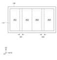
도 4는 셀 웨이퍼(CW)의 메모리 셀 어레이(110) 배치를 나타낸 예시적인 평면도이다.Figure 4 is an exemplary plan view showing the arrangement of a memory cell array (110) on a cell wafer (CW).
도 4를 참조하면, 메모리 셀 어레이(110)는 제1 메모리 그룹(MG1) 내지 제4 메모리 그룹(MG4)으로 분리될 수 있다. 제1 메모리 그룹(MG1)과 제2 메모리 그룹(MG2)은 제1 슬리밍 영역(SR1)의 제1 방향(FD) 양측에 배치될 수 있고, 제3 메모리 그룹(MG3)과 제4 메모리 그룹(MG4)은 제2 슬리밍 영역(SR2)의 제1 방향(FD) 양측에 배치될 수 있다.Referring to FIG. 4, the memory cell array (110) can be divided into a first memory group (MG1) to a fourth memory group (MG4). The first memory group (MG1) and the second memory group (MG2) can be arranged on both sides of the first direction (FD) of the first slimming region (SR1), and the third memory group (MG3) and the fourth memory group (MG4) can be arranged on both sides of the first direction (FD) of the second slimming region (SR2).
이와 같이, 메모리 셀 어레이(110)는 슬리밍 영역 개수의 두 배의 메모리 그룹들(MG1 내지 MG4)로 분리되며, 두 개의 메모리 그룹들은 쌍을 이루어 대응되는 하나의 슬리밍 영역의 제1 방향(FD) 양측에 각각 배치될 수 있다.In this way, the memory cell array (110) is divided into memory groups (MG1 to MG4) twice the number of slimming regions, and two memory groups can be arranged in pairs on each side of the first direction (FD) of a corresponding slimming region.
도시하지 않았지만, 제1 메모리 그룹(MG1) 내지 제4 메모리 그룹(MG4) 각각은 복수개의 비트 라인들을 포함할 수 있다.Although not shown, each of the first memory group (MG1) to the fourth memory group (MG4) may include multiple bit lines.
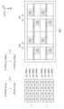
도 5는 제1 페리 웨이퍼(PW1)의 페이지 버퍼 저전압 회로(132) 배치를 나타낸 예시적인 평면도이다.FIG. 5 is an exemplary plan view showing the arrangement of a page buffer low-voltage circuit (132) of a first ferry wafer (PW1).
도 5를 참조하면, 페이지 버퍼 저전압 회로(132)는 매트릭스 형태로 배열된 복수의 페이지 버퍼 저전압 유닛들(LV)을 포함할 수 있다. 페이지 버퍼 저전압 회로(132)의 행의 개수는 데이터 입출력 핀의 개수와 동일할 수 있다. 예시적으로, 데이터 입출력 핀이 8개인 경우 페이지 버퍼 저전압 회로(132)는 8개의 행(row)으로 구성될 수 있고, 페이지 버퍼 저전압 회로(132)의 각 열(column)에는 8개의 페이지 버퍼 저전압 유닛들(LV)이 배치될 수 있다.Referring to FIG. 5, the page buffer low voltage circuit (132) may include a plurality of page buffer low voltage units (LV) arranged in a matrix form. The number of rows of the page buffer low voltage circuit (132) may be equal to the number of data input/output pins. For example, when there are eight data input/output pins, the page buffer low voltage circuit (132) may be configured with eight rows, and eight page buffer low voltage units (LV) may be arranged in each column of the page buffer low voltage circuit (132).
다만, 본 실시예가 이로 한정되는 것은 아니고, 페이지 버퍼 저전압 회로(132)의 행의 개수와 데이터 입출력 핀의 개수가 다른 경우에도 적용될 수 있다. 본 명세서에서, 행의 개수는 스테이지(stage) 개수와 동일한 개념인 것으로 사용될 것이다.However, the present embodiment is not limited thereto, and may be applied even when the number of rows of the page buffer low voltage circuit (132) and the number of data input/output pins are different. In this specification, the number of rows will be used as the same concept as the number of stages.
페이지 버퍼 저전압 회로(132)는 제1 내지 제8 페이지 버퍼 저전압 그룹(PB LV Group 1 내지 PB LV Group 8)으로 분리될 수 있다. 이러한 경우, 페이지 버퍼 저전압 회로(132)에 포함된 복수의 페이지 버퍼 저전압 유닛들(LV)이 8개의 페이지 버퍼 저전압 그룹(PB LV Group 1 내지 PB LV Group 8)으로 그룹화된 것으로 이해될 수 있다.The page buffer low voltage circuit (132) can be divided into first to eighth page buffer low voltage groups (
제2 방향(SD)을 따라서 일렬로 배치되는 제1 페이지 버퍼 저전압 그룹(PB LV Group 1)과 제2 페이지 버퍼 저전압 그룹(PB LV Group 2)은 제1 메모리 그룹(도 4의 MG1)에 대응되고, 제1 메모리 그룹(도 4의 MG1)과 수직 방향(VD)으로 중첩될 수 있다. 제2 방향(SD)을 따라서 일렬로 배치되는 제3 페이지 버퍼 저전압 그룹(PB LV Group 3)과 제4 페이지 버퍼 저전압 그룹(PB LV Group 4)은 제2 메모리 그룹(도 4의 MG2)에 대응되고, 제2 메모리 그룹(도 4의 MG2)과 수직 방향(VD)으로 중첩될 수 있다.The first page buffer low voltage group (PB LV Group 1) and the second page buffer low voltage group (PB LV Group 2), which are arranged in a row along the second direction (SD), correspond to the first memory group (MG1 of FIG. 4) and can be vertically overlapped with the first memory group (MG1 of FIG. 4) in the VD direction. The third page buffer low voltage group (PB LV Group 3) and the fourth page buffer low voltage group (PB LV Group 4), which are arranged in a row along the second direction (SD), correspond to the second memory group (MG2 of FIG. 4) and can be vertically overlapped with the second memory group (MG2 of FIG. 4) in the VD direction.
제2 방향(SD)을 따라서 일렬로 배치되는 제5 페이지 버퍼 저전압 그룹(PB LV Group 5)과 제6 페이지 버퍼 저전압 그룹(PB LV Group 6)은 제3 메모리 그룹(도 4의 MG3)에 대응되고, 제3 메모리 그룹(도 4의 MG3)과 수직 방향(VD)으로 중첩될 수 있다. 제2 방향(SD)을 따라서 일렬로 배치되는 제7 페이지 버퍼 저전압 그룹(PB LV Group 7)과 제8 페이지 버퍼 저전압 그룹(PB LV Group 8)은 제4 메모리 그룹(도 4의 MG4)에 대응되고, 제4 메모리 그룹(도 4의 MG4)과 수직 방향(VD)으로 중첩될 수 있다.The fifth page buffer low voltage group (PB LV Group 5) and the sixth page buffer low voltage group (PB LV Group 6), which are arranged in a row along the second direction (SD), correspond to the third memory group (MG3 of FIG. 4) and can be vertically overlapped with the third memory group (MG3 of FIG. 4) in the VD direction. The seventh page buffer low voltage group (PB LV Group 7) and the eighth page buffer low voltage group (PB LV Group 8), which are arranged in a row along the second direction (SD), correspond to the fourth memory group (MG4 of FIG. 4) and can be vertically overlapped with the fourth memory group (MG4 of FIG. 4) in the VD direction.
페이지 버퍼 저전압 회로(132)의 페이지 버퍼 저전압 유닛들(LV)이 8개의 스테이지로 구성되고, 하나의 메모리 그룹에 대응하여 2개의 페이지 버퍼 저전압 그룹들이 제2 방향(SD)을 따라서 일렬로 배치되는 경우, 하나의 페이지 버퍼 저전압 그룹은 4개의 스테이지로 구성될 수 있다.When the page buffer low voltage units (LV) of the page buffer low voltage circuit (132) are configured with eight stages and two page buffer low voltage groups are arranged in a row along the second direction (SD) corresponding to one memory group, one page buffer low voltage group can be configured with four stages.
비록, 본 실시예에서는 페이지 버퍼 저전압 회로(132)가 메모리 그룹 개수의 두 배의 페이지 버퍼 저전압 그룹들로 분리된 경우를 나타내나, 이에 한정되는 것은 아니다. 페이지 버퍼 저전압 회로(132)는 메모리 그룹 개수의 N(N은 자연수)배의 페이지 버퍼 저전압 그룹으로 분리될 수 있다. 이러한 경우, N개의 페이지 버퍼 저전압 그룹이 하나의 메모리 그룹에 대응하고, 대응하는 하나의 메모리 그룹과 수직 방향(VD)으로 중첩되는 위치에서 제2 방향(SD)을 따라서 일렬로 배치될 수 있다.Although, in this embodiment, the page buffer low voltage circuit (132) is divided into page buffer low voltage groups twice the number of memory groups, it is not limited thereto. The page buffer low voltage circuit (132) may be divided into page buffer low voltage groups N (N is a natural number) times the number of memory groups. In this case, N page buffer low voltage groups may be arranged in a row along the second direction (SD) at a position corresponding to one memory group and overlapping with the corresponding one memory group in the vertical direction (VD).
도 4를 참조로 설명한 바와 같이, 메모리 셀 어레이(110)가 슬리밍 영역 개수의 두 배의 메모리 그룹들로 분리되며, 두 개의 메모리 그룹들이 쌍을 이루어 대응되는 하나의 슬리밍 영역의 제1 방향(FD) 양측에 각각 배치되므로, 페이지 버퍼 저전압 회로(132)는 슬리밍 영역 개수의 2N배의 페이지 버퍼 저전압 그룹으로 분리되고, 2N개의 페이지 버퍼 저전압 그룹들이 대응하는 하나의 슬리밍 영역의 제1 방향(FD) 양측에 N개씩 배치되는 것으로 볼 수 있다.As described with reference to FIG. 4, the memory cell array (110) is divided into memory groups twice the number of slimming regions, and two memory groups are arranged in pairs on both sides of the first direction (FD) of a corresponding one slimming region, so the page buffer low-voltage circuit (132) can be viewed as being divided into page buffer low-voltage groups 2N times the number of slimming regions, and 2N page buffer low-voltage groups are arranged N each on both sides of the first direction (FD) of a corresponding one slimming region.
이하, 도 6 내지 도 14를 참조로 제2 페리 웨이퍼의 패스 트랜지스터 회로 및 페이지 버퍼 고전압 회로의 다양한 배치 형태를 설명할 것이다.Hereinafter, various arrangement forms of the pass transistor circuit and the page buffer high-voltage circuit of the second ferry wafer will be described with reference to FIGS. 6 to 14.
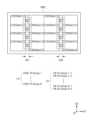
도 6 내지 도 8, 도 10 내지 도 12 및 도 14는 제2 페리 웨이퍼(PW2)의 패스 트랜지스터 회로(121) 및 페이지 버퍼 고전압 회로(131) 배치를 나타낸 예시적인 평면도들이고, 도 9는 도 8에 도시된 한 쌍의 페이지 버퍼 고전압 그룹들과 이들에 대응하는 하나의 페이지 버퍼 저전압 그룹의 배치를 나타낸 도면이고, 도 13은 도 12에 도시된 하나의 페이지 버퍼 고전압 그룹과 이에 대응하는 하나의 페이지 버퍼 저전압 그룹의 배치를 나타낸 도면이다.FIGS. 6 to 8, FIGS. 10 to 12, and FIG. 14 are exemplary plan views showing the arrangement of a pass transistor circuit (121) and a page buffer high-voltage circuit (131) of a second ferry wafer (PW2), FIG. 9 is a drawing showing the arrangement of a pair of page buffer high-voltage groups shown in FIG. 8 and a corresponding page buffer low-voltage group, and FIG. 13 is a drawing showing the arrangement of a page buffer high-voltage group shown in FIG. 12 and a corresponding page buffer low-voltage group.
도 6을 참조하면, 패스 트랜지스터 회로(121)는 제1 내지 제8 패스 트랜지스터 그룹(PASS TR Group 1 내지 PASS TR Group 8)으로 분리될 수 있다. 이러한 경우, 패스 트랜지스터 회로(121)에 포함된 복수의 패스 트랜지스터들이 8개의 패스 트랜지스터 그룹들(PASS TR Group 1 내지 PASS TR Group 8)로 분리된 것으로 이해될 수 있다.Referring to FIG. 6, the pass transistor circuit (121) can be divided into first to eighth pass transistor groups (
제1 슬리밍 영역(SR1) 및 제2 슬리밍 영역(SR2)에 워드 라인들의 패드 영역들(도 3의 LP)이 위치할 수 있다. 제1 내지 제4 패스 트랜지스터 그룹(PASS TR Group 1 내지 PASS TR Group 4)은 제1 슬리밍 영역(SR1)과 인접한 위치에 배치되며, 제1 내지 제4 패스 트랜지스터 그룹(PASS TR Group 1 내지 PASS TR Group 4)의 패스 트랜지스터들은 제1 슬리밍 영역(SR1)에 배치된 패드 영역들에 각각 연결될 수 있다. 본 실시예에서, 제1 내지 제4 패스 트랜지스터 그룹(PASS TR Group 1 내지 PASS TR Group 4)은 제1 슬리밍 영역(SR1)을 중심으로 워드 라인들의 나열 방향인 제2 방향(SD)을 따라서 지그재그 형태로 배열된다.Pad regions (LP of FIG. 3) of word lines may be positioned in the first slimming region (SR1) and the second slimming region (SR2). The first to fourth pass transistor groups (
제5 내지 제8 패스 트랜지스터 그룹(PASS TR Group 5 내지 PASS TR Group 8)은 제2 슬리밍 영역(SR2)과 인접한 위치에 배치되며, 제5 내지 제8 패스 트랜지스터 그룹(PASS TR Group 5 내지 PASS TR Group 8)의 패스 트랜지스터들은 제2 슬리밍 영역(SR2)에 배치된 패드 영역들(도 3의 LP)에 각각 연결될 수 있다. 본 실시예에서, 제5 내지 제8 패스 트랜지스터 그룹(PASS TR Group 5 내지 PASS TR Group 8)은 제2 슬리밍 영역(SR2)을 중심으로 워드 라인들의 나열 방향인 제2 방향(SD)을 따라서 지그재그 형태로 배열된다.The fifth to eighth pass transistor groups (
비록, 본 실시예에서는 패스 트랜지스터 회로(121)가 슬리밍 영역 개수의 4배의 패스 트랜지스터 그룹으로 분리되는 경우를 나타내나, 이에 한정되는 것은 아니다. 패스 트랜지스터 회로(121)는 페이지 버퍼 저전압 그룹의 개수와 동일한 개수, 즉 슬리밍 영역 개수의 2N배의 패스 트랜지스터 그룹으로 분리될 수 있다.Although, in this embodiment, the pass transistor circuit (121) is divided into four pass transistor groups as many as the number of slimming regions, it is not limited thereto. The pass transistor circuit (121) may be divided into the same number of pass transistor groups as the number of page buffer low-voltage groups, that is, 2N times the number of slimming regions.
페이지 버퍼 고전압 회로(131)는 페이지 버퍼 저전압 그룹 개수와 동일한 개수의 페이지 버퍼 고전압 그룹(PB HV Group 1 내지 PB HV Group 8)으로 분리될 수 있고, 각 페이지 버퍼 고전압 그룹은 대응하는 하나의 페이지 버퍼 저전압 그룹과 수직 방향(VD)으로 중첩하여 배치될 수 있다. 이러한 경우, 페이지 버퍼 고전압 그룹의 스테이지 개수는 하나의 페이지 버퍼 저전압 그룹의 스테이지 개수와 동일할 수 있다.The page buffer high voltage circuit (131) can be divided into a number of page buffer high voltage groups (
본 실시예는, 페이지 버퍼 고전압 회로(131)가 제1 내지 제8 페이지 버퍼 저전압 그룹(PB LV Group 1 내지 PB HV Group 8)에 각각 대응하여 제1 내지 제8 페이지 버퍼 고전압 그룹(PB HV Group 1 내지 PB HV Group 8)으로 분리된 경우를 나타낸다.This embodiment shows a case where the page buffer high voltage circuit (131) is divided into the first to eighth page buffer high voltage groups (
제1,제2 페이지 버퍼 고전압 그룹(PB HV Group 1,2)은 제1 메모리 그룹(도 4의 MG1)의 비트 라인들에 연결될 수 있다. 제1 페이지 버퍼 고전압 그룹(PB HV Group 1)은 연결 라인들을 통해서 제1 페이지 버퍼 저전압 그룹(도 5의 PB LV Group 1)에 연결될 수 있고, 제2 페이지 버퍼 고전압 그룹(PB HV Group 2)은 연결 라인들을 통해서 제2 페이지 버퍼 저전압 그룹(도 5의 PB LV Group 2)에 연결될 수 있다.The first and second page buffer high voltage groups (
제3,제4 페이지 버퍼 고전압 그룹(PB HV Group 3,4)은 제2 메모리 그룹(도 4의 MG2)의 비트 라인들에 연결될 수 있다. 제3 페이지 버퍼 고전압 그룹(PB HV Group 3)은 연결 라인들을 통해서 제3 페이지 버퍼 저전압 그룹(도 5의 PB LV Group 3)에 연결될 수 있고, 제4 페이지 버퍼 고전압 그룹(PB HV Group 4)은 연결 라인들을 통해서 제4 페이지 버퍼 저전압 그룹(도 5의 PB LV Group 4)에 연결될 수 있다.The third and fourth page buffer high voltage groups (
제5,제6 페이지 버퍼 고전압 그룹(PB HV Group 5,6)은 제3 메모리 그룹(도 4의 MG3)의 비트 라인들에 연결될 수 있다. 제5 페이지 버퍼 고전압 그룹(PB HV Group 5)은 연결 라인들을 통해서 제5 페이지 버퍼 저전압 그룹(도 5의 PB LV Group 5)에 연결될 수 있고, 제6 페이지 버퍼 고전압 그룹(PB HV Group 6)은 연결 라인들을 통해서 제6 페이지 버퍼 저전압 그룹(도 5의 PB LV Group 6)에 연결될 수 있다.The fifth and sixth page buffer high voltage groups (
제7,제8 페이지 버퍼 고전압 그룹(PB HV Group 7,8)은 제4 메모리 그룹(도 4의 MG4)의 비트 라인들에 연결될 수 있다. 제7 페이지 버퍼 고전압 그룹(PB HV Group 7)은 연결 라인들을 통해서 제7 페이지 버퍼 저전압 그룹(도 5의 PB LV Group 7)에 연결될 수 있고, 제8 페이지 버퍼 고전압 그룹(PB HV Group 8)은 연결 라인들을 통해서 제8 페이지 버퍼 저전압 그룹(도 5의 PB LV Group 8)에 연결될 수 있다.The seventh and eighth page buffer high voltage groups (
제1 페이지 버퍼 고전압 그룹(PB HV Group 1)은 제1 메모리 그룹(도 4의 MG1) 및 제1 페이지 버퍼 저전압 그룹(도 5의 PB LV Group 1)과 수직 방향(VD)으로 중첩되며, 비트 라인들이 나열되는 방향인 제1 방향(FD)으로 긴 형태로 배치될 수 있다. 제1 페이지 버퍼 고전압 그룹(PB HV Group 1)의 제1 방향(FD) 길이는 제1 메모리 그룹(도 4의 MG1)의 제1 방향(FD) 길이 및 제1 페이지 버퍼 저전압 그룹(도 5의 PB LV Group 1)의 제1 방향(FD) 길이와 실질적으로 동일할 수 있다.The first page buffer high voltage group (PB HV Group 1) may be vertically overlapped with the first memory group (MG1 of FIG. 4) and the first page buffer low voltage group (
제2 내지 제 8 페이지 버퍼 고전압 그룹(PB HV Group 2 내지 PB HV Group 8)도 제1 페이지 버퍼 고전압 그룹(PB HV Group 1)과 유사한 형태로 구성 및 배치될 수 있다.The second to eighth page buffer high voltage groups (
하나의 패스 트랜지스터 그룹의 제2 방향(SD) 길이는 하나의 페이지 버퍼 저전압 그룹의 제2 방향(SD) 길이보다 작고, 하나의 페이지 버퍼 고전압 그룹의 제2 방향(SD) 길이는 하나의 페이지 버퍼 저전압 그룹의 제2 방향(SD) 길이보다 작다.The second direction (SD) length of one pass transistor group is smaller than the second direction (SD) length of one page buffer low-voltage group, and the second direction (SD) length of one page buffer high-voltage group is smaller than the second direction (SD) length of one page buffer low-voltage group.
이처럼, 패스 트랜지스터 회로(121)를 페이지 버퍼 저전압 그룹의 제2 방향(SD) 길이보다 작은 제2 방향(SD) 길이를 갖는 복수의 패스 트랜지스터 그룹들로 분리하여 배치하고, 페이지 버퍼 고전압 회로(131)를 페이지 버퍼 저전압 그룹의 제2 방향(SD) 길이보다 작은 제2 방향(SD) 길이를 갖는 복수의 페이지 버퍼 고전압 그룹들로 분리하여 배치함으로써, 패스 트랜지스터 그룹들과 페이지 버퍼 고전압 그룹들을 서로 간섭됨 없이 하나의 평면에 배치할 수 있다.In this way, by dividing and arranging the pass transistor circuit (121) into a plurality of pass transistor groups having a second direction (SD) length smaller than the second direction (SD) length of the page buffer low voltage group, and dividing and arranging the page buffer high voltage circuit (131) into a plurality of page buffer high voltage groups having a second direction (SD) length smaller than the second direction (SD) length of the page buffer low voltage group, the pass transistor groups and the page buffer high voltage groups can be arranged on a single plane without interfering with each other.
도 7을 참조하면, 제1 내지 제4 패스 트랜지스터 그룹(PASS TR Group 1 내지 PASS TR Group 4)은 제1 슬리밍 영역(SR1)을 중심으로 제2 방향(SD)을 따라서 지그재그 형태로 배치되되, 각 패스 트랜지스터 그룹(PASS TR Group 1 내지 PASS TR Group 4)의 적어도 일부분은 제1 슬리밍 영역(SR1) 내부에 위치될 수 있다.Referring to FIG. 7, the first to fourth pass transistor groups (
제5 내지 제8 패스 트랜지스터 그룹(PASS TR Group 5 내지 PASS TR Group 8)은 제2 슬리밍 영역(SR2)을 중심으로 제2 방향(SD)을 따라서 지그재그 형태로 배치되되, 각 패스 트랜지스터 그룹(PASS TR Group 5 내지 PASS TR Group 8) 의 적어도 일부분은 제2 슬리밍 영역(SR2) 내부에 위치될 수 있다.The fifth to eighth pass transistor groups (
본 실시예는 패스 트랜지스터 그룹의 제1 방향(FD) 폭이 슬리밍 영역의 제1 방향(FD) 폭보다 큰 경우를 나타낸 것으로, 패스 트랜지스터 그룹의 제1 방향(FD) 폭이 슬리밍 영역의 제1 방향(FD) 폭과 동일하거나 이보다 작은 경우, 패스 트랜지스터 그룹 전체가 대응하는 슬리밍 영역 내부에 배치될 수도 있다.This embodiment shows a case where the first direction (FD) width of the pass transistor group is larger than the first direction (FD) width of the slimming region. If the first direction (FD) width of the pass transistor group is equal to or smaller than the first direction (FD) width of the slimming region, the entire pass transistor group may be placed inside the corresponding slimming region.
이와 같이, 패스 트랜지스터 그룹들(PASS TR Group 1 내지 PASS TR Group 8)의 적어도 일부가 슬리밍 영역 내부에 배치되는 경우, 패스 트랜지스터 그룹들(PASS TR Group 1 내지 PASS TR Group 8) 전체가 슬리밍 영역 외부에 배치되는 경우와 비교해서, 페이지 버퍼 고전압 그룹들(PB HV Group 1 내지 PB HV Group 8) 및 패스 트랜지스터 그룹들(PASS TR Group 1 내지 PASS TR Group 8)의 배치에 활용되지 않는 연속적인 영역(십자가 해칭 부분)의 면적이 증가될 것이다. 이러한 영역에 주변 회로(도 1의 140)가 배치될 수 있다.In this way, when at least some of the pass transistor groups (
주변 회로에 포함된 회로들 중에서 상대적으로 넓은 연속적인 공간에 배치될 필요가 있는 회로가 있을 수 있다. 이러한 회로는 메모리 셀 어레이(도 4의 110)와 수직 방향(VD)으로 중첩되지 않는 부분을 가질 수 있다. 이에 따라, 제2 페리 웨이퍼(PW2)의 면적이 증가하고 메모리 장치의 사이즈가 커질 수 있다.Among the circuits included in the peripheral circuit, there may be a circuit that needs to be placed in a relatively wide continuous space. Such a circuit may have a portion that does not overlap with the memory cell array (110 in FIG. 4) in the vertical direction (VD). Accordingly, the area of the second peripheral wafer (PW2) may increase and the size of the memory device may increase.
본 실시예에 의하면, 각 패스 트랜지스터 그룹의 적어도 일부분이 슬리밍 영역 내부에 위치되므로, 페이지 버퍼 고전압 그룹들(PB HV Group 1 내지 PB HV Group 8) 및 패스 트랜지스터 그룹들(PASS TR Group 1 내지 PASS TR Group 8)의 배치에 활용되지 않는 넓은 연속적인 영역을 제공할 수 있고, 이러한 영역에 주변 회로를 배치함으로써 제2 페리 웨이퍼(PW2)의 면적을 줄일 수 있다.According to the present embodiment, since at least a portion of each pass transistor group is located within the slimming region, a wide continuous region that is not utilized for the placement of the page buffer high-voltage groups (
도 8을 참조하면, 페이지 버퍼 고전압 회로(131)는 페이지 버퍼 저전압 그룹 개수의 두 배의 페이지 버퍼 고전압 그룹(PB HV Group 1-1 내지 PB HV Group 8-2)으로 분리될 수 있다. 두 개의 페이지 버퍼 고전압 그룹들이 쌍을 이루어 대응하는 하나의 페이지 버퍼 저전압 그룹과 수직 방향(VD)으로 중첩되며 제2 방향(SD)으로 간격을 갖고 서로 분리되어 배치될 수 있다.Referring to FIG. 8, the page buffer high voltage circuit (131) can be divided into twice the number of page buffer high voltage groups (PB HV Group 1-1 to PB HV Group 8-2) as the number of page buffer low voltage groups. Two page buffer high voltage groups can be arranged in pairs so as to overlap with a corresponding one page buffer low voltage group in the vertical direction (VD) and be separated from each other with a gap in the second direction (SD).
이러한 경우, 하나의 페이지 버퍼 고전압 그룹의 스테이지 개수는, 하나의 페이지 버퍼 저전압 그룹의 스테이지 개수의 절반일 수 있다. 예시적으로, 하나의 페이지 버퍼 저전압 그룹이 4개의 스테이지로 구성된 경우, 페이지 버퍼 고전압 그룹들(PB HV Group 1-1 내지 PB HV Group 8-2) 각각은 2개의 스테이지로 구성될 수 있다.In this case, the number of stages of one page buffer high-voltage group may be half of the number of stages of one page buffer low-voltage group. For example, if one page buffer low-voltage group consists of four stages, each of the page buffer high-voltage groups (PB HV Group 1-1 to PB HV Group 8-2) may consist of two stages.
도 9를 참조하면, 페이지 버퍼 고전압 유닛(HV)의 제2 방향(SD) 길이는 L1으로, 페이지 버퍼 저전압 유닛(LV)의 제2 방향(SD) 길이인 L2보다 짧다. L1과 L2간 차이로 인하여, 연결 라인을 통해서 서로 연결되는 페이지 버퍼 고전압 유닛(HV)과 페이지 버퍼 저전압 유닛(LV)이 제2 방향(SD)으로 서로 떨어져 배치될 수 있다.Referring to FIG. 9, the second direction (SD) length of the page buffer high voltage unit (HV) is L1, which is shorter than the second direction (SD) length of the page buffer low voltage unit (LV) is L2. Due to the difference between L1 and L2, the page buffer high voltage unit (HV) and the page buffer low voltage unit (LV), which are connected to each other through a connection line, can be arranged apart from each other in the second direction (SD).
예를 들어, 박스 A 안의 페이지 버퍼 고전압 유닛(HV)과 박스 B 안의 페이지 버퍼 저전압 유닛(LV)은 연결 라인을 통해서 서로 연결될 수 있고, 제2 방향(SD)으로 d1만큼 떨어져 배치될 수 있다.For example, a page buffer high voltage unit (HV) in box A and a page buffer low voltage unit (LV) in box B can be connected to each other through a connection line and can be arranged at a distance d1 apart in the second direction (SD).
본 실시예와 다르게, PB HV GROUP 7-1이 PB HV GROUP 7-2와 분리되지 않고 PB HV GROUP 7-2에 접하여 배치되는 경우 d1의 크기가 커지게 되어, 박스 A 안의 페이지 버퍼 고전압 유닛(HV)과 박스 B 안의 페이지 버퍼 저전압 유닛(LV)을 연결하는데 긴 길이의 연결 라인을 사용해야 할 것이다.Unlike the present embodiment, if PB HV GROUP 7-1 is not separated from PB HV GROUP 7-2 but is placed in contact with PB HV GROUP 7-2, the size of d1 becomes larger, so that a long connection line must be used to connect the page buffer high voltage unit (HV) in box A and the page buffer low voltage unit (LV) in box B.
도 8의 실시예에 의하면, 하나의 페이지 버퍼 저전압 그룹(ex, 도 5의 PB LV GROUP 7)에 대응하는 두 개의 페이지 버퍼 고전압 그룹들(ex, PB HV GROUP 7-1, PB HV GROUP 7-2)이 제2 방향(SD)으로 간격을 갖고 서로 분리되어 배치되므로, 대응하는 페이지 버퍼 고전압 유닛(HV)과 페이지 버퍼 저전압 유닛(LV)간 간격을 줄일 수 있고 대응하는 페이지 버퍼 고전압 유닛(HV)과 페이지 버퍼 저전압 유닛(LV)을 연결하는데 사용되는 연결 라인의 길이를 단축시킬 수 있다.According to the embodiment of FIG. 8, two page buffer high voltage groups (e.g., PB HV GROUP 7-1, PB HV GROUP 7-2) corresponding to one page buffer low voltage group (e.g.,
도 10을 참조하면, 제1 내지 제8 패스 트랜지스터 그룹(PASS TR Group 1 내지 PASS TR Group 8)은 제1 슬리밍 영역(SR1), 제2 슬리밍 영역(SR2), 그리고 제1 슬리밍 영역(SR1)과 제2 슬리밍 영역(SR2) 사이의 셀 영역(CR)에 배치되지 않고, 이들 영역의 바깥에 배치될 수 있다.Referring to FIG. 10, the first to eighth pass transistor groups (
구체적으로, 제1 내지 제4 패스 트랜지스터 그룹(PASS TR Group 1 내지 PASS TR Group 4)은 제1 슬리밍 영역(SR1)을 기준으로 셀 영역(CR)의 반대측 영역에 일렬로 배치될 수 있고, 제5 내지 제8 패스 트랜지스터 그룹(PASS TR Group 5 내지 PASS TR Group 8)은 제2 슬리밍 영역(SR2)을 기준으로 셀 영역(CR)의 반대측 영역에 일렬로 배치될 수 있다. 이러한 경우, 제1 내지 제4 패스 트랜지스터 그룹(PASS TR Group 1 내지 PASS TR Group 4)과 제5 내지 제8 패스 트랜지스터 그룹(PASS TR Group 5 내지 PASS TR Group 8)은 제1 슬리밍 영역(SR1), 셀 영역(CR), 제2 슬리밍 영역(SR2)을 사이에 두고 서로 떨어져 배치될 것이다.Specifically, the first to fourth pass transistor groups (
이와 같이 패스 트랜지스터 그룹들(PASS TR Group 1 내지 PASS TR Group 8)이 제1 방향(FD)을 따라서 연속적으로 위치하는 제1 슬리밍 영역(SR), 셀 영역(CR) 및 제2 슬리밍 영역(SR2)의 바깥에 배치되므로, 페이지 버퍼 고전압 그룹들(PB HV Group 1 내지 PB HV Group 8) 및 패스 트랜지스터 그룹들(PASS TR Group 1 내지 PASS TR Group 8)의 배치에 활용되지 않는 상대적으로 넓은 연속적인 영역이 제공될 수 있다. 이러한 영역에 상대적으로 넓은 연속적인 공간에 배치될 필요가 있는 주변 회로가 배치될 수 있다. 따라서, 주변 회로로 인한 제2 페리 웨이퍼(PW2)의 면적 증가가 억제될 수 있다.In this way, since the pass transistor groups (
도 11을 참조하면, 제1 내지 제4 패스 트랜지스터 그룹(PASS TR Group 1 내지 PASS TR Group 4)은 제2 방향(SD)을 따라서 일렬로 배치되며, 제1 내지 제4 패스 트랜지스터 그룹(PASS TR Group 1 내지 PASS TR Group 4)의 제1 방향(FD) 중심부는 제1 슬리밍 영역(SR1)의 제1 방향(FD) 중심부와 얼라인될 수 있다.Referring to FIG. 11, the first to fourth pass transistor groups (
제5 내지 제8 패스 트랜지스터 그룹(PASS TR Group 5 내지 PASS TR Group 8)은 제2 방향(SD)을 따라서 일렬로 배치되며, 제5 내지 제8 패스 트랜지스터 그룹(PASS TR Group 5 내지 PASS TR Group 8)의 제1 방향(FD) 중심부는 제2 슬리밍 영역(SR2)의 제1 방향(FD) 중심부와 얼라인될 수 있다.The fifth to eighth pass transistor groups (
앞서, 도 6을 참조로 하여 설명한 바와 같이, 제1 내지 제4 패스 트랜지스터 그룹(PASS TR Group 1 내지 PASS TR Group 4)의 패스 트랜지스터들이 제1 슬리밍 영역(SR1)의 패드 영역들에 각각 연결되므로, 패스 트랜지스터와 이에 대응하는 패드 영역을 연결하는데 사용되는 배선의 길이를 짧게 구성하기 위해서는 패스 트랜지스터를 제1 슬리밍 영역(SR1) 내부에 배치하거나 또는 패스 트랜지스터를 제1 슬리밍 영역(SR1) 외부에 배치할 경우 패스 트랜지스터와 제1 슬리밍 영역(SR1)간 간격을 최대한 줄여야 할 것이다.As described above with reference to FIG. 6, since the pass transistors of the first to fourth pass transistor groups (
제1 내지 제4 패스 트랜지스터 그룹(PASS TR Group 1 내지 PASS TR Group 4)의 제1 방향(FD) 폭은, 제1 내지 제4 패스 트랜지스터 그룹(PASS TR Group 1 내지 PASS TR Group 4)에 포함된 패스 트랜지스터들이 점유하는 영역의 제1 방향(FD) 폭에 해당할 수 있다.The first direction (FD) width of the first to fourth pass transistor groups (
워드 라인들의 개수가 늘어남에 따라서 제1 내지 제4 패스 트랜지스터 그룹(PASS TR Group 1 내지 PASS TR Group 4)에 포함된 패스 트랜지스터들의 개수가 많아 지고, 제1 내지 제4 패스 트랜지스터 그룹(PASS TR Group 1 내지 PASS TR Group 4)의 패스 트랜지스터들이 점유하는 영역의 제1 방향(FD) 폭, 다시 말해서 제1 내지 제4 패스 트랜지스터 그룹(PASS TR Group 1 내지 PASS TR Group 4)의 제1 방향(FD) 폭이 늘어나게 되어, 제1 내지 제4 패스 트랜지스터 그룹(PASS TR Group 1 내지 PASS TR Group 4)의 제1 방향(FD) 폭이 제1 슬리밍 영역(SR1)의 제1 방향(FD) 폭보다 커질 수 있다. 이러한 경우, 제1 내지 제4 패스 트랜지스터 그룹(PASS TR Group 1 내지 PASS TR Group 4)에 포함된 모든 트랜지스터들을 제1 슬리밍 영역(SR1) 내부에 배치하는 것이 불가능하며 일부 패스 트랜지스터들은 제1 슬리밍 영역(SR1) 외부에 배치될 것이다.As the number of word lines increases, the number of pass transistors included in the first to fourth pass transistor groups (
본 실시예와 다르게, 제1 내지 제4 패스 트랜지스터 그룹(PASS TR Group 1 내지 PASS TR Group 4)이 제1 슬리밍 영역(SR1)의 중심부를 기준으로 어느 한쪽 방향으로 치우쳐서 배치되는 경우, 제1 슬리밍 영역(SR1)으로부터 멀어지는 방향으로 치우친 쪽에 위치하는 패스 트랜지스터를 패드 영역에 연결하기 위해서는 긴 길이의 배선을 사용해야 할 것이다. 배선의 길이가 길어지면 RC 딜레이가 커지게 되어 메모리 장치의 성능이 저하될 수 있다.Unlike the present embodiment, if the first to fourth pass transistor groups (
본 발명의 실시예에 의하면, 제1 내지 제4 패스 트랜지스터 그룹(PASS TR Group 1 내지 PASS TR Group 4)의 제1 방향(FD) 중심부가 제1 슬리밍 영역(SR1)의 제1 방향(FD) 중심부와 얼라인되므로, 제1 내지 제4 패스 트랜지스터 그룹(PASS TR Group 1 내지 PASS TR Group 4)이 제1 슬리밍 영역(SR1)을 중심으로 어느 한쪽으로 치우치지 않고 배치되며, 이에 따라 제1 슬리밍 영역(SR1)과 가장 멀리 떨어져 있는 패스 트랜지스터와 제1 슬리밍 영역(SR1) 간 거리가 단축되어 패스 트랜지스터와 제1 슬리밍 영역(SR1)에 위치하는 패드 영역을 연결하는데 사용되는 배선의 길이를 줄이는 것이 가능하다.According to an embodiment of the present invention, since the first direction (FD) center of the first to fourth pass transistor groups (
도 12를 참조하면, 제1 내지 제8 페이지 버퍼 고전압 그룹(PB HV Group 1 내지 PB HV Group 8) 각각의 제2 방향(SD) 중심부는 대응하는 페이지 버퍼 저전압 그룹의 제2 방향(SD) 중심부와 얼라인될 수 있다. 예시적으로, 제1 페이지 버퍼 고전압 그룹(PB HV Group 1)의 제2 방향(SD) 중심부는 제1 페이지 버퍼 저전압 그룹(도 5의 PB LV Group 1)의 제2 방향(SD) 중심부와 얼라인될 수 있다.Referring to FIG. 12, the second direction (SD) center of each of the first to eighth page buffer high voltage groups (
도 13을 참조하면, 페이지 버퍼 고전압 유닛(HV)의 제2 방향(SD) 길이(L1)와 페이지 버퍼 저전압 유닛(LV)의 제2 방향(SD) 길이(L2)가 서로 다름으로 인하여, 연결 라인을 통해서 서로 연결되는 페이지 버퍼 고전압 유닛(HV)과 페이지 버퍼 저전압 유닛(LV)이 제2 방향(SD)으로 서로 떨어져 배치될 수 있다.Referring to FIG. 13, since the second direction (SD) length (L1) of the page buffer high voltage unit (HV) and the second direction (SD) length (L2) of the page buffer low voltage unit (LV) are different from each other, the page buffer high voltage unit (HV) and the page buffer low voltage unit (LV), which are connected to each other through a connection line, can be arranged apart from each other in the second direction (SD).
예를 들어, 박스 A 안의 페이지 버퍼 고전압 유닛(HV)과 박스 B 안의 페이지 버퍼 저전압 유닛(LV)은 연결 라인을 통해서 서로 연결될 수 있고, 제2 방향(SD)으로 d2만큼 떨어져 배치될 수 있다.For example, a page buffer high voltage unit (HV) in box A and a page buffer low voltage unit (LV) in box B can be connected to each other through a connection line and can be arranged at a distance d2 apart in the second direction (SD).
본 실시예와 다르게, PB HV GROUP 7이 PB LV Group 7의 제2 방향(SD) 하단 가장자리에 얼라인되어 배치되는 경우, d2의 크기가 증가하여 박스 A 안의 페이지 버퍼 고전압 유닛(HV)과 박스 B 안의 페이지 버퍼 저전압 유닛(LV)을 연결하는데 긴 길이의 연결 라인을 사용해야 할 것이다.Unlike the present embodiment, if the
도 12의 실시예에 의하면, 각 페이지 버퍼 고전압 그룹의 제2 방향(SD) 중심부가 대응하는 페이지 버퍼 저전압 그룹의 제2 방향(SD) 중심부와 얼라인되므로, 대응하는 페이지 버퍼 고전압 유닛(HV)과 페이지 버퍼 저전압 유닛(LV)간 간격(d2)을 줄일 수 있고, 대응하는 페이지 버퍼 고전압 유닛(HV)과 페이지 버퍼 저전압 유닛(LV)을 연결하는데 사용되는 연결 라인의 길이를 단축시킬 수 있다.According to the embodiment of FIG. 12, since the second direction (SD) center of each page buffer high voltage group is aligned with the second direction (SD) center of the corresponding page buffer low voltage group, the gap (d2) between the corresponding page buffer high voltage unit (HV) and the page buffer low voltage unit (LV) can be reduced, and the length of the connection line used to connect the corresponding page buffer high voltage unit (HV) and the page buffer low voltage unit (LV) can be shortened.
도 14를 참조하면, 제1 내지 제8 패스 트랜지스터 그룹(PASS TR Group 1 내지 PASS TR Group 8)은 도 11을 참조로 하여 설명된 제1 내지 제8 패스 트랜지스터 그룹(PASS TR Group 1 내지 PASS TR Group 8)과 동일한 형태로 배치될 수 있다. 즉, 제1 내지 제4 패스 트랜지스터 그룹(PASS TR Group 1 내지 PASS TR Group 4)은 제2 방향(SD)을 따라서 일렬로 배치되며 제1 내지 제4 패스 트랜지스터 그룹(PASS TR Group 1 내지 PASS TR Group 4)의 제1 방향(FD) 중심부는 제1 슬리밍 영역(SR1)의 제1 방향(FD) 중심부와 얼라인되고, 제5 내지 제8 패스 트랜지스터 그룹(PASS TR Group 5 내지 PASS TR Group 8)은 제2 방향(SD)을 따라서 일렬로 배치되며, 제5 내지 제8 패스 트랜지스터 그룹(PASS TR Group 5 내지 PASS TR Group 8)의 제1 방향(FD) 중심부는 제2 슬리밍 영역(SR2)의 제1 방향(FD) 중심부와 얼라인될 수 있다.Referring to FIG. 14, the first to eighth pass transistor groups (
제1 내지 제8 페이지 버퍼 고전압 그룹(PB HV Group 1 내지 PB HV Group 8)은 도 12를 참조로 하여 설명된 제1 내지 제8 페이지 버퍼 고전압 그룹(PB HV Group 1 내지 PB HV Group 8)과 동일한 형태로 배치될 수 있다. 즉, 제1 내지 제8 페이지 버퍼 고전압 그룹(PB HV Group 1 내지 PB HV Group 8) 각각의 제2 방향(SD) 중심부는 대응하는 페이지 버퍼 저전압 그룹의 제2 방향(SD) 중심부와 얼라인될 수 있다.The first to eighth page buffer high voltage groups (
본 실시예에 의하면, 패스 트랜지스터 그룹들(PASS TR Group 1 내지 PASS TR Group 8)과 슬리밍 영역들(SR1,SR2)의 패드 영역들간을 연결하는데 사용되는 배선들의 길이를 단축시킬 수 있고, 또한 페이지 버퍼 고전압 유닛(HV)과 페이지 버퍼 저전압 유닛(LV)을 연결하는데 사용되는 배선의 길이를 단축시키는 것이 가능하다.According to the present embodiment, it is possible to shorten the length of wirings used to connect pad areas of pass transistor groups (
도 15a는 본 발명과 관련된 메모리 장치의 배치를 나타낸 도면이고, 도 15b는 본 발명에 따른 메모리 장치의 배치를 나타낸 도면이다.FIG. 15a is a drawing showing the layout of a memory device related to the present invention, and FIG. 15b is a drawing showing the layout of a memory device according to the present invention.
도 15a는 페이지 버퍼 회로(130)가 제1 페리 웨이퍼(PW1)에 배치되고, 로우 디코더 회로(120) 및 주변 회로(140)가 제2 페리 웨이퍼(PW2)에 배치되는 경우를 나타낸다. 도면부호 120A 및 120B는 2개의 슬리밍 영역(SR)에 대응하여 분리된 로우 디코더(120)의 두 부분을 각각 나타낸다.FIG. 15A shows a case where a page buffer circuit (130) is placed on a first peripheral wafer (PW1) and a row decoder circuit (120) and peripheral circuits (140) are placed on a second peripheral wafer (PW2). Drawing
페이지 버퍼 회로(130)의 제2 방향(SD)의 길이는 H1이고, 주변 회로(140) 및 로우 디코더 회로(120)의 제2 방향(SD) 길이는 H2이며, H2는 H1보다 작다. 이러한 경우, 메모리 장치의 제2 방향(SD) 크기가 H1을 기준으로 결정되어 메모리 장치는 큰 사이즈를 갖게 될 것이다.The length of the second direction (SD) of the page buffer circuit (130) is H1, and the length of the second direction (SD) of the peripheral circuit (140) and the row decoder circuit (120) is H2, and H2 is smaller than H1. In this case, the size of the second direction (SD) of the memory device is determined based on H1, so that the memory device will have a large size.
도 15b를 참조하면, 페이지 버퍼 회로의 페이지 버퍼 고전압 회로(131)의 위치를 제2 페리 웨이퍼(PW2)로 변경하고 제1 페리 웨이퍼(PW1)에는 페이지 버퍼 저전압 회로(132)만 배치할 경우, 제1 페리 웨이퍼(PW1)에 포함된 회로의 제2 방향(SD) 길이(H1')와 제2 페리 웨이퍼(PW2)에 포함된 회로의 제2 방향(SD) 길이(H2')의 길이 차이가 감소된다. 즉, H1'과 H2'는 도 15a의 H1보다 작다. 이에 따라, 메모리 장치의 제2 방향(SD) 길이가 H1보다 작은 크기를 갖는 H1' 또는 H2'을 기준으로 결정되므로 메모리 장치의 사이즈가 감소된다.Referring to FIG. 15b, when the location of the page buffer high-voltage circuit (131) of the page buffer circuit is changed to the second peripheral wafer (PW2) and only the page buffer low-voltage circuit (132) is placed on the first peripheral wafer (PW1), the length difference between the second direction (SD) length (H1') of the circuit included in the first peripheral wafer (PW1) and the second direction (SD) length (H2') of the circuit included in the second peripheral wafer (PW2) is reduced. That is, H1' and H2' are smaller than H1 of FIG. 15a. Accordingly, since the second direction (SD) length of the memory device is determined based on H1' or H2' having a smaller size than H1, the size of the memory device is reduced.
도 16은 본 발명의 실시예에 따른 메모리 장치를 포함한 메모리 시스템을 개략적으로 도시한 블록도이다.FIG. 16 is a block diagram schematically illustrating a memory system including a memory device according to an embodiment of the present invention.
도 16을 참조하면, 본 발명의 실시예에 따른 메모리 시스템(600)은 비휘발성 메모리 장치(610) 및 메모리 컨트롤러(620)를 포함할 수 있다.Referring to FIG. 16, a memory system (600) according to an embodiment of the present invention may include a nonvolatile memory device (610) and a memory controller (620).
비휘발성 메모리 장치(610)는 앞서 설명한 메모리 장치로 구성되고, 앞서 설명한 방법으로 동작될 수 있다. 메모리 컨트롤러(620)는 비휘발성 메모리 장치(610)를 제어하도록 구성될 것이다. 비휘발성 메모리 장치(610)와 메모리 컨트롤러(620)의 결합에 의해 메모리 카드 또는 반도체 디스크 장치(Solid State Disk: SSD)로 제공될 수 있을 것이다. SRAM(621)은 프로세싱 유닛(622)의 동작 메모리로써 사용된다. 호스트 인터페이스(623)는 메모리 시스템(600)과 접속되는 호스트의 데이터 교환 프로토콜을 구비한다.The nonvolatile memory device (610) is configured as the memory device described above and can be operated in the method described above. The memory controller (620) will be configured to control the nonvolatile memory device (610). The combination of the nonvolatile memory device (610) and the memory controller (620) can be provided as a memory card or a solid state disk (SSD). The SRAM (621) is used as an operating memory of the processing unit (622). The host interface (623) has a data exchange protocol of a host connected to the memory system (600).
에러 정정 블록(624)은 비휘발성 메모리 장치(610)로부터 독출된 데이터에 포함되는 에러를 검출 및 정정한다.The error correction block (624) detects and corrects errors contained in data read from the nonvolatile memory device (610).
메모리 인터페이스(625)는 본 발명의 비휘발성 메모리 장치(610)와 인터페이싱한다. 프로세싱 유닛(622)은 메모리 컨트롤러(620)의 데이터 교환을 위한 제반 제어 동작을 수행한다.The memory interface (625) interfaces with the nonvolatile memory device (610) of the present invention. The processing unit (622) performs all control operations for data exchange of the memory controller (620).
비록 도면에는 도시되지 않았지만, 본 발명에 따른 메모리 시스템(600)은 호스트(Host)와의 인터페이싱을 위한 코드 데이터를 저장하는 ROM(미도시됨) 등이 더 제공될 수 있음은 이 분야의 통상적인 지식을 습득한 자들에게 자명하다. 비휘발성 메모리 장치(620)는 복수의 플래시 메모리 칩들로 구성되는 멀티-칩 패키지로 제공될 수도 있다Although not shown in the drawing, it is obvious to those skilled in the art that the memory system (600) according to the present invention may further be provided with a ROM (not shown) for storing code data for interfacing with a host. The nonvolatile memory device (620) may also be provided as a multi-chip package composed of a plurality of flash memory chips.
이상의 본 발명의 메모리 시스템(600)은 에러의 발생 확률이 낮은 고신뢰성의 저장 매체로 제공될 수 있다. 특히, 최근 활발히 연구되고 있는 반도체 디스크 장치(Solid State Disk: 이하 SSD)와 같은 메모리 시스템에서 본 발명의 비휘발성 메모리 장치가 구비될 수 있다. 이 경우, 메모리 컨트롤러(620)는 USB, MMC, PCI-E,SATA, PATA, SCSI, ESDI, 그리고 IDE(Integrated Drive Electronics) 등과 같은 다양한 인터페이스 프로토콜들 중 하나를 통해 외부(예를 들면,호스트)와 통신하도록 구성될 것이다.The memory system (600) of the present invention can be provided as a highly reliable storage medium with a low probability of error occurrence. In particular, the nonvolatile memory device of the present invention can be provided in a memory system such as a solid state disk (SSD) that has been actively studied recently. In this case, the memory controller (620) will be configured to communicate with the outside (e.g., a host) through one of various interface protocols such as USB, MMC, PCI-E, SATA, PATA, SCSI, ESDI, and IDE (Integrated Drive Electronics).
도 17은 본 발명의 실시예에 따른 메모리 장치를 포함한 컴퓨팅 시스템을 개략적으로 보여주는 블록도이다.FIG. 17 is a block diagram schematically showing a computing system including a memory device according to an embodiment of the present invention.
도 17을 참조하면, 본 발명에 따른 컴퓨팅 시스템(700)은 시스템 버스(760)에 전기적으로 연결된 메모리 시스템(710), 마이크로프로세서(720), 램(730), 사용자 인터페이스(740), 베이스밴드 칩셋(Baseband chipset)과 같은 모뎀(750)을 포함할 수 있다 본 발명에 따른 컴퓨팅 시스템(700)이 모바일 장치인 경우, 컴퓨팅 시스템(700)의 동작 전압을 공급하기 위한 배터리(미도시됨)가 추가적으로 제공될 것이다. 비록 도면에는 도시되지 않았지만, 본 발명에 따른 컴퓨팅 시스템(700)에는 응용 칩셋(Application chipset), 카메라 이미지 프로세서(Camera Image Processor: CIS), 모바일 디램, 등이 더 제공될 수 있음은 이 분야의 통상적인 지식을 습득한 자들에게 자명하다. 메모리 시스템(710)은, 예를 들면, 데이터를 저장하는 데 비휘발성 메모리를 사용하는 SSD(Solid State Drive/Disk)를 구성할 수 있다. 또는, 메모리 시스템(710)은, 퓨전 플래시 메모리(예를 들면, 원낸드 플래시 메모리)로 제공될 수 있다.Referring to FIG. 17, a computing system (700) according to the present invention may include a memory system (710), a microprocessor (720), a RAM (730), a user interface (740), and a modem (750) such as a baseband chipset, all of which are electrically connected to a system bus (760). If the computing system (700) according to the present invention is a mobile device, a battery (not shown) for supplying an operating voltage of the computing system (700) may be additionally provided. Although not shown in the drawing, it will be apparent to those skilled in the art that the computing system (700) according to the present invention may further include an application chipset, a camera image processor (CIS), a mobile DRAM, and the like. The memory system (710) may, for example, configure an SSD (Solid State Drive/Disk) that uses nonvolatile memory to store data. Alternatively, the memory system (710) may be provided as a fusion flash memory (e.g., OneNAND flash memory).
이상에서 설명한 본 발명의 실시예는 장치 및 방법을 통해서만 구현이 되는 것은 아니며, 본 발명의 실시예 구성에 대응하는 기능을 실현하는 프로그램 또는 그 프로그램이 기록된 기록 매체를 통해서 구현될 수도 있으며, 이러한 구현은 앞서 설명한 실시예의 기재로부터 본 발명이 속하는 기술분야의 전문가라면 쉽게 구현할 수 있을 것이다.The embodiments of the present invention described above are not implemented only through devices and methods, but may also be implemented through a program that realizes a function corresponding to the configuration of the embodiments of the present invention or a recording medium on which the program is recorded, and such implementation will be easily implemented by a specialist in the technical field to which the present invention belongs based on the description of the embodiments described above.
앞서 설명한 본 발명의 상세한 설명에서는 본 발명의 실시예를 참조하여 설명하였지만, 해당 기술분야의 숙련된 당업자 또는 해당 기술분야에 통상의 지식을 갖는 자라면 후술 될 특허청구범위에 기재된 본 발명의 사상 및 기술 영역으로부터 벗어나지 않는 범위 내에서 본 발명을 다양하게 수정 및 변경시킬 수 있음을 이해할 수 있을 것이다.Although the detailed description of the present invention described above has been described with reference to embodiments of the present invention, it will be understood by those skilled in the art or having common knowledge in the art that various modifications and changes can be made to the present invention without departing from the spirit and technical scope of the present invention as set forth in the claims to be described later.
Claims (13)
Translated fromKorean상기 메모리 셀 어레이를 제어하며 페이지 버퍼 저전압 회로, 페이지 버퍼 고전압 회로, 로우 디코더 회로 및 주변 회로를 포함하는 로직 회로;를 포함하며,
상기 페이지 버퍼 저전압 회로는 상기 셀 웨이퍼와 수직 방향으로 중첩되는 제1 페리 웨이퍼에 배치되고,
상기 페이지 버퍼 고전압 회로, 상기 로우 디코더 회로 및 상기 주변 회로는 상기 셀 웨이퍼 및 상기 제1 페리 웨이퍼와 상기 수직 방향으로 중첩되는 제2 페리 웨이퍼에 배치되는 것을 특징으로 하는 수직형 구조를 갖는 메모리 장치.A memory cell array provided on a cell wafer and having a plurality of word lines extending in a first direction and a plurality of bit lines extending in a second direction arranged;
A logic circuit for controlling the above memory cell array and including a page buffer low-voltage circuit, a page buffer high-voltage circuit, a row decoder circuit and peripheral circuits;
The above page buffer low voltage circuit is arranged on a first ferry wafer that vertically overlaps the cell wafer,
A memory device having a vertical structure, characterized in that the page buffer high-voltage circuit, the row decoder circuit, and the peripheral circuit are arranged on the cell wafer and the first peripheral wafer and the second peripheral wafer that vertically overlaps.
상기 페이지 버퍼 저전압 회로는 상기 슬리밍 영역 개수의 2N(N은 자연수)배의 페이지 버퍼 저전압 그룹들로 분리되며, 2N개의 페이지 버퍼 저전압 그룹들이 대응하는 하나의 슬리밍 영역의 양측에 각각 N개씩 배치되는 것을 특징으로 하는 수직형 구조를 갖는 메모리 장치.In the first aspect, a plurality of slimming regions are included that are extended in the second direction and arranged along the first direction,
A memory device having a vertical structure, characterized in that the above page buffer low-voltage circuit is divided into 2N (N is a natural number) times the number of the slimming regions, and the 2N page buffer low-voltage groups are arranged N on each side of a corresponding slimming region.
상기 각 페이지 버퍼 고전압 그룹의 상기 제2 방향의 길이는 상기 각 페이지 버퍼 저전압 그룹의 상기 제2 방향의 길이보다 작은 것을 특징으로 하는 수직형 구조를 갖는 메모리 장치.In the second paragraph, the page buffer high voltage circuit is divided into a number of page buffer high voltage groups equal to the number of page buffer low voltage groups, and each of the page buffer high voltage groups is arranged to overlap with a corresponding page buffer low voltage group in the vertical direction.
A memory device having a vertical structure, characterized in that the length of the second direction of each of the page buffer high-voltage groups is smaller than the length of the second direction of each of the page buffer low-voltage groups.
두 개의 페이지 버퍼 고전압 그룹들이 쌍을 이루어 대응하는 하나의 페이지 버퍼 저전압 그룹과 상기 수직 방향으로 중첩되며, 상기 제2 방향으로 간격을 갖고 서로 분리되어 배치되는 것을 특징으로 하는 수직형 구조를 갖는 메모리 장치.In the second paragraph, the page buffer high voltage circuit is divided into page buffer high voltage groups twice the number of page buffer low voltage groups,
A memory device having a vertical structure, characterized in that two page buffer high-voltage groups are arranged in pairs and overlap each other with a corresponding one page buffer low-voltage group in the vertical direction, and are separated from each other with a gap in the second direction.
상기 패스 트랜지스터 회로는 상기 슬리밍 영역 개수의 2N(N은 자연수)배의 페이지 버퍼 저전압 그룹들로 분리되며, 2N개의 패스 트랜지스터 그룹들이 대응하는 하나의 슬리밍 영역을 따라서 배치되되,
상기 각 패스 트랜지스터 그룹의 상기 제2 방향의 길이는 상기 각 페이지 버퍼 저전압 그룹의 상기 제2 방향의 길이보다 작은 것을 특징으로 하는 수직형 구조를 갖는 메모리 장치.In the second paragraph, the row decoder circuit includes a pass transistor circuit,
The above pass transistor circuit is divided into 2N (N is a natural number) times the number of the above slimming regions into page buffer low-voltage groups, and 2N groups of pass transistors are arranged along a corresponding one slimming region.
A memory device having a vertical structure, characterized in that the length of each pass transistor group in the second direction is smaller than the length of each page buffer low-voltage group in the second direction.
상기 제1 슬리밍 영역에 대응하는 2N개의 패스 트랜지스터 그룹들과 상기 제2 슬리밍 영역에 대응하는 2N개의 패스 트랜지스터 그룹들이, 상기 제1 슬리밍 영역, 상기 제2 슬리밍 영역 및 상기 셀 영역을 사이에 두고 서로 떨어져 배치되는 것을 특징으로 하는 수직형 구조를 갖는 메모리 장치.In the sixth paragraph, the slimming regions include a first slimming region and a second slimming region adjacent to each other in the first direction with one cell region therebetween,
A memory device having a vertical structure, characterized in that 2N groups of pass transistors corresponding to the first slimming region and 2N groups of pass transistors corresponding to the second slimming region are arranged spaced apart from each other with the first slimming region, the second slimming region, and the cell region interposed therebetween.
복수의 제1 트랜지스터들을 포함하며 상기 메모리 셀 어레이를 제어하는 제1 로직 회로를 포함하는 제1 페리 웨이퍼; 및
복수의 제2 트랜지스터들을 포함하며 상기 메모리 셀 어레이를 제어하는 복수의 제2 로직 회로를 포함하는 제2 페리 웨이퍼;를 포함하며,
상기 제1 트랜지스터들의 게이트 절연층 두께의 종류가 상기 제2 트랜지스터들의 게이트 절연층 두께의 종류보다 적은 것을 특징으로 하는 수직형 구조를 갖는 메모리 장치.A cell wafer comprising a memory cell array;
A first peripheral wafer comprising a plurality of first transistors and a first logic circuit controlling the memory cell array; and
A second peripheral wafer comprising a plurality of second transistors and a plurality of second logic circuits controlling the memory cell array;
A memory device having a vertical structure, characterized in that the gate insulation layer thickness of the first transistors is smaller than the gate insulation layer thickness of the second transistors.
상기 제1 배선은 상기 제2 배선보다 비저항이 낮은 물질로 구성된 것을 특징으로 하는 수직형 구조를 갖는 메모리 장치.In the 11th paragraph, the first ferry wafer includes a first wiring, and the second ferry wafer includes a second wiring,
A memory device having a vertical structure, characterized in that the first wiring is composed of a material having lower resistivity than the second wiring.
Priority Applications (3)
| Application Number | Priority Date | Filing Date | Title |
|---|---|---|---|
| KR1020200137044AKR102801448B1 (en) | 2020-10-21 | 2020-10-21 | Memory device having vertical structure |
| US17/210,698US11398443B2 (en) | 2020-10-21 | 2021-03-24 | Memory device having logic circuit distributed across two peripheral wafer |
| CN202110489359.XACN114388004A (en) | 2020-10-21 | 2021-05-06 | Memory device with vertical structure |
Applications Claiming Priority (1)
| Application Number | Priority Date | Filing Date | Title |
|---|---|---|---|
| KR1020200137044AKR102801448B1 (en) | 2020-10-21 | 2020-10-21 | Memory device having vertical structure |
Publications (2)
| Publication Number | Publication Date |
|---|---|
| KR20220052749A KR20220052749A (en) | 2022-04-28 |
| KR102801448B1true KR102801448B1 (en) | 2025-04-29 |
Family
ID=81185651
Family Applications (1)
| Application Number | Title | Priority Date | Filing Date |
|---|---|---|---|
| KR1020200137044AActiveKR102801448B1 (en) | 2020-10-21 | 2020-10-21 | Memory device having vertical structure |
Country Status (3)
| Country | Link |
|---|---|
| US (1) | US11398443B2 (en) |
| KR (1) | KR102801448B1 (en) |
| CN (1) | CN114388004A (en) |
Families Citing this family (16)
| Publication number | Priority date | Publication date | Assignee | Title |
|---|---|---|---|---|
| KR20220034273A (en)* | 2020-09-10 | 2022-03-18 | 삼성전자주식회사 | Three-dimensional semiconductor memory device and electronic system including the same |
| KR20220056549A (en)* | 2020-10-28 | 2022-05-06 | 삼성전자주식회사 | Semiconductor devices having peripheral circuit regions on both sides of a substrate and data storage systems including the same |
| US11621248B2 (en)* | 2021-03-31 | 2023-04-04 | Taiwan Semiconductor Manufacturing Company Limited | Bonded wafer device structure and methods for making the same |
| WO2023272592A1 (en) | 2021-06-30 | 2023-01-05 | Yangtze Memory Technologies Co., Ltd. | Three-dimensional memory devices and methods for forming the same |
| CN115836387A (en) | 2021-06-30 | 2023-03-21 | 长江存储科技有限责任公司 | Three-dimensional memory device and forming method thereof |
| CN115803882A (en)* | 2021-06-30 | 2023-03-14 | 长江存储科技有限责任公司 | Three-dimensional memory device and forming method thereof |
| WO2023272623A1 (en) | 2021-06-30 | 2023-01-05 | Yangtze Memory Technologies Co., Ltd. | Three-dimensional memory devices and methods for forming the same |
| CN113711356B (en)* | 2021-06-30 | 2024-06-14 | 长江存储科技有限责任公司 | Three-dimensional memory device and method of forming the same |
| EP4200908B1 (en)* | 2021-06-30 | 2025-01-29 | Yangtze Memory Technologies Co., Ltd. | Three-dimensional memory devices and methods for forming the same |
| CN116368952A (en) | 2021-06-30 | 2023-06-30 | 长江存储科技有限责任公司 | Three-dimensional memory device and method of forming the same |
| WO2023272627A1 (en) | 2021-06-30 | 2023-01-05 | Yangtze Memory Technologies Co., Ltd. | Three-dimensional memory devices and methods for forming the same |
| CN115812345A (en) | 2021-06-30 | 2023-03-17 | 长江存储科技有限责任公司 | Three-dimensional memory device and method of forming the same |
| KR20230088147A (en) | 2021-12-10 | 2023-06-19 | 에스케이하이닉스 주식회사 | Semiconductor memory device |
| CN118175843A (en)* | 2022-12-09 | 2024-06-11 | 长江存储科技有限责任公司 | Storage device structure and manufacturing method |
| EP4386752A1 (en)* | 2022-12-13 | 2024-06-19 | Samsung Electronics Co., Ltd. | Memory device having asymmetric page buffer array architecture |
| WO2024130656A1 (en)* | 2022-12-22 | 2024-06-27 | Yangtze Memory Technologies Co., Ltd. | Three-dimensional memory devices and fabricating methods thereof |
Citations (4)
| Publication number | Priority date | Publication date | Assignee | Title |
|---|---|---|---|---|
| US20030022442A1 (en)* | 2001-07-26 | 2003-01-30 | Samsung Electronics Co., Ltd. | Method of planarizing non-volatile memory device |
| KR101738533B1 (en)* | 2010-05-24 | 2017-05-23 | 삼성전자 주식회사 | Stacked memory devices and method of manufacturing the same |
| US20190043836A1 (en)* | 2018-06-18 | 2019-02-07 | Intel Corporation | Three-dimensional (3d) memory with shared control circuitry using wafer-to-wafer bonding |
| US20230140959A1 (en) | 2019-12-27 | 2023-05-11 | Samsung Electronics Co., Ltd. | Memory devices having cell over periphery structure, memory packages including the same, and methods of manufacturing the same |
Family Cites Families (12)
| Publication number | Priority date | Publication date | Assignee | Title |
|---|---|---|---|---|
| US10840239B2 (en)* | 2014-08-26 | 2020-11-17 | Monolithic 3D Inc. | 3D semiconductor device and structure |
| US9564464B2 (en)* | 2015-06-03 | 2017-02-07 | Semiconductor Components Industries, Llc | Monolithically stacked image sensors |
| KR102374046B1 (en)* | 2015-06-15 | 2022-03-14 | 에스케이하이닉스 주식회사 | Flash memory device |
| KR102601214B1 (en)* | 2016-05-16 | 2023-11-10 | 삼성전자주식회사 | Memory device having vertical structure and memory system including the same |
| KR102577427B1 (en)* | 2018-05-28 | 2023-09-15 | 에스케이하이닉스 주식회사 | Semiconductor memry device |
| KR20200055585A (en)* | 2018-11-13 | 2020-05-21 | 삼성전자주식회사 | Memory device including random input and output engine and storage device including the same |
| KR102730142B1 (en)* | 2019-07-08 | 2024-11-15 | 양쯔 메모리 테크놀로지스 씨오., 엘티디. | 3D memory devices with deep isolation structures |
| WO2021072692A1 (en)* | 2019-10-17 | 2021-04-22 | Yangtze Memory Technologies Co., Ltd. | Backside deep isolation structures for semiconductor device arrays |
| JP7242908B2 (en)* | 2019-10-17 | 2023-03-20 | 長江存儲科技有限責任公司 | Three-dimensional memory device with backside isolation structure |
| KR102773431B1 (en) | 2020-03-02 | 2025-02-27 | 에스케이하이닉스 주식회사 | Semiconductor device |
| KR102832419B1 (en) | 2020-06-08 | 2025-07-10 | 에스케이하이닉스 주식회사 | Memory device having vertical structire |
| JP2022046249A (en)* | 2020-09-10 | 2022-03-23 | キオクシア株式会社 | Semiconductor storage device |
- 2020
- 2020-10-21KRKR1020200137044Apatent/KR102801448B1/enactiveActive
- 2021
- 2021-03-24USUS17/210,698patent/US11398443B2/enactiveActive
- 2021-05-06CNCN202110489359.XApatent/CN114388004A/enactivePending
Patent Citations (4)
| Publication number | Priority date | Publication date | Assignee | Title |
|---|---|---|---|---|
| US20030022442A1 (en)* | 2001-07-26 | 2003-01-30 | Samsung Electronics Co., Ltd. | Method of planarizing non-volatile memory device |
| KR101738533B1 (en)* | 2010-05-24 | 2017-05-23 | 삼성전자 주식회사 | Stacked memory devices and method of manufacturing the same |
| US20190043836A1 (en)* | 2018-06-18 | 2019-02-07 | Intel Corporation | Three-dimensional (3d) memory with shared control circuitry using wafer-to-wafer bonding |
| US20230140959A1 (en) | 2019-12-27 | 2023-05-11 | Samsung Electronics Co., Ltd. | Memory devices having cell over periphery structure, memory packages including the same, and methods of manufacturing the same |
Also Published As
| Publication number | Publication date |
|---|---|
| CN114388004A (en) | 2022-04-22 |
| US20220122932A1 (en) | 2022-04-21 |
| US11398443B2 (en) | 2022-07-26 |
| KR20220052749A (en) | 2022-04-28 |
Similar Documents
| Publication | Publication Date | Title |
|---|---|---|
| KR102801448B1 (en) | Memory device having vertical structure | |
| KR102832419B1 (en) | Memory device having vertical structire | |
| KR102848902B1 (en) | Memory device having vertical structire | |
| KR102811190B1 (en) | Three dimensional semiconductor memory device | |
| KR102832413B1 (en) | Memory device having vertical structire | |
| KR102561009B1 (en) | Three dimensional semiconductor memory device | |
| KR102745375B1 (en) | Semiconductor memory device having wafer to wafer bonding structure | |
| US12336179B2 (en) | Semiconductor device and manufacturing method of the semiconductor device | |
| KR102811178B1 (en) | Memory device having wafer to wafer bonding structure | |
| KR102769746B1 (en) | Three dimensional memory device and method for fabricating threrof | |
| KR102744818B1 (en) | Three dimensional semiconductor memory device | |
| KR102854392B1 (en) | Semiconductor memory device | |
| US11342353B2 (en) | Semiconductor memory device having three-dimensional structure and method for manufacturing the same | |
| US12058855B2 (en) | Method of manufacturing three-dimensional memory device with vias connected to staircase structure | |
| US20250280540A1 (en) | Semiconductor device and manufacturing method of the semiconductor device |
Legal Events
| Date | Code | Title | Description |
|---|---|---|---|
| PA0109 | Patent application | Patent event code:PA01091R01D Comment text:Patent Application Patent event date:20201021 | |
| PG1501 | Laying open of application | ||
| E902 | Notification of reason for refusal | ||
| PE0902 | Notice of grounds for rejection | Comment text:Notification of reason for refusal Patent event date:20241017 Patent event code:PE09021S01D | |
| E701 | Decision to grant or registration of patent right | ||
| PE0701 | Decision of registration | Patent event code:PE07011S01D Comment text:Decision to Grant Registration Patent event date:20250402 | |
| GRNT | Written decision to grant | ||
| PR0701 | Registration of establishment | Comment text:Registration of Establishment Patent event date:20250423 Patent event code:PR07011E01D | |
| PR1002 | Payment of registration fee | Payment date:20250424 End annual number:3 Start annual number:1 | |
| PG1601 | Publication of registration |