KR102801220B1 - Light source module and display panel using the same - Google Patents
Light source module and display panel using the sameDownload PDFInfo
- Publication number
- KR102801220B1 KR102801220B1KR1020200032722AKR20200032722AKR102801220B1KR 102801220 B1KR102801220 B1KR 102801220B1KR 1020200032722 AKR1020200032722 AKR 1020200032722AKR 20200032722 AKR20200032722 AKR 20200032722AKR 102801220 B1KR102801220 B1KR 102801220B1
- Authority
- KR
- South Korea
- Prior art keywords
- light
- emitting diode
- region
- light source
- source module
- Prior art date
- Legal status (The legal status is an assumption and is not a legal conclusion. Google has not performed a legal analysis and makes no representation as to the accuracy of the status listed.)
- Active
Links
Images


Classifications
- H—ELECTRICITY
- H10—SEMICONDUCTOR DEVICES; ELECTRIC SOLID-STATE DEVICES NOT OTHERWISE PROVIDED FOR
- H10H—INORGANIC LIGHT-EMITTING SEMICONDUCTOR DEVICES HAVING POTENTIAL BARRIERS
- H10H20/00—Individual inorganic light-emitting semiconductor devices having potential barriers, e.g. light-emitting diodes [LED]
- H10H20/80—Constructional details
- H10H20/85—Packages
- H10H20/855—Optical field-shaping means, e.g. lenses
- G—PHYSICS
- G02—OPTICS
- G02F—OPTICAL DEVICES OR ARRANGEMENTS FOR THE CONTROL OF LIGHT BY MODIFICATION OF THE OPTICAL PROPERTIES OF THE MEDIA OF THE ELEMENTS INVOLVED THEREIN; NON-LINEAR OPTICS; FREQUENCY-CHANGING OF LIGHT; OPTICAL LOGIC ELEMENTS; OPTICAL ANALOGUE/DIGITAL CONVERTERS
- G02F1/00—Devices or arrangements for the control of the intensity, colour, phase, polarisation or direction of light arriving from an independent light source, e.g. switching, gating or modulating; Non-linear optics
- G02F1/01—Devices or arrangements for the control of the intensity, colour, phase, polarisation or direction of light arriving from an independent light source, e.g. switching, gating or modulating; Non-linear optics for the control of the intensity, phase, polarisation or colour
- G02F1/13—Devices or arrangements for the control of the intensity, colour, phase, polarisation or direction of light arriving from an independent light source, e.g. switching, gating or modulating; Non-linear optics for the control of the intensity, phase, polarisation or colour based on liquid crystals, e.g. single liquid crystal display cells
- G02F1/133—Constructional arrangements; Operation of liquid crystal cells; Circuit arrangements
- G02F1/1333—Constructional arrangements; Manufacturing methods
- G02F1/1335—Structural association of cells with optical devices, e.g. polarisers or reflectors
- G02F1/1336—Illuminating devices
- G02F1/133602—Direct backlight
- G02F1/133603—Direct backlight with LEDs
- H—ELECTRICITY
- H01—ELECTRIC ELEMENTS
- H01L—SEMICONDUCTOR DEVICES NOT COVERED BY CLASS H10
- H01L25/00—Assemblies consisting of a plurality of semiconductor or other solid state devices
- H01L25/03—Assemblies consisting of a plurality of semiconductor or other solid state devices all the devices being of a type provided for in a single subclass of subclasses H10B, H10D, H10F, H10H, H10K or H10N, e.g. assemblies of rectifier diodes
- H01L25/04—Assemblies consisting of a plurality of semiconductor or other solid state devices all the devices being of a type provided for in a single subclass of subclasses H10B, H10D, H10F, H10H, H10K or H10N, e.g. assemblies of rectifier diodes the devices not having separate containers
- H01L25/075—Assemblies consisting of a plurality of semiconductor or other solid state devices all the devices being of a type provided for in a single subclass of subclasses H10B, H10D, H10F, H10H, H10K or H10N, e.g. assemblies of rectifier diodes the devices not having separate containers the devices being of a type provided for in group H10H20/00
- H01L25/0753—Assemblies consisting of a plurality of semiconductor or other solid state devices all the devices being of a type provided for in a single subclass of subclasses H10B, H10D, H10F, H10H, H10K or H10N, e.g. assemblies of rectifier diodes the devices not having separate containers the devices being of a type provided for in group H10H20/00 the devices being arranged next to each other
- F—MECHANICAL ENGINEERING; LIGHTING; HEATING; WEAPONS; BLASTING
- F21—LIGHTING
- F21V—FUNCTIONAL FEATURES OR DETAILS OF LIGHTING DEVICES OR SYSTEMS THEREOF; STRUCTURAL COMBINATIONS OF LIGHTING DEVICES WITH OTHER ARTICLES, NOT OTHERWISE PROVIDED FOR
- F21V5/00—Refractors for light sources
- F21V5/04—Refractors for light sources of lens shape
- G—PHYSICS
- G02—OPTICS
- G02B—OPTICAL ELEMENTS, SYSTEMS OR APPARATUS
- G02B19/00—Condensers, e.g. light collectors or similar non-imaging optics
- G02B19/0004—Condensers, e.g. light collectors or similar non-imaging optics characterised by the optical means employed
- G02B19/0009—Condensers, e.g. light collectors or similar non-imaging optics characterised by the optical means employed having refractive surfaces only
- G02B19/0014—Condensers, e.g. light collectors or similar non-imaging optics characterised by the optical means employed having refractive surfaces only at least one surface having optical power
- G—PHYSICS
- G02—OPTICS
- G02B—OPTICAL ELEMENTS, SYSTEMS OR APPARATUS
- G02B19/00—Condensers, e.g. light collectors or similar non-imaging optics
- G02B19/0033—Condensers, e.g. light collectors or similar non-imaging optics characterised by the use
- G02B19/0047—Condensers, e.g. light collectors or similar non-imaging optics characterised by the use for use with a light source
- G02B19/0061—Condensers, e.g. light collectors or similar non-imaging optics characterised by the use for use with a light source the light source comprising a LED
- G02B19/0066—Condensers, e.g. light collectors or similar non-imaging optics characterised by the use for use with a light source the light source comprising a LED in the form of an LED array
- G—PHYSICS
- G02—OPTICS
- G02F—OPTICAL DEVICES OR ARRANGEMENTS FOR THE CONTROL OF LIGHT BY MODIFICATION OF THE OPTICAL PROPERTIES OF THE MEDIA OF THE ELEMENTS INVOLVED THEREIN; NON-LINEAR OPTICS; FREQUENCY-CHANGING OF LIGHT; OPTICAL LOGIC ELEMENTS; OPTICAL ANALOGUE/DIGITAL CONVERTERS
- G02F1/00—Devices or arrangements for the control of the intensity, colour, phase, polarisation or direction of light arriving from an independent light source, e.g. switching, gating or modulating; Non-linear optics
- G02F1/01—Devices or arrangements for the control of the intensity, colour, phase, polarisation or direction of light arriving from an independent light source, e.g. switching, gating or modulating; Non-linear optics for the control of the intensity, phase, polarisation or colour
- G02F1/13—Devices or arrangements for the control of the intensity, colour, phase, polarisation or direction of light arriving from an independent light source, e.g. switching, gating or modulating; Non-linear optics for the control of the intensity, phase, polarisation or colour based on liquid crystals, e.g. single liquid crystal display cells
- G02F1/133—Constructional arrangements; Operation of liquid crystal cells; Circuit arrangements
- G02F1/1333—Constructional arrangements; Manufacturing methods
- G02F1/1335—Structural association of cells with optical devices, e.g. polarisers or reflectors
- G02F1/1336—Illuminating devices
- G02F1/133602—Direct backlight
- G02F1/133606—Direct backlight including a specially adapted diffusing, scattering or light controlling members
- G02F1/133607—Direct backlight including a specially adapted diffusing, scattering or light controlling members the light controlling member including light directing or refracting elements, e.g. prisms or lenses
- G—PHYSICS
- G02—OPTICS
- G02F—OPTICAL DEVICES OR ARRANGEMENTS FOR THE CONTROL OF LIGHT BY MODIFICATION OF THE OPTICAL PROPERTIES OF THE MEDIA OF THE ELEMENTS INVOLVED THEREIN; NON-LINEAR OPTICS; FREQUENCY-CHANGING OF LIGHT; OPTICAL LOGIC ELEMENTS; OPTICAL ANALOGUE/DIGITAL CONVERTERS
- G02F1/00—Devices or arrangements for the control of the intensity, colour, phase, polarisation or direction of light arriving from an independent light source, e.g. switching, gating or modulating; Non-linear optics
- G02F1/01—Devices or arrangements for the control of the intensity, colour, phase, polarisation or direction of light arriving from an independent light source, e.g. switching, gating or modulating; Non-linear optics for the control of the intensity, phase, polarisation or colour
- G02F1/13—Devices or arrangements for the control of the intensity, colour, phase, polarisation or direction of light arriving from an independent light source, e.g. switching, gating or modulating; Non-linear optics for the control of the intensity, phase, polarisation or colour based on liquid crystals, e.g. single liquid crystal display cells
- G02F1/133—Constructional arrangements; Operation of liquid crystal cells; Circuit arrangements
- G02F1/1333—Constructional arrangements; Manufacturing methods
- G02F1/1335—Structural association of cells with optical devices, e.g. polarisers or reflectors
- G02F1/1336—Illuminating devices
- G02F1/133621—Illuminating devices providing coloured light
- H—ELECTRICITY
- H10—SEMICONDUCTOR DEVICES; ELECTRIC SOLID-STATE DEVICES NOT OTHERWISE PROVIDED FOR
- H10F—INORGANIC SEMICONDUCTOR DEVICES SENSITIVE TO INFRARED RADIATION, LIGHT, ELECTROMAGNETIC RADIATION OF SHORTER WAVELENGTH OR CORPUSCULAR RADIATION
- H10F39/00—Integrated devices, or assemblies of multiple devices, comprising at least one element covered by group H10F30/00, e.g. radiation detectors comprising photodiode arrays
- H10F39/80—Constructional details of image sensors
- H10F39/806—Optical elements or arrangements associated with the image sensors
- H10F39/8063—Microlenses
- H—ELECTRICITY
- H10—SEMICONDUCTOR DEVICES; ELECTRIC SOLID-STATE DEVICES NOT OTHERWISE PROVIDED FOR
- H10H—INORGANIC LIGHT-EMITTING SEMICONDUCTOR DEVICES HAVING POTENTIAL BARRIERS
- H10H20/00—Individual inorganic light-emitting semiconductor devices having potential barriers, e.g. light-emitting diodes [LED]
- H10H20/01—Manufacture or treatment
- H—ELECTRICITY
- H10—SEMICONDUCTOR DEVICES; ELECTRIC SOLID-STATE DEVICES NOT OTHERWISE PROVIDED FOR
- H10H—INORGANIC LIGHT-EMITTING SEMICONDUCTOR DEVICES HAVING POTENTIAL BARRIERS
- H10H20/00—Individual inorganic light-emitting semiconductor devices having potential barriers, e.g. light-emitting diodes [LED]
- H10H20/80—Constructional details
- H10H20/81—Bodies
- H10H20/814—Bodies having reflecting means, e.g. semiconductor Bragg reflectors
- H—ELECTRICITY
- H10—SEMICONDUCTOR DEVICES; ELECTRIC SOLID-STATE DEVICES NOT OTHERWISE PROVIDED FOR
- H10H—INORGANIC LIGHT-EMITTING SEMICONDUCTOR DEVICES HAVING POTENTIAL BARRIERS
- H10H20/00—Individual inorganic light-emitting semiconductor devices having potential barriers, e.g. light-emitting diodes [LED]
- H10H20/80—Constructional details
- H10H20/83—Electrodes
- H10H20/831—Electrodes characterised by their shape
- H10H20/8316—Multi-layer electrodes comprising at least one discontinuous layer
- H—ELECTRICITY
- H10—SEMICONDUCTOR DEVICES; ELECTRIC SOLID-STATE DEVICES NOT OTHERWISE PROVIDED FOR
- H10H—INORGANIC LIGHT-EMITTING SEMICONDUCTOR DEVICES HAVING POTENTIAL BARRIERS
- H10H20/00—Individual inorganic light-emitting semiconductor devices having potential barriers, e.g. light-emitting diodes [LED]
- H10H20/80—Constructional details
- H10H20/84—Coatings, e.g. passivation layers or antireflective coatings
- H10H20/841—Reflective coatings, e.g. dielectric Bragg reflectors
- H—ELECTRICITY
- H10—SEMICONDUCTOR DEVICES; ELECTRIC SOLID-STATE DEVICES NOT OTHERWISE PROVIDED FOR
- H10H—INORGANIC LIGHT-EMITTING SEMICONDUCTOR DEVICES HAVING POTENTIAL BARRIERS
- H10H20/00—Individual inorganic light-emitting semiconductor devices having potential barriers, e.g. light-emitting diodes [LED]
- H10H20/80—Constructional details
- H10H20/85—Packages
- H10H20/8506—Containers
- H—ELECTRICITY
- H10—SEMICONDUCTOR DEVICES; ELECTRIC SOLID-STATE DEVICES NOT OTHERWISE PROVIDED FOR
- H10H—INORGANIC LIGHT-EMITTING SEMICONDUCTOR DEVICES HAVING POTENTIAL BARRIERS
- H10H20/00—Individual inorganic light-emitting semiconductor devices having potential barriers, e.g. light-emitting diodes [LED]
- H10H20/80—Constructional details
- H10H20/85—Packages
- H10H20/852—Encapsulations
- H10H20/853—Encapsulations characterised by their shape
- H—ELECTRICITY
- H10—SEMICONDUCTOR DEVICES; ELECTRIC SOLID-STATE DEVICES NOT OTHERWISE PROVIDED FOR
- H10H—INORGANIC LIGHT-EMITTING SEMICONDUCTOR DEVICES HAVING POTENTIAL BARRIERS
- H10H20/00—Individual inorganic light-emitting semiconductor devices having potential barriers, e.g. light-emitting diodes [LED]
- H10H20/80—Constructional details
- H10H20/85—Packages
- H10H20/855—Optical field-shaping means, e.g. lenses
- H10H20/856—Reflecting means
- H—ELECTRICITY
- H10—SEMICONDUCTOR DEVICES; ELECTRIC SOLID-STATE DEVICES NOT OTHERWISE PROVIDED FOR
- H10H—INORGANIC LIGHT-EMITTING SEMICONDUCTOR DEVICES HAVING POTENTIAL BARRIERS
- H10H20/00—Individual inorganic light-emitting semiconductor devices having potential barriers, e.g. light-emitting diodes [LED]
- H10H20/80—Constructional details
- H10H20/85—Packages
- H10H20/857—Interconnections, e.g. lead-frames, bond wires or solder balls
- H—ELECTRICITY
- H10—SEMICONDUCTOR DEVICES; ELECTRIC SOLID-STATE DEVICES NOT OTHERWISE PROVIDED FOR
- H10H—INORGANIC LIGHT-EMITTING SEMICONDUCTOR DEVICES HAVING POTENTIAL BARRIERS
- H10H29/00—Integrated devices, or assemblies of multiple devices, comprising at least one light-emitting semiconductor element covered by group H10H20/00
- H10H29/10—Integrated devices comprising at least one light-emitting semiconductor component covered by group H10H20/00
- H10H29/14—Integrated devices comprising at least one light-emitting semiconductor component covered by group H10H20/00 comprising multiple light-emitting semiconductor components
- H10H29/142—Two-dimensional arrangements, e.g. asymmetric LED layout
- G—PHYSICS
- G02—OPTICS
- G02F—OPTICAL DEVICES OR ARRANGEMENTS FOR THE CONTROL OF LIGHT BY MODIFICATION OF THE OPTICAL PROPERTIES OF THE MEDIA OF THE ELEMENTS INVOLVED THEREIN; NON-LINEAR OPTICS; FREQUENCY-CHANGING OF LIGHT; OPTICAL LOGIC ELEMENTS; OPTICAL ANALOGUE/DIGITAL CONVERTERS
- G02F2201/00—Constructional arrangements not provided for in groups G02F1/00 - G02F7/00
- G02F2201/34—Constructional arrangements not provided for in groups G02F1/00 - G02F7/00 reflector
- H—ELECTRICITY
- H10—SEMICONDUCTOR DEVICES; ELECTRIC SOLID-STATE DEVICES NOT OTHERWISE PROVIDED FOR
- H10H—INORGANIC LIGHT-EMITTING SEMICONDUCTOR DEVICES HAVING POTENTIAL BARRIERS
- H10H20/00—Individual inorganic light-emitting semiconductor devices having potential barriers, e.g. light-emitting diodes [LED]
- H10H20/01—Manufacture or treatment
- H10H20/036—Manufacture or treatment of packages
- H10H20/0363—Manufacture or treatment of packages of optical field-shaping means
Landscapes
- Physics & Mathematics (AREA)
- Nonlinear Science (AREA)
- General Physics & Mathematics (AREA)
- Optics & Photonics (AREA)
- Mathematical Physics (AREA)
- Crystallography & Structural Chemistry (AREA)
- Chemical & Material Sciences (AREA)
- Engineering & Computer Science (AREA)
- Power Engineering (AREA)
- Microelectronics & Electronic Packaging (AREA)
- General Engineering & Computer Science (AREA)
- Condensed Matter Physics & Semiconductors (AREA)
- Computer Hardware Design (AREA)
- Led Device Packages (AREA)
Abstract
Translated fromKoreanDescription
Translated fromKorean본 발명은 광원 모듈 및 이를 이용한 디스플레이 패널에 관한 것이다.The present invention relates to a light source module and a display panel using the same.
반도체 발광소자는 전류가 가해지면 전자와 정공의 재결합 원리를 이용하여 광을 방출하며, 낮은 소비전력, 고휘도, 소형화 등의 여러 장점 때문에 광원으로서 널리 사용되고 있다. 특히, 질화물계 발광소자가 개발된 후에는 활용범위가 더욱 확대되어 광원 모듈, 가정용 조명장치, 자동차 조명 등으로 채용되고 있다.Semiconductor light-emitting devices emit light by utilizing the principle of recombination of electrons and holes when current is applied, and are widely used as light sources due to their many advantages, such as low power consumption, high brightness, and miniaturization. In particular, after the development of nitride-based light-emitting devices, their range of applications has expanded further, and they are being used in light source modules, household lighting devices, and automobile lighting.
반도체 발광소자의 활용범위가 넓어짐에 따라 고전류/고출력 분야의 광원 분야로 그 활용범위가 확대되고 있다. 이와 같이 반도체 발광소자가 고전류/고출력 분야에서 요구됨에 따라 당 기술 분야에서는 발광 효율 및 광분포를 향상시키기 위한 연구가 계속되어 왔다. 특히, 광원 모듈과 관련된 분야에서는 반도체 발광소자가 실장된 패키지에서 방출되는 광의 지향각을 증가시키기 위한 방법이 요청되고 있다.As the application range of semiconductor light-emitting devices is expanding, their application range is expanding to the light source field in the high current/high output field. As semiconductor light-emitting devices are demanded in the high current/high output field, research has been continuously conducted in the relevant technical field to improve light emission efficiency and light distribution. In particular, in the field related to light source modules, a method for increasing the beam angle of light emitted from a package in which a semiconductor light-emitting device is mounted is requested.
본 발명의 일 실시예의 목적 중의 하나는 광의 지향각이 증가된 광원 모듈 및 이를 이용한 디스플레이 패널을 제공하는 것이다.One object of one embodiment of the present invention is to provide a light source module with increased light directivity angle and a display panel using the same.
본 발명의 일 실시예는, 글래스(glass) 기판; 상기 글래스 기판의 상면에 서로 이격되어 실장되며, 상기 상면을 향하여 배치된 제1 면 및 이에 대향하는 제2 면을 가지며, 상기 제1 면 상에 배치된 제1 및 제2 전극을 가지며, 상기 상면 방향에서 보았을 때 각각의 모서리가 500㎛ 이하의 크기를 가지며 7.5㎜ 이하의 간격으로 이격되어 배치된 복수의 발광 다이오드 칩; 상기 복수의 발광 다이오드 칩의 제2 면을 각각 덮도록 배치되며, 서로 다른 굴절률을 갖는 복수의 절연층들이 교대로 적층된 다층 반사구조; 및 상기 복수의 발광 다이오드 칩을 각각 덮으며, 상기 상면과 접하는 영역의 직경과 높이의 비율이 0.2 내지 0.4이며, 상기 상면과 접하는 접촉각이 예각이며, 30,000 내지 100,000cPs의 점도를 갖는 실리콘 물질을 경화한 렌즈부;를 포함하는 광원 모듈을 제공한다.One embodiment of the present invention provides a light source module including: a glass substrate; a plurality of light emitting diode chips, each light emitting diode chip spaced apart from each other on an upper surface of the glass substrate and having a first surface facing the upper surface and a second surface opposing the first surface, and having first and second electrodes disposed on the first surface, each edge of which has a size of 500 ㎛ or less when viewed from the upper surface and spaced apart from each other by a gap of 7.5 mm or less; a multilayer reflective structure in which a plurality of insulating layers having different refractive indices are alternately laminated, each light emitting diode chip covering the second surfaces of the plurality of light emitting diode chips; and a lens part, each light emitting diode chip covering the plurality of light emitting diode chips, the ratio of a diameter and a height of a region in contact with the upper surface being 0.2 to 0.4, the contact angle of the region in contact with the upper surface being acute, and the lens part being made of a hardened silicone material having a viscosity of 30,000 to 100,000 cPs.
본 발명의 일 실시예는, 회로 기판; 상기 회로 기판의 상면에 서로 이격되어 실장되며 상기 상면을 향하여 배치된 제1 면 및 이에 대향하는 제2 면을 가지며, 상기 제1 면 상에 배치된 제1 및 제2 전극을 갖는 복수의 발광 다이오드 칩 - 상기 복수의 발광 다이오드 칩은 청색광을 방출함 -; 상기 복수의 발광 다이오드 칩의 제2 면을 각각 덮도록 배치되며, 서로 다른 굴절률을 갖는 복수의 절연층들이 교대로 적층된 제1 다층 반사구조; 및 상기 복수의 발광 다이오드 칩을 각각 덮으며, 상기 상면과 접하는 접촉각이 예각이며, 상기 상면과 접하는 영역의 직경은 1 내지 3㎜ 이며, 상기 상면을 기준으로 2.5㎜ 이하의 두께를 갖는 렌즈부;를 포함하는 광원 모듈을 제공한다.One embodiment of the present invention provides a light source module including: a circuit board; a plurality of light emitting diode chips, which are mounted spaced apart from each other on an upper surface of the circuit board and have a first surface facing the upper surface and a second surface opposing the first surface, and which have first and second electrodes disposed on the first surface; a first multilayer reflective structure in which a plurality of insulating layers having different refractive indices are alternately laminated, each of the plurality of light emitting diode chips being arranged to cover the second surfaces of the plurality of light emitting diode chips; and a lens unit which covers each of the plurality of light emitting diode chips, has an acute contact angle with the upper surface, a diameter of a region in contact with the upper surface is 1 to 3 mm, and a thickness of 2.5 mm or less based on the upper surface.
본 발명의 일 실시예는, 회로 기판; 상기 회로 기판의 상면에 서로 이격되어 실장되며 상기 상면을 향하여 배치된 제1 면 및 이에 대향하는 제2 면을 가지며, 상기 제1 면 상에 배치된 제1 및 제2 전극을 갖는 복수의 발광 다이오드 칩 - 상기 복수의 발광 다이오드 칩은 청색광을 방출함 -; 상기 복수의 발광 다이오드 칩의 상기 제2 면을 덮도록 배치되며, 서로 다른 굴절률을 갖는 복수의 절연층들이 교대로 적층된 다층 반사구조; 상기 복수의 발광 다이오드 칩을 각각 덮으며, 상기 상면과 접하는 영역의 직경과 높이의 비율이 0.2 내지 0.4이며, 상기 상면과 접하는 접촉각이 예각인 렌즈부; 및 상기 복수의 발광 다이오드 칩의 전방에 배치되며 상기 청색광을 백색광으로 파장변환하는 양자점을 갖는 광학 시트;를 포함하는 디스플레이 패널을 제공한다.One embodiment of the present invention provides a display panel including: a circuit board; a plurality of light-emitting diode chips, which are mounted spaced apart from each other on an upper surface of the circuit board and have a first surface facing the upper surface and a second surface opposing the first surface, and which have first and second electrodes disposed on the first surface, wherein the plurality of light-emitting diode chips emit blue light; a multilayer reflective structure in which a plurality of insulating layers having different refractive indices are alternately laminated, and which are disposed to cover the second surfaces of the plurality of light-emitting diode chips; a lens unit which covers each of the plurality of light-emitting diode chips, and in which a ratio of a diameter and a height of a region in contact with the upper surface is 0.2 to 0.4, and a contact angle in contact with the upper surface is acute; and an optical sheet which is disposed in front of the plurality of light-emitting diode chips and has quantum dots that wavelength-convert the blue light into white light.
본 발명의 일 실시예에 의한 광원 모듈 및 디스플레이 패널은, 광의 지향각이 증가되는 효과가 있다.The light source module and display panel according to one embodiment of the present invention have the effect of increasing the light directivity angle.
덧붙여 상기한 과제의 해결수단 및 효과는, 상술된 것에 한정되지는 않는다. 본 발명의 다양한 특징과 그에 따른 장점과 효과는 아래의 구체적인 실시예를 참조하여 보다 상세하게 이해될 수 있을 것이다.In addition, the means for solving the above-mentioned problem and the effects thereof are not limited to those described above. The various features of the present invention and the advantages and effects thereof may be understood in more detail with reference to the specific examples below.
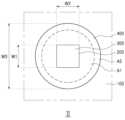
도 1은 본 발명의 일 실시예에 의한 광원 모듈의 평면도이다.
도 2는 도 1의 I-I'축을 따라 절개한 단면도이다.
도 3은 도 2의 'A'부분의 확대도이다.
도 4는 도 3의 'B'부분의 확대도이다.
도 5는 도 3의 II 방향에서 본 평면도이다.
도 6은 도 3의 발광 다이오드 칩 및 다층 반사구조의 확대도이다.
도 7은 도 2의 변형예이다.
도 8, 도 9, 도 10 및 도 12는 광원 모듈의 다양한 실시예이다.
도 11은 도 10의 III-III'축을 따라 절개한 단면도이다.
도 13은 본 발명의 일 실시예에 의한 백 라이트 유닛의 단면도이다.
도 14 및 도 15는 본 발명의 일 실시예에 의한 광원 모듈의 제조공정을 도시한 개략적인 단면도이다.
도 16은 본 발명의 일 실시예에 의한 광원 모듈의 제조공정을 도시한 개략적인 단면도이다.Figure 1 is a plan view of a light source module according to one embodiment of the present invention.
Figure 2 is a cross-sectional view taken along the I-I' axis of Figure 1.
Figure 3 is an enlarged view of part 'A' of Figure 2.
Figure 4 is an enlarged view of part 'B' of Figure 3.
Figure 5 is a plan view taken from direction II of Figure 3.
Figure 6 is an enlarged view of the light-emitting diode chip and multilayer reflective structure of Figure 3.
Fig. 7 is a modified example of Fig. 2.
FIGS. 8, 9, 10, and 12 illustrate various embodiments of light source modules.
Fig. 11 is a cross-sectional view taken along the III-III' axis of Fig. 10.
Fig. 13 is a cross-sectional view of a backlight unit according to one embodiment of the present invention.
FIG. 14 and FIG. 15 are schematic cross-sectional views illustrating a manufacturing process of a light source module according to one embodiment of the present invention.
Fig. 16 is a schematic cross-sectional view illustrating a manufacturing process of a light source module according to one embodiment of the present invention.
이하, 첨부된 도면을 참조하여 본 발명의 실시예들을 다음과 같이 설명한다.Hereinafter, embodiments of the present invention will be described with reference to the attached drawings.
도 1은 본 발명의 일 실시예에 의한 광원 모듈의 평면도이고, 도 2는 도 1의 I-I'축을 따라 절개한 단면도이다. 도 3은 도 2의 'A'부분의 확대도이다.FIG. 1 is a plan view of a light source module according to one embodiment of the present invention, and FIG. 2 is a cross-sectional view taken along the I-I' axis of FIG. 1. FIG. 3 is an enlarged view of portion 'A' of FIG. 2.
도 1 및 도 2를 참조하면, 본 발명의 일 실시예에 의한 광원 모듈(10)은 회로 기판(100) 상에 복수의 발광 다이오드 칩(200)이 소정의 피치(pitch)(PT)로 배열될 수 있다. 일 실시예의 경우, 피치(PT)는 7.5㎜이하 일 수 있다. 각각의 발광 다이오드 칩(200)에는 다층 반사구조(300)가 배치될 수 있으며, 발광 다이오드 칩(200) 및 다층 반사구조(300)를 덮도록 렌즈부(400)가 배치될 수 있다. 일 실시예의 경우, 복수의 발광 다이오드 칩(200)이 회로 기판(100) 상에 매트릭스(matrix) 배열된 것으로 도시되어 있으나, 이에 한정하는 것은 아니며, 헥사고날(hexagonal) 배열과 같은 다양한 구조로 배열될 수 있다.Referring to FIGS. 1 and 2, a light source module (10) according to one embodiment of the present invention may have a plurality of light emitting diode chips (200) arranged at a predetermined pitch (PT) on a circuit board (100). In one embodiment, the pitch (PT) may be 7.5 mm or less. A multilayer reflective structure (300) may be arranged on each light emitting diode chip (200), and a lens unit (400) may be arranged to cover the light emitting diode chip (200) and the multilayer reflective structure (300). In one embodiment, a plurality of light emitting diode chips (200) are illustrated as being arranged in a matrix on a circuit board (100), but this is not limited thereto, and may be arranged in various structures such as a hexagonal arrangement.
회로 기판(100)은 글래스(glass) 기판일 수 있다. 글래스 기판은 유리, 경질 유리, 석영 유리 등으로 이루어진 베이스부에 전극 패턴이 형성된 인쇄회로기판(printed circuit board)일 수 있다. 이러한 글라스 기판은, 유리섬유를 수지에 함침하여 형성한 FR-4를 이용한 인쇄회로기판에 비해 높은 방열 효과를 가지며, 상대적으로 낮은 열 팽창 계수(coefficient of thermal expansion; CTE)를 가진다. 따라서, FR-4를 이용한 기존의 인쇄회로기판에 비해 더욱 미세화된 전극 패턴을 구현할 수 있다.The circuit board (100) may be a glass substrate. The glass substrate may be a printed circuit board having an electrode pattern formed on a base portion made of glass, hard glass, quartz glass, or the like. Such a glass substrate has a high heat dissipation effect and a relatively low coefficient of thermal expansion (CTE) compared to a printed circuit board using FR-4 formed by impregnating glass fibers into a resin. Accordingly, a more refined electrode pattern can be implemented compared to a conventional printed circuit board using FR-4.
도 3 및 도 6을 참조하면, 회로 기판(100)은 베이스부(130) 및 베이스부(130)의 상면에 형성된 제1 및 제2 전극 패턴(110a, 110b)을 포함할 수 있다. 회로 기판(100)의 표면에는, 회로 기판(100)을 전체적으로 덮는 피복층(120)이 배치될 수 있으며, 피복층(120)은 PSR(photo solder resist) 잉크를 도포하여 형성할 수 있다. 제1 및 제2 전극 패턴(110a, 110b)의 일부 영역은 피복층(120)을 관통하여 회로 기판(100)의 표면에 노출되도록 배치되어, 복수의 발광 다이오드 칩(200)과 솔더 범프(solder bump) 등과 같은 전도성 접착층에 의해 전기적으로 연결될 수 있다.Referring to FIGS. 3 and 6, the circuit board (100) may include a base portion (130) and first and second electrode patterns (110a, 110b) formed on an upper surface of the base portion (130). A covering layer (120) that entirely covers the circuit board (100) may be disposed on a surface of the circuit board (100), and the covering layer (120) may be formed by applying PSR (photo solder resist) ink. Some areas of the first and second electrode patterns (110a, 110b) may be disposed to penetrate the covering layer (120) and be exposed to the surface of the circuit board (100), so as to be electrically connected to a plurality of light-emitting diode chips (200) by a conductive adhesive layer such as a solder bump.
복수의 발광 다이오드 칩(200)은 각각 회로 기판(100)의 표면에 실장될 수 있다. 각각의 발광 다이오드 칩(200)은 성장용 기판((210), 발광 구조물(220) 및 제1 및 제2 전극(230a, 230b)을 가질 수 있다.A plurality of light emitting diode chips (200) may be mounted on the surface of a circuit board (100), respectively. Each light emitting diode chip (200) may have a growth substrate (210), a light emitting structure (220), and first and second electrodes (230a, 230b).
복수의 발광 다이오드 칩(200) 각각은 100㎛ 이하의 두께(T1)를 가질 수 있다(도 3 참조). 또한, 도 5를 참조하면, 복수의 발광 다이오드 칩(200)은 각각 상부에서 보았을 때에, 정사각형 또는 직사각형의 형상을 가질 있으며, 정사각형 또는 직사각형의 각 변을 이루는 모서리(W1, W2)는 500㎛ 이하의 크기를 가질 수 있다. 예를 들어, 발광 다이오드 칩(200)은 500㎛×500㎛, 200㎛×300㎛ 및 175㎛×300㎛와 같이 다양한 크기를 가질 수 있다.Each of the plurality of light-emitting diode chips (200) may have a thickness (T1) of 100 μm or less (see FIG. 3). In addition, referring to FIG. 5, each of the plurality of light-emitting diode chips (200) may have a square or rectangular shape when viewed from above, and corners (W1, W2) forming each side of the square or rectangle may have a size of 500 μm or less. For example, the light-emitting diode chips (200) may have various sizes, such as 500 μm×500 μm, 200 μm×300 μm, and 175 μm×300 μm.
도 6을 참조하면, 각각의 발광 다이오드 칩(200)은 제1 면(S1) 및 이에 대향하는 제2 면(S2)을 가질 수 있다. 제1 면(S1)은 후술하는 제2 도전형 반도체층(223)에 의해 제공될 수 있으며, 제2 면(S2)은 후술하는 성장용 기판(210)에 의해 제공될 수 있다. 제1 면(S1)에는 전극(230)이 배치될 수 있으며, 제2 면(S2)에는 다층 반사구조(300)가 적층될 수 있다.Referring to FIG. 6, each light emitting diode chip (200) may have a first surface (S1) and a second surface (S2) opposite thereto. The first surface (S1) may be provided by a second conductive semiconductor layer (223) described later, and the second surface (S2) may be provided by a growth substrate (210) described later. An electrode (230) may be arranged on the first surface (S1), and a multilayer reflective structure (300) may be laminated on the second surface (S2).
성장용 기판(210)은 사파이어, Si, SiC, MgAl2O4, MgO, LiAlO2, LiGaO2, GaN, AlN, 금속기판 등과 같이 절연성, 도전성, 반도체 물질을 이용할 수 있다. 질화물 반도체 성장용 기판으로 널리 이용되는 사파이어는, 전기 절연성을 가지며 육각-롬보형(Hexa-Rhombo R3c) 대칭성을 갖는 결정체로서 c축 및 a측 방향의 격자상수가 각각 13.001Å과 4.758Å이며, C(0001)면, A(11-20)면, R(1-102)면 등을 갖는다. 이 경우, 상기 C면은 비교적 질화물 박막의 성장이 용이하며, 고온에서 안정하기 때문에 질화물 성장용 기판으로 주로 사용된다.The growth substrate (210) can use insulating, conductive, and semiconductor materials such as sapphire, Si, SiC, MgAl2 O4 , MgO, LiAlO2 , LiGaO2 , GaN, AlN, and a metal substrate. Sapphire, which is widely used as a substrate for nitride semiconductor growth, is a crystal that has electrical insulation and a hexagonal-Rhombo R3c symmetry, and the lattice constants in the c-axis and a-direction are 13.001 Å and 4.758 Å, respectively, and has a C (0001) plane, an A (11-20) plane, an R (1-102) plane, etc. In this case, the C plane is mainly used as a substrate for nitride growth because it is relatively easy to grow a nitride thin film on it and it is stable at high temperatures.
발광 구조물(220)은 성장용 기판(210) 상에 순차적으로 배치된 제1 도전형 반도체층(221), 활성층(222) 및 제2 도전형 반도체층(223)을 포함할 수 있다. 제1 및 제2 도전형 반도체층(221, 223)은 각각 n형 및 p형 반도체층이 될 수 있으며, 질화물 반도체로 이루어질 수 있다. 따라서, 이에 제한되는 것은 아니지만, 일 실시예의 경우, 제1 및 제2 도전형 반도체층(221, 223)은 각각 n형 및 p형 반도체층을 의미하는 것으로 이해될 수 있다. 제1 및 제2 도전형 반도체층(221, 223)은 AlxInyGa(1-x-y)N 조성식(여기서, 0≤x<1, 0≤y<1, 0≤x+y<1임)을 가지며, 예컨대 GaN, AlGaN, InGaN 등의 물질로 이루어질 수 있다.The light-emitting structure (220) may include a first conductive semiconductor layer (221), an active layer (222), and a second conductive semiconductor layer (223) sequentially arranged on a growth substrate (210). The first and second conductive semiconductor layers (221, 223) may be n-type and p-type semiconductor layers, respectively, and may be made of nitride semiconductors. Accordingly, although not limited thereto, in one embodiment, the first and second conductive semiconductor layers (221, 223) may be understood to mean n-type and p-type semiconductor layers, respectively. The first and second conductive semiconductor layers (221, 223) have a composition formula of Alx Iny Ga(1-xy) N (wherein, 0≤x<1, 0≤x+y<1) and may be made of a material such as GaN, AlGaN, or InGaN.
활성층(222)은 가시광(약 350∼680㎚ 파장범위)을 발광하기 위한 층일 수 있으며, 단일 또는 다중 양자 우물(multiple quantum well)구조를 갖는 언도프된 질화물 반도체층으로 구성될 수 있다. 일 실시예의 경우, 활성층(222)은 청색광을 방출할 수 있다. 활성층(222)은 예를 들어 AlxInyGa(1-x-y)N (0≤x<1, 0≤y<1, 0≤x+y<1)의 양자장벽층과 양자우물층이 교대로 적층된 다중양자우물구조로 형성되어 소정의 밴드갭을 가지는 구조를 사용할 수 있다. 이와 같은 양자우물구조에 의해 전자 및 정공이 재결합되어 발광한다. 다중 양자우물 구조의 경우, 예컨대, InGaN/GaN 구조가 사용될 수 있다. 제1 및 제2 도전형 반도체층(221, 223)과 활성층(222)은 MOCVD(metalorganic chemical vapor deposition), MBE(molecular beam epitaxy), HVPE(hydride vapour phase epitaxy) 등과 같은 결정 성장 공정을 이용하여 형성될 수 있을 것이다.The active layer (222) may be a layer for emitting visible light (wavelength range of about 350 to 680 nm) and may be composed of an undoped nitride semiconductor layer having a single or multiple quantum well structure. In one embodiment, the active layer (222) may emit blue light. The active layer (222) may use a structure having a predetermined band gap formed by a multiple quantum well structure in which quantum barrier layers and quantum well layers of, for example, Alx Iny Ga(1-xy) N (0≤x<1, 0≤y<1, 0≤x+y<1) are alternately laminated. Electrons and holes are recombined by this quantum well structure to emit light. In the case of the multiple quantum well structure, for example, an InGaN/GaN structure may be used. The first and second challenge type semiconductor layers (221, 223) and the active layer (222) may be formed using a crystal growth process such as MOCVD (metalorganic chemical vapor deposition), MBE (molecular beam epitaxy), HVPE (hydride vapour phase epitaxy), etc.
발광 다이오드 칩(200)은 전극(230)이 일면에만 배치되는, 소위 플립 칩(flip-chip)구조의 발광 다이오드 칩이 사용될 수 있다. 일 실시예의 경우,The light-emitting diode chip (200) may be a light-emitting diode chip of a so-called flip-chip structure in which the electrode (230) is placed on only one side. In one embodiment,
전극(230)은 제1 및 제2 전극(230a, 230b)을 포함할 수 있으며, 제1 및 제2 전극(230a, 230b)은 발광 다이오드 칩(200)의 제2 면(S1)에 배치될 수 있다. 제1 및 제2 전극(230a, 230b)은 각각 제1 및 제2 도전형 반도체층(221, 223)에 외부 전원을 인가하기 위한 것으로, 제1 및 제2 도전형 반도체층(221, 223)과 각각 오믹 접속을 하도록 구비될 수 있다.The electrode (230) may include first and second electrodes (230a, 230b), and the first and second electrodes (230a, 230b) may be arranged on the second surface (S1) of the light-emitting diode chip (200). The first and second electrodes (230a, 230b) are provided to apply external power to the first and second conductive semiconductor layers (221, 223), respectively, and may be provided to form an ohmic connection with the first and second conductive semiconductor layers (221, 223), respectively.
제1 및 제2 전극(230a, 230b)은 각각 제1 및 제2 도전형 반도체층(221, 223)과 오믹 접속의 특성을 갖는 도전성 물질이 1층 또는 다층 구조로 이루어질 수 있으며, 예컨대, Au, Ag, Cu, Zn, Al, In, Ti, Si, Ge, Sn, Mg, Ta, Cr, W, Ru, Rh, Ir, Ni, Pd, Pt, 및 투명 도전성 산화물(TCO) 등의 물질 중 하나 이상을 증착시키거나 스퍼터링하는 공정으로 형성될 수 있다.The first and second electrodes (230a, 230b) may be formed of a single-layer or multi-layer structure of a conductive material having the characteristics of an ohmic connection with the first and second conductive semiconductor layers (221, 223), respectively, and may be formed by a process of depositing or sputtering one or more of materials such as, for example, Au, Ag, Cu, Zn, Al, In, Ti, Si, Ge, Sn, Mg, Ta, Cr, W, Ru, Rh, Ir, Ni, Pd, Pt, and transparent conductive oxide (TCO).
도 6을 참조하면, 발광 다이오드 칩(200)의 제2 면(S2)에는 다층 반사구조(300)가 배치될 수 있다. 다층 반사구조(300)는 발광 구조물(220)을 전체적으로 덮도록 배치될 수 있다. 다층 반사구조(300)는 활성층(222)에서 방출된 광(L) 중 성장용 기판(210)이 배치된 상부 방향으로 향하는 제1 광(L1)을 반사시켜, 발광 다이오드 칩(200)의 측면 방향으로 향하도록 리디렉션(redirection)할 수 있다. 따라서 발광 다이오드 칩(200)의 측면으로 방출되는 광의 양이 증가하며 광 지향각이 전체적으로 증가할 수 있다. 또한, 다층 반사구조(300)는 상부 방향으로 향하는 광(L)의 제2 광(L2)을 투과시켜, 발광 다이오드 칩(200)의 전방으로 제2 광(L2)이 방출되도록 할 수 있다. 따라서, 발광 다이오드 칩(200)의 전방이 상대적으로 어둡게 보이는 이른바 암점의 발생을 방지할 수 있다. 실시예에 따라서는, 도 7에 도시된 바와 같이, 발광 다이오드 칩(200)의 상면과 하면에 각각 다층 반사구조(1300)가 배치될 수도 있다. 즉, 발광 다이오드 칩(200)의 상면에는 제1 다층 반사구조(1310)가 배치되고, 하면에는 제2 다층 반사구조(1320)가 배치될 수 있다.Referring to FIG. 6, a multilayer reflective structure (300) may be arranged on the second surface (S2) of the light emitting diode chip (200). The multilayer reflective structure (300) may be arranged to entirely cover the light emitting structure (220). The multilayer reflective structure (300) may reflect the first light (L1) of the light (L) emitted from the active layer (222) toward an upper direction where the growth substrate (210) is arranged, and redirect the light toward a side direction of the light emitting diode chip (200). Accordingly, the amount of light emitted toward the side of the light emitting diode chip (200) may increase, and the light directivity angle may increase overall. In addition, the multilayer reflective structure (300) may transmit the second light (L2) of the light (L) directed upward, so that the second light (L2) may be emitted toward the front of the light emitting diode chip (200). Accordingly, it is possible to prevent the occurrence of so-called dark spots in which the front of the light-emitting diode chip (200) appears relatively dark. Depending on the embodiment, as shown in FIG. 7, a multilayer reflective structure (1300) may be arranged on the upper and lower surfaces of the light-emitting diode chip (200), respectively. That is, a first multilayer reflective structure (1310) may be arranged on the upper surface of the light-emitting diode chip (200), and a second multilayer reflective structure (1320) may be arranged on the lower surface.
도 6을 참조하면, 다층 반사구조(300)는 굴절률이 서로 다른 층들이 상하방향으로 교대로 적층된 구조로 제공될 수 있다. 구체적으로, 다층 반사구조(300)는 서로 다른 굴절률을 갖는 제1 절연층(300a) 및 제2 절연층(300b)이 교대로 적층된 구조로 배치될 수 있다. 이러한 다층 반사구조(300)는 제1 절연층(300a) 및 제2 절연층(300b)의 굴절률과 두께를 적절히 조절하여, 분산형 브래그 반사기(distributed bragg reflector; DBR)로 제공될 수 있다. 예를 들어, 활성층(222)에서 생성되는 광(L)의 파장을 λ이라고 하고 n을 해당 층의 굴절률이라 할 때에, 다층 반사구조(300)의 제1 절연층(300a) 및 제2 절연층(300b)은 λ/4n의 두께를 갖도록 형성될 수 있으며, 대략 약 300Å 내지 900Å의 두께를 가질 수 있다. 이때, 다층 반사구조(300)는 활성층(222)에서 생성된 광(L)의 파장에 대해서 높은 반사율(90% 이상)을 갖도록 각 제1 절연층(300a) 및 제2 절연층(300b)의 굴절률과 두께가 선택되어 설계될 수 있다. 제1 절연층(300a)과 제2 절연층(300b)은 동일한 두께로 형성될 수 있으나, 서로 다른 두께를 가질 수 있다.Referring to FIG. 6, the multilayer reflective structure (300) may be provided as a structure in which layers having different refractive indices are alternately laminated in the vertical direction. Specifically, the multilayer reflective structure (300) may be arranged as a structure in which first insulating layers (300a) and second insulating layers (300b) having different refractive indices are alternately laminated. This multilayer reflective structure (300) may be provided as a distributed bragg reflector (DBR) by appropriately adjusting the refractive indices and thicknesses of the first insulating layer (300a) and the second insulating layer (300b). For example, when the wavelength of light (L) generated in the active layer (222) is λ and n is the refractive index of the corresponding layer, the first insulating layer (300a) and the second insulating layer (300b) of the multilayer reflective structure (300) can be formed to have a thickness of λ/4n and can have a thickness of approximately 300Å to 900Å. At this time, the multilayer reflective structure (300) can be designed so that the refractive index and thickness of each of the first insulating layer (300a) and the second insulating layer (300b) are selected so as to have a high reflectivity (90% or more) for the wavelength of light (L) generated in the active layer (222). The first insulating layer (300a) and the second insulating layer (300b) can be formed to have the same thickness, but can have different thicknesses.
다층 반사구조(300)를 이루는 제1 절연층(300a)과 제2 절연층(300b)은 절연 특성 및 광투과 특성을 지닌 재료로 이루어질 수 있다. 예를 들어, 다층 반사구조(300)는 실리콘 산화물 또는 실리콘 질화물을 포함하여 이루어질 수 있으며, 구체적으로, SiO2, SiN, SiOxNy, TiO2, Si3N4, Al2O3, TiN, AlN, ZrO2, TiAlN, TiSiN 등으로 이루어질 수 있다. 일 실시예의 경우, 제1 절연층(300a)은 SiO2로 이루어지고, 제2 절연층(300b)은 TiO2로 이루어 질 수 있다.The first insulating layer (300a) and the second insulating layer (300b) forming the multilayer reflective structure (300) may be formed of a material having insulating properties and light transmitting properties. For example, the multilayer reflective structure (300) may be formed of silicon oxide or silicon nitride, and specifically, may be formed of SiO2 , SiN, SiOx Ny , TiO2 , Si3 N4 , Al2 O3 , TiN, AlN, ZrO2 , TiAlN, TiSiN, etc. In one embodiment, the first insulating layer (300a) may be formed of SiO2 , and the second insulating layer (300b) may be formed of TiO2 .
제1 절연층(300a)과 제2 절연층(300b)이 각각 1회 적층된 것을 하나의 절연층 쌍(pair)으로 정의하였을 때, 다층 반사구조(300)는 절연층 쌍이 상하 방향으로 5~30회 반복되어 적층된 구조를 가질 수 있다. 다층 반사구조(300)가 5회 미만의 절연층 쌍을 포함하는 경우에는, 반사도가 낮아 다층 반사구조(300)가 분산형 브래그 반사기로서 동작하기 어렵다. 반면에, 다층 반사구조(300)가 30회를 초과하는 절연층 쌍을 포함하는 경우에는, 다층 반사구조(300)를 투과하는 제2 광(L2)의 양이 급격하게 감소하여 암점이 발생할 수 있다.When the first insulating layer (300a) and the second insulating layer (300b) are each laminated once, it is defined as one insulating layer pair, and the multilayer reflective structure (300) may have a structure in which the insulating layer pairs are laminated 5 to 30 times in the vertical direction. When the multilayer reflective structure (300) includes less than 5 insulating layer pairs, the reflectivity is low, making it difficult for the multilayer reflective structure (300) to operate as a distributed Bragg reflector. On the other hand, when the multilayer reflective structure (300) includes more than 30 insulating layer pairs, the amount of second light (L2) transmitting through the multilayer reflective structure (300) may rapidly decrease, causing dark spots to occur.
도 3 내지 도 5를 참조하여, 렌즈부(400)에 대해 설명한다.Referring to FIGS. 3 to 5, the lens unit (400) will be described.
렌즈부(400)는 회로 기판(100)에 실장된 복수의 발광 다이오드 칩(200)에 각각 대응되는 개수로 구비될 수 있다. 렌즈부(400)는 발광 다이오드 칩(200) 및 다층 반사구조(300)를 덮도록 배치될 수 있다. 렌즈부(400)는 발광 다이오드 칩(200)과 다층 반사구조(300)를 봉지하여 수분 및 열로부터 보호하며, 표면 형상을 조절하여 발광 다이오드 칩(200)에서 방출된 광의 광 지향각을 증가시킬 수 있다.The lens unit (400) may be provided in a number corresponding to each of a plurality of light-emitting diode chips (200) mounted on a circuit board (100). The lens unit (400) may be arranged to cover the light-emitting diode chip (200) and the multilayer reflective structure (300). The lens unit (400) encapsulates the light-emitting diode chip (200) and the multilayer reflective structure (300) to protect them from moisture and heat, and may increase the light beam angle of light emitted from the light-emitting diode chip (200) by controlling the surface shape.
렌즈부(400)는 광투과성 물질로 형성될 수 있으며, 구체적으로, 실리콘, 변형 실리콘, 에폭시, 우레탄, 옥세탄, 아크릴, 폴리카보네이트, 폴리이미드 및 이들의 조합으로 구성된 조성물 등과 같은 투광성을 갖는 절연수지를 발광 다이오드 칩(200)이 실장된 회로 기판(100)에 직접 디스펜싱(dispensing) 공정 또는 드롭렛(droplet) 공정을 통하여 형성할 수 있다.The lens portion (400) may be formed of a light-transmitting material, and specifically, an insulating resin having light-transmitting properties, such as a composition composed of silicone, modified silicone, epoxy, urethane, oxetane, acrylic, polycarbonate, polyimide, and a combination thereof, may be formed through a direct dispensing process or a droplet process on a circuit board (100) on which a light-emitting diode chip (200) is mounted.
도 3을 참조하면, 렌즈부(400)는 0.2~0.4의 종횡비를 가질 수 있다. 종횡비는 회로 기판(100)과 렌즈부(400)가 접하는 영역의 직경(W3)과 렌즈부(400)의 두께(T2)의 비로 정의될 수 있다. 예를 들어, 렌즈부(400)는 1~3㎜의 직경(W3)과 2.5㎜ 이하의 두께(T2)를 가질 수 있다. 따라서, 일 실시예의 렌즈부(400)가 채용된 광원 모듈(10)을 적용한 디스플레이 패널은 매우 얇은 두께를 가질 수 있다.Referring to FIG. 3, the lens unit (400) may have an aspect ratio of 0.2 to 0.4. The aspect ratio may be defined as a ratio of a diameter (W3) of an area where the circuit board (100) and the lens unit (400) come into contact and a thickness (T2) of the lens unit (400). For example, the lens unit (400) may have a diameter (W3) of 1 to 3 mm and a thickness (T2) of 2.5 mm or less. Accordingly, a display panel using a light source module (10) in which the lens unit (400) of one embodiment is employed may have a very thin thickness.
도 3 및 도 4를 참조하면, 렌즈부(400)는 상면에서 보았을 때, 중앙영역에 배치되는 제1 영역(A1)과, 제1 영역(A1)의 둘레에 배치되는 제2 영역(A2)을 가질 수 있다. 제1 영역(A1)은 상부로 볼록한 물방울 형태의 표면 형상을 갖는 영역으로, 높은 종횡비로 인해 발광 다이오드 칩(200)에서 방출된 광의 지향각을 증가시킬 수 있다. 제2 영역(A2)은 외곽으로 갈수록 점점 얇아지며 오목한 표면 형상을 갖는 영역으로, 렌즈부(400)를 형성하는 디스펜싱 공정 또는 드롭렛 공정을 통해 제1 영역(A1)의 둘레에 자연스럽게 형성될 수 있다.Referring to FIGS. 3 and 4, the lens unit (400) may have a first region (A1) disposed in a central region when viewed from the top, and a second region (A2) disposed around the first region (A1). The first region (A1) is a region having a surface shape in the shape of a droplet that is convex upward, and may increase the angle of light emitted from the light emitting diode chip (200) due to a high aspect ratio. The second region (A2) is a region having a surface shape that gradually becomes thinner toward the periphery and becomes concave, and may be naturally formed around the periphery of the first region (A1) through a dispensing process or a droplet process for forming the lens unit (400).
도 4를 참조하면, 제1 영역(A1)과 제2 영역(A2)의 표면 형상은 각각 제1 곡면(C1) 및 제2 곡면(C2)을 갖도록 이루어질 수 있다. 제1 곡면(C1)과 제2 곡면(C2)이 접하는 지점에는 변곡점(P)이 형성될 수 있다. 제2 곡면(C2)은 회로 기판(100)의 상면에 대하여 예각의 접촉각(θ2)을 가질 수 있다. 제1 곡면(C1)의 접선이 회로 기판(100)의 상면과 이루는 각도(θ1)는 접촉각(θ2) 보다 큰 값을 가질 수 있다.Referring to FIG. 4, the surface shapes of the first region (A1) and the second region (A2) may be formed to have a first curved surface (C1) and a second curved surface (C2), respectively. An inflection point (P) may be formed at a point where the first curved surface (C1) and the second curved surface (C2) contact each other. The second curved surface (C2) may have an acute contact angle (θ2) with respect to the upper surface of the circuit board (100). The angle (θ1) formed by the tangent line of the first curved surface (C1) and the upper surface of the circuit board (100) may have a value greater than the contact angle (θ2).
렌즈부(400)의 표면 형상은, 렌즈부(400)를 형성하는 과정에서, 렌즈부(400)를 형성하기 위한 액상의 실리콘 물질의 점도에 따라 조절할 수 있다. 일 실시예의경우, 렌즈부(400)를 이루는 액상의 실리콘은 30,000 내지 100,000cPs의 점도를 가질 수 있다. 30,000 내지 100,000cPs의 점도를 갖는 액상의 실리콘은 액적의 형태로 도팅되면, 특유의 표면 형상을 가지며 경화될 수 있다. 디스펜싱 공정 또는 드롭렛 공정을 통해 형성된 실리콘 물질의 액적(D1)에는, 퍼지려는 힘(F2)과, 응집하려는 힘(F1)이 동시에 작용하여 렌즈부(400)의 표면 형상을 결정하게 된다(도 15 참조). 제1 영역(A1)은 응집하려는 힘(F1)이 퍼지려는 힘(F2)보다 우세하여 상부로 볼록하며 높은 종횡비를 갖는 물방울 형상을 형성하게 된다. 반면에, 제2 영역(A2)은 퍼지려는 힘(F2)이 응집하려는 힘(F1)보다 우세하여, 회로 기판(100)의 표면에 퍼지게 되므로, 낮은 접촉각(θ2)을 갖는 형상으로 형성될 수 있다. 따라서, 제2 영역(A2)은 외곽으로 갈수록 점점 얇게 퍼지는 형상을 가질 수 있다.The surface shape of the lens portion (400) can be adjusted according to the viscosity of the liquid silicone material for forming the lens portion (400) during the process of forming the lens portion (400). In one embodiment, the liquid silicone forming the lens portion (400) can have a viscosity of 30,000 to 100,000 cPs. The liquid silicone having a viscosity of 30,000 to 100,000 cPs can be hardened with a unique surface shape when dotted in the form of a droplet. A force (F2) for spreading and a force (F1) for coagulating are simultaneously applied to the droplet (D1) of the silicone material formed through a dispensing process or a droplet process to determine the surface shape of the lens portion (400) (see FIG. 15). The first region (A1) is formed into a droplet shape that is convex upward and has a high aspect ratio because the cohesive force (F1) is more dominant than the spreading force (F2). On the other hand, the second region (A2) is formed into a shape having a low contact angle (θ2) because the spreading force (F2) is more dominant than the cohesive force (F1), and is spread over the surface of the circuit board (100). Accordingly, the second region (A2) can have a shape that spreads out increasingly thinner toward the outer edge.
도 8 내지 도 12를 참조하여, 광원 모듈의 다양한 실시예에 대해 설명한다.Referring to FIGS. 8 to 12, various embodiments of the light source module are described.
도 8, 도 9, 도 10 및 도 12는 광원 모듈의 다양한 실시예이며, 도 11은 도 10의 III-III'축을 따라 절개한 단면도이다.FIGS. 8, 9, 10, and 12 illustrate various embodiments of a light source module, and FIG. 11 is a cross-sectional view taken along the III-III' axis of FIG. 10.
도 8을 참조하면, 일 실시예는, 렌즈부(2400)가 복수의 층으로 이루어진 경우이다. 렌즈부(2400)를 제외한, 기판(2100), 발광 다이오드 칩(2200) 및 다층 반사구조(2300)의 구성은, 앞서 설명한 실시예와 같으므로, 설명이 중복되는 것을 방지하기 위해 생략한다.Referring to FIG. 8, one embodiment is a case where the lens portion (2400) is composed of multiple layers. The configuration of the substrate (2100), the light-emitting diode chip (2200), and the multilayer reflective structure (2300), excluding the lens portion (2400), is the same as that of the previously described embodiment, and therefore, description is omitted to avoid duplication.
일 실시예의 렌즈부(2400)는 제1 렌즈부(2410)와 제2 렌즈부(2420)가 적층된 구조이다. 제2 렌즈부(2420)는 제1 렌즈부(2410)의 표면을 모두 덮도록 배치될 수 있다. 즉, 제1 렌즈부(2410)는 발광 다이오드 칩(2200)을 각각 덮으며, 기판(2100)의 상면과 접하며, 제2 렌즈부(2420)는 제1 렌즈부(2410)를 덮으며 기판(2100)의 상면과 접하도록 배치될 수 있다. 제1 렌즈부(2410)와 제2 렌즈부(2420)는 서로 다른 점도인 제1 및 제2 점도를 갖는 실리콘 물질로 이루어질 수 있다. 이때, 제1 점도는 제2 점도 보다 큰 값일 수 있다. 또한, 제1 렌즈부(2410)와 제2 렌즈부(2420)는 서로 다른 제1 및 제2 굴절률을 갖는 실리콘 물질로 이루어질 수 있다. 이때, 제1 굴절률은 제2 굴절률 보다 작은 값일 수 있다. 따라서, 제1 렌즈부(2410)와 제2 렌즈부(2420)는 서로 다른 광학적 특성을 가질 수 있다.The lens unit (2400) of one embodiment has a structure in which a first lens unit (2410) and a second lens unit (2420) are laminated. The second lens unit (2420) may be arranged to cover the entire surface of the first lens unit (2410). That is, the first lens unit (2410) may cover each of the light-emitting diode chips (2200) and may be in contact with the upper surface of the substrate (2100), and the second lens unit (2420) may be arranged to cover the first lens unit (2410) and be in contact with the upper surface of the substrate (2100). The first lens unit (2410) and the second lens unit (2420) may be made of a silicone material having first and second viscosities that are different from each other. In this case, the first viscosity may be a value greater than the second viscosity. In addition, the first lens unit (2410) and the second lens unit (2420) may be made of a silicon material having different first and second refractive indices. At this time, the first refractive index may be a value smaller than the second refractive index. Accordingly, the first lens unit (2410) and the second lens unit (2420) may have different optical characteristics.
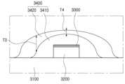
도 9를 참조하면, 일 실시예는, 렌즈부(3400)가 복수의 층으로 이루어진 점에서는 앞서 설명한 실시예와 동일하나, 제2 렌즈부(3420)의 형상이 상이한 경우이다. 제2 렌즈부(3420)를 제외한, 기판(3100), 발광 다이오드 칩(3200), 다층 반사구조(3300) 및 제1 렌즈부(3410)의 구성은, 앞서 설명한 실시예와 같으므로, 설명이 중복되는 것을 방지하기 위해 생략한다.Referring to FIG. 9, one embodiment is the same as the previously described embodiment in that the lens unit (3400) is composed of multiple layers, but the shape of the second lens unit (3420) is different. Except for the second lens unit (3420), the configuration of the substrate (3100), the light-emitting diode chip (3200), the multilayer reflective structure (3300), and the first lens unit (3410) is the same as the previously described embodiment, and therefore, the description is omitted to avoid duplication.
일 실시예의 제2 렌즈부(3420)는 중앙영역에서의 두께(T4)가 가장자리 영역에서의 두께(T3) 보다 얇게 형성된 경우이다. 따라서, 일실시예는 앞서 설명한 실시예와는 다른 광학적 특성을 가질 수 있다.The second lens part (3420) of one embodiment is formed so that the thickness (T4) in the central region is thinner than the thickness (T3) in the edge region. Therefore, one embodiment may have optical characteristics different from those of the previously described embodiment.
도 10 및 도 11을 참조하면, 일 실시예는 렌즈부(4400)가 복수의 층으로 이루어진 점에서는 앞서 설명한 실시예와 동일하나, 제2 렌즈(4420)의 형상이 상이한 경우이다. 제2 렌즈부(4420)를 제외한, 기판(4100), 발광 다이오드 칩(4200), 다층 반사구조(4300) 및 제1 렌즈부(4410)의 구성은, 앞서 설명한 실시예와 같으므로, 설명이 중복되는 것을 방지하기 위해 생략한다.Referring to FIGS. 10 and 11, one embodiment is the same as the previously described embodiment in that the lens portion (4400) is composed of multiple layers, but the shape of the second lens (4420) is different. Except for the second lens portion (4420), the configuration of the substrate (4100), the light-emitting diode chip (4200), the multilayer reflective structure (4300), and the first lens portion (4410) is the same as the previously described embodiment, and therefore, the description is omitted to avoid duplication.
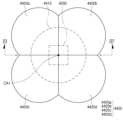
제2 렌즈부(4420)는 상부에서 보았을 때, 제1 렌즈부(4410)의 중심축(CA1)에 대해 일정한 각도마다 회전 대칭된 경우이다. 일 실시예의 경우, 제2 렌즈부(4420)는 90도 마다 회전 대칭되는 형상을 가질 수 있다. 따라서, 4개의 볼록한 영역(4420a~4420d)을 가질 수 있다.The second lens unit (4420) is rotationally symmetrical at a certain angle with respect to the central axis (CA1) of the first lens unit (4410) when viewed from above. In one embodiment, the second lens unit (4420) may have a shape that is rotationally symmetrical at 90 degrees. Accordingly, it may have four convex regions (4420a to 4420d).
도 12는 제2 렌즈부(5420)가 90도 마다 회전 대칭되는 형상인 점에서는 앞서 설명한 실시예와 유사하나, 제2 렌즈부(5420)는 이루는 4개의 볼록한 영역(5420a~5420d)이 중심축(CA2)을 기준으로 θ3만큼 회전 된 경우이다. 제2 렌즈부(5420)를 제외한, 발광 다이오드 칩(5200) 및 제1 렌즈부(5410)의 구성은, 앞서 설명한 실시예와 같으므로, 설명이 중복되는 것을 방지하기 위해 생략한다.FIG. 12 is similar to the previously described embodiment in that the second lens unit (5420) has a shape that is rotationally symmetrical at 90 degrees, but the second lens unit (5420) is a case in which the four convex regions (5420a to 5420d) that it forms are rotated by θ3 around the central axis (CA2). Except for the second lens unit (5420), the configuration of the light-emitting diode chip (5200) and the first lens unit (5410) is the same as the previously described embodiment, and therefore, the description is omitted to avoid duplication.
도 13을 참조하여, 일 실시예에 의한 광학모듈을 이용한 디스플레이 패널(1)에 대해 설명한다. 일 실시예의 디스플레이 패널(1)은 앞서 설명한 도 2의 광원 모듈(10)을 채용한 디스플레이 패널(1)이므로, 광원 모듈(10)에 관한 자세한 설명은 생략한다.Referring to Fig. 13, a display panel (1) using an optical module according to one embodiment will be described. Since the display panel (1) according to one embodiment is a display panel (1) that employs the light source module (10) of Fig. 2 described above, a detailed description of the light source module (10) will be omitted.
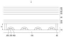
일 실시예의 디스플레이 패널(1)은, 광원 모듈(10), 광학 시트(20), 제1 및 제2 편광판(30, 70), TFT(thin film transistor) 기판(40), TFT 기판(40)과 마주보는 컬러필터 기판(60), TFT 기판(40)과 컬러필터 기판(60) 사이에 마련되는 액정층(50), 및 보호층(80)을 포함할 수 있다. TFT 기판(40)의 하부와 컬러필터 기판(60)의 상부에는 각각 제1 및 제2 편광판(30, 60)이 배치될 수 있으며, 제1 편광판(30)의 하부에는 광학 시트(20) 및 광원 모듈(10)이 배치될 수 있다.A display panel (1) of one embodiment may include a light source module (10), an optical sheet (20), first and second polarizing plates (30, 70), a TFT (thin film transistor) substrate (40), a color filter substrate (60) facing the TFT substrate (40), a liquid crystal layer (50) provided between the TFT substrate (40) and the color filter substrate (60), and a protective layer (80). First and second polarizing plates (30, 60) may be disposed on the lower portion of the TFT substrate (40) and the upper portion of the color filter substrate (60), respectively, and an optical sheet (20) and a light source module (10) may be disposed on the lower portion of the first polarizing plate (30).
광원 모듈(10)의 상부에는 광학 시트(20)가 배치될 수 있다. 일 실시예의 광원 모듈(10)은 청색광을 방출하는 광원일 수 있으며, 광학 시트(20)는 광원 모듈(10)에서 방출된 청색광을 백색광으로 파장변환하여 상부로 방출시킬 수 있다. 광학 시트(20)는 양자점(quantum dot, QD)과 같은 파장변환물질이 액상의 바인더 수지에 분산된 시트일 수 있다. 일 실시예의 경우, 양자점은 청색광을 백색광으로 파장변환할 수 있는 양자점이 포함될 수 있다. 광학 시트(20)는 지지부(90)에 의해 광원 모듈(10)과 소정의 간격(H)을 두고 이격 배치될 수 있다. 일 실시예의 경우, 간격(H)은 3.5㎜ 이하 일 수 있다.An optical sheet (20) may be arranged on the upper portion of the light source module (10). The light source module (10) of one embodiment may be a light source that emits blue light, and the optical sheet (20) may convert the blue light emitted from the light source module (10) into white light and emit it upward. The optical sheet (20) may be a sheet in which a wavelength conversion material, such as a quantum dot (QD), is dispersed in a liquid binder resin. In one embodiment, the quantum dot may include a quantum dot that can convert blue light into white light. The optical sheet (20) may be arranged to be spaced apart from the light source module (10) by a support member (90) at a predetermined distance (H). In one embodiment, the distance (H) may be 3.5 mm or less.
액정층(50)은, 예를 들면, 액정에 가해지는 전기 자극에 따라 광원 모듈(10)로부터 조사되는 광의 투과 양상을 변화시켜 원하는 화상을 표시할 수 있다.The liquid crystal layer (50) can display a desired image by changing the transmission pattern of light irradiated from the light source module (10) according to, for example, an electrical stimulus applied to the liquid crystal.
TFT 기판(40)은, 예를 들면, 복수의 매트릭스 형태로 형성된 게이트 라인 및 복수의 데이터 라인을 포함할 수 있다. 복수의 게이트 라인 및 복수의 데이터 라인의 교차점 각각에는 픽셀 전극 및 박막 트랜지스터가 형성될 수 있다. 박막 트랜지스터를 통해 인가된 신호 전압은 화소 전극에 의해 액정층(50)에 가해지며, 액정층(50)은 신호 전압에 따라 정렬되어 광 투과율을 정할 수 있다.The TFT substrate (40) may include, for example, a plurality of gate lines and a plurality of data lines formed in a matrix form. A pixel electrode and a thin film transistor may be formed at each intersection of the plurality of gate lines and the plurality of data lines. A signal voltage applied through the thin film transistor is applied to the liquid crystal layer (50) by the pixel electrode, and the liquid crystal layer (50) may be aligned according to the signal voltage to determine the light transmittance.
컬러필터 기판(60)은, 예를 들면, 액정층(50)을 사이에 두고 TFT 기판(40)과 대향하는 형태로 배치될 수 있으며, 광이 투과하면서 색이 발현되는 RGB 화소로 이루어진 컬러필터와, 투명 전극(Indium Tin Oxide, ITO)을 포함할 수 있다The color filter substrate (60) may be arranged, for example, in a form facing the TFT substrate (40) with the liquid crystal layer (50) in between, and may include a color filter composed of RGB pixels that express color when light is transmitted, and a transparent electrode (Indium Tin Oxide, ITO).
제2 편광판(70)의 상부에는 보호층(80)이 배치되어, 하부에 배치된 구조물들을 외부의 충격으로부터 보호할 수 있다.A protective layer (80) is placed on the upper part of the second polarizing plate (70) to protect structures placed underneath from external impact.
다음으로, 도 14 내지 도 15를 참조하여, 도 2의 광원 모듈을 제조하는 공정에 대해 설명한다. 도 14 및 도 15는 본 발명의 일 실시예에 의한 광원 모듈의 제조공정을 도시한 개략적인 단면도이다.Next, a process for manufacturing the light source module of Fig. 2 will be described with reference to Figs. 14 and 15. Figs. 14 and 15 are schematic cross-sectional views illustrating a process for manufacturing a light source module according to one embodiment of the present invention.
도 14를 참조하면, 먼저, 회로 기판(100) 상에 복수의 발광 다이오드 칩(200)이 실장될 수 있다. 복수의 발광 다이오드 칩(200)의 상면에는 실장되기 전 다층 반사구조(300)가 형성될 수 있다.Referring to Fig. 14, first, a plurality of light-emitting diode chips (200) may be mounted on a circuit board (100). A multilayer reflective structure (300) may be formed on the upper surface of the plurality of light-emitting diode chips (200) before mounting.
도 15를 참조하면, 복수의 발광 다이오드 칩(200)의 각각에 디스펜싱 공정을 통해 액상의 실리콘 물질의 액적(D1)을 노즐(N1)을 이용하여 도팅함으로써 렌즈부(400)를 형성할 수 있다. 다만, 디스펜싱 공정에 한정하는 것은 아니며 드롭렛과 같은 다양한 방법에 의해서도 형성될 수 있다. 이때, 액상의 실리콘 물질은 30,000 내지 100,000cPs의 점도를 가질 수 있다. 실리콘 물질의 액적(D1)에는, 퍼지려는 힘(F2)과 응집하려는 힘(F1)이 동시에 작용하여 렌즈부(400)의 표면 형상을 결정하게 되는데, 30,000 내지 100,000cPs의 점도를 갖는 실리콘 물질로 형성된 렌즈부(400)의 중앙영역은 응집하려는 힘(F1)이 퍼지려는 힘(F2)보다 우세하여 상부로 볼록하며 높은 종횡비를 갖는 물방울 형상을 형성하며 경화되게 된다. 반면에, 렌즈부(400)의 외곽영역은 퍼지려는 힘(F2)이 응집하려는 힘(F1)보다 우세하여, 회로 기판(100)의 표면에 퍼지게 되므로, 낮은 접촉각을 갖는 형상으로 형성될 수 있다.Referring to FIG. 15, a lens portion (400) may be formed by dotting a liquid silicone material droplet (D1) onto each of a plurality of light-emitting diode chips (200) using a nozzle (N1) through a dispensing process. However, the present invention is not limited to the dispensing process and may also be formed by various methods such as droplets. At this time, the liquid silicone material may have a viscosity of 30,000 to 100,000 cPs. A spreading force (F2) and a cohesive force (F1) simultaneously act on the silicone material droplet (D1) to determine the surface shape of the lens portion (400). In the central region of the lens portion (400) formed of the silicone material having a viscosity of 30,000 to 100,000 cPs, the cohesive force (F1) is more dominant than the spreading force (F2), so that the lens portion is hardened to form a droplet shape that is convex upward and has a high aspect ratio. On the other hand, the outer region of the lens portion (400) has a spreading force (F2) that is stronger than the cohesive force (F1), so it spreads over the surface of the circuit board (100), and can thus be formed into a shape having a low contact angle.
다음으로, 도 16을 참조하여, 도 10의 광원 모듈을 제조하는 공정에 대해 설명한다. 본 발명의 일 실시예에 의한 광원 모듈의 제조공정을 도시한 개략적인 단면도이다. 도 16 이전의 공정은 앞서 설명한 도 15 이후의 공정으로 이해될 수 있다.Next, with reference to FIG. 16, a process for manufacturing the light source module of FIG. 10 will be described. This is a schematic cross-sectional view illustrating a process for manufacturing a light source module according to one embodiment of the present invention. The process before FIG. 16 can be understood as the process after FIG. 15 described above.
도 16을 참조하면, 노즐(N2, N3)을 이용하여 액상의 실리콘 물질의 액적(D2, D3)을 각각의 제1 렌즈부(4410)를 덮도록 도팅함으로써 제2 렌즈부(4420)를 형성할 수 있다. 도 16에는 2개의 노즐(N2, N3)만 도시되어 있으나, 실시예에 따라서는 4개의 노즐이 배치될 수 있다.Referring to FIG. 16, a second lens portion (4420) can be formed by dotting droplets (D2, D3) of a liquid silicone material using nozzles (N2, N3) to cover each first lens portion (4410). Although only two nozzles (N2, N3) are illustrated in FIG. 16, four nozzles may be arranged depending on the embodiment.
본 발명은 상술한 실시형태 및 첨부된 도면에 의해 한정되는 것이 아니며 첨부된 청구범위에 의해 한정하고자 한다. 따라서, 청구범위에 기재된 본 발명의 기술적 사상을 벗어나지 않는 범위 내에서 당 기술분야의 통상의 지식을 가진 자에 의해 다양한 형태의 치환, 변형 및 변경이 가능할 것이며, 이 또한 본 발명의 범위에 속한다고 할 것이다.The present invention is not limited to the above-described embodiments and the attached drawings, but is intended to be limited by the appended claims. Accordingly, various forms of substitution, modification, and change may be made by those skilled in the art within the scope that does not depart from the technical idea of the present invention described in the claims, and this will also fall within the scope of the present invention.
1: 디스플레이 패널
10: 광원 모듈
100: 글래스 기판
200: 발광 다이오드 칩
300: 다층 반사구조
400: 렌즈부1: Display panel
10: Light source module
100: Glass substrate
200: Light-emitting diode chip
300: Multilayer reflective structure
400: Lens section
Claims (20)
Translated fromKorean상기 글래스 기판의 상면에 서로 이격되어 실장되며, 상기 상면을 향하여 배치된 제1 면 및 이에 대향하는 제2 면을 가지며, 상기 제1 면 상에 배치된 제1 및 제2 전극을 가지며, 상기 상면 방향에서 보았을 때 각각의 모서리가 500㎛ 이하의 크기를 가지며 7.5㎜ 이하의 간격으로 이격되어 배치된 복수의 발광 다이오드 칩;
상기 복수의 발광 다이오드 칩의 제2 면을 각각 덮도록 배치되며, 서로 다른 굴절률을 갖는 복수의 절연층들이 교대로 적층된 다층 반사구조; 및
상기 복수의 발광 다이오드 칩을 각각 덮으며, 상기 상면과 접하는 영역의 직경과 높이의 비율이 0.2 내지 0.4이며, 상기 상면과 접하는 접촉각이 예각이며, 30,000 내지 100,000cPs의 점도를 갖는 실리콘 물질을 경화한 제1 렌즈부;를 포함하고,
상기 제1 렌즈부는
중앙에 배치되며 상기 글래스 기판의 상면을 기준으로 볼록하게 돌출된 제1 영역과, 상기 제1 영역의 둘레에 배치되며 상기 글래스 기판의 상면을 기준으로 오목한 제2 영역을 포함하며,
상기 제2 영역은 상기 글래스 기판의 상면과 이루는 접촉각이 예각이고, 상기 제1 렌즈부의 상기 제1 영역 및 상기 제2 영역은 동일한 실리콘 물질로 이루어진 일체화된 구조를 갖는 광원 모듈.
glass substrate;
A plurality of light emitting diode chips mounted on the upper surface of the glass substrate and spaced apart from each other, having a first surface facing the upper surface and a second surface opposing the first surface, and having first and second electrodes arranged on the first surface, each edge having a size of 500 ㎛ or less and spaced apart at intervals of 7.5 mm or less when viewed from the upper surface direction;
A multilayer reflective structure in which a plurality of insulating layers having different refractive indices are alternately laminated, each of which is arranged to cover the second side of the plurality of light-emitting diode chips; and
It includes a first lens part that covers each of the plurality of light-emitting diode chips, has a ratio of a diameter and a height of an area in contact with the upper surface of 0.2 to 0.4, a contact angle in contact with the upper surface is acute, and is made of a hardened silicone material having a viscosity of 30,000 to 100,000 cPs;
The above first lens part
A first region is disposed in the center and protrudes convexly based on the upper surface of the glass substrate, and a second region is disposed around the periphery of the first region and is concave based on the upper surface of the glass substrate.
A light source module in which the second region has an acute contact angle with the upper surface of the glass substrate, and the first region and the second region of the first lens portion have an integrated structure made of the same silicon material.
상기 제1 영역은 볼록하게 돌출된 제1 곡면을 가지며, 상기 제2 영역은 오목한 제2 곡면을 가지고, 상기 접촉각은 상기 제1 곡면의 접선과 상기 글래스 기판의 상면이 이루는 각보다 작은 광원 모듈.
In the first paragraph,
A light source module wherein the first region has a convexly protruding first curved surface, the second region has a concave second curved surface, and the contact angle is smaller than the angle formed by a tangent line of the first curved surface and the upper surface of the glass substrate.
상기 제1 곡면과 상기 제2 곡면이 접하는 영역은 변곡점을 갖는 광원 모듈.
In the second paragraph,
A light source module in which an area where the first surface and the second surface meet has an inflection point.
상기 제1 렌즈부를 덮으며 상기 글래스 기판의 상기 상면과 접하는 영역을 갖는 제2 렌즈부;를 더 포함하는 광원 모듈.
In the first paragraph,
A light source module further comprising a second lens unit covering the first lens unit and having an area in contact with the upper surface of the glass substrate.
상기 제1 렌즈부는 제1 점도를 갖는 실리콘 물질로 이루어지며,
상기 제2 렌즈부는 제2 점도를 갖는 물질로 이루어지며,
상기 제1 점도는 상기 제2 점도 보다 큰 값인 광원 모듈.
In paragraph 4,
The above first lens portion is made of a silicone material having a first viscosity,
The second lens portion is made of a material having a second viscosity,
A light source module wherein the first viscosity has a value greater than the second viscosity.
상기 제2 렌즈부는,
상기 글래스 기판의 상기 상면 방향에서 보았을 때, 상기 제1 렌즈부의 중심축에 대하여 90도 마다 회전 대칭되는 형상을 갖는 광원 모듈.
In paragraph 4,
The above second lens part,
A light source module having a shape that is rotationally symmetrical at 90 degrees with respect to the central axis of the first lens portion when viewed from the upper surface direction of the glass substrate.
상기 제1 렌즈부는 제1 굴절률을 갖는 실리콘 물질로 이루어지며,
상기 제2 렌즈부는 제2 굴절률을 갖는 실리콘 물질로 이루어지며,
상기 제1 굴절률은 상기 제2 굴절률보다 작은 굴절률 값을 갖는 광원 모듈.
In paragraph 4,
The above first lens part is made of a silicone material having a first refractive index,
The second lens portion is made of a silicon material having a second refractive index,
A light source module wherein the first refractive index has a refractive index value smaller than the second refractive index.
상기 제1 렌즈부는 상기 상면을 기준으로 2.5㎜ 이하의 두께를 갖는 광원 모듈.
In the first paragraph,
A light source module wherein the first lens portion has a thickness of 2.5 mm or less based on the upper surface.
상기 복수의 발광 다이오드 칩은 각각,
상기 발광 다이오드 칩의 상기 제2 면을 이루도록 배치된 성장용 기판; 및
상기 성장용 기판 상에 순차적으로 배치된 제1 도전형 반도체층, 활성층 및 제2 도전형 반도체층을 갖는 발광구조물;을 더 포함하며,
상기 제1 및 제2 전극은 상기 제1 및 제2 도전형 반도체층에 각각 접속된 광원 모듈.
In the first paragraph,
Each of the above multiple light emitting diode chips,
A growth substrate arranged to form the second surface of the light-emitting diode chip; and
It further includes a light-emitting structure having a first conductive semiconductor layer, an active layer, and a second conductive semiconductor layer sequentially arranged on the growth substrate;
The above first and second electrodes are a light source module connected to the first and second conductive semiconductor layers, respectively.
상기 다층 반사구조는 제1 굴절률을 갖는 제1 절연층과 제2 굴절률을 갖는 제2 절연층이 교대로 적층되어 분산 브래그 반사기(distributed bragg reflector)를 이루며,
상기 제1 절연층과 상기 제2 절연층은 5 내지 30회 반복하여 적층된 광원 모듈.
In the first paragraph,
The above multilayer reflective structure is formed by alternately stacking a first insulating layer having a first refractive index and a second insulating layer having a second refractive index to form a distributed Bragg reflector.
A light source module in which the first insulating layer and the second insulating layer are repeatedly laminated 5 to 30 times.
상기 회로 기판의 상면에 서로 이격되어 실장되며 상기 상면을 향하여 배치된 제1 면 및 이에 대향하는 제2 면을 가지며, 상기 제1 면 상에 배치된 제1 및 제2 전극을 갖는 복수의 발광 다이오드 칩 - 상기 복수의 발광 다이오드 칩은 청색광을 방출함 -;
상기 복수의 발광 다이오드 칩의 제2 면을 각각 덮도록 배치되며, 서로 다른 굴절률을 갖는 복수의 절연층들이 교대로 적층된 제1 다층 반사구조; 및
상기 복수의 발광 다이오드 칩을 각각 덮으며, 상기 상면과 접하는 접촉각이 예각이며, 상기 상면과 접하는 영역의 직경은 1 내지 3㎜ 이며, 상기 상면을 기준으로 2.5㎜ 이하의 두께를 갖는 제1 렌즈부;를 포함하고,
상기 제1 렌즈부는
중앙에 배치되며 상기 회로 기판의 상면을 기준으로 볼록하게 돌출된 제1 영역과, 상기 제1 영역의 둘레에 배치되며 상기 회로 기판의 상면을 기준으로 오목한 제2 영역을 포함하며,
상기 제2 영역은 상기 회로 기판의 상면과 이루는 접촉각이 예각이고, 상기 제1 렌즈부의 상기 제1 영역 및 상기 제2 영역은 동일한 실리콘 물질로 이루어진 일체화된 구조를 갖는 광원 모듈.
circuit board;
A plurality of light emitting diode chips mounted on an upper surface of the circuit board and spaced apart from each other and having a first surface facing the upper surface and a second surface opposite thereto, and having first and second electrodes arranged on the first surface, wherein the plurality of light emitting diode chips emit blue light;
A first multilayer reflective structure in which a plurality of insulating layers having different refractive indices are alternately laminated and arranged to cover the second surfaces of the plurality of light-emitting diode chips; and
It includes a first lens part that covers each of the plurality of light-emitting diode chips, has an acute contact angle with the upper surface, has a diameter of 1 to 3 mm in the area in contact with the upper surface, and has a thickness of 2.5 mm or less based on the upper surface;
The above first lens part
A first region is disposed in the center and protrudes convexly based on the upper surface of the circuit board, and a second region is disposed around the periphery of the first region and is concave based on the upper surface of the circuit board.
A light source module in which the second region has an acute contact angle with the upper surface of the circuit board, and the first region and the second region of the first lens portion have an integrated structure made of the same silicon material.
상기 복수의 발광 다이오드 칩은 각각,
상기 제1 면을 덮도록 배치되며, 서로 다른 굴절률을 갖는 복수의 절연층들이 교대로 적층된 제2 다층 반사구조를 더 포함하는 광원 모듈.
In Article 11,
Each of the above multiple light emitting diode chips,
A light source module further comprising a second multilayer reflective structure in which a plurality of insulating layers having different refractive indices are alternately laminated, the second multilayer reflective structure being arranged to cover the first surface.
상기 복수의 발광 다이오드 칩은 상기 상면에서 보았을 때 각각의 모서리가 500㎛ 이하의 크기를 가지며 7.5㎜ 이하의 간격으로 이격되어 배치된 광원 모듈.
In Article 11,
The above plurality of light emitting diode chips are a light source module in which each edge has a size of 500㎛ or less when viewed from the top and is spaced apart at intervals of 7.5mm or less.
상기 제1 영역은 중앙에 배치되며 돔 형상을 가지며,
상기 제2 영역은 상기 제1 영역의 둘레에 연장되며 가장자리로 갈수록 점점 얇아지는 두께를 갖는 광원 모듈.
In Article 11,
The above first region is located in the center and has a dome shape,
A light source module in which the second region extends around the perimeter of the first region and has a thickness that gradually becomes thinner toward the edge.
상기 제1 렌즈부의 적어도 일 영역과 중첩되며 상기 회로 기판의 상기 상면과 접하는 복수의 제2 렌즈부;를 더 포함하는 광원 모듈.
In Article 14,
A light source module further comprising a plurality of second lens sections overlapping at least a portion of the first lens section and in contact with the upper surface of the circuit board.
상기 복수의 발광 다이오드 칩은 상기 회로 기판에 각각 플립칩(flip chip) 방식으로 실장된 광원 모듈.
In Article 11,
The above-mentioned plurality of light-emitting diode chips are light source modules each mounted on the circuit board in a flip chip manner.
상기 회로 기판의 상면에 서로 이격되어 실장되며 상기 상면을 향하여 배치된 제1 면 및 이에 대향하는 제2 면을 가지며, 상기 제1 면 상에 배치된 제1 및 제2 전극을 갖는 복수의 발광 다이오드 칩 - 상기 복수의 발광 다이오드 칩은 청색광을 방출함 -;
상기 복수의 발광 다이오드 칩의 상기 제2 면을 덮도록 배치되며, 서로 다른 굴절률을 갖는 복수의 절연층들이 교대로 적층된 다층 반사구조;
상기 복수의 발광 다이오드 칩을 각각 덮으며, 상기 상면과 접하는 영역의 직경과 높이의 비율이 0.2 내지 0.4인 제1 렌즈부; 및
상기 복수의 발광 다이오드 칩의 전방에 배치되며 상기 청색광을 백색광으로 파장변환하는 양자점을 갖는 광학 시트;를 포함하고,
상기 렌즈부는
중앙에 배치되며 상기 회로 기판의 상면을 기준으로 볼록하게 돌출된 제1 영역과, 상기 제1 영역의 둘레에 배치되며 상기 회로 기판의 상면을 기준으로 오목한 제2 영역을 포함하며,
상기 제2 영역은 상기 회로 기판의 상면과 이루는 접촉각이 예각이고, 상기 렌즈부의 상기 제1 영역 및 상기 제2 영역은 동일한 실리콘 물질로 이루어진 일체화된 구조를 갖는 디스플레이 패널.
circuit board;
A plurality of light emitting diode chips mounted on an upper surface of the circuit board and spaced apart from each other and having a first surface facing the upper surface and a second surface opposite thereto, and having first and second electrodes arranged on the first surface, wherein the plurality of light emitting diode chips emit blue light;
A multilayer reflective structure in which a plurality of insulating layers having different refractive indices are alternately laminated, arranged to cover the second surface of the plurality of light-emitting diode chips;
A first lens unit covering each of the plurality of light-emitting diode chips and having a ratio of a diameter and a height of an area in contact with the upper surface of 0.2 to 0.4; and
An optical sheet having quantum dots arranged in front of the plurality of light-emitting diode chips and converting blue light into white light;
The above lens part
A first region is disposed in the center and protrudes convexly based on the upper surface of the circuit board, and a second region is disposed around the periphery of the first region and is concave based on the upper surface of the circuit board.
A display panel in which the second region has an acute contact angle with the upper surface of the circuit board, and the first region and the second region of the lens portion have an integrated structure made of the same silicon material.
상기 복수의 발광 다이오드 칩은 각각 7.5㎜ 이하의 간격으로 이격되어 배치된 디스플레이 패널.
In Article 17,
A display panel in which the above plurality of light-emitting diode chips are arranged at intervals of 7.5 mm or less.
상기 광학 시트의 저면은 상기 회로 기판의 상기 상면과 3.5㎜ 이하의 간격을 두고 배치된 디스플레이 패널.
In Article 17,
A display panel in which the lower surface of the optical sheet is positioned with a gap of 3.5 mm or less from the upper surface of the circuit board.
상기 렌즈부는,
상기 복수의 발광 다이오드 칩을 각각 덮으며, 상기 상면과 접하는 영역의 직경은 2.5 내지 3㎜ 이며, 상기 상면에 대하여 2.5㎜ 이하의 두께를 갖는 디스플레이 패널.
In Article 17,
The above lens part,
A display panel that covers each of the plurality of light-emitting diode chips, has a diameter of an area in contact with the upper surface of 2.5 to 3 mm, and has a thickness of 2.5 mm or less with respect to the upper surface.
Priority Applications (3)
| Application Number | Priority Date | Filing Date | Title |
|---|---|---|---|
| KR1020200032722AKR102801220B1 (en) | 2020-03-17 | 2020-03-17 | Light source module and display panel using the same |
| US17/060,215US11502229B2 (en) | 2020-03-17 | 2020-10-01 | Light source module and display panel using the same |
| US17/986,009US11757076B2 (en) | 2020-03-17 | 2022-11-14 | Light source module and display panel using the same |
Applications Claiming Priority (1)
| Application Number | Priority Date | Filing Date | Title |
|---|---|---|---|
| KR1020200032722AKR102801220B1 (en) | 2020-03-17 | 2020-03-17 | Light source module and display panel using the same |
Publications (2)
| Publication Number | Publication Date |
|---|---|
| KR20210116828A KR20210116828A (en) | 2021-09-28 |
| KR102801220B1true KR102801220B1 (en) | 2025-04-30 |
Family
ID=77746987
Family Applications (1)
| Application Number | Title | Priority Date | Filing Date |
|---|---|---|---|
| KR1020200032722AActiveKR102801220B1 (en) | 2020-03-17 | 2020-03-17 | Light source module and display panel using the same |
Country Status (2)
| Country | Link |
|---|---|
| US (2) | US11502229B2 (en) |
| KR (1) | KR102801220B1 (en) |
Families Citing this family (8)
| Publication number | Priority date | Publication date | Assignee | Title |
|---|---|---|---|---|
| KR102831200B1 (en)* | 2017-02-02 | 2025-07-10 | 서울반도체 주식회사 | Light emitting diode package |
| WO2021140803A1 (en)* | 2020-01-08 | 2021-07-15 | ソニーグループ株式会社 | Light emitting element |
| KR102801220B1 (en)* | 2020-03-17 | 2025-04-30 | 삼성전자주식회사 | Light source module and display panel using the same |
| CN113826222B (en)* | 2020-11-19 | 2023-06-30 | 厦门三安光电有限公司 | DBR structure, LED chip, semiconductor light-emitting device, manufacturing method and display panel |
| EP4328638A4 (en)* | 2021-10-27 | 2024-11-06 | Samsung Electronics Co., Ltd. | DISPLAY DEVICE AND MANUFACTURING METHOD THEREOF |
| EP4465123A4 (en) | 2022-06-24 | 2025-06-18 | Samsung Electronics Co., Ltd | DISPLAY DEVICE |
| KR20240133341A (en)* | 2023-02-28 | 2024-09-04 | 삼성전자주식회사 | Display apparatus |
| CN119225068B (en)* | 2023-06-29 | 2025-10-03 | 合肥京东方瑞晟科技有限公司 | Light-emitting structure, backlight source, and display device |
Citations (2)
| Publication number | Priority date | Publication date | Assignee | Title |
|---|---|---|---|---|
| JP2015526833A (en)* | 2012-04-30 | 2015-09-10 | トゥビタク | Silicon light source and devices using it |
| US20160290587A1 (en)* | 2015-03-31 | 2016-10-06 | Koito Manufacturing Co., Ltd. | Light source unit, method of manufacturing the same, and vehicle lamp |
Family Cites Families (50)
| Publication number | Priority date | Publication date | Assignee | Title |
|---|---|---|---|---|
| CN1143394C (en) | 1996-08-27 | 2004-03-24 | 精工爱普生株式会社 | Peeling method, thin film device transfer method and thin film device |
| USRE38466E1 (en) | 1996-11-12 | 2004-03-16 | Seiko Epson Corporation | Manufacturing method of active matrix substrate, active matrix substrate and liquid crystal display device |
| FR2769375B1 (en)* | 1997-10-08 | 2001-01-19 | Univ Joseph Fourier | VARIABLE FOCAL LENS |
| US7208725B2 (en) | 1998-11-25 | 2007-04-24 | Rohm And Haas Electronic Materials Llc | Optoelectronic component with encapsulant |
| JP3906654B2 (en) | 2000-07-18 | 2007-04-18 | ソニー株式会社 | Semiconductor light emitting device and semiconductor light emitting device |
| US6818465B2 (en) | 2001-08-22 | 2004-11-16 | Sony Corporation | Nitride semiconductor element and production method for nitride semiconductor element |
| JP2003218034A (en) | 2002-01-17 | 2003-07-31 | Sony Corp | Selective growth method, semiconductor light emitting device and method of manufacturing the same |
| JP3815335B2 (en) | 2002-01-18 | 2006-08-30 | ソニー株式会社 | Semiconductor light emitting device and manufacturing method thereof |
| KR100499129B1 (en) | 2002-09-02 | 2005-07-04 | 삼성전기주식회사 | Light emitting laser diode and fabricatin method thereof |
| US7002182B2 (en) | 2002-09-06 | 2006-02-21 | Sony Corporation | Semiconductor light emitting device integral type semiconductor light emitting unit image display unit and illuminating unit |
| KR100714639B1 (en) | 2003-10-21 | 2007-05-07 | 삼성전기주식회사 | Light emitting element |
| KR100506740B1 (en) | 2003-12-23 | 2005-08-08 | 삼성전기주식회사 | Nitride semiconductor light emitting device and method of manufacturing the same |
| KR100664985B1 (en) | 2004-10-26 | 2007-01-09 | 삼성전기주식회사 | Nitride-based semiconductor device |
| US7777247B2 (en)* | 2005-01-14 | 2010-08-17 | Cree, Inc. | Semiconductor light emitting device mounting substrates including a conductive lead extending therein |
| KR100665222B1 (en) | 2005-07-26 | 2007-01-09 | 삼성전기주식회사 | LED package using diffusion material and manufacturing method thereof |
| KR100661614B1 (en) | 2005-10-07 | 2006-12-26 | 삼성전기주식회사 | Nitride-based semiconductor light emitting device and its manufacturing method |
| US7453629B2 (en)* | 2005-12-29 | 2008-11-18 | Lucent Technologies Inc. | Semiconductor optical amplifier pulse reshaper |
| KR100723247B1 (en) | 2006-01-10 | 2007-05-29 | 삼성전기주식회사 | Chip coated LED package and manufacturing method thereof |
| KR100735325B1 (en) | 2006-04-17 | 2007-07-04 | 삼성전기주식회사 | Light emitting diode package and its manufacturing method |
| US7626210B2 (en) | 2006-06-09 | 2009-12-01 | Philips Lumileds Lighting Company, Llc | Low profile side emitting LED |
| US7470974B2 (en)* | 2006-07-14 | 2008-12-30 | Cabot Corporation | Substantially transparent material for use with light-emitting device |
| KR100930171B1 (en) | 2006-12-05 | 2009-12-07 | 삼성전기주식회사 | White light emitting device and white light source module using same |
| KR100855065B1 (en) | 2007-04-24 | 2008-08-29 | 삼성전기주식회사 | Light emitting diode package |
| KR101289069B1 (en)* | 2007-05-09 | 2013-07-22 | 엘지디스플레이 주식회사 | Light emitting diode package having structure of dual lens and liquid crystal display device thereby |
| KR100982980B1 (en) | 2007-05-15 | 2010-09-17 | 삼성엘이디 주식회사 | Surface light source device and LCD backlight unit having same |
| KR101164026B1 (en) | 2007-07-12 | 2012-07-18 | 삼성전자주식회사 | Nitride semiconductor light emitting device and fabrication method thereof |
| KR100891761B1 (en) | 2007-10-19 | 2009-04-07 | 삼성전기주식회사 | Semiconductor light emitting device, manufacturing method thereof and semiconductor light emitting device package using same |
| KR101332794B1 (en) | 2008-08-05 | 2013-11-25 | 삼성전자주식회사 | Light emitting device, light emitting system comprising the same, and fabricating method of the light emitting device and the light emitting system |
| KR20100030470A (en) | 2008-09-10 | 2010-03-18 | 삼성전자주식회사 | Light emitting device and system providing white light with various color temperatures |
| KR101530876B1 (en) | 2008-09-16 | 2015-06-23 | 삼성전자 주식회사 | Light emitting device with increased light emitting amount, light emitting device including same, method of manufacturing light emitting device and light emitting device |
| US8008683B2 (en) | 2008-10-22 | 2011-08-30 | Samsung Led Co., Ltd. | Semiconductor light emitting device |
| US8368112B2 (en)* | 2009-01-14 | 2013-02-05 | Cree Huizhou Opto Limited | Aligned multiple emitter package |
| US9583678B2 (en)* | 2009-09-18 | 2017-02-28 | Soraa, Inc. | High-performance LED fabrication |
| KR20110061067A (en) | 2009-12-01 | 2011-06-09 | 한국광기술원 | Light emitting diode comprising wavelength converting material and diffusing material, and manufacturing method thereof |
| TWI561770B (en)* | 2010-04-30 | 2016-12-11 | Samsung Electronics Co Ltd | Light emitting device package, light source module, backlight unit, display apparatus, television set, and illumination apparatus |
| US10147853B2 (en) | 2011-03-18 | 2018-12-04 | Cree, Inc. | Encapsulant with index matched thixotropic agent |
| JP6199281B2 (en) | 2012-03-23 | 2017-09-20 | シャープ株式会社 | Semiconductor light emitting device, method for manufacturing semiconductor light emitting device, semiconductor light emitting device, and substrate |
| CN113130725B (en)* | 2015-03-31 | 2024-09-24 | 科锐Led公司 | Light emitting diode with encapsulation and method |
| US10304811B2 (en)* | 2015-09-04 | 2019-05-28 | Hong Kong Beida Jade Bird Display Limited | Light-emitting diode display panel with micro lens array |
| JP6524904B2 (en) | 2015-12-22 | 2019-06-05 | 日亜化学工業株式会社 | Light emitting device |
| JP6365592B2 (en) | 2016-05-31 | 2018-08-01 | 日亜化学工業株式会社 | Light emitting device |
| EP3273297B1 (en)* | 2016-07-20 | 2021-05-26 | Nichia Corporation | Light emitting device |
| JP6857496B2 (en) | 2016-12-26 | 2021-04-14 | 日亜化学工業株式会社 | Light emitting device |
| CN109031773A (en)* | 2017-06-09 | 2018-12-18 | 群创光电股份有限公司 | Display device |
| CN116884966A (en) | 2017-07-21 | 2023-10-13 | 日亚化学工业株式会社 | Backlight device and light source |
| US10797027B2 (en)* | 2017-12-05 | 2020-10-06 | Seoul Semiconductor Co., Ltd. | Displaying apparatus having light emitting device, method of manufacturing the same and method of transferring light emitting device |
| WO2020013460A1 (en)* | 2018-07-12 | 2020-01-16 | 서울반도체주식회사 | Light emitting device, light emitting diode package, backlight unit, and liquid crystal display |
| CN109952641B (en)* | 2019-01-15 | 2023-01-10 | 泉州三安半导体科技有限公司 | Light emitting diode package device and light emitting apparatus |
| US11037912B1 (en)* | 2020-01-31 | 2021-06-15 | X Display Company Technology Limited | LED color displays with multiple LEDs connected in series and parallel in different sub-pixels of a pixel |
| KR102801220B1 (en)* | 2020-03-17 | 2025-04-30 | 삼성전자주식회사 | Light source module and display panel using the same |
- 2020
- 2020-03-17KRKR1020200032722Apatent/KR102801220B1/enactiveActive
- 2020-10-01USUS17/060,215patent/US11502229B2/enactiveActive
- 2022
- 2022-11-14USUS17/986,009patent/US11757076B2/enactiveActive
Patent Citations (2)
| Publication number | Priority date | Publication date | Assignee | Title |
|---|---|---|---|---|
| JP2015526833A (en)* | 2012-04-30 | 2015-09-10 | トゥビタク | Silicon light source and devices using it |
| US20160290587A1 (en)* | 2015-03-31 | 2016-10-06 | Koito Manufacturing Co., Ltd. | Light source unit, method of manufacturing the same, and vehicle lamp |
Also Published As
| Publication number | Publication date |
|---|---|
| US20210296393A1 (en) | 2021-09-23 |
| US20230073808A1 (en) | 2023-03-09 |
| US11757076B2 (en) | 2023-09-12 |
| US11502229B2 (en) | 2022-11-15 |
| KR20210116828A (en) | 2021-09-28 |
Similar Documents
| Publication | Publication Date | Title |
|---|---|---|
| KR102801220B1 (en) | Light source module and display panel using the same | |
| CN214848634U (en) | Light-emitting module and display device | |
| US9224926B2 (en) | Light-emitting device and lighting system | |
| US20120043575A1 (en) | Light emitting diode | |
| CN215869440U (en) | Light emitting element, unit pixel and display device | |
| US20210384388A1 (en) | Unit pixel having light emitting device and displaying apparatus | |
| KR20170026801A (en) | Semiconductor light emitting device package and light source module using the same | |
| CA3169833A1 (en) | Display device, pixel module, and unit pixel having light-emitting diode | |
| US20240413135A1 (en) | Unit pixel having light emitting device, method of fabricating the same, and displaying apparatus having the same | |
| US20250022856A1 (en) | Unit pixel and displaying apparatus including the unit pixel | |
| US12027654B2 (en) | Unit pixel having light emitting device and displaying apparatus | |
| US20240113150A1 (en) | Light emitting device and light emitting module having the same | |
| CN214848667U (en) | Unit pixel and display device | |
| KR20160087048A (en) | Light emitting diode package | |
| KR102127446B1 (en) | Light emitting device package and light emitting device array | |
| US20230369304A1 (en) | Pixel device and display apparatus having the same | |
| US20230352619A1 (en) | Light emitting device and light emitting module having the same | |
| CN215896385U (en) | Wafers for unit pixel fabrication | |
| US20220199857A1 (en) | Unit pixel and displaying apparatus including the unit pixel | |
| US20230034456A1 (en) | Light emitting module and display apparatus by using the same | |
| US20240213415A1 (en) | Light-emitting diode package | |
| KR101983779B1 (en) | A light emitting device package | |
| KR20110127438A (en) | Light emitting device, light emitting device manufacturing method and light emitting device package | |
| KR20230096836A (en) | Light emitting diode |
Legal Events
| Date | Code | Title | Description |
|---|---|---|---|
| PA0109 | Patent application | Patent event code:PA01091R01D Comment text:Patent Application Patent event date:20200317 | |
| PG1501 | Laying open of application | ||
| A201 | Request for examination | ||
| PA0201 | Request for examination | Patent event code:PA02012R01D Patent event date:20230116 Comment text:Request for Examination of Application Patent event code:PA02011R01I Patent event date:20200317 Comment text:Patent Application | |
| E902 | Notification of reason for refusal | ||
| PE0902 | Notice of grounds for rejection | Comment text:Notification of reason for refusal Patent event date:20240620 Patent event code:PE09021S01D | |
| E701 | Decision to grant or registration of patent right | ||
| PE0701 | Decision of registration | Patent event code:PE07011S01D Comment text:Decision to Grant Registration Patent event date:20250227 | |
| GRNT | Written decision to grant | ||
| PR0701 | Registration of establishment | Comment text:Registration of Establishment Patent event date:20250423 Patent event code:PR07011E01D | |
| PR1002 | Payment of registration fee | Payment date:20250424 End annual number:3 Start annual number:1 | |
| PG1601 | Publication of registration |