KR102799625B1 - Display and manufacturing method of the same - Google Patents
Display and manufacturing method of the sameDownload PDFInfo
- Publication number
- KR102799625B1 KR102799625B1KR1020180141306AKR20180141306AKR102799625B1KR 102799625 B1KR102799625 B1KR 102799625B1KR 1020180141306 AKR1020180141306 AKR 1020180141306AKR 20180141306 AKR20180141306 AKR 20180141306AKR 102799625 B1KR102799625 B1KR 102799625B1
- Authority
- KR
- South Korea
- Prior art keywords
- connecting metal
- substrate
- metal material
- delete delete
- forming
- Prior art date
- Legal status (The legal status is an assumption and is not a legal conclusion. Google has not performed a legal analysis and makes no representation as to the accuracy of the status listed.)
- Active
Links
- 238000004519manufacturing processMethods0.000titleclaimsabstractdescription16
- 239000000758substrateSubstances0.000claimsabstractdescription81
- 239000002184metalSubstances0.000claimsabstractdescription45
- 229910052751metalInorganic materials0.000claimsabstractdescription45
- 239000007769metal materialSubstances0.000claimsabstractdescription44
- 239000011521glassSubstances0.000claimsabstractdescription29
- 239000006059cover glassSubstances0.000claimsabstractdescription28
- 239000007787solidSubstances0.000claimsabstractdescription16
- 230000001678irradiating effectEffects0.000claimsabstractdescription3
- 238000003825pressingMethods0.000claimsabstractdescription3
- 238000000034methodMethods0.000claimsdescription27
- RZVAJINKPMORJF-UHFFFAOYSA-NAcetaminophenChemical compoundCC(=O)NC1=CC=C(O)C=C1RZVAJINKPMORJF-UHFFFAOYSA-N0.000claimsdescription4
- 239000005388borosilicate glassSubstances0.000claimsdescription4
- 239000005297pyrexSubstances0.000claimsdescription4
- 239000010453quartzSubstances0.000claimsdescription4
- VYPSYNLAJGMNEJ-UHFFFAOYSA-Nsilicon dioxideInorganic materialsO=[Si]=OVYPSYNLAJGMNEJ-UHFFFAOYSA-N0.000claimsdescription4
- 239000005361soda-lime glassSubstances0.000claimsdescription4
- 238000010030laminatingMethods0.000claims1
- 239000010408filmSubstances0.000description36
- 239000010410layerSubstances0.000description22
- 239000004372Polyvinyl alcoholSubstances0.000description4
- 239000004973liquid crystal related substanceSubstances0.000description4
- 229920002451polyvinyl alcoholPolymers0.000description4
- 230000000149penetrating effectEffects0.000description3
- 229920002284Cellulose triacetatePolymers0.000description2
- NNLVGZFZQQXQNW-ADJNRHBOSA-N[(2r,3r,4s,5r,6s)-4,5-diacetyloxy-3-[(2s,3r,4s,5r,6r)-3,4,5-triacetyloxy-6-(acetyloxymethyl)oxan-2-yl]oxy-6-[(2r,3r,4s,5r,6s)-4,5,6-triacetyloxy-2-(acetyloxymethyl)oxan-3-yl]oxyoxan-2-yl]methyl acetateChemical compoundO([C@@H]1O[C@@H]([C@H]([C@H](OC(C)=O)[C@H]1OC(C)=O)O[C@H]1[C@@H]([C@@H](OC(C)=O)[C@H](OC(C)=O)[C@@H](COC(C)=O)O1)OC(C)=O)COC(=O)C)[C@@H]1[C@@H](COC(C)=O)O[C@@H](OC(C)=O)[C@H](OC(C)=O)[C@H]1OC(C)=ONNLVGZFZQQXQNW-ADJNRHBOSA-N0.000description2
- PNDPGZBMCMUPRI-UHFFFAOYSA-NiodineChemical compoundIIPNDPGZBMCMUPRI-UHFFFAOYSA-N0.000description2
- 230000010287polarizationEffects0.000description2
- 229920001721polyimidePolymers0.000description2
- 239000011241protective layerSubstances0.000description2
- 239000011347resinSubstances0.000description2
- 229920005989resinPolymers0.000description2
- QTBSBXVTEAMEQO-UHFFFAOYSA-MAcetateChemical compoundCC([O-])=OQTBSBXVTEAMEQO-UHFFFAOYSA-M0.000description1
- 239000004925Acrylic resinSubstances0.000description1
- 229920000178Acrylic resinPolymers0.000description1
- 229910020658PbSnInorganic materials0.000description1
- 101150071746Pbsn geneProteins0.000description1
- 239000004642PolyimideSubstances0.000description1
- 239000013078crystalSubstances0.000description1
- 230000007423decreaseEffects0.000description1
- 230000006866deteriorationEffects0.000description1
- 239000012530fluidSubstances0.000description1
- 229910052736halogenInorganic materials0.000description1
- -1halogen saltChemical class0.000description1
- 229910052738indiumInorganic materials0.000description1
- 229910052745leadInorganic materials0.000description1
- 229910001092metal group alloyInorganic materials0.000description1
- 238000012986modificationMethods0.000description1
- 230000004048modificationEffects0.000description1
- 229920000636poly(norbornene) polymerPolymers0.000description1
- 229920001225polyester resinPolymers0.000description1
- 239000004645polyester resinSubstances0.000description1
- 239000009719polyimide resinSubstances0.000description1
- 239000002861polymer materialSubstances0.000description1
- 229920005672polyolefin resinPolymers0.000description1
- 229910000679solderInorganic materials0.000description1
- 238000006467substitution reactionMethods0.000description1
- 239000010409thin filmSubstances0.000description1
- 229910052718tinInorganic materials0.000description1
- 229910052725zincInorganic materials0.000description1
Images


Classifications
- H—ELECTRICITY
- H01—ELECTRIC ELEMENTS
- H01L—SEMICONDUCTOR DEVICES NOT COVERED BY CLASS H10
- H01L21/00—Processes or apparatus adapted for the manufacture or treatment of semiconductor or solid state devices or of parts thereof
- H01L21/70—Manufacture or treatment of devices consisting of a plurality of solid state components formed in or on a common substrate or of parts thereof; Manufacture of integrated circuit devices or of parts thereof
- H01L21/71—Manufacture of specific parts of devices defined in group H01L21/70
- H01L21/768—Applying interconnections to be used for carrying current between separate components within a device comprising conductors and dielectrics
- H01L21/76898—Applying interconnections to be used for carrying current between separate components within a device comprising conductors and dielectrics formed through a semiconductor substrate
- H—ELECTRICITY
- H05—ELECTRIC TECHNIQUES NOT OTHERWISE PROVIDED FOR
- H05K—PRINTED CIRCUITS; CASINGS OR CONSTRUCTIONAL DETAILS OF ELECTRIC APPARATUS; MANUFACTURE OF ASSEMBLAGES OF ELECTRICAL COMPONENTS
- H05K1/00—Printed circuits
- H05K1/02—Details
- H05K1/14—Structural association of two or more printed circuits
- H05K1/147—Structural association of two or more printed circuits at least one of the printed circuits being bent or folded, e.g. by using a flexible printed circuit
- H—ELECTRICITY
- H05—ELECTRIC TECHNIQUES NOT OTHERWISE PROVIDED FOR
- H05K—PRINTED CIRCUITS; CASINGS OR CONSTRUCTIONAL DETAILS OF ELECTRIC APPARATUS; MANUFACTURE OF ASSEMBLAGES OF ELECTRICAL COMPONENTS
- H05K1/00—Printed circuits
- H05K1/02—Details
- H05K1/11—Printed elements for providing electric connections to or between printed circuits
- H05K1/117—Pads along the edge of rigid circuit boards, e.g. for pluggable connectors
- G—PHYSICS
- G02—OPTICS
- G02F—OPTICAL DEVICES OR ARRANGEMENTS FOR THE CONTROL OF LIGHT BY MODIFICATION OF THE OPTICAL PROPERTIES OF THE MEDIA OF THE ELEMENTS INVOLVED THEREIN; NON-LINEAR OPTICS; FREQUENCY-CHANGING OF LIGHT; OPTICAL LOGIC ELEMENTS; OPTICAL ANALOGUE/DIGITAL CONVERTERS
- G02F1/00—Devices or arrangements for the control of the intensity, colour, phase, polarisation or direction of light arriving from an independent light source, e.g. switching, gating or modulating; Non-linear optics
- G02F1/01—Devices or arrangements for the control of the intensity, colour, phase, polarisation or direction of light arriving from an independent light source, e.g. switching, gating or modulating; Non-linear optics for the control of the intensity, phase, polarisation or colour
- G02F1/13—Devices or arrangements for the control of the intensity, colour, phase, polarisation or direction of light arriving from an independent light source, e.g. switching, gating or modulating; Non-linear optics for the control of the intensity, phase, polarisation or colour based on liquid crystals, e.g. single liquid crystal display cells
- G02F1/1303—Apparatus specially adapted to the manufacture of LCDs
- G—PHYSICS
- G02—OPTICS
- G02F—OPTICAL DEVICES OR ARRANGEMENTS FOR THE CONTROL OF LIGHT BY MODIFICATION OF THE OPTICAL PROPERTIES OF THE MEDIA OF THE ELEMENTS INVOLVED THEREIN; NON-LINEAR OPTICS; FREQUENCY-CHANGING OF LIGHT; OPTICAL LOGIC ELEMENTS; OPTICAL ANALOGUE/DIGITAL CONVERTERS
- G02F1/00—Devices or arrangements for the control of the intensity, colour, phase, polarisation or direction of light arriving from an independent light source, e.g. switching, gating or modulating; Non-linear optics
- G02F1/01—Devices or arrangements for the control of the intensity, colour, phase, polarisation or direction of light arriving from an independent light source, e.g. switching, gating or modulating; Non-linear optics for the control of the intensity, phase, polarisation or colour
- G02F1/13—Devices or arrangements for the control of the intensity, colour, phase, polarisation or direction of light arriving from an independent light source, e.g. switching, gating or modulating; Non-linear optics for the control of the intensity, phase, polarisation or colour based on liquid crystals, e.g. single liquid crystal display cells
- G02F1/133—Constructional arrangements; Operation of liquid crystal cells; Circuit arrangements
- G02F1/1333—Constructional arrangements; Manufacturing methods
- G02F1/1345—Conductors connecting electrodes to cell terminals
- H—ELECTRICITY
- H01—ELECTRIC ELEMENTS
- H01L—SEMICONDUCTOR DEVICES NOT COVERED BY CLASS H10
- H01L21/00—Processes or apparatus adapted for the manufacture or treatment of semiconductor or solid state devices or of parts thereof
- H01L21/67—Apparatus specially adapted for handling semiconductor or electric solid state devices during manufacture or treatment thereof; Apparatus specially adapted for handling wafers during manufacture or treatment of semiconductor or electric solid state devices or components ; Apparatus not specifically provided for elsewhere
- H01L21/683—Apparatus specially adapted for handling semiconductor or electric solid state devices during manufacture or treatment thereof; Apparatus specially adapted for handling wafers during manufacture or treatment of semiconductor or electric solid state devices or components ; Apparatus not specifically provided for elsewhere for supporting or gripping
- H01L21/6835—Apparatus specially adapted for handling semiconductor or electric solid state devices during manufacture or treatment thereof; Apparatus specially adapted for handling wafers during manufacture or treatment of semiconductor or electric solid state devices or components ; Apparatus not specifically provided for elsewhere for supporting or gripping using temporarily an auxiliary support
- H01L21/6836—Wafer tapes, e.g. grinding or dicing support tapes
- H—ELECTRICITY
- H01—ELECTRIC ELEMENTS
- H01L—SEMICONDUCTOR DEVICES NOT COVERED BY CLASS H10
- H01L23/00—Details of semiconductor or other solid state devices
- H01L23/48—Arrangements for conducting electric current to or from the solid state body in operation, e.g. leads, terminal arrangements ; Selection of materials therefor
- H01L23/481—Internal lead connections, e.g. via connections, feedthrough structures
- H—ELECTRICITY
- H05—ELECTRIC TECHNIQUES NOT OTHERWISE PROVIDED FOR
- H05K—PRINTED CIRCUITS; CASINGS OR CONSTRUCTIONAL DETAILS OF ELECTRIC APPARATUS; MANUFACTURE OF ASSEMBLAGES OF ELECTRICAL COMPONENTS
- H05K1/00—Printed circuits
- H05K1/02—Details
- H05K1/11—Printed elements for providing electric connections to or between printed circuits
- H05K1/111—Pads for surface mounting, e.g. lay-out
- H05K1/112—Pads for surface mounting, e.g. lay-out directly combined with via connections
- H05K1/113—Via provided in pad; Pad over filled via
- H—ELECTRICITY
- H05—ELECTRIC TECHNIQUES NOT OTHERWISE PROVIDED FOR
- H05K—PRINTED CIRCUITS; CASINGS OR CONSTRUCTIONAL DETAILS OF ELECTRIC APPARATUS; MANUFACTURE OF ASSEMBLAGES OF ELECTRICAL COMPONENTS
- H05K1/00—Printed circuits
- H05K1/18—Printed circuits structurally associated with non-printed electric components
- H05K1/189—Printed circuits structurally associated with non-printed electric components characterised by the use of a flexible or folded printed circuit
- H—ELECTRICITY
- H05—ELECTRIC TECHNIQUES NOT OTHERWISE PROVIDED FOR
- H05K—PRINTED CIRCUITS; CASINGS OR CONSTRUCTIONAL DETAILS OF ELECTRIC APPARATUS; MANUFACTURE OF ASSEMBLAGES OF ELECTRICAL COMPONENTS
- H05K3/00—Apparatus or processes for manufacturing printed circuits
- H05K3/36—Assembling printed circuits with other printed circuits
- H05K3/361—Assembling flexible printed circuits with other printed circuits
- H05K3/363—Assembling flexible printed circuits with other printed circuits by soldering
- H—ELECTRICITY
- H05—ELECTRIC TECHNIQUES NOT OTHERWISE PROVIDED FOR
- H05K—PRINTED CIRCUITS; CASINGS OR CONSTRUCTIONAL DETAILS OF ELECTRIC APPARATUS; MANUFACTURE OF ASSEMBLAGES OF ELECTRICAL COMPONENTS
- H05K3/00—Apparatus or processes for manufacturing printed circuits
- H05K3/40—Forming printed elements for providing electric connections to or between printed circuits
- H05K3/4038—Through-connections; Vertical interconnect access [VIA] connections
- H—ELECTRICITY
- H01—ELECTRIC ELEMENTS
- H01L—SEMICONDUCTOR DEVICES NOT COVERED BY CLASS H10
- H01L2221/00—Processes or apparatus adapted for the manufacture or treatment of semiconductor or solid state devices or of parts thereof covered by H01L21/00
- H01L2221/67—Apparatus for handling semiconductor or electric solid state devices during manufacture or treatment thereof; Apparatus for handling wafers during manufacture or treatment of semiconductor or electric solid state devices or components; Apparatus not specifically provided for elsewhere
- H01L2221/683—Apparatus for handling semiconductor or electric solid state devices during manufacture or treatment thereof; Apparatus for handling wafers during manufacture or treatment of semiconductor or electric solid state devices or components; Apparatus not specifically provided for elsewhere for supporting or gripping
- H01L2221/68304—Apparatus for handling semiconductor or electric solid state devices during manufacture or treatment thereof; Apparatus for handling wafers during manufacture or treatment of semiconductor or electric solid state devices or components; Apparatus not specifically provided for elsewhere for supporting or gripping using temporarily an auxiliary support
- H01L2221/68359—Apparatus for handling semiconductor or electric solid state devices during manufacture or treatment thereof; Apparatus for handling wafers during manufacture or treatment of semiconductor or electric solid state devices or components; Apparatus not specifically provided for elsewhere for supporting or gripping using temporarily an auxiliary support used as a support during manufacture of interconnect decals or build up layers
- H—ELECTRICITY
- H01—ELECTRIC ELEMENTS
- H01L—SEMICONDUCTOR DEVICES NOT COVERED BY CLASS H10
- H01L2224/00—Indexing scheme for arrangements for connecting or disconnecting semiconductor or solid-state bodies and methods related thereto as covered by H01L24/00
- H01L2224/73—Means for bonding being of different types provided for in two or more of groups H01L2224/10, H01L2224/18, H01L2224/26, H01L2224/34, H01L2224/42, H01L2224/50, H01L2224/63, H01L2224/71
- H01L2224/732—Location after the connecting process
- H01L2224/73201—Location after the connecting process on the same surface
- H01L2224/73203—Bump and layer connectors
- H01L2224/73204—Bump and layer connectors the bump connector being embedded into the layer connector
- H—ELECTRICITY
- H05—ELECTRIC TECHNIQUES NOT OTHERWISE PROVIDED FOR
- H05K—PRINTED CIRCUITS; CASINGS OR CONSTRUCTIONAL DETAILS OF ELECTRIC APPARATUS; MANUFACTURE OF ASSEMBLAGES OF ELECTRICAL COMPONENTS
- H05K2201/00—Indexing scheme relating to printed circuits covered by H05K1/00
- H05K2201/03—Conductive materials
- H05K2201/0302—Properties and characteristics in general
- H05K2201/0305—Solder used for other purposes than connections between PCB or components, e.g. for filling vias or for programmable patterns
- H—ELECTRICITY
- H05—ELECTRIC TECHNIQUES NOT OTHERWISE PROVIDED FOR
- H05K—PRINTED CIRCUITS; CASINGS OR CONSTRUCTIONAL DETAILS OF ELECTRIC APPARATUS; MANUFACTURE OF ASSEMBLAGES OF ELECTRICAL COMPONENTS
- H05K2201/00—Indexing scheme relating to printed circuits covered by H05K1/00
- H05K2201/03—Conductive materials
- H05K2201/0332—Structure of the conductor
- H05K2201/0364—Conductor shape
- H05K2201/0367—Metallic bump or raised conductor not used as solder bump
- H—ELECTRICITY
- H05—ELECTRIC TECHNIQUES NOT OTHERWISE PROVIDED FOR
- H05K—PRINTED CIRCUITS; CASINGS OR CONSTRUCTIONAL DETAILS OF ELECTRIC APPARATUS; MANUFACTURE OF ASSEMBLAGES OF ELECTRICAL COMPONENTS
- H05K2201/00—Indexing scheme relating to printed circuits covered by H05K1/00
- H05K2201/09—Shape and layout
- H05K2201/09209—Shape and layout details of conductors
- H05K2201/09372—Pads and lands
- H05K2201/09481—Via in pad; Pad over filled via
- H—ELECTRICITY
- H05—ELECTRIC TECHNIQUES NOT OTHERWISE PROVIDED FOR
- H05K—PRINTED CIRCUITS; CASINGS OR CONSTRUCTIONAL DETAILS OF ELECTRIC APPARATUS; MANUFACTURE OF ASSEMBLAGES OF ELECTRICAL COMPONENTS
- H05K2201/00—Indexing scheme relating to printed circuits covered by H05K1/00
- H05K2201/09—Shape and layout
- H05K2201/09209—Shape and layout details of conductors
- H05K2201/09654—Shape and layout details of conductors covering at least two types of conductors provided for in H05K2201/09218 - H05K2201/095
- H05K2201/098—Special shape of the cross-section of conductors, e.g. very thick plated conductors
- H—ELECTRICITY
- H05—ELECTRIC TECHNIQUES NOT OTHERWISE PROVIDED FOR
- H05K—PRINTED CIRCUITS; CASINGS OR CONSTRUCTIONAL DETAILS OF ELECTRIC APPARATUS; MANUFACTURE OF ASSEMBLAGES OF ELECTRICAL COMPONENTS
- H05K2201/00—Indexing scheme relating to printed circuits covered by H05K1/00
- H05K2201/10—Details of components or other objects attached to or integrated in a printed circuit board
- H05K2201/10007—Types of components
- H05K2201/10128—Display
- H05K2201/10136—Liquid Crystal display [LCD]
- H—ELECTRICITY
- H05—ELECTRIC TECHNIQUES NOT OTHERWISE PROVIDED FOR
- H05K—PRINTED CIRCUITS; CASINGS OR CONSTRUCTIONAL DETAILS OF ELECTRIC APPARATUS; MANUFACTURE OF ASSEMBLAGES OF ELECTRICAL COMPONENTS
- H05K2201/00—Indexing scheme relating to printed circuits covered by H05K1/00
- H05K2201/10—Details of components or other objects attached to or integrated in a printed circuit board
- H05K2201/10227—Other objects, e.g. metallic pieces
- H05K2201/10295—Metallic connector elements partly mounted in a hole of the PCB
- H—ELECTRICITY
- H05—ELECTRIC TECHNIQUES NOT OTHERWISE PROVIDED FOR
- H05K—PRINTED CIRCUITS; CASINGS OR CONSTRUCTIONAL DETAILS OF ELECTRIC APPARATUS; MANUFACTURE OF ASSEMBLAGES OF ELECTRICAL COMPONENTS
- H05K2203/00—Indexing scheme relating to apparatus or processes for manufacturing printed circuits covered by H05K3/00
- H05K2203/07—Treatments involving liquids, e.g. plating, rinsing
- H05K2203/0756—Uses of liquids, e.g. rinsing, coating, dissolving
- H05K2203/0763—Treating individual holes or single row of holes, e.g. by nozzle
- H—ELECTRICITY
- H05—ELECTRIC TECHNIQUES NOT OTHERWISE PROVIDED FOR
- H05K—PRINTED CIRCUITS; CASINGS OR CONSTRUCTIONAL DETAILS OF ELECTRIC APPARATUS; MANUFACTURE OF ASSEMBLAGES OF ELECTRICAL COMPONENTS
- H05K2203/00—Indexing scheme relating to apparatus or processes for manufacturing printed circuits covered by H05K3/00
- H05K2203/08—Treatments involving gases
- H05K2203/085—Using vacuum or low pressure
- H—ELECTRICITY
- H05—ELECTRIC TECHNIQUES NOT OTHERWISE PROVIDED FOR
- H05K—PRINTED CIRCUITS; CASINGS OR CONSTRUCTIONAL DETAILS OF ELECTRIC APPARATUS; MANUFACTURE OF ASSEMBLAGES OF ELECTRICAL COMPONENTS
- H05K2203/00—Indexing scheme relating to apparatus or processes for manufacturing printed circuits covered by H05K3/00
- H05K2203/10—Using electric, magnetic and electromagnetic fields; Using laser light
- H05K2203/107—Using laser light
Landscapes
- Engineering & Computer Science (AREA)
- Physics & Mathematics (AREA)
- Microelectronics & Electronic Packaging (AREA)
- Nonlinear Science (AREA)
- Manufacturing & Machinery (AREA)
- General Physics & Mathematics (AREA)
- Crystallography & Structural Chemistry (AREA)
- Optics & Photonics (AREA)
- Chemical & Material Sciences (AREA)
- Condensed Matter Physics & Semiconductors (AREA)
- Computer Hardware Design (AREA)
- Power Engineering (AREA)
- Mathematical Physics (AREA)
- Devices For Indicating Variable Information By Combining Individual Elements (AREA)
- Electroluminescent Light Sources (AREA)
Abstract
Translated fromKoreanDescription
Translated fromKorean본 발명은 비아홀을 갖는 표시 장치 및 이의 제조 방법에 관한 것이다.The present invention relates to a display device having a via hole and a method for manufacturing the same.
정보화 사회가 발전함에 따라 화상을 표시 하기 위한 표시 장치에 대한 요구가 증가하고 있다. 이에 따라, 최근에는 액정 표시 장치(LCD: Liquid Crystal Display), 플라즈마 표시 장치(PDP:Plasma Display Panel), 유기 발광 표시 장치(OLED:Organic Light Emitting Display Panel) 등과 같은 여러 종류의 표시 장치가 이용되고 있다.As the information society develops, the demand for display devices for displaying images is increasing. Accordingly, various types of display devices such as liquid crystal displays (LCDs), plasma display panels (PDPs), and organic light emitting display panels (OLEDs) are being used recently.
표시 장치는 표시 패널 및 표시 패널을 구동하기 위한 집적 회로 등을 포함하며, 집적 회로 등은 표시 패널의 배면에 부착되고, 표시 패널의 기판을 관통하는 비아홀 및 비아홀에 충진된 금속을 통하여 집적 회로와 표시 패널이 연결될 수 있다. 이때, 표시 패널의 기판을 관통하는 비아홀에 충진된 금속을 형성하기 위해 레이저 공정을 진행할 수 있으며, 레이저 공정으로 인한 열로 인해 표시 패널이 손상될 수 있다.A display device includes a display panel and an integrated circuit for driving the display panel, and the integrated circuit is attached to a back surface of the display panel, and the integrated circuit and the display panel can be connected through a via hole penetrating a substrate of the display panel and a metal filled in the via hole. At this time, a laser process may be performed to form the metal filled in the via hole penetrating the substrate of the display panel, and the display panel may be damaged due to heat generated by the laser process.
본 발명은 표시 패널의 손상을 최소화할 수 있는 표시 장치 및 이의 제조 방법을 제공하는데 그 목적이 있다.The purpose of the present invention is to provide a display device capable of minimizing damage to a display panel and a method for manufacturing the same.
삭제delete
삭제delete
삭제delete
삭제delete
삭제delete
삭제delete
삭제delete
삭제delete
삭제delete
삭제delete
삭제delete
삭제delete
삭제delete
삭제delete
삭제delete
삭제delete
상기와 같은 목적을 달성하기 위한 본 발명에 따른 표시 장치의 제조 방법은, 제1 기판의 표시 영역에 화소를 형성하고, 비표시 영역에 패드 단자 및 비아홀을 형성하고, 제1 기판의 표시 영역과 중첩하여 편광 필름을 배치하여 표시 패널을 형성하는 단계, 가압 유닛, 고체의 연결 금속 물질, 노즐 글라스, 제1 기판 및 편광 필름을 포함하는 표시 패널, 커버 글라스를 순차적으로 적층하는 단계, 커버 글라스 상에서 고체의 연결 금속 물질에 레이저를 조사하여 고체의 연결 금속 물질을 부분적으로 액체화 시키는 단계, 표시 패널이 배치된 공간에 진공을 형성하고, 가압 유닛이 부분적으로 액체화된 연결 금속 물질에 압력을 가하는 단계, 비아홀 내부를 액체화된 연결 금속 물질을 충진하여 연결 금속의 연결부를 형성하고, 커버 글라스의 하면까지 액체화된 연결 금속 물질을 충진하여 연결 금속의 돌출부를 형성하는 단계, 표시 패널이 배치된 공간에 형성된 진공 및 부분적으로 액체화된 연결 금속 물질에 가해진 압력을 해제하는 단계 및 적층된 가압 유닛, 고체의 연결 금속 물질, 노즐 글라스, 제1 기판 및 편광 필름을 포함하는 표시 패널, 커버 글라스를 분리하는 단계를 포함한다.In order to achieve the above object, a method for manufacturing a display device according to the present invention comprises the steps of forming pixels in a display area of a first substrate, forming pad terminals and via holes in a non-display area, and arranging a polarizing film to overlap the display area of the first substrate to form a display panel, a step of sequentially stacking a display panel including a pressurizing unit, a solid connecting metal material, a nozzle glass, a first substrate, and a polarizing film, and a cover glass, a step of irradiating a laser to the solid connecting metal material on the cover glass to partially liquefy the solid connecting metal material, a step of forming a vacuum in a space where the display panel is arranged, and a step of applying pressure to the partially liquefied connecting metal material by the pressurizing unit, a step of filling the inside of the via hole with the liquefied connecting metal material to form a connecting portion of the connecting metal, and a step of filling the lower surface of the cover glass with the liquefied connecting metal material to form a protrusion of the connecting metal, a step of releasing the vacuum formed in the space where the display panel is arranged and the pressure applied to the partially liquefied connecting metal material, and a display including the stacked pressurizing unit, the solid connecting metal material, the nozzle glass, the first substrate, and the polarizing film. It includes a step of separating the panel and cover glass.
편광 필름은 0.5mm 이상 1.0mm 이하의 간격으로 비아홀과 이격되어 배치될 수 있다.The polarizing film may be placed at a distance from the via hole of 0.5 mm or more and 1.0 mm or less.
노즐 글라스는 오리피스(orifice) 노즐을 포함할 수 있다.The nozzle glass may include an orifice nozzle.
커버 글라스의 하면은 반구, 다각뿔, 원뿔, 다각 기둥, 원기둥 형태 중 어느 하나의 형태의 오목부를 가질 수 있다.The lower surface of the cover glass may have a concave portion in any one of the shapes of a hemisphere, a polyhedron, a cone, a polyhedron, or a cylinder.
연결 금속의 연결부의 직경은 연결 금속의 돌출부의 직경보다 작을 수 있다.The diameter of the connecting portion of the connecting metal may be smaller than the diameter of the protrusion of the connecting metal.
제1 기판의 표시 영역에 화소를 형성하고, 비표시 영역에 패드 단자 및 비아홀을 형성하고, 제1 기판의 표시 영역과 중첩하여 편광 필름을 배치하여 표시 패널을 형성하는 단계는, 화소와 연결되는 링크 라인을 형성하고, 링크 라인과 연결되고 링크 라인보다 넓은 폭을 갖는 패드 단자를 형성하는 단계를 포함하고, 연결 금속의 연결부의 직경은 패드 단자의 폭보다 작을 수 있다.The step of forming a display panel by forming pixels in a display area of a first substrate, forming pad terminals and via holes in a non-display area, and arranging a polarizing film to overlap with the display area of the first substrate includes the step of forming a link line connected to the pixels, and forming a pad terminal connected to the link line and having a width wider than the link line, wherein the diameter of the connecting portion of the connecting metal may be smaller than the width of the pad terminal.
레이저는 극초단파 레이저일 수 있다.The laser may be an ultrashort-wave laser.
제1 기판은 보로실리케이트 글라스(glass), 소다 라임 글라스, 석영, Pyrex 중 적어도 하나로 이루어질 수 있다.The first substrate can be made of at least one of borosilicate glass, soda lime glass, quartz, and Pyrex.
본 발명에 따르면, 비아홀을 충진하는 레이저 공정에 의한 표시 패널의 손상을 최소화할 수 있다.According to the present invention, damage to a display panel caused by a laser process for filling a via hole can be minimized.
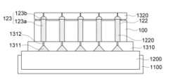
도 1은 본 발명의 일 실시예에 따른 표시 장치의 사시도이다.
도 2는 도 1의 I-I'을 따라 자른 단면도이다.
도 3은 도 1의 A를 확대한 평면도이다.
도 4는 도 3의 II-II'를 따라 자른 단면도이다.
도 5 및 도 6은 도 3의 II-II'를 따라 자른 다른 단면도이다.
도 7은 본 발명의 다른 일 실시예에 따른 표시 장치의 사시도이다.
도 8은 도 7의 III-III'을 따라 자른 단면도이다.
도 9은 도 8의 C부분을 확대한 확대도이다.
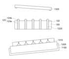
도 10 내지 도 14는 본 발명의 일 실시예에 따른 표시 장치의 제조 방법을 나타낸 도면이다.FIG. 1 is a perspective view of a display device according to one embodiment of the present invention.
Figure 2 is a cross-sectional view taken along line I-I' of Figure 1.
Figure 3 is an enlarged plan view of A in Figure 1.
Figure 4 is a cross-sectional view taken along line II-II' of Figure 3.
Figures 5 and 6 are other cross-sectional views taken along line II-II' of Figure 3.
Figure 7 is a perspective view of a display device according to another embodiment of the present invention.
Figure 8 is a cross-sectional view taken along line III-III' of Figure 7.
Figure 9 is an enlarged view of section C of Figure 8.
FIGS. 10 to 14 are drawings showing a method for manufacturing a display device according to one embodiment of the present invention.
본 발명의 이점 및 특징, 그리고 그것들을 달성하는 방법은 첨부되는 도면과 함께 상세하게 후술되어 있는 실시예들을 참조하면 명확해질 것이다. 그러나 본 발명은 이하에서 개시되는 실시예들에 한정되는 것이 아니라 서로 다른 다양한 형태로 구현될 것이며, 단지 본 실시예들은 본 발명의 개시가 완전하도록 하며, 본 발명이 속하는 기술분야에서 통상의 지식을 가진 자에게 발명의 범주를 완전하게 알려주기 위해 제공되는 것이며, 본 발명은 청구항의 범주에 의해 정의될 뿐이다. 따라서, 몇몇 실시예에서, 잘 알려진 공정 단계들, 잘 알려진 소자 구조 및 잘 알려진 기술들은 본 발명이 모호하게 해석되는 것을 피하기 위하여 구체적으로 설명되지 않는다. 명세서 전체에 걸쳐 동일 참조 부호는 동일 구성 요소를 지칭한다.The advantages and features of the present invention, and the methods for achieving them, will become apparent by referring to the embodiments described in detail below together with the accompanying drawings. However, the present invention is not limited to the embodiments disclosed below, but may be implemented in various different forms, and the present embodiments are provided only to make the disclosure of the present invention complete and to fully inform those skilled in the art of the scope of the invention, and the present invention is defined only by the scope of the claims. Accordingly, in some embodiments, well-known process steps, well-known device structures, and well-known techniques are not specifically described in order to avoid ambiguity in the interpretation of the present invention. Like reference numerals refer to like elements throughout the specification.
도면에서 여러 층 및 영역을 명확하게 표현하기 위하여 두께를 확대하여 나타내었다. 명세서 전체를 통하여 유사한 부분에 대해서는 동일한 도면 부호를 붙였다. 층, 막, 영역, 판 등의 부분이 다른 부분 "위에" 있다고 할 때, 이는 다른 부분 "바로 위에" 있는 경우뿐 아니라 그 중간에 또 다른 부분이 있는 경우도 포함한다. 반대로 어떤 부분이 다른 부분 "바로 위에" 있다고 할 때에는 중간에 다른 부분이 없는 것을 뜻한다. 또한, 층, 막, 영역, 판 등의 부분이 다른 부분 "아래에" 있다고 할 때, 이는 다른 부분 "바로 아래에" 있는 경우뿐 아니라 그 중간에 또 다른 부분이 있는 경우도 포함한다. 반대로 어떤 부분이 다른 부분 "바로 아래에" 있다고 할 때에는 중간에 다른 부분이 없는 것을 뜻한다.In order to clearly represent various layers and regions in the drawings, the thicknesses are enlarged and shown. Similar parts are designated by the same drawing reference numerals throughout the specification. When a part such as a layer, film, region, or plate is said to be "over" another part, this includes not only the case where it is "directly over" the other part, but also the case where there is another part in between. Conversely, when a part is said to be "directly over" another part, it means that there is no other part in between. Furthermore, when a part such as a layer, film, region, or plate is said to be "under" another part, this includes not only the case where it is "directly under" the other part, but also the case where there is another part in between. Conversely, when a part is said to be "directly under" another part, it means that there is no other part in between.
공간적으로 상대적인 용어인 "아래(below)", "아래(beneath)", "하부(lower)", "위(above)", "상부(upper)" 등은 도면에 도시되어 있는 바와 같이 하나의 소자 또는 구성 요소들과 다른 소자 또는 구성 요소들과의 상관관계를 용이하게 기술하기 위해 사용될 수 있다. 공간적으로 상대적인 용어는 도면에 도시되어 있는 방향에 더하여 사용시 또는 동작시 소자의 서로 다른 방향을 포함하는 용어로 이해되어야 한다. 예를 들면, 도면에 도시되어 있는 소자를 뒤집을 경우, 다른 소자의 "아래(below)"또는 "아래(beneath)"로 기술된 소자는 다른 소자의 "위(above)"에 놓여질 수 있다. 따라서, 예시적인 용어인 "아래"는 아래와 위의 방향을 모두 포함할 수 있다. 소자는 다른 방향으로도 배향될 수 있고, 이에 따라 공간적으로 상대적인 용어들은 배향에 따라 해석될 수 있다.The spatially relative terms "below," "beneath," "lower," "above," "upper," and the like can be used to easily describe the relationship of one element or component to another element or component, as depicted in the drawings. The spatially relative terms should be understood to include different orientations of the elements during use or operation in addition to the orientations depicted in the drawings. For example, if an element depicted in the drawings is flipped over, an element described as "below" or "beneath" another element may end up being placed "above" the other element. Thus, the exemplary term "below" can include both the above and below orientations. The elements may also be oriented in other directions, and the spatially relative terms may be interpreted accordingly.
본 명세서에서 어떤 부분이 다른 부분과 연결되어 있다고 할 때, 이는 직접적으로 연결되어있는 경우뿐 아니라, 그 중간에 다른 소자를 사이에 두고 전기적으로 연결되어 있는 경우도 포함한다. 또한, 어떤 부분이 어떤 구성 요소를 포함한다고 할 때, 이는 특별히 그에 반대되는 기재가 없는 한 다른 구성요소를 제외하는 것이 아니라 다른 구성요소를 더 포함할 수 있는 것을 의미한다.In this specification, when a part is said to be connected to another part, this includes not only cases where they are directly connected, but also cases where they are electrically connected with another element in between. In addition, when a part is said to include a certain component, this does not mean that other components are excluded, but that other components can be included, unless there is a specific description to the contrary.
본 명세서에서 제 1, 제 2, 제 3 등의 용어는 다양한 구성 요소들을 설명하는데 사용될 수 있지만, 이러한 구성 요소들은 상기 용어들에 의해 한정되는 것은 아니다. 상기 용어들은 하나의 구성 요소를 다른 구성 요소들로부터 구별하는 목적으로 사용된다. 예를 들어, 본 발명의 권리 범위로부터 벗어나지 않고, 제 1 구성 요소가 제 2 또는 제 3 구성 요소 등으로 명명될 수 있으며, 유사하게 제 2 또는 제 3 구성 요소도 교호적으로 명명될 수 있다.Although the terms first, second, third, etc. may be used in this specification to describe various components, these components are not limited by these terms. These terms are used for the purpose of distinguishing one component from other components. For example, without departing from the scope of the present invention, the first component may be referred to as the second or third component, etc., and similarly, the second or third component may also be referred to interchangeably.
다른 정의가 없다면, 본 명세서에서 사용되는 모든 용어(기술 및 과학적 용어를 포함)는 본 발명이 속하는 기술분야에서 통상의 지식을 가진 자에게 공통적으로 이해될 수 있는 의미로 사용될 수 있을 것이다. 또 일반적으로 사용되는 사전에 정의되어 있는 용어들은 명백하게 특별히 정의되어 있지 않은 한 이상적으로 또는 과도하게 해석되지 않는다.Unless otherwise defined, all terms (including technical and scientific terms) used in this specification may be used with a meaning that can be commonly understood by a person of ordinary skill in the art to which the present invention belongs. In addition, terms defined in commonly used dictionaries shall not be ideally or excessively interpreted unless explicitly specifically defined.
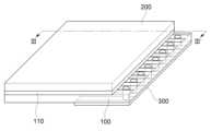
도 1은 본 발명의 일 실시예에 따른 표시 장치의 사시도이고, 도 2는 도 1의 I-I'을 따라 자른 단면도이다.FIG. 1 is a perspective view of a display device according to one embodiment of the present invention, and FIG. 2 is a cross-sectional view taken along line I-I' of FIG. 1.
본 발명의 실시예에 따른 표시 장치는, 도 1 및 도 2에 도시된 바와 같이, 제1 기판(100), 디스플레이층(110), 편광 필름(200), 연성 회로 기판(300)을 포함한다.A display device according to an embodiment of the present invention includes a first substrate (100), a display layer (110), a polarizing film (200), and a flexible circuit board (300), as shown in FIGS. 1 and 2.
제1 기판(100)은 표시 영역(DA) 및 패드 영역(PA)을 갖는다. 제1 기판(100)의 표시 영역(DA) 상에 디스플레이층(110)이 배치된다. 도시되지 않았지만, 표시 영역(DA)에 배치된 디스플레이층(110)은 게이트 라인들 및 데이터 라인들 및 게이트 라인들 및 데이터 라인들과 연결된 복수의 화소들을 포함한다. 화소는 스위칭 소자, 화소 전극 및 공통 전극을 포함할 수 있다. 스위칭 소자는 게이트 라인에 연결된 게이트 전극, 데이터 라인에 연결된 소스 전극 및 화소 전극에 연결된 드레인 전극을 포함할 수 있다. 스위칭 소자는 박막 트랜지스터로도 불린다.A first substrate (100) has a display area (DA) and a pad area (PA). A display layer (110) is arranged on the display area (DA) of the first substrate (100). Although not shown, the display layer (110) arranged on the display area (DA) includes gate lines and data lines and a plurality of pixels connected to the gate lines and data lines. The pixels may include a switching element, a pixel electrode, and a common electrode. The switching element may include a gate electrode connected to the gate line, a source electrode connected to the data line, and a drain electrode connected to the pixel electrode. The switching element is also called a thin film transistor.
공통 전극은 제2 기판에 위치할 수 있으며, 공통 전극과 화소 전극 사이에 전술된 액정층 또는 유기 발광층이 위치할 수 있다. 한편, 공통 전극은 제1 기판(100)에 위치할 수도 있다.The common electrode may be located on the second substrate, and the liquid crystal layer or organic light-emitting layer described above may be located between the common electrode and the pixel electrode. Meanwhile, the common electrode may also be located on the first substrate (100).
또한, 도시되지 않았지만, 화소는 컬러 필터 및 차광층을 더 포함할 수 있으며, 컬러 필터 및 차광층은 제1 기판 또는 제2 기판에 위치할 수 있다.Additionally, although not shown, the pixel may further include a color filter and a shading layer, and the color filter and the shading layer may be located on the first substrate or the second substrate.
도시되지 않았지만, 각 게이트 라인은 게이트 구동부에 연결된다. 게이트 구동부는 게이트 신호들을 생성하고, 그 게이트 신호들을 게이트 라인들에 차례로 공급한다.Although not shown, each gate line is connected to a gate driver. The gate driver generates gate signals and supplies the gate signals to the gate lines in sequence.
표시 영역(DA)에 위치하는 복수의 데이터 라인들은 게이트 라인들과 교차하고, 각 데이터 라인은 패드 단자(121) 중 하나에 연결될 수 있다.A plurality of data lines located in the display area (DA) intersect the gate lines, and each data line can be connected to one of the pad terminals (121).
제1 링크 라인(LK1)은 표시 영역(DA)에 위치하는 복수의 데이터 라인으로부터 패드 단자(121)까지 연장되어 데이터 라인과 패드 단자(121)를 전기적으로 연결할 수 있다. 구체적으로, 제1 링크 라인(LK1)은 패드 영역(PA)에서 제1 기판(100)의 상면의 데이터 라인과 패드 단자(121) 사이에 배치되고, 데이터 라인과 패드 단자(121)와 일체로 이루어질 수 있다.The first link line (LK1) can extend from a plurality of data lines located in the display area (DA) to the pad terminal (121) and electrically connect the data line and the pad terminal (121). Specifically, the first link line (LK1) is arranged between the data line and the pad terminal (121) on the upper surface of the first substrate (100) in the pad area (PA), and can be formed integrally with the data line and the pad terminal (121).
각 데이터 라인은 제1 링크 라인(LK1)을 통해 패드 단자(121)에 연결될 수 있다. 제1 링크 라인(LK1)은 각 데이터 라인으로부터 연장되고, 제1 링크 라인(LK1)은 패드 영역(PA)에 배치된다. 제1 링크 라인(LK1)은 각 데이터 라인과 평행하게 연장될 수 있고, 제1 링크 라인(LK1)은 각 데이터 라인으로부터 각도를 갖도록 연장될 수도 있다.Each data line can be connected to a pad terminal (121) via a first link line (LK1). The first link line (LK1) extends from each data line, and the first link line (LK1) is arranged in a pad area (PA). The first link line (LK1) can extend parallel to each data line, and the first link line (LK1) can also extend at an angle from each data line.
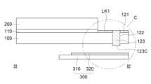
도 2에 도시된 바와 같이, 패드 단자(121)는 패드 영역(PA)에 위치하는 제1 링크 라인(LK1)의 단부로 정의한다. 패드 단자(121)는 제1 링크 라인(LK1)보다 더 큰 폭을 가질 수 있다. 이에 대해서는 도 3을 참조하여 상세히 설명한다.As illustrated in FIG. 2, the pad terminal (121) is defined as an end of the first link line (LK1) located in the pad area (PA). The pad terminal (121) may have a wider width than the first link line (LK1). This will be described in detail with reference to FIG. 3.
본 발명의 실시예에 따르면, 비아홀(122)은 패드 단자(121)에 위치할 수 있고, 연결 금속(123)은 비아홀(122)을 충진하고, 표시 영역(DA)에 배치된 화소와 연성 회로 기판(300)를 연결할 수 있다.According to an embodiment of the present invention, a via hole (122) may be located at a pad terminal (121), and a connecting metal (123) may fill the via hole (122) and connect a pixel arranged in a display area (DA) and a flexible circuit board (300).
도 2에 도시된 바와 같이, 제2 링크 라인(LK2)은 패드 영역(PA)에서 제1 기판(100)의 하면에 위치한다. 구체적으로, 제2 링크 라인(LK2)은 제1 기판(100)의 하면에 배치된 후술할 연성 회로 기판(300)의 제1 리드 라인(320)과 전기적으로 연결될 수 있다. 이때, 제2 링크 라인(LK2)은 제1 기판(100)을 사이에 두고 제1 링크 라인(LK1)과 서로 대향하여 배치될 수 있다.As illustrated in FIG. 2, the second link line (LK2) is positioned on the lower surface of the first substrate (100) in the pad area (PA). Specifically, the second link line (LK2) may be electrically connected to the first lead line (320) of the flexible circuit board (300) to be described later, which is positioned on the lower surface of the first substrate (100). At this time, the second link line (LK2) may be positioned opposite the first link line (LK1) with the first substrate (100) interposed therebetween.
제2 링크 라인(LK2)은 패드 단자(121) 및 제1 링크 라인(LK1)과 전기적으로 연결된다. 구체적으로, 제2 링크 라인(LK2)은 연결 금속(123)과 직접 접촉하여 전기적으로 연결되고, 연결 금속(123)과 연결된 패드 단자(121) 및 제1 링크 라인(LK1)과 전기적으로 연결된다.The second link line (LK2) is electrically connected to the pad terminal (121) and the first link line (LK1). Specifically, the second link line (LK2) is electrically connected by direct contact with the connecting metal (123), and is electrically connected to the pad terminal (121) and the first link line (LK1) connected to the connecting metal (123).
도시되지 않았지만, 제1 기판(100) 상에 제2 기판이 배치될 수 있다. 또한, 도시되지 않았지만, 제1 기판(100) 상에 액정층 또는 유기 발광층이 더 위치할 수 있다. 다만 이에 한정되는 것을 아니며, 제1 기판(100)과 제2 기판 사이에 액정층 또는 유기 발광층이 더 위치할 수 있다.Although not shown, a second substrate may be placed on the first substrate (100). Also, although not shown, a liquid crystal layer or an organic light-emitting layer may be further positioned on the first substrate (100). However, this is not limited thereto, and a liquid crystal layer or an organic light-emitting layer may be further positioned between the first substrate (100) and the second substrate.
본 발명의 실시예에 따르면, 제1 기판(100)은 보로실리케이트 글라스(glass), 소다 라임 글라스, 석영, Pyrex 중 적어도 하나로 이루어진다. 이에 따라, 레이저 공정에 의해 제1 기판(100)이 받는 영향을 최소화할 수 있다. 구체적으로, 글라스(glass)로 이루어진 제1 기판(100)은 내열성이 높아 레이저 공정에 의해 발생하는 열로 인한 변형 및 이에 따른 박리를 최소화할 수 있다.According to an embodiment of the present invention, the first substrate (100) is made of at least one of borosilicate glass, soda lime glass, quartz, and Pyrex. Accordingly, the influence of the laser process on the first substrate (100) can be minimized. Specifically, the first substrate (100) made of glass has high heat resistance, so that deformation and peeling due to heat generated by the laser process can be minimized.
본 발명의 실시예에 따르면, 편광 필름(200)은 제1 기판(100)의 표시 영역(DA) 상에 배치될 수 있다. 구체적으로, 편광 필름(200)은 제1 기판(100)의 표시 영역(DA)에 배치되고, 패드 영역(PA)에는 배치되지 않을 수 있다. 특히, 편광 필름(200)은 패드 영역(PA)에 배치된 비아홀(122)과 평면상에서 이격되어 배치될 수 있다. 이에 따라, 편광 필름(200)은 비아홀(122)을 충진시키기 위해 진행되는 레이저 공정에 의한 영향을 최소화할 수 있다. 구체적으로, 편광 필름(200)이 레이저 공정에 의해 발생하는 열에 의해 변형되는 것을 방지할 수 있다. 이에 대해서는, 도 3 내지 도 6을 참조하여 상세히 설명한다.According to an embodiment of the present invention, the polarizing film (200) may be placed on the display area (DA) of the first substrate (100). Specifically, the polarizing film (200) may be placed on the display area (DA) of the first substrate (100) and may not be placed on the pad area (PA). In particular, the polarizing film (200) may be placed spaced apart from the via hole (122) placed on the pad area (PA) on a plane. Accordingly, the polarizing film (200) may minimize the influence of the laser process performed to fill the via hole (122). Specifically, the polarizing film (200) may be prevented from being deformed by heat generated by the laser process. This will be described in detail with reference to FIGS. 3 to 6.
연성 회로 기판(300)은 제1 기판(100)의 하면에 배치되고, 연성 회로 기판(300)은 제2 링크 라인(LK2)과 연결되고, 제2 링크 라인(LK2)과 연결된 연결 금속(123)을 통해 패드 단자(121) 및 제1 링크 라인(LK1)과 연결된다. 이에 따라, 본 발명에 따른 표시 장치는 얇은 베젤을 가질 수 있다.A flexible circuit board (300) is placed on the lower surface of the first substrate (100), and the flexible circuit board (300) is connected to the second link line (LK2), and is connected to the pad terminal (121) and the first link line (LK1) through a connecting metal (123) connected to the second link line (LK2). Accordingly, the display device according to the present invention can have a thin bezel.
연성 회로 기판(300)은 기저층(310), 제1 리드 라인(320), 제2 리드 라인 및 피복층을 포함할 수 있다. 기저층(310)은 폴리 이미드(poly imide)로 이루어질 수 있다. 제1 리드 라인(320)은 전술된 연결 금속(123)과 전기적으로 연결될 수 있다. 구체적으로, 제1 리드 라인(320)은 연결 금속(123)과 직접 접촉한 제2 링크 라인(LK2)과 전기적으로 연결될 수 있다. 제2 리드 라인은 제1 리드 라인(320)과 전기적으로 연결될 수 있다. 구체적으로, 제2 리드 라인은 제1 리드 라인(320)과 일체로 형성될 수 있다. 피복층은 솔더 레지스트(solder resist)일 수 있다.The flexible circuit board (300) may include a base layer (310), a first lead line (320), a second lead line, and a covering layer. The base layer (310) may be made of poly imide. The first lead line (320) may be electrically connected to the aforementioned connecting metal (123). Specifically, the first lead line (320) may be electrically connected to a second link line (LK2) that is in direct contact with the connecting metal (123). The second lead line may be electrically connected to the first lead line (320). Specifically, the second lead line may be formed integrally with the first lead line (320). The covering layer may be a solder resist.
연성 회로 기판(300)은 테이프 캐리어 또는 가요성 인쇄 회로(FPC; Flexible Printed Circuit)일 수 있다.The flexible circuit board (300) may be a tape carrier or a flexible printed circuit (FPC).
도시되지 않았지만, 연성 회로 기판(300)은 구동 집적 회로를 더 포함할 수 있다. 즉, 구동 집적 회로는 표면 실장 기술(surface mounting technology)에 의해 연성 회로 기판(300)에 실장(mount)될 수 있다. 구동 집적 회로는 제1 리드 라인(320) 및 제2 리드 라인과 전기적으로 연결될 수 있다. 구동 집적 회로는 데이터 라인들로 영상 데이터 신호를 제공한다.Although not shown, the flexible circuit board (300) may further include a driver integrated circuit. That is, the driver integrated circuit may be mounted on the flexible circuit board (300) by surface mounting technology. The driver integrated circuit may be electrically connected to the first lead line (320) and the second lead line. The driver integrated circuit provides image data signals to the data lines.
이하, 도 3 내지 도 6을 참조하여, 본 발명의 실시예에 따른 편광 필름(200), 패드 단자(121), 비아홀(122) 및 연결 금속(123)에 대해 상세히 설명한다.Hereinafter, with reference to FIGS. 3 to 6, a polarizing film (200), a pad terminal (121), a via hole (122), and a connecting metal (123) according to an embodiment of the present invention will be described in detail.
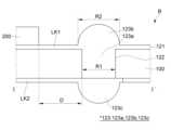
도 3은 도 1의 A를 확대한 확대도이고, 도 4는 도 3의 II-II`를 따라 자른 단면도이다. 도 5 및 도 6은 도 3의 II-II`를 따라 자른 다른 단면도이다.Fig. 3 is an enlarged view of A in Fig. 1, and Fig. 4 is a cross-sectional view taken along line II-II` in Fig. 3. Figs. 5 and 6 are other cross-sectional views taken along line II-II` in Fig. 3.
도 3을 참조하면, 표시 영역(DA)에 편광 필름(200)이 배치되고, 패드 영역(PA)에 제1 링크 라인(LK1), 패드 단자(121), 비아홀(122) 및 연결 금속(123)이 배치된다.Referring to FIG. 3, a polarizing film (200) is placed in the display area (DA), and a first link line (LK1), a pad terminal (121), a via hole (122), and a connecting metal (123) are placed in the pad area (PA).
도시되지 않았지만, 편광 필름(200)은 편광층 및 보호층을 포함할 수 있다. 편광층은 폴리 비닐 알코올계(Poly-Vinyl Alcohol, PVA) 필름을 포함할 수 있다. 구체적으로, 편광층은 폴리 비닐 알코올계 필름에 요오드와 같은 할로겐염 결정을 흡착시킨 후 PVA 필름을 특정 방향으로 연신시켜 요오드 결정들이 연신 방향에 나란히 정렬시켜 형성될 수 있다. 보호층은 트리아세틸셀룰로우스(TAC)와 같은 아세테이트계 수지, 폴리에스테르계 수지, 폴리이미드계 수지, 폴리오레핀계 수지, 아크릴계 수지, 폴리노르보르넨계 수지 중 적어도 하나를 포함할 수 있다. 이에 따라, 편광 필름은 폴리머 물질을 포함하기 때문에 내열성이 높지 않기 때문에 레이저 공정시 발생하는 열에 의해 편광 필름(200)이 변형되는 것을 방지하기 위해, 본 발명의 실시예에 따르면, 편광 필름(200)은 평면상에서 비아홀(122)과 0.5mm 이상 1.0mm 이하의 거리(D)로 이격되어 배치된다. 이때, 편광 필름(200)과 비아홀 사이의 거리를 패드 영역(PA)에 가장 가까이 위치한 편광 필름(200)의 일 측과 표시 영역(DA)에 가장 가까이 위치한 비아홀(122)의 가장자리 사이의 최단 거리로 정의할 수 있다. 즉, 편광 필름(200)과 비아홀 사이의 거리를 패드 영역(PA)에 가장 가까이 위치한 편광 필름(200)의 일 측과 표시 영역(DA)에 가장 가까이 위치한 비아홀(122)의 가장자리와 0.5mm 이상 1.0mm 이하의 최단 간격(D)으로 이격되어 배치된다.Although not shown, the polarizing film (200) may include a polarizing layer and a protective layer. The polarizing layer may include a polyvinyl alcohol (PVA) film. Specifically, the polarizing layer may be formed by adsorbing halogen salt crystals, such as iodine, onto a polyvinyl alcohol film and then stretching the PVA film in a specific direction so that the iodine crystals are aligned in a parallel manner in the stretching direction. The protective layer may include at least one of an acetate resin, such as triacetyl cellulose (TAC), a polyester resin, a polyimide resin, a polyolefin resin, an acrylic resin, and a polynorbornene resin. Accordingly, since the polarizing film does not have high heat resistance because it includes a polymer material, in order to prevent the polarizing film (200) from being deformed by the heat generated during the laser process, according to an embodiment of the present invention, the polarizing film (200) is disposed on a plane at a distance (D) of 0.5 mm or more and 1.0 mm or less from the via hole (122). At this time, the distance between the polarizing film (200) and the via hole can be defined as the shortest distance between the side of the polarizing film (200) located closest to the pad area (PA) and the edge of the via hole (122) located closest to the display area (DA). That is, the distance between the polarizing film (200) and the via hole is disposed at a shortest interval (D) of 0.5 mm or more and 1.0 mm or less from the side of the polarizing film (200) located closest to the pad area (PA) and the edge of the via hole (122) located closest to the display area (DA).
편광 필름(200)이 0.5mm 미만의 거리(D)로 비아홀(122)과 이격되는 경우, 비아홀(122)에 연결 금속(123)을 형성하기 위한 레이저 공정시 발생하는 열에 의해 편광 필름(200)이 변형되어 표시 품질의 저하를 발생시킬 수 있다, 편광 필름(200)이 1.0mm를 초과하는 최단 거리로 비아홀(122)과 이격되는 경우, 표시 장치의 베젤이 증가할 수 있다.If the polarizing film (200) is spaced from the via hole (122) by a distance (D) of less than 0.5 mm, the polarizing film (200) may be deformed by heat generated during a laser process for forming a connecting metal (123) in the via hole (122), which may cause a deterioration in display quality. If the polarizing film (200) is spaced from the via hole (122) by a minimum distance exceeding 1.0 mm, the bezel of the display device may increase.
편광 필름(200)은 외부에서 도달하는 광 중 특정 편광만 통과시키며, 나머지 광을 흡수 또는 차단시킬 수 있다. 또한, 도시되지 않았지만 제1 기판(100)의 하면에 별도의 편광 필름(200)이 배치될 수 있으며, 제1 기판(100)의 하면에 배치된 편광 필름(200)은 백라이트 유닛에서 출력되는 광 중에서 특정 편광만 통과시키거나, 나머지 광을 흡수 또는 차단시킬 수 있다.The polarizing film (200) can transmit only a specific polarization of light arriving from the outside, and absorb or block the remaining light. In addition, although not shown, a separate polarizing film (200) can be placed on the lower surface of the first substrate (100), and the polarizing film (200) placed on the lower surface of the first substrate (100) can transmit only a specific polarization of light output from the backlight unit, or absorb or block the remaining light.
제1 링크 라인(LK1)은 표시 영역(DA)에 배치된 게이트 라인(GL1 내지 GLi) 또는 데이터 라인(DL1 내지 DLj)으로부터 각각 연장된다. 이때, 패드 단자(121)는 패드 영역(PA)에 배치된 제1 링크 라인(LK1)의 단부이다. 이때, 패드 단자(121)는 연성 회로 기판(300) 및 구동 집적 회로(400)와 용이하게 연결되기 위해 제1 링크 라인(LK1)보다 큰 폭(W1<W2)을 가질 수 있다.The first link line (LK1) extends from each of the gate lines (GL1 to GLi) or data lines (DL1 to DLj) arranged in the display area (DA). At this time, the pad terminal (121) is an end of the first link line (LK1) arranged in the pad area (PA). At this time, the pad terminal (121) may have a width (W1<W2) greater than that of the first link line (LK1) in order to be easily connected to the flexible circuit board (300) and the driver integrated circuit (400).
본 발명의 실시예에 따르면, 비아홀(122)은 패드 단자(121)에 위치한다. 비아홀(122)은 제1 기판(100) 및 패드 단자(121)를 관통한다.According to an embodiment of the present invention, a via hole (122) is located in a pad terminal (121). The via hole (122) penetrates the first substrate (100) and the pad terminal (121).
도 3에 도시된 바와 같이, 비아홀(122)은 제1 링크 라인(LK1)의 폭(W1)보다 큰 직경(R1)을 갖는다(W1<R1). 이에 따라, 연결 금속(123)은 연성 회로 기판(300)의 제1 리드 라인(320)과 용이하게 연결될 수 있다. 또한, 비아홀(122)은 패드 단자(121)의 폭(W2)보다 작은 직경(R1)을 갖는다(W2>R1). 이에 따라, 패드 단자(121) 간의 전기적 연결을 방지할 수 있다.As illustrated in FIG. 3, the via hole (122) has a diameter (R1) larger than the width (W1) of the first link line (LK1) (W1<R1). Accordingly, the connecting metal (123) can be easily connected to the first lead line (320) of the flexible circuit board (300). In addition, the via hole (122) has a diameter (R1) smaller than the width (W2) of the pad terminal (121) (W2>R1). Accordingly, electrical connection between the pad terminals (121) can be prevented.
본 발명의 실시예에 따르면, 비아홀(122)에 배치된 연결 금속(123)은 제1 기판(100)의 상면과 하면을 연결하여 전도성 경로를 제공할 수 있다. 구체적으로, 연결 금속(123)은 비아홀(122)에 배치되어 제1 기판(100)의 상면에 배치된 화소들과 제1 기판(100)의 하면에 배치된 연성 회로 기판(300)을 연결한다. 게이트 라인 또는 데이터 라인은 표시 영역(DA)에 배치된 화소와 연결되고, 연결 금속(123)은 게이트 라인 또는 데이터 라인으로부터 연장된 패드 단자(121)와 전기적으로 연결되고, 연성 회로 기판(300)의 제1 리드 라인(320)과 전기적으로 연결된다. 예를 들어, 연결 금속(123)은 제1 기판(100)의 상면 및 비아홀(122)에서 데이터 라인으로부터 연장된 제1 링크 라인(LK1) 및 패드 단자(121)와 직접 접촉하여 전기적으로 연결되고, 제1 기판(100)의 하면 및 비아홀(122)에서 연성 회로 기판(300)의 제1 리드 라인(320)과 직접 접촉하여 전기적으로 연결될 수 있다.According to an embodiment of the present invention, a connecting metal (123) disposed in a via hole (122) can connect an upper surface and a lower surface of a first substrate (100) to provide a conductive path. Specifically, the connecting metal (123) is disposed in the via hole (122) to connect pixels disposed on an upper surface of the first substrate (100) and a flexible circuit board (300) disposed on a lower surface of the first substrate (100). A gate line or a data line is connected to a pixel disposed in a display area (DA), and the connecting metal (123) is electrically connected to a pad terminal (121) extended from the gate line or the data line and electrically connected to a first lead line (320) of the flexible circuit board (300). For example, the connecting metal (123) may be electrically connected by directly contacting the first link line (LK1) and the pad terminal (121) extended from the data line on the upper surface and via hole (122) of the first substrate (100), and may be electrically connected by directly contacting the first lead line (320) of the flexible circuit board (300) on the lower surface and via hole (122) of the first substrate (100).
연결 금속(123)은 비아홀(122) 내에 위치하는 연결부(123a), 제1 기판(100)의 상면으로부터 돌출된 제1 돌출부(123b)를 포함한다(도 4 내지 도 6 참조).The connecting metal (123) includes a connecting portion (123a) located within a via hole (122) and a first protrusion (123b) protruding from the upper surface of the first substrate (100) (see FIGS. 4 to 6).
도 4 내지 도 6을 참조하면, 연결 금속(123)의 연결부(123a)는 비아홀(122)에 의해 정의된 공간을 충진한다. 이에 따라, 연결부(123a)는 평면상에서 비아홀(122)과 실질적으로 동일한 직경(R1)을 가질 수 있다.Referring to FIGS. 4 to 6, the connecting portion (123a) of the connecting metal (123) fills the space defined by the via hole (122). Accordingly, the connecting portion (123a) can have a diameter (R1) substantially the same as the via hole (122) on a plane.
제1 돌출부(123b)는 제1 기판(100)의 상면 및 패드 단자(121)로부터 돌출된다. 도 4에 도시된 바와 같이, 제1 돌출부(123b)는 평면상에서 연결부(123a)보다 크거나 같은 직경을 가질 수 있다(R2>=R1). 이에 따라, 제1 돌출부(123b) 및 패드 단자(121)들은 서로 연결될 수 있는데, 제1 돌출부(123b)와 패드 단자(121)와의 접촉 면적이 증가하여 패드 단자(121)와 용이하게 연결될 수 있다. 다만 이에 한정되는 것은 아니며, 제1 돌출부(123b)는 평면상에서 연결부(123a)보다 작거나 같은 직경(R3<=R1)을 가질 수도 있다. 이에 따라, 제1 돌출부(123b) 및 패드 단자(121)들은 서로 연결되지 않을 수 있다.The first protrusion (123b) protrudes from the upper surface of the first substrate (100) and the pad terminal (121). As illustrated in FIG. 4, the first protrusion (123b) may have a diameter that is greater than or equal to a connecting portion (123a) in a plane (R2>=R1). Accordingly, the first protrusion (123b) and the pad terminal (121) may be connected to each other, and the contact area between the first protrusion (123b) and the pad terminal (121) increases, so that the first protrusion (123b) may be easily connected to the pad terminal (121). However, the present invention is not limited thereto, and the first protrusion (123b) may have a diameter that is less than or equal to a connecting portion (123a) in a plane (R3<=R1). Accordingly, the first protrusion (123b) and the pad terminal (121) may not be connected to each other.
도 4에 도시된 바와 같이, 제1 돌출부(123b)는 제1 기판(100) 및 패드 단자(121)로부터 돌출되어 반구 형태로 이루어질 수 있다. 또는, 도 5에 도시된 바와 같이, 제1 돌출부(123b)는 삼각뿔, 사각뿔과 같은 다각뿔 또는 원뿔의 형태로 이루어질 수 있다. 또는, 도 6에 도시된 바와 같이, 제1 돌출부(123b)는 다각 기둥 또는 원 기둥의 형태로 이루어질 수 있다.As illustrated in FIG. 4, the first protrusion (123b) may be formed in a hemispherical shape by protruding from the first substrate (100) and the pad terminal (121). Alternatively, as illustrated in FIG. 5, the first protrusion (123b) may be formed in a polygonal pyramid, such as a triangular pyramid or a square pyramid, or a cone. Alternatively, as illustrated in FIG. 6, the first protrusion (123b) may be formed in a polygonal column or a circular column.
또한, 도 4 내지 도 6에 도시된 바와 같이, 연결 금속(123)은 제2 돌출부(123c)를 더 포함할 수 있다. 제2 돌출부(123c)는 제1 기판(100) 및 패드 단자(121)로부터 돌출된다. 구체적으로, 제2 돌출부(123c)는 제1 기판(100)의 하면으로부터 돌출된다. 제2 돌출부(123c)는 반구, 삼각뿔, 사각뿔과 같은 다각뿔, 원 기둥 또는 다각 기둥의 형태로 이루어질 수 있다.In addition, as illustrated in FIGS. 4 to 6, the connecting metal (123) may further include a second protrusion (123c). The second protrusion (123c) protrudes from the first substrate (100) and the pad terminal (121). Specifically, the second protrusion (123c) protrudes from the lower surface of the first substrate (100). The second protrusion (123c) may be formed in the shape of a polygonal pyramid such as a hemisphere, a triangular pyramid, a square pyramid, a circular column, or a polygonal column.
삭제delete
이하, 도 7 내지 도 9를 참조하여, 본 발명의 다른 실시예에 따른 표시 장치에 대해 상세히 설명한다.Hereinafter, a display device according to another embodiment of the present invention will be described in detail with reference to FIGS. 7 to 9.
도 7은 본 발명의 다른 일 실시예에 따른 표시 장치의 사시도이고, 도 8은 도 7의 III-III'을 따라 자른 단면도이고, 도 9은 도 8의 C부분을 확대한 확대도이다.FIG. 7 is a perspective view of a display device according to another embodiment of the present invention, FIG. 8 is a cross-sectional view taken along line III-III' of FIG. 7, and FIG. 9 is an enlarged view of portion C of FIG. 8.
본 발명의 다른 일 실시예에 따른 표시 장치에 관한 설명 가운데 본 발명의 일 실시예에 따른 표시 장치에 관한 설명과 중복되는 내용은 생략한다.본 발명의 다른 일 실시예에 따르면, 연성 회로 기판(300)의 제1 리드 라인(320)은 연결 금속(123)과 전기적으로 연결된다. 구체적으로, 연성 회로 기판(300)의 제1 리드 라인(320)은 연결 금속(123)과 직접 접촉하여 전기적으로 연결된다.In the description of the display device according to another embodiment of the present invention, any content that overlaps with the description of the display device according to another embodiment of the present invention will be omitted. According to another embodiment of the present invention, the first lead line (320) of the flexible circuit board (300) is electrically connected to the connecting metal (123). Specifically, the first lead line (320) of the flexible circuit board (300) is in direct contact with the connecting metal (123) and is electrically connected thereto.
본 발명의 다른 일 실시예에 따르면, 연성 회로 기판(300)은 연결 금속(123)과 연결된 제1 링크 라인(LK1)과 중첩할 수 있다. 구체적으로, 제1 리드 라인(320)은 연결 금속(123)과 연결된 제1 링크 라인(LK1)과 중첩할 수 있다. 이에 따라, 제1 리드 라인(320)은 제1 기판(100)을 사이에 두고 제1 링크 라인(LK1)과 서로 대향하여 배치할 수 있다.According to another embodiment of the present invention, the flexible circuit board (300) may overlap the first link line (LK1) connected to the connecting metal (123). Specifically, the first lead line (320) may overlap the first link line (LK1) connected to the connecting metal (123). Accordingly, the first lead line (320) may be arranged to face the first link line (LK1) with the first board (100) interposed therebetween.
삭제delete
이하, 도 10 내지 도 14를 참조하여, 본 발명의 일 실시예에 따른 표시 장치의 제조 방법에 대해 상세히 설명한다.Hereinafter, with reference to FIGS. 10 to 14, a method for manufacturing a display device according to one embodiment of the present invention will be described in detail.
도 10 내지 도 14는 본 발명의 일 실시예에 따른 표시 장치의 제조 방법을 나타낸 도면이다.FIGS. 10 to 14 are drawings showing a method for manufacturing a display device according to one embodiment of the present invention.
도시되지 않았지만, 제1 기판(100)의 표시 영역(DA)에 게이트 라인 및 데이터 라인과 연결된 화소를 형성하고, 패드 영역(PA)에 제1 링크 라인(LK1) 및 패드 단자(121)가 형성된다. 이때, 제1 기판(100) 상에 제2 기판이 배치될 수 있다. 다만, 이에 한정되지 않는다. 또한, 제1 기판(100)의 표시 영역(DA)에 배치된 디스플레이층(110)과 중첩하도록 편광 필름(200)이 배치되고, 패드 단자(121)에 제1 기판(100)을 관통하는 비아홀(122)이 형성한다.Although not shown, pixels connected to gate lines and data lines are formed in the display area (DA) of the first substrate (100), and a first link line (LK1) and a pad terminal (121) are formed in the pad area (PA). At this time, a second substrate may be placed on the first substrate (100). However, the present invention is not limited thereto. In addition, a polarizing film (200) is placed so as to overlap with the display layer (110) placed in the display area (DA) of the first substrate (100), and a via hole (122) penetrating the first substrate (100) is formed in the pad terminal (121).
이후, 비아홀(122)을 충진하는 연결 금속(123)을 형성하기 위한 공정이 진행된다.Afterwards, a process is performed to form a connecting metal (123) that fills the via hole (122).
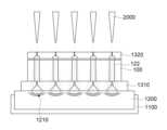
구체적으로, 도 10을 참조하면, 고체의 연결 금속 물질(1200) 및 노즐 글라스(1310)가 가압 유닛(1100) 상에 배치되고, 편광 필름(200)을 포함하는 표시 패널이 노즐 글라스(1310) 상에 배치된다. 구체적으로, 노즐 글라스(1310) 상에 비아홀(122)이 형성된 제1 기판(100)이 노즐 글라스(1310) 상에 배치된다. 제1 기판(100)을 포함하는 표시 패널 상에 커버 글라스(1320)가 배치된다.Specifically, referring to FIG. 10, a solid connecting metal material (1200) and a nozzle glass (1310) are placed on a pressurizing unit (1100), and a display panel including a polarizing film (200) is placed on the nozzle glass (1310). Specifically, a first substrate (100) having a via hole (122) formed on the nozzle glass (1310) is placed on the nozzle glass (1310). A cover glass (1320) is placed on the display panel including the first substrate (100).
가압 유닛(1100)은 가압 유닛(1100) 상에 배치된 연결 금속 물질(1200)에 압력을 가할 수 있다.The pressurizing unit (1100) can apply pressure to a connecting metal material (1200) placed on the pressurizing unit (1100).
연결 금속 물질(1200)은 금속으로 이루어질 수 있다. 구체적으로, 연결 금속 물질(1200)은 저융점 금속(In, Sn, Zn, Pb 등) 또는 저융점 금속 합금(PbSn, InSn 등) 중 적어도 하나를 포함할 수 있다. 이에 따라, 비아홀 충진을 위한 레이저 공정시 높은 온도가 요구되지 않기 때문에, 레이저에 의해 발생하는 열이 제1 기판(100) 및 편광 필름(200)을 포함하는 표시 패널에 영향을 미치는 것을 최소화할 수 있다.The connecting metal material (1200) may be made of a metal. Specifically, the connecting metal material (1200) may include at least one of a low-melting-point metal (In, Sn, Zn, Pb, etc.) or a low-melting-point metal alloy (PbSn, InSn, etc.). Accordingly, since a high temperature is not required during a laser process for filling a via hole, the heat generated by the laser can be minimized from affecting the display panel including the first substrate (100) and the polarizing film (200).
제1 기판(100)의 하면 및 상면에 각각 배치된 노즐 글라스(1310) 및 커버 글라스(1320)는 보로실리케이트 글라스(glass), 소다 라임 글라스, 석영, Pyrex 중 적어도 하나로 이루어질 수 있다. 이에 따라, 노즐 글라스(1310) 및 커버 글라스(1320)는 투명하기 때문에 커버 글라스(1320) 상에서 조사되는 레이저가 투과되어 연결 금속 물질을 융융시킬 수 있고, 노즐 글라스(1310) 및 커버 글라스(1320)는 내열성이 높기 때문에 레이저에 의해 발생하는 열에 의해 변형되는 것을 최소화할 수 있다.The nozzle glass (1310) and the cover glass (1320) respectively arranged on the lower and upper surfaces of the first substrate (100) may be made of at least one of borosilicate glass, soda lime glass, quartz, and Pyrex. Accordingly, since the nozzle glass (1310) and the cover glass (1320) are transparent, the laser irradiated on the cover glass (1320) may be transmitted through and melt the connecting metal material, and since the nozzle glass (1310) and the cover glass (1320) have high heat resistance, the deformation caused by the heat generated by the laser may be minimized.
노즐 글라스(1310)는 노즐 글라스(1310)의 상면과 하면을 관통하는 노즐이 형성될 수 있다. 구체적으로, 노즐 글라스(1310)의 하면에 위치하는 노즐(1311)은 점점 폭이 작아지는 형태를 가지고, 노즐 글라스(1310)의 상면에 위치하는 오리피스(orifice) 노즐(1312)은 노즐 글라스(1310)의 하면에 위치하는 노즐과 연결되며 노즐 글라스(1310)의 하면에 위치하는 노즐의 가장 작은 폭과 같은 폭을 가질 수 있다. 이에 따라, 노즐 글라스(1310)의 노즐(1311, 1312)을 통과하는 유체의 모세관 현상이 촉진시킬 수 있다. 이에 대해서는 도 10을 참조하여 상세히 설명한다.The nozzle glass (1310) may be formed with a nozzle that penetrates the upper and lower surfaces of the nozzle glass (1310). Specifically, the nozzle (1311) located on the lower surface of the nozzle glass (1310) has a shape in which the width gradually decreases, and the orifice nozzle (1312) located on the upper surface of the nozzle glass (1310) is connected to the nozzle located on the lower surface of the nozzle glass (1310) and may have the same width as the smallest width of the nozzle located on the lower surface of the nozzle glass (1310). Accordingly, the capillary phenomenon of the fluid passing through the nozzles (1311, 1312) of the nozzle glass (1310) may be promoted. This will be described in detail with reference to FIG. 10.
고체의 연결 금속 물질(1200) 상에 노즐 글라스(1310), 표시 패널 및 커버 글라스(1320)를 순차적으로 적층한 후, 커버 글라스(1320) 상에서 레이저(2000)를 고체의 연결 금속 물질(1200)에 조사하고, 고체의 연결 금속 물질(1200)은 부분적으로 융융되어 액체화된 연결 금속 물질(1210)이 될 수 있다. 이때, 레이저에 의해 발생하는 열이 발생하는 면적을 최소화하기 위해 극초단파 레이저(Ultrashort Pulse Laser)를 사용할 수 있다.After sequentially stacking a nozzle glass (1310), a display panel, and a cover glass (1320) on a solid connecting metal material (1200), a laser (2000) is irradiated on the solid connecting metal material (1200) on the cover glass (1320), and the solid connecting metal material (1200) can be partially melted to become a liquefied connecting metal material (1210). At this time, an ultrashort pulse laser can be used to minimize the area where heat generated by the laser is generated.
다음으로, 도 11을 참조하면, 비아홀(122)이 형성된 제1 기판(100)이 배치된 공간에서 진공을 형성하고, 가압 유닛(1100)은 연결 금속 물질(1200)에 압력을 가한다. 이에 따라, 도 12에 도시된 바와 같이, 부분적으로 융융되어 액체화된 연결 금속 물질(1210)은 제1 기판(100)의 상면과 하면 사이의 압력 차이에 의해 노즐 글라스(1310)의 노즐을 따라 제1 기판(100)의 비아홀(122)에 주입된다. 구체적으로, 융융되어 액체화된 연결 금속 물질(1210)은 제1 기판(100)의 하면에서 가압 유닛(1100)에 의해 가해진 압력과 제1 기판(100)의 상면의 진공과의 압력 차이에 의해 노즐 글라스(1310)의 노즐을 따라 제1 기판(100)의 비아홀(122)에 주입된다. 이때, 노즐 글라스(1310)의 노즐은 폭이 좁은 오리피스(orifice) 노즐을 포함할 수 있다. 이에 따라, 노즐 글라스(1310)의 노즐에서 모세관 현상이 촉진되어 융융되어 액체화된 연결 금속 물질(1210)이 빠르게 비아홀(122)로 주입될 수 있다.Next, referring to FIG. 11, a vacuum is formed in a space where a first substrate (100) in which a via hole (122) is formed is placed, and a pressurizing unit (1100) applies pressure to a connecting metal material (1200). Accordingly, as illustrated in FIG. 12, a connecting metal material (1210) that has been partially melted and liquefied is injected into the via hole (122) of the first substrate (100) along the nozzle of the nozzle glass (1310) by the pressure difference between the upper and lower surfaces of the first substrate (100). Specifically, the connecting metal material (1210) that has been melted and liquefied is injected into the via hole (122) of the first substrate (100) along the nozzle of the nozzle glass (1310) by the pressure difference between the pressure applied by the pressurizing unit (1100) on the lower surface of the first substrate (100) and the vacuum of the upper surface of the first substrate (100). At this time, the nozzle of the nozzle glass (1310) may include a narrow orifice nozzle. Accordingly, the capillary phenomenon is promoted in the nozzle of the nozzle glass (1310), so that the melted and liquefied connecting metal material (1210) can be quickly injected into the via hole (122).
이에 따라, 융융되어 액체화된 연결 금속 물질(1210)로 비아홀(122)이 충진되어 연결 금속(123)의 연결부(123a)를 형성하고, 융융되어 액체화된 연결 금속 물질(1210)로 커버 글라스(1320)의 하면까지 충진되어 연결 금속(123)의 제1 돌출부(123b)를 형성할 수 있다. 이에 따라, 커버 클라스의 하면의 형태에 따라 연결 금속 물질(1200)이 충진될 수 있다. 구체적으로, 커버 글라스(1320)의 하면은 반구, 다각뿔, 원뿔, 다각 기둥, 원기둥 형태의 오목부를 가져 융융되어 액체화된 연결 금속 물질(1210)은 반구 형태의 커버 글라스(1320) 하면의 오목부를 충진하여 제1 돌출부(123b)를 형성할 수 있다. 예를 들어, 도 13에 도시된 바와 같이, 커버 글라스(1320)의 하면은 반구 형태의 오목부를 가져 융융되어 액체화된 연결 금속 물질(1210)은 반구 형태의 커버 글라스(1320) 하면의 오목부를 충진하여 반구 형태의 제1 돌출부(123b)를 형성할 수 있다.Accordingly, the via hole (122) is filled with the melted and liquefied connecting metal material (1210) to form the connecting portion (123a) of the connecting metal (123), and the melted and liquefied connecting metal material (1210) can be filled up to the lower surface of the cover glass (1320) to form the first protrusion (123b) of the connecting metal (123). Accordingly, the connecting metal material (1200) can be filled according to the shape of the lower surface of the cover class. Specifically, the lower surface of the cover glass (1320) has a concave portion in the shape of a hemisphere, a polygonal pyramid, a cone, a polygonal pillar, or a cylinder, and the melted and liquefied connecting metal material (1210) can fill the concave portion of the lower surface of the cover glass (1320) in the shape of a hemisphere to form the first protrusion (123b). For example, as illustrated in FIG. 13, the lower surface of the cover glass (1320) has a hemispherical concave portion, and the melted and liquefied connecting metal material (1210) can fill the concave portion of the lower surface of the hemispherical cover glass (1320) to form a hemispherical first protrusion (123b).
다음으로, 제1 기판(100)의 상면에서 진공 및 제1 기판(100)의 하면에서 가해진 압력을 해제한다.Next, the vacuum applied to the upper surface of the first substrate (100) and the pressure applied to the lower surface of the first substrate (100) are released.
도 14를 참조하면, 표시 패널이 분리되어 표시 장치가 제조 된다. 구체적으로, 표시 패널은 제1 기판(100)의 하면에 배치된 가압 유닛(1100), 연결 금속 물질(1200) 및 제1 기판(100)의 상면에 배치된 커버 글라스(1320)와 분리된다.Referring to FIG. 14, a display device is manufactured by separating a display panel. Specifically, the display panel is separated from a pressurizing unit (1100) disposed on a lower surface of a first substrate (100), a connecting metal material (1200), and a cover glass (1320) disposed on an upper surface of the first substrate (100).
도시되지 않았지만, 제1 기판(100)을 포함한 표시 패널의 하면에 연성 회로 기판(300)을 배치하여 연결 금속(123)과 연성 회로 기판(300)의 제1 리드 라인(320)을 연결할 수 있다.Although not shown, a flexible circuit board (300) may be placed on the lower surface of the display panel including the first substrate (100) to connect the connecting metal (123) and the first lead line (320) of the flexible circuit board (300).
본 발명의 실시예에 따르면, 비아홀(122)에 배치된 연결 금속(123)은 제1 기판(100)의 상면과 하면을 연결하여 전도성 경로를 제공할 수 있다. 구체적으로, 연결 금속(123)은 비아홀(122)에 배치되어 제1 기판(100)의 상면에 배치된 화소들과 제1 기판(100)의 하면에 배치된 연성 회로 기판(300)을 연결한다. 예를 들어, 연결 금속(123)은 제1 기판(100)의 상면 및 비아홀(122)에서 데이터 라인으로부터 연장된 제1 링크 라인(LK1) 및 패드 단자(121)와 직접 접촉하여 전기적으로 연결되고, 제1 기판(100)의 하면 및 비아홀(122)에서 연성 회로 기판(300)의 제1 리드 라인(320)과 직접 접촉하여 전기적으로 연결될 수 있다.According to an embodiment of the present invention, the connecting metal (123) disposed in the via hole (122) can connect the upper surface and the lower surface of the first substrate (100) to provide a conductive path. Specifically, the connecting metal (123) is disposed in the via hole (122) to connect the pixels disposed on the upper surface of the first substrate (100) and the flexible circuit board (300) disposed on the lower surface of the first substrate (100). For example, the connecting metal (123) can be in direct contact with and electrically connected to the first link line (LK1) and the pad terminal (121) extended from the data line on the upper surface of the first substrate (100) and the via hole (122), and can be in direct contact with and electrically connected to the first lead line (320) of the flexible circuit board (300) on the lower surface of the first substrate (100) and the via hole (122).
또한, 연성 회로 기판(300)의 제2 리드 라인은 구동 집적 회로(400)와 연결되어, 연결 금속(123)은 구동 집적 회로(400)와 연결되어 구동 집적 회로(400)로부터 신호를 전달 받을 수 있다.In addition, the second lead line of the flexible circuit board (300) is connected to the driver integrated circuit (400), and the connecting metal (123) is connected to the driver integrated circuit (400) to receive a signal from the driver integrated circuit (400).
삭제delete
이상에서 설명한 본 발명은 상술한 실시예 및 첨부된 도면에 한정되는 것이 아니고, 본 발명의 기술적 사상을 벗어나지 않는 범위 내에서 여러 가지 치환, 변형 및 변경이 가능하다는 것이 본 발명이 속하는 기술 분야에서 통상의 지식을 가진 자에게 있어 명백할 것이다.The present invention described above is not limited to the above-described embodiments and the attached drawings, and it will be apparent to a person skilled in the art to which the present invention pertains that various substitutions, modifications, and changes are possible within a scope that does not depart from the technical spirit of the present invention.
100: 제1 기판200: 편광 필름
300: 연성 회로 기판400: 구동 집적 회로
1100: 가압 유닛1200: 연결 금속 물질
1310: 노즐 글라스1320: 커버 글라스100: 1st substrate 200: Polarizing film
300: Flexible circuit board 400: Drive integrated circuit
1100: Pressurized unit 1200: Connecting metal material
1310: Nozzle glass 1320: Cover glass
Claims (19)
Translated fromKorean가압 유닛, 고체의 연결 금속 물질, 노즐 글라스, 상기 제1 기판 및 편광 필름을 포함하는 표시 패널, 커버 글라스를 순차적으로 적층하는 단계;
상기 커버 글라스 상에서 고체의 연결 금속 물질에 레이저를 조사하여 고체의 연결 금속 물질을 부분적으로 액체화 시키는 단계;
표시 패널이 배치된 공간에 진공을 형성하고, 가압 유닛이 부분적으로 액체화된 연결 금속 물질에 압력을 가하는 단계;
비아홀 내부를 액체화된 연결 금속 물질을 충진하여 연결 금속의 연결부를 형성하고, 커버 글라스의 하면까지 액체화된 연결 금속 물질을 충진하여 연결 금속의 제1 돌출부를 형성하는 단계;
표시 패널이 배치된 공간에 형성된 진공 및 부분적으로 액체화된 연결 금속 물질에 가해진 압력을 해제하는 단계; 및
적층된 가압 유닛, 고체의 연결 금속 물질, 노즐 글라스, 상기 제1 기판 및 편광 필름을 포함하는 표시 패널, 커버 글라스를 분리하는 단계;를 포함하는 표시 장치 제조 방법.A step of forming a display panel by forming pixels in a display area of a first substrate, forming pad terminals and via holes in a pad area, and arranging a polarizing film to overlap with the display area of the first substrate;
A step of sequentially laminating a pressurized unit, a solid connecting metal material, a nozzle glass, a display panel including the first substrate and a polarizing film, and a cover glass;
A step of partially liquefying a solid connecting metal material by irradiating a laser to the solid connecting metal material on the cover glass;
A step of forming a vacuum in a space where the display panel is placed, and a pressurizing unit applying pressure to the partially liquefied connecting metal material;
A step of forming a connecting part of a connecting metal by filling the inside of a via hole with a liquefied connecting metal material, and forming a first protrusion of the connecting metal by filling the inside of a via hole with a liquefied connecting metal material up to the lower surface of a cover glass;
A step of releasing the vacuum formed in the space where the display panel is placed and the pressure applied to the partially liquefied connecting metal material; and
A method for manufacturing a display device, comprising: a step of separating a display panel including a laminated pressurized unit, a solid connecting metal material, a nozzle glass, the first substrate and a polarizing film, and a cover glass.
상기 노즐 글라스는 오리피스(orifice) 노즐을 포함하는 표시 장치 제조 방법.In Article 13,
The above nozzle glass is a method for manufacturing a display device including an orifice nozzle.
상기 커버 글라스의 하면은 반구, 다각뿔, 원뿔, 다각 기둥, 원기둥 형태 중 어느 하나의 형태의 오목부를 갖는 표시 장치 제조 방법.In Article 13,
A method for manufacturing a display device, wherein the lower surface of the cover glass has a concave portion in any one of the shapes of a hemisphere, a polyhedron, a cone, a polyhedron, and a cylinder.
상기 연결 금속의 연결부의 직경은 상기 연결 금속의 제1 돌출부의 직경보다 작은 표시 장치 제조 방법.In Article 13,
A method for manufacturing a display device, wherein the diameter of the connecting portion of the above connecting metal is smaller than the diameter of the first protrusion of the above connecting metal.
상기 제1 기판의 표시 영역에 화소를 형성하고, 패드 영역에 패드 단자 및 비아홀을 형성하고, 상기 제1 기판의 표시 영역과 중첩하여 편광 필름을 배치하여 표시 패널을 형성하는 단계는,
상기 화소와 연결되는 제1 링크 라인을 형성하고, 상기 제1 링크 라인과 연결되고 상기 제1 링크 라인보다 넓은 폭을 갖는 패드 단자를 형성하는 단계를 포함하고,
상기 연결 금속의 연결부의 직경은 상기 패드 단자의 폭보다 작은 표시 장치 제조 방법.In Article 13,
The step of forming a display panel by forming pixels in the display area of the first substrate, forming pad terminals and via holes in the pad area, and arranging a polarizing film to overlap with the display area of the first substrate is as follows.
A step of forming a first link line connected to the pixel, and forming a pad terminal connected to the first link line and having a wider width than the first link line,
A method for manufacturing a display device, wherein the diameter of the connecting portion of the above connecting metal is smaller than the width of the above pad terminal.
상기 레이저는 극초단파 레이저인 표시 장치 제조 방법.In Article 13,
A method for manufacturing a display device wherein the laser is an ultrashort wave laser.
상기 제1 기판은 보로실리케이트 글라스(glass), 소다 라임 글라스, 석영, Pyrex 중 적어도 하나로 이루어진 표시 장치 제조 방법.In Article 13,
A method for manufacturing a display device, wherein the first substrate is made of at least one of borosilicate glass, soda lime glass, quartz, and Pyrex.
Priority Applications (3)
| Application Number | Priority Date | Filing Date | Title |
|---|---|---|---|
| KR1020180141306AKR102799625B1 (en) | 2018-11-16 | 2018-11-16 | Display and manufacturing method of the same |
| US16/542,206US10980119B2 (en) | 2018-11-16 | 2019-08-15 | Display device and method of manufacturing the same |
| CN201911035123.8ACN111199914B (en) | 2018-11-16 | 2019-10-29 | Display Devices |
Applications Claiming Priority (1)
| Application Number | Priority Date | Filing Date | Title |
|---|---|---|---|
| KR1020180141306AKR102799625B1 (en) | 2018-11-16 | 2018-11-16 | Display and manufacturing method of the same |
Publications (2)
| Publication Number | Publication Date |
|---|---|
| KR20200057855A KR20200057855A (en) | 2020-05-27 |
| KR102799625B1true KR102799625B1 (en) | 2025-04-23 |
Family
ID=70726727
Family Applications (1)
| Application Number | Title | Priority Date | Filing Date |
|---|---|---|---|
| KR1020180141306AActiveKR102799625B1 (en) | 2018-11-16 | 2018-11-16 | Display and manufacturing method of the same |
Country Status (3)
| Country | Link |
|---|---|
| US (1) | US10980119B2 (en) |
| KR (1) | KR102799625B1 (en) |
| CN (1) | CN111199914B (en) |
Families Citing this family (1)
| Publication number | Priority date | Publication date | Assignee | Title |
|---|---|---|---|---|
| CN113539127B (en)* | 2021-07-09 | 2023-04-11 | 京东方科技集团股份有限公司 | Display substrate, preparation method thereof and display device |
Family Cites Families (34)
| Publication number | Priority date | Publication date | Assignee | Title |
|---|---|---|---|---|
| US6149774A (en)* | 1998-06-10 | 2000-11-21 | Delsys Pharmaceutical Corporation | AC waveforms biasing for bead manipulating chucks |
| US6952020B1 (en)* | 1999-07-06 | 2005-10-04 | Semiconductor Energy Laboratory Co., Ltd. | Semiconductor device and manufacturing method thereof |
| TWI285782B (en)* | 1999-09-08 | 2007-08-21 | Toshiba Matsushita Display Tec | Display device and method for producing the device |
| JP4280583B2 (en) | 2003-08-25 | 2009-06-17 | 新光電気工業株式会社 | Via formation method |
| KR101212149B1 (en)* | 2005-12-21 | 2012-12-14 | 엘지디스플레이 주식회사 | Multi-Domain Liquid Crystal Display Device and Method for Manufacturing the Same |
| US20080002460A1 (en)* | 2006-03-01 | 2008-01-03 | Tessera, Inc. | Structure and method of making lidded chips |
| JP2008112136A (en)* | 2006-10-04 | 2008-05-15 | Mitsubishi Electric Corp | Display device and manufacturing method thereof |
| US20080218678A1 (en)* | 2007-03-09 | 2008-09-11 | Koji Nakayama | Liquid crystal display device |
| KR20100065785A (en)* | 2008-12-08 | 2010-06-17 | 삼성전자주식회사 | A method of chip interconnection using a capillary motion |
| US20110255251A1 (en)* | 2009-01-30 | 2011-10-20 | Sharp Kabushiki Kaisha | Electronic package and display apparatus |
| KR101071180B1 (en) | 2009-04-03 | 2011-10-10 | 한국생산기술연구원 | Through Via hole filling apparatus and method |
| KR101021222B1 (en) | 2010-01-28 | 2011-03-11 | 한국생산기술연구원 | Metal peeling apparatus in wafer through via hole and peeling method using same |
| KR101215644B1 (en)* | 2010-12-01 | 2012-12-26 | 에스케이하이닉스 주식회사 | Semiconductor chip, package and method for manufacturing semiconductor chip |
| KR101910841B1 (en)* | 2012-03-27 | 2018-10-23 | 엘지디스플레이 주식회사 | Display device and manufacturing for method thereof |
| US20130293482A1 (en) | 2012-05-04 | 2013-11-07 | Qualcomm Mems Technologies, Inc. | Transparent through-glass via |
| US9214507B2 (en)* | 2012-08-17 | 2015-12-15 | Apple Inc. | Narrow border organic light-emitting diode display |
| US20140111496A1 (en)* | 2012-10-22 | 2014-04-24 | Apple Inc. | Displays with Circuitry for Compensating Parasitic Coupling Effects |
| JP6156044B2 (en)* | 2013-10-10 | 2017-07-05 | セイコーエプソン株式会社 | Liquid crystal device and electronic device |
| JP6244802B2 (en)* | 2013-10-11 | 2017-12-13 | セイコーエプソン株式会社 | Electro-optical device and electronic apparatus |
| JP2016099492A (en)* | 2014-11-21 | 2016-05-30 | セイコーエプソン株式会社 | Liquid crystal device and electronic apparatus |
| US9535522B2 (en)* | 2014-12-22 | 2017-01-03 | Lg Display Co., Ltd. | Flexible organic light emitting diode display device |
| KR102369089B1 (en)* | 2015-04-17 | 2022-03-02 | 삼성디스플레이 주식회사 | Flexible display device |
| KR102214353B1 (en)* | 2015-05-29 | 2021-02-10 | 엘지디스플레이 주식회사 | Display Device |
| KR102394723B1 (en)* | 2015-09-30 | 2022-05-09 | 엘지디스플레이 주식회사 | Touch screen panel and display device comprising the same |
| KR102432349B1 (en)* | 2015-12-15 | 2022-08-16 | 삼성디스플레이 주식회사 | flexible display device |
| JP2017212283A (en)* | 2016-05-24 | 2017-11-30 | ソニー株式会社 | Display device and electronic device |
| KR102589214B1 (en)* | 2016-06-03 | 2023-10-13 | 삼성디스플레이 주식회사 | Display device |
| KR102710447B1 (en)* | 2016-08-12 | 2024-09-27 | 삼성디스플레이 주식회사 | Organic light emitting display device |
| KR102635951B1 (en)* | 2016-09-02 | 2024-02-08 | 엘지디스플레이 주식회사 | Package for tape automated bonding and image display device having the same |
| KR102695728B1 (en)* | 2016-09-06 | 2024-08-16 | 삼성디스플레이 주식회사 | Display device |
| KR102631257B1 (en)* | 2016-11-18 | 2024-01-31 | 삼성디스플레이 주식회사 | Display Laser processing apparatus and processing method using the same |
| JP2018105976A (en)* | 2016-12-26 | 2018-07-05 | 株式会社ジャパンディスプレイ | Display device |
| KR102725327B1 (en)* | 2016-12-30 | 2024-11-01 | 엘지디스플레이 주식회사 | Antenna Integrated Polarizer and Flexible Display Device Using the Same |
| JP2018164039A (en)* | 2017-03-27 | 2018-10-18 | セイコーエプソン株式会社 | Piezoelectric element, piezoelectric device, ultrasonic probe, and electronic apparatus |
- 2018
- 2018-11-16KRKR1020180141306Apatent/KR102799625B1/enactiveActive
- 2019
- 2019-08-15USUS16/542,206patent/US10980119B2/enactiveActive
- 2019-10-29CNCN201911035123.8Apatent/CN111199914B/enactiveActive
Also Published As
| Publication number | Publication date |
|---|---|
| CN111199914B (en) | 2024-08-09 |
| US10980119B2 (en) | 2021-04-13 |
| CN111199914A (en) | 2020-05-26 |
| US20200163216A1 (en) | 2020-05-21 |
| KR20200057855A (en) | 2020-05-27 |
Similar Documents
| Publication | Publication Date | Title |
|---|---|---|
| KR102490624B1 (en) | Flexible Display and Method for Manufacturing the Same | |
| US10303016B2 (en) | Display device and method for manufacturing the same | |
| US8963171B2 (en) | Image display device and the method for manufacturing the same | |
| US8824150B2 (en) | Driving printed circuit board and liquid crystal display device including the same | |
| US9239495B2 (en) | Display device, electronic device including display device, and method for manufacturing display device | |
| JP6762793B2 (en) | Electronic equipment and its manufacturing method | |
| US8617910B2 (en) | Display device and a method of manufacturing the same | |
| US8016181B2 (en) | Method of producing electro-optical device using anisotropic conductive adhesive containing conductive particles to bond terminal portions and electro-optical device | |
| KR101730847B1 (en) | chip on film and liquid crystal display device module including the same | |
| KR20150145827A (en) | Display module and multi desplay device comprising the same | |
| KR102386891B1 (en) | Display apparatus and method of manufacturing the same | |
| KR102396021B1 (en) | Chip on printed circuit unit and display apparatus comprising the same | |
| US11199883B2 (en) | Display device | |
| KR102722624B1 (en) | Structure and methode of manufacturing thereof | |
| KR102348373B1 (en) | Liquid crystal display device | |
| JP2009300854A (en) | Liquid crystal display panel, electronic equipment and display panel | |
| US20090208731A1 (en) | Conductive adhesive film, method of producing conductive adhesive film, electronic apparatus including conductive adhesive film, and method of producing electronic apparatus including conductive adhesive film | |
| KR102799625B1 (en) | Display and manufacturing method of the same | |
| US7004376B2 (en) | Solder printing mask, wiring board and production method thereof, electrooptical apparatus and production method thereof and electronic device and production method thereof | |
| US20180196291A1 (en) | Display device | |
| US11862601B2 (en) | Display device and method of manufacturing the same | |
| KR102814938B1 (en) | Display device | |
| WO2019187567A1 (en) | Electro-optic device and method for manufacturing same | |
| KR102009648B1 (en) | Display device and method for fabricating the same | |
| JP2009186706A (en) | Electro-optical device manufacturing method, electro-optical device |
Legal Events
| Date | Code | Title | Description |
|---|---|---|---|
| PA0109 | Patent application | Patent event code:PA01091R01D Comment text:Patent Application Patent event date:20181116 | |
| PG1501 | Laying open of application | ||
| A201 | Request for examination | ||
| PA0201 | Request for examination | Patent event code:PA02012R01D Patent event date:20211103 Comment text:Request for Examination of Application Patent event code:PA02011R01I Patent event date:20181116 Comment text:Patent Application | |
| E902 | Notification of reason for refusal | ||
| PE0902 | Notice of grounds for rejection | Comment text:Notification of reason for refusal Patent event date:20240314 Patent event code:PE09021S01D | |
| E902 | Notification of reason for refusal | ||
| PE0902 | Notice of grounds for rejection | Comment text:Notification of reason for refusal Patent event date:20240828 Patent event code:PE09021S01D | |
| E701 | Decision to grant or registration of patent right | ||
| PE0701 | Decision of registration | Patent event code:PE07011S01D Comment text:Decision to Grant Registration Patent event date:20250310 | |
| GRNT | Written decision to grant | ||
| PR0701 | Registration of establishment | Comment text:Registration of Establishment Patent event date:20250418 Patent event code:PR07011E01D | |
| PR1002 | Payment of registration fee | Payment date:20250418 End annual number:3 Start annual number:1 | |
| PG1601 | Publication of registration |