KR102796435B1 - An Intelligent assembling and transferring integrated apparatus for semiconductor light emitting device - Google Patents
An Intelligent assembling and transferring integrated apparatus for semiconductor light emitting deviceDownload PDFInfo
- Publication number
- KR102796435B1 KR102796435B1KR1020200057811AKR20200057811AKR102796435B1KR 102796435 B1KR102796435 B1KR 102796435B1KR 1020200057811 AKR1020200057811 AKR 1020200057811AKR 20200057811 AKR20200057811 AKR 20200057811AKR 102796435 B1KR102796435 B1KR 102796435B1
- Authority
- KR
- South Korea
- Prior art keywords
- assembly
- semiconductor light
- panel
- substrate
- transfer
- Prior art date
- Legal status (The legal status is an assumption and is not a legal conclusion. Google has not performed a legal analysis and makes no representation as to the accuracy of the status listed.)
- Active
Links
Images


Classifications
- H—ELECTRICITY
- H01—ELECTRIC ELEMENTS
- H01L—SEMICONDUCTOR DEVICES NOT COVERED BY CLASS H10
- H01L21/00—Processes or apparatus adapted for the manufacture or treatment of semiconductor or solid state devices or of parts thereof
- H01L21/67—Apparatus specially adapted for handling semiconductor or electric solid state devices during manufacture or treatment thereof; Apparatus specially adapted for handling wafers during manufacture or treatment of semiconductor or electric solid state devices or components ; Apparatus not specifically provided for elsewhere
- H01L21/683—Apparatus specially adapted for handling semiconductor or electric solid state devices during manufacture or treatment thereof; Apparatus specially adapted for handling wafers during manufacture or treatment of semiconductor or electric solid state devices or components ; Apparatus not specifically provided for elsewhere for supporting or gripping
- H01L21/6835—Apparatus specially adapted for handling semiconductor or electric solid state devices during manufacture or treatment thereof; Apparatus specially adapted for handling wafers during manufacture or treatment of semiconductor or electric solid state devices or components ; Apparatus not specifically provided for elsewhere for supporting or gripping using temporarily an auxiliary support
- H—ELECTRICITY
- H01—ELECTRIC ELEMENTS
- H01L—SEMICONDUCTOR DEVICES NOT COVERED BY CLASS H10
- H01L21/00—Processes or apparatus adapted for the manufacture or treatment of semiconductor or solid state devices or of parts thereof
- H01L21/67—Apparatus specially adapted for handling semiconductor or electric solid state devices during manufacture or treatment thereof; Apparatus specially adapted for handling wafers during manufacture or treatment of semiconductor or electric solid state devices or components ; Apparatus not specifically provided for elsewhere
- H01L21/67005—Apparatus not specifically provided for elsewhere
- H01L21/67011—Apparatus for manufacture or treatment
- H01L21/67144—Apparatus for mounting on conductive members, e.g. leadframes or conductors on insulating substrates
- H—ELECTRICITY
- H01—ELECTRIC ELEMENTS
- H01L—SEMICONDUCTOR DEVICES NOT COVERED BY CLASS H10
- H01L21/00—Processes or apparatus adapted for the manufacture or treatment of semiconductor or solid state devices or of parts thereof
- H01L21/67—Apparatus specially adapted for handling semiconductor or electric solid state devices during manufacture or treatment thereof; Apparatus specially adapted for handling wafers during manufacture or treatment of semiconductor or electric solid state devices or components ; Apparatus not specifically provided for elsewhere
- H01L21/67005—Apparatus not specifically provided for elsewhere
- H01L21/67242—Apparatus for monitoring, sorting or marking
- H01L21/67253—Process monitoring, e.g. flow or thickness monitoring
- H—ELECTRICITY
- H10—SEMICONDUCTOR DEVICES; ELECTRIC SOLID-STATE DEVICES NOT OTHERWISE PROVIDED FOR
- H10H—INORGANIC LIGHT-EMITTING SEMICONDUCTOR DEVICES HAVING POTENTIAL BARRIERS
- H10H20/00—Individual inorganic light-emitting semiconductor devices having potential barriers, e.g. light-emitting diodes [LED]
- H10H20/01—Manufacture or treatment
- H—ELECTRICITY
- H10—SEMICONDUCTOR DEVICES; ELECTRIC SOLID-STATE DEVICES NOT OTHERWISE PROVIDED FOR
- H10H—INORGANIC LIGHT-EMITTING SEMICONDUCTOR DEVICES HAVING POTENTIAL BARRIERS
- H10H20/00—Individual inorganic light-emitting semiconductor devices having potential barriers, e.g. light-emitting diodes [LED]
- H10H20/80—Constructional details
- H10H20/85—Packages
- H—ELECTRICITY
- H01—ELECTRIC ELEMENTS
- H01L—SEMICONDUCTOR DEVICES NOT COVERED BY CLASS H10
- H01L2221/00—Processes or apparatus adapted for the manufacture or treatment of semiconductor or solid state devices or of parts thereof covered by H01L21/00
- H01L2221/67—Apparatus for handling semiconductor or electric solid state devices during manufacture or treatment thereof; Apparatus for handling wafers during manufacture or treatment of semiconductor or electric solid state devices or components; Apparatus not specifically provided for elsewhere
- H01L2221/683—Apparatus for handling semiconductor or electric solid state devices during manufacture or treatment thereof; Apparatus for handling wafers during manufacture or treatment of semiconductor or electric solid state devices or components; Apparatus not specifically provided for elsewhere for supporting or gripping
- H01L2221/68304—Apparatus for handling semiconductor or electric solid state devices during manufacture or treatment thereof; Apparatus for handling wafers during manufacture or treatment of semiconductor or electric solid state devices or components; Apparatus not specifically provided for elsewhere for supporting or gripping using temporarily an auxiliary support
- H01L2221/68368—Apparatus for handling semiconductor or electric solid state devices during manufacture or treatment thereof; Apparatus for handling wafers during manufacture or treatment of semiconductor or electric solid state devices or components; Apparatus not specifically provided for elsewhere for supporting or gripping using temporarily an auxiliary support used in a transfer process involving at least two transfer steps, i.e. including an intermediate handle substrate
- H—ELECTRICITY
- H01—ELECTRIC ELEMENTS
- H01L—SEMICONDUCTOR DEVICES NOT COVERED BY CLASS H10
- H01L2224/00—Indexing scheme for arrangements for connecting or disconnecting semiconductor or solid-state bodies and methods related thereto as covered by H01L24/00
- H01L2224/93—Batch processes
- H01L2224/95—Batch processes at chip-level, i.e. with connecting carried out on a plurality of singulated devices, i.e. on diced chips
- H01L2224/95053—Bonding environment
- H01L2224/95085—Bonding environment being a liquid, e.g. for fluidic self-assembly
- H—ELECTRICITY
- H01—ELECTRIC ELEMENTS
- H01L—SEMICONDUCTOR DEVICES NOT COVERED BY CLASS H10
- H01L25/00—Assemblies consisting of a plurality of semiconductor or other solid state devices
- H01L25/03—Assemblies consisting of a plurality of semiconductor or other solid state devices all the devices being of a type provided for in a single subclass of subclasses H10B, H10D, H10F, H10H, H10K or H10N, e.g. assemblies of rectifier diodes
- H01L25/04—Assemblies consisting of a plurality of semiconductor or other solid state devices all the devices being of a type provided for in a single subclass of subclasses H10B, H10D, H10F, H10H, H10K or H10N, e.g. assemblies of rectifier diodes the devices not having separate containers
- H01L25/075—Assemblies consisting of a plurality of semiconductor or other solid state devices all the devices being of a type provided for in a single subclass of subclasses H10B, H10D, H10F, H10H, H10K or H10N, e.g. assemblies of rectifier diodes the devices not having separate containers the devices being of a type provided for in group H10H20/00
- H01L25/0753—Assemblies consisting of a plurality of semiconductor or other solid state devices all the devices being of a type provided for in a single subclass of subclasses H10B, H10D, H10F, H10H, H10K or H10N, e.g. assemblies of rectifier diodes the devices not having separate containers the devices being of a type provided for in group H10H20/00 the devices being arranged next to each other
- H—ELECTRICITY
- H10—SEMICONDUCTOR DEVICES; ELECTRIC SOLID-STATE DEVICES NOT OTHERWISE PROVIDED FOR
- H10H—INORGANIC LIGHT-EMITTING SEMICONDUCTOR DEVICES HAVING POTENTIAL BARRIERS
- H10H20/00—Individual inorganic light-emitting semiconductor devices having potential barriers, e.g. light-emitting diodes [LED]
- H10H20/01—Manufacture or treatment
- H10H20/036—Manufacture or treatment of packages
Landscapes
- Engineering & Computer Science (AREA)
- Microelectronics & Electronic Packaging (AREA)
- Power Engineering (AREA)
- Physics & Mathematics (AREA)
- Condensed Matter Physics & Semiconductors (AREA)
- General Physics & Mathematics (AREA)
- Computer Hardware Design (AREA)
- Manufacturing & Machinery (AREA)
- Led Device Packages (AREA)
- Electroluminescent Light Sources (AREA)
Abstract
Translated fromKoreanDescription
Translated fromKorean실시예는 반도체 발광소자의 조립전사 통합장치에 관한 것이다. 구체적으로, 실시예는 디스플레이 패널에 반도체 발광소자를 전사함에 있어서 조립과 전사를 통합적으로 수행함으로써 전사속도를 높일 뿐만 아니라 전사수율도 향상시킬 수 있는 반도체 발광소자의 지능형 조립전사 통합장치에 관한 것이다.The present invention relates to an integrated assembly transfer device for semiconductor light-emitting devices. Specifically, the present invention relates to an intelligent integrated assembly transfer device for semiconductor light-emitting devices, which can increase the transfer speed and improve the transfer yield by performing assembly and transfer in an integrated manner when transferring semiconductor light-emitting devices onto a display panel.
대면적 디스플레이를 구현하기 위한 기술에는 액정디스플레이(LCD), OLED 디스플레이, 그리고 마이크로-LED 디스플레이(Micro-LED display) 등이 있다.Technologies for implementing large-area displays include liquid crystal displays (LCDs), OLED displays, and micro-LED displays.
한편, 마이크로-LED 디스플레이는 100㎛ 이하의 직경 또는 단면적을 가지는 반도체 발광소자인 마이크로-LED를 표시소자로 사용하는 디스플레이이다.Meanwhile, a micro-LED display is a display that uses micro-LEDs, which are semiconductor light-emitting elements with a diameter or cross-sectional area of 100㎛ or less, as display elements.
또한 마이크로-LED 디스플레이는 마이크로-LED를 표시소자로 사용하기 때문에 명암비, 응답속도, 색 재현률, 시야각, 밝기, 해상도, 수명, 발광효율이나 휘도 등 많은 특성에서 우수한 성능을 가지고 있다.In addition, since micro-LED displays use micro-LEDs as display elements, they have superior performance in many characteristics such as contrast ratio, response speed, color reproducibility, viewing angle, brightness, resolution, lifespan, luminous efficacy, and brightness.
특히 마이크로-LED 디스플레이는 화면을 모듈 방식으로 분리, 결합할 수 있어 크기, 해상도 조절이 자유로운 장점 및 플렉서블 디스플레이 구현이 가능한 장점이 있다.In particular, micro-LED displays have the advantage of being able to freely adjust size and resolution by separating and combining the screen in a modular manner, and of being able to implement flexible displays.
그러나 대형 마이크로-LED 디스플레이에는 수백만 개 이상의 반도체 발광소자가 필요로 하기 때문에 반도체 발광소자를 디스플레이 패널에 신속하고 정확하게 전사하기 어려운 기술적 문제가 있다.However, since large micro-LED displays require millions or more semiconductor light-emitting devices, there is a technical problem in quickly and accurately transferring the semiconductor light-emitting devices onto the display panel.
최근 개발되고 있는 전사기술에는 픽앤-플레이스 공법(pick and place process), 레이저 리프트 오프법(Laser Lift-off method) 또는 자가조립 방식(self-assembly method) 등이 있다.Recently developed transcription technologies include the pick and place process, the laser lift-off method, and the self-assembly method.
이 중에서, 자가조립 방식은 유체 내에서 반도체 발광소자가 스스로 조립위치를 찾아가는 방식으로서 대화면의 디스플레이 장치의 구현에 유리한 방식이다.Among these, the self-assembly method is a method in which semiconductor light-emitting elements find their own assembly positions within a fluid, and is advantageous for implementing large-screen display devices.
최근에 미국등록특허 제9,825,202에서 자가조립에 적합한 마이크로-LED 구조를 제시한 바 있으나, 아직 마이크로-LED의 자가조립을 통하여 디스플레이를 제조하는 기술에 대한 연구가 미비한 실정이다.Recently, a micro-LED structure suitable for self-assembly was proposed in U.S. Patent No. 9,825,202, but research on technology for manufacturing displays through self-assembly of micro-LEDs is still insufficient.
특히 종래기술에서 대형 디스플레이에 수백만 개 이상의 반도체 발광소자를 신속하게 전사하는 경우 전사 속도(transfer speed)는 향상시킬 수 있으나 전사 불량률(transfer error rate)이 높아질 수 있어 전사 수율(transfer yield)이 낮아지는 문제가 있다. 반면, 전사 불량률을 낮추어 전사 수율을 높이고자 하는 경우 전사 속도가 저하되는 기술적 모순의 문제에 직면하고 있는 실정이다.In particular, in the case of rapidly transferring millions or more semiconductor light-emitting elements to a large display in the prior art, the transfer speed can be improved, but the transfer error rate can increase, which can lower the transfer yield. On the other hand, in the case of trying to increase the transfer yield by lowering the transfer error rate, there is a problem of a technical contradiction in which the transfer speed decreases.
실시예의 기술적 과제 중의 하나는 디스플레이 패널에 반도체 발광소자들을 전사함에 있어서 전사속도(transfer speed)와 전사수율(transfer yield)을 동시 향상시킬 수 있는 반도체 발광소자의 지능형 조립전사 통합장치를 제공하고자 함이다.One of the technical challenges of the embodiment is to provide an intelligent assembly and transfer integrated device for semiconductor light-emitting devices capable of simultaneously improving the transfer speed and transfer yield when transferring semiconductor light-emitting devices onto a display panel.
실시예의 기술적 과제는 본 항목에 기재된 것에 한정되는 것이 아니며, 발명의 설명을 통해 파악될 수 있는 것을 포함한다.The technical problems of the embodiments are not limited to those described in this article, but include those that can be understood through the description of the invention.
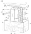
실시예에 따른 지능형 조립전사 통합장치는 반도체 발광소자(150)들을 수용하는 유체 챔버(300)와, 상기 반도체 발광소자(150)가 조립되는 조립 기판(210)이 장착되어 회전되는 롤러부(200) 및 상기 조립 기판(210)에 조립된 상기 반도체 발광소자(150)를 검사하는 조립 검사부(500)를 포함할 수 있다.An intelligent assembly transfer integrated device according to an embodiment may include a fluid chamber (300) that accommodates semiconductor light-emitting elements (150), a roller unit (200) on which an assembly substrate (210) on which the semiconductor light-emitting elements (150) are assembled is mounted and rotated, and an assembly inspection unit (500) that inspects the semiconductor light-emitting elements (150) assembled on the assembly substrate (210).
상기 롤러부(200)는, 상기 조립 기판(210)이 장착되고 회전되는 롤러 회전부(220)와, 상기 롤러 회전부(220)를 회전구동시키는 롤러 구동부(230) 및 상기 반도체 발광소자(150)에 자력을 가하여 상기 조립 기판(210)에 조립되도록 하는 자석헤드부(400)를 포함할 수 있다.The above roller part (200) may include a roller rotation part (220) on which the assembly board (210) is mounted and rotated, a roller driving part (230) that rotates the roller rotation part (220), and a magnet head part (400) that applies a magnetic force to the semiconductor light-emitting element (150) to assemble it to the assembly board (210).
상기 조립 검사부(500)는 상기 조립 기판(210)의 폭 방향으로 라인별 조립 상태를 검사하여 미조립이나 불량조립이 있는 경우의 패널 기판(910)으로 전사공정이 진행되지 않도록 제어할 수 있다.The above assembly inspection unit (500) can inspect the assembly status of each line in the width direction of the assembly board (210) and control the transfer process not to proceed to the panel board (910) in case of non-assembly or defective assembly.
상기 조립 기판(210)의 폭 방향으로 라인별 조립 상태를 검사하여 미조립이나 불량 조립의 에러위치(E)가 있는 경우 소정의 패널 척이 상기 패널 기판(110)을 이동하여 상기 조립 기판(210)과 상기 패널기판(910)을 이격시킴으로써 에러위치의 반도체 발광소자(150)가 상기 패널기판(910)으로 전사되지 않도록 제어할 수 있다.When the assembly status of each line in the width direction of the above assembly board (210) is inspected and an error location (E) of non-assembly or defective assembly is found, a predetermined panel chuck moves the panel board (110) to separate the assembly board (210) and the panel board (910), thereby controlling the semiconductor light-emitting element (150) of the error location from being transferred to the panel board (910).
상기 패널 척은 상기 패널 기판(910)의 측면, 상면 또는 저면에 배치되어 상기 패널 기판(910)을 상기 조립 기판(210)과 이격시킬 수 있다.The above panel chuck can be placed on the side, top or bottom surface of the panel substrate (910) to separate the panel substrate (910) from the assembly substrate (210).
상기 자석 헤드부(400)는 회전 또는 수평 이동함으로써 상기 반도체 발광소자(150)에 자력을 고르게 가할 수 있다.The above magnetic head part (400) can evenly apply magnetic force to the semiconductor light-emitting element (150) by rotating or moving horizontally.
상기 패널 척은 상기 제2패널 기판(912)이 기울어진 상태에서 이동되도록 상기 패널 기판(110)의 회전기능을 가질 수 있다.The above panel chuck may have a rotation function of the panel substrate (110) so that the second panel substrate (912) moves in an inclined state.
상기 패널 기판(910)을 이동하도록 구동하는 패널 구동부를 더 포함할 수 있다.It may further include a panel driving unit that drives the above panel substrate (910) to move.
상기 패널 구동부(920B)는, 제2-1패널 구동부(920b1)와 제2-2패널 구동부(920b2)를 포함하되, 상기 제2-1패널 구동부(920b1)가 상기 제2-2패널 구동부(920b2)와 서로 다른 높이에 배치될 수 있다.The above panel driving unit (920B) includes a 2-1 panel driving unit (920b1) and a 2-2 panel driving unit (920b2), but the 2-1 panel driving unit (920b1) can be positioned at a different height from the 2-2 panel driving unit (920b2).
상기 롤러부는 삼각형 형태 또는 라운드 형태를 포함할 수 있다.The above roller portion may have a triangular shape or a round shape.
상기 반도체 발광소자(150)와 상기 조립 기판(210)간의 조립되는 제1-1 롤러부의 면적이 상기 반도체 발광소자(150)가 상기 패널 기판(910)으로 전사되는 제1-2 롤러부의 면적보다 넓을 수 있다.The area of the 1-1 roller portion assembled between the semiconductor light-emitting element (150) and the assembly substrate (210) may be wider than the area of the 1-2 roller portion through which the semiconductor light-emitting element (150) is transferred to the panel substrate (910).
상기 유체 챔버(300) 하측에 배치되는 제2 자석 헤드부(420)를 더 포함할 수 있다.It may further include a second magnetic head portion (420) positioned at the lower side of the fluid chamber (300).
실시예에 따른 반도체 발광소자의 지능형 조립전사 통합장치에 의하면, 디스플레이 패널에 반도체 발광소자들을 전사함에 있어서 전사속도와 전사수율을 동시에 향상시킬 수 있는 기술적 효과가 있다.According to the intelligent assembly transfer integrated device of a semiconductor light-emitting device according to an embodiment, there is a technical effect of simultaneously improving the transfer speed and transfer yield when transferring semiconductor light-emitting devices onto a display panel.
실시예에 의하면 반도체 발광소자(150)가 전사 기판(transfer substrate)(210)에 조립되고, 조립된 반도체 발광소자(150)들이 인 라인으로 패널 기판(panel substrate)(110)으로 즉시 전사됨으로써 전사 속도를 현저히 향상시킬 수 있다. 또한 실시예에 의하면 전사 기판(210)에 조립된 반도체 발광소자(150)들에 대해 실시간으로 검사를 진행 후 정상인 경우에만 선택적으로 패널 기판(910)에 전사를 진행함으로써 전사 수율을 현저히 높일 수 있다. 이에 따라 실시예에 의하면 전사 속도를 높임과 동시에 전사 수율을 동시에 높임으로써 전사 속도와 전사 수율 간의 기술적 모순이 발생하는 문제를 해결할 수 있는 특별한 기술적 효과가 있다.According to an embodiment, a semiconductor light emitting device (150) is assembled on a transfer substrate (210), and the assembled semiconductor light emitting devices (150) are immediately transferred in-line to a panel substrate (110), whereby the transfer speed can be significantly improved. In addition, according to an embodiment, the semiconductor light emitting devices (150) assembled on the transfer substrate (210) are inspected in real time, and only when they are normal are selectively transferred to the panel substrate (910), whereby the transfer yield can be significantly improved. Accordingly, according to an embodiment, there is a special technical effect of being able to solve the problem of a technical contradiction between the transfer speed and the transfer yield by simultaneously increasing the transfer speed and the transfer yield.
구체적으로 실시예에 의하면 롤러부(200) 상의 조립 기판(210)과 평평한 패널 기판(910)이 만나는 부분은 롤러부(200)의 폭 방향으로 라인(line) 전사를 할 수 있다. 또한 실시예에 의하면 조립 검사를 통해 선별된 불량 없는 완전 조립된 라인 상의 반도체 발광소자만 전사하기 때문에 100% 전사 수율의 구현이 가능하다.Specifically, according to the embodiment, the part where the assembly substrate (210) and the flat panel substrate (910) on the roller section (200) meet can be subjected to line transfer in the width direction of the roller section (200). In addition, according to the embodiment, since only the semiconductor light-emitting elements on the fully assembled line without defects selected through assembly inspection are transferred, it is possible to implement a 100% transfer yield.
이에 따라 실시예에 의하면 조립기판 불량이나 반도체 발광소자의 불량이 있더라도 이를 피해 전사할 수 있어 반도체 발광소자의 품질에 대한 의존성을 최소화할 수 있다.Accordingly, according to the embodiment, even if there is a defect in the assembly board or a defect in the semiconductor light-emitting device, it is possible to avoid these and transfer them, thereby minimizing dependence on the quality of the semiconductor light-emitting device.
또한 실시예에 의하면 조립공정과 전사공정을 분리하되 인라인으로 연결하였기 때문에 조립 시스템의 크기에 따른 전사 면적의 제한이 없는 효과가 있다.In addition, according to the embodiment, since the assembly process and the transfer process are separated but connected inline, there is an effect of no limitation on the transfer area according to the size of the assembly system.
또한 실시예에 의하면 패널 기판의 에지부분에 조립을 위한 별도 공간이 필요하지 않기 때문에 대면적 공정 후 소면적으로 면취할 때 높은 면취율의 확보가 가능한 효과가 있다.In addition, according to the embodiment, since a separate space for assembly is not required at the edge of the panel substrate, there is an effect of ensuring a high chamfering rate when chamfering a small area after a large-area process.
또한 실시예에 의하면 롤러부를 멀티로 구성하면 고속 전사 구현이 가능한 효과가 있다.In addition, according to an embodiment, if the roller section is configured in multiple configurations, it has the effect of enabling high-speed transfer implementation.
실시예의 기술적 효과는 본 항목에 기재된 것에 한정되는 것이 아니며, 발명의 설명을 통해 파악될 수 있는 것을 포함한다.The technical effects of the embodiments are not limited to those described in this article, but include those that can be understood through the description of the invention.
도 1은 실시예에 따른 디스플레이 장치(100)가 세탁기(10), 로봇 청소기(20), 공기청정기(30) 등과 함께 거실에 배치된 예시도.
도 2a는 도 1에서 A1 영역의 확대도.
도 2b는 도 2a에서 A2 영역의 확대도.
도 2c는 도 2b에서 반도체 발광소자(150)의 단면도.
도 3은 실시예에 따른 지능형 조립전사 통합장치(1000)의 개념도.
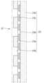
도 4는 도 3에 도시된 실시예에 따른 지능형 조립전사 통합장치(1000)에서 조립기판(210)의 B1 영역의 확대도.
도 5a와 도 5b는 도 3에 도시된 실시예에 따른 지능형 조립전사 통합장치(1000)에서 자석헤드부(400)의 사시도.
도 6은 실시예에 따른 지능형 조립전사 통합장치(1000)의 작동 예시도.
도 7은 실시예에서 패널 기판(110)의 틸팅 개념도.
도 8a 내지 도 8c는 제2 실시예에 따른 지능형 조립전사 통합장치(1000)의 개념도.
도 9는 제3 실시예에 따른 지능형 조립전사 통합장치(1003)의 개념도이다.FIG. 1 is an example diagram showing a display device (100) according to an embodiment of the present invention placed in a living room together with a washing machine (10), a robot vacuum cleaner (20), an air purifier (30), etc.
Figure 2a is an enlarged view of area A1 in Figure 1.
Figure 2b is an enlarged view of area A2 in Figure 2a.
Figure 2c is a cross-sectional view of the semiconductor light emitting element (150) in Figure 2b.
Figure 3 is a conceptual diagram of an intelligent assembly transfer integration device (1000) according to an embodiment.
FIG. 4 is an enlarged view of the B1 area of the assembly board (210) in the intelligent assembly transfer integrated device (1000) according to the embodiment illustrated in FIG. 3.
FIGS. 5A and 5B are perspective views of the magnetic head portion (400) in the intelligent assembly transfer integrated device (1000) according to the embodiment illustrated in FIG. 3.
Figure 6 is an example of the operation of an intelligent assembly transfer integration device (1000) according to an embodiment.
Figure 7 is a conceptual diagram of tilting of a panel substrate (110) in an embodiment.
Figures 8a to 8c are conceptual diagrams of an intelligent assembly transfer integration device (1000) according to the second embodiment.
Figure 9 is a conceptual diagram of an intelligent assembly transfer integration device (1003) according to the third embodiment.
이하, 첨부된 도면을 참조하여 본 명세서에 개시된 실시예를 상세히 설명하되, 도면 부호에 관계없이 동일하거나 유사한 구성요소는 동일한 참조 번호를 부여하고 이에 대한 중복되는 설명은 생략하기로 한다. 이하의 설명에서 사용되는 구성요소에 대한 접미사 '모듈' 및 '부'는 명세서 작성의 용이함이 고려되어 부여되거나 혼용되는 것으로서, 그 자체로 서로 구별되는 의미 또는 역할을 갖는 것은 아니다. 또한, 첨부된 도면은 본 명세서에 개시된 실시예를 쉽게 이해할 수 있도록 하기 위한 것이며, 첨부된 도면에 의해 본 명세서에 개시된 기술적 사상이 제한되는 것은 아니다. 또한, 층, 영역 또는 기판과 같은 요소가 다른 구성요소 '상(on)'에 존재하는 것으로 언급될 때, 이것은 직접적으로 다른 요소 상에 존재하거나 또는 그 사이에 다른 중간 요소가 존재할 수도 있는 것을 포함한다.Hereinafter, embodiments disclosed in the present specification will be described in detail with reference to the attached drawings. Regardless of the drawing symbols, identical or similar components will be given the same reference numerals and redundant descriptions thereof will be omitted. The suffixes 'module' and 'part' for components used in the following description are assigned or used interchangeably in consideration of the ease of writing the specification, and do not in themselves have distinct meanings or roles. In addition, the attached drawings are intended to facilitate easy understanding of the embodiments disclosed in the present specification, and the technical ideas disclosed in the present specification are not limited by the attached drawings. In addition, when an element such as a layer, region, or substrate is mentioned as existing 'on' another element, this includes that it may be directly on the other element or that other intermediate elements may exist therebetween.
본 명세서에서 설명되는 디스플레이 장치에는 휴대폰, 스마트 폰(smart phone), 노트북 컴퓨터(laptop computer), 디지털방송용 단말기, PDA(personal digital assistants), PMP(portable multimedia player), 네비게이션, 슬레이트(Slate) PC, 태블릿(Tablet) PC, 울트라 북(Ultra-Book), 디지털 TV, 데스크탑 컴퓨터 등이 포함될 수 있다. 그러나, 본 명세서에 기재된 실시예에 따른 구성은 추후 개발되는 새로운 제품형태이라도, 디스플레이가 가능한 장치에도 적용될 수 있다.The display devices described in this specification may include mobile phones, smart phones, laptop computers, digital broadcasting terminals, personal digital assistants (PDAs), portable multimedia players (PMPs), navigation devices, slate PCs, tablet PCs, Ultra-Books, digital TVs, desktop computers, and the like. However, the configuration according to the embodiments described in this specification may also be applied to devices capable of displaying, even if they are new product types developed in the future.
(제1 실시예)(Example 1)
실시예에 따른 반도체 발광소자의 지능형 조립전사 통합장치를 설명하기에 앞서, 실시예에서 적용되는 반도체 발광소자 및 이를 이용한 디스플레이 장치에 대해 설명한다(이하 '제1 실시예'는 '실시예'라 칭한다).Before describing an intelligent assembly transfer integrated device for a semiconductor light-emitting device according to an embodiment, a semiconductor light-emitting device applied in the embodiment and a display device using the same are described (hereinafter, 'the first embodiment' is referred to as 'the embodiment').
도 1은 실시예에 따른 디스플레이 장치(100)가 세탁기(10), 로봇 청소기(20), 공기청정기(30) 등과 함께 거실에 배치된 예시도이다.FIG. 1 is an example diagram showing a display device (100) according to an embodiment of the present invention placed in a living room together with a washing machine (10), a robot vacuum cleaner (20), an air purifier (30), etc.
실시예의 디스플레이 장치(100)는 공기청정기(30), 로봇 청소기(20), 세탁기(10) 등의 각종 전자제품의 상태를 표시할 수 있고, 각 전자 제품들과 IOT 기반으로 통신할 수 있으며 사용자의 설정 데이터에 기초하여 각 전자 제품들을 제어할 수도 있다.The display device (100) of the embodiment can display the status of various electronic products such as an air purifier (30), a robot vacuum cleaner (20), a washing machine (10), etc., and can communicate with each electronic product based on IoT and control each electronic product based on the user's setting data.
실시예에 따른 디스플레이 장치(100)는 얇고 유연한 기판 위에 제작되는 플렉서블 디스플레이(flexible display)를 포함할 수 있다. 상기 플렉서블 디스플레이는 기존의 평판 디스플레이의 특성을 유지하면서, 종이와 같이 휘어지거나 말릴 수 있다.A display device (100) according to an embodiment may include a flexible display manufactured on a thin and flexible substrate. The flexible display may be bent or rolled like paper while maintaining the characteristics of a conventional flat panel display.
상기 플렉서블 디스플레이에서 시각정보는 매트릭스 형태로 배치되는 단위 화소(unit pixel)의 발광이 독자적으로 제어됨에 의하여 구현될 수 있다. 상기 단위 화소는 하나의 색을 구현하기 위한 최소 단위를 의미한다. 상기 플렉서블 디스플레이의 단위 화소는 반도체 발광소자(semiconductor light emitting device)에 의하여 구현될 수 있다. 실시예에서 반도체 발광소자는 Micro-LED일 수 있다.In the flexible display, visual information can be implemented by independently controlling the light emission of unit pixels arranged in a matrix form. The unit pixel means the minimum unit for implementing one color. The unit pixel of the flexible display can be implemented by a semiconductor light emitting device. In an embodiment, the semiconductor light emitting device can be a Micro-LED.
다음으로 도 2a는 도 1에서 A1 영역의 확대도이고, 도 2b는 도 2a에서 A2 영역의 확대도이고, 도 2c는 도 2b에서 반도체 발광소자(150)의 단면도이다.Next, FIG. 2a is an enlarged view of area A1 in FIG. 1, FIG. 2b is an enlarged view of area A2 in FIG. 2a, and FIG. 2c is a cross-sectional view of a semiconductor light-emitting element (150) in FIG. 2b.
도 2a에 의하면, 실시예의 디스플레이 장치(100)는 액티브 매트릭스(AM, Active Matrix)방식 또는 패시브 매트릭스(PM, Passive Matrix) 방식으로 반도체 발광소자를 구동할 수 있다.According to FIG. 2a, the display device (100) of the embodiment can drive a semiconductor light-emitting element in an active matrix (AM) method or a passive matrix (PM) method.
다음으로 도 2b를 참조하면, 실시예의 디스플레이 장치(100)는 패널 기판(910), 제1 패널 전극(120), 제2 패널 전극(미도시), 절연층(130) 및 복수의 반도체 발광소자(150)를 포함할 수 있다.Next, referring to FIG. 2b, the display device (100) of the embodiment may include a panel substrate (910), a first panel electrode (120), a second panel electrode (not shown), an insulating layer (130), and a plurality of semiconductor light-emitting elements (150).
각각의 반도체 발광소자(150)는 각각 단위 화소(sub-pixel)를 이루기 위하여 적색, 녹색 및 청색 반도체 발광소자를 포함할 수 있으나 이에 한정되는 것은 아니며, 적색 형광체와 녹색 형광체 등을 구비하여 각각 적색과 녹색을 구현할 수도 있다.Each semiconductor light-emitting element (150) may include red, green, and blue semiconductor light-emitting elements to form a unit pixel (sub-pixel), but is not limited thereto, and may include a red fluorescent substance and a green fluorescent substance to implement red and green, respectively.
상기 패널 기판(910)은 유리나 폴리이미드(Polyimide)로 형성될 수 있다. 또한 상기 패널 기판(910)은 PEN(Polyethylene Naphthalate), PET(Polyethylene Terephthalate) 등의 유연성 있는 재질을 포함할 수 있다. 또한, 상기 패널 기판(910)은 투명한 재질일 수 있으나 이에 한정되는 것은 아니다.The above panel substrate (910) may be formed of glass or polyimide. In addition, the panel substrate (910) may include a flexible material such as PEN (Polyethylene Naphthalate) or PET (Polyethylene Terephthalate). In addition, the panel substrate (910) may be a transparent material, but is not limited thereto.
상기 절연층(130)은 폴리이미드, PEN, PET 등과 같이 절연성과 유연성 있는 재질을 포함할 수 있으며, 상기 패널 기판(910)과 일체로 이루어져 하나의 기판을 형성할 수도 있다.The above insulating layer (130) may include an insulating and flexible material such as polyimide, PEN, PET, etc., and may be formed integrally with the panel substrate (910) to form a single substrate.
상기 절연층(130)은 접착성과 전도성을 가지는 전도성 접착층일 수 있고, 전도성 접착층은 연성을 가져서 디스플레이 장치의 플렉서블 기능을 가능하게 할 수 있다. 예를 들어, 상기 절연층(130)은 이방성 전도성 필름(ACF, anisotropy conductive film)이거나 이방성 전도매질, 전도성 입자를 함유한 솔루션(solution) 등의 전도성 접착층일 수 있다. 상기 전도성 접착층은 두께에 대해 수직방향으로는 전기적으로 전도성이나, 두께에 대해 수평방향으로는 전기적으로 절연성을 가지는 레이어일 수 있다.The above insulating layer (130) may be a conductive adhesive layer having adhesiveness and conductivity, and the conductive adhesive layer may have flexibility to enable a flexible function of the display device. For example, the insulating layer (130) may be a conductive adhesive layer such as an anisotropic conductive film (ACF) or an anisotropic conductive medium, a solution containing conductive particles, etc. The conductive adhesive layer may be a layer that is electrically conductive in a direction vertical to the thickness, but electrically insulating in a direction horizontal to the thickness.
다음으로 도 2c를 참조하면, 실시예의 디스플레이 장치(100)에 적용되는 반도체 발광소자(150)의 예시로서 수직형 반도체 발광소자(vertical type semiconductor light emitting device)의 단면도이다. 실시예에서 채용될 수 있는 반도체 발광소자는 수직형 반도체 발광소자에 한정되는 것은 아니며, 수평형 발광소자(lateral type semiconductor light emitting device) 또는 플립형 발광소자를 포함할 수 있다.Next, referring to FIG. 2c, a cross-sectional view of a vertical type semiconductor light emitting device is provided as an example of a semiconductor light emitting device (150) applied to a display device (100) of the embodiment. The semiconductor light emitting device that may be employed in the embodiment is not limited to a vertical type semiconductor light emitting device, and may include a lateral type semiconductor light emitting device or a flip type light emitting device.
실시예에서 채용되는 반도체 발광소자는 전기에너지가 빛 에너지로 변환되는 p-n 접합 다이오드로서 주기율표 상의 Ⅲ족과 Ⅴ족의 원소를 포함하는 화합물 반도체로 제조될 수 있고, 화합물 반도체의 조성비를 조절하여 밴드 갭 에너지를 제어함으로써 적색, 녹색 및 청색 등의 다양한 색상구현이 가능하다.The semiconductor light-emitting device employed in the embodiment is a p-n junction diode in which electrical energy is converted into light energy, and can be manufactured using a compound semiconductor including elements of groups III and V in the periodic table. By controlling the composition ratio of the compound semiconductor and controlling the band gap energy, it is possible to implement various colors such as red, green, and blue.
도 2c를 참조하면, 실시예의 반도체 발광소자(150)는 발광구조물(light emitting structure)(151), 제1전극(152a) 및 제2전극(152b)을 포함할 수 있다. 상기 발광구조물(151)은 제1도전형 반도체층(151a), 활성층(151b) 및 제2도전형 반도체층(151c)을 포함할 수 있다. 상기 제1전극(152a) 또는 상기 제2전극(152b) 상에 패드전극(미도시)이 더 형성될 수 있으나 이에 한정되는 것은 아니다.Referring to FIG. 2c, the semiconductor light emitting device (150) of the embodiment may include a light emitting structure (151), a first electrode (152a), and a second electrode (152b). The light emitting structure (151) may include a first conductive semiconductor layer (151a), an active layer (151b), and a second conductive semiconductor layer (151c). A pad electrode (not shown) may be further formed on the first electrode (152a) or the second electrode (152b), but is not limited thereto.
상기 제1전극(152a) 또는 제2전극(152b) 중 적어도 하나는 자성체층(미도시)을 포함할 수 있다. 상기 제1도전형은 n형이고, 제2도전형은 p형일 수 있으나 이에 한정되는 것은 아니다. 상기 자성체층은 Ni, SmCo(samarium-cobalt), Gd 계, La계 및 Mn계 중 적어도 하나의 물질을 포함할 수 있다. 상기 자성체층은 메쉬형태로 배치되거나 도트 형태로 배치되어 광투광성이 우수할 수 있다.At least one of the first electrode (152a) or the second electrode (152b) may include a magnetic layer (not shown). The first conductive type may be n-type, and the second conductive type may be p-type, but is not limited thereto. The magnetic layer may include at least one material from among Ni, SmCo (samarium-cobalt), Gd-based, La-based, and Mn-based. The magnetic layer may be arranged in a mesh shape or in a dot shape to have excellent light transmittance.
실시예의 기술적 과제 중의 하나는 디스플레이 패널에 반도체 발광소자들을 전사함에 있어서 전사속도와 전사수율을 동시에 향상시킬 수 있는 반도체 발광소자의 지능형 조립전사 통합장치를 제공하고자 함이다.One of the technical challenges of the present invention is to provide an intelligent assembly and transfer integrated device for semiconductor light-emitting devices that can simultaneously improve transfer speed and transfer yield when transferring semiconductor light-emitting devices onto a display panel.
도 3은 실시예에 따른 지능형 조립전사 통합장치(1000)의 개념도이다. 도 4는 도 3에 도시된 실시예에 따른 지능형 조립전사 통합장치(1000)에서 조립 기판(210)의 B1 영역의 확대도이며, 도 5a와 도 5b는 도 3에 도시된 실시예에 따른 지능형 조립전사 통합장치(1000)에서 자석헤드부(400)의 사시도이다. 도 6은 실시예에 따른 지능형 조립전사 통합장치(1000)의 작동 예시도이다.FIG. 3 is a conceptual diagram of an intelligent assembly transfer integrated device (1000) according to an embodiment. FIG. 4 is an enlarged view of an area B1 of an assembly board (210) in an intelligent assembly transfer integrated device (1000) according to an embodiment illustrated in FIG. 3, and FIGS. 5a and 5b are perspective views of a magnetic head portion (400) in an intelligent assembly transfer integrated device (1000) according to an embodiment illustrated in FIG. 3. FIG. 6 is an exemplary operation diagram of an intelligent assembly transfer integrated device (1000) according to an embodiment.
또한 실시예에 따른 지능형 조립전사 통합장치(1000)는 친수처리 유닛(600), 세정 유닛(700), 건조 유닛(800) 등을 포함할 수 있다.In addition, the intelligent assembly transfer integrated device (1000) according to the embodiment may include a hydrophilic treatment unit (600), a cleaning unit (700), a drying unit (800), etc.
또한 실시예에 따른 지능형 조립전사 통합장치(1000)는 디스플레이 패널 기판(910)을 수평 이동시키는 패널 구동부(920)와 패널 기판(910)을 상하 이동시키는 패널 척(미도시)을 포함할 수 있다.In addition, the intelligent assembly transfer integrated device (1000) according to the embodiment may include a panel driving unit (920) that moves the display panel substrate (910) horizontally and a panel chuck (not shown) that moves the panel substrate (910) up and down.
실시예에 의하면 반도체 발광소자(150)가 전사 기판(transfer substrate)(210)에 조립되고, 조립된 반도체 발광소자(150)들이 인 라인으로 패널 기판(panel substrate)(110)으로 즉시 전사됨으로써 전사 속도를 현저히 향상시킬 수 있다. 또한 실시예에 의하면 전사 기판(210)에 조립된 반도체 발광소자(150)들에 대해 실시간으로 검사를 진행 후 정상인 경우에만 선택적으로 패널 기판(910)에 전사를 진행함으로써 전사 수율을 현저히 높일 수 있다. 이에 따라 실시예에 의하면 전사 속도를 높임과 동시에 전사 수율을 동시에 높임으로써 전사 속도와 전사 수율 간의 기술적 모순이 발생하는 문제를 해결할 수 있는 특별한 기술적 효과가 있다.According to an embodiment, a semiconductor light emitting device (150) is assembled on a transfer substrate (210), and the assembled semiconductor light emitting devices (150) are immediately transferred in-line to a panel substrate (110), whereby the transfer speed can be significantly improved. In addition, according to an embodiment, the semiconductor light emitting devices (150) assembled on the transfer substrate (210) are inspected in real time, and only when they are normal are selectively transferred to the panel substrate (910), whereby the transfer yield can be significantly improved. Accordingly, according to an embodiment, there is a special technical effect of being able to solve the problem of a technical contradiction between the transfer speed and the transfer yield by simultaneously increasing the transfer speed and the transfer yield.
이하 도 3 내지 도 6을 참조하여 실시예에 따른 지능형 조립전사 통합장치(1000)를 상세히 설명하기로 한다.Hereinafter, an intelligent assembly transfer integration device (1000) according to an embodiment will be described in detail with reference to FIGS. 3 to 6.
<유체 챔버, 친수처리 유닛><Fluid chamber, hydrophilic treatment unit>
도 3을 참조하면, 실시예에 따른 지능형 조립전사 통합장치(1000)는 복수의 반도체 발광소자(150)들을 수용하는 유체 챔버(300), 친수처리 유닛(600) 등을 포함할 수 있다.Referring to FIG. 3, the intelligent assembly transfer integrated device (1000) according to the embodiment may include a fluid chamber (300) that accommodates a plurality of semiconductor light-emitting elements (150), a hydrophilic treatment unit (600), etc.
상기 유체 챔버(300)는 수조일 수 있으며, 오픈형 또는 클로즈형일 수 있다. 상기 유체 챔버(300)에는 초순수(deionized water) 등의 조립용액이 채워질 수 있으나 이에 한정되는 것은 아니다.The above fluid chamber (300) may be a water tank and may be open or closed. The fluid chamber (300) may be filled with an assembly solution such as deionized water, but is not limited thereto.
상기 친수처리 유닛(600)은 조립 기판(210)이 유체에 입수하기 전에 웨팅(wetting)을 위한 친수 처리를 할 수 있다.The above hydrophilic treatment unit (600) can perform hydrophilic treatment for wetting before the assembly substrate (210) is immersed in a fluid.
<조립 기판><Assembly board>
실시예는 롤러부(200)에 장착되는 유연성 조립 기판(210)을 포함할 수 있다. 상기 조립 기판(210)은 캐리어 기판, 제1 전사 기판으로 칭해질 수 있다.The embodiment may include a flexible assembly substrate (210) mounted on a roller portion (200). The assembly substrate (210) may be referred to as a carrier substrate, a first transfer substrate.
예를 들어, 조립 기판(210)은 롤러 회전부(220)에 장착될 수 있는 유연성 기판일 수 있다. 예를 들어, 조립 기판(210)은 롤(roll)처럼 말수 있는 유연성 재질일 수 있으며, 폴리이미드(Polyimide) 등의 폴리머나 얇은 메탈 기판(metal substrate) 등일 수 있으나 이에 한정되는 것은 아니다.For example, the assembly substrate (210) may be a flexible substrate that can be mounted on the roller rotation part (220). For example, the assembly substrate (210) may be a flexible material that can be rolled like a roll, and may be a polymer such as polyimide or a thin metal substrate, but is not limited thereto.
도 4는 도 3에 도시된 실시예에 따른 지능형 조립전사 통합장치(1000)에서 조립 기판(210)의 B1 영역의 확대도이다.FIG. 4 is an enlarged view of the B1 area of the assembly board (210) in the intelligent assembly transfer integration device (1000) according to the embodiment illustrated in FIG. 3.
상기 조립 기판(210)은 베이스부(210a), 유전체층(210b) 및 복수의 조립전극(210c)을 포함하여 전기장 형성이 가능할 수 있다.The above assembly substrate (210) may be capable of forming an electric field by including a base portion (210a), a dielectric layer (210b), and a plurality of assembly electrodes (210c).
상기 베이스부(210a)는 절연성 있는 재질로 이루어지며, 상기 복수의 조립전극(210c)은 상기 베이스부(210a)의 일면에 패턴된 박막 또는 후막의 bi-planar 전극이 될 수 있다. 상기 조립전극(210c)은 Ti/Cu/Ti의 적층, Ag 페이스트 및 ITO 등으로 형성될 수 있다.The above base portion (210a) is made of an insulating material, and the plurality of assembly electrodes (210c) can be bi-planar electrodes of a thin film or thick film patterned on one surface of the base portion (210a). The assembly electrodes (210c) can be formed of a laminate of Ti/Cu/Ti, Ag paste, ITO, etc.
상기 유전체층(210b)은 SiO2, SiNx, SiON, Al2O3, TiO2, HfO2 등의 무기 물질로 이루어질 있다. 또한 상기 유전체층(210b)은 유기 절연체로서 단일층이거나 멀티층으로 형성될 수 있다.The above dielectric layer (210b) may be made of an inorganic material such as SiO2 , SiNx, SiON, Al2 O3 , TiO2 , or HfO2 . In addition, the above dielectric layer (210b) may be formed as a single layer or multi-layer as an organic insulator.
또한 상기 조립 기판(210)은 격벽(210e)에 의하여 구획되는 복수의 셀들(210d)을 포함할 수 있다. 상기 셀들(210d)은 일방향을 따라 순차적으로 배치되며, 폴리머(polymer) 재질로 형성될 수 있다. 또한, 상기 셀들(210d)을 이루는 격벽(210e)은 이웃하는 셀들(210d)과 공유될 수 있다.In addition, the assembly board (210) may include a plurality of cells (210d) partitioned by partition walls (210e). The cells (210d) are arranged sequentially along one direction and may be formed of a polymer material. In addition, the partition walls (210e) forming the cells (210d) may be shared with neighboring cells (210d).
상기 격벽(210e)은 상기 베이스부(210a)에서 상측방향으로 돌출될 수 있으며, 상기 격벽(210e)에 의하여 상기 셀들(210d)이 일방향을 따라 순차적으로 배치될 수 있다. 예를 들어, 상기 셀들(210d)은 열과 행 방향으로 각각 순차적으로 배치되며, 매트릭스 구조일 수 있다.The above-mentioned partition wall (210e) may protrude upward from the above-mentioned base portion (210a), and the cells (210d) may be sequentially arranged along one direction by the above-mentioned partition wall (210e). For example, the cells (210d) may be sequentially arranged in the column and row directions, respectively, and may have a matrix structure.
상기 셀들(210d)의 내부는 반도체 발광소자(150)를 수용하는 조립 홈이 될 수 있으며, 상기 조립 홈은 상기 격벽(210e)에 의하여 구획되는 공간이 될 수 있다.The interior of the above cells (210d) can be an assembly groove that accommodates a semiconductor light-emitting element (150), and the assembly groove can be a space partitioned by the partition wall (210e).
상기 조립 홈의 형상은 반도체 발광소자(150)의 외곽 형상과 동일 또는 유사할 수 있다. 예를 들어, 상기 반도체 발광소자(150)가 사각형상인 경우, 조립 홈은 사각형상일 수 있다. 또한, 상기 반도체 발광소자(150)가 원형인 경우, 상기 조립 홈은 원형일 수 있다. 또한 각각 하나의 셀에는 하나의 반도체 발광소자(150)가 수용될 수 있다.The shape of the above assembly groove may be identical to or similar to the outer shape of the semiconductor light-emitting device (150). For example, if the semiconductor light-emitting device (150) is rectangular, the assembly groove may be rectangular. In addition, if the semiconductor light-emitting device (150) is circular, the assembly groove may be circular. In addition, one semiconductor light-emitting device (150) may be accommodated in each cell.
한편, 복수의 조립전극(210c)은 각각의 셀들(210d)의 바닥에 배치되는 복수의 전극라인을 구비하며, 상기 복수의 전극라인은 이웃한 셀로 연장될 수 있다.Meanwhile, the plurality of assembly electrodes (210c) are provided with a plurality of electrode lines arranged on the bottom of each cell (210d), and the plurality of electrode lines can extend to neighboring cells.
상기 복수의 조립전극(210c)은 상기 셀들(210d)의 하측에 배치되며, 서로 다른 극성이 각각 인가되어 상기 셀들(210d) 내에 전기장을 생성할 수 있다. 상기 전기장 형성을 위하여, 상기 복수의 조립전극(210c)을 유전체층(210b)이 덮으면서, 상기 유전체층(210b)이 셀들(210d)의 바닥을 형성할 수 있다. 각 셀들(210d)의 하측에서 한 쌍의 조립전극(210c)에 전원공급부(미도시)에 의해 서로 다른 극성의 전원이 인가되면 전기장이 형성되고, 상기 전기장에 의하여 상기 셀들(210d) 내부로 상기 반도체 발광소자(150)가 수용되어 조립될 수 있다.The above plurality of assembly electrodes (210c) are arranged on the lower side of the cells (210d), and different polarities can be applied to each of them to generate an electric field within the cells (210d). In order to form the electric field, the plurality of assembly electrodes (210c) can be covered by a dielectric layer (210b), and the dielectric layer (210b) can form the bottom of the cells (210d). When power having different polarities is applied to a pair of assembly electrodes (210c) on the lower side of each of the cells (210d) by a power supply unit (not shown), an electric field is formed, and the semiconductor light-emitting element (150) can be accommodated and assembled within the cells (210d) by the electric field.
<롤러부: 롤러 회전부, 롤러 구동부, 자석 헤드부><Roller section: roller rotation section, roller driving section, magnet head section>
실시예에 따른 지능형 조립전사 통합장치(1000)는 조립 기판(210)을 회전시키는 롤러부(200)를 포함할 수 있다. 상기 롤러부(200)는 롤러 회전부(220), 롤러 구동부(230), 자석 헤드부(400)를 포함할 수 있다.An intelligent assembly transfer integrated device (1000) according to an embodiment may include a roller unit (200) that rotates an assembly substrate (210). The roller unit (200) may include a roller rotation unit (220), a roller driving unit (230), and a magnet head unit (400).
예를 들어, 상기 롤러부(200)는 조립 기판(210)이 장착되고 회전되는 롤러 회전부(220)와, 상기 롤러 회전부(220)가 회전하도록 구동시키는 롤러 구동부(230), 반도체 발광소자(150)에 자력을 가하여 조립 기판(210)에 조립되도록 하는 자석헤드부(400)를 포함할 수 있다.For example, the roller part (200) may include a roller rotation part (220) on which an assembly board (210) is mounted and rotated, a roller driving part (230) that drives the roller rotation part (220) to rotate, and a magnet head part (400) that applies a magnetic force to a semiconductor light-emitting element (150) to assemble it to the assembly board (210).
상기 롤러부(200)는 조립 기판(210)에 조립된 반도체 발광소자(150)들이 패널 기판(910)에 전사될 때 조립 기판(210)과 패널 기판(910)이 한 라인 또는 복수의 라인에서 만나서 반도체 발광소자(150)들이 전사되도록 할 수 있다.The above roller unit (200) can cause the semiconductor light-emitting elements (150) assembled on the assembly substrate (210) to meet the panel substrate (910) in one line or multiple lines so that the semiconductor light-emitting elements (150) are transferred when transferred to the panel substrate (910).
상기 롤러 구동부(230)는 조립 기판(210)이 장착된 롤러 회전부(220)를 롤러 구동부(230)를 이용하여 회전 구동시킬 수 있으며, 상기 롤러 구동부(230)는 단일 또는 복수로 모터를 포함할 수 있으나 이에 한정되는 것은 아니다.The above roller driving unit (230) can drive the roller rotation unit (220) equipped with the assembly board (210) to rotate by using the roller driving unit (230), and the roller driving unit (230) can include a single or multiple motors, but is not limited thereto.
상기 롤러 회전부(220)는 장착된 조립 기판(210)이 효율적으로 회전되도록 유연성 재질로 형성될 수 있다. 또한 상기 롤러 회전부(220)는 벨트 형태로 형태일 수 있으나 이에 한정되는 것은 아니다. 상기 롤러 회전부(220)는 조립 기판(210)이 장착된 상태에서 자석 헤드부(400)의 자력이 반도체 발광소자(150)에 잘 전달될 수 있도록 두께가 5mm이하일 수 있으나 이에 한정되는 것은 아니다.The above roller rotation part (220) may be formed of a flexible material so that the mounted assembly board (210) can rotate efficiently. In addition, the roller rotation part (220) may be in the form of a belt, but is not limited thereto. The roller rotation part (220) may have a thickness of 5 mm or less so that the magnetic force of the magnet head part (400) can be well transmitted to the semiconductor light-emitting element (150) when the assembly board (210) is mounted, but is not limited thereto.
상기 롤러부(200)는 반도체 발광소자(150)가 조립 기판(210)에 부착되도록 자력을 가하는 자석 헤드부(400)를 포함할 수 있다.The above roller part (200) may include a magnet head part (400) that applies a magnetic force so that the semiconductor light-emitting element (150) is attached to the assembly board (210).
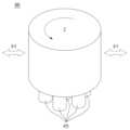
도 5a는 도 3에 도시된 실시예에 따른 지능형 조립전사 통합장치(1000)에서 자석헤드부(400)의 사시도이며, 도 5b는 도 5a에 도시된 자석헤드부(400)의 180도 반전된 사시도이다.FIG. 5a is a perspective view of a magnetic head part (400) in an intelligent assembly transfer integrated device (1000) according to the embodiment illustrated in FIG. 3, and FIG. 5b is a 180-degree inverted perspective view of the magnetic head part (400) illustrated in FIG. 5a.
상기 자석 헤드부(400)는 롤러부(200) 내측에 위치하여 유체 챔버(300) 내의 반도체 발광소자(150)가 조립 기판(210)의 조립 전극(210c) 쪽으로 유도하는 기능을 할 수 있다. 상기 자석 헤드부(400)는 하나 또는 복수일 수 있다.The above magnet head part (400) is positioned inside the roller part (200) and can have the function of guiding the semiconductor light-emitting element (150) in the fluid chamber (300) toward the assembly electrode (210c) of the assembly substrate (210). There may be one or more magnet heads (400).
도 5a를 참조하면, 실시예의 자석 헤드부(400)는 복수의 자석(610)을 구비할 수 있다. 상기 자석(610)은 상기 유체 챔버(300)와 이격 배치되어 상기 반도체 발광소자(150)에 자기력을 가할 수 있고, 상기 자석(610)과 연결되는 위치 제어부(미도시)에 의해 위치가 제어될 수 있다. 상기 자석(610)은 영구 자석이거나 전자석일 수 있다.Referring to FIG. 5a, the magnet head part (400) of the embodiment may be provided with a plurality of magnets (610). The magnets (610) may be spaced apart from the fluid chamber (300) to apply a magnetic force to the semiconductor light-emitting element (150), and their positions may be controlled by a position control part (not shown) connected to the magnets (610). The magnets (610) may be permanent magnets or electromagnets.
실시예는 상기 자석 헤드부(400)를 자동 또는 수동으로 움직일 수 있는 자석 핸 들러(미도시)를 구비하거나, 상기 자석 헤드부(400)를 회전시킬 수 있는 모터(미도시)를 구비하여 자석 헤드부(400)를 시계방향 또는 반시계방향으로 회전구동(Z)할 수 있으며, 조립 기판(210)의 회전방향과 수직방향으로 자석 헤드부(400)를 수평구동(X-Y)할 수 있다.The embodiment comprises a magnetic handler (not shown) that can automatically or manually move the magnetic head part (400), or a motor (not shown) that can rotate the magnetic head part (400), so that the magnetic head part (400) can be rotated (Z) clockwise or counterclockwise, and the magnetic head part (400) can be horizontally driven (X-Y) in a direction perpendicular to the rotational direction of the assembly board (210).
실시예에서 상기 자석 헤드부(400)는 회전함으로써 반도체 발광소자(150)에 가해지는 자력을 고르게 분산시켜서 조립 속도를 향상시킬 수 있다.In an embodiment, the magnetic head part (400) can evenly distribute the magnetic force applied to the semiconductor light-emitting element (150) by rotating, thereby improving the assembly speed.
또한 상기 자석 헤드부(400)는 상기 조립 기판(210)의 회전방향에 수직방향으로 일정구간을 움직이면서 회전함에 따라 자력을 더욱 고르게 분산시켜서 반도체 발광소자(150)의 조립 속도를 향상시킴과 동시에 조립 기판(210)에 고르게 조립되도록 할 수 있다.In addition, the magnetic head part (400) rotates while moving a certain distance in a direction perpendicular to the rotational direction of the assembly board (210), thereby distributing the magnetic force more evenly, thereby improving the assembly speed of the semiconductor light-emitting element (150) and enabling it to be evenly assembled on the assembly board (210).
<세정 유닛, 건조 유닛, 조립 검사부, 패널 구동부, 패널 척><Cleaning unit, drying unit, assembly inspection unit, panel driving unit, panel chuck>
다시 도 3을 참조하면, 실시예에 따른 지능형 조립전사 통합장치(1000)는 세정 유닛(700), 건조 유닛(800) 및 조립 검사부(500)를 포함할 수 있다.Referring again to FIG. 3, the intelligent assembly transfer integrated device (1000) according to the embodiment may include a cleaning unit (700), a drying unit (800), and an assembly inspection unit (500).
상기 세정 유닛(700)은 조립 기판(210)의 조립 영역 이외의 영역에 용액을 분사하여 조립 기판(210)의 조립 영역 외에 부착된 반도체 발광소자(150)를 떼어낼 수 있고, 한 번에 라인 전체를 커버할 수 있도록 분사할 수 있다.The above cleaning unit (700) can spray a solution to an area other than the assembly area of the assembly board (210) to remove the semiconductor light emitting element (150) attached outside the assembly area of the assembly board (210), and can spray so as to cover the entire line at one time.
상기 건조 유닛(800)은 반도체 발광소자(150)에 열풍이나 열을 가하여 전사되기 전에 조립용액이 증발되도록 할 수 있다.The above drying unit (800) can apply hot air or heat to the semiconductor light emitting element (150) to evaporate the assembly solution before transfer.
상기 조립 검사부(500)는 상기 조립 기판(210)에 반도체 발광소자(150)가 조립되었는지 여부 또는 정확히 조립되었는지 여부를 검사할 수 있다.The above assembly inspection unit (500) can inspect whether a semiconductor light-emitting element (150) has been assembled on the above assembly board (210) or whether it has been assembled correctly.
상기 조립 검사부(500)는 라인 스캔 조립검사를 진행할 수 있고, 한번에 라인 전체의 커버가 가능할 수 있다. 상기 조립 검사부(500)는 CCD 이미지 센서를 포함할 수 있고, 검사 결과를 제어부(미도시)에 전송할 수 있으며, 검사 결과에 따라 패널 기판(910)으로 전사여부를 결정할 수 있다.The above assembly inspection unit (500) can perform a line scan assembly inspection and can cover the entire line at once. The above assembly inspection unit (500) can include a CCD image sensor, can transmit the inspection results to a control unit (not shown), and can determine whether to transfer to the panel substrate (910) based on the inspection results.
도 6은 실시예에 따른 지능형 조립전사 통합장치(1000)의 작동 예시도이다.Figure 6 is an example of the operation of an intelligent assembly transfer integration device (1000) according to an embodiment.
실시예에 따른 지능형 조립전사 통합장치(1000)는 디스플레이 패널 기판(910)을 수평 이동시키는 패널 구동부(920)와 패널 기판(910)을 상하 이동시키는 패널 척(미도시)을 포함할 수 있다.An intelligent assembly transfer integrated device (1000) according to an embodiment may include a panel driving unit (920) that moves a display panel substrate (910) horizontally and a panel chuck (not shown) that moves the panel substrate (910) up and down.
상기 패널 구동부(920)는 단일 또는 복수로 구비될 수 있으며, 도 6에서는 2개로 도시되어 있으나 이에 한정되는 것은 아니다. 상기 패널 구동부(920)는 모터를 통해 구동될 수 있으나 이에 한정되는 것은 아니다.The above panel driving unit (920) may be provided in single or multiple units, and is illustrated as two units in FIG. 6, but is not limited thereto. The above panel driving unit (920) may be driven by a motor, but is not limited thereto.
상기 패널 척은 상기 패널 기판(910)의 측면, 상면 또는 저면에 배치되어 상기 패널 기판(910)을 상기 조립 기판(210)과 이격시킬 수 있다.The above panel chuck can be placed on the side, top or bottom surface of the panel substrate (910) to separate the panel substrate (910) from the assembly substrate (210).
실시예에 의하면 조립 기판(210)의 폭 방향으로 라인별 조립 상태를 검사하여 미조립이나 불량 조립이 있는 경우의 라인 위치 정보를 시스템 제어부(미도시)에 전달하여 패널 기판(910)에 전사공정이 진행되지 않도록 제어할 수 있다.According to an embodiment, the assembly status of each line in the width direction of the assembly board (210) is inspected, and in the case of non-assembly or defective assembly, line location information is transmitted to the system control unit (not shown) so that the transfer process is not performed on the panel board (910).
예를 들어, 조립 기판(210)의 폭 방향으로 라인별 조립 상태를 검사하여 미조립이나 불량 조립 등 에러위치(E)가 있는 경우의 패널 척을 통해 패널 기판(910)을 상측으로 이동되게 함으로써 조립 기판(210)과 패널기판(910)을 이격시킴으로써 패널 기판(910)에 에러위치 라인 상의 반도체 발광소자(150)가 전사되지 않도록 제어할 수 있는 특별한 기술적 효과가 있다.For example, by inspecting the assembly status of each line in the width direction of the assembly board (210) and moving the panel board (910) upward through the panel chuck in the case where there is an error position (E) such as non-assembly or defective assembly, thereby separating the assembly board (210) and the panel board (910), there is a special technical effect of being able to control the semiconductor light emitting element (150) on the error position line to not be transferred to the panel board (910).
실시예에 의하면 조립 기판(210)에 라인별 픽셀 중에 반도체 발광소자(150)가 조립되지 않거나 제대로 조립되지 않는 경우 해당 라인 상의 반도체 발광소자(150)는 패널 기판(910)에 전사되지 않도록 하여 전사 속도 및 전사 수율을 동시에 높일 수 있는 특별한 기술적 효과가 있다.According to an embodiment, if a semiconductor light-emitting element (150) is not assembled or not properly assembled among pixels per line on an assembly board (210), the semiconductor light-emitting element (150) on the corresponding line is prevented from being transferred to a panel board (910), thereby providing a special technical effect of simultaneously increasing the transfer speed and transfer yield.
도 7은 실시예에서 패널 기판(910)의 틸팅 개념도이다.Figure 7 is a conceptual diagram of tilting of a panel substrate (910) in an embodiment.
실시예에서 패널 척은 조립 기판(210)에서 패널 기판(910)으로 반도체 발광소자(150)가 보다 잘 전사될 수 있도록 패널 기판(910)의 미세 회전기능을 가질 수 있다.In an embodiment, the panel chuck may have a micro-rotation function of the panel substrate (910) so that the semiconductor light emitting element (150) can be better transferred from the assembly substrate (210) to the panel substrate (910).
도 7의 (A)를 참조하면 실시예에서 패널 구동부(920)는 제1-1패널 구동부(920a1)와 제1-2 패널 구동부(920a2)를 포함할 수 있다. 상기 제1-1 패널 구동부(920a1)와 상기 제1-2 패널 구동부(920a2)의 높이는 같을 수 있으며, 이에 따라 패널 기판(910)은 수평을 유지한 상태에서 이동되면서 반도체 발광소자(150)의 전사가 진행될 수 있다.Referring to (A) of FIG. 7, in the embodiment, the panel driving unit (920) may include a 1-1 panel driving unit (920a1) and a 1-2 panel driving unit (920a2). The heights of the 1-1 panel driving unit (920a1) and the 1-2 panel driving unit (920a2) may be the same, and accordingly, the panel substrate (910) may be moved while maintaining a horizontal state, and the transfer of the semiconductor light-emitting element (150) may proceed.
한편, 도 7의 (B)를 참조하면, 실시예에서 제2패널 구동부(920B)는 제2-1패널 구동부(920b1)와 제2-2패널 구동부(920b2)를 포함하되, 상기 제2-1패널 구동부(920b1)가 상기 제2-2패널 구동부(920b2)와 서로 다른 높이에 배치될 수 있다.Meanwhile, referring to (B) of FIG. 7, in the embodiment, the second panel driving unit (920B) includes a second-first panel driving unit (920b1) and a second-second panel driving unit (920b2), but the second-first panel driving unit (920b1) may be arranged at a different height from the second-second panel driving unit (920b2).
예를 들어, 상기 제2-1패널 구동부(920b1)가 상기 제2-2패널 구동부(920b2)보다 낮게 배치될 수 있다. 이에 따라 제2패널 기판(912)의 전단(912b1)은 후단(912b2)에 비해 낮게 배치될 수 있다. 상기 제2패널 기판(912)이 기울어진 상태에서 이동되면서 반도체 발광소자(150)의 전사가 진행될 수 있다. 이에 따라 반도체 발광소자(150)가 상기 조립 기판(210)에서 상기 제2 패널 기판(912)으로 전사가 보다 효과적으로 진행될 수 있다.For example, the 2-1 panel driving unit (920b1) may be positioned lower than the 2-2 panel driving unit (920b2). Accordingly, the front end (912b1) of the 2nd panel substrate (912) may be positioned lower than the rear end (912b2). The transfer of the semiconductor light-emitting element (150) may proceed while the 2nd panel substrate (912) is moved in an inclined state. Accordingly, the semiconductor light-emitting element (150) may be transferred more effectively from the assembly substrate (210) to the 2nd panel substrate (912).
실시예에 따른 반도체 발광소자의 지능형 조립전사 통합장치에 의하면, 디스플레이 패널에 반도체 발광소자들을 전사함에 있어서 전사속도와 전사수율을 동시 향상시킬 수 있는 기술적 효과가 있다.According to the intelligent assembly transfer integrated device of a semiconductor light-emitting device according to an embodiment, there is a technical effect of simultaneously improving the transfer speed and transfer yield when transferring semiconductor light-emitting devices onto a display panel.
구체적으로 실시예에 의하면 롤러부(200) 상의 조립 기판(210)과 평평한 패널 기판(910)이 만나는 부분은 롤러부(200)의 폭 방향으로 라인(line) 전사를 할 수 있다. 또한 실시예에 의하면 조립 검사를 통해 선별된 불량 없는 완전 조립된 라인 상의 반도체 발광소자만 전사하기 때문에 100% 전사 수율의 구현이 가능하다.Specifically, according to the embodiment, the part where the assembly substrate (210) and the flat panel substrate (910) on the roller section (200) meet can be subjected to line transfer in the width direction of the roller section (200). In addition, according to the embodiment, since only the semiconductor light-emitting elements on the fully assembled line without defects selected through assembly inspection are transferred, it is possible to implement a 100% transfer yield.
이에 따라 실시예에 의하면 조립기판 불량이나 반도체 발광소자의 불량이 있더라도 이를 피해 전사할 수 있어 반도체 발광소자의 품질에 대한 의존성을 최소화할 수 있다.Accordingly, according to the embodiment, even if there is a defect in the assembly board or a defect in the semiconductor light-emitting device, it is possible to avoid these and transfer them, thereby minimizing dependence on the quality of the semiconductor light-emitting device.
또한 실시예에 의하면 조립공정과 전사공정을 분리하되 인라인으로 연결하였기 때문에 조립 시스템의 크기에 따른 전사 면적의 제한이 없는 효과가 있다.In addition, according to the embodiment, since the assembly process and the transfer process are separated but connected inline, there is an effect of no limitation on the transfer area according to the size of the assembly system.
또한 실시예에 의하면 패널 기판의 에지부분에 조립을 위한 별도 공간이 필요하지 않기 때문에 대면적 공정 후 소면적으로 면취할 때 높은 면취율의 확보가 가능한 효과가 있다.In addition, according to the embodiment, since a separate space for assembly is not required at the edge of the panel substrate, there is an effect of ensuring a high chamfering rate when chamfering a small area after a large-area process.
또한 실시예에 의하면 롤러부를 멀티로 구성하면 고속 전사 구현이 가능한 효과가 있다.In addition, according to an embodiment, if the roller section is configured in multiple configurations, it has the effect of enabling high-speed transfer implementation.
<조립, 검사, 전사 공정><Assembly, inspection, and transcription processes>
이하 도 3과 도 6을 참조하여 따른 반도체 발광소자의 지능형 조립전사 통합장치(1000)를 이용한 조립, 검사 및 전사 공정을 설명하기로 한다.Hereinafter, with reference to FIGS. 3 and 6, the assembly, inspection, and transfer processes using the intelligent assembly transfer integrated device (1000) of a semiconductor light-emitting device will be described.
우선 반도체 발광소자(150)를 유체 챔버(300)에 투입하고, 조립 기판(210)을 롤러부(200)에 장착한다.First, a semiconductor light-emitting element (150) is placed into a fluid chamber (300), and an assembly substrate (210) is mounted on a roller section (200).
다음으로, 유체 챔버(300) 내에서 상기 반도체 발광소자(150)가 수직방향으로 떠오르도록 반도체 발광소자(150)에 자석 헤드부(400)를 이용하여 자기력을 가한다.Next, a magnetic force is applied to the semiconductor light-emitting element (150) using the magnet head (400) so that the semiconductor light-emitting element (150) floats vertically within the fluid chamber (300).
상기 자석 헤드부(400)가 전자석인 경우 자기력의 크기를 조절하면 상기 조립 기판(210)의 조립면과 반도체 발광소자(150)의 이격거리가 제어될 수 있다. 예를 들어, 상기 반도체 발광소자(150)의 무게, 부력 및 자기력을 이용하여 이격거리를 제어할 수 있다.If the above magnet head part (400) is an electromagnet, the distance between the assembly surface of the assembly board (210) and the semiconductor light-emitting element (150) can be controlled by adjusting the size of the magnetic force. For example, the distance can be controlled by using the weight, buoyancy, and magnetic force of the semiconductor light-emitting element (150).
다음으로, 상기 유체 챔버(300) 내에서 상기 반도체 발광소자(150)가 일방향을 따라 이동하도록 상기 반도체 발광소자(150)에 자기력을 가한다. 예를 들어, 상기 자석 헤드부(400)의 자석을 조립 기판(210)의 회전방향과 수직한 방향으로 이동시키면서 시계방향 또는 반시계방향으로 회전구동할 수 있다.Next, a magnetic force is applied to the semiconductor light-emitting element (150) so that the semiconductor light-emitting element (150) moves in one direction within the fluid chamber (300). For example, the magnet of the magnet head portion (400) can be rotated clockwise or counterclockwise while moving in a direction perpendicular to the rotational direction of the assembly board (210).
다음으로,상기반도체발광소자(150)의 이동과정에서 조립 기판(210)의 조립위치에 안착되도록 상기 반도체 발광소자(150)에 전기장을 가하여 조립위치로 유도하는 단계가 진행된다. 예를 들어, 상기 반도체 발광소자(150)가 상기 조립 기판(210)을 따라 이동하는 도중에 전기장에 의하여 상기 조립 기판(210)과 수직 또는 수평한 방향으로 이동하여 상기 조립 기판(210)의 조립위치에 안착시킬 수 있다.Next, a step of applying an electric field to the semiconductor light-emitting element (150) to guide it to the assembly position of the assembly substrate (210) is performed so that the semiconductor light-emitting element (150) is settled in the assembly position of the assembly substrate (210) during the movement process of the semiconductor light-emitting element (150). For example, while the semiconductor light-emitting element (150) is moving along the assembly substrate (210), it can be moved in a vertical or horizontal direction with respect to the assembly substrate (210) by an electric field so as to be settled in the assembly position of the assembly substrate (210).
예를 들어, 상기 조립 기판(210)의 bi-planar 전극에 전원을 공급하여 전기장을 생성하고, 이를 이용하여 조립위치에서만 조립이 되도록 제어할 수 있다. 즉 선택적으로 생성한 전기장을 이용하여, 반도체 발광소자(150)가 상기 조립 기판(210)의 조립위치에 스스로 조립되도록 한다.For example, power can be supplied to the bi-planar electrode of the assembly substrate (210) to generate an electric field, and this can be used to control assembly so that it occurs only at the assembly position. That is, by using the selectively generated electric field, the semiconductor light-emitting element (150) is self-assembled at the assembly position of the assembly substrate (210).
다음으로 세정 유닛(700)은 조립영역 외의 영역에 용액을 분사하여 조립 기판(210)의 조립영역 외에 부착된 반도체 발광소자(150)를 떼어낼 수 있고, 한 번에 라인 전체를 커버할 수 있도록 용액을 분사할 수 있다.Next, the cleaning unit (700) can spray a solution to an area outside the assembly area to remove the semiconductor light emitting element (150) attached outside the assembly area of the assembly board (210), and can spray the solution so as to cover the entire line at one time.
다음으로 건조 유닛(800)은 조립된 반도체 발광소자(150)에 열풍이나 열을 가하여 전사 전에 조립용액이 증발되도록 할 수 있다.Next, the drying unit (800) can apply hot air or heat to the assembled semiconductor light-emitting element (150) to evaporate the assembly solution before transfer.
다음으로 조립 검사부(500)는 반도체 발광소자(150)의 조립 기판(210)에 조립 여부, 불량 조립여부를 검사할 수 있다. 상기 조립 검사부(500)는 라인 스캔 조립검사를 진행할 수 있고, 한번에 라인 전체 커버가능할 수 있다. 상기 조립 검사부(500)는 CCD 이미지 센서를 포함할 수 있고, 검사 결과를 제어부에 전송할 수 있으며, 검사 결과에 따라 패널 기판(910)으로 전사여부를 결정할 수 있다.Next, the assembly inspection unit (500) can inspect whether the semiconductor light emitting element (150) is assembled on the assembly substrate (210) or whether there is a defect in the assembly. The assembly inspection unit (500) can perform a line scan assembly inspection and can cover the entire line at once. The assembly inspection unit (500) can include a CCD image sensor, can transmit the inspection results to the control unit, and can determine whether to transfer them to the panel substrate (910) based on the inspection results.
다음으로 도 6을 참조하면, 실시예에 따른 지능형 조립전사 통합장치(1000)에 의하면 조립 기판(210)의 폭 방향으로 라인별 조립 상태를 검사하여 미조립이나 불량 조립이 있는 경우의 라인 위치 정보를 시스템 제어부에 전달하여 패널 기판(910)에 전사공정이 진행되지 않도록 제어할 수 있다.Next, referring to FIG. 6, according to the intelligent assembly transfer integrated device (1000) according to the embodiment, the assembly status of each line in the width direction of the assembly board (210) is inspected, and in the case of non-assembly or defective assembly, line location information is transmitted to the system control unit, so that the transfer process can be controlled so that it does not proceed to the panel board (910).
예를 들어, 조립 기판(210)의 폭 방향으로 라인별 조립 상태를 검사하여 미조립이나 불량 조립 등 에러위치(E)가 있는 경우의 패널 척을 통해 패널 기판(910)을 상측으로 이동되게 함으로써 조립 기판(210)과 이격시킴으로써 패널 기판(910)에 전사공정이 진행되지 않도록 제어할 수 있는 특별한 기술적 효과가 있다.For example, there is a special technical effect that can control the panel substrate (910) to not be transferred by moving it upward through the panel chuck when there is an error position (E) such as unassembled or defective assembly by inspecting the assembly status for each line in the width direction of the assembly substrate (210) so that the panel substrate (910) is separated from the assembly substrate (210).
실시예에 의하면 조립 기판(210)에 라인별 픽셀 중에 반도체 발광소자(150)가 조립되지 않거나 제대로 조립되지 않는 경우 해당 라인 상의 반도체 발광소자(150)가 패널 기판(910)에 전사되지 않도록 하여 전사 속도 및 전사 수율을 동시에 높일 수 있는 특별한 기술적 효과가 있다.According to an embodiment, if a semiconductor light-emitting element (150) is not assembled or not properly assembled among pixels per line on an assembly board (210), there is a special technical effect of preventing the semiconductor light-emitting element (150) on the corresponding line from being transferred to the panel board (910), thereby simultaneously increasing the transfer speed and transfer yield.
다시 도 3을 참조하면, 패널 기판(910)으로 전사된 반도체 발광소자(150)에 대해 디스플레이 장치를 구현하기 위한 후공정이 진행될 수 있다.Referring again to FIG. 3, a post-process may be performed to implement a display device for a semiconductor light-emitting element (150) transferred to a panel substrate (910).
(제2 실시예)(Example 2)
도 8a 내지 도 8c는 제2 실시예에 따른 지능형 조립전사 통합장치(1000)의 개념도이다. 제2 실시예는 제1 실시예의 기술적 특징을 채용할 수 있으나, 이하 제2 실시예의 주된 특징을 중심으로 기술하기로 한다.Figures 8a to 8c are conceptual diagrams of an intelligent assembly transfer integration device (1000) according to a second embodiment. The second embodiment may adopt the technical features of the first embodiment, but the main features of the second embodiment will be described below.
제2 실시예에 따른 지능형 조립전사 통합장치는 롤러부의 다른 형태에 대한 실시예이다.The intelligent assembly transfer integrated device according to the second embodiment is an embodiment of another shape of the roller part.
도 8a를 참조하면, 제2-1 실시예(1002A)에서 제2-1 롤러부(200a)는 원형 형태일 수 있고, 롤러 구동부(230)는 하나 또는 복수로 구비될 수 있다.Referring to FIG. 8a, in the 2-1 embodiment (1002A), the 2-1 roller unit (200a) may have a circular shape, and one or more roller driving units (230) may be provided.
제2 실시예에 의하면 반도체 발광소자(150)의 전사속도와 전사품질을 향상시키기 위해 조립 기판의 조립 시의 곡률과 전사 시의 곡률을 다르게 제어할 수 있다.According to the second embodiment, in order to improve the transfer speed and transfer quality of the semiconductor light-emitting element (150), the curvature of the assembly substrate during assembly and the curvature during transfer can be controlled differently.
도 8b를 참조하면, 제2-2 실시예(1002B)에서 제2-2 롤러부(200b)는 삼각형 형태일 수 있고, 롤러 구동부(230)는 하나 또는 복수로 구비될 수 있다.Referring to FIG. 8b, in the 2-2 embodiment (1002B), the 2-2 roller unit (200b) may have a triangular shape, and one or more roller driving units (230) may be provided.
도 8b를 참조하면, 제2-2 롤러부(200b)가 삼각형 형태가 됨에 따라 반도체 발광소자(150)가 조립되는 조립 영역에서는 반도체 발광소자(150)와 조립 기판(210)간의 접촉 영역을 넓게 하여 조립 속도를 높일 수 있고, 패널 기판(910)으로 반도체 발광소자(150)가 전사되는 전사영역에서는 패널 기판(910)과 조립 기판(210)을 라인별 접촉을 함으로써 전사 정확도를 높일 수 있다.Referring to FIG. 8b, since the 2-2 roller section (200b) has a triangular shape, in the assembly area where the semiconductor light-emitting element (150) is assembled, the contact area between the semiconductor light-emitting element (150) and the assembly substrate (210) can be widened, thereby increasing the assembly speed, and in the transfer area where the semiconductor light-emitting element (150) is transferred to the panel substrate (910), the panel substrate (910) and the assembly substrate (210) can be brought into line-by-line contact, thereby increasing the transfer accuracy.
또한 도 8c를 참조하면, 제2-3 실시예(1002C)에서 제2-3 롤러부(200c)는 플랫 롤러부(200c1)와 라운드 롤러부(200c2)를 포함할 수 있고, 롤러 구동부(230)는 하나 또는 복수로 구비될 수 있다.Also, referring to FIG. 8c, in the 2-3 embodiment (1002C), the 2-3 roller unit (200c) may include a flat roller unit (200c1) and a round roller unit (200c2), and one or more roller driving units (230) may be provided.
도 8c를 참조하면, 반도체 발광소자(150)가 조립되는 조립 영역에서는 라운드 롤러부(200c2)를 통해 반도체 발광소자(150)와 조립 기판(210)간의 접촉 영역을 넓게 하여 조립 속도를 높일 수 있고, 패널 기판(910)으로 반도체 발광소자(150)가 전사되는 전사영역에서는 패널 기판(910)과 조립 기판(210)을 라인별 접촉되도록 함으로써 전사 정확도를 높일 수 있다.Referring to FIG. 8c, in the assembly area where the semiconductor light-emitting element (150) is assembled, the assembly speed can be increased by widening the contact area between the semiconductor light-emitting element (150) and the assembly substrate (210) through the round roller section (200c2), and in the transfer area where the semiconductor light-emitting element (150) is transferred to the panel substrate (910), the panel substrate (910) and the assembly substrate (210) can be brought into contact line by line, thereby increasing the transfer accuracy.
제2 실시예에 의하면 반도체 발광소자(150)의 전사속도와 전사품질을 향상시키기 위해 조립 기판의 조립 시의 곡률과 전사 시의 곡률을 다르게 제어할 수 있다. 예를 들어, 제2-2 롤러부(200b)나 제2-3 롤러부(200c)와 같이 조립 영역에서는 조립 기판(210)과 접촉 영역을 넓게 하여 조립 속도를 높일 수 있고, 전사영역에서는 패널 기판(910)과 라인별 접촉을 함으로써 전사 정확도를 높일 수 있다.According to the second embodiment, in order to improve the transfer speed and transfer quality of the semiconductor light emitting element (150), the curvature of the assembly substrate during assembly and the curvature during transfer can be controlled differently. For example, in the assembly area, such as the 2-2 roller unit (200b) or the 2-3 roller unit (200c), the contact area with the assembly substrate (210) can be widened to increase the assembly speed, and in the transfer area, the transfer accuracy can be increased by making line-by-line contact with the panel substrate (910).
(제3 실시예)(Example 3)
도 9는 제3 실시예에 따른 지능형 조립전사 통합장치(1003)의 개념도이다.Figure 9 is a conceptual diagram of an intelligent assembly transfer integration device (1003) according to the third embodiment.
제3 실시예는 제1 실시예 및 제2 실시예의 기술적 특징을 채용할 수 있다.The third embodiment can adopt the technical features of the first and second embodiments.
제3 실시예에 의하면, 유체 챔버(300) 하측에 제2 자석 헤드부(420)를 배치할 수 있다. 상기 제2 자석 헤드부(420)은 영구 자석 또는 전자석을 포함할 수 있다.According to the third embodiment, a second magnet head part (420) can be placed on the lower side of the fluid chamber (300). The second magnet head part (420) can include a permanent magnet or an electromagnet.
제3 실시예에 의하면 유체 챔버(300) 하측에 배치되는 제2 자석 헤드부(420)에 의해 반도체 발광소자(150)를 상측으로 부유시킴으로써 조립 기판(210)에 조립될 가능성과 조립 속도를 현저히 향상시킬 수 있다.According to the third embodiment, by floating the semiconductor light-emitting element (150) upward by the second magnetic head portion (420) disposed at the lower side of the fluid chamber (300), the possibility of assembling it to the assembly substrate (210) and the assembly speed can be significantly improved.
또한 제3 실시예에 의하면 유체 챔버(300) 하측에 배치되는 제2 자석 헤드부(420)에 의해 반도체 발광소자(150)의 상측 또는 하측으로 회전도도록 함으로써 반도체 발광소자(150)의 조립위치를 조립 기판(210)의 조립영역에 대응되록 회전 제어함으로써 조립속도와 더불어 조립의 정확도를 현저히 향상시킬 수 있는 특별한 기술적 효과가 있다.In addition, according to the third embodiment, by rotating the semiconductor light-emitting element (150) upward or downward by the second magnetic head portion (420) placed at the lower side of the fluid chamber (300), the assembly position of the semiconductor light-emitting element (150) is controlled to rotate so that it corresponds to the assembly area of the assembly board (210), thereby significantly improving the assembly accuracy as well as the assembly speed, which has a special technical effect.
실시예에 따른 반도체 발광소자의 지능형 조립전사 통합장치에 의하면, 디스플레이 패널에 반도체 발광소자들을 전사함에 있어서 전사속도와 전사수율을 동시에 향상시킬 수 있는 기술적 효과가 있다.According to the intelligent assembly transfer integrated device of a semiconductor light-emitting device according to an embodiment, there is a technical effect of simultaneously improving the transfer speed and transfer yield when transferring semiconductor light-emitting devices onto a display panel.
실시예에 의하면 반도체 발광소자(150)가 전사 기판(transfer substrate)(210)에 조립되고, 조립된 반도체 발광소자(150)들이 인 라인으로 패널 기판(panel substrate)(110)으로 즉시 전사됨으로써 전사 속도를 현저히 향상시킬 수 있다. 또한 실시예에 의하면 전사 기판(210)에 조립된 반도체 발광소자(150)들에 대해 실시간으로 검사를 진행 후 정상인 경우에만 선택적으로 패널 기판(910)에 전사를 진행함으로써 전사 수율을 현저히 높일 수 있다. 이에 따라 실시예에 의하면 전사 속도를 높임과 동시에 전사 수율을 동시에 높임으로써 전사 속도와 전사 수율 간의 기술적 모순이 발생하는 문제를 해결할 수 있는 특별한 기술적 효과가 있다.According to an embodiment, a semiconductor light emitting device (150) is assembled on a transfer substrate (210), and the assembled semiconductor light emitting devices (150) are immediately transferred in-line to a panel substrate (110), whereby the transfer speed can be significantly improved. In addition, according to an embodiment, the semiconductor light emitting devices (150) assembled on the transfer substrate (210) are inspected in real time, and only when they are normal are selectively transferred to the panel substrate (910), whereby the transfer yield can be significantly improved. Accordingly, according to an embodiment, there is a special technical effect of being able to solve the problem of a technical contradiction between the transfer speed and the transfer yield by simultaneously increasing the transfer speed and the transfer yield.
구체적으로 실시예에 의하면 롤러부(200) 상의 조립 기판(210)과 평평한 패널 기판(910)이 만나는 부분은 롤러부(200)의 폭 방향으로 라인(line) 전사를 할 수 있다. 또한 실시예에 의하면 조립 검사를 통해 선별된 불량 없는 완전 조립된 라인 상의 반도체 발광소자만 전사하기 때문에 100% 전사 수율의 구현이 가능하다.Specifically, according to the embodiment, the part where the assembly substrate (210) and the flat panel substrate (910) on the roller section (200) meet can be subjected to line transfer in the width direction of the roller section (200). In addition, according to the embodiment, since only the semiconductor light-emitting elements on the fully assembled line without defects selected through assembly inspection are transferred, it is possible to implement a 100% transfer yield.
이에 따라 실시예에 의하면 조립기판 불량이나 반도체 발광소자의 불량이 있더라도 이를 피해 전사할 수 있어 반도체 발광소자의 품질에 대한 의존성을 최소화할 수 있다.Accordingly, according to the embodiment, even if there is a defect in the assembly board or a defect in the semiconductor light-emitting device, it is possible to avoid these and transfer them, thereby minimizing dependence on the quality of the semiconductor light-emitting device.
또한 실시예에 의하면 조립공정과 전사공정을 분리하되 인라인으로 연결하였기 때문에 조립 시스템의 크기에 따른 전사 면적의 제한이 없는 효과가 있다.In addition, according to the embodiment, since the assembly process and the transfer process are separated but connected inline, there is an effect of no limitation on the transfer area according to the size of the assembly system.
또한 실시예에 의하면 패널 기판의 에지부분에 조립을 위한 별도 공간이 필요하지 않기 때문에 대면적 공정 후 소면적으로 면취할 때 높은 면취율의 확보가 가능한 효과가 있다.In addition, according to the embodiment, since a separate space for assembly is not required at the edge of the panel substrate, there is an effect of ensuring a high chamfering rate when chamfering a small area after a large-area process.
또한 실시예에 의하면 롤러부를 멀티로 구성하면 고속 전사 구현이 가능한 효과가 있다.In addition, according to an embodiment, if the roller section is configured in multiple configurations, it has the effect of enabling high-speed transfer implementation.
이상의 설명은 실시예의 기술 사상을 예시적으로 설명한 것에 불과한 것으로서, 실시예가 속하는 기술 분야에서 통상의 지식을 가진 자라면 실시예의 본질적인 특성에서 벗어나지 않는 범위에서 다양한 수정 및 변형이 가능할 것이다.The above description is merely an example of the technical idea of the embodiment, and those with ordinary knowledge in the technical field to which the embodiment belongs may make various modifications and variations without departing from the essential characteristics of the embodiment.
따라서, 실시예에 개시된 실시예들은 실시예의 기술 사상을 한정하기 위한 것이 아니라 설명하기 위한 것이고, 이러한 실시예에 의하여 실시예의 기술 사상의 범위가 한정되는 것은 아니다.Accordingly, the embodiments disclosed in the examples are not intended to limit the technical idea of the embodiments but to explain it, and the scope of the technical idea of the embodiments is not limited by these embodiments.
실시예의 보호 범위는 아래의 청구범위에 의하여 해석되어야 하며, 그와 동등한 범위 내에 있는 모든 기술 사상은 실시예의 권리범위에 포함되는 것으로 해석되어야 할 것이다.The scope of protection of the embodiment should be interpreted by the scope of the claims below, and all technical ideas within the equivalent scope should be interpreted as being included in the scope of the embodiment.
Claims (9)
Translated fromKorean상기 반도체 발광소자가 조립되는 조립 기판이 장착되어 회전되는 롤러부;
상기 조립 기판에 조립된 상기 반도체 발광소자를 검사하는 조립 검사부;
상기 조립 기판에 조립된 상기 반도체 발광소자가 전사되는 패널 기판을 수평방향으로 이동시키는 패널 구동부; 및
상기 패널 기판을 상하방향으로 이동시키는 패널 척;을 포함하며,
상기 롤러부는, 상기 조립 기판이 장착되고 회전되는 롤러 회전부와, 상기 롤러 회전부를 회전구동시키는 롤러 구동부 및 상기 반도체 발광소자에 자력을 가하여 상기 조립 기판에 조립되도록 하는 자석헤드부를 포함하며,
상기 조립 검사부는, 상기 조립 기판의 폭 방향으로 라인별 조립 상태를 검사하여 미조립이나 불량 조립의 에러위치가 있는 경우 상기 패널 척이 상기 패널 기판을 상측으로 이동시켜 상기 조립 기판과 상기 패널 기판을 이격시킴으로써 에러위치의 반도체 발광소자가 상기 패널 기판으로 전사되지 않도록 제어하는 것을 특징으로 하는 지능형 조립전사 통합장치.A fluid chamber containing semiconductor light-emitting elements;
A roller section on which an assembly substrate on which the semiconductor light-emitting element is assembled is mounted and rotated;
An assembly inspection unit for inspecting the semiconductor light-emitting device assembled on the above assembly board;
A panel driving unit that moves a panel substrate on which the semiconductor light-emitting element assembled on the above assembly substrate is transferred in a horizontal direction; and
A panel chuck for moving the above panel substrate up and down;
The above roller part includes a roller rotation part on which the assembly board is mounted and rotates, a roller driving part that rotates the roller rotation part, and a magnet head part that applies a magnetic force to the semiconductor light-emitting element so that it is assembled to the assembly board.
The above assembly inspection unit inspects the assembly status of each line in the width direction of the assembly board, and if there is an error position of non-assembly or defective assembly, the panel chuck moves the panel board upward to separate the assembly board and the panel board, thereby controlling the semiconductor light-emitting element of the error position not to be transferred to the panel board. An intelligent assembly transfer integrated device.
상기 자석 헤드부는 회전 또는 수평 이동함으로써 상기 반도체 발광소자에 자력을 고르게 가하는 지능형 조립전사 통합장치.In the first paragraph,
An intelligent assembly transfer integrated device that evenly applies magnetic force to the semiconductor light-emitting element by rotating or moving the magnetic head portion.
상기 패널 구동부는, 제2-1패널 구동부와 제2-2패널 구동부를 포함하되,
상기 제2-1패널 구동부가 상기 제2-2패널 구동부와 서로 다른 높이에 배치되는 지능형 조립전사 통합장치.In the first paragraph,
The above panel driving unit includes a 2-1 panel driving unit and a 2-2 panel driving unit,
An intelligent assembly transfer integrated device in which the above-mentioned 2-1 panel driving unit is positioned at different heights from the above-mentioned 2-2 panel driving unit.
상기 롤러부는 삼각형 형태 또는 라운드 형태를 포함하며,
상기 반도체 발광소자와 상기 조립 기판간의 조립되는 제1-1 롤러부의 면적이 상기 반도체 발광소자가 상기 패널 기판으로 전사되는 제1-2 롤러부의 면적보다 넓은 지능형 조립전사 통합장치.In the first paragraph,
The above roller portion includes a triangular shape or a round shape,
An intelligent assembly transfer integrated device, wherein the area of the first roller portion assembled between the semiconductor light-emitting element and the assembly substrate is larger than the area of the first roller portion through which the semiconductor light-emitting element is transferred to the panel substrate.
상기 유체 챔버 하측에 배치되는 제2 자석 헤드부를 더 포함하는 지능형 조립전사 통합장치.
In the first paragraph,
An intelligent assembly transfer integrated device further comprising a second magnetic head portion disposed on the lower side of the fluid chamber.
Priority Applications (4)
| Application Number | Priority Date | Filing Date | Title |
|---|---|---|---|
| KR1020200057811AKR102796435B1 (en) | 2020-05-14 | 2020-05-14 | An Intelligent assembling and transferring integrated apparatus for semiconductor light emitting device |
| EP20189076.1AEP3910665B1 (en) | 2020-05-14 | 2020-08-03 | An intelligent integrated assembly and transfer apparatus for semiconductor light emitting device |
| US17/013,201US11996393B2 (en) | 2020-05-14 | 2020-09-04 | Intelligent integrated assembly and transfer apparatus for semiconductor light emitting device |
| CN202011085096.8ACN113675126B (en) | 2020-05-14 | 2020-10-12 | Intelligent integrated assembling and transferring device for semiconductor light-emitting device |
Applications Claiming Priority (1)
| Application Number | Priority Date | Filing Date | Title |
|---|---|---|---|
| KR1020200057811AKR102796435B1 (en) | 2020-05-14 | 2020-05-14 | An Intelligent assembling and transferring integrated apparatus for semiconductor light emitting device |
Publications (2)
| Publication Number | Publication Date |
|---|---|
| KR20210140956A KR20210140956A (en) | 2021-11-23 |
| KR102796435B1true KR102796435B1 (en) | 2025-04-16 |
Family
ID=71943939
Family Applications (1)
| Application Number | Title | Priority Date | Filing Date |
|---|---|---|---|
| KR1020200057811AActiveKR102796435B1 (en) | 2020-05-14 | 2020-05-14 | An Intelligent assembling and transferring integrated apparatus for semiconductor light emitting device |
Country Status (4)
| Country | Link |
|---|---|
| US (1) | US11996393B2 (en) |
| EP (1) | EP3910665B1 (en) |
| KR (1) | KR102796435B1 (en) |
| CN (1) | CN113675126B (en) |
Families Citing this family (4)
| Publication number | Priority date | Publication date | Assignee | Title |
|---|---|---|---|---|
| KR102796435B1 (en)* | 2020-05-14 | 2025-04-16 | 엘지전자 주식회사 | An Intelligent assembling and transferring integrated apparatus for semiconductor light emitting device |
| CN115312443A (en)* | 2021-05-06 | 2022-11-08 | 台湾爱司帝科技股份有限公司 | Electronic component transfer apparatus, electronic component transfer method, and manufacturing method of light emitting diode panel |
| KR102752104B1 (en)* | 2022-01-06 | 2025-01-10 | 엘지전자 주식회사 | 3D driving magnet apparatus for transferring semiconductor light emitting device and an Intelligent assembling and transferring integrated apparatus including the same |
| WO2024144286A1 (en)* | 2022-12-28 | 2024-07-04 | 서울대학교산학협력단 | Micro led array electronic device and manufacturing method therefor |
Citations (2)
| Publication number | Priority date | Publication date | Assignee | Title |
|---|---|---|---|---|
| US20090218260A1 (en)* | 2008-03-03 | 2009-09-03 | Palo Alto Research Center, Incorporated | Micro-assembler |
| WO2013158949A1 (en)* | 2012-04-20 | 2013-10-24 | Rensselaer Polytechnic Institute | Light emitting diodes and a method of packaging the same |
Family Cites Families (9)
| Publication number | Priority date | Publication date | Assignee | Title |
|---|---|---|---|---|
| CN101018722B (en) | 2004-09-22 | 2011-09-07 | 哈里斯股份有限公司 | Transfer apparatus |
| EP2688093B1 (en)* | 2012-07-19 | 2018-07-18 | Technische Universität Ilmenau | Method of and apparatus for fluidic self-assembly of components on a substrate |
| US9825202B2 (en) | 2014-10-31 | 2017-11-21 | eLux, Inc. | Display with surface mount emissive elements |
| WO2017078368A1 (en)* | 2015-11-05 | 2017-05-11 | 서울바이오시스주식회사 | Ultraviolet light emitting device and method for manufacturing same |
| CN107833525B (en)* | 2016-09-15 | 2020-10-27 | 伊乐视有限公司 | Systems and Methods for Fluid Assembly of Light Emitting Displays |
| DE102016011747B4 (en)* | 2016-09-29 | 2018-06-07 | Mühlbauer Gmbh & Co. Kg | Apparatus and method for contactless transfer of at least partially ferromagnetic electronic components from a carrier to a substrate |
| KR102733058B1 (en)* | 2019-05-22 | 2024-11-21 | 엘지전자 주식회사 | Self assembly device and method for semi-conductor light emitting device |
| KR102758243B1 (en)* | 2020-01-22 | 2025-01-23 | 엘지전자 주식회사 | Chip tray for self assembly and method for supplying light emitting diode |
| KR102796435B1 (en)* | 2020-05-14 | 2025-04-16 | 엘지전자 주식회사 | An Intelligent assembling and transferring integrated apparatus for semiconductor light emitting device |
- 2020
- 2020-05-14KRKR1020200057811Apatent/KR102796435B1/enactiveActive
- 2020-08-03EPEP20189076.1Apatent/EP3910665B1/enactiveActive
- 2020-09-04USUS17/013,201patent/US11996393B2/enactiveActive
- 2020-10-12CNCN202011085096.8Apatent/CN113675126B/enactiveActive
Patent Citations (2)
| Publication number | Priority date | Publication date | Assignee | Title |
|---|---|---|---|---|
| US20090218260A1 (en)* | 2008-03-03 | 2009-09-03 | Palo Alto Research Center, Incorporated | Micro-assembler |
| WO2013158949A1 (en)* | 2012-04-20 | 2013-10-24 | Rensselaer Polytechnic Institute | Light emitting diodes and a method of packaging the same |
Also Published As
| Publication number | Publication date |
|---|---|
| EP3910665B1 (en) | 2024-06-12 |
| CN113675126A (en) | 2021-11-19 |
| KR20210140956A (en) | 2021-11-23 |
| EP3910665A1 (en) | 2021-11-17 |
| US20210358893A1 (en) | 2021-11-18 |
| CN113675126B (en) | 2023-08-25 |
| US11996393B2 (en) | 2024-05-28 |
Similar Documents
| Publication | Publication Date | Title |
|---|---|---|
| KR102796435B1 (en) | An Intelligent assembling and transferring integrated apparatus for semiconductor light emitting device | |
| CN104319283B (en) | A kind of organic elctroluminescent device, its driving method and display unit | |
| CN106356380A (en) | Flexible TFT base plate and production method thereof | |
| US10658442B2 (en) | Electroluminescent display device | |
| CN107681062B (en) | Organic electroluminescent display substrate and preparation method thereof, display device | |
| CN105702707A (en) | Display substrate, display device and mask | |
| EP4006961B1 (en) | Dipole alignment device, dipole alignment method and display device manufacturing method | |
| KR20240134331A (en) | Display device using semiconductor light-emitting element | |
| KR102834044B1 (en) | Electrode structure of transfer roller part of semiconductor light-emitting device and intelligent assembly transfer integrated device including the same | |
| KR102752104B1 (en) | 3D driving magnet apparatus for transferring semiconductor light emitting device and an Intelligent assembling and transferring integrated apparatus including the same | |
| KR102732210B1 (en) | A uniform group supply device for semiconductor light emitting devices for display pixels and a self-assembly device using the same | |
| KR102746626B1 (en) | Magnet Unit of Semiconductor Light Emitting Device for Display Pixel and Self-Assembly Device using the same | |
| KR20230163764A (en) | An Intelligent integrated apparatus for assembling and transferring of semiconductor light emitting device | |
| KR102698079B1 (en) | A Substrate structure for transferring semiconductor light emitting devices for pixels and Display device including the same | |
| EP4571837A1 (en) | Display device | |
| KR102868328B1 (en) | Semiconductor light emitting device and display device | |
| KR20250084775A (en) | An assembly substrate for transferring semiconductor light-emitting devices, a panel board onto which semiconductor light-emitting devices are transferred, and a display device including the same | |
| CN114784051B (en) | Organic light-emitting display panel, manufacturing method thereof, and organic light-emitting display device | |
| KR20250050264A (en) | Substrate for transfer of semiconductor light emitting devices and transfer method using the same | |
| KR20250061264A (en) | Substrate for transferring semiconductor light-emitting devices for display pixels and display devices including the same | |
| US20240395577A1 (en) | Micro-led display manufacturing apparatus | |
| KR20250133918A (en) | Magnet assembly device for a semiconductor light-emitting element for pixels and a self-assembly device for a semiconductor light-emitting element for a display pixel including the same | |
| KR20250080222A (en) | Display device including semiconductor light emitting device | |
| KR20250115036A (en) | A semiconductor lightemitting device package for display pixels, assembly substrate including the same, and assembly method thereof | |
| KR20250105609A (en) | Semiconductor light emitting devices and display devices |
Legal Events
| Date | Code | Title | Description |
|---|---|---|---|
| PA0109 | Patent application | Patent event code:PA01091R01D Comment text:Patent Application Patent event date:20200514 | |
| PG1501 | Laying open of application | ||
| A201 | Request for examination | ||
| PA0201 | Request for examination | Patent event code:PA02012R01D Patent event date:20230515 Comment text:Request for Examination of Application Patent event code:PA02011R01I Patent event date:20200514 Comment text:Patent Application | |
| E902 | Notification of reason for refusal | ||
| PE0902 | Notice of grounds for rejection | Comment text:Notification of reason for refusal Patent event date:20250102 Patent event code:PE09021S01D | |
| E701 | Decision to grant or registration of patent right | ||
| PE0701 | Decision of registration | Patent event code:PE07011S01D Comment text:Decision to Grant Registration Patent event date:20250318 | |
| PG1601 | Publication of registration |