KR102795752B1 - Integrated Circuit devices and manufacturing methods for the same - Google Patents
Integrated Circuit devices and manufacturing methods for the sameDownload PDFInfo
- Publication number
- KR102795752B1 KR102795752B1KR1020200033309AKR20200033309AKR102795752B1KR 102795752 B1KR102795752 B1KR 102795752B1KR 1020200033309 AKR1020200033309 AKR 1020200033309AKR 20200033309 AKR20200033309 AKR 20200033309AKR 102795752 B1KR102795752 B1KR 102795752B1
- Authority
- KR
- South Korea
- Prior art keywords
- lower electrode
- electrode portion
- support pattern
- integrated circuit
- top support
- Prior art date
- Legal status (The legal status is an assumption and is not a legal conclusion. Google has not performed a legal analysis and makes no representation as to the accuracy of the status listed.)
- Active
Links
Images


Classifications
- H—ELECTRICITY
- H10—SEMICONDUCTOR DEVICES; ELECTRIC SOLID-STATE DEVICES NOT OTHERWISE PROVIDED FOR
- H10B—ELECTRONIC MEMORY DEVICES
- H10B12/00—Dynamic random access memory [DRAM] devices
- H10B12/30—DRAM devices comprising one-transistor - one-capacitor [1T-1C] memory cells
- H—ELECTRICITY
- H10—SEMICONDUCTOR DEVICES; ELECTRIC SOLID-STATE DEVICES NOT OTHERWISE PROVIDED FOR
- H10D—INORGANIC ELECTRIC SEMICONDUCTOR DEVICES
- H10D1/00—Resistors, capacitors or inductors
- H10D1/01—Manufacture or treatment
- H10D1/041—Manufacture or treatment of capacitors having no potential barriers
- H10D1/043—Manufacture or treatment of capacitors having no potential barriers using patterning processes to form electrode extensions, e.g. etching
- H—ELECTRICITY
- H10—SEMICONDUCTOR DEVICES; ELECTRIC SOLID-STATE DEVICES NOT OTHERWISE PROVIDED FOR
- H10D—INORGANIC ELECTRIC SEMICONDUCTOR DEVICES
- H10D1/00—Resistors, capacitors or inductors
- H10D1/01—Manufacture or treatment
- H10D1/041—Manufacture or treatment of capacitors having no potential barriers
- H10D1/042—Manufacture or treatment of capacitors having no potential barriers using deposition processes to form electrode extensions
- H—ELECTRICITY
- H10—SEMICONDUCTOR DEVICES; ELECTRIC SOLID-STATE DEVICES NOT OTHERWISE PROVIDED FOR
- H10B—ELECTRONIC MEMORY DEVICES
- H10B12/00—Dynamic random access memory [DRAM] devices
- H10B12/01—Manufacture or treatment
- H10B12/02—Manufacture or treatment for one transistor one-capacitor [1T-1C] memory cells
- H—ELECTRICITY
- H10—SEMICONDUCTOR DEVICES; ELECTRIC SOLID-STATE DEVICES NOT OTHERWISE PROVIDED FOR
- H10B—ELECTRONIC MEMORY DEVICES
- H10B12/00—Dynamic random access memory [DRAM] devices
- H10B12/30—DRAM devices comprising one-transistor - one-capacitor [1T-1C] memory cells
- H10B12/31—DRAM devices comprising one-transistor - one-capacitor [1T-1C] memory cells having a storage electrode stacked over the transistor
- H—ELECTRICITY
- H10—SEMICONDUCTOR DEVICES; ELECTRIC SOLID-STATE DEVICES NOT OTHERWISE PROVIDED FOR
- H10D—INORGANIC ELECTRIC SEMICONDUCTOR DEVICES
- H10D1/00—Resistors, capacitors or inductors
- H10D1/60—Capacitors
- H10D1/68—Capacitors having no potential barriers
- H—ELECTRICITY
- H10—SEMICONDUCTOR DEVICES; ELECTRIC SOLID-STATE DEVICES NOT OTHERWISE PROVIDED FOR
- H10D—INORGANIC ELECTRIC SEMICONDUCTOR DEVICES
- H10D1/00—Resistors, capacitors or inductors
- H10D1/60—Capacitors
- H10D1/68—Capacitors having no potential barriers
- H10D1/692—Electrodes
- H10D1/711—Electrodes having non-planar surfaces, e.g. formed by texturisation
- H10D1/716—Electrodes having non-planar surfaces, e.g. formed by texturisation having vertical extensions
Landscapes
- Engineering & Computer Science (AREA)
- Manufacturing & Machinery (AREA)
- Semiconductor Integrated Circuits (AREA)
- Internal Circuitry In Semiconductor Integrated Circuit Devices (AREA)
- Power Engineering (AREA)
- Semiconductor Memories (AREA)
Abstract
Translated fromKoreanDescription
Translated fromKorean본 발명의 기술적 사상은 집적회로 장치 및 그 제조 방법에 관한 것으로, 더욱 상세하게는, 커패시터 구조물을 포함하는 집적회로 장치 및 그 제조 방법에 관한 것이다.The technical idea of the present invention relates to an integrated circuit device and a method for manufacturing the same, and more particularly, to an integrated circuit device including a capacitor structure and a method for manufacturing the same.
집적회로 장치의 다운스케일링에 따라 이에 따라 집적회로 장치에 포함되는 커패시터 구조물의 사이즈 역시 축소되고 있다. 이에 따라 커패시터 구조물의 사이즈가 감소되더라도 향상된 커패시턴스 및 우수한 전기적 특성을 가질 수 있는 장치의 개발이 요구되고 있다.As integrated circuit devices are downscaled, the size of capacitor structures included in the integrated circuit devices is also being reduced. Accordingly, there is a demand for the development of devices that can have improved capacitance and superior electrical characteristics even when the size of the capacitor structure is reduced.
본 발명의 기술적 사상이 이루고자 하는 기술적 과제는 복수의 하부 전극 사이의 간격이 상대적으로 작더라도 하부 전극 사이의 브릿지 불량을 방지하는 한편, 상대적으로 큰 높이를 갖는 하부 전극을 포함하는 집적회로 장치를 제공하는 것이다.The technical problem to be achieved by the technical idea of the present invention is to provide an integrated circuit device including lower electrodes having a relatively large height while preventing bridge failure between lower electrodes even when the gap between the lower electrodes is relatively small.
본 발명의 기술적 사상이 이루고자 하는 기술적 과제는 복수의 하부 전극 사이의 간격이 상대적으로 작더라도 하부 전극 사이의 브릿지 불량을 방지하는 한편, 상대적으로 큰 높이를 갖는 하부 전극을 형성할 수 있는 집적회로 장치의 제조 방법을 제공하는 것이다.The technical problem to be achieved by the technical idea of the present invention is to provide a method for manufacturing an integrated circuit device capable of forming lower electrodes having a relatively large height while preventing bridge defects between lower electrodes even when the gap between a plurality of lower electrodes is relatively small.
상기 기술적 과제를 달성하기 위한 예시적인 실시예들에 따른 집적회로 장치는 기판 상에 배치되는 하부 전극으로서, 상기 기판의 상면에 수직한 제1 방향으로 연장되고 제1 메인 영역과 제1 탑 영역을 포함하는 제1 하부 전극부와, 상기 제1 하부 전극부 상에서 상기 제1 방향으로 연장되고, 제2 메인 영역과 제2 탑 영역을 포함하는 제2 하부 전극부를 포함하는 하부 전극; 상기 제1 하부 전극부의 상기 제1 탑 영역의 측벽의 적어도 일부분을 둘러싸는 제1 탑 지지 패턴; 및 상기 제2 하부 전극부의 상기 제2 탑 영역의 측벽의 적어도 일부분을 둘러싸는 제2 탑 지지 패턴을 포함하고, 상기 제2 하부 전극부는 상기 제2 탑 지지 패턴을 향해 외측으로 돌출하는 돌출부를 포함한다.According to exemplary embodiments for achieving the above technical problem, an integrated circuit device includes a lower electrode disposed on a substrate, the lower electrode including a first lower electrode portion extending in a first direction perpendicular to an upper surface of the substrate and including a first main region and a first top region, and a second lower electrode portion extending in the first direction on the first lower electrode portion and including a second main region and a second top region; a first top support pattern surrounding at least a portion of a sidewall of the first top region of the first lower electrode portion; and a second top support pattern surrounding at least a portion of a sidewall of the second top region of the second lower electrode portion, the second lower electrode portion including a protrusion protruding outward toward the second top support pattern.
상기 기술적 과제를 달성하기 위한 예시적인 실시예들에 따른 집적회로 장치는 기판 상에 배치되는 하부 전극으로서, 상기 기판의 상면에 수직한 제1 방향으로 연장되고 제1 메인 영역과 제1 탑 영역을 포함하는 제1 하부 전극부와, 상기 제1 하부 전극부 상에서 상기 제1 방향으로 연장되고, 제2 메인 영역과 제2 탑 영역을 포함하는 제2 하부 전극부를 포함하는 하부 전극; 상기 제1 하부 전극부의 상기 제1 탑 영역의 측벽의 적어도 일부분을 둘러싸는 제1 탑 지지 패턴; 상기 제1 하부 전극부의 상기 제1 메인 영역의 측벽의 적어도 일부분을 둘러싸는 제1 중간 지지 패턴; 및 상기 제2 하부 전극부의 상기 제2 탑 영역의 측벽의 적어도 일부분을 둘러싸는 제2 탑 지지 패턴을 포함하고, 상기 제1 하부 전극부는 상기 제1 탑 지지 패턴을 향해 외측으로 돌출하는 돌출부를 포함하고, 상기 제2 하부 전극부는 상기 제2 탑 지지 패턴을 향해 외측으로 돌출하는 돌출부를 포함한다.According to exemplary embodiments for achieving the above technical problem, an integrated circuit device includes a lower electrode disposed on a substrate, the lower electrode including a first lower electrode portion extending in a first direction perpendicular to an upper surface of the substrate and including a first main region and a first top region, and a second lower electrode portion extending in the first direction on the first lower electrode portion and including a second main region and a second top region; a first top support pattern surrounding at least a portion of a sidewall of the first top region of the first lower electrode portion; a first intermediate support pattern surrounding at least a portion of a sidewall of the first main region of the first lower electrode portion; and a second top support pattern surrounding at least a portion of a sidewall of the second top region of the second lower electrode portion, wherein the first lower electrode portion includes a protrusion protruding outward toward the first top support pattern, and the second lower electrode portion includes a protrusion protruding outward toward the second top support pattern.
상기 기술적 과제를 달성하기 위한 예시적인 실시예들에 따른 집적회로 장치는 기판 상에 배치되는 하부 전극으로서, 상기 기판의 상면에 수직한 제1 방향으로 연장되는 제1 하부 전극부와, 상기 제1 하부 전극부 상에서 상기 제1 방향으로 연장되는 제2 하부 전극부를 포함하는 하부 전극; 상기 제1 하부 전극부의 측벽의 상측을 둘러싸는 제1 탑 지지 패턴; 상기 제1 탑 지지 패턴의 바닥면보다 낮은 수직 레벨에서 상기 제1 하부 전극부의 상기 측벽의 일부분을 둘러싸는 제1 중간 지지 패턴; 및 상기 제2 하부 전극부의 측벽의 상측을 둘러싸는 제2 탑 지지 패턴을 포함하고, 상기 제2 하부 전극부는 상기 제2 탑 지지 패턴에 접하는 돌출부를 포함하고, 상기 제1 하부 전극부는 상기 제1 중간 지지 패턴의 바닥면보다 낮은 수직 레벨에서 상기 측벽에 단차부를 포함한다.According to exemplary embodiments for achieving the above technical problem, an integrated circuit device includes a lower electrode disposed on a substrate, the lower electrode including a first lower electrode portion extending in a first direction perpendicular to an upper surface of the substrate, and a second lower electrode portion extending in the first direction on the first lower electrode portion; a first top support pattern surrounding an upper side of a sidewall of the first lower electrode portion; a first intermediate support pattern surrounding a portion of the sidewall of the first lower electrode portion at a vertical level lower than a bottom surface of the first top support pattern; and a second top support pattern surrounding an upper side of the sidewall of the second lower electrode portion, wherein the second lower electrode portion includes a protrusion contacting the second top support pattern, and the first lower electrode portion includes a step portion in the sidewall at a vertical level lower than a bottom surface of the first intermediate support pattern.
상기 기술적 과제를 달성하기 위한 예시적인 실시예들에 따른 집적회로 장치의 제조 방법은, 기판 상에 제1 탑 지지 패턴을 포함하는 제1 몰드 스택을 형성하는 단계; 상기 제1 몰드 스택을 관통하는 제1 개구부를 형성하는 단계; 상기 제1 개구부 내에 도전 물질을 채워 제1 하부 전극부를 형성하는 단계; 상기 제1 몰드 스택과 상기 제1 하부 전극부 상에 제2 탑 지지 패턴을 포함하는 제2 몰드 스택을 형성하는 단계; 상기 제2 몰드 스택을 관통하는 제2 개구부를 형성하는 단계; 상기 제2 개구부 내에 도전 물질을 채워 제2 하부 전극부를 형성하는 단계; 상기 제2 몰드 스택의 일부분을 제거하여 상기 제2 하부 전극부의 측벽 일부분을 노출하는 단계; 및 상기 노출된 제2 하부 전극부의 상기 측벽 일부분에 트리밍 공정을 수행하여 상기 제2 하부 전극부의 돌출부를 형성하는 단계를 포함한다.According to exemplary embodiments for achieving the above technical task, a method for manufacturing an integrated circuit device includes: forming a first mold stack including a first top support pattern on a substrate; forming a first opening penetrating the first mold stack; filling a conductive material into the first opening to form a first lower electrode portion; forming a second mold stack including a second top support pattern on the first mold stack and the first lower electrode portion; forming a second opening penetrating the second mold stack; filling a conductive material into the second opening to form a second lower electrode portion; removing a portion of the second mold stack to expose a portion of a sidewall of the second lower electrode portion; and performing a trimming process on a portion of the sidewall of the exposed second lower electrode portion to form a protrusion of the second lower electrode portion.
본 발명의 기술적 사상에 따르면, 제1 몰드 스택을 사용하여 제1 하부 전극부를 형성하고, 이후 제2 몰드 스택을 사용하여 제2 하부 전극부를 형성함으로써 상대적으로 큰 높이를 갖는 하부 전극이 얻어질 수 있다. 또한 제1 하부 전극부의 측벽과 제2 하부 전극부의 측벽을 각각 또는 동시에 트리밍하여 하나의 하부 전극과 이에 인접한 하부 전극 사이에 브릿지 불량 등이 발생하는 것을 방지할 수 있다. 따라서 집적회로 장치는 우수한 전기적 특성을 가질 수 있다.According to the technical idea of the present invention, a lower electrode having a relatively large height can be obtained by forming a first lower electrode portion using a first mold stack and then forming a second lower electrode portion using a second mold stack. In addition, by trimming the sidewalls of the first lower electrode portion and the sidewalls of the second lower electrode portion separately or simultaneously, it is possible to prevent bridging defects, etc. from occurring between one lower electrode and an adjacent lower electrode. Therefore, the integrated circuit device can have excellent electrical characteristics.
도 1은 예시적인 실시예들에 따른 집적회로 장치의 일부 구성을 나타내는 레이아웃도이다.
도 2는 예시적인 실시예들에 따른 집적회로 장치의 일부 구성을 나타내는 평면도들이다.
도 3a는 도 2의 도 A1-A1' 선에 따른 단면도이고, 도 3b는 도 2의 도 B1-B1' 선에 따른 단면도이며, 도 3c는 도 3b의 CX1 부분의 확대도이고, 도 3d는 도 3b의 CX2 부분의 확대도이다.
도 4는 예시적인 실시예들에 따른 집적회로 장치를 나타내는 단면도이다.
도 5a 및 도 5b는 예시적인 실시예들에 따른 집적회로 장치를 나타내는 단면도들이다.
도 6은 예시적인 실시예들에 따른 집적회로 장치를 나타내는 단면도이다.
도 7은 예시적인 실시예들에 따른 집적회로 장치를 나타내는 단면도이다.
도 8은 예시적인 실시예들에 따른 집적회로 장치의 일부 구성을 나타내는 평면도들이다.
도 9a는 도 8의 도 A2-A2' 선에 따른 단면도이고, 도 9b는 도 8의 도 B2-B2' 선에 따른 단면도이다.
도 10은 예시적인 실시예들에 따른 집적회로 장치를 나타내는 단면도이다.
도 11 내지 도 24b는 예시적인 실시예들에 따른 집적회로 장치의 제조 방법을 공정 순서에 따라 나타내는 단면도들이다. 구체적으로, 도 11 내지 13, 14a, 15a, 16a, 17 내지 20, 21a, 22a, 23a, 및 24a는 도 2의 A1-A1' 선을 따른 단면에 대응하는 단면들을 나타내며, 도 14b, 15b, 16b, 21b, 22b, 23b, 및 24b는 도 2의 B1-B1' 선을 따른 단면에 대응하는 단면들을 나타낸다.
도 25 내지 도 28은 예시적인 실시예들에 따른 집적회로 장치의 제조 방법을 공정 순서에 따라 나타내는 단면도들이다.
도 29 내지 도 33b는 예시적인 실시예들에 따른 집적회로 장치의 제조 방법을 공정 순서에 따라 나타내는 단면도들이다. 구체적으로, 도 29, 30, 31a, 32a, 및 33a는 도 8의 A2-A2' 선을 따른 단면에 대응하는 단면들을 나타내며, 도 31b, 32b, 및 33b는 도 8의 B2-B2' 선을 따른 단면에 대응하는 단면들을 나타낸다.FIG. 1 is a layout diagram showing a portion of an integrated circuit device according to exemplary embodiments.
FIG. 2 is a plan view showing a portion of an integrated circuit device according to exemplary embodiments.
Fig. 3a is a cross-sectional view taken along line A1-A1' of Fig. 2, Fig. 3b is a cross-sectional view taken along line B1-B1' of Fig. 2, Fig. 3c is an enlarged view of part CX1 of Fig. 3b, and Fig. 3d is an enlarged view of part CX2 of Fig. 3b.
FIG. 4 is a cross-sectional view showing an integrated circuit device according to exemplary embodiments.
FIGS. 5A and 5B are cross-sectional views illustrating integrated circuit devices according to exemplary embodiments.
FIG. 6 is a cross-sectional view showing an integrated circuit device according to exemplary embodiments.
FIG. 7 is a cross-sectional view showing an integrated circuit device according to exemplary embodiments.
FIG. 8 is a plan view showing a portion of an integrated circuit device according to exemplary embodiments.
Fig. 9a is a cross-sectional view taken along line A2-A2' of Fig. 8, and Fig. 9b is a cross-sectional view taken along line B2-B2' of Fig. 8.
FIG. 10 is a cross-sectional view showing an integrated circuit device according to exemplary embodiments.
FIGS. 11 to 24b are cross-sectional views showing a manufacturing method of an integrated circuit device according to exemplary embodiments in a process sequence. Specifically, FIGS. 11 to 13, 14a, 15a, 16a, 17 to 20, 21a, 22a, 23a, and 24a show cross-sections corresponding to cross-sections taken along line A1-A1' of FIG. 2, and FIGS. 14b, 15b, 16b, 21b, 22b, 23b, and 24b show cross-sections corresponding to cross-sections taken along line B1-B1' of FIG.
FIGS. 25 to 28 are cross-sectional views showing a manufacturing method of an integrated circuit device according to exemplary embodiments in the order of processes.
FIGS. 29 to 33b are cross-sectional views showing a manufacturing method of an integrated circuit device according to exemplary embodiments in a process sequence. Specifically, FIGS. 29, 30, 31a, 32a, and 33a show cross-sections corresponding to cross-sections taken along line A2-A2' of FIG. 8, and FIGS. 31b, 32b, and 33b show cross-sections corresponding to cross-sections taken along line B2-B2' of FIG. 8.
이하, 첨부된 도면을 참조하여 본 발명의 기술적 사상의 예시적인 실시예를 상세히 설명하기로 한다.Hereinafter, exemplary embodiments of the technical idea of the present invention will be described in detail with reference to the attached drawings.
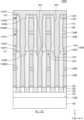
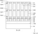
도 1은 예시적인 실시예들에 따른 집적회로 장치(10)의 일부 구성을 나타내는 레이아웃도이다.FIG. 1 is a layout diagram showing a portion of an integrated circuit device (10) according to exemplary embodiments.
도 1을 참조하면, 각각 단축 및 장축을 가지는 비교적 긴 아일랜드 형상을 갖는 복수의 활성 영역(AC)이 배치될 수 있다. 복수의 워드 라인(WL)은 복수의 활성 영역(AC)을 가로지르며 제1 방향(X 방향)을 따라 연장될 수 있다. 복수의 워드 라인(WL) 사이에 배치되는 활성 영역(AC)의 일부분 상에 다이렉트 콘택(DC)이 배치될 수 있고, 다이렉트 콘택(DC) 상에서 복수의 비트 라인(BL)이 제2 방향(Y 방향)을 따라 연장될 수 있다. 복수의 비트 라인(BL) 사이에 배치되는 활성 영역(AC)의 일부분 상에 배리드 콘택(BC)이 배치될 수 있고, 배리드 콘택(BC) 상에 하부 전극(LE)이 배치될 수 있다. 하부 전극(LE)과 배리드 콘택(BC) 상에는 선택적으로 랜딩 패드(LP)가 배치될 수 있다.Referring to FIG. 1, a plurality of active regions (AC) each having a relatively long island shape having a short axis and a long axis may be arranged. A plurality of word lines (WL) may extend along a first direction (X direction) while crossing the plurality of active regions (AC). A direct contact (DC) may be arranged on a portion of the active region (AC) arranged between the plurality of word lines (WL), and a plurality of bit lines (BL) may extend along a second direction (Y direction) on the direct contact (DC). A buried contact (BC) may be arranged on a portion of the active region (AC) arranged between the plurality of bit lines (BL), and a lower electrode (LE) may be arranged on the buried contact (BC). A landing pad (LP) may be selectively arranged on the lower electrode (LE) and the buried contact (BC).
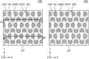
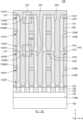
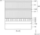
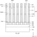
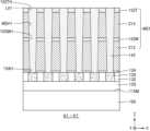
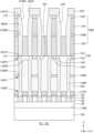
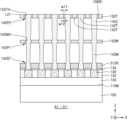
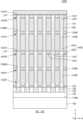
도 2는 예시적인 실시예들에 따른 집적회로 장치(100)의 일부 구성을 나타내는 평면도들이다. 도 2의 좌측도는 제1 수직 레벨(LV1)에서의 평면도이고, 도 2의 우측도는 제2 수직 레벨(LV2)에서의 평면도이다. 도 3a는 도 2의 도 A1-A1' 선에 따른 단면도이고, 도 3b는 도 2의 도 B1-B1' 선에 따른 단면도이며, 도 3c는 도 3b의 CX1 부분의 확대도이고, 도 3d는 도 3b의 CX2 부분의 확대도이다.FIG. 2 is a plan view showing a part of the configuration of an integrated circuit device (100) according to exemplary embodiments. The left side of FIG. 2 is a plan view at a first vertical level (LV1), and the right side of FIG. 2 is a plan view at a second vertical level (LV2). FIG. 3a is a cross-sectional view taken along line A1-A1' of FIG. 2, FIG. 3b is a cross-sectional view taken along line B1-B1' of FIG. 2, FIG. 3c is an enlarged view of a portion CX1 of FIG. 3b, and FIG. 3d is an enlarged view of a portion CX2 of FIG. 3b.
도 2 내지 도 3d을 참조하면, 집적회로 장치(100)는 도 1에 도시된 집적회로 장치(10)의 일부분에 해당할 수 있다. 기판(110)은 소자 분리막(도시 생략)에 의해 정의되는 활성 영역(AC)(도 1 참조)을 구비할 수 있다. 예시적인 실시예들에서, 기판(110)은 Si, Ge, 또는 SiGe, SiC, GaAs, InAs, 또는 InP와 같은 반도체 물질을 포함할 수 있다. 예시적인 실시예들에서, 기판(110)은 도전 영역, 예를 들면 불순물이 도핑된 웰 (well), 또는 불순물이 도핑된 구조물을 포함할 수 있다.Referring to FIGS. 2 to 3d, the integrated circuit device (100) may correspond to a portion of the integrated circuit device (10) illustrated in FIG. 1. The substrate (110) may have an active area (AC) (see FIG. 1) defined by a device isolation film (not illustrated). In exemplary embodiments, the substrate (110) may include a semiconductor material such as Si, Ge, or SiGe, SiC, GaAs, InAs, or InP. In exemplary embodiments, the substrate (110) may include a conductive area, for example, a well doped with an impurity, or a structure doped with an impurity.
도시되지는 않았으나, 기판(110)에는 제1 방향(X 방향)으로 연장되는 복수의 게이트 라인 트렌치(도시 생략)가 형성되고, 상기 복수의 게이트 라인 트렌치 내에 복수의 워드 라인(WL)(도 1 참조)이 배치될 수 있다. 복수의 워드 라인(WL)은 게이트 절연층(도시 생략) 및 게이트 전극(도시 생략)을 포함할 수 있다.Although not illustrated, a plurality of gate line trenches (not illustrated) extending in a first direction (X direction) may be formed in the substrate (110), and a plurality of word lines (WL) (see FIG. 1) may be arranged within the plurality of gate line trenches. The plurality of word lines (WL) may include a gate insulating layer (not illustrated) and a gate electrode (not illustrated).
기판(110)의 상면(110M) 상에는 하부 구조물(120)이 배치될 수 있다. 예를 들어, 하부 구조물(120) 내에 도 1을 참조로 설명한 복수의 비트 라인(BL), 배리드 콘택(BC), 및 다이렉트 콘택(DC)이 포함될 수 있다.A lower structure (120) may be arranged on the upper surface (110M) of the substrate (110). For example, a plurality of bit lines (BL), buried contacts (BC), and direct contacts (DC) described with reference to FIG. 1 may be included within the lower structure (120).
하부 구조물(120) 상에는 랜딩 패드(130)가 배치될 수 있다. 랜딩 패드(130)는 도 1을 참조로 설명한 랜딩 패드(LP)에 대응될 수 있고, 제1 방향(X 방향) 및 제2 방향(Y 방향)에 따라 소정의 간격으로 이격되어 배치될 수 있다. 랜딩 패드(130)의 측벽은 노드 분리 절연층(132)에 의해 둘러싸일 수 있고, 다이렉트 콘택(DC)을 통해 활성 영역(AC)에 전기적으로 연결될 수 있다. 랜딩 패드(130)는 루테늄(Ru), 티타늄(Ti), 탄탈륨(Ta), 니오븀(Nb), 이리듐(Ir), 몰리브덴(Mo), 텅스텐(W) 등의 금속, 티타늄 질화물(TiN), 탄탈륨 질화물(TaN), 니오븀 질화물(NbN), 몰리브덴 질화물(MoN), 텅스텐 질화물(WN) 등의 도전성 금속 질화물 중 적어도 하나를 포함할 수 있다. 일부 예시에서, 랜딩 패드(130)는 티타늄 질화물(TiN)을 포함할 수 있다.A landing pad (130) may be arranged on the lower structure (120). The landing pad (130) may correspond to the landing pad (LP) described with reference to FIG. 1, and may be arranged spaced apart at a predetermined interval along the first direction (X direction) and the second direction (Y direction). The side wall of the landing pad (130) may be surrounded by a node separation insulating layer (132) and may be electrically connected to the active area (AC) through a direct contact (DC). The landing pad (130) may include at least one of a metal such as ruthenium (Ru), titanium (Ti), tantalum (Ta), niobium (Nb), iridium (Ir), molybdenum (Mo), tungsten (W), or a conductive metal nitride such as titanium nitride (TiN), tantalum nitride (TaN), niobium nitride (NbN), molybdenum nitride (MoN), or tungsten nitride (WN). In some examples, the landing pad (130) may include titanium nitride (TiN).
랜딩 패드(130) 및 노드 분리 절연층(132) 상에는 식각 정지층(134)이 형성될 수 있다. 식각 정지층(134)은 랜딩 패드(130)의 상면을 노출하는 개구부(134H)를 구비할 수 있다.An etching stop layer (134) may be formed on the landing pad (130) and the node separation insulating layer (132). The etching stop layer (134) may have an opening (134H) that exposes the upper surface of the landing pad (130).
식각 정지층(134) 상에는 커패시터 구조물(CS)이 배치될 수 있다. 커패시터 구조물(CS)은 랜딩 패드(130)에 전기적으로 연결되는 하부 전극(140), 하부 전극(140)을 콘포말하게 커버하는 유전층(160), 및 유전층(160) 상의 상부 전극(170)을 포함할 수 있다.A capacitor structure (CS) may be arranged on the etching stop layer (134). The capacitor structure (CS) may include a lower electrode (140) electrically connected to the landing pad (130), a dielectric layer (160) conformally covering the lower electrode (140), and an upper electrode (170) on the dielectric layer (160).
하부 전극(140)은 랜딩 패드(130) 상에 배치될 수 있고, 하부 전극(140)의 바닥부는 식각 정지층(134)의 개구부(134H) 내에 배치될 수 있다. 하부 전극(140)의 바닥부 폭은 랜딩 패드(130)의 폭보다 더 작을 수 있고, 이에 따라 하부 전극(140)의 바닥면 전체가 랜딩 패드(130)와 접촉할 수 있다.The lower electrode (140) may be placed on the landing pad (130), and the bottom of the lower electrode (140) may be placed within the opening (134H) of the etching stop layer (134). The width of the bottom of the lower electrode (140) may be smaller than the width of the landing pad (130), and thus, the entire bottom surface of the lower electrode (140) may be in contact with the landing pad (130).
예시적인 실시예들에서, 하부 전극(140)은 랜딩 패드(130) 상에 배치되는 제1 하부 전극부(142)와, 제1 하부 전극부(142) 상에 배치되는 제2 하부 전극부(144)를 포함할 수 있다. 제1 하부 전극부(142)와 제2 하부 전극부(144)는 기판(110)의 상면(110M)에 수직한 제3 방향(Z 방향)을 따라 상대적으로 큰 높이로 연장될 수 있다.In exemplary embodiments, the lower electrode (140) may include a first lower electrode portion (142) disposed on the landing pad (130) and a second lower electrode portion (144) disposed on the first lower electrode portion (142). The first lower electrode portion (142) and the second lower electrode portion (144) may extend to a relatively large height along a third direction (Z direction) perpendicular to the upper surface (110M) of the substrate (110).
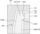
제1 하부 전극부(142)는 제1 메인 영역(142M)과 제1 탑 영역(142T)을 포함할 수 있다. 제1 하부 전극부(142)의 제1 탑 영역(142T)은 제1 탑 지지 패턴(152T)에 의해 둘러싸일 수 있고, 제1 하부 전극부(142)의 제1 메인 영역(142M)의 측벽 일부분은 제1 중간 지지 패턴(152M)에 의해 둘러싸일 수 있다. 예를 들어 제1 탑 지지 패턴(152T)은 제1 개구부(152TH)를 포함하고, 제1 개구부(152TH) 내에 제1 하부 전극부(142)의 제1 탑 영역(142T)이 배치될 수 있다. 예를 들어 제1 중간 지지 패턴(152M)은 제2 개구부(152MH)를 포함하고, 제1 하부 전극부(142)의 제1 메인 영역(142M)의 측벽 일부분이 제2 개구부(152MH) 내에 배치될 수 있다. 제1 탑 지지 패턴(152T) 및 제1 중간 지지 패턴(152M)은 상대적으로 높은 종횡비를 갖는 제1 하부 전극부(142)가 인접한 제1 하부 전극부(142)를 향해 기울어지거나 쓰러지는 것을 방지하는 지지 부재 역할을 할 수 있다.The first lower electrode portion (142) may include a first main region (142M) and a first top region (142T). The first top region (142T) of the first lower electrode portion (142) may be surrounded by a first top support pattern (152T), and a portion of a side wall of the first main region (142M) of the first lower electrode portion (142) may be surrounded by a first middle support pattern (152M). For example, the first top support pattern (152T) may include a first opening (152TH), and the first top region (142T) of the first lower electrode portion (142) may be arranged within the first opening (152TH). For example, the first middle support pattern (152M) may include a second opening (152MH), and a portion of a sidewall of the first main region (142M) of the first lower electrode portion (142) may be positioned within the second opening (152MH). The first top support pattern (152T) and the first middle support pattern (152M) may serve as support members to prevent the first lower electrode portion (142) having a relatively high aspect ratio from tilting or collapsing toward the adjacent first lower electrode portion (142).
예시적인 실시예들에서, 도 3a에서 도시되는 것과 같이 제1 탑 지지 패턴(152T)의 상면은 제1 수직 레벨(LV1)에 배치될 수 있고, 제1 탑 영역(142T)의 상면은 제1 탑 지지 패턴(152T)의 상면과 동일한 레벨에(즉, 제1 수직 레벨(LV1)에) 배치될 수 있다. 이와는 달리, 도 3a에서 도시되는 것과 달리 제1 탑 영역(142T)의 상면은 제1 탑 지지 패턴(152T)의 상면보다 높은 레벨에(즉, 제1 수직 레벨(LV1)보다 높은 레벨에) 배치될 수도 있다.In exemplary embodiments, as illustrated in FIG. 3A, the upper surface of the first top support pattern (152T) may be disposed at the first vertical level (LV1), and the upper surface of the first top region (142T) may be disposed at the same level as the upper surface of the first top support pattern (152T) (i.e., at the first vertical level (LV1)). Alternatively, unlike as illustrated in FIG. 3A, the upper surface of the first top region (142T) may be disposed at a level higher than the upper surface of the first top support pattern (152T) (i.e., at a level higher than the first vertical level (LV1)).
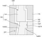
제2 하부 전극부(144)는 제2 메인 영역(144M)과 제2 탑 영역(144T)을 포함할 수 있다. 제2 메인 영역(144M)은 제1 하부 전극부(142)의 제1 탑 영역(142T)의 상면 상에 배치될 수 있고, 제1 하부 전극부(142)의 연장 방향과 동일한 방향으로 연장될 수 있다. 제2 하부 전극부(144)의 제2 탑 영역(144T)은 제2 탑 지지 패턴(154T)에 의해 둘러싸일 수 있고, 제2 하부 전극부(144)의 제2 메인 영역(144M)의 측벽 일부분은 제2 중간 지지 패턴(154M)에 의해 둘러싸일 수 있다. 예를 들어 제2 탑 지지 패턴(154T)은 제3 개구부(154TH)를 포함하고, 제3 개구부(154TH) 내에 제2 하부 전극부(144)의 제2 탑 영역(144T)이 배치될 수 있다. 예를 들어 제2 중간 지지 패턴(154M)은 제4 개구부(154MH)를 포함하고, 제2 하부 전극부(144)의 제2 메인 영역(144M)의 측벽 일부분이 제4 개구부(154MH) 내에 배치될 수 있다.The second lower electrode portion (144) may include a second main region (144M) and a second top region (144T). The second main region (144M) may be disposed on an upper surface of the first top region (142T) of the first lower electrode portion (142) and may extend in the same direction as the extension direction of the first lower electrode portion (142). The second top region (144T) of the second lower electrode portion (144) may be surrounded by a second top support pattern (154T), and a portion of a side wall of the second main region (144M) of the second lower electrode portion (144) may be surrounded by a second intermediate support pattern (154M). For example, the second top support pattern (154T) may include a third opening (154TH), and the second top region (144T) of the second lower electrode portion (144) may be positioned within the third opening (154TH). For example, the second middle support pattern (154M) may include a fourth opening (154MH), and a portion of a side wall of the second main region (144M) of the second lower electrode portion (144) may be positioned within the fourth opening (154MH).
예시적인 실시예들에서, 도 3a에서 도시되는 것과 같이 제2 탑 지지 패턴(154T)의 상면은 제2 수직 레벨(LV2)에 배치될 수 있고, 제2 탑 영역(144T)의 상면은 제2 탑 지지 패턴(154T)의 상면과 동일한 레벨에(즉, 제2 수직 레벨(LV2)에) 배치될 수 있다. 이와는 달리, 도 3a에서 도시되는 것과 달리 제2 탑 영역(144T)의 상면은 제2 탑 지지 패턴(154T)의 상면보다 높은 레벨에(즉, 제2 수직 레벨(LV2)보다 높은 레벨에) 배치될 수도 있다.In exemplary embodiments, as illustrated in FIG. 3A, the upper surface of the second top support pattern (154T) may be disposed at the second vertical level (LV2), and the upper surface of the second top region (144T) may be disposed at the same level as the upper surface of the second top support pattern (154T) (i.e., at the second vertical level (LV2)). Alternatively, unlike as illustrated in FIG. 3A, the upper surface of the second top region (144T) may be disposed at a level higher than the upper surface of the second top support pattern (154T) (i.e., at a level higher than the second vertical level (LV2)).
제1 하부 전극부(142)의 제1 메인 영역(142M)은 제1 중간 지지 패턴(152M)에 접하는 제1 돌출부(142P1)를 포함할 수 있고, 제1 하부 전극부(142)의 제1 탑 영역(142T)은 제1 탑 지지 패턴(152T)에 접하는 제2 돌출부(142P2)를 포함할 수 있다. 제1 돌출부(142P1) 및 제2 돌출부(142P2)는 제1 메인 영역(142M)의 측벽에 대하여 외측으로 돌출할 수 있고, 제1 돌출부(142P1)는 제1 중간 지지 패턴(152M)에 의해 둘러싸이고, 제2 돌출부(142P2)는 제1 탑 지지 패턴(152T)에 의해 둘러싸일 수 있다. 제1 탑 영역(142T)이 제2 돌출부(142P2)를 포함하므로, 제1 탑 영역(142T)의 제1 방향(X 방향)에 따른 폭이 제1 메인 영역(142M)의 제1 방향(X 방향)에 따른 폭보다 더 클 수 있다.The first main region (142M) of the first lower electrode portion (142) may include a first protrusion (142P1) that contacts the first middle support pattern (152M), and the first top region (142T) of the first lower electrode portion (142) may include a second protrusion (142P2) that contacts the first top support pattern (152T). The first protrusion (142P1) and the second protrusion (142P2) may protrude outwardly with respect to a side wall of the first main region (142M), and the first protrusion (142P1) may be surrounded by the first middle support pattern (152M), and the second protrusion (142P2) may be surrounded by the first top support pattern (152T). Since the first top region (142T) includes the second protrusion (142P2), the width of the first top region (142T) in the first direction (X direction) may be larger than the width of the first main region (142M) in the first direction (X direction).
제1 하부 전극부(142)의 제1 메인 영역(142M)은 그 측벽에 단차부(142ST)를 포함할 수 있다. 단차부(142ST)는 제1 중간 지지 패턴(152M)의 바닥면보다 낮은 레벨에 형성될 수 있다.The first main region (142M) of the first lower electrode portion (142) may include a step portion (142ST) on its side wall. The step portion (142ST) may be formed at a level lower than the bottom surface of the first intermediate support pattern (152M).
예시적인 제조 공정에 따르면, 단차부(142ST)는 제1 하부 전극부(142)의 측벽으로부터 소정의 두께만큼을 제거하는 제1 트리밍 공정에 의해 형성되며, 이 때 제1 중간 지지 패턴(152M)에 의해 둘러싸이는 제1 하부 전극부(142)의 측벽 일부분이 제거되지 않아 제1 돌출부(142P1)가 형성될 수 있고, 제1 탑 지지 패턴(152T)에 의해 둘러싸이는 제1 하부 전극부(142)의 제1 탑 영역(142T)의 측벽 부분이 제거되지 않아 제2 돌출부(142P2)가 형성될 수 있다.According to an exemplary manufacturing process, the step portion (142ST) is formed by a first trimming process of removing a predetermined thickness from a sidewall of the first lower electrode portion (142), and at this time, a part of the sidewall of the first lower electrode portion (142) surrounded by the first middle support pattern (152M) is not removed, so that a first protrusion portion (142P1) can be formed, and a part of the sidewall of the first top region (142T) of the first lower electrode portion (142) surrounded by the first top support pattern (152T) is not removed, so that a second protrusion portion (142P2) can be formed.
제2 하부 전극부(144)의 제2 메인 영역(144M)은 제2 중간 지지 패턴(154M)에 접하는 제3 돌출부(144P1)를 포함할 수 있고, 제2 하부 전극부(144)의 제2 탑 영역(144T)은 제2 탑 지지 패턴(154T)에 접하는 제4 돌출부(144P2)를 포함할 수 있다. 제3 돌출부(144P1) 및 제4 돌출부(144P2)는 제2 메인 영역(144M)의 측벽에 대하여 외측으로 돌출할 수 있고, 제3 돌출부(144P1)는 제2 중간 지지 패턴(154M)에 의해 둘러싸이고, 제4 돌출부(144P2)는 제2 탑 지지 패턴(154T)에 의해 둘러싸일 수 있다. 제2 탑 영역(144T)이 제4 돌출부(144P2)를 포함하므로, 제2 탑 영역(144T)의 제1 방향(X 방향)에 따른 폭이 제2 메인 영역(144M)의 제1 방향(X 방향)에 따른 폭보다 더 클 수 있다.The second main region (144M) of the second lower electrode portion (144) may include a third protrusion (144P1) that contacts the second middle support pattern (154M), and the second top region (144T) of the second lower electrode portion (144) may include a fourth protrusion (144P2) that contacts the second top support pattern (154T). The third protrusion (144P1) and the fourth protrusion (144P2) may protrude outwardly with respect to a side wall of the second main region (144M), and the third protrusion (144P1) may be surrounded by the second middle support pattern (154M), and the fourth protrusion (144P2) may be surrounded by the second top support pattern (154T). Since the second top region (144T) includes the fourth protrusion (144P2), the width of the second top region (144T) in the first direction (X direction) may be larger than the width of the second main region (144M) in the first direction (X direction).
또한 제2 하부 전극부(144)의 제2 메인 영역(144M)은 그 측벽에 단차부(144ST)를 포함할 수 있다. 단차부(144ST)는 제2 중간 지지 패턴(154M)의 바닥면보다 낮은 레벨에 형성될 수 있다.Additionally, the second main region (144M) of the second lower electrode portion (144) may include a step portion (144ST) on its side wall. The step portion (144ST) may be formed at a level lower than the bottom surface of the second intermediate support pattern (154M).
예시적인 제조 공정에 따르면, 단차부(144ST)는 제2 하부 전극부(144)의 측벽으로부터 소정의 두께만큼을 제거하는 제2 트리밍 공정에 의해 형성될 수 있다. 제2 트리밍 공정은 제1 트리밍 공정과는 별개로 수행될 수 있고, 즉 제2 트리밍 공정은 제1 트리밍 공정과 동시에 수행되지 않을 수 있다. 이 때 제2 중간 지지 패턴(154M)에 의해 둘러싸이는 제2 하부 전극부(144)의 측벽 일부분이 제거되지 않아 제3 돌출부(144P1)가 형성될 수 있고, 제2 탑 지지 패턴(154T)에 의해 둘러싸이는 제2 하부 전극부(144)의 제2 탑 영역(144T)의 측벽 부분이 제거되지 않아 제4 돌출부(144P2)가 형성될 수 있다.According to an exemplary manufacturing process, the step portion (144ST) may be formed by a second trimming process that removes a predetermined thickness from a sidewall of the second lower electrode portion (144). The second trimming process may be performed separately from the first trimming process, that is, the second trimming process may not be performed simultaneously with the first trimming process. In this case, a part of the sidewall of the second lower electrode portion (144) surrounded by the second middle support pattern (154M) may not be removed, thereby forming a third protrusion (144P1), and a part of the sidewall of the second top region (144T) of the second lower electrode portion (144) surrounded by the second top support pattern (154T) may not be removed, thereby forming a fourth protrusion (144P2).
도 2 및 도 3b에 도시되는 것과 같이, 제1 탑 지지 패턴(152T)은 제1 몰드 개구부(OP1)를 정의할 수 있다. 제1 하부 전극부(142)는 제1 탑 영역(142T)에 형성된 경사면(142XS)을 포함하고, 경사면(142XS)은 제1 몰드 개구부(OP1)에 노출되고 제1 탑 지지 패턴(152T)에 의해 둘러싸이지 않을 수 있다. 제1 하부 전극부(142)의 경사면(142XS)에 대하여 제2 하부 전극부(144)의 바닥부는 외측으로 돌출할 수 있다.As illustrated in FIGS. 2 and 3B, the first top support pattern (152T) may define a first mold opening (OP1). The first lower electrode portion (142) may include an inclined surface (142XS) formed in the first top region (142T), and the inclined surface (142XS) may be exposed to the first mold opening (OP1) and may not be surrounded by the first top support pattern (152T). The bottom of the second lower electrode portion (144) may protrude outward with respect to the inclined surface (142XS) of the first lower electrode portion (142).
예시적인 제조 공정에 따르면, 제1 탑 지지 패턴(152T)을 식각하여 제1 몰드 개구부(OP1)를 형성하고, 이후 제1 몰드 개구부(OP1)에 의해 노출된 제1 하부 전극부(142)의 제1 탑 영역(142T)의 노출 부분을 트리밍하는 공정에 의해 경사면(142XS)이 형성될 수 있다. 이러한 트리밍 공정에 의해, 제1 하부 전극부(142)의 제1 탑 영역(142T)과 이에 인접한 제1 하부 전극부(142)의 제1 탑 영역(142T) 사이의 거리가 증가될 수 있고, 제1 몰드 개구부(OP1)를 통한 에천트 등의 물질의 공급이 용이해질 수 있다.According to an exemplary manufacturing process, a first top support pattern (152T) is etched to form a first mold opening (OP1), and then an inclined surface (142XS) may be formed by a process of trimming an exposed portion of a first top region (142T) of a first lower electrode portion (142) exposed by the first mold opening (OP1). By this trimming process, a distance between the first top region (142T) of the first lower electrode portion (142) and the first top region (142T) of the first lower electrode portion (142) adjacent thereto may be increased, and supply of a material such as an etchant through the first mold opening (OP1) may be facilitated.
도 2 및 도 3b에 도시되는 것과 같이, 제2 탑 지지 패턴(154T)은 제2 몰드 개구부(OP2)를 정의할 수 있다. 제2 하부 전극부(144)는 제2 탑 영역(144T)에 형성된 경사면(144XS)을 포함하고, 경사면(144XS)은 제2 몰드 개구부(OP2)에 노출되고 제2 탑 지지 패턴(154T)에 의해 둘러싸이지 않을 수 있다.As illustrated in FIGS. 2 and 3b, the second top support pattern (154T) may define a second mold opening (OP2). The second lower electrode portion (144) may include an inclined surface (144XS) formed in the second top region (144T), and the inclined surface (144XS) may be exposed to the second mold opening (OP2) and may not be surrounded by the second top support pattern (154T).
예시적인 제조 공정에 따르면, 제2 탑 지지 패턴(154T)을 식각하여 제2 몰드 개구부(OP2)를 형성하고, 이후 제2 몰드 개구부(OP2)에 의해 노출된 제2 하부 전극부(144)의 제2 탑 영역(144T)의 노출 부분을 트리밍하는 공정에 의해 경사면(144XS)이 형성될 수 있다. 경사면(144XS)을 형성하기 위한 트리밍 공정은, 경사면(142XS)을 형성하기 위한 트리밍 공정과는 별개로 수행될 수 있다(예를 들어, 경사면(144XS)을 형성하기 위한 트리밍 공정은 경사면(142XS)을 형성하기 위한 트리밍 공정과 동시에 수행되지 않을 수 있다).According to an exemplary manufacturing process, a second top support pattern (154T) is etched to form a second mold opening (OP2), and then an inclined surface (144XS) may be formed by a process of trimming an exposed portion of a second top region (144T) of a second lower electrode portion (144) exposed by the second mold opening (OP2). The trimming process for forming the inclined surface (144XS) may be performed separately from the trimming process for forming the inclined surface (142XS) (for example, the trimming process for forming the inclined surface (144XS) may not be performed simultaneously with the trimming process for forming the inclined surface (142XS)).
도 2 및 도 3a에 도시된 것과 같이, 제1 하부 전극부(142)와 제2 하부 전극부(144)는 수직 방향(Z 방향)으로 연장하는 필라 또는 기둥 형상일 수 있다. 제1 탑 지지 패턴(152T)의 바닥면보다 낮은 수직 레벨에서 제1 하부 전극부(142)의 수평 단면은 원형을 가질 수 있고, 제1 수직 레벨(LV1)에서 제1 하부 전극부(142)의 수평 단면은 경사면(142XS)에 의해 정의되는, 원형이 아닌 일부분을 포함할 수 있다. 제2 탑 지지 패턴(154T)의 바닥면보다 낮은 수직 레벨에서 제2 하부 전극부(144)의 수평 단면은 원형을 가질 수 있고, 제2 수직 레벨(LV2)에서 제2 하부 전극부(144)의 수평 단면은 경사면(144XS)에 의해 정의되는, 원형이 아닌 일부분을 포함할 수 있다.As illustrated in FIGS. 2 and 3A, the first lower electrode portion (142) and the second lower electrode portion (144) may have a pillar or column shape extending in the vertical direction (Z direction). A horizontal cross-section of the first lower electrode portion (142) at a vertical level lower than the bottom surface of the first top support pattern (152T) may have a circular shape, and the horizontal cross-section of the first lower electrode portion (142) at the first vertical level (LV1) may include a non-circular portion defined by the inclined plane (142XS). A horizontal cross-section of the second lower electrode portion (144) at a vertical level lower than the bottom surface of the second top support pattern (154T) may have a circular shape, and the horizontal cross-section of the second lower electrode portion (144) at the second vertical level (LV2) may include a non-circular portion defined by the inclined plane (144XS).
예시적인 실시예들에서, 제1 하부 전극부(142)와 제2 하부 전극부(144)는 루테늄(Ru), 티타늄(Ti), 탄탈륨(Ta), 니오븀(Nb), 이리듐(Ir), 몰리브덴(Mo), 텅스텐(W) 등의 금속, 티타늄 질화물(TiN), 탄탈륨 질화물(TaN), 니오븀 질화물(NbN), 몰리브덴 질화물(MoN), 텅스텐 질화물(WN) 등의 도전성 금속 질화물, 및 이리듐 산화물(IrO2), 루테늄 산화물(RuO2), 스트론튬 루테늄 산화물(SrRuO3), 등의 도전성 금속 산화물 중에서 선택된 적어도 하나를 포함할 수 있다.In exemplary embodiments, the first lower electrode portion (142) and the second lower electrode portion (144) may include at least one selected from a metal such as ruthenium (Ru), titanium (Ti), tantalum (Ta), niobium (Nb), iridium (Ir), molybdenum (Mo), tungsten (W), a conductive metal nitride such as titanium nitride (TiN), tantalum nitride (TaN), niobium nitride (NbN), molybdenum nitride (MoN), tungsten nitride (WN), and a conductive metal oxide such as iridium oxide (IrO2 ), ruthenium oxide (RuO2 ), strontium ruthenium oxide (SrRuO3 ).
제1 탑 지지 패턴(152T), 제1 중간 지지 패턴(152M), 제2 탑 지지 패턴(154T), 및 제2 중간 지지 패턴(154M)은 실리콘 질화물, 실리콘 산질화물, 실리콘 보론 질화물(SiBN), 또는 실리콘 카본 질화물(SiCN)을 포함할 수 있다.The first top support pattern (152T), the first intermediate support pattern (152M), the second top support pattern (154T), and the second intermediate support pattern (154M) may include silicon nitride, silicon oxynitride, silicon boron nitride (SiBN), or silicon carbon nitride (SiCN).
하부 전극(140)의 측벽 및 상면 상에는 유전층(160)이 배치될 수 있다. 유전층(160)은 하부 전극(140)의 측벽으로부터 제1 탑 지지 패턴(152T), 제1 중간 지지 패턴(152M), 제2 탑 지지 패턴(154T), 및 제2 중간 지지 패턴(154M)의 상면들 및 바닥면들 상으로 연장될 수 있고, 식각 정지층(134) 상에도 배치될 수 있다. 유전층(160)은 하부 전극(140)의 상면에 수직한 방향을 따라 약 20 내지 100 Å의 두께를 가질 수 있으나, 이에 한정되는 것은 아니다.A dielectric layer (160) may be disposed on the sidewall and upper surface of the lower electrode (140). The dielectric layer (160) may extend from the sidewall of the lower electrode (140) onto the upper surfaces and bottom surfaces of the first top support pattern (152T), the first middle support pattern (152M), the second top support pattern (154T), and the second middle support pattern (154M), and may also be disposed on the etch stop layer (134). The dielectric layer (160) may have a thickness of about 20 to 100 Å in a direction perpendicular to the upper surface of the lower electrode (140), but is not limited thereto.
예시적인 실시예들에서, 유전층(160)은 지르코늄 산화물, 하프늄 산화물, 티타늄 산화물, 니오븀 산화물, 탄탈륨 산화물, 이트륨 산화물, 스트론튬 티타늄 산화물, 바륨 스트론튬 티타늄 산화물, 스칸듐 산화물, 및 란탄족 산화물 중 적어도 하나를 포함할 수 있다.In exemplary embodiments, the dielectric layer (160) may include at least one of zirconium oxide, hafnium oxide, titanium oxide, niobium oxide, tantalum oxide, yttrium oxide, strontium titanium oxide, barium strontium titanium oxide, scandium oxide, and a lanthanide oxide.
유전층(160) 상에는 하부 전극(140)을 커버하는 상부 전극(170)이 배치될 수 있다. 상부 전극(170)은 루테늄(Ru), 티타늄(Ti), 탄탈륨(Ta), 니오븀(Nb), 이리듐(Ir), 몰리브덴(Mo), 텅스텐(W) 등의 금속, 티타늄 질화물(TiN), 탄탈륨 질화물(TaN), 니오븀 질화물(NbN), 몰리브덴 질화물(MoN), 텅스텐 질화물(WN) 등의 도전성 금속 질화물, 및 이리듐 산화물(IrO2), 루테늄 산화물(RuO2), 스트론튬 루테늄 산화물(SrRuO3), 등의 도전성 금속 산화물 중에서 선택된 적어도 하나를 포함할 수 있다.An upper electrode (170) covering the lower electrode (140) may be arranged on the dielectric layer (160). The upper electrode (170) may include at least one selected from metals such as ruthenium (Ru), titanium (Ti), tantalum (Ta), niobium (Nb), iridium (Ir), molybdenum (Mo), and tungsten (W); conductive metal nitrides such as titanium nitride (TiN), tantalum nitride (TaN), niobium nitride (NbN), molybdenum nitride (MoN), and tungsten nitride (WN); and conductive metal oxides such as iridium oxide (IrO2 ), ruthenium oxide (RuO2 ), and strontium ruthenium oxide (SrRuO3 ).
선택적으로, 유전층(160)과 상부 전극(170) 사이에는 계면층(도시 생략)이 더 형성될 수 있다. 상기 계면층은 티타늄 산화물, 탄탈륨 산화물, 니오븀 산화물, 몰리브덴 산화물, 이리듐 산화물, 등의 금속 산화물, 또는 티타늄 산화질화물(TiON), 탄탈륨 산화질화물(TaON), 니오븀 산화질화물(NbON), 몰리브덴 산화질화물(MoON) 등의 금속 산질화물 중 적어도 하나를 포함할 수 있다.Optionally, an interface layer (not shown) may be further formed between the dielectric layer (160) and the upper electrode (170). The interface layer may include at least one of a metal oxide such as titanium oxide, tantalum oxide, niobium oxide, molybdenum oxide, iridium oxide, or a metal oxynitride such as titanium oxynitride (TiON), tantalum oxynitride (TaON), niobium oxynitride (NbON), or molybdenum oxynitride (MoON).
일반적으로, 하부 전극의 종횡비가 커짐에 따라 몰드 스택의 개구부를 형성하는 공정에서 사용되는 마스크 패턴의 높이도 커질 필요가 있으며, 이에 따라 개구부의 프로파일을 정밀하게 조절하기 어려운 문제가 있다. 특히 개구부의 상측 폭이 바닥부 폭보다 더 크게 형성되는 경우에 개구부 내를 채우는 하부 전극이 인접한 하부 전극과 연결되어 브릿지 불량이 발생하거나, 하부 전극의 국부적으로 큰 볼륨에 기인하여, 이에 인접한 유전층을 통한 누설 전류가 발생하는 문제가 있다.In general, as the aspect ratio of the lower electrode increases, the height of the mask pattern used in the process of forming the opening of the mold stack also needs to increase, which makes it difficult to precisely control the profile of the opening. In particular, when the upper width of the opening is formed larger than the bottom width, the lower electrode filling the inside of the opening may be connected to the adjacent lower electrode, resulting in a bridge defect, or a leakage current may occur through the adjacent dielectric layer due to the locally large volume of the lower electrode.
그러나 전술한 예시적인 실시예들에 따르면, 하부 전극(140)은 제1 하부 전극부(142)와 제2 하부 전극부(144)를 포함하는 구조로 형성됨에 따라, 하부 전극(140)의 높이를 증가시킬 수 있어 집적회로 장치(100)는 향상된 커패시턴스를 가질 수 있다. 또한 제1 하부 전극부(142)의 측벽의 폭을 감소시키기 위한 트리밍 공정과 제2 하부 전극부(144)의 측벽의 폭을 감소시키기 위한 트리밍 공정이 수행됨에 따라, 제1 하부 전극부(142)와 제2 하부 전극부(144)는 이에 인접한 제1 하부 전극부(142)와 제2 하부 전극부(144)와의 충분한 이격거리가 확보될 수 있다. 따라서 하부 전극(140)의 브릿지 불량의 발생 또는 누설 전류의 발생이 방지될 수 있고, 상기 집적회로 장치(100)는 우수한 전기적 특성을 가질 수 있다.However, according to the exemplary embodiments described above, since the lower electrode (140) is formed with a structure including the first lower electrode portion (142) and the second lower electrode portion (144), the height of the lower electrode (140) can be increased, so that the integrated circuit device (100) can have improved capacitance. In addition, since the trimming process for reducing the width of the sidewall of the first lower electrode portion (142) and the trimming process for reducing the width of the sidewall of the second lower electrode portion (144) are performed, a sufficient separation distance between the first lower electrode portion (142) and the second lower electrode portion (144) and the adjacent first lower electrode portion (142) and second lower electrode portion (144) can be secured. Therefore, the occurrence of bridge failure of the lower electrode (140) or the occurrence of leakage current can be prevented, and the integrated circuit device (100) can have excellent electrical characteristics.
도 4는 예시적인 실시예들에 따른 집적회로 장치(100A)를 나타내는 단면도이다. 도 4는 도 2의 A1-A1' 단면에 대응되는 단면을 나타낸다. 도 4에서 도 1 내지 도 3d에서와 동일한 참조부호는 동일한 구성요소를 의미한다.Fig. 4 is a cross-sectional view showing an integrated circuit device (100A) according to exemplary embodiments. Fig. 4 shows a cross-section corresponding to the A1-A1' cross-section of Fig. 2. In Fig. 4, the same reference numerals as in Figs. 1 to 3d denote the same components.
도 4를 참조하면, 하부 전극(140A)은 제1 하부 전극부(142A)와 제2 하부 전극부(144A)를 포함한다. 제1 하부 전극부(142A)는 제1 중간 지지 패턴(152M)에 의해 둘러싸이는 제1 돌출부(142P1A)를 포함하나, 제1 중간 지지 패턴(152M)보다 낮은 레벨에 배치되는 단차부(142ST)(도 3a 참조)는 형성되지 않는다. 또한 제1 돌출부(142P1A)는 제1 중간 지지 패턴(152M)보다 더 높은 레벨에 배치되는 제1 하부 전극부(142A)의 제1 메인 영역(142M)의 측벽에 대하여 외측으로 돌출하고, 제1 중간 지지 패턴(152M)보다 더 낮은 레벨에 배치되는 제1 메인 영역(142M)의 측벽과 연속적으로 연결될 수 있다.Referring to FIG. 4, the lower electrode (140A) includes a first lower electrode portion (142A) and a second lower electrode portion (144A). The first lower electrode portion (142A) includes a first protrusion (142P1A) surrounded by a first intermediate support pattern (152M), but a step portion (142ST) (see FIG. 3A) disposed at a lower level than the first intermediate support pattern (152M) is not formed. In addition, the first protrusion (142P1A) may protrude outwardly with respect to a sidewall of a first main region (142M) of the first lower electrode portion (142A) disposed at a higher level than the first intermediate support pattern (152M), and may be continuously connected to a sidewall of the first main region (142M) disposed at a lower level than the first intermediate support pattern (152M).
예시적인 제조 공정에서, 제1 돌출부(142P1A)는 제1 하부 전극부(142A)의 측벽으로부터 소정의 두께만큼을 제거하는 제1 트리밍 공정에 의해 형성될 수 있다. 특히 제1 중간 지지 패턴(152M)보다 낮은 레벨에 배치되는 제1 하부 전극부(142A)의 측벽이 노출되지 않는 상태로 제1 중간 지지 패턴(152M) 상면보다 높은 레벨에 배치되는 제1 하부 전극부(142A)의 측벽에 제1 트리밍 공정을 수행하여 제1 돌출부(142P1A)와 제2 돌출부(142P2)가 형성될 수 있다. 제1 하부 전극부(142A)의 상측의 폭이 하측의 폭보다 상대적으로 클 때, 제1 트리밍 공정을 수행하여 제1 하부 전극부(142A)의 상측의 폭을 축소시킴으로써, 제1 하부 전극부(142A)의 브릿지 불량 발생 또는 누설 전류 발생이 방지될 수 있다.In an exemplary manufacturing process, the first protrusion (142P1A) may be formed by a first trimming process that removes a predetermined thickness from a sidewall of the first lower electrode portion (142A). In particular, the first trimming process may be performed on the sidewall of the first lower electrode portion (142A) that is disposed at a level higher than the upper surface of the first intermediate support pattern (152M) without exposing the sidewall of the first lower electrode portion (142A) that is disposed at a level lower than the first intermediate support pattern (152M), so that the first protrusion (142P1A) and the second protrusion (142P2) may be formed. When the width of the upper side of the first lower electrode portion (142A) is relatively larger than the width of the lower side, the first trimming process may be performed to reduce the width of the upper side of the first lower electrode portion (142A), thereby preventing the occurrence of a bridge defect or leakage current in the first lower electrode portion (142A).
또한 제1 하부 전극부(142A)와 유사하게, 제2 하부 전극부(144A)도 제2 중간 지지 패턴(154M)에 의해 둘러싸이는 제3 돌출부(144P1A)를 포함하나, 제2 중간 지지 패턴(154M)보다 낮은 레벨에 배치되는 단차부(144ST)(도 3a 참조)는 형성되지 않는다. 또한 제3 돌출부(144P1A)는 제2 중간 지지 패턴(154M)보다 더 높은 레벨에 배치되는 제2 하부 전극부(144A)의 제2 메인 영역(144M)의 측벽에 대하여 외측으로 돌출하고, 제2 중간 지지 패턴(154M)보다 더 낮은 레벨에 배치되는 제2 메인 영역(144M)의 측벽과 연속적으로 연결될 수 있다.Also, similarly to the first lower electrode portion (142A), the second lower electrode portion (144A) also includes a third protrusion (144P1A) surrounded by a second intermediate support pattern (154M), but a step portion (144ST) (see FIG. 3A) disposed at a lower level than the second intermediate support pattern (154M) is not formed. In addition, the third protrusion (144P1A) may protrude outwardly with respect to a sidewall of the second main region (144M) of the second lower electrode portion (144A) disposed at a higher level than the second intermediate support pattern (154M), and may be continuously connected to a sidewall of the second main region (144M) disposed at a lower level than the second intermediate support pattern (154M).
예시적인 제조 공정에서, 제3 돌출부(144P1A)는 제2 하부 전극부(144A)의 측벽으로부터 소정의 두께만큼을 제거하는 제2 트리밍 공정에 의해 형성될 수 있다. 특히 제2 중간 지지 패턴(154M)보다 낮은 레벨에 배치되는 제2 하부 전극부(144A)의 측벽이 노출되지 않는 상태로 제2 중간 지지 패턴(154M) 상면보다 높은 레벨에 배치되는 제2 하부 전극부(144A)의 측벽에 제2 트리밍 공정을 수행하여 제3 돌출부(144P1A)와 제4 돌출부(144P2)가 형성될 수 있다. 제2 트리밍 공정은 제1 트리밍 공정과는 별개로 수행될 수 있다(예를 들어 제1 트리밍 공정과 동시에 수행되지 않을 수 있다).In an exemplary manufacturing process, the third protrusion (144P1A) may be formed by a second trimming process that removes a predetermined thickness from a sidewall of the second lower electrode portion (144A). In particular, the second trimming process may be performed on a sidewall of the second lower electrode portion (144A) that is disposed at a level higher than an upper surface of the second intermediate support pattern (154M) without exposing the sidewall of the second lower electrode portion (144A) that is disposed at a level lower than the second intermediate support pattern (154M), so that the third protrusion (144P1A) and the fourth protrusion (144P2) may be formed. The second trimming process may be performed separately from the first trimming process (for example, it may not be performed simultaneously with the first trimming process).
도 5a 및 도 5b는 예시적인 실시예들에 따른 집적회로 장치(100B)를 나타내는 단면도들이다. 도 5a 및 도 5b는 각각 도 2의 A1-A1' 단면 및 B1-B1' 단면에 대응되는 단면을 나타낸다. 도 5a 및 도 5b에서 도 1 내지 도 4에서와 동일한 참조부호는 동일한 구성요소를 의미한다.FIGS. 5A and 5B are cross-sectional views illustrating an integrated circuit device (100B) according to exemplary embodiments. FIGS. 5A and 5B illustrate cross-sections corresponding to cross-sections A1-A1' and B1-B1' of FIG. 2, respectively. In FIGS. 5A and 5B, the same reference numerals as in FIGS. 1 to 4 denote the same components.
도 5a 및 도 5b를 참조하면, 하부 전극(140B)은 제1 하부 전극부(142B)와 제2 하부 전극부(144)를 포함한다. 제1 하부 전극부(142B)는 도 3a에서 설명한 제1 및 제2 돌출부(142P1, 142P2)와 단차부(142ST)를 포함하지 않을 수 있다. 제1 하부 전극부(142B)의 제1 탑 영역(142T)의 측벽이 제1 탑 지지 패턴(152T)의 바닥면보다 낮은 레벨에 배치되는 제1 하부 전극부(142B)의 제1 메인 영역(142M)의 측벽과 정렬될 수 있고, 단차 또는 킹크(kink)의 형성 없이 연속적으로 연결될 수 있다. 제1 하부 전극부(142B)는 제1 탑 영역(142T)에서 경사면(142XS)을 포함할 수 있다.Referring to FIGS. 5A and 5B, the lower electrode (140B) includes a first lower electrode portion (142B) and a second lower electrode portion (144). The first lower electrode portion (142B) may not include the first and second protrusions (142P1, 142P2) and the step portion (142ST) described in FIG. 3A. The sidewall of the first top region (142T) of the first lower electrode portion (142B) may be aligned with the sidewall of the first main region (142M) of the first lower electrode portion (142B) which is arranged at a level lower than the bottom surface of the first top support pattern (152T), and may be continuously connected without forming a step or kink. The first lower electrode portion (142B) may include an inclined surface (142XS) in the first top region (142T).
제2 하부 전극부(144)는 제3 및 제4 돌출부(144P1, 144P2)와 단차부(144ST)를 포함할 수 있다. 특히 제3 돌출부(144P1)는 제2 중간 지지 패턴(154M)과 접하도록 배치되고, 제4 돌출부(144P2)는 제2 탑 지지 패턴(154T)과 접하도록 배치될 수 있다. 단차부(144ST)는 제2 중간 지지 패턴(154M)의 바닥면보다 더 낮은 레벨에서 제2 하부 전극부(144)의 측벽에 형성될 수 있다.The second lower electrode portion (144) may include third and fourth protrusions (144P1, 144P2) and a step portion (144ST). In particular, the third protrusion (144P1) may be arranged to contact the second middle support pattern (154M), and the fourth protrusion (144P2) may be arranged to contact the second top support pattern (154T). The step portion (144ST) may be formed on the side wall of the second lower electrode portion (144) at a level lower than the bottom surface of the second middle support pattern (154M).
예시적인 제조 공정에 따르면, 제1 하부 전극부(142B)를 형성한 후 제1 하부 전극부(142B)의 측벽으로부터 일부 두께만큼을 제거하여 제1 하부 전극부(142B)의 폭을 축소하기 위한 트리밍 공정이 수행되지 않을 수 있다. 한편 제2 하부 전극부(144)를 형성한 후 제2 하부 전극부(144)의 측벽으로부터 일부 두께만큼을 제거하여 제2 하부 전극부(144)의 폭을 축소하기 위한 트리밍 공정이 수행될 수 있다.According to an exemplary manufacturing process, after forming the first lower electrode portion (142B), a trimming process for removing a portion of the thickness from the sidewall of the first lower electrode portion (142B) to reduce the width of the first lower electrode portion (142B) may not be performed. On the other hand, after forming the second lower electrode portion (144), a trimming process for removing a portion of the thickness from the sidewall of the second lower electrode portion (144) to reduce the width of the second lower electrode portion (144) may be performed.
전술한 예시적인 실시예들에 따르면, 하부 전극(140B)은 증가된 높이를 가질 수 있는 한편 하부 전극(140B)의 브릿지 불량의 발생 또는 누설 전류의 발생이 방지될 수 있다. 상기 집적회로 장치(100B)는 우수한 전기적 특성을 가질 수 있다.According to the exemplary embodiments described above, the lower electrode (140B) can have an increased height, while occurrence of bridging failure or leakage current of the lower electrode (140B) can be prevented. The integrated circuit device (100B) can have excellent electrical characteristics.
도 6은 예시적인 실시예들에 따른 집적회로 장치(100C)를 나타내는 단면도이다. 도 6은 도 2의 A1-A1' 단면에 대응되는 단면을 나타낸다. 도 6에서 도 1 내지 도 5b에서와 동일한 참조부호는 동일한 구성요소를 의미한다.Fig. 6 is a cross-sectional view showing an integrated circuit device (100C) according to exemplary embodiments. Fig. 6 shows a cross-section corresponding to the A1-A1' cross-section of Fig. 2. In Fig. 6, the same reference numerals as in Figs. 1 to 5b denote the same components.
도 6을 참조하면, 하부 전극(140C)은 제1 하부 전극부(142C) 및 제2 하부 전극부(144C)를 포함하고, 제1 하부 전극부(142C)의 제1 탑 영역(142T)과 제1 탑 지지 패턴(152T) 사이에 제1 스페이서(156S1)가 배치되고, 제2 하부 전극부(144C)의 제2 탑 영역(144T)과 제2 탑 지지 패턴(154T) 사이에 제2 스페이서(156S2)가 배치될 수 있다.Referring to FIG. 6, the lower electrode (140C) includes a first lower electrode portion (142C) and a second lower electrode portion (144C), and a first spacer (156S1) may be placed between a first top region (142T) of the first lower electrode portion (142C) and a first top support pattern (152T), and a second spacer (156S2) may be placed between a second top region (144T) of the second lower electrode portion (144C) and the second top support pattern (154T).
예시적인 실시예들에서, 제1 스페이서(156S1)는 제1 하부 전극부(142C)의 재2 돌출부(142P2)와 접할 수 있고, 제1 스페이서(156S1)의 상면은 제1 하부 전극부(142C)의 상면 및 제1 탑 지지 패턴(152T)의 상면과 동일한 레벨에 배치될 수 있다. 제2 스페이서(156S2)는 제2 하부 전극부(144C)의 제4 돌출부(144P2)와 접할 수 있고, 제2 스페이서(156S2)의 상면은 제2 하부 전극부(144C)의 상면 및 제2 탑 지지 패턴(154T)의 상면과 동일한 레벨에 배치될 수 있다. 제2 스페이서(156S2)의 상면에서의 수평 방향 폭(w21)이 제2 스페이서(156S2)의 바닥면에서의 수평 방향 폭(w22)보다 더 클 수 있다.In exemplary embodiments, the first spacer (156S1) may be in contact with the second protrusion (142P2) of the first lower electrode portion (142C), and an upper surface of the first spacer (156S1) may be arranged at the same level as the upper surface of the first lower electrode portion (142C) and the upper surface of the first top support pattern (152T). The second spacer (156S2) may be in contact with the fourth protrusion (144P2) of the second lower electrode portion (144C), and an upper surface of the second spacer (156S2) may be arranged at the same level as the upper surface of the second lower electrode portion (144C) and the upper surface of the second top support pattern (154T). The horizontal width (w21) on the upper surface of the second spacer (156S2) may be larger than the horizontal width (w22) on the bottom surface of the second spacer (156S2).
예시적인 제조 공정에서, 제1 몰드 스택(MS1)의 개구부(MSH1)의 입구 주변에 스텝 커버리지가 우수하지 못한 물질을 사용하여 스페이서막(156L)(도 26 참조)을 형성한 후, 개구부(MSH1) 내부에 제1 하부 전극부(142C)를 형성할 수 있다. 이에 따라 제1 하부 전극부(142C) 상측의 폭을 감소시키고, 제1 하부 전극부(142C) 상측과 이에 인접한 제1 하부 전극부(142C) 상측 사이의 충분한 이격 거리를 확보할 수 있다.In an exemplary manufacturing process, a spacer film (156L) (see FIG. 26) may be formed using a material having poor step coverage around an inlet of an opening (MSH1) of a first mold stack (MS1), and then a first lower electrode portion (142C) may be formed inside the opening (MSH1). Accordingly, the width of the upper side of the first lower electrode portion (142C) may be reduced, and a sufficient separation distance may be secured between the upper side of the first lower electrode portion (142C) and the upper side of the first lower electrode portion (142C) adjacent thereto.
도 7은 예시적인 실시예들에 따른 집적회로 장치(100D)를 나타내는 단면도이다. 도 7은 도 2의 A1-A1' 단면에 대응되는 단면을 나타낸다. 도 7에서, 도 1 내지 도 6에서와 동일한 참조부호는 동일한 구성요소를 의미한다.Fig. 7 is a cross-sectional view showing an integrated circuit device (100D) according to exemplary embodiments. Fig. 7 shows a cross-section corresponding to the A1-A1' cross-section of Fig. 2. In Fig. 7, the same reference numerals as in Figs. 1 to 6 denote the same components.
도 7을 참조하면, 제1 하부 전극(140D)은 제1 하부 전극부(142D) 및 제2 하부 전극부(144D)를 포함하고, 제1 하부 전극부(142D)는 그 내부에 제1 심 영역(seam region)(SR1)을 포함하고, 제2 하부 전극부(144D)는 그 내부에 제2 심 영역(SR2)을 포함할 수 있다.Referring to FIG. 7, the first lower electrode (140D) includes a first lower electrode portion (142D) and a second lower electrode portion (144D), and the first lower electrode portion (142D) may include a first seam region (SR1) therein, and the second lower electrode portion (144D) may include a second seam region (SR2) therein.
제1 심 영역(SR1)은 제1 몰드 스택(MS1)(도 12 참조)을 관통하는 개구부(MSH1)(도 12 참조) 내에 제1 하부 전극부(142D)를 구성하는 도전 물질이 완전히 채워지지 않음에 의해 형성되는 에어 스페이스일 수 있다. 제1 심 영역(SR1)은 제1 하부 전극부(142D)의 연장 방향(즉, 제3 방향 또는 Z 방향)을 따라 제1 하부 전극부(142D)의 제1 탑 영역(142T)까지 연장될 수 있으나, 이에 한정되지 않는다.The first core region (SR1) may be an air space formed by a conductive material forming the first lower electrode portion (142D) not being completely filled within an opening (MSH1) (see FIG. 12) penetrating the first mold stack (MS1) (see FIG. 12). The first core region (SR1) may extend along the extension direction (i.e., the third direction or Z direction) of the first lower electrode portion (142D) to the first top region (142T) of the first lower electrode portion (142D), but is not limited thereto.
제2 심 영역(SR2)은 제2 몰드 스택(MS2)(도 19 참조)을 관통하는 개구부(MSH2)(도 19 참조) 내에 제2 하부 전극부(144D)를 구성하는 도전 물질이 완전히 채워지지 않음에 의해 형성되는 에어 스페이스일 수 있다. 제2 심 영역(SR2)은 제2 하부 전극부(144D)의 연장 방향(즉, 제3 방향 또는 Z 방향)을 따라 제2 하부 전극부(144D)의 제2 탑 영역(144T)까지 연장될 수 있다. 제2 하부 전극부(144D)의 바닥부에는 제2 심 영역(SR2)이 배치되지 않을 수 있고, 이에 따라 제2 심 영역(SR2)이 제1 심 영역(SR1)과 연결되지 않을 수 있다.The second core region (SR2) may be an air space formed by a conductive material forming the second lower electrode portion (144D) not being completely filled in an opening (MSH2) (see FIG. 19) penetrating the second mold stack (MS2) (see FIG. 19). The second core region (SR2) may extend along the extension direction (i.e., the third direction or the Z direction) of the second lower electrode portion (144D) to the second top region (144T) of the second lower electrode portion (144D). The second core region (SR2) may not be arranged on the bottom of the second lower electrode portion (144D), and thus, the second core region (SR2) may not be connected to the first core region (SR1).
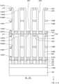
도 8은 예시적인 실시예들에 따른 집적회로 장치(100E)의 일부 구성을 나타내는 평면도들이다. 도 8의 좌측도는 제1 수직 레벨(LV1)에서의 평면도이고, 도 8의 우측도는 제2 수직 레벨(LV2)에서의 평면도이다. 도 9a는 도 8의 도 A2-A2' 선에 따른 단면도이고, 도 9b는 도 8의 도 B2-B2' 선에 따른 단면도이다. 도 8 내지 도 9b에서, 도 1 내지 도 7에서와 동일한 참조부호는 동일한 구성요소를 의미한다.FIG. 8 is a plan view showing a part of the configuration of an integrated circuit device (100E) according to exemplary embodiments. The left side of FIG. 8 is a plan view at a first vertical level (LV1), and the right side of FIG. 8 is a plan view at a second vertical level (LV2). FIG. 9a is a cross-sectional view taken along line A2-A2' of FIG. 8, and FIG. 9b is a cross-sectional view taken along line B2-B2' of FIG. 8. In FIGS. 8 to 9b, the same reference numerals as in FIGS. 1 to 7 denote the same components.
도 8 내지 도 9b를 참조하면, 제1 하부 전극(140E)은 제1 하부 전극부(142E) 및 제2 하부 전극부(144E)를 포함한다. 제1 하부 전극부(142E)는 제1 탑 영역(142T)에서 도 3b에서 설명된 것과 같은 경사면(142XS)을 포함하지 않으며, 제2 하부 전극부(144E)는 제2 탑 영역(144T)에서 경사면(144XS)을 포함할 수 있다.Referring to FIGS. 8 to 9B, the first lower electrode (140E) includes a first lower electrode portion (142E) and a second lower electrode portion (144E). The first lower electrode portion (142E) does not include an inclined surface (142XS) as described in FIG. 3B in the first top region (142T), and the second lower electrode portion (144E) may include an inclined surface (144XS) in the second top region (144T).
제1 탑 지지 패턴(152T)은 제1 몰드 개구부(OP1)를 정의하고 제1 몰드 개구부(OP1)에 의해 노출되는 제1 하부 전극부(142E)의 측벽은 제2 하부 전극부(144E)의 바닥부에 대하여 외측으로 돌출할 수 있다. 제2 탑 지지 패턴(154T)은 제2 몰드 개구부(OP2)를 정의하고 제2 몰드 개구부(OP2)에 의해 노출되는 제2 하부 전극부(144E)의 측벽에 경사면(144XS)이 배치될 수 있다.The first top support pattern (152T) defines a first mold opening (OP1), and a side wall of the first lower electrode portion (142E) exposed by the first mold opening (OP1) can protrude outwardly with respect to a bottom of the second lower electrode portion (144E). The second top support pattern (154T) defines a second mold opening (OP2), and an inclined surface (144XS) can be arranged on a side wall of the second lower electrode portion (144E) exposed by the second mold opening (OP2).
예시적인 제조 공정에 따르면, 제1 몰드 스택(MS1)(도 29 참조) 내의 제1 개구부(MSH1)(도 29 참조) 내에 제1 하부 전극부(142E)를 형성하고, 이후 제2 몰드 스택(MS2)(도 31a 참조) 내의 제2 개구부(MSH2)(도 31a 참조) 내에 제2 하부 전극부(144E)를 형성할 수 있다. 이후 마스크 패턴(252)(도 31a 참조)을 사용하여 제2 탑 지지 패턴(154T) 및 제2 중간 지지 패턴(154M)을 식각하여 제2 몰드 개구부(OP2)를 형성하고, 이후 제2 몰드 개구부(OP2)에 의해 노출되는 제1 탑 지지 패턴(152T) 및 제1 중간 지지 패턴(152M)을 식각하여 제1 몰드 개구부(OP1)를 형성할 수 있다. 이후, 제2 몰드 개구부(OP2)에 의해 노출된 제2 하부 전극부(144E)의 제2 탑 영역(144T)의 노출 부분을 트리밍하는 공정에 의해 경사면(144XS)이 형성될 수 있다.According to an exemplary manufacturing process, a first lower electrode portion (142E) may be formed in a first opening (MSH1) (see FIG. 29) in a first mold stack (MS1) (see FIG. 29), and then a second lower electrode portion (144E) may be formed in a second opening (MSH2) (see FIG. 31a) in a second mold stack (MS2) (see FIG. 31a). Then, a second top support pattern (154T) and a second middle support pattern (154M) may be etched using a mask pattern (252) (see FIG. 31a) to form a second mold opening (OP2), and then the first top support pattern (152T) and the first middle support pattern (152M) exposed by the second mold opening (OP2) may be etched to form a first mold opening (OP1). Thereafter, an inclined surface (144XS) can be formed by a process of trimming the exposed portion of the second top region (144T) of the second lower electrode portion (144E) exposed by the second mold opening (OP2).
도 8에 도시된 것과 같이, 제1 수직 레벨(LV1)에서 제1 하부 전극부(142E)의 수평 단면은 원형을 가질 수 있고, 제2 수직 레벨(LV2)에서 제2 하부 전극부(144E)의 수평 단면은 경사면(144XS)에 의해 정의되는, 원형이 아닌 일부분을 포함할 수 있다.As illustrated in FIG. 8, the horizontal cross-section of the first lower electrode portion (142E) at the first vertical level (LV1) may have a circular shape, and the horizontal cross-section of the second lower electrode portion (144E) at the second vertical level (LV2) may include a non-circular portion defined by the inclined plane (144XS).
도 10은 예시적인 실시예들에 따른 집적회로 장치(100F)를 나타내는 단면도이다. 도 10은 도 2의 A1-A1' 단면에 대응되는 단면을 나타낸다. 도 10에서, 도 1 내지 도 9b에서와 동일한 참조부호는 동일한 구성요소를 의미한다.Fig. 10 is a cross-sectional view showing an integrated circuit device (100F) according to exemplary embodiments. Fig. 10 shows a cross-section corresponding to the A1-A1' cross-section of Fig. 2. In Fig. 10, the same reference numerals as in Figs. 1 to 9b denote the same components.
도 10을 참조하면, 하부 전극(140F)은 제1 하부 전극부(142)와 제2 하부 전극부(144F)를 포함할 수 있고, 제1 하부 전극부(142)의 수직 방향에 따른 제1 높이(h11)보다 제2 하부 전극부(144F)의 수직 방향에 따른 제2 높이(h12)가 더 작을 수 있다. 예를 들어, 제2 높이(h12)는 제1 높이(h11)의 약 30% 내지 약 60%일 수 있으나 이에 한정되는 것은 아니다.Referring to FIG. 10, the lower electrode (140F) may include a first lower electrode portion (142) and a second lower electrode portion (144F), and a second height (h12) of the second lower electrode portion (144F) in the vertical direction may be smaller than a first height (h11) of the first lower electrode portion (142) in the vertical direction. For example, the second height (h12) may be about 30% to about 60% of the first height (h11), but is not limited thereto.
제2 하부 전극부(144F)의 제2 탑 영역(144T) 주위에 제2 탑 지지 패턴(154T)이 배치되고, 제2 탑 지지 패턴(154T)의 상면은 도 3a에 기재된 제2 수직 레벨(LV2)(도 3a 참조)보다 더 낮은 제3 수직 레벨(LV3)에 배치될 수 있다. 제2 하부 전극부(144F)의 제2 메인 영역(144M) 측벽 상에 도 3a에서 설명된 제2 중간 지지 패턴(154M)이 형성되지 않을 수 있다. 이에 따라 제2 하부 전극부(144F)의 제2 메인 영역(144M)은 제2 중간 지지 패턴(154M)에 의해 둘러싸이는 제3 돌출부(144P1)(도 3a 참조)를 포함하지 않을 수 있다.A second top support pattern (154T) is arranged around a second top region (144T) of a second lower electrode portion (144F), and an upper surface of the second top support pattern (154T) may be arranged at a third vertical level (LV3) lower than the second vertical level (LV2) (see FIG. 3A) described in FIG. 3A. The second middle support pattern (154M) described in FIG. 3A may not be formed on a sidewall of the second main region (144M) of the second lower electrode portion (144F). Accordingly, the second main region (144M) of the second lower electrode portion (144F) may not include a third protrusion (144P1) (see FIG. 3A) surrounded by the second middle support pattern (154M).
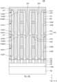
도 11 내지 도 24b는 예시적인 실시예들에 따른 집적회로 장치(100)의 제조 방법을 공정 순서에 따라 나타내는 단면도들이다. 구체적으로, 도 11 내지 13, 14a, 15a, 16a, 17 내지 20, 21a, 22a, 23a, 및 24a는 도 2의 A1-A1' 선을 따른 단면에 대응하는 단면들을 나타내며, 도 14b, 15b, 16b, 21b, 22b, 23b, 및 24b는 도 2의 B1-B1' 선을 따른 단면에 대응하는 단면들을 나타낸다.FIGS. 11 to 24b are cross-sectional views showing a manufacturing method of an integrated circuit device (100) according to exemplary embodiments in a process sequence. Specifically, FIGS. 11 to 13, 14a, 15a, 16a, 17 to 20, 21a, 22a, 23a, and 24a show cross-sections corresponding to cross-sections taken along line A1-A1' of FIG. 2, and FIGS. 14b, 15b, 16b, 21b, 22b, 23b, and 24b show cross-sections corresponding to cross-sections taken along line B1-B1' of FIG.
도 11을 참조하면, 기판(110)의 상면(110M) 상에 하부 구조물(120)을 형성하고, 하부 구조물(120) 상에 랜딩 패드(130)와, 랜딩 패드(130)의 측벽을 둘러싸는 노드 분리 절연층(132)을 형성할 수 있다.Referring to FIG. 11, a lower structure (120) can be formed on the upper surface (110M) of a substrate (110), and a landing pad (130) and a node separation insulating layer (132) surrounding the side wall of the landing pad (130) can be formed on the lower structure (120).
이후, 랜딩 패드(130)와 노드 분리 절연층(132) 상에 식각 정지층(134) 및 제1 몰드 스택(MS1)을 순서대로 형성할 수 있다. 제1 몰드 스택(MS1)은 식각 정지층(134) 상에 순차적으로 적층되는 제1 몰드층(212), 제1 중간 지지 패턴(152M), 제2 몰드층(214), 및 제1 탑 지지 패턴(152T)을 포함할 수 있다.Thereafter, an etching stop layer (134) and a first mold stack (MS1) can be sequentially formed on the landing pad (130) and the node separation insulating layer (132). The first mold stack (MS1) can include a first mold layer (212), a first intermediate support pattern (152M), a second mold layer (214), and a first top support pattern (152T) that are sequentially stacked on the etching stop layer (134).
예시적인 실시예들에 있어서, 제1 몰드층(212)과 식각 정지층(134)은 서로에 대하여 식각 선택비를 갖는 물질들을 포함할 수 있다. 예를 들어 제1 몰드층(212)이 실리콘 산화물을 포함하는 경우, 식각 정지층(134)은 실리콘 질화물, 실리콘 산질화물, 또는 실리콘 카본 질화물(SiCN)을 포함할 수 있다. 또한 제1 및 제2 몰드층(212, 214)과 제1 중간 지지 패턴(152M)은 서로에 대하여 식각 선택비를 갖는 물질들을 포함할 수 있고, 제1 및 제2 몰드층(212, 214)과 제1 탑 지지 패턴(152T)은 서로에 대하여 식각 선택비를 갖는 물질들을 포함할 수 있다. 예를 들어 제1 및 제2 몰드층(212, 214)이 실리콘 산화물을 포함하는 경우, 제1 중간 지지 패턴(152M)과 제1 탑 지지 패턴(152T)은 실리콘 질화물, 실리콘 산질화물, 실리콘 보론 질화물(SiBN), 또는 실리콘 카본 질화물(SiCN)을 포함할 수 있다.In exemplary embodiments, the first mold layer (212) and the etch stop layer (134) may include materials having an etch selectivity with respect to each other. For example, when the first mold layer (212) includes silicon oxide, the etch stop layer (134) may include silicon nitride, silicon oxynitride, or silicon carbon nitride (SiCN). In addition, the first and second mold layers (212, 214) and the first intermediate support pattern (152M) may include materials having an etch selectivity with respect to each other, and the first and second mold layers (212, 214) and the first top support pattern (152T) may include materials having an etch selectivity with respect to each other. For example, when the first and second mold layers (212, 214) include silicon oxide, the first intermediate support pattern (152M) and the first top support pattern (152T) may include silicon nitride, silicon oxynitride, silicon boron nitride (SiBN), or silicon carbon nitride (SiCN).
도 12를 참조하면, 제1 탑 지지 패턴(152T) 상에 개구부(222H)를 구비하는 제1 마스크 패턴(222)을 형성하고, 제1 마스크 패턴(222)을 사용하여 제1 몰드 스택(MS1)을 관통하는 개구부(MSH1)를 형성할 수 있다.Referring to FIG. 12, a first mask pattern (222) having an opening (222H) is formed on a first top support pattern (152T), and an opening (MSH1) penetrating a first mold stack (MS1) can be formed using the first mask pattern (222).
예시적인 실시예들에서, 제1 마스크 패턴(222)은 폴리실리콘, 실리콘 질화물, 실리콘 산화물, 실리콘 산질화물, SOH(spin-on-hardmask), ACL(amorphous carbon layer), 또는 이들의 조합일 수 있다.In exemplary embodiments, the first mask pattern (222) can be polysilicon, silicon nitride, silicon oxide, silicon oxynitride, spin-on-hardmask (SOH), amorphous carbon layer (ACL), or a combination thereof.
개구부(MSH1)는 제1 몰드 스택(MS1)을 관통하도록 제3 방향(Z 방향)으로 연장될 수 있고, 개구부(MSH1) 중 제1 탑 지지 패턴(152T)을 관통하는 일부분이 제1 개구부(152TH)로, 개구부(MSH1) 중 제1 중간 지지 패턴(152M)을 관통하는 일부분이 제2 개구부(152MH)로 지칭될 수 있다. 개구부(MSH1)의 형성 후에, 식각 정지층(134)의 일부분이 제거되고, 식각 정지층(134)에 개구부(MSH1)와 연결되는 개구부(134H)가 형성될 수 있다. 개구부(MSH1) 및 개구부(134H)에 의해 랜딩 패드(130)의 상면이 노출될 수 있다.The opening (MSH1) can extend in a third direction (Z direction) to penetrate the first mold stack (MS1), and a portion of the opening (MSH1) penetrating the first top support pattern (152T) can be referred to as a first opening (152TH), and a portion of the opening (MSH1) penetrating the first middle support pattern (152M) can be referred to as a second opening (152MH). After the formation of the opening (MSH1), a portion of the etch stop layer (134) can be removed, and an opening (134H) connected to the etch stop layer (134) can be formed. An upper surface of the landing pad (130) can be exposed by the opening (MSH1) and the opening (134H).
도 13을 참조하면, 랜딩 패드(130) 및 제1 몰드 스택(MS1) 상에 도전층을 사용하여 개구부(134H, MSH1)의 내부를 채우고, 제1 탑 지지 패턴(152T)의 상면이 노출될 때까지 상기 도전층 상부를 제거하여 제1 하부 전극부(142)를 형성할 수 있다.Referring to FIG. 13, a conductive layer may be used on the landing pad (130) and the first mold stack (MS1) to fill the interior of the opening (134H, MSH1), and the upper portion of the conductive layer may be removed until the upper surface of the first top support pattern (152T) is exposed, thereby forming the first lower electrode portion (142).
예를 들어, 제1 하부 전극부(142)의 형성 공정은 화학 기상 증착(chemical vapor deposition, CVD) 공정, 금속 유기 CVD (MOCVD) 공정, 원자층 증착(atomic layer deposition, ALD) 공정, 또는 금속 유기 ALD (MOALD) 공정일 수 있다.For example, the formation process of the first lower electrode portion (142) may be a chemical vapor deposition (CVD) process, a metal organic CVD (MOCVD) process, an atomic layer deposition (ALD) process, or a metal organic ALD (MOALD) process.
도 14a 및 도 14b를 참조하면, 제1 하부 전극부(142)와 제1 몰드 스택(MS1) 상에 개구부(224H)를 포함하는 제2 마스크 패턴(224)을 형성할 수 있다. 이후 제2 마스크 패턴(224)을 식각 마스크로 사용하여 제1 탑 지지 패턴(152T), 제2 몰드층(214) 및 제1 중간 지지 패턴(152M)의 일부분을 제거하여 제1 몰드 개구부(OP1)를 형성할 수 있다. 이 때 제1 몰드 개구부(OP1)는 제1 하부 전극부(142)의 상면 일부분 및 측벽 일부분을 노출하도록 형성될 수 있다.Referring to FIGS. 14A and 14B, a second mask pattern (224) including an opening (224H) may be formed on the first lower electrode portion (142) and the first mold stack (MS1). Thereafter, the second mask pattern (224) may be used as an etching mask to remove a portion of the first top support pattern (152T), the second mold layer (214), and the first middle support pattern (152M), thereby forming a first mold opening (OP1). At this time, the first mold opening (OP1) may be formed to expose a portion of the upper surface and a portion of the sidewall of the first lower electrode portion (142).
이후, 제1 몰드 개구부(OP1)에 의해 노출되는 제1 하부 전극부(142)의 상측 상에 트리밍 공정을 수행하여, 제1 하부 전극부(142)의 상측에 경사면(142XS)을 형성할 수 있다.Thereafter, a trimming process may be performed on the upper side of the first lower electrode portion (142) exposed by the first mold opening (OP1) to form an inclined surface (142XS) on the upper side of the first lower electrode portion (142).
도 15a 및 도 15b를 참조하면, 제2 몰드층(214)을 제거하고 제1 몰드층(212)의 일부분을 제거하여 제1 몰드층 잔류부(212R)를 형성할 수 있다.Referring to FIGS. 15a and 15b, the second mold layer (214) can be removed and a portion of the first mold layer (212) can be removed to form a first mold layer residual portion (212R).
예시적인 실시예들에서, 제1 몰드층(212)의 일부분 및 제2 몰드층(214)의 제거 공정은 불화암모늄(NH4F), 불산(HF) 및 물을 포함하는 식각제를 사용한 식각 공정일 수 있다.In exemplary embodiments, the removal process of a portion of the first mold layer (212) and the second mold layer (214) may be an etching process using an etchant including ammonium fluoride (NH4 F), hydrofluoric acid (HF), and water.
제1 몰드층(212)의 일부분 및 제2 몰드층(214)을 제거하기 위한 공정에서, 제1 탑 지지 패턴(152T) 및 제1 중간 지지 패턴(152M)은 제거되지 않을 수 있고, 인접한 두 개의 제1 하부 전극부(142)가 제1 탑 지지 패턴(152T) 및 제1 중간 지지 패턴(152M)에 연결되고 이들에 의해 지지될 수 있다. 또한 제1 몰드층(212)의 일부분이 제거된 후 제1 몰드층 잔류부(212R)는 제1 하부 전극부(142)의 측벽 하측을 둘러쌀 수 있다.In a process for removing a portion of the first mold layer (212) and the second mold layer (214), the first top support pattern (152T) and the first middle support pattern (152M) may not be removed, and two adjacent first lower electrode parts (142) may be connected to and supported by the first top support pattern (152T) and the first middle support pattern (152M). In addition, after a portion of the first mold layer (212) is removed, the first mold layer residual portion (212R) may surround the lower side of the side wall of the first lower electrode part (142).
도 16a 및 도 16b를 참조하면, 제1 하부 전극부(142)의 노출된 부분에 제1 트리밍 공정을 수행하여 제1 하부 전극부(142)의 수평 방향 폭을 감소시킬 수 있다.Referring to FIGS. 16a and 16b, a first trimming process can be performed on an exposed portion of the first lower electrode portion (142) to reduce the horizontal width of the first lower electrode portion (142).
예시적인 실시예들에서, 상기 제1 트리밍 공정은 등방성의 건식 식각 또는 습식 식각 공정을 포함할 수 있다. 예를 들어, 상기 제1 트리밍 공정이 습식 식각을 포함하는 경우, 상기 제1 트리밍 공정은 인산, 질산, 초산, 또는 이들의 조합을 포함하는 식각제를 이용하여 수행될 수 있다.In exemplary embodiments, the first trimming process may include an isotropic dry etching or wet etching process. For example, when the first trimming process includes wet etching, the first trimming process may be performed using an etchant including phosphoric acid, nitric acid, acetic acid, or a combination thereof.
예시적인 실시예들에서, 상기 제1 트리밍 공정은, 상기 제1 트리밍 공정 이후에 제1 하부 전극부(142)의 수평 치수가 식각 전의 상기 제1 트리밍 공정 이전의 수평 치수의 약 60% 내지 약 90%가 되도록 수행될 수 있다.In exemplary embodiments, the first trimming process may be performed such that the horizontal dimension of the first lower electrode portion (142) after the first trimming process is about 60% to about 90% of the horizontal dimension before the first trimming process and before etching.
제1 중간 지지 패턴(152M)에 의해 둘러싸이는 제1 하부 전극부(142)의 측벽 일부분과 제1 탑 지지 패턴(152T)에 의해 둘러싸이는 제1 하부 전극부(142)의 제1 탑 영역(142T)은 상기 제1 트리밍 공정에 의해 수평 방향 폭이 감소되지 않을 수 있고, 이에 따라 제1 중간 지지 패턴(152M)에 접하는 제1 돌출부(142P1)와 제1 탑 지지 패턴(152T)에 접하는 제2 돌출부(142P2)가 형성될 수 있다. 또한 제1 몰드층 잔류부(212R)에 의해 커버되는 제1 하부 전극부(142)의 측벽 또한 상기 제1 트리밍 공정에 의해 수평 방향 폭이 감소되지 않을 수 있고, 제1 몰드층 잔류부(212R)의 상면과 동일한 수직 레벨에서 단차부(142ST)가 형성될 수 있다.A portion of the sidewall of the first lower electrode portion (142) surrounded by the first intermediate support pattern (152M) and a first top region (142T) of the first lower electrode portion (142) surrounded by the first top support pattern (152T) may not have a horizontal width reduced by the first trimming process, and thus a first protrusion (142P1) in contact with the first intermediate support pattern (152M) and a second protrusion (142P2) in contact with the first top support pattern (152T) may be formed. In addition, a sidewall of the first lower electrode portion (142) covered by the first mold layer residual portion (212R) may also not have a horizontal width reduced by the first trimming process, and a step portion (142ST) may be formed at the same vertical level as an upper surface of the first mold layer residual portion (212R).
도 17을 참조하면, 제1 탑 지지 패턴(152T) 및 제1 중간 지지 패턴(152M)을 커버하고 복수의 제1 하부 전극부(142) 사이의 공간을 채우는 보호층(230)을 형성하고, 제1 탑 지지 패턴(152T)의 상면이 노출될 때까지 보호층(230)의 상면을 에치백할 수 있다.Referring to FIG. 17, a protective layer (230) covering the first top support pattern (152T) and the first middle support pattern (152M) and filling the space between the plurality of first lower electrode portions (142) may be formed, and the upper surface of the protective layer (230) may be etched back until the upper surface of the first top support pattern (152T) is exposed.
예시적인 실시예들에서, 보호층(230)은 실리콘 산화물, 실리콘 산질화물, SOH(spin-on-hardmask), ACL(amorphous carbon layer) 중 적어도 하나를 포함할 수 있다.In exemplary embodiments, the protective layer (230) may include at least one of silicon oxide, silicon oxynitride, spin-on-hardmask (SOH), and amorphous carbon layer (ACL).
도 18을 참조하면, 제1 하부 전극부(142) 및 제1 탑 지지 패턴(152T) 상에 제2 몰드 스택(MS2)을 형성할 수 있다. 제2 몰드 스택(MS2)은 제3 몰드층(242), 제2 중간 지지 패턴(154M), 제4 몰드층(244), 및 제2 탑 지지 패턴(154T)을 포함할 수 있다.Referring to FIG. 18, a second mold stack (MS2) may be formed on the first lower electrode portion (142) and the first top support pattern (152T). The second mold stack (MS2) may include a third mold layer (242), a second middle support pattern (154M), a fourth mold layer (244), and a second top support pattern (154T).
예시적인 실시예들에서, 제3 및 제4 몰드층(242, 244)과 제2 중간 지지 패턴(154M)은 서로에 대하여 식각 선택비를 갖는 물질들을 포함할 수 있고, 제3 및 제4 몰드층(242, 244)과 제2 탑 지지 패턴(154T)은 서로에 대하여 식각 선택비를 갖는 물질들을 포함할 수 있다. 예를 들어 제3 및 제4 몰드층(242, 244)이 실리콘 산화물을 포함하는 경우, 제2 중간 지지 패턴(154M)과 제2 탑 지지 패턴(154T)은 실리콘 질화물, 실리콘 산질화물, 실리콘 보론 질화물(SiBN), 또는 실리콘 카본 질화물(SiCN)을 포함할 수 있다.In exemplary embodiments, the third and fourth mold layers (242, 244) and the second intermediate support pattern (154M) may include materials having an etch selectivity with respect to each other, and the third and fourth mold layers (242, 244) and the second top support pattern (154T) may include materials having an etch selectivity with respect to each other. For example, when the third and fourth mold layers (242, 244) include silicon oxide, the second intermediate support pattern (154M) and the second top support pattern (154T) may include silicon nitride, silicon oxynitride, silicon boron nitride (SiBN), or silicon carbon nitride (SiCN).
도 19를 참조하면, 제2 탑 지지 패턴(154T) 상에 개구부(252H)를 구비하는 제3 마스크 패턴(252)을 형성하고, 제3 마스크 패턴(252)을 사용하여 제2 몰드 스택(MS2)을 관통하는 개구부(MSH2)를 형성할 수 있다.Referring to FIG. 19, a third mask pattern (252) having an opening (252H) may be formed on a second tower support pattern (154T), and an opening (MSH2) penetrating a second mold stack (MS2) may be formed using the third mask pattern (252).
예시적인 실시예들에서, 제3 마스크 패턴(252)은 폴리실리콘, 실리콘 질화물, 실리콘 산화물, 실리콘 산질화물, SOH, ACL, 또는 이들의 조합일 수 있다.In exemplary embodiments, the third mask pattern (252) can be polysilicon, silicon nitride, silicon oxide, silicon oxynitride, SOH, ACL, or a combination thereof.
개구부(MSH2)는 제2 몰드 스택(MS2)을 관통하도록 제3 방향(Z 방향)으로 연장될 수 있고, 개구부(MSH2) 중 제2 탑 지지 패턴(154T)을 관통하는 일부분이 제3 개구부(154TH)로, 개구부(MSH2) 중 제2 중간 지지 패턴(154M)을 관통하는 일부분이 제4 개구부(154MH)로 지칭될 수 있다. 개구부(MSH2)의 바닥부에 제1 하부 전극부(142)의 상면이 노출될 수 있다.The opening (MSH2) may extend in a third direction (Z direction) to penetrate the second mold stack (MS2), and a portion of the opening (MSH2) penetrating the second top support pattern (154T) may be referred to as a third opening (154TH), and a portion of the opening (MSH2) penetrating the second middle support pattern (154M) may be referred to as a fourth opening (154MH). An upper surface of the first lower electrode portion (142) may be exposed at a bottom portion of the opening (MSH2).
도 20을 참조하면, 제2 몰드 스택(MS2) 상에 도전층을 사용하여 개구부(MSH2)의 내부를 채우고, 제2 탑 지지 패턴(154T)의 상면이 노출될 때까지 상기 도전층 상부를 제거하여 제2 하부 전극부(144)를 형성할 수 있다.Referring to FIG. 20, a conductive layer may be used on a second mold stack (MS2) to fill the interior of the opening (MSH2), and an upper portion of the conductive layer may be removed until the upper surface of the second top support pattern (154T) is exposed to form a second lower electrode portion (144).
도 21a 및 도 21b를 참조하면, 제2 하부 전극부(144)와 제2 몰드 스택(MS2) 상에 개구부(254H)를 포함하는 제4 마스크 패턴(254)을 형성할 수 있다. 이후 제4 마스크 패턴(254)을 식각 마스크로 사용하여 제2 탑 지지 패턴(154T), 제4 몰드층(244) 및 제2 중간 지지 패턴(154M)의 일부분을 제거하여 제2 몰드 개구부(OP2)를 형성할 수 있다. 이 때 제2 몰드 개구부(OP2)는 제2 하부 전극부(144)의 상면 일부분 및 측벽 일부분을 노출하도록 형성될 수 있다.Referring to FIGS. 21A and 21B, a fourth mask pattern (254) including an opening (254H) may be formed on the second lower electrode portion (144) and the second mold stack (MS2). Thereafter, the fourth mask pattern (254) may be used as an etching mask to remove a portion of the second top support pattern (154T), the fourth mold layer (244), and the second middle support pattern (154M), thereby forming a second mold opening (OP2). At this time, the second mold opening (OP2) may be formed to expose a portion of the upper surface and a portion of the sidewall of the second lower electrode portion (144).
이후, 제2 몰드 개구부(OP2)에 의해 노출되는 제2 하부 전극부(144)의 상측 상에 트리밍 공정을 수행하여, 제2 하부 전극부(144)의 상측에 경사면(144XS)을 형성할 수 있다.Thereafter, a trimming process may be performed on the upper side of the second lower electrode portion (144) exposed by the second mold opening (OP2) to form an inclined surface (144XS) on the upper side of the second lower electrode portion (144).
도 22a 및 도 22b를 참조하면, 제4 몰드층(244)을 제거하고 제3 몰드층(242)의 일부분을 제거하여 제3 몰드층 잔류부(242R)를 형성할 수 있다.Referring to FIGS. 22a and 22b, the fourth mold layer (244) can be removed and a portion of the third mold layer (242) can be removed to form a third mold layer residual portion (242R).
예시적인 실시예들에서, 제3 몰드층(242)의 일부분 및 제4 몰드층(244)의 제거 공정은 불화암모늄(NH4F), 불산(HF) 및 물을 포함하는 식각제를 사용한 식각 공정일 수 있다. 제3 몰드층(242)의 일부분이 제거된 후 제3 몰드층 잔류부(242R)는 제2 하부 전극부(144)의 측벽 하측을 둘러쌀 수 있다.In exemplary embodiments, the removal process of a portion of the third mold layer (242) and the fourth mold layer (244) may be an etching process using an etchant including ammonium fluoride (NH4 F), hydrofluoric acid (HF), and water. After a portion of the third mold layer (242) is removed, the third mold layer residue (242R) may surround the lower side of the sidewall of the second lower electrode portion (144).
이후, 제2 하부 전극부(144)의 노출된 부분에 제2 트리밍 공정을 수행하여 제2 하부 전극부(144)의 수평 방향 폭을 감소시킬 수 있다.Thereafter, a second trimming process can be performed on the exposed portion of the second lower electrode portion (144) to reduce the horizontal width of the second lower electrode portion (144).
예시적인 실시예들에서, 상기 제2 트리밍 공정은 등방성의 건식 식각 또는 습식 식각 공정을 포함할 수 있다. 예를 들어, 상기 제2 트리밍 공정이 습식 식각을 포함하는 경우, 상기 제2 트리밍 공정은 인산, 질산, 초산, 또는 이들의 조합을 포함하는 식각제를 이용하여 수행될 수 있다.In exemplary embodiments, the second trimming process may include an isotropic dry etching or wet etching process. For example, when the second trimming process includes wet etching, the second trimming process may be performed using an etchant including phosphoric acid, nitric acid, acetic acid, or a combination thereof.
제2 중간 지지 패턴(154M)에 의해 둘러싸이는 제2 하부 전극부(144)의 측벽 일부분과 제2 탑 지지 패턴(154T)에 의해 둘러싸이는 제2 하부 전극부(144)의 제2 탑 영역(144T)은 상기 제2 트리밍 공정에 의해 수평 방향 폭이 감소되지 않을 수 있고, 이에 따라 제2 중간 지지 패턴(154M)에 접하는 제3 돌출부(144P1)와 제2 탑 지지 패턴(154T)에 접하는 제4 돌출부(144P2)가 형성될 수 있다. 또한 제3 몰드층 잔류부(242R)에 의해 커버되는 제2 하부 전극부(144)의 측벽 또한 상기 제1 트리밍 공정에 의해 수평 방향 폭이 감소되지 않을 수 있고, 제3 몰드층 잔류부(242R)의 상면과 동일한 수직 레벨에서 단차부(144ST)가 형성될 수 있다.A portion of the sidewall of the second lower electrode portion (144) surrounded by the second intermediate support pattern (154M) and a second top region (144T) of the second lower electrode portion (144) surrounded by the second top support pattern (154T) may not have a horizontal width reduced by the second trimming process, and thus a third protrusion (144P1) in contact with the second intermediate support pattern (154M) and a fourth protrusion (144P2) in contact with the second top support pattern (154T) may be formed. In addition, a sidewall of the second lower electrode portion (144) covered by the third mold layer residual portion (242R) may also not have a horizontal width reduced by the first trimming process, and a step portion (144ST) may be formed at the same vertical level as an upper surface of the third mold layer residual portion (242R).
도 23a 및 도 23b를 참조하면, 제3 몰드층 잔류부(242R)(도 22a 참조), 보호층(230)(도 22a 참조), 및 제1 몰드층 잔류부(212R)(도 22a 참조)를 제거할 수 있다.Referring to FIGS. 23a and 23b, the third mold layer residual portion (242R) (see FIG. 22a), the protective layer (230) (see FIG. 22a), and the first mold layer residual portion (212R) (see FIG. 22a) can be removed.
도 24a 및 도 24b를 참조하면, 제1 하부 전극부(142) 및 제2 하부 전극부(144)의 노출된 표면에 유전층(160)을 콘포말하게 형성할 수 있다. 이 때, 제1 중간 지지 패턴(152M), 제1 탑 지지 패턴(152T), 제2 중간 지지 패턴(154M), 및, 제2 탑 지지 패턴(154T)의 노출된 표면에도 유전층(160)이 형성될 수 있다. 제1 하부 전극부(142)의 표면 중 제1 중간 지지 패턴(152M) 및 제1 탑 지지 패턴(152T)과 접촉하는 부분과, 제2 하부 전극부(144)의 표면 중 제2 중간 지지 패턴(154M) 및 제2 탑 지지 패턴(154T)과 접촉하는 부분에는 유전층(160)이 형성되지 않을 수 있다.Referring to FIGS. 24a and 24b, a dielectric layer (160) can be conformally formed on the exposed surfaces of the first lower electrode portion (142) and the second lower electrode portion (144). At this time, the dielectric layer (160) can also be formed on the exposed surfaces of the first intermediate support pattern (152M), the first top support pattern (152T), the second intermediate support pattern (154M), and the second top support pattern (154T). The dielectric layer (160) may not be formed on a portion of the surface of the first lower electrode portion (142) that is in contact with the first intermediate support pattern (152M) and the first top support pattern (152T), and a portion of the surface of the second lower electrode portion (144) that is in contact with the second intermediate support pattern (154M) and the second top support pattern (154T).
이후 유전층(160)을 커버하는 상부 전극(170)을 형성할 수 있다.Afterwards, an upper electrode (170) covering the dielectric layer (160) can be formed.
선택적으로, 상부 전극(170)을 형성한 후에 어닐링 처리가 더 수행될 수 있다.Optionally, annealing treatment may be further performed after forming the upper electrode (170).
전술한 예시적인 실시예들에 따른 집적회로 장치(100)의 제조 방법에 따르면, 제1 하부 전극부(142)의 측벽의 폭을 감소시키기 위한 트리밍 공정과 제2 하부 전극부(144)의 측벽의 폭을 감소시키기 위한 트리밍 공정이 수행될 수 있고, 제1 하부 전극부(142)와 제2 하부 전극부(144)는 이에 인접한 제1 하부 전극부(142)와 제2 하부 전극부(144)와의 충분한 이격거리가 확보될 수 있다. 이에 따라 하부 전극(140)은 증가된 높이를 갖는 한편 하부 전극(140)의 브릿지 불량의 발생 또는 누설 전류의 발생이 방지될 수 있다. 상기 집적회로 장치(100)는 우수한 전기적 특성을 가질 수 있다.According to the method for manufacturing the integrated circuit device (100) according to the exemplary embodiments described above, a trimming process for reducing the width of the sidewall of the first lower electrode portion (142) and a trimming process for reducing the width of the sidewall of the second lower electrode portion (144) can be performed, and a sufficient separation distance between the first lower electrode portion (142) and the second lower electrode portion (144) adjacent thereto can be secured. Accordingly, the lower electrode (140) can have an increased height, while occurrence of a bridge failure of the lower electrode (140) or occurrence of a leakage current can be prevented. The integrated circuit device (100) can have excellent electrical characteristics.
한편, 도 15a 및 도 15b에서는 제1 몰드층(212)의 일부분과 제2 몰드층(214)이 제거되고 제1 몰드층 잔류부(212R)가 제1 중간 지지 패턴(152M)의 바닥면보다 낮은 레벨에 배치되고 제1 하부 전극부(142)의 측벽 하측만을 둘러싸는 상대적으로 작은 높이로 형성되는 것이 예시적으로 설명되었다. 마찬가지로, 도 22a 및 도 22b에서는 제3 몰드층(242)의 일부분과 제4 몰드층(244)이 제거되고 제3 몰드층 잔류부(242R)가 제2 중간 지지 패턴(154M)의 바닥면보다 낮은 레벨에 배치되고 제2 하부 전극부(144)의 측벽 하측만을 둘러싸는 상대적으로 작은 높이로 형성되는 것이 예시적으로 설명되었다.Meanwhile, in FIGS. 15A and 15B, it is exemplarily explained that a part of the first mold layer (212) and the second mold layer (214) are removed, and the first mold layer residual portion (212R) is formed at a level lower than the bottom surface of the first intermediate support pattern (152M) and has a relatively small height surrounding only the lower side of the side wall of the first lower electrode portion (142). Similarly, in FIGS. 22A and 22B, it is exemplarily explained that a part of the third mold layer (242) and the fourth mold layer (244) are removed, and the third mold layer residual portion (242R) is formed at a level lower than the bottom surface of the second intermediate support pattern (154M) and has a relatively small height surrounding only the lower side of the side wall of the second lower electrode portion (144).
그러나 이와는 달리 제2 몰드층(214)만이 제거되고 제1 몰드층(212)이 제거되지 않을 수도 있다. 이러한 경우에, 제1 중간 지지 패턴(152M)의 상면보다 높은 레벨에 배치되는 제1 하부 전극부(142A)(도 4 참조)의 측벽 상측에 제1 트리밍 공정이 수행되어 제1 하부 전극부(142A)의 측벽 상측의 수평 방향 폭만이 감소될 수도 있다. 또한 제4 몰드층(244)만이 제거되고 제3 몰드층(242)이 제거되지 않을 수도 있다. 이러한 경우에, 제2 중간 지지 패턴(154M)의 상면보다 높은 레벨에 배치되는 제2 하부 전극부(144A)(도 4 참조)의 측벽 상측에 제2 트리밍 공정이 수행되어 제2 하부 전극부(144)의 측벽 상측의 수평 방향 폭만이 감소될 수도 있다. 이에 따라 도 4를 참조로 설명한 집적회로 장치(100A)가 형성될 수 있다.However, unlike this, only the second mold layer (214) may be removed and the first mold layer (212) may not be removed. In this case, the first trimming process may be performed on the upper side of the sidewall of the first lower electrode portion (142A) (see FIG. 4) which is arranged at a level higher than the upper surface of the first intermediate support pattern (152M) so that only the horizontal width of the upper side of the sidewall of the first lower electrode portion (142A) may be reduced. In addition, only the fourth mold layer (244) may be removed and the third mold layer (242) may not be removed. In this case, the second trimming process may be performed on the upper side of the sidewall of the second lower electrode portion (144A) (see FIG. 4) which is arranged at a level higher than the upper surface of the second intermediate support pattern (154M) so that only the horizontal width of the upper side of the sidewall of the second lower electrode portion (144) may be reduced. Accordingly, an integrated circuit device (100A) described with reference to FIG. 4 can be formed.
또한, 도 16a 및 도 16b에서는 제1 하부 전극부(142)의 수평 방향 폭을 감소시키기 위한 제1 트리밍 공정을 수행한 것이 예시적으로 설명되었다. 그러나 이와는 달리 제1 몰드 개구부(OP1)를 형성한 후에 제1 몰드층(212)의 일부분과 제2 몰드층(214)을 제거하는 공정이 수행되지 않을 수 있고, 제1 하부 전극부(142)의 수평 방향 폭을 감소시키기 위한 제1 트리밍 공정이 수행되지 않을 수도 있다. 이후 제1 몰드 개구부(OP1)가 형성된 제1 몰드 스택(MS1) 상에 제2 몰드 스택(MS2)이 형성되고, 도 19 내지 도 24b를 참조로 설명한 공정들이 수행될 수 있다. 이러한 경우에, 제1 하부 전극부(142B)는 그 전체 높이를 따라 일정한 기울기를 갖거나 연속적으로 연결되는 측벽을 가질 수 있고, 이에 따라 도 5a 및 도 5b를 참조로 설명한 집적회로 장치(100B)가 형성될 수 있다.In addition, in FIGS. 16A and 16B, it has been exemplarily described that the first trimming process for reducing the horizontal width of the first lower electrode portion (142) was performed. However, differently, the process of removing a part of the first mold layer (212) and the second mold layer (214) after forming the first mold opening (OP1) may not be performed, and the first trimming process for reducing the horizontal width of the first lower electrode portion (142) may not be performed. Thereafter, a second mold stack (MS2) is formed on the first mold stack (MS1) on which the first mold opening (OP1) is formed, and the processes described with reference to FIGS. 19 to 24B may be performed. In this case, the first lower electrode portion (142B) may have side walls that have a constant slope or are continuously connected along its entire height, and thus the integrated circuit device (100B) described with reference to FIGS. 5A and 5B may be formed.
또한, 도 13 및 도 20에서는 제1 하부 전극부(142)와 제2 하부 전극부(144)가 각각 제1 몰드 스택(MS1)의 개구부(MSH1)와 제2 몰드 스택(MS2)의 개구부(MSH2)를 완전히 채우는 필라 형상으로 형성되는 것이 예시적으로 설명되었다. 그러나 이와는 달리, 제1 하부 전극부(142)는 제1 몰드 스택(MS1)의 개구부(MSH1)를 완전히 채우지 않고 내부에 제1 심 영역(SR1)을 포함하도록 형성되고, 제2 하부 전극부(144)는 제2 몰드 스택(MS2)의 개구부(MSH2)를 완전히 채우지 않고 내부에 제2 심 영역(SR2)을 포함하도록 형성될 수도 있다. 이러한 경우에 도 7을 참조로 설명한 집적회로 장치(100D)가 형성될 수 있다.In addition, in FIG. 13 and FIG. 20, it is exemplarily explained that the first lower electrode part (142) and the second lower electrode part (144) are formed in a pillar shape that completely fills the opening (MSH1) of the first mold stack (MS1) and the opening (MSH2) of the second mold stack (MS2), respectively. However, differently from this, the first lower electrode part (142) may be formed so as to include the first core region (SR1) therein without completely filling the opening (MSH1) of the first mold stack (MS1), and the second lower electrode part (144) may be formed so as to include the second core region (SR2) therein without completely filling the opening (MSH2) of the second mold stack (MS2). In this case, the integrated circuit device (100D) described with reference to FIG. 7 may be formed.
또한 도 18에서 제2 몰드 스택(MS2)이 제3 몰드층(242)과 제2 중간 지지 패턴(154M)을 포함하는 것이 예시적으로 설명되었다. 그러나 이와는 달리 제2 몰드 스택(MS2)이 제4 몰드층(244)과 제2 탑 지지 패턴(154T)을 포함하고, 제4 몰드층(244)이 제1 하부 전극부(142)와 제1 탑 지지 패턴(152T) 직접 상부에 배치될 수도 있다. 이러한 경우에 도 10을 참조로 설명한 집적회로 장치(100F)가 형성될 수 있다.Also, in FIG. 18, it is exemplarily described that the second mold stack (MS2) includes the third mold layer (242) and the second middle support pattern (154M). However, differently, the second mold stack (MS2) may include the fourth mold layer (244) and the second top support pattern (154T), and the fourth mold layer (244) may be disposed directly on the first lower electrode portion (142) and the first top support pattern (152T). In this case, the integrated circuit device (100F) described with reference to FIG. 10 may be formed.
도 25 내지 도 28은 예시적인 실시예들에 따른 집적회로 장치(100C)의 제조 방법을 공정 순서에 따라 나타내는 단면도들이다.FIGS. 25 to 28 are cross-sectional views showing a manufacturing method of an integrated circuit device (100C) according to exemplary embodiments in the order of processes.
도 25를 참조하면, 제1 몰드 스택(MS1) 상에 개구부(222H)를 구비하는 제1 마스크 패턴(222)을 형성할 수 있다. 이후 제1 마스크 패턴(222)을 식각 마스크로 사용하여 제1 몰드 스택(MS1)을 관통하는 개구부(MSH1)를 형성할 수 있다.Referring to FIG. 25, a first mask pattern (222) having an opening (222H) can be formed on a first mold stack (MS1). Thereafter, the first mask pattern (222) can be used as an etching mask to form an opening (MSH1) penetrating the first mold stack (MS1).
도 26을 참조하면, 제1 마스크 패턴(222)을 제거하고, 개구부(MSH1) 내벽 상측을 커버하도록 제1 몰드 스택(MS1)의 상측 일부분 상에 스페이서막(156L)을 형성할 수 있다.Referring to FIG. 26, the first mask pattern (222) can be removed, and a spacer film (156L) can be formed on an upper portion of the first mold stack (MS1) to cover the upper side of the inner wall of the opening (MSH1).
예시적인 실시예들에서, 스페이서막(156L)은 실리콘 질화물, 실리콘 산질화물, 실리콘 산화물 또는 이들의 조합을 사용하여 형성될 수 있다. 스페이서막(156L)은 제1 탑 지지 패턴(152T)에 대하여 식각 선택비를 갖는 물질을 사용하여 형성될 수 있고, 스텝 커버리지(step coverage)가 우수하지 못한 물질을 사용하여 형성될 수 있다.In exemplary embodiments, the spacer film (156L) may be formed using silicon nitride, silicon oxynitride, silicon oxide, or a combination thereof. The spacer film (156L) may be formed using a material having an etching selectivity with respect to the first top support pattern (152T), and may be formed using a material having poor step coverage.
예시적인 실시예들에서, 스페이서막(156L)은 개구부(MSH1) 내벽 상에 콘포말하게 형성되지 않으며 개구부(MSH1)의 내벽 상측에만 국부적으로 형성될 수 있다. 스페이서막(156L)은 제1 탑 지지 패턴(152T)의 상면과 동일한 레벨에 배치되는 스페이서막(156L)의 수평 방향 폭이 제2 몰드층(214)의 상면과 동일한 레벨에 배치되는 스페이서막(156L) 부분의 수평 방향 폭보다 더 크도록 형성될 수 있다. 또한 스페이서막(156L)이 개구부(MSH1) 내벽 상측에 배치됨에 따라 개구부(MSH1)의 입구의 수평 방향 폭이 개구부(MSH1) 내부의 수평 방향 폭보다 더 작게 형성될 수 있다.In exemplary embodiments, the spacer film (156L) may not be conformally formed on the inner wall of the opening (MSH1) but may be locally formed only on the upper side of the inner wall of the opening (MSH1). The spacer film (156L) may be formed such that a horizontal width of the spacer film (156L) disposed at the same level as the upper surface of the first top support pattern (152T) is larger than a horizontal width of a portion of the spacer film (156L) disposed at the same level as the upper surface of the second mold layer (214). In addition, since the spacer film (156L) is disposed at the upper side of the inner wall of the opening (MSH1), a horizontal width of an entrance of the opening (MSH1) may be formed smaller than a horizontal width inside the opening (MSH1).
도 27을 참조하면, 제1 몰드 스택(MS1) 및 스페이서막(156L) 상에 도전층을 사용하여 개구부(134H, MSH1)의 내부를 채우고, 제1 탑 지지 패턴(152T)의 상면이 노출될 때까지 상기 도전층 상부를 제거하여 제1 하부 전극부(142C)를 형성할 수 있다. 상기 도전층 상부를 제거하는 공정에서, 제1 탑 지지 패턴(152T) 상면보다 높은 레벨에 위치하는 스페이서막(156L)의 일부분 또한 함께 제거될 수 있다.Referring to FIG. 27, a conductive layer may be used on a first mold stack (MS1) and a spacer film (156L) to fill the interior of the opening (134H, MSH1), and an upper portion of the conductive layer may be removed until an upper surface of the first top support pattern (152T) is exposed, thereby forming a first lower electrode portion (142C). In the process of removing the upper portion of the conductive layer, a portion of the spacer film (156L) located at a level higher than the upper surface of the first top support pattern (152T) may also be removed.
도 28을 참조하면, 제1 탑 지지 패턴(152T), 제2 몰드층(214)(도 27 참조) 및 제1 중간 지지 패턴(152M)의 일부분을 제거하여 제1 몰드 개구부(OP1)(도 14b 참조)를 형성할 수 있다. 이후 제2 몰드층(214)(도 27 참조)을 제거하고 제1 몰드층(212)의 일부분을 제거하여 제1 몰드층 잔류부(212R)를 형성할 수 있다.Referring to FIG. 28, a first mold opening (OP1) (see FIG. 14b) may be formed by removing a first top support pattern (152T), a second mold layer (214) (see FIG. 27), and a portion of the first intermediate support pattern (152M). Thereafter, the second mold layer (214) (see FIG. 27) may be removed and a portion of the first mold layer (212) may be removed to form a first mold layer residual portion (212R).
제2 몰드층(214)이 제거됨에 따라 제1 하부 전극부(142C)의 측벽 상부에 배치되는 스페이서막(156L) 일부분 또한 노출될 수 있다. 제1 탑 지지 패턴(152T)의 바닥면보다 낮은 레벨에서 제1 하부 전극부(142C) 측벽 상에서 배치되는 스페이서막(156L) 부분을 제거하고, 제1 하부 전극부(142C)와 제1 탑 지지 패턴(152T) 사이에 제1 스페이서(156S1)가 잔류할 수 있다.As the second mold layer (214) is removed, a portion of the spacer film (156L) disposed on the upper sidewall of the first lower electrode portion (142C) may also be exposed. A portion of the spacer film (156L) disposed on the sidewall of the first lower electrode portion (142C) at a level lower than the bottom surface of the first top support pattern (152T) may be removed, and a first spacer (156S1) may remain between the first lower electrode portion (142C) and the first top support pattern (152T).
제1 스페이서(156S1)는 제1 탑 지지 패턴(152T)의 상면과 동일한 레벨에 배치되는 상면을 가지며, 제1 탑 지지 패턴(152T)의 바닥면과 동일한 레벨에 배치되는 바닥면을 가질 수 있다. 제1 스페이서(156S1)의 상면에서의 수평 방향 폭(w11)이 제1 스페이서(156S1)의 바닥면에서의 수평 방향 폭(w12)보다 더 클 수 있다.The first spacer (156S1) may have an upper surface positioned at the same level as the upper surface of the first top support pattern (152T) and a bottom surface positioned at the same level as the bottom surface of the first top support pattern (152T). A horizontal width (w11) at the upper surface of the first spacer (156S1) may be larger than a horizontal width (w12) at the bottom surface of the first spacer (156S1).
이후, 제1 하부 전극부(142C)의 노출된 부분에 제1 트리밍 공정을 수행하여 제1 하부 전극부(142C)의 수평 방향 폭을 감소시킬 수 있다.Thereafter, a first trimming process can be performed on the exposed portion of the first lower electrode portion (142C) to reduce the horizontal width of the first lower electrode portion (142C).
이후 도 17 내지 도 24b를 참조로 설명한 공정들을 수행하여 집적회로 장치(100C)를 완성할 수 있다. 도면에 도시되지는 않았으나, 제2 스페이서(156S2)의 형성을 위하여 제2 몰드 스택(MS2)의 상측 일부분 상에 스페이서막(도시 생략)을 형성하고, 제2 탑 지지 패턴(154T) 바닥면보다 낮은 레벨에서 제2 하부 전극부(144) 측벽 상에 배치되는 상기 스페이서막을 제거하는 공정이 더 수행될 수 있다.Thereafter, the processes described with reference to FIGS. 17 to 24B may be performed to complete the integrated circuit device (100C). Although not illustrated in the drawings, a process of forming a spacer film (not illustrated) on a portion of the upper side of the second mold stack (MS2) to form a second spacer (156S2) and removing the spacer film disposed on the sidewall of the second lower electrode portion (144) at a level lower than the bottom surface of the second top support pattern (154T) may be further performed.
전술한 예시적인 실시예들에 따른 집적회로 장치(100C)의 제조 방법에 따르면, 제1 하부 전극부(142C)의 상면의 수평 방향 폭이 감소될 수 있으므로, 제1 하부 전극부(142C)와 이에 인접한 제1 하부 전극부(142C) 사이의 충분한 이격거리가 확보될 수 있다. 이에 따라 하부 전극(140C)은 증가된 높이를 갖는 한편 하부 전극(140C)의 브릿지 불량의 발생 또는 누설 전류의 발생이 방지될 수 있다. 상기 집적회로 장치(100C)는 우수한 전기적 특성을 가질 수 있다.According to the method for manufacturing the integrated circuit device (100C) according to the exemplary embodiments described above, the horizontal width of the upper surface of the first lower electrode portion (142C) can be reduced, so that a sufficient separation distance can be secured between the first lower electrode portion (142C) and the first lower electrode portion (142C) adjacent thereto. Accordingly, the lower electrode (140C) can have an increased height, while the occurrence of a bridge defect of the lower electrode (140C) or the occurrence of a leakage current can be prevented. The integrated circuit device (100C) can have excellent electrical characteristics.
도 29 내지 도 33b는 예시적인 실시예들에 따른 집적회로 장치(100E)의 제조 방법을 공정 순서에 따라 나타내는 단면도들이다. 구체적으로, 도 29, 30, 31a, 32a, 및 33a는 도 8의 A2-A2' 선을 따른 단면에 대응하는 단면들을 나타내며, 도 31b, 32b, 및 33b는 도 8의 B2-B2' 선을 따른 단면에 대응하는 단면들을 나타낸다.FIGS. 29 to 33b are cross-sectional views showing a manufacturing method of an integrated circuit device (100E) according to exemplary embodiments in a process sequence. Specifically, FIGS. 29, 30, 31a, 32a, and 33a show cross-sections corresponding to cross-sections taken along line A2-A2' of FIG. 8, and FIGS. 31b, 32b, and 33b show cross-sections corresponding to cross-sections taken along line B2-B2' of FIG. 8.
도 29를 참조하면, 랜딩 패드(130) 및 제1 몰드 스택(MS1) 상에 도전층을 사용하여 개구부(134H, MSH1)의 내부를 채우고, 제1 탑 지지 패턴(152T)의 상면이 노출될 때까지 상기 도전층 상부를 제거하여 제1 하부 전극부(142E)를 형성할 수 있다.Referring to FIG. 29, a conductive layer may be used on the landing pad (130) and the first mold stack (MS1) to fill the interior of the opening (134H, MSH1), and the upper portion of the conductive layer may be removed until the upper surface of the first top support pattern (152T) is exposed, thereby forming a first lower electrode portion (142E).
도 30을 참조하면, 제1 몰드 스택(MS1)과 제1 하부 전극부(142E) 상에 제2 몰드 스택(MS2)을 형성할 수 있다.Referring to FIG. 30, a second mold stack (MS2) can be formed on the first mold stack (MS1) and the first lower electrode portion (142E).
도 31a 및 도 31b를 참조하면, 제2 몰드 스택(MS2)을 관통하는 개구부(MSH2)를 형성할 수 있다. 제2 몰드 스택(MS2) 상에 도전층을 사용하여 개구부(MSH2)의 내부를 채우고, 제2 탑 지지 패턴(154T)의 상면이 노출될 때까지 상기 도전층 상부를 제거하여 제2 하부 전극부(144E)를 형성할 수 있다.Referring to FIGS. 31A and 31B, an opening (MSH2) penetrating the second mold stack (MS2) can be formed. A conductive layer can be used on the second mold stack (MS2) to fill the interior of the opening (MSH2), and an upper portion of the conductive layer can be removed until the upper surface of the second top support pattern (154T) is exposed, thereby forming a second lower electrode portion (144E).
이후, 제2 하부 전극부(144E)와 제2 몰드 스택(MS2) 상에 개구부(254H)를 포함하는 제4 마스크 패턴(254)을 형성할 수 있다. 이후 제4 마스크 패턴(254)을 식각 마스크로 사용하여 제2 탑 지지 패턴(154T), 제4 몰드층(244) 및 제2 중간 지지 패턴(154M)의 일부분을 제거하여 제2 몰드 개구부(OP2)를 형성할 수 있다.Thereafter, a fourth mask pattern (254) including an opening (254H) can be formed on the second lower electrode portion (144E) and the second mold stack (MS2). Thereafter, the fourth mask pattern (254) can be used as an etching mask to remove a portion of the second top support pattern (154T), the fourth mold layer (244), and the second middle support pattern (154M), thereby forming a second mold opening (OP2).
제2 몰드 개구부(OP2)의 바닥부에 노출되는 제3 몰드층(242) 부분을 제거하고, 제2 몰드 개구부(OP2)의 바닥부에 노출되는 제1 탑 지지 패턴(152T), 제2 몰드층(214) 및 제1 중간 지지 패턴(152M)을 더욱 식각하여 제1 몰드 개구부(OP1)를 형성할 수 있다. 즉 제2 몰드 개구부(OP2)의 형성 공정과 제1 몰드 개구부(OP1)의 형성 공정이 순차적으로 수행될 수 있다.A portion of the third mold layer (242) exposed to the bottom of the second mold opening (OP2) may be removed, and the first top support pattern (152T), the second mold layer (214), and the first middle support pattern (152M) exposed to the bottom of the second mold opening (OP2) may be further etched to form the first mold opening (OP1). That is, the process for forming the second mold opening (OP2) and the process for forming the first mold opening (OP1) may be sequentially performed.
이후, 제2 몰드 개구부(OP2)에 의해 노출되는 제2 하부 전극부(144E)의 상측 상에 트리밍 공정을 수행하여, 제2 하부 전극부(144E)의 상측에 경사면(144XS)을 형성할 수 있다.Thereafter, a trimming process may be performed on the upper side of the second lower electrode portion (144E) exposed by the second mold opening (OP2) to form an inclined surface (144XS) on the upper side of the second lower electrode portion (144E).
도 32a 및 도 32b를 참조하면, 제4 몰드층(244), 제3 몰드층(242), 및 제2 몰드층(214)을 제거하고 제1 몰드층(212)의 일부분을 제거하여 제1 몰드층 잔류부(212R)를 형성할 수 있다. 제1 몰드층 잔류부(212R)는 제1 하부 전극부(142E)의 측벽 하측을 둘러쌀 수 있다.Referring to FIGS. 32A and 32B, the fourth mold layer (244), the third mold layer (242), and the second mold layer (214) may be removed, and a portion of the first mold layer (212) may be removed to form a first mold layer residual portion (212R). The first mold layer residual portion (212R) may surround the lower side of the side wall of the first lower electrode portion (142E).
이후, 제1 하부 전극부(142E)의 노출된 부분과 제2 하부 전극부(144E)의 노출된 부분에 트리밍 공정을 수행하여 제1 하부 전극부(142E) 및 제2 하부 전극부(144E)의 수평 방향 폭을 감소시킬 수 있다.Thereafter, a trimming process may be performed on the exposed portion of the first lower electrode portion (142E) and the exposed portion of the second lower electrode portion (144E) to reduce the horizontal widths of the first lower electrode portion (142E) and the second lower electrode portion (144E).
제1 중간 지지 패턴(152M)에 의해 둘러싸이는 제1 하부 전극부(142E)의 측벽 일부분과 제1 탑 지지 패턴(152T)에 의해 둘러싸이는 제1 하부 전극부(142E)의 제1 탑 영역(142T)은 상기 트리밍 공정에 의해 수평 방향 폭이 감소되지 않을 수 있고, 이에 따라 제1 중간 지지 패턴(152M)에 접하는 제1 돌출부(142P1)와 제1 탑 지지 패턴(152T)에 접하는 제2 돌출부(142P2)가 형성될 수 있다. 마찬가지로 제2 중간 지지 패턴(154M)에 의해 둘러싸이는 제2 하부 전극부(144E)의 측벽 일부분과 제2 탑 지지 패턴(154T)에 의해 둘러싸이는 제2 하부 전극부(144E)의 제2 탑 영역(144T)은 상기 트리밍 공정에 의해 수평 방향 폭이 감소되지 않을 수 있고, 이에 따라 제2 중간 지지 패턴(154M)에 접하는 제3 돌출부(144P1)와 제2 탑 지지 패턴(154T)에 접하는 제4 돌출부(144P2)가 형성될 수 있다. 또한 제1 몰드층 잔류부(212R)에 의해 커버되는 제1 하부 전극부(142E)의 측벽은 상기 트리밍 공정에 의해 수평 방향 폭이 감소되지 않을 수 있고, 제1 몰드층 잔류부(212R)의 상면과 동일한 수직 레벨에서 단차부(142ST)가 형성될 수 있다.A portion of a side wall of the first lower electrode portion (142E) surrounded by the first intermediate support pattern (152M) and a first top region (142T) of the first lower electrode portion (142E) surrounded by the first top support pattern (152T) may not have a horizontal width reduced by the trimming process, and thus a first protrusion (142P1) in contact with the first intermediate support pattern (152M) and a second protrusion (142P2) in contact with the first top support pattern (152T) may be formed. Likewise, a portion of the sidewall of the second lower electrode portion (144E) surrounded by the second intermediate support pattern (154M) and a second top region (144T) of the second lower electrode portion (144E) surrounded by the second top support pattern (154T) may not have a horizontal width reduced by the trimming process, and thus a third protrusion (144P1) in contact with the second intermediate support pattern (154M) and a fourth protrusion (144P2) in contact with the second top support pattern (154T) may be formed. In addition, a portion of the sidewall of the first lower electrode portion (142E) covered by the first mold layer residual portion (212R) may not have a horizontal width reduced by the trimming process, and a step portion (142ST) may be formed at the same vertical level as the upper surface of the first mold layer residual portion (212R).
도 33a 및 도 33b를 참조하면, 제1 하부 전극부(142E) 및 제2 하부 전극부(144E)의 노출된 표면에 유전층(160)을 콘포말하게 형성할 수 있다. 이후 유전층(160) 상에 상부 전극(170)을 형성할 수 있다.Referring to FIGS. 33a and 33b, a dielectric layer (160) can be conformally formed on the exposed surfaces of the first lower electrode portion (142E) and the second lower electrode portion (144E). Thereafter, an upper electrode (170) can be formed on the dielectric layer (160).
전술한 예시적인 실시예들에 따른 집적회로 장치(100E)의 제조 방법에 따르면, 제1 하부 전극부(142)의 측벽의 폭을 감소시키기 위한 트리밍 공정과 제2 하부 전극부(144)의 측벽의 폭을 감소시키기 위한 트리밍 공정이 동시에 수행될 수 있다. 하부 전극(140E)은 증가된 높이를 갖는 한편 하부 전극(140E)의 브릿지 불량의 발생 또는 누설 전류의 발생이 방지될 수 있다.According to the manufacturing method of the integrated circuit device (100E) according to the exemplary embodiments described above, the trimming process for reducing the width of the sidewall of the first lower electrode portion (142) and the trimming process for reducing the width of the sidewall of the second lower electrode portion (144) can be performed simultaneously. The lower electrode (140E) can have an increased height, while the occurrence of bridge failure or leakage current of the lower electrode (140E) can be prevented.
이상에서와 같이 도면과 명세서에서 예시적인 실시예들이 개시되었다. 본 명세서에서 특정한 용어를 사용하여 실시예들을 설명되었으나, 이는 단지 본 개시의 기술적 사상을 설명하기 위한 목적에서 사용된 것이지 의미 한정이나 특허청구범위에 기재된 본 개시의 범위를 제한하기 위하여 사용된 것은 아니다. 그러므로 본 기술분야의 통상의 지식을 가진 자라면 이로부터 다양한 변형 및 균등한 타 실시예가 가능하다는 점을 이해할 것이다. 따라서, 본 개시의 진정한 기술적 보호범위는 첨부된 특허청구범위의 기술적 사상에 의해 정해져야 할 것이다.As described above, exemplary embodiments have been disclosed in the drawings and the specification. Although specific terms have been used in the specification to describe the embodiments, these have been used only for the purpose of explaining the technical idea of the present disclosure and have not been used to limit the meaning or the scope of the present disclosure described in the claims. Therefore, those skilled in the art will understand that various modifications and equivalent other embodiments are possible therefrom. Accordingly, the true technical protection scope of the present disclosure should be determined by the technical idea of the appended claims.
100: 집적회로 장치140: 하부 전극
142: 제1 하부 전극부144: 제2 하부 전극부
142P1, 142P2, 144P1, 144P2: 돌출부
142ST, 144ST: 단차부
152T: 제1 탑 지지 패턴 152M: 제1 중간 지지 패턴
154T: 제2 탑 지지 패턴 154M: 제2 중간 지지 패턴
160: 유전층 170: 상부 전극100: Integrated circuit device 140: Lower electrode
142: First lower electrode section 144: Second lower electrode section
142P1, 142P2, 144P1, 144P2: Protrusions
142ST, 144ST: Stepped section
152T: 1st
154T: 2nd
160: Dielectric layer 170: Top electrode
Claims (20)
Translated fromKorean상기 기판의 상면에 수직한 제1 방향으로 연장되고 제1 메인 영역과 제1 탑 영역을 포함하는 제1 하부 전극부와,
상기 제1 하부 전극부 상에서 상기 제1 방향으로 연장되고, 제2 메인 영역과 제2 탑 영역을 포함하는 제2 하부 전극부를 포함하는 하부 전극;
상기 제1 하부 전극부의 상기 제1 탑 영역의 측벽의 적어도 일부분을 둘러싸는 제1 탑 지지 패턴; 및
상기 제2 하부 전극부의 상기 제2 탑 영역의 측벽의 적어도 일부분을 둘러싸는 제2 탑 지지 패턴을 포함하고,
상기 제2 하부 전극부는 상기 제2 탑 지지 패턴을 향해 외측으로 돌출하는 돌출부를 포함하고,
상기 제2 탑 지지 패턴은 제2 몰드 개구부를 정의하고,
상기 제2 하부 전극부는 상기 제2 탑 영역에 형성된 경사면을 포함하고, 상기 경사면은 상기 제2 몰드 개구부에 노출되고 상기 제2 탑 지지 패턴에 의해 둘러싸이지 않는 것을 특징으로 하는 집적회로 장치.As a lower electrode placed on a substrate,
A first lower electrode portion extending in a first direction perpendicular to the upper surface of the substrate and including a first main region and a first top region;
A lower electrode including a second lower electrode portion extending in the first direction on the first lower electrode portion and including a second main region and a second top region;
A first top support pattern surrounding at least a portion of a side wall of the first top region of the first lower electrode portion; and
A second top support pattern is included that surrounds at least a portion of the side wall of the second top region of the second lower electrode portion,
The second lower electrode portion includes a protrusion that protrudes outwardly toward the second top support pattern,
The above second tower support pattern defines a second mold opening,
An integrated circuit device, characterized in that the second lower electrode portion includes an inclined surface formed in the second top region, the inclined surface being exposed to the second mold opening and not surrounded by the second top support pattern.
상기 제2 하부 전극부는 상기 제2 메인 영역의 상기 측벽에 단차부를 포함하는 것을 특징으로 하는 집적회로 장치.In the first paragraph,
An integrated circuit device, characterized in that the second lower electrode portion includes a step portion on the side wall of the second main region.
상기 제1 하부 전극부의 상기 제1 메인 영역의 측벽의 적어도 일부분을 둘러싸는 제1 중간 지지 패턴; 및
상기 제2 하부 전극부의 상기 제2 메인 영역의 측벽의 적어도 일부분을 둘러싸는 제2 중간 지지 패턴을 더 포함하고,
상기 제2 하부 전극부는 상기 제2 중간 지지 패턴을 향해 외측으로 돌출하는 돌출부를 포함하는 것을 특징으로 하는 집적회로 장치.In the first paragraph,
a first intermediate support pattern surrounding at least a portion of a side wall of the first main region of the first lower electrode portion; and
Further comprising a second intermediate support pattern surrounding at least a portion of a side wall of the second main region of the second lower electrode portion;
An integrated circuit device, characterized in that the second lower electrode portion includes a protrusion that protrudes outwardly toward the second intermediate support pattern.
상기 제1 하부 전극부는 상기 제1 탑 지지 패턴을 향해 외측으로 돌출하는 돌출부를 포함하고,
상기 제1 하부 전극부는 상기 제1 메인 영역의 상기 측벽에 단차부를 포함하는 것을 특징으로 하는 집적회로 장치.In the first paragraph,
The first lower electrode portion includes a protrusion that protrudes outwardly toward the first top support pattern,
An integrated circuit device, characterized in that the first lower electrode portion includes a step portion on the side wall of the first main region.
상기 제1 탑 지지 패턴은 제1 몰드 개구부를 정의하고,
상기 제1 하부 전극부는 상기 제1 탑 영역에 형성된 경사면을 포함하고, 상기 경사면은 상기 제1 몰드 개구부에 노출되고 상기 제1 탑 지지 패턴에 의해 둘러싸이지 않는 것을 특징으로 하는 집적회로 장치.In the first paragraph,
The above first tower support pattern defines a first mold opening,
An integrated circuit device, characterized in that the first lower electrode portion includes an inclined surface formed in the first top region, the inclined surface being exposed to the first mold opening and not surrounded by the first top support pattern.
상기 제1 하부 전극부의 상기 경사면에 대하여 상기 제2 하부 전극부의 바닥부가 외측으로 돌출하는 것을 특징으로 하는 집적회로 장치.In Article 6,
An integrated circuit device characterized in that the bottom of the second lower electrode portion protrudes outward with respect to the inclined surface of the first lower electrode portion.
상기 제1 탑 지지 패턴과 상기 제1 하부 전극부의 상기 제1 탑 영역 사이에 배치되는 제1 스페이서; 및
상기 제2 탑 지지 패턴과 상기 제2 하부 전극부의 상기 제2 탑 영역 사이에 배치되는 제2 스페이서를 더 포함하는 것을 특징으로 하는 집적회로 장치.In the first paragraph,
A first spacer disposed between the first top support pattern and the first top region of the first lower electrode portion; and
An integrated circuit device further comprising a second spacer disposed between the second top support pattern and the second top region of the second lower electrode portion.
상기 제1 스페이서의 상면은 상기 제1 탑 지지 패턴의 상면과 동일한 레벨에 배치되고,
상기 제1 스페이서의 바닥면은 상기 제1 탑 지지 패턴의 바닥면과 동일한 레벨에 배치되는 것을 특징으로 하는 집적회로 장치.In Article 8,
The upper surface of the first spacer is placed at the same level as the upper surface of the first top support pattern,
An integrated circuit device, characterized in that the bottom surface of the first spacer is arranged at the same level as the bottom surface of the first top support pattern.
상기 제1 스페이서는 상기 제1 탑 지지 패턴의 상면과 동일한 레벨에서의 수평 방향 폭이 상기 제1 탑 지지 패턴의 바닥면과 동일한 레벨에서의 수평 방향 폭보다 더 큰 것을 특징으로 하는 집적회로 장치.In Article 8,
An integrated circuit device, wherein the first spacer has a horizontal width at the same level as the upper surface of the first top support pattern that is larger than a horizontal width at the same level as the bottom surface of the first top support pattern.
상기 제1 하부 전극부는 상기 제1 방향으로 연장되는 제1 심 영역을 포함하고,
상기 제2 하부 전극부는 상기 제1 방향으로 연장되며, 상기 제1 심 영역과 연결되지 않는 제2 심 영역을 포함하는 것을 특징으로 하는 집적회로 장치.In the first paragraph,
The first lower electrode portion includes a first core region extending in the first direction,
An integrated circuit device characterized in that the second lower electrode portion includes a second core region extending in the first direction and not connected to the first core region.
상기 기판의 상면에 수직한 제1 방향으로 연장되고 제1 메인 영역과 제1 탑 영역을 포함하는 제1 하부 전극부와,
상기 제1 하부 전극부 상에서 상기 제1 방향으로 연장되고, 제2 메인 영역과 제2 탑 영역을 포함하는 제2 하부 전극부를 포함하는 하부 전극;
상기 제1 하부 전극부의 상기 제1 탑 영역의 측벽의 적어도 일부분을 둘러싸는 제1 탑 지지 패턴;
상기 제1 하부 전극부의 상기 제1 메인 영역의 측벽의 적어도 일부분을 둘러싸는 제1 중간 지지 패턴; 및
상기 제2 하부 전극부의 상기 제2 탑 영역의 측벽의 적어도 일부분을 둘러싸는 제2 탑 지지 패턴을 포함하고,
상기 제1 하부 전극부는 상기 제1 탑 지지 패턴을 향해 외측으로 돌출하는 돌출부를 포함하고, 상기 제2 하부 전극부는 상기 제2 탑 지지 패턴을 향해 외측으로 돌출하는 돌출부를 포함하고,
상기 제2 탑 지지 패턴은 제2 몰드 개구부를 정의하고,
상기 제2 하부 전극부는 상기 제2 탑 영역에 형성된 경사면을 포함하고, 상기 경사면은 상기 제2 몰드 개구부에 노출되고 상기 제2 탑 지지 패턴에 의해 둘러싸이지 않는 것을 특징으로 하는 집적회로 장치.As a lower electrode placed on a substrate,
A first lower electrode portion extending in a first direction perpendicular to the upper surface of the substrate and including a first main region and a first top region;
A lower electrode including a second lower electrode portion extending in the first direction on the first lower electrode portion and including a second main region and a second top region;
A first top support pattern surrounding at least a portion of a side wall of the first top region of the first lower electrode portion;
a first intermediate support pattern surrounding at least a portion of a side wall of the first main region of the first lower electrode portion; and
A second top support pattern is included that surrounds at least a portion of the side wall of the second top region of the second lower electrode portion,
The first lower electrode portion includes a protrusion that protrudes outwardly toward the first top support pattern, and the second lower electrode portion includes a protrusion that protrudes outwardly toward the second top support pattern.
The above second tower support pattern defines a second mold opening,
An integrated circuit device, characterized in that the second lower electrode portion includes an inclined surface formed in the second top region, the inclined surface being exposed to the second mold opening and not surrounded by the second top support pattern.
상기 제2 하부 전극부의 상기 제1 방향에 따른 제2 높이는 상기 제1 하부 전극부의 상기 제1 방향에 따른 제1 높이보다 더 작은 것을 특징으로 하는 집적회로 장치.In Article 12,
An integrated circuit device, characterized in that the second height of the second lower electrode portion along the first direction is smaller than the first height of the first lower electrode portion along the first direction.
상기 제1 하부 전극부는 상기 제1 메인 영역의 상기 측벽에 단차부를 포함하고,
상기 제2 하부 전극부는 상기 제2 메인 영역의 상기 측벽에 단차부를 포함하는 것을 특징으로 하는 집적회로 장치.In Article 12,
The first lower electrode portion includes a step portion on the side wall of the first main region,
An integrated circuit device, characterized in that the second lower electrode portion includes a step portion on the side wall of the second main region.
상기 제1 탑 지지 패턴은 제1 몰드 개구부를 정의하고,
상기 제1 하부 전극부는 상기 제1 탑 영역에 형성된 경사면을 포함하고, 상기 경사면은 상기 제1 몰드 개구부에 노출되고 상기 제1 탑 지지 패턴에 의해 둘러싸이지 않는 것을 특징으로 하는 집적회로 장치.In Article 12,
The above first tower support pattern defines a first mold opening,
An integrated circuit device, characterized in that the first lower electrode portion includes an inclined surface formed in the first top region, the inclined surface being exposed to the first mold opening and not surrounded by the first top support pattern.
상기 제1 하부 전극부의 상기 경사면에 대하여 상기 제2 하부 전극부의 바닥부가 외측으로 돌출하는 것을 특징으로 하는 집적회로 장치.In Article 15,
An integrated circuit device characterized in that the bottom of the second lower electrode portion protrudes outward with respect to the inclined surface of the first lower electrode portion.
상기 제1 하부 전극부의 상기 돌출부와 상기 제1 탑 지지 패턴 사이에 배치되는 제1 스페이서; 및
상기 제2 하부 전극부의 상기 돌출부와 상기 제2 탑 지지 패턴 사이에 배치되는 제2 스페이서를 더 포함하는 것을 특징으로 하는 집적회로 장치.In Article 12,
A first spacer disposed between the protrusion of the first lower electrode portion and the first top support pattern; and
An integrated circuit device further comprising a second spacer disposed between the protrusion of the second lower electrode portion and the second top support pattern.
상기 기판의 상면에 수직한 제1 방향으로 연장되는 제1 하부 전극부와,
상기 제1 하부 전극부 상에서 상기 제1 방향으로 연장되는 제2 하부 전극부를 포함하는 하부 전극;
상기 제1 하부 전극부의 측벽의 상측을 둘러싸는 제1 탑 지지 패턴;
상기 제1 탑 지지 패턴의 바닥면보다 낮은 수직 레벨에서 상기 제1 하부 전극부의 상기 측벽의 일부분을 둘러싸는 제1 중간 지지 패턴; 및
상기 제2 하부 전극부의 측벽의 상측을 둘러싸는 제2 탑 지지 패턴을 포함하고,
상기 제2 하부 전극부는 상기 제2 탑 지지 패턴에 접하는 돌출부를 포함하고,
상기 제1 하부 전극부는 상기 제1 중간 지지 패턴의 바닥면보다 낮은 수직 레벨에서 상기 측벽에 단차부를 포함하는 것을 특징으로 하는 집적회로 장치.As a lower electrode placed on a substrate,
A first lower electrode portion extending in a first direction perpendicular to the upper surface of the substrate,
A lower electrode including a second lower electrode portion extending in the first direction on the first lower electrode portion;
A first top support pattern surrounding the upper side of the side wall of the first lower electrode portion;
A first intermediate support pattern surrounding a portion of the side wall of the first lower electrode portion at a vertical level lower than the bottom surface of the first top support pattern; and
Including a second top support pattern surrounding the upper side of the side wall of the second lower electrode portion,
The second lower electrode portion includes a protrusion that contacts the second top support pattern,
An integrated circuit device, characterized in that the first lower electrode portion includes a step portion on the side wall at a vertical level lower than the bottom surface of the first intermediate support pattern.
상기 제2 탑 지지 패턴의 바닥면보다 낮은 수직 레벨에서 상기 제2 하부 전극부의 측벽 일부분을 둘러싸는 제2 중간 지지 패턴을 더 포함하고,
상기 제2 하부 전극부는 상기 제2 중간 지지 패턴에 접하는 돌출부를 포함하는 것을 특징으로 하는 집적회로 장치.In Article 18,
Further comprising a second intermediate support pattern surrounding a portion of the side wall of the second lower electrode portion at a vertical level lower than the bottom surface of the second top support pattern;
An integrated circuit device, characterized in that the second lower electrode portion includes a protrusion that contacts the second intermediate support pattern.
상기 제2 하부 전극부는 상기 제2 중간 지지 패턴의 바닥면보다 낮은 수직 레벨에서 상기 측벽에 단차부를 포함하는 것을 특징으로 하는 집적회로 장치.In Article 19,
An integrated circuit device characterized in that the second lower electrode portion includes a step portion on the side wall at a vertical level lower than the bottom surface of the second intermediate support pattern.
Priority Applications (4)
| Application Number | Priority Date | Filing Date | Title |
|---|---|---|---|
| KR1020200033309AKR102795752B1 (en) | 2020-03-18 | 2020-03-18 | Integrated Circuit devices and manufacturing methods for the same |
| US17/036,731US11637174B2 (en) | 2020-03-18 | 2020-09-29 | Integrated circuit device and method of manufacturing the same |
| CN202110184734.XACN113497039A (en) | 2020-03-18 | 2021-02-10 | Integrated circuit device |
| TW110106839ATWI856240B (en) | 2020-03-18 | 2021-02-26 | Integrated circuit device |
Applications Claiming Priority (1)
| Application Number | Priority Date | Filing Date | Title |
|---|---|---|---|
| KR1020200033309AKR102795752B1 (en) | 2020-03-18 | 2020-03-18 | Integrated Circuit devices and manufacturing methods for the same |
Publications (2)
| Publication Number | Publication Date |
|---|---|
| KR20210117003A KR20210117003A (en) | 2021-09-28 |
| KR102795752B1true KR102795752B1 (en) | 2025-04-15 |
Family
ID=77748296
Family Applications (1)
| Application Number | Title | Priority Date | Filing Date |
|---|---|---|---|
| KR1020200033309AActiveKR102795752B1 (en) | 2020-03-18 | 2020-03-18 | Integrated Circuit devices and manufacturing methods for the same |
Country Status (4)
| Country | Link |
|---|---|
| US (1) | US11637174B2 (en) |
| KR (1) | KR102795752B1 (en) |
| CN (1) | CN113497039A (en) |
| TW (1) | TWI856240B (en) |
Families Citing this family (1)
| Publication number | Priority date | Publication date | Assignee | Title |
|---|---|---|---|---|
| CN116193853B (en)* | 2023-02-28 | 2025-09-05 | 芯盟科技有限公司 | Semiconductor structure and method for forming semiconductor structure |
Citations (2)
| Publication number | Priority date | Publication date | Assignee | Title |
|---|---|---|---|---|
| US20160155793A1 (en)* | 2012-03-02 | 2016-06-02 | Hyongsoo Kim | Semiconductor memory devices and methods of forming the same |
| US20180166449A1 (en) | 2016-12-09 | 2018-06-14 | Samsung Electronics Co., Ltd. | Semiconductor device and method for fabricating the same |
Family Cites Families (14)
| Publication number | Priority date | Publication date | Assignee | Title |
|---|---|---|---|---|
| KR100450678B1 (en) | 2002-07-10 | 2004-10-01 | 삼성전자주식회사 | Semiconductor memory device comprising two-story capacitor bottom electrode and method of manufacturing the same |
| US7429536B2 (en) | 2005-05-23 | 2008-09-30 | Micron Technology, Inc. | Methods for forming arrays of small, closely spaced features |
| KR101178573B1 (en) | 2008-05-21 | 2012-08-31 | 에스케이하이닉스 주식회사 | Method for forming capacitor of semiconductor device |
| JP2011166071A (en) | 2010-02-15 | 2011-08-25 | Elpida Memory Inc | Semiconductor device, and method of manufacturing the same |
| KR20110108548A (en) | 2010-03-29 | 2011-10-06 | 주식회사 하이닉스반도체 | Capacitor Manufacturing Method with High Aspect Ratio |
| US8384191B2 (en)* | 2011-05-25 | 2013-02-26 | Nanya Technology Corp. | Stack capacitor structure and forming method |
| KR101867958B1 (en)* | 2011-10-31 | 2018-06-18 | 삼성전자주식회사 | A semiconductor memory device and a method of forming the same |
| KR20130063072A (en) | 2011-12-06 | 2013-06-14 | 삼성전자주식회사 | Method of forming a pattern structure and method of forming a capacitor |
| KR101877878B1 (en) | 2012-06-11 | 2018-07-13 | 에스케이하이닉스 주식회사 | Semiconductor device with multi―layered storage node and method for fabricating the same |
| KR101924861B1 (en) | 2012-08-30 | 2018-12-05 | 에스케이하이닉스 주식회사 | Semiconductor device and manufacturing method for the same |
| KR101944479B1 (en) | 2012-11-01 | 2019-01-31 | 삼성전자주식회사 | Capacitor of semiconductor device and method of manufacturing the same |
| KR102037868B1 (en)* | 2013-03-05 | 2019-11-26 | 삼성전자주식회사 | Semiconductor device and method of fabricating the same |
| KR20150049506A (en) | 2013-10-30 | 2015-05-08 | 에스케이하이닉스 주식회사 | Mask pattern for hole patterning and method for fabricating semiconductor device using the same |
| KR102460564B1 (en)* | 2016-02-17 | 2022-11-01 | 삼성전자주식회사 | Semiconductor device |
- 2020
- 2020-03-18KRKR1020200033309Apatent/KR102795752B1/enactiveActive
- 2020-09-29USUS17/036,731patent/US11637174B2/enactiveActive
- 2021
- 2021-02-10CNCN202110184734.XApatent/CN113497039A/enactivePending
- 2021-02-26TWTW110106839Apatent/TWI856240B/enactive
Patent Citations (2)
| Publication number | Priority date | Publication date | Assignee | Title |
|---|---|---|---|---|
| US20160155793A1 (en)* | 2012-03-02 | 2016-06-02 | Hyongsoo Kim | Semiconductor memory devices and methods of forming the same |
| US20180166449A1 (en) | 2016-12-09 | 2018-06-14 | Samsung Electronics Co., Ltd. | Semiconductor device and method for fabricating the same |
Also Published As
| Publication number | Publication date |
|---|---|
| TW202201827A (en) | 2022-01-01 |
| KR20210117003A (en) | 2021-09-28 |
| TWI856240B (en) | 2024-09-21 |
| US11637174B2 (en) | 2023-04-25 |
| US20210296431A1 (en) | 2021-09-23 |
| CN113497039A (en) | 2021-10-12 |
Similar Documents
| Publication | Publication Date | Title |
|---|---|---|
| US11152369B2 (en) | Method of forming an integrated circuit device including a lower electrode on a sidewall of a support column extending vertical on a top surface of a substrate, a dielectric layer surrounding the support column and the lower electrode, and an upper electrode surrounding the dielectric layer | |
| KR20170087803A (en) | Semiconductor memory device having enlarged cell contact area and method of fabricating the same | |
| KR102735220B1 (en) | Integrated circuit device and method of manufacturing the same | |
| US11398392B2 (en) | Integrated circuit device and method of manufacturing the same | |
| US12419042B2 (en) | Integrated circuit device | |
| KR102482370B1 (en) | Semiconductor device and method of manufacturing the same | |
| KR102838573B1 (en) | Semiconductor device and method for fabricating thereof | |
| US7029983B2 (en) | Methods of forming MIM type capacitors by forming upper and lower electrode layers in a recess that exposes a source/drain region of a transistor and MIM capacitors so formed | |
| KR102795752B1 (en) | Integrated Circuit devices and manufacturing methods for the same | |
| CN113130495B (en) | Semiconductor device and method of forming the same | |
| US7494890B2 (en) | Trench capacitor and method for manufacturing the same | |
| US20120025390A1 (en) | Semiconductor device and method for fabricating the same | |
| JP3905882B2 (en) | Method of manufacturing a trench capacitor having an isolation trench | |
| CN119730232A (en) | Semiconductor structure and preparation method thereof | |
| WO2022088734A1 (en) | Method for preparing semiconductor structure, and semiconductor structure | |
| KR100630531B1 (en) | Method for Manufacturing System-on-Chip Devices | |
| US20240015948A1 (en) | Integrated circuit device and method of manufacturing the same | |
| US20240015946A1 (en) | Integrated circuit device and method of manufacturing the same | |
| US20250176165A1 (en) | Integrated circuit device | |
| US20230232615A1 (en) | Method of manufacturing semiconductor structure and semiconductor structure | |
| KR20240143620A (en) | Integrated circuit device | |
| KR20240143686A (en) | Integrated circuit devices and manufacturing methods for the same | |
| KR20250019504A (en) | Semiconductor device | |
| KR20230136089A (en) | Method of manufacturing semiconductor device | |
| CN114864487A (en) | Semiconductor structure and preparation method thereof |
Legal Events
| Date | Code | Title | Description |
|---|---|---|---|
| PA0109 | Patent application | Patent event code:PA01091R01D Comment text:Patent Application Patent event date:20200318 | |
| PG1501 | Laying open of application | ||
| A201 | Request for examination | ||
| PA0201 | Request for examination | Patent event code:PA02012R01D Patent event date:20230215 Comment text:Request for Examination of Application Patent event code:PA02011R01I Patent event date:20200318 Comment text:Patent Application | |
| E902 | Notification of reason for refusal | ||
| PE0902 | Notice of grounds for rejection | Comment text:Notification of reason for refusal Patent event date:20240527 Patent event code:PE09021S01D | |
| E701 | Decision to grant or registration of patent right | ||
| PE0701 | Decision of registration | Patent event code:PE07011S01D Comment text:Decision to Grant Registration Patent event date:20250212 | |
| GRNT | Written decision to grant | ||
| PR0701 | Registration of establishment | Comment text:Registration of Establishment Patent event date:20250409 Patent event code:PR07011E01D | |
| PR1002 | Payment of registration fee | Payment date:20250410 End annual number:3 Start annual number:1 | |
| PG1601 | Publication of registration |