KR102794918B1 - Compensating circuit for compensating clock signal and memory device including the same - Google Patents
Compensating circuit for compensating clock signal and memory device including the sameDownload PDFInfo
- Publication number
- KR102794918B1 KR102794918B1KR1020190164400AKR20190164400AKR102794918B1KR 102794918 B1KR102794918 B1KR 102794918B1KR 1020190164400 AKR1020190164400 AKR 1020190164400AKR 20190164400 AKR20190164400 AKR 20190164400AKR 102794918 B1KR102794918 B1KR 102794918B1
- Authority
- KR
- South Korea
- Prior art keywords
- node
- level
- voltage level
- output
- clock signal
- Prior art date
- Legal status (The legal status is an assumption and is not a legal conclusion. Google has not performed a legal analysis and makes no representation as to the accuracy of the status listed.)
- Active
Links
Images


Classifications
- G—PHYSICS
- G11—INFORMATION STORAGE
- G11C—STATIC STORES
- G11C7/00—Arrangements for writing information into, or reading information out from, a digital store
- G11C7/22—Read-write [R-W] timing or clocking circuits; Read-write [R-W] control signal generators or management
- G11C7/222—Clock generating, synchronizing or distributing circuits within memory device
- G—PHYSICS
- G11—INFORMATION STORAGE
- G11C—STATIC STORES
- G11C11/00—Digital stores characterised by the use of particular electric or magnetic storage elements; Storage elements therefor
- G11C11/21—Digital stores characterised by the use of particular electric or magnetic storage elements; Storage elements therefor using electric elements
- G11C11/34—Digital stores characterised by the use of particular electric or magnetic storage elements; Storage elements therefor using electric elements using semiconductor devices
- G11C11/40—Digital stores characterised by the use of particular electric or magnetic storage elements; Storage elements therefor using electric elements using semiconductor devices using transistors
- G11C11/401—Digital stores characterised by the use of particular electric or magnetic storage elements; Storage elements therefor using electric elements using semiconductor devices using transistors forming cells needing refreshing or charge regeneration, i.e. dynamic cells
- G11C11/4063—Auxiliary circuits, e.g. for addressing, decoding, driving, writing, sensing or timing
- G11C11/407—Auxiliary circuits, e.g. for addressing, decoding, driving, writing, sensing or timing for memory cells of the field-effect type
- G11C11/4074—Power supply or voltage generation circuits, e.g. bias voltage generators, substrate voltage generators, back-up power, power control circuits
- G—PHYSICS
- G11—INFORMATION STORAGE
- G11C—STATIC STORES
- G11C11/00—Digital stores characterised by the use of particular electric or magnetic storage elements; Storage elements therefor
- G11C11/21—Digital stores characterised by the use of particular electric or magnetic storage elements; Storage elements therefor using electric elements
- G11C11/34—Digital stores characterised by the use of particular electric or magnetic storage elements; Storage elements therefor using electric elements using semiconductor devices
- G11C11/40—Digital stores characterised by the use of particular electric or magnetic storage elements; Storage elements therefor using electric elements using semiconductor devices using transistors
- G11C11/401—Digital stores characterised by the use of particular electric or magnetic storage elements; Storage elements therefor using electric elements using semiconductor devices using transistors forming cells needing refreshing or charge regeneration, i.e. dynamic cells
- G11C11/4063—Auxiliary circuits, e.g. for addressing, decoding, driving, writing, sensing or timing
- G11C11/407—Auxiliary circuits, e.g. for addressing, decoding, driving, writing, sensing or timing for memory cells of the field-effect type
- G11C11/4076—Timing circuits
- G—PHYSICS
- G11—INFORMATION STORAGE
- G11C—STATIC STORES
- G11C5/00—Details of stores covered by group G11C11/00
- G11C5/02—Disposition of storage elements, e.g. in the form of a matrix array
- G11C5/025—Geometric lay-out considerations of storage- and peripheral-blocks in a semiconductor storage device
- G—PHYSICS
- G11—INFORMATION STORAGE
- G11C—STATIC STORES
- G11C5/00—Details of stores covered by group G11C11/00
- G11C5/14—Power supply arrangements, e.g. power down, chip selection or deselection, layout of wirings or power grids, or multiple supply levels
- G—PHYSICS
- G11—INFORMATION STORAGE
- G11C—STATIC STORES
- G11C5/00—Details of stores covered by group G11C11/00
- G11C5/14—Power supply arrangements, e.g. power down, chip selection or deselection, layout of wirings or power grids, or multiple supply levels
- G11C5/147—Voltage reference generators, voltage or current regulators; Internally lowered supply levels; Compensation for voltage drops
- G—PHYSICS
- G11—INFORMATION STORAGE
- G11C—STATIC STORES
- G11C5/00—Details of stores covered by group G11C11/00
- G11C5/14—Power supply arrangements, e.g. power down, chip selection or deselection, layout of wirings or power grids, or multiple supply levels
- G11C5/148—Details of power up or power down circuits, standby circuits or recovery circuits
- G—PHYSICS
- G11—INFORMATION STORAGE
- G11C—STATIC STORES
- G11C7/00—Arrangements for writing information into, or reading information out from, a digital store
- G11C7/06—Sense amplifiers; Associated circuits, e.g. timing or triggering circuits
- G11C7/065—Differential amplifiers of latching type
- G—PHYSICS
- G11—INFORMATION STORAGE
- G11C—STATIC STORES
- G11C7/00—Arrangements for writing information into, or reading information out from, a digital store
- G11C7/10—Input/output [I/O] data interface arrangements, e.g. I/O data control circuits, I/O data buffers
- G11C7/1051—Data output circuits, e.g. read-out amplifiers, data output buffers, data output registers, data output level conversion circuits
- G11C7/1066—Output synchronization
- G—PHYSICS
- G11—INFORMATION STORAGE
- G11C—STATIC STORES
- G11C7/00—Arrangements for writing information into, or reading information out from, a digital store
- G11C7/10—Input/output [I/O] data interface arrangements, e.g. I/O data control circuits, I/O data buffers
- G11C7/1078—Data input circuits, e.g. write amplifiers, data input buffers, data input registers, data input level conversion circuits
- H—ELECTRICITY
- H03—ELECTRONIC CIRCUITRY
- H03K—PULSE TECHNIQUE
- H03K5/00—Manipulating of pulses not covered by one of the other main groups of this subclass
- H03K5/156—Arrangements in which a continuous pulse train is transformed into a train having a desired pattern
- H03K5/1565—Arrangements in which a continuous pulse train is transformed into a train having a desired pattern the output pulses having a constant duty cycle
- H—ELECTRICITY
- H03—ELECTRONIC CIRCUITRY
- H03L—AUTOMATIC CONTROL, STARTING, SYNCHRONISATION OR STABILISATION OF GENERATORS OF ELECTRONIC OSCILLATIONS OR PULSES
- H03L7/00—Automatic control of frequency or phase; Synchronisation
- H03L7/06—Automatic control of frequency or phase; Synchronisation using a reference signal applied to a frequency- or phase-locked loop
- H03L7/08—Details of the phase-locked loop
- H03L7/081—Details of the phase-locked loop provided with an additional controlled phase shifter
- H03L7/0812—Details of the phase-locked loop provided with an additional controlled phase shifter and where no voltage or current controlled oscillator is used
- H03L7/0814—Details of the phase-locked loop provided with an additional controlled phase shifter and where no voltage or current controlled oscillator is used the phase shifting device being digitally controlled
- H—ELECTRICITY
- H03—ELECTRONIC CIRCUITRY
- H03L—AUTOMATIC CONTROL, STARTING, SYNCHRONISATION OR STABILISATION OF GENERATORS OF ELECTRONIC OSCILLATIONS OR PULSES
- H03L7/00—Automatic control of frequency or phase; Synchronisation
- H03L7/06—Automatic control of frequency or phase; Synchronisation using a reference signal applied to a frequency- or phase-locked loop
- H03L7/08—Details of the phase-locked loop
- H03L7/081—Details of the phase-locked loop provided with an additional controlled phase shifter
- H03L7/0812—Details of the phase-locked loop provided with an additional controlled phase shifter and where no voltage or current controlled oscillator is used
- H03L7/0818—Details of the phase-locked loop provided with an additional controlled phase shifter and where no voltage or current controlled oscillator is used the controlled phase shifter comprising coarse and fine delay or phase-shifting means
Landscapes
- Engineering & Computer Science (AREA)
- Microelectronics & Electronic Packaging (AREA)
- Power Engineering (AREA)
- Computer Hardware Design (AREA)
- Physics & Mathematics (AREA)
- Nonlinear Science (AREA)
- Dram (AREA)
Abstract
Translated fromKorean
Description
Translated fromKorean본 발명은 보상 회로에 관한 것으로, 좀 더 상세하게는 클럭 신호를 보상하는 보상 회로 및 그것을 포함하는 메모리 장치에 관한 것이다.The present invention relates to a compensation circuit, and more specifically, to a compensation circuit for compensating a clock signal and a memory device including the same.
반도체 메모리 장치는 크게 휘발성 메모리 장치(Volatile memory device)와 불휘발성 메모리 장치(Nonvolatile memory device)로 구분될 수 있다. 휘발성 메모리 장치는 전원 공급이 차단되면 저장하고 있던 데이터가 소멸되는 메모리 장치이다. 휘발성 메모리 장치 중 동적 랜덤 엑세스 메모리(Dynamic Random Access Memory)는 모바일 시스템, 서버, 그래픽 장치 등 다양한 분야에서 사용되고 있다.Semiconductor memory devices can be broadly divided into volatile memory devices and nonvolatile memory devices. Volatile memory devices are memory devices in which the stored data is lost when the power supply is cut off. Among volatile memory devices, dynamic random access memory is used in various fields such as mobile systems, servers, and graphic devices.
메모리 장치는 외부로부터 인가되는 클럭(clock)에 동기화되어 동작할 수 있다. 메모리 장치는 지연 고정 루프(DLL; Delay Locked Loop)를 포함할 수 있다. 지연 고정 루프는 외부로부터 인가되는 클럭을 지연시켜 메모리 장치 내에서 이용되는 내부 클럭을 생성할 수 있다. 메모리 장치는 내부 클럭을 기반으로, 메모리 장치 내부의 구성 요소들을 제어하거나, 메모리 컨트롤러로 데이터를 전송할 수 있다.The memory device can operate in synchronization with an externally applied clock. The memory device can include a delay locked loop (DLL). The delay locked loop can delay an externally applied clock to generate an internal clock used within the memory device. Based on the internal clock, the memory device can control components within the memory device or transmit data to a memory controller.
지연 고정 루프는 사용자 또는 메모리 컨트롤러에 의해 설정된 주기를 갖는 내부 클럭을 생성할 수 있다. 다만, PVT(Process, Voltage and Temperature) 변화에 의해 지연 고정 루프에서 의도된대로 펄스가 출력되지 않는 경우, 메모리 장치는 메모리 컨트롤러로 데이터를 전송할 수 없거나 데이터 전송을 지연시키게 된다.A delay-locked loop can generate an internal clock with a period set by a user or a memory controller. However, if the delay-locked loop does not output a pulse as intended due to a change in PVT (Process, Voltage, and Temperature), the memory device cannot transmit data to the memory controller or delays data transmission.
본 발명은 상술된 기술적 과제를 해결하기 위한 것으로써, 본 발명의 목적은 내부 클럭 신호를 보상하는 보상 회로를 제공하는 데 있다.The present invention is intended to solve the above-described technical problem, and an object of the present invention is to provide a compensation circuit that compensates for an internal clock signal.
본 발명의 일 실시 예에 따른 클럭 보상 회로는 제 1 스위칭 회로, 제 1 펄스 조절 회로, 제 2 스위칭 회로 및 제 2 펄스 조절 회로를 포함할 수 있다. 제 1 스위칭 회로는 제 1 클럭 신호에 기초하여, 제 1 노드를 제 2 노드로 연결할지 여부를 결정할 수 있다. 제 1 펄스 조절 회로는 제 2 노드가 제 1 노드로부터 연결해제 되는 경우, 제 2 노드의 전압 레벨에 기초하여 출력 노드로 제 1 조절 전류를 출력하고, 출력 노드의 전압 레벨이 제 1 레벨에 도달하는 경우, 제 1 조절 전류를 차단할 수 있다. 제 2 스위칭 회로는 제 2 클럭 신호에 기초하여, 제 3 노드를 제 4 노드로 연결할지 여부를 결정할 수 있다. 제 2 펄스 조절 회로는 제 4 노드가 제 3 노드로부터 연결해제 되는 경우, 제 4 노드의 전압 레벨에 기초하여 출력 노드로부터 제 2 조절 전류를 출력하고, 출력 노드의 전압 레벨이 제 2 레벨에 도달하는 경우, 제 2 조절 전류를 차단할 수 있다. 제 1 펄스 조절 회로 및 제 2 펄스 조절 회로는 각각 출력 노드의 전압을 피드백하여, 제 2 노드의 전압 레벨 및 제 4 노드의 전압 레벨을 조절할 수 있다.A clock compensation circuit according to an embodiment of the present invention may include a first switching circuit, a first pulse regulation circuit, a second switching circuit, and a second pulse regulation circuit. The first switching circuit may determine whether to connect a first node to a second node based on a first clock signal. The first pulse regulation circuit may output a first regulation current to an output node based on a voltage level of the second node when the second node is disconnected from the first node, and may block the first regulation current when the voltage level of the output node reaches the first level. The second switching circuit may determine whether to connect a third node to a fourth node based on the second clock signal. The second pulse regulation circuit may output a second regulation current from the output node based on a voltage level of the fourth node when the fourth node is disconnected from the third node, and may block the second regulation current when the voltage level of the output node reaches the second level. The first pulse regulation circuit and the second pulse regulation circuit can each feed back the voltage of the output node to regulate the voltage level of the second node and the voltage level of the fourth node.
본 발명의 다른 실시 예에 따른 메모리 장치는 지연 고정 루프(DLL), 클럭 보상 회로 및 데이터 입출력 회로를 포함할 수 있다. 지연 고정 루프는 외부로부터 수신된 기준 클럭 신호에 기초하여, 위상이 상이한 제 1 클럭 신호 및 제 2 클럭 신호를 출력할 수 있다. 클럭 보상 회로는 제 1 클럭 신호 및 제 2 클럭 신호에 기초하여, 출력 노드의 전압 레벨을 조절하고, 출력 노드의 전압 레벨에 기초하여 내부 클럭 신호를 생성할 수 있다. 데이터 입출력 회로는 내부 클럭 신호에 기초하여, 데이터를 외부로 출력할 수 있다. 클럭 보상 회로는 제 1 클럭 신호 및 출력 노드의 전압 레벨에 기초하여, 출력 노드로 제 1 조절 전류를 출력할지 여부를 결정하고, 제 2 클럭 신호 및 출력 노드의 전압 레벨에 기초하여, 출력 노드로부터 제 2 조절 전류를 출력할지 여부를 결정할 수 있다.A memory device according to another embodiment of the present invention may include a delay locked loop (DLL), a clock compensation circuit, and a data input/output circuit. The delay locked loop may output a first clock signal and a second clock signal having different phases based on a reference clock signal received from an external source. The clock compensation circuit may adjust a voltage level of an output node based on the first clock signal and the second clock signal, and generate an internal clock signal based on the voltage level of the output node. The data input/output circuit may output data to the external source based on the internal clock signal. The clock compensation circuit may determine whether to output a first adjustment current to the output node based on the first clock signal and the voltage level of the output node, and may determine whether to output a second adjustment current from the output node based on the second clock signal and the voltage level of the output node.
본 발명의 또 다른 실시 예에 따른 클럭 보상 회로는 제 1 스위칭 회로, 제 1 펄스 조절 회로, 제 2 스위칭 회로 및 제 2 펄스 조절 회로를 포함할 수 있다. 제 1 스위칭 회로는 제 1 클럭 신호에 기초하여, 제 1 노드를 제 2 노드로 연결할지 여부를 결정할 수 있다. 제 1 펄스 조절 회로는 제 1 클럭 신호의 전압 레벨과 제 2 노드의 전압 레벨에 대해 논리 연산을 수행하여, 제 1 출력 노드의 전압 레벨을 조절하고, 제 1 노드가 제 2 노드로부터 연결해제 되는 경우, 제 2 노드의 전압 레벨을 제 1 출력 노드의 전압을 피드백하여 조절할 수 있다. 제 2 스위칭 회로는 제 1 클럭 신호와 상이한 위상을 갖는 제 2 클럭 신호에 기초하여, 제 3 노드를 제 4 노드로 연결할지 여부를 결정할 수 있다. 제 2 펄스 조절 회로는 제 2 클럭 신호의 전압 레벨과 제 3 노드의 전압 레벨에 대해 논리 연산을 수행하여, 제 2 출력 노드의 전압 레벨을 조절하고, 제 3 노드가 제 4 노드로부터 연결해제 되는 경우, 제 3 노드의 전압 레벨을 제 2 출력 노드의 전압을 피드백하여 조절할 수 있다.A clock compensation circuit according to another embodiment of the present invention may include a first switching circuit, a first pulse regulation circuit, a second switching circuit, and a second pulse regulation circuit. The first switching circuit may determine whether to connect a first node to a second node based on a first clock signal. The first pulse regulation circuit may perform a logical operation on a voltage level of the first clock signal and a voltage level of the second node to adjust a voltage level of a first output node, and may adjust a voltage level of the second node by feeding back a voltage of the first output node when the first node is disconnected from the second node. The second switching circuit may determine whether to connect a third node to a fourth node based on a second clock signal having a different phase from the first clock signal. The second pulse control circuit performs a logical operation on the voltage level of the second clock signal and the voltage level of the third node to control the voltage level of the second output node, and when the third node is disconnected from the fourth node, the voltage level of the third node can be controlled by feeding back the voltage of the second output node.
본 발명의 실시 예에 따른 보상 회로는 PVT 변화로 인해 데이터 스트로브 신호(DQS)의 듀티비가 급변하거나 펄스 실패가 발생하는 것을 방지할 수 있다. 따라서, 본 발명의 메모리 장치는 메모리 컨트롤러로 데이터 신호(DQ)를 지연없이 출력할 수 있다. 즉, 메모리 장치의 입출력 데이터에 대한 신뢰성이 유지될 수 있다.A compensation circuit according to an embodiment of the present invention can prevent a sudden change in the duty ratio of a data strobe signal (DQS) or a pulse failure from occurring due to a PVT change. Accordingly, the memory device of the present invention can output a data signal (DQ) to a memory controller without delay. That is, reliability of input/output data of the memory device can be maintained.
도 1은 본 발명의 하나의 실시 예에 따른 반도체 장치의 블록도이다.
도 2는 도 1의 보상 회로를 설명하기 위한 블록도이다.
도 3은 도 2의 보상 회로의 일 실시예를 보여주는 블록도이다.
도 4는 도 3의 보상 회로의 동작을 설명하기 위한 타이밍도이다.
도 5는 도 3의 보상 회로의 동작을 설명하기 위한 흐름도이다.
도 6은 도 3의 보상 회로의 동작을 설명하기 위한 흐름도이다.
도 7은 특정 시간 구간에서 도 3의 보상 회로의 동작을 설명하기 위한 블록도이다.
도 8은 특정 시간 구간에서 도 3의 보상 회로의 동작을 설명하기 위한 블록도이다.
도 9는 특정 시간 구간에서 도 3의 보상 회로의 동작을 설명하기 위한 블록도이다.
도 10은 특정 시간 구간에서 도 3의 보상 회로의 동작을 설명하기 위한 블록도이다.
도 11은 특정 시간 구간에서 도 3의 보상 회로의 동작을 설명하기 위한 블록도이다.
도 12는 도 1의 보상 회로의 일 실시 예를 보여주는 블록도이다.
도 13은 도 12의 보상 회로의 일 실시예를 보여주는 블록도이다.
도 14는 도 13의 보상 회로의 동작을 설명하기 위한 타이밍도이다.FIG. 1 is a block diagram of a semiconductor device according to one embodiment of the present invention.
Figure 2 is a block diagram for explaining the compensation circuit of Figure 1.
FIG. 3 is a block diagram showing one embodiment of the compensation circuit of FIG. 2.
Figure 4 is a timing diagram for explaining the operation of the compensation circuit of Figure 3.
Figure 5 is a flowchart for explaining the operation of the compensation circuit of Figure 3.
Figure 6 is a flowchart for explaining the operation of the compensation circuit of Figure 3.
Figure 7 is a block diagram for explaining the operation of the compensation circuit of Figure 3 at a specific time interval.
Figure 8 is a block diagram for explaining the operation of the compensation circuit of Figure 3 at a specific time interval.
Fig. 9 is a block diagram for explaining the operation of the compensation circuit of Fig. 3 in a specific time interval.
Fig. 10 is a block diagram for explaining the operation of the compensation circuit of Fig. 3 at a specific time interval.
Fig. 11 is a block diagram for explaining the operation of the compensation circuit of Fig. 3 at a specific time interval.
Fig. 12 is a block diagram showing one embodiment of the compensation circuit of Fig. 1.
FIG. 13 is a block diagram showing one embodiment of the compensation circuit of FIG. 12.
Fig. 14 is a timing diagram for explaining the operation of the compensation circuit of Fig. 13.
이하에서, 본 발명의 기술 분야에서 통상의 지식을 가진 자가 본 발명을 용이하게 실시할 수 있을 정도로, 본 발명의 실시 예들이 명확하고 상세하게 기재될 것이다.Hereinafter, embodiments of the present invention will be described clearly and in detail so that a person skilled in the art can easily practice the present invention.
도 1은 본 발명의 하나의 실시 예에 따른 반도체 장치의 블록도이다. 도 1을 참조하면, 반도체 장치(10000)는 메모리 장치(1000) 및 메모리 컨트롤러(2000)를 포함할 수 있다.FIG. 1 is a block diagram of a semiconductor device according to one embodiment of the present invention. Referring to FIG. 1, a semiconductor device (10000) may include a memory device (1000) and a memory controller (2000).
메모리 장치(1000)는 메모리 컨트롤러(2000)로부터 클럭 신호(CK), 리셋 신호(RESET), 커맨드(CMD) 및 어드레스(ADD)를 수신할 수 있다. 메모리 장치(1000)는 클럭 신호(CK)에 동기화되어 동작할 수 있다. 예시적으로, 메모리 장치(1000)는 DRAM(Dynamic Random Access Memory)일 수 있다. 그러나, 본 발명의 범위가 이에 한정되는 것은 아니며, 메모리 장치(1000)는 SRAM (Static RAM), SDRAM (Synchronous DRAM) 등과 같은 휘발성 메모리 또는 ROM (Read only Memory), PROM (Programmable ROM), EPROM (Electrically Programmable ROM), EEPROM (Electrically Erasable and Programmable ROM), 플래시 메모리, PRAM (Phase-change RAM), MRAM (Magnetic RAM), RRAM (Resistive RAM), FRAM (Ferroelectric RAM) 등과 같은 불휘발성 메모리를 포함할 수 있다.The memory device (1000) can receive a clock signal (CK), a reset signal (RESET), a command (CMD), and an address (ADD) from the memory controller (2000). The memory device (1000) can operate in synchronization with the clock signal (CK). For example, the memory device (1000) can be a DRAM (Dynamic Random Access Memory). However, the scope of the present invention is not limited thereto, and the memory device (1000) can include a volatile memory such as a SRAM (Static RAM), an SDRAM (Synchronous DRAM), or a ROM (Read only Memory), a PROM (Programmable ROM), an EPROM (Electrically Programmable ROM), an EEPROM (Electrically Erasable and Programmable ROM), a flash memory, a PRAM (Phase-change RAM), an MRAM (Magnetic RAM), an RRAM (Resistive RAM), an FRAM (Ferroelectric RAM), or a nonvolatile memory.
반도체 장치(10000)의 전원이 켜진 후, 메모리 컨트롤러(2000)는 리셋 신호(RESET)를 메모리 장치(1000)로 전송할 수 있다. 메모리 장치(1000)는 리셋 신호(RESET)를 수신하여 리셋 동작을 수행할 수 있다. 리셋 동작에 따라 메모리 장치(1000)는 초기화 동작을 수행할 수 있다. 또는 메모리 장치(1000)는 리셋 신호(RESET)와 함께 별도의 초기화 커맨드를 수신하여 초기화 동작을 수행할 수 있다.After the semiconductor device (10000) is powered on, the memory controller (2000) can transmit a reset signal (RESET) to the memory device (1000). The memory device (1000) can receive the reset signal (RESET) and perform a reset operation. Depending on the reset operation, the memory device (1000) can perform an initialization operation. Alternatively, the memory device (1000) can receive a separate initialization command together with the reset signal (RESET) and perform the initialization operation.
메모리 장치(1000)는 커맨드(CMD)에 응답하여 대응하는 동작을 수행할 수 있다. 예시적으로, 커맨드(CMD)는 활성화 커맨드(ACT; Activate Command), 읽기 커맨드(RD; Read Command) 및 쓰기 커맨드(WR; Write Command)를 포함할 수 있다. 메모리 장치(1000)는 어드레스(ADD)에 기초하여 읽기 동작 및 쓰기 동작을 수행할 수 있다.The memory device (1000) can perform a corresponding operation in response to a command (CMD). For example, the command (CMD) can include an Activate Command (ACT), a Read Command (RD), and a Write Command (WR). The memory device (1000) can perform a read operation and a write operation based on an address (ADD).
메모리 장치(1000)는 데이터 스트로브 신호(DQS; Data Strobe) 및 데이터 신호(DQ)를 출력할 수 있다. 메모리 장치(1000)는 클럭 신호(CK) 및 커맨드(CMD)에 기초하여 데이터 스트로브 신호(DQS) 및 데이터 신호(DQ)를 출력할 수 있다. 예를 들어, 읽기 커맨드를 수신하는 경우, 메모리 장치(1000)는 클럭 신호(CK)를 지연시켜 데이터 스트로브 신호(DQS)를 생성할 수 있다. 메모리 장치(1000)는 데이터 스트로브 신호(DQS)와 함께 읽기 데이터가 포함된 데이터 신호(DQ)를 메모리 컨트롤러(2000)로 전송할 수 있다.The memory device (1000) can output a data strobe signal (DQS) and a data signal (DQ). The memory device (1000) can output the data strobe signal (DQS) and the data signal (DQ) based on a clock signal (CK) and a command (CMD). For example, when receiving a read command, the memory device (1000) can delay the clock signal (CK) to generate the data strobe signal (DQS). The memory device (1000) can transmit a data signal (DQ) including read data together with the data strobe signal (DQS) to the memory controller (2000).
메모리 장치(1000)는 지연 고정 루프(DLL, 1100), 보상 회로(100) 및 데이터 출력 회로(1200)를 포함할 수 있다. 지연 고정 루프(1100)는 클럭 신호(CK)를 지연시켜 내부 클럭 신호를 출력할 수 있다. 보상 회로(100)는 지연 고정 루프(1100)로부터 출력된 내부 클럭 신호에 기초하여 데이터 스트로브 신호(DQS)를 생성할 수 있다. 데이터 출력 회로(1200)는 데이터 스트로브 신호(DQS)와 함께 데이터 신호(DQ)를 출력할 수 있다. 데이터 출력 회로(1200)는 각각의 신호들의 출력을 구동하기 위한 드라이버(미도시)를 포함할 수 있다.The memory device (1000) may include a delay locked loop (DLL, 1100), a compensation circuit (100), and a data output circuit (1200). The delay locked loop (1100) may delay a clock signal (CK) to output an internal clock signal. The compensation circuit (100) may generate a data strobe signal (DQS) based on the internal clock signal output from the delay locked loop (1100). The data output circuit (1200) may output a data signal (DQ) together with the data strobe signal (DQS). The data output circuit (1200) may include a driver (not shown) for driving the output of each signal.
지연 고정 루프(1100)는 결정된 지연 크기만큼 클럭 신호(CK)를 지연시켜 내부 클럭 신호를 출력할 수 있다. 내부 클럭 신호의 위상은 결정된 지연 크기에 따라 고정될 수 있다.A delay-locked loop (1100) can output an internal clock signal by delaying a clock signal (CK) by a determined delay size. The phase of the internal clock signal can be fixed according to the determined delay size.
보상 회로(100)는 내부 클럭 신호를 이용하여 데이터 스트로브 신호(DQS)를 출력할 수 있다. 데이터 스트로브 신호(DQS)는 사용자 또는 메모리 컨트롤러에 의해 설정된 주기마다 펄스를 갖는 펄스 신호일 수 있다. 보상 회로(100)는 내부 클럭 신호의 전압 레벨에 따라, 데이터 스트로브 신호(DQS)의 펄스를 발생시킬 수 있다. 다만, PVT(Process, Voltage, Temperature)의 변화에 의해 내부 클럭 신호가 예정보다 늦게 출력되거나 일찍 출력되는 경우, 데이터 스트로브 신호(DQS)의 듀티비(duty ratio)가 변하거나, 펄스 실패(pulse fail)가 발생할 수 있다. 본 명세서에서, “펄스 실패”는 PVT 변화로 인해, 펄스 신호가 하이 레벨로 전환되어야 되는 시점에서 하이 레벨에 도달하지 못하고 로우 레벨에 남아있게 되거나, 펄스 신호가 로우 레벨로 전환되어야 되는 로우 레벨에 도달하지 못하고 하이 레벨에 남아있게 되는 것을 의미한다.The compensation circuit (100) can output a data strobe signal (DQS) using an internal clock signal. The data strobe signal (DQS) can be a pulse signal having a pulse at each cycle set by a user or a memory controller. The compensation circuit (100) can generate a pulse of the data strobe signal (DQS) according to the voltage level of the internal clock signal. However, when the internal clock signal is output later or earlier than scheduled due to a change in PVT (Process, Voltage, Temperature), the duty ratio of the data strobe signal (DQS) may change or a pulse fail may occur. In this specification, “pulse fail” means that due to a change in PVT, a pulse signal does not reach a high level at a time when it should be switched to a high level and remains at a low level, or that a pulse signal does not reach a low level at a time when it should be switched to a low level and remains at a high level.
본 발명의 보상 회로(100)는 데이터 스트로브 신호(DQS)를 보상하여, PVT 변화에 둔감한 메모리 장치(1000)를 제공할 수 있다. 이하, 설명들에서 “신호를 보상한다”는 것은 설정된 주기에 따라, 신호의 전압 레벨이 타겟 레벨로 조절되도록 동작하는 것을 의미한다. 즉, 본 발명은 보상 회로(100)를 이용하여, PVT 변화로 인해 데이터 스트로브 신호(DQS)의 듀티비가 급변하거나 펄스 실패가 발생하는 것을 방지할 수 있다.The compensation circuit (100) of the present invention can compensate for a data strobe signal (DQS) to provide a memory device (1000) that is insensitive to PVT changes. In the following descriptions, “compensating for a signal” means operating so that the voltage level of the signal is adjusted to a target level according to a set cycle. That is, the present invention can prevent a sudden change in the duty ratio of the data strobe signal (DQS) or a pulse failure from occurring due to a PVT change by using the compensation circuit (100).
또한, 데이터 출력 회로(1200)는 메모리 컨트롤러(2000)로 데이터 신호(DQ)를 지연없이 출력할 수 있다. 따라서, 메모리 장치(1000)의 입출력 데이터에 대한 신뢰성이 유지될 수 있다.In addition, the data output circuit (1200) can output a data signal (DQ) to the memory controller (2000) without delay. Accordingly, reliability of input/output data of the memory device (1000) can be maintained.
도 2는 도 1의 보상 회로를 설명하기 위한 블록도이다.Figure 2 is a block diagram for explaining the compensation circuit of Figure 1.
지연 고정 루프(1100)는 복수의 내부 클럭 신호(in1, in2)를 출력할 수 있다. 내부 클럭 신호들(in1, in2)은 동일한 위상을 갖는 신호들일 수 있으나, 본 설명의 편의를 위해, 내부 클럭 신호들(in1, in2)은 상이한 위상을 갖는 신호들인 것으로 가정된다. 또한, 지연 고정 루프(1100)와 보상 회로(100) 사이에 인버터와 같은 지연 회로들이 존재하여, 내부 클럭 신호들(in1, in2) 간의 위상차가 조절될 수 있다. 다만, 본 설명의 편의를 위해, 지연 고정 루프(1100)에서 위상차가 조절된 내부 클럭 신호들(in1, in2)이 출력되는 것으로 가정된다.The delay-locked loop (1100) can output a plurality of internal clock signals (in1, in2). The internal clock signals (in1, in2) may be signals having the same phase, but for the convenience of this description, it is assumed that the internal clock signals (in1, in2) have different phases. In addition, delay circuits such as inverters exist between the delay-locked loop (1100) and the compensation circuit (100), so that the phase difference between the internal clock signals (in1, in2) can be adjusted. However, for the convenience of this description, it is assumed that the internal clock signals (in1, in2) with the adjusted phase difference are output from the delay-locked loop (1100).
보상 회로(100)는 지연 고정 루프(1100)로부터 수신된 내부 클럭 신호들(in1, in2)을 이용하여 데이터 스트로브 신호(DQS)를 생성할 수 있다. 구체적으로, 보상 회로(100)는 내부 클럭 신호들(in1, in2)을 이용하여 노드(p0)의 전압 레벨을 조절할 수 있고, 노드(p0)의 전압 레벨에 기초하여 데이터 스트로브 신호(DQS)를 생성할 수 있다. 즉, 보상 회로(100)는 노드(p0)의 전압 레벨을 조절함으로써, 데이터 스트로브 신호(DQS)를 보상할 수 있다.The compensation circuit (100) can generate a data strobe signal (DQS) using internal clock signals (in1, in2) received from the delay locked loop (1100). Specifically, the compensation circuit (100) can adjust a voltage level of a node (p0) using the internal clock signals (in1, in2) and generate a data strobe signal (DQS) based on the voltage level of the node (p0). That is, the compensation circuit (100) can compensate for the data strobe signal (DQS) by adjusting the voltage level of the node (p0).
보상 회로(100)는 제 1 지연 회로(110), 제 1 스위칭 회로(120), 제 1 펄스 조절 회로(130), 고정 회로(140), 제 2 지연 회로(150), 제 2 스위칭 회로(160) 및 제 2 펄스 조절 회로(170)를 포함할 수 있다. 보상 회로(100)는 노드(p0)의 전압 레벨이 증가하는 구간에서 제 1 지연 회로(110), 제 1 스위칭 회로(120) 및 제 1 펄스 조절 회로(130)를 이용하여, 노드(p0)의 전압을 보상할 수 있다. 또한, 보상 회로(100)는 노드(p0)의 전압 레벨이 감소하는 구간에서 제 2 지연 회로(150), 제 2 스위칭 회로(160) 및 제 2 펄스 조절 회로(170)를 이용하여, 노드(p0)의 전압을 보상할 수 있다.The compensation circuit (100) may include a first delay circuit (110), a first switching circuit (120), a first pulse regulation circuit (130), a fixed circuit (140), a second delay circuit (150), a second switching circuit (160), and a second pulse regulation circuit (170). The compensation circuit (100) may compensate for the voltage of the node (p0) by using the first delay circuit (110), the first switching circuit (120), and the first pulse regulation circuit (130) in a section in which the voltage level of the node (p0) increases. In addition, the compensation circuit (100) may compensate for the voltage of the node (p0) by using the second delay circuit (150), the second switching circuit (160), and the second pulse regulation circuit (170) in a section in which the voltage level of the node (p0) decreases.
제 1 지연 회로(110)는 하나 이상의 인버터(inverter)를 포함할 수 있다. 이하 설명들에서, 제 1 지연 회로(110)는 두 개의 인버터를 포함하는 것으로 도시되지만, 본 발명은 이에 한정되지 않는다. 제 1 지연 회로(110)는 내부 클럭 신호(in1)를 수신할 수 있다. 제 1 지연 회로(110)는 수신된 내부 클럭 신호(in1)를 지연시킬 수 있다. 제 1 지연 회로(110)는 지연된 내부 클럭 신호를 노드(n1)로 출력할 수 있다.The first delay circuit (110) may include one or more inverters. In the following descriptions, the first delay circuit (110) is illustrated as including two inverters, but the present invention is not limited thereto. The first delay circuit (110) may receive an internal clock signal (in1). The first delay circuit (110) may delay the received internal clock signal (in1). The first delay circuit (110) may output the delayed internal clock signal to the node (n1).
제 1 스위칭 회로(120)는 내부 클럭 신호(in1) 및 반전 내부 클럭 신호(/in1)를 수신할 수 있다. 제 1 스위칭 회로(120)는 수신된 내부 클럭 신호(in1) 및 반전 내부 클럭 신호(/in1)에 기초하여, 노드(n1)를 노드(n2)와 연결할지 여부를 결정할 수 있다. 노드(n2)가 노드(n1)와 연결되는 경우, 지연된 내부 클럭 신호는 제 1 스위칭 회로(120)를 통해 노드(n1)로부터 노드(n2)로 전달될 수 있다. 이 경우, 노드(n2)의 전압 레벨은 노드(n1)의 전압 레벨과 동일할 수 있다. 노드(n2)가 노드(n1)로부터 연결해제되는 경우, 지연된 내부 클럭 신호(in1)는 노드(n2)로 전달될 수 없다. 이 경우, 노드(n2)의 전압 레벨은 노드(n1)의 전압 레벨과 무관할 수 있다.The first switching circuit (120) can receive an internal clock signal (in1) and an inverted internal clock signal (/in1). The first switching circuit (120) can determine whether to connect the node (n1) with the node (n2) based on the received internal clock signal (in1) and the inverted internal clock signal (/in1). When the node (n2) is connected to the node (n1), the delayed internal clock signal can be transmitted from the node (n1) to the node (n2) through the first switching circuit (120). In this case, the voltage level of the node (n2) can be the same as the voltage level of the node (n1). When the node (n2) is disconnected from the node (n1), the delayed internal clock signal (in1) cannot be transmitted to the node (n2). In this case, the voltage level of the node (n2) can be independent of the voltage level of the node (n1).
제 1 펄스 조절 회로(130)는 내부 클럭 신호(in1) 및 노드(n2)의 전압 레벨에 기초하여, 전압(VDD) 공급단으로부터 노드(p0)로 제 1 조절 전류를 출력할 수 있다. 보상 회로(100)의 구성 요소들(110~170)은 전압(VDD) 공급단으로부터 구동 전압을 인가받을 수 있다. 전압(VDD)의 레벨은 전압(VSS)의 레벨보다 높을 수 있다.The first pulse regulation circuit (130) can output a first regulation current from the voltage (VDD) supply terminal to the node (p0) based on the internal clock signal (in1) and the voltage level of the node (n2). The components (110 to 170) of the compensation circuit (100) can receive a driving voltage from the voltage (VDD) supply terminal. The level of the voltage (VDD) can be higher than the level of the voltage (VSS).
제 1 펄스 조절 회로(130)는 노드(n2)의 전압 레벨이 노드(p0)의 전압 레벨에 따라 달라지도록 동작할 수 있다. 즉, 제 1 펄스 조절 회로(130)는 노드(p0)의 전압을 인가받아 노드(p0)의 전압 레벨을 조절하는 피드백(feedback) 회로일 수 있다. 제 1 펄스 조절 회로(130)는 노드(p0)의 전압 레벨이 제 1 타겟 레벨에 도달할 때까지 제 1 조절 전류를 출력하고, 노드(p0)의 전압 레벨이 제 1 타겟 레벨에 도달하면 제 1 조절 전류를 출력하는 것을 중단할 수 있다. 제 1 타겟 레벨은 제 1 조절 전류가 출력될 당시의 노드(p0)의 전압 레벨보다 높을 수 있다.The first pulse regulation circuit (130) may operate so that the voltage level of the node (n2) varies depending on the voltage level of the node (p0). That is, the first pulse regulation circuit (130) may be a feedback circuit that receives the voltage of the node (p0) and regulates the voltage level of the node (p0). The first pulse regulation circuit (130) may output the first regulation current until the voltage level of the node (p0) reaches the first target level, and may stop outputting the first regulation current when the voltage level of the node (p0) reaches the first target level. The first target level may be higher than the voltage level of the node (p0) at the time when the first regulation current is output.
고정 회로(140)는 래치 회로(latch circuit)를 포함할 수 있다. 본 명세서에서, 고정 회로(140)는 두 개의 인버터가 되물려있는 인버터 루프(inverter loop)로 도시되지만, 본 발명은 이에 한정되지 않는다. 본 명세서에서 “인버터 루프”는 두 개의 인버터 중 일 인버터의 출력단 및 입력단이 각각 나머지 인버터의 입력단 및 출력단과 연결된 회로를 의미한다. 고정 회로(140)는 노드(p0)로부터 출력되거나 노드(p0)로 입력되는 전류가 없는 한, 노드(p1)의 전압 레벨을 일정하게 유지시킬 수 있다. 이하, 본 설명의 편의를 위해, 전선만으로 연결된 구간에서 전압 강하는 없는 것으로 가정된다. 따라서, 노드(p1)의 전압 레벨은 노드(p0)의 전압 레벨과 동일한 것으로 가정된다.The fixed circuit (140) may include a latch circuit. In this specification, the fixed circuit (140) is illustrated as an inverter loop in which two inverters are linked back to back, but the present invention is not limited thereto. In this specification, the “inverter loop” means a circuit in which the output terminal and the input terminal of one of the two inverters are respectively connected to the input terminal and the output terminal of the other inverter. The fixed circuit (140) can maintain the voltage level of the node (p1) constant as long as there is no current output from the node (p0) or input to the node (p0). Hereinafter, for the convenience of this description, it is assumed that there is no voltage drop in a section connected only by a wire. Therefore, the voltage level of the node (p1) is assumed to be the same as the voltage level of the node (p0).
제 2 지연 회로(150)는 하나 이상의 인버터(inverter)를 포함할 수 있다. 이하 설명들에서, 제 2 지연 회로(150)는 두 개의 인버터를 포함하는 것으로 도시되지만, 본 발명은 이에 한정되지 않는다. 제 2 지연 회로(150)는 내부 클럭 신호(in2)를 수신할 수 있다. 제 2 지연 회로(150)는 수신된 내부 클럭 신호(in2)를 지연시킬 수 있다. 제 2 지연 회로(150)는 지연된 내부 클럭 신호를 노드(n5)로 출력할 수 있다.The second delay circuit (150) may include one or more inverters. In the following descriptions, the second delay circuit (150) is illustrated as including two inverters, but the present invention is not limited thereto. The second delay circuit (150) may receive an internal clock signal (in2). The second delay circuit (150) may delay the received internal clock signal (in2). The second delay circuit (150) may output the delayed internal clock signal to the node (n5).
제 2 스위칭 회로(160)는 내부 클럭 신호(in2) 및 반전 내부 클럭 신호(/in2)를 수신할 수 있다. 제 2 스위칭 회로(160)는 수신된 내부 클럭 신호(in2) 및 반전 내부 클럭 신호(/in2)에 기초하여, 노드(n5)을 노드(n6)와 연결할지 여부를 결정할 수 있다. 노드(n6)가 노드(n5)와 연결되는 경우, 지연된 내부 클럭 신호(in2)는 제 2 스위칭 회로(160)를 통해 노드(n5)로부터 노드(n6)로 전달될 수 있다. 이 경우, 노드(n6)의 전압 레벨은 노드(n5)의 전압 레벨과 동일할 수 있다. 노드(n6)가 노드(n5)로부터 연결해제되는 경우, 지연된 내부 클럭 신호(in2)는 노드(n6)로 전달될 수 없다. 이 경우, 제 2 펄스 조절 회로(170)의 동작에 따라, 노드(n6)의 전압 레벨은 노드(n5)의 전압 레벨과 무관할 수 있다.The second switching circuit (160) can receive the internal clock signal (in2) and the inverted internal clock signal (/in2). The second switching circuit (160) can determine whether to connect the node (n5) to the node (n6) based on the received internal clock signal (in2) and the inverted internal clock signal (/in2). When the node (n6) is connected to the node (n5), the delayed internal clock signal (in2) can be transmitted from the node (n5) to the node (n6) through the second switching circuit (160). In this case, the voltage level of the node (n6) can be the same as the voltage level of the node (n5). When the node (n6) is disconnected from the node (n5), the delayed internal clock signal (in2) cannot be transmitted to the node (n6). In this case, depending on the operation of the second pulse control circuit (170), the voltage level of node (n6) may be independent of the voltage level of node (n5).
제 2 펄스 조절 회로(170)는 내부 클럭 신호(in2) 및 노드(n6)의 전압 레벨에 기초하여, 노드(p0)로부터 전원(VSS) 접지단으로 제 2 조절 전류를 출력할 수 있다. 제 2 펄스 조절 회로(170)는 노드(n6)의 전압 레벨이 노드(p0)의 전압 레벨에 따라 달라지도록 동작할 수 있다. 즉, 제 2 펄스 조절 회로(170)는 노드(p0)의 전압을 인가받아 노드(p0)의 전압 레벨을 조절하는 피드백(feedback) 회로일 수 있다. 제 2 펄스 조절 회로(170)는 노드(p0)의 전압 레벨이 제 2 타겟 레벨에 도달할 때까지 제 2 조절 전류를 출력하고, 노드(p0)의 전압 레벨이 제 2 타겟 레벨에 도달하면 제 2 조절 전류를 출력하는 것을 중단할 수 있다. 제 2 타겟 레벨은 제 1 타겟 레벨보다 낮을 수 있다. 또한, 제 2 타겟 레벨은 제 2 조절 전류가 출력될 당시의 노드(p0)의 전압 레벨보다 낮을 수 있다.The second pulse regulation circuit (170) can output a second regulation current from the node (p0) to the power supply (VSS) ground terminal based on the internal clock signal (in2) and the voltage level of the node (n6). The second pulse regulation circuit (170) can operate so that the voltage level of the node (n6) varies depending on the voltage level of the node (p0). That is, the second pulse regulation circuit (170) can be a feedback circuit that receives the voltage of the node (p0) and regulates the voltage level of the node (p0). The second pulse regulation circuit (170) can output the second regulation current until the voltage level of the node (p0) reaches the second target level, and can stop outputting the second regulation current when the voltage level of the node (p0) reaches the second target level. The second target level can be lower than the first target level. Additionally, the second target level may be lower than the voltage level of node (p0) at the time the second regulating current is output.
요약하면, 노드(p0)의 전압이 증가하는 구간에서 제 1 스위칭 회로(120)는 노드(n2)를 노드(n1)로부터 연결해제할 수 있다. 따라서, 노드(p0)의 전압이 증가하는 구간에서, 노드(n2)의 전압 레벨은 노드(n1)의 전압 레벨과 무관하며, 노드(p0)의 전압 레벨에 따라 달라질 수 있다. 제 1 펄스 조절 회로(130)는 노드(n2)의 전압 레벨이 노드(p0)의 전압 레벨이 제 1 타겟 레벨에 도달하였음을 나타내기 전까지, 제 1 조절 전류를 출력할 수 있다. 제 1 펄스 조절 회로(130)는 노드(n2)의 전압 레벨이 노드(p0)의 전압 레벨이 제 1 타겟 레벨에 도달하였음을 나타내는 경우, 제 1 조절 전류를 출력하지 않을 수 있다.In summary, in a section where the voltage of the node (p0) increases, the first switching circuit (120) can disconnect the node (n2) from the node (n1). Therefore, in a section where the voltage of the node (p0) increases, the voltage level of the node (n2) is independent of the voltage level of the node (n1) and can vary depending on the voltage level of the node (p0). The first pulse regulation circuit (130) can output the first regulation current until the voltage level of the node (n2) indicates that the voltage level of the node (p0) has reached the first target level. The first pulse regulation circuit (130) can not output the first regulation current when the voltage level of the node (n2) indicates that the voltage level of the node (p0) has reached the first target level.
노드(p0)의 전압이 감소하는 구간에서 제 2 스위칭 회로(150)는 노드(n6)를 노드(n5)로부터 연결해제할 수 있다. 따라서, 노드(p0)의 전압이 감소하는 구간에서, 노드(n6)의 전압 레벨은 노드(n5)의 전압 레벨과 무관하며, 노드(p0)의 전압 레벨에 따라 달라질 수 있다. 제 2 펄스 조절 회로(170)는 노드(n6)의 전압 레벨이 노드(p0)의 전압 레벨이 제 2 타겟 레벨에 도달하였음을 나타내기 전까지, 제 2 조절 전류를 출력할 수 있다. 제 2 펄스 조절 회로(170)는 노드(p0)의 전압 레벨이 제 2 타겟 레벨에 도달하였음을 나타내는 경우, 제 2 조절 전류를 출력하지 않을 수 있다.In a section where the voltage of the node (p0) decreases, the second switching circuit (150) can disconnect the node (n6) from the node (n5). Therefore, in a section where the voltage of the node (p0) decreases, the voltage level of the node (n6) is independent of the voltage level of the node (n5) and can vary depending on the voltage level of the node (p0). The second pulse regulation circuit (170) can output the second regulation current until the voltage level of the node (n6) indicates that the voltage level of the node (p0) has reached the second target level. The second pulse regulation circuit (170) can not output the second regulation current when the voltage level of the node (p0) indicates that the voltage level has reached the second target level.
즉, 보상 회로(100)는 노드(p0)의 전압을 피드백하여 노드(p0)의 전압 레벨을 조절함으로써, 데이터 스트로브 신호(DQS)의 듀티비가 급변하거나 펄스 실패가 발생하는 것을 방지할 수 있다.That is, the compensation circuit (100) can prevent a sudden change in the duty ratio of the data strobe signal (DQS) or pulse failure from occurring by controlling the voltage level of the node (p0) by feeding back the voltage of the node (p0).
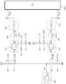
도 3은 도 2의 보상 회로의 일 실시예를 보여주는 블록도이다. 도 4는 도 3의 보상 회로의 동작을 설명하기 위한 타이밍도이다. 도 3 및 도 4가 함께 설명된다. 도 4에 도시된 시간 구간들('t0'~'t1', 't1'~'t2', 't2'~'t3', 't3'~'t4', 't4'~'t5') 각각에서의 보상 회로의 동작은 도 7 내지 도 11을 참조하여 자세하게 설명된다. 도 2를 참조하여 설명된 제 1 타겟 레벨 및 제 2 타겟 레벨은 이하 설명들에서 제 1 레벨(Lv1) 및 제 2 레벨(Lv2)인 것으로 가정된다.FIG. 3 is a block diagram showing one embodiment of the compensation circuit of FIG. 2. FIG. 4 is a timing diagram for explaining the operation of the compensation circuit of FIG. 3. FIGS. 3 and 4 are described together. The operation of the compensation circuit in each of the time sections ('t0' to 't1', 't1' to 't2', 't2' to 't3', 't3' to 't4', 't4' to 't5') illustrated in FIG. 4 is described in detail with reference to FIGS. 7 to 11. The first target level and the second target level described with reference to FIG. 2 are assumed to be the first level (Lv1) and the second level (Lv2) in the following descriptions.
지연 고정 루프(1100)는 내부 클럭 신호들(in1, in2)을 출력할 수 있다. 내부 클럭 신호들(in1, in2) 간에는 위상차가 존재할 수 있다.The delay locked loop (1100) can output internal clock signals (in1, in2). There may be a phase difference between the internal clock signals (in1, in2).
제 1 지연 회로(110)는 두 개의 인버터를 포함할 수 있다. 제 1 지연 회로(110)는 내부 클럭 신호(in1)를 지연시킬 수 있다. 다만, 설명의 편의를 위해, 제 1 지연 회로(110)에 의한 지연은 없는 것으로 가정된다.The first delay circuit (110) may include two inverters. The first delay circuit (110) may delay the internal clock signal (in1). However, for convenience of explanation, it is assumed that there is no delay by the first delay circuit (110).
제 1 스위칭 회로(120)는 상이한 트랜지스터들로 구성된 게이트 회로일 수 있다. 트랜지스터들 중 하나는 PMOS 트랜지스터이고, 나머지 하나는 NMOS 트랜지스터일 수 있다. PMOS 트랜지스터의 드레인단은 노드(n1)와 연결되고, PMOS 트랜지스터의 소스단은 노드(n2)와 연결될 수 있다. PMOS 트랜지스터는 게이트단으로 반전 내부 클럭 신호(/in1)를 인가받을 수 있다. PMOS 트랜지스터는 반전 내부 클럭 신호(/in1)에 기초하여, 노드(n1)로부터 노드(n2)로 전류를 출력할지 여부를 결정할 수 있다. NMOS 트랜지스터의 드레인단은 노드(n1)와 연결되고, NMOS 트랜지스터의 소스단은 노드(n2)와 연결될 수 있다. NMOS 트랜지스터는 게이트단으로 내부 클럭 신호(in1)를 인가받을 수 있다. NMOS 트랜지스터는 내부 클럭 신호(in1)에 기초하여, 노드(n1)로부터 노드(n2)로 전류를 출력할지 여부를 결정할 수 있다.The first switching circuit (120) may be a gate circuit composed of different transistors. One of the transistors may be a PMOS transistor, and the other may be an NMOS transistor. A drain terminal of the PMOS transistor may be connected to a node (n1), and a source terminal of the PMOS transistor may be connected to a node (n2). The PMOS transistor may receive an inverted internal clock signal (/in1) as a gate terminal. The PMOS transistor may determine whether to output current from the node (n1) to the node (n2) based on the inverted internal clock signal (/in1). A drain terminal of the NMOS transistor may be connected to the node (n1), and a source terminal of the NMOS transistor may be connected to the node (n2). The NMOS transistor may receive an internal clock signal (in1) as a gate terminal. The NMOS transistor may determine whether to output current from the node (n1) to the node (n2) based on the internal clock signal (in1).
내부 클럭 신호(in1)의 전압 레벨이 제 2 레벨(Lv2)인 경우, PMOS 트랜지스터 및 NMOS 트랜지스터는 각각 제 1 레벨(Lv1)의 반전 내부 클럭 신호(/in1) 및 제 2 레벨의 내부 클럭 신호(in1)를 수신할 수 있다. 제 1 레벨의 신호는 신호의 전압 레벨이 제 1 레벨인 것을 의미한다. 또한, 제 2 레벨의 신호는 신호의 전압 레벨이 제 2 레벨인 것을 의미한다.When the voltage level of the internal clock signal (in1) is the second level (Lv2), the PMOS transistor and the NMOS transistor can receive the inverted internal clock signal (/in1) of the first level (Lv1) and the internal clock signal (in1) of the second level, respectively. The signal of the first level means that the voltage level of the signal is the first level. In addition, the signal of the second level means that the voltage level of the signal is the second level.
제 1 레벨(Lv1)의 신호는 논리 값 '0'을 갖는 디지털 신호에 대응할 수 있다. 제 2 레벨(Lv2)의 신호는 논리 값 '1'을 갖는 디지털 신호에 대응할 수 있다. 본 명세서에서, 설명의 편의를 위해, 제 1 레벨(Lv1) 및 제 2 레벨(Lv2)은 각각 전압(VSS)의 레벨 및 전압(VDD)의 레벨과 동일한 것으로 가정된다.A signal of the first level (Lv1) may correspond to a digital signal having a logic value of '0'. A signal of the second level (Lv2) may correspond to a digital signal having a logic value of '1'. In this specification, for convenience of explanation, the first level (Lv1) and the second level (Lv2) are assumed to be equal to the level of the voltage (VSS) and the level of the voltage (VDD), respectively.
이하 설명들에서, PMOS 트랜지스터는 제 1 레벨(Lv1)의 신호가 인가되는 경우, 드레인단으로부터 소스단으로 전류를 출력하고, 제 2 레벨(Lv2)의 신호가 인가되는 경우, 전류를 출력하지 않는 것으로 가정된다. 또한, NMOS 트랜지스터는 제 2 레벨(Lv2)의 신호가 인가되는 경우, 드레인단으로부터 소스단으로 전류를 출력하고, 제 1 레벨(Lv1)의 신호가 인가되는 경우, 전류를 출력하지 않는 것으로 가정된다.In the following descriptions, it is assumed that a PMOS transistor outputs current from the drain terminal to the source terminal when a signal of the first level (Lv1) is applied, and does not output current when a signal of the second level (Lv2) is applied. In addition, it is assumed that an NMOS transistor outputs current from the drain terminal to the source terminal when a signal of the second level (Lv2) is applied, and does not output current when a signal of the first level (Lv1) is applied.
시간 구간('t0'~'t1')에서처럼 제 2 레벨(Lv2)의 내부 클럭 신호(in1) 및 제 1 레벨(Lv1)의 반전 내부 클럭 신호(/in1)가 수신되는 경우, 제 1 스위칭 회로(120)는 노드(n1)로부터 노드(n2)로 전류를 출력할 수 있다. 시간 구간('t1'~'t2')에서처럼 제 1 레벨의 내부 클럭 신호(in1) 및 제 2 레벨의 반전 내부 클럭 신호(/in1)가 수신되는 경우, 제 1 스위칭 회로(120)는 노드(n1)로부터 노드(n2)로 전류를 출력하지 않을 수 있다.When the internal clock signal (in1) of the second level (Lv2) and the inverted internal clock signal (/in1) of the first level (Lv1) are received, such as in the time section ('t0' to 't1'), the first switching circuit (120) can output current from the node (n1) to the node (n2). When the internal clock signal (in1) of the first level and the inverted internal clock signal (/in1) of the second level are received, such as in the time section ('t1' to 't2'), the first switching circuit (120) can not output current from the node (n1) to the node (n2).
이하 설명들에서, 노드(n1)가 노드(n2)로 연결되 것은 노드(n1)로부터 노드(n2)로 전류가 출력되는 것을 의미한다. 또한, 노드(n1)가 노드(n2)로부터 연결해제되는 것은 노드(n1)로부터 노드(n2)로 전류가 출력되지 않는 것을 의미한다.In the following descriptions, node (n1) being connected to node (n2) means that current is output from node (n1) to node (n2). Also, node (n1) being disconnected from node (n2) means that current is not output from node (n1) to node (n2).
노드(n2)의 전압 레벨은 노드(n1)가 노드(n2)와 연결되는 경우, 노드(n1)의 전압 레벨과 동일할 수 있다. 노드(n2)가 노드(n1)로부터 연결해제되는 경우, 노드(n2)의 전압 레벨은 도 2의 제 1 펄스 조절 회로(130)의 동작에 의해 결정될 수 있다.The voltage level of node (n2) may be the same as the voltage level of node (n1) when node (n1) is connected to node (n2). When node (n2) is disconnected from node (n1), the voltage level of node (n2) may be determined by the operation of the first pulse control circuit (130) of Fig. 2.
제 1 펄스 조절 회로(130)는 트랜지스터들(131, 133, 134, 135) 및 래치 회로(132)를 포함할 수 있다.The first pulse control circuit (130) may include transistors (131, 133, 134, 135) and a latch circuit (132).
래치 회로(132)는 노드(n2)로 입력된 신호의 위상을 반전시킬 수 있다. 래치 회로(132)는 위상이 반전된 신호를 노드(n3)로 출력할 수 있다. 예로서, 래치 회로(132)는 인버터 루프일 수 있다. 구체적으로, 래치 회로(132)는 노드(n2)의 전압 레벨이 제 1 레벨(Lv1)인 경우, 노드(n3)의 전압 레벨이 제 2 레벨(Lv2)이 되도록 동작할 수 있다. 또한, 래치 회로(132)는 노드(n2)의 전압 레벨이 제 2 레벨(Lv2)인 경우, 노드(n3)의 전압 레벨이 제 1 레벨(Lv1)이 되도록 동작할 수 있다.The latch circuit (132) can invert the phase of a signal input to the node (n2). The latch circuit (132) can output a signal with an inverted phase to the node (n3). For example, the latch circuit (132) can be an inverter loop. Specifically, the latch circuit (132) can operate so that the voltage level of the node (n3) becomes the second level (Lv2) when the voltage level of the node (n2) becomes the first level (Lv1). In addition, the latch circuit (132) can operate so that the voltage level of the node (n3) becomes the first level (Lv1) when the voltage level of the node (n2) becomes the second level (Lv2).
트랜지스터(131)는 PMOS 트랜지스터일 수 있다. 트랜지스터(131)의 드레인단은 전원(VDD) 공급단과 연결되고, 소스단은 트랜지스터(133)의 드레인단과 연결될 수 있다. 또한, 트랜지스터(131)는 게이트 단으로 내부 클럭 신호(in1)를 인가받을 수 있다. 트랜지스터(131)는 내부 클럭 신호(in1)에 기초하여, 전원(VDD) 공급단으로부터 트랜지스터(133)로 제 1 조절 전류를 출력할지 여부를 결정할 수 있다. 다만, 본 발명은 이에 한정되지 않고, 트랜지스터(131)는 NMOS 트랜지스터일 수 있다. 이 경우, 트랜지스터(131)는 게이트 단으로 반전 내부 클럭 신호(/in1)를 인가받을 수 있다. 본 명세서에서 설명되는 NMOS 트랜지스터는 모두 PMOS 트랜지스터로 대체될 수 있으며, PMOS 트랜지스터는 모두 MMOS 트랜지스터로 대체될 수 있다. 다만 이 경우, 대체 트랜지스터의 게이트단으로 입력되는 신호는 본래 트랜지스터의 게이트단으로 입력되는 신호의 위상이 반전된 신호일 수 있다. 또한, 본 발명의 트랜지스터는 게이트단으로 입력되는 신호를 제어 신호로서 인가받아 동작하는 스위치(switch)로 교체될 수 있다.The transistor (131) may be a PMOS transistor. The drain terminal of the transistor (131) may be connected to the power supply terminal (VDD), and the source terminal may be connected to the drain terminal of the transistor (133). In addition, the transistor (131) may receive an internal clock signal (in1) through its gate terminal. The transistor (131) may determine whether to output a first regulated current from the power supply terminal (VDD) to the transistor (133) based on the internal clock signal (in1). However, the present invention is not limited thereto, and the transistor (131) may be an NMOS transistor. In this case, the transistor (131) may receive an inverted internal clock signal (/in1) through its gate terminal. All of the NMOS transistors described herein may be replaced with PMOS transistors, and all of the PMOS transistors may be replaced with MMOS transistors. However, in this case, the signal input to the gate terminal of the replacement transistor may be a signal whose phase is inverted from the signal input to the gate terminal of the original transistor. In addition, the transistor of the present invention may be replaced with a switch that operates by receiving a signal input to the gate terminal as a control signal.
트랜지스터(131)는 제 1 레벨(Lv1)의 내부 클럭 신호(in1)가 수신되는 경우, 전원(VDD) 공급단으로부터 트랜지스터(133)로 제 1 조절 전류를 출력할 수 있다. 트랜지스터(131)는 제 2 레벨(Lv2)의 내부 클럭 신호(in1)가 수신되는 경우, 전원(VDD) 공급단으로부터 트랜지스터(133)로 제 1 조절 전류를 출력하지 않을 수 있다.The transistor (131) can output a first regulated current from the power supply (VDD) to the transistor (133) when an internal clock signal (in1) of a first level (Lv1) is received. The transistor (131) can not output the first regulated current from the power supply (VDD) to the transistor (133) when an internal clock signal (in1) of a second level (Lv2) is received.
트랜지스터(133)는 PMOS 트랜지스터일 수 있다. 트랜지스터(133)의 드레인단은 트랜지스터(131)의 소스단과 연결되고, 소스단은 노드(p0)와 연결될 수 있다. 또한, 트랜지스터(133)는 게이트 단으로 신호(a0)를 인가받을 수 있다. 신호(a0)는 노드(n3)로부터 트랜지스터(133)로 출력되는 전압 신호일 수 있다. 신호(a0)의 전압 레벨은 노드(n3)의 전압 레벨과 동일할 수 있다. 트랜지스터(133)는 신호(a0)에 기초하여, 트랜지스터(131)로부터 전달받은 제 1 조절 전류를 노드(p0)로 출력할지 여부를 결정할 수 있다.The transistor (133) may be a PMOS transistor. The drain terminal of the transistor (133) may be connected to the source terminal of the transistor (131), and the source terminal may be connected to the node (p0). In addition, the transistor (133) may receive a signal (a0) through a gate terminal. The signal (a0) may be a voltage signal output from the node (n3) to the transistor (133). The voltage level of the signal (a0) may be the same as the voltage level of the node (n3). The transistor (133) may determine whether to output the first regulating current received from the transistor (131) to the node (p0) based on the signal (a0).
제 1 레벨(Lv1)의 신호(a0)가 수신되는 경우, 트랜지스터(133)는 노드(p0)로 제 1 조절 전류를 출력할 수 있다. 제 2 레벨(Lv2)의 신호(a0)가 수신되는 경우, 트랜지스터(133)는 노드(p0)로 제 1 조절 전류를 출력하지 않을 수 있다.When a signal (a0) of the first level (Lv1) is received, the transistor (133) can output the first regulated current to the node (p0). When a signal (a0) of the second level (Lv2) is received, the transistor (133) may not output the first regulated current to the node (p0).
즉, 시간 구간('t1'~'t2)에서처럼 트랜지스터들(131, 133)로 각각 제 1 레벨(Lv1)의 내부 클럭 신호(in1) 및 제 1 레벨의 신호(a0)가 인가되는 경우, 트랜지스터들(131, 133)은 전원(VDD) 공급단으로부터 노드(p0)로 제 1 조절 전류를 출력할 수 있다. 노드(p0)로 제 1 조절 전류가 출력되는 경우, 노드(p0)의 전압 레벨은 증가할 수 있다.That is, when the internal clock signal (in1) of the first level (Lv1) and the signal (a0) of the first level are applied to the transistors (131, 133) respectively during the time period ('t1' to 't2), the transistors (131, 133) can output the first regulated current from the power supply (VDD) to the node (p0). When the first regulated current is output to the node (p0), the voltage level of the node (p0) can increase.
트랜지스터(134)는 NMOS 트랜지스터일 수 있다. 트랜지스터(134)의 드레인 단은 노드(n2)와 연결되고, 소스단은 트랜지스터(135)의 드레인단과 연결된다. 트랜지스터(134)는 게이트 단으로 신호(as0)를 인가받을 수 있다. 신호(as0)는 노드(p0)로부터 트랜지스터(134)의 게이트 단으로 출력될 수 있다. 신호(as0)의 전압 레벨은 노드(p0)의 전압 레벨과 동일할 수 있다. 트랜지스터(134)는 신호(as0)에 기초하여, 노드(n2)로부터 트랜지스터(135)로 제 3 조절 전류를 출력할지 여부를 결정할 수 있다.The transistor (134) may be an NMOS transistor. The drain terminal of the transistor (134) is connected to the node (n2), and the source terminal is connected to the drain terminal of the transistor (135). The transistor (134) may receive a signal (as0) through its gate terminal. The signal (as0) may be output from the node (p0) to the gate terminal of the transistor (134). The voltage level of the signal (as0) may be the same as the voltage level of the node (p0). The transistor (134) may determine whether to output a third regulating current from the node (n2) to the transistor (135) based on the signal (as0).
제 1 레벨(Lv1)의 신호(as0)가 수신되는 경우, 트랜지스터(134)는 노드(n2)로부터 트랜지스터(135)로 제 3 조절 전류를 출력하지 않을 수 있다. 제 2 레벨(Lv2)의 신호(as0)가 수신되는 경우, 트랜지스터(134)는 노드(n2)로부터 트랜지스터(135)로 제 3 조절 전류를 출력할 수 있다.When a signal (as0) of the first level (Lv1) is received, the transistor (134) may not output the third regulated current from the node (n2) to the transistor (135). When a signal (as0) of the second level (Lv2) is received, the transistor (134) may output the third regulated current from the node (n2) to the transistor (135).
트랜지스터(135)는 NMOS 트랜지스터일 수 있다. 트랜지스터(135)의 드레인 단은 트랜지스터(134)의 소스단과 연결되고, 소스단은 전압(VSS) 접지단과 연결된다. 트랜지스터(135)는 게이트 단으로 반전 내부 클럭 신호(/in1)를 인가받을 수 있다. 트랜지스터(134)는 반전 내부 클럭 신호(/in1)에 기초하여, 트랜지스터(134)로부터 전달받은 제 3 조절 전류를 전압(VSS) 접지단으로 출력할지 여부를 결정할 수 있다.The transistor (135) may be an NMOS transistor. The drain terminal of the transistor (135) is connected to the source terminal of the transistor (134), and the source terminal is connected to the voltage (VSS) ground terminal. The transistor (135) may receive an inverted internal clock signal (/in1) to a gate terminal. The transistor (134) may determine whether to output the third regulated current received from the transistor (134) to the voltage (VSS) ground terminal based on the inverted internal clock signal (/in1).
제 1 레벨(Lv1)의 반전 내부 클럭 신호(/in1)가 인가되는 경우, 트랜지스터(135)는 전압(VSS) 접지단으로 제 3 조절 전류를 출력하지 않을 수 있다. 제 2 레벨(Lv2)의 반전 내부 클럭 신호(/in1)가 인가되는 경우, 트랜지스터(135)는 전압(VSS) 접지단으로 제 3 조절 전류를 출력할 수 있다.When the inverted internal clock signal (/in1) of the first level (Lv1) is applied, the transistor (135) may not output the third regulated current to the voltage (VSS) ground terminal. When the inverted internal clock signal (/in1) of the second level (Lv2) is applied, the transistor (135) may output the third regulated current to the voltage (VSS) ground terminal.
시간 구간('t2'~'t3')에서처럼 트랜지스터들(134, 135)로 각각 제 2 레벨(Lv2)의 신호(as0) 및 제 2 레벨(Lv2)의 반전 내부 클럭 신호(/in1)가 수신되는 경우, 트랜지스터들(134, 135)은 노드(n2)로부터 전압(VSS) 접지단으로 제 3 조절 전류를 출력할 수 있다. 노드(n2)로부터 전압(VSS) 접지단으로 제 3 조절 전류가 출력되면, 노드(n2)의 전압 레벨이 제 2 레벨(Lv2)보다 낮아지고, 노드(n3)의 전압 레벨이 제 1 레벨(Lv1)보다 높아질 수 있다. 따라서, 트랜지스터(133)는 노드(p0)로 제 1 조절 전류를 출력하지 않을 수 있다.When the signal (as0) of the second level (Lv2) and the inverted internal clock signal (/in1) of the second level (Lv2) are received by the transistors (134, 135) in the time section ('t2' to 't3'), the transistors (134, 135) can output the third regulated current from the node (n2) to the voltage (VSS) ground terminal. When the third regulated current is output from the node (n2) to the voltage (VSS) ground terminal, the voltage level of the node (n2) can become lower than the second level (Lv2), and the voltage level of the node (n3) can become higher than the first level (Lv1). Therefore, the transistor (133) may not output the first regulated current to the node (p0).
즉, 트랜지스터들(131, 133)은 노드(p0)의 전압 레벨이 제 2 레벨로 증가할 때까지 제 1 조절 전류를 출력하고, 노드(p0)의 전압 레벨이 제 2 레벨에 도달하면 제 1 조절 전류를 출력하는 것을 중단할 수 있다.That is, the transistors (131, 133) can output the first regulated current until the voltage level of the node (p0) increases to the second level, and can stop outputting the first regulated current when the voltage level of the node (p0) reaches the second level.
제 2 지연 회로(150)는 두 개의 인버터를 포함할 수 있다. 제 2 지연 회로(150)는 내부 클럭 신호(in2)를 지연시킬 수 있다. 다만, 설명의 편의를 위해, 제 2 지연 회로(150)에 의한 지연은 없는 것으로 가정된다.The second delay circuit (150) may include two inverters. The second delay circuit (150) may delay the internal clock signal (in2). However, for convenience of explanation, it is assumed that there is no delay by the second delay circuit (150).
제 2 스위칭 회로(160)는 상이한 트랜지스터들로 구성된 게이트 회로일 수 있다. 트랜지스터들 중 하나는 PMOS 트랜지스터이고, 나머지 하나는 NMOS 트랜지스터일 수 있다. 제 2 스위칭 회로(160)는 제 1 스위칭 회로(120)와 실질적으로 동일한 동작을 제공할 수 있다. 따라서, 이하 중복되는 설명은 생략된다.The second switching circuit (160) may be a gate circuit composed of different transistors. One of the transistors may be a PMOS transistor, and the other may be an NMOS transistor. The second switching circuit (160) may provide substantially the same operation as the first switching circuit (120). Therefore, any duplicate description is omitted below.
시간 구간('t0'~'t3')에서처럼 제 1 레벨의 내부 클럭 신호(in2) 및 제 2 레벨의 반전 내부 클럭 신호(/in2)가 수신되는 경우, 제 2 스위칭 회로(160)는 노드(n5)로부터 노드(n6)로 전류를 출력할 수 있다. 시간 구간('t3'~'t4')에서처럼 제 2 레벨의 내부 클럭 신호(in2) 및 제 1 레벨의 반전 내부 클럭 신호(/in2)가 수신되는 경우, 제 2 스위칭 회로(160)는 노드(n5)로부터 노드(n6)로 전류를 출력하지 않을 수 있다.When the first-level internal clock signal (in2) and the second-level inverted internal clock signal (/in2) are received, such as in the time section ('t0' to 't3'), the second switching circuit (160) can output current from the node (n5) to the node (n6). When the second-level internal clock signal (in2) and the first-level inverted internal clock signal (/in2) are received, such as in the time section ('t3' to 't4'), the second switching circuit (160) can not output current from the node (n5) to the node (n6).
노드(n5)가 노드(n6)와 연결되는 경우, 노드(n6)의 전압 레벨은 노드(n5)의 전압 레벨과 동일할 수 있다. 그러나, 노드(n6)가 노드(n5)로부터 연결해제되는 경우, 노드(n6)의 전압 레벨은 노드(n5)의 전압 레벨과 동일하지 않을 수 있다. 이 경우, 노드(n6)의 전압 레벨은 도 2의 제 2 펄스 조절 회로(170)의 동작에 의해 결정될 수 있다.When node (n5) is connected to node (n6), the voltage level of node (n6) may be the same as the voltage level of node (n5). However, when node (n6) is disconnected from node (n5), the voltage level of node (n6) may not be the same as the voltage level of node (n5). In this case, the voltage level of node (n6) may be determined by the operation of the second pulse regulation circuit (170) of FIG. 2.
제 2 펄스 조절 회로(170)는 트랜지스터들(171, 173, 174, 175) 및 래치 회로(172)를 포함할 수 있다.The second pulse control circuit (170) may include transistors (171, 173, 174, 175) and a latch circuit (172).
래치 회로(172)는 노드(n6)로 입력된 신호의 위상을 반전시킬 수 있다. 래치 회로(172)는 래치 회로(132)와 실질적으로 동일한 동작을 제공할 수 있다.The latch circuit (172) can invert the phase of the signal input to the node (n6). The latch circuit (172) can provide substantially the same operation as the latch circuit (132).
트랜지스터(171)는 NMOS 트랜지스터일 수 있다. 트랜지스터(171)의 드레인단은 노드(p0)와 연결되고, 소스단은 전원(VSS) 접지단과 연결될 수 있다. 또한, 트랜지스터(171)는 게이트 단으로 신호(b0)를 인가받을 수 있다. 신호(b0)는 노드(n7)로부터 트랜지스터(171)의 게이트단으로 출력되는 신호일 수 있다. 신호(b0)의 전압 레벨은 노드(n7)의 전압 레벨과 동일할 수 있다. 트랜지스터(171)는 신호(b0)에 기초하여, 노드(p0)로부터 트랜지스터(173)로 제 2 조절 전류를 출력할지 여부를 결정할 수 있다.The transistor (171) may be an NMOS transistor. The drain terminal of the transistor (171) may be connected to the node (p0), and the source terminal may be connected to the power supply (VSS) ground terminal. In addition, the transistor (171) may receive a signal (b0) through its gate terminal. The signal (b0) may be a signal output from the node (n7) to the gate terminal of the transistor (171). The voltage level of the signal (b0) may be the same as the voltage level of the node (n7). The transistor (171) may determine whether to output the second regulating current from the node (p0) to the transistor (173) based on the signal (b0).
트랜지스터(171)는 제 1 레벨(Lv1)의 신호(b0)가 수신되는 경우, 노드(p0)로부터 트랜지스터(173)로 제 2 조절 전류를 출력하지 않을 수 있다. 트랜지스터(171)는 제 2 레벨(Lv2)의 신호(b0)가 수신되는 경우, 노드(p0)로부터 트랜지스터(173)로 제 2 조절 전류를 출력할 수 있다.When a signal (b0) of the first level (Lv1) is received, the transistor (171) may not output the second regulated current from the node (p0) to the transistor (173). When a signal (b0) of the second level (Lv2) is received, the transistor (171) may output the second regulated current from the node (p0) to the transistor (173).
트랜지스터(173)는 NMOS 트랜지스터일 수 있다. 트랜지스터(173)의 드레인단은 트랜지스터(171)의 소스단과 연결되고, 소스단은 전원(VSS)의 접지단과 연결될 수 있다. 또한, 트랜지스터(173)는 게이트 단으로 내부 클럭 신호(in2)를 인가받을 수 있다. 트랜지스터(173)는 내부 클럭 신호(in2)에 기초하여, 트랜지스터(171)로부터 전달받은 제 2 조절 전류를 전원(VSS) 접지단으로 출력할지 여부를 결정할 수 있다.The transistor (173) may be an NMOS transistor. The drain terminal of the transistor (173) may be connected to the source terminal of the transistor (171), and the source terminal may be connected to the ground terminal of the power supply (VSS). In addition, the transistor (173) may receive an internal clock signal (in2) to a gate terminal. The transistor (173) may determine whether to output the second control current received from the transistor (171) to the ground terminal of the power supply (VSS) based on the internal clock signal (in2).
제 1 레벨(Lv1)의 내부 클럭 신호(in2)가 수신되는 경우, 트랜지스터(173)는 전원(VSS) 접지단으로 제 1 조절 전류를 출력하지 않을 수 있다. 제 2 레벨(Lv2)의 내부 클럭 신호(in2)가 수신되는 경우, 트랜지스터(173)는 전원(VSS) 접지단으로 제 2 조절 전류를 출력할 수 있다.When an internal clock signal (in2) of the first level (Lv1) is received, the transistor (173) may not output the first regulated current to the power supply (VSS) ground terminal. When an internal clock signal (in2) of the second level (Lv2) is received, the transistor (173) may output the second regulated current to the power supply (VSS) ground terminal.
즉, 시간 구간('t3'~'t4')에서처럼, 트랜지스터들(171, 173)로 각각 제 2 레벨(Lv2)의 신호(b0) 및 제 2 레벨(Lv2)의 내부 클럭 신호(in2)가 인가되는 경우, 트랜지스터들(171, 173)은 노드(p0)로부터 전원(VSS) 접지단으로 제 2 조절 전류를 출력할 수 있다. 노드(p0)로부터 전원(VSS) 접지단으로 제 2 조절 전류가 출력되는 경우, 노드(p0)의 전압 레벨은 감소할 수 있다.That is, in the time section ('t3' to 't4'), when a signal (b0) of the second level (Lv2) and an internal clock signal (in2) of the second level (Lv2) are applied to the transistors (171, 173), respectively, the transistors (171, 173) can output a second regulated current from the node (p0) to the power supply (VSS) ground terminal. When the second regulated current is output from the node (p0) to the power supply (VSS) ground terminal, the voltage level of the node (p0) can decrease.
트랜지스터(174)는 PMOS 트랜지스터일 수 있다. 트랜지스터(174)의 드레인 단은 전원(VDD) 공급단과 연결되고, 소스단은 트랜지스터(175)의 드레인단과 연결될 수 있다. 트랜지스터(174)는 게이트 단으로 반전 내부 클럭 신호(/in2)를 인가받을 수 있다. 트랜지스터(174)는 반전 내부 클럭 신호(/in2)에 기초하여, 전원(VDD) 공급단으로부터 트랜지스터(175)로 제 4 조절 전류를 출력할지 여부를 결정할 수 있다.The transistor (174) may be a PMOS transistor. The drain terminal of the transistor (174) may be connected to the power supply terminal (VDD), and the source terminal may be connected to the drain terminal of the transistor (175). The transistor (174) may receive an inverted internal clock signal (/in2) as a gate terminal. The transistor (174) may determine whether to output a fourth regulated current from the power supply terminal (VDD) to the transistor (175) based on the inverted internal clock signal (/in2).
제 1 레벨(Lv1)의 반전 내부 클럭 신호(/in2)가 수신되는 경우, 트랜지스터(174)는 전원(VDD) 공급단으로부터 트랜지스터(175)로 제 4 조절 전류를 출력할 수 있다. 제 2 레벨(Lv2)의 반전 내부 클럭 신호(/in2)가 수신되는 경우, 트랜지스터(174)는 전원(VDD) 공급단으로부터 트랜지스터(175)로 제 4 조절 전류를 출력하지 않을 수 있다.When the inverted internal clock signal (/in2) of the first level (Lv1) is received, the transistor (174) can output the fourth regulated current from the power supply (VDD) to the transistor (175). When the inverted internal clock signal (/in2) of the second level (Lv2) is received, the transistor (174) may not output the fourth regulated current from the power supply (VDD) to the transistor (175).
트랜지스터(175)는 PMOS 트랜지스터일 수 있다. 트랜지스터(175)의 드레인 단은 트랜지스터(174)의 소스단과 연결되고, 소스단은 노드(n6)와 연결될 수 있다. 트랜지스터(175)는 게이트 단으로 신호(as0)를 인가받을 수 있다. 신호(as0)는 노드(p0)로부터 트랜지스터(175)의 게이트 단으로 출력될 수 있다. 트랜지스터(174)는 신호(as0)에 기초하여, 트랜지스터(174)로부터 전달받은 제 4 조절 전류를 노드(n6)로 출력할지 여부를 결정할 수 있다.Transistor (175) may be a PMOS transistor. A drain terminal of transistor (175) may be connected to a source terminal of transistor (174), and the source terminal may be connected to node (n6). Transistor (175) may receive a signal (as0) through a gate terminal. The signal (as0) may be output from node (p0) to the gate terminal of transistor (175). Transistor (174) may determine whether to output the fourth regulating current received from transistor (174) to node (n6) based on the signal (as0).
제 1 레벨(Lv1)의 신호(as0)가 인가되는 경우, 트랜지스터(175)는 노드(n6)로 제 4 조절 전류를 출력할 수 있다. 제 2 레벨(Lv2)의 신호(as0)가 인가되는 경우, 트랜지스터(175)는 노드(n6)로 제 4 조절 전류를 출력하지 않을 수 있다.When a signal (as0) of the first level (Lv1) is applied, the transistor (175) can output the fourth regulated current to the node (n6). When a signal (as0) of the second level (Lv2) is applied, the transistor (175) may not output the fourth regulated current to the node (n6).
시간 구간('t3'~'t4')에서처럼 트랜지스터들(174, 175)로 각각 제 1 레벨(Lv1)의 반전 내부 클럭 신호(/in2) 및 제 1 레벨(Lv1)의 신호(as0)가 수신되는 경우, 트랜지스터들(174, 175)은 전원(VDD) 공급단으로부터 노드(n6)로 제 4 조절 전류를 출력할 수 있다. 전원(VDD) 공급단으로부터 노드(n6)로 제 4 조절 전류가 출력되면, 노드(n6)의 전압 레벨이 제 1 레벨(Lv1)보다 높아지고, 노드(n7)의 전압 레벨이 제 2 레벨(Lv2)보다 낮아질 수 있다.When the inverted internal clock signal (/in2) of the first level (Lv1) and the signal (as0) of the first level (Lv1) are received by the transistors (174, 175) in the time section ('t3' to 't4'), the transistors (174, 175) can output the fourth regulated current from the power supply (VDD) to the node (n6). When the fourth regulated current is output from the power supply (VDD) to the node (n6), the voltage level of the node (n6) can become higher than the first level (Lv1), and the voltage level of the node (n7) can become lower than the second level (Lv2).
즉, 트랜지스터들(171, 173)은 노드(p0)의 전압 레벨이 제 1 레벨로 감소할 때까지 제 2 조절 전류를 출력하고, 노드(p0)의 전압 레벨이 제 1 레벨에 도달하면 제 2 조절 전류를 출력하는 것을 중단할 수 있다.That is, the transistors (171, 173) can output the second regulated current until the voltage level of the node (p0) decreases to the first level, and can stop outputting the second regulated current when the voltage level of the node (p0) reaches the first level.
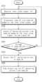
도 5는 도 3의 보상 회로의 동작을 설명하기 위한 흐름도이다.Figure 5 is a flowchart for explaining the operation of the compensation circuit of Figure 3.
도 5를 참조하여, 도 4의 시간 구간('t1'~'t2')에서의 도 3의 보상 회로(100)의 동작이 설명된다.Referring to FIG. 5, the operation of the compensation circuit (100) of FIG. 3 in the time section ('t1' to 't2') of FIG. 4 is explained.
S110 동작에서, 보상 회로(100)는 제 1 레벨(Lv1)의 내부 클럭 신호(in1)를 수신할 수 있다.In the S110 operation, the compensation circuit (100) can receive an internal clock signal (in1) of the first level (Lv1).
S120 동작에서, 제 1 스위칭 회로(120)는 제 1 레벨(Lv1)의 내부 클럭 신호(in1)가 수신되는 경우, 노드(n1)를 노드(n2)로부터 연결해제할 수 있다. 이 경우, 노드(n2)의 전압 레벨은 시각('t1') 이전에서의 전압 레벨로 유지될 수 있다. 래치 회로(132)에 의해, 노드(n3)의 전압 레벨은 제 1 레벨(Lv1)로 유지될 수 있다.In the S120 operation, the first switching circuit (120) can disconnect the node (n1) from the node (n2) when an internal clock signal (in1) of the first level (Lv1) is received. In this case, the voltage level of the node (n2) can be maintained at the voltage level before the time ('t1'). By the latch circuit (132), the voltage level of the node (n3) can be maintained at the first level (Lv1).
S130 동작에서, 트랜지스터들(131, 133)은 각각 제 1 레벨(Lv1)의 내부 클럭 신호(in1) 및 제 1 레벨(Lv1)의 신호(a0)를 인가받을 수 있다. 트랜지스터들(131, 133)은 내부 클럭 신호(in1) 및 신호(a0)에 기초하여, 전원(VDD) 공급단으로부터 노드(p0)로 제 1 조절 전류를 출력할 수 있다.In the S130 operation, the transistors (131, 133) can receive an internal clock signal (in1) of a first level (Lv1) and a signal (a0) of a first level (Lv1), respectively. The transistors (131, 133) can output a first regulated current from a power supply (VDD) to a node (p0) based on the internal clock signal (in1) and the signal (a0).
S140 동작에서, 트랜지스터(134)는 노드(p0)의 전압 레벨이 제 2 레벨(Lv2)인지 여부에 따라, 노드(n2)로부터 트랜지스터(135)로 제 3 조절 전류를 출력할지 여부를 결정할 수 있다.In operation S140, the transistor (134) can determine whether to output a third regulated current from the node (n2) to the transistor (135) depending on whether the voltage level of the node (p0) is the second level (Lv2).
노드(p0)의 전압 레벨이 제 2 레벨(Lv2)에 도달하지 않은 경우, S130 동작이 다시 수행될 수 있다.If the voltage level of node (p0) does not reach the second level (Lv2), operation S130 can be performed again.
노드(p0)의 전압 레벨이 제 2 레벨(Lv2)에 도달한 경우, S150 동작이 수행될 수 있다. S150 동작에서, 트랜지스터(134)는 노드(n2)로부터 트랜지스터(135)로 제 3 조절 전류를 출력할 수 있다. 트랜지스터(135) 역시, 전달받은 제 3 조절 전류를 전원(VSS) 접지단으로 출력할 수 있다. 따라서, 노드(n2)의 전압 레벨이 감소할 수 있다.When the voltage level of the node (p0) reaches the second level (Lv2), the S150 operation can be performed. In the S150 operation, the transistor (134) can output a third regulated current from the node (n2) to the transistor (135). The transistor (135) can also output the received third regulated current to the power supply (VSS) ground terminal. Accordingly, the voltage level of the node (n2) can decrease.
S160 동작에서, 노드(n2)의 전압 레벨이 제 2 레벨(Lv2)보다 낮아지면, 트랜지스터(133)는 노드(p0)로 제 1 조절 전류를 출력하는 것을 중단할 수 있다.In the S160 operation, when the voltage level of the node (n2) becomes lower than the second level (Lv2), the transistor (133) can stop outputting the first regulated current to the node (p0).
도 6은 도 3의 보상 회로의 동작을 설명하기 위한 흐름도이다.Figure 6 is a flowchart for explaining the operation of the compensation circuit of Figure 3.
도 6을 참조하여, 도 4의 시간 구간('t3'~'t4')에서의 도 3의 보상 회로(100)의 동작이 설명된다.Referring to FIG. 6, the operation of the compensation circuit (100) of FIG. 3 in the time section ('t3' to 't4') of FIG. 4 is explained.
S210 동작에서, 보상 회로(100)는 제 2 레벨(Lv2)의 내부 클럭 신호(in2)를 수신할 수 있다.In operation S210, the compensation circuit (100) can receive an internal clock signal (in2) of the second level (Lv2).
S220 동작에서, 제 2 스위칭 회로(160)는 제 2 레벨(Lv2)의 내부 클럭 신호(in2)가 수신되는 경우, 노드(n5)를 노드(n6)로부터 연결해제할 수 있다. 이 경우, 노드(n6)의 전압 레벨은 시각('t3') 이전에서의 전압 레벨로 유지될 수 있다. 래치 회로(172)에 의해, 노드(n7)의 전압 레벨은 제 2 레벨(Lv2)로 유지될 수 있다.In the S220 operation, the second switching circuit (160) can disconnect the node (n5) from the node (n6) when the internal clock signal (in2) of the second level (Lv2) is received. In this case, the voltage level of the node (n6) can be maintained at the voltage level before the time ('t3'). By the latch circuit (172), the voltage level of the node (n7) can be maintained at the second level (Lv2).
S230 동작에서, 트랜지스터들(171, 173)은 각각 제 2 레벨(Lv2)의 내부 클럭 신호(in2) 및 제 2 레벨(Lv2)의 신호(b0)를 인가받을 수 있다. 트랜지스터들(171, 173)은 내부 클럭 신호(in2) 및 신호(b0)에 기초하여, 노드(p0)로부터 전원(VSS) 접지단으로부터 제 3 조절 전류를 출력할 수 있다.In the S230 operation, the transistors (171, 173) can receive an internal clock signal (in2) of a second level (Lv2) and a signal (b0) of a second level (Lv2), respectively. The transistors (171, 173) can output a third regulated current from the power supply (VSS) ground terminal from the node (p0) based on the internal clock signal (in2) and the signal (b0).
S240 동작에서, 트랜지스터(175)는 노드(p0)의 전압 레벨이 제 1 레벨(Lv1)인지 여부에 따라, 트랜지스터(174)로부터 노드(n6)로 제 4 조절 전류를 출력할지 여부를 결정할 수 있다.In the S240 operation, the transistor (175) can determine whether to output the fourth regulated current from the transistor (174) to the node (n6) depending on whether the voltage level of the node (p0) is the first level (Lv1).
노드(p0)의 전압 레벨이 제 1 레벨(Lv1)에 도달하지 않은 경우, S230 동작이 다시 수행될 수 있다. 또한, 트랜지스터(175)는 트랜지스터(174)로부터 노드(n6)로 제 4 조절 전류를 출력하지 않을 수 있다.If the voltage level of node (p0) does not reach the first level (Lv1), operation S230 may be performed again. In addition, transistor (175) may not output the fourth regulated current from transistor (174) to node (n6).
노드(p0)의 전압 레벨이 제 1 레벨(Lv1)에 도달한 경우, S250 동작이 수행될 수 있다. S250 동작에서, 트랜지스터(174)는 전원(VVD) 공급단으로부터 트랜지스터(175)로 제 4 조절 전류를 출력할 수 있다. 트랜지스터(175)는 전달받은 제 4 조절 전류를 노드(n6)로 출력할 수 있다. 따라서, 노드(n6)의 전압 레벨이 높아질 수 있다.When the voltage level of the node (p0) reaches the first level (Lv1), the S250 operation can be performed. In the S250 operation, the transistor (174) can output a fourth regulated current from the power supply (VVD) to the transistor (175). The transistor (175) can output the received fourth regulated current to the node (n6). Therefore, the voltage level of the node (n6) can be increased.
S260 동작에서, 노드(n6)의 전압 레벨이 제 1 레벨(Lv1)보다 높아지면, 트랜지스터(171)는 노드(p0)로부터 제 2 조절 전류를 출력하는 것을 중단할 수 있다.In operation S260, when the voltage level of node (n6) becomes higher than the first level (Lv1), the transistor (171) can stop outputting the second regulated current from node (p0).
도 7은 특정 시간 구간에서 도 3의 보상 회로의 동작을 설명하기 위한 블록도이다. 도 7을 참조하여서는, 도 4의 시간 구간('t0'~'t1')에서의 도 3의 보상 회로(100)의 동작이 설명된다. 이하 도면들에서, “in1=1” 표시는 내부 클럭 신호(in1)의 전압 레벨이 제 2 레벨(Lv2)임을 의미한다. 또한, “in1=0” 표시는 내부 클럭 신호(in1)의 전압 레벨이 제 1 레벨(Lv1)임을 의미한다. 상기 표기법은 나머지 신호들에도 적용된다.FIG. 7 is a block diagram for explaining the operation of the compensation circuit of FIG. 3 in a specific time section. Referring to FIG. 7, the operation of the compensation circuit (100) of FIG. 3 in the time section ('t0' to 't1') of FIG. 4 is explained. In the drawings below, the notation “in1=1” means that the voltage level of the internal clock signal (in1) is the second level (Lv2). In addition, the notation “in1=0” means that the voltage level of the internal clock signal (in1) is the first level (Lv1). The above notation is also applied to the remaining signals.
제 2 레벨(Lv2)의 내부 클럭 신호(in1)가 인가되므로, 제 1 스위칭 회로(120)는 노드(n1)와 노드(n2)를 연결할 수 있다. 따라서, 노드(n2)의 전압 레벨은 내부 클럭 신호(in1)의 전압 레벨과 동일할 수 있다. 노드(n2)의 전압 레벨이 제 2 레벨(Lv2)이므로, 노드(n3)의 전압 레벨은 제 1 레벨(Lv1)일 수 있다.Since the internal clock signal (in1) of the second level (Lv2) is applied, the first switching circuit (120) can connect the node (n1) and the node (n2). Therefore, the voltage level of the node (n2) can be the same as the voltage level of the internal clock signal (in1). Since the voltage level of the node (n2) is the second level (Lv2), the voltage level of the node (n3) can be the first level (Lv1).
제 2 레벨(Lv2)의 내부 클럭 신호(in1)가 인가되므로, 트랜지스터(131)는 전원(VDD) 공급단으로부터 트랜지스터(133)로 제 1 조절 전류를 출력하지 않을 수 있다. 따라서, 신호(a0)의 전압 레벨과 무관하게, 노드(p0)로 제 1 조절 전류가 출력되지 않을 수 있다.Since the internal clock signal (in1) of the second level (Lv2) is applied, the transistor (131) may not output the first regulated current from the power supply (VDD) to the transistor (133). Accordingly, regardless of the voltage level of the signal (a0), the first regulated current may not be output to the node (p0).
노드(p0)의 전압이 제 1 레벨(Lv1)이므로, 트랜지스터(134)는 노드(n2)로부터 트랜지스터(135)로 제 3 조절 전류를 출력하지 않을 수 있다. 따라서, 반전 내부 클럭 신호(/in1)의 전압 레벨과 무관하게, 노드(n2)로부터 전원(VSS) 접지단으로 제 3 조절 전류가 출력되지 않을 수 있다.Since the voltage of node (p0) is at the first level (Lv1), transistor (134) may not output the third regulation current from node (n2) to transistor (135). Accordingly, regardless of the voltage level of the inverted internal clock signal (/in1), the third regulation current may not be output from node (n2) to the power supply (VSS) ground terminal.
제 1 레벨(Lv1)의 내부 클럭 신호(in2)가 인가되므로, 제 2 스위칭 회로(160)는 노드(n5)와 노드(n6)를 연결할 수 있다. 따라서, 노드(n6)의 전압 레벨은 내부 클럭 신호(in2)의 전압 레벨과 동일할 수 있다. 노드(n6)의 전압 레벨이 제 1 레벨(Lv1)이므로, 노드(n7)의 전압 레벨은 제 2 레벨(Lv2)일 수 있다.Since the internal clock signal (in2) of the first level (Lv1) is applied, the second switching circuit (160) can connect the node (n5) and the node (n6). Therefore, the voltage level of the node (n6) can be the same as the voltage level of the internal clock signal (in2). Since the voltage level of the node (n6) is the first level (Lv1), the voltage level of the node (n7) can be the second level (Lv2).
제 1 레벨(Lv1)의 내부 클럭 신호(in2)가 인가되므로, 트랜지스터(173)는 전원(VSS) 접지단으로 제 2 조절 전류를 출력하지 않을 수 있다. 따라서, 신호(b0)의 전압 레벨과 무관하게, 노드(p0)로부터 전원(VSS) 접지단으로 제 2 조절 전류가 출력되지 않을 수 있다.Since the internal clock signal (in2) of the first level (Lv1) is applied, the transistor (173) may not output the second regulated current to the power supply (VSS) ground terminal. Accordingly, regardless of the voltage level of the signal (b0), the second regulated current may not be output from the node (p0) to the power supply (VSS) ground terminal.
제 2 레벨(Lv2)의 반전 내부 클럭 신호(/in2)가 인가되므로, 트랜지스터(174)는 전원(VDD) 공급단으로부터 트랜지스터(175)로 제 4 조절 전류를 출력하지 않을 수 있다. 따라서, 신호(as0)의 전압 레벨과 무관하게, 전원(VDD) 공급단으로부터 노드(n6)로 제 4 조절 전류가 출력되지 않을 수 있다.Since the inverted internal clock signal (/in2) of the second level (Lv2) is applied, the transistor (174) may not output the fourth regulated current from the power supply (VDD) to the transistor (175). Accordingly, regardless of the voltage level of the signal (as0), the fourth regulated current may not be output from the power supply (VDD) to the node (n6).
제 1 조절 전류 및 제 3 조절 전류가 출력되지 않으므로, 노드(p0)의 전압은 제 1 레벨(Lv1)로 유지될 수 있다.Since the first regulating current and the third regulating current are not output, the voltage of node (p0) can be maintained at the first level (Lv1).
도 8은 특정 시간 구간에서 도 3의 보상 회로의 동작을 설명하기 위한 블록도이다. 도 8을 참조하여서는, 도 4의 시간 구간('t1'~'t2')에서의 도 3의 보상 회로(100)의 동작이 설명된다.Fig. 8 is a block diagram for explaining the operation of the compensation circuit of Fig. 3 in a specific time section. With reference to Fig. 8, the operation of the compensation circuit (100) of Fig. 3 in the time section ('t1' to 't2') of Fig. 4 is explained.
제 1 레벨(Lv1)의 내부 클럭 신호(in1)가 인가되므로, 제 1 스위칭 회로(120)는 노드(n1)를 노드(n2)로부터 연결해제할 수 있다. 따라서, 노드(n2)의 전압 레벨은 내부 클럭 신호(in1)의 전압 레벨과 무관하게 제 2 레벨(Lv2)로 유지될 수 있다. 노드(n2)의 전압 레벨이 제 2 레벨(Lv2)이므로, 노드(n3)의 전압 레벨은 제 1 레벨(Lv1)일 수 있다.Since the internal clock signal (in1) of the first level (Lv1) is applied, the first switching circuit (120) can disconnect the node (n1) from the node (n2). Accordingly, the voltage level of the node (n2) can be maintained at the second level (Lv2) regardless of the voltage level of the internal clock signal (in1). Since the voltage level of the node (n2) is the second level (Lv2), the voltage level of the node (n3) can be the first level (Lv1).
제 1 레벨(Lv1)의 내부 클럭 신호(in1)가 인가되므로, 트랜지스터(131)는 전원(VDD) 공급단으로부터 트랜지스터(133)로 제 1 조절 전류를 출력할 수 있다. 또한, 노드(n3)의 전압 레벨이 제 1 레벨(Lv1)이므로, 트랜지스터(133)도 전달받은 제 1 조절 전류를 노드(p0)로 출력할 수 있다.Since the internal clock signal (in1) of the first level (Lv1) is applied, the transistor (131) can output the first regulated current from the power supply (VDD) to the transistor (133). In addition, since the voltage level of the node (n3) is the first level (Lv1), the transistor (133) can also output the received first regulated current to the node (p0).
노드(p0)의 전압이 제 2 레벨(Lv2)에 도달하지 않았으므로, 트랜지스터(134)는 노드(n2)로부터 트랜지스터(135)로 제 3 조절 전류를 출력하지 않을 수 있다. 따라서, 반전 내부 클럭 신호(/in1)와 무관하게, 노드(n2)로부터 전원(VSS) 접지단으로 제 3 조절 전류가 출력되지 않을 수 있다.Since the voltage of node (p0) has not reached the second level (Lv2), transistor (134) may not output the third regulation current from node (n2) to transistor (135). Accordingly, regardless of the inverted internal clock signal (/in1), the third regulation current may not be output from node (n2) to the power supply (VSS) ground terminal.
내부 클럭 신호(in2)의 전압 레벨은 시간 구간('t0'~'t1')에서와 동일하므로, 구성들(150, 160, 171~175)은 도 7을 참조하여 설명된 것과 동일하게 동작할 수 있다. 따라서, 제 2 조절 전류 및 제 4 조절 전류는 출력되지 않을 수 있다.Since the voltage level of the internal clock signal (in2) is the same as in the time interval ('t0' to 't1'), the components (150, 160, 171 to 175) can operate in the same manner as described with reference to Fig. 7. Accordingly, the second regulation current and the fourth regulation current may not be output.
제 1 조절 전류만 노드(p0)로 출력되고, 제 2 조절 전류는 출력되지 않으므로, 노드(p0)의 전압은 제 1 레벨(Lv1)로부터 제 2 레벨(Lv2)로 증가할 수 있다.Since only the first regulation current is output to the node (p0) and the second regulation current is not output, the voltage of the node (p0) can increase from the first level (Lv1) to the second level (Lv2).
도 9는 특정 시간 구간에서 도 3의 보상 회로의 동작을 설명하기 위한 블록도이다. 도 9를 참조하여서는, 도 4의 시간 구간('t2'~'t3')에서의 도 3의 보상 회로(100)의 동작이 설명된다.Fig. 9 is a block diagram for explaining the operation of the compensation circuit of Fig. 3 in a specific time section. With reference to Fig. 9, the operation of the compensation circuit (100) of Fig. 3 in the time section ('t2' to 't3') of Fig. 4 is explained.
내부 클럭 신호(in1)의 전압 레벨은 시간 구간('t1'~'t2')에서와 동일하므로, 구성들(110, 120)은 도 8을 참조하여 설명된 것과 동일하게 동작할 수 있다. 따라서, 노드(n2)의 전압 레벨은 내부 클럭 신호(in1)의 전압 레벨과 무관할 수 있다.Since the voltage level of the internal clock signal (in1) is the same as in the time interval ('t1' to 't2'), the components (110, 120) can operate in the same manner as described with reference to Fig. 8. Accordingly, the voltage level of the node (n2) can be independent of the voltage level of the internal clock signal (in1).
노드(p0)의 전압이 제 2 레벨(Lv2)에 도달하면, 트랜지스터(134)는 노드(n2)로부터 트랜지스터(135)로 제 3 조절 전류를 출력할 수 있다. 또한, 제 2 레벨(Lv2)의 내부 클럭 신호(/in1)가 인가되므로, 트랜지스터(135)는 전달받은 제 3 조절 전류를 전압(VSS) 접지단으로 출력할 수 있다. 따라서, 노드(n2)의 전압 레벨은 제 2 레벨(Lv2)로부터 제 1 레벨(Lv1)로 감소될 수 있다. 노드(n2)의 전압 변화에 따라, 노드(n3)의 전압 레벨은 제 1 레벨(Lv1)로부터 제 2 레벨(Lv2)로 증가할 수 있다.When the voltage of the node (p0) reaches the second level (Lv2), the transistor (134) can output a third regulated current from the node (n2) to the transistor (135). In addition, since the internal clock signal (/in1) of the second level (Lv2) is applied, the transistor (135) can output the received third regulated current to the voltage (VSS) ground terminal. Accordingly, the voltage level of the node (n2) can be decreased from the second level (Lv2) to the first level (Lv1). According to the voltage change of the node (n2), the voltage level of the node (n3) can be increased from the first level (Lv1) to the second level (Lv2).
노드(n3)의 전압 레벨이 제 2 레벨(Lv2)로 증가함에 따라, 트랜지스터(133)를 통해 노드(p0)로 출력되는 제 1 조절 전류의 양이 감소될 수 있다. 노드(n3)의 전압 레벨이 제 2 레벨(Lv2)이 되는 순간, 트랜지스터(133)는 노드(p0)로 제 1 조절 전류를 출력하는 것을 중단할 수 있다.As the voltage level of node (n3) increases to the second level (Lv2), the amount of the first regulated current output to node (p0) through transistor (133) may decrease. At the moment when the voltage level of node (n3) becomes the second level (Lv2), transistor (133) may stop outputting the first regulated current to node (p0).
내부 클럭 신호(in2)의 전압 레벨은 시간 구간('t0'~'t1')에서와 동일하므로, 구성들(150, 160, 171~175)은 도 7을 참조하여 설명된 것과 동일하게 동작할 수 있다. 따라서, 제 2 조절 전류 및 제 4 조절 전류는 출력되지 않을 수 있다.Since the voltage level of the internal clock signal (in2) is the same as in the time interval ('t0' to 't1'), the components (150, 160, 171 to 175) can operate in the same manner as described with reference to Fig. 7. Accordingly, the second regulation current and the fourth regulation current may not be output.
즉, 노드(n3)의 전압 레벨이 제 2 레벨(Lv2)이 된 순간부터 제 1 조절 전류가 출력되지 않고, 제 2 조절 전류도 출력되지 않으므로, 노드(p0)의 전압 레벨은 제 2 레벨(Lv2)로 유지될 수 있다.That is, from the moment the voltage level of node (n3) becomes the second level (Lv2), the first regulating current is not output, and the second regulating current is also not output, so the voltage level of node (p0) can be maintained at the second level (Lv2).
도 10은 특정 시간 구간에서 도 3의 보상 회로의 동작을 설명하기 위한 블록도이다. 도 10을 참조하여서는, 도 4의 시간 구간('t3'~'t4')에서의 도 3의 보상 회로(100)의 동작이 설명된다.Fig. 10 is a block diagram for explaining the operation of the compensation circuit of Fig. 3 in a specific time section. With reference to Fig. 10, the operation of the compensation circuit (100) of Fig. 3 in the time section ('t3' to 't4') of Fig. 4 is explained.
내부 클럭 신호(in1)의 전압 레벨은 시간 구간('t2'~'t3')에서와 동일하므로, 구성들(110, 120, 131~135)은 도 9를 참조하여 설명된 것과 실질적으로 동일하게 동작할 수 있다. 따라서, 제 1 조절 전류는 출력되지 않고, 제 3 조절 전류만 출력될 수 있다.Since the voltage level of the internal clock signal (in1) is the same as in the time interval ('t2' to 't3'), the components (110, 120, 131 to 135) can operate substantially the same as described with reference to Fig. 9. Accordingly, the first regulated current is not output, and only the third regulated current can be output.
제 2 레벨(Lv2)의 내부 클럭 신호(in2)가 인가되므로, 제 2 스위칭 회로(160)는 노드(n5)를 노드(n6)로부터 연결해제할 수 있다. 따라서, 노드(n6)의 전압 레벨은 내부 클럭 신호(in2)의 전압 레벨과 무관하게 제 1 레벨(Lv1)로 유지될 수 있다. 노드(n6)의 전압 레벨이 제 1 레벨(Lv1)이므로, 노드(n7)의 전압 레벨은 제 2 레벨(Lv2)일 수 있다.Since the internal clock signal (in2) of the second level (Lv2) is applied, the second switching circuit (160) can disconnect the node (n5) from the node (n6). Accordingly, the voltage level of the node (n6) can be maintained at the first level (Lv1) regardless of the voltage level of the internal clock signal (in2). Since the voltage level of the node (n6) is the first level (Lv1), the voltage level of the node (n7) can be the second level (Lv2).
노드(n7)의 전압 레벨이 제 2 레벨(Lv2)이므로, 트랜지스터(171)는 노드(p0)로부터 트랜지스터(173)로 제 2 조절 전류를 출력할 수 있다. 또한, 제 2 레벨(Lv2)의 내부 클럭 신호(in2)가 인가되므로, 트랜지스터(173)는 트랜지스터(171)로부터 전달받은 제 2 조절 전류를 전원(VSS) 접지단으로 출력할 수 있다.Since the voltage level of the node (n7) is the second level (Lv2), the transistor (171) can output the second regulated current from the node (p0) to the transistor (173). In addition, since the internal clock signal (in2) of the second level (Lv2) is applied, the transistor (173) can output the second regulated current received from the transistor (171) to the power supply (VSS) ground terminal.
노드(p0)의 전압이 제 1 레벨(Lv1)에 도달하지 않았으므로, 트랜지스터(175)는 노드(n6)로부터 제 4 조절 전류를 출력하지 않을 수 있다. 따라서, 내부 클럭 신호(in2)의 전압 레벨과 무관하게, 전원(VDD) 공급단으로부터 노드(n6)로 제 4 조절 전류가 출력되지 않을 수 있다.Since the voltage of the node (p0) has not reached the first level (Lv1), the transistor (175) may not output the fourth regulated current from the node (n6). Accordingly, regardless of the voltage level of the internal clock signal (in2), the fourth regulated current may not be output from the power supply (VDD) to the node (n6).
제 2 조절 전류만 출력되고, 제 1 조절 전류는 출력되지 않으므로, 노드(p0)의 전압은 제 2 레벨(Lv2)로부터 제 1 레벨(Lv1)로 감소할 수 있다.Since only the second regulation current is output and the first regulation current is not output, the voltage of the node (p0) can decrease from the second level (Lv2) to the first level (Lv1).
도 11은 특정 시간 구간에서 도 3의 보상 회로의 동작을 설명하기 위한 블록도이다. 도 11을 참조하여서는, 도 4의 시간 구간('t4'~'t5')에서의 도 3의 보상 회로(100)의 동작이 설명된다.Fig. 11 is a block diagram for explaining the operation of the compensation circuit of Fig. 3 in a specific time section. With reference to Fig. 11, the operation of the compensation circuit (100) of Fig. 3 in the time section ('t4' to 't5') of Fig. 4 is explained.
내부 클럭 신호(in1)의 전압 레벨은 시간 구간('t0'~'t1')에서와 동일하므로, 구성들(110, 120, 131~135)은 도 7을 참조하여 설명된 것과 실질적으로 동일하게 동작할 수 있다. 따라서, 제 1 조절 전류 및 제 3 조절 전류는 출력되지 않을 수 있다.Since the voltage level of the internal clock signal (in1) is the same as in the time interval ('t0' to 't1'), the components (110, 120, 131 to 135) can operate substantially the same as described with reference to Fig. 7. Accordingly, the first regulating current and the third regulating current may not be output.
내부 클럭 신호(in2)의 전압 레벨은 시간 구간('t3'~'t4')에서와 동일하므로, 구성들(150, 160)은 도 10을 참조하여 설명된 것과 동일하게 동작할 수 있다. 따라서, 노드(n6)의 전압 레벨은 내부 클럭 신호(in2)의 전압 레벨과 무관할 수 있다.Since the voltage level of the internal clock signal (in2) is the same as in the time interval ('t3' to 't4'), the components (150, 160) can operate in the same manner as described with reference to Fig. 10. Accordingly, the voltage level of the node (n6) can be independent of the voltage level of the internal clock signal (in2).
제 1 레벨(Lv1)의 내부 클럭 신호(/in2)가 인가되므로, 트랜지스터(174)는 전원(VDD) 공급단으로부터 트랜지스터(175)로 제 4 조절 전류를 출력할 수 있다. 또한, 노드(p0)의 전압이 제 1 레벨(Lv1)이므로, 트랜지스터(175)는 전달받은 제 4 전류를 노드(n6)로 출력할 수 있다. 따라서, 노드(n6)의 전압 레벨은 제 1 레벨(Lv1)로부터 제 2 레벨(Lv2)로 증가할 수 있다. 노드(n6)의 전압 변화에 따라, 노드(n7)의 전압 레벨은 제 2 레벨(Lv2)로부터 제 1 레벨(Lv1)로 감소할 수 있다.Since the internal clock signal (/in2) of the first level (Lv1) is applied, the transistor (174) can output the fourth regulated current from the power supply (VDD) to the transistor (175). In addition, since the voltage of the node (p0) is the first level (Lv1), the transistor (175) can output the received fourth current to the node (n6). Accordingly, the voltage level of the node (n6) can increase from the first level (Lv1) to the second level (Lv2). According to the voltage change of the node (n6), the voltage level of the node (n7) can decrease from the second level (Lv2) to the first level (Lv1).
노드(n7)의 전압 레벨이 제 1 레벨(Lv1)로 감소에 따라, 트랜지스터(171)를 통해 노드(p0)로부터 트랜지스터(173)로 출력되는 제 2 조절 전류의 양이 감소될 수 있다. 노드(n7)의 전압 레벨이 제 1 레벨(Lv1)이 되는 순간, 트랜지스터(171)는 노드(p0)로부터 제 2 조절 전류를 출력하는 것을 중단할 수 있다.As the voltage level of node (n7) decreases to the first level (Lv1), the amount of second regulated current output from node (p0) to transistor (173) through transistor (171) may decrease. At the moment when the voltage level of node (n7) becomes the first level (Lv1), transistor (171) may stop outputting the second regulated current from node (p0).
즉, 노드(n7)의 전압 레벨이 제 1 레벨(Lv1)이 된 순간부터 제 2 조절 전류가 출력되지 않고, 제 1 조절 전류도 출력되지 않으므로, 노드(p0)의 전압 레벨은 제 1 레벨(Lv1)로 유지될 수 있다.That is, from the moment the voltage level of the node (n7) becomes the first level (Lv1), the second regulating current is not output, and the first regulating current is also not output, so the voltage level of the node (p0) can be maintained at the first level (Lv1).
도 12는 도 1의 보상 회로의 일 실시 예를 보여주는 블록도이다.Fig. 12 is a block diagram showing one embodiment of the compensation circuit of Fig. 1.
보상 회로(100a)는 도 1의 보상 회로(100)의 일 실시예에 해당한다. 보상 회로(100a)의 구성들(210, 220, 250, 260)은 각각 도 2의 구성들(110, 120, 150, 160)과 실질적으로 동일한 동작을 제공할 수 있다. 따라서, 도 12를 참조하여서는, 중복되는 설명은 생략되고, 구성들(230, 270)이 중점적으로 설명된다.The compensation circuit (100a) corresponds to one embodiment of the compensation circuit (100) of Fig. 1. The components (210, 220, 250, 260) of the compensation circuit (100a) can provide substantially the same operation as the components (110, 120, 150, 160) of Fig. 2, respectively. Therefore, with reference to Fig. 12, redundant descriptions are omitted, and the components (230, 270) are mainly described.
제 1 펄스 조절 회로(230)는 내부 클럭 신호(im1) 및 노드(m4)의 전압 레벨에 기초하여, 전압(VDD) 공급단으로부터 노드(m2)로 제 5 조절 전류를 출력할 수 있다. 노드(m2)로 출력된 제 5 조절 전류에 의해, 노드(m2)의 전압 레벨이 변할 수 있다.The first pulse regulation circuit (230) can output a fifth regulation current from the voltage (VDD) supply terminal to the node (m2) based on the internal clock signal (im1) and the voltage level of the node (m4). The voltage level of the node (m2) can be changed by the fifth regulation current output to the node (m2).
제 1 펄스 조절 회로(230)는 노드(m4)의 전압 레벨이 내부 클럭 신호(im1) 및 노드(m2)의 전압 레벨에 따라 달라지도록 동작할 수 있다. 즉, 제 1 펄스 조절 회로(230)는 노드(m4)의 전압 레벨을 인가받아 노드(m4)의 전압 레벨을 조절하는 피드백(feedback) 회로일 수 있다.The first pulse control circuit (230) can operate so that the voltage level of the node (m4) varies depending on the internal clock signal (im1) and the voltage level of the node (m2). That is, the first pulse control circuit (230) can be a feedback circuit that receives the voltage level of the node (m4) and controls the voltage level of the node (m4).
제 1 펄스 조절 회로(230)는 노드(m4)의 전압 레벨이 제 2 타겟 레벨에 도달할 때까지 제 5 조절 전류를 출력하고, 노드(m4)의 전압 레벨이 제 2 타겟 레벨에 도달하면 제 5 조절 전류를 출력하는 것을 중단할 수 있다. 제 2 타겟 레벨은 제 5 조절 전류가 출력될 당시의 노드(m4)의 전압 레벨보다 높을 수 있다. 제 2 타겟 레벨은 도 3 및 도 4를 참조하여 설명된 것처럼 제 2 레벨(Lv2)일 수 있다.The first pulse regulation circuit (230) can output the fifth regulation current until the voltage level of the node (m4) reaches the second target level, and can stop outputting the fifth regulation current when the voltage level of the node (m4) reaches the second target level. The second target level can be higher than the voltage level of the node (m4) at the time when the fifth regulation current is output. The second target level can be the second level (Lv2) as described with reference to FIGS. 3 and 4.
제 2 펄스 조절 회로(270)는 내부 클럭 신호(im2) 및 노드(m9)의 전압 레벨에 기초하여, 전압(VDD) 공급단으로부터 노드(m7)로 제 6 조절 전류를 출력할 수 있다. 노드(m7)로 출력된 제 6 조절 전류에 의해, 노드(m7)의 전압 레벨이 변할 수 있다.The second pulse regulation circuit (270) can output a sixth regulation current from the voltage (VDD) supply terminal to the node (m7) based on the internal clock signal (im2) and the voltage level of the node (m9). The voltage level of the node (m7) can be changed by the sixth regulation current output to the node (m7).
제 2 펄스 조절 회로(270)는 노드(m9)의 전압 레벨이 내부 클럭 신호(im2) 및 노드(m7)의 전압 레벨에 따라 달라지도록 동작할 수 있다. 즉, 제 2 펄스 조절 회로(270)는 노드(m9)의 전압 레벨을 인가받아 노드(m9)의 전압 레벨을 조절하는 피드백(feedback) 회로일 수 있다.The second pulse control circuit (270) can operate so that the voltage level of the node (m9) varies depending on the internal clock signal (im2) and the voltage level of the node (m7). That is, the second pulse control circuit (270) can be a feedback circuit that receives the voltage level of the node (m9) and controls the voltage level of the node (m9).
제 2 펄스 조절 회로(270)는 노드(m9)의 전압 레벨이 제 1 타겟 레벨에 도달할 때까지 제 6 조절 전류를 출력하고, 노드(m9)의 전압 레벨이 제 1 타겟 레벨에 도달하면 제 6 조절 전류를 출력하는 것을 중단할 수 있다. 제 1 타겟 레벨은 제 6 조절 전류가 출력될 당시의 노드(m9)의 전압 레벨보다 낮을 수 있다. 제 1 타겟 레벨은 도 3 및 도 4를 참조하여 설명된 것처럼 제 1 레벨(Lv1)일 수 있다.The second pulse regulation circuit (270) can output the sixth regulation current until the voltage level of the node (m9) reaches the first target level, and can stop outputting the sixth regulation current when the voltage level of the node (m9) reaches the first target level. The first target level can be lower than the voltage level of the node (m9) at the time when the sixth regulation current is output. The first target level can be the first level (Lv1) as described with reference to FIGS. 3 and 4.
고정 회로(240)는 SR 래치(SR Latch)회로일 수 있다. 다만, 본 발명은 이에 한정되지 않고, 고정 회로(240)는 노드들(m4, m9)의 전압 레벨들에 기초하여 노드들(q0, q1)의 전압 레벨들을 제어하는 회로일 수 있다. 고정 회로(240)는 노드들(m4, m9)의 전압 레벨들에 기초하여, 노드들(q0, q1)의 전압 레벨들을 조절할 수 있다. 또한, 보상 회로(100a)는 노드들(q0, q1)의 전압 레벨들에 기초하여 데이터 스트로브 신호(DQS)를 생성할 수 있다.The fixed circuit (240) may be an SR Latch circuit. However, the present invention is not limited thereto, and the fixed circuit (240) may be a circuit that controls the voltage levels of the nodes (q0, q1) based on the voltage levels of the nodes (m4, m9). The fixed circuit (240) may adjust the voltage levels of the nodes (q0, q1) based on the voltage levels of the nodes (m4, m9). In addition, the compensation circuit (100a) may generate a data strobe signal (DQS) based on the voltage levels of the nodes (q0, q1).
보상 회로(100a)는 노드(m4)의 전압을 피드백하여 노드(m4)의 전압 레벨을 조절하고, 노드(m9)의 전압을 피드백하여 노드(m9)의 전압 레벨을 조절할 수 있다. 즉, 보상 회로(100a)는 노드들(m4, m9)의 전압 레벨들을 조절하는데 있어서, PVT 변화에 보다 둔감하게 반응할 수 있다. 따라서, 보상 회로(100a)는 노드들(m4, m9)의 전압을 피드백받아 동작함으로써, 데이터 스트로브 신호(DQS)에서 펄스 실패가 발생하는 것을 방지할 수 있다.The compensation circuit (100a) can control the voltage level of the node (m4) by feeding back the voltage of the node (m4), and can control the voltage level of the node (m9) by feeding back the voltage of the node (m9). That is, the compensation circuit (100a) can react more insensitively to the PVT change in controlling the voltage levels of the nodes (m4, m9). Therefore, the compensation circuit (100a) can prevent pulse failure from occurring in the data strobe signal (DQS) by operating by receiving the voltage of the nodes (m4, m9) as a feedback.
도 13은 도 12의 보상 회로의 일 실시예를 보여주는 블록도이다.FIG. 13 is a block diagram showing one embodiment of the compensation circuit of FIG. 12.
보상 회로(100a)의 구성들(210, 220, 250, 260)은 각각 도 3의 구성들(110, 120, 150, 160)과 실질적으로 동일한 동작을 제공할 수 있다. 따라서, 도 12를 참조하여서는, 중복되는 설명은 생략되고, 구성들(231~234, 271~274)이 중점적으로 설명된다.The components (210, 220, 250, 260) of the compensation circuit (100a) can provide substantially the same operation as the components (110, 120, 150, 160) of FIG. 3, respectively. Therefore, referring to FIG. 12, redundant descriptions are omitted, and the components (231 to 234, 271 to 274) are mainly described.
지연 고정 루프(210)는 내부 클럭 신호들(im1, im2)을 출력할 수 있다. 내부 클럭 신호들(im1, im2) 간에는 위상차가 존재할 수 있다.The delay locked loop (210) can output internal clock signals (im1, im2). There may be a phase difference between the internal clock signals (im1, im2).
제 1 지연 회로(210)는 내부 클럭 신호(im1)를 지연시킬 수 있다. 다만, 설명의 편의를 위해, 제 1 지연 회로(210)에 의한 지연은 없는 것으로 가정된다.The first delay circuit (210) can delay the internal clock signal (im1). However, for convenience of explanation, it is assumed that there is no delay by the first delay circuit (210).
제 1 스위칭 회로(220)는 상이한 트랜지스터들로 구성된 게이트 회로일 수 있다. 트랜지스터들 중 하나는 PMOS 트랜지스터이고, 나머지 하나는 MMOS 트랜지스터일 수 있다. PMOS 트랜지스터는 게이트단으로 인가되는 내부 클럭 신호(im1)에 기초하여, 노드(m1)로부터 노드(m2)로 전류를 출력할지 여부를 결정할 수 있다. MMOS 트랜지스터는 게이트단으로 인가되는 반전 내부 클럭 신호(/im1)에 기초하여, 노드(m1)로부터 노드(m2)로 전류를 출력할지 여부를 결정할 수 있다.The first switching circuit (220) may be a gate circuit composed of different transistors. One of the transistors may be a PMOS transistor, and the other may be an MMOS transistor. The PMOS transistor may determine whether to output current from the node (m1) to the node (m2) based on an internal clock signal (im1) applied to the gate terminal. The MMOS transistor may determine whether to output current from the node (m1) to the node (m2) based on an inverted internal clock signal (/im1) applied to the gate terminal.
노드(m2)의 전압 레벨은 노드(m1)가 노드(m2)와 연결되는 경우, 노드(m1)의 전압 레벨과 동일할 수 있다. 그러나, 노드(m2)가 노드(m1)로부터 연결해제되는 경우, 노드(m2)의 전압 레벨은 노드(m1)의 전압 레벨과 동일하지 않을 수 있다. 이 경우, 노드(m2)의 전압 레벨은 도 12의 제 1 펄스 조절 회로(230)의 동작에 의해 결정될 수 있다.The voltage level of node (m2) may be the same as the voltage level of node (m1) when node (m1) is connected to node (m2). However, when node (m2) is disconnected from node (m1), the voltage level of node (m2) may not be the same as the voltage level of node (m1). In this case, the voltage level of node (m2) may be determined by the operation of the first pulse regulation circuit (230) of FIG. 12.
제 1 펄스 조절 회로(230)는 트랜지스터들(231, 232), 래치 회로(233) 및 논리 게이트(234)를 포함할 수 있다.The first pulse control circuit (230) may include transistors (231, 232), a latch circuit (233), and a logic gate (234).
래치 회로(232)는 노드(m2)의 전압 레벨이 제 1 레벨(Lv1)인 경우, 노드(m3)의 전압 레벨이 제 2 레벨(Lv2)이 되도록 동작할 수 있다. 또한, 래치 회로(232)는 노드(m2)의 전압 레벨이 제 2 레벨(Lv2)인 경우, 노드(m3)의 전압 레벨이 제 1 레벨(Lv1)이 되도록 동작할 수 있다.The latch circuit (232) can operate so that the voltage level of the node (m3) becomes the second level (Lv2) when the voltage level of the node (m2) is the first level (Lv1). In addition, the latch circuit (232) can operate so that the voltage level of the node (m3) becomes the first level (Lv1) when the voltage level of the node (m2) is the second level (Lv2).
트랜지스터(231)는 PMOS 트랜지스터일 수 있다. 트랜지스터(231)의 드레인단은 전원(VDD) 공급단과 연결되고, 소스단은 트랜지스터(233)의 드레인단과 연결될 수 있다. 또한, 트랜지스터(231)는 게이트 단으로 반전 내부 클럭 신호(/im1)를 인가받을 수 있다. 트랜지스터(231)는 반전 내부 클럭 신호(/im1)에 기초하여, 전원(VDD) 공급단으로부터 트랜지스터(233)로 제 5 조절 전류를 출력할지 여부를 결정할 수 있다.The transistor (231) may be a PMOS transistor. The drain terminal of the transistor (231) may be connected to the power supply terminal (VDD), and the source terminal may be connected to the drain terminal of the transistor (233). In addition, the transistor (231) may receive an inverted internal clock signal (/im1) as a gate terminal. The transistor (231) may determine whether to output the fifth regulating current from the power supply terminal (VDD) to the transistor (233) based on the inverted internal clock signal (/im1).
트랜지스터(232)는 PMOS 트랜지스터일 수 있다. 트랜지스터(232)의 드레인단은 트랜지스터(231)의 소스단과 연결되고, 소스단은 노드(m2)와 연결될 수 있다. 또한, 트랜지스터(232)는 게이트 단으로 신호(as1)를 인가받을 수 있다. 신호(as1)는 노드(m4)로부터 트랜지스터(232)로 출력되는 전압 신호일 수 있다. 신호(as1)의 전압 레벨은 노드(m4)의 전압 레벨과 동일할 수 있다. 트랜지스터(232)는 신호(as1)에 기초하여, 트랜지스터(231)로부터 전달받은 제 5 조절 전류를 노드(m2)로 출력할지 여부를 결정할 수 있다.Transistor (232) may be a PMOS transistor. A drain terminal of transistor (232) may be connected to a source terminal of transistor (231), and the source terminal may be connected to node (m2). In addition, transistor (232) may receive a signal (as1) through a gate terminal. The signal (as1) may be a voltage signal output from node (m4) to transistor (232). The voltage level of signal (as1) may be the same as the voltage level of node (m4). Transistor (232) may determine whether to output the fifth regulating current received from transistor (231) to node (m2) based on the signal (as1).
논리 게이트(234)는 노드(m3)의 전압 레벨 및 내부 클럭 신호(im1)의 전압 레벨에 대해 논리 연산을 수행하여 노드(m4)의 전압 레벨을 조절할 수 있다. 이하 설명들에서, 논리 게이트(234)는 낸드 게이트(NANA gate)인 것으로 가정되나, 본 발명은 이에 한정되지 않는다. 논리 게이트(234)는 노드(m3)의 전압 레벨 및 내부 클럭 신호(im1)의 전압 레벨이 모두 제 2 레벨(Lv2)인 경우, 노드(m4)의 전압 레벨을 제 1 레벨(Lv1)로 조절할 수 있다. 논리 게이트(234)는 노드(m3)의 전압 레벨 및 내부 클럭 신호(im1)의 전압 레벨 중 하나 이상이 제 1 레벨(Lv1)인 경우, 노드(m4)의 전압 레벨을 제 2 레벨(Lv2)로 조절할 수 있다.The logic gate (234) can adjust the voltage level of the node (m4) by performing a logic operation on the voltage level of the node (m3) and the voltage level of the internal clock signal (im1). In the following descriptions, the logic gate (234) is assumed to be a NAND gate, but the present invention is not limited thereto. The logic gate (234) can adjust the voltage level of the node (m4) to the first level (Lv1) when both the voltage level of the node (m3) and the voltage level of the internal clock signal (im1) are the second level (Lv2). The logic gate (234) can adjust the voltage level of the node (m4) to the second level (Lv2) when at least one of the voltage level of the node (m3) and the voltage level of the internal clock signal (im1) is the first level (Lv1).
즉, 트랜지스터들(231, 232)은 노드(m4)의 전압 레벨에 기초하여 제 5 전류를 출력할지 여부를 결정할 수 있다. 트랜지스터들(231, 232)을 통해 노드(m2)로 제 5 전류가 출력되면, 노드(m2)의 전압 레벨이 변경될 수 있다. 노드(m2)의 전압 레벨이 변경됨에 따라, 노드(m4)의 전압 레벨도 변경될 수 있다.That is, the transistors (231, 232) can determine whether to output the fifth current based on the voltage level of the node (m4). When the fifth current is output to the node (m2) through the transistors (231, 232), the voltage level of the node (m2) can be changed. As the voltage level of the node (m2) is changed, the voltage level of the node (m4) can also be changed.
구성들(250, 260, 271~274)은 각각 구성들(210, 220, 231~234)과 실질적으로 동작들을 제공할 수 있다. 따라서, 이하 중복되는 설명은 생략된다.The components (250, 260, 271~274) can provide actual operations with the components (210, 220, 231~234), respectively. Therefore, any duplicate description is omitted below.
도 14는 도 13의 보상 회로의 동작을 설명하기 위한 타이밍도이다.Fig. 14 is a timing diagram for explaining the operation of the compensation circuit of Fig. 13.
시간 구간('t0'~'t1')에서, 제 1 레벨(Lv1)의 내부 클럭 신호(im1) 및 제 1 레벨(Lv1)의 내부 클럭 신호(im2)가 입력될 수 있다.In the time interval ('t0' to 't1'), an internal clock signal (im1) of the first level (Lv1) and an internal clock signal (im2) of the first level (Lv1) can be input.
제 1 레벨(Lv1)의 내부 클럭 신호(im1)가 인가되므로, 제 1 스위칭 회로(220)는 노드(m1)와 노드(m2)를 연결할 수 있다. 따라서, 노드(m2)의 전압 레벨과 노드(m3)의 전압 레벨은 각각 제 1 레벨(Lv1) 및 제 2 레벨(Lv2)일 수 있다.Since the internal clock signal (im1) of the first level (Lv1) is applied, the first switching circuit (220) can connect the node (m1) and the node (m2). Accordingly, the voltage level of the node (m2) and the voltage level of the node (m3) can be the first level (Lv1) and the second level (Lv2), respectively.
노드(m3)의 전압 레벨이 제 2 레벨(Lv2)이고, 내부 클럭 신호(im1)의 전압 레벨이 제 1 레벨(Lv1)이므로, 논리 게이트(234)는 노드(m4)의 전압 레벨을 제 2 레벨(Lv2)로 조절할 수 있다. 노드(m4)의 전압 레벨이 제 2 레벨(Lv2)이므로, 트랜지스터(232)는 노드(m2)로 제 5 조절 전류를 출력하지 않을 수 있다.Since the voltage level of the node (m3) is the second level (Lv2) and the voltage level of the internal clock signal (im1) is the first level (Lv1), the logic gate (234) can adjust the voltage level of the node (m4) to the second level (Lv2). Since the voltage level of the node (m4) is the second level (Lv2), the transistor (232) may not output the fifth adjustment current to the node (m2).
입력되는 내부 클럭 신호(im2)의 전압 레벨이 내부 클럭 신호(im1)의 전압 레벨과 동일하므로, 노드(m9)의 전압 레벨 역시 제 2 레벨(Lv2)로 조절될 수 있다.Since the voltage level of the input internal clock signal (im2) is the same as the voltage level of the internal clock signal (im1), the voltage level of the node (m9) can also be adjusted to the second level (Lv2).
노드(m4)의 전압 레벨 및 노드(m9)의 전압 레벨이 모두 제 2 레벨(Lv2)이므로, 고정 회로(240)는 노드(q0)의 전압 레벨을 제 1 레벨(Lv1)로 조절할 수 있다.Since the voltage level of node (m4) and the voltage level of node (m9) are both the second level (Lv2), the fixed circuit (240) can adjust the voltage level of node (q0) to the first level (Lv1).
시간 구간('t1'~'t2')에서, 제 2 레벨(Lv2)의 내부 클럭 신호(im1) 및 제 1 레벨(Lv1)의 내부 클럭 신호(im2)가 입력될 수 있다.In the time interval ('t1' to 't2'), an internal clock signal (im1) of the second level (Lv2) and an internal clock signal (im2) of the first level (Lv1) can be input.
제 2 레벨(Lv2)의 내부 클럭 신호(im1)가 인가되므로, 제 1 스위칭 회로(220)는 노드(m1)를 노드(m2)로부터 연결해제할 수 있다. 따라서, 노드(m2)의 전압 레벨은 트랜지스터(232)로부터 출력되는 제 5 조절 전류에 의해 변경될 수 있다.Since the internal clock signal (im1) of the second level (Lv2) is applied, the first switching circuit (220) can disconnect the node (m1) from the node (m2). Accordingly, the voltage level of the node (m2) can be changed by the fifth adjustment current output from the transistor (232).
노드(m1)가 노드(m2)로부터 연결해제될 당시, 노드(m3)의 전압 레벨이 제 2 레벨(Lv2)이고, 내부 클럭 신호(im1)의 전압 레벨이 제 2 레벨(Lv2)이므로, 논리 게이트(234)는 노드(m4)의 전압 레벨을 제 1 레벨(Lv1)로 조절할 수 있다.When node (m1) is disconnected from node (m2), the voltage level of node (m3) is the second level (Lv2) and the voltage level of the internal clock signal (im1) is the second level (Lv2), so the logic gate (234) can adjust the voltage level of node (m4) to the first level (Lv1).
노드(m4)의 전압 레벨이 제 1 레벨(Lv1) 및 내부 클럭 신호(im1)의 전압 레벨이 제 2 레벨(Lv2)이므로, 트랜지스터들(231, 232)는 노드(m2)로 제 5 조절 전류를 출력할 수 있다. 따라서, 노드(m2)의 전압 레벨은 제 2 레벨(Lv2)로 증가할 수 있다. 노드(m2)의 전압 레벨이 증가함에 따라, 노드(m3)의 전압 레벨은 제 1 레벨(Lv1)로 감소할 수 있다.Since the voltage level of the node (m4) is the first level (Lv1) and the voltage level of the internal clock signal (im1) is the second level (Lv2), the transistors (231, 232) can output the fifth regulated current to the node (m2). Accordingly, the voltage level of the node (m2) can increase to the second level (Lv2). As the voltage level of the node (m2) increases, the voltage level of the node (m3) can decrease to the first level (Lv1).
노드(m3)의 전압 레벨이 제 1 레벨(Lv1)에 도달하는 경우, 논리 게이트(234)는 노드(m4)의 전압 레벨을 제 2 레벨(Lv2)로 조절할 수 있다.When the voltage level of node (m3) reaches the first level (Lv1), the logic gate (234) can adjust the voltage level of node (m4) to the second level (Lv2).
시간 구간('t1'~'t2')에서도 계속해서 제 1 레벨(Lv1)의 내부 클럭 신호(im2)가 인가되므로, 구성들(250, 260, 271~274)은 시간 구간('t0'~'t1')에서처럼 동작할 수 있다. 따라서, 노드(m9)의 전압 레벨은 제 2 레벨(Lv2)로 유지될 수 있다.Since the internal clock signal (im2) of the first level (Lv1) is continuously applied during the time interval ('t1' to 't2'), the components (250, 260, 271 to 274) can operate as in the time interval ('t0' to 't1'). Accordingly, the voltage level of the node (m9) can be maintained at the second level (Lv2).
노드(m4)의 전압 레벨이 제 1 레벨(Lv1) 및 노드(m9)의 전압 레벨이 제 2 레벨(Lv2)이므로, 고정 회로(240)는 노드(q0)의 전압 레벨을 제 2 레벨(Lv2)로 조절할 수 있다.Since the voltage level of node (m4) is the first level (Lv1) and the voltage level of node (m9) is the second level (Lv2), the fixed circuit (240) can adjust the voltage level of node (q0) to the second level (Lv2).
시간 구간('t2'~'t3')에서, 제 2 레벨(Lv2)의 내부 클럭 신호(im1) 및 제 1 레벨(Lv1)의 내부 클럭 신호(im2)가 입력될 수 있다.In the time interval ('t2' to 't3'), an internal clock signal (im1) of the second level (Lv2) and an internal clock signal (im2) of the first level (Lv1) can be input.
시간 구간('t2'~'t3')에서도 계속해서 제 2 레벨(Lv2)의 내부 클럭 신호(im1)가 인가되므로, 구성들(210, 220, 231~234)은 시각('t2')에서의 동작을 유지할 수 있다. 따라서, 노드(m4)의 전압 레벨은 제 2 레벨(Lv2)로 유지될 수 있다.Since the internal clock signal (im1) of the second level (Lv2) is continuously applied during the time interval ('t2' to 't3'), the components (210, 220, 231 to 234) can maintain the operation at the time ('t2'). Accordingly, the voltage level of the node (m4) can be maintained at the second level (Lv2).
시간 구간('t2'~'t3')에서도 계속해서 제 1 레벨(Lv1)의 내부 클럭 신호(im2)가 인가되므로, 구성들(250, 260, 271~274)은 시간 구간('t0'~'t1')에서처럼 동작할 수 있다. 따라서, 노드(m9)의 전압 레벨은 제 2 레벨(Lv2)로 유지될 수 있다.Since the internal clock signal (im2) of the first level (Lv1) is continuously applied during the time interval ('t2' to 't3'), the components (250, 260, 271 to 274) can operate as in the time interval ('t0' to 't1'). Accordingly, the voltage level of the node (m9) can be maintained at the second level (Lv2).
노드(m4)의 전압 레벨이 제 2 레벨(Lv2) 및 노드(m9)의 전압 레벨이 제 2 레벨(Lv2)이므로, 고정 회로(240)는 노드(q0)의 전압 레벨을 제 1 레벨(Lv1)로 조절할 수 있다.Since the voltage level of node (m4) is the second level (Lv2) and the voltage level of node (m9) is the second level (Lv2), the fixed circuit (240) can adjust the voltage level of node (q0) to the first level (Lv1).
시간 구간('t2'~'t3')에서, 제 2 레벨(Lv2)의 내부 클럭 신호(im1) 및 제 1 레벨(Lv1)의 내부 클럭 신호(im2)가 입력될 수 있다.In the time interval ('t2' to 't3'), an internal clock signal (im1) of the second level (Lv2) and an internal clock signal (im2) of the first level (Lv1) can be input.
시간 구간('t2'~'t3')에서도 계속해서 제 2 레벨(Lv2)의 내부 클럭 신호(im1)가 인가되므로, 구성들(210, 220, 231~234)은 시각('t2')에서의 동작을 유지할 수 있다. 따라서, 노드(m4)의 전압 레벨은 제 2 레벨(Lv2)로 유지될 수 있다.Since the internal clock signal (im1) of the second level (Lv2) is continuously applied during the time interval ('t2' to 't3'), the components (210, 220, 231 to 234) can maintain the operation at the time ('t2'). Accordingly, the voltage level of the node (m4) can be maintained at the second level (Lv2).
구성들(250, 260, 271~274)은 시간 구간('t0'~'t1')에서처럼 동작할 수 있다. 따라서, 노드(m9)의 전압 레벨은 제 2 레벨(Lv2)로 유지될 수 있다.The components (250, 260, 271~274) can operate as in the time interval ('t0'~'t1'). Accordingly, the voltage level of the node (m9) can be maintained at the second level (Lv2).
노드(m4)의 전압 레벨이 제 2 레벨(Lv2) 및 노드(m9)의 전압 레벨이 제 2 레벨(Lv2)이므로, 고정 회로(240)는 노드(q0)의 전압 레벨을 제 1 레벨(Lv1)로 조절할 수 있다.Since the voltage level of node (m4) is the second level (Lv2) and the voltage level of node (m9) is the second level (Lv2), the fixed circuit (240) can adjust the voltage level of node (q0) to the first level (Lv1).
시간 구간('t3'~'t4')에서, 제 2 레벨(Lv2)의 내부 클럭 신호(im1) 및 제 2 레벨(Lv2)의 내부 클럭 신호(im2)가 입력될 수 있다.In the time interval ('t3' to 't4'), an internal clock signal (im1) of the second level (Lv2) and an internal clock signal (im2) of the second level (Lv2) can be input.
시간 구간('t3'~'t4')에서도 계속해서 제 2 레벨(Lv2)의 내부 클럭 신호(im1)가 인가되므로, 구성들(210, 220, 231~234)은 시각 구간('t2'~'t3')에서의 동작을 유지할 수 있다. 따라서, 노드(m4)의 전압 레벨은 제 2 레벨(Lv2)로 유지될 수 있다.Since the internal clock signal (im1) of the second level (Lv2) is continuously applied during the time interval ('t3' to 't4'), the components (210, 220, 231 to 234) can maintain operation during the time interval ('t2' to 't3'). Accordingly, the voltage level of the node (m4) can be maintained at the second level (Lv2).
시간 구간('t3'~'t4')에서 제 2 레벨(Lv2)의 내부 클럭 신호(im2)가 입력되므로,Since the internal clock signal (im2) of the second level (Lv2) is input during the time interval ('t3' to 't4'),
구성들(250, 260, 271~274)은 시간 구간('t1'~'t2')에서의 구성들(210, 220, 231~234)과 같이 동작할 수 있다. 따라서, 노드(m9)의 전압 레벨은 제 1 레벨(Lv1)로 조절될 수 있다.The configurations (250, 260, 271~274) can operate like the configurations (210, 220, 231~234) in the time interval ('t1'~'t2'). Accordingly, the voltage level of the node (m9) can be adjusted to the first level (Lv1).
노드(m4)의 전압 레벨이 제 2 레벨(Lv2) 및 노드(m9)의 전압 레벨이 제 1 레벨(Lv1)이므로, 고정 회로(240)는 노드(q0)의 전압 레벨을 제 1 레벨(Lv1)로 조절할 수 있다.Since the voltage level of node (m4) is the second level (Lv2) and the voltage level of node (m9) is the first level (Lv1), the fixed circuit (240) can adjust the voltage level of node (q0) to the first level (Lv1).
시간 구간('t4'~'t5')에서, 제 2 레벨(Lv2)의 내부 클럭 신호(im1) 및 제 2 레벨(Lv2)의 내부 클럭 신호(im2)가 입력될 수 있다.In the time interval ('t4' to 't5'), an internal clock signal (im1) of the second level (Lv2) and an internal clock signal (im2) of the second level (Lv2) can be input.
시간 구간('t4'~'t5')에서도 계속해서 제 2 레벨(Lv2)의 내부 클럭 신호(im1)가 인가되므로, 구성들(210, 220, 231~234)은 시각 구간('t2'~'t3')에서의 동작을 유지할 수 있다. 따라서, 노드(m4)의 전압 레벨은 제 2 레벨(Lv2)로 유지될 수 있다.Since the internal clock signal (im1) of the second level (Lv2) is continuously applied during the time interval ('t4' to 't5'), the components (210, 220, 231 to 234) can maintain the operation during the time interval ('t2' to 't3'). Accordingly, the voltage level of the node (m4) can be maintained at the second level (Lv2).
시간 구간('t3'~'t4')에서 제 2 레벨(Lv2)의 내부 클럭 신호(im2)가 입력되므로,Since the internal clock signal (im2) of the second level (Lv2) is input during the time interval ('t3' to 't4'),
구성들(250, 260, 271~274)은 시각('t4')에서의 동작을 유지할 수 있다. 따라서, 노드(m9)의 전압 레벨은 제 2 레벨(Lv2)로 유지될 수 있다.The components (250, 260, 271~274) can maintain operation at the time ('t4'). Accordingly, the voltage level of the node (m9) can be maintained at the second level (Lv2).
노드(m4)의 전압 레벨이 제 2 레벨(Lv2) 및 노드(m9)의 전압 레벨이 제 2 레벨(Lv2)이므로, 고정 회로(240)는 노드(q0)의 전압 레벨을 제 1 레벨(Lv1)로 조절할 수 있다.Since the voltage level of node (m4) is the second level (Lv2) and the voltage level of node (m9) is the second level (Lv2), the fixed circuit (240) can adjust the voltage level of node (q0) to the first level (Lv1).
즉, 보상 회로(100a)는 노드들(m4, m9)의 전압을 피드백 받아 노드들(m4, m9)의 전압 레벨을 조절할 수 있다.That is, the compensation circuit (100a) can receive feedback on the voltages of the nodes (m4, m9) and adjust the voltage levels of the nodes (m4, m9).
도 15는 도 13의 보상 회로의 동작을 설명하기 위한 흐름도이다.Figure 15 is a flowchart for explaining the operation of the compensation circuit of Figure 13.
도 15를 참조하여, 도 14의 시간 구간('t1'~'t2')에서의 도 13의 보상 회로(100a)의 동작이 설명된다. 도 15를 참조하여서는 구성들(220, 231~235)의 동작들이 중점적으로 설명된다. 도 15를 참조하여 설명되는 동작들은 시간 구간('t3'~'t4')에서 구성들(220, 231~235)로부터 제공되는 동작들에 대응할 수 있다.Referring to FIG. 15, the operation of the compensation circuit (100a) of FIG. 13 in the time section ('t1' to 't2') of FIG. 14 is described. Referring to FIG. 15, the operations of the components (220, 231 to 235) are mainly described. The operations described with reference to FIG. 15 may correspond to the operations provided from the components (220, 231 to 235) in the time section ('t3' to 't4').
S310 동작에서, 보상 회로(100a)는 제 2 레벨(Lv2)의 내부 클럭 신호(im1)를 수신할 수 있다.In the S310 operation, the compensation circuit (100a) can receive an internal clock signal (im1) of the second level (Lv2).
S320 동작에서, 제 1 스위칭 회로(220)는 제 2 레벨(Lv2)의 내부 클럭 신호(im1)가 수신되는 경우, 노드(m1)를 노드(m2)로부터 연결해제할 수 있다. 이 경우, 노드(m2)의 전압 레벨은 노드(m1)의 전압 레벨과 무관할 수 있다.In the S320 operation, the first switching circuit (220) can disconnect the node (m1) from the node (m2) when an internal clock signal (im1) of the second level (Lv2) is received. In this case, the voltage level of the node (m2) can be independent of the voltage level of the node (m1).
노드(m4)의 전압 레벨이 제 1 레벨(Lv1)이므로, S330 동작에서, 트랜지스터(232)는 노드(m2)로 제 5 조절 전류를 출력할 수 있다.Since the voltage level of node (m4) is the first level (Lv1), in the S330 operation, the transistor (232) can output the fifth regulated current to node (m2).
S340 동작에서, 트랜지스터(232)는 노드(m4)의 전압 레벨이 제 2 레벨(Lv2)인지 여부에 따라, 노드(m2)로 제 5 조절 전류를 계속해서 출력할지 여부를 결정할 수 있다.In the S340 operation, the transistor (232) can determine whether to continue to output the fifth regulated current to the node (m2) depending on whether the voltage level of the node (m4) is the second level (Lv2).
노드(m4)의 전압 레벨이 제 2 레벨(Lv2)에 도달하지 않은 경우, S330 동작이 다시 수행될 수 있다.If the voltage level of node (m4) does not reach the second level (Lv2), the S330 operation can be performed again.
노드(p0)의 전압 레벨이 제 2 레벨(Lv2)에 도달한 경우, S350 동작이 수행될 수 있다. S350 동작에서, 트랜지스터(232)는 노드(m2)로 제 5 조절 전류를 출력하는 것을 중단할 수 있다.When the voltage level of node (p0) reaches the second level (Lv2), operation S350 may be performed. In operation S350, transistor (232) may stop outputting the fifth regulated current to node (m2).
상술된 내용은 본 발명을 실시하기 위한 구체적인 실시 예들이다. 본 발명은 상술된 실시 예들뿐만 아니라, 단순하게 설계 변경되거나 용이하게 변경할 수 있는 실시 예들 또한 포함할 것이다. 또한, 본 발명은 실시 예들을 이용하여 용이하게 변형하여 실시할 수 있는 기술들도 포함될 것이다. 따라서, 본 발명의 범위는 상술된 실시 예들에 국한되어 정해져서는 안되며 후술하는 특허청구범위뿐만 아니라 이 발명의 특허청구범위와 균등한 것들에 의해 정해져야 할 것이다.The above-described contents are specific embodiments for carrying out the present invention. The present invention will include not only the above-described embodiments, but also embodiments that can be simply designed or easily changed. In addition, the present invention will also include technologies that can be easily modified and implemented using the embodiments. Therefore, the scope of the present invention should not be limited to the above-described embodiments, but should be determined by the claims described below as well as the equivalents of the claims of this invention.
Claims (10)
Translated fromKorean상기 제 2 노드가 상기 제 1 노드로부터 연결해제 되는 경우, 상기 제 2 노드의 전압 레벨에 기초하여 출력 노드로 제 1 조절 전류를 출력하고, 상기 출력 노드의 전압 레벨이 제 1 레벨에 도달하는 경우, 상기 제 1 조절 전류를 차단하는 제 1 펄스 조절 회로;
제 2 클럭 신호에 기초하여, 제 3 노드를 제 4 노드로 연결할지 여부를 결정하는 제 2 스위칭 회로; 및
상기 제 4 노드가 상기 제 3 노드로부터 연결해제 되는 경우, 상기 제 4 노드의 전압 레벨에 기초하여 상기 출력 노드로부터 제 2 조절 전류를 출력하고, 상기 출력 노드의 상기 전압 레벨이 제 2 레벨에 도달하는 경우, 상기 제 2 조절 전류를 차단하는 제 2 펄스 조절 회로를 포함하되,
상기 제 1 펄스 조절 회로 및 상기 제 2 펄스 조절 회로는 각각 상기 출력 노드의 전압을 피드백하여, 상기 제 2 노드의 상기 전압 레벨 및 상기 제 4 노드의 상기 전압 레벨을 조절하는 클럭 보상 회로. A first switching circuit for determining whether to connect a first node to a second node based on a first clock signal;
A first pulse regulation circuit which outputs a first regulation current to an output node based on a voltage level of the second node when the second node is disconnected from the first node, and blocks the first regulation current when the voltage level of the output node reaches the first level;
A second switching circuit that determines whether to connect the third node to the fourth node based on the second clock signal; and
A second pulse regulation circuit is included that outputs a second regulation current from the output node based on the voltage level of the fourth node when the fourth node is disconnected from the third node, and blocks the second regulation current when the voltage level of the output node reaches the second level.
A clock compensation circuit in which the first pulse regulation circuit and the second pulse regulation circuit each feed back the voltage of the output node to regulate the voltage level of the second node and the voltage level of the fourth node.
상기 제 1 스위칭 회로는 상기 제 1 클럭 신호의 전압 레벨이 제 3 레벨인 경우, 상기 제 1 노드를 상기 제 2 노드로부터 연결해제하고, 상기 제 1 클럭 신호의 상기 전압 레벨이 제 4 레벨인 경우, 상기 제 1 노드를 상기 제 2 노드와 연결하되,
상기 제 3 레벨과 상기 제 4 레벨은 상이한 클럭 보상 회로.In paragraph 1,
The first switching circuit disconnects the first node from the second node when the voltage level of the first clock signal is a third level, and connects the first node to the second node when the voltage level of the first clock signal is a fourth level.
The third level and the fourth level are different clock compensation circuits.
상기 제 1 펄스 조절 회로는 제 1 및 제 2 트랜지스터들을 포함하고,
상기 제 1 및 제 2 트랜지스터는 상기 제 2 노드가 상기 제 1 노드로부터 연결해제 되고 상기 제 2 노드의 상기 전압 레벨이 제 3 레벨인 경우, 상기 출력 노드로 상기 제 1 조절 전류를 출력하고, 상기 제 2 노드의 상기 전압 레벨이 제 4 레벨인 경우, 상기 제 1 조절 전류를 차단하고,
상기 제 1 펄스 조절 회로는 상기 출력 노드의 상기 전압 레벨이 상기 제 1 레벨에 도달하는 경우, 상기 제 2 노드의 상기 전압 레벨을 상기 제 4 레벨로 조절하는 클럭 보상 회로.In paragraph 1,
The above first pulse control circuit includes first and second transistors,
The first and second transistors output the first regulated current to the output node when the second node is disconnected from the first node and the voltage level of the second node is a third level, and block the first regulated current when the voltage level of the second node is a fourth level.
The first pulse control circuit is a clock compensation circuit that controls the voltage level of the second node to the fourth level when the voltage level of the output node reaches the first level.
상기 제 1 펄스 조절 회로는 상기 제 2 노드와 제 5 노드 사이에 위치하는 래치 회로(latch circuit)를 더 포함하고,
상기 제 1 트랜지스터는 전원(VDD) 공급단과 상기 제 2 트랜지스터 사이에 위치하고, 상기 제 1 클럭 신호를 입력 받는 PMOS 트랜지스터이고,
상기 제 2 트랜지스터는 상기 제 1 트랜지스터와 상기 출력 노드 사이에 위치하고, 상기 제 5 노드로부터 전압 신호를 입력 받는 PMOS 트랜지스터인 클럭 보상 회로.In the third paragraph,
The first pulse control circuit further includes a latch circuit located between the second node and the fifth node,
The first transistor is a PMOS transistor located between the power supply (VDD) terminal and the second transistor and receives the first clock signal.
A clock compensation circuit in which the second transistor is a PMOS transistor located between the first transistor and the output node and receives a voltage signal from the fifth node.
상기 제 1 펄스 조절 회로는 제 3 및 제 4 트랜지스터를 포함하고,
상기 제 3 및 제 4 트랜지스터는 상기 제 2 노드가 상기 제 1 노드로부터 연결해제 되고 상기 출력 노드의 상기 전압 레벨이 상기 제 1 레벨인 경우, 상기 제 2 노드로부터 제 2 조절 전류를 출력하고, 상기 출력 노드의 상기 전압 레벨이 상기 제 2 레벨인 경우, 상기 제 2 조절 전류를 차단하는 클럭 보상 회로.In paragraph 1,
The above first pulse control circuit includes third and fourth transistors,
A clock compensation circuit in which the third and fourth transistors output a second regulated current from the second node when the second node is disconnected from the first node and the voltage level of the output node is the first level, and block the second regulated current when the voltage level of the output node is the second level.
상기 제 2 펄스 조절 회로는 제 5 및 제 6 트랜지스터를 포함하고,
상기 제 5 및 제 6 트랜지스터는 상기 제 4 노드가 상기 제 3 노드로부터 연결해제 되고 상기 제 4 노드의 상기 전압 레벨이 제 3 레벨인 경우, 상기 출력 노드로부터 상기 제 2 조절 전류를 출력하고, 상기 제 4 노드의 상기 전압 레벨이 제 4 레벨인 경우, 상기 제 2 조절 전류를 차단하고,
상기 제 2 펄스 조절 회로는 상기 출력 노드의 상기 전압 레벨이 상기 제 2 레벨에 도달하는 경우, 상기 제 4 노드의 상기 전압 레벨을 상기 제 4 레벨로 조절하는 클럭 보상 회로.In paragraph 1,
The second pulse control circuit comprises fifth and sixth transistors,
The fifth and sixth transistors output the second regulated current from the output node when the fourth node is disconnected from the third node and the voltage level of the fourth node is a third level, and block the second regulated current when the voltage level of the fourth node is a fourth level.
The second pulse control circuit is a clock compensation circuit that controls the voltage level of the fourth node to the fourth level when the voltage level of the output node reaches the second level.
상기 제 1 클럭 신호의 전압 레벨과 상기 제 2 노드의 전압 레벨에 대해 논리 연산을 수행하여, 제 1 출력 노드의 전압 레벨을 조절하고, 상기 제 1 노드가 상기 제 2 노드로부터 연결해제 되는 경우, 상기 제 2 노드의 상기 전압 레벨을 상기 제 1 출력 노드의 전압을 피드백하여 조절하는 제 1 펄스 조절 회로;
상기 제 1 클럭 신호와 상이한 위상을 갖는 제 2 클럭 신호에 기초하여, 제 3 노드를 제 4 노드로 연결할지 여부를 결정하는 제 2 스위칭 회로; 및
상기 제 2 클럭 신호의 전압 레벨과 상기 제 3 노드의 전압 레벨에 대해 논리 연산을 수행하여, 제 2 출력 노드의 전압 레벨을 조절하고, 상기 제 3 노드가 상기 제 4 노드로부터 연결해제 되는 경우, 상기 제 3 노드의 상기 전압 레벨을 상기 제 2 출력 노드의 전압을 피드백하여 조절하는 제 2 펄스 조절 회로를 포함하는 클럭 보상 회로.A first switching circuit for determining whether to connect a first node to a second node based on a first clock signal;
A first pulse control circuit that performs a logical operation on the voltage level of the first clock signal and the voltage level of the second node to control the voltage level of the first output node, and when the first node is disconnected from the second node, controls the voltage level of the second node by feeding back the voltage of the first output node;
A second switching circuit that determines whether to connect the third node to the fourth node based on a second clock signal having a different phase from the first clock signal; and
A clock compensation circuit including a second pulse control circuit that performs a logical operation on the voltage level of the second clock signal and the voltage level of the third node to control the voltage level of the second output node, and when the third node is disconnected from the fourth node, controls the voltage level of the third node by feeding back the voltage of the second output node.
상기 제 1 출력 노드 및 상기 제 2 출력 노드와 연결되는 래치 회로(Latch Circuit)를 더 포함하고,
상기 래치 회로로부터 출력되는 신호에 기초하여, 데이터를 외부 장치로 전송하기 위한 보상된 클럭 신호를 생성하는 클럭 보상 회로.In paragraph 7,
Further comprising a latch circuit connected to the first output node and the second output node,
A clock compensation circuit that generates a compensated clock signal for transmitting data to an external device based on a signal output from the above latch circuit.
상기 제 1 펄스 조절 회로는:
상기 제 1 클럭 신호의 상기 전압 레벨과 상기 제 2 노드의 상기 전압 레벨에 대해 상기 논리 연산을 수행하는 논리 게이트; 및
상기 출력 노드의 상기 전압 레벨에 따라, 상기 제 2 노드로 조절 전류를 출력하는 트랜지스터를 더 포함하는 클럭 보상 회로.In Article 8,
The above first pulse control circuit:
A logic gate that performs the logic operation on the voltage level of the first clock signal and the voltage level of the second node; and
A clock compensation circuit further comprising a transistor that outputs a regulated current to the second node according to the voltage level of the output node.
상기 논리 게이트는 상기 제 2 노드와 상기 제 1 출력 노드 사이에 위치하는 낸드 게이트(NAND gate)이고,
상기 트랜지스터는 전원(VDD) 공급단과 상기 제 2 노드 사이에 위치하고, 상기 제 1 출력 노드로부터 전압 신호를 입력 받는 PMOS 트랜지스터인 클럭 보상 회로.
In Article 9,
The above logic gate is a NAND gate located between the second node and the first output node,
The above transistor is a clock compensation circuit, which is a PMOS transistor located between the power supply (VDD) terminal and the second node and receives a voltage signal from the first output node.
Priority Applications (4)
| Application Number | Priority Date | Filing Date | Title |
|---|---|---|---|
| KR1020190164400AKR102794918B1 (en) | 2019-12-11 | 2019-12-11 | Compensating circuit for compensating clock signal and memory device including the same |
| US16/939,028US11189333B2 (en) | 2019-12-11 | 2020-07-26 | Compensating circuit for compensating clock signal and memory device including the same |
| DE102020123292.6ADE102020123292A1 (en) | 2019-12-11 | 2020-09-07 | COMPENSATION CIRCUIT FOR COMPENSATION OF THE CLOCK SIGNAL AND STORAGE DEVICE CONTAINING THIS |
| CN202011313017.4ACN112951288A (en) | 2019-12-11 | 2020-11-20 | Compensation circuit for compensating clock signal and memory device including the same |
Applications Claiming Priority (1)
| Application Number | Priority Date | Filing Date | Title |
|---|---|---|---|
| KR1020190164400AKR102794918B1 (en) | 2019-12-11 | 2019-12-11 | Compensating circuit for compensating clock signal and memory device including the same |
Publications (2)
| Publication Number | Publication Date |
|---|---|
| KR20210074429A KR20210074429A (en) | 2021-06-22 |
| KR102794918B1true KR102794918B1 (en) | 2025-04-15 |
Family
ID=76234663
Family Applications (1)
| Application Number | Title | Priority Date | Filing Date |
|---|---|---|---|
| KR1020190164400AActiveKR102794918B1 (en) | 2019-12-11 | 2019-12-11 | Compensating circuit for compensating clock signal and memory device including the same |
Country Status (3)
| Country | Link |
|---|---|
| US (1) | US11189333B2 (en) |
| KR (1) | KR102794918B1 (en) |
| CN (1) | CN112951288A (en) |
Families Citing this family (2)
| Publication number | Priority date | Publication date | Assignee | Title |
|---|---|---|---|---|
| CN117280404A (en)* | 2022-04-20 | 2023-12-22 | 京东方科技集团股份有限公司 | Light emission control circuit and control method thereof, gate driving circuit and control method thereof |
| CN115664570B (en)* | 2022-09-05 | 2025-07-22 | 阿波罗智能技术(北京)有限公司 | Clock synchronization method, device, system, equipment and storage medium |
Citations (6)
| Publication number | Priority date | Publication date | Assignee | Title |
|---|---|---|---|---|
| US20040257134A1 (en) | 2003-04-30 | 2004-12-23 | Infineon Technologies Ag | Device and method for correcting the duty cycle of a clock signal |
| US20070046329A1 (en) | 2005-08-25 | 2007-03-01 | Alessandro Minzoni | Differential duty cycle restoration |
| US20110221495A1 (en) | 2010-03-11 | 2011-09-15 | Won Lee | Digital dll including skewed gate type duty correction circuit and duty correction method thereof |
| US20130162314A1 (en) | 2011-12-22 | 2013-06-27 | Ic-Su Oh | Signal output circuit and semiconductor device including the same |
| US20140253195A1 (en) | 2013-03-06 | 2014-09-11 | Rambus Inc. | Open-loop correction of duty-cycle error and quadrature phase error |
| US20190348971A1 (en) | 2017-06-09 | 2019-11-14 | SK Hynix Inc. | Duty cycle controller |
Family Cites Families (16)
| Publication number | Priority date | Publication date | Assignee | Title |
|---|---|---|---|---|
| KR950004058A (en) | 1993-07-30 | 1995-02-17 | 오오가 노리오 | Pulse width modulation circuit |
| US6466063B2 (en) | 2001-03-20 | 2002-10-15 | Taiwan Semiconductor Manufacturing Co., Ltd. | Push-pull output buffer with gate voltage feedback loop |
| US6675272B2 (en)* | 2001-04-24 | 2004-01-06 | Rambus Inc. | Method and apparatus for coordinating memory operations among diversely-located memory components |
| US7138841B1 (en)* | 2003-12-23 | 2006-11-21 | Cypress Semiconductor Corp. | Programmable phase shift and duty cycle correction circuit and method |
| US8248130B2 (en) | 2010-05-25 | 2012-08-21 | Freescale Semiconductor, Inc. | Duty cycle correction circuit |
| KR20120140013A (en) | 2011-06-20 | 2012-12-28 | 삼성전자주식회사 | Pulse generator |
| US8564354B2 (en) | 2011-08-03 | 2013-10-22 | Qualcomm Incorporated | Circuits and methods for latch-tracking pulse generation |
| KR101893185B1 (en)* | 2012-02-20 | 2018-08-29 | 에스케이하이닉스 주식회사 | Data output timing control circuit of semiconductor apparatus |
| KR101989393B1 (en)* | 2012-08-24 | 2019-06-14 | 에스케이하이닉스 주식회사 | Domain crossing circuit of semiconductor apparatus |
| KR102062844B1 (en)* | 2013-11-06 | 2020-02-11 | 에스케이하이닉스 주식회사 | Synchronization circuit and semiconductor apparatus using the same |
| US9559669B1 (en) | 2015-06-02 | 2017-01-31 | Xilinx, Inc. | Circuits for and methods of generating clock signals enabling the latching of data in an integrated circuit |
| US9584121B2 (en) | 2015-06-10 | 2017-02-28 | Qualcomm Incorporated | Compact design of scan latch |
| KR102625821B1 (en) | 2016-09-05 | 2024-01-16 | 에스케이하이닉스 주식회사 | Duty correction device and semiconductor device including the same |
| US10217497B2 (en)* | 2017-06-07 | 2019-02-26 | Winbond Electronics Corporation | Delay locked loop circuit and method of controlling same |
| KR20190068301A (en)* | 2017-12-08 | 2019-06-18 | 삼성전자주식회사 | Memory device including delay locked loop and operating method of memory device |
| KR102728613B1 (en)* | 2019-06-21 | 2024-11-12 | 에스케이하이닉스 주식회사 | Phase detection circuit, clock generation circuit and semiconductor apparatus using the same |
- 2019
- 2019-12-11KRKR1020190164400Apatent/KR102794918B1/enactiveActive
- 2020
- 2020-07-26USUS16/939,028patent/US11189333B2/enactiveActive
- 2020-11-20CNCN202011313017.4Apatent/CN112951288A/enactivePending
Patent Citations (6)
| Publication number | Priority date | Publication date | Assignee | Title |
|---|---|---|---|---|
| US20040257134A1 (en) | 2003-04-30 | 2004-12-23 | Infineon Technologies Ag | Device and method for correcting the duty cycle of a clock signal |
| US20070046329A1 (en) | 2005-08-25 | 2007-03-01 | Alessandro Minzoni | Differential duty cycle restoration |
| US20110221495A1 (en) | 2010-03-11 | 2011-09-15 | Won Lee | Digital dll including skewed gate type duty correction circuit and duty correction method thereof |
| US20130162314A1 (en) | 2011-12-22 | 2013-06-27 | Ic-Su Oh | Signal output circuit and semiconductor device including the same |
| US20140253195A1 (en) | 2013-03-06 | 2014-09-11 | Rambus Inc. | Open-loop correction of duty-cycle error and quadrature phase error |
| US20190348971A1 (en) | 2017-06-09 | 2019-11-14 | SK Hynix Inc. | Duty cycle controller |
Also Published As
| Publication number | Publication date |
|---|---|
| CN112951288A (en) | 2021-06-11 |
| US20210183427A1 (en) | 2021-06-17 |
| US11189333B2 (en) | 2021-11-30 |
| KR20210074429A (en) | 2021-06-22 |
Similar Documents
| Publication | Publication Date | Title |
|---|---|---|
| US9590606B2 (en) | Semiconductor device having duty correction circuit | |
| US6914798B2 (en) | Register controlled DLL for reducing current consumption | |
| US8436670B2 (en) | Power supply induced signal jitter compensation | |
| US7729197B2 (en) | Memory device having a delay locked loop with frequency control | |
| JP4915017B2 (en) | Delay locked loop circuit | |
| US9472255B2 (en) | Semiconductor device including a clock generating circuit for generating an internal signal having a coarse delay line, a fine delay line and a selector circuit | |
| US8988955B2 (en) | Apparatuses and methods for compensating for power supply sensitivities of a circuit in a clock path | |
| KR102794918B1 (en) | Compensating circuit for compensating clock signal and memory device including the same | |
| US6917228B2 (en) | Delay locked loop circuit with time delay quantifier and control | |
| US10217497B2 (en) | Delay locked loop circuit and method of controlling same | |
| US7812654B2 (en) | Delay locked loop circuits and method for controlling the same | |
| US20080238502A1 (en) | Delay cell and phase locked loop using the same | |
| US20050122796A1 (en) | Delayed locked loop in semiconductor memory device and its control method | |
| KR20040100249A (en) | Delay locked loop in synchronous semiconductor memory device | |
| US20100109727A1 (en) | Semiconductor device | |
| KR100543202B1 (en) | Semiconductor devices with adjustable clock-related specifications by controlling delay locked loops at the package level | |
| WO2014203775A1 (en) | Semiconductor device | |
| US7869289B2 (en) | Semiconductor device having transmission control circuit | |
| US11824544B2 (en) | Phase correction circuit, and clock buffer and semiconductor apparatus including the same | |
| KR100868013B1 (en) | Delay Locked Loop Circuit | |
| US7902889B2 (en) | Delay locked loop | |
| JP2015159407A (en) | semiconductor device |
Legal Events
| Date | Code | Title | Description |
|---|---|---|---|
| PA0109 | Patent application | Patent event code:PA01091R01D Comment text:Patent Application Patent event date:20191211 | |
| PG1501 | Laying open of application | ||
| A201 | Request for examination | ||
| PA0201 | Request for examination | Patent event code:PA02012R01D Patent event date:20221108 Comment text:Request for Examination of Application Patent event code:PA02011R01I Patent event date:20191211 Comment text:Patent Application | |
| E902 | Notification of reason for refusal | ||
| PE0902 | Notice of grounds for rejection | Comment text:Notification of reason for refusal Patent event date:20240919 Patent event code:PE09021S01D | |
| E701 | Decision to grant or registration of patent right | ||
| PE0701 | Decision of registration | Patent event code:PE07011S01D Comment text:Decision to Grant Registration Patent event date:20250311 | |
| GRNT | Written decision to grant | ||
| PR0701 | Registration of establishment | Comment text:Registration of Establishment Patent event date:20250408 Patent event code:PR07011E01D | |
| PR1002 | Payment of registration fee | Payment date:20250409 End annual number:3 Start annual number:1 | |
| PG1601 | Publication of registration |