KR102789348B1 - Processing-in-memory device based on spin orbit torque device - Google Patents
Processing-in-memory device based on spin orbit torque deviceDownload PDFInfo
- Publication number
- KR102789348B1 KR102789348B1KR1020220045977AKR20220045977AKR102789348B1KR 102789348 B1KR102789348 B1KR 102789348B1KR 1020220045977 AKR1020220045977 AKR 1020220045977AKR 20220045977 AKR20220045977 AKR 20220045977AKR 102789348 B1KR102789348 B1KR 102789348B1
- Authority
- KR
- South Korea
- Prior art keywords
- multiplication operation
- cells
- array
- signal
- input signal
- Prior art date
- Legal status (The legal status is an assumption and is not a legal conclusion. Google has not performed a legal analysis and makes no representation as to the accuracy of the status listed.)
- Active
Links
Images


Classifications
- G—PHYSICS
- G11—INFORMATION STORAGE
- G11C—STATIC STORES
- G11C11/00—Digital stores characterised by the use of particular electric or magnetic storage elements; Storage elements therefor
- G11C11/54—Digital stores characterised by the use of particular electric or magnetic storage elements; Storage elements therefor using elements simulating biological cells, e.g. neuron
- G—PHYSICS
- G06—COMPUTING OR CALCULATING; COUNTING
- G06F—ELECTRIC DIGITAL DATA PROCESSING
- G06F15/00—Digital computers in general; Data processing equipment in general
- G06F15/76—Architectures of general purpose stored program computers
- G06F15/78—Architectures of general purpose stored program computers comprising a single central processing unit
- G06F15/7807—System on chip, i.e. computer system on a single chip; System in package, i.e. computer system on one or more chips in a single package
- G06F15/7821—Tightly coupled to memory, e.g. computational memory, smart memory, processor in memory
- G—PHYSICS
- G06—COMPUTING OR CALCULATING; COUNTING
- G06F—ELECTRIC DIGITAL DATA PROCESSING
- G06F3/00—Input arrangements for transferring data to be processed into a form capable of being handled by the computer; Output arrangements for transferring data from processing unit to output unit, e.g. interface arrangements
- G06F3/06—Digital input from, or digital output to, record carriers, e.g. RAID, emulated record carriers or networked record carriers
- G06F3/0601—Interfaces specially adapted for storage systems
- G06F3/0602—Interfaces specially adapted for storage systems specifically adapted to achieve a particular effect
- G06F3/061—Improving I/O performance
- G06F3/0613—Improving I/O performance in relation to throughput
- G—PHYSICS
- G06—COMPUTING OR CALCULATING; COUNTING
- G06F—ELECTRIC DIGITAL DATA PROCESSING
- G06F3/00—Input arrangements for transferring data to be processed into a form capable of being handled by the computer; Output arrangements for transferring data from processing unit to output unit, e.g. interface arrangements
- G06F3/06—Digital input from, or digital output to, record carriers, e.g. RAID, emulated record carriers or networked record carriers
- G06F3/0601—Interfaces specially adapted for storage systems
- G06F3/0628—Interfaces specially adapted for storage systems making use of a particular technique
- G06F3/0655—Vertical data movement, i.e. input-output transfer; data movement between one or more hosts and one or more storage devices
- G06F3/0659—Command handling arrangements, e.g. command buffers, queues, command scheduling
- G—PHYSICS
- G06—COMPUTING OR CALCULATING; COUNTING
- G06F—ELECTRIC DIGITAL DATA PROCESSING
- G06F3/00—Input arrangements for transferring data to be processed into a form capable of being handled by the computer; Output arrangements for transferring data from processing unit to output unit, e.g. interface arrangements
- G06F3/06—Digital input from, or digital output to, record carriers, e.g. RAID, emulated record carriers or networked record carriers
- G06F3/0601—Interfaces specially adapted for storage systems
- G06F3/0668—Interfaces specially adapted for storage systems adopting a particular infrastructure
- G06F3/0671—In-line storage system
- G06F3/0673—Single storage device
- G—PHYSICS
- G06—COMPUTING OR CALCULATING; COUNTING
- G06F—ELECTRIC DIGITAL DATA PROCESSING
- G06F7/00—Methods or arrangements for processing data by operating upon the order or content of the data handled
- G06F7/38—Methods or arrangements for performing computations using exclusively denominational number representation, e.g. using binary, ternary, decimal representation
- G06F7/48—Methods or arrangements for performing computations using exclusively denominational number representation, e.g. using binary, ternary, decimal representation using non-contact-making devices, e.g. tube, solid state device; using unspecified devices
- G06F7/544—Methods or arrangements for performing computations using exclusively denominational number representation, e.g. using binary, ternary, decimal representation using non-contact-making devices, e.g. tube, solid state device; using unspecified devices for evaluating functions by calculation
- G06F7/5443—Sum of products
- G—PHYSICS
- G06—COMPUTING OR CALCULATING; COUNTING
- G06N—COMPUTING ARRANGEMENTS BASED ON SPECIFIC COMPUTATIONAL MODELS
- G06N3/00—Computing arrangements based on biological models
- G06N3/02—Neural networks
- G06N3/06—Physical realisation, i.e. hardware implementation of neural networks, neurons or parts of neurons
- G06N3/063—Physical realisation, i.e. hardware implementation of neural networks, neurons or parts of neurons using electronic means
- G—PHYSICS
- G11—INFORMATION STORAGE
- G11C—STATIC STORES
- G11C11/00—Digital stores characterised by the use of particular electric or magnetic storage elements; Storage elements therefor
- G11C11/02—Digital stores characterised by the use of particular electric or magnetic storage elements; Storage elements therefor using magnetic elements
- G11C11/16—Digital stores characterised by the use of particular electric or magnetic storage elements; Storage elements therefor using magnetic elements using elements in which the storage effect is based on magnetic spin effect
- G11C11/165—Auxiliary circuits
- G11C11/1659—Cell access
- G—PHYSICS
- G11—INFORMATION STORAGE
- G11C—STATIC STORES
- G11C11/00—Digital stores characterised by the use of particular electric or magnetic storage elements; Storage elements therefor
- G11C11/02—Digital stores characterised by the use of particular electric or magnetic storage elements; Storage elements therefor using magnetic elements
- G11C11/16—Digital stores characterised by the use of particular electric or magnetic storage elements; Storage elements therefor using magnetic elements using elements in which the storage effect is based on magnetic spin effect
- G11C11/165—Auxiliary circuits
- G11C11/1673—Reading or sensing circuits or methods
- G—PHYSICS
- G11—INFORMATION STORAGE
- G11C—STATIC STORES
- G11C11/00—Digital stores characterised by the use of particular electric or magnetic storage elements; Storage elements therefor
- G11C11/02—Digital stores characterised by the use of particular electric or magnetic storage elements; Storage elements therefor using magnetic elements
- G11C11/16—Digital stores characterised by the use of particular electric or magnetic storage elements; Storage elements therefor using magnetic elements using elements in which the storage effect is based on magnetic spin effect
- G11C11/165—Auxiliary circuits
- G11C11/1675—Writing or programming circuits or methods
- G—PHYSICS
- G11—INFORMATION STORAGE
- G11C—STATIC STORES
- G11C7/00—Arrangements for writing information into, or reading information out from, a digital store
- G11C7/10—Input/output [I/O] data interface arrangements, e.g. I/O data control circuits, I/O data buffers
- G11C7/1006—Data managing, e.g. manipulating data before writing or reading out, data bus switches or control circuits therefor
- G—PHYSICS
- G06—COMPUTING OR CALCULATING; COUNTING
- G06N—COMPUTING ARRANGEMENTS BASED ON SPECIFIC COMPUTATIONAL MODELS
- G06N3/00—Computing arrangements based on biological models
- G06N3/02—Neural networks
- G06N3/06—Physical realisation, i.e. hardware implementation of neural networks, neurons or parts of neurons
- G06N3/063—Physical realisation, i.e. hardware implementation of neural networks, neurons or parts of neurons using electronic means
- G06N3/065—Analogue means
Landscapes
- Engineering & Computer Science (AREA)
- Theoretical Computer Science (AREA)
- Physics & Mathematics (AREA)
- General Engineering & Computer Science (AREA)
- General Physics & Mathematics (AREA)
- Computer Hardware Design (AREA)
- Computing Systems (AREA)
- Human Computer Interaction (AREA)
- Health & Medical Sciences (AREA)
- Biomedical Technology (AREA)
- Life Sciences & Earth Sciences (AREA)
- Biophysics (AREA)
- Neurology (AREA)
- Molecular Biology (AREA)
- General Health & Medical Sciences (AREA)
- Evolutionary Computation (AREA)
- Data Mining & Analysis (AREA)
- Computational Linguistics (AREA)
- Mathematical Physics (AREA)
- Software Systems (AREA)
- Computational Mathematics (AREA)
- Mathematical Analysis (AREA)
- Mathematical Optimization (AREA)
- Pure & Applied Mathematics (AREA)
- Artificial Intelligence (AREA)
- Microelectronics & Electronic Packaging (AREA)
- Mram Or Spin Memory Techniques (AREA)
- Logic Circuits (AREA)
- Hall/Mr Elements (AREA)
Abstract
Translated fromKoreanDescription
Translated fromKorean본 발명은 스핀 궤도 토크 소자 기반의 프로세싱 인 메모리 장치에 관한 것이다. 본 발명은 삼성전자(주)가 지원한 "스핀 CMOS를 이용한 스마트 로직 소자 개발"로 지원을 받아 수행되었다.The present invention relates to a processing-in-memory device based on a spin-orbit torque element. The present invention was carried out with the support of "Development of Smart Logic Devices Using Spin CMOS" supported by Samsung Electronics Co., Ltd.
인공신경망 등의 대량의 메모리 접근을 필요로 하는 어플리케이션은 폰-노이만 구조의 선천적인 메모리 병목 현상으로 인해 기존 컴퓨터 구조에서 에너지 효율, 동작 속도의 제약이 있다. 특히, 인공신경망 연산의 약 90%를 차지하는 곱셈-덧셈(Mutliply-Accumulate, MAC) 연산은 연산 복잡도는 낮으나 반복적으로 수행되어 메모리와 산술 연산 유닛(Arithmetic Logic Unit, ALU) 사이의 데이터 이동이 매우 잦아 병목 현상을 심화시킨다.Applications that require large amounts of memory access, such as artificial neural networks, have limitations in energy efficiency and operating speed in existing computer structures due to the inherent memory bottleneck of the von-Neumann architecture. In particular, multiplication-addition (MAC) operations, which account for approximately 90% of artificial neural network operations, have low computational complexity, but are performed repeatedly, so data movement between memory and the arithmetic logic unit (ALU) is very frequent, which aggravates the bottleneck.
이를 해결하기 위해 읽기/쓰기 동작 이외에 메모리 내부에서 산술 연산을 수행할 수 있는 프로세싱 인 메모리(Processing-In-Memory, PIM) 가 활발히 연구되고 있다. 특히, 자기메모리(Magnetic Random Access Memory, MRAM), 저항 변화 메모리(Resistive Memory, ReRAM) 등 저항성 메모리를 활용한 PIM 은 기존 CMOS 기반 메모리의 누수 전력 문제 해결과 면적 효율성 개선이 가능하여 주목받고 있다. 기존 제시된 저항성 메모리 기반 PIM 은 전류 축적 방식을 사용하여 아날로그 MAC 연산을 수행하여 병렬 연산에 큰 강점이 있으나, 연산에 필요한 ADC(analog-to-digital converter)의 면적, 전력 소모 문제가 있다.To solve this problem, Processing-In-Memory (PIM), which can perform arithmetic operations inside the memory in addition to read/write operations, is being actively studied. In particular, PIM utilizing resistive memory such as Magnetic Random Access Memory (MRAM) and Resistive Memory (ReRAM) is attracting attention because it can solve the leakage power problem of existing CMOS-based memory and improve area efficiency. Existing resistive memory-based PIM has a great advantage in parallel operation because it performs analog MAC operation using a current accumulation method, but there are issues with the area and power consumption of the ADC (analog-to-digital converter) required for the operation.
본 발명의 다양한 실시예들은 메모리 소자로 사용 가능한 스핀 궤도 토크 소자의 전류 스위칭 및 전기장 제어 자기 이방성(Voltage Controlled Magnetic Anisotropy, VCMA) 효과를 이용하여 디지털 로직 게이트를 구성하고, MAC 연산을 수행이 가능한 메모리를 설계하여 메모리와 연산기 간의 데이터 이동 횟수를 줄여 전체 시스템 에너지 효율을 높일 수 있는 스핀 궤도 토크 소자 기반의 프로세싱 인 메모리 장치를 제공하기 위함이다.Various embodiments of the present invention are directed to providing a processing-in-memory device based on a spin-orbit torque device that can be used as a memory device, which configures a digital logic gate by utilizing the current switching and voltage controlled magnetic anisotropy (VCMA) effects of a spin-orbit torque device usable as a memory device, and designs a memory capable of performing MAC operations, thereby reducing the number of data transfers between the memory and the calculator, thereby increasing the overall system energy efficiency.
본 발명의 다양한 실시예들에서 이루고자 하는 기술적 과제들은 이상에서 언급한 사항들로 제한되지 않으며, 언급하지 않은 또 다른 기술적 과제들은 이하 설명할 본 발명의 다양한 실시예들로부터 당해 기술분야에서 통상의 지식을 가진 자에 의해 고려될 수 있다.The technical problems to be achieved in various embodiments of the present invention are not limited to those mentioned above, and other technical problems not mentioned can be considered by a person having ordinary skill in the art from various embodiments of the present invention described below.
본 발명의 일 실시예로, 각각이 자화 방향에 따라 결정된 저항을 갖는 MTJ(Magnetic Tunnel Junction) 소자를 포함하고, 상기 저항에 따라 논리 값 중 하나를 갖는 제1 입력 신호가 비트 라인을 통해 인가되는 복수의 가중치 저장 셀을 포함하는 가중치 저장 어레이; 상기 복수의 가중치 저장 셀 중 적어도 하나의 가중치 저장 셀로부터 상기 제1 입력 신호를 읽고, 상기 제1 입력 신호와 전압인가 라인을 통해 인가되는 제2 입력 신호의 곱 연산을 수행하는 복수의 곱 연산 셀을 포함하는 곱 연산 어레이; 및 상기 복수의 곱 연산 셀 중 적어도 하나의 곱 연산 셀로부터 곱 연산의 결과 신호를 읽고, 상기 곱 연산의 결과 신호에 대한 합 연산을 수행하는 복수의 합 연산 셀을 포함하는 합 연산 어레이를 포함하고, 상기 가중치 저장 어레이, 상기 곱 연산 어레이 및 상기 합 연산 어레이는 계산 라인을 통해 연결되어 MAC(Multiply ACcumulation) 연산을 수행하는, 프로세싱 인 메모리 장치이다.According to one embodiment of the present invention, a processing-in-memory device comprises a weight storage array including a plurality of weight storage cells, each of which includes a magnetic tunnel junction (MTJ) element having a resistance determined according to a magnetization direction, and to which a first input signal having one of logic values according to the resistance is applied through a bit line; a multiplication operation array including a plurality of multiplication operation cells which read the first input signal from at least one weight storage cell among the plurality of weight storage cells and perform a multiplication operation of the first input signal and a second input signal applied through a voltage application line; and a sum operation array including a plurality of sum operation cells which read a result signal of the multiplication operation from at least one of the plurality of multiplication operation cells and perform a sum operation on the result signal of the multiplication operation, wherein the weight storage array, the multiplication operation array, and the sum operation array are connected through a calculation line to perform a MAC (Multiply ACcumulation) operation.
예를 들어, 상기 복수의 가중치 저장 셀 각각은: 상기 비트 라인에 연결된 상기 MTJ 소자; 및 게이트가 제1 워드 라인에 연결되고, 상기 제1 워드 라인에 따라 상기 MTJ 소자와 상기 계산 라인을 연결하는 제1 트랜지스터를 포함할 수 있다.For example, each of the plurality of weight storage cells may include: the MTJ element connected to the bit line; and a first transistor having a gate connected to a first word line, the first transistor connecting the MTJ element and the compute line along the first word line.
예를 들어, 상기 가중치 저장 어레이는, 상기 제1 워드 라인에 의해 상기 복수의 가중치 저장 셀 중 적어도 하나의 행이 선택될 경우, 상기 적어도 하나의 행은 상기 제1 입력 신호를 상기 계산 라인을 통해 상기 곱 연산 어레이로 인가할 수 있다.For example, the weight storage array may be configured such that when at least one row of the plurality of weight storage cells is selected by the first word line, the at least one row may apply the first input signal to the multiplication operation array via the calculation line.
예를 들어, 상기 복수의 곱 연산 셀 각각은: 상기 계산 라인으로부터 상기 제1 입력 신호를 인가받는 제1 SOT(Spin Orbit Torque) 소자; 게이트가 제2-1 워드 라인에 연결되고, 상기 제2-1 워드 라인에 따라 상기 전압인가 라인과 상기 제1 SOT 소자를 연결하는 제2-1 트랜지스터; 및 게이트가 제2-2 워드 라인에 연결되고, 상기 제2-2 워드 라인에 따라 상기 제1 SOT 소자와 상기 계산 라인을 연결하는 제2-2 트랜지스터를 포함할 수 있다.For example, each of the plurality of multiplication operation cells may include: a first SOT (Spin Orbit Torque) element receiving the first input signal from the calculation line; a 2-1 transistor having a gate connected to a 2-1 word line and connecting the voltage application line and the first SOT element along the 2-1 word line; and a 2-2 transistor having a gate connected to a 2-2 word line and connecting the first SOT element and the calculation line along the 2-2 word line.
예를 들어, 상기 곱 연산 어레이는, 상기 제1 입력 신호의 크기 및 상기 제2 입력 신호의 크기에 따라 상기 제1 SOT 소자를 흐르는 상기 제1 입력 신호의 방향이 스위칭 되는 것에 기초하여 곱 연산을 수행하고, 상기 곱 연산의 결과 신호는 상기 제1 입력 신호의 방향이 스위칭 되는지 여부에 따라 논리 값을 가질 수 있다.For example, the multiplication operation array performs a multiplication operation based on the switching of the direction of the first input signal flowing through the first SOT element according to the magnitude of the first input signal and the magnitude of the second input signal, and a result signal of the multiplication operation can have a logic value depending on whether the direction of the first input signal is switched.
예를 들어, 상기 합 연산 어레이는: 상기 제2-2 트랜지스터가 온 됨에 따라 상기 계산 라인을 통해 상기 복수의 곱 연산 셀 중 적어도 하나의 곱 연산 셀로부터 상기 곱 연산의 결과 신호를 인가받고, 상기 곱 연산의 결과 신호의 합 연산에 대한 캐리(carry) 신호를 저장하는 복수의 캐리 셀; 및 상기 곱 연산의 결과 신호의 합 연산에 대한 섬(sum) 신호를 저장하는 복수의 섬 셀을 포함할 수 있다.For example, the sum operation array may include: a plurality of carry cells that receive a result signal of the multiplication operation from at least one of the plurality of multiplication operation cells through the calculation line when the second-2 transistor is turned on, and store a carry signal for the sum operation of the result signal of the multiplication operation; and a plurality of sum cells that store a sum signal for the sum operation of the result signal of the multiplication operation.
예를 들어, 상기 복수의 캐리 셀 각각은: 상기 곱 연산의 결과 신호를 인가받는 적어도 하나의 제2-1 SOT 소자; 및 게이트가 적어도 하나의 제3-1 워드 라인에 연결되고, 상기 적어도 하나의 제3-1 워드 라인에 따라 상기 적어도 하나의 제2-1 SOT 소자와 상기 계산 라인을 연결하는 적어도 하나의 제3-1 트랜지스터를 포함할 수 있다.For example, each of the plurality of carry cells may include: at least one 2-1 SOT element receiving a result signal of the multiplication operation; and at least one 3-1 transistor having a gate connected to at least one 3-1 word line and connecting the at least one 2-1 SOT element and the calculation line along the at least one 3-1 word line.
예를 들어, 상기 복수의 캐리 셀 각각은, 상기 적어도 하나의 제2-1 SOT 소자를 흐르는 상기 곱 연산의 결과 신호의 크기에 따라 상기 곱 연산의 결과 신호의 방향이 스위칭 되는 것에 기초하여 상기 캐리 신호를 저장할 수 있다.For example, each of the plurality of carry cells can store the carry signal based on the direction of the result signal of the multiplication operation being switched according to the magnitude of the result signal of the multiplication operation flowing through the at least one 2-1 SOT element.
예를 들어, 상기 복수의 섬 셀 각각은: 상기 곱 연산의 결과 신호 및 상기 캐리 신호를 인가받는 제2-2 SOT 소자; 및 게이트가 제3-2 워드 라인에 연결되고, 상기 제3-2 워드 라인에 따라 상기 제2-2 SOT 소자와 상기 계산 라인을 연결하는 제3-2 트랜지스터를 포함할 수 있다.For example, each of the plurality of island cells may include: a 2-2 SOT element receiving the result signal of the multiplication operation and the carry signal; and a 3-2 transistor having a gate connected to a 3-2 word line and connecting the 2-2 SOT element and the calculation line along the 3-2 word line.
예를 들어, 상기 복수의 섬 셀 각각은, 상기 제2-2 SOT 소자를 흐르는 상기 곱 연산의 결과 신호 및 상기 캐리 신호의 누적 신호의 크기에 따라 상기 누적 신호의 방향이 스위칭 되는 것에 기초하여 상기 섬 신호를 저장할 수 있다.For example, each of the plurality of island cells can store the island signal based on the switching of the direction of the accumulation signal according to the magnitude of the accumulation signal of the result signal of the multiplication operation flowing through the 2-2 SOT element and the carry signal.
본 발명의 다른 일 실시예로, 각각이 자화 방향에 따라 결정된 저항을 갖는 MTJ(Magnetic Tunnel Junction) 소자를 포함하고, 상기 저항에 따라 논리 값 중 하나를 갖는 제1 입력 신호가 비트 라인을 통해 인가되는 복수의 가중치 저장 셀을 포함하는 가중치 저장 어레이; 상기 복수의 가중치 저장 셀 중 적어도 하나의 가중치 저장 셀로부터 상기 제1 입력 신호를 읽고, 상기 제1 입력 신호와 전압인가 라인을 통해 인가되는 제2 입력 신호의 곱 연산을 수행하는 복수의 곱 연산 셀을 포함하는 곱 연산 어레이; 상기 복수의 곱 연산 셀 중 적어도 하나의 곱 연산 셀로부터 곱 연산의 결과 신호를 읽고, 상기 곱 연산의 결과 신호에 대한 합 연산을 수행하는 복수의 합 연산 셀을 포함하는 합 연산 어레이; 및 상기 가중치 저장 어레이, 상기 곱 연산 어레이 및 상기 합 연산 어레이를 연결하는 계산 라인을 포함하고, 상기 계산 라인은 상기 가중치 저장 어레이, 상기 곱 연산 어레이 및 상기 합 연산 어레이의 열(column) 라인을 정의하고, 상기 가중치 저장 어레이, 상기 곱 연산 어레이 및 상기 합 연산 어레이는 MAC(Multiply ACcumulation) 연산을 상기 열 라인에서 동시에 수행하는, 프로세싱 인 메모리 장치이다.In another embodiment of the present invention, a weight storage array including a plurality of weight storage cells, each of which includes a magnetic tunnel junction (MTJ) element having a resistance determined according to a magnetization direction, and to which a first input signal having one of logic values according to the resistance is applied through a bit line; a multiplication operation array including a plurality of multiplication operation cells which read the first input signal from at least one of the plurality of weight storage cells and perform a multiplication operation of the first input signal and a second input signal applied through a voltage application line; a sum operation array including a plurality of sum operation cells which read a result signal of the multiplication operation from at least one of the plurality of multiplication operation cells and perform a sum operation on the result signal of the multiplication operation; And a processing-in-memory device including a calculation line connecting the weight storage array, the product operation array, and the sum operation array, wherein the calculation line defines a column line of the weight storage array, the product operation array, and the sum operation array, and the weight storage array, the product operation array, and the sum operation array simultaneously perform a MAC (Multiply ACcumulation) operation on the column lines.
상술한 본 발명의 다양한 실시예들은 본 발명의 바람직한 예들 중 일부에 불과하며, 본 발명의 다양한 실시예들의 기술적 특징들이 반영된 여러 가지 예들이 당해 기술분야의 통상적인 지식을 가진 자에 의해 이하 상술할 상세한 설명을 기반으로 도출되고 이해될 수 있다.The various embodiments of the present invention described above are only some of the preferred examples of the present invention, and various examples reflecting the technical features of the various embodiments of the present invention can be derived and understood by those skilled in the art based on the detailed description to be described below.
본 발명의 다양한 실시예들에 따르면 다음과 같은 효과가 있다.According to various embodiments of the present invention, the following effects are achieved.
본 발명의 다양한 실시예들에 따르면, 메모리 소자로 사용 가능한 스핀 궤도 토크 소자의 전류 스위칭 및 전기장 제어 자기 이방성(Voltage Controlled Magnetic Anisotropy, VCMA) 효과를 이용하여 디지털 로직 게이트를 구성하고, MAC 연산을 수행이 가능한 메모리를 설계하여 메모리와 연산기 간의 데이터 이동 횟수를 줄여 전체 시스템 에너지 효율을 높일 수 있는 스핀 궤도 토크 소자 기반의 프로세싱 인 메모리 장치가 제공될 수 있다.According to various embodiments of the present invention, a spin-orbit torque device-based processing-in-memory device can be provided that utilizes the current switching and voltage controlled magnetic anisotropy (VCMA) effects of a spin-orbit torque device usable as a memory device to configure a digital logic gate, and designs a memory capable of performing MAC operations, thereby reducing the number of data transfers between the memory and the calculator, thereby increasing the overall system energy efficiency.
또한, 기존 저항성 소자 기반 PIM에서 사용한 전류 축적을 통한 아날로그 MAC 연산 방식을 디지털 로직 연산을 메모리 내부에서 반복적으로 수행하는 디지털 MAC 방식으로 대체하여 기존에 사용되던 ADC의 면적, 에너지 소모 문제를 해결할 수 있다.In addition, the analog MAC operation method through current accumulation used in existing resistive element-based PIM can be replaced with a digital MAC method that repeatedly performs digital logic operations within the memory, thereby solving the area and energy consumption problems of existing ADCs.
이하에 첨부되는 도면들은 본 발명의 다양한 실시예들에 관한 이해를 돕기 위한 것으로, 상세한 설명과 함께 본 발명의 다양한 실시예들을 제공한다. 다만, 본 발명의 다양한 실시예들의 기술적 특징이 특정 도면에 한정되는 것은 아니며, 각 도면에서 발명하는 특징들은 서로 조합되어 새로운 실시예로 구성될 수 있다. 각 도면에서의 참조 번호(reference numerals)들은 구조적 구성요소(structural elements)를 의미한다.
도 1은 본 발명의 일 실시예에 따른 프로세싱 인 메모리 장치를 도시한 것이다.
도 2는 본 발명의 일 실시예에 따른 가중치 저장 어레이를 도시한 것이다.
도 3은 본 발명의 일 실시예에 따른 곱 연산 어레이를 도시한 것이다.
도 4는 곱 연산 동작을 설명하기 위한 것이다.
도 5는 본 발명의 일 실시예에 따른 합 연산 어레이를 도시한 것이다.
도 6a 및 도 6b는 합 연산 동작을 설명하기 위한 것이다.
도 7a 내지 도 7c는 본 발명의 일 실시예에 따른 프로세싱 인 메모리 장치의 동작을 설명하기 위한 것이다.
도 8은 인트라-메모리 어레이 파이프라이닝 구조를 도시한 것이다.
도 9는 본 발명의 일 실시예에 따른 프로세싱 인 메모리 장치의 동작 방법의 순서도이다.The drawings attached below are intended to help understand various embodiments of the present invention, and provide various embodiments of the present invention together with detailed descriptions. However, the technical features of various embodiments of the present invention are not limited to specific drawings, and the features invented in each drawing can be combined with each other to form new embodiments. Reference numerals in each drawing indicate structural elements.
FIG. 1 illustrates a processing-in-memory device according to one embodiment of the present invention.
FIG. 2 illustrates a weight storage array according to one embodiment of the present invention.
FIG. 3 illustrates a multiplication operation array according to one embodiment of the present invention.
Figure 4 is for explaining the multiplication operation operation.
FIG. 5 illustrates a sum operation array according to one embodiment of the present invention.
Figures 6a and 6b are for explaining the sum operation operation.
FIGS. 7A to 7C are for explaining the operation of a processing-in-memory device according to one embodiment of the present invention.
Figure 8 illustrates the intra-memory array pipelining structure.
FIG. 9 is a flowchart of an operation method of a processing-in-memory device according to one embodiment of the present invention.
이하, 본 발명에 따른 구현들을 첨부된 도면을 참조하여 상세하게 설명한다. 첨부된 도면과 함께 이하에 발명될 상세한 설명은 본 발명의 예시적인 구현을 설명하고자 하는 것이며, 본 발명이 실시될 수 있는 유일한 구현 형태를 나타내고자 하는 것이 아니다. 이하의 상세한 설명은 본 발명의 완전한 이해를 제공하기 위해서 구체적 세부사항을 포함한다. 그러나 당업자는 본 발명이 이러한 구체적 세부사항 없이도 실시될 수 있음을 안다.Hereinafter, implementations according to the present invention will be described in detail with reference to the attached drawings. The detailed description set forth below, together with the attached drawings, is intended to explain exemplary implementations of the present invention and is not intended to represent the only implementation forms in which the present invention may be practiced. The detailed description below includes specific details in order to provide a thorough understanding of the present invention. However, one of ordinary skill in the art will appreciate that the present invention may be practiced without these specific details.
제1 또는 제2 등의 용어를 다양한 구성요소들을 설명하는데 사용될 수 있지만, 상기 구성요소들은 상기 용어들에 의해 한정되어서는 안 된다. 상기 용어들은 하나의 구성요소를 다른 구성요소로부터 구별하는 목적으로만, 예를 들어 본 발명의 개념에 따른 권리 범위로부터 이탈되지 않은 채, 제1 구성요소는 제2 구성요소로 명명될 수 있고, 유사하게 제2 구성요소는 제1 구성요소로도 명명될 수 있다.Although the terms first or second may be used to describe various components, the components should not be limited by the terms. The terms are only intended to distinguish one component from another, for example, without departing from the scope of the invention, a first component may be referred to as a second component, and similarly, a second component may also be referred to as a first component.
본 발명의 다양한 실시예에서, “/” 및 “,”는 “및/또는”을 나타내는 것으로 해석되어야 한다. 예를 들어, “A/B”는 “A 및/또는 B”를 의미할 수 있다. 나아가, “A, B”는 “A 및/또는 B”를 의미할 수 있다. 나아가, “A/B/C”는 “A, B 및/또는 C 중 적어도 어느 하나”를 의미할 수 있다. 나아가, “A, B, C”는 “A, B 및/또는 C 중 적어도 어느 하나”를 의미할 수 있다.In various embodiments of the present invention, “/” and “,” should be interpreted as indicating “and/or”. For example, “A/B” can mean “A and/or B”. Furthermore, “A, B” can mean “A and/or B”. Furthermore, “A/B/C” can mean “at least one of A, B, and/or C”. Furthermore, “A, B, C” can mean “at least one of A, B, and/or C”.
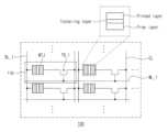
도 1은 본 발명의 일 실시예에 따른 프로세싱 인 메모리 장치를 도시한 것이다.FIG. 1 illustrates a processing-in-memory device according to one embodiment of the present invention.
도 1을 참조하면, 프로세싱 인 메모리 장치(10)는 입력 데이터에 대한 MAC(Multiply ACcumulation) 연산을 수행한다. 예를 들어, MAC 연산은 입력 데이터()와 가중치()에 대하여으로 정의될 수 있다. 여기서, j 및 k는 인덱스이고,는 MAC 연산의 결과이다.Referring to Fig. 1, the processing-in-memory device (10) performs a MAC (Multiply ACcumulation) operation on input data. For example, the MAC operation may be performed on input data ( ) and weights ( ) About can be defined as, where j and k are indices, is the result of MAC operation.
프로세싱 인 메모리 장치(10)는 MAC 연산을 수행하기 위하여 가중치 저장 어레이(100), 곱 연산 어레이(200), 합 연산 어레이(300) 및 주변 회로(400)를 포함한다.The processing-in-memory device (10) includes a weight storage array (100), a product operation array (200), a sum operation array (300), and peripheral circuits (400) to perform a MAC operation.
가중치 저장 어레이(100), 곱 연산 어레이(200), 합 연산 어레이(300)는 계산 라인(CL)을 통해 서로 연결된다.The weight storage array (100), the product operation array (200), and the sum operation array (300) are connected to each other through a calculation line (CL).
가중치 저장 어레이(100)는 복수의 가중치 저장 셀(110)을 포함하며, 각각의 가중치 저장 셀(110)은 가중치를 저장한다. 저장된 가중치는 계산 라인(CL)을 통해 곱 연산 어레이(200)로 인가된다.The weight storage array (100) includes a plurality of weight storage cells (110), and each weight storage cell (110) stores a weight. The stored weight is applied to the multiplication operation array (200) through a calculation line (CL).
곱 연산 어레이(200)는 복수의 곱 연산 셀(210)을 포함하며, 가중치 저장 어레이(100)와 연결되어 가중치를 읽고, 가중치와 입력 데이터 간에 곱 연산을 수행한다. 복수의 곱 연산 셀(210) 각각은 곱 연산에 따른 곱 연산의 결과를 저장한다. 곱 연산의 결과는 계산 라인(CL)을 통해 합 연산 어레이(300)로 인가된다.The multiplication operation array (200) includes a plurality of multiplication operation cells (210), and is connected to the weight storage array (100) to read weights and perform a multiplication operation between the weights and input data. Each of the plurality of multiplication operation cells (210) stores the result of the multiplication operation according to the multiplication operation. The result of the multiplication operation is applied to the sum operation array (300) through the calculation line (CL).
합 연산 어레이(300)는 곱 연산 어레이(200)와 연결되어 곱 연산의 결과를 읽고, 곱 연산의 결과에 대한 합 연산을 수행한다. 구체적으로, 합 연산 어레이(300)는 복수의 곱 연산 셀(210) 중 적어도 두 개의 곱 연산 셀(210)로부터 복수의 곱 연산의 결과를 읽고 복수의 곱 연산의 결과를 합하는 합 연산을 수행한다.The sum operation array (300) is connected to the multiplication operation array (200), reads the results of the multiplication operation, and performs a sum operation on the results of the multiplication operation. Specifically, the sum operation array (300) reads the results of the multiple multiplication operations from at least two of the multiple multiplication operation cells (210) and performs a sum operation that adds the results of the multiple multiplication operations.
주변 회로(400)는 상술한 가중치 저장 어레이(100), 곱 연산 어레이(200) 및 합 연산 어레이(300)를 제어한다. 주변 회로(400)는 제1 워드 라인 내지 제3 워드 라인 드라이버(410, 420, 440) 및 전압 인가 드라이버(430)를 포함한다.The peripheral circuit (400) controls the weight storage array (100), the multiplication operation array (200), and the sum operation array (300) described above. The peripheral circuit (400) includes first to third word line drivers (410, 420, 440) and a voltage application driver (430).
각각이 자화 방향에 따라 결정된 저항을 갖는 MTJ(Magnetic Tunnel Junction) 소자를 포함하고, 저항에 따라 논리 값 중 하나를 갖는 제1 입력 신호가 비트 라인을 통해 인가되는 복수의 가중치 저장 셀(110)을 포함한다.Each of the weight storage cells (110) includes a magnetic tunnel junction (MTJ) element having a resistance determined according to a magnetization direction, and a first input signal having one of the logic values according to the resistance is applied through a bit line.
주변 회로(400)는 제1 워드 라인 드라이버(410) 내지 제3 워드 라인 드라이버(440) 및 전압 인가 드라이버(430)를 포함한다.The peripheral circuit (400) includes a first word line driver (410) to a third word line driver (440) and a voltage application driver (430).
제1 워드 라인 드라이버(410)는 가중치 저장 어레이(100)와 제1 워드 라인(WL_1)을 통해 연결되며, 제1 워드 라인(WL_1)에 인가되는 신호를 제어한다. 제2 워드 라인 드라이버(420)는 곱 연산 어레이(200)와 제2-1 워드 라인(WL_2-1) 및 제2-2 워드 라인(WL_2-2)을 통해 연결되며, 제2-1 워드 라인(WL_2-1) 및 제2-2 워드 라인(WL_2-2)에 인가되는 신호를 제어한다. 제3 워드 라인 드라이버(440)는 합 연산 어레이(300)와 제3-1 워드 라인(WL_3-1) 및 제3-2 워드 라인(WL_3-2)을 통해 연결되며, 제3-1 워드 라인(WL_3-1) 및 제3-2 워드 라인(WL_3-2)에 인가되는 신호를 제어한다. 전압 인가 드라이버(430)는 후술할 제2 비트 라인(BL_2)을 통해 곱 연산 어레이(200)에 제2 입력 신호를 인가한다.The first word line driver (410) is connected to the weight storage array (100) through the first word line (WL_1) and controls a signal applied to the first word line (WL_1). The second word line driver (420) is connected to the multiplication operation array (200) through the second-first word line (WL_2-1) and the second-second word line (WL_2-2), and controls a signal applied to the second-first word line (WL_2-1) and the second-second word line (WL_2-2). The third word line driver (440) is connected to the sum operation array (300) through the third-first word line (WL_3-1) and the third-second word line (WL_3-2), and controls signals applied to the third-first word line (WL_3-1) and the third-second word line (WL_3-2). The voltage application driver (430) applies a second input signal to the multiplication operation array (200) through the second bit line (BL_2) described later.
이하에서는, 가중치 저장 어레이(100), 곱 연산 어레이(200) 및 합 연산 어레이(300)에 대하여 보다 구체적으로 설명한다.Below, the weight storage array (100), the product operation array (200), and the sum operation array (300) are described in more detail.
도 2는 본 발명의 일 실시예에 따른 가중치 저장 어레이를 도시한 것이다.FIG. 2 illustrates a weight storage array according to one embodiment of the present invention.
도 2를 참조하면, 가중치 저장 어레이(100)는 복수의 가중치 저장 셀(110)을 포함한다. 복수의 가중치 저장 셀(110)은 행(row) 방향으로 제1 워드 라인(WL_1)과 연결되고, 열(column) 방향으로 제1 비트 라인(BL_1) 및 계산 라인(CL)과 연결된다. 복수의 가중치 저장 셀(110)은 각각이 자화 방향에 따라 결정된 저항을 갖는 MTJ(Magnetic Tunnel Junction) 소자를 포함하고, 저항에 따라 논리 값 중 하나를 갖는 제1 입력 신호가 제1 비트 라인(BL_1)을 통해 인가된다.Referring to FIG. 2, the weight storage array (100) includes a plurality of weight storage cells (110). The plurality of weight storage cells (110) are connected to a first word line (WL_1) in a row direction, and are connected to a first bit line (BL_1) and a calculation line (CL) in a column direction. Each of the plurality of weight storage cells (110) includes a magnetic tunnel junction (MTJ) element having a resistance determined according to a magnetization direction, and a first input signal having one of the logic values according to the resistance is applied through the first bit line (BL_1).
MTJ 소자(MTJ)는 도시된 바와 같이 자유층(free layer)과 고정층(pinned layer) 사이에 터널 장벽(tunneling barrier)이 구비되는 구조를 갖는다. 자유층과 고정층은 금속층(예를 들어, 강자성체 등)으로 형성되고 터널 장벽은 절연체로 형성될 수 있다. 이때, 자유층은 자화 방향이 바뀔 수 있는 층이고 고정층은 자화 방향이 고정된 층이다. 자유층과 고정층의 자화 방향이 동일한 경우(즉 평행인 경우) MTJ 소자(MTJ)는 낮은 저항을 나타내고, 자화 방향이 다른 경우(즉 반평행인 경우) MTJ 소자(MTJ)는 높은 저항을 나타낸다. 복수의 가중치 저장 셀(110) 각각에 포함된 MTJ 소자(MTJ)는 상술한 바와 같이 자화 방향에 따라 낮은 저항 또는 높은 저항을 나타내며, 이는 곧 논리 값('1' 또는 '0')에 대응될 수 있다. 따라서, 가중치 저장 셀(110) 각각은 MTJ 소자(MTJ)에 따라 논리 값을 저장하며, MTJ 소자(MTJ)의 저항의 크기에 따라 제1 입력 신호의 크기가 결정된다. 제1 입력 신호의 크기도 마찬가지로 논리 값에 대응될 수 있고, 이에 따라 상술한 가중치에 대응될 수 있다.The MTJ element (MTJ) has a structure in which a tunneling barrier is provided between a free layer and a pinned layer, as illustrated. The free layer and the pinned layer may be formed of a metal layer (for example, a ferromagnetic material, etc.), and the tunneling barrier may be formed of an insulator. At this time, the free layer is a layer whose magnetization direction can be changed, and the pinned layer is a layer whose magnetization direction is fixed. When the magnetization directions of the free layer and the pinned layer are the same (i.e., parallel), the MTJ element (MTJ) exhibits low resistance, and when the magnetization directions are different (i.e., antiparallel), the MTJ element (MTJ) exhibits high resistance. The MTJ element (MTJ) included in each of the plurality of weight storage cells (110) exhibits low resistance or high resistance depending on the magnetization direction, as described above, and this may correspond to a logic value ('1' or '0'). Accordingly, each of the weight storage cells (110) stores a logic value according to the MTJ element (MTJ), and the size of the first input signal is determined according to the size of the resistance of the MTJ element (MTJ). The size of the first input signal can also correspond to the logic value, and thus can correspond to the weight described above.
복수의 가중치 저장 셀(110)은 제1 비트 라인(BL_1)에 연결된 MTJ 소자(MTJ)와 제1 트랜지스터를 포함한다. 제1 트랜지스터는 게이트가 제1 워드 라인(WL_1)에 연결되고, 제1 워드 라인(WL_1)에 따라 MTJ 소자(MTJ)와 계산 라인(CL)을 연결한다. 제1 트랜지스터는 제1 워드 라인(WL_1)에 인가되는 신호에 따라 온(on)된다.A plurality of weight storage cells (110) include a MTJ element (MTJ) connected to a first bit line (BL_1) and a first transistor. The first transistor has a gate connected to a first word line (WL_1) and connects the MTJ element (MTJ) and a calculation line (CL) according to the first word line (WL_1). The first transistor is turned on according to a signal applied to the first word line (WL_1).
가중치 저장 어레이(100)는 제1 비트 라인(BL_1)을 통해 제1 입력 신호가 인가될 경우, 제1 워드 라인(WL_1)에 의해 복수의 가중치 저장 셀(110) 중 적어도 하나의 행이 선택되며, 선택된 적어도 하나의 행은 제1 트랜지스터가 온 됨에 따라 제1 입력 신호를 계산 라인(CL)을 통해 곱 연산 어레이(200)로 인가한다.When a first input signal is applied to the weight storage array (100) through the first bit line (BL_1), at least one row among a plurality of weight storage cells (110) is selected by the first word line (WL_1), and the selected at least one row applies the first input signal to the multiplication operation array (200) through the calculation line (CL) as the first transistor is turned on.
도 3은 본 발명의 일 실시예에 따른 곱 연산 어레이를 도시한 것이다.FIG. 3 illustrates a multiplication operation array according to one embodiment of the present invention.
도 3을 참조하면, 곱 연산 어레이(200)는 복수의 곱 연산 셀(210)을 포함한다. 복수의 곱 연산 셀(210)은 행 방향으로 제2 비트 라인(BL_2), 제2-1 워드 라인(WL_2-1) 및 제2-2 워드 라인(WL_2-2)과 연결되고, 열 방향으로 계산 라인(CL)과 연결된다. 복수의 곱 연산 셀(210)은 각각이 제1 SOT(Spin Orbit Torque) 소자를 포함하고, 복수의 가중치 저장 셀(110) 중 적어도 하나의 가중치 저장 셀(110)로부터 제1 입력 신호를 읽고, 제1 입력 신호와 제2 비트 라인(BL_2)을 통해 인가되는 제2 입력 신호의 곱 연산을 수행한다.Referring to FIG. 3, the multiplication operation array (200) includes a plurality of multiplication operation cells (210). The plurality of multiplication operation cells (210) are connected to a second bit line (BL_2), a second-first word line (WL_2-1), and a second-second word line (WL_2-2) in the row direction, and are connected to a calculation line (CL) in the column direction. Each of the plurality of multiplication operation cells (210) includes a first SOT (Spin Orbit Torque) element, reads a first input signal from at least one weight storage cell (110) among the plurality of weight storage cells (110), and performs a multiplication operation between the first input signal and a second input signal applied through the second bit line (BL_2).
SOT 소자는 도시된 바와 같이 상술한 MTJ 소자(MTJ)에 헤비 메탈(heavy metal)이 결합된 구조를 갖는다. SOT 소자의 헤비 메탈에는 쓰기 전류가 흐를 수 있는데, 쓰기 전류는 임계 값을 넘는 크기를 가지면 전류 방향이 스위칭될 수 있다. 쓰기 전류의 전류 방향을 스위칭하는 임계 값은 SOT 소자의 고정층에 인가되는 전압(VMTJ)에 따라 조절될 수 있다. 또한, 쓰기 전류의 전류 방향에 따라 MTJ 소자(MTJ)의 저항의 크기(높은 저항 또는 낮은 저항)가 결정된다.The SOT device has a structure in which a heavy metal is combined with the MTJ device (MTJ) described above, as illustrated. A write current can flow through the heavy metal of the SOT device, and the current direction can be switched when the write current has a magnitude exceeding a threshold value. The threshold value for switching the current direction of the write current can be adjusted according to the voltage (VMTJ ) applied to the fixed layer of the SOT device. In addition, the resistance size (high resistance or low resistance) of the MTJ device (MTJ) is determined according to the current direction of the write current.
복수의 곱 연산 셀(210)은 제1 SOT 소자(SOT_1), 제2-1 트랜지스터(TR_2-1) 및 제2-2 트랜지스터(TR_2-2)를 포함한다.The multiple multiplication operation cell (210) includes a first SOT element (SOT_1), a second-first transistor (TR_2-1), and a second-second transistor (TR_2-2).
제1 SOT 소자(SOT_1)는 계산 라인(CL)으로부터 제1 입력 신호를 인가받는다. 예를 들어, 제1 SOT 소자(SOT_1)의 헤비 메탈은 도시된 바와 같이 별도의 트랜지스터를 통해 계산 라인(CL)과 연결되어 제1 입력 신호를 인가받을 수 있다.The first SOT element (SOT_1) receives a first input signal from the calculation line (CL). For example, the heavy metal of the first SOT element (SOT_1) may be connected to the calculation line (CL) through a separate transistor as illustrated to receive the first input signal.
제2-1 트랜지스터(TR_2-1)는 게이트가 제2-1 워드 라인(WL_2-1)에 연결되고, 제2-1 워드 라인(WL_2-1)에 따라 제2 비트 라인(BL_2)과 제1 SOT 소자(SOT_1)를 연결한다. 제2-1 트랜지스터(TR_2-1)는 제2-1 워드 라인(WL_2-1)에 인가되는 신호에 따라 온된다. 제2-1 트랜지스터(TR_2-1)가 온될 경우, 제2 입력 신호가 제2 비트 라인(BL_2)을 통해 제1 SOT 소자(SOT_1)에 인가된다. 여기서, 제2 입력 신호는 VMTJ에 대응될 수 있고, VMTJ의 크기에 따라 논리 값을 갖는다.The second-first transistor (TR_2-1) has a gate connected to the second-first word line (WL_2-1) and connects the second bit line (BL_2) and the first SOT element (SOT_1) according to the second-first word line (WL_2-1). The second-first transistor (TR_2-1) is turned on according to a signal applied to the second-first word line (WL_2-1). When the second-first transistor (TR_2-1) is turned on, a second input signal is applied to the first SOT element (SOT_1) through the second bit line (BL_2). Here, the second input signal can correspond to VMTJ and has a logic value according to the size of VMTJ .
제2-2 트랜지스터(TR_2-2)는 게이트가 제2-2 워드 라인(WL_2-2)에 연결되고, 제2-2 워드 라인(WL_2-2)에 따라 제1 SOT 소자(SOT_1)와 계산 라인(CL)을 연결한다. 제2-2 트랜지스터(TR_2-2)는 제2-2 워드 라인(WL_2-2)에 인가되는 신호에 따라 온된다. 제2-2 트랜지스터(TR_2-2)가 온될 경우, 제1 SOT 소자(SOT_1)를 흐르는 전류가 계산 라인(CL)에 전달된다.The second-second transistor (TR_2-2) has a gate connected to the second-second word line (WL_2-2) and connects the first SOT element (SOT_1) and the calculation line (CL) according to the second-second word line (WL_2-2). The second-second transistor (TR_2-2) is turned on according to a signal applied to the second-second word line (WL_2-2). When the second-second transistor (TR_2-2) is turned on, the current flowing through the first SOT element (SOT_1) is transferred to the calculation line (CL).
곱 연산 어레이(200)는 상술한 가중치 저장 셀(110)에 기초하여 복수의 가중치 저장 셀(110) 중 적어도 하나의 가중치 저장 셀(110)로부터 제1 입력 신호를 읽고, 제1 입력 신호와 제2 비트 라인(BL_2)을 통해 인가되는 제2 입력 신호의 곱 연산을 수행한다.The multiplication operation array (200) reads a first input signal from at least one weight storage cell (110) among a plurality of weight storage cells (110) based on the above-described weight storage cells (110), and performs a multiplication operation of the first input signal and a second input signal applied through the second bit line (BL_2).
도 4는 곱 연산 동작을 설명하기 위한 것이다.Figure 4 is for explaining the multiplication operation operation.
도 4를 참조하면, 가중치 저장 어레이(100)는 제1 입력 신호를 곱 연산 어레이(200)로 인가하는데, 이때 제1 입력 신호는 MTJ 소자(MTJ)가 갖는 자화 방향에 따라 달라지는 저항에 따른 크기를 갖는다. 제1 입력 신호는 곱 연산 어레이(200)의 열에 동시에 인가되어 공유될 수 있다. 열에 포함된 SOT 소자의 각 출력은 제1 입력 신호와 제2 입력 신호를 아래 표 1과 같이 NAND(또는 AND) 연산하는 것에 기초하여 곱 연산을 수행한다.Referring to FIG. 4, the weight storage array (100) applies a first input signal to the multiplication operation array (200), wherein the first input signal has a size according to the resistance that varies depending on the magnetization direction of the MTJ element (MTJ). The first input signal can be simultaneously applied to the columns of the multiplication operation array (200) and shared. Each output of the SOT element included in the column performs a multiplication operation based on performing a NAND (or AND) operation on the first input signal and the second input signal as shown in Table 1 below.
표 1과 같이, 제1 입력 신호와 제2 입력 신호의 논리 값이 모두 '1'인 경우에만 곱 연산의 결과 신호의 논리 값이 '0(만약 AND인 경우 1)'이고, 그 외의 경우는 '1'로 출력되므로 곱 연산이 수행될 수 있다. 이러한 NAND 기반의 곱 연산은 상술한 바와 같이 제1 입력 신호가 공유되므로 병렬로 수행 가능하다.As shown in Table 1, the logic value of the result signal of the multiplication operation is '0 (1 if AND)' only when the logic values of the first input signal and the second input signal are both '1', and in other cases, it is output as '1', so the multiplication operation can be performed. This NAND-based multiplication operation can be performed in parallel because the first input signal is shared as described above.
도 4의 경우를 예로 들면, 가중치 저장 어레이(100)의 MTJ 소자(MTJ)의 저항의 크기를 가중치(W[m], 여기서 m은 가중치 인덱스)라 하면, 제1 입력 신호(IN1)은 MTJ 소자(MTJ)를 통해 곱 연산 어레이(200)에 IW(W[m])의 형태로 인가되고, 곱 연산 어레이(200)의 열에 포함된 SOT 소자 각각에는 제2 입력 신호(VG0(I[n]), VG0(I[n+1]))가 인가된다. 만약 제1 입력 신호의 크기가 충분하고 제2 입력 신호에 따라 SOT 소자의 임계 값이 낮아져서 SOT 소자의 헤비 메탈을 흐르는 신호, 즉 곱 연산의 결과 신호의 방향이 스위칭될 경우에는 논리 값 '0'을 갖고, 스위칭되지 않을 경우 논리 값 '1'을 가질 수 있다.Taking the case of Fig. 4 as an example, if the size of the resistance of the MTJ element (MTJ) of the weight storage array (100) is referred to as a weight (W[m], where m is a weight index), the first input signal (IN1) is applied in the form of IW (W[m]) to the multiplication operation array (200) through the MTJ element (MTJ), and the second input signal (VG0 (I[n]), VG0 (I[n+1])) is applied to each of the SOT elements included in the column of the multiplication operation array (200). If the size of the first input signal is sufficient and the threshold value of the SOT element is lowered according to the second input signal, the direction of the signal flowing through the heavy metal of the SOT element, i.e., the result signal of the multiplication operation, is switched, and if not switched, it can have a logic value of '0'.
곱 연산 어레이(200)는 상술한 바와 같이 제1 입력 신호의 크기 및 제2 입력 신호의 크기에 따라 제1 SOT 소자(SOT_1)를 흐르는 제1 입력 신호의 방향이 스위칭 되는 것에 기초하여 곱 연산을 수행하고, 곱 연산의 결과 신호는 제1 입력 신호의 방향이 스위칭 되는지 여부에 따라 논리 값을 가질 수 있다.The multiplication operation array (200) performs a multiplication operation based on the switching of the direction of the first input signal flowing through the first SOT element (SOT_1) according to the magnitude of the first input signal and the magnitude of the second input signal as described above, and the result signal of the multiplication operation can have a logic value depending on whether the direction of the first input signal is switched.
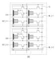
도 5는 본 발명의 일 실시예에 따른 합 연산 어레이를 도시한 것이다.FIG. 5 illustrates a sum operation array according to one embodiment of the present invention.
도 5를 참조하면, 합 연산 어레이(300)는 복수의 캐리 셀(310) 및 복수의 섬 셀(320)을 포함한다. 복수의 캐리 셀(310)과 복수의 섬 셀(320)은 계산 라인(CL)을 통해 연결된다.Referring to FIG. 5, the sum operation array (300) includes a plurality of carry cells (310) and a plurality of island cells (320). The plurality of carry cells (310) and the plurality of island cells (320) are connected through a calculation line (CL).
복수의 캐리 셀(310)은 제2-2 트랜지스터(TR_2-2)가 온 됨에 따라 계산 라인(CL)을 통해 복수의 곱 연산 셀(210) 중 적어도 하나의 곱 연산 셀(210)로부터 곱 연산의 결과 신호를 인가받고, 곱 연산의 결과 신호의 합 연산에 대한 캐리(carry) 신호를 저장한다.A plurality of carry cells (310) receive a result signal of a multiplication operation from at least one of the plurality of multiplication operation cells (210) through a calculation line (CL) when the 2-2 transistor (TR_2-2) is turned on, and store a carry signal for a sum operation of the result signal of the multiplication operation.
복수의 캐리 셀(310) 각각은 적어도 하나의 제2-1 SOT 소자(SOT_2-1) 및 적어도 하나의 제3-1 트랜지스터를 포함한다. 도 5의 경우 적어도 하나의 제2-1 SOT 소자(SOT_2-1) 및 적어도 하나의 제3-1 트랜지스터가 각각 2개인 것으로 도시되었으나, 설계에 따라 그 개수가 달라질 수 있음은 당연하다.Each of the plurality of carry cells (310) includes at least one 2-1 SOT element (SOT_2-1) and at least one 3-1 transistor. In the case of FIG. 5, at least one 2-1 SOT element (SOT_2-1) and at least one 3-1 transistor are illustrated as two each, but it is obvious that the number may vary depending on the design.
적어도 하나의 제2-1 소자는 계산 라인(CL)으로부터 곱 연산의 결과 신호를 인가받는다. 적어도 하나의 제2-1 소자 각각의 헤비 메탈은 서로 직렬로 연결되어 동일한 전류가 흐른다.At least one 2-1 element receives a result signal of a multiplication operation from a calculation line (CL). The heavy metals of each of the at least one 2-1 elements are connected in series with each other so that the same current flows.
적어도 하나의 제3-1 트랜지스터는 게이트가 적어도 하나의 제3-1 워드 라인(WL_3-1)에 연결되고, 적어도 하나의 제3-1 워드 라인(WL_3-1)에 따라 적어도 하나의 제2-1 SOT 소자(SOT_2-1)와 계산 라인(CL)을 연결한다. 적어도 하나의 제3-1 트랜지스터는 적어도 하나의 제3-1 워드 라인(WL_3-1)에 인가되는 신호에 따라 온되어 캐리 신호를 계산 라인(CL)에 인가한다.At least one 3-1th transistor has a gate connected to at least one 3-1th word line (WL_3-1) and connects at least one 2-1th SOT element (SOT_2-1) and a compute line (CL) according to at least one 3-1th word line (WL_3-1). At least one 3-1th transistor is turned on according to a signal applied to at least one 3-1th word line (WL_3-1) to apply a carry signal to the compute line (CL).
복수의 섬 셀(320)은 곱 연산의 결과 신호의 합 연산을 수행하고, 합 연산에 대한 섬(sum) 신호를 저장한다.A plurality of island cells (320) perform a sum operation on the result signal of the multiplication operation and store a sum signal for the sum operation.
복수의 섬 셀(320) 각각은 제2-2 SOT 소자(SOT_2-2) 및 제3-2 트랜지스터를 포함한다.Each of the plurality of island cells (320) includes a 2-2 SOT element (SOT_2-2) and a 3-2 transistor.
제2-2 SOT 소자(SOT_2-2)는 곱 연산의 결과 신호 및 캐리 신호를 계산 라인(CL)을 통해 인가받는다.The 2-2 SOT element (SOT_2-2) receives the result signal of the multiplication operation and the carry signal through the calculation line (CL).
제3-2 트랜지스터는 게이트가 제3-2 워드 라인(WL_3-2)에 연결되고, 제3-2 워드 라인(WL_3-2)에 따라 제2-2 SOT 소자(SOT_2-2)와 계산 라인(CL)을 연결한다. 제3-2 트랜지스터는 제3-2 워드 라인(WL_3-2)에 인가되는 신호에 따라 온되어 섬 신호를 계산 라인(CL)에 인가한다.The third-2 transistor has its gate connected to the third-2 word line (WL_3-2) and connects the second-2 SOT element (SOT_2-2) and the compute line (CL) according to the third-2 word line (WL_3-2). The third-2 transistor is turned on according to a signal applied to the third-2 word line (WL_3-2) and applies an island signal to the compute line (CL).
도 6a 및 도 6b는 합 연산 동작을 설명하기 위한 것이다.Figures 6a and 6b are for explaining the sum operation operation.
도 6a를 참조하면, 우선 복수의 캐리 셀(310) 각각은 곱 연산 어레이(200)로부터 곱 연산의 결과 신호(IN)를 계산 라인(CL)을 통해 인가받는다. 이때, 복수의 캐리 셀(310)은 복수의 곱 연산 셀(210) 중 적어도 하나의 곱 연산 셀(210)로부터 곱 연산의 결과 신호를 계산 라인(CL)을 통해 읽으며, 적어도 하나의 곱 연산 셀(210)이 복수인 경우 복수의 곱 연산의 결과 신호가 누적된 누적 신호를 읽게 된다.Referring to FIG. 6A, first, each of the plurality of carry cells (310) receives a result signal (IN) of a multiplication operation from the multiplication operation array (200) through a calculation line (CL). At this time, the plurality of carry cells (310) read a result signal of a multiplication operation from at least one of the plurality of multiplication operation cells (210) through the calculation line (CL), and when there are multiple at least one multiplication operation cells (210), an accumulated signal in which result signals of the plurality of multiplication operations are accumulated is read.
복수의 곱 연산의 결과 신호는 적어도 하나의 제2-1 SOT 소자(SOT_2-1)(구체적으로는 헤비 메탈)를 흐르게 되는데, 이때 복수의 곱 연산의 결과 신호가 누적된 크기에 따라 적어도 하나의 제2-1 SOT 소자(SOT_2-1)를 흐르는 누적 신호(Imaj3)의 방향이 스위칭될 수 있다. 따라서, 복수의 캐리 셀(310)은 적어도 하나의 제2-1 SOT 소자(SOT_2-1)를 흐르는 곱 연산의 결과 신호의 크기에 따라 곱 연산의 결과 신호의 방향이 스위칭 되는 것에 기초하여 캐리 신호(OUT)를 저장한다.The result signal of the multiple multiplication operations flows through at least one 2-1 SOT element (SOT_2-1) (specifically, a heavy metal), and at this time, the direction of the accumulation signal (Imaj3 ) flowing through at least one 2-1 SOT element (SOT_2-1) can be switched according to the accumulated size of the result signal of the multiple multiplication operations. Accordingly, the plurality of carry cells (310) store the carry signal (OUT) based on the switching of the direction of the result signal of the multiplication operation according to the size of the result signal of the multiplication operation flowing through at least one 2-1 SOT element (SOT_2-1).
도 6b를 참조하면, 복수의 섬 셀(320) 각각은 복수의 곱 연산 셀(210) 중 적어도 하나의 곱 연산 셀(210) 및 캐리 셀(310)로부터 계산 라인(CL)을 통해 곱 연산의 결과 신호 및 캐리 신호의 누적 신호(Imaj5)를 읽는다.Referring to FIG. 6b, each of the plurality of island cells (320) reads the result signal of the multiplication operation and the accumulation signal (Imaj5 ) of the carry signal from at least one of the plurality of multiplication operation cells (210) and the carry cell (310) through the calculation line (CL).
누적 신호는 제2-2 SOT 소자(SOT_2-2)(구체적으로는 헤비 메탈)를 흐르게 되는데, 이때 누적 신호의 크기에 따라 제2-2 SOT 소자(SOT_2-2)를 흐르는 누적 신호(Imaj5)의 방향이 스위칭될 수 있다. 따라서, 복수의 섬 셀(320)은 제2-2 SOT 소자(SOT_2-2)를 흐르는 연산의 결과 신호 및 캐리 신호의 누적 신호의 크기에 따라 누적 신호의 방향이 스위칭 되는 것에 기초하여 섬 신호를 저장한다.The accumulation signal flows through the 2nd SOT element (SOT_2-2) (specifically, a heavy metal), and at this time, the direction of the accumulation signal (Imaj5 ) flowing through the 2nd SOT element (SOT_2-2) can be switched depending on the size of the accumulation signal. Accordingly, the plurality of island cells (320) store the island signal based on the switching of the direction of the accumulation signal depending on the size of the accumulation signal of the operation result signal and the carry signal flowing through the 2nd SOT element (SOT_2-2).
합 연산 어레이(300)는 상술한 바와 같이 곱 연산의 결과 신호에 대하여 전가산기(full adder) 로직 게이트 기반의 합 연산을 캐리 신호 및 섬 신호를 통해 수행할 수 있다. 특히, 캐리 신호 생성 시 복수의 SOT 소자에서 전류를 공유하는 구조를 가지므로 연산에 2단계만 필요하다는 이점이 있다.As described above, the sum operation array (300) can perform a sum operation based on a full adder logic gate on the result signal of the multiplication operation through a carry signal and an island signal. In particular, since it has a structure in which current is shared among multiple SOT elements when generating a carry signal, there is an advantage in that only two steps are required for the operation.
이하에서는, 상술한 가중치 저장 어레이(100), 곱 연산 어레이(200) 및 합 연산 어레이(300)에 기초한 프로세싱 인 메모리 장치(10)의 전체적인 동작을 설명한다.Below, the overall operation of the processing-in-memory device (10) based on the above-described weight storage array (100), product operation array (200), and sum operation array (300) is described.
도 7a 내지 도 7c는 본 발명의 일 실시예에 따른 프로세싱 인 메모리 장치(10)의 동작을 설명하기 위한 것이다.FIGS. 7A to 7C are for explaining the operation of a processing-in-memory device (10) according to one embodiment of the present invention.
도 7a 내지 도 7c에 도시된 파라미터에 대하여 설명하면, W(i-index),(o-index),(bit)는 가중치, I(i-index),(bit)는 제2 입력 신호, PP(i-index),(o-index),(bit),(W-bit)는 곱 연산의 결과 신호, C(i-index),(o-index),(bit),(W-bit)는 캐리 신호, S(i-index),(o-index),(bit),(W-bit)는 섬 신호를 의미하며, i-index 및 o-index는 MAC 연산의 입/출력 데이터의 인덱스, bit는 이진 값, W-bit는 가중치의 이진 값을 나타낸다.With respect to the parameters illustrated in FIGS. 7a to 7c, W(i-index), (o-index), (bit) represents a weight, I(i-index), (bit) represents a second input signal, PP(i-index), (o-index), (bit), (W-bit) represents a result signal of a multiplication operation, C(i-index), (o-index), (bit), (W-bit) represents a carry signal, and S(i-index), (o-index), (bit), (W-bit) represents an island signal. i-index and o-index represent indices of input/output data of a MAC operation, bit represents a binary value, and W-bit represents a binary value of a weight.
도 7a를 참조하면, PP의 생성은 첫 번째 주기(1st cycle)부터 N번째 주기(Nth cycle)까지 각각 수행되며, 각 주기는 가중치 저장 어레이(100) 및 곱 연산 어레이(200)의 각 행에 대응될 수 있다.Referring to FIG. 7a, the generation of PP is performed from the first cycle (1st cycle) to the Nth cycle, and each cycle can correspond to each row of the weight storage array (100) and the product operation array (200).
가중치 저장 어레이(100)에 저장된 가중치 W(i-index),(o-index),(bit)에 따라 제1 입력 신호가 계산 라인(CL)을 통해 곱 연산 어레이(200)로 인가된다. 곱 연산 어레이(200)는 제1 입력 신호와 제2 입력 신호를 읽고, 곱 연산을 수행한다.According to the weights W(i-index), (o-index), (bit) stored in the weight storage array (100), the first input signal is applied to the multiplication operation array (200) through the calculation line (CL). The multiplication operation array (200) reads the first input signal and the second input signal and performs a multiplication operation.
도 7b를 참조하면, 곱 연산이 수행된 후 합 연산이 수행된다. 곱 연산 어레이(200)의 곱 연산에 따른 곱 연산의 결과 신호가 합 연산 어레이(300), 구체적으로는 캐리 셀(310)에 인가되며, 캐리 셀(310)은 캐리 신호를 생성한다.Referring to Fig. 7b, a sum operation is performed after a multiplication operation is performed. A result signal of a multiplication operation according to the multiplication operation of the multiplication operation array (200) is applied to a sum operation array (300), specifically, a carry cell (310), and the carry cell (310) generates a carry signal.
이후, 곱 연산의 결과 신호 및 캐리 신호가 섬 셀(320)로 인가되며, 섬 셀(320)은 섬 신호를 생성한다. 합 연산은 합 연산 어레이(300)의 행에 대하여 공통적으로 수행될 수 있다.Thereafter, the result signal of the multiplication operation and the carry signal are applied to the island cell (320), and the island cell (320) generates an island signal. The sum operation can be commonly performed for the rows of the sum operation array (300).
도 7c를 참조하면, 합 연산은 반복적으로 수행될 수 있다. 일 실시예에 따르면, 합 연산 어레이(300)는 행 방향을 따라 캐리 셀(310)과 섬 셀(320)이 교대로 연결되는 구조를 가질 수 있으며, 하나의 캐리 셀(310)과 섬 셀(320)이 결합된 셀을 단위 셀(330)로 칭할 경우 단위 셀(330)이 행을 따라 순차적으로 연결되는 구조를 가질 수 있다. 각 단위 셀(330)은 특정 단위(예를 들어, 도 7c에서는 3개)의 입력 데이터에 대한 곱 연산의 결과 신호를 합 연산할 수 있다.Referring to FIG. 7c, the sum operation can be performed repeatedly. According to one embodiment, the sum operation array (300) can have a structure in which carry cells (310) and island cells (320) are alternately connected along the row direction, and when a cell in which one carry cell (310) and an island cell (320) are combined is called a unit cell (330), the unit cells (330) can have a structure in which they are sequentially connected along the row. Each unit cell (330) can perform a sum operation on a result signal of a multiplication operation for input data of a specific unit (for example, three in FIG. 7c).
상술한 바와 같이, 프로세싱 인 메모리 장치(10)에 포함된 가중치 저장 어레이(100), 곱 연산 어레이(200) 및 합 연산 어레이(300)는 계산 라인(CL)을 통해 연결되어 MAC 연산을 수행할 수 있다. 특히, 계산 라인(CL)은 가중치 저장 어레이(100), 곱 연산 어레이(200) 및 합 연산 어레이(300)의 열 라인을 정의하고, 가중치 저장 어레이(100), 곱 연산 어레이(200) 및 합 연산 어레이(300)는 MAC 연산을 이러한 열 라인에서 동시에 수행할 수 있어 연산에 이점을 가진다.As described above, the weight storage array (100), the product operation array (200), and the sum operation array (300) included in the processing-in-memory device (10) are connected via the calculation line (CL) to perform the MAC operation. In particular, the calculation line (CL) defines the column lines of the weight storage array (100), the product operation array (200), and the sum operation array (300), and the weight storage array (100), the product operation array (200), and the sum operation array (300) can perform the MAC operation simultaneously on these column lines, which has an advantage in the operation.
도 8은 인트라-메모리 어레이 파이프라이닝 구조를 도시한 것이다.Figure 8 illustrates the intra-memory array pipelining structure.
도 8을 참조하면, 상술한 프로세싱 인 메모리 장치(10)에는 인트라-메모리 어레이 파이프라이닝(intra-memory array pipelining) 구조가 적용될 수 있으며, 이에 따라 메모리 장치 더 많은 병렬 연산이 가능할 수 있다.Referring to FIG. 8, the above-described processing-in-memory device (10) may be applied with an intra-memory array pipelining structure, thereby enabling more parallel operations of the memory device.
도 9는 본 발명의 일 실시예에 따른 프로세싱 인 메모리 장치의 동작 방법의 순서도이다. 이하에서는, 상술한 부분과 중복되는 부분에 대한 상세한 설명은 생략한다.Figure 9 is a flowchart of an operation method of a processing-in-memory device according to one embodiment of the present invention. Hereinafter, a detailed description of parts that overlap with those described above will be omitted.
도 9를 참조하면, S110에서, 프로세싱 인 메모리 장치(10)는 가중치 저장 셀(110)을 통해 제1 입력 신호를 곱 연산 어레이(200)로 인가한다. 구체적으로, 가중치 저장 셀(110)은 제1 비트 라인(BL_1)을 통해 제1 입력 신호가 인가될 경우, 제1 워드 라인(WL_1)에 의해 복수의 가중치 저장 셀(110) 중 적어도 하나의 행이 선택되며, 선택된 적어도 하나의 행은 제1 트랜지스터가 온 됨에 따라 제1 입력 신호를 계산 라인(CL)을 통해 곱 연산 어레이(200)로 인가한다.Referring to FIG. 9, in S110, the processing-in-memory device (10) applies a first input signal to the multiplication operation array (200) through the weight storage cell (110). Specifically, when the first input signal is applied to the weight storage cell (110) through the first bit line (BL_1), at least one row among the plurality of weight storage cells (110) is selected by the first word line (WL_1), and the selected at least one row applies the first input signal to the multiplication operation array (200) through the calculation line (CL) as the first transistor is turned on.
S120에서, 프로세싱 인 메모리 장치(10)는 제1 입력 신호와 제2 입력 신호의 곱 연산을 수행한다. 구체적으로, 프로세싱 인 메모리 장치(10)에 포함된 곱 연산 어레이(200)는 제1 입력 신호의 크기 및 제2 입력 신호의 크기에 따라 제1 SOT 소자(SOT_1)를 흐르는 제1 입력 신호의 방향이 스위칭 되는 것에 기초하여 곱 연산을 수행하고, 곱 연산의 결과 신호는 제1 입력 신호의 방향이 스위칭 되는지 여부에 따라 논리 값을 가질 수 있다.In S120, the processing-in-memory device (10) performs a product operation of the first input signal and the second input signal. Specifically, the product operation array (200) included in the processing-in-memory device (10) performs the product operation based on the switching of the direction of the first input signal flowing through the first SOT element (SOT_1) according to the magnitude of the first input signal and the magnitude of the second input signal, and the result signal of the product operation can have a logic value depending on whether the direction of the first input signal is switched.
S130에서, 프로세싱 인 메모리 장치(10)는 곱 연산의 결과 신호에 대한 합 연산을 수행한다. 구체적으로, 프로세싱 인 메모리 장치(10)에 포함된 합 연산 어레이(300)는 곱 연산의 결과 신호에 대하여 전가산기 로직 게이트 기반의 합 연산을 캐리 신호 및 섬 신호를 통해 수행한다.In S130, the processing-in-memory device (10) performs a sum operation on a result signal of a multiplication operation. Specifically, the sum operation array (300) included in the processing-in-memory device (10) performs a full-adder logic gate-based sum operation on a result signal of a multiplication operation through a carry signal and an sum signal.
상술한 본 발명의 다양한 실시예들에 따르면, 메모리 소자로 사용 가능한 스핀 궤도 토크 소자의 전류 스위칭 및 전기장 제어 자기 이방성(Voltage Controlled Magnetic Anisotropy, VCMA) 효과를 이용하여 디지털 로직 게이트를 구성하고, MAC 연산을 수행이 가능한 메모리를 설계하여 메모리와 연산기 간의 데이터 이동 횟수를 줄여 전체 시스템 에너지 효율을 높일 수 있다.According to various embodiments of the present invention described above, a digital logic gate is configured by utilizing the current switching and voltage controlled magnetic anisotropy (VCMA) effects of a spin-orbit torque element usable as a memory element, and a memory capable of performing MAC operations is designed so as to reduce the number of data transfers between the memory and the operator, thereby increasing the energy efficiency of the overall system.
또한, 기존 저항성 소자 기반 PIM에서 사용한 전류 축적을 통한 아날로그 MAC 연산 방식을 디지털 로직 연산을 메모리 내부에서 반복적으로 수행하는 디지털 MAC 방식으로 대체하여 ADC를 제거함으로써 기존에 사용되던 ADC의 면적, 에너지 소모 문제를 해결할 수 있다. 또한, ADC를 제거함으로써 높은 연산량 대비 전력 효율 (TOPS/W)와 연산량 대비 면적 효율 (TOPS/mm2)을 보인다.In addition, the analog MAC operation method through current accumulation used in the existing resistive element-based PIM can be replaced with a digital MAC method that repeatedly performs digital logic operations inside the memory, thereby eliminating the ADC and thus solving the area and energy consumption problems of the existing ADC. In addition, by eliminating the ADC, it shows high power efficiency (TOPS/W) and area efficiency (TOPS/mm2 ) per computational amount.
상술한 설명에서 제안 방식에 대한 일례들 또한 본 발명의 구현 방법들 중 하나로 포함될 수 있으므로, 일종의 제안 방식들로 간주될 수 있음은 명백한 사실이다. 또한, 상기 설명한 제안 방식들은 독립적으로 구현될 수도 있지만, 일부 제안 방식들의 조합 (혹은 병합) 형태로 구현될 수도 있다.It is clear that the examples of the proposed methods in the above description can also be included as one of the implementation methods of the present invention, and thus can be considered as a kind of proposed methods. In addition, the proposed methods described above can be implemented independently, but can also be implemented in the form of a combination (or merge) of some of the proposed methods.
Claims (11)
Translated fromKorean상기 복수의 가중치 저장 셀 중 적어도 하나의 가중치 저장 셀로부터 상기 제1 입력 신호를 읽고, 상기 제1 입력 신호와 전압인가 라인을 통해 인가되는 제2 입력 신호의 곱 연산을 수행하는 복수의 곱 연산 셀을 포함하는 곱 연산 어레이; 및
상기 복수의 곱 연산 셀 중 적어도 하나의 곱 연산 셀로부터 곱 연산의 결과 신호를 읽고, 상기 곱 연산의 결과 신호에 대한 합 연산을 수행하는 복수의 합 연산 셀을 포함하는 합 연산 어레이를 포함하고,
상기 가중치 저장 어레이, 상기 곱 연산 어레이 및 상기 합 연산 어레이는 계산 라인을 통해 연결되어 MAC(Multiply ACcumulation) 연산을 수행하고,
상기 복수의 곱 연산 셀 각각은:
상기 계산 라인으로부터 상기 제1 입력 신호를 인가받는 제1 SOT(Spin Orbit Torque) 소자;
게이트가 제2-1 워드 라인에 연결되고, 상기 제2-1 워드 라인에 따라 상기 전압인가 라인과 상기 제1 SOT 소자를 연결하는 제2-1 트랜지스터; 및
게이트가 제2-2 워드 라인에 연결되고, 상기 제2-2 워드 라인에 따라 상기 제1 SOT 소자와 상기 계산 라인을 연결하는 제2-2 트랜지스터를 포함하고,
상기 합 연산 어레이는:
상기 제2-2 트랜지스터가 온 됨에 따라 상기 계산 라인을 통해 상기 복수의 곱 연산 셀 중 적어도 하나의 곱 연산 셀로부터 상기 곱 연산의 결과 신호를 인가받고, 상기 곱 연산의 결과 신호의 합 연산에 대한 캐리(carry) 신호를 저장하는 복수의 캐리 셀; 및
상기 곱 연산의 결과 신호의 합 연산에 대한 섬(sum) 신호를 저장하는 복수의 섬 셀을 포함하는,
프로세싱 인 메모리 장치.
A weight storage array including a plurality of weight storage cells, each of which includes a magnetic tunnel junction (MTJ) element having a resistance determined according to a magnetization direction, and to which a first input signal having one of the logic values according to the resistance is applied through a bit line;
A multiplication operation array including a plurality of multiplication operation cells that read the first input signal from at least one weight storage cell among the plurality of weight storage cells and perform a multiplication operation of the first input signal and a second input signal applied through a voltage application line; and
A sum operation array including a plurality of sum operation cells that read a result signal of a multiplication operation from at least one of the plurality of multiplication operation cells and perform a sum operation on the result signal of the multiplication operation,
The above weight storage array, the above multiplication operation array and the above sum operation array are connected through a calculation line to perform a MAC (Multiply ACcumulation) operation,
Each of the above multiple multiplication operation cells:
A first SOT (Spin Orbit Torque) element receiving the first input signal from the above calculation line;
A 2-1 transistor having a gate connected to a 2-1 word line and connecting the voltage application line and the first SOT element according to the 2-1 word line; and
A second transistor is included, the gate of which is connected to the second-second word line, and which connects the first SOT element and the calculation line along the second-second word line;
The above sum operation array is:
A plurality of carry cells that receive a result signal of the multiplication operation from at least one of the plurality of multiplication operation cells through the calculation line when the second-2 transistor is turned on, and store a carry signal for a sum operation of the result signal of the multiplication operation; and
Comprising a plurality of island cells storing a sum signal for the sum operation of the result signal of the above multiplication operation,
Processing-in-memory device.
상기 복수의 가중치 저장 셀 각각은:
상기 비트 라인에 연결된 상기 MTJ 소자; 및
게이트가 제1 워드 라인에 연결되고, 상기 제1 워드 라인에 따라 상기 MTJ 소자와 상기 계산 라인을 연결하는 제1 트랜지스터를 포함하는,
프로세싱 인 메모리 장치.
In the first paragraph,
Each of the above multiple weight storage cells:
the MTJ element connected to the bit line; and
A first transistor having a gate connected to a first word line and connecting the MTJ element and the compute line along the first word line,
Processing-in-memory device.
상기 가중치 저장 어레이는,
상기 제1 워드 라인에 의해 상기 복수의 가중치 저장 셀 중 적어도 하나의 행이 선택될 경우, 상기 적어도 하나의 행은 상기 제1 입력 신호를 상기 계산 라인을 통해 상기 곱 연산 어레이로 인가하는,
프로세싱 인 메모리 장치.
In the second paragraph,
The above weight storage array is,
When at least one row of the plurality of weight storage cells is selected by the first word line, the at least one row applies the first input signal to the multiplication operation array through the calculation line.
Processing-in-memory device.
상기 곱 연산 어레이는,
상기 제1 입력 신호의 크기 및 상기 제2 입력 신호의 크기에 따라 상기 제1 SOT 소자를 흐르는 상기 제1 입력 신호의 방향이 스위칭 되는 것에 기초하여 곱 연산을 수행하고,
상기 곱 연산의 결과 신호는 상기 제1 입력 신호의 방향이 스위칭 되는지 여부에 따라 논리 값을 갖는,
프로세싱 인 메모리 장치.
In the first paragraph,
The above multiplication operation array is,
A multiplication operation is performed based on the switching of the direction of the first input signal flowing through the first SOT element according to the magnitude of the first input signal and the magnitude of the second input signal,
The result signal of the above multiplication operation has a logic value depending on whether the direction of the first input signal is switched.
Processing-in-memory device.
상기 복수의 캐리 셀 각각은:
상기 곱 연산의 결과 신호를 인가받는 적어도 하나의 제2-1 SOT 소자; 및
게이트가 적어도 하나의 제3-1 워드 라인에 연결되고, 상기 적어도 하나의 제3-1 워드 라인에 따라 상기 적어도 하나의 제2-1 SOT 소자와 상기 계산 라인을 연결하는 적어도 하나의 제3-1 트랜지스터를 포함하는,
프로세싱 인 메모리 장치.
In the first paragraph,
Each of the above plurality of carry cells:
At least one 2-1 SOT element receiving a result signal of the above multiplication operation; and
At least one 3-1 transistor, the gate of which is connected to at least one 3-1 word line, and which connects the at least one 2-1 SOT element and the compute line along the at least one 3-1 word line,
Processing-in-memory device.
상기 복수의 캐리 셀 각각은,
상기 적어도 하나의 제2-1 SOT 소자를 흐르는 상기 곱 연산의 결과 신호의 크기에 따라 상기 곱 연산의 결과 신호의 방향이 스위칭 되는 것에 기초하여 상기 캐리 신호를 저장하는,
프로세싱 인 메모리 장치.
In Article 7,
Each of the above plurality of carry cells,
The carry signal is stored based on the direction of the result signal of the multiplication operation being switched according to the magnitude of the result signal of the multiplication operation flowing through at least one of the 2-1 SOT elements.
Processing-in-memory device.
상기 복수의 섬 셀 각각은:
상기 곱 연산의 결과 신호 및 상기 캐리 신호를 인가받는 제2-2 SOT 소자; 및
게이트가 제3-2 워드 라인에 연결되고, 상기 제3-2 워드 라인에 따라 상기 제2-2 SOT 소자와 상기 계산 라인을 연결하는 제3-2 트랜지스터를 포함하는,
프로세싱 인 메모리 장치.
In the first paragraph,
Each of the above multiple island cells:
A 2-2 SOT element receiving the result signal of the above multiplication operation and the carry signal; and
A third-2 transistor having a gate connected to a third-2 word line and connecting the second-2 SOT element and the compute line along the third-2 word line.
Processing-in-memory device.
상기 복수의 섬 셀 각각은,
상기 제2-2 SOT 소자를 흐르는 상기 곱 연산의 결과 신호 및 상기 캐리 신호의 누적 신호의 크기에 따라 상기 누적 신호의 방향이 스위칭 되는 것에 기초하여 상기 섬 신호를 저장하는,
프로세싱 인 메모리 장치.
In Article 9,
Each of the above multiple island cells,
The island signal is stored based on the direction of the accumulation signal being switched according to the magnitude of the accumulation signal of the result signal of the multiplication operation flowing through the 2-2 SOT element and the carry signal.
Processing-in-memory device.
상기 복수의 가중치 저장 셀 중 적어도 하나의 가중치 저장 셀로부터 상기 제1 입력 신호를 읽고, 상기 제1 입력 신호와 전압인가 라인을 통해 인가되는 제2 입력 신호의 곱 연산을 수행하는 복수의 곱 연산 셀을 포함하는 곱 연산 어레이;
상기 복수의 곱 연산 셀 중 적어도 하나의 곱 연산 셀로부터 곱 연산의 결과 신호를 읽고, 상기 곱 연산의 결과 신호에 대한 합 연산을 수행하는 복수의 합 연산 셀을 포함하는 합 연산 어레이; 및
상기 가중치 저장 어레이, 상기 곱 연산 어레이 및 상기 합 연산 어레이를 연결하는 계산 라인을 포함하고,
상기 계산 라인은 상기 가중치 저장 어레이, 상기 곱 연산 어레이 및 상기 합 연산 어레이의 열(column) 라인을 정의하고,
상기 가중치 저장 어레이, 상기 곱 연산 어레이 및 상기 합 연산 어레이는 MAC(Multiply ACcumulation) 연산을 상기 열 라인에서 동시에 수행하고,
상기 복수의 곱 연산 셀 각각은:
상기 계산 라인으로부터 상기 제1 입력 신호를 인가받는 제1 SOT(Spin Orbit Torque) 소자;
게이트가 제2-1 워드 라인에 연결되고, 상기 제2-1 워드 라인에 따라 상기 전압인가 라인과 상기 제1 SOT 소자를 연결하는 제2-1 트랜지스터; 및
게이트가 제2-2 워드 라인에 연결되고, 상기 제2-2 워드 라인에 따라 상기 제1 SOT 소자와 상기 계산 라인을 연결하는 제2-2 트랜지스터를 포함하고,
상기 합 연산 어레이는:
상기 제2-2 트랜지스터가 온 됨에 따라 상기 계산 라인을 통해 상기 복수의 곱 연산 셀 중 적어도 하나의 곱 연산 셀로부터 상기 곱 연산의 결과 신호를 인가받고, 상기 곱 연산의 결과 신호의 합 연산에 대한 캐리(carry) 신호를 저장하는 복수의 캐리 셀; 및
상기 곱 연산의 결과 신호의 합 연산에 대한 섬(sum) 신호를 저장하는 복수의 섬 셀을 포함하는,
프로세싱 인 메모리 장치.
A weight storage array including a plurality of weight storage cells, each of which includes a magnetic tunnel junction (MTJ) element having a resistance determined according to a magnetization direction, and to which a first input signal having one of the logic values according to the resistance is applied through a bit line;
A multiplication operation array including a plurality of multiplication operation cells that read the first input signal from at least one weight storage cell among the plurality of weight storage cells and perform a multiplication operation of the first input signal and a second input signal applied through a voltage application line;
A sum operation array including a plurality of sum operation cells that read a result signal of a multiplication operation from at least one of the plurality of multiplication operation cells and perform a sum operation on the result signal of the multiplication operation; and
Comprising a calculation line connecting the weight storage array, the product operation array, and the sum operation array,
The above calculation lines define the column lines of the weight storage array, the product operation array and the sum operation array,
The above weight storage array, the above multiplication operation array and the above sum operation array perform MAC (Multiply ACcumulation) operation simultaneously on the above column lines,
Each of the above multiple multiplication operation cells:
A first SOT (Spin Orbit Torque) element receiving the first input signal from the above calculation line;
A 2-1 transistor having a gate connected to a 2-1 word line and connecting the voltage application line and the first SOT element according to the 2-1 word line; and
A second transistor is included, the gate of which is connected to the second-second word line, and which connects the first SOT element and the calculation line along the second-second word line;
The above sum operation array is:
A plurality of carry cells that receive a result signal of the multiplication operation from at least one of the plurality of multiplication operation cells through the calculation line when the second-2 transistor is turned on, and store a carry signal for a sum operation of the result signal of the multiplication operation; and
Comprising a plurality of island cells storing a sum signal for the sum operation of the result signal of the above multiplication operation,
Processing-in-memory device.
Priority Applications (2)
| Application Number | Priority Date | Filing Date | Title |
|---|---|---|---|
| KR1020220045977AKR102789348B1 (en) | 2022-04-13 | 2022-04-13 | Processing-in-memory device based on spin orbit torque device |
| US18/093,053US12260089B2 (en) | 2022-04-13 | 2023-01-04 | Processing-in-memory device based on spin orbit torque device |
Applications Claiming Priority (1)
| Application Number | Priority Date | Filing Date | Title |
|---|---|---|---|
| KR1020220045977AKR102789348B1 (en) | 2022-04-13 | 2022-04-13 | Processing-in-memory device based on spin orbit torque device |
Publications (2)
| Publication Number | Publication Date |
|---|---|
| KR20230146936A KR20230146936A (en) | 2023-10-20 |
| KR102789348B1true KR102789348B1 (en) | 2025-03-31 |
Family
ID=88307570
Family Applications (1)
| Application Number | Title | Priority Date | Filing Date |
|---|---|---|---|
| KR1020220045977AActiveKR102789348B1 (en) | 2022-04-13 | 2022-04-13 | Processing-in-memory device based on spin orbit torque device |
Country Status (2)
| Country | Link |
|---|---|
| US (1) | US12260089B2 (en) |
| KR (1) | KR102789348B1 (en) |
Families Citing this family (1)
| Publication number | Priority date | Publication date | Assignee | Title |
|---|---|---|---|---|
| WO2022036623A1 (en)* | 2020-08-20 | 2022-02-24 | 中国科学院微电子研究所 | Non-external magnetic field oriented spin flip sot-mram and array |
Family Cites Families (14)
| Publication number | Priority date | Publication date | Assignee | Title |
|---|---|---|---|---|
| JPS63216170A (en)* | 1987-03-05 | 1988-09-08 | Mitsubishi Electric Corp | digital signal processing processor |
| US6388672B1 (en)* | 1996-02-02 | 2002-05-14 | Kabushiki Kaisha Toshiba | Graphic translate engine, floating point arithmetic unit and floating point multiply-add calculation unit |
| KR20110014732A (en)* | 2009-08-06 | 2011-02-14 | 삼성전자주식회사 | Word line driver circuit and memory device including same |
| US10489116B1 (en)* | 2014-07-09 | 2019-11-26 | Altera Corporation | Programmable integrated circuits with multiplexer and register pipelining circuitry |
| KR20180043698A (en) | 2016-10-20 | 2018-04-30 | 계명대학교 산학협력단 | Low frequency maternity support belt and postnatal care system for abdominal recovery |
| US10739186B2 (en)* | 2017-11-20 | 2020-08-11 | Samsung Electronics Co., Ltd. | Bi-directional weight cell |
| KR102243837B1 (en)* | 2018-12-04 | 2021-04-23 | 한국과학기술원 | A analog circuit processing calculation of machine learning, a mehtod and an appratus using it |
| KR102208604B1 (en)* | 2018-12-27 | 2021-01-29 | 고려대학교 산학협력단 | Processing in memory capable of unsupervised learning and operation method thereof |
| KR102771073B1 (en)* | 2019-02-08 | 2025-02-19 | 삼성전자주식회사 | A memory device and a computing device using the same |
| KR102356491B1 (en) | 2019-04-24 | 2022-01-27 | 연세대학교 산학협력단 | High speed artificial neural network accelerator based on magnetic/nonmagnetic multilayer thin film memory and operation method thereof |
| KR102410849B1 (en)* | 2019-09-06 | 2022-06-21 | 포항공과대학교 산학협력단 | Electronic device for configuring neural network |
| US11101320B2 (en) | 2019-10-22 | 2021-08-24 | Samsung Electronics Co., Ltd | System and method for efficient enhancement of an on/off ratio of a bitcell based on 3T2R binary weight cell with spin orbit torque MJTs (SOT-MTJs) |
| KR20220011002A (en)* | 2020-07-20 | 2022-01-27 | 삼성전자주식회사 | Processing apparatus and electronic system having the same |
| US11693560B2 (en)* | 2021-01-22 | 2023-07-04 | Taiwan Semiconductor Manufacturing Company, Ltd. | SRAM-based cell for in-memory computing and hybrid computations/storage memory architecture |
- 2022
- 2022-04-13KRKR1020220045977Apatent/KR102789348B1/enactiveActive
- 2023
- 2023-01-04USUS18/093,053patent/US12260089B2/enactiveActive
Also Published As
| Publication number | Publication date |
|---|---|
| US12260089B2 (en) | 2025-03-25 |
| KR20230146936A (en) | 2023-10-20 |
| US20230333747A1 (en) | 2023-10-19 |
Similar Documents
| Publication | Publication Date | Title |
|---|---|---|
| KR102561451B1 (en) | Bi-directional weight cell | |
| US9224447B2 (en) | General structure for computational random access memory (CRAM) | |
| EP2245630B1 (en) | Mram device with shared source line | |
| US9910827B2 (en) | Vector-matrix multiplications involving negative values | |
| CN110597555A (en) | Non-volatile in-memory computing chip and operation control method thereof | |
| US10964368B2 (en) | Semiconductor memory device | |
| Kwon et al. | AWARE (asymmetric write architecture with redundant blocks): A high write speed STT-MRAM cache architecture | |
| CN106605268B (en) | Magnetic field assisted memory operation | |
| US10885945B2 (en) | Apparatus and methods to perform read-while write (RWW) operations | |
| TW201618101A (en) | Memory circuit | |
| US9324424B2 (en) | Memory device and access method | |
| CN114974337B (en) | Time domain memory internal computing circuit based on spin magnetic random access memory | |
| EP2736044B1 (en) | Rram implication logic gates | |
| US7936625B2 (en) | Pipeline sensing using voltage storage elements to read non-volatile memory cells | |
| CN110390074B (en) | Computing system of resistance type memory | |
| Siemon et al. | In-memory adder functionality in 1S1R arrays | |
| KR102789348B1 (en) | Processing-in-memory device based on spin orbit torque device | |
| Motaman et al. | Dynamic computing in memory (DCIM) in resistive crossbar arrays | |
| US20130182498A1 (en) | Magnetic memory device and data writing method for magnetic memory device | |
| Wang et al. | Efficient time-domain in-memory computing based on TST-MRAM | |
| Venkatesan et al. | Energy efficient many-core processor for recognition and mining using spin-based memory | |
| US7304887B2 (en) | Method and apparatus for multi-plane MRAM | |
| US7102917B2 (en) | Memory array method and system | |
| CN118538259A (en) | MRAM cell and MRAM array |
Legal Events
| Date | Code | Title | Description |
|---|---|---|---|
| PA0109 | Patent application | Patent event code:PA01091R01D Comment text:Patent Application Patent event date:20220413 | |
| PA0201 | Request for examination | ||
| PG1501 | Laying open of application | ||
| E902 | Notification of reason for refusal | ||
| PE0902 | Notice of grounds for rejection | Comment text:Notification of reason for refusal Patent event date:20240723 Patent event code:PE09021S01D | |
| E701 | Decision to grant or registration of patent right | ||
| PE0701 | Decision of registration | Patent event code:PE07011S01D Comment text:Decision to Grant Registration Patent event date:20250308 | |
| GRNT | Written decision to grant | ||
| PR0701 | Registration of establishment | Comment text:Registration of Establishment Patent event date:20250327 Patent event code:PR07011E01D | |
| PR1002 | Payment of registration fee | Payment date:20250327 End annual number:3 Start annual number:1 | |
| PG1601 | Publication of registration |