KR102789289B1 - Semiconductor memory device and semiconductor device - Google Patents
Semiconductor memory device and semiconductor deviceDownload PDFInfo
- Publication number
- KR102789289B1 KR102789289B1KR1020160046972AKR20160046972AKR102789289B1KR 102789289 B1KR102789289 B1KR 102789289B1KR 1020160046972 AKR1020160046972 AKR 1020160046972AKR 20160046972 AKR20160046972 AKR 20160046972AKR 102789289 B1KR102789289 B1KR 102789289B1
- Authority
- KR
- South Korea
- Prior art keywords
- region
- substrate
- word line
- film
- line stack
- Prior art date
- Legal status (The legal status is an assumption and is not a legal conclusion. Google has not performed a legal analysis and makes no representation as to the accuracy of the status listed.)
- Active
Links
Images


Classifications
- H—ELECTRICITY
- H10—SEMICONDUCTOR DEVICES; ELECTRIC SOLID-STATE DEVICES NOT OTHERWISE PROVIDED FOR
- H10B—ELECTRONIC MEMORY DEVICES
- H10B41/00—Electrically erasable-and-programmable ROM [EEPROM] devices comprising floating gates
- H10B41/20—Electrically erasable-and-programmable ROM [EEPROM] devices comprising floating gates characterised by three-dimensional arrangements, e.g. with cells on different height levels
- H10B41/23—Electrically erasable-and-programmable ROM [EEPROM] devices comprising floating gates characterised by three-dimensional arrangements, e.g. with cells on different height levels with source and drain on different levels, e.g. with sloping channels
- H10B41/27—Electrically erasable-and-programmable ROM [EEPROM] devices comprising floating gates characterised by three-dimensional arrangements, e.g. with cells on different height levels with source and drain on different levels, e.g. with sloping channels the channels comprising vertical portions, e.g. U-shaped channels
- H—ELECTRICITY
- H10—SEMICONDUCTOR DEVICES; ELECTRIC SOLID-STATE DEVICES NOT OTHERWISE PROVIDED FOR
- H10B—ELECTRONIC MEMORY DEVICES
- H10B41/00—Electrically erasable-and-programmable ROM [EEPROM] devices comprising floating gates
- H10B41/20—Electrically erasable-and-programmable ROM [EEPROM] devices comprising floating gates characterised by three-dimensional arrangements, e.g. with cells on different height levels
- H—ELECTRICITY
- H10—SEMICONDUCTOR DEVICES; ELECTRIC SOLID-STATE DEVICES NOT OTHERWISE PROVIDED FOR
- H10B—ELECTRONIC MEMORY DEVICES
- H10B41/00—Electrically erasable-and-programmable ROM [EEPROM] devices comprising floating gates
- H10B41/30—Electrically erasable-and-programmable ROM [EEPROM] devices comprising floating gates characterised by the memory core region
- H—ELECTRICITY
- H10—SEMICONDUCTOR DEVICES; ELECTRIC SOLID-STATE DEVICES NOT OTHERWISE PROVIDED FOR
- H10B—ELECTRONIC MEMORY DEVICES
- H10B41/00—Electrically erasable-and-programmable ROM [EEPROM] devices comprising floating gates
- H10B41/40—Electrically erasable-and-programmable ROM [EEPROM] devices comprising floating gates characterised by the peripheral circuit region
- H—ELECTRICITY
- H10—SEMICONDUCTOR DEVICES; ELECTRIC SOLID-STATE DEVICES NOT OTHERWISE PROVIDED FOR
- H10B—ELECTRONIC MEMORY DEVICES
- H10B41/00—Electrically erasable-and-programmable ROM [EEPROM] devices comprising floating gates
- H10B41/50—Electrically erasable-and-programmable ROM [EEPROM] devices comprising floating gates characterised by the boundary region between the core region and the peripheral circuit region
- H—ELECTRICITY
- H10—SEMICONDUCTOR DEVICES; ELECTRIC SOLID-STATE DEVICES NOT OTHERWISE PROVIDED FOR
- H10B—ELECTRONIC MEMORY DEVICES
- H10B43/00—EEPROM devices comprising charge-trapping gate insulators
- H10B43/20—EEPROM devices comprising charge-trapping gate insulators characterised by three-dimensional arrangements, e.g. with cells on different height levels
- H10B43/23—EEPROM devices comprising charge-trapping gate insulators characterised by three-dimensional arrangements, e.g. with cells on different height levels with source and drain on different levels, e.g. with sloping channels
- H10B43/27—EEPROM devices comprising charge-trapping gate insulators characterised by three-dimensional arrangements, e.g. with cells on different height levels with source and drain on different levels, e.g. with sloping channels the channels comprising vertical portions, e.g. U-shaped channels
- H—ELECTRICITY
- H10—SEMICONDUCTOR DEVICES; ELECTRIC SOLID-STATE DEVICES NOT OTHERWISE PROVIDED FOR
- H10B—ELECTRONIC MEMORY DEVICES
- H10B43/00—EEPROM devices comprising charge-trapping gate insulators
- H10B43/30—EEPROM devices comprising charge-trapping gate insulators characterised by the memory core region
- H—ELECTRICITY
- H10—SEMICONDUCTOR DEVICES; ELECTRIC SOLID-STATE DEVICES NOT OTHERWISE PROVIDED FOR
- H10B—ELECTRONIC MEMORY DEVICES
- H10B43/00—EEPROM devices comprising charge-trapping gate insulators
- H10B43/40—EEPROM devices comprising charge-trapping gate insulators characterised by the peripheral circuit region
- H—ELECTRICITY
- H10—SEMICONDUCTOR DEVICES; ELECTRIC SOLID-STATE DEVICES NOT OTHERWISE PROVIDED FOR
- H10B—ELECTRONIC MEMORY DEVICES
- H10B43/00—EEPROM devices comprising charge-trapping gate insulators
- H10B43/50—EEPROM devices comprising charge-trapping gate insulators characterised by the boundary region between the core and peripheral circuit regions
- H—ELECTRICITY
- H10—SEMICONDUCTOR DEVICES; ELECTRIC SOLID-STATE DEVICES NOT OTHERWISE PROVIDED FOR
- H10B—ELECTRONIC MEMORY DEVICES
- H10B41/00—Electrically erasable-and-programmable ROM [EEPROM] devices comprising floating gates
- H10B41/40—Electrically erasable-and-programmable ROM [EEPROM] devices comprising floating gates characterised by the peripheral circuit region
- H10B41/42—Simultaneous manufacture of periphery and memory cells
- H10B41/49—Simultaneous manufacture of periphery and memory cells comprising different types of peripheral transistor
Landscapes
- Semiconductor Memories (AREA)
- Non-Volatile Memory (AREA)
Abstract
Translated fromKorean
Description
Translated fromKorean본 발명은 반도체 메모리 장치 및 반도체 장치에 관한 것으로서, 보다 구체적으로는 속도를 빠르게 유지하면서도 신뢰성이 높고 저렴하게 제조할 수 있는 반도체 메모리 장치 및 반도체 장치에 관한 것이다.The present invention relates to a semiconductor memory device and a semiconductor device, and more particularly, to a semiconductor memory device and a semiconductor device that can be manufactured with high reliability and at low cost while maintaining a high speed.
반도체 소자의 고집적화를 위하여 3차원적으로 수직 배열되는 메모리 셀들을 구비하는 수직형 반도체 소자들이 제안되고 있다. 동작 속도를 빠르게 하기 위해 다양한 방법들이 시도되고 있지만, 반도체 소자의 신뢰도 또는 내구성이 희생되거나 값비싼 공정이 요구되는 경우가 많이 있다. 따라서, 속도를 빠르게 유지하면서도 신뢰성이 높은 반도체 소자를 저렴하게 제조할 수 있는 방법에 대한 요구가 높다.In order to achieve high integration of semiconductor devices, vertical semiconductor devices having memory cells arranged vertically in three dimensions have been proposed. Various methods have been attempted to increase the operating speed, but in many cases, the reliability or durability of the semiconductor device is sacrificed or an expensive process is required. Therefore, there is a high demand for a method that can manufacture a semiconductor device with high reliability at low cost while maintaining a high speed.
본 발명이 이루고자 하는 젓 번째 기술적 과제는 속도를 빠르게 유지하면서도 신뢰성이 높고 저렴하게 제조할 수 있는 반도체 메모리 장치를 제공하는 것이다.The second technical problem to be solved by the present invention is to provide a semiconductor memory device that is reliable and can be manufactured inexpensively while maintaining high speed.
본 발명이 이루고자 하는 두 번째 기술적 과제는 속도를 빠르게 유지하면서도 신뢰성이 높고 저렴하게 제조할 수 있는 반도체 장치를 제공하는 것이다.The second technical challenge of the present invention is to provide a semiconductor device that is reliable and can be manufactured inexpensively while maintaining high speed.
본 발명은 상기 첫 번째 기술적 과제를 이루기 위하여, 셀 영역과 연결 영역을 갖는 기판; 상기 셀 영역에서 상기 기판 상에 적층되고 상기 연결 영역까지 연장되는 복수개의 제 1 워드 라인들을 포함하는 제 1 워드 라인 스택; 상기 셀 영역에서 상기 기판 상에 적층되고 상기 연결 영역까지 연장되는 복수개의 제 2 워드 라인들을 포함하고, 상기 제 1 워드 라인 스택에 인접한 제 2 워드 라인 스택; 상기 셀 영역에서, 상기 복수 개의 워드라인들에 결합되어 상기 기판에 연결된 수직 채널들; 상기 제 1 워드 라인 스택의 워드 라인 및 그와 대응되는 상기 제 2 워드 라인 스택의 워드 라인을 연결하는 브릿지 영역; 및 상기 브릿지 영역의 하부에 제공된 국부 평탄화 영역을 포함하는 반도체 메모리 장치를 제공한다.The present invention, in order to achieve the first technical task, provides a semiconductor memory device including: a substrate having a cell region and a connection region; a first word line stack including a plurality of first word lines stacked on the substrate in the cell region and extending to the connection region; a second word line stack including a plurality of second word lines stacked on the substrate in the cell region and extending to the connection region, the second word line stack being adjacent to the first word line stack; vertical channels connected to the substrate by being coupled to the plurality of word lines in the cell region; a bridge region connecting a word line of the first word line stack and a word line of the second word line stack corresponding thereto; and a local planarization region provided under the bridge region.
상기 반도체 메모리 장치는 상기 제 1 워드 라인들의 하부에 배치된 제 1 접지 선택 라인; 및 상기 제 2 워드 라인들의 하부에 배치된 제 2 접지 선택 라인을 더 포함할 수 있다. 상기 제 1 접지 선택 라인과 상기 제 2 접지 선택 라인은 상기 국부 평탄화 영역을 사이에 두고 이격될 수 있다.The semiconductor memory device may further include a first ground selection line disposed below the first word lines; and a second ground selection line disposed below the second word lines. The first ground selection line and the second ground selection line may be spaced apart from each other with the local planarization region therebetween.
이 때, 상기 국부 평탄화 영역에서의 기판은 상기 제 1 워드 라인 스택의 하부의 기판에 비하여 융기되어 있을 수 있다. 상기 국부 평탄화 영역에서의 기판은 상기 제 2 워드 라인 스택의 하부의 기판에 비하여 약 20Å 내지 약 300Å의 높이로 융기될 수 있다. 또, 상기 기판은 저전압 트랜지스터를 갖는 저전압 주변 회로 영역; 및 고전압 트랜지스터를 갖는 고전압 주변 회로 영역을 더 포함할 수 있다. 이 때, 상기 국부 평탄화 영역에서 상기 기판이 융기된 높이는 상기 저전압 주변 회로 영역의 기판과 상기 고전압 주변 회로 영역의 기판의 높이 차이와 실질적으로 동일할 수 있다.At this time, the substrate in the local planarization region may be raised relative to the substrate below the first word line stack. The substrate in the local planarization region may be raised to a height of about 20 Å to about 300 Å relative to the substrate below the second word line stack. In addition, the substrate may further include a low-voltage peripheral circuit region having a low-voltage transistor; and a high-voltage peripheral circuit region having a high-voltage transistor. At this time, the height at which the substrate is raised in the local planarization region may be substantially the same as a height difference between the substrate of the low-voltage peripheral circuit region and the substrate of the high-voltage peripheral circuit region.
선택적으로, 상기 국부 평탄화 영역은 상기 기판의 산화물 층에 의하여 적어도 부분적으로 매립될 수 있다. 이 때, 상기 기판의 산화물 층은 상기 국부 평탄화 영역의 가장자리로 갈수록 두께가 얇아지는 형상을 가질 수 있다. 특히, 상기 기판의 산화물층은 버즈비크(bird's beak) 형태의 가장자리 단면을 가질 수 있다. 상기 제 1 접지 선택 라인 또는 상기 제 2 접지 선택 라인은 상기 국부 평탄화 영역의 근처에서 상기 국부 평탄화 영역에 가까워질수록 상승된 레벨의 표면을 가질 수 있다.Optionally, the local planarization region can be at least partially filled by an oxide layer of the substrate. In this case, the oxide layer of the substrate can have a shape in which a thickness thereof becomes thinner toward an edge of the local planarization region. In particular, the oxide layer of the substrate can have an edge cross-section in the shape of a bird's beak. The first ground selection line or the second ground selection line can have a surface having a level that increases as it approaches the local planarization region in the vicinity of the local planarization region.
일 실시예에서, 상기 제 1 접지 선택 라인 또는 상기 제 2 접지 선택 라인은 국부 평탄화 영역에서 측방향 리세스를 가질 수 있다. 다른 실시예에서, 상기 제 1 접지 선택 라인 또는 상기 제 2 접지 선택 라인은 국부 평탄화 영역에서 측방향 돌출부를 가질 수 있다.In one embodiment, the first ground selection line or the second ground selection line can have a lateral recess in the local flattening region. In another embodiment, the first ground selection line or the second ground selection line can have a lateral protrusion in the local flattening region.
본 발명은 상기 두 번째 기술적 과제를 이루기 위하여, 반도체 기판 상에서 제 1 방향으로 연장되는 제 1 수평 전극; 상기 제 1 수평 전극과 동일한 레벨에서 제 1 방향으로 연장되는 제 2 수평 전극; 상기 제 1 수평 전극과 상기 제 2 수평 전극 사이에 배치된 국부 평탄화 영역을 적어도 부분적으로 필링(filling)하는 필러(filler); 및 상기 필러의 상부에 반복 적층된 도전체 및 절연체를 포함하는 반도체 장치를 제공한다.In order to achieve the second technical task, the present invention provides a semiconductor device including: a first horizontal electrode extending in a first direction on a semiconductor substrate; a second horizontal electrode extending in the first direction at the same level as the first horizontal electrode; a filler that at least partially fills a local planarization region disposed between the first horizontal electrode and the second horizontal electrode; and a conductor and an insulator repeatedly laminated on an upper portion of the filler.
상기 필러는 실리콘 산화물 또는 상기 반도체 기판의 융기된 부분일 수 있다. 일 실시예에서, 상기 필러가 실리콘 산화물이고, 상기 필러는 상기 기판의 상부 표면에 대하여 수직인 방향으로 상방 돌출된 높이 A 및 수직인 방향으로 하방 돌출된 깊이 B를 갖되, A : B의 비율이 약 50 : 50 내지 약 60 : 40일 수 있다.The filler may be silicon oxide or a raised portion of the semiconductor substrate. In one embodiment, the filler is silicon oxide, and the filler has a height A protruding upward in a direction perpendicular to the upper surface of the substrate and a depth B protruding downward in the direction perpendicular, wherein the ratio of A:B may be about 50:50 to about 60:40.
다른 실시예에 있어서, 상기 필러는 상기 반도체 기판의 융기된 부분이고, 상기 필러의 측면은 경사면을 이룰 수 있다.In another embodiment, the filler is a raised portion of the semiconductor substrate, and a side surface of the filler may form an inclined surface.
본 발명의 반도체 메모리 장치 및 반도체 장치를 이용하면 속도를 빠르게 유지하면서도 신뢰성이 높고 저렴하게 제조할 수 있는 효과가 있다.By using the semiconductor memory device and semiconductor device of the present invention, it is possible to manufacture a device with high reliability and at low cost while maintaining a high speed.
도 1은 3차원 반도체 메모리 장치의 개략적인 블록도이다.
도 2는 3차원 반도체 메모리 장치의 셀 어레이를 간략하게 도시한 회로도이다.
도 3은 3차원 반도체 메모리 장치의 셀 어레이를 도시한 사시도이다.
도 4a는 본 발명의 일 실시예에 따른 수직형 반도체 메모리 장치의 한 쪽 단부를 개념적으로 나타낸 부분 사시도이다.
도 4b는 도 4a의 수직형 반도체 메모리 장치를 제 2 방향에서 바라본 측단면도이다.
도 5는 도 4a의 수직형 반도체 메모리 장치의 한 쪽 단부를 개념적으로 나타낸 평면도이다.
도 6은 본 발명의 일 실시예에 따른 접지 선택 라인에 있어서 브릿지에 대응되는 접지 선택 라인의 부분을 제거한 후의 모습을 나타낸 평면도이다.
도 7a 내지 도 7c는 본 발명의 실시예들에 따른 도 6의 I-I' 부분의 측단면을 나타낸 도면들이다.
도 8은 이와 같은 필러가 없이 접지 선택 라인 및 워드 라인들이 형성되었을 때의 브릿지의 단면을 나타낸 도면이다.
도 9는 본 발명의 다른 실시예에 따른 접지 선택 라인에 있어서 브릿지에 대응되는 접지 선택 라인의 부분을 제거한 후의 모습을 나타낸 평면도이다.
도 10a 내지 도 10i는 본 발명의 일 실시예에 따른 반도체 메모리 장치의 제조 방법을 순서에 따라 나타낸 측단면도들이다.
도 11은 도 10d의 C 부분을 상세하게 나타낸 부분 확대도이다.
도 12는 도 10e의 C 부분을 상세하게 나타낸 부분 확대도이다.
도 13은 도 10h의 C 부분을 상세하게 나타낸 부분 확대도이다.
도 14는 본 발명의 일 실시예에 따른 반도체 메모리 장치를 셀 기둥을 중심으로 나타낸 측단면도이다.
도 15a 및 도 15b는 상기 국부 평탄화 영역에 기판이 부분적으로 융기되는 실시예를 순서에 따라 나타낸 측단면도들이다.
도 16은 본 발명의 기술적 사상에 의한 실시예들에 따른 집적회로 소자를 모바일 시스템에 응용한 예를 나타내는 블록도이다.Figure 1 is a schematic block diagram of a three-dimensional semiconductor memory device.
Figure 2 is a circuit diagram schematically illustrating a cell array of a three-dimensional semiconductor memory device.
Figure 3 is a perspective view illustrating a cell array of a three-dimensional semiconductor memory device.
FIG. 4A is a partial perspective view conceptually illustrating one end of a vertical semiconductor memory device according to one embodiment of the present invention.
FIG. 4b is a cross-sectional side view of the vertical semiconductor memory device of FIG. 4a as viewed from a second direction.
FIG. 5 is a plan view conceptually illustrating one end of the vertical semiconductor memory device of FIG. 4a.
FIG. 6 is a plan view showing an appearance after removing a portion of a ground selection line corresponding to a bridge in a ground selection line according to one embodiment of the present invention.
FIGS. 7A to 7C are cross-sectional views showing portion II' of FIG. 6 according to embodiments of the present invention.
Figure 8 is a cross-sectional drawing of a bridge when ground selection lines and word lines are formed without such fillers.
FIG. 9 is a plan view showing the appearance of a ground selection line after removing a portion of the ground selection line corresponding to a bridge according to another embodiment of the present invention.
FIGS. 10A to 10I are cross-sectional side views sequentially illustrating a method for manufacturing a semiconductor memory device according to an embodiment of the present invention.
Figure 11 is an enlarged partial view showing the details of section C of Figure 10d.
Figure 12 is an enlarged partial view showing the details of part C of Figure 10e.
Figure 13 is an enlarged partial view showing details of portion C of Figure 10h.
FIG. 14 is a cross-sectional side view of a semiconductor memory device according to one embodiment of the present invention, centered on a cell pillar.
FIGS. 15a and 15b are cross-sectional side views sequentially showing examples in which the substrate is partially raised in the local flattening area.
FIG. 16 is a block diagram showing an example of applying an integrated circuit device according to embodiments of the technical idea of the present invention to a mobile system.
이하, 첨부도면을 참조하여 본 발명 개념의 바람직한 실시예들을 상세히 설명하기로 한다. 그러나, 본 발명 개념의 실시예들은 여러 가지 다른 형태로 변형될 수 있으며, 본 발명 개념의 범위가 아래에서 상술하는 실시예들로 인해 한정되어지는 것으로 해석되어져서는 안 된다. 본 발명 개념의 실시예들은 당 업계에서 평균적인 지식을 가진 자에게 본 발명 개념을 보다 완전하게 설명하기 위해서 제공되어지는 것으로 해석되는 것이 바람직하다. 동일한 부호는 시종 동일한 요소를 의미한다. 나아가, 도면에서의 다양한 요소와 영역은 개략적으로 그려진 것이다. 따라서, 본 발명 개념은 첨부한 도면에 그려진 상대적인 크기나 간격에 의해 제한되어지지 않는다.Hereinafter, preferred embodiments of the present invention will be described in detail with reference to the attached drawings. However, the embodiments of the present invention may be modified in various different forms, and the scope of the present invention should not be construed as being limited by the embodiments described below. It is preferable that the embodiments of the present invention be construed as being provided so that a person having average knowledge in the art can more completely explain the present invention. Like symbols refer to like elements throughout. Furthermore, various elements and areas in the drawings are drawn schematically. Therefore, the present invention is not limited by the relative sizes or intervals drawn in the attached drawings.
제1, 제2 등의 용어는 다양한 구성 요소들을 설명하는 데 사용될 수 있지만, 상기 구성 요소들은 상기 용어들에 의해 한정되지 않는다. 상기 용어들은 하나의 구성 요소를 다른 구성 요소로부터 구별하는 목적으로만 사용된다. 예를 들어, 본 발명 개념의 권리 범위를 벗어나지 않으면서 제 1 구성 요소는 제 2 구성 요소로 명명될 수 있고, 반대로 제 2 구성 요소는 제 1 구성 요소로 명명될 수 있다.Although the terms first, second, etc. may be used to describe various components, the components are not limited by the terms. The terms are only used to distinguish one component from another. For example, without departing from the scope of the present invention, the first component may be referred to as the second component, and conversely, the second component may be referred to as the first component.
본 출원에서 사용한 용어는 단지 특정한 실시예들을 설명하기 위해 사용된 것으로서, 본 발명 개념을 한정하려는 의도가 아니다. 단수의 표현은 문맥상 명백하게 다르게 뜻하지 않는 한, 복수의 표현을 포함한다. 본 출원에서, "포함한다" 또는 "갖는다" 등의 표현은 명세서에 기재된 특징, 개수, 단계, 동작, 구성 요소, 부분품 또는 이들을 조합한 것이 존재함을 지정하려는 것이지, 하나 또는 그 이상의 다른 특징들이나 개수, 동작, 구성 요소, 부분품 또는 이들을 조합한 것들의 존재 또는 부가 가능성을 미리 배제하지 않는 것으로 이해되어야 한다.The terminology used in this application is only used to describe specific embodiments and is not intended to limit the inventive concept. The singular expression includes the plural expression unless the context clearly indicates otherwise. In this application, it should be understood that the expressions "comprises" or "having" and the like are intended to specify that a feature, number, step, operation, component, part, or combination thereof described in the specification is present, but do not exclude in advance the possibility of the presence or addition of one or more other features, numbers, operations, components, parts, or combinations thereof.
달리 정의되지 않는 한, 여기에 사용되는 모든 용어들은 기술 용어와 과학 용어를 포함하여 본 발명 개념이 속하는 기술 분야에서 통상의 지식을 가진 자가 공통적으로 이해하고 있는 바와 동일한 의미를 지닌다. 또한, 통상적으로 사용되는, 사전에 정의된 바와 같은 용어들은 관련되는 기술의 맥락에서 이들이 의미하는 바와 일관되는 의미를 갖는 것으로 해석되어야 하며, 여기에 명시적으로 정의하지 않는 한 과도하게 형식적인 의미로 해석되어서는 아니 될 것임은 이해될 것이다.Unless otherwise defined, all terms used herein, including technical and scientific terms, have the same meaning as commonly understood by a person of ordinary skill in the art to which the present invention pertains. In addition, it will be understood that terms commonly used, as defined in dictionaries, should be interpreted as having a meaning consistent with their meaning in the context of the relevant technology, and should not be interpreted in an overly formal sense unless explicitly defined herein.
어떤 실시예가 달리 구현 가능한 경우에 특정한 공정 순서는 설명되는 순서와 다르게 수행될 수도 있다. 예를 들어, 연속하여 설명되는 두 공정이 실질적으로 동시에 수행될 수도 있고, 설명되는 순서와 반대의 순서로 수행될 수도 있다.In some embodiments, where the embodiments are otherwise feasible, a particular process sequence may be performed in a different order than the order described. For example, two processes described in succession may be performed substantially simultaneously, or may be performed in a reverse order from the order described.
첨부 도면에 있어서, 예를 들면, 제조 기술 및/또는 공차에 따라, 도시된 형상의 변형들이 예상될 수 있다. 따라서, 본 발명의 실시예들은 본 명세서에 도시된 영역의 특정 형상에 제한된 것으로 해석되어서는 아니 되며, 예를 들면 제조 과정에서 초래되는 형상의 변화를 포함하여야 한다. 여기에 사용되는 모든 용어 "및/또는"은 언급된 구성 요소들의 각각 및 하나 이상의 모든 조합을 포함한다. 또한, 본 명세서에서 사용되는 용어 "기판"은 기판 그 자체, 또는 기판과 그 표면에 형성된 소정의 층 또는 막 등을 포함하는 적층 구조체를 의미할 수 있다. 또한, 본 명세서에서 "기판의 표면"이라 함은 기판 그 자체의 노출 표면, 또는 기판 위에 형성된 소정의 층 또는 막 등의 외측 표면을 의미할 수 있다.In the attached drawings, for example, variations in the shapes depicted may be expected depending on manufacturing techniques and/or tolerances. Accordingly, embodiments of the present invention should not be construed as being limited to the specific shapes of the regions depicted in the present specification, but should include, for example, changes in shapes resulting from the manufacturing process. All terms "and/or" used herein include each and every combination of one or more of the mentioned components. In addition, the term "substrate" used herein may mean the substrate itself, or a laminated structure including the substrate and a predetermined layer or film, etc. formed on the surface thereof. In addition, the "surface of the substrate" as used herein may mean the exposed surface of the substrate itself, or the outer surface of a predetermined layer or film, etc. formed on the substrate.
도 1은 3차원 반도체 메모리 장치의 개략적인 블록도이다.Figure 1 is a schematic block diagram of a three-dimensional semiconductor memory device.
도 1을 참조하면, 본 발명의 실시예들에 따라 제조한 3차원 반도체 메모리 장치는, 셀 어레이 영역(A), 연결 영역(B), 및 주변 회로 영역(C)을 포함할 수 있다.Referring to FIG. 1, a three-dimensional semiconductor memory device manufactured according to embodiments of the present invention may include a cell array region (A), a connection region (B), and a peripheral circuit region (C).
셀 어레이 영역(A)에는 3차원적으로 배치되는 메모리 셀들과, 메모리 셀들과 전기적으로 연결되는 비트 라인들 및 워드 라인들이 형성될 수 있다. 연결 영역(B)은 셀 어레이 영역(A)과 주변 회로 영역(C) 사이에 배치될 수 있으며, 연결 영역(B)에는 메모리 셀들과 주변 회로들을 연결하는 컨택 플러그들 및 배선들이 형성될 수 있다. 주변 회로 영역(C)에는 메모리 셀들의 구동 및 메모리 셀들에 저장된 데이터를 판독하는 주변 회로들이 형성될 수 있다. 구체적으로, 주변 회로 영역(C)에는 워드라인 드라이버(WL Driver), 센스 앰프(Sense Amplifier), 로우 디코더(Row Decoder), 컬럼 디코더(Column Decoder), 및 제어 회로들이 형성될 수 있다.In the cell array region (A), memory cells arranged three-dimensionally, and bit lines and word lines electrically connected to the memory cells can be formed. A connection region (B) can be arranged between the cell array region (A) and a peripheral circuit region (C), and contact plugs and wires connecting the memory cells and peripheral circuits can be formed in the connection region (B). In the peripheral circuit region (C), peripheral circuits for driving the memory cells and reading data stored in the memory cells can be formed. Specifically, a word line driver (WL Driver), a sense amplifier, a row decoder, a column decoder, and control circuits can be formed in the peripheral circuit region (C).
도 2는 3차원 반도체 메모리 장치의 셀 어레이를 간략하게 도시한 회로도이다. 도 3은 3차원 반도체 메모리 장치의 셀 어레이를 도시한 사시도이다.Fig. 2 is a circuit diagram schematically illustrating a cell array of a three-dimensional semiconductor memory device. Fig. 3 is a perspective view illustrating a cell array of a three-dimensional semiconductor memory device.
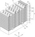
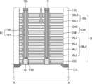
도 2를 참조하면, 본 발명의 실시예들에 따라 제조한 3차원 반도체 메모리 장치의 셀 어레이는, 공통 소오스 라인(CSL), 복수 개의 비트 라인(BL), 및 공통 소오스 라인(CSL)과 비트 라인(BL) 사이에 배치되는 복수 개의 셀 스트링(CSTR)을 포함할 수 있다.Referring to FIG. 2, a cell array of a three-dimensional semiconductor memory device manufactured according to embodiments of the present invention may include a common source line (CSL), a plurality of bit lines (BL), and a plurality of cell strings (CSTR) arranged between the common source line (CSL) and the bit lines (BL).
복수 개의 비트 라인(BL)은 2차원적으로 배치되고, 각각에는 복수 개의 셀 스트링(CSTR)이 병렬로 연결된다. 공통 소오스 라인(CSL)에는 복수 개의 셀 스트링(CSTR)이 공통으로 연결될 수 있다. 즉, 복수 개의 비트 라인과 하나의 공통 소오스 라인(CSL) 사이에 복수 개의 셀 스트링(CSTR)이 배치될 수 있다. 또한, 복수 개의 공통 소오스 라인(CSL)은 2차원적으로 배치될 수 있다. 여기에서, 복수 개의 공통 소오스 라인(CSL)에는 전기적으로 동일한 전압이 인가되거나, 복수 개의 공통 소오스 라인(CSL) 각각이 전기적으로 그리고 독립적으로 제어될 수도 있다.A plurality of bit lines (BL) are arranged two-dimensionally, and a plurality of cell strings (CSTR) are connected in parallel to each of them. A plurality of cell strings (CSTR) can be commonly connected to a common source line (CSL). That is, a plurality of cell strings (CSTR) can be arranged between a plurality of bit lines and one common source line (CSL). In addition, the plurality of common source lines (CSL) can be arranged two-dimensionally. Here, the plurality of common source lines (CSL) may be electrically applied with the same voltage, or each of the plurality of common source lines (CSL) may be electrically and independently controlled.
복수 개의 셀 스트링(CSTR) 각각은, 공통 소오스 라인(CSL)에 접속하는 접지 선택 트랜지스터(GST), 비트 라인(BL)에 접속하는 스트링 선택 트랜지스터(SST), 및 접지 선택 트랜지스터와 스트링 선택 트랜지스터(GST, SST) 사이에 배치되는 복수 개의 메모리 셀 트랜지스터들(MCT)로 구성될 수 있다. 또한, 접지 선택 트랜지스터(GST), 스트링 선택 트랜지스터(SST), 및 메모리 셀 트랜지스터(MCT)들은 직렬로 연결될 수 있다.Each of the plurality of cell strings (CSTR) may be composed of a ground select transistor (GST) connected to a common source line (CSL), a string select transistor (SST) connected to a bit line (BL), and a plurality of memory cell transistors (MCT) disposed between the ground select transistor and the string select transistor (GST, SST). Additionally, the ground select transistor (GST), the string select transistor (SST), and the memory cell transistors (MCT) may be connected in series.
공통 소오스 라인(CSL)은 접지 선택 트랜지스터(GST)들의 소오스들에 공통으로 연결될 수 있다. 이에 더하여, 공통 소오스 라인(CSL)과 비트 라인(BL) 사이에 배치되는, 접지 선택 라인(GSL), 복수 개의 워드라인(WL0-WL3), 및 복수 개의 스트링 선택 라인(SSL)이 접지 선택 트랜지스터(GST), 메모리 셀 트랜지스터(MCT) 및 스트링 선택 트랜지스터(SST)의 게이트 전극들로서 각각 사용될 수 있다. 또한, 메모리 셀 트랜지스터(MCT)들 각각은 데이터 저장 소자(data storage elements)를 포함한다.A common source line (CSL) may be commonly connected to sources of ground select transistors (GSTs). In addition, a ground select line (GSL), a plurality of word lines (WL0-WL3), and a plurality of string select lines (SSL), which are arranged between the common source line (CSL) and the bit line (BL), may be used as gate electrodes of the ground select transistor (GST), the memory cell transistor (MCT), and the string select transistor (SST), respectively. In addition, each of the memory cell transistors (MCTs) includes data storage elements.
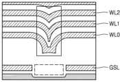
도 3을 참조하면, 기판(110)이 제공된다. 기판(110)은 제1 도전형, 예를 들면 P형을 가질 수 있다. 기판(110) 상에 버퍼 유전막(122)이 제공될 수 있다. 버퍼 유전막(122)은 MTO(middle temperature oxide)와 같은 실리콘 산화막일 수 있다. 버퍼 유전막(122) 상에, 절연 패턴들(125) 및 절연 패턴들을 개재하여 서로 이격된 수평 전극들이 제공될 수 있다.Referring to FIG. 3, a substrate (110) is provided. The substrate (110) may have a first conductive type, for example, a P type. A buffer dielectric film (122) may be provided on the substrate (110). The buffer dielectric film (122) may be a silicon oxide film, such as a middle temperature oxide (MTO). On the buffer dielectric film (122), insulating patterns (125) and horizontal electrodes spaced apart from each other by interposing the insulating patterns may be provided.
상기 수평 전극들은 접지 선택 라인(GSL), 제1 내지 제4 워드 라인들(WL0 내지 WL3), 및 스트링 선택 라인(SSL)을 포함할 수 있다. 절연 패턴들(125)은 실리콘 산화막일 수 있다. 버퍼 유전막(122)은 절연 패턴들(125)에 비하여 얇을 수 있다. 수평 전극들은 도핑된 실리콘, 금속(예를 들어, 텅스텐), 금속 질화물(예를 들어, 티타늄 질화물), 금속 실리사이드 또는 이들의 조합을 포함할 수 있다. 수평 전극들은, 예를 들어 배리어막, 및 배리어막 상의 금속막을 포함할 수 있다. 배리어막은 금속 질화물, 예를 들어 티타늄 질화물일 수 있다. 금속막은, 예를 들어 텅스텐일 수 있다.The horizontal electrodes may include a ground select line (GSL), first to fourth word lines (WL0 to WL3), and a string select line (SSL). The insulating patterns (125) may be a silicon oxide film. The buffer dielectric film (122) may be thinner than the insulating patterns (125). The horizontal electrodes may include doped silicon, a metal (e.g., tungsten), a metal nitride (e.g., titanium nitride), a metal silicide, or a combination thereof. The horizontal electrodes may include, for example, a barrier film, and a metal film on the barrier film. The barrier film may be a metal nitride, for example, titanium nitride. The metal film may be, for example, tungsten.
절연 패턴들(125) 및 수평 전극들은 게이트 구조체(G)를 구성할 수 있다. 게이트 구조체(G)는 제1 방향(D1)을 따라 수평적으로 연장할 수 있다. 복수개의 게이트 구조체들(G)이 기판(110) 상에 제공될 수 있다. 게이트 구조체들(G)은 제1 방향과 교차하는 제2 방향(D2)으로 서로 마주볼 수 있다. 스트링 선택 라인들(SSL)은 제2 방향(D2)으로 서로 분리되고, 제1 방향(D1)으로 연장될 수 있다. 도면에는, 하나의 게이트 구조체(G)에서, 스트링 선택 라인(SSL1, SSL2)이 복수 개이고 접지 선택 라인(GSL)이 1개인 것을 도시하나, 이에 한정되지 않는다.Insulating patterns (125) and horizontal electrodes may form a gate structure (G). The gate structure (G) may extend horizontally along a first direction (D1). A plurality of gate structures (G) may be provided on a substrate (110). The gate structures (G) may face each other in a second direction (D2) intersecting the first direction. The string selection lines (SSL) may be separated from each other in the second direction (D2) and may extend in the first direction (D1). In the drawing, in one gate structure (G), there are a plurality of string selection lines (SSL1, SSL2) and one ground selection line (GSL), but the present invention is not limited thereto.
게이트 구조체들(G) 사이에, 제1 방향(D1)으로 신장하는 분리 영역(121)이 제공될 수 있다. 공통 소오스 라인들(CSL)이 분리 영역(121)의 기판(110)에 제공된다. 공통 소오스 라인들(CSL)은, 서로 이격되어, 기판(110) 내에서 제1 방향(D1)으로 연장할 수 있다. 공통 소오스 라인들(CSL)은, 제1 도전형과 다른 제2 도전형(예를 들면, N형)을 가질 수 있다. 도면에 도시된 것과는 달리, 공통 소오스 라인들(CSL)은 인접하는 두 접지 선택라인(GSL)의 사이에서 기판(110) 내에 제공되고 제1 방향(D1)으로 연장하는 라인 형상의 패턴일 수 있다.Between the gate structures (G), a separation region (121) extending in a first direction (D1) may be provided. Common source lines (CSL) are provided on the substrate (110) of the separation region (121). The common source lines (CSL) may be spaced apart from each other and may extend in the first direction (D1) within the substrate (110). The common source lines (CSL) may have a second conductivity type (e.g., N type) different from the first conductivity type. Unlike what is illustrated in the drawing, the common source lines (CSL) may be a line-shaped pattern provided within the substrate (110) between two adjacent ground selection lines (GSL) and extending in the first direction (D1).
복수 개의 셀 기둥들(PL)이, 수평 전극들(GSL, WL0 내지 WL3, SSL)을 관통하여 기판(110)에 연결된다. 셀 기둥들(PL)은 기판(110)으로부터 수직 방향으로 위로 연장되는(즉, 제3 방향(D3)으로 연장되는) 장축을 가질 수 있다. 셀 기둥들(PL)의 일단들은 기판(110)에 연결되고, 이들의 타단들은 제2 방향(D2)으로 연장하는 배선들에 연결될 수 있다. 상기 배선들은 서로 인접하며 제2 방향(D2)으로 연장하는 제1 배선(BL1) 및 제2 배선(BL2)을 포함할 수 있다.A plurality of cell columns (PL) are connected to a substrate (110) through horizontal electrodes (GSL, WL0 to WL3, SSL). The cell columns (PL) may have a longitudinal axis extending vertically upward from the substrate (110) (i.e., extending in a third direction (D3)). One ends of the cell columns (PL) may be connected to the substrate (110), and the other ends thereof may be connected to wirings extending in a second direction (D2). The wirings may include a first wiring (BL1) and a second wiring (BL2) that are adjacent to each other and extend in the second direction (D2).
하나의 스트링 선택라인(SSL)에 결합된 복수 개의 셀 기둥들(PL)은 지그 재그(zig-zag) 또는 스태거형(staggered)으로 배치될 수 있다. 복수 개의 셀 기둥들(PL)은 동일한 하나의 스트링 선택라인(SSL)에 결합된 제1 셀 기둥들(PL1) 및 제2 셀 기둥들(PL2)을 포함할 수 있다. 제1 셀 기둥들(PL1)은 분리 영역(121)에 가장 인접하고, 제2 셀 기둥들(PL2)은 분리 영역(121)에서 보다 떨어져 있다. 제2 셀 기둥들(PL2)은 제1 셀 기둥들(PL1)로부터 제1 방향(D1) 및 제2 방향(D2)으로 시프트된다. 제1 셀 기둥들(PL1) 및 제2 셀 기둥들(PL2)은, 도전 패턴(136) 및 콘택(138)을 통하여, 제1 상부 배선(BL1) 및 제2 상부 배선(BL2)에 각각 연결될 수 있다.A plurality of cell columns (PL) coupled to a single string selection line (SSL) may be arranged in a zig-zag or staggered manner. The plurality of cell columns (PL) may include first cell columns (PL1) and second cell columns (PL2) coupled to the same single string selection line (SSL). The first cell columns (PL1) are closest to the separation region (121), and the second cell columns (PL2) are further away from the separation region (121). The second cell columns (PL2) are shifted from the first cell columns (PL1) in the first direction (D1) and the second direction (D2). The first cell columns (PL1) and the second cell columns (PL2) may be connected to the first upper wiring (BL1) and the second upper wiring (BL2), respectively, through the conductive pattern (136) and the contact (138).
배선들(BL1, BL2)과 공통 소오스 라인들(CSL) 사이에 복수 개의 셀 스트링들이 제공된다. 배선들(BL1, BL2)은 플래시 메모리 장치의 비트 라인들일 수 있다. 하나의 셀 스트링은, 배선들(BL1, BL2)에 접속하는 스트링 선택 트랜지스터, 공통 소오스 라인들(CSL)에 접속하는 접지 선택 트랜지스터, 및 스트링 선택 트랜지스터와 접지 선택 트랜지스터 사이에 제공되는 복수개의 수직 스트링 메모리 셀들을 포함할 수 있다. 접지 선택 라인(GSL)은 접지 선택 트랜지스터의 접지 선택 게이트, 워드 라인들(WL0 내지 WL3)은 복수개의 수직형 메모리 셀들의 셀 게이트들, 스트링 선택 라인(SSL)은 스트링 선택 트랜지스터의 스트링 선택 게이트에 대응될 수 있다. 복수개의 메모리 셀들(MC)이 하나의 셀 기둥(PL)에 제공된다. 접지 선택 게이트는 플래시 메모리 장치의 접지 선택 게이트일 수 있다. 스트링 선택 게이트는 플래시 메모리 장치의 스트링 선택 게이트일 수 있다.A plurality of cell strings are provided between wires (BL1, BL2) and common source lines (CSL). The wires (BL1, BL2) may be bit lines of a flash memory device. One cell string may include a string select transistor connected to the wires (BL1, BL2), a ground select transistor connected to the common source lines (CSL), and a plurality of vertical string memory cells provided between the string select transistor and the ground select transistor. The ground select line (GSL) may correspond to a ground select gate of the ground select transistor, the word lines (WL0 to WL3) may correspond to cell gates of the plurality of vertical memory cells, and the string select line (SSL) may correspond to a string select gate of the string select transistor. A plurality of memory cells (MC) are provided in one cell column (PL). The ground select gate may be a ground select gate of a flash memory device. The string select gate may be a string select gate of a flash memory device.
워드 라인들(WL0 내지 WL3)과 셀 기둥들(PL) 사이에, 정보저장 요소(130)가 제공될 수 있다. 상기 정보저장 요소(130)는 전하 저장막일 수 있다. 예를 들면, 정보저장 요소(130)는 트랩 절연막, 부유 게이트 전극, 또는 도전성 나노 도트들(conductive nano dots)을 포함하는 절연막 중의 어느 하나일 수 있다. 도 3에는, 정보저장 요소(130)가 절연 패턴들(125)과 워드 라인들(WL0 내지 WL3) 사이로 연장하는 것이 도시되어 있다. 도시와는 달리, 정보저장 요소(130)의 적어도 일부는 절연 패턴들(125)과 셀 기둥들(PL) 사이로 연장할 수 있다. 스트링 및 접지 선택 라인들(SSL, GSL)과 셀 기둥들(PL) 사이에는, 정보저장 요소(130) 대신 게이트 절연막이 제공될 수 있다.Between the word lines (WL0 to WL3) and the cell pillars (PL), an information storage element (130) may be provided. The information storage element (130) may be a charge storage film. For example, the information storage element (130) may be any one of a trap insulating film, a floating gate electrode, or an insulating film including conductive nano dots. In FIG. 3, the information storage element (130) is illustrated as extending between the insulating patterns (125) and the word lines (WL0 to WL3). Contrary to the illustration, at least a portion of the information storage element (130) may extend between the insulating patterns (125) and the cell pillars (PL). Instead of the information storage element (130), a gate insulating film may be provided between the string and ground selection lines (SSL, GSL) and the cell pillars (PL).
접지 선택 라인들(GSL)과 셀 기둥들(PL)들 사이, 또는 스트링 선택 라인들(SSL1, SSL2)과 셀 기둥들(PL)들 사이에는, 트랜지스터의 게이트 절연막으로 사용되는 유전막이 배치될 수 있다. 여기서, 유전막은 정보저장 요소(130)와 동일한 물질로 형성될 수도 있으며, 통상적인 MOSFET을 위한 게이트 절연막(예를 들면, 실리콘 산화막)일 수도 있다.Between the ground selection lines (GSL) and the cell columns (PL), or between the string selection lines (SSL1, SSL2) and the cell columns (PL), a dielectric film used as a gate insulating film of the transistor may be arranged. Here, the dielectric film may be formed of the same material as the information storage element (130), and may be a gate insulating film (for example, a silicon oxide film) for a typical MOSFET.
이러한 구조에서, 셀 기둥들(PL)은, 접지 선택 라인들(GSL), 워드 라인들(WL0 내지 WL3) 및 스트링 선택 라인들(SSL1, SSL2)과 함께, 셀 기둥들(PL)을 채널 영역으로 사용하는 모스펫(MOSFET)을 구성할 수 있다. 이와 달리, 셀 기둥들(PL)은, 접지 선택 라인들(GSL), 워드 라인들(WL0 내지 WL3) 및 스트링 선택 라인들(SSL1, SSL2)과 함께, 모스 커패시터(MOS capacitor)를 구성할 수도 있다.In this structure, the cell columns (PL) can form a MOSFET that uses the cell columns (PL) as a channel region together with the ground select lines (GSL), the word lines (WL0 to WL3), and the string select lines (SSL1, SSL2). Alternatively, the cell columns (PL) can form a MOS capacitor together with the ground select lines (GSL), the word lines (WL0 to WL3), and the string select lines (SSL1, SSL2).
접지 선택 라인들(GSL), 워드 라인들(WL0 내지 WL3) 및 스트링 선택 라인들(SSL1, SSL2)은 선택 트랜지스터 및 셀 트랜지스터의 게이트 전극들로서 각각 사용될 수 있다. 또한, 접지 선택 라인들(GSL), 워드 라인들(WL0 내지 WL3) 및 스트링 선택 라인들(SSL1, SSL2)에 인가되는 전압으로부터의 기생 전계(fringe field)에 의해 셀 기둥들(PL)에 반전 영역들(inversion regions)이 형성될 수 있다. 여기에서, 반전 영역의 최대 거리(또는 폭)는 반전 영역을 생성시키는 워드 라인들 또는 선택 라인들의 두께보다 클 수 있다. 이에 따라, 셀 기둥들(PL)에 형성되는 반전 영역들은 수직적으로 중첩되어, 공통 소오스 라인(CSL)으로부터 선택된 비트 라인을 전기적으로 연결하는 전류 통로를 형성할 수 있다. 즉, 셀 스트링(CSTR)은, 접지 및 스트링 선택 라인들(GSL, SSL1, SSL2)에 의해 구성되는 접지 및 스트링 트랜지스터들과, 워드 라인들(WL0 내지 WL3)에 의해 구성되는 메모리 셀 트랜지스터들(도 2의 MCT)이 직렬 연결된 구조를 가질 수 있다.The ground select lines (GSL), the word lines (WL0 to WL3), and the string select lines (SSL1, SSL2) can be used as gate electrodes of the select transistor and the cell transistor, respectively. In addition, inversion regions can be formed in the cell pillars (PL) by a fringe field from a voltage applied to the ground select lines (GSL), the word lines (WL0 to WL3), and the string select lines (SSL1, SSL2). Here, the maximum distance (or width) of the inversion region can be greater than the thickness of the word lines or the select lines that generate the inversion region. Accordingly, the inversion regions formed in the cell pillars (PL) can vertically overlap to form a current path that electrically connects a selected bit line from a common source line (CSL). That is, the cell string (CSTR) may have a structure in which ground and string transistors configured by ground and string select lines (GSL, SSL1, SSL2) and memory cell transistors (MCT of FIG. 2) configured by word lines (WL0 to WL3) are connected in series.
일부 실시예들에 있어서, 상기 스트링 선택 라인들(SSL1, SSL2)과 워드 라인들(WL0 내지 WL3)의 사이에는 더미 워드 라인들(DM1, DM2)이 배치될 수 있다. 상기 더미 워드 라인들(DM1, DM2)은, 상기 스트링 선택 라인들(SSL1, SSL2)에서의 문턱 전압의 산포를 균일하게 유지하여 셀 전류 감소를 방지하는 역할을 수행할 수 있다.In some embodiments, dummy word lines (DM1, DM2) may be arranged between the string selection lines (SSL1, SSL2) and the word lines (WL0 to WL3). The dummy word lines (DM1, DM2) may serve to prevent cell current reduction by uniformly maintaining the threshold voltage distribution in the string selection lines (SSL1, SSL2).
도 4a는 본 발명의 일 실시예에 따른 수직형 반도체 메모리 장치의 한 쪽 단부를 개념적으로 나타낸 부분 사시도이고, 도 4b는 이를 제 2 방향(D2)에서 바라본 측단면도이다. 도 5는 상기 수직형 반도체 메모리 장치의 한 쪽 단부를 개념적으로 나타낸 평면도이다.FIG. 4a is a partial perspective view conceptually illustrating one end of a vertical semiconductor memory device according to one embodiment of the present invention, and FIG. 4b is a side cross-sectional view thereof viewed in a second direction (D2). FIG. 5 is a plan view conceptually illustrating one end of the vertical semiconductor memory device.
도 4a, 도 4b 및 도 5를 참조하면, 셀 어레이 영역(A)과 연결 영역(B)이 인접하여 배치된다. 메모리 셀들과 주변 회로들을 연결하는 컨택 플러그들 및 배선들이 형성되는 연결 영역(B)이 셀 어레이 영역(A)에 인접하여 배치됨은 도 1을 참조하여 설명한 바와 같다.Referring to FIGS. 4A, 4B, and 5, the cell array region (A) and the connection region (B) are arranged adjacently. As described with reference to FIG. 1, the connection region (B), where contact plugs and wires connecting memory cells and peripheral circuits are formed, is arranged adjacent to the cell array region (A).
연결 영역(B)에서 상기 게이트 구조체(G)들은 주변 회로 영역과의 전기적인 연결을 위해 계단식 구조(stepwise structure)를 가질 수 있다. 상기 계단식 구조는 게이트 구조체(G)들이 제 1 방향으로 연장되면서 스트링 선택 라인들(SSL2, SSL1), 더미 워드 라인들(DM2, DM1), 워드 라인들(WL3 내지 WL0), 및 접지 선택 라인(GSL)의 순서로 점점 길어지면서 각각의 말단부가 인접하는 상부의 수평 전극으로부터 돌출될 수 있다.In the connection region (B), the gate structures (G) may have a stepwise structure for electrical connection with a peripheral circuit region. In the stepwise structure, the gate structures (G) may extend in the first direction and gradually become longer in the order of string selection lines (SSL2, SSL1), dummy word lines (DM2, DM1), word lines (WL3 to WL0), and ground selection lines (GSL), and each end may protrude from an adjacent upper horizontal electrode.
상기 반도체 메모리 장치는 적어도 제 1 워드 라인 스택과 제 2 워드 라인 스택을 포함할 수 있다. 제 1 워드 라인 스택은 셀 어레이 영역(A)에서 적층된 제 1 워드 라인들(WLA)을 포함할 수 있다. 제 2 워드 라인 스택은 셀 어레이 영역(A)에서 적층된 제 2 워드 라인들(WLB)을 포함할 수 있다. 위에서 설명한 바와 같이 제 1 워드 라인들(WLA)과 제 2 워드 라인들(WLB)은 각각 연결 영역(B)까지 연장될 수 있으며 이들의 단부는 계단식 구조를 가질 수 있다. 일부 실시예들에 있어서, 제 1 워드 라인들(WLA)과 제 2 워드 라인들(WLB)의 단부는 상기 연결 영역(B)에서 수직 방향인 제3 방향(D3)으로 꺾여서 연장될 수 있다.The semiconductor memory device may include at least a first word line stack and a second word line stack. The first word line stack may include first word lines (WLA) stacked in a cell array region (A). The second word line stack may include second word lines (WLB) stacked in the cell array region (A). As described above, the first word lines (WLA) and the second word lines (WLB) may each extend to a connection region (B), and ends thereof may have a step-like structure. In some embodiments, ends of the first word lines (WLA) and the second word lines (WLB) may extend in a third direction (D3) that is vertical to the connection region (B).
상기 반도체 메모리 장치는 제 1 워드 라인 스택과 제 2 워드 라인 스택에 인접하여 제 3 워드 라인 스택 및 제 4 워드 라인 스택을 더 포함할 수 있다. 상기 제 3 워드 라인 스택 및 제 4 워드 라인 스택의 구성은 상기 제 1 워드 라인 스택 및 제 2 워드 라인 스택의 구성과 실질적으로 동일하므로 여기서는 중복되는 설명을 생략한다.The semiconductor memory device may further include a third word line stack and a fourth word line stack adjacent to the first word line stack and the second word line stack. The configurations of the third word line stack and the fourth word line stack are substantially the same as the configurations of the first word line stack and the second word line stack, so that a redundant description is omitted herein.
상기 제 1 워드 라인 스택 내지 제 4 워드 라인 스택은 하나의 메모리 블록(memory block)을 구성할 수 있다. 일부 실시예들에 있어서, 상기 제 1 워드 라인 스택 및 제 2 워드 라인 스택은 하나의 메모리 블록을 구성할 수 있다.The first to fourth word line stacks may form one memory block. In some embodiments, the first word line stack and the second word line stack may form one memory block.
상기 제 1 워드 라인 스택의 스트링 선택 라인(SSL)과 상기 제 2 워드 라인 스택의 스트링 선택 라인(SSL)은 물리적으로 및 전기적으로 분리되어 있다.The string select line (SSL) of the first word line stack and the string select line (SSL) of the second word line stack are physically and electrically separated.
셀 어레이 영역(A)에서는 상기 제 1 워드 라인 스택 내지 제 4 워드 라인 스택이 분리 영역(121)에 의하여 상호 분리되어 있다. 하지만, 일부 실시예들에 있어서, 제 1 워드 라인 스택과 제 2 워드 라인 스택은 연결 영역(B)에서 적어도 부분적으로 연결될 수 있다. 예를 들면, 제 1 워드 라인 스택의 워드 라인들(W0 내지 W3) 및 더미 워드 라인들(DM)은 제 2 워드 라인 스택의 워드 라인들(W0 내지 W3) 및 더미 워드 라인들(DM)과 연결될 수 있다.In the cell array region (A), the first word line stack to the fourth word line stack are separated from each other by the separation region (121). However, in some embodiments, the first word line stack and the second word line stack may be at least partially connected in the connection region (B). For example, the word lines (W0 to W3) and dummy word lines (DM) of the first word line stack may be connected to the word lines (W0 to W3) and dummy word lines (DM) of the second word line stack.
일부 실시예들에 있어서, 제 1 워드 라인 스택 내지 제 4 워드 라인 스택은 연결 영역(B)에서 적어도 부분적으로 연결될 수 있다. 예를 들면, 제 1 워드 라인 스택 내지 제 4 워드 라인 스택의 워드 라인들(W0 내지 W3) 및 더미 워드 라인들(DM)은 서로서로 연결될 수 있다.In some embodiments, the first word line stack to the fourth word line stack may be at least partially connected in the connection region (B). For example, the word lines (W0 to W3) and the dummy word lines (DM) of the first word line stack to the fourth word line stack may be connected to each other.
제 1 워드 라인 스택 내지 제 4 워드 라인 스택은 브릿지(BG)에 의하여 연결될 수 있다. 보다 구체적으로 제 1 워드 라인 스택의 워드 라인들(W0 내지 W3)은 제2 내지 제 4 워드 라인 스택의 대응되는 워드 라인들(W0 내지 W3)과 브릿지(BG)에 의하여 연결될 수 있다. 또, 제 1 워드 라인 스택의 더미 워드 라인들(DM)은 제2 내지 제 4 워드 라인 스택의 대응되는 더미 워드 라인들(DM)과 브릿지(BG)에 의하여 연결될 수 있다. 도 4a, 도 4b 및 도 5에서는 브릿지(BG)를 보다 명확하게 표현하기 위하여 더미 워드 라인(DM2)의 제1 방향으로 돌출된 폭이 다소 과장되게 도시되었으며, 각 수평 전극들은 실질적으로 일정한 폭으로 제1 방향으로 돌출될 수 있다.The first to fourth word line stacks may be connected by bridges (BG). More specifically, the word lines (W0 to W3) of the first word line stack may be connected to the corresponding word lines (W0 to W3) of the second to fourth word line stacks by bridges (BG). In addition, the dummy word lines (DM) of the first word line stack may be connected to the corresponding dummy word lines (DM) of the second to fourth word line stacks by bridges (BG). In FIGS. 4A, 4B, and 5, the width of the dummy word line (DM2) protruding in the first direction is somewhat exaggerated in order to more clearly express the bridge (BG), and each of the horizontal electrodes may protrude in the first direction with a substantially constant width.
상기 제 1 워드 라인 스택의 접지 선택 라인(GSL)과 상기 제 2 워드 라인 스택의 접지 선택 라인(GSL)은 물리적으로 분리될 수 있다. 상기 제 1 워드 라인 스택의 접지 선택 라인(GSL)은 상기 제 2 워드 라인 스택의 접지 선택 라인(GSL)과 물리적으로 연결되거나 일체형으로 형성될 수도 있는데, 이들이 물리적으로 서로 분리되면 보다 신속한 동작과 같은 우수한 전기적 특성을 얻을 수 있다.The ground select line (GSL) of the first word line stack and the ground select line (GSL) of the second word line stack can be physically separated. The ground select line (GSL) of the first word line stack can be physically connected to the ground select line (GSL) of the second word line stack or can be formed integrally with it. If they are physically separated from each other, superior electrical characteristics such as faster operation can be obtained.
앞서 설명한 바와 같이, 상기 제 1 워드 라인 스택 내지 제 4 워드 라인 스택의 워드 라인들(W0 내지 W3)과 더미 워드 라인들(DM)은 브릿지(BG)에 의하여 서로 연결되어 있다. 따라서, 상기 제 1 워드 라인 스택 내지 제 4 워드 라인 스택의 워드 라인들(W0 내지 W3)과 더미 워드 라인들(DM) 중 어느 하나가 주변 회로 영역과 연결되기 위해서는 하나의 상부 배선으로 충분할 수 있다. 보다 구체적으로, 상기 제 1 워드 라인 스택 내지 제 4 워드 라인 스택의 워드 라인(WL3)을 주변 회로 영역과 연결하기 위하여 상부 배선(UL3)만 있으면 되고, 대응되는 동일한 레벨의 층에 대하여 워드 라인 스택마다 상부 배선이 존재할 필요가 없다. 이는 대응되는 동일한 레벨의 층에 있는 워드 라인들이 브릿지(BG)에 의하여 연결되어 있기 때문이다.As described above, the word lines (W0 to W3) of the first to fourth word line stacks and the dummy word lines (DM) are connected to each other by the bridge (BG). Therefore, one upper wiring may be sufficient for connecting either the word lines (W0 to W3) of the first to fourth word line stacks or the dummy word lines (DM) to a peripheral circuit area. More specifically, only the upper wiring (UL3) is required to connect the word line (WL3) of the first to fourth word line stacks to the peripheral circuit area, and there is no need for an upper wiring for each word line stack for the corresponding same-level layer. This is because the word lines in the corresponding same-level layer are connected by the bridge (BG).
이와 같은 브릿지(BG)는 상기 제 1 워드 라인 스택 내지 제 4 워드 라인 스택을 형성하기 위하여 분리 영역(121)을 형성하면서 일시에 형성될 수 있는데, 이와 같이 하는 경우 최하부에 배치되는 접지 선택 라인(GSL)도 브릿지(BG)에 의하여 서로 연결될 우려가 있다. 이를 방지하기 위하여 상기 브릿지(BG)에 대응되는 접지 선택 라인(GSL)의 부분을 미리 제거할 수 있다.Such a bridge (BG) may be formed simultaneously while forming a separation region (121) to form the first to fourth word line stacks. In this case, there is a risk that the ground selection line (GSL) positioned at the bottom may also be connected to each other by the bridge (BG). To prevent this, a portion of the ground selection line (GSL) corresponding to the bridge (BG) may be removed in advance.
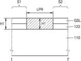
도 6은 본 발명의 일 실시예에 따른, 브릿지(BG)에 대응되는 접지 선택 라인(GSL)의 부분을 제거한 후의 모습을 나타낸 평면도이다.FIG. 6 is a plan view showing an appearance after removing a portion of a ground selection line (GSL) corresponding to a bridge (BG) according to one embodiment of the present invention.
도 6을 참조하면, 제 1 워드 라인 스택의 접지 선택 라인(GSL)과 제 2 워드 라인 스택의 접지 선택 라인(GSL)은 국부 평탄화 영역(LPR)에 의하여 서로 분리될 수 있다. 상기 국부 평탄화 영역(LPR)의 외연이 반드시 그의 상부에 배치되는 브릿지(BG)의 외연과 일치할 필요는 없다.Referring to FIG. 6, the ground select line (GSL) of the first word line stack and the ground select line (GSL) of the second word line stack can be separated from each other by a local planarization region (LPR). The outer edge of the local planarization region (LPR) does not necessarily need to coincide with the outer edge of the bridge (BG) arranged thereon.
상기 국부 평탄화 영역(LPR)을 형성함으로써 인접하는 두 워드 라인 스택들의 접지 선택 라인(GSL)을 분리하면, 국부 평탄화 영역(LPR)의 면적에 대하여 접지 선택 라인(GSL)과 그에 대응되는 버퍼 유전막(122)의 높이로 정의되는 빈 공간이 생성된다. 상기 빈 공간은 융기된 기판(110) 또는 절연층과 같은 필러(F)에 의하여 적어도 부분적으로 충전될 수 있다. 상기 절연층은 예를 들면 실리콘 산화물일 수 있다.By forming the above local planarization region (LPR) to separate the ground selection lines (GSLs) of two adjacent word line stacks, a void space defined by the height of the ground selection line (GSL) and the corresponding buffer dielectric film (122) is created with respect to the area of the local planarization region (LPR). The void space can be at least partially filled by a filler (F), such as a raised substrate (110) or an insulating layer. The insulating layer can be, for example, silicon oxide.
또한 상기 국부 평탄화 영역(LPR) 근처에서 상기 접지 선택 라인(GSL)의 측면은 측방향의 리세스(GV)를 가질 수 있다. 도 6에서 보는 바와 같이, 상기 접지 선택 라인(GSL)의 측면은 직선을 따라 연장되다가 국부 평탄화 영역(LPR)에서 리세스(GV)를 갖고, 상기 리세스(GV)가 적어도 부분적으로 필러(F)에 의하여 필링될 수 있다.Additionally, a side surface of the ground selection line (GSL) near the local flattening region (LPR) may have a lateral recess (GV). As shown in FIG. 6, the side surface of the ground selection line (GSL) may extend along a straight line and have a recess (GV) at the local flattening region (LPR), and the recess (GV) may be at least partially filled by a filler (F).
도 7a 내지 도 7c는 본 발명의 실시예들에 따른 도 6의 I-I' 부분의 측단면을 나타낸 도면들이다.FIGS. 7A to 7C are cross-sectional views illustrating portions I-I' of FIG. 6 according to embodiments of the present invention.
도 7a를 참조하면, 필러(F)가 상기 국부 평탄화 영역(LPR) 상의 공간을 적어도 부분적으로 충전할 수 있다. 필러(F)를 상기 공간 내에 충전하기 위하여 화학 기상 증착, 물리 기상 증착, 또는 원자층 증착과 같은 방법들이 이용될 수 있다. 필러(F)는 상기 공간의 전부를 필링할 필요는 없다. 예를 들면, 상기 필러(F)의 제 3 방향(D1)으로의 최고 두께는 상기 접지 선택 라인(GSL) 및 버퍼 유전막(122)의 두께의 합(H1)의 약 40% 내지 약 140%일 수 있다. 또는 상기 필러(F)의 제 3 방향(D1)으로의 최고 두께는 상기 접지 선택 라인(GSL) 및 버퍼 유전막(122)의 두께의 합(H1)의 약 70% 내지 약 120%일 수 있다.Referring to FIG. 7a, the filler (F) can at least partially fill the space on the localized planarization region (LPR). Methods such as chemical vapor deposition, physical vapor deposition, or atomic layer deposition can be used to fill the space with the filler (F). The filler (F) does not need to fill the entire space. For example, the maximum thickness of the filler (F) in the third direction (D1) can be about 40% to about 140% of the sum (H1) of the thicknesses of the ground selection line (GSL) and the buffer dielectric film (122). Alternatively, the maximum thickness of the filler (F) in the third direction (D1) can be about 70% to about 120% of the sum (H1) of the thicknesses of the ground selection line (GSL) and the buffer dielectric film (122).
일부 실시예들에 있어서, 상기 필러(F)의 상부 표면은 상기 접지 선택 라인(GSL)의 상부 표면과 실질적으로 동일한 평면 상에 위치할 수 있다. 이를 위하여 화학 기상 증착과 같은 방법으로 상기 공간 내부를 완전히 매립하면서 상기 접지 선택 라인(GSL)의 상부를 덮도록 필러(F)의 물질막을 형성한 후 에치백(etch back) 또는 화학적 기계적 연마(chemical mechanical polishing, CMP)와 같은 방법을 이용하여 평탄화할 수 있다.In some embodiments, the upper surface of the filler (F) may be positioned substantially on the same plane as the upper surface of the ground selection line (GSL). To this end, a material film of the filler (F) may be formed to completely fill the inside of the space by a method such as chemical vapor deposition and cover the upper portion of the ground selection line (GSL), and then planarized by a method such as etch back or chemical mechanical polishing (CMP).
뒤에서 도 10a 내지 도 10i를 참조하여 설명하는 바와 같이 상기 접지 선택 라인(GSL)은 그의 위치에 희생층을 먼저 형성하고, 이를 도전성 물질로 치환함으로써 형성되는 방식으로 만들어 질 수 있다. 이러한 경우에는 화학 기상 증착과 같은 방법으로 상기 공간 내부를 완전히 매립하면서 상기 희생층의 상부를 덮도록 필러(F)의 물질막을 형성한 후 평탄화할 수 있다.As described with reference to FIGS. 10a to 10i below, the ground selection line (GSL) may be formed by first forming a sacrificial layer at its location and then replacing it with a conductive material. In this case, a material film of a filler (F) may be formed to cover the upper portion of the sacrificial layer while completely filling the inside of the space by a method such as chemical vapor deposition, and then planarized.
상기 국부 평탄화 영역(LPR)의 한 쪽 단부는 제 1 워드 라인 스택(S1)과 접할 수 있고, 다른 쪽 단부는 제 2 워드 라인 스택(S2)과 접할 수 있다. 도 7a에서는 구체적으로 도시하지 않았지만, 양 쪽 워드 라인 스택들(S1, S2)에서 상기 접지 선택 라인(GSL)의 상부에는 워드 라인들(WL0 내지 WL3)과 더미 워드 라인들(DM1, DM2)이 더 적층되고, 또한 서로 대응되는 워드 라인들(WL0 내지 WL3)과 더미 워드 라인들(DM1, DM2)이 상기 국부 평탄화 영역(LPR)의 상부에서 서로 연결될 수 있다.One end of the above-described local planarization region (LPR) can be in contact with the first word line stack (S1), and the other end can be in contact with the second word line stack (S2). Although not specifically illustrated in FIG. 7a, word lines (WL0 to WL3) and dummy word lines (DM1, DM2) are further stacked on the upper portion of the ground selection line (GSL) in both word line stacks (S1, S2), and further, corresponding word lines (WL0 to WL3) and dummy word lines (DM1, DM2) can be connected to each other on the upper portion of the above-described local planarization region (LPR).
도 7b는 본 발명의 다른 실시예에 따른 필러(F)를 나타낸 측단면도이다.FIG. 7b is a cross-sectional side view showing a filler (F) according to another embodiment of the present invention.
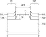
도 7b를 참조하면, 접지 선택 라인(GSL)과 그에 대응되는 버퍼 유전막(122)의 높이로 정의되는 빈 공간을 기판(110)이 융기되어 적어도 부분적으로 필링할 수 있다. 상기 필러(F)는 기판(110)이 자신의 상부 표면에 대하여 수직인 방향, 즉 제 3 방향(D3)으로 돌출된 형태를 가질 수 있다. 상기 돌출된 부분은 메사(mesa) 형태를 가질 수 있다. 일부 실시예들에 있어서, 상기 돌출된 부분의 측면은 경사면을 가질 수 있다.Referring to FIG. 7b, a substrate (110) may be raised to at least partially fill an empty space defined by a height of a ground selection line (GSL) and a corresponding buffer dielectric film (122). The filler (F) may have a shape in which the substrate (110) protrudes in a direction perpendicular to its upper surface, that is, in a third direction (D3). The protruding portion may have a mesa shape. In some embodiments, a side surface of the protruding portion may have an inclined surface.
상기 기판(110)의 융기된 부분의 상부 표면은 상기 제 1 워드 라인 스택(S1) 및/또는 상기 제 2 워드 라인 스택(S2)의 하부의 기판(110)의 표면에 비하여 융기되어 있을 수 있다.The upper surface of the raised portion of the substrate (110) may be raised compared to the surface of the substrate (110) below the first word line stack (S1) and/or the second word line stack (S2).
상기 기판(110)의 융기된 높이(H2)는 상기 접지 선택 라인(GSL) 및 버퍼 유전막(122)의 두께의 합(H1)의 약 40% 내지 약 140%일 수 있다. 또는 상기 기판(110)의 융기된 높이(H2)는 상기 접지 선택 라인(GSL) 및 버퍼 유전막(122)의 두께의 합(H1)의 약 70% 내지 약 120%일 수 있다. 예를 들면, 상기 기판(110)의 융기된 높이(H2)는 약 20Å 내지 약 300Å일 수 있다. 일부 실시예들에 있어서, 상기 기판(110)의 융기된 높이(H2)는 약 50Å 내지 약 200Å일 수 있다.The raised height (H2) of the substrate (110) may be about 40% to about 140% of the sum (H1) of the thicknesses of the ground selection line (GSL) and the buffer dielectric film (122). Alternatively, the raised height (H2) of the substrate (110) may be about 70% to about 120% of the sum (H1) of the thicknesses of the ground selection line (GSL) and the buffer dielectric film (122). For example, the raised height (H2) of the substrate (110) may be about 20 Å to about 300 Å. In some embodiments, the raised height (H2) of the substrate (110) may be about 50 Å to about 200 Å.
도 7b에서 보는 바와 같이, 상기 접지 선택 라인(GSL) 및 버퍼 유전막(122)은 제 2 워드 라인 스택(S2)에서와 같이 상기 국부 평탄화 영역(LPR)에 인접한 부분에서 평탄한 표면을 가질 수 있다. 일부 실시예들에 있어서, 상기 접지 선택 라인(GSL) 및 버퍼 유전막(122)은 제 1 워드 라인 스택(S2)에서와 같이 상기 국부 평탄화 영역(LPR)에 가까워질수록 상승하는 표면들을 가질 수 있다.As shown in FIG. 7b, the ground selection line (GSL) and the buffer dielectric film (122) may have flat surfaces adjacent to the local planarization region (LPR), as in the second word line stack (S2). In some embodiments, the ground selection line (GSL) and the buffer dielectric film (122) may have surfaces that rise as they get closer to the local planarization region (LPR), as in the first word line stack (S2).
도 7b에서 상기 버퍼 유전막(122)이 일부 제거되어 상기 기판(110)의 돌출부가 상기 버퍼 유전막(122)으로부터 노출되는 것으로 도시되었지만, 다른 실시예에서 상기 버퍼 유전막(122)이 상기 돌출부의 상부 표면을 전부 또는 부분적으로 덮고 있을 수도 있다.Although the buffer dielectric film (122) is partially removed in FIG. 7b to expose the protrusion of the substrate (110) from the buffer dielectric film (122), in other embodiments, the buffer dielectric film (122) may completely or partially cover the upper surface of the protrusion.
도 7c는 본 발명의 다른 실시예에 따른 필러(F)를 나타낸 측단면도이다.FIG. 7c is a cross-sectional side view showing a filler (F) according to another embodiment of the present invention.
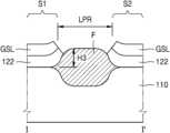
도 7c를 참조하면, 상기 국부 평탄화 영역(LPR) 내의 상기 필러(F)가 가장자리로 갈수록 점차 얇아지는 형태를 가질 수 있다. 특히, 상기 필러(F)의 측단면은 버즈 비크(bird's beak) 단면 형태를 갖는 가장자리를 가질 수 있다. 이와 같은 버즈 비크 단면은 기판(110)을 열산화시킴으로써 얻어진 것일 수 있다.Referring to FIG. 7c, the filler (F) within the local flattening region (LPR) may have a shape that gradually becomes thinner toward the edge. In particular, the side cross-section of the filler (F) may have an edge having a bird's beak cross-section shape. Such a bird's beak cross-section may be obtained by thermally oxidizing the substrate (110).
상기 필러(F)의 제 3 방향(D1)으로의 최고 두께에서, 상기 기판(110)의 평탄한 상부 표면과 상기 필러(F)의 상부 표면의 높이 차이(H3)는 상기 접지 선택 라인(GSL) 및 버퍼 유전막(122)의 두께의 합의 약 40% 내지 약 140%일 수 있다. 또는 상기 높이 차이(H3)는 상기 접지 선택 라인(GSL) 및 버퍼 유전막(122)의 두께의 합의 약 70% 내지 약 120%일 수 있다.At the highest thickness in the third direction (D1) of the filler (F), the height difference (H3) between the flat upper surface of the substrate (110) and the upper surface of the filler (F) may be about 40% to about 140% of the sum of the thicknesses of the ground selection line (GSL) and the buffer dielectric film (122). Alternatively, the height difference (H3) may be about 70% to about 120% of the sum of the thicknesses of the ground selection line (GSL) and the buffer dielectric film (122).
일부 실시예들에 있어서, 상기 기판(110)의 평탄한 상부 표면을 기준으로 상기 필러(F)의 상부 표면까지의 높이와 상기 필러(F)의 하부 표면까지의 깊이의 비는 약 50 : 50 내지 약 60 : 40일 수 있다. 일부 실시예들에 있어서, 상기 기판(110)의 평탄한 상부 표면을 기준으로 상기 필러(F)의 상부 표면까지의 높이와 상기 필러(F)의 하부 표면까지의 깊이의 비는 약 54 : 46일 수 있다.In some embodiments, a ratio of a height to an upper surface of the filler (F) based on a flat upper surface of the substrate (110) and a depth to a lower surface of the filler (F) may be about 50:50 to about 60:40. In some embodiments, a ratio of a height to an upper surface of the filler (F) based on a flat upper surface of the substrate (110) and a depth to a lower surface of the filler (F) may be about 54:46.
일부 실시예들에 있어서, 상기 접지 선택 라인(GSL) 및 버퍼 유전막(122)은 상기 국부 평탄화 영역(LPR)에 가까워질수록 상승하는 표면들을 가질 수 있다. 이와 같이 상승하는 표면은 버즈 비크(bird's beak)의 형상을 갖는 필러(F)에 기인하는 것일 수 있다.In some embodiments, the ground selection line (GSL) and the buffer dielectric film (122) may have surfaces that rise as they approach the local planarization region (LPR). Such rising surfaces may be due to a filler (F) having a bird's beak shape.
도 8은 이와 같은 필러(F)가 없이 접지 선택 라인(GSL) 및 워드 라인들(WL0, WL1, WL2)이 형성되었을 때의 브릿지의 단면을 나타낸 도면이다.Fig. 8 is a drawing showing a cross-section of a bridge when a ground selection line (GSL) and word lines (WL0, WL1, WL2) are formed without such a filler (F).
도 8을 참조하면, 접지 선택 라인(GSL)이 단절된 부분(점선 네모 부분)에서, 그 위에 적층된 워드 라인들(WL0, WL1, WL2) 및 이들을 절연하는 절연체들이 덴트(dent) 형상의 단면을 갖게 된다. 이와 같이 제조된 반도체 장치는 동작 시에 상기 덴트 부분(실선 네모 부분)에 전계가 집중되어 브레이크다운(breakdown)과 같은 불량이 발생할 수 있다.Referring to Fig. 8, in the part where the ground selection line (GSL) is disconnected (the dotted square part), the word lines (WL0, WL1, WL2) stacked thereon and the insulators that insulate them have a dent-shaped cross-section. In a semiconductor device manufactured in this way, when the electric field is concentrated in the dent part (the solid square part) during operation, a defect such as a breakdown may occur.
따라서, 도 7a 내지 도 7c와 같이 필러(F)로 상기 접지 선택 라인(GSL)이 단절된 부분(점선 네모 부분)을 적어도 부분적으로 필링하는 것이 필요하다.Therefore, it is necessary to at least partially fill the portion (dotted square portion) where the ground selection line (GSL) is disconnected with a filler (F) as shown in FIGS. 7a to 7c.
도 9는 본 발명의 다른 실시예에 따른, 브릿지(BG)에 대응되는 접지 선택 라인(GSL)의 부분을 제거한 후의 모습을 나타낸 평면도이다.FIG. 9 is a plan view showing the appearance after removing a portion of a ground selection line (GSL) corresponding to a bridge (BG) according to another embodiment of the present invention.
도 9를 참조하면, 제 1 워드 라인 스택의 접지 선택 라인(GSL)과 제 2 워드 라인 스택의 접지 선택 라인(GSL)의 사이에 국부 평탄화 영역(LPR)이 제공될 수 있다. 또, 제 1 워드 라인 스택의 접지 선택 라인(GSL)과 제 2 워드 라인 스택의 접지 선택 라인(GSL)은 각각 국부 평탄화 영역(LPR) 쪽을 향하여 측방향으로 연장되는 돌출부(GX)를 가질 수 있다. 도 9에서 보는 바와 같이, 상기 접지 선택 라인(GSL)의 측면은 직선을 따라 연장되다가 국부 평탄화 영역(LPR)에 인접하는 돌출부(GX)를 가질 수 있다.Referring to FIG. 9, a local planarization region (LPR) may be provided between a ground select line (GSL) of a first word line stack and a ground select line (GSL) of a second word line stack. In addition, the ground select line (GSL) of the first word line stack and the ground select line (GSL) of the second word line stack may each have a protrusion (GX) extending laterally toward the local planarization region (LPR). As shown in FIG. 9, a side surface of the ground select line (GSL) may have a protrusion (GX) extending along a straight line and adjacent to the local planarization region (LPR).
상기 제 1 워드 라인 스택의 접지 선택 라인(GSL)과 제 2 워드 라인 스택의 접지 선택 라인(GSL)은 국부 평탄화 영역(LPR)에 의하여 서로 분리될 수 있다. 상기 국부 평탄화 영역(LPR)의 외연이 반드시 그의 상부에 배치되는 브릿지(BG)의 외연과 일치할 필요는 없다.The ground select line (GSL) of the first word line stack and the ground select line (GSL) of the second word line stack can be separated from each other by a local planarization region (LPR). The outer edge of the local planarization region (LPR) does not necessarily need to coincide with the outer edge of the bridge (BG) arranged thereon.
도 10a 내지 도 10i는 본 발명의 일 실시예에 따른 반도체 메모리 장치의 제조 방법을 순서에 따라 나타낸 측단면도들이다. 도 10a 내지 도 10i에서 단면 A-A'는 도 6의 A-A' 선을 따른 절개면을 나타내고, 단면 B-B'는 도 6의 B-B' 선을 따른 절개면을 나타낸다.FIGS. 10A to 10I are cross-sectional side views sequentially illustrating a method for manufacturing a semiconductor memory device according to an embodiment of the present invention. In FIGS. 10A to 10I, cross-section A-A' represents a cut surface along line A-A' of FIG. 6, and cross-section B-B' represents a cut surface along line B-B' of FIG. 6.
도 10a를 참조하면, 기판(110)이 제공된다. 상기 기판(110)은 Si, Ge, 또는 SiGe를 포함할 수 있다. 다른 일부 실시예들에 있어서, 상기 기판(110)은 SOI (silicon-on-insulator) 기판, 또는 GeOI (germanium-on-insulator) 기판을 포함할 수 있다. 기판(110)은 제 1 도전형, 예를 들면 P형의 도전형을 가질 수 있다.Referring to FIG. 10A, a substrate (110) is provided. The substrate (110) may include Si, Ge, or SiGe. In some other embodiments, the substrate (110) may include a silicon-on-insulator (SOI) substrate, or a germanium-on-insulator (GeOI) substrate. The substrate (110) may have a first conductivity type, for example, a P-type conductivity type.
기판(110) 상에 버퍼 유전막(122)이 형성될 수 있다. 버퍼 유전막(122)은, 예를 들어 실리콘 산화막일 수 있다. 버퍼 유전막(122)은, 예를 들어 열산화 공정에 의하여 형성될 수 있다. 일부 실시예들에 있어서, 버퍼 유전막(122)은 MTO(middle temperature oxide)일 수 있다.A buffer dielectric film (122) may be formed on a substrate (110). The buffer dielectric film (122) may be, for example, a silicon oxide film. The buffer dielectric film (122) may be formed, for example, by a thermal oxidation process. In some embodiments, the buffer dielectric film (122) may be a middle temperature oxide (MTO).
상기 버퍼 유전막(122)의 위에는 추후 접지 선택 라인(GSL)을 형성하기 위한 희생막(123)이 제공될 수 있다. 상기 희생막(123)은 버퍼 유전막(122) 및 뒤에서 설명되는 절연막들(124, 도 10b 참조)에 대하여 습식 식각 특성이 다른 물질을 포함할 수 있다. 상기 희생막(123)은, 예를 들면 실리콘 질화막, 실리콘 산화질화막, 폴리실리콘막 또는 폴리실리콘게르마늄막을 포함할 수 있다. 상기 희생막(123)은 예를 들어, 화학 기상 증착(chemical vapor deposition, CVD) 방법에 의하여 형성될 수 있다.A sacrificial film (123) for forming a ground selection line (GSL) later may be provided on the buffer dielectric film (122). The sacrificial film (123) may include a material having different wet etching characteristics with respect to the buffer dielectric film (122) and the insulating films (124, see FIG. 10b) described later. The sacrificial film (123) may include, for example, a silicon nitride film, a silicon oxide nitride film, a polysilicon film, or a polysilicon germanium film. The sacrificial film (123) may be formed, for example, by a chemical vapor deposition (CVD) method.
이어서 국부 평탄화 영역(LPR)에 대하여 상기 버퍼 유전막(122) 및 상기 희생막(123)을 적어도 부분적으로 제거할 수 있다. 일부 실시예들에 있어서, 상기 국부 평탄화 영역(LPR)에서 상기 버퍼 유전막(122) 및 상기 희생막(123)의 전부가 제거될 수 있다. 선택적으로, 상기 국부 평탄화 영역(LPR)에서 상기 희생막(123)만 제거될 수 있다. 상기 버퍼 유전막(122) 및 상기 희생막(123)을 국부 평탄화 영역(LPR)에서 선택적으로 제거하기 위하여 포토 리소그래피 공정을 이용할 수 있다.Next, the buffer dielectric film (122) and the sacrificial film (123) can be at least partially removed in the local planarization region (LPR). In some embodiments, the entirety of the buffer dielectric film (122) and the sacrificial film (123) can be removed in the local planarization region (LPR). Optionally, only the sacrificial film (123) can be removed in the local planarization region (LPR). A photolithography process can be used to selectively remove the buffer dielectric film (122) and the sacrificial film (123) in the local planarization region (LPR).
상기 포토 리소그래피 공정에 의하여 상기 국부 평탄화 영역(LPR)에는 상기 버퍼 유전막(122) 및 상기 희생막(123)의 높이와 국부 평탄화 영역(LPR)의 면적에 의하여 정의되는 빈 공간이 형성될 수 있다.By the above photolithography process, a blank space defined by the height of the buffer dielectric film (122) and the sacrificial film (123) and the area of the local planarization region (LPR) can be formed in the local planarization region (LPR).
도 10b를 참조하면, 상기 버퍼 유전막(122) 및 상기 희생막(123)의 높이와 국부 평탄화 영역(LPR)의 면적에 의하여 정의되는 빈 공간을 산화물과 같은 필러(filler)를 적어도 부분적으로 필링(filling)한다. 상기 필러(F')는 융기된 기판(110) 또는 실리콘 산화물과 같은 절연층일 수 있다. 상기 필러(F')가 융기된 기판(110)인 실시예는 뒤에서 별도로 설명한다.Referring to FIG. 10b, a void space defined by the height of the buffer dielectric film (122) and the sacrificial film (123) and the area of the local planarization region (LPR) is at least partially filled with a filler such as oxide. The filler (F') may be a raised substrate (110) or an insulating layer such as silicon oxide. An embodiment in which the filler (F') is a raised substrate (110) will be described separately later.
상기 필러(F')가 실리콘 산화물인 경우, 퇴적 방법에 의하여 상기 공간이 필링될 수도 있고, 열산화 방법에 의하여 상기 공간이 필링될 수도 있다. 퇴적 방법은 예컨대 화학 기상 증착(CVD), 원자층 증착(atomic layer deposition, ALD), 또는 물리 기상 증착(physical vapor deposition, PVD)일 수 있으며 여기에 한정되는 것은 아니다.When the above filler (F') is silicon oxide, the space may be filled by a deposition method or by a thermal oxidation method. The deposition method may be, for example, chemical vapor deposition (CVD), atomic layer deposition (ALD), or physical vapor deposition (PVD), but is not limited thereto.
열산화 방법에 의해서는 버즈 비크(bird's beak) 단면 형태를 갖는 가장자리가 형성될 수 있으며, 이에 관해서는 앞서 도 7c를 참조하여 설명하였으므로 여기서는 상세한 설명을 생략한다.An edge having a bird's beak cross-section shape can be formed by the thermal oxidation method, and as this has been described above with reference to Fig. 7c, a detailed description thereof is omitted here.
이어서, 희생막들(123) 및 절연막들(124)이 버퍼 유전막(122) 상에 교대로 적층되어, 제공된다. 최상층의 절연막의 두께는 다른 절연막들의 두께보다 두꺼울 수 있다. 절연막들(124)은, 예를 들어 실리콘 산화막일 수 있다. 희생막들(123)은 버퍼 유전막(122) 및 절연막들(124)에 대하여 습식 식각 특성이 다른 물질을 포함할 수 있다. 희생막들(123)은, 예를 들면 실리콘 질화막, 실리콘 산화질화막, 폴리실리콘막 또는 폴리실리콘게르마늄막을 포함할 수 있다. 희생막들(123) 및 절연막들(124)은 예를 들어, 화학적 기상 증착(CVD) 방법에 의하여 형성될 수 있다.Next, sacrificial films (123) and insulating films (124) are alternately laminated on the buffer dielectric film (122) and provided. The thickness of the uppermost insulating film may be thicker than that of the other insulating films. The insulating films (124) may be, for example, a silicon oxide film. The sacrificial films (123) may include a material having different wet etching characteristics with respect to the buffer dielectric film (122) and the insulating films (124). The sacrificial films (123) may include, for example, a silicon nitride film, a silicon oxide nitride film, a polysilicon film, or a polysilicon germanium film. The sacrificial films (123) and the insulating films (124) may be formed by, for example, a chemical vapor deposition (CVD) method.
만일 상기 국부 평탄화 영역(LPR)을 필러(F')로 필링하지 않고 희생막들(123) 및 절연막들(124)을 적층한다면, 도 8에 나타낸 바와 같은 덴트(dent) 형상이 누적적으로 형성되기 때문에, 추후 형성될 수평 전극의, 국부 평탄화 영역(LPR)의 상부의 부분에서 전계가 집중되어 브레이크다운(breakdown)이 발생하는 등 제품 불량의 원인이 될 수 있다.If the sacrificial films (123) and the insulating films (124) are laminated without filling the above-mentioned localized flattening region (LPR) with filler (F'), a dent shape as shown in FIG. 8 is formed cumulatively, so that an electric field is concentrated in the upper part of the localized flattening region (LPR) of the horizontal electrode to be formed later, which may cause a breakdown or other product defect.
도 10c를 참조하면, 버퍼 유전막(122), 희생막들(123) 및 절연막들(124)을 관통하여, 기판(110)을 노출하는 셀 홀들(H)이 형성된다. 상기 셀 홀들(H)은 예컨대 포토 리소그래피 공정에 의하여 형성될 수 있다.Referring to FIG. 10c, cell holes (H) are formed to expose the substrate (110) by penetrating the buffer dielectric film (122), sacrificial films (123), and insulating films (124). The cell holes (H) may be formed, for example, by a photolithography process.
도 10d 및 도 10e를 참조하여, 셀 홀들(H) 내에 셀 기둥들(PL)이 형성되며, 셀 기둥들(PL)의 형성 공정을 보다 상세하게 설명하기 위하여 도 10d의 C 부분을 도 11에 나타내었고, 도 10e의 C 부분을 도 12에 나타내었다.Referring to FIGS. 10d and 10e, cell pillars (PL) are formed within cell holes (H), and to explain the process of forming the cell pillars (PL) in more detail, part C of FIG. 10d is illustrated in FIG. 11, and part C of FIG. 10e is illustrated in FIG. 12.
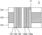
도 10d 및 도 11을 참조하면, 셀 홀들(H)의 측벽에 보호막(131)이 형성된다. 보호막(131)은 실리콘 산화막일 수 있다. 보호막(131) 상에 전하 저장막(133)이 형성된다. 전하 저장막(133)은 전하 트랩막 또는 도전성 나노 입자를 포함하는 절연막일 수 있다. 전하 트랩막은, 예를 들면 실리콘 질화막을 포함할 수 있다. 터널 절연막(132)이 전하 저장막(133) 상에 형성된다. 터널 절연막(132)은 실리콘 산화막일 수 있다. 보호막(131), 터널 절연막(132), 및 전하 저장막(133)은 ALD 또는 CVD 방법으로 형성될 수 있다.Referring to FIG. 10d and FIG. 11, a protective film (131) is formed on the sidewalls of the cell holes (H). The protective film (131) may be a silicon oxide film. A charge storage film (133) is formed on the protective film (131). The charge storage film (133) may be a charge trap film or an insulating film including conductive nanoparticles. The charge trap film may include, for example, a silicon nitride film. A tunnel insulating film (132) is formed on the charge storage film (133). The tunnel insulating film (132) may be a silicon oxide film. The protective film (131), the tunnel insulating film (132), and the charge storage film (133) may be formed by an ALD or CVD method.
터널 절연막(132) 상에 제1 서브 반도체막(135a)이 형성될 수 있다. 제1 서브 반도체막(135a)을 이방성 식각하여, 기판(110)을 노출한다. 제1 서브 반도체막(135a)은 터널 절연막(132)의 측벽에만 남겨진 스페이서막으로 변화될 수 있다. 제1 서브 반도체막(135a) 상에 제2 서브 반도체막(135b)이 형성될 수 있다. 제2 서브 반도체막(135b)은 기판(110)과 접촉한다. 제1 및 제2 서브 반도체막들(135a, 135b)은 ALD 또는 CVD 방법으로 형성될 수 있다. 제1 및 제2 서브 반도체막들(135a, 135b)은 비정질 실리콘막일 수 있다.A first sub-semiconductor film (135a) may be formed on a tunnel insulating film (132). The first sub-semiconductor film (135a) is anisotropically etched to expose the substrate (110). The first sub-semiconductor film (135a) may be changed into a spacer film that remains only on a sidewall of the tunnel insulating film (132). A second sub-semiconductor film (135b) may be formed on the first sub-semiconductor film (135a). The second sub-semiconductor film (135b) is in contact with the substrate (110). The first and second sub-semiconductor films (135a, 135b) may be formed by an ALD or CVD method. The first and second sub-semiconductor films (135a, 135b) may be amorphous silicon films.
도 10e 및 도 12를 참조하면, 열처리 공정이 수행되어, 제1 및 제2 서브 반도체막들(135a, 135b)이 반도체막(135)으로 변화될 수 있다. 반도체막(135)은 폴리 실리콘막 또는 결정질 실리콘막일 수 있다.Referring to FIG. 10e and FIG. 12, a heat treatment process may be performed so that the first and second sub-semiconductor films (135a, 135b) may be changed into a semiconductor film (135). The semiconductor film (135) may be a polysilicon film or a crystalline silicon film.
반도체막(135)은 셀 홀들(H)을 완전히 채우지 않도록 형성되고, 반도체막(135) 상에 절연 물질이 형성되어 셀 홀들(H)을 완전하게 채울 수 있다. 반도체막 및 절연 물질은 평탄화되어, 최상층의 절연막을 노출할 수 있다. 이에 따라 그 내부의 빈속이 충진 절연막(137)으로 채워진, 실린더 형의 반도체 기둥들(PL)이 형성될 수 있다. 반도체 기둥들(PL)은 제1 도전형의 반도체막일 수 있다. 도시된 것과는 달리, 반도체막은 셀 홀들(H)을 채우도록 형성될 수 있다. 이 경우, 충진 절연막은 요구되지 않을 수 있다.The semiconductor film (135) is formed so as not to completely fill the cell holes (H), and an insulating material is formed on the semiconductor film (135) to completely fill the cell holes (H). The semiconductor film and the insulating material may be planarized to expose the uppermost insulating film. Accordingly, cylindrical semiconductor pillars (PL) may be formed, the empty spaces therein being filled with a filling insulating film (137). The semiconductor pillars (PL) may be a semiconductor film of the first conductivity type. Unlike what is illustrated, the semiconductor film may be formed so as to fill the cell holes (H). In this case, a filling insulating film may not be required.
셀 기둥들(PL)의 상부는 리세스되어, 최상층의 절연막보다 낮게 될 수 있다. 셀 기둥들(PL)이 리세스된 셀 홀들(H) 내에 도전 패턴들(136)이 형성될 수 있다. 도전 패턴들(136)은 도핑된 폴리 실리콘 또는 금속일 수 있다. 도전 패턴들(136) 및 셀 기둥들(PL)의 윗부분에 제2 도전형의 불순물 이온을 주입하여, 드레인 영역들(D)이 형성될 수 있다. 제2 도전형은 예를 들면 N형일 수 있다.The upper portions of the cell pillars (PL) may be recessed to be lower than the uppermost insulating film. Conductive patterns (136) may be formed in the cell holes (H) in which the cell pillars (PL) are recessed. The conductive patterns (136) may be doped polysilicon or a metal. Impurity ions of a second conductive type may be injected into the upper portions of the conductive patterns (136) and the cell pillars (PL), thereby forming drain regions (D). The second conductive type may be, for example, N-type.
도 10f를 참조하면, 버퍼 유전막(122), 희생막들(123) 및 절연막들(124)을 연속적으로 패터닝하여, 서로 이격되고 제1 방향으로 연장되고 기판(110)을 노출하는, 분리영역들(121)이 형성된다. 패터닝된 절연막들(124)은 절연 패턴들(125)이 된다. 상기 패터닝에 의하여 상기 필러(F')의 가장자리 일부가 함께 제거됨으로써 필러(F)를 얻을 수 있다. 그 결과 추후 접지 선택 라인(GSL)이 형성되는 위치의 희생막들이 서로 분리될 수 있다.Referring to FIG. 10f, the buffer dielectric film (122), the sacrificial films (123), and the insulating films (124) are sequentially patterned to form separation regions (121) that are spaced apart from each other, extend in the first direction, and expose the substrate (110). The patterned insulating films (124) become insulating patterns (125). By the patterning, a portion of the edge of the filler (F') is removed together, thereby obtaining the filler (F). As a result, the sacrificial films at the location where the ground selection line (GSL) is to be formed later can be separated from each other.
그전에, 분리영역들(121) 사이에서 최상층의 절연막 및 희생막을 패터닝하여, 오프닝(127)을 형성할 수 있다. 오프닝(127)은 분리영역들(121) 사이에서 제1 방향(D1)으로 연장하여 최상층의 희생막을 두개로 나눌 수 있다. 오프닝 (127) 내에 절연막(예를 들어, 실리콘 산화막)이 채워질 수 있다.Before that, the uppermost insulating film and sacrificial film can be patterned between the separation regions (121) to form an opening (127). The opening (127) can extend in the first direction (D1) between the separation regions (121) to divide the uppermost sacrificial film into two. An insulating film (e.g., a silicon oxide film) can be filled within the opening (127).
도 10g를 참조하면, 분리영역들(121)에 노출된 희생막들(123)을 선택적으로 제거하여 리세스 영역(126)을 형성한다. 리세스 영역(126)은 희생막들(123)이 제거된 영역에 해당되고, 셀 기둥들(PL) 및 절연 패턴들(125)에 의하여 정의된다. 희생막들(123)이 실리콘 질화막 또는 실리콘 산질화막을 포함하는 경우, 희생막들의 제거 공정은 인산을 포함하는 식각 용액을 사용하여 수행될 수 있다. 리세스 영역(126)에 의하여 셀 기둥들(PL)의 측벽의 일부분들이 노출된다.Referring to FIG. 10g, sacrificial films (123) exposed to the separation regions (121) are selectively removed to form recessed regions (126). The recessed regions (126) correspond to regions where the sacrificial films (123) are removed, and are defined by the cell pillars (PL) and the insulating patterns (125). When the sacrificial films (123) include a silicon nitride film or a silicon oxynitride film, the process of removing the sacrificial films can be performed using an etching solution containing phosphoric acid. Parts of the sidewalls of the cell pillars (PL) are exposed by the recessed regions (126).
보호막(131)은, 희생막들(123)의 제거를 위한 식각 용액에 의하여 전하 저장막(133)이 손상되는 것을 방지할 수 있다. 리세스 영역(126)에 의하여 노출된 보호막(131)은 선택적으로 제거될 수 있다. 보호막(131)이 실리콘 산화막인 경우, 보호막(131)은, 예를 들어 불산을 포함하는 식각 용액에 의하여 제거될 수 있다. 이에 따라 리세스 영역(126)은 전하 저장막(133)의 일부분을 노출할 수 있다.The protective film (131) can prevent the charge storage film (133) from being damaged by an etching solution for removing the sacrificial films (123). The protective film (131) exposed by the recessed region (126) can be selectively removed. When the protective film (131) is a silicon oxide film, the protective film (131) can be removed by an etching solution containing, for example, hydrofluoric acid. Accordingly, the recessed region (126) can expose a portion of the charge storage film (133).
전술한 셀 홀들(H)의 형성을 용이하게 하기 위하여, 희생막들(123)과 절연막들(124)의 스택의 전체 높이를 줄이는 것이 바람직하다. 이에 따라, 셀 홀들(H)의 종횡비(aspect ratio)를 줄여, 희생막들(123)과 절연막들(124)의 스택의 식각이 용이하게 할 수 있다. 동일한 적층수에서, 스택의 전체 높이를 줄이는 것은 희생막들(123)의 두께 및/또는 절연막들(124)의 두께를 줄이는 것을 요구한다.In order to facilitate the formation of the aforementioned cell holes (H), it is desirable to reduce the overall height of the stack of sacrificial films (123) and insulating films (124). Accordingly, the aspect ratio of the cell holes (H) can be reduced, thereby facilitating the etching of the stack of sacrificial films (123) and insulating films (124). With the same number of layers, reducing the overall height of the stack requires reducing the thickness of the sacrificial films (123) and/or the thickness of the insulating films (124).
도 10h를 참조하면, 리세스 영역(126) 내에 블로킹 절연막(134)이 형성될 수 있다. 블로킹 절연막(134)은 리세스 영역(126)에 노출된 절연 패턴들(125)의 상부면 및 하부면, 그리고 전하저장막(133) 상에 콘포말하게 형성될 수 있다. 블로킹 절연막(134)은 고유전막(예를 들면, 알루미늄 산화막 또는 하프늄 산화막)을 포함할 수 있다. 블로킹 절연막은 복수의 박막들로 구성되는 다층막일 수 있다. 예를 들면, 블로킹 절연막은 알루미늄 산화막 및 실리콘 산화막을 포함할 수 있으며, 알루미늄 산화막 및 실리콘 산화막의 적층 순서는 다양할 수 있다. 블로킹 유전막(134)은 단차도포성이 우수한 원자층 증착 공정 및/또는 화학 기상 증착 공정에 의하여 형성될 수 있다.Referring to FIG. 10h, a blocking insulating film (134) may be formed in the recess region (126). The blocking insulating film (134) may be conformally formed on the upper and lower surfaces of the insulating patterns (125) exposed to the recess region (126) and on the charge storage film (133). The blocking insulating film (134) may include a high-k dielectric film (for example, an aluminum oxide film or a hafnium oxide film). The blocking insulating film may be a multilayer film composed of a plurality of thin films. For example, the blocking insulating film may include an aluminum oxide film and a silicon oxide film, and the stacking order of the aluminum oxide film and the silicon oxide film may vary. The blocking dielectric film (134) may be formed by an atomic layer deposition process and/or a chemical vapor deposition process having excellent step coating properties.
이어서, 블로킹 절연막(134) 상에 도전막(140)이 형성된다. 도전막(140)은 도핑된 실리콘막, 금속막, 금속 질화막 및 금속 실리사이드막 중의 적어도 하나를 포함할 수 있다. 도전막(140)은 CVD 또는 ALD 방법에 의하여 형성될 수 있다. 일 예로, 도전막(140)은 배리어막, 및 상기 배리어막 상의 금속막을 포함할 수 있다. 상기 배리어막은 금속 질화막(예를 들어, 티타늄 질화막)일 수 있다. 상기 금속막은 예를 들어, 텅스텐막일 수 있다. 다른 예로, 상기 도전막(140)은 폴리실리콘막, 및 폴리실리콘막 상의 실리사이드막을 포함할 수 있다. 이 경우, 상기 도전막(140)을 형성하는 것은 폴리실리콘막을 형성하고, 상기 분리 영역(121)에 인접한 폴리실리콘막의 일부를 제거하여 폴리실리콘막을 리세스하고, 리세스된 폴리실리콘막 상에 금속막을 형성하고, 금속막을 열처리하고, 그리고 미반응 금속막을 제거하는 것을 포함할 수 있다. 실리사이드막을 위한 금속막은 텅스텐, 티타늄, 코발트, 또는 니켈을 포함할 수 있다.Next, a conductive film (140) is formed on the blocking insulating film (134). The conductive film (140) may include at least one of a doped silicon film, a metal film, a metal nitride film, and a metal silicide film. The conductive film (140) may be formed by a CVD or ALD method. As an example, the conductive film (140) may include a barrier film and a metal film on the barrier film. The barrier film may be a metal nitride film (for example, a titanium nitride film). The metal film may be, for example, a tungsten film. As another example, the conductive film (140) may include a polysilicon film and a silicide film on the polysilicon film. In this case, forming the conductive film (140) may include forming a polysilicon film, removing a portion of the polysilicon film adjacent to the isolation region (121) to recess the polysilicon film, forming a metal film on the recessed polysilicon film, heat-treating the metal film, and removing the unreacted metal film. The metal film for the silicide film may include tungsten, titanium, cobalt, or nickel.
도 13은 도 10h의 C 부분을 상세하게 나타낸 부분 확대도이다.Figure 13 is an enlarged partial view showing details of portion C of Figure 10h.
도 13을 참조하면, 블로킹 절연막(134)만이 리세스 영역(126) 내에 형성되고 터널 절연막(132)과 전하 저장막(133)은 셀 홀들(H) 내에 형성될 수 있다.Referring to FIG. 13, only the blocking insulating film (134) can be formed within the recess region (126), and the tunnel insulating film (132) and the charge storage film (133) can be formed within the cell holes (H).
일부 실시예들에 있어서, 정보저장 요소(130)를 구성하는 터널 절연막(132), 전하 저장막(133), 및 블로킹 절연막(134) 모두가 리세스 영역(126, 도 10g 참조) 내에 형성될 수 있다. 이 경우, 보호막(131)은 형성되지 않을 수 있다. 도 10d 내지 도 10e의 공정 단계에서, 셀 홀들(H) 내에 보호막(131), 전하저장막(133), 및 터널 절연막(132)의 형성 없이, 셀 기둥들(PL)이 형성될 수 있다. 셀 기둥들(PL)은 셀 홀들(H) 내에 반도체막을 증착함으로써 형성될 수 있다. 이후, 도 10h의 공정 단계에서, 리세스 영역(126) 내에 터널 절연막(132), 전하 저장막(133), 및 블로킹 절연막(134)이 순서대로 형성될 수 있다. 이후, 블로킹 절연막(134) 상에 도전막(140)이 형성될 수 있다.In some embodiments, the tunnel insulating film (132), the charge storage film (133), and the blocking insulating film (134) constituting the information storage element (130) may all be formed within the recessed region (126, see FIG. 10g). In this case, the passivation film (131) may not be formed. In the process steps of FIGS. 10d to 10e, the cell pillars (PL) may be formed within the cell holes (H) without forming the passivation film (131), the charge storage film (133), and the tunnel insulating film (132). The cell pillars (PL) may be formed by depositing a semiconductor film within the cell holes (H). Thereafter, in the process step of FIG. 10h, the tunnel insulating film (132), the charge storage film (133), and the blocking insulating film (134) may be sequentially formed within the recessed region (126). Afterwards, a conductive film (140) can be formed on the blocking insulating film (134).
일부 실시예들에 있어서, 전하 저장막(133), 및 블로킹 절연막(134)이 리세스 영역(126) 내에 형성될 수 있다. 도 10d 내지 도 10e의 공정 단계에서, 셀 홀들(H) 내에 보호막(131) 및 터널 절연막(132)의 형성 후, 셀 기둥들(PL)이 형성될 수 있다. 셀 기둥들(PL)은 도 10d 내지 도 10e의 공정 단계에서와 유사한 방법으로 형성될 수 있다. 이후, 도 10h의 공정 단계에서, 리세스 영역(126) 내에 전하 저장막(133), 및 블로킹 절연막(134)이 순서대로 형성될 수 있다. 이후, 블로킹 절연막(134) 상에 도전막(140)이 형성될 수 있다.In some embodiments, the charge storage film (133) and the blocking insulating film (134) may be formed in the recessed region (126). In the process steps of FIGS. 10d to 10e, after the formation of the protective film (131) and the tunnel insulating film (132) in the cell holes (H), cell pillars (PL) may be formed. The cell pillars (PL) may be formed in a similar manner as in the process steps of FIGS. 10d to 10e. Thereafter, in the process step of FIG. 10h, the charge storage film (133) and the blocking insulating film (134) may be sequentially formed in the recessed region (126). Thereafter, the conductive film (140) may be formed on the blocking insulating film (134).
일부 실시예들에 있어서, 정보저장 요소(130)를 구성하는 터널 절연막(132), 전하 저장막(133), 및 블로킹 절연막(134) 모두가 셀 홀들(H) 내에 형성될 수 있다. 도 10d 내지 도 10e의 공정 단계에서, 셀 홀들(H) 내에 보호막(131), 블로킹 절연막(134), 전하 저장막(133), 및 터널 절연막(132)이 순차적으로 형성된다. 터널 절연막(132) 상에 셀 기둥들(PL)이 형성될 수 있다. 셀 기둥들(PL)은 도 10d 내지 도 10e의 공정 단계에서와 유사한 방법으로 형성될 수 있다. 이후, 도 10h의 공정 단계에서, 리세스 영역(126) 내에 도전막(140)이 형성될 수 있다.In some embodiments, all of the tunnel insulating film (132), the charge storage film (133), and the blocking insulating film (134) constituting the information storage element (130) may be formed within the cell holes (H). In the process steps of FIGS. 10d to 10e, the protective film (131), the blocking insulating film (134), the charge storage film (133), and the tunnel insulating film (132) are sequentially formed within the cell holes (H). Cell pillars (PL) may be formed on the tunnel insulating film (132). The cell pillars (PL) may be formed in a similar manner as in the process steps of FIGS. 10d to 10e. Thereafter, in the process step of FIG. 10h, a conductive film (140) may be formed within the recess region (126).
일부 실시예들에 있어서, 정보저장 요소(130)는 가변저항 패턴일 수 있다. 가변저항 패턴은 그것의 저항이 변화될 수 있는, 가변저항 특성을 갖는 물질들 중의 적어도 하나를 포함할 수 있다.In some embodiments, the information storage element (130) may be a variable resistance pattern. The variable resistance pattern may include at least one of materials having variable resistance properties, the resistance of which may be changed.
일 예로, 정보저장 요소(130)는 그것에 인접한 전극을 통과하는 전류에 의해 발생하는 열에 의해 그것의 전기적 저항이 변화될 수 있는 물질(예를 들면, 상변화 물질)을 포함할 수 있다. 상변화 물질은 안티몬(antimony, Sb), 텔루리움(tellurium, Te) 및 셀레늄(selenium, Se) 중의 적어도 한 가지를 포함할 수 있다. 예를 들면, 상변화 물질은, 텔루리움(Te)은 대략 20 원자 퍼센트 내지 대략 80 원자 퍼센트의 농도를 갖고, 안티몬(Sb)은 대략 5 원자 퍼센트 내지 대략 50 원자 퍼센트의 농도를 갖고, 나머지는 게르마늄(Ge)인 칼코겐 화합물을 포함할 수 있다. 이에 더하여, 상변화 물질은, 불순물로서, N, O, C, Bi, In, B, Sn, Si, Ti, Al, Ni, Fe, Dy 및 La 중의 적어도 한 가지를 포함할 수 있다. 또는, 가변저항 패턴은 GeBiTe, InSb, GeSb 및 GaSb 중의 한가지로 형성될 수도 있다.For example, the information storage element (130) may include a material (e.g., a phase change material) whose electrical resistance can be changed by heat generated by a current passing through an electrode adjacent to it. The phase change material may include at least one of antimony (Sb), tellurium (Te), and selenium (Se). For example, the phase change material may include a chalcogenide having tellurium (Te) in a concentration of about 20 atomic percent to about 80 atomic percent, antimony (Sb) in a concentration of about 5 atomic percent to about 50 atomic percent, and the remainder being germanium (Ge). In addition, the phase change material may include at least one of N, O, C, Bi, In, B, Sn, Si, Ti, Al, Ni, Fe, Dy, and La as an impurity. Alternatively, the variable resistance pattern may be formed from one of GeBiTe, InSb, GeSb, and GaSb.
다른 예로, 정보저장 요소(130)는 그것을 통과하는 전류에 의한 스핀 전달 과정을 이용하여 그것의 전기적 저항이 변화될 수 있는 박막 구조를 갖도록 형성될 수 있다. 정보저장 요소(130)는 자기-저항(magnetoresistance) 특성을 보이도록 구성되는 박막 구조를 가질 수 있으며, 적어도 하나의 강자성 물질들 및/또는 적어도 하나의 반강자성 물질들을 포함할 수 있다.As another example, the information storage element (130) may be formed to have a thin film structure whose electrical resistance can be changed by utilizing a spin transfer process by a current passing through it. The information storage element (130) may have a thin film structure configured to exhibit magnetoresistance characteristics and may include at least one ferromagnetic material and/or at least one antiferromagnetic material.
또 다른 예로, 정보저장 요소(130)는 페로브스카이트(perovskite) 화합물들 또는 전이금속 산화물들 중의 적어도 하나를 포함할 수 있다. 예를 들면, 정보저장 요소(135)는 니오븀 산화물(niobium oxide), 티타늄 산화물(titanium oxide), 니켈 산화물(nikel oxide), 지르코늄 산화물(zirconium oxide), 바나듐 산화물(vanadium oxide), PCMO((Pr,Ca)MnO3), 스트론튬-티타늄 산화물(strontium-titanium oxide), 바륨-스트론튬-티타늄 산화물(barium-strontium-titanium oxide), 스트론튬-지르코늄 산화물(strontium-zirconium oxide), 바륨-지르코늄 산화물(barium-zirconium oxide), 또는 바륨-스트론튬-지르코늄 산화물(barium-strontium-zirconium oxide) 등에서 적어도 하나를 포함할 수 있다.As another example, the information storage element (130) may include at least one of perovskite compounds or transition metal oxides. For example, the information storage element (135) may include at least one of niobium oxide, titanium oxide, nickel oxide, zirconium oxide, vanadium oxide, PCMO ((Pr,Ca)MnO3 ), strontium-titanium oxide, barium-strontium-titanium oxide, strontium-zirconium oxide, barium-zirconium oxide, or barium-strontium-zirconium oxide.
이러한 경우, 셀 기둥들(PL)은 도전 기둥들일 수 있다. 셀 기둥들(PL)은 도전성 물질로 형성될 수 있다. 도전성 물질은, 예를 들면 도핑된 반도체, 금속, 도전성 금속 질화물, 실리사이드, 또는 (탄소 나노 튜브 또는 그래핀 등과 같은) 나노 구조체 중의 적어도 하나를 포함할 수 있다.In this case, the cell pillars (PL) can be conductive pillars. The cell pillars (PL) can be formed of a conductive material. The conductive material can include, for example, at least one of a doped semiconductor, a metal, a conductive metal nitride, a silicide, or a nanostructure (such as a carbon nanotube or graphene).
이러한 구조를 위하여, 도 10d 내지 도 10e의 공정 단계에서, 셀 홀들(H) 내에 보호막(131) 및 정보저장 요소(130)가 순차적으로 형성된다. 정보저장 요소(130) 상에 셀 기둥들(PL)이 형성될 수 있다. 셀 기둥들(PL)은 도전성 물질을 증착함에 의하여 형성될 수 있다. 이후, 도 10h의 공정 단계에서, 리세스 영역(126) 내에 도전막(140)이 형성될 수 있다.For this structure, in the process steps of FIGS. 10d to 10e, a protective film (131) and an information storage element (130) are sequentially formed within the cell holes (H). Cell pillars (PL) may be formed on the information storage element (130). The cell pillars (PL) may be formed by depositing a conductive material. Thereafter, in the process step of FIG. 10h, a conductive film (140) may be formed within the recess region (126).
계속하여 도 10i를 참조하면, 리세스 영역(126)의 외부에 형성된 도전막(140)이 제거된다. 이에 따라, 리세스 영역(126)의 내에 수평 전극들이 형성된다. 수평전극들은 접지 선택 라인(GSL), 워드 라인들(WL0 내지 WL3), 더미 워드 라인들(DM1, DM2) 및 스트링 선택 라인들(SSL1, SSL2)을 포함할 수 있다. 상부 스트링 선택 라인들(SSL1, SSL2)은 두 개로 분리될 수 있고, 이들은 제1 방향(D1)으로 연장한다.Referring still to FIG. 10i, the conductive film (140) formed outside the recess region (126) is removed. Accordingly, horizontal electrodes are formed inside the recess region (126). The horizontal electrodes may include a ground selection line (GSL), word lines (WL0 to WL3), dummy word lines (DM1, DM2), and string selection lines (SSL1, SSL2). The upper string selection lines (SSL1, SSL2) may be separated into two, which extend in the first direction (D1).
분리영역들(121)에 형성된 도전막(140)이 제거되어 기판(110)이 노출될 수 있다. 노출된 기판(110)에 제2 도전형의 불순물 이온이 고농도로 제공되어 공통 소오스 라인들(CSL)이 형성될 수 있다.The conductive film (140) formed in the separation regions (121) may be removed to expose the substrate (110). A high concentration of second conductive type impurity ions may be provided to the exposed substrate (110) to form common source lines (CSL).
분리영역들(121)을 채우는 분리 절연막(120)이 형성된다. 제2 방향으로 정렬된 셀 기둥들(PL)은 하나의 상부 배선(BL1 또는 BL2)에 공통으로 연결될 수 있다. (도 3 참조)A separation insulating film (120) is formed to fill the separation areas (121). The cell columns (PL) aligned in the second direction can be commonly connected to one upper wiring (BL1 or BL2). (See FIG. 3)
도 14는 본 발명의 일 실시예에 따른 반도체 메모리 장치를 셀 기둥을 중심으로 나타낸 측단면도이다. 도 14는 셀 홀(H)들의 바닥에 채널 콘택 영역(151)이더 형성되는 점에서 도 3에 나타낸 실시예와 차이가 있다. 이하에서는 도 3의 실시예와 공통되는 내용은 생략하고, 서로 상이한 사항을 중심으로 반도체 메모리 장치를 설명한다.Fig. 14 is a cross-sectional side view of a semiconductor memory device according to an embodiment of the present invention, centered on a cell pillar. Fig. 14 is different from the embodiment shown in Fig. 3 in that a channel contact region (151) is formed at the bottom of the cell holes (H). Hereinafter, common contents with the embodiment of Fig. 3 will be omitted, and the semiconductor memory device will be described focusing on the different contents.
도 14를 참조하면, 도 10c에서와 같이 셀 홀(H)을 형성한 후 상기 셀 홀(H)의 바닥에 노출된 기판(110) 상에 채널 콘택 영역(151)을 형성할 수 있다. 일부 실시예들에 있어서, 상기 채널 콘택 영역(151)은 노출된 기판(110)으로부터 선택적 에피택셜 성장(selective epitaxial growth, SEG)에 의하여 성장될 수 있다. 이 때, 상기 채널 콘택 영역(151)의 상부 표면의 레벨은 최하부에 있는 희생층(123)의 상부면보다 높도록 형성될 수 있다.Referring to FIG. 14, after forming a cell hole (H) as in FIG. 10c, a channel contact region (151) may be formed on a substrate (110) exposed at the bottom of the cell hole (H). In some embodiments, the channel contact region (151) may be grown from the exposed substrate (110) by selective epitaxial growth (SEG). At this time, the level of the upper surface of the channel contact region (151) may be formed to be higher than the upper surface of the sacrificial layer (123) at the lowermost portion.
이후, 이온 주입 공정에 의해 채널 콘택 영역(151)에 p형 불순물을 주입할 수 있다. 예를 들어, 상기 p형 불순물은 알루미늄(Al), 붕소(B), 인듐(In) 또는 칼륨(K)일 수 있고, 상기 p형 불순물의 농도는 5E16 내지 1E19 atoms/cm3의 범위일 수 있다. 이와는 달리, 상기 SEG 공정에 의해 채널 콘택 영역(151)을 성장시키는 과정에서 p형 불순물을 인시츄 도핑할 수도 있다.Thereafter, a p-type impurity may be implanted into the channel contact region (151) by an ion implantation process. For example, the p-type impurity may be aluminum (Al), boron (B), indium (In), or potassium (K), and the concentration of the p-type impurity may be in a range of 5E16 to 1E19 atoms/cm3 . Alternatively, the p-type impurity may be in-situ doped during the process of growing the channel contact region (151) by the SEG process.
이어서 도 10d 내지 도 10f에서와 같이 셀 기둥(PL)들을 형성하고 분리 영역을 형성한 후 도 10g에서와 같이 희생막들(123)을 제거하고, 채널 콘택 영역(151)의 측벽 상에 열산화 공정(thermal oxidation process)을 수행하여 보조 게이트 절연막(153)을 형성할 수 있다. 상기 보조 게이트 절연막(153)은 상기 SEG 성장된 채널 콘택 영역(151)의 일부가 열산화되어 형성된 열산화막일 수 있다. 다만 상기 보조 게이트 절연막(153)의 형성을 위한 열산화 공정은 생략될 수 있다.Subsequently, as shown in FIGS. 10d to 10f, cell pillars (PL) are formed and a separation region is formed, and then, as shown in FIG. 10g, the sacrificial films (123) are removed, and a thermal oxidation process is performed on the sidewall of the channel contact region (151) to form an auxiliary gate insulating film (153). The auxiliary gate insulating film (153) may be a thermal oxidation film formed by thermally oxidizing a portion of the SEG-grown channel contact region (151). However, the thermal oxidation process for forming the auxiliary gate insulating film (153) may be omitted.
이어서 도 10h 및 도 10i에 도시된 바와 같이 블로킹 절연막(134), 터널 절연막(132), 및 전하 저장막(133)을 형성하고 도전막(140)을 형성한 후, 분리영역들(121)을 채우는 분리 절연막(120)을 형성할 수 있다.Next, as shown in FIG. 10h and FIG. 10i, a blocking insulating film (134), a tunnel insulating film (132), and a charge storage film (133) are formed, and a conductive film (140) is formed, and then a separation insulating film (120) that fills the separation regions (121) can be formed.
도 15a 및 도 15b는 상기 국부 평탄화 영역(LPR)에 기판(110)이 부분적으로 융기되는 실시예를 순서에 따라 나타낸 측단면도들이다.FIGS. 15a and 15b are cross-sectional side views sequentially showing an example in which the substrate (110) is partially raised in the local flattening region (LPR).
도 15a를 참조하면, 기판(110)은 연결 영역(B)과 주변 회로 영역(C)을 포함할 수 있다. 특히, 주변 회로 영역(C)은 고전압의 전자 소자들이 형성되는 주변 회로 영역(HV)과 저전압의 전자 소자들이 형성되는 주변 회로 영역(LV)을 포함할 수 있다.Referring to FIG. 15a, the substrate (110) may include a connection region (B) and a peripheral circuit region (C). In particular, the peripheral circuit region (C) may include a peripheral circuit region (HV) in which high-voltage electronic components are formed and a peripheral circuit region (LV) in which low-voltage electronic components are formed.
주변 회로 영역(HV)에서는 전자 소자의 구동에 고전압이 이용되기 때문에 게이트 절연막이 상대적으로 두껍게 형성될 필요가 있고, 주변 회로 영역(LV)에서는 전자 소자의 구동에 저전압이 이용되기 때문에 게이트 절연막이 상대적으로 얇게 형성될 필요가 있다. 이를 위하여 주변 회로 영역(HV)의 상부 표면의 레벨이 주변 회로 영역(LV)의 상부 표면의 레벨보다 낮아지도록 할 필요가 있다.In the peripheral circuit area (HV), since a high voltage is used to drive electronic elements, the gate insulating film needs to be formed relatively thick, and in the peripheral circuit area (LV), since a low voltage is used to drive electronic elements, the gate insulating film needs to be formed relatively thin. To this end, it is necessary to make the level of the upper surface of the peripheral circuit area (HV) lower than the level of the upper surface of the peripheral circuit area (LV).
주변 회로 영역(HV)의 상부 표면의 레벨을 낮추기 위하여 주변 회로 영역(LV)을 덮는 식각 마스크(210)를 형성할 수 있다. 이 때, 연결 영역(B)에서 국부 평탄화 영역(LPR)에 대해서도 식각 마스크(210)를 형성한다.An etching mask (210) covering the peripheral circuit region (LV) can be formed to lower the level of the upper surface of the peripheral circuit region (HV). At this time, an etching mask (210) is also formed for the local planarization region (LPR) in the connection region (B).
도 15b를 참조하면, 이방성 식각을 수행하여 주변 회로 영역(HV)의 상부 표면의 레벨을 낮춘다. 이 때, 연결 영역(B)에서도 국부 평탄화 영역(LPR) 외의 부분에 대하여 이방성 식각이 수행되기 때문에 상대적으로 국부 평탄화 영역(LPR)이 그 외의 연결 영역(B)에 비하여 더 높은 레벨을 가지며 융기할 수 있다.Referring to Fig. 15b, anisotropic etching is performed to lower the level of the upper surface of the peripheral circuit region (HV). At this time, since anisotropic etching is performed on a portion other than the local planarization region (LPR) in the connection region (B), the local planarization region (LPR) can be raised to a relatively higher level than the other connection regions (B).
상기 연결 영역(B)에서의 노출된 영역과 상기 주변 회로 영역(HV)이 동시에 식각되기 때문에, 상기 연결 영역(B) 내의 국부 평탄화 영역(LPR)에서 융기된 높이는 상기 주변 회로 영역(HV)의 상부 표면의 레벨과 상기 주변 회로 영역(LV)의 상부 표면의 레벨의 차이와 실질적으로 동일할 수 있다.Since the exposed area in the above connection area (B) and the peripheral circuit area (HV) are etched simultaneously, the raised height in the local planarization area (LPR) within the connection area (B) can be substantially equal to the difference between the level of the upper surface of the peripheral circuit area (HV) and the level of the upper surface of the peripheral circuit area (LV).
이와 같이 수행하는 경우 별도의 공정 추가 없이 국부 평탄화 영역(LPR)의 빈 공간을 적어도 부분적으로 필링할 수 있기 때문에 저렴하게 반도체 메모리 장치를 제조하는 것이 가능하다.By performing this, it is possible to manufacture semiconductor memory devices inexpensively because the empty space in the local planarization region (LPR) can be at least partially filled without additional processes.
이어서, 상기 주변 회로 영역(HV)에 대하여 두꺼운 게이트 절연막(222)을 형성하고, 주변 회로 영역(LV) 및 연결 영역(B)에 대하여 얇은 게이트 절연막(224)을 형성할 수 있다.Next, a thick gate insulating film (222) can be formed for the peripheral circuit region (HV), and a thin gate insulating film (224) can be formed for the peripheral circuit region (LV) and the connection region (B).
일부 실시예들에 있어서, 상기 얇은 게이트 절연막(224)은 상기 연결 영역(B)과 도 15b에서는 미도시된 셀 어레이 영역에서 버퍼 유전막(122)으로서 작용할 수 있다.In some embodiments, the thin gate insulating film (224) may act as a buffer dielectric film (122) in the connection region (B) and a cell array region not shown in FIG. 15B.
도 15b에서와 같이 융기된 기판의 국부 평탄화 영역(LPR)이 형성된 이후의 공정은 도 10b 내지 도 10i 및 도 11 내지 14를 참조하여 설명한 바와 같기 때문에 추가적인 설명은 생략한다.The process after the local flattening region (LPR) of the raised substrate is formed as in Fig. 15b is the same as that described with reference to Figs. 10b to 10i and Figs. 11 to 14, so further description is omitted.
도 16은 본 발명의 기술적 사상에 의한 실시예들에 따른 집적회로 소자를 모바일 시스템(1200)에 응용한 예를 나타내는 블록도이다.FIG. 16 is a block diagram showing an example of applying an integrated circuit device according to embodiments of the technical idea of the present invention to a mobile system (1200).
도 16을 참조하면, 모바일 시스템(1200)은 어플리케이션 프로세서(1210), 통신(connectivity)부(1220), 휘발성 메모리 소자(1230), 불휘발성 메모리 시스템(1240), 사용자 인터페이스(1250), 및 파워 서플라이(1260)를 포함한다.Referring to FIG. 16, the mobile system (1200) includes an application processor (1210), a connectivity unit (1220), a volatile memory device (1230), a nonvolatile memory system (1240), a user interface (1250), and a power supply (1260).
상기 모바일 시스템(1200)은 휴대폰(Mobile Phone), 스마트 폰(Smart Phone), 개인 정보 단말기(Personal Digital Assistant: PDA), 휴대형 멀티미디어 플레이어(Portable Multimedia Player: PMP), 디지털 카메라(Digital Camera), 음악 재생기(Music Player), 휴대용 게임 콘솔(Portable Game Console), 네비게이션(Navigation) 시스템 등과 같은 임의의 모바일 시스템일 수 있다.The above mobile system (1200) may be any mobile system such as a mobile phone, a smart phone, a personal digital assistant (PDA), a portable multimedia player (PMP), a digital camera, a music player, a portable game console, a navigation system, etc.
상기 어플리케이션 프로세서(1210)는 인터넷 브라우저, 게임, 동영상 등을 제공하는 어플리케이션들을 실행할 수 있다. 실시예에 따라서, 어플리케이션 프로세서(1210)는 하나의 프로세서 코어(Single Core)를 포함하거나, 복수의 프로세서 코어(Multi-Core)을 포함할 수 있다. 예를 들면, 어플리케이션 프로세서(1210)는 듀얼 코어(Dual-Core), 쿼드 코어(Quad-Core), 헥사 코어(Hexa-Core) 등의 멀티 코어(Multi-Core)를 포함할 수 있다. 또한, 상기 어플리케이션 프로세서(1210)는 내부 또는 외부에 위치한 캐시 메모리(Cache Memory)를 더 포함할 수 있다.The above application processor (1210) can execute applications that provide Internet browsers, games, videos, etc. According to an embodiment, the application processor (1210) may include one processor core (Single Core) or multiple processor cores (Multi-Core). For example, the application processor (1210) may include a multi-core such as a dual core, a quad core, a hexa-core, etc. In addition, the application processor (1210) may further include a cache memory located internally or externally.
상기 통신부(1220)는 외부 장치와 무선 통신 또는 유선 통신을 수행할 수 있다. 예를 들면, 통신부(1220)는 이더넷(Ethernet) 통신, 근거리 자기장 통신(Near Field Communication: NFC), 무선 식별(Radio Frequency Identification: RFID) 통신, 이동 통신(Mobile Telecommunication), 메모리 카드 통신, 범용 직렬 버스(Universal Serial Bus: USB) 통신 등을 수행할 수 있다. 예를 들면, 통신부(1220)는 베이스밴드 칩 셋(Baseband Chipset)을 포함할 수 있고, GSM, GPRS, WCDMA, HSxPA 등의 통신을 지원할 수 있다.The above communication unit (1220) can perform wireless communication or wired communication with an external device. For example, the communication unit (1220) can perform Ethernet communication, Near Field Communication (NFC), Radio Frequency Identification (RFID) communication, Mobile Telecommunication, memory card communication, Universal Serial Bus (USB) communication, etc. For example, the communication unit (1220) can include a baseband chipset and support communication such as GSM, GPRS, WCDMA, and HSxPA.
상기 휘발성 메모리 소자(1230)는 어플리케이션 프로세서(1210)에 의해 처리되는 데이터를 저장하거나, 동작 메모리(Working Memory)로서 작동할 수 있다. 예를 들면, 휘발성 메모리 소자(1230)는 DRAM (Dynamic Random Access Memory), SRAM (Static Random Access Memory), 모바일 DRAM, DDR SDRAM, LPDDR SDRAM, GDDR SDRAM, RDRAM 또는 이와 유사한 메모리로 구현될 수 있다.The above volatile memory device (1230) may store data processed by the application processor (1210) or operate as a working memory. For example, the volatile memory device (1230) may be implemented as a DRAM (Dynamic Random Access Memory), an SRAM (Static Random Access Memory), a mobile DRAM, a DDR SDRAM, an LPDDR SDRAM, a GDDR SDRAM, an RDRAM, or a similar memory.
상기 불휘발성 메모리 시스템(1240)은 메모리 컨트롤러(1241) 및 불휘발성 메모리 소자(1243)를 포함하고, 모바일 시스템(1200)을 부팅하기 위한 부트 이미지를 저장할 수 있다. 예를 들면, 불휘발성 메모리 소자(1143)는 EEPROM (Electrically Erasable Programmable Read-Only Memory), 플래시 메모리 (Flash Memory), PRAM (Phase Change Random Access Memory), RRAM (Resistance Random Access Memory), NFGM (Nano Floating Gate Memory), PoRAM (Polymer Random Access Memory), MRAM (Magnetic Random Access Memory), FRAM (Ferroelectric Random Access Memory) 또는 이와 유사한 메모리로 구현될 수 있다. 상기 불휘발성 메모리 소자(1243)는 전술한 도 4a 내지 도 9를 참조하여 설명한 집적회로 소자 중 적어도 하나를 포함할 수 있다.The nonvolatile memory system (1240) includes a memory controller (1241) and a nonvolatile memory element (1243), and can store a boot image for booting the mobile system (1200). For example, the nonvolatile memory element (1143) can be implemented as an Electrically Erasable Programmable Read-Only Memory (EEPROM), a Flash Memory, a Phase Change Random Access Memory (PRAM), a Resistance Random Access Memory (RRAM), a Nano Floating Gate Memory (NFGM), a Polymer Random Access Memory (PoRAM), a Magnetic Random Access Memory (MRAM), a Ferroelectric Random Access Memory (FRAM), or a similar memory. The nonvolatile memory element (1243) can include at least one of the integrated circuit elements described with reference to FIGS. 4A to 9 described above.
상기 사용자 인터페이스(1250)는 키패드, 터치 스크린과 같은 하나 이상의 입력 장치, 및/또는 스피커, 디스플레이 장치와 같은 하나 이상의 출력 장치를 포함할 수 있다.The user interface (1250) may include one or more input devices, such as a keypad, a touch screen, and/or one or more output devices, such as a speaker, a display device.
상기 파워 서플라이(1260)는 모바일 시스템(1200)의 동작 전압을 공급할 수 있다. 또한, 상기 모바일 시스템(1200)은 카메라 이미지 프로세서(Camera Image Processor: CIS)를 더 포함할 수 있고, 메모리 카드(Memory Card), 솔리드 스테이트 드라이브(Solid State Drive: SSD), 하드 디스크 드라이브(Hard Disk Drive: HDD), 씨디롬(CD-ROM) 등과 같은 저장 장치를 더 포함할 수 있다.The above power supply (1260) can supply an operating voltage of the mobile system (1200). In addition, the mobile system (1200) can further include a camera image processor (CIS) and a storage device such as a memory card, a solid state drive (SSD), a hard disk drive (HDD), a CD-ROM, etc.
상기 모바일 시스템(1200)은 다양한 형태들의 패키지를 이용하여 실장될 수 있다. 예를 들면, PoP (Package on Package), BGAs (Ball grid arrays), CSPs (Chip scale packages), PLCC (Plastic Leaded Chip Carrier), PDIP (Plastic Dual In-Line Package), Die in Waffle Pack, Die in Wafer Form, COB (Chip On Board), CERDIP (Ceramic Dual In-Line Package), MQFP (Plastic Metric Quad Flat Pack), TQFP (Thin Quad Flat-Pack), SOIC (Small Outline Integrated Circuit), SSOP (Shrink Small Outline Package), TSOP (Thin Small Outline Package), TQFP (Thin Quad Flat-Pack), SIP (System In Package), MCP (Multi Chip Package), WFP (Wafer-level Fabricated Package), WSP (Wafer-Level Processed Stack Package) 등과 같은 패키지들을 이용하여 실장될 수 있다.The above mobile system (1200) can be mounted using various types of packages. For example, it can be mounted using packages such as PoP (Package on Package), BGAs (Ball grid arrays), CSPs (Chip scale packages), PLCC (Plastic Leaded Chip Carrier), PDIP (Plastic Dual In-Line Package), Die in Waffle Pack, Die in Wafer Form, COB (Chip On Board), CERDIP (Ceramic Dual In-Line Package), MQFP (Plastic Metric Quad Flat Pack), TQFP (Thin Quad Flat-Pack), SOIC (Small Outline Integrated Circuit), SSOP (Shrink Small Outline Package), TSOP (Thin Small Outline Package), TQFP (Thin Quad Flat-Pack), SIP (System In Package), MCP (Multi Chip Package), WFP (Wafer-level Fabricated Package), WSP (Wafer-Level Processed Stack Package), etc.
이상에서 살펴본 바와 같이 본 발명의 실시예들에 대해 상세히 기술되었지만, 본 발명이 속하는 기술분야에 있어서 통상의 지식을 가진 사람이라면, 첨부된 청구 범위에 정의된 본 발명의 정신 및 범위를 벗어나지 않으면서 본 발명을 여러 가지로 변형하여 실시할 수 있을 것이다. 따라서 본 발명의 앞으로의 실시예들의 변경은 본 발명의 기술을 벗어날 수 없을 것이다.Although the embodiments of the present invention have been described in detail above, it will be apparent to those skilled in the art that various modifications may be made to the present invention without departing from the spirit and scope of the present invention as defined in the appended claims. Accordingly, modifications to future embodiments of the present invention will not be able to depart from the technology of the present invention.
110: 기판121: 분리 영역
122: 버퍼 유전막123: 희생각
125: 절연 패턴130: 정보저장 요소110: Substrate 121: Separation area
122: Buffer dielectric film 123: Sacrificial angle
125: Insulation pattern 130: Information storage element
Claims (10)
Translated fromKorean상기 셀 영역에서 상기 기판 상에 적층되고 상기 연결 영역까지 연장되는 복수개의 제 1 워드 라인들을 포함하는 제 1 워드 라인 스택;
상기 셀 영역에서 상기 기판 상에 적층되고 상기 연결 영역까지 연장되는 복수개의 제 2 워드 라인들을 포함하고, 상기 제 1 워드 라인 스택에 인접한 제 2 워드 라인 스택;
상기 셀 영역에서, 상기 복수 개의 워드라인들에 결합되어 상기 기판에 연결된 수직 채널들;
상기 제 1 워드 라인 스택의 워드 라인 및 그와 대응되는 상기 제 2 워드 라인 스택의 워드 라인을 연결하는 브릿지 영역; 및
상기 브릿지 영역의 하부에 제공된 국부 평탄화 영역;을 포함하며,
상기 국부 평탄화 영역에서의 기판은 상기 제 1 워드 라인 스택의 하부의 기판에 비하여 융기되어 있는 것을 특징으로 하는 반도체 메모리 장치.A substrate having a cell region and a connection region;
A first word line stack comprising a plurality of first word lines stacked on the substrate in the cell region and extending to the connection region;
A second word line stack comprising a plurality of second word lines stacked on the substrate in the cell region and extending to the connection region, the second word line stack being adjacent to the first word line stack;
In the cell region, vertical channels coupled to the plurality of word lines and connected to the substrate;
a bridge region connecting a word line of the first word line stack and a corresponding word line of the second word line stack; and
A local flattening area provided at the lower portion of the above bridge area;
A semiconductor memory device, characterized in that the substrate in the above-mentioned local planarization region is raised compared to the substrate below the first word line stack.
상기 제 1 워드 라인들의 하부에 배치된 제 1 접지 선택 라인; 및
상기 제 2 워드 라인들의 하부에 배치된 제 2 접지 선택 라인;
을 더 포함하고,
상기 제 1 접지 선택 라인과 상기 제 2 접지 선택 라인은 상기 국부 평탄화 영역을 사이에 두고 이격된 것을 특징으로 하는 반도체 메모리 장치.In the first paragraph,
a first ground select line arranged below the first word lines; and
A second ground select line arranged below the second word lines;
Including more,
A semiconductor memory device, characterized in that the first ground selection line and the second ground selection line are spaced apart from each other with the local flattening region therebetween.
상기 국부 평탄화 영역에서의 기판은 상기 제 2 워드 라인 스택의 하부의 기판에 비하여 20Å 내지 300Å의 높이로 융기된 것을 특징으로 하는 반도체 메모리 장치.In the first paragraph,
A semiconductor memory device, characterized in that the substrate in the local planarization region is raised to a height of 20 Å to 300 Å compared to the substrate below the second word line stack.
상기 기판이,
저전압 트랜지스터를 갖는 저전압 주변 회로 영역; 및
고전압 트랜지스터를 갖는 고전압 주변 회로 영역;
을 더 포함하고,
상기 국부 평탄화 영역에서 상기 기판이 융기된 높이는 상기 저전압 주변 회로 영역의 기판과 상기 고전압 주변 회로 영역의 기판의 높이 차이와 실질적으로 동일한 것을 특징으로 하는 반도체 메모리 장치.In the first paragraph,
The above substrate,
A low-voltage peripheral circuit area having low-voltage transistors; and
High voltage peripheral circuit area having high voltage transistors;
Including more,
A semiconductor memory device, characterized in that the height of the substrate raised in the local flattening region is substantially the same as the height difference between the substrate in the low-voltage peripheral circuit region and the substrate in the high-voltage peripheral circuit region.
상기 셀 영역에서 상기 기판 상에 적층되고 상기 연결 영역까지 연장되는 복수개의 제 1 워드 라인들을 포함하는 제 1 워드 라인 스택;
상기 셀 영역에서 상기 기판 상에 적층되고 상기 연결 영역까지 연장되는 복수개의 제 2 워드 라인들을 포함하고, 상기 제 1 워드 라인 스택에 인접한 제 2 워드 라인 스택;
상기 셀 영역에서, 상기 복수 개의 워드라인들에 결합되어 상기 기판에 연결된 수직 채널들;
상기 제 1 워드 라인 스택의 워드 라인 및 그와 대응되는 상기 제 2 워드 라인 스택의 워드 라인을 연결하는 브릿지 영역; 및
상기 브릿지 영역의 하부에 제공된 국부 평탄화 영역;을 포함하며,
상기 국부 평탄화 영역은 상기 기판의 산화물 층에 의하여 적어도 부분적으로 매립되며,
상기 기판의 산화물 층은 상기 국부 평탄화 영역의 가장자리로 갈수록 두께가 얇아지는 형상을 갖는 것을 특징으로 하는 반도체 메모리 장치.A substrate having a cell region and a connection region;
A first word line stack comprising a plurality of first word lines stacked on the substrate in the cell region and extending to the connection region;
A second word line stack comprising a plurality of second word lines stacked on the substrate in the cell region and extending to the connection region, the second word line stack being adjacent to the first word line stack;
In the cell region, vertical channels coupled to the plurality of word lines and connected to the substrate;
a bridge region connecting a word line of the first word line stack and a corresponding word line of the second word line stack; and
A local flattening area provided at the lower portion of the above bridge area;
The above local flattening region is at least partially filled by an oxide layer of the substrate,
A semiconductor memory device characterized in that the oxide layer of the substrate has a shape in which the thickness becomes thinner toward the edge of the local planarization region.
상기 제 1 수평 전극과 동일한 레벨에서 제 1 방향으로 연장되는 제 2 수평 전극;
상기 제 1 수평 전극과 상기 제 2 수평 전극 사이에 배치된 국부 평탄화 영역을 적어도 부분적으로 필링(filling)하는 필러(filler); 및
상기 필러의 상부에 반복 적층된 도전체 및 절연체;를 포함하며,
상기 필러는 상기 반도체 기판의 융기된 부분인 것을 특징으로 하는 반도체 장치.A first horizontal electrode extending in a first direction on a semiconductor substrate;
A second horizontal electrode extending in the first direction at the same level as the first horizontal electrode;
A filler that at least partially fills a local flattening region disposed between the first horizontal electrode and the second horizontal electrode; and
A conductor and an insulator repeatedly laminated on top of the above filler;
A semiconductor device, characterized in that the above filler is a raised portion of the semiconductor substrate.
Priority Applications (5)
| Application Number | Priority Date | Filing Date | Title |
|---|---|---|---|
| KR1020160046972AKR102789289B1 (en) | 2016-04-18 | 2016-04-18 | Semiconductor memory device and semiconductor device |
| CN201710253929.9ACN107305893B (en) | 2016-04-18 | 2017-04-18 | Semiconductor memory device and semiconductor device |
| US15/490,154US11101278B2 (en) | 2016-04-18 | 2017-04-18 | Semiconductor memory device and semiconductor device |
| US17/408,819US20210384213A1 (en) | 2016-04-18 | 2021-08-23 | Semiconductor memory device and semiconductor device |
| US18/640,451US20240284665A1 (en) | 2016-04-18 | 2024-04-19 | Semiconductor memory device and semiconductor device |
Applications Claiming Priority (1)
| Application Number | Priority Date | Filing Date | Title |
|---|---|---|---|
| KR1020160046972AKR102789289B1 (en) | 2016-04-18 | 2016-04-18 | Semiconductor memory device and semiconductor device |
Publications (2)
| Publication Number | Publication Date |
|---|---|
| KR20170119158A KR20170119158A (en) | 2017-10-26 |
| KR102789289B1true KR102789289B1 (en) | 2025-04-01 |
Family
ID=60038435
Family Applications (1)
| Application Number | Title | Priority Date | Filing Date |
|---|---|---|---|
| KR1020160046972AActiveKR102789289B1 (en) | 2016-04-18 | 2016-04-18 | Semiconductor memory device and semiconductor device |
Country Status (3)
| Country | Link |
|---|---|
| US (3) | US11101278B2 (en) |
| KR (1) | KR102789289B1 (en) |
| CN (1) | CN107305893B (en) |
Families Citing this family (42)
| Publication number | Priority date | Publication date | Assignee | Title |
|---|---|---|---|---|
| KR102587973B1 (en)* | 2017-11-07 | 2023-10-12 | 삼성전자주식회사 | Three-dimensional semiconductor devices |
| CN109786390B (en)* | 2017-11-13 | 2022-12-20 | 萨摩亚商费洛储存科技股份有限公司 | Three-dimensional storage element and its manufacturing method |
| US11823888B2 (en) | 2017-12-20 | 2023-11-21 | Samsung Electronics Co., Ltd. | Memory stack with pads connecting peripheral and memory circuits |
| KR102534838B1 (en)* | 2017-12-20 | 2023-05-22 | 삼성전자주식회사 | Memory device with three dimentional structure |
| US10892267B2 (en)* | 2018-02-15 | 2021-01-12 | Sandisk Technologies Llc | Three-dimensional memory device containing through-memory-level contact via structures and method of making the same |
| US10903230B2 (en) | 2018-02-15 | 2021-01-26 | Sandisk Technologies Llc | Three-dimensional memory device containing through-memory-level contact via structures and method of making the same |
| US10971507B2 (en) | 2018-02-15 | 2021-04-06 | Sandisk Technologies Llc | Three-dimensional memory device containing through-memory-level contact via structures |
| KR102633483B1 (en)* | 2018-02-23 | 2024-02-05 | 삼성전자주식회사 | Semiconductor Memory Device |
| JP2019169591A (en)* | 2018-03-23 | 2019-10-03 | 東芝メモリ株式会社 | Semiconductor storage device |
| KR102617961B1 (en)* | 2018-05-09 | 2023-12-26 | 삼성전자주식회사 | Semiconductor devices |
| KR102640292B1 (en)* | 2018-07-16 | 2024-02-22 | 삼성전자주식회사 | Semiconductor memory device, semiconductor structure, and semiconductor device |
| KR102744384B1 (en) | 2019-10-10 | 2024-12-18 | 삼성전자주식회사 | Memory device |
| KR102811043B1 (en) | 2020-02-05 | 2025-05-21 | 삼성전자주식회사 | Three dimensional semiconductor memory device |
| JP2021141102A (en)* | 2020-03-02 | 2021-09-16 | キオクシア株式会社 | Semiconductor storage device |
| US11557597B2 (en)* | 2020-03-03 | 2023-01-17 | Micron Technology, Inc. | Memory arrays comprising strings of memory cells and methods used in forming a memory array comprising strings of memory cells |
| KR102769617B1 (en) | 2020-04-22 | 2025-02-17 | 삼성전자주식회사 | Nonvolatile memory device |
| JP2021176157A (en)* | 2020-05-01 | 2021-11-04 | キオクシア株式会社 | Semiconductor storage device |
| US11257839B2 (en) | 2020-05-12 | 2022-02-22 | Micron Technology, Inc. | Memory arrays comprising strings of memory cells and methods used in forming a memory array comprising strings of memory cells |
| US11282847B2 (en) | 2020-05-13 | 2022-03-22 | Micron Technology, Inc. | Methods used in forming a memory array comprising strings of memory cells |
| US11387243B2 (en) | 2020-05-13 | 2022-07-12 | Micron Technology, Inc. | Memory arrays comprising strings of memory cells and methods used in forming a memory array comprising strings of memory cells |
| US11532640B2 (en) | 2020-05-29 | 2022-12-20 | Taiwan Semiconductor Manufacturing Co., Ltd. | Method for manufacturing a three-dimensional memory |
| DE102020123746B4 (en) | 2020-05-29 | 2023-02-16 | Taiwan Semiconductor Manufacturing Co., Ltd. | Three-dimensional non-volatile memory device and method of making same |
| US11393835B2 (en) | 2020-06-05 | 2022-07-19 | Micron Technology, Inc. | Memory arrays comprising strings of memory cells and methods used in forming a memory array comprising strings of memory cells |
| US11404091B2 (en) | 2020-06-19 | 2022-08-02 | Taiwan Semiconductor Manufacturing Co., Ltd. | Memory array word line routing |
| US11985825B2 (en) | 2020-06-25 | 2024-05-14 | Taiwan Semiconductor Manufacturing Co., Ltd. | 3D memory array contact structures |
| US11653500B2 (en) | 2020-06-25 | 2023-05-16 | Taiwan Semiconductor Manufacturing Co., Ltd. | Memory array contact structures |
| US11600520B2 (en) | 2020-06-26 | 2023-03-07 | Taiwan Semiconductor Manufacturing Co., Ltd. | Air gaps in memory array structures |
| US11532343B2 (en) | 2020-06-26 | 2022-12-20 | Taiwan Semiconductor Manufacturing Co., Ltd. | Memory array including dummy regions |
| US11355516B2 (en) | 2020-07-16 | 2022-06-07 | Taiwan Semiconductor Manufacturing Co., Ltd. | Three-dimensional memory device and method |
| US11647634B2 (en) | 2020-07-16 | 2023-05-09 | Taiwan Semiconductor Manufacturing Co., Ltd. | Three-dimensional memory device and method |
| US11423966B2 (en) | 2020-07-30 | 2022-08-23 | Taiwan Semiconductor Manufacturing Co., Ltd. | Memory array staircase structure |
| US11495618B2 (en) | 2020-07-30 | 2022-11-08 | Taiwan Semiconductor Manufacturing Co., Ltd. | Three-dimensional memory device and method |
| KR102865673B1 (en) | 2020-09-16 | 2025-09-29 | 삼성전자주식회사 | A memory device and an electronic system including the same |
| CN112331661B (en)* | 2020-11-03 | 2021-10-26 | 长江存储科技有限责任公司 | Semiconductor device and method for manufacturing the same |
| KR102839875B1 (en) | 2020-11-03 | 2025-07-29 | 삼성전자주식회사 | Semiconductor device, method of manufacturing the same, and massive data storage system including the same |
| US11716856B2 (en) | 2021-03-05 | 2023-08-01 | Taiwan Semiconductor Manufacturing Co., Ltd. | Three-dimensional memory device and method |
| CN113394127B (en)* | 2021-06-16 | 2022-04-19 | 长江存储科技有限责任公司 | Method for monitoring critical dimensions of 3D memory bridge structures |
| US11818894B2 (en)* | 2021-08-29 | 2023-11-14 | Taiwan Semiconductor Manufacturing Company, Ltd. | Semiconductor device and method of manufacturing the same |
| KR20230067175A (en) | 2021-11-09 | 2023-05-16 | 삼성전자주식회사 | Semiconductor memory device, method for fabricating the same and electronic system including the same |
| KR20230135984A (en) | 2022-03-17 | 2023-09-26 | 에스케이하이닉스 주식회사 | Memory device having selection lines |
| TWI849715B (en)* | 2023-02-01 | 2024-07-21 | 旺宏電子股份有限公司 | Semiconductor structure for 3d memory and manufacturing method thereof |
| CN119031716B (en)* | 2023-05-19 | 2025-09-26 | 长鑫存储技术有限公司 | Semiconductor device and method for manufacturing the same |
Citations (2)
| Publication number | Priority date | Publication date | Assignee | Title |
|---|---|---|---|---|
| US20120068252A1 (en) | 2010-09-22 | 2012-03-22 | Kabushiki Kaisha Toshiba | Semiconductor memory device |
| US20160056210A1 (en) | 2014-08-19 | 2016-02-25 | Sandisk 3D Llc | Word line connection for memory device and method of making thereof |
Family Cites Families (22)
| Publication number | Priority date | Publication date | Assignee | Title |
|---|---|---|---|---|
| KR100248868B1 (en)* | 1996-12-14 | 2000-03-15 | 윤종용 | A flash nonvolatile semiconductor memory device and a method of controlling the operation mode of the device |
| US6759282B2 (en) | 2001-06-12 | 2004-07-06 | International Business Machines Corporation | Method and structure for buried circuits and devices |
| KR100756808B1 (en) | 2006-04-14 | 2007-09-07 | 주식회사 하이닉스반도체 | Semiconductor device and method for fabricating the same |
| JP5086933B2 (en) | 2008-08-06 | 2012-11-28 | 株式会社東芝 | Driving method of nonvolatile semiconductor memory device |
| JP2010219409A (en) | 2009-03-18 | 2010-09-30 | Toshiba Corp | Nonvolatile semiconductor storage device |
| JP4856203B2 (en) | 2009-03-23 | 2012-01-18 | 株式会社東芝 | Nonvolatile semiconductor memory device |
| KR101597686B1 (en) | 2009-11-03 | 2016-02-25 | 삼성전자주식회사 | Three-dimensional semiconductor device and manufacturing method thereof |
| KR101661305B1 (en)* | 2010-08-13 | 2016-09-30 | 삼성전자 주식회사 | Semiconductor memory device having capacitor and method of fabricating the same |
| JP2012069606A (en) | 2010-09-21 | 2012-04-05 | Toshiba Corp | Nonvolatile semiconductor memory device |
| US8508999B2 (en) | 2011-09-29 | 2013-08-13 | Intel Corporation | Vertical NAND memory |
| KR20130046700A (en) | 2011-10-28 | 2013-05-08 | 삼성전자주식회사 | Semiconductor memory device including three-dimensionally arranged memory elements |
| KR20140063147A (en)* | 2012-11-16 | 2014-05-27 | 에스케이하이닉스 주식회사 | Semiconductor device and method for manufacturing the same |
| KR102045288B1 (en) | 2013-01-17 | 2019-11-15 | 삼성전자주식회사 | Vertical type semiconductor device |
| US8946023B2 (en) | 2013-03-12 | 2015-02-03 | Sandisk Technologies Inc. | Method of making a vertical NAND device using sequential etching of multilayer stacks |
| KR102130558B1 (en)* | 2013-09-02 | 2020-07-07 | 삼성전자주식회사 | Semiconductor device |
| KR20150033998A (en)* | 2013-09-25 | 2015-04-02 | 삼성전자주식회사 | Semiconductor device and method for fabricating the same |
| KR102161814B1 (en) | 2013-11-19 | 2020-10-06 | 삼성전자주식회사 | Vertical memory devices and methods of manufacturing the same |
| KR102161738B1 (en)* | 2014-04-07 | 2020-10-05 | 삼성전자주식회사 | Non-volatile memory device, memory system and operating method of non-volatile memory device |
| KR20150139255A (en) | 2014-06-03 | 2015-12-11 | 에스케이하이닉스 주식회사 | Semiconductor device and method of manufacturing the same |
| US9245901B1 (en) | 2014-08-21 | 2016-01-26 | Macronix International Co., Ltd. | Memory device and method for fabricating the same |
| US9349745B2 (en) | 2014-08-25 | 2016-05-24 | Macronix International Co., Ltd. | 3D NAND nonvolatile memory with staggered vertical gates |
| US9984754B2 (en) | 2014-09-29 | 2018-05-29 | Toshiba Memory Corporation | Memory device and method for operating the same |
- 2016
- 2016-04-18KRKR1020160046972Apatent/KR102789289B1/enactiveActive
- 2017
- 2017-04-18USUS15/490,154patent/US11101278B2/enactiveActive
- 2017-04-18CNCN201710253929.9Apatent/CN107305893B/enactiveActive
- 2021
- 2021-08-23USUS17/408,819patent/US20210384213A1/ennot_activeAbandoned
- 2024
- 2024-04-19USUS18/640,451patent/US20240284665A1/enactivePending
Patent Citations (2)
| Publication number | Priority date | Publication date | Assignee | Title |
|---|---|---|---|---|
| US20120068252A1 (en) | 2010-09-22 | 2012-03-22 | Kabushiki Kaisha Toshiba | Semiconductor memory device |
| US20160056210A1 (en) | 2014-08-19 | 2016-02-25 | Sandisk 3D Llc | Word line connection for memory device and method of making thereof |
Also Published As
| Publication number | Publication date |
|---|---|
| CN107305893B (en) | 2022-05-31 |
| US20210384213A1 (en) | 2021-12-09 |
| KR20170119158A (en) | 2017-10-26 |
| US20170301684A1 (en) | 2017-10-19 |
| US11101278B2 (en) | 2021-08-24 |
| US20240284665A1 (en) | 2024-08-22 |
| CN107305893A (en) | 2017-10-31 |
Similar Documents
| Publication | Publication Date | Title |
|---|---|---|
| KR102789289B1 (en) | Semiconductor memory device and semiconductor device | |
| US10825865B2 (en) | Three-dimensional semiconductor device | |
| KR102640292B1 (en) | Semiconductor memory device, semiconductor structure, and semiconductor device | |
| US9059395B2 (en) | Resistive random access memory devices having variable resistance layers and related methods | |
| US9373635B2 (en) | Semiconductor memory devices and methods of fabricating the same | |
| US9859207B2 (en) | Integrated circuit device including vertical memory device and method of manufacturing the same | |
| US9543316B2 (en) | Semiconductor memory device and method of fabricating the same | |
| US9515086B2 (en) | Semiconductor device, electronic device, and method of fabricating the same | |
| KR101110355B1 (en) | 3D stack array with blocking gate line and method of manufacturing the same | |
| US10734493B2 (en) | Semiconductor memory device and conductive structure | |
| CN111052376B (en) | Three-dimensional memory array | |
| US20200194441A1 (en) | Method of manufacturing a three-dimensional non-volatile memory device | |
| US11778833B2 (en) | Nonvolatile memory device | |
| TW202327056A (en) | Memory device and method for fabricating the same | |
| KR20140122041A (en) | 3 Dimension Resistance Variable Memory Device And Method of Manufacturing The Same |
Legal Events
| Date | Code | Title | Description |
|---|---|---|---|
| PA0109 | Patent application | St.27 status event code:A-0-1-A10-A12-nap-PA0109 | |
| PG1501 | Laying open of application | St.27 status event code:A-1-1-Q10-Q12-nap-PG1501 | |
| PA0201 | Request for examination | St.27 status event code:A-1-2-D10-D11-exm-PA0201 | |
| P22-X000 | Classification modified | St.27 status event code:A-2-2-P10-P22-nap-X000 | |
| P22-X000 | Classification modified | St.27 status event code:A-2-2-P10-P22-nap-X000 | |
| PE0902 | Notice of grounds for rejection | St.27 status event code:A-1-2-D10-D21-exm-PE0902 | |
| P11-X000 | Amendment of application requested | St.27 status event code:A-2-2-P10-P11-nap-X000 | |
| P13-X000 | Application amended | St.27 status event code:A-2-2-P10-P13-nap-X000 | |
| E902 | Notification of reason for refusal | ||
| PE0902 | Notice of grounds for rejection | St.27 status event code:A-1-2-D10-D21-exm-PE0902 | |
| E13-X000 | Pre-grant limitation requested | St.27 status event code:A-2-3-E10-E13-lim-X000 | |
| P11-X000 | Amendment of application requested | St.27 status event code:A-2-2-P10-P11-nap-X000 | |
| P13-X000 | Application amended | St.27 status event code:A-2-2-P10-P13-nap-X000 | |
| E701 | Decision to grant or registration of patent right | ||
| PE0701 | Decision of registration | St.27 status event code:A-1-2-D10-D22-exm-PE0701 | |
| PR0701 | Registration of establishment | St.27 status event code:A-2-4-F10-F11-exm-PR0701 | |
| PR1002 | Payment of registration fee | St.27 status event code:A-2-2-U10-U11-oth-PR1002 | |
| PG1601 | Publication of registration | St.27 status event code:A-4-4-Q10-Q13-nap-PG1601 |