KR102785740B1 - Semiconductor memory device and method for fabricating the same - Google Patents
Semiconductor memory device and method for fabricating the sameDownload PDFInfo
- Publication number
- KR102785740B1 KR102785740B1KR1020200145195AKR20200145195AKR102785740B1KR 102785740 B1KR102785740 B1KR 102785740B1KR 1020200145195 AKR1020200145195 AKR 1020200145195AKR 20200145195 AKR20200145195 AKR 20200145195AKR 102785740 B1KR102785740 B1KR 102785740B1
- Authority
- KR
- South Korea
- Prior art keywords
- film
- cell
- ferry
- insulating film
- interlayer insulating
- Prior art date
- Legal status (The legal status is an assumption and is not a legal conclusion. Google has not performed a legal analysis and makes no representation as to the accuracy of the status listed.)
- Active
Links
Images


Classifications
- H—ELECTRICITY
- H10—SEMICONDUCTOR DEVICES; ELECTRIC SOLID-STATE DEVICES NOT OTHERWISE PROVIDED FOR
- H10B—ELECTRONIC MEMORY DEVICES
- H10B12/00—Dynamic random access memory [DRAM] devices
- H10B12/50—Peripheral circuit region structures
- H—ELECTRICITY
- H10—SEMICONDUCTOR DEVICES; ELECTRIC SOLID-STATE DEVICES NOT OTHERWISE PROVIDED FOR
- H10B—ELECTRONIC MEMORY DEVICES
- H10B12/00—Dynamic random access memory [DRAM] devices
- H10B12/01—Manufacture or treatment
- H10B12/02—Manufacture or treatment for one transistor one-capacitor [1T-1C] memory cells
- H10B12/05—Making the transistor
- H10B12/053—Making the transistor the transistor being at least partially in a trench in the substrate
- H—ELECTRICITY
- H10—SEMICONDUCTOR DEVICES; ELECTRIC SOLID-STATE DEVICES NOT OTHERWISE PROVIDED FOR
- H10B—ELECTRONIC MEMORY DEVICES
- H10B12/00—Dynamic random access memory [DRAM] devices
- H10B12/01—Manufacture or treatment
- H10B12/09—Manufacture or treatment with simultaneous manufacture of the peripheral circuit region and memory cells
- H—ELECTRICITY
- H10—SEMICONDUCTOR DEVICES; ELECTRIC SOLID-STATE DEVICES NOT OTHERWISE PROVIDED FOR
- H10B—ELECTRONIC MEMORY DEVICES
- H10B12/00—Dynamic random access memory [DRAM] devices
- H10B12/30—DRAM devices comprising one-transistor - one-capacitor [1T-1C] memory cells
- H10B12/31—DRAM devices comprising one-transistor - one-capacitor [1T-1C] memory cells having a storage electrode stacked over the transistor
- H10B12/315—DRAM devices comprising one-transistor - one-capacitor [1T-1C] memory cells having a storage electrode stacked over the transistor with the capacitor higher than a bit line
- H—ELECTRICITY
- H10—SEMICONDUCTOR DEVICES; ELECTRIC SOLID-STATE DEVICES NOT OTHERWISE PROVIDED FOR
- H10B—ELECTRONIC MEMORY DEVICES
- H10B12/00—Dynamic random access memory [DRAM] devices
- H10B12/30—DRAM devices comprising one-transistor - one-capacitor [1T-1C] memory cells
- H10B12/34—DRAM devices comprising one-transistor - one-capacitor [1T-1C] memory cells the transistor being at least partially in a trench in the substrate
- H—ELECTRICITY
- H10—SEMICONDUCTOR DEVICES; ELECTRIC SOLID-STATE DEVICES NOT OTHERWISE PROVIDED FOR
- H10B—ELECTRONIC MEMORY DEVICES
- H10B12/00—Dynamic random access memory [DRAM] devices
- H10B12/30—DRAM devices comprising one-transistor - one-capacitor [1T-1C] memory cells
- H10B12/48—Data lines or contacts therefor
- H10B12/482—Bit lines
- H—ELECTRICITY
- H10—SEMICONDUCTOR DEVICES; ELECTRIC SOLID-STATE DEVICES NOT OTHERWISE PROVIDED FOR
- H10B—ELECTRONIC MEMORY DEVICES
- H10B12/00—Dynamic random access memory [DRAM] devices
- H10B12/30—DRAM devices comprising one-transistor - one-capacitor [1T-1C] memory cells
- H10B12/48—Data lines or contacts therefor
- H10B12/485—Bit line contacts
- H—ELECTRICITY
- H10—SEMICONDUCTOR DEVICES; ELECTRIC SOLID-STATE DEVICES NOT OTHERWISE PROVIDED FOR
- H10B—ELECTRONIC MEMORY DEVICES
- H10B12/00—Dynamic random access memory [DRAM] devices
- H10B12/30—DRAM devices comprising one-transistor - one-capacitor [1T-1C] memory cells
- H10B12/48—Data lines or contacts therefor
- H10B12/488—Word lines
- H—ELECTRICITY
- H10—SEMICONDUCTOR DEVICES; ELECTRIC SOLID-STATE DEVICES NOT OTHERWISE PROVIDED FOR
- H10D—INORGANIC ELECTRIC SEMICONDUCTOR DEVICES
- H10D64/00—Electrodes of devices having potential barriers
- H10D64/01—Manufacture or treatment
- H10D64/021—Manufacture or treatment using multiple gate spacer layers, e.g. bilayered sidewall spacers
- H—ELECTRICITY
- H10—SEMICONDUCTOR DEVICES; ELECTRIC SOLID-STATE DEVICES NOT OTHERWISE PROVIDED FOR
- H10B—ELECTRONIC MEMORY DEVICES
- H10B12/00—Dynamic random access memory [DRAM] devices
- H10B12/01—Manufacture or treatment
- H10B12/02—Manufacture or treatment for one transistor one-capacitor [1T-1C] memory cells
- H10B12/03—Making the capacitor or connections thereto
- H10B12/033—Making the capacitor or connections thereto the capacitor extending over the transistor
- H10B12/0335—Making a connection between the transistor and the capacitor, e.g. plug
Landscapes
- Engineering & Computer Science (AREA)
- Manufacturing & Machinery (AREA)
- Semiconductor Memories (AREA)
Abstract
Translated fromKoreanDescription
Translated fromKorean본 발명은 반도체 메모리 장치 및 이의 제조 방법에 관한 것이다.The present invention relates to a semiconductor memory device and a method for manufacturing the same.
반도체 소자가 점점 고집적화됨에 따라, 동일한 면적에 보다 많은 반도체 소자를 구현하기 위해 개별 회로 패턴들은 더욱 미세화 되어 가고 있다. 즉, 반도체 소자의 집적도가 증가함에 따라 반도체 소자의 구성 요소들에 대한 디자인 룰이 감소하고 있다.As semiconductor devices become more highly integrated, individual circuit patterns are becoming finer to implement more semiconductor devices in the same area. In other words, as the integration of semiconductor devices increases, the design rules for the components of semiconductor devices are decreasing.
고도로 스케일링(scaling)된 반도체 소자에서, 복수의 배선 라인과 이들 사이에 개재되는 복수의 매몰 컨택(Buried Contact: BC)을 형성하는 공정이 점차 복잡해지고 어려워지고 있다.
특허문헌 1은 메모리 영역 및 주변회로 영역에서 절연막을 형성하는 제조 방법을 개시한다.In highly scaled semiconductor devices, the process of forming multiple wiring lines and multiple buried contacts (BC) interposed between them is becoming increasingly complex and difficult.
본 발명이 해결하려는 과제는, 신뢰성 및 성능을 개선할 수 있는 반도체 메모리 장치를 제공하는 것이다.The problem to be solved by the present invention is to provide a semiconductor memory device capable of improving reliability and performance.
본 발명이 해결하려는 다른 과제는, 신뢰성 및 성능을 개선할 수 있는 반도체 메모리 장치 제조 방법을 제공하는 것이다.Another problem that the present invention seeks to solve is to provide a method for manufacturing a semiconductor memory device capable of improving reliability and performance.
본 발명이 해결하려는 과제들은 이상에서 언급한 과제들로 제한되지 않으며, 언급되지 않은 또 다른 과제들은 아래의 기재로부터 당업자에게 명확하게 이해될 수 있을 것이다.The problems to be solved by the present invention are not limited to the problems mentioned above, and other problems not mentioned will be clearly understood by those skilled in the art from the description below.
상기 과제를 해결하기 위한 본 발명의 반도체 메모리 장치의 일 태양(aspect)은 셀 영역과, 셀 영역의 주변에 정의된 페리 영역을 포함하는 기판, 기판 내에, 셀 영역을 정의하는 셀 영역 분리막, 셀 영역에 배치된 비트 라인 구조체, 페리 영역의 기판 상에, 제1 페리 게이트 도전막과 제1 페리 게이트 도전막 상의 제1 페리 캡핑막을 포함하는 제1 페리 게이트 구조체, 기판 상에, 제1 페리 게이트 구조체의 주변에 배치된 페리 층간 절연막, 및 페리 층간 절연막 및 제1 페리 게이트 구조체를 덮고, 페리 층간 절연막과 다른 물질을 포함하는 삽입 층간 절연막을 포함하고, 페리 층간 절연막의 상면은 제1 페리 캡핑막의 상면보다 낮다.An aspect of a semiconductor memory device of the present invention for solving the above problems includes a substrate including a cell region and a peripheral region defined around the cell region, a cell region separator defining the cell region within the substrate, a bit line structure disposed in the cell region, a first peripheral gate structure including a first peripheral gate conductive film and a first peripheral capping film on the first peripheral gate conductive film on the substrate in the peripheral region, a peripheral interlayer insulating film disposed around the first peripheral gate structure on the substrate, and an insertion interlayer insulating film covering the peripheral interlayer insulating film and the first peripheral gate structure and including a material different from the peripheral interlayer insulating film, wherein an upper surface of the peripheral interlayer insulating film is lower than an upper surface of the first peripheral capping film.
상기 과제를 해결하기 위한 본 발명의 반도체 메모리 장치의 다른 태양은 셀 영역과, 셀 영역의 주변에 정의된 페리 영역을 포함하는 기판, 셀 영역에 배치된 비트 라인 구조체, 페리 영역의 기판 상에 배치되고, 서로 간에 이격된 제1 내지 제3 페리 게이트 구조체, 및 기판 상에, 제1 내지 제3 페리 게이트 구조체의 주변에 배치된 페리 층간 절연막을 포함하고, 각각의 제1 내지 제3 페리 게이트 구조체는 페리 게이트 도전막과 페리 게이트 도전막 상의 페리 캡핑막과, 페리 게이트 도전막 및 페리 캡핑막의 측벽 상의 페리 스페이서를 포함하고, 제1 페리 게이트 구조체는 제2 페리 게이트 구조체 및 제3 페리 게이트 구조체 사이에 배치되고, 페리 층간 절연막의 상면은 각각의 제1 내지 제3 페리 게이트 구조체의 페리 캡핑막의 상면보다 낮고, 제1 페리 게이트 구조체의 페리 게이트 도전막과 제2 페리 게이트 구조체의 페리 게이트 도전막이 이격된 제1 거리는 제1 페리 게이트 구조체의 페리 게이트 도전막과 제3 페리 게이트 구조체의 페리 게이트 도전막이 이격된 제2 거리와 다르고, 기판의 상면을 기준으로, 제1 페리 게이트 구조체 및 제2 페리 게이트 구조체 사이의 페리 층간 절연막의 상면의 높이는 제1 페리 게이트 구조체 및 제3 페리 게이트 구조체 사이의 페리 층간 절연막의 상면의 높이와 다르다.Another aspect of the semiconductor memory device of the present invention for solving the above problem comprises a substrate including a cell region and a peripheral region defined around the cell region, a bit line structure arranged in the cell region, first to third peripheral gate structures arranged on the substrate in the peripheral region and spaced apart from each other, and a peripheral interlayer insulating film arranged on the substrate around the first to third peripheral gate structures, each of the first to third peripheral gate structures including a peripheral gate conductive film, a peripheral capping film on the peripheral gate conductive film, and a peripheral spacer on sidewalls of the peripheral gate conductive film and the peripheral capping film, the first peripheral gate structure is arranged between the second peripheral gate structure and the third peripheral gate structure, an upper surface of the peripheral interlayer insulating film is lower than an upper surface of the peripheral capping film of each of the first to third peripheral gate structures, a first distance apart between the peripheral gate conductive film of the first peripheral gate structure and the peripheral gate conductive film of the second peripheral gate structure is different from a second distance apart between the peripheral gate conductive film of the first peripheral gate structure and the peripheral gate conductive film of the third peripheral gate structure, and a second distance between the peripheral gate conductive film of the first peripheral gate structure and the peripheral gate conductive film of the third peripheral gate structure, and a second distance between the peripheral gate conductive film of the first peripheral gate structure and the peripheral gate conductive film of the third peripheral gate structure, With respect to the upper surface, the height of the upper surface of the interlayer dielectric film between the first and second ferry gate structures is different from the height of the upper surface of the interlayer dielectric film between the first and third ferry gate structures.
상기 과제를 해결하기 위한 본 발명의 반도체 메모리 장치의 또 다른 태양은 셀 영역과, 셀 영역의 주변에 정의된 페리 영역을 포함하는 기판, 기판 내에, 셀 영역을 정의하는 셀 영역 분리막, 셀 영역의 기판 상에, 일방향으로 연장된 셀 도전 라인과 셀 도전 라인 상의 셀 라인 캡핑막을 포함하는 비트 라인 구조체, 셀 영역의 기판 내에 배치되고, 셀 도전 라인과 교차하는 셀 게이트 전극, 셀 도전 라인과 일방향으로 이격된 블록 도전 라인과, 블록 도전 라인 상의 블록 캡핑막을 포함하는 블록 도전 구조체, 페리 영역의 기판 상에, 페리 게이트 도전막과 페리 게이트 도전막 상의 페리 캡핑막을 포함하는 페리 게이트 구조체로, 페리 캡핑막의 상면은 셀 라인 캡핑막의 상면보다 낮은 페리 게이트 구조체, 기판 상에, 페리 게이트 구조체의 주변에 배치된 페리 층간 절연막, 및 블록 도전 라인 및 셀 도전 라인 사이의 셀 영역 분리막 상에 배치되고, 페리 층간 절연막과 동일한 물질을 포함하는 셀 층간 절연막을 포함하고, 기판의 상면을 기준으로, 페리 층간 절연막의 상면의 높이는 페리 캡핑막의 상면의 높이보다 작다.Another aspect of the semiconductor memory device of the present invention for solving the above problem comprises a substrate including a cell region and a peripheral region defined around the cell region, a cell region separator defining the cell region within the substrate, a bit line structure including a cell conductive line extending in one direction on the substrate of the cell region and a cell line capping film on the cell conductive line, a block conductive structure including a cell gate electrode disposed within the substrate of the cell region and intersecting the cell conductive line, a block conductive line spaced apart from the cell conductive line in one direction, and a block capping film on the block conductive line, a peripheral gate structure including a peripheral gate conductive film and a peripheral capping film on the peripheral gate conductive film on the substrate of the peripheral region, wherein an upper surface of the peripheral capping film is lower than an upper surface of the cell line capping film, a peripheral interlayer insulating film disposed on the substrate around the peripheral gate structure, and a cell interlayer insulating film disposed on the cell region separator between the block conductive line and the cell conductive line and including the same material as the peripheral interlayer insulating film, wherein, based on an upper surface of the substrate, a height of the upper surface of the peripheral interlayer insulating film is higher than a height of the upper surface of the peripheral capping film. It's small.
상기 다른 과제를 해결하기 위한 본 발명의 반도체 메모리 장치 제조 방법의 일 태양은 셀 영역과, 셀 영역의 주변에 정의된 페리 영역을 포함하는 기판을 제공하고, 셀 영역의 기판 내에, 셀 게이트 전극을 형성하고, 셀 영역의 기판 상에, 프리 셀 도전막과 프리 셀 도전막 상의 하부 셀 캡핑막을 포함하는 셀 도전막 구조체를 형성하고, 페리 영역의 기판 상에, 페리 게이트 도전막과 페리 게이트 도전막 상의 페리 캡핑막을 포함하는 페리 게이트 구조체를 형성하고, 페리 게이트 구조체는 셀 도전막 구조체와 동시에 형성되고, 기판 상에, 셀 도전막 구조체의 프로파일 및 페리 게이트 구조체의 프로파일을 따라 연장된 식각 정지막을 형성하고, 식각 정지막 상에, 식각 정지막을 덮는 제1 프리 층간 절연막을 형성하고, 셀 도전막 구조체의 상면 및 페리 게이트 구조체의 상면 상에 배치된 제1 프리 층간 절연막을 제거하여, 식각 정지막 상에 제2 프리 층간 절연막을 형성하고, 에치백 공정을 통해 제2 프리 층간 절연막의 일부를 제거하여, 페리 게이트 구조체의 주변에 배치된 페리 층간 절연막을 형성하고, 페리 층간 절연막을 형성한 후, 셀 영역 및 페리 영역의 식각 정지막 상에 삽입 층간 절연막을 형성하고, 셀 영역 상의 삽입 층간 절연막과, 셀 도전막 구조체를 패터닝하여, 기판 상에 비트 라인 구조체를 형성하는 것을 포함하고, 기판의 상면을 기준으로, 페리 층간 절연막의 상면의 높이는 페리 캡핑막의 상면의 높이보다 작다.One aspect of a method for manufacturing a semiconductor memory device of the present invention for solving the above other problems comprises: providing a substrate including a cell region and a peripheral region defined around the cell region, forming a cell gate electrode in the substrate of the cell region, forming a cell conductive film structure including a pre-cell conductive film and a lower cell capping film on the pre-cell conductive film on the substrate of the cell region, forming a peripheral gate structure including a peripheral gate conductive film and a peripheral capping film on the peripheral gate conductive film on the substrate of the peripheral region, the peripheral gate structure being formed simultaneously with the cell conductive film structure, forming an etch stop film extending along a profile of the cell conductive film structure and a profile of the peripheral gate structure on the substrate, forming a first free interlayer insulating film covering the etch stop film on the etch stop film, removing the first free interlayer insulating film disposed on an upper surface of the cell conductive film structure and an upper surface of the peripheral gate structure to form a second free interlayer insulating film on the etch stop film, and removing a portion of the second free interlayer insulating film through an etch-back process to form a peripheral interlayer insulating film disposed around the peripheral gate structure. The method comprises forming a ferri interlayer insulating film, forming an insertion interlayer insulating film on an etch stop film of a cell region and a ferri region, and patterning the insertion interlayer insulating film on the cell region and a cell conductive film structure, thereby forming a bit line structure on a substrate, wherein the height of the upper surface of the ferri interlayer insulating film is smaller than the height of the upper surface of the ferri capping film based on the upper surface of the substrate.
본 발명의 기타 구체적인 사항들은 상세한 설명 및 도면들에 포함되어 있다.Other specific details of the present invention are included in the detailed description and drawings.
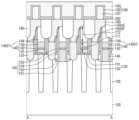
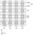
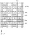
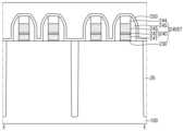
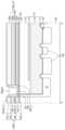
도 1은 몇몇 실시예들에 따른 반도체 메모리 장치의 셀 영역을 나타내는 개략적인 레이아웃이다.
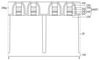
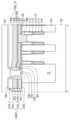
도 2는 도 1의 셀 영역을 포함하는 반도체 메모리 장치의 개략적인 레이아웃이다.
도 3의 도 1의 워드 라인 및 활성 영역만을 나타낸 레이아웃이다.
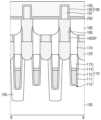
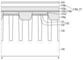
도 4 및 도 5는 각각 도 1의 A - A 및 B - B를 따라 절단한 단면도이다.
도 6 및 도 7은 각각 도 2의 C - C 및 D -D를 따라 절단한 단면도이다.
도 8은 도 2의 E - E를 따라 절단한 단면도이다.
도 9는 몇몇 실시예들에 따른 반도체 메모리 장치를 설명하기 위한 도면이다.
도 10은 몇몇 실시예들에 따른 반도체 메모리 장치를 설명하기 위한 도면이다.
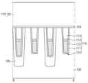
도 11은 몇몇 실시예들에 따른 반도체 메모리 장치를 설명하기 위한 레이아웃도이다.
도 12는 몇몇 실시예들에 따른 반도체 메모리 장치를 설명하기 위한 사시도이다.
도 13은 도 11의 F - F 및 G - G를 따라 절단한 단면도이다.
도 14는 몇몇 실시예들에 따른 반도체 메모리 장치를 설명하기 위한 레이아웃도이다.
도 15는 몇몇 실시예들에 따른 반도체 메모리 장치를 설명하기 위한 사시도이다.
도 16a 내지 도 21b는 몇몇 실시예들에 따른 반도체 메모리 장치 제조 방법을 설명하기 위한 중간단계 도면들이다.FIG. 1 is a schematic layout showing a cell region of a semiconductor memory device according to some embodiments.
FIG. 2 is a schematic layout of a semiconductor memory device including the cell region of FIG. 1.
FIG. 3 is a layout showing only the word lines and active areas of FIG. 1.
Figures 4 and 5 are cross-sectional views taken along lines A-A and B-B of Figure 1, respectively.
Figures 6 and 7 are cross-sectional views taken along lines C-C and D-D of Figure 2, respectively.
Figure 8 is a cross-sectional view taken along line E-E of Figure 2.
FIG. 9 is a drawing for explaining a semiconductor memory device according to some embodiments.
FIG. 10 is a drawing for explaining a semiconductor memory device according to some embodiments.
FIG. 11 is a layout diagram illustrating a semiconductor memory device according to some embodiments.
FIG. 12 is a perspective view illustrating a semiconductor memory device according to some embodiments.
Fig. 13 is a cross-sectional view taken along lines F-F and G-G of Fig. 11.
FIG. 14 is a layout diagram illustrating a semiconductor memory device according to some embodiments.
FIG. 15 is a perspective view illustrating a semiconductor memory device according to some embodiments.
FIGS. 16A to 21B are intermediate step drawings for explaining a method of manufacturing a semiconductor memory device according to some embodiments.
도 1은 몇몇 실시예들에 따른 반도체 메모리 장치의 셀 영역을 나타내는 개략적인 레이아웃이다. 도 2는 도 1의 셀 영역을 포함하는 반도체 메모리 장치의 개략적인 레이아웃이다. 도 3의 도 1의 워드 라인 및 활성 영역만을 나타낸 레이아웃이다. 도 4 및 도 5는 각각 도 1의 A - A 및 B - B를 따라 절단한 단면도이다. 도 6 및 도 7은 각각 도 2의 C - C 및 D -D를 따라 절단한 단면도이다. 도 8은 도 2의 E - E를 따라 절단한 단면도이다.FIG. 1 is a schematic layout showing a cell region of a semiconductor memory device according to some embodiments. FIG. 2 is a schematic layout of a semiconductor memory device including the cell region of FIG. 1. FIG. 3 is a layout showing only the word line and active region of FIG. 1. FIGS. 4 and 5 are cross-sectional views taken along lines A-A and B-B of FIG. 1, respectively. FIGS. 6 and 7 are cross-sectional views taken along lines C-C and D-D of FIG. 2, respectively. FIG. 8 is a cross-sectional view taken along line E-E of FIG.
참고적으로, 도 6는 셀 영역 분리막(22)에서 도 1의 비트 라인(BL)을 따라 절단한 단면도일 수 있다. 도 7은 셀 영역 분리막(22)에서 도 1의 워드 라인(WL)을 따라 절단한 단면도일 수 있다. 도 8은 페리(peri) 영역의 트랜지스터 형성 영역을 절단한 예시적인 단면도일 수 있다.For reference, FIG. 6 may be a cross-sectional view taken along the bit line (BL) of FIG. 1 in the cell area separator (22). FIG. 7 may be a cross-sectional view taken along the word line (WL) of FIG. 1 in the cell area separator (22). FIG. 8 may be an exemplary cross-sectional view taken along the transistor formation area of the peri area.
몇몇 실시예들에 따른 반도체 장치에 관한 도면에서, 예시적으로 DRAM(Dynamic Random Access Memory)이 도시되었지만, 이에 제한되는 것은 아니다.In the drawings relating to a semiconductor device according to some embodiments, a dynamic random access memory (DRAM) is illustrated as an example, but is not limited thereto.
도 1 내지 도 3을 참조하면, 몇몇 실시예들에 따른 반도체 장치는 셀 영역(20)과, 셀 영역 분리막(22)과, 페리 영역(24)을 포함할 수 있다.Referring to FIGS. 1 to 3, a semiconductor device according to some embodiments may include a cell region (20), a cell region separator (22), and a peripheral region (24).
셀 영역 분리막(22)은 셀 영역(20)의 둘레를 따라 형성될 수 있다. 셀 영역 분리막(22)은 셀 영역(20) 및 페리 영역(24)을 분리할 수 있다. 페리 영역(24)은 셀 영역(20)의 주변에 정의될 수 있다.A cell region separator (22) may be formed along the perimeter of the cell region (20). The cell region separator (22) may separate the cell region (20) and the peripheral region (24). The peripheral region (24) may be defined around the cell region (20).
셀 영역(20)은 복수의 셀 활성 영역(ACT)을 포함할 수 있다. 셀 활성 영역(ACT)은 기판(도 4의 100) 내에 형성된 셀 소자 분리막(도 4의 105)에 의해 정의될 수 있다. 반도체 장치의 디자인 룰의 감소에 따라, 도시된 바와 같이 셀 활성 영역(ACT)은 사선(diagonal line or oblique line)의 바(bar) 형태로 배치될 수 있다. 예를 들어, 셀 활성 영역(ACT)은 제3 방향(D3)으로 연장될 수 있다.The cell region (20) may include a plurality of cell active regions (ACTs). The cell active regions (ACTs) may be defined by a cell element isolation film (105 in FIG. 4) formed within a substrate (100 in FIG. 4). As the design rule of the semiconductor device is reduced, the cell active regions (ACTs) may be arranged in a bar shape of a diagonal line or an oblique line, as illustrated. For example, the cell active regions (ACTs) may extend in a third direction (D3).
셀 활성 영역(ACT)을 가로질러 제1 방향(D1)으로 복수의 게이트 전극이 배치될 수 있다. 복수의 게이트 전극은 서로 간에 평행하게 연장될 수 있다. 복수의 게이트 전극은 예를 들어, 복수의 워드 라인(Word Line: WL)일 수 있다. 워드 라인(WL)은 등 간격으로 배치될 수 있다. 워드 라인(WL)의 폭이나 워드 라인(WL) 사이의 간격은 디자인 룰에 따라 결정될 수 있다.A plurality of gate electrodes may be arranged in a first direction (D1) across a cell active area (ACT). The plurality of gate electrodes may extend parallel to one another. The plurality of gate electrodes may be, for example, a plurality of word lines (WL). The word lines (WL) may be arranged at equal intervals. The width of the word lines (WL) or the interval between the word lines (WL) may be determined according to a design rule.
제1 방향(D1)으로 연장되는 2개의 워드 라인(WL)에 의해, 각각의 셀 활성 영역(ACT)은 3 부분으로 나뉠 수 있다. 셀 활성 영역(ACT)은 스토리지 연결 영역(103b) 및 비트 라인 연결 영역(103a)을 포함할 수 있다. 비트 라인 연결 영역(103a)는 셀 활성 영역(ACT)의 가운데 부분에 위치하고, 스토리지 연결 영역(103b)는 셀 활성 영역(ACT)의 단부에 위치할 수 있다.Each cell active area (ACT) can be divided into three parts by two word lines (WL) extending in the first direction (D1). The cell active area (ACT) can include a storage connection area (103b) and a bit line connection area (103a). The bit line connection area (103a) can be located at a center portion of the cell active area (ACT), and the storage connection area (103b) can be located at an end portion of the cell active area (ACT).
워드 라인(WL) 상에는 워드 라인(WL)과 직교하는 제2 방향(D2)으로 연장되는 복수의 비트 라인(Bit Line: BL)이 배치될 수 있다. 복수의 비트 라인(BL)은 서로 간에 평행하게 연장될 수 있다. 비트 라인(BL)은 등 간격으로 배치될 수 있다. 비트 라인(BL)의 폭이나 비트 라인(BL) 사이의 간격은 디자인 룰에 따라 결정될 수 있다.A plurality of bit lines (Bit Lines: BL) extending in a second direction (D2) orthogonal to the word line (WL) may be arranged on the word line (WL). The plurality of bit lines (BL) may extend parallel to each other. The bit lines (BL) may be arranged at equal intervals. The width of the bit lines (BL) or the interval between the bit lines (BL) may be determined according to a design rule.
몇몇 실시예들에 따른 반도체 장치는 셀 활성 영역(ACT) 상에 형성된 다양한 컨택 배열들을 포함할 수 있다. 다양한 컨택 배열은 예를 들어, 다이렉트 컨택(Direct Contact: DC), 매몰 컨택(Buried Contact: BC), 및 랜딩 패드(Landing Pad: LP) 등을 포함할 수 있다.A semiconductor device according to some embodiments may include various contact arrangements formed on a cell active region (ACT). The various contact arrangements may include, for example, direct contacts (DC), buried contacts (BC), and landing pads (LP).
여기서, 다이렉트 컨택(DC)은 셀 활성 영역(ACT)을 비트 라인(BL)에 전기적으로 연결시키는 컨택을 의미할 수 있다. 매몰 컨택(BC)은 셀 활성 영역(ACT)을 커패시터의 하부 전극(도 4의 191)에 연결시키는 컨택을 의미할 수 있다. 배치 구조상, 매몰 컨택(BC)과 셀 활성 영역(ACT)의 접촉 면적이 작을 수 있다. 그에 따라, 셀 활성 영역(ACT)과 접촉 면적을 확대하는 것과 함께 커패시터의 하부 전극(도 4의 191)과의 접촉 면적 확대를 위해, 도전성의 랜딩 패드(LP)가 도입될 수 있다.Here, the direct contact (DC) may mean a contact that electrically connects the cell active region (ACT) to the bit line (BL). The buried contact (BC) may mean a contact that connects the cell active region (ACT) to the lower electrode (191 of FIG. 4) of the capacitor. Due to the arrangement structure, the contact area between the buried contact (BC) and the cell active region (ACT) may be small. Accordingly, a conductive landing pad (LP) may be introduced to expand the contact area with the cell active region (ACT) and the lower electrode (191 of FIG. 4) of the capacitor.
랜딩 패드(LP)는 셀 활성 영역(ACT)과 매몰 컨택(BC) 사이에 배치될 수도 있고, 매몰 컨택(BC)과 커패시터의 하부 전극(도 4의 191) 사이에 배치될 수도 있다. 몇몇 실시예들에 따른 반도체 장치에서, 랜딩 패드(LP)는 매몰 컨택(BC)과 커패시터의 하부 전극 사이에 배치될 수 있다. 랜딩 패드(LP)의 도입을 통해 접촉 면적을 확대함으로써, 셀 활성 영역(ACT)과 커패시터 하부 전극 사이의 컨택 저항이 감소될 수 있다.The landing pad (LP) may be disposed between the cell active region (ACT) and the buried contact (BC), or may be disposed between the buried contact (BC) and the lower electrode of the capacitor (191 in FIG. 4). In a semiconductor device according to some embodiments, the landing pad (LP) may be disposed between the buried contact (BC) and the lower electrode of the capacitor. By expanding the contact area through the introduction of the landing pad (LP), the contact resistance between the cell active region (ACT) and the lower electrode of the capacitor may be reduced.
다이렉트 컨택(DC)은 비트 라인 연결 영역(103a)과 연결될 수 있다. 매몰 컨택(BC)은 스토리지 연결 영역(103b)과 연결될 수 있다. 매몰 컨택(BC)이 셀 활성 영역(ACT)의 양 끝단 부분으로 배치됨에 따라, 랜딩 패드(LP)는 셀 활성 영역(ACT)의 양 끝단에 인접하여 매몰 콘택(BC)과 일부 오버랩되게 배치될 수 있다. 다르게 설명하면, 매몰 컨택(BC)은 인접하는 워드 라인(WL) 사이와, 인접하는 비트 라인(BL) 사이에 있는 셀 활성 영역(ACT) 및 셀 소자 분리막(도 4의 105)과 중첩되도록 형성될 수 있다.The direct contact (DC) may be connected to the bit line connection region (103a). The buried contact (BC) may be connected to the storage connection region (103b). As the buried contact (BC) is arranged at both ends of the cell active region (ACT), the landing pad (LP) may be arranged adjacent to both ends of the cell active region (ACT) to partially overlap with the buried contact (BC). In other words, the buried contact (BC) may be formed to overlap with the cell active region (ACT) and the cell device isolation film (105 in FIG. 4) between adjacent word lines (WL) and between adjacent bit lines (BL).
워드 라인(WL)은 기판(100) 내에 매몰된 구조로 형성될 수 있다. 워드 라인(WL)은 다이렉트 컨택(DC)이나 매몰 컨택(BC) 사이의 셀 활성 영역(ACT)을 가로질러 배치될 수 있다. 도시된 것과 같이, 2개의 워드 라인(WL)이 하나의 셀 활성 영역(ACT)을 가로지르도록 배치될 수 있다. 셀 활성 영역(ACT)이 제3 방향(D3)을 따라 연장됨으로써, 워드 라인(WL)은 셀 활성 영역(ACT)과 90도 미만의 각도를 가질 수 있다.The word line (WL) may be formed as a buried structure within the substrate (100). The word line (WL) may be arranged across the cell active area (ACT) between the direct contact (DC) or the buried contact (BC). As illustrated, two word lines (WL) may be arranged to cross one cell active area (ACT). Since the cell active area (ACT) extends along the third direction (D3), the word line (WL) may have an angle of less than 90 degrees with the cell active area (ACT).
다이렉트 컨택(DC) 및 매몰 컨택(BC)은 대칭적으로 배치될 수 있다. 이로 인해, 다이렉트 컨택(DC) 및 매몰 컨택(BC)은 제1 방향(D1) 및 제2 방향(D2)를 따라 일 직선 상에 배치될 수 있다. 한편, 다이렉트 컨택(DC) 및 매몰 컨택(BC)과 달리, 랜딩 패드(LP)는 비트 라인(BL)이 연장하는 제2 방향(D2)으로 지그재그 형태로 배치될 수 있다. 또한, 랜딩 패드(LP)는 워드 라인(WL)이 연장하는 제1 방향(D1)으로는 각 비트 라인(BL)의 동일한 측면 부분과 오버랩되게 배치될 수 있다. 예를 들어, 첫 번째 라인의 랜딩 패드(LP) 각각은 대응하는 비트 라인(BL)의 왼쪽 측면과 오버랩되고, 두 번째 라인의 랜딩 패드(LP) 각각은 대응하는 비트 라인(BL)의 오른쪽 측면과 오버랩될 수 있다.The direct contact (DC) and the buried contact (BC) can be arranged symmetrically. Therefore, the direct contact (DC) and the buried contact (BC) can be arranged on a straight line along the first direction (D1) and the second direction (D2). Meanwhile, unlike the direct contact (DC) and the buried contact (BC), the landing pads (LP) can be arranged in a zigzag shape in the second direction (D2) in which the bit line (BL) extends. In addition, the landing pads (LP) can be arranged to overlap with the same side portion of each bit line (BL) in the first direction (D1) in which the word line (WL) extends. For example, each landing pad (LP) of the first line can overlap with the left side of the corresponding bit line (BL), and each landing pad (LP) of the second line can overlap with the right side of the corresponding bit line (BL).
도 1 내지 도 8을 참고하면 몇몇 실시예들에 따른 반도체 장치는 복수의 셀 게이트 구조체(110)와, 복수의 비트 라인 구조체(140ST)와, 복수의 스토리지 컨택(120)과, 정보 저장부(190)와, 페리 게이트 구조체(240ST)를 포함할 수 있다.Referring to FIGS. 1 to 8, a semiconductor device according to some embodiments may include a plurality of cell gate structures (110), a plurality of bit line structures (140ST), a plurality of storage contacts (120), an information storage unit (190), and a peripheral gate structure (240ST).
기판(100)은 셀 영역(20)과, 셀 영역 분리막(22)과, 페리 영역(24)을 포함할 수 있다. 기판(100)은 실리콘 기판 또는 SOI(silicon-on-insulator)일 수 있다. 이와 달리, 기판(100)은 실리콘게르마늄, SGOI(silicon germanium on insulator), 안티몬화 인듐, 납 텔루르 화합물, 인듐 비소, 인듐 인화물, 갈륨 비소 또는 안티몬화 갈륨을 포함할 수 있으나, 이에 한정되는 것은 아니다.The substrate (100) may include a cell region (20), a cell region separator (22), and a peripheral region (24). The substrate (100) may be a silicon substrate or a silicon-on-insulator (SOI). Alternatively, the substrate (100) may include, but is not limited to, silicon germanium, silicon germanium on insulator (SGOI), indium antimonide, lead tellurium compound, indium arsenide, indium phosphide, gallium arsenide, or gallium antimonide.
복수의 셀 게이트 구조체(110)와, 복수의 비트 라인 구조체(140ST)와, 복수의 스토리지 컨택(120)과, 정보 저장부(190)는 셀 영역(20)에 배치될 수 있다. 페리 게이트 구조체(240ST)는 페리 영역(24)에 배치될 수 있다.A plurality of cell gate structures (110), a plurality of bit line structures (140ST), a plurality of storage contacts (120), and an information storage unit (190) may be arranged in a cell region (20). A peripheral gate structure (240ST) may be arranged in a peripheral region (24).
셀 소자 분리막(105)은 셀 영역(20)의 기판(100) 내에 형성될 수 있다. 셀 소자 분리막(105)은 우수한 소자 분리 특성을 갖는 STI(shallow trench isolation) 구조를 가질 수 있다. 셀 소자 분리막(105)은 셀 영역(20) 내에 셀 활성 영역(ACT)을 정의할 수 있다. 셀 소자 분리막(105)에 의해 정의된 셀 활성 영역(ACT)는 도 1에서 도시된 것과 같이 단축과 장축을 포함하는 긴 아일랜드 형성을 가질 수 있다. 셀 활성 영역(ACT)은 셀 소자 분리막(105) 내에 형성되는 워드 라인(WL)에 대하여 90도 미만의 각도를 갖도록 사선 형태를 가질 수 있다. 또한, 셀 활성 영역(ACT)는 셀 소자 분리막(105) 상에 형성되는 비트 라인(BL)에 대하여 90도 미만의 각도를 갖도록 사선 형태를 가질 수 있다.A cell device isolation film (105) may be formed within a substrate (100) of a cell region (20). The cell device isolation film (105) may have a shallow trench isolation (STI) structure having excellent device isolation characteristics. The cell device isolation film (105) may define a cell active region (ACT) within the cell region (20). The cell active region (ACT) defined by the cell device isolation film (105) may have a long island formation including a short axis and a long axis as illustrated in FIG. 1. The cell active region (ACT) may have an oblique shape so as to have an angle of less than 90 degrees with respect to a word line (WL) formed within the cell device isolation film (105). In addition, the cell active region (ACT) may have an oblique shape so as to have an angle of less than 90 degrees with respect to a bit line (BL) formed on the cell device isolation film (105).
셀 영역 분리막(22)도 STI 구조를 갖는 셀 경계 분리막이 형성될 수 있다. 셀 영역(20)은 셀 영역 분리막(22)에 의해 정의될 수 있다.A cell area separator (22) can also be formed as a cell boundary separator having an STI structure. The cell area (20) can be defined by the cell area separator (22).
셀 소자 분리막(105) 및 셀 영역 분리막(22)은 각각 예를 들어, 실리콘 산화막, 실리콘 질화막 및 실리콘 산질화막 중 적어도 하나를 포함할 수 있지만, 이에 제한되는 것은 아니다. 도 4 내지 도 8에서, 셀 소자 분리막(105) 및 셀 영역 분리막(22)은 각각 하나의 절연막으로 형성되는 것으로 도시되었지만, 설명의 편의를 위한 것일 뿐, 이에 제한되는 것은 아니다. 셀 소자 분리막(105) 및 셀 영역 분리막(22)의 폭에 따라, 셀 소자 분리막(105) 및 셀 영역 분리막(22)은 각각 하나의 절연막으로 형성될 수도 있고, 복수의 절연막으로 형성될 수도 있다.The cell element separator (105) and the cell region separator (22) may each include, for example, at least one of a silicon oxide film, a silicon nitride film, and a silicon oxynitride film, but are not limited thereto. In FIGS. 4 to 8, the cell element separator (105) and the cell region separator (22) are each illustrated as being formed of one insulating film, but this is only for convenience of explanation and is not limited thereto. Depending on the widths of the cell element separator (105) and the cell region separator (22), the cell element separator (105) and the cell region separator (22) may each be formed of one insulating film or may be formed of a plurality of insulating films.
도 6 및 도 7에서, 셀 소자 분리막(105)의 상면과, 기판(100)의 상면과, 셀 영역 분리막(22)의 상면은 동일 평면 상에 놓이는 것으로 도시하였지만, 설명의 편의를 위한 것일 뿐, 이에 제한되는 것은 아니다.In FIGS. 6 and 7, the upper surface of the cell element separator (105), the upper surface of the substrate (100), and the upper surface of the cell area separator (22) are depicted as being placed on the same plane, but this is only for convenience of explanation and is not limited thereto.
셀 게이트 구조체(110)는 기판(100) 및 셀 소자 분리막(105) 내에 형성될 수 있다. 게이트 구조체(110)는 셀 소자 분리막(105) 및 셀 소자 분리막(105)에 의해 정의된 셀 활성 영역(ACT)를 가로질러 형성될 수 있다. 셀 게이트 구조체(110)는 기판(100) 및 셀 소자 분리막(105) 내에 형성된 셀 게이트 트렌치(115)와, 셀 게이트 절연막(111)과, 셀 게이트 전극(112)과, 셀 게이트 캡핑 패턴(113)과, 셀 게이트 캡핑 도전막(114)을 포함할 수 있다. 여기에서, 셀 게이트 전극(112)은 워드 라인(WL)에 대응될 수 있다. 도시된 것과 달리, 셀 게이트 구조체(110)는 셀 게이트 캡핑 도전막(114)을 포함하지 않을 수 있다.A cell gate structure (110) may be formed within a substrate (100) and a cell device isolation film (105). The gate structure (110) may be formed across a cell active region (ACT) defined by the cell device isolation film (105) and the cell device isolation film (105). The cell gate structure (110) may include a cell gate trench (115) formed within the substrate (100) and the cell device isolation film (105), a cell gate insulating film (111), a cell gate electrode (112), a cell gate capping pattern (113), and a cell gate capping conductive film (114). Here, the cell gate electrode (112) may correspond to a word line (WL). Unlike what is illustrated, the cell gate structure (110) may not include the cell gate capping conductive film (114).
셀 게이트 절연막(111)은 셀 게이트 트렌치(115)의 측벽 및 바닥면을 따라 연장될 수 있다. 셀 게이트 절연막(111)은 셀 게이트 트렌치(115)의 적어도 일부의 프로파일을 따라 연장될 수 있다. 셀 게이트 절연막(111)은 예를 들어, 실리콘 산화물, 실리콘 질화물, 실리콘 산질화물, 또는 실리콘 산화물보다 높은 유전 상수를 갖는 고유전율 물질 중 적어도 하나를 포함할 수 있다. 고유전율 물질은 예를 들어, 하프늄 산화물(hafnium oxide), 하프늄 실리콘 산화물(hafnium silicon oxide), 하프늄 알루미늄 산화물(hafnium aluminum oxide), 란타늄 산화물(lanthanum oxide), 란타늄 알루미늄 산화물(lanthanum aluminum oxide), 지르코늄 산화물(zirconium oxide), 지르코늄 실리콘 산화물(zirconium silicon oxide), 탄탈륨 산화물(tantalum oxide), 티타늄 산화물(titanium oxide), 바륨 스트론튬 티타늄 산화물(barium strontium titanium oxide), 바륨 티타늄 산화물(barium titanium oxide), 스트론튬 티타늄 산화물(strontium titanium oxide), 이트륨 산화물(yttrium oxide), 알루미늄 산화물(aluminum oxide), 납 스칸듐 탄탈륨 산화물(lead scandium tantalum oxide), 납 아연 니오브산염(lead zinc niobate) 및 이들의 조합 중에서 적어도 하나를 포함할 수 있다.The cell gate insulating film (111) may extend along the sidewalls and bottom surface of the cell gate trench (115). The cell gate insulating film (111) may extend along the profile of at least a portion of the cell gate trench (115). The cell gate insulating film (111) may include at least one of, for example, silicon oxide, silicon nitride, silicon oxynitride, or a high-k material having a higher dielectric constant than silicon oxide. The high dielectric constant material can include at least one of, for example, hafnium oxide, hafnium silicon oxide, hafnium aluminum oxide, lanthanum oxide, lanthanum aluminum oxide, zirconium oxide, zirconium silicon oxide, tantalum oxide, titanium oxide, barium strontium titanium oxide, barium titanium oxide, strontium titanium oxide, yttrium oxide, aluminum oxide, lead scandium tantalum oxide, lead zinc niobate, and combinations thereof.
셀 게이트 전극(112)은 셀 게이트 절연막(111) 상에 형성될 수 있다. 셀 게이트 전극(112)은 셀 게이트 트렌치(115)의 일부를 채울 수 있다. 셀 게이트 캡핑 도전막(114)은 셀 게이트 전극(112)의 상면을 따라 연장될 수 있다. 도 7에서, 셀 게이트 캡핑 도전막(114)은 셀 게이트 전극(112)의 상면의 일부를 덮지 않는 것으로 도시하였지만, 이에 제한되는 것은 아니다.The cell gate electrode (112) may be formed on the cell gate insulating film (111). The cell gate electrode (112) may fill a portion of the cell gate trench (115). The cell gate capping conductive film (114) may extend along the upper surface of the cell gate electrode (112). In FIG. 7, the cell gate capping conductive film (114) is illustrated as not covering a portion of the upper surface of the cell gate electrode (112), but is not limited thereto.
셀 게이트 전극(112)은 금속, 금속 합금, 도전성 금속 질화물, 도전성 금속 탄질화물, 도전성 금속 탄화물, 금속 실리사이드, 도핑된 반도체 물질, 도전성 금속 산질화물 및 도전성 금속 산화물 중 적어도 하나를 포함할 수 있다. 셀 게이트 전극(112)는 예를 들어, TiN, TaC, TaN, TiSiN, TaSiN, TaTiN, TiAlN, TaAlN, WN, Ru, TiAl, TiAlC-N, TiAlC, TiC, TaCN, W, Al, Cu, Co, Ti, Ta, Ni, Pt, Ni-Pt, Nb, NbN, NbC, Mo, MoN, MoC, WC, Rh, Pd, Ir, Ag, Au, Zn, V, RuTiN, TiSi, TaSi, NiSi, CoSi, IrOx, RuOx 및 이들의 조합 중 적어도 하나를 포함할 수 있지만, 이에 제한되는 것은 아니다. 셀 게이트 캡핑 도전막(114)은 예를 들어, 폴리 실리콘 또는 폴리 실리콘 게르마늄을 포함할 수 있지만, 이에 제한되는 것은 아니다.The cell gate electrode (112) may include at least one of a metal, a metal alloy, a conductive metal nitride, a conductive metal carbonitride, a conductive metal carbide, a metal silicide, a doped semiconductor material, a conductive metal oxynitride, and a conductive metal oxide. The cell gate electrode (112) may include at least one of, but is not limited to, TiN, TaC, TaN, TiSiN, TaSiN, TaTiN, TiAlN, TaAlN, WN, Ru, TiAl, TiAlC-N, TiAlC, TiC, TaCN, W, Al, Cu, Co, Ti, Ta, Ni, Pt, Ni-Pt, Nb, NbN, NbC, Mo, MoN, MoC, WC, Rh, Pd, Ir, Ag, Au, Zn, V, RuTiN, TiSi, TaSi, NiSi, CoSi, IrOx, RuOx, and combinations thereof. The cell gate capping conductive film (114) may include, but is not limited to, polysilicon or polysilicon germanium, for example.
셀 게이트 캡핑 패턴(113)은 셀 게이트 전극(112) 및 셀 게이트 캡핑 도전막(114) 상에 배치될 수 있다. 셀 게이트 캡핑 패턴(113)은 셀 게이트 전극(112) 및 셀 게이트 캡핑 도전막(114)이 형성되고 남은 셀 게이트 트렌치(115)를 채울 수 있다. 셀 게이트 절연막(111)은 셀 게이트 캡핑 패턴(113)의 측벽을 따라 연장되는 것으로 도시하였지만, 이에 제한되는 것은 아니다. 셀 게이트 캡핑 패턴(113)은 예를 들어, 실리콘 질화물(SiN), 실리콘 산질화물(SiON), 실리콘 산화물(SiO2), 실리콘 탄질화물(SiCN), 실리콘 산탄질화물(SiOCN) 및 이들의 조합 중 적어도 하나를 포함할 수 있다.The cell gate capping pattern (113) may be disposed on the cell gate electrode (112) and the cell gate capping conductive film (114). The cell gate capping pattern (113) may fill the cell gate trench (115) remaining after the cell gate electrode (112) and the cell gate capping conductive film (114) are formed. The cell gate insulating film (111) is illustrated as extending along the sidewall of the cell gate capping pattern (113), but is not limited thereto. The cell gate capping pattern (113) may include, for example, at least one of silicon nitride (SiN), silicon oxynitride (SiON), silicon oxide (SiO2 ), silicon carbon nitride (SiCN), silicon oxycarbon nitride (SiOCN), and combinations thereof.
도시되지 않았지만, 셀 게이트 구조체(110)의 적어도 일측에는 불순물 도핑 영역이 형성될 수 있다. 불순물 도핑 영역은 트랜지스터의 소오스/드레인 영역일 수 있다.Although not shown, an impurity doped region may be formed on at least one side of the cell gate structure (110). The impurity doped region may be a source/drain region of the transistor.
비트 라인 구조체(140ST)는 셀 도전 라인(140)과, 셀 라인 캡핑막(144)을 포함할 수 있다. 셀 도전 라인(140)은 셀 게이트 구조체(110)가 형성된 기판(100) 및 셀 소자 분리막(105) 상에 형성될 수 있다. 셀 도전 라인(140)은 셀 소자 분리막(105) 및 셀 소자 분리막(105)에 의해 정의된 셀 활성 영역(ACT)과 교차할 수 있다. 셀 도전 라인(140)은 셀 게이트 구조체(110)와 교차되도록 형성될 수 있다. 여기에서, 셀 도전 라인(140)은 비트 라인(BL)에 대응될 수 있다.The bit line structure (140ST) may include a cell conductive line (140) and a cell line capping film (144). The cell conductive line (140) may be formed on a substrate (100) on which a cell gate structure (110) is formed and a cell element isolation film (105). The cell conductive line (140) may intersect the cell element isolation film (105) and a cell active region (ACT) defined by the cell element isolation film (105). The cell conductive line (140) may be formed to intersect the cell gate structure (110). Here, the cell conductive line (140) may correspond to a bit line (BL).
셀 도전 라인(140)은 다중막일 수 있다. 셀 도전 라인(140)은 예를 들어, 제1 셀 도전막(141)과, 제2 셀 도전막(142)과, 제3 셀 도전막(143)을 포함할 수 있다. 제1 내지 제3 셀 도전막(141, 142, 143)은 기판(100) 및 셀 소자 분리막(105) 상에 순차적으로 적층될 수 있다. 셀 도전 라인(140)이 3중막인 것으로 도시되었지만, 이에 제한되는 것은 아니다.The cell conductive line (140) may be a multilayer. The cell conductive line (140) may include, for example, a first cell conductive film (141), a second cell conductive film (142), and a third cell conductive film (143). The first to third cell conductive films (141, 142, 143) may be sequentially laminated on the substrate (100) and the cell element isolation film (105). Although the cell conductive line (140) is illustrated as a triple layer, it is not limited thereto.
제1 내지 제3 셀 도전막(141, 142, 143)은 각각 예를 들어, 불순물이 도핑된 반도체 물질, 도전성 실리사이드 화합물, 도전성 금속 질화물 금속 및 금속 합금 중 적어도 하나를 포함할 수 있다. 예를 들어, 제1 셀 도전막(141)은 도핑된 반도체 물질을 포함하고, 제2 셀 도전막(142)은 도전성 실리사이드 화합물 및 도전성 금속 질화물 중 적어도 하나를 포함하고, 제3 셀 도전막(143)은 금속 및 금속 합금 중 적어도 하나를 포함할 수 있지만, 이에 제한되는 것은 아니다.The first to third cell conductive films (141, 142, 143) may each include, for example, at least one of a doped semiconductor material, a conductive silicide compound, a conductive metal nitride, a metal, and a metal alloy. For example, the first cell conductive film (141) may include a doped semiconductor material, the second cell conductive film (142) may include at least one of a conductive silicide compound and a conductive metal nitride, and the third cell conductive film (143) may include at least one of a metal and a metal alloy, but is not limited thereto.
비트 라인 컨택(146)은 셀 도전 라인(140)과 기판(100) 사이에 형성될 수 있다. 즉, 셀 도전 라인(140)은 비트 라인 컨택(146) 상에 형성될 수 있다. 예를 들어, 비트 라인 컨택(146)은 셀 도전 라인(140)이 긴 아일랜드 형상을 갖는 셀 활성 영역(ACT)의 가운데 부분과 교차하는 지점에 형성될 수 있다. 비트 라인 컨택(146)은 비트 라인 연결 영역(103a)과 배선 구조체(140) 사이에 형성될 수 있다.The bit line contact (146) may be formed between the cell conductive line (140) and the substrate (100). That is, the cell conductive line (140) may be formed on the bit line contact (146). For example, the bit line contact (146) may be formed at a point where the cell conductive line (140) intersects the center portion of a cell active region (ACT) having a long island shape. The bit line contact (146) may be formed between the bit line connection region (103a) and the wiring structure (140).
비트 라인 컨택(146)은 셀 도전 라인(140)과 기판(100)을 전기적으로 연결할 수 있다. 여기에서, 비트 라인 컨택(146)은 다이렉트 컨택(DC)에 대응될 수 있다. 비트 라인 컨택(146)은 예를 들어, 불순물이 도핑된 반도체 물질, 도전성 실리사이드 화합물, 도전성 금속 질화물 및 금속 중 적어도 하나를 포함할 수 있다.The bit line contact (146) can electrically connect the cell conductive line (140) and the substrate (100). Here, the bit line contact (146) can correspond to a direct contact (DC). The bit line contact (146) can include, for example, at least one of a semiconductor material doped with an impurity, a conductive silicide compound, a conductive metal nitride, and a metal.
도 4에서, 비트 라인 컨택(146)의 상면과 중첩되는 영역에서, 셀 도전 라인(140)은 제2 셀 도전막(142) 및 제3 셀 도전막(143)을 포함할 수 있다. 비트 라인 컨택(146)의 상면과 중첩되는 않는 영역에서, 셀 도전 라인(140)은 제1 내지 제3 셀 도전막(141, 142, 143)을 포함할 수 있다.In FIG. 4, in an area overlapping with the upper surface of the bit line contact (146), the cell conductive line (140) may include a second cell conductive film (142) and a third cell conductive film (143). In an area not overlapping with the upper surface of the bit line contact (146), the cell conductive line (140) may include first to third cell conductive films (141, 142, 143).
셀 라인 캡핑막(144)은 셀 도전 라인(140) 상에 배치될 수 있다. 셀 라인 캡핑막(144)은 셀 도전 라인(140)의 상면을 따라 제2 방향(D2)으로 연장될 수 있다. 이 때, 셀 라인 캡핑막(144)은 예를 들어, 실리콘 질화막, 실리콘 산질화물, 실리콘 탄질화물 및 실리콘 산탄질화물 중 적어도 하나를 포함할 수 있다. 몇몇 실시예들에 따른 반도체 메모리 장치에서, 셀 라인 캡핑막(144)은 예를 들어, 실리콘 질화막을 포함할 수 있다. 셀 라인 캡핑막(144)은 단일막인 것으로 도시되었지만, 이에 제한되는 것은 아니다. 즉, 도 20a에 도시된 것과 같이, 셀 라인 캡핑막(144)은 다중막일 수도 있다. 다만, 다중막을 구성하는 각각의 막이 동일한 물질일 경우, 셀 라인 캡핑막(144)은 단일막으로 보여질 수도 있다.The cell line capping film (144) may be disposed on the cell conductive line (140). The cell line capping film (144) may extend in the second direction (D2) along the upper surface of the cell conductive line (140). At this time, the cell line capping film (144) may include, for example, at least one of a silicon nitride film, silicon oxynitride, silicon carbon nitride, and silicon oxycarbon nitride. In a semiconductor memory device according to some embodiments, the cell line capping film (144) may include, for example, a silicon nitride film. The cell line capping film (144) is illustrated as a single film, but is not limited thereto. That is, as illustrated in FIG. 20A, the cell line capping film (144) may be a multi-film. However, when each film constituting the multi-film is made of the same material, the cell line capping film (144) may be viewed as a single film.
셀 절연막(130)은 기판(100) 및 셀 소자 분리막(105) 상에 형성될 수 있다. 좀 더 구체적으로, 셀 절연막(130)은 비트 라인 컨택(146)이 형성되지 않은 기판(100) 및 셀 소자 분리막(105) 상에 형성될 수 있다. 셀 절연막(130)은 기판(100) 및 셀 도전 라인(140) 사이와, 셀 소자 분리막(105) 및 셀 도전 라인(140) 사이에 형성될 수 있다.The cell insulation film (130) may be formed on the substrate (100) and the cell element separation film (105). More specifically, the cell insulation film (130) may be formed on the substrate (100) and the cell element separation film (105) where the bit line contact (146) is not formed. The cell insulation film (130) may be formed between the substrate (100) and the cell conductive line (140), and between the cell element separation film (105) and the cell conductive line (140).
셀 절연막(130)은 단일막일 수 있으나, 도시된 것처럼, 셀 절연막(130)은 제1 셀 절연막(131) 및 제2 셀 절연막(132)을 포함하는 다중막일 수도 있다. 예를 들어, 제1 셀 절연막(131)은 실리콘 산화막을 포함할 수 있고, 제2 셀 절연막(132)은 실리콘 질화막을 포함할 수 있지만, 이에 제한되는 것은 아니다.The cell insulating film (130) may be a single film, but as illustrated, the cell insulating film (130) may also be a multi-film including a first cell insulating film (131) and a second cell insulating film (132). For example, the first cell insulating film (131) may include a silicon oxide film, and the second cell insulating film (132) may include a silicon nitride film, but is not limited thereto.
셀 버퍼막(101)은 셀 절연막(130)과 셀 영역 분리막(22) 사이에 배치될 수 있다. 셀 버퍼막(101)은 예를 들어, 실리콘 산화막을 포함할 수 있지만, 이에 제한되는 것은 아니다.A cell buffer film (101) may be placed between a cell insulating film (130) and a cell area separator film (22). The cell buffer film (101) may include, for example, a silicon oxide film, but is not limited thereto.
셀 라인 스페이서(150)는 셀 도전 라인(140) 및 셀 라인 캡핑막(144)의 측벽 상에 배치될 수 있다. 셀 라인 스페이서(150)는 비트 라인 컨택(146)이 형성된 셀 도전 라인(140)의 부분에서 기판(100) 및 셀 소자 분리막(105) 상에 형성될 수 있다. 셀 라인 스페이서(150)는 셀 도전 라인(140) 셀 라인 캡핑막(144) 및 비트 라인 컨택(146)의 측벽 상에서 배치될 수 있다.The cell line spacer (150) may be disposed on the sidewalls of the cell conductive line (140) and the cell line capping film (144). The cell line spacer (150) may be formed on the substrate (100) and the cell element isolation film (105) at a portion of the cell conductive line (140) where the bit line contact (146) is formed. The cell line spacer (150) may be disposed on the sidewalls of the cell conductive line (140), the cell line capping film (144), and the bit line contact (146).
그러나, 비트 라인 컨택(146)이 형성되지 않은 셀 도전 라인(140)의 나머지 부분에서, 셀 라인 스페이서(150)는 셀 절연막(130) 상에 배치될 수 있다. 셀 라인 스페이서(150)는 셀 도전 라인(140) 및 셀 라인 캡핑막(144)의 측벽 상에서 배치될 수 있다.However, in the remaining portion of the cell conductive line (140) where the bit line contact (146) is not formed, the cell line spacer (150) may be placed on the cell insulating film (130). The cell line spacer (150) may be placed on the sidewalls of the cell conductive line (140) and the cell line capping film (144).
셀 라인 스페이서(150)는 단일막일 수 있으나, 도시된 것처럼, 셀 라인 스페이서(150)는 제1 내지 제4 셀 라인 스페이서(151, 152, 153, 154)를 포함하는 다중막일 수도 있다. 예를 들어, 제1 내지 제4 셀 라인 스페이서(151, 152, 153, 154)는 실리콘 산화막, 실리콘 질화막, 실리콘 산질화막(SiON), 실리콘 산탄질화막(SiOCN), 에어(air) 및 이들의 조합을 하나를 포함할 수 있으나, 이에 제한되는 것은 아니다.The cell line spacer (150) may be a single film, but as illustrated, the cell line spacer (150) may also be a multi-film including first to fourth cell line spacers (151, 152, 153, 154). For example, the first to fourth cell line spacers (151, 152, 153, 154) may include, but are not limited to, a silicon oxide film, a silicon nitride film, a silicon oxynitride (SiON) film, a silicon carbonitride (SiOCN) film, air, and combinations thereof.
예를 들어, 제2 셀 라인 스페이서(152)는 셀 도전막(130) 상에 배치되지 않지만, 비트 라인 컨택(146)의 측벽 상에 배치될 수 있다. 도 7에서, 셀 게이트 구조체(110)의 상면 상에서, 제4 셀 라인 스페이서(154)는 제1 방향(D1)으로 인접하는 셀 도전 라인(140)의 측벽과, 셀 게이트 캡핑 패턴(113)의 상면을 따라 연장될 수 있다.For example, the second cell line spacer (152) may not be disposed on the cell conductive film (130), but may be disposed on the sidewall of the bit line contact (146). In FIG. 7, on the upper surface of the cell gate structure (110), the fourth cell line spacer (154) may extend along the sidewall of the adjacent cell conductive line (140) in the first direction (D1) and the upper surface of the cell gate capping pattern (113).
도 6에서, 비트 라인 구조체(140ST)는 제2 방향(D2)으로 길게 연장될 수 있다. 비트 라인 구조체(140ST)는 셀 영역 분리막(22) 상에 정의된 단측벽을 포함할 수 있다. 비트 라인 구조체(140ST)의 단측벽 상에, 제1 셀 경계 스페이서(246_1)가 배치될 수 있다.In FIG. 6, the bit line structure (140ST) may be extended in the second direction (D2). The bit line structure (140ST) may include a single-side wall defined on the cell area separator (22). A first cell boundary spacer (246_1) may be arranged on the single-side wall of the bit line structure (140ST).
즉, 셀 라인 스페이서(150)는 비트 라인 구조체(140ST)의 측벽 중 제2 방향(D2)으로 길게 연장된 장측벽 상에 배치될 수 있다.That is, the cell line spacer (150) can be placed on a long side wall extending in the second direction (D2) among the side walls of the bit line structure (140ST).
도 7에서, 더미 비트 라인 구조체(140ST_1)는 셀 영역 분리막(22) 상에 배치될 수 있다. 더미 비트 라인 구조체(140ST_1)는 비트 라인 구조체(140ST)와 동일한 구조를 가질 수 있다. 즉, 더미 비트 라인 구조체(140ST_1)는 셀 도전 라인(140)과, 셀 라인 캡핑막(144)을 포함할 수 있다.In FIG. 7, a dummy bit line structure (140ST_1) may be placed on a cell area separator (22). The dummy bit line structure (140ST_1) may have the same structure as the bit line structure (140ST). That is, the dummy bit line structure (140ST_1) may include a cell conductive line (140) and a cell line capping film (144).
비트 라인 구조체(140ST)와 마주보는 더미 비트 라인 구조체(140ST_1)의 제1 측벽 상에, 제1 셀 라인 스페이서(151) 및 제3 셀 라인 스페이서(153)이 형성될 수 있다. 더미 비트 라인 구조체(140ST_1)의 제1 측벽과 제1 방향(D1)으로 반대되는 제2 측벽 상에, 제2 셀 경계 스페이서(246_2)가 배치될 수 있다. 제2 셀 경계 스페이서(246_2)와 제1 셀 경계 스페이서(246_1)는 이 후에 설명되는 페리 스페이서(245), 제1 블록 스페이서(245_1) 및 제2 블록 스페이서(245_2)와 동일 레벨에서 형성될 수 있다. 여기서, "동일 레벨"이라 함은 동일한 제조 공정에 의해 형성되는 것을 의미하는 것이다.A first cell line spacer (151) and a third cell line spacer (153) may be formed on a first sidewall of a dummy bit line structure (140ST_1) facing a bit line structure (140ST). A second cell boundary spacer (246_2) may be arranged on a second sidewall opposite to the first sidewall of the dummy bit line structure (140ST_1) in the first direction (D1). The second cell boundary spacer (246_2) and the first cell boundary spacer (246_1) may be formed at the same level as the peripheral spacer (245), the first block spacer (245_1), and the second block spacer (245_2) described later. Here, “the same level” means that they are formed by the same manufacturing process.
펜스 패턴(170)은 기판(100) 및 셀 소자 분리막(105) 상에 배치될 수 있다. 펜스 패턴(170)은 기판(100) 및 셀 소자 분리막(105) 내에 형성된 셀 게이트 구조체(110)와 중첩되도록 형성될 수 있다. 펜스 패턴(170)은 제2 방향(D2)으로 연장되는 비트 라인 구조체(140ST) 사이에 배치될 수 있다. 펜스 패턴(170)은 예를 들어, 실리콘 산화물, 실리콘 질화물, 실리콘 산질화물 및 이들의 조합 중 적어도 하나를 포함할 수 있다.The fence pattern (170) may be arranged on the substrate (100) and the cell device isolation film (105). The fence pattern (170) may be formed to overlap with the cell gate structure (110) formed in the substrate (100) and the cell device isolation film (105). The fence pattern (170) may be arranged between the bit line structures (140ST) extending in the second direction (D2). The fence pattern (170) may include, for example, at least one of silicon oxide, silicon nitride, silicon oxynitride, and a combination thereof.
스토리지 컨택(120)은 제1 방향(D1)으로 인접하는 셀 도전 라인(140) 사이에 배치될 수 있다. 스토리지 컨택(120)은 제2 방향(D2)으로 인접하는 펜스 패턴(170) 사이에 배치될 수 있다. 스토리지 컨택(120)은 인접하는 셀 도전 라인(140) 사이의 기판(100) 및 셀 소자 분리막(105)과 중첩될 수 있다. 스토리지 컨택(120)은 셀 활성 영역(ACT)의 스토리지 연결 영역(103b)과 연결될 수 있다. 여기에서, 스토리지 컨택(120)은 매몰 컨택(BC)에 대응될 수 있다.The storage contact (120) may be arranged between adjacent cell conductive lines (140) in a first direction (D1). The storage contact (120) may be arranged between adjacent fence patterns (170) in a second direction (D2). The storage contact (120) may overlap the substrate (100) and the cell element isolation film (105) between the adjacent cell conductive lines (140). The storage contact (120) may be connected to the storage connection region (103b) of the cell active region (ACT). Here, the storage contact (120) may correspond to a buried contact (BC).
스토리지 컨택(120)은 예를 들어, 불순물이 도핑된 반도체 물질, 도전성 실리사이드 화합물, 도전성 금속 질화물 및 금속 중 적어도 하나를 포함할 수 있다.The storage contact (120) may include, for example, at least one of a semiconductor material doped with impurities, a conductive silicide compound, a conductive metal nitride, and a metal.
스토리지 패드(160) 스토리지 컨택(120) 상에 형성될 수 있다. 스토리지 패드(160)은 스토리지 컨택(120)과 전기적으로 연결될 수 있다. 여기에서, 스토리지 패드(160)는 랜딩 패드(LP)에 대응될 수 있다.A storage pad (160) may be formed on a storage contact (120). The storage pad (160) may be electrically connected to the storage contact (120). Here, the storage pad (160) may correspond to a landing pad (LP).
스토리지 패드(160)는 비트 라인 구조체(140ST)의 상면의 일부와 중첩될 수 있다. 스토리지 패드(160)는 예를 들어, 불순물이 도핑된 반도체 물질, 도전성 실리사이드 화합물, 도전성 금속 질화물, 도전성 금속 탄화물, 금속 및 금속 합금 중 적어도 하나를 포함할 수 있다.The storage pad (160) may overlap a portion of the upper surface of the bit line structure (140ST). The storage pad (160) may include, for example, at least one of a semiconductor material doped with an impurity, a conductive silicide compound, a conductive metal nitride, a conductive metal carbide, a metal, and a metal alloy.
스토리지 패드 스페이서(160SP)는 스토리지 컨택(120) 상에 배치될 수 있다. 스토리지 패드 스페이서(160SP)는 스토리지 패드(160)와 비트 라인 구조체(140ST) 사이와, 스토리지 패턴(160)과 펜스 패턴(170) 사이에 배치될 수 있다. 도시된 것과 달리, 스토리지 패드 스페이서(160SP)는 생략될 수 있다. 스토리지 패드 스페이서(160SP)는 예를 들어, 실리콘 산화막, 실리콘 질화막, 실리콘 산질화막, 실리콘 산탄질화막 및 실리콘 탄질화막(SiCN) 중 적어도 하나를 포함할 수 있다.A storage pad spacer (160SP) may be placed on a storage contact (120). The storage pad spacer (160SP) may be placed between a storage pad (160) and a bit line structure (140ST) and between a storage pattern (160) and a fence pattern (170). Unlike what is illustrated, the storage pad spacer (160SP) may be omitted. The storage pad spacer (160SP) may include, for example, at least one of a silicon oxide film, a silicon nitride film, a silicon oxynitride film, a silicon carbonitride film, and a silicon carbon nitride film (SiCN).
패드 분리 절연막(180)은 스토리지 패드(160) 및 비트 라인 구조체(140ST) 상에 형성될 수 있다. 예를 들어, 패드 분리 절연막(180)은 셀 라인 캡핑막(144) 상에 배치될 수 있다. 패드 분리 절연막(180)은 복수의 고립 영역을 형성하는 스토리지 패드(160)의 영역을 정의할 수 있다. 또한, 패드 분리 절연막(180)은 스토리지 패드(160)의 상면을 덮지 않을 수 있다.The pad separation insulating film (180) may be formed on the storage pad (160) and the bit line structure (140ST). For example, the pad separation insulating film (180) may be disposed on the cell line capping film (144). The pad separation insulating film (180) may define an area of the storage pad (160) forming a plurality of isolation areas. Additionally, the pad separation insulating film (180) may not cover an upper surface of the storage pad (160).
패드 분리 절연막(180)은 절연성 물질을 포함하여, 복수의 스토리지 패드(160)를 서로 전기적으로 분리할 수 있다. 예를 들어, 패드 분리 절연막(180)은 예를 들어, 실리콘 산화막, 실리콘 질화막, 실리콘 산질화막, 실리콘 산탄질화막 및 실리콘 탄질화막 중 적어도 하나를 포함할 수 있다.The pad separation insulating film (180) may include an insulating material to electrically isolate a plurality of storage pads (160) from each other. For example, the pad separation insulating film (180) may include at least one of a silicon oxide film, a silicon nitride film, a silicon oxynitride film, a silicon oxycarbonitride film, and a silicon carbonitride film.
제1 식각 정지막(292)는 패드 분리 절연막(180) 및 스토리지 패드(160) 상에 배치될 수 있다. 제1 식각 정지막(292)은 셀 영역(20)뿐만 아니라, 페리 영역(24)까지 연장될 수 있다. 제1 식각 정지막(292)는 실리콘 질화막, 실리콘 탄질화막, 실리콘 붕소질화막(SiBN), 실리콘 산질화막, 실리콘 산탄화막 중 적어도 하나를 포함할 수 있다.The first etching stop film (292) may be disposed on the pad separation insulating film (180) and the storage pad (160). The first etching stop film (292) may extend to the cell region (20) as well as the peripheral region (24). The first etching stop film (292) may include at least one of a silicon nitride film, a silicon carbonitride film, a silicon boron nitride (SiBN) film, a silicon oxynitride film, and a silicon oxycarbonate film.
정보 저장부(190)는 스토리지 패드(160) 상에 배치될 수 있다. 정보 저장부(190)는 스토리지 패드(160)와 전기적으로 연결될 수 있다. 정보 저장부(190)의 일부는 식각 정지막(292) 내에 배치될 수 있다. 정보 저장부(190)는 예를 들어, 커패시터를 포함할 수 있지만, 이에 제한되는 것은 아니다. 정보 저장부(190)는 제1 하부 전극(191)과, 제1 커패시터 유전막(192)과, 제1 상부 전극(193)을 포함한다.The information storage unit (190) may be placed on the storage pad (160). The information storage unit (190) may be electrically connected to the storage pad (160). A portion of the information storage unit (190) may be placed within the etch stop film (292). The information storage unit (190) may include, for example, a capacitor, but is not limited thereto. The information storage unit (190) includes a first lower electrode (191), a first capacitor dielectric film (192), and a first upper electrode (193).
제1 하부 전극(191)은 스토리지 패드(160) 상에 배치될 수 있다. 제1 하부 전극(191)은 필라 형상을 갖는 것으로 도시하였지만, 이에 제한되는 것은 아니다. 제1 하부 전극(191)은 실린더 형상을 가질 수 있음은 물론이다. 제1 커패시터 유전막(192)은 제1 하부 전극(191) 상에 형성된다. 제1 커패시터 유전막(192)은 제1 하부 전극(191)의 프로파일을 따라 형성될 수 있다. 제1 상부 전극(193)은 제1 커패시터 유전막(192) 상에 형성된다. 제1 상부 전극(193)은 제1 하부 전극(191)의 외측벽을 감쌀 수 있다.The first lower electrode (191) may be placed on the storage pad (160). The first lower electrode (191) is illustrated as having a pillar shape, but is not limited thereto. The first lower electrode (191) may of course have a cylindrical shape. The first capacitor dielectric film (192) is formed on the first lower electrode (191). The first capacitor dielectric film (192) may be formed along the profile of the first lower electrode (191). The first upper electrode (193) is formed on the first capacitor dielectric film (192). The first upper electrode (193) may surround an outer wall of the first lower electrode (191).
일 예로, 제1 커패시터 유전막(192)은 제1 상부 전극(193)과 수직으로 중첩되는 부분에 배치될 수 있다. 다른 예로, 도시된 것과 달리, 제1 커패시터 유전막(192)은 제1 상부 전극(193)과 수직으로 중첩되는 제1 부분과, 제1 상부 전극(193)과 수직으로 중첩되지 않는 제2 부분을 포함할 수 있다. 즉, 제1 커패시터 유전막(192)의 제2 부분은 제1 상부 전극(193)에 의해 덮이지 않는 부분이다.For example, the first capacitor dielectric film (192) may be positioned in a portion that vertically overlaps the first upper electrode (193). As another example, unlike what is illustrated, the first capacitor dielectric film (192) may include a first portion that vertically overlaps the first upper electrode (193) and a second portion that does not vertically overlap the first upper electrode (193). That is, the second portion of the first capacitor dielectric film (192) is a portion that is not covered by the first upper electrode (193).
제1 하부 전극(191) 및 제1 상부 전극(193)은 각각 예를 들어, 도핑된 반도체 물질, 도전성 금속 질화물(예를 들어, 티타늄 질화물, 탄탈륨 질화물, 나이오븀 질화물 또는 텅스텐 질화물 등), 금속(예를 들어, 루세늄, 이리듐, 티타늄 또는 탄탈륨 등), 및 도전성 금속 산화물(예를 들어, 이리듐 산화물 또는 나이오븀 산화물 등) 등을 포함할 수 있지만, 이에 제한되는 것은 아니다.The first lower electrode (191) and the first upper electrode (193) may each include, but are not limited to, for example, a doped semiconductor material, a conductive metal nitride (e.g., titanium nitride, tantalum nitride, niobium nitride, or tungsten nitride), a metal (e.g., ruthenium, iridium, titanium, or tantalum), and a conductive metal oxide (e.g., iridium oxide or niobium oxide).
제1 커패시터 유전막(192)은 예를 들어, 실리콘 산화물, 실리콘 질화물, 실리콘 산질화물 및 고유전율 물질 및 이들의 조합 중에서 하나를 포함할 수 있지만, 이에 제한되는 것은 아니다. 몇몇 실시예들에 따른 반도체 장치에서, 제1 커패시터 유전막(192)은 지르코늄 산화물(zirconium oxide), 알루미늄 산화물(aluminum oxide) 및 지르코늄 산화물(zirconium oxide)이 순차적으로 적층된 적층막 구조를 포함할 수 있다. 몇몇 실시예들에 따른 반도체 장치에서, 제1 커패시터 유전막(192)은 하프늄(Hf)을 포함하는 유전막을 포함할 수 있다. 몇몇 실시예들에 따른 반도체 장치에서, 제1 커패시터 유전막(192)은 강유전체 물질막과 상유전체 물질막의 적층막 구조를 가질 수 있다.The first capacitor dielectric film (192) may include, but is not limited to, one of, for example, silicon oxide, silicon nitride, silicon oxynitride, and a high-k material and a combination thereof. In a semiconductor device according to some embodiments, the first capacitor dielectric film (192) may include a laminated film structure in which zirconium oxide, aluminum oxide, and zirconium oxide are sequentially laminated. In a semiconductor device according to some embodiments, the first capacitor dielectric film (192) may include a dielectric film including hafnium (Hf). In a semiconductor device according to some embodiments, the first capacitor dielectric film (192) may have a laminated film structure of a ferroelectric material film and a paraelectric material film.
페리 소자 분리막(26)은 페리 영역(24)의 기판(100) 내에 형성될 수 있다. 페리 소자 분리막(26)은 페리 영역(24) 내에 페리 활성 영역을 정의할 수 있다. 페리 소자 분리막(26)의 상면은 기판(100)의 상면과 동일 평면 상에 놓이는 것으로 도시하였지만, 이에 제한되는 것은 아니다. 페리 소자 분리막(26)은 예를 들어, 실리콘 산화막, 실리콘 질화막 및 실리콘 산질화막 중 적어도 하나를 포함할 수 있지만, 이에 제한되는 것은 아니다.The FERRI element isolation film (26) may be formed within the substrate (100) of the FERRI region (24). The FERRI element isolation film (26) may define a FERRI active region within the FERRI region (24). The upper surface of the FERRI element isolation film (26) is illustrated as being coplanar with the upper surface of the substrate (100), but is not limited thereto. The FERRI element isolation film (26) may include, for example, at least one of a silicon oxide film, a silicon nitride film, and a silicon oxynitride film, but is not limited thereto.
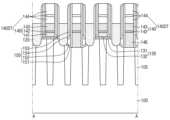
페리 게이트 구조체(240ST)는 페리 영역(24)의 기판(100) 상에 배치될 수 있다. 페리 게이트 구조체(240ST)는 페리 소자 분리막(26)에 의해 정의된 페리 활성 영역 상에 배치될 수 있다.The ferry gate structure (240ST) may be disposed on the substrate (100) of the ferry region (24). The ferry gate structure (240ST) may be disposed on the ferry active region defined by the ferry element isolation film (26).
페리 게이트 구조체(240ST)는 기판(100) 상에 순차적으로 적층된 페리 게이트 절연막(230)과, 페리 게이트 도전막(240)과, 페리 캡핑막(244)을 포함할 수 있다. 페리 게이트 구조체(240ST)는 페리 게이트 도전막(240)의 측벽 및 페리 캡핑막(244)의 측벽 상에 배치된 페리 스페이서(245)를 포함할 수 있다.The ferry gate structure (240ST) may include a ferry gate insulating film (230), a ferry gate conductive film (240), and a ferry capping film (244) sequentially laminated on a substrate (100). The ferry gate structure (240ST) may include a ferry spacer (245) disposed on a sidewall of the ferry gate conductive film (240) and a sidewall of the ferry capping film (244).
페리 게이트 도전막(240)은 페리 게이트 절연막(230) 상에 순차적으로 적층된 제1 내지 제3 페리 도전막(241, 242, 243)을 포함할 수 있다. 일 예로, 페리 게이트 도전막(240)과 페리 게이트 절연막(230) 사이에, 추가적인 도전막이 배치되지 않을 수 있다. 다른 예로, 도시된 것과 달리, 페리 게이트 도전막(240)과 페리 게이트 절연막(230) 사이에, 일함수 도전막과 같은 추가적인 도전막이 배치될 수 있다.The ferry gate conductive film (240) may include first to third ferry conductive films (241, 242, 243) sequentially laminated on the ferry gate insulating film (230). In one example, no additional conductive film may be disposed between the ferry gate conductive film (240) and the ferry gate insulating film (230). In another example, unlike what is illustrated, an additional conductive film, such as a work function conductive film, may be disposed between the ferry gate conductive film (240) and the ferry gate insulating film (230).
인접하는 페리 소자 분리막(26) 사이에, 2개의 페리 게이트 구조체(240ST)가 배치되는 것으로 도시하였지만, 설명의 편의를 위한 것일 뿐, 이에 제한되는 것은 아니다.Although two ferry gate structures (240ST) are shown as being arranged between adjacent ferry element separators (26), this is only for convenience of explanation and is not limited thereto.
제1 블록 도전 구조체(240ST_1)는 셀 영역(20) 및 페리 영역(24) 사이에 배치될 수 있다. 제1 블록 도전 구조체(240ST_1)의 일부는 셀 영역 분리막(22)과 중첩되는 것으로 도시하였지만, 이에 제한되는 것은 아니다. 제1 블록 도전 구조체(240ST_1)은 제2 방향(D2)으로 연장된 비트 라인 구조체(140ST)와 제2 방향(D2)으로 최인접한 도전 구조체일 수 있다.The first block challenge structure (240ST_1) may be positioned between the cell region (20) and the peripheral region (24). A portion of the first block challenge structure (240ST_1) is illustrated as overlapping the cell region separator (22), but is not limited thereto. The first block challenge structure (240ST_1) may be a challenge structure that is closest to the bit line structure (140ST) extending in the second direction (D2) in the second direction (D2).
제1 블록 도전 구조체(240ST_1)는 기판(100) 상에 순차적으로 적층된 제1 블록 게이트 절연막(230_1)과, 제1 블록 도전 라인(240_1)과, 제1 블록 캡핑막(244_1)을 포함할 수 있다. 제1 블록 도전 구조체(240ST_1)는 제1 블록 도전 라인(240_1)의 측벽 및 제1 블록 캡핑막(244_1)의 측벽 상에 배치된 제1 블록 스페이서(245_1)를 포함할 수 있다.The first block conductive structure (240ST_1) may include a first block gate insulating film (230_1), a first block conductive line (240_1), and a first block capping film (244_1) sequentially laminated on a substrate (100). The first block conductive structure (240ST_1) may include a first block spacer (245_1) disposed on a sidewall of the first block conductive line (240_1) and a sidewall of the first block capping film (244_1).
제1 블록 도전 라인(240_1)은 제1 블록 게이트 절연막(230_1) 상에 순차적으로 적층된 제1_1 내지 제1_3 블록 도전막(241_1, 242_1, 243_1)을 포함할 수 있다. 제1 블록 게이트 절연막(230_1)과 제1 블록 캡핑막(244_1) 사이의 제1 블록 도전 라인(240_1)의 적층막 구조는 페리 게이트 도전막(240)의 적층막 구조와 동일할 수 있다.The first block conductive line (240_1) may include first to third block conductive films (241_1, 242_1, 243_1) sequentially laminated on the first block gate insulating film (230_1). The laminated film structure of the first block conductive line (240_1) between the first block gate insulating film (230_1) and the first block capping film (244_1) may be identical to the laminated film structure of the peripheral gate conductive film (240).
제2 블록 도전 구조체(240ST_2)는 셀 영역(20) 및 페리 영역(24) 사이에 배치될 수 있다. 제2 블록 도전 구조체(240ST_2)의 일부는 셀 영역 분리막(22)과 중첩되는 것으로 도시하였지만, 이에 제한되는 것은 아니다. 제2 블록 도전 구조체(240ST_2)는 더미 비트 라인 구조체(140ST_1)와 제1 방향(D1)으로 최인접한 도전 구조체일 수 있다.The second block challenge structure (240ST_2) may be positioned between the cell region (20) and the peripheral region (24). A portion of the second block challenge structure (240ST_2) is illustrated as overlapping the cell region separator (22), but is not limited thereto. The second block challenge structure (240ST_2) may be the challenge structure that is closest to the dummy bit line structure (140ST_1) in the first direction (D1).
제2 블록 도전 구조체(240ST_2)는 기판(100) 상에 순차적으로 적층된 제2 블록 게이트 절연막(230_2)과, 제2 블록 도전 라인(240_2)과, 제2 블록 캡핑막(244_2)을 포함할 수 있다. 제2 블록 도전 구조체(240ST_2)는 제2 블록 도전 라인(240_2)의 측벽 및 제2 블록 캡핑막(244_2)의 측벽 상에 배치된 제2 블록 스페이서(245_2)를 포함할 수 있다.The second block conductive structure (240ST_2) may include a second block gate insulating film (230_2), a second block conductive line (240_2), and a second block capping film (244_2) sequentially laminated on a substrate (100). The second block conductive structure (240ST_2) may include a second block spacer (245_2) disposed on a sidewall of the second block conductive line (240_2) and a sidewall of the second block capping film (244_2).
제2 블록 도전 라인(240_2)은 제2 블록 게이트 절연막(230_2) 상에 순차적으로 적층된 제2_1 내지 제2_3 블록 도전막(241_2, 242_2, 243_2)을 포함할 수 있다. 제2 블록 게이트 절연막(230_2)과 제2 블록 캡핑막(244_2) 사이의 제2 블록 도전 라인(240_2)의 적층막 구조는 페리 게이트 도전막(240)의 적층막 구조와 동일할 수 있다.The second block conductive line (240_2) may include second_1 to second_3 block conductive films (241_2, 242_2, 243_2) sequentially laminated on the second block gate insulating film (230_2). The laminated film structure of the second block conductive line (240_2) between the second block gate insulating film (230_2) and the second block capping film (244_2) may be identical to the laminated film structure of the peripheral gate conductive film (240).
페리 게이트 구조체(240ST)와, 제1 블록 도전 구조체(240ST_1)와, 제1 블록 도전 구조체(240ST_1)는 동일 레벨에서 형성될 수 있다. 페리 게이트 도전막(240)과, 제1 블록 도전 라인(240_1)과, 제2 블록 도전 라인(240_2)은 셀 도전 라인(140)과 동일한 적층 구조를 가질 수 있다. 예를 들어, 페리 게이트 도전막(240)의 두께(T21)는 셀 도전 라인(140)의 두께(T11)과 동일할 수 있다.The ferry gate structure (240ST), the first block conductive structure (240ST_1), and the first block conductive structure (240ST_1) can be formed at the same level. The ferry gate conductive film (240), the first block conductive line (240_1), and the second block conductive line (240_2) can have the same laminated structure as the cell conductive line (140). For example, the thickness (T21) of the ferry gate conductive film (240) can be the same as the thickness (T11) of the cell conductive line (140).
제1 페리 도전막(241)과, 제1_1 블록 도전막(241_1)과, 제2_1 블록 도전막(241_2)은 제1 셀 도전막(141)과 동일한 물질을 포함할 수 있다. 제2 페리 도전막(242)과, 제1_2 블록 도전막(242_1)과, 제2_2 블록 도전막(242_2)은 제2 셀 도전막(142)과 동일한 물질을 포함할 수 있다. 제3 페리 도전막(243)과, 제1_3 블록 도전막(243_1)과, 제2_3 블록 도전막(243_2)은 제3 셀 도전막(143)과 동일한 물질을 포함할 수 있다.The first ferry conductive film (241), the 1_1 block conductive film (241_1), and the 2_1 block conductive film (241_2) may include the same material as the first cell conductive film (141). The second ferry conductive film (242), the 1_2 block conductive film (242_1), and the 2_2 block conductive film (242_2) may include the same material as the second cell conductive film (142). The third ferry conductive film (243), the 1_3 block conductive film (243_1), and the 2_3 block conductive film (243_2) may include the same material as the third cell conductive film (143).
페리 게이트 절연막(230)과, 제1 블록 게이트 절연막(230_1)과, 제2 블록 게이트 절연막(230_2)는 동일한 물질을 포함할 수 있다. 페리 게이트 절연막(230)과, 제1 블록 게이트 절연막(230_1)과, 제2 블록 게이트 절연막(230_2)는 예를 들어, 실리콘 산화물, 실리콘 질화물, 실리콘 산질화물, 또는 실리콘 산화물보다 높은 유전 상수를 갖는 고유전율 물질을 포함할 수 있다.The ferry gate insulating film (230), the first block gate insulating film (230_1), and the second block gate insulating film (230_2) may include the same material. The ferry gate insulating film (230), the first block gate insulating film (230_1), and the second block gate insulating film (230_2) may include, for example, silicon oxide, silicon nitride, silicon oxynitride, or a high-k material having a higher dielectric constant than silicon oxide.
페리 스페이서(245)와, 제1 블록 스페이서(245_1)와, 제2 블록 스페이서(245_2)는 동일한 물질을 포함할 수 있다. 페리 스페이서(245)와, 제1 블록 스페이서(245_1)와, 제2 블록 스페이서(245_2)는 예를 들어, 실리콘 질화물, 실리콘 산질화물, 실리콘 산화물, 실리콘 탄질화물, 실리콘 산탄질화물 및 이들의 조합 중 적어도 하나를 포함할 수 있다. 페리 스페이서(245)와, 제1 블록 스페이서(245_1)와, 제2 블록 스페이서(245_2)는 단일막인 것으로 도시되었지만, 설명의 편의를 위한 것일 뿐, 이에 제한되는 것은 아니다. 페리 스페이서(245)와, 제1 블록 스페이서(245_1)와, 제2 블록 스페이서(245_2)는 다중막일 수 있음은 물론이다.The peripheral spacer (245), the first block spacer (245_1), and the second block spacer (245_2) may include the same material. The peripheral spacer (245), the first block spacer (245_1), and the second block spacer (245_2) may include, for example, at least one of silicon nitride, silicon oxynitride, silicon oxide, silicon carbon nitride, silicon oxycarbon nitride, and combinations thereof. The peripheral spacer (245), the first block spacer (245_1), and the second block spacer (245_2) are illustrated as being single-layered, but this is only for convenience of explanation and is not limited thereto. It goes without saying that the peripheral spacer (245), the first block spacer (245_1), and the second block spacer (245_2) may be multi-layered.
페리 캡핑막(244)과, 제1 블록 캡핑막(244_1)과, 제2 블록 캡핑막(244_2)은 동일한 물질을 포함할 수 있다. 페리 캡핑막(244)과, 제1 블록 캡핑막(244_1)과, 제2 블록 캡핑막(244_2)는 예를 들어, 실리콘 질화막, 실리콘 산질화물 및 실리콘 산화물 중 적어도 하나를 포함할 수 있다.The ferry capping film (244), the first block capping film (244_1), and the second block capping film (244_2) may include the same material. The ferry capping film (244), the first block capping film (244_1), and the second block capping film (244_2) may include, for example, at least one of a silicon nitride film, silicon oxynitride, and silicon oxide.
예를 들어, 페리 캡핑막(244)의 두께(T22)는 셀 라인 캡핑막(144)의 두께(T12)보다 작다. 또한, 기판(100)의 상면을 기준으로, 페리 캡핑막의 상면(244US)은 셀 라인 캡핑막의 상면(144US)보다 낮다. 패드 분리 절연막(180)은 셀 라인 캡핑막(144)의 일부가 제거된 위치에 형성될 수 있다. 그러므로, 도 4, 도 6 및 도 7에서 도시된 것과 같이, 서로 다른 방향 및 서로 다른 영역을 절단한 단면도에서, 셀 라인 캡핑막(144)의 두께는 서로 다르게 보일 수 있다. 몇몇 실시예들에 따른 반도체 메모리 장치에서, 셀 라인 캡핑막(144)의 두께(T12)는 도 4에서 도시된 셀 도전 라인(140) 상의 셀 라인 캡핑막(144)의 두께일 수 있다. 도 4는 셀 영역(20)에서 제2 방향(D2)으로 인접하는 셀 게이트 구조체(110) 사이를 제1 방향(D1)으로 절단한 단면도일 수 있다.For example, the thickness (T22) of the peripheral capping film (244) is smaller than the thickness (T12) of the cell line capping film (144). In addition, with respect to the upper surface of the substrate (100), the upper surface (244US) of the peripheral capping film is lower than the upper surface (144US) of the cell line capping film. The pad separation insulating film (180) may be formed at a location where a portion of the cell line capping film (144) is removed. Therefore, as illustrated in FIGS. 4, 6, and 7, the thicknesses of the cell line capping film (144) may appear different in cross-sectional views cut in different directions and different areas. In the semiconductor memory device according to some embodiments, the thickness (T12) of the cell line capping film (144) may be the thickness of the cell line capping film (144) on the cell conductive line (140) illustrated in FIG. 4. FIG. 4 may be a cross-sectional view taken in the first direction (D1) between adjacent cell gate structures (110) in the second direction (D2) in the cell region (20).
제2 식각 정지막(250)은 기판(100) 상에 배치될 수 있다. 제2 식각 정지막(250)은 페리 게이트 구조체(240ST)의 프로파일과, 제1 블록 도전 구조체(240ST_1)의 프로파일과, 제2 블록 도전 구조체(240ST_2)의 프로파일을 따라 형성될 수 있다. 제2 식각 정지막(250)은 제1 셀 경계 스페이서(246_1) 및 제2 셀 경계 스페이서(246_2)의 측벽을 따라 연장될 수 있다.A second etching stop film (250) may be disposed on the substrate (100). The second etching stop film (250) may be formed along the profile of the ferry gate structure (240ST), the profile of the first block conductive structure (240ST_1), and the profile of the second block conductive structure (240ST_2). The second etching stop film (250) may extend along the sidewalls of the first cell boundary spacer (246_1) and the second cell boundary spacer (246_2).
제2 식각 정지막(250)는 예를 들어, 실리콘 질화막, 실리콘 산질화물, 실리콘 탄질화물 및 실리콘 산탄질화물 중 적어도 하나를 포함할 수 있다.The second etching stop film (250) may include, for example, at least one of silicon nitride, silicon oxynitride, silicon carbon nitride, and silicon oxycarbon nitride.
제1 페리 층간 절연막(290)은 제2 식각 정지막(250) 상에 배치될 수 있다. 제1 페리 층간 절연막(290)은 페리 게이트 구조체(240ST)의 주변에 배치될 수 있다.The first ferry interlayer insulating film (290) may be disposed on the second etching stop film (250). The first ferry interlayer insulating film (290) may be disposed around the ferry gate structure (240ST).
셀 층간 절연막(295)은 제2 식각 정지막(250) 상에 배치될 수 있다. 예를 들어, 셀 층간 절연막(295)은 셀 영역 분리막(22) 상에 배치될 수 있다. 셀 층간 절연막(295)은 제1 블록 도전 구조체(240ST_1) 및 비트 라인 구조체(140ST) 사이와, 제2 블록 도전 구조체(240ST_2) 및 더미 비트 라인 구조체(140ST_1) 사이에 배치될 수 있다. 셀 층간 절연막(295)은 제2 방향(D2)으로 마주보는 셀 도전 라인(140) 및 제1 블록 도전 라인(240_1) 사이와, 제1 방향(D1)으로 마주보는 제2 블록 도전 라인(240_2) 및 더미 비트 라인 구조체(140ST_1)의 셀 도전 라인 사이에 배치될 수 있다. 셀 층간 절연막(295)은 비트 라인 구조체(140ST) 및 더미 비트 라인 구조체(140ST_1) 주변에 배치될 수 있다.The cell interlayer insulating film (295) may be disposed on the second etching stop film (250). For example, the cell interlayer insulating film (295) may be disposed on the cell area separator film (22). The cell interlayer insulating film (295) may be disposed between the first block conductive structure (240ST_1) and the bit line structure (140ST), and between the second block conductive structure (240ST_2) and the dummy bit line structure (140ST_1). The cell interlayer insulating film (295) may be disposed between the cell conductive line (140) and the first block conductive line (240_1) facing each other in the second direction (D2), and between the cell conductive line of the second block conductive line (240_2) and the dummy bit line structure (140ST_1) facing each other in the first direction (D1). The cell interlayer insulating film (295) can be placed around the bit line structure (140ST) and the dummy bit line structure (140ST_1).
제1 페리 층간 절연막(290) 및 셀 층간 절연막(295)은 동일 레벨에서 형성될 수 있다. 제1 페리 층간 절연막(290) 및 셀 층간 절연막(295)은 동일한 물질을 포함할 수 있다. 제1 페리 층간 절연막(290) 및 셀 층간 절연막(295)은 예를 들어, 산화물 계열의 절연 물질을 포함할 수 있다.The first ferry interlayer insulating film (290) and the cell interlayer insulating film (295) can be formed at the same level. The first ferry interlayer insulating film (290) and the cell interlayer insulating film (295) can include the same material. The first ferry interlayer insulating film (290) and the cell interlayer insulating film (295) can include, for example, an oxide-based insulating material.
예를 들어, 페리 게이트 구조체(240ST)는 인접하는 페리 소자 분리막(26) 내에 배치된 제1 페리 게이트 구조체 및 제2 페리 게이트 구조체를 포함할 수 있다. 제1 페리 게이트 구조체는 제2 페리 게이트 구조체과 이격된다. 또한, 페리 게이트 구조체(240ST)는 페리 소자 분리막(26)을 사이에 두고 제1 페리 게이트 구조체와 이격된 제3 페리 게이트 구조체를 포함할 수 있다. 제1 내지 제3 페리 게이트 구조체는 각각 페리 게이트 절연막(230)과, 페리 게이트 도전막(240)과, 페리 캡핑막(244)과 페리 스페이서(245)를 포함한다.For example, the ferry gate structure (240ST) may include a first ferry gate structure and a second ferry gate structure disposed within adjacent ferry element isolation films (26). The first ferry gate structure is spaced apart from the second ferry gate structure. In addition, the ferry gate structure (240ST) may include a third ferry gate structure spaced apart from the first ferry gate structure with the ferry element isolation film (26) interposed therebetween. The first to third ferry gate structures each include a ferry gate insulating film (230), a ferry gate conductive film (240), a ferry capping film (244), and a ferry spacer (245).
제1 페리 게이트 구조체에 포함된 페리 게이트 도전막(240)은 제2 페리 게이트 구조체에 포함된 페리 게이트 도전막(240)과 제1 거리(L1)만큼 이격될 수 있다. 제1 페리 게이트 구조체에 포함된 페리 게이트 도전막(240)은 제3 페리 게이트 구조체에 포함된 페리 게이트 도전막(240)과 제2 거리(L1)만큼 이격될 수 있다. 몇몇 실시예들에 따른 반도체 메모리 장치에서, 제1 거리(L1)는 제2 거리(L2)와 다를 수 있다. 예를 들어, 제1 거리(L1)는 제2 거리(L2)보다 작다.The ferry gate conductive film (240) included in the first ferry gate structure can be spaced apart from the ferry gate conductive film (240) included in the second ferry gate structure by a first distance (L1). The ferry gate conductive film (240) included in the first ferry gate structure can be spaced apart from the ferry gate conductive film (240) included in the third ferry gate structure by a second distance (L1). In a semiconductor memory device according to some embodiments, the first distance (L1) can be different from the second distance (L2). For example, the first distance (L1) is smaller than the second distance (L2).
기판(100)의 상면을 기준으로, 제1 페리 게이트 구조체에 포함된 페리 게이트 도전막(240)과 제2 페리 게이트 구조체에 포함된 페리 게이트 도전막(240) 사이에서, 제1 페리 층간 절연막의 상면(290US)의 높이는 제1 높이(H1)일 수 있다. 기판(100)의 상면을 기준으로, 제1 페리 게이트 구조체에 포함된 페리 게이트 도전막(240)과 제3 페리 게이트 구조체에 포함된 페리 게이트 도전막(240) 사이에서, 제1 페리 층간 절연막의 상면(290US)의 높이는 제2 높이(H2)일 수 있다. 기판(100)의 상면을 기준으로, 제1 내지 제3 페리 게이트 구조체의 페리 캡핑막의 상면(244US)의 높이는 제3_1 높이(H31)일 수 있다. 기판(100)의 상면을 기준으로, 제1 내지 제3 페리 게이트 구조체의 페리 스페이서(245)의 최상부의 높이는 제3_2 높이(H31)일 수 있다.With respect to the upper surface of the substrate (100), the height of the upper surface (290US) of the first Ferry interlayer insulating film between the Ferry gate conductive film (240) included in the first Ferry gate structure and the Ferry gate conductive film (240) included in the second Ferry gate structure may be a first height (H1). With respect to the upper surface of the substrate (100), the height of the upper surface (290US) of the first Ferry interlayer insulating film between the Ferry gate conductive film (240) included in the first Ferry gate structure and the Ferry gate conductive film (240) included in the third Ferry gate structure may be a second height (H2). With respect to the upper surface of the substrate (100), the height of the upper surfaces (244US) of the Ferry capping films of the first to third Ferry gate structures may be a third_1 height (H31). Based on the upper surface of the substrate (100), the height of the uppermost portion of the peripheral spacer (245) of the first to third peripheral gate structures may be the third_2 height (H31).
기판(100)의 상면을 기준으로, 제1 페리 층간 절연막의 상면(290US)은 페리 캡핑막의 상면(244US)보다 낮다. 예를 들어, 제3_1 높이(H31)는 제1 높이(H1) 및 제2 높이(H2)보다 크다. 몇몇 실시예들에 따른 반도체 장치에서, 제1 높이(H1)는 제2 높이(H2)와 동일할 수 있다.Based on the upper surface of the substrate (100), the upper surface (290US) of the first ferry interlayer insulating film is lower than the upper surface (244US) of the ferry capping film. For example, the third_1 height (H31) is greater than the first height (H1) and the second height (H2). In a semiconductor device according to some embodiments, the first height (H1) may be equal to the second height (H2).
기판(100)의 상면을 기준으로, 제1 페리 층간 절연막의 상면(290US)은 페리 스페이서(245)의 최상부보다 낮을 수 있다. 일 예로, 제3_1 높이(H31)는 제3_2 높이(H32)와 동일할 수 있다. 이와 같은 경우, 제3_2 높이(H32)는 제1 높이(H1) 및 제2 높이(H2)보다 크다.Based on the upper surface of the substrate (100), the upper surface (290US) of the first ferry interlayer insulating film may be lower than the uppermost portion of the ferry spacer (245). For example, the 3_1 height (H31) may be the same as the 3_2 height (H32). In this case, the 3_2 height (H32) is greater than the first height (H1) and the second height (H2).
도시된 것과 달리, 다른 예로, 제조 공정 중의 식각 공정에 의해, 페리 스페이서(245)의 최상부는 페리 캡핑막의 상면(244US)보다 낮아질 수 있다. 이와 같은 경우, 제3_2 높이(H32)는 제1 높이(H1) 및 제2 높이(H2)보다 크거나 같을 수 있다.Unlike the illustrated example, in another example, the uppermost portion of the ferry spacer (245) may be lowered than the upper surface (244US) of the ferry capping film by an etching process during the manufacturing process. In this case, the third_2 height (H32) may be greater than or equal to the first height (H1) and the second height (H2).
기판(100)의 상면을 기준으로, 제1 블록 도전 구조체(240ST_1) 및 비트 라인 구조체(140ST) 사이에서 셀 층간 절연막의 상면(295US)의 높이는 제4 높이(H4)일 수 있다. 기판(100)의 상면을 기준으로, 제2 블록 도전 구조체(240ST_2) 및 더미 비트 라인 구조체(140ST_1) 사이에서 셀 층간 절연막의 상면(295US)의 높이는 제5 높이(H5)일 수 있다.Based on the upper surface of the substrate (100), the height of the upper surface (295US) of the cell interlayer insulating film between the first block conductive structure (240ST_1) and the bit line structure (140ST) may be a fourth height (H4). Based on the upper surface of the substrate (100), the height of the upper surface (295US) of the cell interlayer insulating film between the second block conductive structure (240ST_2) and the dummy bit line structure (140ST_1) may be a fifth height (H5).
기판(100)의 상면을 기준으로, 셀 층간 절연막의 상면(295US)은 제1 블록 캡핑막의 상면(244US_1)보다 낮다. 기판(100)의 상면을 기준으로, 셀 층간 절연막의 상면(295US)은 제2 블록 캡핑막의 상면(244US_2)보다 낮다.Based on the upper surface of the substrate (100), the upper surface (295US) of the cell interlayer insulating film is lower than the upper surface (244US_1) of the first block capping film. Based on the upper surface of the substrate (100), the upper surface (295US) of the cell interlayer insulating film is lower than the upper surface (244US_2) of the second block capping film.
몇몇 실시예들에 따른 반도체 메모리 장치에서, 제4 높이(H4)는 제5 높이(H5)와 동일할 수 있다. 몇몇 실시예들에 따른 반도체 메모리 장치에서, 제4 높이(H4)는 제1 높이(H1) 및 제2 높이(H2)와 동일할 수 있다.In a semiconductor memory device according to some embodiments, the fourth height (H4) may be equal to the fifth height (H5). In a semiconductor memory device according to some embodiments, the fourth height (H4) may be equal to the first height (H1) and the second height (H2).
삽입 층간 절연막(291)은 페리 게이트 구조체(240ST)와, 제1 페리 층간 절연막(290)과, 셀 층간 절연막(295) 상에 배치된다. 삽입 층간 절연막(291)은 페리 게이트 구조체(240ST)와, 제1 페리 층간 절연막(290)과, 셀 층간 절연막(295)을 덮을 수 있다. 삽입 층간 절연막(291)은 제1 페리 층간 절연막의 상면(290US) 및 셀 층간 절연막의 상면(295US)보다 위로 돌출된 제2 식각 정지막(250)을 덮을 수 있다.An interlayer insulating film (291) is disposed on the ferry gate structure (240ST), the first interlayer insulating film (290), and the cell interlayer insulating film (295). The interlayer insulating film (291) can cover the ferry gate structure (240ST), the first interlayer insulating film (290), and the cell interlayer insulating film (295). The interlayer insulating film (291) can cover the second etching stop film (250) that protrudes above the upper surface (290US) of the first interlayer insulating film and the upper surface (295US) of the cell interlayer insulating film.
제1 페리 층간 절연막의 상면(290US) 및 셀 층간 절연막의 상면(295US)은 평면인 것으로 도시되었지만, 이에 제한되는 것은 아니다. 제1 페리 층간 절연막의 상면(290US) 및 셀 층간 절연막의 상면(295US)은 각각 기판(100)을 향해 볼록한 곡면일 수도 있다. 이와 같은 경우, 제1 페리 층간 절연막의 상면(290US) 및 셀 층간 절연막의 상면(295US)의 높이 기준은 기판(100)과 가장 근접한 부분일 수 있다.The upper surface (290US) of the first ferry interlayer insulating film and the upper surface (295US) of the cell interlayer insulating film are illustrated as being flat, but are not limited thereto. The upper surface (290US) of the first ferry interlayer insulating film and the upper surface (295US) of the cell interlayer insulating film may each be a convex curved surface toward the substrate (100). In this case, the height reference of the upper surface (290US) of the first ferry interlayer insulating film and the upper surface (295US) of the cell interlayer insulating film may be the portion closest to the substrate (100).
삽입 층간 절연막(291)은 제1 페리 층간 절연막(290) 및 셀 층간 절연막(295)과 다른 물질을 포함한다. 삽입 층간 절연막(291)은 예를 들어, 질화물 계열의 절연 물질을 포함할 수 있다. 예를 들어, 삽입 층간 절연막(291)은 실리콘 질화물을 포함할 수 있다.The insertion interlayer insulating film (291) includes a different material from the first ferry interlayer insulating film (290) and the cell interlayer insulating film (295). The insertion interlayer insulating film (291) may include, for example, a nitride-based insulating material. For example, the insertion interlayer insulating film (291) may include silicon nitride.
삽입 층간 절연막(291)의 일부는 인접하는 페리 게이트 구조체(240ST) 사이에 만입된다. 즉, 기판(100)의 상면을 기준으로, 삽입 층간 절연막(291)의 하면은 페리 캡핑막의 상면(244US)보다 낮다.A portion of the interlayer insulating film (291) is indented between adjacent ferry gate structures (240ST). That is, with respect to the upper surface of the substrate (100), the lower surface of the interlayer insulating film (291) is lower than the upper surface (244US) of the ferry capping film.
이를 통해, 정보 저장부(190)를 제조하는 과정에 포함된 식각 공정에서, 삽입 층간 절연막(291)은 제1 페리 층간 절연막(290)을 보호할 수 있다. 정보 저장부(190)를 제조하는 과정에 포함된 식각 공정에서, 삽입 층간 절연막(291)은 제1 페리 층간 절연막(290)이 식각되어 발생되는 불량을 방지할 수 있다.Through this, in the etching process included in the process of manufacturing the information storage unit (190), the insertion interlayer insulating film (291) can protect the first ferry interlayer insulating film (290). In the etching process included in the process of manufacturing the information storage unit (190), the insertion interlayer insulating film (291) can prevent defects caused by the etching of the first ferry interlayer insulating film (290).
페리 컨택 플러그(260)은 페리 게이트 구조체(240ST)의 양측에 배치될 수 있다. 페리 컨택 플러그(260)은 삽입 층간 절연막(291) 및 제1 페리 층간 절연막(290)을 관통하여, 페리 영역(24)의 기판(100)까지 연장될 수 있다.The ferry contact plug (260) may be arranged on both sides of the ferry gate structure (240ST). The ferry contact plug (260) may extend to the substrate (100) of the ferry region (24) by penetrating the insertion interlayer insulating film (291) and the first ferry interlayer insulating film (290).
페리 배선 라인(265)은 삽입 층간 절연막(291) 상에 배치될 수 있다. 비트 라인 컨택 플러그(261)은 셀 라인 캡핑막(144)을 통과하여, 셀 도전 라인(140)과 연결될 수 있다. 셀 게이트 컨택 플러그(262)는 삽입 층간 절연막(291)과, 셀 층간 절연막(295)과, 셀 게이트 캡핑 패턴(113)을 통과하여, 셀 게이트 전극(112)과 연결될 수 있다.The ferry wiring line (265) may be arranged on the insertion interlayer insulating film (291). The bit line contact plug (261) may pass through the cell line capping film (144) and be connected to the cell conductive line (140). The cell gate contact plug (262) may pass through the insertion interlayer insulating film (291), the cell interlayer insulating film (295), and the cell gate capping pattern (113) and be connected to the cell gate electrode (112).
페리 컨택 플러그(260)과, 페리 배선 라인(265)과, 비트 라인 컨택 플러그(261)과, 셀 게이트 컨택 플러그(262)는 스토리지 패드(160)와 동일한 물질을 포함할 수 있다.The ferry contact plug (260), the ferry wiring line (265), the bit line contact plug (261), and the cell gate contact plug (262) may include the same material as the storage pad (160).
페리 배선 분리 패턴(280)은 페리 배선 라인(265) 및 페리 컨택 플러그(260)를 분리할 수 있다. 페리 배선 분리 패턴(280)은 예를 들어, 실리콘 산화막, 실리콘 질화막, 실리콘 산질화막, 실리콘 산탄질화막 및 실리콘 탄질화막 중 적어도 하나를 포함할 수 있다.The ferry wiring separation pattern (280) can separate the ferry wiring line (265) and the ferry contact plug (260). The ferry wiring separation pattern (280) can include, for example, at least one of a silicon oxide film, a silicon nitride film, a silicon oxynitride film, a silicon carbonitride film, and a silicon carbonitride film.
제1 식각 정지막(292)는 페리 컨택 플러그(260)과, 페리 배선 라인(265)과, 비트 라인 컨택 플러그(261)과, 셀 게이트 컨택 플러그(262) 상에 배치될 수 있다.The first etching stop film (292) can be placed on the ferry contact plug (260), the ferry wiring line (265), the bit line contact plug (261), and the cell gate contact plug (262).
제2 페리 층간 절연막(293)은 제1 식각 정지막(292) 상에 배치될 수 있다. 제2 페리 층간 절연막(293)은 제1 상부 전극(193)의 측벽을 덮을 수 있다. 제2 페리 층간 절연막(293)은 절연 물질을 포함할 수 있다.A second ferri interlayer insulating film (293) may be disposed on the first etching stop film (292). The second ferri interlayer insulating film (293) may cover a sidewall of the first upper electrode (193). The second ferri interlayer insulating film (293) may include an insulating material.
도 9는 몇몇 실시예들에 따른 반도체 메모리 장치를 설명하기 위한 도면이다. 도 10은 몇몇 실시예들에 따른 반도체 메모리 장치를 설명하기 위한 도면이다. 설명의 편의상, 도 1 내지 도 8을 이용하여 설명한 것과 다른 점을 중심으로 설명한다.FIG. 9 is a drawing for explaining a semiconductor memory device according to some embodiments. FIG. 10 is a drawing for explaining a semiconductor memory device according to some embodiments. For convenience of explanation, the explanation will focus on differences from those explained using FIGS. 1 to 8.
참고적으로, 도 9는 도 2의 C - C를 따라 절단한 단면도이고, 도 10은 도 2의 E - E를 따라 절단한 단면도이다.For reference, Fig. 9 is a cross-sectional view taken along line C-C of Fig. 2, and Fig. 10 is a cross-sectional view taken along line E-E of Fig. 2.
도 8 및 도 9를 참고하면, 몇몇 실시예들에 따른 반도체 장치에서, 기판(100)의 상면을 기준으로, 제1 페리 층간 절연막의 상면(290US)은 제1 블록 도전 구조체(240ST_1) 및 비트 라인 구조체(140ST) 사이에서 셀 층간 절연막의 상면(295US)보다 높다.Referring to FIGS. 8 and 9, in a semiconductor device according to some embodiments, with respect to the upper surface of the substrate (100), the upper surface (290US) of the first ferry interlayer insulating film is higher than the upper surface (295US) of the cell interlayer insulating film between the first block conductive structure (240ST_1) and the bit line structure (140ST).
기판(100)의 상면을 기준으로, 제1 페리 층간 절연막의 상면(290US)의 높이(H1, H2)는 제1 블록 도전 구조체(240ST_1) 및 비트 라인 구조체(140ST) 사이에서 셀 층간 절연막의 상면(295US)의 높이(H4)보다 크다.Based on the upper surface of the substrate (100), the height (H1, H2) of the upper surface (290US) of the first interlayer insulating film is greater than the height (H4) of the upper surface (295US) of the cell interlayer insulating film between the first block conductive structure (240ST_1) and the bit line structure (140ST).
도 10을 참고하면, 몇몇 실시예들에 따른 반도체 메모리 장치에서, 제1 거리(L1)만큼 이격된 페리 게이트 도전막(240) 사이에서 제1 페리 층간 절연막의 상면(290US)의 높이(H1)는, 제2 거리(L2)만큼 이격된 페리 게이트 도전막(240) 사이에서 제1 페리 층간 절연막의 상면(290US)의 높이(H2)와 다를 수 있다.Referring to FIG. 10, in a semiconductor memory device according to some embodiments, a height (H1) of an upper surface (290US) of a first interlayer insulating film between the peripheral gate conductive films (240) spaced apart by a first distance (L1) may be different from a height (H2) of an upper surface (290US) of the first interlayer insulating film between the peripheral gate conductive films (240) spaced apart by a second distance (L2).
예를 들어, 제1 페리 게이트 구조체 및 제2 페리 게이트 구조체 사이의 제1 페리 층간 절연막의 상면(290US)의 높이(H1)는, 제1 페리 게이트 구조체 및 제3 페리 게이트 구조체 사이의 제1 페리 층간 절연막의 상면(290US)의 높이(H2)보다 크다.For example, the height (H1) of the upper surface (290US) of the first interlayer insulating film between the first and second peripheral gate structures is greater than the height (H2) of the upper surface (290US) of the first interlayer insulating film between the first and third peripheral gate structures.
다르게 설명하면, 인접하는 페리 게이트 도전막(240) 사이의 거리가 증가함에 따라, 기판(100)의 상면을 기준으로, 인접하는 페리 게이트 도전막(240) 사이의 제1 페리 층간 절연막의 상면(290US)의 높이는 작아질 수 있다.In other words, as the distance between adjacent ferry gate conductive films (240) increases, the height of the upper surface (290US) of the first ferry interlayer insulating film between adjacent ferry gate conductive films (240) may decrease with respect to the upper surface of the substrate (100).
도시되지 않았지만, 일 예로, 제1 블록 도전 구조체(240ST_1) 및 비트 라인 구조체(140ST)가 제2 방향(D2)으로 이격된 거리가 변함에 따라, 제1 블록 도전 구조체(240ST_1) 및 비트 라인 구조체(140ST) 사이에서 셀 층간 절연막의 상면(295US)의 높이(H4)도 변할 수 있다. 다른 예로, 제2 블록 도전 구조체(240ST_2) 및 더미 비트 라인 구조체(140ST_1)가 제1 방향(D1)으로 이격된 거리가 변함에 따라, 제2 블록 도전 구조체(240ST_2) 및 더미 비트 라인 구조체(140ST_1) 사이에서 셀 층간 절연막의 상면(295US)의 높이(H5)도 변할 수 있다.Although not illustrated, as an example, as the distance between the first block conductive structure (240ST_1) and the bit line structure (140ST) in the second direction (D2) changes, the height (H4) of the upper surface (295US) of the cell interlayer insulating film between the first block conductive structure (240ST_1) and the bit line structure (140ST) may also change. As another example, as the distance between the second block conductive structure (240ST_2) and the dummy bit line structure (140ST_1) in the first direction (D1) changes, the height (H5) of the upper surface (295US) of the cell interlayer insulating film between the second block conductive structure (240ST_2) and the dummy bit line structure (140ST_1) may also change.
도 11은 몇몇 실시예들에 따른 반도체 메모리 장치를 설명하기 위한 레이아웃도이다. 도 12는 몇몇 실시예들에 따른 반도체 메모리 장치를 설명하기 위한 사시도이다. 도 13은 도 11의 F - F 및 G - G를 따라 절단한 단면도이다. 참고적으로, 도 11은 도 2의 셀 영역(20)을 확대한 도면일 수 있다. 또한, 도 11이 셀 영역에 적용된 반도체 메모리 장치에서, 셀 영역의 경계 부분의 단면(예를 들어, 도 2의 C - C 및 D - D)은 도 6 및 도 7과 상이하다.FIG. 11 is a layout diagram for explaining a semiconductor memory device according to some embodiments. FIG. 12 is a perspective view for explaining a semiconductor memory device according to some embodiments. FIG. 13 is a cross-sectional view taken along lines F-F and G-G of FIG. 11. For reference, FIG. 11 may be an enlarged view of the cell region (20) of FIG. 2. In addition, in the semiconductor memory device to which FIG. 11 is applied to the cell region, a cross-section of a boundary portion of the cell region (for example, C-C and D-D of FIG. 2) is different from FIGS. 6 and 7.
도 11 내지 도 13을 참고하면, 몇몇 실시예들에 따른 반도체 메모리 장치는 기판(100), 복수의 제1 도전 라인(420), 채널층(430), 게이트 전극(440), 게이트 절연막(450) 및 커패시터(480)를 포함할 수 있다. 몇몇 실시예들에 따른 반도체 메모리 장치는 수직 채널 트랜지스터(vertical channel transistor, VCT)를 포함하는 메모리 장치일 수 있다. 상기 수직 채널 트랜지스터는, 채널층(430)의 채널 길이가 기판(100)으로부터 수직 방향을 따라 연장되는 구조를 가리킬 수 있다.Referring to FIGS. 11 to 13, a semiconductor memory device according to some embodiments may include a substrate (100), a plurality of first conductive lines (420), a channel layer (430), a gate electrode (440), a gate insulating film (450), and a capacitor (480). The semiconductor memory device according to some embodiments may be a memory device including a vertical channel transistor (VCT). The vertical channel transistor may refer to a structure in which a channel length of a channel layer (430) extends in a vertical direction from the substrate (100).
기판(100) 상에는 하부 절연층(412)이 배치될 수 있다. 하부 절연층(412) 상에 복수의 제1 도전 라인(420)이 제1 방향(D1)으로 서로 이격되고 제2 방향(D2)으로 연장될 수 있다. 하부 절연층(412) 상에는 복수의 제1 절연 패턴(422)이 복수의 제1 도전 라인(420) 사이의 공간을 채우도록 배치될 수 있다. 복수의 제1 절연 패턴(422)은 제2 방향(D2)으로 연장될 수 있다. 복수의 제1 절연 패턴(422)의 상면은 복수의 제1 도전 라인(420)의 상면과 동일 레벨에 배치될 수 있다. 복수의 제1 도전 라인(420)은 비트 라인으로 기능할 수 있다.A lower insulating layer (412) may be arranged on a substrate (100). A plurality of first conductive lines (420) may be spaced apart from each other in a first direction (D1) and extended in a second direction (D2) on the lower insulating layer (412). A plurality of first insulating patterns (422) may be arranged on the lower insulating layer (412) to fill spaces between the plurality of first conductive lines (420). The plurality of first insulating patterns (422) may extend in the second direction (D2). Upper surfaces of the plurality of first insulating patterns (422) may be arranged at the same level as upper surfaces of the plurality of first conductive lines (420). The plurality of first conductive lines (420) may function as bit lines.
복수의 제1 도전 라인(420)은 도핑된 반도체 물질, 금속, 도전성 금속 질화물, 도전성 금속 실리사이드, 도전성 금속 산화물, 또는 이들의 조합을 포함할 수 있다. 예를 들면, 복수의 제1 도전 라인(420)은 도핑된 폴리 실리콘, Al, Cu, Ti, Ta, Ru, W, Mo, Pt, Ni, Co, TiN, TaN, WN, NbN, TiAl, TiAlN, TiSi, TiSiN, TaSi, TaSiN, RuTiN, NiSi, CoSi, IrOx, RuOx, 또는 이들의 조합으로 이루어질 수 있으나, 이에 한정되는 것은 아니다. 복수의 제1 도전 라인(420)은 전술한 물질들의 단일층 또는 다중층을 포함할 수 있다. 예시적인 실시예들에서, 복수의 제1 도전 라인(420)은 그래핀(graphene), 탄소 나노 튜브(carbon nanotube) 또는 이들의 조합을 포함할 수 있다.The plurality of first conductive lines (420) may include a doped semiconductor material, a metal, a conductive metal nitride, a conductive metal silicide, a conductive metal oxide, or a combination thereof. For example, the plurality of first conductive lines (420) may be formed of, but are not limited to, doped polysilicon, Al, Cu, Ti, Ta, Ru, W, Mo, Pt, Ni, Co, TiN, TaN, WN, NbN, TiAl, TiAlN, TiSi, TiSiN, TaSi, TaSiN, RuTiN, NiSi, CoSi, IrOx, RuOx, or a combination thereof. The plurality of first conductive lines (420) may include a single layer or multiple layers of the materials described above. In exemplary embodiments, the plurality of first conductive lines (420) may include graphene, carbon nanotubes, or a combination thereof.
채널층(430)은 복수의 제1 도전 라인(420) 상에서 제1 방향(D1) 및 제2 방향(D2)으로 이격되어 배치되는 매트릭스 형태로 배열될 수 있다. 채널층(430)은 제1 방향(D1)에 따른 제1 폭과 제4 방향(D4)에 따른 제1 높이를 가질 수 있고, 제1 높이가 제1 폭보다 더 클 수 있다. 여기에서 제4 방향(D4)은 제1 방향(D1) 및 제2 방향(D2)과 교차하고, 예를 들어, 기판(100)의 상면과 수직인 방향일 수 있다. 예를 들어, 상기 제1 높이는 상기 제1 폭의 약 2 내지 10배일 수 있으나, 이에 한정되는 것은 아니다. 채널층(430)의 바닥부는 제3 소오스/드레인 영역(도시 생략)으로 기능하고, 채널층(430)의 상부(upper portion)는 제4 소오스/드레인 영역(도시 생략)으로 기능하며, 상기 제3 및 제4 소오스/드레인 영역 사이의 채널층(430)의 일부분은 채널 영역(도시 생략)으로 기능할 수 있다.The channel layer (430) may be arranged in a matrix form spaced apart from each other in the first direction (D1) and the second direction (D2) on a plurality of first conductive lines (420). The channel layer (430) may have a first width along the first direction (D1) and a first height along the fourth direction (D4), and the first height may be greater than the first width. Here, the fourth direction (D4) may intersect the first direction (D1) and the second direction (D2), and may be, for example, a direction perpendicular to the upper surface of the substrate (100). For example, the first height may be about 2 to 10 times the first width, but is not limited thereto. The bottom portion of the channel layer (430) functions as a third source/drain region (not shown), the upper portion of the channel layer (430) functions as a fourth source/drain region (not shown), and a portion of the channel layer (430) between the third and fourth source/drain regions can function as a channel region (not shown).
예시적인 실시예들에서, 채널층(430)은 산화물 반도체를 포함할 수 있고, 예를 들어, 상기 산화물 반도체는 InxGayZnzO, InxGaySizO, InxSnyZnzO, InxZnyO, ZnxO, ZnxSnyO, ZnxOyN, ZrxZnySnzO, SnxO, HfxInyZnzO, GaxZnySnzO, AlxZnySnzO, YbxGayZnzO, InxGayO 또는 이들의 조합을 포함할 수 있다. 채널층(430)은 상기 산화물 반도체의 단일층 또는 다중층을 포함할 수 있다. 일부 예시들에서, 채널층(430)은 실리콘의 밴드갭 에너지보다 더 큰 밴드갭 에너지를 가질 수 있다. 예를 들어, 채널층(430)은 약 1.5 eV 내지 5.6 eV의 밴드갭 에너지를 가질 수 있다. 예를 들어, 채널층(430)은 약 2.0 eV 내지 4.0 eV의 밴드갭 에너지를 가질 때 최적의 채널 성능을 가질 수 있다. 예를 들어, 채널층(430)은 다결정 또는 비정질일 수 있으나, 이에 한정되는 것은 아니다. 예시적인 실시예들에서, 채널층(430)은 그래핀(graphene), 탄소 나노 튜브(carbon nanotube) 또는 이들의 조합을 포함할 수 있다.In exemplary embodiments, the channel layer (430) may include an oxide semiconductor, for example, the oxide semiconductor may include Inx Gay Znz O, Inx Gay Siz O, Inx Sny Znz O, Inx Zny O, Znx O, Znx Sny O, Znx Oy N, Zrx Zny Snz O, Snx O, Hfx Iny Znz O, Gax Zny Snz O, Alx Zny Snz O, Ybx Gay Znz O, Inx Gay O, or a combination thereof. The channel layer (430) may include a single layer or multiple layers of the oxide semiconductor. In some examples, the channel layer (430) may have a bandgap energy greater than the bandgap energy of silicon. For example, the channel layer (430) may have a bandgap energy of about 1.5 eV to 5.6 eV. For example, the channel layer (430) may have optimal channel performance when it has a band gap energy of about 2.0 eV to 4.0 eV. For example, the channel layer (430) may be polycrystalline or amorphous, but is not limited thereto. In exemplary embodiments, the channel layer (430) may include graphene, carbon nanotubes, or a combination thereof.
게이트 전극(440)은 채널층(430)의 양 측벽 상에서 제1 방향(D1)으로 연장될 수 있다. 게이트 전극(440)은 채널층(430)의 제1 측벽과 마주보는 제1 서브 게이트 전극(440P1)과, 채널층(430)의 제1 측벽에 반대되는 제2 측벽과 마주보는 제2 서브 게이트 전극(440P2)을 포함할 수 있다. 제1 서브 게이트 전극(440P1)과 제2 서브 게이트 전극(440P2) 사이에 하나의 채널층(430)이 배치됨에 따라 반도체 장치는 듀얼 게이트 트랜지스터 구조를 가질 수 있다. 그러나, 본 발명의 기술적 사상이 이에 한정되는 것은 아니며, 제2 서브 게이트 전극(440P2)이 생략되고 채널층(430)의 제1 측벽과 마주보는 제1 서브 게이트 전극(440P1)만이 형성되어 싱글 게이트 트랜지스터 구조가 구현될 수도 있다. 게이트 전극(440)에 포함된 물질은 셀 게이트 전극(112)에 관한 설명과 동일할 수 있다.The gate electrode (440) may extend in a first direction (D1) on both sidewalls of the channel layer (430). The gate electrode (440) may include a first sub-gate electrode (440P1) facing a first sidewall of the channel layer (430) and a second sub-gate electrode (440P2) facing a second sidewall of the channel layer (430) opposite to the first sidewall. Since one channel layer (430) is disposed between the first sub-gate electrode (440P1) and the second sub-gate electrode (440P2), the semiconductor device may have a dual-gate transistor structure. However, the technical idea of the present invention is not limited thereto, and the second sub-gate electrode (440P2) may be omitted and only the first sub-gate electrode (440P1) facing the first sidewall of the channel layer (430) may be formed, thereby implementing a single-gate transistor structure. The material included in the gate electrode (440) may be the same as the description regarding the cell gate electrode (112).
게이트 절연막(450)은 채널층(430)의 측벽을 둘러싸며, 채널층(430)과 게이트 전극(440) 사이에 개재될 수 있다. 예를 들어, 도 11에 도시된 것과 같이, 채널층(430)의 전체 측벽이 게이트 절연막(450)에 의해 둘러싸일 수 있고, 게이트 전극(440)의 측벽 일부분이 게이트 절연막(450)과 접촉할 수 있다. 다른 실시예들에서, 게이트 절연막(450)은 게이트 전극(440)의 연장 방향(즉, 제1 방향(D1))으로 연장되고, 채널층(430)의 측벽들 중 게이트 전극(440)과 마주보는 두 측벽들만이 게이트 절연막(450)과 접촉할 수도 있다. 예시적인 실시예들에서, 게이트 절연막(450)은 실리콘 산화막, 실리콘 산질화막, 실리콘 산화막보다 높은 유전 상수를 가지는 고유전율 물질, 또는 이들의 조합으로 이루어질 수 있다.The gate insulating film (450) surrounds the sidewall of the channel layer (430) and may be interposed between the channel layer (430) and the gate electrode (440). For example, as illustrated in FIG. 11, the entire sidewall of the channel layer (430) may be surrounded by the gate insulating film (450), and a portion of the sidewall of the gate electrode (440) may be in contact with the gate insulating film (450). In other embodiments, the gate insulating film (450) may extend in the extending direction of the gate electrode (440) (i.e., the first direction (D1)), and only two sidewalls of the channel layer (430) facing the gate electrode (440) may be in contact with the gate insulating film (450). In exemplary embodiments, the gate insulating film (450) may be formed of a silicon oxide film, a silicon oxynitride film, a high-k material having a higher dielectric constant than that of the silicon oxide film, or a combination thereof.
복수의 제1 절연 패턴(422) 상에는 복수의 제2 절연 패턴(432)이 제2 방향(D2)을 따라 연장될 수 있다. 복수의 제2 절연 패턴(432) 중 인접한 2개의 제2 절연 패턴(432) 사이에 채널층(430)이 배치될 수 있다. 또한, 인접한 2개의 제2 절연 패턴(432) 사이에서, 2개의 인접한 채널층(430) 사이의 공간에 제1 매립층(434) 및 제2 매립층(436)이 배치될 수 있다. 제1 매립층(434)은 2개의 인접한 채널층(430) 사이의 공간의 바닥부에 배치될 수 있다. 제2 매립층(436)은 제1 매립층(434) 상에서 2개의 인접한 채널층(430) 사이의 공간의 나머지를 채우도록 형성될 수 있다. 제2 매립층(436)의 상면은 채널층(430)의 상면과 동일한 레벨에 배치되며, 제2 매립층(436)은 제2 게이트 전극(440)의 상면을 덮을 수 있다. 이와는 달리, 복수의 제2 절연 패턴(432)이 복수의 제1 절연 패턴(422)과 연속적인 물질층으로 형성되거나, 제2 매립층(436)이 제1 매립층(434)과 연속적인 물질층으로 형성될 수도 있다.A plurality of second insulating patterns (432) may extend along the second direction (D2) on a plurality of first insulating patterns (422). A channel layer (430) may be arranged between two adjacent second insulating patterns (432) among the plurality of second insulating patterns (432). In addition, a first buried layer (434) and a second buried layer (436) may be arranged in a space between two adjacent channel layers (430) between two adjacent second insulating patterns (432). The first buried layer (434) may be arranged at a bottom portion of the space between the two adjacent channel layers (430). The second buried layer (436) may be formed to fill the remainder of the space between the two adjacent channel layers (430) on the first buried layer (434). The upper surface of the second buried layer (436) is arranged at the same level as the upper surface of the channel layer (430), and the second buried layer (436) can cover the upper surface of the second gate electrode (440). Alternatively, a plurality of second insulating patterns (432) may be formed as a continuous material layer with a plurality of first insulating patterns (422), or the second buried layer (436) may be formed as a continuous material layer with the first buried layer (434).
채널층(430) 상에는 커패시터 컨택(460)이 배치될 수 있다. 커패시터 컨택(460)은 채널층(430)과 수직 오버랩되도록 배치되고, 제1 방향(D1) 및 제2 방향(D2)으로 이격되어 배치되는 매트릭스 형태로 배열될 수 있다. 커패시터 컨택(460)은 도핑된 폴리 실리콘, Al, Cu, Ti, Ta, Ru, W, Mo, Pt, Ni, Co, TiN, TaN, WN, NbN, TiAl, TiAlN, TiSi, TiSiN, TaSi, TaSiN, RuTiN, NiSi, CoSi, IrOx, RuOx, 또는 이들의 조합으로 이루어질 수 있으나, 이에 한정되는 것은 아니다. 상부 절연층(462)은 복수의 제2 절연 패턴(432)과 제2 매립층(436) 상에서 커패시터 컨택(460)의 측벽을 둘러쌀 수 있다.A capacitor contact (460) may be arranged on the channel layer (430). The capacitor contacts (460) may be arranged in a matrix form so as to be arranged to vertically overlap the channel layer (430) and to be spaced apart from each other in the first direction (D1) and the second direction (D2). The capacitor contacts (460) may be formed of, but are not limited to, doped polysilicon, Al, Cu, Ti, Ta, Ru, W, Mo, Pt, Ni, Co, TiN, TaN, WN, NbN, TiAl, TiAlN, TiSi, TiSiN, TaSi, TaSiN, RuTiN, NiSi, CoSi, IrOx, RuOx, or a combination thereof. The upper insulating layer (462) may surround a sidewall of the capacitor contacts (460) on the plurality of second insulating patterns (432) and the second buried layer (436).
상부 절연층(462) 상에는 제3 식각 정지막(470)이 배치될 수 있다. 제3 식각 정지막(470) 상에 커패시터(480)가 배치될 수 있다. 커패시터(480)는 제2 하부 전극(482), 제2 커패시터 유전막(484) 및 제2 상부 전극(486)을 포함할 수 있다. 제2 하부 전극(482)은 식각 정지막(470)을 관통하여 커패시터 컨택(460)의 상면에 전기적으로 연결될 수 있다. 제2 하부 전극(482)은 제4 방향(D4)으로 연장되는 필라 타입으로 형성될 수 있으나, 이에 한정되는 것은 아니다. 예시적인 실시예들에서, 제2 하부 전극(482)은 커패시터 컨택(460)과 수직 오버랩되도록 배치되고, 제1 방향(D1) 및 제2 방향(D2)으로 이격되어 배치되는 매트릭스 형태로 배열될 수 있다. 이와는 달리, 커패시터 컨택(460)과 제2 하부 전극(482) 사이에 랜딩 패드(도시 생략)가 더 배치되어 제2 하부 전극(482)은 육각형 형상으로 배열될 수도 있다.A third etching stop film (470) may be disposed on the upper insulating layer (462). A capacitor (480) may be disposed on the third etching stop film (470). The capacitor (480) may include a second lower electrode (482), a second capacitor dielectric film (484), and a second upper electrode (486). The second lower electrode (482) may penetrate the etching stop film (470) and be electrically connected to an upper surface of the capacitor contact (460). The second lower electrode (482) may be formed in a pillar type extending in the fourth direction (D4), but is not limited thereto. In exemplary embodiments, the second lower electrodes (482) may be arranged in a matrix form so as to be vertically overlapped with the capacitor contact (460) and spaced apart from each other in the first direction (D1) and the second direction (D2). Alternatively, a landing pad (not shown) may be further arranged between the capacitor contact (460) and the second lower electrode (482), so that the second lower electrode (482) may be arranged in a hexagonal shape.
도 14는 몇몇 실시예들에 따른 반도체 메모리 장치를 설명하기 위한 레이아웃도이다. 도 15는 몇몇 실시예들에 따른 반도체 메모리 장치를 설명하기 위한 사시도이다.FIG. 14 is a layout diagram for explaining a semiconductor memory device according to some embodiments. FIG. 15 is a perspective view for explaining a semiconductor memory device according to some embodiments.
도 14 및 도 15를 참고하면, 몇몇 실시예들에 따른 반도체 메모리 장치는 기판(100), 복수의 제1 도전 라인(420A), 채널 구조물(430A), 컨택 게이트 전극(440A), 복수의 제2 도전 라인(442A) 및 커패시터(480)를 포함할 수 있다. 몇몇 실시예들에 따른 반도체 메모리 장치는 수직 채널 트랜지스터(VCT)를 포함하는 메모리 장치일 수 있다.Referring to FIGS. 14 and 15, a semiconductor memory device according to some embodiments may include a substrate (100), a plurality of first conductive lines (420A), a channel structure (430A), a contact gate electrode (440A), a plurality of second conductive lines (442A), and a capacitor (480). The semiconductor memory device according to some embodiments may be a memory device including a vertical channel transistor (VCT).
기판(100)에는 제1 소자 분리 패턴(412A) 및 제2 소자 분리 패턴(414A)에 의해 복수의 제2 활성 영역(AC)이 정의될 수 있다. 채널 구조물(430A)은 각각의 제2 활성 영역(AC) 내에 배치될 수 있다. 채널 구조물(430A)은 각각 수직 방향으로 연장되는 제1 활성 필라(430A1) 및 제2 활성 필라(430A2)와, 제1 활성 필라(430A1)의 바닥부와 제2 활성 필라(430A2)의 바닥부에 연결되는 연결부(430L)를 포함할 수 있다. 연결부(430L) 내에 제1 소오스/드레인 영역(SD1)이 배치될 수 있다. 제1 및 제2 활성 필라(430A1, 430A2)의 상측에 제2 소오스/드레인 영역(SD2)이 배치될 수 있다. 제1 활성 필라(430A1) 및 제2 활성 필라(430A2)는 각각 독립적인 단위 메모리 셀을 구성할 수 있다.A plurality of second active regions (AC) may be defined on the substrate (100) by a first element isolation pattern (412A) and a second element isolation pattern (414A). A channel structure (430A) may be arranged in each of the second active regions (AC). The channel structure (430A) may include a first active pillar (430A1) and a second active pillar (430A2) extending in a vertical direction, respectively, and a connection portion (430L) connected to a bottom portion of the first active pillar (430A1) and a bottom portion of the second active pillar (430A2). A first source/drain region (SD1) may be arranged in the connection portion (430L). A second source/drain region (SD2) may be arranged on an upper side of the first and second active pillars (430A1, 430A2). The first active pillar (430A1) and the second active pillar (430A2) can each form an independent unit memory cell.
복수의 제1 도전 라인(420A)은 복수의 제2 활성 영역(AC) 각각과 교차하는 방향으로 연장될 수 있고, 예를 들어 제2 방향(D2)으로 연장될 수 있다. 복수의 제1 도전 라인(420A) 중 하나의 제1 도전 라인(420A)은 제1 활성 필라(430A1) 및 제2 활성 필라(430A2) 사이에서 연결부(430L) 상에 배치될 수 있다. 하나의 제1 도전 라인(420A)은 제1 소오스/드레인 영역(SD1) 상에 배치될 수 있다. 하나의 제1 도전 라인(420A)에 인접한 다른 하나의 제1 도전 라인(420A)은 두 개의 채널 구조물(430A) 사이에 배치될 수 있다. 복수의 제1 도전 라인(420A) 중 하나의 제1 도전 라인(420A)은, 하나의 제1 도전 라인(420A) 양 측에 배치되는 제1 활성 필라(430A1)와 제2 활성 필라(430A2)가 구성하는 2개의 단위 메모리 셀들에 포함되는 공통 비트 라인으로 기능할 수 있다.The plurality of first conductive lines (420A) may extend in a direction intersecting each of the plurality of second active regions (AC), for example, may extend in the second direction (D2). One of the plurality of first conductive lines (420A) may be disposed on a connection portion (430L) between the first active pillar (430A1) and the second active pillar (430A2). One of the first conductive lines (420A) may be disposed on the first source/drain region (SD1). Another first conductive line (420A) adjacent to one of the first conductive lines (420A) may be disposed between two channel structures (430A). One first challenge line (420A) among the plurality of first challenge lines (420A) can function as a common bit line included in two unit memory cells formed by a first active pillar (430A1) and a second active pillar (430A2) arranged on both sides of one first challenge line (420A).
제2 방향(D2)으로 인접한 2개의 채널 구조물(430A) 사이에는 하나의 컨택 게이트 전극(440A)이 배치될 수 있다. 예를 들어, 하나의 채널 구조물(430A)에 포함되는 제1 활성 필라(430A1)와 이에 인접한 채널 구조물(430A)의 제2 활성 필라(430A2) 사이에는 컨택 게이트 전극(440A)이 배치될 수 있다. 하나의 컨택 게이트 전극(440A)은 그 양 측벽 상에 배치되는 제1 활성 필라(430A1)와 제2 활성 필라(430A2)에 의해 공유될 수 있다. 컨택 게이트 전극(440A)과 제1 활성 필라(430A1) 사이 및 컨택 게이트 전극(440A)과 제2 활성 필라(430A2) 사이에는 게이트 절연막(450A)이 배치될 수 있다. 복수의 제2 도전 라인(442A)은 컨택 게이트 전극(440A)의 상면 상에서 제1 방향(D1)으로 연장될 수 있다. 복수의 제2 도전 라인(442A)은 반도체 장치의 워드 라인으로 기능할 수 있다.A contact gate electrode (440A) may be arranged between two adjacent channel structures (430A) in the second direction (D2). For example, a contact gate electrode (440A) may be arranged between a first active pillar (430A1) included in a channel structure (430A) and a second active pillar (430A2) of an adjacent channel structure (430A). A contact gate electrode (440A) may be shared by the first active pillar (430A1) and the second active pillar (430A2) arranged on both sidewalls thereof. A gate insulating film (450A) may be arranged between the contact gate electrode (440A) and the first active pillar (430A1) and between the contact gate electrode (440A) and the second active pillar (430A2). A plurality of second conductive lines (442A) may extend in the first direction (D1) on the upper surface of the contact gate electrode (440A). The plurality of second conductive lines (442A) may function as word lines of the semiconductor device.
채널 구조물(430A) 상에는 커패시터 컨택(460A)이 배치될 수 있다. 커패시터 컨택(460A)은 제2 소오스/드레인 영역(SD2) 상에 배치될 수 있고, 커패시터 컨택(460A) 상에 커패시터(480)가 배치될 수 있다.A capacitor contact (460A) may be placed on the channel structure (430A). The capacitor contact (460A) may be placed on the second source/drain region (SD2), and a capacitor (480) may be placed on the capacitor contact (460A).
도 16a 내지 도 21b는 몇몇 실시예들에 따른 반도체 메모리 장치 제조 방법을 설명하기 위한 중간단계 도면들이다. 제조 방법에 관한 설명 중 도 1 내지 도 10을 이용하여 설명한 내용과 중복되는 내용은 간략히 설명하거나, 생략한다.FIGS. 16A to 21B are intermediate step drawings for explaining a method for manufacturing a semiconductor memory device according to some embodiments. Contents that overlap with those explained using FIGS. 1 to 10 in the description of the manufacturing method are briefly explained or omitted.
도 1, 도 2, 도 16a 내지 도 16e를 참고하면, 셀 영역(20)과, 페리 영역(24)과, 셀 영역 분리막(22)을 포함하는 기판(100)이 제공된다.Referring to FIGS. 1, 2, and 16a to 16e, a substrate (100) including a cell region (20), a peripheral region (24), and a cell region separator (22) is provided.
셀 게이트 구조체(110)는 셀 영역(20)의 기판(100) 내에 형성될 수 있다. 셀 게이트 구조체(110)는 제1 방향(D1)으로 길게 연장될 수 있다. 셀 게이트 구조체(110)는 셀 게이트 트렌치(115)와, 셀 게이트 절연막(111)과, 셀 게이트 전극(112)과, 셀 게이트 캡핑 패턴(113)과, 셀 게이트 캡핑 도전막(114)을 포함할 수 있다.A cell gate structure (110) may be formed within a substrate (100) of a cell region (20). The cell gate structure (110) may be elongated in a first direction (D1). The cell gate structure (110) may include a cell gate trench (115), a cell gate insulating film (111), a cell gate electrode (112), a cell gate capping pattern (113), and a cell gate capping conductive film (114).
이어서, 셀 절연막(130)은 셀 영역(20) 상에 형성될 수 있다. 셀 절연막(130)은 페리 영역(24)의 기판(100)을 노출시킬 수 있다.Next, a cell insulating film (130) can be formed on the cell region (20). The cell insulating film (130) can expose the substrate (100) of the peripheral region (24).
이어서, 셀 영역(20)의 기판(100) 상에, 셀 도전막 구조체(140p_ST)가 형성될 수 있다. 셀 도전막 구조체(140p_ST)는 셀 절연막(130) 상에 형성될 수 있다. 또한, 셀 도전막 구조체(140p_ST)와 기판(100) 사이에, 프리(pre) 비트 라인 컨택(146p)이 형성될 수 있다. 프리 비트 라인 컨택(146p)는 셀 도전막 구조체(140p_ST)와 기판(100)을 연결할 수 있다.Next, a cell conductive film structure (140p_ST) may be formed on a substrate (100) of a cell region (20). The cell conductive film structure (140p_ST) may be formed on a cell insulating film (130). In addition, a pre bit line contact (146p) may be formed between the cell conductive film structure (140p_ST) and the substrate (100). The pre bit line contact (146p) may connect the cell conductive film structure (140p_ST) and the substrate (100).
셀 도전막 구조체(140p_ST)는 셀 절연막(130) 상에 순차적으로 적층된 프리 셀 도전막(140p)과, 하부 셀 캡핑막(144p)을 포함할 수 있다. 셀 도전막 구조체(140p_ST)의 측벽 상에, 제1 셀 경계 스페이서(246_1) 및 제2 셀 경계 스페이서(246_2)가 형성될 수 있다.The cell conductive film structure (140p_ST) may include a pre-cell conductive film (140p) sequentially laminated on a cell insulating film (130) and a lower cell capping film (144p). A first cell boundary spacer (246_1) and a second cell boundary spacer (246_2) may be formed on a sidewall of the cell conductive film structure (140p_ST).
페리 영역(24)의 기판(100) 상에, 페리 게이트 구조체(240ST)가 형성될 수 있다. 페리 게이트 구조체(240ST)는 페리 게이트 절연막(230)과, 페리 게이트 도전막(240)과, 페리 캡핑막(244)과, 페리 스페이서(245)를 포함할 수 있다.A ferry gate structure (240ST) may be formed on a substrate (100) of a ferry region (24). The ferry gate structure (240ST) may include a ferry gate insulating film (230), a ferry gate conductive film (240), a ferry capping film (244), and a ferry spacer (245).
또한, 기판(100) 상에, 제1 블록 도전 구조체(240ST_1) 및 제2 블록 도전 구조체(240ST_2)가 형성될 수 있다.Additionally, a first block conductive structure (240ST_1) and a second block conductive structure (240ST_2) can be formed on the substrate (100).
셀 도전막 구조체(140p_ST)는 페리 게이트 구조체(240ST)와 동시에 형성될 수 있다. 좀 더 구체적으로, 셀 도전막 구조체(140p_ST)는 페리 게이트 절연막(230)과, 페리 게이트 도전막(240)과, 페리 캡핑막(244)과 동시에 형성될 수 있다. 제1 셀 경계 스페이서(246_1) 및 제2 셀 경계 스페이서(246_2)는 페리 스페이서(245)와 동시에 형성될 수 있다.The cell conductive film structure (140p_ST) can be formed simultaneously with the peripheral gate structure (240ST). More specifically, the cell conductive film structure (140p_ST) can be formed simultaneously with the peripheral gate insulating film (230), the peripheral gate conductive film (240), and the peripheral capping film (244). The first cell boundary spacer (246_1) and the second cell boundary spacer (246_2) can be formed simultaneously with the peripheral spacer (245).
이어서, 제2 식각 정지막(250)은 기판(100) 상에 형성될 수 있다. 제2 식각 정지막(250)은 셀 도전막 구조체(140p_ST)와, 페리 게이트 구조체(240ST)와, 제1 블록 도전 구조체(240ST_1)와, 제2 블록 도전 구조체(240ST_2) 상에 형성될 수 있다. 제2 식각 정지막(250)은 셀 도전막 구조체(140p_ST)의 프로파일과, 페리 게이트 구조체(240ST)의 프로파일과, 제1 블록 도전 구조체(240ST_1)의 프로파일과, 제2 블록 도전 구조체(240ST_2)의 프로파일을 따라 연장될 수 있다.Next, a second etching stop film (250) may be formed on the substrate (100). The second etching stop film (250) may be formed on the cell conductive film structure (140p_ST), the peripheral gate structure (240ST), the first block conductive structure (240ST_1), and the second block conductive structure (240ST_2). The second etching stop film (250) may extend along the profile of the cell conductive film structure (140p_ST), the profile of the peripheral gate structure (240ST), the profile of the first block conductive structure (240ST_1), and the profile of the second block conductive structure (240ST_2).
이어서, 제1 프리 층간 절연막(290p)은 제2 식각 정지막(250) 상에 형성될 수 있다. 제1 프리 층간 절연막(290p)은 제2 식각 정지막(250)을 전체적으로 덮을 수 있다. 제1 프리 층간 절연막(290p)은 예를 들어, 산화물 계열의 절연 물질을 포함할 수 있다.Next, a first free interlayer insulating film (290p) may be formed on the second etching stop film (250). The first free interlayer insulating film (290p) may entirely cover the second etching stop film (250). The first free interlayer insulating film (290p) may include, for example, an oxide-based insulating material.
도 17a 내지 도 17e를 참고하면, 셀 도전막 구조체(140p_ST)의 상면과, 페리 게이트 구조체(240ST)의 상면 상에 배치된 제1 프리 층간 절연막(290p)을 제거하여, 제2 식각 정지막(250) 상에 제2 프리 층간 절연막(290g)이 형성될 수 있다.Referring to FIGS. 17a to 17e, a first free interlayer insulating film (290p) disposed on the upper surface of the cell conductive film structure (140p_ST) and the upper surface of the ferry gate structure (240ST) may be removed, so that a second free interlayer insulating film (290g) may be formed on the second etch stop film (250).
예를 들어, 제2 프리 층간 절연막(290g)은 화학적 기계적 연마 공정(CMP)을 이용하여 형성될 수 있다. 즉, 화학적 기계적 연마 공정(CMP)을 이용하여, 셀 도전막 구조체(140p_ST)의 상면과, 페리 게이트 구조체(240ST)의 상면 상의 제1 프리 층간 절연막(290p)이 제거될 수 있다.For example, the second free interlayer insulating film (290g) can be formed using a chemical mechanical polishing process (CMP). That is, the first free interlayer insulating film (290p) on the upper surface of the cell conductive film structure (140p_ST) and the upper surface of the ferry gate structure (240ST) can be removed using a chemical mechanical polishing process (CMP).
이를 통해, 셀 도전막 구조체(140p_ST)의 상면과, 페리 게이트 구조체(240ST)의 상면 상의 제2 식각 정지막(250)은 노출된다.Through this, the upper surface of the cell challenge film structure (140p_ST) and the second etch stop film (250) on the upper surface of the ferry gate structure (240ST) are exposed.
도 18a 내지 도 18c를 참고하면, 에치백 공정을 통해 제2 프리 층간 절연막(290g)의 일부가 제거될 수 있다. 이를 통해, 제2 식각 정지막(250) 상에, 제1 페리 층간 절연막(290) 및 셀 층간 절연막(295)이 형성될 수 있다.Referring to FIGS. 18a to 18c, a portion of the second free interlayer insulating film (290g) can be removed through an etch-back process. Through this, a first ferri interlayer insulating film (290) and a cell interlayer insulating film (295) can be formed on the second etch stop film (250).
기판(100)의 상면을 기준으로, 제1 페리 층간 절연막의 상면(290US)의 높이는 페리 캡핑막의 상면(244US)의 높이보다 작다. 또한, 기판(100)의 상면을 기준으로, 셀 층간 절연막의 상면(295US)은 제1 블록 캡핑막의 상면(244US_1)의 높이 및 제2 블록 캡핑막의 상면(244US_2)의 높이보다 낮다.Based on the upper surface of the substrate (100), the height of the upper surface (290US) of the first ferry interlayer insulating film is smaller than the height of the upper surface (244US) of the ferry capping film. In addition, based on the upper surface of the substrate (100), the upper surface (295US) of the cell interlayer insulating film is lower than the height of the upper surface (244US_1) of the first block capping film and the height of the upper surface (244US_2) of the second block capping film.
도시된 것과 달리, 추가적인 마스크 공정을 통해, 제1 블록 도전 구조체(240ST_1)와 셀 도전막 구조체(140p_ST) 사이의 셀 층간 절연막(295)의 일부가 더 제거될 수 있다.Unlike what is shown, a portion of the cell interlayer insulating film (295) between the first block challenge structure (240ST_1) and the cell challenge film structure (140p_ST) can be further removed through an additional mask process.
도 19a 내지 도 19e를 참고하면, 제1 페리 층간 절연막(290) 및 셀 층간 절연막(295) 상에 삽입 층간 절연막(291)이 형성될 수 있다.Referring to FIGS. 19a to 19e, an insertion interlayer insulating film (291) can be formed on the first ferry interlayer insulating film (290) and the cell interlayer insulating film (295).
삽입 층간 절연막(291)은 제1 페리 층간 절연막(290) 및 셀 층간 절연막(295)보다 위로 돌출된 제2 식각 정지막(250) 상에 형성될 수 있다. 삽입 층간 절연막(291)은 페리 영역(24) 뿐만 아니라, 셀 영역(20) 상에도 형성된다.The insertion interlayer insulating film (291) can be formed on the second etching stop film (250) that protrudes above the first ferry interlayer insulating film (290) and the cell interlayer insulating film (295). The insertion interlayer insulating film (291) is formed not only on the ferry region (24) but also on the cell region (20).
도 20a 내지 도 20e를 참고하면, 셀 도전막 구조체(140p_ST)과, 셀 영역(20) 상의 삽입 층간 절연막(291) 및 제2 식각 정지막(250)을 패터닝하여, 제2 방향(D2)으로 길게 연장된 비트 라인 구조체(140ST)가 형성될 수 있다.Referring to FIGS. 20A to 20E, a cell conductive film structure (140p_ST), an interlayer insulating film (291) inserted on a cell region (20) and a second etching stop film (250) are patterned to form a bit line structure (140ST) that extends long in the second direction (D2).
셀 라인 캡핑막(144)은 패터닝된 하부 셀 캡핑막(도 16a의 144p)과, 패터닝된 제2 식각 정지막(도 16a의 250)과, 패터닝된 삽입 층간 절연막(291)을 포함할 수 있다.The cell line capping film (144) may include a patterned lower cell capping film (144p of FIG. 16a), a patterned second etching stop film (250 of FIG. 16a), and a patterned interlayer insulating film (291).
비트 라인 구조체(140ST)가 형성되는 동안, 비트 라인 컨택(146)이 형성될 수 있다.While the bit line structure (140ST) is formed, a bit line contact (146) can be formed.
이어서, 셀 라인 스페이서(150)가 형성될 수 있다. 셀 라인 스페이서(150) 중 제4 셀 라인 스페이서(154)는 비트 라인 구조체(140ST)의 상면과, 페리 영역(24)의 삽입 층간 절연막(291) 상에도 형성될 수 있다.Next, a cell line spacer (150) can be formed. Among the cell line spacers (150), a fourth cell line spacer (154) can be formed on the upper surface of the bit line structure (140ST) and also on the interlayer insulating film (291) inserted in the peripheral region (24).
이어서, 제1 방향(D1)으로 인접하는 비트 라인 구조체(140ST) 사이에, 펜스 희생 절연막(170_SC)이 형성될 수 있다. 펜스 희생 절연막(170_SC)은 제4 셀 라인 스페이서(154) 상에 형성될 수 있다.Next, a fence sacrificial insulating film (170_SC) may be formed between adjacent bit line structures (140ST) in the first direction (D1). The fence sacrificial insulating film (170_SC) may be formed on the fourth cell line spacer (154).
도 21a 및 도 21b를 참고하면, 펜스 희생 절연막(170_SC)을 패터닝하여, 셀 게이트 구조체(110) 상에 펜스 패턴(170)이 형성될 수 있다.Referring to FIGS. 21a and 21b, a fence pattern (170) can be formed on a cell gate structure (110) by patterning a fence sacrificial insulating film (170_SC).
펜스 패턴(170)을 형성한 후, 인접하는 셀 도전 라인(140) 사이와, 제2 방향(D2)으로 인접하는 펜스 패턴(170) 사이에, 스토리지 컨택(120)이 형성될 수 있다.After forming the fence pattern (170), a storage contact (120) can be formed between adjacent cell conductive lines (140) and between adjacent fence patterns (170) in the second direction (D2).
도 4 내지 도 8에서, 스토리지 컨택(120)을 형성한 후, 스토리지 패드(160)와, 페리 컨택 플러그(260)와, 페리 배선 라인(265)과, 비트 라인 컨택 플러그(261)와, 셀 게이트 컨택 플러그(262)가 형성될 수 있다.In FIGS. 4 to 8, after forming a storage contact (120), a storage pad (160), a peripheral contact plug (260), a peripheral wiring line (265), a bit line contact plug (261), and a cell gate contact plug (262) can be formed.
이어서, 제1 식각 정지막(292)이 형성될 수 있다. 또한, 정보 저장부(190)가 형성될 수 있다.Next, a first etching stop film (292) can be formed. Additionally, an information storage unit (190) can be formed.
이상 첨부된 도면을 참조하여 본 발명의 실시예를 설명하였지만, 본 발명이 속하는 기술분야에서 통상의 지식을 가진 자는 본 발명이 그 기술적 사상이나 필수적인 특징을 변경하지 않고서 다른 구체적인 형태로 실시될 수 있다는 것을 이해할 수 있을 것이다. 그러므로 이상에서 기술한 실시예들은 모든 면에서 예시적인 것이며 한정적이 아닌 것으로 이해해야만 한다.Although the embodiments of the present invention have been described with reference to the attached drawings, those skilled in the art will understand that the present invention can be implemented in other specific forms without changing the technical idea or essential features thereof. Therefore, it should be understood that the embodiments described above are exemplary in all respects and not restrictive.
110: 게이트 구조체120: 스토리지 컨택(BC)
140ST: 비트 라인 구조체160: 스토리지 패드(LP)
240ST: 페리 게이트 구조체290: 페리 층간 절연막
291: 삽입 층간 절연막295: 셀 층간 절연막110: Gate structure 120: Storage contact (BC)
140ST: Bit line structure 160: Storage pad (LP)
240ST: Ferry gate structure 290: Ferry interlayer insulation film
291: Insertion interlayer insulation film 295: Cell interlayer insulation film
Claims (20)
Translated fromKorean상기 기판 내에, 상기 셀 영역을 정의하는 셀 영역 분리막;
상기 셀 영역에 배치된 비트 라인 구조체;
상기 페리 영역의 상기 기판 상에, 제1 페리 게이트 도전막과 상기 제1 페리 게이트 도전막 상의 제1 페리 캡핑막을 포함하는 제1 페리 게이트 구조체;
상기 기판 상에, 상기 제1 페리 게이트 구조체의 주변에 배치된 페리 층간 절연막; 및
상기 페리 층간 절연막 및 상기 제1 페리 게이트 구조체를 덮고, 상기 페리 층간 절연막과 다른 물질을 포함하는 삽입 층간 절연막을 포함하고,
상기 페리 층간 절연막의 상면은 상기 제1 페리 캡핑막의 상면보다 낮고,
상기 제1 페리 게이트 구조체는 상기 제1 페리 게이트 도전막 및 상기 제1 페리 캡핑막의 측벽 상에 배치된 페리 스페이서를 포함하고,
상기 기판의 상면을 기준으로, 상기 페리 층간 절연막의 상면의 높이는 상기 페리 스페이서의 최상부의 높이보다 작은 반도체 메모리 장치.A substrate comprising a cell region and a peripheral region defined around the cell region;
Within the above substrate, a cell area separator defining the cell area;
A bit line structure arranged in the above cell area;
A first peripheral gate structure comprising a first peripheral gate conductive film and a first peripheral capping film on the first peripheral gate conductive film on the substrate in the peripheral region;
On the above substrate, a peripheral interlayer insulating film is arranged around the first peripheral gate structure; and
Covering the above-described interlayer insulating film and the first ferry gate structure, and including an interlayer insulating film inserted therein, the interlayer insulating film including a different material from the above-described interlayer insulating film,
The upper surface of the above ferry interlayer insulating film is lower than the upper surface of the first ferry capping film,
The first peri gate structure includes a peri spacer disposed on a sidewall of the first peri gate conductive film and the first peri capping film,
A semiconductor memory device in which the height of the upper surface of the ferry interlayer insulating film is smaller than the height of the uppermost portion of the ferry spacer based on the upper surface of the substrate.
상기 비트 라인 구조체는 상기 기판 상에 배치되는 일방향으로 연장된 셀 도전 라인과, 상기 셀 도전 라인 상의 셀 라인 캡핑막을 포함하고,
상기 제1 페리 게이트 도전막의 두께는 상기 셀 도전 라인의 두께와 동일한 반도체 메모리 장치.In the first paragraph,
The bit line structure includes a cell conductive line extending in one direction and arranged on the substrate, and a cell line capping film on the cell conductive line.
A semiconductor memory device wherein the thickness of the first peripheral gate conductive film is the same as the thickness of the cell conductive line.
상기 셀 라인 캡핑막의 두께는 상기 제1 페리 캡핑막의 두께보다 큰 반도체 메모리 장치.In the second paragraph,
A semiconductor memory device wherein the thickness of the cell line capping film is greater than the thickness of the first ferry capping film.
상기 셀 도전 라인과 상기 일방향으로 이격된 블록 도전 라인과, 상기 블록 도전 라인 상의 블록 캡핑막을 포함하는 블록 도전 구조체와,
상기 블록 도전 라인 및 상기 셀 도전 라인 사이의 상기 셀 영역 분리막 상에 배치되고, 상기 페리 층간 절연막과 동일한 물질을 포함하는 셀 층간 절연막을 더 포함하고,
상기 셀 층간 절연막의 상면은 상기 블록 캡핑막의 상면보다 낮은 반도체 메모리 장치.In the second paragraph,
A block conductive structure including the cell conductive line and the block conductive line spaced apart in the unidirectional direction, and a block capping film on the block conductive line,
Further comprising a cell interlayer insulating film disposed on the cell area separator between the block challenge line and the cell challenge line, and comprising the same material as the ferry interlayer insulating film;
A semiconductor memory device wherein the upper surface of the inter-cell insulating film is lower than the upper surface of the block capping film.
상기 기판의 상면을 기준으로, 상기 페리 층간 절연막의 상면의 높이는 상기 셀 층간 절연막의 상면의 높이보다 큰 반도체 메모리 장치.In the fourth paragraph,
A semiconductor memory device in which the height of the upper surface of the ferry interlayer insulating film is greater than the height of the upper surface of the cell interlayer insulating film based on the upper surface of the substrate.
상기 페리 영역의 상기 기판 상에 배치되고, 제2 페리 게이트 도전막과 상기 제2 페리 게이트 도전막 상의 제2 페리 캡핑막을 포함하는 제2 페리 게이트 구조체와,
상기 페리 영역의 상기 기판 상에 배치되고, 제3 페리 게이트 도전막과 상기 제3 페리 게이트 도전막 상의 제3 페리 캡핑막을 포함하는 제3 페리 게이트 구조체를 더 포함하고,
상기 제1 페리 게이트 구조체는 상기 제2 페리 게이트 구조체 및 상기 제3 페리 게이트 구조체 사이에 배치되고,
상기 페리 층간 절연막의 상면은 상기 제2 페리 캡핑막의 상면 및 상기 제3 페리 캡핑막의 상면보다 낮은 반도체 메모리 장치.In the first paragraph,
A second perigate structure disposed on the substrate in the periregion, comprising a second perigate conductive film and a second pericapping film on the second perigate conductive film;
Further comprising a third perigate structure disposed on the substrate in the periregion, the third perigate structure including a third perigate conductive film and a third pericapping film on the third perigate conductive film,
The first ferry gate structure is disposed between the second ferry gate structure and the third ferry gate structure,
A semiconductor memory device wherein the upper surface of the above-described ferry interlayer insulating film is lower than the upper surface of the second ferry capping film and the upper surface of the third ferry capping film.
상기 제1 페리 게이트 도전막과 상기 제2 페리 게이트 도전막이 이격된 거리는 상기 제1 페리 게이트 도전막과 상기 제3 페리 게이트 도전막이 이격된 거리보다 크고,
상기 기판의 상면을 기준으로, 상기 제1 페리 게이트 도전막 및 상기 제2 페리 게이트 도전막 사이의 상기 페리 층간 절연막의 상면의 높이는 상기 제1 페리 게이트 도전막 및 상기 제3 페리 게이트 도전막 사이의 상기 페리 층간 절연막의 상면의 높이와 같은 반도체 메모리 장치.In Article 7,
The distance between the first ferry gate conductive film and the second ferry gate conductive film is greater than the distance between the first ferry gate conductive film and the third ferry gate conductive film,
A semiconductor memory device in which the height of the upper surface of the interlayer insulating film between the first peripheral gate conductive film and the second peripheral gate conductive film is equal to the height of the upper surface of the interlayer insulating film between the first peripheral gate conductive film and the third peripheral gate conductive film, based on the upper surface of the substrate.
상기 제1 페리 게이트 도전막과 상기 제2 페리 게이트 도전막이 이격된 거리는 상기 제1 페리 게이트 도전막과 상기 제3 페리 게이트 도전막이 이격된 거리보다 크고,
상기 기판의 상면을 기준으로, 상기 제1 페리 게이트 도전막 및 상기 제2 페리 게이트 도전막 사이의 상기 페리 층간 절연막의 상면의 높이는 상기 제1 페리 게이트 도전막 및 상기 제3 페리 게이트 도전막 사이의 상기 페리 층간 절연막의 상면의 높이보다 작은 반도체 메모리 장치.In Article 7,
The distance between the first ferry gate conductive film and the second ferry gate conductive film is greater than the distance between the first ferry gate conductive film and the third ferry gate conductive film,
A semiconductor memory device wherein, based on the upper surface of the substrate, the height of the upper surface of the interlayer insulating film between the first peripheral gate conductive film and the second peripheral gate conductive film is smaller than the height of the upper surface of the interlayer insulating film between the first peripheral gate conductive film and the third peripheral gate conductive film.
상기 페리 층간 절연막은 산화물 계열의 절연 물질을 포함하고,
상기 제1 페리 캡핑막 및 상기 삽입 층간 절연막은 각각 실리콘 질화물을 포함하는 반도체 메모리 장치.In the first paragraph,
The above-mentioned interlayer insulating film contains an oxide-based insulating material,
A semiconductor memory device wherein the first peripheral capping film and the interlayer insertion insulating film each contain silicon nitride.
상기 셀 영역에 배치된 비트 라인 구조체;
상기 페리 영역의 상기 기판 상에 배치되고, 서로 간에 이격된 제1 내지 제3 페리 게이트 구조체; 및
상기 기판 상에, 상기 제1 내지 제3 페리 게이트 구조체의 주변에 배치된 페리 층간 절연막을 포함하고,
각각의 상기 제1 내지 제3 페리 게이트 구조체는 페리 게이트 도전막과 상기 페리 게이트 도전막 상의 페리 캡핑막과, 상기 페리 게이트 도전막 및 상기 페리 캡핑막의 측벽 상의 페리 스페이서를 포함하고,
상기 제1 페리 게이트 구조체는 상기 제2 페리 게이트 구조체 및 상기 제3 페리 게이트 구조체 사이에 배치되고,
상기 페리 층간 절연막의 상면은 각각의 상기 제1 내지 제3 페리 게이트 구조체의 페리 캡핑막의 상면보다 낮고,
상기 제1 페리 게이트 구조체의 페리 게이트 도전막과 상기 제2 페리 게이트 구조체의 페리 게이트 도전막이 이격된 제1 거리는 상기 제1 페리 게이트 구조체의 페리 게이트 도전막과 상기 제3 페리 게이트 구조체의 페리 게이트 도전막이 이격된 제2 거리와 다르고,
상기 기판의 상면을 기준으로, 상기 제1 페리 게이트 구조체 및 상기 제2 페리 게이트 구조체 사이의 상기 페리 층간 절연막의 상면의 높이는 상기 제1 페리 게이트 구조체 및 상기 제3 페리 게이트 구조체 사이의 상기 페리 층간 절연막의 상면의 높이와 다른 반도체 메모리 장치.A substrate comprising a cell region and a peripheral region defined around the cell region;
A bit line structure arranged in the above cell area;
First to third ferry gate structures are arranged on the substrate in the ferry region and are spaced apart from each other; and
On the above substrate, a peripheral interlayer insulating film is disposed around the first to third peripheral gate structures,
Each of the first to third peri-gate structures comprises a peri-gate conductive film, a peri-capping film on the peri-gate conductive film, and a peri-spacer on the sidewalls of the peri-gate conductive film and the peri-capping film,
The first ferry gate structure is disposed between the second ferry gate structure and the third ferry gate structure,
The upper surface of the above ferry interlayer insulating film is lower than the upper surface of the ferry capping film of each of the first to third ferry gate structures,
The first distance at which the ferry gate conductive film of the first ferry gate structure and the ferry gate conductive film of the second ferry gate structure are spaced apart is different from the second distance at which the ferry gate conductive film of the first ferry gate structure and the ferry gate conductive film of the third ferry gate structure are spaced apart.
A semiconductor memory device wherein, based on the upper surface of the substrate, the height of the upper surface of the interlayer dielectric film between the first peripheral gate structure and the second peripheral gate structure is different from the height of the upper surface of the interlayer dielectric film between the first peripheral gate structure and the third peripheral gate structure.
상기 제1 거리는 상기 제2 거리보다 크고,
상기 기판의 상면을 기준으로, 상기 제1 페리 게이트 구조체 및 상기 제2 페리 게이트 구조체 사이의 상기 페리 층간 절연막의 상면의 높이는 상기 제1 페리 게이트 구조체 및 상기 제3 페리 게이트 구조체 사이의 상기 페리 층간 절연막의 상면의 높이보다 작은 반도체 메모리 장치.In Article 11,
The above first distance is greater than the above second distance,
A semiconductor memory device wherein, based on the upper surface of the substrate, the height of the upper surface of the interlayer dielectric film between the first peripheral gate structure and the second peripheral gate structure is smaller than the height of the upper surface of the interlayer dielectric film between the first peripheral gate structure and the third peripheral gate structure.
상기 비트 라인 구조체는 상기 기판 상에 배치되고 상기 기판과 전기적으로 연결된 셀 도전 라인과, 상기 셀 도전 라인 상의 셀 라인 캡핑막을 포함하고,
각각의 상기 제1 내지 제3 페리 게이트 구조체의 페리 게이트 도전막의 두께는 상기 셀 도전 라인의 두께와 동일한 반도체 메모리 장치.In Article 11,
The bit line structure includes a cell conductive line disposed on the substrate and electrically connected to the substrate, and a cell line capping film on the cell conductive line,
A semiconductor memory device, wherein the thickness of the peripheral gate conductive film of each of the first to third peripheral gate structures is the same as the thickness of the cell conductive line.
상기 비트 라인 구조체의 주변에 배치된 셀 층간 절연막을 더 포함하고,
상기 기판의 상면을 기준으로, 상기 셀 층간 절연막의 상면의 높이는 상기 페리 층간 절연막의 상면의 높이보다 작은 반도체 메모리 장치.In Article 13,
Further comprising a cell interlayer insulating film arranged around the above bit line structure,
A semiconductor memory device in which the height of the upper surface of the cell interlayer insulating film is smaller than the height of the upper surface of the ferry interlayer insulating film based on the upper surface of the substrate.
상기 기판의 상면을 기준으로, 상기 페리 층간 절연막의 상면의 높이는 각각의 상기 제1 내지 제3 페리 게이트 구조체의 페리 스페이서의 최상부의 높이보다 작은 반도체 메모리 장치.In Article 11,
A semiconductor memory device in which the height of the upper surface of the peripheral interlayer insulating film is smaller than the height of the uppermost portion of the peripheral spacer of each of the first to third peripheral gate structures based on the upper surface of the substrate.
상기 기판 내에, 상기 셀 영역을 정의하는 셀 영역 분리막;
상기 셀 영역의 상기 기판 상에, 일방향으로 연장된 셀 도전 라인과 상기 셀 도전 라인 상의 셀 라인 캡핑막을 포함하는 비트 라인 구조체;
상기 셀 영역의 상기 기판 내에 배치되고, 상기 셀 도전 라인과 교차하는 셀 게이트 전극;
상기 셀 도전 라인과 상기 일방향으로 이격된 블록 도전 라인과, 상기 블록 도전 라인 상의 블록 캡핑막을 포함하는 블록 도전 구조체;
상기 페리 영역의 상기 기판 상에, 페리 게이트 도전막과 상기 페리 게이트 도전막 상의 페리 캡핑막을 포함하는 페리 게이트 구조체로, 상기 페리 캡핑막의 상면은 상기 셀 라인 캡핑막의 상면보다 낮은 페리 게이트 구조체;
상기 기판 상에, 상기 페리 게이트 구조체의 주변에 배치된 페리 층간 절연막; 및
상기 블록 도전 라인 및 상기 셀 도전 라인 사이의 상기 셀 영역 분리막 상에 배치되고, 상기 페리 층간 절연막과 동일한 물질을 포함하는 셀 층간 절연막을 포함하고,
상기 기판의 상면을 기준으로, 상기 페리 층간 절연막의 상면의 높이는 상기 페리 캡핑막의 상면의 높이보다 작은 반도체 메모리 장치.A substrate comprising a cell region and a peripheral region defined around the cell region;
Within the above substrate, a cell area separator defining the cell area;
A bit line structure including a cell conductive line extending in one direction and a cell line capping film on the cell conductive line on the substrate in the cell region;
A cell gate electrode disposed within the substrate of the cell region and intersecting the cell conductive line;
A block conductive structure including the cell conductive line, the block conductive line spaced apart in the unidirectional direction, and a block capping film on the block conductive line;
A ferry gate structure comprising a ferry gate conductive film and a ferry capping film on the ferry gate conductive film on the substrate in the ferry region, wherein an upper surface of the ferry capping film is lower than an upper surface of the cell line capping film;
On the above substrate, a ferry interlayer insulating film is arranged around the ferry gate structure; and
A cell interlayer insulating film is disposed on the cell area separator between the block challenge line and the cell challenge line, and includes a material identical to that of the peripheral interlayer insulating film.
A semiconductor memory device in which the height of the upper surface of the ferry interlayer insulating film is smaller than the height of the upper surface of the ferry capping film based on the upper surface of the substrate.
상기 셀 층간 절연막의 상면은 상기 블록 캡핑막의 상면보다 낮고,
상기 기판의 상면을 기준으로, 상기 페리 층간 절연막의 상면의 높이는 상기 셀 층간 절연막의 상면의 높이와 동일한 반도체 메모리 장치.In Article 16,
The upper surface of the above cell interlayer insulating film is lower than the upper surface of the above block capping film,
A semiconductor memory device in which the height of the upper surface of the interlayer insulating film is the same as the height of the upper surface of the interlayer insulating film of the cell based on the upper surface of the substrate.
상기 셀 층간 절연막의 상면은 상기 블록 캡핑막의 상면보다 낮고,
상기 기판의 상면을 기준으로, 상기 페리 층간 절연막의 상면의 높이는 상기 셀 층간 절연막의 상면의 높이보다 높은 반도체 메모리 장치.In Article 16,
The upper surface of the above cell interlayer insulating film is lower than the upper surface of the above block capping film,
A semiconductor memory device in which the height of the upper surface of the interlayer insulating film is higher than the height of the upper surface of the interlayer insulating film of the cell based on the upper surface of the substrate.
상기 페리 게이트 구조체는 상기 페리 게이트 도전막 및 상기 페리 캡핑막의 측벽 상의 페리 스페이서를 포함하고,
상기 기판의 상면을 기준으로, 상기 페리 층간 절연막의 상면의 높이는 상기 페리 스페이서의 최상부의 높이보다 작은 반도체 메모리 장치.In Article 16,
The above-described ferry gate structure includes a ferry spacer on the sidewall of the ferry gate conductive film and the ferry capping film,
A semiconductor memory device in which the height of the upper surface of the ferry interlayer insulating film is smaller than the height of the uppermost portion of the ferry spacer based on the upper surface of the substrate.
상기 셀 영역의 상기 기판 내에, 셀 게이트 전극을 형성하고,
상기 셀 영역의 상기 기판 상에, 프리 셀 도전막과 상기 프리 셀 도전막 상의 하부 셀 캡핑막을 포함하는 셀 도전막 구조체를 형성하고,
상기 페리 영역의 상기 기판 상에, 페리 게이트 도전막과 상기 페리 게이트 도전막 상의 페리 캡핑막을 포함하는 페리 게이트 구조체를 형성하고, 상기 페리 게이트 구조체는 상기 셀 도전막 구조체와 동시에 형성되고,
상기 기판 상에, 셀 도전막 구조체의 프로파일 및 상기 페리 게이트 구조체의 프로파일을 따라 연장된 식각 정지막을 형성하고,
상기 식각 정지막 상에, 상기 식각 정지막을 덮는 제1 프리 층간 절연막을 형성하고,
상기 셀 도전막 구조체의 상면 및 상기 페리 게이트 구조체의 상면 상에 배치된 상기 제1 프리 층간 절연막을 제거하여, 상기 식각 정지막 상에 제2 프리 층간 절연막을 형성하고,
에치백 공정을 통해 상기 제2 프리 층간 절연막의 일부를 제거하여, 상기 페리 게이트 구조체의 주변에 배치된 페리 층간 절연막을 형성하고,
상기 페리 층간 절연막을 형성한 후, 상기 셀 영역 및 상기 페리 영역의 상기 식각 정지막 상에 삽입 층간 절연막을 형성하고,
상기 셀 영역 상의 상기 삽입 층간 절연막과, 상기 셀 도전막 구조체를 패터닝하여, 상기 기판 상에 비트 라인 구조체를 형성하는 것을 포함하고,
상기 기판의 상면을 기준으로, 상기 페리 층간 절연막의 상면의 높이는 상기 페리 캡핑막의 상면의 높이보다 작은 반도체 메모리 장치 제조 방법.Providing a substrate including a cell region and a peripheral region defined around the cell region,
In the substrate of the above cell region, a cell gate electrode is formed,
On the substrate of the cell region, a cell conductive film structure including a pre-cell conductive film and a lower cell capping film on the pre-cell conductive film is formed,
On the substrate of the above-mentioned peripheral region, a peripheral gate structure including a peripheral gate conductive film and a peripheral capping film on the peripheral gate conductive film is formed, and the peripheral gate structure is formed simultaneously with the cell conductive film structure.
On the above substrate, an etch stop film is formed extending along the profile of the cell conductive film structure and the profile of the ferry gate structure,
On the above etching stop film, a first free interlayer insulating film covering the etching stop film is formed,
By removing the first free interlayer insulating film disposed on the upper surface of the cell conductive film structure and the upper surface of the ferry gate structure, a second free interlayer insulating film is formed on the etch stop film,
By removing a portion of the second free interlayer insulating film through an etch-back process, a peripheral interlayer insulating film is formed around the peripheral gate structure,
After forming the above interlayer insulating film, an interlayer insulating film is inserted on the etch stop film of the cell region and the ferry region,
Including forming a bit line structure on the substrate by patterning the interlayer insulating film and the cell conductive film structure on the cell region,
A method for manufacturing a semiconductor memory device, wherein the height of the upper surface of the ferry interlayer insulating film is smaller than the height of the upper surface of the ferry capping film based on the upper surface of the substrate.
Priority Applications (4)
| Application Number | Priority Date | Filing Date | Title |
|---|---|---|---|
| KR1020200145195AKR102785740B1 (en) | 2020-11-03 | 2020-11-03 | Semiconductor memory device and method for fabricating the same |
| US17/371,873US12328869B2 (en) | 2020-11-03 | 2021-07-09 | Semiconductor memory devices and methods for fabricating the same |
| TW110137747ATWI845866B (en) | 2020-11-03 | 2021-10-12 | Semiconductor memory devices |
| CN202111221518.4ACN114446960A (en) | 2020-11-03 | 2021-10-20 | Semiconductor memory device |
Applications Claiming Priority (1)
| Application Number | Priority Date | Filing Date | Title |
|---|---|---|---|
| KR1020200145195AKR102785740B1 (en) | 2020-11-03 | 2020-11-03 | Semiconductor memory device and method for fabricating the same |
Publications (2)
| Publication Number | Publication Date |
|---|---|
| KR20220059695A KR20220059695A (en) | 2022-05-10 |
| KR102785740B1true KR102785740B1 (en) | 2025-03-21 |
Family
ID=81362557
Family Applications (1)
| Application Number | Title | Priority Date | Filing Date |
|---|---|---|---|
| KR1020200145195AActiveKR102785740B1 (en) | 2020-11-03 | 2020-11-03 | Semiconductor memory device and method for fabricating the same |
Country Status (4)
| Country | Link |
|---|---|
| US (1) | US12328869B2 (en) |
| KR (1) | KR102785740B1 (en) |
| CN (1) | CN114446960A (en) |
| TW (1) | TWI845866B (en) |
Families Citing this family (13)
| Publication number | Priority date | Publication date | Assignee | Title |
|---|---|---|---|---|
| KR20230157022A (en)* | 2022-05-09 | 2023-11-16 | 삼성전자주식회사 | Semiconductor memory device |
| TWI825868B (en)* | 2022-05-26 | 2023-12-11 | 南亞科技股份有限公司 | Semiconductor device with programmable feature |
| US11895829B2 (en) | 2022-06-10 | 2024-02-06 | Nanya Technology Corporation | Method of manufacturing semiconductor structure having tapered bit line |
| US11882690B2 (en) | 2022-06-10 | 2024-01-23 | Nanya Technology Corporation | Semiconductor structure having tapered bit line |
| KR20240001842A (en)* | 2022-06-28 | 2024-01-04 | 삼성전자주식회사 | A semiconductor device |
| KR20240006205A (en)* | 2022-07-06 | 2024-01-15 | 삼성전자주식회사 | Semiconductor devices |
| US20240121945A1 (en)* | 2022-10-11 | 2024-04-11 | Samsung Electronics Co., Ltd. | Semiconductor memory device and method for fabricating the same |
| US20240186396A1 (en)* | 2022-12-05 | 2024-06-06 | Winbond Electronics Corp. | Semiconductor structure and method of forming the same |
| KR20240110675A (en)* | 2022-12-30 | 2024-07-16 | 삼성전자주식회사 | Semiconductor memory device and method for fabricating the same |
| KR20240116283A (en)* | 2023-01-20 | 2024-07-29 | 삼성전자주식회사 | Operating method of set-associative cache and system including set-associative cache |
| TWI856762B (en)* | 2023-08-01 | 2024-09-21 | 華邦電子股份有限公司 | Memory device and manufacturing method thereof |
| US12424547B2 (en)* | 2023-08-10 | 2025-09-23 | Taiwan Semiconductor Manufacturing Company, Ltd. | Back-end-of-line memory devices and methods for operating the same |
| KR20250071524A (en)* | 2023-11-15 | 2025-05-22 | 삼성전자주식회사 | Semiconductor device |
Citations (3)
| Publication number | Priority date | Publication date | Assignee | Title |
|---|---|---|---|---|
| US20110159677A1 (en)* | 2009-12-30 | 2011-06-30 | Hynix Semiconductor Inc. | Method of fabricating landing plug contact in semiconductor memory device |
| US20140131786A1 (en)* | 2012-11-13 | 2014-05-15 | Ho-In Ryu | Semiconductor devices and methods of manufacturing the same |
| US20190326278A1 (en)* | 2018-04-24 | 2019-10-24 | Samsung Electronics Co., Ltd. | Semiconductor device |
Family Cites Families (11)
| Publication number | Priority date | Publication date | Assignee | Title |
|---|---|---|---|---|
| KR100585181B1 (en)* | 2005-02-24 | 2006-05-30 | 삼성전자주식회사 | Semiconductor memory device having local etch stopper and method for manufacturing same |
| US7172939B1 (en) | 2005-03-17 | 2007-02-06 | Winbond Electronics Corporation | Method and structure for fabricating non volatile memory arrays |
| KR100746226B1 (en)* | 2006-05-30 | 2007-08-03 | 삼성전자주식회사 | A semiconductor device having a contact structure having a contact spacer and a method of manufacturing the same |
| KR101697594B1 (en) | 2010-03-03 | 2017-01-18 | 삼성전자주식회사 | Semiconductor device and Method of fabricating the same |
| US8765491B2 (en) | 2010-10-28 | 2014-07-01 | International Business Machines Corporation | Shallow trench isolation recess repair using spacer formation process |
| JP2013008732A (en) | 2011-06-22 | 2013-01-10 | Elpida Memory Inc | Semiconductor device manufacturing method |
| KR101928559B1 (en) | 2012-07-17 | 2018-12-14 | 삼성전자주식회사 | Semiconductor devices and methods of manufacturing the same |
| KR101919040B1 (en) | 2012-08-13 | 2018-11-15 | 삼성전자주식회사 | Semiconductor memory devices |
| US9263275B2 (en) | 2013-03-12 | 2016-02-16 | Taiwan Semiconductor Manufacturing Company, Ltd. | Interface for metal gate integration |
| US11101380B2 (en) | 2017-02-02 | 2021-08-24 | Intel Corporation | Group III-nitride integrated front-end circuit |
| CN110544617B (en) | 2018-05-28 | 2021-11-02 | 联华电子股份有限公司 | Manufacturing method of oxide layer in peripheral circuit area |
- 2020
- 2020-11-03KRKR1020200145195Apatent/KR102785740B1/enactiveActive
- 2021
- 2021-07-09USUS17/371,873patent/US12328869B2/enactiveActive
- 2021-10-12TWTW110137747Apatent/TWI845866B/enactive
- 2021-10-20CNCN202111221518.4Apatent/CN114446960A/enactivePending
Patent Citations (3)
| Publication number | Priority date | Publication date | Assignee | Title |
|---|---|---|---|---|
| US20110159677A1 (en)* | 2009-12-30 | 2011-06-30 | Hynix Semiconductor Inc. | Method of fabricating landing plug contact in semiconductor memory device |
| US20140131786A1 (en)* | 2012-11-13 | 2014-05-15 | Ho-In Ryu | Semiconductor devices and methods of manufacturing the same |
| US20190326278A1 (en)* | 2018-04-24 | 2019-10-24 | Samsung Electronics Co., Ltd. | Semiconductor device |
Also Published As
| Publication number | Publication date |
|---|---|
| US12328869B2 (en) | 2025-06-10 |
| KR20220059695A (en) | 2022-05-10 |
| US20220139927A1 (en) | 2022-05-05 |
| TWI845866B (en) | 2024-06-21 |
| CN114446960A (en) | 2022-05-06 |
| TW202220170A (en) | 2022-05-16 |
Similar Documents
| Publication | Publication Date | Title |
|---|---|---|
| KR102785740B1 (en) | Semiconductor memory device and method for fabricating the same | |
| US10204910B2 (en) | Semiconductor device and method for fabricating the same | |
| TWI788106B (en) | Semiconductor device | |
| KR102851587B1 (en) | Semiconductor memory device and method for fabricating the same | |
| US20250133722A1 (en) | Semiconductor memory device and method for fabricating the same | |
| EP4307856A1 (en) | Semiconductor memory devices | |
| US20250311199A1 (en) | Semiconductor memory device | |
| KR20250058268A (en) | Semiconductor memory device | |
| US20240224501A1 (en) | Semiconductor memory device and method for manufacturing the same | |
| US20250081430A1 (en) | Semiconductor memory device and method of fabricating the same | |
| KR20250146747A (en) | Semiconductor memory device | |
| US20230262967A1 (en) | Semiconductor memory device | |
| KR20250146490A (en) | Semiconductor memory device | |
| KR20250060429A (en) | Semiconductor memory device | |
| KR20230056990A (en) | Semiconductor device | |
| KR20240155483A (en) | Semiconductor memory device | |
| KR20250026209A (en) | Method For Fabricating Semiconductor Memory Device | |
| KR20250084087A (en) | Semiconductor device and method for fabricating the same | |
| KR20240008018A (en) | Semiconductor memory device | |
| KR20250020546A (en) | Semiconductor device and method for fabricating the same | |
| CN115955909A (en) | Semiconductor device with a plurality of semiconductor chips | |
| KR20240068170A (en) | Semiconductor device |
Legal Events
| Date | Code | Title | Description |
|---|---|---|---|
| PA0109 | Patent application | Patent event code:PA01091R01D Comment text:Patent Application Patent event date:20201103 | |
| PG1501 | Laying open of application | ||
| A201 | Request for examination | ||
| PA0201 | Request for examination | Patent event code:PA02012R01D Patent event date:20230905 Comment text:Request for Examination of Application Patent event code:PA02011R01I Patent event date:20201103 Comment text:Patent Application | |
| E902 | Notification of reason for refusal | ||
| PE0902 | Notice of grounds for rejection | Comment text:Notification of reason for refusal Patent event date:20240529 Patent event code:PE09021S01D | |
| E701 | Decision to grant or registration of patent right | ||
| PE0701 | Decision of registration | Patent event code:PE07011S01D Comment text:Decision to Grant Registration Patent event date:20250108 | |
| GRNT | Written decision to grant | ||
| PR0701 | Registration of establishment | Comment text:Registration of Establishment Patent event date:20250319 Patent event code:PR07011E01D | |
| PR1002 | Payment of registration fee | Payment date:20250319 End annual number:3 Start annual number:1 | |
| PG1601 | Publication of registration |