KR102776629B1 - Wafer Heating Apparatus and Wafer Processing Apparatus using above - Google Patents
Wafer Heating Apparatus and Wafer Processing Apparatus using aboveDownload PDFInfo
- Publication number
- KR102776629B1 KR102776629B1KR1020220116952AKR20220116952AKR102776629B1KR 102776629 B1KR102776629 B1KR 102776629B1KR 1020220116952 AKR1020220116952 AKR 1020220116952AKR 20220116952 AKR20220116952 AKR 20220116952AKR 102776629 B1KR102776629 B1KR 102776629B1
- Authority
- KR
- South Korea
- Prior art keywords
- substrate
- cooling plate
- heating
- unit
- heating unit
- Prior art date
- Legal status (The legal status is an assumption and is not a legal conclusion. Google has not performed a legal analysis and makes no representation as to the accuracy of the status listed.)
- Active
Links
Images


Classifications
- H—ELECTRICITY
- H01—ELECTRIC ELEMENTS
- H01L—SEMICONDUCTOR DEVICES NOT COVERED BY CLASS H10
- H01L21/00—Processes or apparatus adapted for the manufacture or treatment of semiconductor or solid state devices or of parts thereof
- H01L21/67—Apparatus specially adapted for handling semiconductor or electric solid state devices during manufacture or treatment thereof; Apparatus specially adapted for handling wafers during manufacture or treatment of semiconductor or electric solid state devices or components ; Apparatus not specifically provided for elsewhere
- H01L21/67005—Apparatus not specifically provided for elsewhere
- H01L21/67011—Apparatus for manufacture or treatment
- H01L21/67098—Apparatus for thermal treatment
- H01L21/67115—Apparatus for thermal treatment mainly by radiation
- H—ELECTRICITY
- H01—ELECTRIC ELEMENTS
- H01L—SEMICONDUCTOR DEVICES NOT COVERED BY CLASS H10
- H01L21/00—Processes or apparatus adapted for the manufacture or treatment of semiconductor or solid state devices or of parts thereof
- H01L21/67—Apparatus specially adapted for handling semiconductor or electric solid state devices during manufacture or treatment thereof; Apparatus specially adapted for handling wafers during manufacture or treatment of semiconductor or electric solid state devices or components ; Apparatus not specifically provided for elsewhere
- H01L21/67005—Apparatus not specifically provided for elsewhere
- H01L21/67011—Apparatus for manufacture or treatment
- H01L21/67017—Apparatus for fluid treatment
- H01L21/67028—Apparatus for fluid treatment for cleaning followed by drying, rinsing, stripping, blasting or the like
- H01L21/6704—Apparatus for fluid treatment for cleaning followed by drying, rinsing, stripping, blasting or the like for wet cleaning or washing
- H01L21/67051—Apparatus for fluid treatment for cleaning followed by drying, rinsing, stripping, blasting or the like for wet cleaning or washing using mainly spraying means, e.g. nozzles
- H—ELECTRICITY
- H01—ELECTRIC ELEMENTS
- H01L—SEMICONDUCTOR DEVICES NOT COVERED BY CLASS H10
- H01L21/00—Processes or apparatus adapted for the manufacture or treatment of semiconductor or solid state devices or of parts thereof
- H01L21/67—Apparatus specially adapted for handling semiconductor or electric solid state devices during manufacture or treatment thereof; Apparatus specially adapted for handling wafers during manufacture or treatment of semiconductor or electric solid state devices or components ; Apparatus not specifically provided for elsewhere
- H01L21/67005—Apparatus not specifically provided for elsewhere
- H01L21/67011—Apparatus for manufacture or treatment
- H01L21/67017—Apparatus for fluid treatment
- H01L21/67063—Apparatus for fluid treatment for etching
- H01L21/67075—Apparatus for fluid treatment for etching for wet etching
- H01L21/6708—Apparatus for fluid treatment for etching for wet etching using mainly spraying means, e.g. nozzles
- H—ELECTRICITY
- H01—ELECTRIC ELEMENTS
- H01L—SEMICONDUCTOR DEVICES NOT COVERED BY CLASS H10
- H01L21/00—Processes or apparatus adapted for the manufacture or treatment of semiconductor or solid state devices or of parts thereof
- H01L21/67—Apparatus specially adapted for handling semiconductor or electric solid state devices during manufacture or treatment thereof; Apparatus specially adapted for handling wafers during manufacture or treatment of semiconductor or electric solid state devices or components ; Apparatus not specifically provided for elsewhere
- H01L21/67005—Apparatus not specifically provided for elsewhere
- H01L21/67011—Apparatus for manufacture or treatment
- H01L21/67098—Apparatus for thermal treatment
- H01L21/67109—Apparatus for thermal treatment mainly by convection
- H—ELECTRICITY
- H01—ELECTRIC ELEMENTS
- H01L—SEMICONDUCTOR DEVICES NOT COVERED BY CLASS H10
- H01L21/00—Processes or apparatus adapted for the manufacture or treatment of semiconductor or solid state devices or of parts thereof
- H01L21/67—Apparatus specially adapted for handling semiconductor or electric solid state devices during manufacture or treatment thereof; Apparatus specially adapted for handling wafers during manufacture or treatment of semiconductor or electric solid state devices or components ; Apparatus not specifically provided for elsewhere
- H01L21/683—Apparatus specially adapted for handling semiconductor or electric solid state devices during manufacture or treatment thereof; Apparatus specially adapted for handling wafers during manufacture or treatment of semiconductor or electric solid state devices or components ; Apparatus not specifically provided for elsewhere for supporting or gripping
- H01L21/687—Apparatus specially adapted for handling semiconductor or electric solid state devices during manufacture or treatment thereof; Apparatus specially adapted for handling wafers during manufacture or treatment of semiconductor or electric solid state devices or components ; Apparatus not specifically provided for elsewhere for supporting or gripping using mechanical means, e.g. chucks, clamps or pinches
- H01L21/68714—Apparatus specially adapted for handling semiconductor or electric solid state devices during manufacture or treatment thereof; Apparatus specially adapted for handling wafers during manufacture or treatment of semiconductor or electric solid state devices or components ; Apparatus not specifically provided for elsewhere for supporting or gripping using mechanical means, e.g. chucks, clamps or pinches the wafers being placed on a susceptor, stage or support
- H01L21/68785—Apparatus specially adapted for handling semiconductor or electric solid state devices during manufacture or treatment thereof; Apparatus specially adapted for handling wafers during manufacture or treatment of semiconductor or electric solid state devices or components ; Apparatus not specifically provided for elsewhere for supporting or gripping using mechanical means, e.g. chucks, clamps or pinches the wafers being placed on a susceptor, stage or support characterised by the mechanical construction of the susceptor, stage or support
Landscapes
- Engineering & Computer Science (AREA)
- Physics & Mathematics (AREA)
- Condensed Matter Physics & Semiconductors (AREA)
- General Physics & Mathematics (AREA)
- Manufacturing & Machinery (AREA)
- Computer Hardware Design (AREA)
- Microelectronics & Electronic Packaging (AREA)
- Power Engineering (AREA)
- Health & Medical Sciences (AREA)
- Toxicology (AREA)
- Weting (AREA)
- Cleaning Or Drying Semiconductors (AREA)
Abstract
Translated fromKoreanDescription
Translated fromKorean본 발명은 기판 가열 장치와 이를 이용한 기판 처리 장치에 관한 것으로서 더욱 상세하게는 단자대를 효율적으로 냉각할 수 있도록 구조가 개선된 기판 가열 장치와 이를 이용한 기판 처리 장치에 관한 것이다.The present invention relates to a substrate heating device and a substrate processing device using the same, and more specifically, to a substrate heating device having an improved structure capable of efficiently cooling a terminal block, and a substrate processing device using the same.
반도체 소자는 실리콘 기판 위에 소정의 패턴을 형성하도록 박막을 순차적으로 적층 하는 과정을 반복함으로써 제조되는데, 박막의 형성 및 적층을 위해서는 증착 공정, 사진 공정 및 식각 공정 등 다수의 단위 공정들을 반복 수행하게 된다. 이러한 단위 공정들을 수행하는 반도체 소자 제조 설비는 소정 단위 개수의 기판들을 일괄 처리하는 배치(batch) 형태의 설비와 기판을 한 장씩 순차적으로 처리하는 매엽식 설비로 크게 나누어지며, 매엽식 설비에는 기판을 스핀 척에 지지된 상태로 회전시키면서 기판 상면에 처리액을 공급하여 처리되는 설비가 있다. 이러한 매엽식 설비는, 구동원에서 발생한 회전력이 스핀 척의 하부에 연결된 회전축에 의해 스핀 척에 전달되고, 이에 따라 스핀 척 상에 장착된 기판이 회전하게 되며, 회전하는 기판의 상부에서 감광액, 현상액 또는 세정액 등의 약액을 분사하여 기판을 처리하는 구성을 갖는다.Semiconductor devices are manufactured by repeating the process of sequentially laminating thin films to form a predetermined pattern on a silicon substrate. In order to form and laminate thin films, a number of unit processes, such as a deposition process, a photo process, and an etching process, are repeatedly performed. Semiconductor device manufacturing facilities that perform these unit processes are largely divided into batch-type facilities that process a predetermined number of substrates at once and single-wafer facilities that process substrates one by one sequentially. Single-wafer facilities include facilities that process substrates by supplying a processing solution to the upper surface of the substrate while rotating the substrate while it is supported on a spin chuck. These single-wafer facilities have a configuration in which the rotational force generated from a driving source is transmitted to the spin chuck by a rotational shaft connected to the lower portion of the spin chuck, thereby rotating the substrate mounted on the spin chuck, and processing the substrate by spraying a chemical solution, such as a photoresist, a developer, or a cleaning solution, from the upper portion of the rotating substrate.
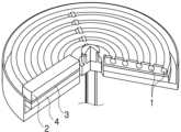
한편, 기판에 약액을 공급하여 처리하는 설비에서 처리 효율 향상을 위해 기판을 가열하면서 처리하는 경우가 있다.Meanwhile, in equipment that supplies a chemical solution to a substrate and processes it, there are cases where the substrate is heated while being processed to improve processing efficiency.
기판을 가열하기 위한 기판 가열 장치는 도 1에 도시된 바와 같이 열원인 램프히터(1), 반사판(3), 냉각 플레이트(4)를 포함할 수 있고, 램프히터(1)는 단자대(2)로부터 전력을 공급받는다. 공정이 완료된 이후에는 기판을 냉각할 필요가 있으므로 냉각 플레이트(4)에 의해 기판을 냉각한다.A substrate heating device for heating a substrate may include a lamp heater (1) as a heat source, a reflector (3), and a cooling plate (4) as shown in Fig. 1, and the lamp heater (1) is supplied with power from a terminal block (2). After the process is completed, the substrate needs to be cooled, so the substrate is cooled by a cooling plate (4).
그런데 상기 단자대(2)는 고온환경인 반사판(3)의 상부에 배치되므로 과열되어 수명이 단축될 수 있어서 적절한 냉각이 필요한데, 냉각 플레이트(4)의 상부에는 가열된 반사판이 있어서 단자대(2)의 냉각이 쉽지 않은 문제가 있다.However, since the terminal block (2) is placed on top of the reflector (3), which is in a high-temperature environment, it may overheat and shorten its lifespan, so proper cooling is required. However, there is a problem in that cooling of the terminal block (2) is not easy because there is a heated reflector on top of the cooling plate (4).
본 발명은 배경 기술의 문제점을 해결하기 위하여 안출된 것으로서, 본 발명이 해결하고자 하는 과제는 고온 환경에 노출된 단자대를 효율적으로 냉각할 수 있도록 구조가 개선된 기판 가열 장치 및 이를 이용한 기판 처리 장치를 제공하는 것이다.The present invention has been made to solve the problems of the background art, and the problem to be solved by the present invention is to provide a substrate heating device having an improved structure capable of efficiently cooling a terminal block exposed to a high temperature environment, and a substrate processing device using the same.
전술한 과제의 해결 수단으로서 본 발명은,As a means of solving the aforementioned problem, the present invention,
기판을 가열하기 위한 기판 가열 장치에 있어서,In a substrate heating device for heating a substrate,
상기 기판의 하부에 배치되는 열원인 가열부;A heating unit which is a heat source placed at the lower part of the above substrate;
상기 가열부의 아래쪽에 배치되어 냉기를 제공하는 냉각 플레이트;A cooling plate positioned below the heating section to provide cold air;
상기 가열부에 전력을 공급하며 하단부가 상기 냉각 플레이트와 접하는 단자대; 를 포함하는 것을 특징으로 하는 기판 가열 장치를 제공한다.A substrate heating device is provided, characterized by including a terminal block for supplying power to the heating unit and having a lower portion in contact with the cooling plate.
상기 가열부와 냉각 플레이트 사이에 배치되어 가열부에서 발산된 열을 기판 쪽으로 반사시키는 반사판;을 더 포함하는 것이 바람직하다.It is preferable to further include a reflection plate disposed between the heating unit and the cooling plate to reflect heat emitted from the heating unit toward the substrate.
상기 반사판에는 틈(opening)이 형성되어 있어서 상기 단자대의 하단부는 상기 틈을 관통한 상태로 상기 냉각 플레이트와 접하는 것이 바람직하다.It is preferable that an opening be formed in the above reflector so that the lower part of the terminal block penetrates the opening and comes into contact with the cooling plate.
상기 틈은 상기 단자대의 단면 형상에 대응하도록 구성되는 것이 바람직하다.It is preferable that the above gap be configured to correspond to the cross-sectional shape of the terminal block.
상기 냉각 플레이트에는 아래쪽으로 패인 홈이 마련되어 상기 단자대와 연결되는 전원 케이블은 상기 홈에 수용되어 냉각 플레이트에 의해 냉각되는 것이 바람직하다.It is preferable that the cooling plate has a groove formed downward, so that a power cable connected to the terminal block is received in the groove and cooled by the cooling plate.
상기 홈의 폭은 상기 틈의 폭에 비해 좁은 것이 바람직하다.It is preferable that the width of the above groove be narrower than the width of the gap.
상기 가열부는 동심원 형상의 여러 개의 IR 램프히터를 포함하며 각각의 IR 램프히터는 동일한 평면에 배치되는 것이 바람직하다.The above heating unit includes multiple IR lamp heaters in a concentric shape, and it is preferable that each IR lamp heater is arranged on the same plane.
상기 냉각 플레이트의 내부에는 냉각수가 흐르는 유로가 배치되는 것이 바람직하다.It is preferable that a flow path for cooling water be arranged inside the above cooling plate.
본 발명은 또한, 처리 영역을 제공하는 챔버;The present invention also comprises a chamber providing a processing area;
상기 챔버의 처리 영역에 설치되어 기판을 지지하는 기판 지지유닛;A substrate support unit installed in the processing area of the above chamber to support a substrate;
상기 기판 지지유닛에 의해 지지된 기판에 약액을 공급하기 위한 약액 공급유닛;A chemical solution supply unit for supplying a chemical solution to a substrate supported by the substrate support unit;
상기 기판을 가열하기 위한 기판 가열유닛; 을 포함하며,A substrate heating unit for heating the substrate;
상기 기판 가열유닛은 상기 기판의 하부에 배치되는 열원인 가열부와, 상기 가열부의 아래쪽에 배치되어 냉기를 제공하는 냉각 플레이트와, 상기 가열부에 전력을 공급하며 하단부가 상기 냉각 플레이트와 접하는 단자대를 포함하는 기판 처리 장치를 제공한다.The above substrate heating unit provides a substrate processing device including a heating unit which is a heat source and is arranged at the bottom of the substrate, a cooling plate which is arranged below the heating unit and provides cold air, and a terminal block which supplies power to the heating unit and has a lower portion in contact with the cooling plate.
또한, 본 발명은,In addition, the present invention,
기판의 표면을 식각하기 위한 기판 식각 장치에 있어서,In a substrate etching device for etching the surface of a substrate,
처리 영역을 제공하는 챔버;A chamber providing a processing area;
상기 챔버의 처리 영역에 설치되어 기판을 지지하며 스핀 척과 상기 스핀 척을 회전시키기 위한 회전 구동부를 포함하는 기판 지지유닛;A substrate support unit installed in the processing area of the chamber to support a substrate and including a spin chuck and a rotation driving unit for rotating the spin chuck;
상기 기판 지지유닛에 의해 지지된 기판에 식각액을 공급하기 위한 것으로서 상기 기판에 식각액을 분사하는 노즐, 상기 노즐을 이동시키기 위한 노즐 구동부, 상기 식각액을 가열하기 위한 식각액 가열부를 포함하는 식각액 공급유닛;An etchant supply unit for supplying an etchant to a substrate supported by the substrate support unit, the etchant supply unit including a nozzle for spraying an etchant onto the substrate, a nozzle driving unit for moving the nozzle, and an etchant heating unit for heating the etchant;
상기 식각액 공급유닛에 의해 기판의 표면으로 분사된 식각액이 기판의 표면과 반응하면서 생기는 반응 부산물이나 기판에서 비산된 식각액을 회수하기 위하여 상기 기판 지지유닛을 감싸는 형태로 마련되는 회수유닛;A recovery unit provided in a form that surrounds the substrate support unit to recover reaction by-products generated when the etchant sprayed onto the surface of the substrate by the etchant supply unit reacts with the surface of the substrate or etchant scattered from the substrate;
상기 기판을 가열하기 위하여 상기 스핀 척의 하부에 배치되는 기판 가열유닛; 을 포함하며,It includes a substrate heating unit positioned below the spin chuck to heat the substrate;
상기 기판 가열유닛은,The above substrate heating unit,
상기 지지유닛의 하부에 배치되는 열원으로서 여러 개가 동일한 평면에 동심원 형상으로 배치된 IR 램프히터인 가열부;A heating unit, which is a heat source arranged at the lower portion of the above support unit, and which is a plurality of IR lamp heaters arranged in a concentric shape on the same plane;
상기 가열부 하부에 배치되어 냉기를 제공하며 내부에 냉각수가 흐르는 유로가 형성된 냉각 플레이트;A cooling plate positioned below the heating section to provide cold air and having a passage formed inside through which cooling water flows;
상기 가열부에 전력을 공급하며 하단부가 상기 냉각 플레이트와 접하는 단자대;A terminal block that supplies power to the above heating unit and has a lower portion in contact with the cooling plate;
상기 가열부와 냉각 플레이트 사이에 배치되어 가열부에서 발산된 열을 기판 쪽으로 반사시키는 반사판을 포함하며,A reflector is included that is positioned between the heating unit and the cooling plate to reflect the heat emitted from the heating unit toward the substrate.
상기 반사판에는 상기 단자대의 단면 형상에 대응되는 형상의 틈(opening)이 형성되어 있어서 상기 단자대의 하단부는 상기 틈을 관통한 상태로 상기 냉각 플레이트와 접하고,The above reflector has a gap (opening) formed in a shape corresponding to the cross-sectional shape of the terminal block, so that the lower part of the terminal block comes into contact with the cooling plate while penetrating the gap.
상기 냉각 플레이트 중 상기 틈의 하부에는 아래쪽으로 상기 틈의 폭에 비해 좁은 폭을 가지도록 패인 홈이 마련되어 상기 단자대와 연결되는 전원 케이블은 상기 홈에 수용되어 냉각 플레이트에 의해 냉각되는 기판 식각 장치를 제공한다.A groove is provided at the lower portion of the gap among the cooling plates so as to have a width narrower than the width of the gap, and a power cable connected to the terminal block is received in the groove to provide a substrate etching device cooled by the cooling plate.
본 발명에 의하면 고온 환경에 노출된 단자대를 효율적으로 냉각할 수 있도록 구조가 개선된 기판 가열 장치 및 이를 이용한 기판 처리 장치를 제공할 수 있다.According to the present invention, a substrate heating device having an improved structure capable of efficiently cooling a terminal block exposed to a high-temperature environment and a substrate processing device using the same can be provided.
도 1은 종래의 기판 가열 장치를 설명하기 위한 단면도.
도 2는 본 발명의 하나의 실시예에 따른 기판 가열 장치의 분리 사시도.
도 3은 도 2에 도시된 기판 가열 장치의 결합단면도.
도 4는 본 발명의 하나의 실시예에 따른 기판 처리 장치를 설명하기 위한 도면.
도 5는 본 발명의 하나의 실시예에 따른 기판 식각 장치를 설명하기 위한 도면.Fig. 1 is a cross-sectional view illustrating a conventional substrate heating device.
FIG. 2 is an exploded perspective view of a substrate heating device according to one embodiment of the present invention.
Fig. 3 is a cross-sectional view of the substrate heating device illustrated in Fig. 2.
FIG. 4 is a drawing for explaining a substrate processing device according to one embodiment of the present invention.
FIG. 5 is a drawing for explaining a substrate etching device according to one embodiment of the present invention.
이하에서는 도면을 참조하면서 본 발명의 바람직한 실시예에 대하여 설명함으로써 본 발명을 실시하기 위한 구체적인 내용을 제공하기로 한다.Hereinafter, specific details for carrying out the present invention will be provided by describing preferred embodiments of the present invention with reference to the drawings.
우선 본 발명의 첫 번째 형태인 기판 가열 장치에 대하여 설명하기로 한다.First, the substrate heating device, which is the first form of the present invention, will be described.
도 2는 본 발명의 하나의 실시예에 따른 기판 가열 장치의 분리 사시도이고, 도 3은 도 2에 도시된 기판 가열 장치의 결합단면도이다.FIG. 2 is an exploded perspective view of a substrate heating device according to one embodiment of the present invention, and FIG. 3 is a cross-sectional view of the substrate heating device illustrated in FIG. 2.
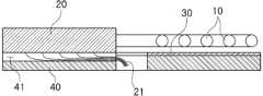
본 실시예에 따른 기판 가열 장치(100)는 식각이나 세정 등의 처리를 위한 기판 처리 장치에 설치되어 기판(W)을 가열하는 장치로서 가열부(10), 단자대(20), 반사판(30) 및 냉각 플레이트(40)를 포함하여 구성된다.The substrate heating device (100) according to the present embodiment is a device installed in a substrate processing device for processing such as etching or cleaning and heats a substrate (W), and is configured to include a heating unit (10), a terminal block (20), a reflector (30), and a cooling plate (40).
상기 가열부(10)는 기판(W)을 가열하기 위하여 상기 기판(W)의 하부에 배치되는 열원이다. 상기 기판(W)은 스핀 척(50)에 의해 지지가 되는데 스핀 척(50)에는 기판(W)과 접하면서 지지하는 여러 개의 척 핀(51)이 설치된다.The above heating unit (10) is a heat source placed at the bottom of the substrate (W) to heat the substrate (W). The substrate (W) is supported by a spin chuck (50), and several chuck pins (51) are installed on the spin chuck (50) to support the substrate (W) while making contact with it.
상기 가열부(10)는 도 2에 도시된 바와 같이 여러 개가 동심원 형상으로 배치되는 IR 램프히터로 구성될 수 있다. 각각의 IR 램프히터는 내부가 빈 케이싱과 케이싱의 내부에 설치되는 필라멘트(미도시)를 포함하며, 케이싱의 양단부는 발열을 위한 전력공급을 받기 위해 단자대(20)와 연결된다.The above heating unit (10) may be composed of a plurality of IR lamp heaters arranged in a concentric shape as shown in Fig. 2. Each IR lamp heater includes an internally empty casing and a filament (not shown) installed inside the casing, and both ends of the casing are connected to a terminal block (20) to receive power for heat generation.
상기 여러 개의 IR 램프히터는 동일한 평면에 배치되는데, IR 램프히터가 동일한 평면에 배치된다는 의미는 각각의 IR 램프히터가 설치된 높이가 모두 같아서 각각의 IR 램프히터와 기판(W) 사이의 거리가 동일하다는 의미이다. 기판을 처리하는 과정에서 기판(W)을 균일하게 가열하지 않으면 기판의 처리 균일도가 떨어질 수 있는데, IR 램프히터를 동일한 평면에 배치하면 각각의 IR 램프히터와 기판(W) 사이의 거리가 동일해져서 기판(W)을 균일하게 가열할 수 있다. 상기 가열부(10)인 IR 램프히터에는 중력에 의해 아래로 처지는 것을 방지하여 동일한 평면에 배치되는 것이 유지될 수 있도록 IR 램프히터를 지지하는 지지수단(11)이 마련된다.The above multiple IR lamp heaters are arranged on the same plane. That the IR lamp heaters are arranged on the same plane means that the heights at which each IR lamp heater is installed are all the same, so that the distance between each IR lamp heater and the substrate (W) is the same. If the substrate (W) is not heated uniformly during the process of processing the substrate, the uniformity of the processing of the substrate may deteriorate. However, if the IR lamp heaters are arranged on the same plane, the distance between each IR lamp heater and the substrate (W) becomes the same, so that the substrate (W) can be heated uniformly. The IR lamp heater, which is the heating unit (10), is provided with a support means (11) to support the IR lamp heater so that it can be maintained so as to prevent it from sagging due to gravity and to be arranged on the same plane.
상기 단자대(20)는 전원으로부터 전력을 공급받아 상기 가열부(10)에 공급하는 구성으로서 전력 공급을 위한 전원 케이블(21)과 연결된다. 상기 단자대(20)는 세라믹 재질로 제작될 수 있다.The terminal block (20) above is configured to receive power from a power source and supply it to the heating unit (10) and is connected to a power cable (21) for power supply. The terminal block (20) above can be made of a ceramic material.
상기 반사판(30)은 상기 기판(W)을 효율적으로 가열하기 위하여 상기 가열부(10)의 아래쪽에 배치되어 가열부(10)인 IR 램프히터에서 발산된 열을 기판(W) 쪽으로 반사시킨다. 또한, 반사판(30)은 기판(W)을 균일하게 가열할 수 있게 한다.The above reflector (30) is placed below the heating unit (10) to efficiently heat the substrate (W) and reflects the heat emitted from the IR lamp heater, which is the heating unit (10), toward the substrate (W). In addition, the reflector (30) enables the substrate (W) to be heated evenly.
상기 반사판(30)은 상기 발열수단(10)에서 발산된 복사열이 투과되지 못하도록 불투명한 재질로 제작될 수 있다.The above reflector (30) can be made of an opaque material to prevent the radiant heat emitted from the heating means (10) from penetrating.
상기 반사판(30)에는 도 2에 도시된 바와 같이 상기 단자대(20)의 단면 형상에 대응되는 형상의 틈(31; opening)이 형성된다. 상기 단자대(20)의 단면 형상에 대응되는 형상이란 상기 단자대(20)가 상기 틈(31)을 관통하도록 배치될 때 틈(31) 중 단자대(20)가 관통하고 남은 공간이 제작 공차 정도로 적은 형상을 의미한다. 틈(31)의 형상을 단자대(20)의 단면 형상과 대응되는 형상으로 구성함으로써 반사판(30)의 면적을 최대화하여 가열부(10)에서 발산된 열을 최대한으로 반사시킬 수 있도록 구성한다.As shown in Fig. 2, a gap (31; opening) having a shape corresponding to the cross-sectional shape of the terminal block (20) is formed in the reflector (30). The shape corresponding to the cross-sectional shape of the terminal block (20) means a shape in which, when the terminal block (20) is arranged to penetrate the gap (31), the remaining space in the gap (31) is as small as the manufacturing tolerance. By configuring the shape of the gap (31) to correspond to the cross-sectional shape of the terminal block (20), the area of the reflector (30) is maximized so that the heat emitted from the heating unit (10) can be reflected to the greatest extent possible.
상기 냉각 플레이트(40)는 상기 반사판(30)의 하부에 배치되어 냉기를 제공하는 구성으로서 내부에는 냉각수가 흐르는 유로(미도시)가 배치되어 냉각수가 유로를 따라 흐르도록 구성된다. 냉각 플레이트(40)에 배치된 유로를 따라 냉각수가 흐르면서 열을 흡수하여 외부로 배출된다.The cooling plate (40) is arranged at the bottom of the reflector (30) to provide cold air, and is configured to have a channel (not shown) for cooling water flowing inside so that the cooling water flows along the channel. As the cooling water flows along the channel arranged in the cooling plate (40), it absorbs heat and discharges it to the outside.
상기 냉각 플레이트(40)는 기판(W), 단자대(20) 및 하부 척(60)을 냉각시킬 수 있도록 하부 척(60)의 상부에 배치되며, 하부 척(60)에 의해 지지된다.The above cooling plate (40) is placed on top of the lower chuck (60) so as to cool the substrate (W), terminal block (20), and lower chuck (60), and is supported by the lower chuck (60).
상기 단자대(20)의 하단부는 상기 틈(31)을 관통하여 상기 냉각 플레이트(40)와 직접 접촉하도록 구성된다. 단자대(20)가 냉각 플레이트(40)와 직접 접촉함으로써 단자대(20)의 냉각효율을 높여 가열부(10)에 의해 기판(W)을 가열하는 과정에서 단자대(20)가 함께 과열되어 손상되는 것을 방지한다.The lower part of the terminal block (20) is configured to penetrate the gap (31) and make direct contact with the cooling plate (40). By making direct contact with the cooling plate (40), the terminal block (20) increases the cooling efficiency of the terminal block (20), thereby preventing the terminal block (20) from being overheated and damaged during the process of heating the substrate (W) by the heating unit (10).
도 3에 도시된 바와 같이 상기 냉각 플레이트(40) 중 상기 틈(31)의 하부에는 아래 쪽으로 패인 홈(41)이 형성되고, 중앙부에는 관통공(42)이 형성되어 있다. 상기 단자대(20)와 연결되는 전원 케이블(21)이 상기 홈(41)에 수용된 상태로 냉각 플레이트(40)에 의해 냉각되고 상기 관통공(42)을 관통하도록 구성되어 있어서 전원 케이블(21)의 냉각효율을 높일 수 있도록 한다.As shown in Fig. 3, a groove (41) is formed downwardly at the bottom of the gap (31) of the cooling plate (40), and a through hole (42) is formed in the center. The power cable (21) connected to the terminal block (20) is cooled by the cooling plate (40) while being accommodated in the groove (41) and is configured to pass through the through hole (42), thereby increasing the cooling efficiency of the power cable (21).
상기 단자대(20)와 마찬가지로 단자대(20)와 연결된 전원 케이블(21) 역시 가열부(10)에 의해 가열되어 수명이 짧아지거나 효율이 떨어질 수 있는데 홈(41)에 수용된 상태로 냉각될 수 있도록 함으로써 전원 케이블(21)이 가열됨에 따라 발생할 수 있는 문제를 해결한다.As with the above terminal block (20), the power cable (21) connected to the terminal block (20) may also be heated by the heating unit (10), which may shorten its lifespan or reduce its efficiency. However, by allowing it to be cooled while being accommodated in the groove (41), problems that may occur as the power cable (21) is heated are solved.
전원 케이블(21)은 홈(41) 내에서 냉각 플레이트(40)에 직접 접촉함으로써 냉각 플레이트(40)에 의해 냉각될 수 있다.The power cable (21) can be cooled by the cooling plate (40) by directly contacting the cooling plate (40) within the groove (41).
한편, 상기 홈(41)의 폭(d1)은 상기 틈(31)의 폭(d2)에 비해 작게 형성되어 상기 단자대(30)가 냉각 플레이트(40)에 지지될 수 있도록 구성할 수 있다.Meanwhile, the width (d1) of the groove (41) can be formed smaller than the width (d2) of the gap (31) so that the terminal block (30) can be supported on the cooling plate (40).
상기 반사판(30)과 하부 척(60)에도 상기 냉각 플레이트(40)와 마찬가지로 각각 관통공(32, 61)이 형성되어 있는데 이는 스핀 척(50)을 회전시키기 위한 회전 구동부(미도시)의 회전축인 스핀들(미도시)을 설치하기 위한 공간이 필요하기 때문이다.The above reflector (30) and lower chuck (60) also have through holes (32, 61) formed therein, just like the cooling plate (40). This is because space is needed to install a spindle (not shown), which is a rotational axis of a rotational driving unit (not shown) for rotating the spin chuck (50).
이하에서는 본 발명의 두 번째 형태인 기판 처리 장치의 일 실시예에 대하여 설명하기로 한다.Below, one embodiment of a substrate processing device, which is the second form of the present invention, will be described.
도 4는 본 발명의 하나의 실시예에 따른 기판 처리 장치를 설명하기 위한 도면이다.FIG. 4 is a drawing for explaining a substrate processing device according to one embodiment of the present invention.
본 실시예에 따른 기판 처리 장치는 챔버(1000), 기판 지지유닛(200), 약액 공급유닛(300), 기판 가열유닛(100)을 포함하여 구성된다. 본 실시예의 기판 처리 장치는 기판을 세정하기 위한 세정 장치나 식각 장치 등 기판을 가열하면서 공정을 수행하는 다양한 종류의 장치일 수 있다.The substrate processing device according to the present embodiment is configured to include a chamber (1000), a substrate support unit (200), a chemical supply unit (300), and a substrate heating unit (100). The substrate processing device according to the present embodiment may be various types of devices that perform a process while heating a substrate, such as a cleaning device for cleaning a substrate or an etching device.
상기 챔버(1000)는 기판을 처리하기 위한 처리 영역을 제공한다.The above chamber (1000) provides a processing area for processing a substrate.
상기 기판 지지유닛(200)은 상기 챔버(1000)가 제공하는 처리 영역에 설치되어 기판(W)을 지지하는 구성으로서 스핀 척(50), 하부 척(60), 스핀들(70) 및 회전구동부(80)를 포함하여 구성될 수 있다. 상기 스핀 척(50)에는 여러 개의 척 핀(51)이 설치된다.The above substrate support unit (200) is installed in the processing area provided by the chamber (1000) and is configured to support the substrate (W), and may include a spin chuck (50), a lower chuck (60), a spindle (70), and a rotation driving unit (80). A plurality of chuck pins (51) are installed in the spin chuck (50).
상기 기판 지지유닛(200)의 주변에는 기판(W)의 표면으로 분사되어 기판(W)을 처리한 후 생기는 처리 부산물이나 기판(W)에서 비산된 약액을 회수하기 위한 회수유닛(500)이 마련될 수 있다.A recovery unit (500) may be provided around the substrate support unit (200) to recover treatment by-products generated after spraying onto the surface of the substrate (W) and treating the substrate (W) or the chemical liquid flying from the substrate (W).
상기 약액 공급유닛(300)은 상기 기판(W)을 처리하기 위한 약액을 공급하기 위한 구성으로서 배관과 밸브, 펌프 등을 포함하여 구성될 수 있는데 이는 공지의 구성을 적용할 수 있으므로 상세한 설명은 생략한다. 도면에 점선은 약액의 이동을 표시한 것이다. 상기 약액으로는 기판(W)을 세정하기 위한 세정액이나 기판(W)을 식각하기 위한 식각액 등이 될 수 있다.The above-mentioned chemical supply unit (300) is configured to supply a chemical for processing the substrate (W) and may include a pipe, a valve, a pump, etc., and since a known configuration can be applied, a detailed description thereof will be omitted. The dotted line in the drawing indicates the movement of the chemical. The chemical may be a cleaning solution for cleaning the substrate (W) or an etching solution for etching the substrate (W).
상기 약액 공급유닛(300)은 분사 유닛(400)을 포함할 수 있는데, 상기 분사 유닛(400)은 약액 공급유닛(300)과 연결되어 약액 공급유닛(300)에 의해 공급된 약액을 기판(W)에 분사하는 구성이다. 상기 분사 유닛(400)은 노즐 헤드(401)와 노즐(402)을 포함하여 구성될 수 있으며, 노즐(402)을 통해 기판(W)으로 약액을 분사한다.The above-mentioned liquid supply unit (300) may include a spray unit (400), and the spray unit (400) is configured to be connected to the liquid supply unit (300) and spray the liquid supplied by the liquid supply unit (300) onto the substrate (W). The spray unit (400) may include a nozzle head (401) and a nozzle (402), and sprays the liquid onto the substrate (W) through the nozzle (402).
상기 기판 가열유닛(100)은 상기 기판(W)을 가열하는 구성으로서, 가열부(10), 단자대(20), 반사판(30) 및 냉각 플레이트(40)를 포함하여 구성되는데(도 2 및 도 3 참조), 전술한 기판 가열장치와 실질적으로 동일한 구성으로 볼 수 있으며 앞서 설명하였으므로 추가적인 설명은 생략하기로 한다.The above substrate heating unit (100) is configured to heat the substrate (W) and includes a heating unit (10), a terminal block (20), a reflector (30), and a cooling plate (40) (see FIGS. 2 and 3). It can be viewed as having substantially the same configuration as the above-described substrate heating device, and as it has been described above, further description will be omitted.
이하에서는 도면을 참조하면서 본 발명의 세 번째 형태인 기판 식각 장치의 일 실시예에 대하여 설명하기로 한다.Hereinafter, an embodiment of a substrate etching device, which is a third form of the present invention, will be described with reference to the drawings.
도 5는 본 발명의 하나의 실시예에 따른 기판 식각 장치를 설명하기 위한 도면이다.FIG. 5 is a drawing for explaining a substrate etching device according to one embodiment of the present invention.
본 실시예에 따른 기판 식각 장치는 기판(W)의 표면을 식각하기 위한 장치로서 챔버(1000), 기판 지지유닛(200), 식각액 공급유닛(300), 회수유닛(500) 및 기판 가열유닛(100)을 포함하여 이루어진다.The substrate etching device according to the present embodiment is a device for etching the surface of a substrate (W) and comprises a chamber (1000), a substrate support unit (200), an etchant supply unit (300), a recovery unit (500), and a substrate heating unit (100).
상기 챔버(1000)는 식각 처리를 위한 처리 영역을 제공한다.The above chamber (1000) provides a processing area for etching treatment.
상기 기판 지지유닛(200)은 상기 챔버(1000)가 제공하는 영역에 설치되어 기판(W)을 지지하는 구성으로서 스핀 척(50), 하부 척(60), 스핀들(70), 회전 구동부(80)를 포함하여 구성될 수 있다. 상기 스핀 척(50)에는 여러 개의 척 핀(51)이 설치된다.The above substrate support unit (200) is configured to be installed in an area provided by the chamber (1000) and support a substrate (W), and may include a spin chuck (50), a lower chuck (60), a spindle (70), and a rotation driving unit (80). A plurality of chuck pins (51) are installed in the spin chuck (50).
상기 식각액 공급유닛(300)은 상기 기판 지지유닛(200)에 의해 지지된 기판(W)에 식각액을 공급하기 위한 구성으로서 노즐(301), 노즐 구동부(302), 식각액 가열부(303)를 포함하여 구성될 수 있다. 상기 식각액으로는 인산(H3PO4)이 사용될 수 있으며, 인산에 의해 기판(W) 표면의 실리콘 산화막이나 실리콘 질화막 등을 식각 할 수 있다.The above etchant supply unit (300) is configured to supply an etchant to a substrate (W) supported by the substrate support unit (200), and may include a nozzle (301), a nozzle driving unit (302), and an etchant heating unit (303). Phosphoric acid (H3 PO4 ) may be used as the etchant, and a silicon oxide film or a silicon nitride film on the surface of the substrate (W) may be etched by the phosphoric acid.
상기 노즐(301)은 식각액을 기판(W)에 직접 분사하는 구성이다.The above nozzle (301) is configured to directly spray the etchant onto the substrate (W).
상기 노즐 구동부(302)는 상기 노즐(301)을 이동시키는 구성으로서, 노즐(301)이 기판(W)에 식각액을 분사할 때에는 노즐(301)이 기판(W)의 중심 상부에 위치할 수 있도록 구동하고, 식각액 분사가 완료된 후에는 노즐(301)이 기판으로부터 이격되도록 구동한다.The above nozzle driving unit (302) is configured to move the nozzle (301), and when the nozzle (301) sprays the etchant onto the substrate (W), it drives the nozzle (301) so that it can be positioned at the upper center of the substrate (W), and after the etchant spraying is completed, it drives the nozzle (301) so that it is separated from the substrate.
상기 식각액 가열부(303)는 식각액을 가열한다. 식각액에 의한 식각은 화학반응에 의해 이루어지는데 식각액의 온도가 올라가면 화학반응의 속도가 증가할 수 있으므로 식각액을 가열하는 것이다. 식각액 가열부(303)는 식각액을 끓는 점 이하의 온도, 예를 들어 150℃로 가열할 수 있다.The above etchant heating unit (303) heats the etchant. Etching by the etchant is performed by a chemical reaction, and since the speed of the chemical reaction can increase when the temperature of the etchant increases, the etchant is heated. The etchant heating unit (303) can heat the etchant to a temperature below the boiling point, for example, 150°C.
한편, 식각 반응을 위해 식각액과 함께 기판(W)에 순수(Deionized water; DIW)를 공급하는 순수 공급유닛(400)이 포함될 수도 있다. 순수 공급유닛(400)은 순수노즐(401), 순수노즐 구동부(미도시), 순수 가열부(402)를 포함할 수 있다.Meanwhile, a pure water supply unit (400) that supplies pure water (deionized water; DIW) to the substrate (W) together with the etchant for the etching reaction may be included. The pure water supply unit (400) may include a pure water nozzle (401), a pure water nozzle driving unit (not shown), and a pure water heating unit (402).
상기 순수노즐(401)은 기판(W)에 순수를 분사하는 구성이고, 순수노줄 구동부는 상기 순수노즐(401)을 구동하는 구성이며, 순수 가열부(402)는 식각 반응 속도를 올리기 위해 순수를 가열하는 구성이다. 상기 순수노즐 구동부의 구동 메커니즘은 상기 노즐 구동부(302)의 구동 메커니즘과 실질적으로 동일하게 구성될 수 있다.The above pure water nozzle (401) is configured to spray pure water onto the substrate (W), the pure water nozzle drive unit is configured to drive the pure water nozzle (401), and the pure water heating unit (402) is configured to heat the pure water to increase the etching reaction speed. The driving mechanism of the above pure water nozzle drive unit can be configured to be substantially the same as the driving mechanism of the above nozzle drive unit (302).
상기 회수유닛(500)은 상기 식각액 공급유닛(300)에 의해 기판(W)의 표면으로 분사된 식각액이나 순수가 기판의 표면과 반응하면서 생기는 반응 부산물이나 기판(W)에서 비산된 식각액이나 순수를 회수하는 구성으로서 도 5에 도시된 바와 같이 기판 지지유닛(200)과 기판(W)을 감싸는 형태로 배치된다.The above recovery unit (500) is configured to recover reaction by-products generated when the etchant or pure water sprayed onto the surface of the substrate (W) by the etchant supply unit (300) reacts with the surface of the substrate, or etchant or pure water scattered from the substrate (W), and is arranged in a form that surrounds the substrate support unit (200) and the substrate (W), as illustrated in FIG. 5.
상기 기판 가열유닛(100)은 상기 기판(W)을 가열하기 위하여 상기 스핀 척(50)의 하부에 배치되는 구성으로서, 가열부(10), 단자대(20), 반사판(30) 및 냉각 플레이트(40)를 포함하여 구성되는데(도 2 또는 도 3 참조), 전술한 기판 가열장치와 실질적으로 동일한 구성이므로 추가적인 설명은 생략하기로 한다.The above substrate heating unit (100) is configured to be placed below the spin chuck (50) to heat the substrate (W), and includes a heating unit (10), a terminal block (20), a reflector (30), and a cooling plate (40) (see FIG. 2 or FIG. 3). Since it has substantially the same configuration as the substrate heating device described above, further description will be omitted.
이상에서 본 발명의 바람직한 실시예에 대하여 설명함으로써 본 발명을 실시하기 위한 구체적인 내용을 제공하였으나 본 발명의 기술적 사상이 설명된 실시예에 한정되는 것은 아니며 본 발명의 기술적 사상에 어긋나지 않는 범위 안에서 다양한 형태로 구체화될 수 있다.Although the preferred embodiments of the present invention have been described above to provide specific details for carrying out the present invention, the technical idea of the present invention is not limited to the described embodiments and may be embodied in various forms within a scope that does not deviate from the technical idea of the present invention.
10 : 가열부20 : 단자대
30 : 반사판40 : 냉각 플레이트10: Heating section 20: Terminal block
30 : Reflector 40 : Cooling Plate
Claims (20)
Translated fromKorean상기 기판의 하부에 배치되는 열원인 가열부;
상기 가열부의 아래쪽에 배치되어 냉기를 제공하는 냉각 플레이트;
상기 가열부에 전력을 공급하며 하단부가 상기 냉각 플레이트와 접하는 단자대; 및
상기 가열부와 냉각 플레이트 사이에 배치되어 가열부에서 발산된 열을 기판 쪽으로 반사시키는 반사판;
을 포함하고,
상기 반사판에는 틈(opening)이 형성되어 있어서 상기 단자대의 하단부는 상기 틈을 관통한 상태로 상기 냉각 플레이트와 접하는 것을 특징으로 하는 기판 가열 장치.
In a substrate heating device for heating a substrate,
A heating unit which is a heat source placed at the lower part of the above substrate;
A cooling plate positioned below the heating section to provide cold air;
A terminal block that supplies power to the heating unit and has a lower portion in contact with the cooling plate; and
A reflector disposed between the heating unit and the cooling plate to reflect heat emitted from the heating unit toward the substrate;
Including,
A substrate heating device characterized in that a gap (opening) is formed in the above reflector so that the lower part of the terminal block penetrates the gap and comes into contact with the cooling plate.
상기 틈은 상기 단자대의 단면 형상에 대응하도록 구성되는 기판 가열 장치.
In the first paragraph,
A substrate heating device in which the above gap is configured to correspond to the cross-sectional shape of the terminal block.
상기 냉각 플레이트에는 아래쪽으로 패인 홈이 마련되어 상기 단자대와 연결되는 전원 케이블은 상기 홈에 수용되어 냉각 플레이트에 의해 냉각되는 기판 가열 장치.
In the first paragraph,
A substrate heating device in which a groove is formed downward on the cooling plate, and a power cable connected to the terminal block is received in the groove and cooled by the cooling plate.
상기 홈은 상기 틈의 하부에 마련되는 기판 가열 장치.
In paragraph 5,
The above home is a substrate heating device provided at the lower part of the above gap.
상기 홈의 폭은 상기 틈의 폭에 비해 좁은 기판 가열 장치.
In Article 6,
A substrate heating device in which the width of the above groove is narrower than the width of the above gap.
상기 가열부는 동심원 형상의 여러 개의 IR 램프히터를 포함하며 각각의 IR 램프히터는 동일한 평면에 배치되는 기판 가열 장치.
In the first paragraph,
The above heating unit is a substrate heating device including multiple IR lamp heaters in a concentric shape, each IR lamp heater being arranged on the same plane.
상기 냉각 플레이트의 내부에는 냉각수가 흐르는 유로가 배치되는 기판 가열 장치.
In the first paragraph,
A substrate heating device having a cooling water flow path arranged inside the cooling plate.
상기 챔버의 처리 영역에 설치되어 기판을 지지하는 기판 지지유닛;
상기 기판 지지유닛에 의해 지지된 기판에 약액을 공급하기 위한 약액 공급유닛;
상기 기판을 가열하기 위한 기판 가열유닛; 을 포함하며,
상기 기판 가열유닛은 상기 기판의 하부에 배치되는 열원인 가열부와, 상기 가열부의 아래쪽에 배치되어 냉기를 제공하는 냉각 플레이트와, 상기 가열부에 전력을 공급하며 하단부가 상기 냉각 플레이트와 접하는 단자대와, 상기 가열부와 냉각 플레이트 사이에 배치되어 가열부에서 발산된 열을 기판 쪽으로 반사시키는 반사판을 포함하고,
상기 반사판에는 틈(opening)이 형성되어 있어서 상기 단자대의 하단부는 상기 틈을 관통한 상태로 상기 냉각 플레이트와 접촉하는 기판 처리 장치.
A chamber providing a processing area;
A substrate support unit installed in the processing area of the above chamber to support a substrate;
A chemical solution supply unit for supplying a chemical solution to a substrate supported by the substrate support unit;
A substrate heating unit for heating the substrate;
The above substrate heating unit includes a heating unit which is a heat source and is arranged at the bottom of the substrate, a cooling plate which is arranged below the heating unit and provides cold air, a terminal block which supplies power to the heating unit and has a lower portion in contact with the cooling plate, and a reflection plate which is arranged between the heating unit and the cooling plate and reflects the heat emitted from the heating unit toward the substrate.
A substrate processing device in which a gap (opening) is formed in the above reflector so that the lower part of the terminal block penetrates the gap and comes into contact with the cooling plate.
상기 틈은 상기 단자대의 단면 형상에 대응하도록 구성되는 기판 처리 장치.
In Article 10,
A substrate processing device in which the above gap is configured to correspond to the cross-sectional shape of the terminal block.
상기 냉각 플레이트에는 아래쪽으로 패인 홈이 마련되어 상기 단자대와 연결되는 전원 케이블은 상기 홈에 수용되어 냉각 플레이트에 의해 냉각되는 기판 처리 장치.
In Article 10,
A substrate processing device in which a groove is formed downward on the cooling plate, and a power cable connected to the terminal block is received in the groove and cooled by the cooling plate.
상기 홈은 상기 틈의 하부에 마련되는 기판 처리 장치.
In Article 14,
The above home is a substrate processing device provided at the bottom of the above gap.
상기 홈의 폭은 상기 틈의 폭에 비해 좁은 기판 처리 장치.
In Article 15,
A substrate processing device in which the width of the above groove is narrower than the width of the above gap.
상기 가열부는 동심원 형상의 여러 개의 IR 램프히터를 포함하며 각각의 IR 램프히터는 동일한 평면에 배치되는 기판 처리 장치.
In Article 16,
A substrate processing device in which the above heating unit includes multiple IR lamp heaters in a concentric shape, each IR lamp heater being arranged on the same plane.
상기 냉각 플레이트의 내부에는 냉각수가 흐르는 유로가 배치되는 기판 처리 장치.
In Article 10,
A substrate processing device in which a cooling water flow path is arranged inside the above cooling plate.
상기 기판 지지유닛은 스핀 척과 상기 스핀 척의 아래쪽에 배치되어 상기 스핀 척을 회전시키기 위한 회전 구동부를 포함하는 기판 처리 장치.
In Article 10,
A substrate processing device wherein the substrate support unit includes a spin chuck and a rotation driving unit positioned below the spin chuck to rotate the spin chuck.
처리 영역을 제공하는 챔버;
상기 챔버의 처리 영역에 설치되어 기판을 지지하며 스핀 척과 상기 스핀 척을 회전시키기 위한 회전 구동부를 포함하는 기판 지지유닛;
상기 기판 지지유닛에 의해 지지된 기판에 식각액을 공급하기 위한 것으로서 상기 기판에 식각액을 분사하는 노즐, 상기 노즐을 이동시키기 위한 노즐 구동부, 상기 식각액을 가열하기 위한 식각액 가열부를 포함하는 식각액 공급유닛;
상기 식각액 공급유닛에 의해 기판의 표면으로 분사된 식각액이 기판의 표면과 반응하면서 생기는 반응 부산물이나 기판에서 비산된 식각액을 회수하기 위하여 상기 기판 지지유닛을 감싸는 형태로 마련되는 회수유닛;
상기 기판을 가열하기 위하여 상기 스핀 척의 하부에 배치되는 기판 가열유닛; 을 포함하며,
상기 기판 가열유닛은,
상기 지지유닛의 하부에 배치되는 열원으로서 여러 개가 동일한 평면에 동심원 형상으로 배치된 IR 램프히터인 가열부;
상기 가열부 하부에 배치되어 냉기를 제공하며 내부에 냉각수가 흐르는 유로가 형성된 냉각 플레이트;
상기 가열부에 전력을 공급하며 하단부가 상기 냉각 플레이트와 접하는 단자대;
상기 가열부와 냉각 플레이트 사이에 배치되어 가열부에서 발산된 열을 기판 쪽으로 반사시키는 반사판을 포함하며,
상기 반사판에는 상기 단자대의 단면 형상에 대응되는 형상의 틈(opening)이 형성되어 있어서 상기 단자대의 하단부는 상기 틈을 관통한 상태로 상기 냉각 플레이트와 접하고,
상기 냉각 플레이트 중 상기 틈의 하부에는 아래쪽으로 상기 틈의 폭에 비해 좁은 폭을 가지도록 패인 홈이 마련되어 상기 단자대와 연결되는 전원 케이블은 상기 홈에 수용되어 냉각 플레이트에 의해 냉각되는 기판 식각 장치.
In a substrate etching device for etching the surface of a substrate,
A chamber providing a processing area;
A substrate support unit installed in the processing area of the chamber to support a substrate and including a spin chuck and a rotation driving unit for rotating the spin chuck;
An etchant supply unit for supplying an etchant to a substrate supported by the substrate support unit, the etchant supply unit including a nozzle for spraying an etchant onto the substrate, a nozzle driving unit for moving the nozzle, and an etchant heating unit for heating the etchant;
A recovery unit provided in a form that surrounds the substrate support unit to recover reaction by-products generated when the etchant sprayed onto the surface of the substrate by the etchant supply unit reacts with the surface of the substrate or etchant scattered from the substrate;
It includes a substrate heating unit positioned below the spin chuck to heat the substrate;
The above substrate heating unit,
A heating unit, which is a heat source arranged at the lower portion of the above support unit, and which is a plurality of IR lamp heaters arranged in a concentric shape on the same plane;
A cooling plate positioned below the heating section to provide cold air and having a passage formed inside through which cooling water flows;
A terminal block that supplies power to the above heating unit and has a lower portion in contact with the cooling plate;
A reflector is included that is positioned between the heating unit and the cooling plate to reflect the heat emitted from the heating unit toward the substrate.
The above reflector has a gap (opening) formed in a shape corresponding to the cross-sectional shape of the terminal block, so that the lower part of the terminal block comes into contact with the cooling plate while penetrating the gap.
A substrate etching device in which a groove is formed at the lower portion of the gap among the cooling plates so as to have a width narrower than the width of the gap, and a power cable connected to the terminal block is received in the groove and cooled by the cooling plate.
Priority Applications (4)
| Application Number | Priority Date | Filing Date | Title |
|---|---|---|---|
| KR1020220116952AKR102776629B1 (en) | 2022-09-16 | 2022-09-16 | Wafer Heating Apparatus and Wafer Processing Apparatus using above |
| JP2022189008AJP7422847B1 (en) | 2022-09-16 | 2022-11-28 | Substrate heating device and substrate processing device using the same |
| CN202310303666.3ACN117727652A (en) | 2022-09-16 | 2023-03-27 | Substrate heating apparatus and substrate processing apparatus using the same |
| US18/126,933US20240096663A1 (en) | 2022-09-16 | 2023-03-27 | Wafer heating apparatus and wafer processing apparatus using the same |
Applications Claiming Priority (1)
| Application Number | Priority Date | Filing Date | Title |
|---|---|---|---|
| KR1020220116952AKR102776629B1 (en) | 2022-09-16 | 2022-09-16 | Wafer Heating Apparatus and Wafer Processing Apparatus using above |
Publications (2)
| Publication Number | Publication Date |
|---|---|
| KR20240038856A KR20240038856A (en) | 2024-03-26 |
| KR102776629B1true KR102776629B1 (en) | 2025-03-07 |
Family
ID=89620898
Family Applications (1)
| Application Number | Title | Priority Date | Filing Date |
|---|---|---|---|
| KR1020220116952AActiveKR102776629B1 (en) | 2022-09-16 | 2022-09-16 | Wafer Heating Apparatus and Wafer Processing Apparatus using above |
Country Status (4)
| Country | Link |
|---|---|
| US (1) | US20240096663A1 (en) |
| JP (1) | JP7422847B1 (en) |
| KR (1) | KR102776629B1 (en) |
| CN (1) | CN117727652A (en) |
Families Citing this family (1)
| Publication number | Priority date | Publication date | Assignee | Title |
|---|---|---|---|---|
| JP7625458B2 (en)* | 2021-03-22 | 2025-02-03 | 株式会社Screenホールディングス | SUBSTRATE PROCESSING APPARATUS AND SUBSTRATE PROCESSING METHOD |
Family Cites Families (6)
| Publication number | Priority date | Publication date | Assignee | Title |
|---|---|---|---|---|
| JPH11283729A (en)* | 1998-03-27 | 1999-10-15 | Ibiden Co Ltd | Hot plate unit |
| US20120145697A1 (en) | 2009-08-18 | 2012-06-14 | Tokyo Electron Limmited | Heat treatment apparatus |
| US8637794B2 (en) | 2009-10-21 | 2014-01-28 | Lam Research Corporation | Heating plate with planar heating zones for semiconductor processing |
| KR101205838B1 (en)* | 2010-12-15 | 2012-11-28 | 엘아이지에이디피 주식회사 | Apparatus for chemical vapor deposition |
| KR102294220B1 (en)* | 2019-08-14 | 2021-08-30 | 세메스 주식회사 | Supporting unit, substrate processing apparatus including same, and substrate processing method |
| KR102615845B1 (en) | 2020-11-19 | 2023-12-22 | 세메스 주식회사 | Support unit and apparatus for treating substrate |
- 2022
- 2022-09-16KRKR1020220116952Apatent/KR102776629B1/enactiveActive
- 2022-11-28JPJP2022189008Apatent/JP7422847B1/enactiveActive
- 2023
- 2023-03-27CNCN202310303666.3Apatent/CN117727652A/enactivePending
- 2023-03-27USUS18/126,933patent/US20240096663A1/enactivePending
Also Published As
| Publication number | Publication date |
|---|---|
| KR20240038856A (en) | 2024-03-26 |
| CN117727652A (en) | 2024-03-19 |
| JP2024043452A (en) | 2024-03-29 |
| JP7422847B1 (en) | 2024-01-26 |
| US20240096663A1 (en) | 2024-03-21 |
Similar Documents
| Publication | Publication Date | Title |
|---|---|---|
| CN107452654B (en) | Method and device for processing wafer-shaped articles | |
| US9748118B2 (en) | Substrate treating apparatus | |
| TWI792039B (en) | Support unit, substrate treating apparatus including the same, and substrate treating method | |
| KR20120028212A (en) | Liquid processing apparatus, liquid processing method and storage medium | |
| KR20120007991A (en) | System and method for etching silicon nitride | |
| JP7248642B2 (en) | Thin film etching equipment | |
| US10312117B2 (en) | Apparatus and radiant heating plate for processing wafer-shaped articles | |
| KR102510488B1 (en) | Substrate heating unit | |
| KR102776629B1 (en) | Wafer Heating Apparatus and Wafer Processing Apparatus using above | |
| KR101543699B1 (en) | Substrate treating apparatus | |
| KR102359295B1 (en) | Substrate heating unit | |
| JP7386918B2 (en) | Support unit and substrate processing equipment | |
| US11961748B2 (en) | Support unit and substrate treating apparatus including the same | |
| TWI819405B (en) | Support unit and apparatus for treating substrate | |
| CN112599439B (en) | Support unit, substrate processing apparatus including the same, and substrate processing method | |
| KR20150066289A (en) | Substrate heating unit | |
| KR102258248B1 (en) | Substrate heating unit | |
| KR102258244B1 (en) | Substrate heating unit | |
| KR102258243B1 (en) | Substrate heating unit | |
| KR102258246B1 (en) | Substrate heating unit | |
| KR102258245B1 (en) | Substrate heating unit | |
| KR102258247B1 (en) | Substrate heating unit | |
| KR20200006800A (en) | Apparatus for processing substrate |
Legal Events
| Date | Code | Title | Description |
|---|---|---|---|
| PA0109 | Patent application | St.27 status event code:A-0-1-A10-A12-nap-PA0109 | |
| PA0201 | Request for examination | St.27 status event code:A-1-2-D10-D11-exm-PA0201 | |
| PN2301 | Change of applicant | St.27 status event code:A-3-3-R10-R13-asn-PN2301 St.27 status event code:A-3-3-R10-R11-asn-PN2301 | |
| R18-X000 | Changes to party contact information recorded | St.27 status event code:A-3-3-R10-R18-oth-X000 | |
| D13-X000 | Search requested | St.27 status event code:A-1-2-D10-D13-srh-X000 | |
| D14-X000 | Search report completed | St.27 status event code:A-1-2-D10-D14-srh-X000 | |
| PG1501 | Laying open of application | St.27 status event code:A-1-1-Q10-Q12-nap-PG1501 | |
| E902 | Notification of reason for refusal | ||
| PE0902 | Notice of grounds for rejection | St.27 status event code:A-1-2-D10-D21-exm-PE0902 | |
| E13-X000 | Pre-grant limitation requested | St.27 status event code:A-2-3-E10-E13-lim-X000 | |
| P11-X000 | Amendment of application requested | St.27 status event code:A-2-2-P10-P11-nap-X000 | |
| P13-X000 | Application amended | St.27 status event code:A-2-2-P10-P13-nap-X000 | |
| E701 | Decision to grant or registration of patent right | ||
| PE0701 | Decision of registration | St.27 status event code:A-1-2-D10-D22-exm-PE0701 | |
| PN2301 | Change of applicant | St.27 status event code:A-3-3-R10-R13-asn-PN2301 St.27 status event code:A-3-3-R10-R11-asn-PN2301 | |
| PR0701 | Registration of establishment | St.27 status event code:A-2-4-F10-F11-exm-PR0701 | |
| PR1002 | Payment of registration fee | St.27 status event code:A-2-2-U10-U11-oth-PR1002 | |
| PG1601 | Publication of registration | St.27 status event code:A-4-4-Q10-Q13-nap-PG1601 |