KR102776505B1 - Plasma processing apparatus and method of fabricating semiconductor device using the same - Google Patents
Plasma processing apparatus and method of fabricating semiconductor device using the sameDownload PDFInfo
- Publication number
- KR102776505B1 KR102776505B1KR1020200084981AKR20200084981AKR102776505B1KR 102776505 B1KR102776505 B1KR 102776505B1KR 1020200084981 AKR1020200084981 AKR 1020200084981AKR 20200084981 AKR20200084981 AKR 20200084981AKR 102776505 B1KR102776505 B1KR 102776505B1
- Authority
- KR
- South Korea
- Prior art keywords
- heater
- region
- micro
- plasma
- layer
- Prior art date
- Legal status (The legal status is an assumption and is not a legal conclusion. Google has not performed a legal analysis and makes no representation as to the accuracy of the status listed.)
- Active
Links
Images


Classifications
- H—ELECTRICITY
- H01—ELECTRIC ELEMENTS
- H01L—SEMICONDUCTOR DEVICES NOT COVERED BY CLASS H10
- H01L21/00—Processes or apparatus adapted for the manufacture or treatment of semiconductor or solid state devices or of parts thereof
- H01L21/67—Apparatus specially adapted for handling semiconductor or electric solid state devices during manufacture or treatment thereof; Apparatus specially adapted for handling wafers during manufacture or treatment of semiconductor or electric solid state devices or components ; Apparatus not specifically provided for elsewhere
- H01L21/683—Apparatus specially adapted for handling semiconductor or electric solid state devices during manufacture or treatment thereof; Apparatus specially adapted for handling wafers during manufacture or treatment of semiconductor or electric solid state devices or components ; Apparatus not specifically provided for elsewhere for supporting or gripping
- H01L21/6831—Apparatus specially adapted for handling semiconductor or electric solid state devices during manufacture or treatment thereof; Apparatus specially adapted for handling wafers during manufacture or treatment of semiconductor or electric solid state devices or components ; Apparatus not specifically provided for elsewhere for supporting or gripping using electrostatic chucks
- H01L21/6833—Details of electrostatic chucks
- H—ELECTRICITY
- H01—ELECTRIC ELEMENTS
- H01J—ELECTRIC DISCHARGE TUBES OR DISCHARGE LAMPS
- H01J37/00—Discharge tubes with provision for introducing objects or material to be exposed to the discharge, e.g. for the purpose of examination or processing thereof
- H01J37/32—Gas-filled discharge tubes
- H01J37/32009—Arrangements for generation of plasma specially adapted for examination or treatment of objects, e.g. plasma sources
- H01J37/32082—Radio frequency generated discharge
- H01J37/32174—Circuits specially adapted for controlling the RF discharge
- H—ELECTRICITY
- H01—ELECTRIC ELEMENTS
- H01J—ELECTRIC DISCHARGE TUBES OR DISCHARGE LAMPS
- H01J37/00—Discharge tubes with provision for introducing objects or material to be exposed to the discharge, e.g. for the purpose of examination or processing thereof
- H01J37/32—Gas-filled discharge tubes
- H01J37/32431—Constructional details of the reactor
- H01J37/32532—Electrodes
- H01J37/32577—Electrical connecting means
- H—ELECTRICITY
- H01—ELECTRIC ELEMENTS
- H01J—ELECTRIC DISCHARGE TUBES OR DISCHARGE LAMPS
- H01J37/00—Discharge tubes with provision for introducing objects or material to be exposed to the discharge, e.g. for the purpose of examination or processing thereof
- H01J37/32—Gas-filled discharge tubes
- H01J37/32431—Constructional details of the reactor
- H01J37/32623—Mechanical discharge control means
- H01J37/32651—Shields, e.g. dark space shields, Faraday shields
- H—ELECTRICITY
- H01—ELECTRIC ELEMENTS
- H01J—ELECTRIC DISCHARGE TUBES OR DISCHARGE LAMPS
- H01J37/00—Discharge tubes with provision for introducing objects or material to be exposed to the discharge, e.g. for the purpose of examination or processing thereof
- H01J37/32—Gas-filled discharge tubes
- H01J37/32431—Constructional details of the reactor
- H01J37/32715—Workpiece holder
- H01J37/32724—Temperature
- H—ELECTRICITY
- H01—ELECTRIC ELEMENTS
- H01L—SEMICONDUCTOR DEVICES NOT COVERED BY CLASS H10
- H01L21/00—Processes or apparatus adapted for the manufacture or treatment of semiconductor or solid state devices or of parts thereof
- H01L21/67—Apparatus specially adapted for handling semiconductor or electric solid state devices during manufacture or treatment thereof; Apparatus specially adapted for handling wafers during manufacture or treatment of semiconductor or electric solid state devices or components ; Apparatus not specifically provided for elsewhere
- H01L21/67005—Apparatus not specifically provided for elsewhere
- H01L21/67011—Apparatus for manufacture or treatment
- H01L21/67098—Apparatus for thermal treatment
- H01L21/67103—Apparatus for thermal treatment mainly by conduction
- H—ELECTRICITY
- H01—ELECTRIC ELEMENTS
- H01L—SEMICONDUCTOR DEVICES NOT COVERED BY CLASS H10
- H01L21/00—Processes or apparatus adapted for the manufacture or treatment of semiconductor or solid state devices or of parts thereof
- H01L21/67—Apparatus specially adapted for handling semiconductor or electric solid state devices during manufacture or treatment thereof; Apparatus specially adapted for handling wafers during manufacture or treatment of semiconductor or electric solid state devices or components ; Apparatus not specifically provided for elsewhere
- H01L21/67005—Apparatus not specifically provided for elsewhere
- H01L21/67242—Apparatus for monitoring, sorting or marking
- H01L21/67248—Temperature monitoring
- H—ELECTRICITY
- H01—ELECTRIC ELEMENTS
- H01L—SEMICONDUCTOR DEVICES NOT COVERED BY CLASS H10
- H01L21/00—Processes or apparatus adapted for the manufacture or treatment of semiconductor or solid state devices or of parts thereof
- H01L21/67—Apparatus specially adapted for handling semiconductor or electric solid state devices during manufacture or treatment thereof; Apparatus specially adapted for handling wafers during manufacture or treatment of semiconductor or electric solid state devices or components ; Apparatus not specifically provided for elsewhere
- H01L21/683—Apparatus specially adapted for handling semiconductor or electric solid state devices during manufacture or treatment thereof; Apparatus specially adapted for handling wafers during manufacture or treatment of semiconductor or electric solid state devices or components ; Apparatus not specifically provided for elsewhere for supporting or gripping
- H01L21/6831—Apparatus specially adapted for handling semiconductor or electric solid state devices during manufacture or treatment thereof; Apparatus specially adapted for handling wafers during manufacture or treatment of semiconductor or electric solid state devices or components ; Apparatus not specifically provided for elsewhere for supporting or gripping using electrostatic chucks
- H—ELECTRICITY
- H01—ELECTRIC ELEMENTS
- H01L—SEMICONDUCTOR DEVICES NOT COVERED BY CLASS H10
- H01L21/00—Processes or apparatus adapted for the manufacture or treatment of semiconductor or solid state devices or of parts thereof
- H01L21/67—Apparatus specially adapted for handling semiconductor or electric solid state devices during manufacture or treatment thereof; Apparatus specially adapted for handling wafers during manufacture or treatment of semiconductor or electric solid state devices or components ; Apparatus not specifically provided for elsewhere
- H01L21/683—Apparatus specially adapted for handling semiconductor or electric solid state devices during manufacture or treatment thereof; Apparatus specially adapted for handling wafers during manufacture or treatment of semiconductor or electric solid state devices or components ; Apparatus not specifically provided for elsewhere for supporting or gripping
- H01L21/687—Apparatus specially adapted for handling semiconductor or electric solid state devices during manufacture or treatment thereof; Apparatus specially adapted for handling wafers during manufacture or treatment of semiconductor or electric solid state devices or components ; Apparatus not specifically provided for elsewhere for supporting or gripping using mechanical means, e.g. chucks, clamps or pinches
- H01L21/68714—Apparatus specially adapted for handling semiconductor or electric solid state devices during manufacture or treatment thereof; Apparatus specially adapted for handling wafers during manufacture or treatment of semiconductor or electric solid state devices or components ; Apparatus not specifically provided for elsewhere for supporting or gripping using mechanical means, e.g. chucks, clamps or pinches the wafers being placed on a susceptor, stage or support
- H01L21/68785—Apparatus specially adapted for handling semiconductor or electric solid state devices during manufacture or treatment thereof; Apparatus specially adapted for handling wafers during manufacture or treatment of semiconductor or electric solid state devices or components ; Apparatus not specifically provided for elsewhere for supporting or gripping using mechanical means, e.g. chucks, clamps or pinches the wafers being placed on a susceptor, stage or support characterised by the mechanical construction of the susceptor, stage or support
Landscapes
- Engineering & Computer Science (AREA)
- Physics & Mathematics (AREA)
- Analytical Chemistry (AREA)
- Chemical & Material Sciences (AREA)
- Plasma & Fusion (AREA)
- Power Engineering (AREA)
- General Physics & Mathematics (AREA)
- Microelectronics & Electronic Packaging (AREA)
- Computer Hardware Design (AREA)
- Manufacturing & Machinery (AREA)
- Condensed Matter Physics & Semiconductors (AREA)
- Container, Conveyance, Adherence, Positioning, Of Wafer (AREA)
- Drying Of Semiconductors (AREA)
Abstract
Translated fromKoreanDescription
Translated fromKorean본 발명은 플라즈마 처리 장치 및 이를 이용한 반도체 소자 제조방법에 관한 것으로서, 보다 상세하게는 웨이퍼의 에지 영역에서 온도의 미세 제어가 가능한 플라즈마 처리 장치 및 이를 이용한 반도체 소자 제조방법에 관한 것이다.The present invention relates to a plasma processing device and a semiconductor device manufacturing method using the same, and more specifically, to a plasma processing device capable of finely controlling temperature in an edge region of a wafer and a semiconductor device manufacturing method using the same.
반도체 제조는 다양한 공정을 통해 수행될 수 있다. 예를 들어, 반도체 제조는 반도체 웨이퍼에 대한 증착 공정 또는 식각 공정 등을 포함할 수 있다. 반도체 웨이퍼에 대한 증착 공정 또는 식각 공정 등은 공정 챔버 내에서 수행될 수 있다. 증착 공정 또는 식각 공정 등에서, 반도체 웨이퍼에 플라즈마가 가해질 수 있다. 플라즈마를 만들기 위해 다양한 방법이 사용될 수 있다. 예를 들어, 플라즈마는 CCP(Capacitor Couple Plasma), ICP(Inductive Coupled Plasma) 또는 MERIE(Magnetically Enhanced RIE) 등을 통해 만들어질 수 있다. CCP 또는 ICP에서는 플라즈마를 만들기 위해 공정 챔버 내에 가스를 넣고, 가스가 위치한 영역에 전기장을 형성시킬 수 있다. 플라즈마를 이용한 공정 간에, 공정 챔버 내 배치된 웨이퍼의 온도를 제어할 필요가 있을 수 있다.Semiconductor manufacturing can be performed through various processes. For example, semiconductor manufacturing can include a deposition process or an etching process for a semiconductor wafer. The deposition process or the etching process for a semiconductor wafer can be performed in a process chamber. In the deposition process or the etching process, plasma can be applied to the semiconductor wafer. Various methods can be used to create the plasma. For example, the plasma can be created through CCP (Capacitor Couple Plasma), ICP (Inductive Coupled Plasma), or MERIE (Magnetically Enhanced RIE). In CCP or ICP, a gas is introduced into the process chamber to create the plasma, and an electric field can be formed in the area where the gas is located. Between processes using plasma, it may be necessary to control the temperature of the wafer placed in the process chamber.
본 발명이 해결하고자 하는 과제는 웨이퍼의 에지 영역에서 온도의 미세 제어가 가능한 플라즈마 처리 장치 및 이를 이용한 반도체 소자 제조방법을 제공하는데 있다.The problem to be solved by the present invention is to provide a plasma processing device capable of fine temperature control in the edge region of a wafer and a method for manufacturing a semiconductor device using the same.
본 발명이 해결하고자 하는 과제는 웨이퍼의 산포를 개선할 수 있는 플라즈마 처리 장치 및 이를 이용한 반도체 소자 제조방법을 제공하는데 있다.The problem to be solved by the present invention is to provide a plasma processing device capable of improving dispersion of a wafer and a method for manufacturing a semiconductor device using the same.
본 발명이 해결하고자 하는 과제는 RF 공급라인에 의해 다이오드 보드 및/또는 컨트롤 보드에 노이즈가 발생하는 것을 방지할 수 있는 플라즈마 처리 장치 및 이를 이용한 반도체 소자 제조방법을 제공하는데 있다.The problem to be solved by the present invention is to provide a plasma processing device capable of preventing noise from being generated in a diode board and/or a control board by an RF supply line, and a method for manufacturing a semiconductor device using the same.
본 발명이 해결하고자 하는 과제는 다이오드 보드 및/또는 컨트롤 보드의 교체 시 보드만 간편하고 신속하게 교체할 수 있는 플라즈마 처리 장치 및 이를 이용한 반도체 소자 제조방법을 제공하는데 있다.The problem to be solved by the present invention is to provide a plasma treatment device capable of easily and quickly replacing only the board when replacing a diode board and/or a control board, and a method for manufacturing a semiconductor device using the same.
본 발명이 해결하고자 하는 과제는 대칭성을 확보할 수 있는 플라즈마 처리 장치 및 이를 이용한 반도체 소자 제조방법을 제공하는데 있다.The problem to be solved by the present invention is to provide a plasma processing device capable of securing symmetry and a method for manufacturing a semiconductor device using the same.
본 발명이 해결하고자 하는 과제는 분해 및 결합이 용이한 플라즈마 처리 장치 및 이를 이용한 반도체 소자 제조방법을 제공하는데 있다.The problem to be solved by the present invention is to provide a plasma processing device that is easy to disassemble and assemble and a method for manufacturing a semiconductor device using the same.
본 발명이 해결하고자 하는 과제는 이상에서 언급한 과제에 제한되지 않으며, 언급되지 않은 또 다른 과제들은 아래의 기재로부터 당업자에게 명확하게 이해될 수 있을 것이다.The problems to be solved by the present invention are not limited to the problems mentioned above, and other problems not mentioned will be clearly understood by those skilled in the art from the description below.
상기 해결하고자 하는 과제를 달성하기 위하여 본 발명의 일 실시 예에 따른 플라즈마 처리 장치는 플라즈마 전극; 상기 플라즈마 전극 상의 정전 척; 및 상기 플라즈마 전극 하에 위치하는 다이오드 보드; 를 포함하되, 상기 정전 척은: 웨이퍼를 가열하는 마이크로 히터 층(micro heater layer); 및 상기 마이크로 히터 층 상의 척 전극; 을 포함하고, 상기 마이크로 히터 층은: 내측에 위치하는 내측 히터부; 및 상기 내측 히터부의 외측에 위치하는 외측 히터부; 를 포함하되, 상기 내측 히터부는: 상기 마이크로 히터 층의 중심을 원주 방향으로 둘러 싸는 제1 내측 영역 내의 제1 내측 히터; 및 상기 제1 내측 영역의 외측에서 상기 제1 내측 영역을 원주 방향으로 둘러 싸는 제2 내측 영역 내의 제2 내측 히터; 를 포함하고, 상기 외측 히터부는: 상기 제2 내측 영역의 외측에서 상기 제2 내측 영역을 원주 방향으로 둘러 싸는 제1 외측 영역 내의 제1 외측 히터; 및 상기 제1 외측 영역의 외측에서 상기 제1 외측 영역을 원주 방향으로 둘러 싸는 제2 외측 영역 내의 제2 외측 히터; 를 포함하며, 상기 제1 외측 히터의 중심과 상기 제2 외측 히터의 중심 사이의 지름 방향으로의 거리는, 상기 제1 내측 히터의 중심과 상기 제2 내측 히터의 중심 사이의 지름 방향으로의 거리보다 작을 수 있다.In order to achieve the above-described problem, according to an embodiment of the present invention, a plasma processing device comprises: a plasma electrode; an electrostatic chuck on the plasma electrode; and a diode board positioned under the plasma electrode; wherein the electrostatic chuck comprises: a micro heater layer for heating a wafer; and a chuck electrode on the micro heater layer; wherein the micro heater layer comprises: an inner heater section positioned on the inner side; and an outer heater section positioned on the outer side of the inner heater section; wherein the inner heater section comprises: a first inner heater within a first inner region circumferentially surrounding the center of the micro heater layer; and a second inner heater within a second inner region circumferentially surrounding the first inner region on the outer side of the first inner region; and wherein the outer heater section comprises: a first outer heater within a first outer region circumferentially surrounding the second inner region on the outer side of the second inner region; And a second outer heater within a second outer region circumferentially surrounding the first outer region on the outside of the first outer region; wherein a radial distance between a center of the first outer heater and a center of the second outer heater may be smaller than a radial distance between a center of the first inner heater and a center of the second inner heater.
상기 해결하고자 하는 과제를 달성하기 위하여 본 발명의 일 실시 예에 따른 플라즈마 처리 장치는 플라즈마 전극; 상기 플라즈마 전극 상의 정전 척; 및 상기 플라즈마 전극 하에 위치하는 다이오드 보드; 를 포함하되, 상기 정전 척은: 매크로 히터 층; 상기 매크로 히터 층 상의 마이크로 히터 층; 및 상기 마이크로 히터 층 상의 척 전극; 을 포함하고, 상기 마이크로 히터 층은: 내측에 위치하는 내측 히터부; 및 상기 내측 히터부의 외측에 위치하는 외측 히터부; 를 포함하되, 상기 내측 히터부는 상기 마이크로 히터 층의 중심을 원주 방향으로 둘러 싸는 제1 내측 영역 내의 제1 내측 히터를 포함하고, 상기 외측 히터부는: 상기 제1 내측 영역의 외측에서 상기 제1 내측 영역을 원주 방향으로 둘러 싸는 제1 외측 영역 내의 제1 외측 히터; 및 상기 제1 외측 영역의 외측에서 상기 제1 외측 영역을 원주 방향으로 둘러 싸는 제2 외측 영역 내의 제2 외측 히터; 를 포함하며, 상기 제1 외측 영역의 지름 방향으로의 두께 및 상기 제2 외측 영역의 지름 방향으로의 두께의 각각은 상기 제1 내측 영역의 지름 방향으로의 두께보다 작을 수 있다.In order to achieve the above-described problem, according to an embodiment of the present invention, a plasma processing device comprises: a plasma electrode; an electrostatic chuck on the plasma electrode; and a diode board positioned under the plasma electrode; wherein the electrostatic chuck comprises: a macro heater layer; a micro heater layer on the macro heater layer; and a chuck electrode on the micro heater layer; wherein the micro heater layer comprises: an inner heater part positioned on the inner side; and an outer heater part positioned on the outer side of the inner heater part; wherein the inner heater part comprises a first inner heater within a first inner region circumferentially surrounding the center of the micro heater layer, and the outer heater part comprises: a first outer heater within a first outer region circumferentially surrounding the first inner region on the outer side of the first inner region; and a second outer heater within a second outer region circumferentially surrounding the first outer region on the outer side of the first outer region. and each of the thickness in the diametric direction of the first outer region and the thickness in the diametric direction of the second outer region may be smaller than the thickness in the diametric direction of the first inner region.
상기 해결하고자 하는 과제를 달성하기 위하여 본 발명의 일 실시 예에 따른 반도체 소자 제조방법은 정전 척 상에 웨이퍼를 배치하는 것; 상기 웨이퍼의 온도를 측정하는 것; 및 상기 웨이퍼의 온도를 조절하는 것; 을 포함하며, 상기 정전 척은 마이크로 히터 층 및 상기 마이크로 히터 층 상의 척 전극을 포함하되, 상기 마이크로 히터 층은: 상기 마이크로 히터 층의 중심을 원주 방향으로 둘러 싸는 제1 내측 영역; 상기 제1 내측 영역의 외측에서 상기 제1 내측 영역을 원주 방향으로 둘러 싸는 제2 내측 영역; 상기 제2 내측 영역의 외측에서 상기 제2 내측 영역을 원주 방향으로 둘러 싸는 제1 외측 영역; 및 상기 제1 외측 영역의 외측에서 상기 제1 외측 영역을 원주 방향으로 둘러 싸는 제2 외측 영역; 으로 구분되고, 상기 제1 외측 영역의 지름 방향으로의 두께 및 상기 제2 외측 영역의 지름 방향으로의 두께는 상기 제1 내측 영역의 지름 방향으로의 두께 및 상기 제2 내측 영역의 지름 방향으로의 두께보다 작으며, 상기 웨이퍼의 온도를 조절하는 것은: 상기 제1 외측 영역의 온도를 제1 온도로 제어하는 것; 및 상기 제2 외측 영역의 온도를 제2 온도로 제어하는 것; 을 포함하되, 상기 제2 온도는 상기 제1 온도와 구별될 수 있다.In order to achieve the above-mentioned problem, a semiconductor device manufacturing method according to an embodiment of the present invention comprises: placing a wafer on an electrostatic chuck; measuring a temperature of the wafer; and controlling the temperature of the wafer; wherein the electrostatic chuck includes a micro-heater layer and a chuck electrode on the micro-heater layer, wherein the micro-heater layer comprises: a first inner region circumferentially surrounding a center of the micro-heater layer; a second inner region circumferentially surrounding the first inner region on an outer side of the first inner region; a first outer region circumferentially surrounding the second inner region on an outer side of the second inner region; and a second outer region circumferentially surrounding the first outer region on an outer side of the first outer region. are distinguished, and the thickness in the radial direction of the first outer region and the thickness in the radial direction of the second outer region are smaller than the thickness in the radial direction of the first inner region and the thickness in the radial direction of the second inner region, and controlling the temperature of the wafer includes: controlling the temperature of the first outer region to a first temperature; and controlling the temperature of the second outer region to a second temperature; wherein the second temperature can be distinguished from the first temperature.
기타 실시 예들의 구체적인 사항들은 상세한 설명 및 도면들에 포함되어 있다.Specific details of other embodiments are included in the detailed description and drawings.
본 발명의 플라즈마 처리 장치 및 이를 이용한 반도체 소자 제조방법에 따르면, 웨이퍼의 에지 영역에서 온도의 미세 제어가 가능할 수 있다.According to the plasma processing device of the present invention and the semiconductor device manufacturing method using the same, fine temperature control in the edge region of a wafer can be possible.
본 발명의 플라즈마 처리 장치 및 이를 이용한 반도체 소자 제조방법에 따르면, 웨이퍼의 산포를 개선할 수 있다.According to the plasma processing device of the present invention and the semiconductor device manufacturing method using the same, the dispersion of the wafer can be improved.
본 발명의 플라즈마 처리 장치 및 이를 이용한 반도체 소자 제조방법에 따르면, RF 공급라인에 의해 다이오드 보드 및/또는 컨트롤 보드에 노이즈가 발생하는 것을 방지할 수 있다.According to the plasma processing device of the present invention and the semiconductor device manufacturing method using the same, noise can be prevented from being generated in the diode board and/or the control board by the RF supply line.
본 발명의 플라즈마 처리 장치 및 이를 이용한 반도체 소자 제조방법에 따르면, 다이오드 보드 및/또는 컨트롤 보드의 교체 시 보드만 간편하고 신속하게 교체할 수 있다.According to the plasma processing device of the present invention and the semiconductor device manufacturing method using the same, when replacing the diode board and/or the control board, only the board can be replaced easily and quickly.
본 발명의 플라즈마 처리 장치 및 이를 이용한 반도체 소자 제조방법에 따르면, 대칭성을 확보할 수 있다.According to the plasma processing device of the present invention and the semiconductor device manufacturing method using the same, symmetry can be secured.
본 발명의 플라즈마 처리 장치 및 이를 이용한 반도체 소자 제조방법에 따르면, 분해 및 결합이 용이할 수 있다.According to the plasma processing device of the present invention and the semiconductor device manufacturing method using the same, disassembly and bonding can be made easy.
본 발명의 효과는 이상에서 언급한 효과에 제한되지 않으며, 언급되지 않은 또 다른 효과들은 아래의 기재로부터 당업자에게 명확하게 이해될 수 있을 것이다.The effects of the present invention are not limited to the effects mentioned above, and other effects not mentioned will be clearly understood by those skilled in the art from the description below.
도 1은 본 발명의 실시 예들에 따른 플라즈마 처리 장치 및 이를 포함하는 플라즈마 챔버를 나타낸 개략도이다.
도 2는 본 발명의 실시 예들에 따른 플라즈마 처리 장치를 나타낸 단면도이다.
도 3은 본 발명의 실시 예들에 따른 플라즈마 처리 장치의 일부를 나타낸 분해 사시도이다.
도 4는 본 발명의 실시 예들에 따른 정전 척의 마이크로 히터 층을 나타낸 평면도이다.
도 5는 본 발명의 실시 예들에 따른 정전 척의 마이크로 히터 층에서 영역 구분을 설명하기 위해 히터만을 제거하고 나타낸 평면도이다.
도 6은 도 4의 일부를 확대한 평면도이다.
도 7은 도 4의 사용 예를 도시한 평면도이다.
도 8은 본 발명의 실시 예들에 따른 플라즈마 전극을 나타낸 저면도이다.
도 9는 본 발명의 실시 예들에 따른 플라즈마 처리 장치의 일부를 나타낸 분해 사시도이다.
도 10은 본 발명의 실시 예들에 따른 플라즈마 처리 장치의 일부를 나타낸 단면도이다.
도 11은 도 10의 X 부분을 확대한 단면도이다.
도 12는 본 발명의 실시 예들에 따른 플라즈마 처리 장치의 일부를 나타낸 분해 단면도이다.
도 13은 본 발명의 비교 예들에 따른 플라즈마 처리 장치의 일부를 나타낸 단면도이다.
도 14는 본 발명의 실시 예들에 따른 플라즈마 처리 장치의 일부를 나타낸 단면도이다.
도 15는 본 발명의 실시 예들에 따른 플라즈마 처리 장치의 일부를 나타낸 분해 단면도이다.FIG. 1 is a schematic diagram showing a plasma processing device and a plasma chamber including the same according to embodiments of the present invention.
FIG. 2 is a cross-sectional view showing a plasma processing device according to embodiments of the present invention.
FIG. 3 is an exploded perspective view showing a part of a plasma processing device according to embodiments of the present invention.
FIG. 4 is a plan view showing a micro heater layer of an electrostatic chuck according to embodiments of the present invention.
FIG. 5 is a plan view showing only the heater removed to explain the area division in the micro heater layer of the electrostatic chuck according to embodiments of the present invention.
Figure 6 is an enlarged plan view of a portion of Figure 4.
Figure 7 is a plan view illustrating an example of use of Figure 4.
FIG. 8 is a bottom view showing a plasma electrode according to embodiments of the present invention.
FIG. 9 is an exploded perspective view showing a part of a plasma processing device according to embodiments of the present invention.
FIG. 10 is a cross-sectional view showing a part of a plasma processing device according to embodiments of the present invention.
Figure 11 is an enlarged cross-sectional view of portion X of Figure 10.
FIG. 12 is an exploded cross-sectional view showing a part of a plasma processing device according to embodiments of the present invention.
FIG. 13 is a cross-sectional view showing a part of a plasma processing device according to comparative examples of the present invention.
FIG. 14 is a cross-sectional view showing a part of a plasma processing device according to embodiments of the present invention.
FIG. 15 is an exploded cross-sectional view showing a part of a plasma processing device according to embodiments of the present invention.
이하, 첨부된 도면을 참조하여 본 발명의 실시 예들에 대하여 설명한다. 명세서 전문에 걸쳐 동일한 참조 부호는 동일한 구성 요소를 지칭할 수 있다.Hereinafter, embodiments of the present invention will be described with reference to the attached drawings. Throughout the specification, the same reference numerals may refer to the same components.
도 1은 본 발명의 실시 예들에 따른 플라즈마 처리 장치 및 이를 포함하는 플라즈마 챔버를 나타낸 개략도이다.FIG. 1 is a schematic diagram showing a plasma processing device and a plasma chamber including the same according to embodiments of the present invention.
도 1을 참고하면, 플라즈마 처리 시스템(S)이 제공될 수 있다. 플라즈마 처리 시스템(S)은 플라즈마 챔버(R), 고주파 파워 소스(J), 가스 공급 소스(G) 및 플라즈마 처리 장치(U) 등을 포함할 수 있다.Referring to FIG. 1, a plasma processing system (S) may be provided. The plasma processing system (S) may include a plasma chamber (R), a high-frequency power source (J), a gas supply source (G), and a plasma processing device (U).
플라즈마 챔버(R)는 플라즈마 공정이 진행되는 공간을 제공할 수 있다. 플라즈마 공정은, 반도체 공정 중 플라즈마가 사용되는 공정을 의미할 수 있다. 예를 들어, 플라즈마 공정은 반도체 웨이퍼에 대한 증착 공정 또는 식각 공정 등을 포함할 수 있다. 플라즈마 챔버(R) 내에서 CCP(Capacitor Couple Plasma), ICP(Inductive Coupled Plasma) 또는 MERIE(Magnetically Enhanced RIE) 등의 방식을 이용해 플라즈마가 생성될 수 있다. 이하에서, 편의 상 ICP를 기준으로 플라즈마 공정을 서술하도록 한다. 플라즈마 챔버(R) 내에 웨이퍼(W) 등이 배치될 수 있다. 보다 구체적으로, 웨이퍼(W)는 플라즈마 처리 장치(U) 상에 안착될 수 있다. 웨이퍼(W)는 챔버 입구(i)를 통해 플라즈마 챔버(R) 내에 삽입될 수 있다. 플라즈마 챔버(R)는 챔버 입구(i) 부근에 설치된 개폐문(d)을 통해 외부로부터 격리될 수 있다. 플라즈마 챔버(R)가 외부로부터 격리된 상태에서, 생성된 플라즈마를 이용하여 웨이퍼(W)에 대한 공정이 진행될 수 있다. 플라즈마 챔버(R)는 배출구(O)를 제공할 수 있다. 배출구(O)는 펌프(P)에 연결될 수 있다. 펌프(P)가 제공하는 음압에 의해, 플라즈마 챔버(R) 내부의 기체 등이 배출구(O)를 통해 배출될 수 있다. 플라즈마 챔버(R)는 가스 공급 소스(G)에 연결될 수 있다. 가스 공급 소스(G)는 플라즈마 챔버(R) 내에 반응 가스를 공급할 수 있다. 플라즈마 챔버(R) 내에 안테나 전극(A)이 더 제공될 수 있다. 안테나 전극(A)은 고주파 파워 소스(J)로부터 고주파 파워를 전송 받을 수 있다.The plasma chamber (R) can provide a space where a plasma process is performed. The plasma process may refer to a process in which plasma is used during a semiconductor process. For example, the plasma process may include a deposition process or an etching process for a semiconductor wafer. Plasma may be generated in the plasma chamber (R) using a method such as CCP (Capacitor Couple Plasma), ICP (Inductive Coupled Plasma), or MERIE (Magnetically Enhanced RIE). Hereinafter, the plasma process will be described based on ICP for convenience. A wafer (W), etc. may be placed in the plasma chamber (R). More specifically, the wafer (W) may be mounted on a plasma processing device (U). The wafer (W) may be inserted into the plasma chamber (R) through a chamber inlet (i). The plasma chamber (R) may be isolated from the outside through an opening/closing door (d) installed near the chamber inlet (i). In a state where the plasma chamber (R) is isolated from the outside, a process for the wafer (W) may be performed using the generated plasma. The plasma chamber (R) can provide an exhaust port (O). The exhaust port (O) can be connected to a pump (P). By the negative pressure provided by the pump (P), a gas or the like inside the plasma chamber (R) can be discharged through the exhaust port (O). The plasma chamber (R) can be connected to a gas supply source (G). The gas supply source (G) can supply a reaction gas inside the plasma chamber (R). An antenna electrode (A) can be further provided inside the plasma chamber (R). The antenna electrode (A) can receive high frequency power from a high frequency power source (J).
고주파 파워 소스(J)는 안테나 전극(A)에 연결될 수 있다. 고주파 파워 소스(J)는 안테나 전극(A)에 고주파 파워를 제공할 수 있다. 고주파 파워 소스(J)에 의해 공급되는 고주파 파워에 의해, 안테나 전극(A)은 반응 가스를 플라즈마 상태로 여기시킬 수 있다.A high frequency power source (J) can be connected to the antenna electrode (A). The high frequency power source (J) can provide high frequency power to the antenna electrode (A). By the high frequency power supplied by the high frequency power source (J), the antenna electrode (A) can excite the reaction gas into a plasma state.
가스 공급 소스(G)는 플라즈마 챔버(R) 내에 반응 가스를 공급할 수 있다. 플라즈마 챔버(R) 내에 공급된 반응 가스는, 안테나 전극(A)에 의해 플라즈마 상태가 될 수 있다. 안테나 전극(A)에 의해 발생한 플라즈마에 의해 웨이퍼(W) 등에 대한 공정이 진행될 수 있다.A gas supply source (G) can supply a reaction gas into the plasma chamber (R). The reaction gas supplied into the plasma chamber (R) can be turned into a plasma state by the antenna electrode (A). A process for a wafer (W), etc., can be performed by the plasma generated by the antenna electrode (A).
플라즈마 처리 장치(U)는 정전 척(C), 플라즈마 전극(7), 척 전극 파워 소스(E), 바이어스 파워 소스(B), 히터 파워 소스(H) 및 제어부(T) 등을 포함할 수 있다. 정전 척(C)은 웨이퍼(W) 등을 안착시킬 수 있다. 정전 척(C) 상에 웨이퍼(W) 등이 안착된 상태에서 플라즈마 공정이 진행될 수 있다. 정전 척(C)은 척 전극(5), 마이크로 히터 층(1) 및 매크로 히터 층(3) 등을 포함할 수 있다. 척 전극(5)은 웨이퍼(W)를 고정시킬 수 있다. 척 전극(5)은 척 전극 파워 소스(E)에 연결될 수 있다. 마이크로 히터 층(1)은 웨이퍼(W) 등을 가열할 수 있다. 실시 예들에서, 마이크로 히터 층(1)은 척 전극(5) 아래에 위치할 수 있다. 마이크로 히터 층(1)은 히터 파워 소스(H)에 연결될 수 있다. 매크로 히터 층(3)은 웨이퍼(W) 등을 가열할 수 있다. 실시 예들에서, 매크로 히터 층(3)은 마이크로 히터 층(1) 아래에 위치할 수 있다. 매크로 히터 층(3)은 히터 파워 소스(H)에 연결될 수 있다. 플라즈마 전극(7)은 정전 척(C) 아래에 위치할 수 있다. 실시 예들에서, 플라즈마 전극(7)은 바이어스 파워 소스(B)에 연결될 수 있다. 플라즈마 전극(7)은 바이어스 파워 소스(B)로부터 고주파 전압을 전송 받을 수 있다. 플라즈마 전극(7)은 고주파 전압을 인가 받아, 플라즈마를 이동시킬 수 있다. 즉, 플라즈마 전극(7)은 바이어스 전극일 수 있다. 플라즈마 전극(7)은 냉각 수로(7ch)를 제공할 수 있다. 냉각 수로(7ch)는 플라즈마 전극(7) 내에서 동심원 형상을 형성할 수 있다. 냉각 수로(7ch)에 냉각수 등이 공급될 수 있다. 냉각 수로(7ch)에 흐르는 냉각수는 정전 척(C)을 냉각시킬 수 있다. 척 전극 파워 소스(E)는 척 전극(5)에 정전압을 제공할 수 있다. 척 전극 파워 소스(E)에서 제공된 정전압에 의해, 척 전극(5)은 웨이퍼(W) 등을 고정시킬 수 있다. 바이어스 파워 소스(B)는 플라즈마 전극에 고주파 전압을 제공할 수 있다. 바이어스 파워 소스(B)에서 제공된 고주파 전압에 의해, 플라즈마 전극은 플라즈마를 이동시킬 수 있다. 히터 파워 소스(H)는 마이크로 히터 층(1) 및/또는 매크로 히터 층(3)에 히터 파워를 제공할 수 있다. 히터 파워 소스(H)에 의해 제공된 파워에 의해, 마이크로 히터 층(1) 및/또는 매크로 히터 층(3)은 웨이퍼(W) 등을 가열할 수 있다. 제어부(T)는 척 전극 파워 소스(E), 바이어스 파워 소스(B) 및 히터 파워 소스(H) 등을 제어할 수 있다. 이하에서, 도 2 내지 도 15를 참고하여 플라즈마 처리 장치(U)에 대해 상세히 서술하도록 한다.The plasma processing device (U) may include an electrostatic chuck (C), a plasma electrode (7), a chuck electrode power source (E), a bias power source (B), a heater power source (H), a control unit (T), and the like. The electrostatic chuck (C) may secure a wafer (W), etc. A plasma process may be performed while the wafer (W), etc. is secured on the electrostatic chuck (C). The electrostatic chuck (C) may include a chuck electrode (5), a micro heater layer (1), a macro heater layer (3), and the like. The chuck electrode (5) may secure the wafer (W). The chuck electrode (5) may be connected to the chuck electrode power source (E). The micro heater layer (1) may heat the wafer (W), etc. In embodiments, the micro heater layer (1) may be located under the chuck electrode (5). The micro heater layer (1) may be connected to the heater power source (H). The macro heater layer (3) may heat the wafer (W), etc. In embodiments, the macro heater layer (3) may be located under the micro heater layer (1). The macro heater layer (3) may be connected to a heater power source (H). The plasma electrode (7) may be located under the electrostatic chuck (C). In embodiments, the plasma electrode (7) may be connected to a bias power source (B). The plasma electrode (7) may receive a high-frequency voltage from the bias power source (B). The plasma electrode (7) may move plasma by receiving the high-frequency voltage. That is, the plasma electrode (7) may be a bias electrode. The plasma electrode (7) may provide a cooling water channel (7ch). The cooling water channel (7ch) may form a concentric shape within the plasma electrode (7). Cooling water or the like may be supplied to the cooling water channel (7ch). The cooling water flowing in the cooling water channel (7ch) may cool the electrostatic chuck (C). The chuck electrode power source (E) may provide a constant voltage to the chuck electrode (5). By the constant voltage provided from the chuck electrode power source (E), the chuck electrode (5) can fix the wafer (W), etc. The bias power source (B) can provide a high-frequency voltage to the plasma electrode. By the high-frequency voltage provided from the bias power source (B), the plasma electrode can move the plasma. The heater power source (H) can provide heater power to the micro heater layer (1) and/or the macro heater layer (3). By the power provided by the heater power source (H), the micro heater layer (1) and/or the macro heater layer (3) can heat the wafer (W), etc. The control unit (T) can control the chuck electrode power source (E), the bias power source (B), and the heater power source (H). Hereinafter, the plasma processing device (U) will be described in detail with reference to FIGS. 2 to 15.
도 2는 본 발명의 실시 예들에 따른 플라즈마 처리 장치를 나타낸 단면도이다.FIG. 2 is a cross-sectional view showing a plasma processing device according to embodiments of the present invention.
도 2를 참고하면, 플라즈마 처리 장치(U)는 정전 척(C), 플라즈마 전극(7), 다이오드 보드(b1), 컨트롤 보드(b2), 분배 부재(9), 아이솔레이터(6), 그라운드 판(8), 공급라인(L) 및 히터 파워 전달부(4) 등을 포함할 수 있다.Referring to FIG. 2, the plasma treatment device (U) may include an electrostatic chuck (C), a plasma electrode (7), a diode board (b1), a control board (b2), a distribution member (9), an isolator (6), a ground plate (8), a supply line (L), and a heater power transmission unit (4).
정전 척(C)은 웨이퍼(W) 등을 고정시킬 수 있다. 정전 척(C)은 플라즈마 전극(7) 상에 위치할 수 있다. 정전 척(C)에 대한 상세한 내용은 도 3 등을 참고하여 후술하도록 한다.The electrostatic chuck (C) can fix a wafer (W), etc. The electrostatic chuck (C) can be positioned on the plasma electrode (7). Details about the electrostatic chuck (C) will be described later with reference to FIG. 3, etc.
플라즈마 전극(7)은 정전 척(C) 밑에 배치될 수 있다. 플라즈마 전극(7)은 분배 부재(9) 및 공급라인(L) 등을 통해 바이어스 파워 소스(B)에 연결될 수 있다. 바이어스 파워 소스(B)에서 제공된 고주파 파워는, 공급라인(L) 및 분배 부재(9) 등을 통해 플라즈마 전극(7)에 전달될 수 있다.The plasma electrode (7) can be placed under the electrostatic chuck (C). The plasma electrode (7) can be connected to a bias power source (B) through a distribution member (9) and a supply line (L), etc. High-frequency power provided from the bias power source (B) can be transmitted to the plasma electrode (7) through the supply line (L) and the distribution member (9), etc.
다이오드 보드(b1) 및 컨트롤 보드(b2)는 히터 파워 소스(H)로부터 히터 파워를 전달받을 수 있다. 다이오드 보드(b1) 및 컨트롤 보드(b2)는 플라즈마 전극(7)과 분배 부재(9) 사이에 위치할 수 있다. 다이오드 보드(b1) 및 컨트롤 보드(b2)에 대한 상세한 내용은 도 10 내지 도 13 등을 참고하여 후술하도록 한다.The diode board (b1) and the control board (b2) can receive heater power from the heater power source (H). The diode board (b1) and the control board (b2) can be located between the plasma electrode (7) and the distribution member (9). Details about the diode board (b1) and the control board (b2) will be described later with reference to FIGS. 10 to 13, etc.
분배 부재(9)는 아이솔레이터(6)와 플라즈마 전극(7) 사이에 위치할 수 있다. 분배 부재(9)는 바이어스 파워 소스(B)와 연결될 수 있다. 분배 부재(9)는 공급라인(L)을 통해 바이어스 파워 소스(B)로부터 바이어스 파워를 전달 받을 수 있다. 분배 부재(9)는 바이어스 파워를 플라즈마 전극(7)에 전달할 수 있다. 보다 구체적으로, 분배 부재(9)는 실시 예들에서, 분배 부재(9)는 전도성 물질을 포함할 수 있다. 예를 들어, 분배 부재(9)는 구리(Cu)를 포함할 수 있다. 그러나 이에 한정하는 것은 아니다.The distribution member (9) may be positioned between the isolator (6) and the plasma electrode (7). The distribution member (9) may be connected to a bias power source (B). The distribution member (9) may receive bias power from the bias power source (B) through a supply line (L). The distribution member (9) may transmit the bias power to the plasma electrode (7). More specifically, in embodiments, the distribution member (9) may include a conductive material. For example, the distribution member (9) may include copper (Cu). However, the present invention is not limited thereto.
아이솔레이터(6)는 분배 부재(9)와 그라운드 판(8) 사이에 위치할 수 있다. 아이솔레이터(6)는 절연 물질을 포함할 수 있다. 아이솔레이터(6)를 기준으로, 아이솔레이터(6)의 상측과 아이솔레이터(6)의 하측이 전기적으로 분리될 수 있다.An isolator (6) may be positioned between the distribution member (9) and the ground plate (8). The isolator (6) may include an insulating material. With respect to the isolator (6), the upper side of the isolator (6) and the lower side of the isolator (6) may be electrically separated.
그라운드 판(8)은 아이솔레이터(6) 밑에 위치할 수 있다. 그라운드 판(8)은 접지될 수 있다.A ground plate (8) can be located under the isolator (6). The ground plate (8) can be grounded.
공급라인(L)은 분배 부재(9)에 연결될 수 있다. 예를 들어, 공급라인(L)은 분배 부재(9)의 하면 중앙에 결합될 수 있다. 공급라인(L)은 바이어스 파워 소스(B)로부터 전달 받은 고주파 파워를 분배 부재(9)에 전달할 수 있다. 실시 예들에서, 공급라인(L)은 전도성 물질을 포함할 수 있다. 예를 들어, 공급라인(L)은 구리(Cu)를 포함할 수 있다.The supply line (L) can be connected to the distribution member (9). For example, the supply line (L) can be coupled to the center of the lower surface of the distribution member (9). The supply line (L) can transmit high-frequency power received from the bias power source (B) to the distribution member (9). In embodiments, the supply line (L) can include a conductive material. For example, the supply line (L) can include copper (Cu).
히터 파워 전달부(4)는 히터 파워 소스(H)에 연결될 수 있다. 히터 파워 전달부(4)는 히터 파워 소스(H)로부터 히터 파워를 전송받아, 다이오드 보드(b1) 및/또는 컨트롤 보드(b2)에 전달할 수 있다. 히터 파워 전달부(4)의 일부는 분배 부재(9), 아이솔레이터(6) 및 그라운드 판(8) 등을 관통할 수 있다.The heater power transmission unit (4) can be connected to a heater power source (H). The heater power transmission unit (4) can receive heater power from the heater power source (H) and transmit it to a diode board (b1) and/or a control board (b2). A part of the heater power transmission unit (4) can penetrate a distribution member (9), an isolator (6), a ground plate (8), etc.
다이오드 보드(b1), 컨트롤 보드(b2), 분배 부재(9), 아이솔레이터(6), 그라운드 판(8) 및 공급라인(L) 등에 대한 것은 도 8 내지 도 15를 참고하여 후술하도록 한다.The diode board (b1), control board (b2), distribution member (9), isolator (6), ground plate (8), and supply line (L) will be described later with reference to FIGS. 8 to 15.
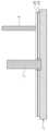
도 3은 본 발명의 실시 예들에 따른 플라즈마 처리 장치의 일부를 나타낸 분해 사시도이다.FIG. 3 is an exploded perspective view showing a part of a plasma processing device according to embodiments of the present invention.
도 3을 참고하면, 정전 척(C)이 플라즈마 전극(7) 상에 제공될 수 있다. 정전 척(C)은 척 바디(Cb), 척 전극(5), 마이크로 히터 층(1), 상부 전극 층(21), 매크로 히터 층(3), 하부 전극 층(23) 및 접지 층(25) 등을 포함할 수 있다.Referring to FIG. 3, an electrostatic chuck (C) may be provided on a plasma electrode (7). The electrostatic chuck (C) may include a chuck body (Cb), a chuck electrode (5), a micro heater layer (1), an upper electrode layer (21), a macro heater layer (3), a lower electrode layer (23), and a ground layer (25).
척 바디(Cb)는 일정 두께를 가지는 원판 형상을 포함할 수 있다. 척 바디(Cb)는 정전 척(C)의 전체적인 외형을 형성할 수 있다. 척 바디(Cb)는 플라즈마 전극(7) 상에 위치할 수 있다. 척 바디(Cb)는 척 전극(5), 마이크로 히터 층(1), 상부 전극 층(21), 매크로 히터 층(3), 하부 전극 층(23) 및 접지 층(25) 등을 고정시킬 수 있다. 즉, 척 전극(5), 마이크로 히터 층(1), 상부 전극 층(21), 매크로 히터 층(3), 하부 전극 층(23) 및 접지 층(25) 등은 척 바디(Cb) 내에 위치할 수 있다. 척 바디(Cb)는 세라믹 등을 포함할 수 있다. 척 바디(Cb)의 상면 상에 웨이퍼(W) 등이 배치될 수 있다.The chuck body (Cb) may include a disc shape having a certain thickness. The chuck body (Cb) may form the overall outer shape of the electrostatic chuck (C). The chuck body (Cb) may be positioned on the plasma electrode (7). The chuck body (Cb) may fix the chuck electrode (5), the micro heater layer (1), the upper electrode layer (21), the macro heater layer (3), the lower electrode layer (23), the ground layer (25), etc. That is, the chuck electrode (5), the micro heater layer (1), the upper electrode layer (21), the macro heater layer (3), the lower electrode layer (23), the ground layer (25), etc. may be positioned within the chuck body (Cb). The chuck body (Cb) may include ceramic, etc. A wafer (W), etc. may be placed on an upper surface of the chuck body (Cb).
척 전극(5)은 척 바디(Cb) 내에 위치할 수 있다. 척 전극(5)은 척 전극 파워 소스(E, 도 1 참고)에 전기적으로 연결될 수 있다. 척 전극(5)은 척 전극 파워 소스(E)로부터 정전압을 전달 받아, 웨이퍼(W)를 고정시킬 수 있다. 예를 들어, 척 전극(5)은 척 전극 파워 소스(E)로부터 약 2500V의 정전압을 제공 받아, 웨이퍼(W)를 정전 척(C) 상에 고정시킬 수 있다. 척 전극(5)은 접지 층(25) 등에 전기적으로 연결될 수 있다.The chuck electrode (5) may be located within the chuck body (Cb). The chuck electrode (5) may be electrically connected to a chuck electrode power source (E, see FIG. 1). The chuck electrode (5) may receive a constant voltage from the chuck electrode power source (E) to fix the wafer (W). For example, the chuck electrode (5) may receive a constant voltage of about 2500 V from the chuck electrode power source (E) to fix the wafer (W) on the electrostatic chuck (C). The chuck electrode (5) may be electrically connected to a ground layer (25), etc.
마이크로 히터 층(1)은 척 바디(Cb) 내에 위치할 수 있다. 마이크로 히터 층(1)은 척 전극(5) 하에 위치할 수 있다. 즉, 척 전극(5)이 마이크로 히터 층(1) 상에 위치할 수 있다. 마이크로 히터 층(1)은 히터 파워 소스(H, 도 1 참고)에 전기적으로 연결될 수 있다. 보다 구체적으로, 마이크로 히터 층(1)은 상부 전극 층(21)을 통해, 히터 파워 소스(H)로부터 히터 파워를 공급받을 수 있다. 마이크로 히터 층(1)은 웨이퍼(W) 등을 가열시킬 수 있다. 마이크로 히터 층(1)은 복수 개의 히터를 포함할 수 있다. 마이크로 히터 층(1)의 복수 개의 히터의 각각은 전도성 물질을 포함할 수 있다. 예를 들어, 마이크로 히터 층(1)의 복수 개의 히터의 각각은 니켈 크롬 합금 등을 포함할 수 있다. 실시 예들에서, 마이크로 히터 층(1)은 웨이퍼(W)의 각 지점의 세부적인 온도를 조절할 수 있다. 마이크로 히터 층(1)의 복수 개의 히터는 평면적 관점에서 원 형상을 형성하도록 배열될 수 있다. 이에 대한 상세한 내용은 도 4 내지 도 7을 참고하여 후술하도록 한다.The micro heater layer (1) may be positioned within the chuck body (Cb). The micro heater layer (1) may be positioned under the chuck electrode (5). That is, the chuck electrode (5) may be positioned on the micro heater layer (1). The micro heater layer (1) may be electrically connected to a heater power source (H, see FIG. 1). More specifically, the micro heater layer (1) may receive heater power from the heater power source (H) through the upper electrode layer (21). The micro heater layer (1) may heat a wafer (W), etc. The micro heater layer (1) may include a plurality of heaters. Each of the plurality of heaters of the micro heater layer (1) may include a conductive material. For example, each of the plurality of heaters of the micro heater layer (1) may include a nickel chromium alloy, etc. In embodiments, the micro heater layer (1) may control a detailed temperature of each point of the wafer (W). A plurality of heaters of the micro heater layer (1) can be arranged to form a circular shape in a planar view. Details on this will be described later with reference to FIGS. 4 to 7.
상부 전극 층(21)은 척 바디(Cb) 내에 위치할 수 있다. 상부 전극 층(21)은 마이크로 히터 층(1) 밑에 위치할 수 있다. 상부 전극 층(21)은 히터 파워 소스(H, 도 1 참고)에 전기적으로 연결될 수 있다. 상부 전극 층(21)은 히터 파워 소스(H)로부터 히터 파워를 공급 받아, 마이크로 히터 층(1)에 히터 파워를 전달할 수 있다. 보다 구체적으로, 상부 전극 층(21)은 히터 파워 소스(H)로부터 공급 받은 히터 파워를 분기시켜 마이크로 히터 층(1)의 복수 개의 히터에 전달할 수 있다. 상부 전극 층(21)은 접지 층(25) 등에 전기적으로 연결될 수 있다.The upper electrode layer (21) may be positioned within the chuck body (Cb). The upper electrode layer (21) may be positioned beneath the micro heater layer (1). The upper electrode layer (21) may be electrically connected to a heater power source (H, see FIG. 1). The upper electrode layer (21) may receive heater power from the heater power source (H) and transmit the heater power to the micro heater layer (1). More specifically, the upper electrode layer (21) may branch the heater power supplied from the heater power source (H) and transmit the branched heater power to a plurality of heaters of the micro heater layer (1). The upper electrode layer (21) may be electrically connected to a ground layer (25), etc.
매크로 히터 층(3)은 척 바디(Cb) 내에 위치할 수 있다. 매크로 히터 층(3)은 상부 전극 층(21) 하에 위치할 수 있다. 즉, 상부 전극 층(21)이 매크로 히터 층(3) 상에 위치할 수 있다. 매크로 히터 층(3)은 히터 파워 소스(H, 도 1 참고)에 전기적으로 연결될 수 있다. 보다 구체적으로, 매크로 히터 층(3)은 하부 전극 층(23)을 통해, 히터 파워 소스(H)로부터 히터 파워를 공급받을 수 있다. 매크로 히터 층(3)은 웨이퍼(W) 등을 가열시킬 수 있다. 매크로 히터 층(3)은 복수 개의 히터를 포함할 수 있다. 매크로 히터 층(3)의 복수 개의 히터의 각각은 전도성 물질을 포함할 수 있다. 예를 들어, 매크로 히터 층(3)의 복수 개의 히터의 각각은 니켈 크롬 합금 등을 포함할 수 있다. 복수 개의 히터의 각각은 원주 방향으로 연장될 수 있다. 복수 개의 히터의 각각은 서로 지름 방향으로 이격될 수 있다. 실시 예들에서, 매크로 히터 층(3)은 웨이퍼(W)의 개략적인 온도를 조절할 수 있다.The macro heater layer (3) may be positioned within the chuck body (Cb). The macro heater layer (3) may be positioned under the upper electrode layer (21). That is, the upper electrode layer (21) may be positioned on the macro heater layer (3). The macro heater layer (3) may be electrically connected to a heater power source (H, see FIG. 1). More specifically, the macro heater layer (3) may receive heater power from the heater power source (H) through the lower electrode layer (23). The macro heater layer (3) may heat a wafer (W), etc. The macro heater layer (3) may include a plurality of heaters. Each of the plurality of heaters of the macro heater layer (3) may include a conductive material. For example, each of the plurality of heaters of the macro heater layer (3) may include a nickel chromium alloy, etc. Each of the plurality of heaters may extend in the circumferential direction. Each of the plurality of heaters may be spaced apart from each other in the radial direction. In embodiments, the macro heater layer (3) can control the approximate temperature of the wafer (W).
하부 전극 층(23)은 척 바디(Cb) 내에 위치할 수 있다. 하부 전극 층(23)은 매크로 히터 층(3) 밑에 위치할 수 있다. 하부 전극 층(23)은 히터 파워 소스(H, 도 1 참고)에 전기적으로 연결될 수 있다. 하부 전극 층(23)은 히터 파워 소스(H)로부터 히터 파워를 공급 받아, 매크로 히터 층(3)에 히터 파워를 전달할 수 있다. 보다 구체적으로, 하부 전극 층(23)은 히터 파워 소스(H)로부터 공급 받은 히터 파워를 분기시켜 매크로 히터 층(3)의 복수 개의 히터에 전달할 수 있다. 하부 전극 층(23)은 접지 층(25) 등에 전기적으로 연결될 수 있다.The lower electrode layer (23) may be positioned within the chuck body (Cb). The lower electrode layer (23) may be positioned beneath the macro heater layer (3). The lower electrode layer (23) may be electrically connected to a heater power source (H, see FIG. 1). The lower electrode layer (23) may receive heater power from the heater power source (H) and transmit the heater power to the macro heater layer (3). More specifically, the lower electrode layer (23) may branch the heater power supplied from the heater power source (H) and transmit the branched heater power to a plurality of heaters of the macro heater layer (3). The lower electrode layer (23) may be electrically connected to a ground layer (25), etc.
접지 층(25)은 척 바디(Cb) 내에 위치할 수 있다. 접지 층(25)은 하부 전극 층(23) 밑에 위치할 수 있다. 접지 층(25)은 전도성 물질을 포함할 수 있다. 예를 들어, 접지 층(25)은 금속 디스크 등을 포함할 수 있다. 접지 층(25)은 척 전극(5), 상부 전극 층(21) 및 하부 전극 층(23) 등을 접지시킬 수 있다.The ground layer (25) may be located within the chuck body (Cb). The ground layer (25) may be located beneath the lower electrode layer (23). The ground layer (25) may include a conductive material. For example, the ground layer (25) may include a metal disk, etc. The ground layer (25) may ground the chuck electrode (5), the upper electrode layer (21), the lower electrode layer (23), etc.
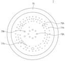
도 4는 본 발명의 실시 예들에 따른 정전 척의 마이크로 히터 층을 나타낸 평면도이고, 도 5는 본 발명의 실시 예들에 따른 정전 척의 마이크로 히터 층에서 영역 구분을 설명하기 위해 히터만을 제거하고 나타낸 평면도이다.FIG. 4 is a plan view showing a micro heater layer of an electrostatic chuck according to embodiments of the present invention, and FIG. 5 is a plan view showing only the heater removed to explain the division of regions in the micro heater layer of an electrostatic chuck according to embodiments of the present invention.
도 4를 참고하면, 마이크로 히터 층(1)은 내측 영역(11) 및 외측 영역(13)으로 구분될 수 있다.Referring to Fig. 4, the micro heater layer (1) can be divided into an inner region (11) and an outer region (13).
내측 영역(11)은 마이크로 히터 층(1)에서 안쪽에 가까운 영역을 의미할 수 있다. 즉, 내측 영역(11)은 마이크로 히터 층(1)의 중심(M)에 가까운 영역 및/또는 마이크로 히터 층(1)의 중심(M)을 포함하는 영역을 의미할 수 있다. 마이크로 히터 층(1)의 중심(M)은, 원 형태를 형성하는 마이크로 히터 층(1)에서, 원의 중심 또는 원의 중심에 가까운 지점을 의미할 수 있다. 내측 영역(11)은 제1 내측 영역(111), 제2 내측 영역(113), 제3 내측 영역(115) 및 제4 내측 영역(117) 등으로 구분될 수 있다. 제1 내측 영역(111)은 마이크로 히터 층(1)의 중심(M)을 평면적 관점에서 원주 방향으로 둘러 쌀 수 있다. 예를 들어, 제1 내측 영역(111)은 중심(M)으로부터 제1 내측 거리 내지 제2 내측 거리만큼 떨어진 영역을 의미할 수 있다. 제2 내측 영역(113)은 제1 내측 영역(111)의 외측에서 제1 내측 영역(111)을 평면적 관점에서 원주 방향으로 둘러 쌀 수 있다. 예를 들어, 제2 내측 영역(113)은 중심(M)으로부터 제2 내측 거리 내지 제3 내측 거리만큼 떨어진 영역을 의미할 수 있다. 제3 내측 영역(115)은 제2 내측 영역(113)의 외측에서 제2 내측 영역(113)을 원주 방향으로 둘러 쌀 수 있다. 예를 들어, 제3 내측 영역(115)은 중심(M)으로부터 제3 내측 거리 내지 제4 내측 거리만큼 떨어진 영역을 의미할 수 있다. 제4 내측 영역(117)은 제3 내측 영역(115)의 외측에서 제3 내측 영역(115)을 원주 방향으로 둘러 쌀 수 있다. 예를 들어, 제4 내측 영역(117)은 중심(M)으로부터 제4 내측 거리 내지 제5 내측 거리만큼 떨어진 영역을 의미할 수 있다. 이상에서, 내측 영역(11)이 제1 내측 영역(111), 제2 내측 영역(113), 제3 내측 영역(115) 및 제4 내측 영역(117)의 4개의 영역으로 구분되는 것으로 서술하였으나, 이는 발명의 설명을 돕기 위한 실시 예일 뿐, 내측 영역(11)은 1개, 2개, 3개 또는 5개 이상의 영역으로 구분될 수도 있다. 내측 영역(11)이 1개의 영역으로 구분된다는 것은, 내측 영역(11)과 제1 내측 영역(111)이 실질적으로 동일하다는 것을 의미할 수 있다. 도 5를 참고하면, 제1 내측 영역(111)은 원주 방향을 따라 복수 개의 제1 미세 내측 영역(1111)으로 구분될 수 있다. 제1 미세 내측 영역(1111)은 원주 방향을 따라 구획된 섹터를 의미할 수 있다. 예를 들어, 제1 내측 영역(111)은 8개의 제1 미세 내측 영역(1111)으로 나뉠 수 있다. 마찬가지로 제2 내측 영역(113)은 원주 방향을 따라 복수 개의 제2 미세 내측 영역(1131)으로 구분될 수 있다. 예를 들어, 제2 내측 영역(113)은 16개의 제2 미세 내측 영역(1131)으로 나뉠 수 있다. 제3 내측 영역(115)은 원주 방향을 따라 복수 개의 제3 미세 내측 영역(1151)으로 구분될 수 있다. 예를 들어, 제3 내측 영역(115)은 26개의 제3 미세 내측 영역(1151)으로 나뉠 수 있다. 제4 내측 영역(117)은 원주 방향을 따라 복수 개의 제4 미세 내측 영역(1171)으로 구분될 수 있다. 예를 들어, 제4 내측 영역(117)은 26개의 제4 미세 내측 영역(1171)로 나뉠 수 있다.The inner region (11) may mean a region close to the inside in the micro heater layer (1). That is, the inner region (11) may mean a region close to the center (M) of the micro heater layer (1) and/or a region including the center (M) of the micro heater layer (1). The center (M) of the micro heater layer (1) may mean the center of the circle or a point close to the center of the circle in the micro heater layer (1) forming a circular shape. The inner region (11) may be divided into a first inner region (111), a second inner region (113), a third inner region (115), and a fourth inner region (117). The first inner region (111) may surround the center (M) of the micro heater layer (1) in a circumferential direction in a planar view. For example, the first inner region (111) may mean a region that is spaced apart from the center (M) by a first inner distance or a second inner distance. The second inner region (113) can circumferentially surround the first inner region (111) from the outside of the first inner region (111) in a planar view. For example, the second inner region (113) can mean a region that is spaced apart from the center (M) by a second inner distance to a third inner distance. The third inner region (115) can circumferentially surround the second inner region (113) from the outside of the second inner region (113). For example, the third inner region (115) can mean a region that is spaced apart from the center (M) by a third inner distance to a fourth inner distance. The fourth inner region (117) can circumferentially surround the third inner region (115) from the outside of the third inner region (115). For example, the fourth inner region (117) may mean a region that is spaced apart from the center (M) by a fourth inner distance to a fifth inner distance. In the above, the inner region (11) is described as being divided into four regions of the first inner region (111), the second inner region (113), the third inner region (115), and the fourth inner region (117), but this is only an example to help explain the invention, and the inner region (11) may be divided into one, two, three, or five or more regions. The fact that the inner region (11) is divided into one region may mean that the inner region (11) and the first inner region (111) are substantially the same. Referring to FIG. 5, the first inner region (111) may be divided into a plurality of first micro inner regions (1111) along the circumferential direction. The first micro inner region (1111) may mean a sector divided along a circumferential direction. For example, the first inner region (111) may be divided into eight first micro inner regions (1111). Similarly, the second inner region (113) may be divided into a plurality of second micro inner regions (1131) along a circumferential direction. For example, the second inner region (113) may be divided into sixteen second micro inner regions (1131). The third inner region (115) may be divided into a plurality of third micro inner regions (1151) along a circumferential direction. For example, the third inner region (115) may be divided into twenty-six third micro inner regions (1151). The fourth inner region (117) may be divided into a plurality of fourth micro inner regions (1171) along a circumferential direction. For example, the fourth inner region (117) can be divided into 26 fourth micro inner regions (1171).
다시 도 4를 참고하면, 외측 영역(13)은 내측 영역(11)을 평면적 관점에서 둘러 싸는 영역을 의미할 수 있다. 즉, 외측 영역(13)은 내측 영역(11)을 기준으로, 마이크로 히터 층(1)의 중심(M)에서 먼 쪽을 의미할 수 있다. 외측 영역(13)은 제1 외측 영역(131), 제2 외측 영역(133) 및 제3 외측 영역(135) 등으로 구분될 수 있다. 제1 외측 영역(131)은 평면적 관점에서 제4 내측 영역(117)을 원주 방향으로 둘러 쌀 수 있다. 예를 들어, 제1 외측 영역(131)은 중심(M)으로부터 제1 외측 거리 내지 제2 외측 거리만큼 떨어진 영역을 의미할 수 있다. 실시 예들에서, 내측 영역(11)이 4개로 분할되는 경우, 제5 내측 거리와 제1 외측 거리는 실질적으로 동일 또는 유사할 수 있다. 제2 외측 영역(133)은 제1 외측 영역(131)의 외측에서 제1 외측 영역(131)을 평면적 관점에서 원주 방향으로 둘러 쌀 수 있다. 예를 들어, 제2 외측 영역(133)은 중심(M)으로부터 제2 외측 거리 내지 제3 외측 거리만큼 떨어진 영역을 의미할 수 있다. 제3 외측 영역(135)은 제2 외측 영역(133)의 외측에서 제2 외측 영역(133)을 원주 방향으로 둘러 쌀 수 있다. 이상에서, 외측 영역(13)이 제1 외측 영역(131), 제2 외측 영역(133) 및 제3 외측 영역(135)의 3개의 영역으로 구분되는 것으로 서술하였으나, 이는 발명의 설명을 돕기 위한 실시 예일 뿐, 외측 영역(13)은 2개 또는 4개 이상의 영역으로 구분될 수도 있다. 다시 도 5를 참고하면, 제1 외측 영역(131)은 원주 방향을 따라 복수 개의 제1 미세 외측 영역(1311)으로 구분될 수 있다. 제1 미세 외측 영역(1311)은 원주 방향을 따라 구획된 섹터를 의미할 수 있다. 예를 들어, 제1 외측 영역(131)은 28개의 제1 미세 외측 영역(1311)으로 나뉠 수 있다. 마찬가지로 제2 외측 영역(133)은 원주 방향을 따라 복수 개의 제2 미세 외측 영역(1331)으로 구분될 수 있다. 예를 들어, 제2 외측 영역(133)은 32개의 제2 미세 외측 영역(1331)으로 나뉠 수 있다. 제3 외측 영역(135)은 원주 방향을 따라 복수 개의 제3 미세 외측 영역(1351)으로 구분될 수 있다. 예를 들어, 제3 외측 영역(135)은 32개의 제3 미세 외측 영역(1351)으로 나뉠 수 있다.Referring again to FIG. 4, the outer region (13) may mean a region surrounding the inner region (11) in a planar view. That is, the outer region (13) may mean a region farther away from the center (M) of the micro heater layer (1) with respect to the inner region (11). The outer region (13) may be divided into a first outer region (131), a second outer region (133), a third outer region (135), etc. The first outer region (131) may surround the fourth inner region (117) in a circumferential direction in a planar view. For example, the first outer region (131) may mean a region that is spaced apart from the center (M) by a first outer distance or a second outer distance. In embodiments, when the inner region (11) is divided into four, the fifth inner distance and the first outer distance may be substantially the same or similar. The second outer region (133) can surround the first outer region (131) in a circumferential direction from a planar viewpoint on the outside of the first outer region (131). For example, the second outer region (133) can mean a region that is spaced apart from the center (M) by a second outer distance to a third outer distance. The third outer region (135) can surround the second outer region (133) in a circumferential direction on the outside of the second outer region (133). In the above, the outer region (13) is described as being divided into three regions of the first outer region (131), the second outer region (133), and the third outer region (135), but this is only an example to help explain the invention, and the outer region (13) may be divided into two or four or more regions. Referring again to FIG. 5, the first outer region (131) can be divided into a plurality of first micro outer regions (1311) along the circumferential direction. The first micro outer region (1311) can mean a sector partitioned along the circumferential direction. For example, the first outer region (131) can be divided into 28 first micro outer regions (1311). Similarly, the second outer region (133) can be divided into a plurality of second micro outer regions (1331) along the circumferential direction. For example, the second outer region (133) can be divided into 32 second micro outer regions (1331). The third outer region (135) can be divided into a plurality of third micro outer regions (1351) along the circumferential direction. For example, the third outer region (135) can be divided into 32 third micro outer regions (1351).
다시 도 4를 참고하면, 마이크로 히터 층(1)은 내측 히터부(11h) 및 외측 히터부(13h)를 포함할 수 있다. 내측 히터부(11h) 및 외측 히터부(13h)는 히터 파워 소스(H, 도 1 참고)에 연결될 수 있다. 보다 구체적으로, 내측 히터부(11h) 및 외측 히터부(13h)는 상부 전극 층(21, 도 3 참고)을 통해 히터 파워 소스(H)에 연결될 수 있다. 내측 히터부(11h) 및 외측 히터부(13h)는 히터 파워 소스(H)로부터 히터 파워를 공급 받을 수 있다.Referring again to FIG. 4, the micro heater layer (1) may include an inner heater part (11h) and an outer heater part (13h). The inner heater part (11h) and the outer heater part (13h) may be connected to a heater power source (H, see FIG. 1). More specifically, the inner heater part (11h) and the outer heater part (13h) may be connected to the heater power source (H) through the upper electrode layer (21, see FIG. 3). The inner heater part (11h) and the outer heater part (13h) may receive heater power from the heater power source (H).
내측 히터부(11h)는 내측 영역(11)에 위치할 수 있다. 즉, 내측 히터부(11h)는 마이크로 히터 층(1)의 내측에 위치할 수 있다. 내측 히터부(11h)는 제1 내측 히터(111h), 제2 내측 히터(113h), 제3 내측 히터(115h) 및 제4 내측 히터(117h)를 포함할 수 있다. 제1 내측 히터(111h)는 제1 내측 영역(111) 내에(in) 위치할 수 있다. 제1 내측 영역(111)이 복수 개의 제1 미세 내측 영역(1111, 도 5 참고)으로 구분되는 경우, 제1 내측 히터(111h)는 복수 개의 제1 미세 내측 영역(1111)의 각각의 안에(in) 제공될 수 있다. 실시 예들에서, 제1 내측 영역(111)이 복수 개의 제1 미세 내측 영역(1111)으로 구분되지 아니하고 단일 영역을 구성하는 경우, 제1 내측 히터(111h)는 마이크로 히터 층(1)의 중심(M)을 원주 방향으로 전부 또는 대부분 둘러 싸는 띠(band) 형태의 히터일 수 있다. 제2 내측 히터(113h)는 제2 내측 영역(113) 내에 위치할 수 있다. 제2 내측 영역(113)이 복수 개의 제2 미세 내측 영역(1131, 도 5 참고)으로 구분되는 경우, 제2 내측 히터(113h)는 복수 개의 제2 미세 내측 영역(1131)의 각각의 안에 제공될 수 있다. 제3 내측 히터(115h) 및 제4 내측 히터(117h)도 마찬가지로 제3 내측 영역(115) 및 제4 내측 영역(117) 내에 위치할 수 있다.The inner heater part (11h) may be located in the inner region (11). That is, the inner heater part (11h) may be located on the inner side of the micro heater layer (1). The inner heater part (11h) may include a first inner heater (111h), a second inner heater (113h), a third inner heater (115h), and a fourth inner heater (117h). The first inner heater (111h) may be located in the first inner region (111). When the first inner region (111) is divided into a plurality of first micro inner regions (1111, see FIG. 5), the first inner heater (111h) may be provided in each of the plurality of first micro inner regions (1111). In embodiments, when the first inner region (111) is not divided into a plurality of first micro inner regions (1111) but constitutes a single region, the first inner heater (111h) may be a band-shaped heater that circumferentially surrounds the center (M) of the micro heater layer (1) entirely or mostly. The second inner heater (113h) may be located within the second inner region (113). When the second inner region (113) is divided into a plurality of second micro inner regions (1131, see FIG. 5), the second inner heater (113h) may be provided within each of the plurality of second micro inner regions (1131). The third inner heater (115h) and the fourth inner heater (117h) may likewise be located within the third inner region (115) and the fourth inner region (117).
외측 히터부(13h)는 외측 영역(13)에 위치할 수 있다. 따라서 외측 히터부(13h)는 내측 히터부(11h)의 외측에 위치할 수 있다. 외측 히터부(13h)는 제1 외측 히터(131h), 제2 외측 히터(133h) 및 제3 외측 히터(135h)를 포함할 수 있다. 제1 외측 히터(131h)는 제1 외측 영역(131) 내에 위치할 수 있다. 제1 외측 영역(131)이 복수 개의 제1 미세 외측 영역(1311, 도 5 참고)으로 구분되는 경우, 제1 외측 히터(131h)는 복수 개의 제1 미세 외측 영역(1311)의 각각의 안에(in) 제공될 수 있다. 제2 외측 히터(133h)는 제2 외측 영역(133) 내에 위치할 수 있다. 제2 외측 영역(133)이 복수 개의 제2 미세 외측 영역(1331, 도 5 참고)으로 구분되는 경우, 제2 외측 히터(133h)는 복수 개의 제2 미세 외측 영역(1331)의 각각의 안에 제공될 수 있다. 제3 외측 히터(135h)도 마찬가지로 제3 외측 영역(135) 내에 위치할 수 있다.The outer heater part (13h) may be located in the outer region (13). Therefore, the outer heater part (13h) may be located outside the inner heater part (11h). The outer heater part (13h) may include a first outer heater (131h), a second outer heater (133h), and a third outer heater (135h). The first outer heater (131h) may be located in the first outer region (131). When the first outer region (131) is divided into a plurality of first micro outer regions (1311, see FIG. 5), the first outer heater (131h) may be provided in each of the plurality of first micro outer regions (1311). The second outer heater (133h) may be located in the second outer region (133). When the second outer region (133) is divided into a plurality of second micro outer regions (1331, see FIG. 5), the second outer heater (133h) may be provided within each of the plurality of second micro outer regions (1331). The third outer heater (135h) may likewise be located within the third outer region (135).
다시 도 5를 참고하면, 마이크로 히터 층(1)의 중심(M)으로부터 제1 외측 영역(131)까지의 지름 방향으로의 거리가 외측 경계 거리(N)로 정의될 수 있다. 예를 들어, 외측 경계 거리(N)는 제1 외측 거리일 수 있다. 실시 예들에서, 외측 경계 거리(N)는 120mm 이상, 130mm 이하일 수 있다. 보다 구체적으로, 외측 경계 거리(N)는 약 125mm일 수 있다. 그러나 이에 한정하는 것은 아니다.Referring again to FIG. 5, a distance in the radial direction from the center (M) of the micro heater layer (1) to the first outer region (131) may be defined as an outer boundary distance (N). For example, the outer boundary distance (N) may be the first outer distance. In embodiments, the outer boundary distance (N) may be 120 mm or more and 130 mm or less. More specifically, the outer boundary distance (N) may be about 125 mm. However, the present invention is not limited thereto.
도 6은 도 4의 일부를 확대한 평면도이다.Figure 6 is an enlarged plan view of a portion of Figure 4.
도 6을 참고하면, 제3 내측 영역(115)의 지름 방향으로의 두께는 제3 내측 두께(ri)로 명명될 수 있다. 예를 들어, 제3 내측 두께(ri)는 제4 내측 거리와 제3 내측 거리의 차이에 해당할 수 있다. 제4 내측 영역(117)의 지름 방향으로의 두께는 제4 내측 두께(ri')로 명명될 수 있다. 예를 들어, 제4 내측 두께(ri)는 제5 내측 거리와 제4 내측 거리의 차이에 해당할 수 있다. 도 6에 도시되지는 아니하였지만, 제1 내측 영역(111, 도 5 등 참고)의 지름 방향으로의 두께는 제1 내측 두께로 명명될 수 있다. 예를 들어, 제1 내측 두께는 제2 내측 거리와 제1 내측 거리의 차이에 해당할 수 있다. 제2 내측 영역(113)의 지름 방향으로의 두께는 제2 내측 두께로 명명될 수 있다. 예를 들어, 제2 내측 두께는 제3 내측 거리와 제2 내측 거리의 차이에 해당할 수 있다. 제3 내측 히터(115h)의 중심과 제4 내측 히터(117h)의 중심 사이의 지름 방향으로의 거리는 제3 내측 이격 거리(si)로 명명될 수 있다. 제4 내측 히터(117h)의 중심과 제1 외측 히터(131h)의 중심 사이의 지름 방향으로의 거리는 제4 내측 이격 거리(si')로 명명될 수 있다. 도 6에는 도시되지는 아니하였지만, 제1 내측 히터(111h)의 중심과 제2 내측 히터(113h)의 중심 사이의 지름 방향으로의 거리는 제1 내측 이격 거리로 명명될 수 있고, 제2 내측 히터(113h)의 중심과 제3 내측 히터(115h)의 중심 사이의 지름 방향으로의 거리는 제2 내측 이격 거리로 명명될 수 있다. 실시 예들에서, 히터의 중심이라는 용어는, 평면적 관점에서 히터가 차지하는 면적의 무게 중심을 의미할 수 있다. 예를 들어, 하나의 히터의 둘레가 평면적 관점에서 직사각형을 포함하는 경우, 히터의 중심은 직사각형의 무게 중심을 의미할 수 있다. 실시 예들에서, 제1 내측 영역(111)이 복수 개의 제1 미세 영역(1111)으로 구분되지 아니하는 경우, 제1 내측 히터(111h)의 중심은 마이크로 히터 층(1)의 중심(M)을 둘러 싸는 원의 전부 또는 일부일 수 있다. 이 경우 제1 내측 히터(111h)의 중심과 제2 내측 히터(113h)의 중심 사이의 지름 방향으로의 거리는, 두 원 사이의 지름 방향으로의 거리를 의미할 수 있다.Referring to FIG. 6, the thickness in the radial direction of the third inner region (115) may be named as the third inner thickness (ri). For example, the third inner thickness (ri) may correspond to the difference between the fourth inner distance and the third inner distance. The thickness in the radial direction of the fourth inner region (117) may be named as the fourth inner thickness (ri'). For example, the fourth inner thickness (ri) may correspond to the difference between the fifth inner distance and the fourth inner distance. Although not shown in FIG. 6, the thickness in the radial direction of the first inner region (111, see FIG. 5, etc.) may be named as the first inner thickness. For example, the first inner thickness may correspond to the difference between the second inner distance and the first inner distance. The thickness in the radial direction of the second inner region (113) may be named as the second inner thickness. For example, the second inner thickness may correspond to a difference between the third inner distance and the second inner distance. A radial distance between the center of the third inner heater (115h) and the center of the fourth inner heater (117h) may be referred to as a third inner separation distance (si). A radial distance between the center of the fourth inner heater (117h) and the center of the first outer heater (131h) may be referred to as a fourth inner separation distance (si'). Although not shown in FIG. 6, a radial distance between the center of the first inner heater (111h) and the center of the second inner heater (113h) may be referred to as a first inner separation distance, and a radial distance between the center of the second inner heater (113h) and the center of the third inner heater (115h) may be referred to as a second inner separation distance. In the embodiments, the term center of the heater may mean the center of gravity of the area occupied by the heater in a planar view. For example, if the perimeter of one heater includes a rectangle in a planar view, the center of the heater may mean the center of gravity of the rectangle. In the embodiments, if the first inner region (111) is not divided into a plurality of first micro regions (1111), the center of the first inner heater (111h) may be all or part of a circle surrounding the center (M) of the micro heater layer (1). In this case, the radial distance between the center of the first inner heater (111h) and the center of the second inner heater (113h) may mean the radial distance between the two circles.
제1 외측 영역(131)의 지름 방향으로의 두께는 제1 외측 두께(re)로 명명될 수 있다. 예를 들어, 제1 외측 두께(re)는 제2 외측 거리와 제1 외측 거리의 차이에 해당할 수 있다. 제2 외측 영역(133)의 지름 방향으로의 두께는 제2 외측 두께(re')로 명명될 수 있다. 예를 들어, 제2 외측 두께(re')는 제3 외측 거리와 제2 외측 거리의 차이에 해당할 수 있다. 제3 외측 영역(135)의 지름 방향으로의 두께는 제3 외측 두께(re'')로 명명될 수 있다. 제1 외측 히터(131h)의 중심과 제2 외측 히터(133h)의 중심 사이의 지름 방향으로의 거리는 제1 외측 이격 거리(se)로 명명될 수 있다. 제2 외측 히터(133h)의 중심과 제3 외측 히터(135h)의 중심 사이의 지름 방향으로의 거리는 제2 외측 이격 거리(se')로 명명될 수 있다.The thickness in the diametric direction of the first outer region (131) may be referred to as the first outer thickness (re). For example, the first outer thickness (re) may correspond to the difference between the second outer distance and the first outer distance. The thickness in the diametric direction of the second outer region (133) may be referred to as the second outer thickness (re'). For example, the second outer thickness (re') may correspond to the difference between the third outer distance and the second outer distance. The thickness in the diametric direction of the third outer region (135) may be referred to as the third outer thickness (re''). The diametric distance between the center of the first outer heater (131h) and the center of the second outer heater (133h) may be referred to as the first outer separation distance (se). The radial distance between the center of the second outer heater (133h) and the center of the third outer heater (135h) may be referred to as the second outer separation distance (se').
실시 예들에서, 제1 외측 두께(re), 제2 외측 두께(re') 및 제3 외측 두께(re'') 중 적어나 하나 이상은, 제1 내측 두께, 제2 내측 두께, 제3 내측 두께(ri) 및 제4 내측 두께(ri') 중 가장 작은 것보다 작을 수 있다. 즉, 제1 외측 영역(131), 제2 외측 영역(133) 및 제3 외측 영역(135) 중 적어도 하나 이상은, 제1 내측 영역(111), 제2 내측 영역(113), 제3 내측 영역(115) 및 제4 내측 영역(117) 중 가장 얇은 것보다 얇을 수 있다. 예를 들어, 제1 외측 두께(re), 제2 외측 두께(re') 및 제3 외측 두께(re'')의 각각은 모두 제1 내측 두께, 제2 내측 두께, 제3 내측 두께(ri) 및 제4 내측 두께(ri') 중 가장 작은 것보다 작을 수 있다. 혹은, 내측 영역(11)이 1개의 영역만으로 구분되어 내측 영역(11)이 제1 내측 영역(111)과 실질적으로 동일 또는 유사한 경우, 제1 외측 두께(re), 제2 외측 두께(re') 및 제3 외측 두께(re'') 중 적어도 하나 이상이 제1 내측 두께보다 작을 수 있다.In embodiments, at least one of the first outer thickness (re), the second outer thickness (re'), and the third outer thickness (re'') may be smaller than a smallest one of the first inner thickness, the second inner thickness, the third inner thickness (ri), and the fourth inner thickness (ri'). That is, at least one of the first outer region (131), the second outer region (133), and the third outer region (135) may be thinner than a smallest one of the first inner region (111), the second inner region (113), the third inner region (115), and the fourth inner region (117). For example, each of the first outer thickness (re), the second outer thickness (re'), and the third outer thickness (re'') may be smaller than a smallest one of the first inner thickness, the second inner thickness, the third inner thickness (ri), and the fourth inner thickness (ri'). Alternatively, if the inner region (11) is divided into only one region and the inner region (11) is substantially identical or similar to the first inner region (111), at least one of the first outer thickness (re), the second outer thickness (re'), and the third outer thickness (re'') may be smaller than the first inner thickness.
제1 외측 이격 거리(se) 및 제2 외측 이격 거리(se') 중 적어도 하나는, 제1 내측 이격 거리, 제2 내측 이격 거리, 제3 내측 이격 거리(si) 및 제4 내측 이격 거리(si') 중 작은 것보다 작을 수 있다. 예를 들어, 제1 외측 이격 거리(se)는 제1 내측 이격 거리 및 제2 내측 이격 거리보다 작을 수 있다. 제1 외측 히터(131h)와 제2 외측 히터(133h) 사이의 지름방향으로의 간격은, 제1 내측 히터(111h)와 제2 내측 히터(113h) 사이의 지름 방향으로의 간격보다 작을 수 있다. 즉, 외측 히터는 내측 히터보다 지름 방향으로 촘촘하게 배치될 수 있다. 제4 내측 이격 거리(si')는 제1 내측 이격 거리, 제2 내측 이격 거리 및 제3 내측 이격 거리(si)보다 작을 수 있다.At least one of the first outer spacing distance (se) and the second outer spacing distance (se') may be smaller than a smaller one of the first inner spacing distance, the second inner spacing distance, the third inner spacing distance (si), and the fourth inner spacing distance (si'). For example, the first outer spacing distance (se) may be smaller than the first inner spacing distance and the second inner spacing distance. The radial spacing between the first outer heater (131h) and the second outer heater (133h) may be smaller than the radial spacing between the first inner heater (111h) and the second inner heater (113h). That is, the outer heaters may be arranged diametrically closer together than the inner heaters. The fourth inner spacing distance (si') may be smaller than the first inner spacing distance, the second inner spacing distance, and the third inner spacing distance (si).
다시 도 5 및 도 6을 참고하면, 제1 미세 외측 영역(1311), 제2 미세 외측 영역(1331) 및/또는 제3 미세 외측 영역(1351)의 원주 방향으로의 폭(d1)은 15mm 내지 20mm일 수 있다. 그러나 이에 한정하는 것은 아니며, 구체적 설계 적용에 따라 다른 수치가 선정될 수도 있다.Referring again to FIGS. 5 and 6, the circumferential width (d1) of the first micro outer region (1311), the second micro outer region (1331), and/or the third micro outer region (1351) may be 15 mm to 20 mm. However, this is not limited thereto, and other values may be selected depending on specific design applications.
본 발명의 정전 척 및 이를 포함하는 플라즈마 처리 장치를 이용한 반도체 소자 제조방법에 의하면, 웨이퍼의 온도제어가 가능할 수 있다. 다시 도 1을 참고하면, 웨이퍼(W)를 플라즈마 챔버(R) 내에 삽입하여, 정전 척(C) 상에 배치할 수 있다. 정전 척(C) 상에 배치된 웨이퍼(W)의 온도를 측정하여 웨이퍼(W)의 온도를 제어할 수 있다. 웨이퍼(W)는 반경 방향에 따라 다른 온도로 가열할 필요가 있을 수 있다. 다시 도 4를 참고하면, 제1 외측 영역(131)과 제2 외측 영역(133)의 온도를 다르게 제어할 수 있다. 예를 들어, 제어부(T)는 히터 파워 소스(H)를 제어하여, 제1 외측 영역(131)에 위치한 제1 외측 히터(131h)를 제1 온도로 가열할 수 있다. 동시에, 제어부(T)는 히터 파워 소스(H)를 제어하여, 제2 외측 영역(133)에 위치한 제2 외측 히터(133h)를 제2 온도로 가열할 수 있다. 제1 온도와 제2 온도는 구별될 수 있다. 즉, 제1 온도와 제2 온도는 다를 수 있다. 따라서 웨이퍼(W)의 에지 영역을 지름 방향으로 미세하게 구분하여 가열할 수 있다.According to the method for manufacturing a semiconductor device using the electrostatic chuck of the present invention and the plasma processing device including the same, temperature control of a wafer may be possible. Referring again to FIG. 1, a wafer (W) may be inserted into a plasma chamber (R) and placed on an electrostatic chuck (C). The temperature of the wafer (W) placed on the electrostatic chuck (C) may be measured to control the temperature of the wafer (W). The wafer (W) may need to be heated to different temperatures depending on the radial direction. Referring again to FIG. 4, the temperatures of the first outer region (131) and the second outer region (133) may be controlled differently. For example, the control unit (T) may control the heater power source (H) to heat the first outer heater (131h) located in the first outer region (131) to the first temperature. At the same time, the control unit (T) can control the heater power source (H) to heat the second outer heater (133h) located in the second outer region (133) to the second temperature. The first temperature and the second temperature can be distinguished. That is, the first temperature and the second temperature can be different. Accordingly, the edge region of the wafer (W) can be heated by finely dividing it in the diameter direction.
실시 예들에서, 제어부(T)는 웨이퍼(W)의 온도를 측정하여 발생한 정보를 수신할 수 있다. 제어부(T)는 측정된 웨이퍼(W)의 구간 별 온도에 대한 정보를 이용하여, 웨이퍼(W)에 필요한 가열 정도를 계산할 수 있다. 제어부(T)는 웨이퍼(W)에 필요한 가열 정도를 계산하여 히터 파워 소스(H)를 제어함으로써, 웨이퍼(W)에 대한 미세한 온도 조절이 가능할 수 있다.In embodiments, the control unit (T) can receive information generated by measuring the temperature of the wafer (W). The control unit (T) can calculate the degree of heating required for the wafer (W) using the information on the measured temperature of each section of the wafer (W). The control unit (T) calculates the degree of heating required for the wafer (W) and controls the heater power source (H), thereby enabling fine temperature control for the wafer (W).
본 발명의 예시적인 실시 예들에 따른 정전 척 및 이를 포함하는 플라즈마 처리 장치에 의하면, 외측 영역이 지름 방향으로 복수 개로 나뉘고, 복수 개의 외측 영역의 각각에 외측 히터가 위치할 수 있다. 또한, 복수 개의 외측 영역의 각각의 지름 방향으로의 두께는, 내측 영역의 지름 방향으로의 두께보다 작을 수 있다. 즉, 외측 영역에 히터가 지름 방향으로 더 조밀하게 배치될 수 있다. 이에 따라 외측 영역에서 지름 방향으로 미세한 온도 제어가 가능할 수 있다. 예를 들어, 웨이퍼의 에지 영역에서 지름 방향으로 미세한 온도 제어가 요구되는 경우, 지름 방향으로 세밀하게 배치될 복수 개의 외측 히터를 이용하여 요구되는 온도 제어를 수행할 수 있다. 따라서 웨이퍼의 에지 영역에서의 산포를 개선할 수 있고, 이에 따라 반도체 공정의 수율이 향상될 수 있다.According to an electrostatic chuck and a plasma processing device including the same according to exemplary embodiments of the present invention, an outer region may be divided into a plurality of regions in the radial direction, and an outer heater may be positioned in each of the plurality of outer regions. In addition, a thickness of each of the plurality of outer regions in the radial direction may be smaller than a thickness of the inner region in the radial direction. That is, heaters may be arranged more densely in the outer region in the radial direction. Accordingly, fine temperature control in the radial direction may be possible in the outer region. For example, when fine temperature control in the radial direction is required in an edge region of a wafer, the required temperature control can be performed using a plurality of outer heaters that are arranged finely in the radial direction. Accordingly, the dispersion in the edge region of the wafer can be improved, and thus the yield of a semiconductor process can be improved.
도 7은 도 4의 사용 예를 도시한 평면도이다.Figure 7 is a plan view illustrating an example of use of Figure 4.
도 7을 참고하면, 복수 개의 제1 외측 히터(131h), 복수 개의 제2 외측 히터(133h) 및/또는 복수 개의 제3 외측 히터(135h)의 각각이 개별적으로 제어될 수 있다. 즉, 제어부(T, 도 1 참고)는 복수 개의 제1 외측 히터(131h), 복수 개의 제2 외측 히터(133h) 및/또는 복수 개의 제3 외측 히터(135h)의 각각에 있어 on/off를 개별적으로 제어할 수 있다. 예를 들어, 제어부(T, 도 1 참고)가 히터 파워 소스(H)를 제어하여, 제2 외측 히터(133h) 및/또는 제3 외측 히터(135h)를 원주 방향으로 하나씩 건너 뛰어 가며 온/오프를 제어할 수 있다. 즉, 도 7의 점선으로 표시된 히터는 꺼지고, 실선으로 표시된 히터만 켜질 수 있다. 외측 히터를 하나씩 건너 뛰어 가며 켜고 끔에 따라, 원하는 온도 제어가 가능할 수 있다. 가열되는 히터에 의한 원주 방향으로의 열퍼짐 현상을 고려하면, 원주 방향으로 하나씩 건너 가며 온/오프를 제어하는 것이 미세한 온도 제어에 용이할 수 있다.Referring to FIG. 7, each of the plurality of first outer heaters (131h), the plurality of second outer heaters (133h), and/or the plurality of third outer heaters (135h) can be individually controlled. That is, the control unit (T, refer to FIG. 1) can individually control on/off of each of the plurality of first outer heaters (131h), the plurality of second outer heaters (133h), and/or the plurality of third outer heaters (135h). For example, the control unit (T, refer to FIG. 1) can control the heater power source (H) to control on/off of the second outer heaters (133h) and/or the third outer heaters (135h) one by one in the circumferential direction. That is, the heaters indicated by the dotted lines in FIG. 7 can be turned off, and only the heaters indicated by the solid lines can be turned on. By turning the outer heaters on and off one by one, a desired temperature control can be possible. Considering the phenomenon of heat spreading in the circumferential direction by the heated heater, it can be easy to control the temperature precisely by controlling the on/off by crossing the heater one by one in the circumferential direction.
본 발명의 예시적인 실시 예들에 따른 정전 척 및 이를 포함하는 플라즈마 처리 장치에 의하면, 외측 히터의 원주 방향으로의 간격을 적절히 선정함에 따라, 원주 방향으로 하나씩 건너 가며 히터의 온/오프를 제어하여 미세한 온도 조절이 가능할 수 있다. 따라서 웨이퍼의 온도 제어가 용이해지고, 웨이퍼의 산포가 개선될 수 있다.According to the electrostatic chuck and the plasma processing device including the same according to exemplary embodiments of the present invention, by appropriately selecting the spacing between the outer heaters in the circumferential direction, the heaters can be turned on/off one by one in the circumferential direction, thereby enabling fine temperature control. Accordingly, the temperature control of the wafer becomes easier, and the dispersion of the wafer can be improved.
도 8은 본 발명의 실시 예들에 따른 플라즈마 전극을 나타낸 저면도이다.FIG. 8 is a bottom view showing a plasma electrode according to embodiments of the present invention.
도 8을 참고하면, 플라즈마 전극(7)의 하면(7b)에서부터 상면으로 연장되는 다수의 구멍이 제공될 수 있다. 예를 들어, 플라즈마 전극(7)은 마이크로 히터 공(71h), 매크로 히터 공(73h), 리프트 핀 공(75h), 열교환 가스 공(77h) 및 정전압 공(79h) 등을 제공할 수 있다.Referring to Fig. 8, a plurality of holes extending from the lower surface (7b) of the plasma electrode (7) to the upper surface may be provided. For example, the plasma electrode (7) may provide micro heater holes (71h), macro heater holes (73h), lift pin holes (75h), heat exchange gas holes (77h), and constant voltage holes (79h).
마이크로 히터 공(71h)에 마이크로 히터 파워 커넥터(미도시)가 삽입될 수 있다. 마이크로 히터 파워 커넥터는 다이오드 보드(b1, 도 2 참고)와 상부 전극 층(21, 도 3 참고)을 연결할 수 있다. 마이크로 히터 파워 커넥터는 히터 파워 소스(H, 도 2 참고)로부터 다이오드 보드(b1)로 전달된 마이크로 히터 파워를 마이크로 히터 층(1, 도 3 참고)에 공급할 수 있다. 실시 예들에서, 마이크로 히터 공(71h)은 복수 개가 제공될 수 있다. 복수 개의 마이크로 히터 공(71h)은 원주 방향을 따라 배열될 수 있다.A micro heater power connector (not shown) can be inserted into the micro heater hole (71h). The micro heater power connector can connect the diode board (b1, see FIG. 2) and the upper electrode layer (21, see FIG. 3). The micro heater power connector can supply micro heater power transmitted from the heater power source (H, see FIG. 2) to the diode board (b1) to the micro heater layer (1, see FIG. 3). In embodiments, a plurality of micro heater holes (71h) can be provided. A plurality of micro heater holes (71h) can be arranged along the circumferential direction.
매크로 히터 공(73h)에 매크로 히터 파워 커넥터(미도시)가 삽입될 수 있다. 매크로 히터 파워 커넥터는 다이오드 보드(b1, 도 2 참고)와 하부 전극 층(23, 도 3 참고)을 연결할 수 있다. 매크로 히터 파워 커넥터는 히터 파워 소스(H, 도 2 참고)로부터 다이오드 보드(b1)로 전달된 매크로 히터 파워를 매크로 히터 층(3, 도 3 참고)에 공급할 수 있다. 실시 예들에서, 매크로 히터 공(73h)은 복수 개가 제공될 수 있다. 복수 개의 매크로 히터 공(73h)은 원주 방향을 따라 배열될 수 있다.A macro heater power connector (not shown) may be inserted into the macro heater hole (73h). The macro heater power connector may connect the diode board (b1, see FIG. 2) and the lower electrode layer (23, see FIG. 3). The macro heater power connector may supply macro heater power transmitted from the heater power source (H, see FIG. 2) to the diode board (b1) to the macro heater layer (3, see FIG. 3). In embodiments, a plurality of macro heater holes (73h) may be provided. A plurality of macro heater holes (73h) may be arranged along a circumferential direction.
리프트 핀 공(75h)에 리프트 핀(미도시)이 삽입될 수 있다. 리프트 핀은 웨이퍼(W, 도 1 참고)를 위로 들어올릴 수 있다.A lift pin (not shown) can be inserted into the lift pin hole (75h). The lift pin can lift the wafer (W, see Fig. 1).
열교환 가스 공(77h)을 통해 열교환 가스가 이동할 수 있다. 열교환 가스는 헬륨(He) 가스 등을 포함할 수 있다. 열교환 가스는 웨이퍼(W, 도 1 참고)와 정전 척(C, 도 1 참고) 사이에서 열을 교환시킬 수 있다.A heat exchange gas can move through the heat exchange gas hole (77h). The heat exchange gas can include helium (He) gas, etc. The heat exchange gas can exchange heat between the wafer (W, see FIG. 1) and the electrostatic chuck (C, see FIG. 1).
정전압 공(79h)에 정전압 커넥터(미도시)가 삽입될 수 있다. 정전압 커넥터는 척 전극 파워 소스(E, 도 1 참고)와 척 전극(5, 도 3 참고)을 연결할 수 았다. 척 전극 파워 소스(E)로부터 공급된 정전압은 정전압 커넥터를 통해 척 전극(5)에 전달될 수 있다.A constant voltage connector (not shown) can be inserted into the constant voltage hole (79h). The constant voltage connector can connect the chuck electrode power source (E, see Fig. 1) and the chuck electrode (5, see Fig. 3). The constant voltage supplied from the chuck electrode power source (E) can be transmitted to the chuck electrode (5) through the constant voltage connector.
도 3에 도시된 바와 같이, 하부 전극 층(23) 및 접지 층(25)에도 플라즈마 전극(7)과 유사하게 복수 개의 구멍들이 제공될 수 있다. 또한, 도시되지는 아니하였지만 도 2의 다이오드 보드(b1), 컨트롤 보드(b2), 분배 부재(9) 및 히터 파워 전달부(4) 등에도 플라즈마 전극(7)과 유사한 복수 개의 구멍들이 제공될 수 있다.As illustrated in FIG. 3, a plurality of holes similar to the plasma electrode (7) may be provided in the lower electrode layer (23) and the ground layer (25). In addition, although not illustrated, a plurality of holes similar to the plasma electrode (7) may be provided in the diode board (b1), the control board (b2), the distribution member (9), and the heater power transmission unit (4) of FIG. 2.
도 9는 본 발명의 실시 예들에 따른 플라즈마 처리 장치의 일부를 나타낸 분해 사시도이고, 도 10은 본 발명의 실시 예들에 따른 플라즈마 처리 장치의 일부를 나타낸 단면도이다.FIG. 9 is an exploded perspective view showing a part of a plasma processing device according to embodiments of the present invention, and FIG. 10 is a cross-sectional view showing a part of a plasma processing device according to embodiments of the present invention.
도 9 및 도 10을 참고하면, 분배 부재(9)가 플라즈마 전극(7) 밑에 위치할 수 있다. 분배 부재(9)는 분배판(91) 및 접촉부재(93)를 포함할 수 있다. 분배판(91)은 원형의 판 형상을 포함할 수 있다. 분배판(91)의 하면에 공급라인(L)이 연결될 수 있다. 보다 구체적으로, 분배판(91)의 하면 중앙에 공급라인(L)에 결합될 수 있다. 공급라인(L)을 통해 분배판(91)과 바이어스 파워 소스(B, 도 2 등 참고)가 연결될 수 있다. 바이어스 파워는 공급라인(L)을 통해 분배판(91)에 전달될 수 있다. 접촉부재(93)는 분배판(91)의 가장자리에서 위로 일정 길이 연장될 수 있다. 즉, 접촉부재(93)는 분배판(91)의 가장자리에서 플라즈마 전극(7)을 향해 연장될 수 있다. 접촉부재(93)는 가운데가 비어 있는 원통 형상을 포함할 수 있다. 접촉부재(93)의 측면 및 분배판(91)의 상면에 의해, 보드 수용공(9h)이 정의될 수 있다. 접촉부재(93)는 쉴드 링 수용공(93uh)을 제공할 수 있다. 쉴드 링 수용공(93uh)은 접촉부재(93)의 상면에서 밑으로 일정 깊이 함입된 구멍일 수 있다. 쉴드 링 수용공(93uh)에 쉴드 링(Sr, 도 11 참고)이 삽입될 수 있다. 이에 대한 상세한 설명은 후술하도록 한다. 쉴드 링 수용공(93uh)은 원주 방향을 따라 접촉부재(93)의 상면에 형성될 수 있다. 예를 들어, 쉴드 링 수용공(93uh)은 원 형상으로 연장될 수 있다. 플라즈마 전극(7)의 하면은 하부 함입공(7h)을 제공할 수 있다. 보다 구체적으로, 플라즈마 전극(7)의 하면 일부가 위로 함입되어, 하부 함입공(7h)을 제공할 수 있다. 다이오드 보드(b1) 및/또는 컨트롤 보드(b2)는 플라즈마 전극(7)과 분배 부재(9) 사이에 위치할 수 있다. 즉, 다이오드 보드(b1) 및/또는 컨트롤 보드(b2)의 상면은 플라즈마 전극(7)의 하면보다 밑에 위치할 수 있다. 다이오드 보드(b1)는 컨트롤 보드(b2)보다 위에 위치할 수 있다. 즉, 컨트롤 보드(b2)는 다이오드 보드(b1) 밑에 배치될 수 있다. 컨트롤 보드(b2)는 히터 파워를 위로 전달할 수 있다. 다이오드 보드(b1)는 컨트롤 보드(b2)로부터 전달되는 히터 파워를 위로 전달할 수 있다. 다이오드 보드(b1)에 의해, 히터 파워가 반대 방향으로 전달되는 것이 방지될 수 있다. 실시 예들에서, 보드 수용공(9h)에 다이오드 보드(b1) 및 컨트롤 보드(b2)가 배치될 수 있다. 접촉부재(93)는 플라즈마 전극(7)의 하면에 접촉할 수 있다. 접촉부재(93)를 통해, 분배판(91)으로부터 플라즈마 전극(7)으로 바이어스 파워가 전달될 수 있다. 이에 대한 상세한 내용은 도 10을 참고하여 후술하도록 한다.Referring to FIGS. 9 and 10, a distribution member (9) may be positioned below a plasma electrode (7). The distribution member (9) may include a distribution plate (91) and a contact member (93). The distribution plate (91) may include a circular plate shape. A supply line (L) may be connected to a lower surface of the distribution plate (91). More specifically, the lower surface of the distribution plate (91) may be connected to the supply line (L) at the center. The distribution plate (91) and a bias power source (B, see FIG. 2, etc.) may be connected through the supply line (L). The bias power may be transmitted to the distribution plate (91) through the supply line (L). The contact member (93) may extend upward from an edge of the distribution plate (91) by a predetermined length. That is, the contact member (93) may extend from an edge of the distribution plate (91) toward the plasma electrode (7). The contact member (93) may include a cylindrical shape with a hollow center. A board receiving hole (9h) may be defined by a side surface of the contact member (93) and an upper surface of the distribution plate (91). The contact member (93) may provide a shield ring receiving hole (93uh). The shield ring receiving hole (93uh) may be a hole that is recessed downward to a certain depth from the upper surface of the contact member (93). A shield ring (Sr, see FIG. 11) may be inserted into the shield ring receiving hole (93uh). A detailed description thereof will be provided later. The shield ring receiving hole (93uh) may be formed on the upper surface of the contact member (93) along a circumferential direction. For example, the shield ring receiving hole (93uh) may extend in a circular shape. The lower surface of the plasma electrode (7) may provide a lower recessed hole (7h). More specifically, a part of the lower surface of the plasma electrode (7) may be recessed upward to provide a lower recessed hole (7h). The diode board (b1) and/or the control board (b2) may be positioned between the plasma electrode (7) and the distribution member (9). That is, the upper surface of the diode board (b1) and/or the control board (b2) may be positioned below the lower surface of the plasma electrode (7). The diode board (b1) may be positioned above the control board (b2). That is, the control board (b2) may be arranged below the diode board (b1). The control board (b2) may transmit heater power upward. The diode board (b1) may transmit heater power transmitted from the control board (b2) upward. The heater power may be prevented from being transmitted in the opposite direction by the diode board (b1). In embodiments, the diode board (b1) and the control board (b2) may be arranged in the board receiving hole (9h). The contact member (93) can contact the lower surface of the plasma electrode (7). Through the contact member (93), bias power can be transmitted from the distribution plate (91) to the plasma electrode (7). Details about this will be described later with reference to FIG. 10.
히터 파워 전달부(4)는 히터 파워 분배판(41) 및 히터 파워 전달부재(43)를 포함할 수 있다. 히터 파워 분배판(41)은 원형의 판 형상을 포함할 수 있다. 히터 파워 분배판(41)은 히터 파워 소스(H, 도 2 등 참고))에 연결될 수 있다. 히터 파워 전달부재(43)는 막대 형상을 포함할 수 있다. 히터 파워 전달부재(43)는 히터 파워 분배판(41)의 상면에서 위로 연장될 수 있다. 히터 파워 전달부재(43)는 컨트롤 보드(b2)에 연결될 수 있다. 즉, 히터 파워 전달부재(43)는 히터 파워 분배판(41)과 컨트롤 보드(b2)를 연결할 수 있다. 실시 예들에서, 히터 파워 전달부재(43)는 복수 개가 제공될 수 있다. 복수 개의 히터 파워 전달부재(43)는 히터 파워 분배판(41)의 중심을 기준으로 대칭적으로 배치될 수 있다. 예를 들어, 히터 파워 전달부재(43)가 4개가 제공되는 경우, 4개의 히터 파워 전달부재(43)는 히터 파워 분배판(41)의 중심을 기준으로 90도 간격으로 배열될 수 있다. 히터 파워 소스(H)로부터 전달되는 히터 파워는 히터 파워 분배판(41)에서 퍼져 나가, 히터 파워 전달부재(43)를 통해 컨트롤 보드(b2)로 전달될 수 있다.The heater power transmission unit (4) may include a heater power distribution plate (41) and a heater power transmission member (43). The heater power distribution plate (41) may include a circular plate shape. The heater power distribution plate (41) may be connected to a heater power source (H, see FIG. 2, etc.). The heater power transmission member (43) may include a rod shape. The heater power transmission member (43) may extend upward from an upper surface of the heater power distribution plate (41). The heater power transmission member (43) may be connected to a control board (b2). That is, the heater power transmission member (43) may connect the heater power distribution plate (41) and the control board (b2). In embodiments, a plurality of heater power transmission members (43) may be provided. A plurality of heater power transmission members (43) may be arranged symmetrically with respect to the center of the heater power distribution plate (41). For example, when four heater power transmission members (43) are provided, the four heater power transmission members (43) can be arranged at 90-degree intervals based on the center of the heater power distribution plate (41). The heater power transmitted from the heater power source (H) can spread out from the heater power distribution plate (41) and be transmitted to the control board (b2) through the heater power transmission members (43).
도 11은 도 10의 X 부분을 확대한 단면도이고, 도 12는 본 발명의 실시 예들에 따른 플라즈마 처리 장치의 일부를 나타낸 분해 단면도이다.FIG. 11 is an enlarged cross-sectional view of portion X of FIG. 10, and FIG. 12 is an exploded cross-sectional view showing a part of a plasma processing device according to embodiments of the present invention.
도 11을 참고하면, 히터 파워 전달부재(43)와 컨트롤 보드(b2)는 스프링 커넥터(sa)를 통해 전기적으로 연결될 수 있다. 스프링 커넥터(Sa)의 일부는 하부 함입공(7h)에 위치할 수 있다. 스프링 커넥터(sa)는 전도성 물질을 포함할 수 있다. 스프링 커넥터(sa)는 컨트롤 보드(b2)와 다이오드 보드(b1) 사이, 다이오드 보드(b1)와 플라즈마 전극(7) 사이에도 배치될 수 있다.Referring to Fig. 11, the heater power transmission member (43) and the control board (b2) can be electrically connected via a spring connector (sa). A part of the spring connector (Sa) can be located in the lower recessed hole (7h). The spring connector (sa) can include a conductive material. The spring connector (sa) can also be arranged between the control board (b2) and the diode board (b1), and between the diode board (b1) and the plasma electrode (7).
도 12를 참고하면, 플라즈마 전극(7)과 다이오드 보드(b1)가 스프링 커넥터(sa)로 연결되어 있으므로, 플라즈마 전극(7)을 위로 들어 올려 쉽게 분해할 수 있다. 다이오드 보드(b1)과 컨트롤 보드(b2) 사이의 분해 및 컨트롤 보드(b2)과 히터 파워 전달부재(43) 사이의 분해도 마찬가지로 신속하게 수행될 수 있다.Referring to Fig. 12, since the plasma electrode (7) and the diode board (b1) are connected by a spring connector (sa), the plasma electrode (7) can be lifted upward and easily disassembled. Disassembly between the diode board (b1) and the control board (b2) and disassembly between the control board (b2) and the heater power transmission member (43) can also be performed quickly.
본 발명의 예시적인 실시 예들에 따른 정전 척 및 이를 포함하는 플라즈마 처리 장치에 의하면, 스프링 커넥터를 사용하여 각 구성들을 전기적으로 연결할 수 있다. 따라서 전기적 연결을 위한 별도의 접합 과정이 요구되지 아니할 수 있다. 이에 따라 각 구성의 연결을 위한 조립 및/또는 정비를 위한 분해가 신속하고 간편해질 수 있다. 또한 다이오드 보드 및/또는 컨트롤 보드가 플라즈마 전극의 밑에 위치하므로, 다이오드 보드 및/또는 컨트롤 보드를 교체할 때, 플라즈마 전극만을 위로 들어올린 뒤에, 다이오드 보드 및/또는 컨트롤 보드를 용이하게 교체할 수 있다. 즉, 다이오드 보드 및/또는 컨트롤 보드 등이 고장이 나서 교체가 필요할 경우, 다른 구성의 교체 없이, 다이오드 보드 및/또는 컨트롤 보드만 간편하고 신속하게 교체가 가능할 수 있다.According to the electrostatic chuck and the plasma processing device including the same according to exemplary embodiments of the present invention, each component can be electrically connected using a spring connector. Therefore, a separate bonding process for electrical connection may not be required. Accordingly, assembly for connection of each component and/or disassembly for maintenance can be quick and easy. In addition, since the diode board and/or the control board are located below the plasma electrode, when replacing the diode board and/or the control board, only the plasma electrode can be lifted up, and then the diode board and/or the control board can be easily replaced. That is, when the diode board and/or the control board breaks down and needs to be replaced, only the diode board and/or the control board can be easily and quickly replaced without replacing other components.
다시 도 11을 참고하면, 쉴드 링 수용공(93uh)에 쉴드 링(Sr)이 삽입될 수 있다. 쉴드 링(Sr)은 탄성 있는 물질을 포함할 수 있다. 예를 들어, 쉴드 링(Sr)은 스프링을 포함할 수 있다. 쉴드 링(Sr)은 전도성 물질을 포함할 수 있다. 예를 들어, 쉴드 링(Sr)은 금속성 물질을 포함할 수 있다. 실시 예들에서, 쉴드 링(Sr)은 쉴드 링 수용공(93uh)을 따라 원주 방향으로 연장될 수 있다. 쉴드 링(Sr)은 분배 부재(9)와 플라즈마 전극(7) 사이에 위치할 수 있다. 분배 부재(9) 상에 플라즈마 전극(7)이 배치되면, 쉴드 링(Sr)은 쉴드 링 수용공(93uh) 내에서 압축될 수 있다. 쉴드 링(Sr)은 쉴드 링 수용공(93uh) 내에서 압축된 채, 분배 부재(9)와 플라즈마 전극(7)에 접촉될 수 있다. 실시 예들에서, 쉴드 링(Sr)은 분배 부재(9)와 플라즈마 전극(7)을 전기적으로 연결시킬 수 있다. 접촉부재(93)의 상면과 플라즈마 전극(7)의 하면이 고른 접촉이 이루어지지 않는 경우에도, 쉴드 링(SR)에 의해 분배 부재(9)와 플라즈마 전극(7)은 전기적으로 연결될 수 있다. 따라서 고주파 파워는 분배 부재(9)로부터 플라즈마 전극(7)으로 전달될 수 있다.Referring again to FIG. 11, a shield ring (Sr) may be inserted into the shield ring receiving hole (93uh). The shield ring (Sr) may include an elastic material. For example, the shield ring (Sr) may include a spring. The shield ring (Sr) may include a conductive material. For example, the shield ring (Sr) may include a metallic material. In embodiments, the shield ring (Sr) may extend circumferentially along the shield ring receiving hole (93uh). The shield ring (Sr) may be positioned between the distribution member (9) and the plasma electrode (7). When the plasma electrode (7) is disposed on the distribution member (9), the shield ring (Sr) may be compressed within the shield ring receiving hole (93uh). The shield ring (Sr) may contact the distribution member (9) and the plasma electrode (7) while being compressed within the shield ring receiving hole (93uh). In embodiments, the shield ring (Sr) can electrically connect the distribution member (9) and the plasma electrode (7). Even when the upper surface of the contact member (93) and the lower surface of the plasma electrode (7) are not in even contact, the distribution member (9) and the plasma electrode (7) can be electrically connected by the shield ring (SR). Accordingly, high-frequency power can be transmitted from the distribution member (9) to the plasma electrode (7).
도 13은 본 발명의 비교 예들에 따른 플라즈마 처리 장치의 일부를 나타낸 단면도이다.FIG. 13 is a cross-sectional view showing a part of a plasma processing device according to comparative examples of the present invention.
도 13을 참고하면, 공급라인(L')이 플라즈마 전극(7')의 하면 중앙에 연결될 수 있다. 이 경우 다이오드 보드(b1') 및 컨트롤 보드(b2')의 중앙에 공급라인(L')이 삽입될 구멍이 요구될 수 있다. 따라서 다이오드 보드(b1') 및 컨트롤 보드(b2')에서, 공급라인(L')을 지나는 고주파 파워에 의해 노이즈가 발생할 수 있다. 다이오드 보드(b1') 및 컨트롤 보드(b2')의 신호에 노이즈가 발생하여, 다이오드 보드(b1') 및 컨트롤 보드(b2')의 작업 수행에 이상이 생길 수 있다. 또한, 히터 파워 전달부(4')가 컨트롤 보드(b2')의 한쪽에 편향되어 설치될 수 있다. 따라서 히터 파워 전달부(4')를 지나는 히터 파워에 의해, 플라즈마 처리 장치의 대칭성이 깨질 수 있다.Referring to Fig. 13, the supply line (L') may be connected to the center of the lower surface of the plasma electrode (7'). In this case, a hole in which the supply line (L') is inserted may be required in the center of the diode board (b1') and the control board (b2'). Therefore, noise may be generated in the diode board (b1') and the control board (b2') by high-frequency power passing through the supply line (L'). Since noise is generated in the signals of the diode board (b1') and the control board (b2'), the operation of the diode board (b1') and the control board (b2') may be abnormal. In addition, the heater power transmission unit (4') may be installed biased to one side of the control board (b2'). Therefore, the symmetry of the plasma processing device may be broken by the heater power passing through the heater power transmission unit (4').
본 발명의 예시적인 실시 예들에 따른 정전 척 및 이를 포함하는 플라즈마 처리 장치에 의하면, 플라즈마 전극 밑에 결합되는 분배 부재에 의해, 고주파 파워가 원형으로 분배되어 접촉부재를 따라 플라즈마 전극에 전달될 수 있다. 따라서 다이오드 보드 및/또는 컨트롤 보드는 내부에 공급라인 수용을 위한 구멍을 형성하지 아니할 수 있다. 고주파 파워에 의한 다이오드 보드 및/또는 컨트롤 보드의 노이즈 발생이 방지될 수 있다. 또한, 접촉부재는 플라즈마 전극의 가장자리에서 원형으로 접촉하므로 대칭성을 확보할 수 있다. 히터 파워 전달부도 대칭적으로 설치되므로, 플라즈마 처리 장치의 대칭성을 확보할 수 있다.According to an electrostatic chuck and a plasma processing device including the same according to exemplary embodiments of the present invention, high-frequency power can be distributed circularly and transmitted to the plasma electrode along the contact member by a distribution member coupled under the plasma electrode. Accordingly, the diode board and/or the control board may not form a hole for accommodating a supply line therein. Noise generation of the diode board and/or the control board due to high-frequency power can be prevented. In addition, since the contact member contacts the edge of the plasma electrode in a circular shape, symmetry can be secured. Since the heater power transmission unit is also installed symmetrically, symmetry of the plasma processing device can be secured.
도 14는 본 발명의 실시 예들에 따른 플라즈마 처리 장치의 일부를 나타낸 단면도이고, 도 15는 본 발명의 실시 예들에 따른 플라즈마 처리 장치의 일부를 나타낸 분해 단면도이다.FIG. 14 is a cross-sectional view showing a part of a plasma processing device according to embodiments of the present invention, and FIG. 15 is an exploded cross-sectional view showing a part of a plasma processing device according to embodiments of the present invention.
이하에서, 도 1 내지 도 13을 참고하여 설명한 것과 실질적으로 동일 또는 유사한 내용에 대한 것은 편의상 설명을 생략할 수 있다.Hereinafter, descriptions of contents substantially identical or similar to those described with reference to FIGS. 1 to 13 may be omitted for convenience.
도 14 및 도 15를 참고하면, 분배 부재(9')의 가장자리에서 하면이 위로 일정 깊이 함입될 수 있다. 즉, 분배 부재(9')의 가장자리 하면에 분배 부재 함입부(91')가 제공될 수 있다. 분배 부재 함입부(91')에 아이솔레이터(6')의 일부가 위치할 수 있다. 아이솔레이터(6')의 가장자리 하면이 위로 일정 깊이 함입될 수 있다. 즉, 아이솔레이터(6')의 가장자리 하면에 아이솔레이터 함입부(61')가 제공될 수 있다. 아이솔레이터 함입부(61')에 그라운드 판(8')의 일부가 위치할 수 있다. 아이솔레이터(6')의 상면 중앙에 아이솔레이터 상측 함입부(6h')가 제공될 수 있다. 아이솔레이터 상측 함입부(6h')에 분배 부재(9')의 일부가 위치할 수 있다. 그라운드 판(8')의 가장자리에서 하면이 위로 일정 깊이 함입될 수 있다. 즉, 그라운드 판(8')의 가장자리 하면에 그라운드 판 함입부(81')가 제공될 수 있다. 그라운드 판(8')의 상면 중앙에 그라운드 판 상측 함입부(8h')가 제공될 수 있다. 그라운드 판 상측 함입부(8h')에 아이솔레이터(6')의 일부가 위치할 수 있다. 이러한 구성에 의해 분배 부재(9'), 아이솔레이터(6') 및 그라운드 판(8')의 전체적인 부피가 줄어들 수 있다.Referring to FIGS. 14 and 15, the lower surface of the edge of the distribution member (9') may be recessed upward to a certain depth. That is, a distribution member recessed portion (91') may be provided on the lower surface of the edge of the distribution member (9'). A part of the isolator (6') may be positioned in the distribution member recessed portion (91'). The lower surface of the edge of the isolator (6') may be recessed upward to a certain depth. That is, an isolator recessed portion (61') may be provided on the lower surface of the edge of the isolator (6'). A part of the ground plate (8') may be positioned in the isolator recessed portion (61'). An isolator upper recessed portion (6h') may be provided at the center of the upper surface of the isolator (6'). A part of the distribution member (9') may be positioned in the isolator upper recessed portion (6h'). The lower surface of the edge of the ground plate (8') may be recessed upward to a certain depth. That is, a ground plate recessed portion (81') may be provided on the lower edge of the ground plate (8'). A ground plate upper recessed portion (8h') may be provided on the center of the upper surface of the ground plate (8'). A part of the isolator (6') may be positioned in the ground plate upper recessed portion (8h'). By this configuration, the overall volume of the distribution member (9'), the isolator (6'), and the ground plate (8') may be reduced.
이상, 첨부된 도면을 참조하여 본 발명의 실시 예를 설명하였지만, 본 발명이 속하는 기술분야에서 통상의 지식을 가진 자는 본 발명이 그 기술적 사상이나 필수적인 특징을 변경하지 않고서 다른 구체적인 형태로 실시될 수 있다는 것을 이해할 수 있을 것이다. 그러므로 이상에서 기술한 실시 예에는 모든 면에서 예시적인 것이며 한정적이 아닌 것으로 이해해야만 한다.Above, while the embodiments of the present invention have been described with reference to the attached drawings, those skilled in the art to which the present invention pertains will understand that the present invention can be implemented in other specific forms without changing the technical idea or essential features thereof. Therefore, it should be understood that the embodiments described above are exemplary in all respects and not restrictive.
C: 정전 척
1: 마이크로 히터 층
11: 내측 영역
13: 외측 영역
11h: 내측 히터부
13h: 외측 히터부
111: 제1 내측 영역
1111: 제1 미세 내측 영역
111h: 제1 내측 히터
113: 제2 내측 영역
1131: 제2 미세 내측 영역
113h: 제2 내측 히터
131: 제1 외측 영역
1311: 제1 미세 외측 영역
131h: 제1 외측 히터
133: 제2 외측 영역
1331: 제2 미세 외측 영역
133h: 제2 외측 히터
21: 상부 전극 층
23: 하부 전극 층
25: 접지 층
3: 매크로 히터 층
5: 척 전극
7: 플라즈마 전극
9: 분배 부재C: Static chuck
1: Micro heater layer
11: Inner area
13: Outer area
11h: Inner heater section
13h: Outer heater section
111: First inner area
1111: 1st fine inner area
111h: 1st inner heater
113: Second inner area
1131: Second fine inner area
113h: 2nd inner heater
131: First outer area
1311: First microscopic outer region
131h: 1st outer heater
133: Second outer area
1331: Second fine outer region
133h: 2nd outer heater
21: Top electrode layer
23: Lower electrode layer
25: Ground layer
3: Macro heater layer
5: Chuck electrode
7: Plasma electrode
9: Absence of distribution
Claims (20)
Translated fromKorean상기 플라즈마 전극 상의 정전 척; 및
상기 플라즈마 전극 하에 위치하는 다이오드 보드; 를 포함하되,
상기 정전 척은:
웨이퍼를 가열하는 마이크로 히터 층(micro heater layer); 및
상기 마이크로 히터 층 상의 척 전극; 을 포함하고,
상기 마이크로 히터 층은:
내측에 위치하는 내측 히터부; 및
상기 내측 히터부의 외측에 위치하는 외측 히터부; 를 포함하되,
상기 내측 히터부는:
상기 마이크로 히터 층의 중심을 원주 방향으로 둘러 싸는 제1 내측 영역 내의 제1 내측 히터; 및
상기 제1 내측 영역의 외측에서 상기 제1 내측 영역을 원주 방향으로 둘러 싸는 제2 내측 영역 내의 제2 내측 히터; 를 포함하고,
상기 외측 히터부는:
상기 제2 내측 영역의 외측에서 상기 제2 내측 영역을 원주 방향으로 둘러 싸는 제1 외측 영역 내의 제1 외측 히터; 및
상기 제1 외측 영역의 외측에서 상기 제1 외측 영역을 원주 방향으로 둘러 싸는 제2 외측 영역 내의 제2 외측 히터; 를 포함하며,
상기 제1 외측 히터의 중심과 상기 제2 외측 히터의 중심 사이의 지름 방향으로의 거리는, 상기 제1 내측 히터의 중심과 상기 제2 내측 히터의 중심 사이의 지름 방향으로의 거리보다 작은 플라즈마 처리 장치.
plasma electrode;
electrostatic chuck on the plasma electrode; and
A diode board positioned under the plasma electrode; including:
The above electrostatic chuck:
A micro heater layer for heating the wafer; and
a chuck electrode on the micro heater layer;
The above micro heater layer:
an inner heater section located on the inside; and
An outer heater part located outside the inner heater part; Including,
The inner heater section above:
a first inner heater within a first inner region circumferentially surrounding the center of the micro heater layer; and
a second inner heater within a second inner region circumferentially surrounding the first inner region on the outside of the first inner region;
The above outer heater part:
a first outer heater within a first outer region circumferentially surrounding the second inner region on the outside of the second inner region; and
a second outer heater within a second outer region circumferentially surrounding the first outer region on the outside of the first outer region;
A plasma processing device wherein a radial distance between the center of the first outer heater and the center of the second outer heater is smaller than a radial distance between the center of the first inner heater and the center of the second inner heater.
상기 제1 외측 영역은 원주 방향을 따라 복수 개의 제1 미세 외측 영역으로 구분되며,
상기 제1 외측 히터는 상기 복수 개의 제1 미세 외측 영역의 각각에 하나씩 제공되고,
상기 제2 외측 영역은 원주 방향을 따라 복수 개의 제2 미세 외측 영역으로 구분되며,
상기 제2 외측 히터는 상기 복수 개의 제2 미세 외측 영역의 각각에 하나씩 제공되는 플라즈마 처리 장치.
In paragraph 1,
The above first outer region is divided into a plurality of first micro outer regions along the circumferential direction,
The above first outer heater is provided one for each of the plurality of first micro outer regions,
The above second outer region is divided into a plurality of second micro outer regions along the circumferential direction,
A plasma processing device wherein the second outer heater is provided one at a time in each of the plurality of second micro outer regions.
상기 복수 개의 제1 미세 외측 영역의 각각의 원주 방향으로의 폭은 15mm 내지 20mm인 플라즈마 처리 장치.
In the second paragraph,
A plasma processing device wherein each of the plurality of first micro outer regions has a circumferential width of 15 mm to 20 mm.
상기 제1 내측 히터, 상기 제2 내측 히터, 상기 제1 외측 히터 및 상기 제2 외측 히터는 각각 개별적으로 제어되는 플라즈마 처리 장치.
In paragraph 1,
A plasma processing device wherein the first inner heater, the second inner heater, the first outer heater, and the second outer heater are each individually controlled.
상기 외측 히터부는 상기 제2 외측 영역의 외측에서 상기 제2 외측 영역을 원주 방향으로 둘러 싸는 제3 외측 영역 내의 제3 외측 히터; 를 더 포함하는 플라즈마 처리 장치.
In paragraph 1,
A plasma processing device further comprising: a third outer heater within a third outer region circumferentially surrounding the second outer region on the outside of the second outer region;
상기 제2 외측 히터의 중심과 상기 제3 외측 히터의 중심 사이의 지름 방향으로의 거리는, 상기 제1 내측 히터의 중심과 상기 제2 내측 히터의 중심 사이의 지름 방향으로의 거리보다 작은 플라즈마 처리 장치.
In paragraph 5,
A plasma processing device wherein a radial distance between the center of the second outer heater and the center of the third outer heater is smaller than a radial distance between the center of the first inner heater and the center of the second inner heater.
상기 마이크로 히터 층의 중심과 상기 제1 외측 영역 사이의 지름 방향으로의 거리는 120mm 내지 130mm인 플라즈마 처리 장치.
In paragraph 5,
A plasma processing device wherein the radial distance between the center of the micro heater layer and the first outer region is 120 mm to 130 mm.
상기 마이크로 히터 층 하에 배치되는 매크로 히터 층을 더 포함하는 플라즈마 처리 장치.
In paragraph 1,
A plasma processing device further comprising a macro heater layer disposed under the micro heater layer.
상기 플라즈마 전극 상의 정전 척; 및
상기 플라즈마 전극 하에 위치하는 다이오드 보드; 를 포함하되,
상기 정전 척은:
매크로 히터 층;
상기 매크로 히터 층 상의 마이크로 히터 층; 및
상기 마이크로 히터 층 상의 척 전극; 을 포함하고,
상기 마이크로 히터 층은:
내측에 위치하는 내측 히터부; 및
상기 내측 히터부의 외측에 위치하는 외측 히터부; 를 포함하되,
상기 내측 히터부는 상기 마이크로 히터 층의 중심을 원주 방향으로 둘러 싸는 제1 내측 영역 내의 제1 내측 히터를 포함하고,
상기 외측 히터부는:
상기 제1 내측 영역의 외측에서 상기 제1 내측 영역을 원주 방향으로 둘러 싸는 제1 외측 영역 내의 제1 외측 히터; 및
상기 제1 외측 영역의 외측에서 상기 제1 외측 영역을 원주 방향으로 둘러 싸는 제2 외측 영역 내의 제2 외측 히터; 를 포함하며,
상기 제1 외측 영역의 지름 방향으로의 두께 및 상기 제2 외측 영역의 지름 방향으로의 두께의 각각은 상기 제1 내측 영역의 지름 방향으로의 두께보다 작은 플라즈마 처리 장치.
plasma electrode;
electrostatic chuck on the plasma electrode; and
A diode board positioned under the plasma electrode; including:
The above electrostatic chuck:
Macro heater layer;
a micro heater layer on the above macro heater layer; and
a chuck electrode on the micro heater layer;
The above micro heater layer:
an inner heater section located on the inside; and
An outer heater part located outside the inner heater part; Including,
The inner heater section includes a first inner heater within a first inner region circumferentially surrounding the center of the micro heater layer,
The above outer heater part:
a first outer heater within a first outer region circumferentially surrounding the first inner region on the outside of the first inner region; and
a second outer heater within a second outer region circumferentially surrounding the first outer region on the outside of the first outer region;
A plasma processing device wherein each of the thickness in the diametric direction of the first outer region and the thickness in the diametric direction of the second outer region is smaller than the thickness in the diametric direction of the first inner region.
상기 제1 외측 히터는 원주 방향을 따라 복수 개가 제공되고,
상기 제2 외측 히터는 원주 방향을 따라 복수 개가 제공되는 플라즈마 처리 장치.
In Article 9,
The first outer heater is provided in multiple numbers along the circumferential direction,
A plasma processing device in which a plurality of second outer heaters are provided along a circumferential direction.
상기 외측 히터부 및 상기 내측 히터부에 파워를 공급하는 히터 파워 소스; 및
상기 히터 파워 소스를 제어하는 제어부; 를 더 포함하되,
상기 제어부는 상기 복수 개의 제1 외측 히터의 각각과 상기 복수 개의 제2 외측 히터의 각각을 개별적으로 제어하는 플라즈마 처리 장치.
In Article 10,
A heater power source that supplies power to the outer heater section and the inner heater section; and
A control unit for controlling the above heater power source; further comprising:
A plasma processing device in which the control unit individually controls each of the plurality of first outer heaters and each of the plurality of second outer heaters.
상기 제어부는 상기 복수 개의 제1 외측 히터를 원주 방향으로 하나씩 건너 가며 온/오프를 제어하는 플라즈마 처리 장치.
In Article 11,
The above control unit is a plasma processing device that controls turning on/off the plurality of first outer heaters by passing them one by one in the circumferential direction.
상기 플라즈마 전극에 RF 파워를 공급하는 바이어스 파워 소스를 더 포함하는 플라즈마 처리 장치.
In Article 11,
A plasma processing device further comprising a bias power source that supplies RF power to the plasma electrode.
상기 플라즈마 전극 밑에 결합되는 분배 부재; 및
상기 분배 부재와 상기 바이어스 파워 소스를 연결하는 공급라인; 을 포함하며,
상기 다이오드 보드는 상기 분배 부재와 상기 플라즈마 전극 사이에 위치하고,
상기 분배 부재는 원판 형태의 분배판 및 상기 분배판의 가장자리에서 상기 플라즈마 전극의 하면을 향해 연장되는 접촉부재를 포함하고,
상기 다이오드 보드는 상기 플라즈마 전극과 상기 분배판 사이에 위치하는 플라즈마 처리 장치.
In Article 13,
a distribution member coupled beneath the plasma electrode; and
A supply line connecting the above distribution member and the above bias power source;
The above diode board is located between the distribution member and the plasma electrode,
The above distribution member includes a distribution plate in the shape of a disk and a contact member extending from the edge of the distribution plate toward the lower surface of the plasma electrode,
The above diode board is a plasma processing device located between the plasma electrode and the distribution plate.
상기 접촉 부재는 상기 접촉 부재의 상면에서 밑으로 함입되는 쉴드 링 수용공을 제공하며,
상기 쉴드 링 수용공에 쉴드 링이 삽입되는 플라즈마 처리 장치.
In Article 14,
The above contact member provides a shield ring receiving hole that is recessed downward from the upper surface of the above contact member,
A plasma treatment device in which a shield ring is inserted into the shield ring receiving hole.
상기 외측 히터부는 상기 제2 외측 영역의 외측에서 상기 제2 외측 영역을 원주 방향으로 둘러 싸는 제3 외측 영역 내의 제3 외측 히터; 를 더 포함하되,
상기 제3 외측 영역의 지름 방향으로의 두께는 상기 제1 내측 영역의 지름 방향으로의 두께보다 작은 플라즈마 처리 장치.
In Article 9,
The outer heater section further includes a third outer heater within a third outer region circumferentially surrounding the second outer region on the outside of the second outer region;
A plasma processing device wherein the thickness in the radial direction of the third outer region is smaller than the thickness in the radial direction of the first inner region.
상기 웨이퍼의 온도를 측정하는 것; 및
상기 웨이퍼의 온도를 조절하는 것; 을 포함하며,
상기 정전 척은 마이크로 히터 층 및 상기 마이크로 히터 층 상의 척 전극을 포함하되,
상기 마이크로 히터 층은:
상기 마이크로 히터 층의 중심을 원주 방향으로 둘러 싸는 제1 내측 영역;
상기 제1 내측 영역의 외측에서 상기 제1 내측 영역을 원주 방향으로 둘러 싸는 제2 내측 영역;
상기 제2 내측 영역의 외측에서 상기 제2 내측 영역을 원주 방향으로 둘러 싸는 제1 외측 영역; 및
상기 제1 외측 영역의 외측에서 상기 제1 외측 영역을 원주 방향으로 둘러 싸는 제2 외측 영역; 으로 구분되고,
상기 제1 외측 영역의 지름 방향으로의 두께 및 상기 제2 외측 영역의 지름 방향으로의 두께는 상기 제1 내측 영역의 지름 방향으로의 두께 및 상기 제2 내측 영역의 지름 방향으로의 두께보다 작으며,
상기 웨이퍼의 온도를 조절하는 것은:
상기 제1 외측 영역의 온도를 제1 온도로 제어하는 것; 및
상기 제2 외측 영역의 온도를 제2 온도로 제어하는 것; 을 포함하되,
상기 제2 온도는 상기 제1 온도와 구별되는 반도체 소자 제조방법.
Placing a wafer on an electrostatic chuck;
Measuring the temperature of the above wafer; and
Controlling the temperature of the above wafer;
The above electrostatic chuck comprises a micro heater layer and a chuck electrode on the micro heater layer,
The above micro heater layer:
A first inner region circumferentially surrounding the center of the micro heater layer;
A second inner region circumferentially surrounding the first inner region on the outside of the first inner region;
a first outer region circumferentially surrounding the second inner region on the outer side of the second inner region; and
A second outer region is formed that surrounds the first outer region in a circumferential direction on the outside of the first outer region;
The thickness in the diametric direction of the first outer region and the thickness in the diametric direction of the second outer region are smaller than the thickness in the diametric direction of the first inner region and the thickness in the diametric direction of the second inner region,
Controlling the temperature of the above wafer:
Controlling the temperature of the first outer region to a first temperature; and
Controlling the temperature of the second outer region to a second temperature; Including,
A method for manufacturing a semiconductor device, wherein the second temperature is different from the first temperature.
상기 제1 외측 영역은 원주 방향을 따라 복수 개의 제1 미세 외측 영역으로 구분되며,
상기 제2 외측 영역은 원주 방향을 따라 복수 개의 제2 미세 외측 영역으로 구분되고,
상기 복수 개의 제1 미세 외측 영역의 각각에는 제1 외측 히터가 배치되고,
상기 복수 개의 제2 미세 외측 영역의 각각에는 제2 외측 히터가 배치되는 반도체 소자 제조방법.
In Article 17,
The above first outer region is divided into a plurality of first micro outer regions along the circumferential direction,
The above second outer region is divided into a plurality of second micro outer regions along the circumferential direction,
In each of the plurality of first micro outer regions, a first outer heater is arranged,
A method for manufacturing a semiconductor device, wherein a second outer heater is arranged in each of the plurality of second micro outer regions.
상기 제2 외측 영역의 온도를 상기 제2 온도로 제어하는 것은 히터 파워 소스가 상기 복수 개의 제2 외측 히터를 원주 방향으로 하나씩 건너 가며 전력을 공급하는 것을 포함하는 반도체 소자 제조방법.
In Article 18,
A method for manufacturing a semiconductor device, wherein controlling the temperature of the second outer region to the second temperature includes supplying power from a heater power source to the plurality of second outer heaters in a circumferential direction, one by one.
상기 웨이퍼의 온도를 조절하는 것은:
제어부가 상기 웨이퍼의 온도를 측정하는 것에서 발생한 정보를 수신하는 것; 및
상기 제어부가 상기 웨이퍼의 온도에 대한 정보를 이용하여 히터 파워 소스를 제어하는 것; 을 포함하는 반도체 소자 제조방법.
In Article 17,
Controlling the temperature of the above wafer:
Receiving information resulting from the control unit measuring the temperature of the wafer; and
A method for manufacturing a semiconductor device, comprising: controlling a heater power source using information about the temperature of the wafer by the control unit;
Priority Applications (2)
| Application Number | Priority Date | Filing Date | Title |
|---|---|---|---|
| KR1020200084981AKR102776505B1 (en) | 2020-07-09 | 2020-07-09 | Plasma processing apparatus and method of fabricating semiconductor device using the same |
| US17/165,594US12362216B2 (en) | 2020-07-09 | 2021-02-02 | Plasma processing apparatus and semiconductor fabrication method using the same |
Applications Claiming Priority (1)
| Application Number | Priority Date | Filing Date | Title |
|---|---|---|---|
| KR1020200084981AKR102776505B1 (en) | 2020-07-09 | 2020-07-09 | Plasma processing apparatus and method of fabricating semiconductor device using the same |
Publications (2)
| Publication Number | Publication Date |
|---|---|
| KR20220006952A KR20220006952A (en) | 2022-01-18 |
| KR102776505B1true KR102776505B1 (en) | 2025-03-07 |
Family
ID=79173799
Family Applications (1)
| Application Number | Title | Priority Date | Filing Date |
|---|---|---|---|
| KR1020200084981AActiveKR102776505B1 (en) | 2020-07-09 | 2020-07-09 | Plasma processing apparatus and method of fabricating semiconductor device using the same |
Country Status (2)
| Country | Link |
|---|---|
| US (1) | US12362216B2 (en) |
| KR (1) | KR102776505B1 (en) |
Families Citing this family (2)
| Publication number | Priority date | Publication date | Assignee | Title |
|---|---|---|---|---|
| CN114496886A (en)* | 2020-11-13 | 2022-05-13 | 新光电气工业株式会社 | Substrate fixing device, electrostatic chuck and manufacturing method of electrostatic chuck |
| KR102716890B1 (en) | 2022-03-29 | 2024-10-16 | 토토 가부시키가이샤 | Electrostatic chuck |
Citations (3)
| Publication number | Priority date | Publication date | Assignee | Title |
|---|---|---|---|---|
| US20140154819A1 (en) | 2012-11-30 | 2014-06-05 | Lam Research Corporation | Power switching system for esc with array of thermal control elements |
| US20170309510A1 (en) | 2015-01-16 | 2017-10-26 | Toto Ltd. | Electrostatic chuck |
| US20190013222A1 (en) | 2017-07-04 | 2019-01-10 | Samsung Electronics Co., Ltd. | Electrostatic chuck, substrate processing apparatus, and method of manufacturing semiconductor device using the same |
Family Cites Families (20)
| Publication number | Priority date | Publication date | Assignee | Title |
|---|---|---|---|---|
| US5983644A (en)* | 1997-09-29 | 1999-11-16 | Applied Materials, Inc. | Integrated bake and chill plate |
| US6646233B2 (en)* | 2002-03-05 | 2003-11-11 | Hitachi High-Technologies Corporation | Wafer stage for wafer processing apparatus and wafer processing method |
| KR20070054967A (en) | 2005-11-24 | 2007-05-30 | 삼성전자주식회사 | Heater assembly with quartz molded hot wire |
| US9218944B2 (en)* | 2006-10-30 | 2015-12-22 | Applied Materials, Inc. | Mask etch plasma reactor having an array of optical sensors viewing the workpiece backside and a tunable element controlled in response to the optical sensors |
| US8637794B2 (en) | 2009-10-21 | 2014-01-28 | Lam Research Corporation | Heating plate with planar heating zones for semiconductor processing |
| KR20130019540A (en) | 2011-08-17 | 2013-02-27 | 세메스 주식회사 | Apparatus for processing substrate |
| WO2013033350A1 (en) | 2011-08-30 | 2013-03-07 | Watlow Electric Manufacturing Company | Thermal array system |
| US10586686B2 (en) | 2011-11-22 | 2020-03-10 | Law Research Corporation | Peripheral RF feed and symmetric RF return for symmetric RF delivery |
| US9324589B2 (en) | 2012-02-28 | 2016-04-26 | Lam Research Corporation | Multiplexed heater array using AC drive for semiconductor processing |
| US10332772B2 (en) | 2013-03-13 | 2019-06-25 | Applied Materials, Inc. | Multi-zone heated ESC with independent edge zones |
| JP6219227B2 (en)* | 2014-05-12 | 2017-10-25 | 東京エレクトロン株式会社 | Heater feeding mechanism and stage temperature control method |
| JP6530220B2 (en) | 2015-03-30 | 2019-06-12 | 日本特殊陶業株式会社 | Ceramic heater and control method thereof, and electrostatic chuck and control method thereof |
| CN107636817B (en) | 2015-05-22 | 2021-08-27 | 应用材料公司 | Azimuth adjustable multi-zone electrostatic chuck |
| US20160358808A1 (en)* | 2015-06-02 | 2016-12-08 | Lam Research Corporation | Hybrid 200 mm/300 mm semiconductor processing apparatuses |
| US10707110B2 (en)* | 2015-11-23 | 2020-07-07 | Lam Research Corporation | Matched TCR joule heater designs for electrostatic chucks |
| US10582570B2 (en)* | 2016-01-22 | 2020-03-03 | Applied Materials, Inc. | Sensor system for multi-zone electrostatic chuck |
| KR102513443B1 (en) | 2016-03-15 | 2023-03-24 | 삼성전자주식회사 | electrostatic chuck and substrate processing apparatus including the same |
| US10079168B2 (en) | 2016-11-08 | 2018-09-18 | Lam Research Corporation | Ceramic electrostatic chuck including embedded Faraday cage for RF delivery and associated methods for operation, monitoring, and control |
| JP6865128B2 (en) | 2017-07-19 | 2021-04-28 | 東京エレクトロン株式会社 | Plasma processing equipment |
| US11236422B2 (en)* | 2017-11-17 | 2022-02-01 | Lam Research Corporation | Multi zone substrate support for ALD film property correction and tunability |
- 2020
- 2020-07-09KRKR1020200084981Apatent/KR102776505B1/enactiveActive
- 2021
- 2021-02-02USUS17/165,594patent/US12362216B2/enactiveActive
Patent Citations (3)
| Publication number | Priority date | Publication date | Assignee | Title |
|---|---|---|---|---|
| US20140154819A1 (en) | 2012-11-30 | 2014-06-05 | Lam Research Corporation | Power switching system for esc with array of thermal control elements |
| US20170309510A1 (en) | 2015-01-16 | 2017-10-26 | Toto Ltd. | Electrostatic chuck |
| US20190013222A1 (en) | 2017-07-04 | 2019-01-10 | Samsung Electronics Co., Ltd. | Electrostatic chuck, substrate processing apparatus, and method of manufacturing semiconductor device using the same |
Also Published As
| Publication number | Publication date |
|---|---|
| KR20220006952A (en) | 2022-01-18 |
| US12362216B2 (en) | 2025-07-15 |
| US20220013397A1 (en) | 2022-01-13 |
Similar Documents
| Publication | Publication Date | Title |
|---|---|---|
| KR101554123B1 (en) | Shielded lid heater assembly | |
| US11004716B2 (en) | Electrostatic chuck assembly and semiconductor manufacturing apparatus including the same | |
| CN115295386B (en) | Support unit and substrate processing apparatus including the same | |
| KR200478935Y1 (en) | C-shaped confinement ring for a plasma processing chamber | |
| KR102776505B1 (en) | Plasma processing apparatus and method of fabricating semiconductor device using the same | |
| JP2011508436A (en) | Method and apparatus for controlling the temperature of a substrate | |
| KR20160015510A (en) | Electrostatic chuck assemblies, semiconducotor fabricating apparatus having the same, and plasma treatment methods using the same | |
| US20140265089A1 (en) | Substrate support with advanced edge control provisions | |
| KR20060121773A (en) | Device for controlling the temperature of the substrate | |
| US20180213608A1 (en) | Electrostatic chuck with radio frequency isolated heaters | |
| US20210005424A1 (en) | Shower head unit and system for treating substrate with the shower head unit | |
| JP2022511063A (en) | Electrostatic chuck with improved thermal coupling for temperature sensitive processes | |
| JP2024541352A (en) | High temperature removable very high frequency (VHF) electrostatic chuck (ESC) for PVD chambers | |
| KR101664840B1 (en) | Apparatus for treating substrate | |
| KR101570177B1 (en) | Apparatus for treating substrate | |
| KR20200072933A (en) | A substrate processing apparatus | |
| KR101543695B1 (en) | Supporting unit and substrate treating apparatus including the same | |
| KR101853365B1 (en) | Apparatus for treating substrate | |
| KR102344523B1 (en) | Supporting unit and substrate treating apparatus including the chuck | |
| KR20230016128A (en) | Focus Ring and plasma device including the same | |
| KR102719882B1 (en) | Substrate processing apparatus and substrate processing method | |
| KR101408790B1 (en) | Apparatus for treating substrate | |
| US12444581B2 (en) | Plasma processing apparatus | |
| KR20240121531A (en) | Substrate process apparatus, substrate process method using the same | |
| KR20230030709A (en) | Lift pin unit and Unit for supporting substrate |
Legal Events
| Date | Code | Title | Description |
|---|---|---|---|
| PA0109 | Patent application | St.27 status event code:A-0-1-A10-A12-nap-PA0109 | |
| PG1501 | Laying open of application | St.27 status event code:A-1-1-Q10-Q12-nap-PG1501 | |
| A201 | Request for examination | ||
| PA0201 | Request for examination | St.27 status event code:A-1-2-D10-D11-exm-PA0201 | |
| E701 | Decision to grant or registration of patent right | ||
| PE0701 | Decision of registration | St.27 status event code:A-1-2-D10-D22-exm-PE0701 | |
| PR0701 | Registration of establishment | St.27 status event code:A-2-4-F10-F11-exm-PR0701 | |
| PR1002 | Payment of registration fee | St.27 status event code:A-2-2-U10-U11-oth-PR1002 | |
| PG1601 | Publication of registration | St.27 status event code:A-4-4-Q10-Q13-nap-PG1601 |