KR102775783B1 - Vacuum grid and method for manufacturing the same - Google Patents
Vacuum grid and method for manufacturing the sameDownload PDFInfo
- Publication number
- KR102775783B1 KR102775783B1KR1020227010444AKR20227010444AKR102775783B1KR 102775783 B1KR102775783 B1KR 102775783B1KR 1020227010444 AKR1020227010444 AKR 1020227010444AKR 20227010444 AKR20227010444 AKR 20227010444AKR 102775783 B1KR102775783 B1KR 102775783B1
- Authority
- KR
- South Korea
- Prior art keywords
- liquid crystal
- delete delete
- rich regions
- polymer
- grating
- Prior art date
- Legal status (The legal status is an assumption and is not a legal conclusion. Google has not performed a legal analysis and makes no representation as to the accuracy of the status listed.)
- Active
Links
- 238000000034methodMethods0.000titleclaimsabstractdescription137
- 238000004519manufacturing processMethods0.000titleclaimsdescription19
- 239000004973liquid crystal related substanceSubstances0.000claimsabstractdescription279
- 229920000642polymerPolymers0.000claimsabstractdescription129
- 239000005276holographic polymer dispersed liquid crystals (HPDLCs)Substances0.000claimsabstractdescription68
- 239000000203mixtureSubstances0.000claimsdescription109
- 239000000758substrateSubstances0.000claimsdescription94
- 239000000178monomerSubstances0.000claimsdescription76
- 239000010410layerSubstances0.000claimsdescription61
- 239000000463materialSubstances0.000claimsdescription56
- 238000000576coating methodMethods0.000claimsdescription41
- 239000011248coating agentSubstances0.000claimsdescription37
- 239000011241protective layerSubstances0.000claimsdescription27
- 239000002904solventSubstances0.000claimsdescription21
- 239000000654additiveSubstances0.000claimsdescription19
- 238000005406washingMethods0.000claimsdescription13
- 239000003999initiatorSubstances0.000claimsdescription12
- 239000011521glassSubstances0.000claimsdescription9
- NIXOWILDQLNWCW-UHFFFAOYSA-MAcrylateChemical compound[O-]C(=O)C=CNIXOWILDQLNWCW-UHFFFAOYSA-M0.000claimsdescription7
- IQJVBAIESAQUKR-UHFFFAOYSA-Nisocyanic acid;prop-2-enoic acidChemical compoundN=C=O.OC(=O)C=CIQJVBAIESAQUKR-UHFFFAOYSA-N0.000claimsdescription6
- 239000004033plasticSubstances0.000claimsdescription6
- 229920003023plasticPolymers0.000claimsdescription6
- 238000002156mixingMethods0.000claimsdescription5
- BPQQTUXANYXVAA-UHFFFAOYSA-NOrthosilicateChemical compound[O-][Si]([O-])([O-])[O-]BPQQTUXANYXVAA-UHFFFAOYSA-N0.000claimsdescription4
- 229910052581Si3N4Inorganic materials0.000claimsdescription4
- 239000000853adhesiveSubstances0.000claimsdescription4
- 230000001070adhesive effectEffects0.000claimsdescription4
- 239000011261inert gasSubstances0.000claimsdescription4
- 229920000052poly(p-xylylene)Polymers0.000claimsdescription4
- HQVNEWCFYHHQES-UHFFFAOYSA-Nsilicon nitrideChemical compoundN12[Si]34N5[Si]62N3[Si]51N64HQVNEWCFYHHQES-UHFFFAOYSA-N0.000claimsdescription4
- 125000006850spacer groupChemical group0.000claimsdescription4
- 238000011049fillingMethods0.000claimsdescription3
- 238000001914filtrationMethods0.000claimsdescription3
- 239000004811fluoropolymerSubstances0.000claimsdescription3
- 229920002313fluoropolymerPolymers0.000claimsdescription3
- 230000002165photosensitisationEffects0.000claimsdescription2
- 239000003504photosensitizing agentSubstances0.000claimsdescription2
- 125000000391vinyl groupChemical group[H]C([*])=C([H])[H]0.000claimsdescription2
- 229920002554vinyl polymerPolymers0.000claimsdescription2
- 125000003396thiol groupChemical class[H]S*0.000claims4
- CERQOIWHTDAKMF-UHFFFAOYSA-MMethacrylateChemical compoundCC(=C)C([O-])=OCERQOIWHTDAKMF-UHFFFAOYSA-M0.000claims1
- 230000008901benefitEffects0.000abstractdescription12
- 230000006872improvementEffects0.000abstractdescription3
- 230000003287optical effectEffects0.000description36
- KFZMGEQAYNKOFK-UHFFFAOYSA-NIsopropanolChemical compoundCC(C)OKFZMGEQAYNKOFK-UHFFFAOYSA-N0.000description30
- 230000008569processEffects0.000description29
- 150000003573thiolsChemical class0.000description22
- 230000003595spectral effectEffects0.000description19
- 238000005191phase separationMethods0.000description12
- 230000004044responseEffects0.000description10
- 230000010287polarizationEffects0.000description9
- 230000001965increasing effectEffects0.000description8
- 239000004038photonic crystalSubstances0.000description8
- 230000000996additive effectEffects0.000description7
- 230000015572biosynthetic processEffects0.000description7
- 230000000052comparative effectEffects0.000description7
- 230000004075alterationEffects0.000description6
- 238000010586diagramMethods0.000description6
- 238000005516engineering processMethods0.000description6
- 238000003491arrayMethods0.000description5
- 239000013078crystalSubstances0.000description5
- 238000013461designMethods0.000description5
- 230000007935neutral effectEffects0.000description5
- 239000000243solutionSubstances0.000description5
- 238000005229chemical vapour depositionMethods0.000description4
- 238000000605extractionMethods0.000description4
- 238000009472formulationMethods0.000description4
- 239000011148porous materialSubstances0.000description4
- 230000005855radiationEffects0.000description4
- 239000000126substanceSubstances0.000description4
- 230000003667anti-reflective effectEffects0.000description3
- 230000009286beneficial effectEffects0.000description3
- 230000033228biological regulationEffects0.000description3
- 230000001747exhibiting effectEffects0.000description3
- 230000006870functionEffects0.000description3
- 230000000670limiting effectEffects0.000description3
- 239000002103nanocoatingSubstances0.000description3
- 238000001127nanoimprint lithographyMethods0.000description3
- 229920002120photoresistant polymerPolymers0.000description3
- 238000006116polymerization reactionMethods0.000description3
- 238000012545processingMethods0.000description3
- 230000001902propagating effectEffects0.000description3
- 230000009467reductionEffects0.000description3
- 230000001105regulatory effectEffects0.000description3
- 230000000284resting effectEffects0.000description3
- 238000005096rolling processMethods0.000description3
- VDWPNEQMDFISMS-UHFFFAOYSA-N2-pentyl-6-phenylbenzonitrileChemical groupCCCCCC1=CC=CC(C=2C=CC=CC=2)=C1C#NVDWPNEQMDFISMS-UHFFFAOYSA-N0.000description2
- WLPATYNQCGVFFH-UHFFFAOYSA-N2-phenylbenzonitrileChemical groupN#CC1=CC=CC=C1C1=CC=CC=C1WLPATYNQCGVFFH-UHFFFAOYSA-N0.000description2
- 239000004983Polymer Dispersed Liquid CrystalSubstances0.000description2
- XUIMIQQOPSSXEZ-UHFFFAOYSA-NSiliconChemical compound[Si]XUIMIQQOPSSXEZ-UHFFFAOYSA-N0.000description2
- 239000002318adhesion promoterSubstances0.000description2
- 238000013459approachMethods0.000description2
- QVGXLLKOCUKJST-UHFFFAOYSA-Natomic oxygenChemical compound[O]QVGXLLKOCUKJST-UHFFFAOYSA-N0.000description2
- 230000003190augmentative effectEffects0.000description2
- DMLAVOWQYNRWNQ-UHFFFAOYSA-NazobenzeneChemical compoundC1=CC=CC=C1N=NC1=CC=CC=C1DMLAVOWQYNRWNQ-UHFFFAOYSA-N0.000description2
- 230000004888barrier functionEffects0.000description2
- 238000006243chemical reactionMethods0.000description2
- 230000008878couplingEffects0.000description2
- 238000010168coupling processMethods0.000description2
- 238000005859coupling reactionMethods0.000description2
- 238000004132cross linkingMethods0.000description2
- 230000003247decreasing effectEffects0.000description2
- 238000000151depositionMethods0.000description2
- 238000011161developmentMethods0.000description2
- 238000009792diffusion processMethods0.000description2
- 238000009826distributionMethods0.000description2
- 230000004313glareEffects0.000description2
- 238000005286illuminationMethods0.000description2
- -1isocinatesChemical class0.000description2
- 239000007788liquidSubstances0.000description2
- 150000004682monohydratesChemical class0.000description2
- 239000002105nanoparticleSubstances0.000description2
- 229910052760oxygenInorganic materials0.000description2
- 239000001301oxygenSubstances0.000description2
- 230000000737periodic effectEffects0.000description2
- 238000000623plasma-assisted chemical vapour depositionMethods0.000description2
- 210000001747pupilAnatomy0.000description2
- 230000002829reductive effectEffects0.000description2
- 230000010076replicationEffects0.000description2
- 230000035945sensitivityEffects0.000description2
- 238000007493shaping processMethods0.000description2
- 229910052710siliconInorganic materials0.000description2
- 239000010703siliconSubstances0.000description2
- 239000002356single layerSubstances0.000description2
- 239000004094surface-active agentSubstances0.000description2
- 239000011800void materialSubstances0.000description2
- IMQFZQVZKBIPCQ-UHFFFAOYSA-N2,2-bis(3-sulfanylpropanoyloxymethyl)butyl 3-sulfanylpropanoateChemical compoundSCCC(=O)OCC(CC)(COC(=O)CCS)COC(=O)CCSIMQFZQVZKBIPCQ-UHFFFAOYSA-N0.000description1
- OXBLVCZKDOZZOJ-UHFFFAOYSA-N2,3-DihydrothiopheneChemical compoundC1CC=CS1OXBLVCZKDOZZOJ-UHFFFAOYSA-N0.000description1
- 239000004971Cross linkerSubstances0.000description1
- 241000264877Hippospongia communisSpecies0.000description1
- 238000002679ablationMethods0.000description1
- 150000001252acrylic acid derivativesChemical class0.000description1
- 238000004458analytical methodMethods0.000description1
- 230000005540biological transmissionEffects0.000description1
- 230000008859changeEffects0.000description1
- 239000003795chemical substances by applicationSubstances0.000description1
- 238000005352clarificationMethods0.000description1
- 230000001427coherent effectEffects0.000description1
- 239000003086colorantSubstances0.000description1
- 238000004891communicationMethods0.000description1
- 238000012937correctionMethods0.000description1
- 239000002178crystalline materialSubstances0.000description1
- 238000005137deposition processMethods0.000description1
- 239000006185dispersionSubstances0.000description1
- 239000004815dispersion polymerSubstances0.000description1
- 238000001035dryingMethods0.000description1
- 230000000694effectsEffects0.000description1
- 230000005670electromagnetic radiationEffects0.000description1
- 238000000295emission spectrumMethods0.000description1
- 230000002708enhancing effectEffects0.000description1
- 239000000499gelSubstances0.000description1
- 210000003128headAnatomy0.000description1
- 238000007641inkjet printingMethods0.000description1
- 229910010272inorganic materialInorganic materials0.000description1
- 239000011147inorganic materialSubstances0.000description1
- 230000003993interactionEffects0.000description1
- 230000002452interceptive effectEffects0.000description1
- 238000011835investigationMethods0.000description1
- 230000001678irradiating effectEffects0.000description1
- 239000011159matrix materialSubstances0.000description1
- 230000007246mechanismEffects0.000description1
- 150000002734metacrylic acid derivativesChemical class0.000description1
- 238000012986modificationMethods0.000description1
- 230000004048modificationEffects0.000description1
- 238000002161passivationMethods0.000description1
- 230000002085persistent effectEffects0.000description1
- 238000002360preparation methodMethods0.000description1
- 238000004626scanning electron microscopyMethods0.000description1
- 239000007787solidSubstances0.000description1
- 238000001228spectrumMethods0.000description1
- 238000005728strengtheningMethods0.000description1
- 230000002195synergetic effectEffects0.000description1
- 238000001429visible spectrumMethods0.000description1
- 230000000007visual effectEffects0.000description1
Images


Classifications
- G—PHYSICS
- G02—OPTICS
- G02B—OPTICAL ELEMENTS, SYSTEMS OR APPARATUS
- G02B6/00—Light guides; Structural details of arrangements comprising light guides and other optical elements, e.g. couplings
- G02B6/02—Optical fibres with cladding with or without a coating
- G02B6/02057—Optical fibres with cladding with or without a coating comprising gratings
- G02B6/02076—Refractive index modulation gratings, e.g. Bragg gratings
- G—PHYSICS
- G02—OPTICS
- G02B—OPTICAL ELEMENTS, SYSTEMS OR APPARATUS
- G02B27/00—Optical systems or apparatus not provided for by any of the groups G02B1/00 - G02B26/00, G02B30/00
- G02B27/01—Head-up displays
- G02B27/017—Head mounted
- G02B27/0172—Head mounted characterised by optical features
- G—PHYSICS
- G02—OPTICS
- G02B—OPTICAL ELEMENTS, SYSTEMS OR APPARATUS
- G02B5/00—Optical elements other than lenses
- G02B5/18—Diffraction gratings
- G02B5/1847—Manufacturing methods
- G02B5/1857—Manufacturing methods using exposure or etching means, e.g. holography, photolithography, exposure to electron or ion beams
- G—PHYSICS
- G02—OPTICS
- G02B—OPTICAL ELEMENTS, SYSTEMS OR APPARATUS
- G02B6/00—Light guides; Structural details of arrangements comprising light guides and other optical elements, e.g. couplings
- G02B6/10—Light guides; Structural details of arrangements comprising light guides and other optical elements, e.g. couplings of the optical waveguide type
- G02B6/12—Light guides; Structural details of arrangements comprising light guides and other optical elements, e.g. couplings of the optical waveguide type of the integrated circuit kind
- G02B6/12007—Light guides; Structural details of arrangements comprising light guides and other optical elements, e.g. couplings of the optical waveguide type of the integrated circuit kind forming wavelength selective elements, e.g. multiplexer, demultiplexer
- G02B6/12009—Light guides; Structural details of arrangements comprising light guides and other optical elements, e.g. couplings of the optical waveguide type of the integrated circuit kind forming wavelength selective elements, e.g. multiplexer, demultiplexer comprising arrayed waveguide grating [AWG] devices, i.e. with a phased array of waveguides
- G02B6/12023—Light guides; Structural details of arrangements comprising light guides and other optical elements, e.g. couplings of the optical waveguide type of the integrated circuit kind forming wavelength selective elements, e.g. multiplexer, demultiplexer comprising arrayed waveguide grating [AWG] devices, i.e. with a phased array of waveguides characterised by means for reducing the polarisation dependence, e.g. reduced birefringence
- G—PHYSICS
- G02—OPTICS
- G02B—OPTICAL ELEMENTS, SYSTEMS OR APPARATUS
- G02B6/00—Light guides; Structural details of arrangements comprising light guides and other optical elements, e.g. couplings
- G02B6/24—Coupling light guides
- G02B6/26—Optical coupling means
- G02B6/28—Optical coupling means having data bus means, i.e. plural waveguides interconnected and providing an inherently bidirectional system by mixing and splitting signals
- G02B6/293—Optical coupling means having data bus means, i.e. plural waveguides interconnected and providing an inherently bidirectional system by mixing and splitting signals with wavelength selective means
- G02B6/29302—Optical coupling means having data bus means, i.e. plural waveguides interconnected and providing an inherently bidirectional system by mixing and splitting signals with wavelength selective means based on birefringence or polarisation, e.g. wavelength dependent birefringence, polarisation interferometers
- G—PHYSICS
- G02—OPTICS
- G02B—OPTICAL ELEMENTS, SYSTEMS OR APPARATUS
- G02B6/00—Light guides; Structural details of arrangements comprising light guides and other optical elements, e.g. couplings
- G02B6/24—Coupling light guides
- G02B6/26—Optical coupling means
- G02B6/34—Optical coupling means utilising prism or grating
- G—PHYSICS
- G02—OPTICS
- G02F—OPTICAL DEVICES OR ARRANGEMENTS FOR THE CONTROL OF LIGHT BY MODIFICATION OF THE OPTICAL PROPERTIES OF THE MEDIA OF THE ELEMENTS INVOLVED THEREIN; NON-LINEAR OPTICS; FREQUENCY-CHANGING OF LIGHT; OPTICAL LOGIC ELEMENTS; OPTICAL ANALOGUE/DIGITAL CONVERTERS
- G02F1/00—Devices or arrangements for the control of the intensity, colour, phase, polarisation or direction of light arriving from an independent light source, e.g. switching, gating or modulating; Non-linear optics
- G02F1/01—Devices or arrangements for the control of the intensity, colour, phase, polarisation or direction of light arriving from an independent light source, e.g. switching, gating or modulating; Non-linear optics for the control of the intensity, phase, polarisation or colour
- G02F1/13—Devices or arrangements for the control of the intensity, colour, phase, polarisation or direction of light arriving from an independent light source, e.g. switching, gating or modulating; Non-linear optics for the control of the intensity, phase, polarisation or colour based on liquid crystals, e.g. single liquid crystal display cells
- G02F1/1326—Liquid crystal optical waveguides or liquid crystal cells specially adapted for gating or modulating between optical waveguides
- G—PHYSICS
- G02—OPTICS
- G02B—OPTICAL ELEMENTS, SYSTEMS OR APPARATUS
- G02B6/00—Light guides; Structural details of arrangements comprising light guides and other optical elements, e.g. couplings
- G02B6/02—Optical fibres with cladding with or without a coating
- G02B6/02057—Optical fibres with cladding with or without a coating comprising gratings
- G02B6/02066—Gratings having a surface relief structure, e.g. repetitive variation in diameter of core or cladding
- G—PHYSICS
- G02—OPTICS
- G02B—OPTICAL ELEMENTS, SYSTEMS OR APPARATUS
- G02B6/00—Light guides; Structural details of arrangements comprising light guides and other optical elements, e.g. couplings
- G02B6/02—Optical fibres with cladding with or without a coating
- G02B6/02057—Optical fibres with cladding with or without a coating comprising gratings
- G02B6/02076—Refractive index modulation gratings, e.g. Bragg gratings
- G02B6/02123—Refractive index modulation gratings, e.g. Bragg gratings characterised by the method of manufacture of the grating
Landscapes
- Physics & Mathematics (AREA)
- General Physics & Mathematics (AREA)
- Optics & Photonics (AREA)
- Engineering & Computer Science (AREA)
- Manufacturing & Machinery (AREA)
- Nonlinear Science (AREA)
- Microelectronics & Electronic Packaging (AREA)
- Chemical & Material Sciences (AREA)
- Crystallography & Structural Chemistry (AREA)
- Liquid Crystal (AREA)
- Diffracting Gratings Or Hologram Optical Elements (AREA)
Abstract
Translated fromKorean
Description
Translated fromKorean출원 교차 참조Cross-reference to application
본 출원은 2019년 8월 29일에 출원된 미국 가 출원 제62/893,715호의 우선권을 주장하며, 이의 개시 내용은 전문이 참고로 본원에 포함된다.This application claims priority to U.S. Provisional Application No. 62/893,715, filed August 29, 2019, the disclosure of which is incorporated herein by reference in its entirety.
기술분야Technical field
본 발명은 일반적으로 도파관들 및 도파관들을 제조하기 위한 방법들에 관한 것으로, 보다 구체적으로는 하나의 재료 성분 유형이 제거되는 다성분 혼합물로 형성된 격자들을 포함하는 도파관 디스플레이들 및 격자들을 제조하기 위한 방법들에 관한 것이다.The present invention relates generally to waveguides and methods for making waveguides, and more particularly to waveguide displays including gratings formed from a multicomponent mixture in which one material component type is removed, and methods for making the gratings.
도파관들은 파들을 국한시키고(즉, 파들이 전파될 수 있는 공간 영역을 한정함) 유도하는 능력을 갖는 구조들로서 지칭될 수 있다. 하나의 하위 부류는 전자기파, 통상적으로 가시 스펙트럼 내의 전자기파를 유도할 수 있는 구조들인 광 도파관을 포함한다. 도파관 구조들은 다수의 상이한 메커니즘들을 사용하여 파의 전파 경로를 제어하도록 설계될 수 있다. 예를 들어, 평면형 도파관은 회절 격자들을 이용하여 입사광을 회절시키고 도파관 구조 내로 커플링시키도록 설계될 수 있어서, 인-커플링된 광은 평면형 구조 내에서 내부 전반사(total internal reflection, TIR)를 통해 진행될 수 있다.Waveguides may be referred to as structures capable of confining and guiding waves (i.e., limiting the spatial region in which the waves can propagate). One subclass includes optical waveguides, which are structures capable of guiding electromagnetic waves, typically electromagnetic waves in the visible spectrum. Waveguide structures can be designed to control the propagation path of the wave using a number of different mechanisms. For example, a planar waveguide can be designed to use diffraction gratings to diffract incident light and couple it into the waveguide structure, such that the coupled light can propagate via total internal reflection (TIR) within the planar structure.
도파관들의 제조는 도파관들 내의 또는 도파관들의 표면 상의 홀로그래픽 광학 소자들의 기록을 가능하게 하는 물질 시스템의 사용을 포함할 수 있다. 이러한 물질의 한 부류는 고분자 분산형 액정(polymer dispersed liquid crystal, PDLC) 혼합물 - 이는 광중합성 단량체 및 액정을 함유하는 혼합물임 - 을 포함한다. 이러한 혼합물의 보다 더 하위 부류는 홀로그래픽 고분자 분산형 액정(holographic polymer dispersed liquid crystal, HPDLC) 혼합물을 포함한다. 홀로그래픽 광학 소자들, 이를테면 체적 위상 격자(volume phase grating)들은 물질을 두 상호 간섭성 레이저 빔들로 조사함으로써 이러한 액체 혼합물에 기록될 수 있다. 기록 프로세스 동안, 단량체는 중합되고, 혼합물은 광중합 유도된 상 분리를 거쳐, 액정(liquid crystal, LC) 미세 액적들이 밀집된 영역들 사이사이에 투명한 중합체의 영역들을 생성한다. 교번하는 액정 풍부 영역들과 액정 격감 영역들은 격자의 프린지 면들을 형성한다.The fabrication of waveguides may involve the use of a material system that allows the recording of holographic optical elements within or on the surface of the waveguides. One class of such materials includes polymer dispersed liquid crystal (PDLC) mixtures, which are mixtures containing a photopolymerizable monomer and a liquid crystal. A further subclass of such mixtures includes holographic polymer dispersed liquid crystal (HPDLC) mixtures. Holographic optical elements, such as volume phase gratings, can be recorded into such liquid mixtures by irradiating the material with two mutually coherent laser beams. During the recording process, the monomer polymerizes and the mixture undergoes photopolymerization-induced phase separation, creating regions of transparent polymer interspersed with densely packed regions of liquid crystal (LC) microdroplets. The alternating liquid crystal-rich and liquid crystal-depleted regions form the fringe planes of the grating.
상술된 것들과 같은 도파관 광학 장치는 다양한 디스플레이 및 센서 적용에 고려될 수 있다. 많은 적용예들에서, 다수의 광학 기능들을 인코딩하는 하나 이상의 격자층을 포함하는 도파관들은 다양한 도파관 아키텍처들 및 물질 시스템들을 사용하여 실현될 수 있어서, 항공 및 도로 교통 적용을 위한 증강 현실(Augmented Reality, AR) 및 가상 현실(Virtual Reality, VR)을 위한 근안 디스플레이들, 컴팩트 헤드업 디스플레이(Heads Up Display, HUD)들, 및 생체 인식 및 레이저 레이더(laser radar, LIDAR) 적용을 위한 센서들에서 새로운 혁신들을 가능하게 한다. 이들 적용예들 중 다수가 소비자 제품들에 관한 것임에 따라, 홀로그래픽 도파관들을 대량으로 제조하기 위한 효율적인 저비용 수단들에 대한 요구가 증가하고 있다.Waveguide optical devices such as those described above can be considered for a variety of display and sensor applications. In many applications, waveguides comprising one or more grating layers encoding multiple optical functions can be realized using a variety of waveguide architectures and material systems, enabling new innovations in near-eye displays for Augmented Reality (AR) and Virtual Reality (VR) for aviation and road traffic applications, compact Heads Up Displays (HUDs), and sensors for biometric and laser radar (LIDAR) applications. As many of these applications are directed to consumer products, there is a growing need for efficient, low-cost means for mass-producing holographic waveguides.
많은 실시예들은 중합체 격자 구조체들, 이들의 설계, 제조 방법들, 및 재료들에 관한 것이다.Many embodiments relate to polymer lattice structures, their design, methods of fabrication, and materials.
다양한 실시예들은 도파관 기반 디바이스에 관한 것으로서, 도파관 기반 디바이스는:Various embodiments relate to waveguide-based devices, wherein the waveguide-based devices:
도파관에서 내부 전반사로 전파되는 광을 회절시키기 위한 중합체 격자 구조체를 지지하는 도파관을 포함하며,A waveguide comprising a polymer grating structure for diffracting light propagating by internal total reflection in the waveguide,
중합체 격자 구조체는:Polymer lattice structures:
중합체 네트워크; 및polymer networks; and
중합체 네트워크의 인접한 부분들 사이의 에어 갭들을 포함한다.Includes air gaps between adjacent portions of the polymer network.
또 다른 다양한 실시예들에서, 폴리머 격자 구조체는 폴리머 네트워크의 인접한 부분들 사이의 등방성 재료를 더 포함할 수 있으며, 등방성 재료는 폴리머 네트워크보다 높거나 낮은 굴절률을 갖는다.In yet other various embodiments, the polymer lattice structure may further include an isotropic material between adjacent portions of the polymer network, wherein the isotropic material has a higher or lower refractive index than the polymer network.
또 다른 다양한 실시예들에서, 등방성 재료는 폴리머 네트워크의 인접한 부분들 사이의 공간의 바닥 부분의 공간을 점유할 수 있고, 공기는 등방성 재료의 상부 표면 위로부터 변조 깊이까지의 공간을 점유할 수 있다.In yet other various embodiments, the isotropic material can occupy the space at the bottom of the space between adjacent portions of the polymer network, and air can occupy the space from above the upper surface of the isotropic material to the modulation depth.
또 다른 다양한 실시예들에서, 등방성 재료는 복굴절 결정 재료를 포함할 수 있다.In yet other various embodiments, the isotropic material may include a birefringent crystalline material.
또 다른 다양한 실시예들에서, 복굴절 결정 재료는 액정 재료를 포함할 수 있다.In yet other various embodiments, the birefringent crystal material may include a liquid crystal material.
또 다른 다양한 실시예들에서, 복굴절 결정 재료는 중합체보다 높은 굴절률의 재료일 수 있다.In yet other various embodiments, the birefringent crystal material can be a material of higher refractive index than the polymer.
또 다른 다양한 실시예들에서, 중합체 격자 구조체는 가시광의 파장보다 큰 변조 깊이를 가질 수 있다.In yet other various embodiments, the polymer lattice structure can have a modulation depth greater than the wavelength of visible light.
또 다른 다양한 실시예들에서, 중합체 격자 구조체는 변조 깊이 및 격자 피치를 포함할 수 있으며, 변조 깊이는 격자 피치보다 크다.In yet other various embodiments, the polymer grating structure can include a modulation depth and a grating pitch, wherein the modulation depth is greater than the grating pitch.
또 다른 다양한 실시예들에서, 도파관은 두 개의 기판들을 포함할 수 있고, 중합체 격자 구조체는 두 개의 기판들 사이에 개재되거나 어느 하나의 기판의 외부 표면 상에 위치될 수 있다.In yet other various embodiments, the waveguide may comprise two substrates, and the polymer grating structure may be sandwiched between the two substrates or positioned on an outer surface of one of the substrates.
또 다른 다양한 실시예들에서, 중합체 네트워크의 브래그 프린지 간격은 0.35 ㎛ 내지 0.8 ㎛일 수 있고, 중합체 네트워크의 격자 깊이는 1 ㎛ 내지 3 ㎛일 수 있다.In yet other various embodiments, the Bragg fringe spacing of the polymer network can be from 0.35 μm to 0.8 μm, and the lattice depth of the polymer network can be from 1 μm to 3 μm.
또 다른 다양한 실시예들에서, 중합체 네트워크의 격자 깊이 대 브래그 프린지 간격의 비는 1:1 내지 5:1일 수 있다.In yet other various embodiments, the ratio of the lattice depth of the polymer network to the Bragg fringe spacing can be from 1:1 to 5:1.
또 다른 다양한 실시예들에서, 도파관 디스플레이는 화상 생성 유닛을 더 포함할 수 있으며, 중합체 격자 구조체는 도파관 회절 격자를 포함할 수 있다.In yet other various embodiments, the waveguide display may further include an image generating unit, and the polymer grating structure may include a waveguide diffraction grating.
또 다른 다양한 실시예들에서, 도파관 회절 격자는 멀티플렉싱 격자로서 구성될 수 있다.In yet other various embodiments, the waveguide diffraction grating can be configured as a multiplexing grating.
또 다른 다양한 실시예들에서, 도파관 회절 격자는 다수의 이미지들을 포함하는 화상 생성 유닛으로부터의 광을 수용하도록 구성될 수 있다.In yet other various embodiments, the waveguide diffraction grating can be configured to receive light from an image generating unit comprising a plurality of images.
또 다른 다양한 실시예들에서, 도파관 회절 격자는 도파관으로부터 광을 아웃커플링하도록 구성될 수 있다.In yet other various embodiments, the waveguide diffraction grating can be configured to outcouple light from the waveguide.
또 다른 다양한 실시예들에서, 도파관 회절 격자는 빔 익스팬더로서 구성될 수 있다.In yet other various embodiments, the waveguide diffraction grating can be configured as a beam expander.
또 다른 다양한 실시예들에서, 도파관 회절 격자는 화상 생성 유닛으로부터 생성된 이미지 데이터를 포함하는 광을 인커플링하도록 구성될 수 있다.In yet other various embodiments, the waveguide diffraction grating can be configured to incouple light including image data generated from an image generating unit.
또 다른 다양한 실시예들에서, 도파관 회절 격자는 또한, 고도의 효율로 S-편광된 광을 인커플링하도록 구성될 수 있다.In yet other various embodiments, the waveguide grating can also be configured to incouple S-polarized light with high efficiency.
또 다른 다양한 실시예들에서, 회절 격자는 또한, 브래그 각도에서 70% 내지 95%의 효율로 S-편광된 광을 인커플링하도록 구성될 수 있다.In yet other various embodiments, the diffraction grating can also be configured to incouple S-polarized light with an efficiency of between 70% and 95% at the Bragg angle.
또 다른 다양한 실시예들에서, 회절 격자는 또한, 브래그 각도에서 25% 내지 50%의 효율로 P-편광된 광을 인커플링하도록 구성될 수 있다.In yet other various embodiments, the diffraction grating can also be configured to incouple P-polarized light with an efficiency of between 25% and 50% at the Bragg angle.
또 다른 다양한 실시예들에서, 중합체 네트워크와 에어 갭들 사이의 굴절률 차이는 0.25 내지 0.4일 수 있다.In yet other various embodiments, the refractive index difference between the polymer network and the air gaps can be from 0.25 to 0.4.
또 다른 다양한 실시예들에서, 중합체 네트워크와 복굴절 결정 재료 사이의 굴절률 차이는 0.05 내지 0.2일 수 있다.In yet other various embodiments, the refractive index difference between the polymer network and the birefringent crystal material can be from 0.05 to 0.2.
또 다른 다양한 실시예들에서, 중합체 격자 구조체는 2차원 격자 구조체 또는 3차원 격자 구조체를 포함할 수 있다.In yet other various embodiments, the polymer lattice structure can include a two-dimensional lattice structure or a three-dimensional lattice structure.
또 다른 다양한 실시예들에서, 도파관 디스플레이는 또 다른 격자 구조체를 더 포함할 수 있다.In yet other various embodiments, the waveguide display may further include another grating structure.
또 다른 다양한 실시예들에서, 중합체 격자 구조체는 인커플링 격자를 포함할 수 있고, 다른 격자 구조체는 빔 익스팬더 또는 아웃커플링 격자를 포함한다.In yet other various embodiments, the polymeric grating structure may comprise an incoupling grating, and the other grating structure may comprise a beam expander or an outcoupling grating.
나아가, 다양한 실시예들은 도파관 디스플레이에 관한 것으로서, 도파관 디스플레이는:Further, various embodiments relate to a waveguide display, wherein the waveguide display comprises:
도파관에서 내부 전반사로 전파되는 광을 회절시키기 위한 중합체 격자 구조체를 지지하는 도파관을 포함하며,A waveguide comprising a polymer grating structure for diffracting light propagating by internal total reflection in the waveguide,
중합체 격자 구조체는:Polymer lattice structures:
중합체 네트워크; 및polymer networks; and
중합체 네트워크의 인접한 부분들 사이의 복굴절 결정 재료를 포함하며, 복굴절 결정 재료는 중합체보다 높은 굴절률을 갖는다.A birefringent crystal material is included between adjacent portions of the polymer network, wherein the birefringent crystal material has a higher refractive index than the polymer.
나아가, 다양한 실시예들은 깊은 표면 릴리프 격자(surface relief grating, SRG)를 제조하기 위한 방법에 관한 것으로서, 방법은:Further, various embodiments relate to a method for manufacturing a deep surface relief grating (SRG), the method comprising:
단량체와 액정의 혼합물을 제공하는 단계;A step of providing a mixture of a monomer and a liquid crystal;
기판을 제공하는 단계;Step of providing a substrate;
기판의 표면 상에 혼합물의 층을 코팅하는 단계;A step of coating a layer of a mixture on the surface of a substrate;
층에 홀로그래픽 기록 빔들을 적용하여 교번하는 중합체 풍부 영역들 및 액정 풍부 영역들을 포함하는 홀로그래픽 중합체 분산 액정 격자를 형성하는 단계; 및A step of forming a holographic polymer dispersed liquid crystal grating comprising alternating polymer-rich regions and liquid crystal-rich regions by applying holographic recording beams to the layer; and
액정 풍부 영역들 내의 액정의 적어도 일부를 제거하여 중합체 표면 릴리프 격자를 형성하는 단계를 포함한다.A step of forming a polymer surface relief grid by removing at least a portion of the liquid crystal within the liquid crystal rich regions.
또 다른 다양한 실시예들에서, 단량체는 아크릴레이트, 메타크릴레이트, 비닐, 이소시네이트, 티올, 이소시아네이트-아크릴레이트, 및/또는 티오린을 포함한다.In yet other various embodiments, the monomers include acrylates, methacrylates, vinyls, isocinates, thiols, isocyanate-acrylates, and/or thiolines.
또 다른 다양한 실시예들에서, 혼합물은 광개시제, 공개시제, 또는 추가적인 첨가제들 중 적어도 하나를 더 포함할 수 있다.In yet other various embodiments, the mixture may further comprise at least one of a photoinitiator, a public initiator, or additional additives.
또 다른 다양한 실시예들에서, 티올은 티올-비닐-아크릴레이트를 포함할 수 있다.In yet other various embodiments, the thiol may comprise thiol-vinyl-acrylate.
또 다른 다양한 실시예들에서, 광개시제는 감광성 성분을 포함할 수 있다.In yet other various embodiments, the photoinitiator may include a photosensitizing component.
또 다른 다양한 실시예들에서, 감광성 성분은 염료 및/또는 라디칼 발생제를 포함할 수 있다.In yet other various embodiments, the photosensitive component may include a dye and/or a radical generator.
또 다른 다양한 실시예들에서, 단량체와 액정의 혼합물을 제공하는 단계는:In yet other various embodiments, the step of providing a mixture of a monomer and a liquid crystal comprises:
단량체, 액정, 및 광개시제, 공개시제, 다작용성 티올, 또는 추가적인 첨가제들 중 적어도 하나를 혼합하는 단계;A step of mixing a monomer, a liquid crystal, and at least one of a photoinitiator, a co-initiator, a multifunctional thiol, or additional additives;
혼합물을 22°C 이하의 온도의 광이 없는 위치에 저장하는 단계;A step of storing the mixture in a light-free location at a temperature of 22°C or less;
추가적인 단량체를 첨가하는 단계;a step of adding additional monomer;
0.6 ㎛ 이하의 필터를 통해 혼합물을 여과하는 단계; 및A step of filtering the mixture through a filter of 0.6 ㎛ or less; and
여과된 혼합물을 광이 없는 위치에 저장하는 단계를 포함할 수 있다.A step of storing the filtered mixture in a location free from light may be included.
또 다른 다양한 실시예들에서, 기판은 유리 기판 또는 플라스틱 기판을 포함할 수 있다.In other various embodiments, the substrate may comprise a glass substrate or a plastic substrate.
또 다른 다양한 실시예들에서, 기판은 투명 기판을 포함할 수 있다.In yet other various embodiments, the substrate may comprise a transparent substrate.
또 다른 다양한 실시예들에서, 본 방법은 내부 치수들을 유지하기 위한 하나 이상의 스페이서로 기판과 또 다른 기판 사이에 혼합물을 개재시키는 단계를 더 포함할 수 있다.In yet other various embodiments, the method may further comprise the step of interposing the mixture between the substrate and another substrate with one or more spacers to maintain internal dimensions.
또 다른 다양한 실시예들에서, 본 방법은 다른 기판의 하나의 표면 상에 비점착성 이형층을 적용하는 단계를 더 포함할 수 있다.In yet other various embodiments, the method may further comprise the step of applying a non-adhesive release layer onto one surface of the other substrate.
또 다른 다양한 실시예들에서, 비점착성 이형층은 불소중합체를 포함할 수 있다.In yet other various embodiments, the non-adhesive release layer can comprise a fluoropolymer.
또 다른 다양한 실시예들에서, 본 방법은 액정 풍부 영역들을 액정 재료로 재충전하는 단계를 더 포함할 수 있다.In yet other various embodiments, the method may further comprise the step of refilling the liquid crystal rich regions with a liquid crystal material.
또 다른 다양한 실시예들에서, 액정 재료는 이전에 제거된 액정과 상이한 분자 구조체를 가질 수 있다.In yet other various embodiments, the liquid crystal material may have a different molecular structure than the previously removed liquid crystal.
또 다른 다양한 실시예들에서, 액정의 적어도 일부를 제거하는 단계는 액정 풍부 영역들에서 실질적으로 모든 액정을 제거하는 단계를 포함할 수 있다.In yet other various embodiments, the step of removing at least a portion of the liquid crystal may comprise removing substantially all of the liquid crystal in the liquid crystal rich regions.
또 다른 다양한 실시예들에서, 액정의 적어도 일부를 제거하는 단계는 중합체 풍부 영역들에 액정 중 적어도 일부를 남기는 단계를 더 포함할 수 있다.In yet other various embodiments, the step of removing at least a portion of the liquid crystal may further comprise the step of leaving at least a portion of the liquid crystal in the polymer rich regions.
또 다른 다양한 실시예들에서, 본 방법은 깊은 SRG 위에 보호층을 적용하는 단계를 더 포함할 수 있다.In still other various embodiments, the method may further comprise the step of applying a protective layer over the deep SRG.
또 다른 다양한 실시예들에서, 보호층은 반사 방지층을 포함할 수 있다.In still other various embodiments, the protective layer may include an anti-reflective layer.
또 다른 다양한 실시예들에서, 보호층은 실리케이트 또는 실리콘 질화물을 포함할 수 있다.In other various embodiments, the protective layer may comprise a silicate or silicon nitride.
또 다른 다양한 실시예들에서, 보호층을 적용하는 단계는 깊은 SRG 상에 보호층을 증착하는 단계를 포함할 수 있다.In yet other various embodiments, the step of applying the protective layer may include depositing the protective layer on the deep SRG.
또 다른 다양한 실시예들에서, 보호층을 증착하는 단계는 화학 기상 증착을 포함할 수 있다.In yet other various embodiments, the step of depositing the protective layer may include chemical vapor deposition.
또 다른 다양한 실시예들에서, 화학 기상 증착은 나노코팅 공정일 수 있다.In yet other various embodiments, chemical vapor deposition can be a nanocoating process.
또 다른 다양한 실시예들에서, 보호층은 파릴렌 코팅을 포함할 수 있다.In yet other various embodiments, the protective layer may comprise a parylene coating.
또 다른 다양한 실시예들에서, 액정 풍부 영역들은 액정 풍부 영역들 내의 액정의 적어도 일부를 제거한 후 에어 갭들을 포함할 수 있다.In yet other various embodiments, the liquid crystal rich regions may include air gaps after removal of at least a portion of the liquid crystal within the liquid crystal rich regions.
또 다른 다양한 실시예들에서, 에어 갭들에 진공을 생성하거나 에어 갭들을 불활성 기체로 충전하는 단계를 더 포함할 수 있다.In yet other various embodiments, the step of creating a vacuum in the air gaps or filling the air gaps with an inert gas may be further included.
또 다른 다양한 실시예들에서, 액정의 적어도 일부를 제거하는 단계는 홀로그래픽 중합체 분산 액정 격자를 용매로 세척하는 단계를 포함할 수 있다.In yet other various embodiments, the step of removing at least a portion of the liquid crystal may comprise washing the holographic polymer dispersed liquid crystal lattice with a solvent.
또 다른 다양한 실시예들에서, 홀로그래픽 중합체 분산 액정 격자를 세척하는 단계는 홀로그래픽 중합체 분산 액정 격자를 용매에 침지하는 단계를 포함할 수 있다.In yet other various embodiments, the step of washing the holographic polymer dispersed liquid crystal grating may comprise the step of immersing the holographic polymer dispersed liquid crystal grating in a solvent.
또 다른 다양한 실시예들에서, 용매는 이소프로필 알콜을 포함할 수 있다.In yet other various embodiments, the solvent may comprise isopropyl alcohol.
또 다른 다양한 실시예들에서, 용매는 홀로그래픽 중합체 분산 액정 격자를 세척하는 동안 실온보다 낮은 온도로 유지될 수 있다.In yet other various embodiments, the solvent may be maintained at a temperature below room temperature while washing the holographic polymer dispersed liquid crystal lattice.
또 다른 다양한 실시예들에서, 액정의 적어도 일부를 제거하는 단계는 홀로그래픽 중합체 분산 액정 격자를 고유량 공기원으로 건조시키는 단계를 더 포함할 수 있다.In yet other various embodiments, the step of removing at least a portion of the liquid crystal may further comprise drying the holographic polymer dispersed liquid crystal lattice with a high flow rate air source.
또 다른 다양한 실시예들에서, 본 방법은 홀로그래픽 중합체 분산 액정 격자를 경화하는 단계를 더 포함할 수 있다.In yet other various embodiments, the method may further comprise the step of curing the holographic polymer dispersed liquid crystal grating.
또 다른 다양한 실시예들에서, 홀로그래픽 중합체 분산 액정 격자를 경화하는 단계는 홀로그래픽 중합체 분산 액정 격자를 약 1시간의 구간 동안 저강도 백색광에 노출시키는 단계를 포함할 수 있다.In yet other various embodiments, the step of curing the holographic polymer dispersed liquid crystal grating can include exposing the holographic polymer dispersed liquid crystal grating to low intensity white light for a period of about 1 hour.
또 다른 다양한 실시예들에서, 중합체 표면 릴리프 격자는 70% 내지 95%의 효율로 S-편광된 광을 인커플링하도록 구성될 수 있다.In yet other various embodiments, the polymer surface relief grating can be configured to incouple S-polarized light with an efficiency of between 70% and 95%.
또 다른 다양한 실시예들에서, 중합체 표면 릴리프 격자는 또한, 25% 내지 50%의 효율로 P-편광된 광을 인커플링하도록 구성될 수 있다.In yet other various embodiments, the polymer surface relief grating can also be configured to incouple P-polarized light with an efficiency of between 25% and 50%.
또 다른 다양한 실시예들에서, 중합체 네트워크와 에어 갭들 사이의 굴절률 차이는 0.25 내지 0.4일 수 있다.In yet other various embodiments, the refractive index difference between the polymer network and the air gaps can be from 0.25 to 0.4.
또 다른 다양한 실시예들에서, 중합체 네트워크와 액정 재료 사이의 굴절률 차이는 0.05 내지 0.2일 수 있다.In yet other various embodiments, the refractive index difference between the polymer network and the liquid crystal material can be from 0.05 to 0.2.
또 다른 다양한 실시예들에서, 중합체 표면 릴리프 격자는 0.35 ㎛ 내지 0.8 ㎛의 브래그 프린지 간격 및 1 ㎛ 내지 3 ㎛의 격자 깊이를 포함할 수 있다.In yet other various embodiments, the polymer surface relief grating can include a Bragg fringe spacing of 0.35 μm to 0.8 μm and a grating depth of 1 μm to 3 μm.
또 다른 다양한 실시예들에서, 중합체 표면 릴리프 격자는 1:1 내지 5:1의 브래그 프린지 간격 대 격자 깊이의 비를 포함할 수 있다.In yet other various embodiments, the polymer surface relief grating can include a ratio of Bragg fringe spacing to grating depth of from 1:1 to 5:1.
또 다른 다양한 실시예들에서, 단량체와 액정의 혼합물 중의 액정의 함량은 대략 20% 내지 50%일 수 있다.In yet other various embodiments, the content of liquid crystal in the mixture of monomer and liquid crystal can be about 20% to 50%.
또 다른 다양한 실시예들에서, 단량체와 액정의 혼합물 중의 액정은 액정 단일물을 포함할 수 있다.In yet other various embodiments, the liquid crystal in the mixture of monomer and liquid crystal may comprise a liquid crystal single entity.
또 다른 다양한 실시예들에서, 액정 단일물은 시아노바이페닐 및/또는 펜틸사이노바이페닐을 포함할 수 있다.In yet other various embodiments, the liquid crystal monolayer may comprise cyanobiphenyl and/or pentylcyanobiphenyl.
나아가, 다양한 실시예들은 깊은 SRG를 제조하기 위한 방법에 관한 것으로서, 방법은:Further, various embodiments relate to a method for manufacturing a deep SRG, the method comprising:
단량체와 물질의 혼합물을 제공하는 단계;A step of providing a mixture of monomers and substances;
기판을 제공하는 단계;Step of providing a substrate;
기판의 표면 상에 혼합물의 층을 코팅하는 단계;A step of coating a layer of a mixture on the surface of a substrate;
층에 홀로그래픽 기록 빔들을 적용하여 교번하는 중합체 풍부 영역들 및 물질 풍부 영역들을 포함하는 홀로그래픽 중합체 분산 격자를 형성하는 단계; 및A step of forming a holographic polymer dispersion grating comprising alternating polymer-rich regions and material-rich regions by applying holographic recording beams to the layer; and
물질 풍부 영역들 내의 물질의 적어도 일부를 제거하여 중합체 표면 릴리프 격자를 형성하는 단계를 포함할 수 있다.The step of removing at least a portion of the material within the material-rich regions to form a polymer surface relief grid may be included.
또 다른 다양한 실시예들에서, 단량체는 홀로그래픽 기록 빔들에 반응성일 수 있고, 물질은 홀로그래픽 기록 빔들에 비반응성일 수 있다.In yet other various embodiments, the monomer can be reactive to the holographic recording beams and the material can be non-reactive to the holographic recording beams.
또 다른 다양한 실시예들에서, 상단량체 및 물질은 홀로그래픽 기록빔들을 적용하기 전에 혼화성 혼합물일 수 있고, 단량체 및 물질은 홀로그래픽 기록 빔들을 적용한 후에 비혼화성 혼합물이 된다.In yet other various embodiments, the monomer and material may be a miscible mixture prior to applying the holographic recording beams, and the monomer and material become an immiscible mixture after applying the holographic recording beams.
또 다른 다양한 실시예들에서, 기판은 액정을 포함할 수 있다.In yet other various embodiments, the substrate may include a liquid crystal.
또 다른 다양한 실시예들에서, 물질은 액정 단일물을 포함할 수 있다.In yet other various embodiments, the material may comprise a liquid crystal monolayer.
또 다른 다양한 실시예들에서, 물질은 용매, 비반응성 단량체, 무기물, 및/또는 나노입자를 포함할 수 있다.In yet other various embodiments, the material may include a solvent, a non-reactive monomer, an inorganic material, and/or a nanoparticle.
나아가, 다양한 실시예들은 도파관 디스플레이에 관한 것으로서, 도파관 디스플레이는:Further, various embodiments relate to a waveguide display, wherein the waveguide display comprises:
제1 파장 대역 내의 광을 방사하는 방사 어레이;A radiating array radiating light within a first wavelength band;
방사 어레이로부터 시야에 걸쳐 이미지 변조 광을 투사하기 위한 시준 렌즈; 및A collimating lens for projecting image modulation light from the radiating array across the field of view; and
도파관으로서:As a waveguide:
제1 파장 대역 내의 S-편광된 광에 대해 회절 효율이 높은 입출력 SBG들; 및Input and output SBGs having high diffraction efficiency for S-polarized light within the first wavelength band; and
제1 파장 대역 내의 P-편광된 광에 대해 회절 효율이 높은 입출력 SBG들을 지지하는, 도파관을 포함할 수 있다.It may include a waveguide supporting input/output SBGs having high diffraction efficiency for P-polarized light within the first wavelength band.
또 다른 다양한 실시예들에서, 도파관은 또한, 방출 어레이에 의해 방출된 제2 파장 대역 내의 S-편광된 광 및 P-편광된 광을 회절시키기 위한 SBG들을 지지할 수 있다.In yet other various embodiments, the waveguide may also support SBGs to diffract S-polarized light and P-polarized light within the second wavelength band emitted by the emitter array.
또 다른 다양한 실시예들에서, 방사 어레이는 OLED 어레이일 수 있다.In yet other various embodiments, the emitter array can be an OLED array.
또 다른 다양한 실시예들에서, 도파관은 적어도 하나의 평면에서 만곡될 수 있다.In yet other various embodiments, the waveguide can be curved in at least one plane.
또 다른 다양한 실시예들에서, 도파관은 플라스틱으로 제조될 수 있다.In yet other embodiments, the waveguide may be manufactured from plastic.
또 다른 다양한 실시예들에서, 방사 어레이는 도파관 내의 만곡된 표면들에 의해 생성되는 파면 왜곡을 사전 보상하기 위해 공간적으로 왜곡될 수 있다.In yet other various embodiments, the radiating array can be spatially distorted to pre-compensate for wavefront distortion created by curved surfaces within the waveguide.
또 다른 다양한 실시예들에서, 방사 어레이는 도파관 내의 만곡된 표면들에 의해 생성되는 파면 왜곡을 사전 보상하기 위해 만곡된 기판 또는 가요성 기판 상에 형성될 수 있다.In yet other various embodiments, the radiating array may be formed on a curved substrate or a flexible substrate to pre-compensate for wavefront distortion created by the curved surfaces within the waveguide.
또 다른 다양한 실시예들에서, 격자들 중 적어도 하나는 광중합체에 기록된 브래그 격자, 액정 및 단량체 혼합물에 기록된 브래그 격자, 깊은 표면 릴리프 격자, 하이브리드 표면 릴리프/브래그 격자 중 하나일 수 있다.In yet other various embodiments, at least one of the gratings can be one of a Bragg grating written in a photopolymer, a Bragg grating written in a liquid crystal and monomer mixture, a deep surface relief grating, or a hybrid surface relief/Bragg grating.
또 다른 다양한 실시예들에서, 도파관은 시력 규정(eye prescription) 광학 표면들을 지지할 수 있다.In yet other embodiments, the waveguide may support eye prescription optical surfaces.
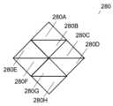
또 다른 다양한 실시예들에서, 방사는 동일한 크기의 다각형들, 동일한 형상의 다각형들, 어레이에 걸쳐 크기가 변하는 다각형들, 어레이에 걸쳐 형상이 변하는 다각형들, 펜로스 타일들(Penrose tile) 및 비반복 패턴들을 형성하는 요소들의 군으로부터 선택되는 적어도 하나를 포함하는 다양한 요소들을 사용하여 패터닝된 픽셀 어레이를 가질 수 있다.In yet other various embodiments, the emitter can have a patterned pixel array using various elements including at least one selected from the group of elements forming polygons of the same size, polygons of the same shape, polygons whose sizes vary across the array, polygons whose shapes vary across the array, Penrose tiles, and non-repeating patterns.
나아가, 다양한 실시예들은 도파관을 사용하여 이미지를 형성하기 위한 방법에 관한 것으로서, 방법은:Further, various embodiments relate to a method for forming an image using a waveguide, the method comprising:
제1 파장 대역 내의 광을 방사하는 방사 어레이, 시준 렌즈 및 제1 파장 대역 내의 S-편광된 광에 대해 회절 효율이 높은 입출력 격자들 및 제1 파장 대역 내의 P-편광된 광에 대해 회절 효율이 높은 입출력 격자들을 지지하는 도파관을 제공하는 단계;A step of providing a waveguide supporting a radiating array radiating light within a first wavelength band, a collimating lens, and input/output gratings having high diffraction efficiency for S-polarized light within the first wavelength band and input/output gratings having high diffraction efficiency for P-polarized light within the first wavelength band;
시준 렌즈를 사용하여 방사 어레이에 의해 방사된 이미지 광을 시준하는 단계;A step of collimating image light emitted by a radiation array using a collimating lens;
S-회절 입력 격자를 사용하여 OLED 어레이로부터의 이미지 변조 S-편광된 광을 도파관 내의 내부 전반사 경로 내로 커플링하는 단계;A step of coupling S-polarized light from an OLED array into an internal total reflection path within a waveguide using an S-diffraction input grating;
P-회절 입력 격자를 사용하여 OLED 어레이로부터의 이미지 변조 P-편광된 광을 도파관 내의 내부 전반사 경로 내로 커플링하는 단계;A step of coupling P-polarized light from an OLED array into an internal total reflection path within a waveguide using a P-diffraction input grating;
관찰을 위해 도파관으로부터 S-편광된 광을 빔 확대 및 추출하는 단계; 및A step of beam expanding and extracting S-polarized light from a waveguide for observation; and
관찰을 위해 도파관으로부터 P-편광된 광을 빔 확대 및 추출하는 단계를 포함한다.It includes the steps of beam expanding and extracting P-polarized light from the waveguide for observation.
또 다른 다양한 실시예들에서, 방사 어레이는 OLED 어레이일 수 있다.In yet other various embodiments, the emitter array can be an OLED array.
또 다른 다양한 실시예들에서, 본 방법은 도파관에 의해 지지되는 만곡된 광학 표면을 제공하는 단계; 방사 어레이 상의 픽셀 패턴을 사전 왜곡시키는 단계, 시준 렌즈를 사용하여 사전 왜곡된 파면들을 형성하는 단계; 만곡된 광학 표면에서 사전 왜곡된 파면 광을 반사시키는 단계; 및 만곡된 광학 표면의 광출력을 사용하여 사전 왜곡된 파면으로부터 평면 파면을 형성하는 단계를 더 포함할 수 있다.In still other various embodiments, the method may further comprise the steps of providing a curved optical surface supported by the waveguide; pre-distorting a pixel pattern on the radiating array; forming pre-distorted wavefronts using a collimating lens; reflecting the pre-distorted wavefront light from the curved optical surface; and forming a planar wavefront from the pre-distorted wavefront using the optical output of the curved optical surface.
또 다른 다양한 실시예들에서, 만곡된 광학 표면은 규정 광학 표면일 수 있다.In yet other various embodiments, the curved optical surface can be a prescribed optical surface.
본 설명은 본 발명의 하기의 도면들 및 데이터 그래프들 - 이들은 예시적인 실시예들로서 제시되고, 본 발명의 범위의 완전한 나열인 것으로서 간주되지 않아야 함 - 을 참조하여 보다 충분하게 이해될 것이다.
도 1a는 본 발명의 실시예에 따라 투명 기판 상에 증착된 단량체와 액정의 혼합물이 홀로그래픽 노출 빔들에 노출되는 표면 릴리프 격자를 제조하기 위한 방법의 단계를 개념적으로 도시한다.
도 1b는 본 발명의 실시예에 따라 투명 기판 상에 형성된 HPDLC 브래그 격자로부터 표면 릴리프 격자를 제조하기 위한 방법의 단계를 개념적으로 도시한다.
도 1c는 본 발명의 실시예에 따라 HPDLC 브래그 격자로부터 액정이 제거되어 중합체 표면 릴리프 격자를 형성하는 표면 릴리프 격자를 제조하기 위한 방법의 단계를 개념적으로 도시한다.
도 1d는 본 발명의 실시예에 따라 표면 릴리프 격자를 보호층으로 덮기 위한 방법의 단계를 개념적으로 도시한다.
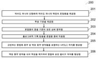
도 2는 본 발명의 실시예에 따라 투명 기판 상에 형성된 HPDLC 브래그 격자로부터 중합체 표면 릴리프 격자를 형성하기 위한 방법을 개념적으로 도시하는 흐름도이다.
도 3은 중합체 표면 릴리프 격자 또는 진공 브래그 격자의 예시적인 구현이다.
도 4a는 본 발명의 실시예에 따라 투명 기판 상에 증착된 단량체와 액정의 혼합물이 홀로그래픽 노출 빔들에 노출되는 표면 릴리프 격자를 제조하기 위한 방법의 단계를 개념적으로 도시한다.
도 4b는 본 발명의 실시예에 따라 투명 기판 상에 형성된 HPDLC 브래그 격자로부터 표면 릴리프 격자를 제조하기 위한 방법의 단계를 개념적으로 도시한다.
도 4c는 본 발명의 실시예에 따라 HPDLC 브래그 격자로부터 액정이 제거되어 중합체 표면 릴리프 격자를 형성하는 표면 릴리프 격자를 제조하기 위한 방법의 단계를 개념적으로 도시한다.
도 4d는 본 발명의 실시예에 따라 표면 릴리프 격자가 액정으로 부분적으로 재충전되어 하이브리드 표면 릴리프 브래그 격자를 형성하는 표면 릴리프 격자를 제조하기 위한 방법의 단계를 개념적으로 도시한다.
도 4e는 본 발명의 실시예에 따라 하이브리드 표면 릴리프 브래그 격자가 보호층으로 덮이는 표면 릴리프 격자를 제조하기 위한 방법의 단계를 개념적으로 도시한다.
도 5는 본 발명의 실시예에 따라 하이브리드 표면 릴리프 브래그 격자를 형성하기 위한 방법을 개념적으로 도시하는 흐름도이다.
도 6은 본 발명의 실시예에 따라 1 마이크로미터 두께의 깊은 표면 릴리프 격자에 대한 입사각에 대한 계산된 P-편광 및 S-편광 회절 효율을 도시하는 그래프이다.
도 7은 본 발명의 실시예에 따라 2 마이크로미터 두께의 깊은 표면 릴리프 격자에 대한 입사각에 대한 계산된 P-편광 및 S-편광 회절 효율을 도시하는 그래프이다.
도 8은 본 발명의 실시예에 따라 3 마이크로미터 두께의 깊은 표면 릴리프 격자에 대한 입사각에 대한 계산된 P-편광 및 S-편광 회절 효율을 도시하는 그래프이다.
도 9a 및 도 9b는 상이한 티올 농도들을 포함하는 다수의 실시예들의 주사 전자 현미경 이미지들을 예시한다.
도 10a 및 도 10b는 HPDLC 브래그 격자와 중합체 표면 릴리프 격자 또는 진공 브래그 격자를 비교한 이미지들이다.
도 11a 및 도 11b는 HPDLC 브래그 격자와 중합체 표면 릴리프 격자 또는 진공 브래그 격자를 비교한 두 개의 플롯들이다.
도 12a 및 도 12b는 상이한 깊이들을 갖는 두 개의 예시적인 중합체 표면 릴리프 격자들의 S-회절 효율 및 P-회절 효율의 두 개의 플롯들이다.
도 13a 및 도 13b는 상이한 초기 액정 농도들로 생성된 다양한 예시적인 중합체 표면 릴리프 격자들의 S-회절 효율 및 P-회절 효율의 두 개의 상이한 플롯들이다.
도 14a 및 도 14b는 상이한 초기 액정 농도들로 생성된 다양한 예시적인 중합체 표면 릴리프 격자들의 S-회절 효율 및 P-회절 효율의 두 개의 상이한 플롯들이다.
도 15는 본 발명의 실시예에 따른 도파관 디스플레이를 개념적으로 도시한다.
도 16은 본 발명의 실시예에 따른 두 개의 공기 이격된 도파관 층들을 갖는 도파관 디스플레이를 개념적으로 도시한다.
도 17은 본 발명의 실시예에 따른 도파관 디스플레이에 대한 통상적인 광선 경로들을 개념적으로 도시한다.
도 18은 본 발명의 실시예에 따라 도파관이 만곡된 광학 표면을 지지하는 도파관 디스플레이를 개념적으로 도시한다.
도 19는 본 발명의 실시예에 따라 도파관이 상부 및 하부 만곡된 광학 표면들을 지지하는 도파관 디스플레이를 개념적으로 도시한다.
도 20은 본 발명의 실시예에 따라 도파관이 만곡된 광학 표면을 지지하고 입력 이미지가 만곡된 광학 표면에 의해 도입된 수차를 보상하기 위해 사전 왜곡된 픽셀 어레이를 사용하여 제공되는 도파관 디스플레이를 개념적으로 도시한다.
도 21은 본 발명의 실시예에 따라 도파관이 만곡된 광학 표면을 지지하고 입력 이미지가 만곡된 광학 표면에 의해 도입된 수차를 보상하기 위해 만곡된 기판에 의해 지지되고 사전 왜곡된 픽셀 어레이를 사용하여 제공되는 도파관 디스플레이를 개념적으로 도시한다.
도 22는 본 발명의 실시예에 따라 S-회절 및 P-회절 격자들을 포함하는 도파관을 사용하여 관찰을 위한 이미지 광을 투사하기 위한 방법을 개념적으로 도시하는 흐름도이다.
도 23은 본 발명의 실시예에 따라 광학 규정 표면을 지지하고 S-회절 및 P-회절 격자들을 포함하는 도파관을 사용하여 관찰을 위한 이미지 광을 투사하기 위한 방법을 개념적으로 도시하는 흐름도이다.
도 24a는 본 발명의 실시예에 따른 방사 디스플레이 패널에 사용하기 위한 상이한 크기 및 종횡비의 직사각형 요소들을 갖는 픽셀 패턴의 일부를 개념적으로 도시한다.
도 24b는 본 발명의 실시예에 따른 방사 디스플레이 패널에 사용하기 위한 펜로스 타일들을 갖는 픽셀 패턴의 일부를 개념적으로 도시한다.
도 24c는 본 발명의 실시예에 따른 방사 디스플레이 패널에 사용하기 위한 육각형 요소들을 갖는 픽셀 패턴의 일부를 개념적으로 도시한다.
도 24d는 본 발명의 실시예에 따른 방사 디스플레이 패널에 사용하기 위한 정사각형 요소들을 갖는 픽셀 패턴의 일부를 개념적으로 도시한다.
도 24e는 본 발명의 실시예에 따른 방사 디스플레이 패널에 사용하기 위한 다이아몬드형 요소들을 갖는 픽셀 패턴의 일부를 개념적으로 도시한다.
도 24f는 본 발명의 실시예에 따른 방사 디스플레이 패널에 사용하기 위한 이등변 삼각형 요소들을 갖는 픽셀 패턴의 일부를 개념적으로 도시한다.
도 24g는 본 발명의 실시예에 따른 방사 디스플레이 패널에 사용하기 위한 수평 편향된 종횡비들을 갖는 육각형 요소들을 갖는 픽셀 패턴의 일부를 개념적으로 도시한다.
도 24h는 본 발명의 실시예에 따른 방사 디스플레이 패널에 사용하기 위한 수평 편향된 종횡비들을 갖는 직사각형 요소들을 갖는 픽셀 패턴의 일부를 개념적으로 도시한다.
도 24i는 본 발명의 실시예에 따른 방사 디스플레이 패널에 사용하기 위한 수평 편향된 종횡비들을 갖는 다이아몬드형 요소들을 갖는 픽셀 패턴의 일부를 개념적으로 도시한다.
도 24j는 본 발명의 실시예에 따른 방사 디스플레이 패널에 사용하기 위한 수평 편향된 종횡비의 삼각형들을 갖는 픽셀 패턴의 일부를 개념적으로 도시한다.
도 25는 본 발명의 실시예에 따라 상이한 픽셀들이 상이한 방사 특성들을 가질 수 있는 다이아몬드형 요소들을 갖는 픽셀 패턴의 일부를 개념적으로 도시한다.This description will be more fully understood by reference to the following drawings and data graphs of the present invention, which are presented as illustrative embodiments and are not to be considered as a complete clarification of the scope of the present invention.
FIG. 1a conceptually illustrates steps of a method for fabricating a surface relief grating in which a mixture of monomers and liquid crystals deposited on a transparent substrate is exposed to holographic exposure beams according to an embodiment of the present invention.
FIG. 1b conceptually illustrates steps of a method for fabricating a surface relief grating from a HPDLC Bragg grating formed on a transparent substrate according to an embodiment of the present invention.
FIG. 1c conceptually illustrates steps of a method for fabricating a surface relief grating in which liquid crystal is removed from a HPDLC Bragg grating to form a polymer surface relief grating according to an embodiment of the present invention.
FIG. 1d conceptually illustrates steps of a method for covering a surface relief grid with a protective layer according to an embodiment of the present invention.
FIG. 2 is a flow chart conceptually illustrating a method for forming a polymer surface relief grating from an HPDLC Bragg grating formed on a transparent substrate according to an embodiment of the present invention.
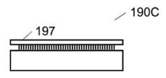
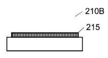
Figure 3 is an exemplary implementation of a polymer surface relief grating or vacuum Bragg grating.
FIG. 4a conceptually illustrates steps of a method for fabricating a surface relief grating in which a mixture of monomer and liquid crystal deposited on a transparent substrate is exposed to holographic exposure beams according to an embodiment of the present invention.
FIG. 4b conceptually illustrates steps of a method for fabricating a surface relief grating from a HPDLC Bragg grating formed on a transparent substrate according to an embodiment of the present invention.
FIG. 4c conceptually illustrates steps of a method for fabricating a surface relief grating in which liquid crystal is removed from a HPDLC Bragg grating to form a polymer surface relief grating according to an embodiment of the present invention.
FIG. 4d conceptually illustrates steps of a method for fabricating a surface relief grating in which the surface relief grating is partially refilled with liquid crystal to form a hybrid surface relief Bragg grating according to an embodiment of the present invention.
FIG. 4e conceptually illustrates steps of a method for fabricating a surface relief grating in which a hybrid surface relief Bragg grating is covered with a protective layer according to an embodiment of the present invention.
FIG. 5 is a flowchart conceptually illustrating a method for forming a hybrid surface relief Bragg grating according to an embodiment of the present invention.
FIG. 6 is a graph showing calculated P-polarized and S-polarized diffraction efficiencies versus incident angle for a 1 micrometer thick deep surface relief grating according to an embodiment of the present invention.
FIG. 7 is a graph showing calculated P-polarized and S-polarized diffraction efficiencies versus incident angle for a 2 micrometer thick deep surface relief grating according to an embodiment of the present invention.
FIG. 8 is a graph showing calculated P-polarized and S-polarized diffraction efficiencies versus incident angle for a 3 micrometer thick deep surface relief grating according to an embodiment of the present invention.
Figures 9a and 9b illustrate scanning electron microscopy images of multiple examples comprising different thiol concentrations.
Figures 10a and 10b are images comparing a HPDLC Bragg grating with a polymer surface relief grating or a vacuum Bragg grating.
Figures 11a and 11b are two plots comparing the HPDLC Bragg grating with a polymer surface relief grating or a vacuum Bragg grating.
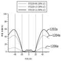
Figures 12a and 12b are two plots of the S-diffraction efficiency and the P-diffraction efficiency of two exemplary polymer surface relief gratings having different depths.
Figures 13a and 13b are two different plots of the S-diffraction efficiency and the P-diffraction efficiency of various exemplary polymer surface relief gratings generated with different initial liquid crystal concentrations.
Figures 14a and 14b are two different plots of the S-diffraction efficiency and the P-diffraction efficiency of various exemplary polymer surface relief gratings generated with different initial liquid crystal concentrations.
FIG. 15 conceptually illustrates a waveguide display according to an embodiment of the present invention.
FIG. 16 conceptually illustrates a waveguide display having two air-spaced waveguide layers according to an embodiment of the present invention.
FIG. 17 conceptually illustrates typical light paths for a waveguide display according to an embodiment of the present invention.
FIG. 18 conceptually illustrates a waveguide display supporting a curved optical surface according to an embodiment of the present invention.
FIG. 19 conceptually illustrates a waveguide display in which the waveguide supports upper and lower curved optical surfaces according to an embodiment of the present invention.
FIG. 20 conceptually illustrates a waveguide display in which the waveguide supports a curved optical surface and an input image is presented using a pre-distorted pixel array to compensate for aberrations introduced by the curved optical surface, according to an embodiment of the present invention.
FIG. 21 conceptually illustrates a waveguide display in accordance with an embodiment of the present invention in which the waveguide supports a curved optical surface and an input image is provided using a pre-distorted pixel array supported by a curved substrate to compensate for aberrations introduced by the curved optical surface.
FIG. 22 is a flowchart conceptually illustrating a method for projecting image light for observation using a waveguide including S-diffraction and P-diffraction gratings according to an embodiment of the present invention.
FIG. 23 is a flow diagram conceptually illustrating a method for projecting image light for observation using a waveguide supporting an optically regulated surface and including S-diffraction and P-diffraction gratings according to an embodiment of the present invention.
FIG. 24A conceptually illustrates a portion of a pixel pattern having rectangular elements of different sizes and aspect ratios for use in a radiant display panel according to an embodiment of the present invention.
FIG. 24b conceptually illustrates a portion of a pixel pattern having Penrose tiles for use in a radiant display panel according to an embodiment of the present invention.
FIG. 24c conceptually illustrates a portion of a pixel pattern having hexagonal elements for use in a radiant display panel according to an embodiment of the present invention.
FIG. 24d conceptually illustrates a portion of a pixel pattern having square elements for use in a radiant display panel according to an embodiment of the present invention.
FIG. 24e conceptually illustrates a portion of a pixel pattern having diamond-shaped elements for use in a radiant display panel according to an embodiment of the present invention.
FIG. 24f conceptually illustrates a portion of a pixel pattern having isosceles triangular elements for use in a radiant display panel according to an embodiment of the present invention.
FIG. 24g conceptually illustrates a portion of a pixel pattern having hexagonal elements with horizontally biased aspect ratios for use in a radiative display panel according to an embodiment of the present invention.
FIG. 24h conceptually illustrates a portion of a pixel pattern having rectangular elements with horizontally biased aspect ratios for use in a radiant display panel according to an embodiment of the present invention.
FIG. 24i conceptually illustrates a portion of a pixel pattern having diamond-shaped elements with horizontally biased aspect ratios for use in a radiant display panel according to an embodiment of the present invention.
FIG. 24J conceptually illustrates a portion of a pixel pattern having triangles of horizontally biased aspect ratio for use in a radiant display panel according to an embodiment of the present invention.
FIG. 25 conceptually illustrates a portion of a pixel pattern having diamond-shaped elements where different pixels can have different radiative characteristics according to an embodiment of the present invention.
다양한 기능들을 제공하기 위해 도파관들 상의 다양한 격자들의 사용에 대한 관심이 증가하고 있다. 이들 격자들은 각도 멀티플렉싱 격자, 컬러 멀티플렉싱 격자, 폴드 격자, 이중 상호 작용 격자, 롤링 K-벡터 격자, 교차 폴드 격자, 테셀레이트 격자(tessellated grating), 처프 격자(chirped grating), 공간적으로 변하는 굴절률 변조를 갖는 격자, 공간적으로 변하는 격자 두께를 갖는 격자, 공간적 변하는 평균 굴절률을 갖는 격자, 공간적으로 변하는 굴절률 변조 텐서를 갖는 격자, 및 공간적 변하는 평균 굴절률 텐서를 갖는 격자를 포함한다. 특정 예들에서, 광의 다양한 편광들(예를 들어, S-편광된 광 및 P-편광된 광)의 회절을 위한 격자들이 유익할 수 있다. S-편광된 광 또는 P-편광된 광 중 어느 하나를 회절시키는 격자를 갖는 것이 특히 바람직할 것이다. 이러한 기술에 대한 특정 적용예들은 증강 현실 디스플레이들 및 가상 현실 디스플레이들과 같은 도파관 기반 디스플레이들을 포함한다. 일 예는 S-편광된 광 또는 P-편광된 광 중 어느 하나 또는 양자를 도파관 내로 입력하기 위해 사용될 수 있는 입력 격자들이다. 그러나, 많은 경우에, S-편광된 광 또는 P-편광된 광 중 어느 하나를 회절시키는 격자를 갖는 것이 바람직할 것이다. 예를 들어, OLED 광원들과 같은 비편광된 광원들을 사용하는 도파관 디스플레이들은 S-편광된 광 및 P-편광된 광 양자를 생성하고, 이에 따라 S-편광된 광 및 P-편광된 광 양자를 회절시킬 수 있는 격자들을 갖는 것이 바람직할 것이다.There is growing interest in the use of various gratings on waveguides to provide a variety of functions. These gratings include angle-multiplexing gratings, color-multiplexing gratings, fold gratings, double-interaction gratings, rolling K-vector gratings, cross-fold gratings, tessellated gratings, chirped gratings, gratings with spatially varying refractive index modulation, gratings with spatially varying grating thickness, gratings with spatially varying average refractive index, gratings with spatially varying refractive index modulation tensors, and gratings with spatially varying average refractive index tensors. In certain instances, gratings that diffract different polarizations of light (e.g., S-polarized light and P-polarized light) may be beneficial. It would be particularly desirable to have a grating that diffracts either S-polarized light or P-polarized light. Specific applications for this technology include waveguide-based displays, such as augmented reality displays and virtual reality displays. An example are input gratings that can be used to input either S-polarized light or P-polarized light, or both, into the waveguide. However, in many cases it will be desirable to have a grating that diffracts either S-polarized light or P-polarized light. For example, waveguide displays that use unpolarized light sources, such as OLED light sources, generate both S-polarized light and P-polarized light, and thus it would be desirable to have gratings that can diffract both S-polarized light and P-polarized light.
격자의 하나의 특정 부류는 P-편광된 광 또는 S-편광된 광을 회절시키기 위해 사용될 수 있는 표면 릴리프 격자(surface relief grating, SRG)들을 포함한다. 또 다른 부류의 격자들은 통상적으로 P-편광 선택적인 표면 릴리프 브래그 격자(surface relief Bragg grating, SBG)들이며, 이는 유기 발광 다이오드(organic light emitting diode, OLED)들 및 발광 다이오드(LED)들과 같은 비편광된 광원들로 50% 효율 손실을 초래한다. S-편광 회절 격자와 P-편광 회절 격자들의 혼합물을 조합하면, P-회절 격자만을 사용하는 도파관들에 비해 이론적인 2x 개선을 제공할 수 있게 된다. 이에 따라, 고효율 S-편광 회절 격자를 갖는 것이 바람직할 것이다. 많은 실시예들에서, S-편광 회절 격자는 홀로그래픽 광중합체로 형성된 브래그 격자에 의해 제공될 수 있다. 일부 실시예들에서, S-편광 회절 격자는 액정(LC) 방향자들을 재정렬하기 위한 정렬층 또는 다른 공정들을 사용하여 변경된 복굴절을 갖는 홀로그래픽 중합체 분산 액정(HPDLC)으로 형성된 브래그 격자에 의해 제공될 수 있다. 몇몇 실시예들에서, S-편광 회절 격자는 상분리 하에서 S-회절 격자들로 자연적으로 조직화되는 액정들, 단량체들 및 다른 첨가제들을 사용하여 형성될 수 있다. 일부 실시예들에서, 이들 HPDLC 격자들은 우수한 S-편광 회절 효율을 갖는 깊은 SRG들을 형성할 수 있다.One particular class of gratings include surface relief gratings (SRGs), which can be used to diffract either P-polarized light or S-polarized light. Another class of gratings are surface relief Bragg gratings (SBGs), which are typically P-polarization selective, but result in a 50% efficiency loss with unpolarized light sources such as organic light emitting diodes (OLEDs) and light emitting diodes (LEDs). Combining a mixture of S-polarized and P-polarized gratings can provide a theoretical 2x improvement over waveguides using only P-polarized gratings. Accordingly, it would be desirable to have a high efficiency S-polarized grating. In many embodiments, the S-polarized grating may be provided by a Bragg grating formed of a holographic photopolymer. In some embodiments, the S-polarization diffraction grating can be provided by a Bragg grating formed of a holographic polymer dispersed liquid crystal (HPDLC) having altered birefringence using an alignment layer or other processes to realign the liquid crystal (LC) directors. In some embodiments, the S-polarization diffraction grating can be formed using liquid crystals, monomers and other additives that spontaneously organize into S-polarization gratings under phase separation. In some embodiments, these HPDLC gratings can form deep SRGs having excellent S-polarization diffraction efficiency.
깊은 SRG들의 한 부류는 높은 S-회절 효율(99%까지) 및 낮은 P-회절 효율을 보일 수 있고 도파관들을 위한 입력 격자들로서 구현될 수 있는 중합체-공기 SRG들 또는 진공 브래그 격자(evacuated Bragg grating, EBG)들이다. 이들 격자들은 액정 및 단량체 혼합물의 홀로그래픽 상분리로부터 형성된 SBG들로부터 액정을 제거함으로써 형성될 수 있다. 이러한 공정에 의해 형성된 깊은 SRG들은 통상적으로 0.35 내지 0.80 마이크로미터의 브래그 프린지 간격을 갖는 1-3 마이크로미터 범위 내의 두께를 갖는다. 일부 실시예들에서, 격자 깊이 대 브래그 프린지 간격의 비는 1:1 내지 5:1일 수 있다. 쉽게 이해될 수 있는 바와 같이, 이러한 격자들은 소정의 적용예의 특정 요건들에 따라 상이한 치수들로 형성될 수 있다. SRG들의 두께가 어떻게 상이한 결과적인 회절 효율들을 내는지의 예들은 도 6 내지 도 8과 관련하여 설명된다.A class of deep SRGs are polymer-air SRGs or evacuated Bragg gratings (EBGs), which can exhibit high S-diffraction efficiency (up to 99%) and low P-diffraction efficiency and can be implemented as input gratings for waveguides. These gratings can be formed by removing the liquid crystal from SBGs formed from the holographic phase separation of a liquid crystal and monomer mixture. Deep SRGs formed by this process typically have a thickness in the range of 1-3 micrometers with a Bragg fringe spacing of 0.35 to 0.80 micrometers. In some embodiments, the ratio of grating depth to Bragg fringe spacing can be from 1:1 to 5:1. As will be readily appreciated, these gratings can be formed with different dimensions depending on the specific requirements of a given application. Examples of how varying the thickness of the SRGs results in different resulting diffraction efficiencies are illustrated with respect to FIGS. 6-8 .
많은 실시예에서, 깊은 SRG들에 대한 조건은 높은 격자 깊이 대 프린지 간격 비를 특징으로 한다. 일부 실시예들에서, 깊은 SRG들의 형성을 위한 조건은 격자 깊이가 격자 주기의 대략 2배라는 것이다. Kogelnik 이론을 사용하여 이러한 깊은 SRG들을 모델링하는 것은 회절 효율의 합리적으로 정확한 추정치들을 제공할 수 있고, 더 진보된 모델링에 대한 필요성을 회피하며, 이는 통상적으로 Maxwell 방정식들의 수치적 해를 수반한다. HPDLC 격자들로부터의 액정 제거를 사용하여 달성될 수 있는 격자 깊이들은 깊은 SRG들(통상적으로 격자 주기 350-460 nm에 대해 250-300 nm 깊이만을 제공함)에 대한 조건을 달성할 수 없는 종래의 나노임프린트 리소그래피 방법을 사용하여 가능한 것을 크게 능가한다. (Pekka Ayras, Pasi Saarikko, Tapani Levola,” Exit pupil expander with a large field of view based on diffractive optics”, Journal of the SID 17/8, (2009), pp 659-664). S-편광 회절 깊은 SRG들이 본 출원 내에서 강조되지만, 깊은 SRG들은 후술될 바와 같이, 격자 규정의 두께, 특히 격자 깊이에 따라 편광 응답 특성들의 범위를 제공할 수 있다는 것이 여기서 강조되어야 한다. 이에 따라, 깊은 SRG들은 다양한 상이한 적용예들에서 구현될 수 있다.In many embodiments, the condition for deep SRGs is characterized by a high grating depth-to-fringe spacing ratio. In some embodiments, the condition for the formation of deep SRGs is that the grating depth is approximately twice the grating period. Modeling these deep SRGs using Kogelnik theory can provide reasonably accurate estimates of the diffraction efficiency and avoids the need for more advanced modeling, which typically involves numerical solution of Maxwell's equations. The grating depths achievable using liquid crystal ablation from HPDLC gratings significantly exceed those possible using conventional nanoimprint lithography methods, which cannot achieve the condition for deep SRGs (which typically provide only 250-300 nm depth for a grating period of 350-460 nm). (Pekka Ayras, Pasi Saarikko, Tapani Levola, “Exit pupil expander with a large field of view based on diffractive optics”, Journal of the SID 17/8, (2009), pp 659-664). Although S-polarized diffractive deep SRGs are highlighted in the present application, it should be emphasized here that deep SRGs can provide a range of polarization response characteristics depending on the thickness of the grating regulation, in particular the grating depth, as will be described below. Accordingly, deep SRGs can be implemented in a variety of different applications.
문헌은 깊은 SRG들 및 브래그 격자들의 등가성을 지지한다. 하나의 문헌(Kiyoshi Yokomori, “Dielectric surface-relief gratings with high diffraction efficiency “Applied Optics; Vol. 23; Issue 14; (1984); pp. 2303-2310)은 Maxwell 방정식을 수치적으로 풀어서 유전체 표면 릴리프 격자들의 회절 속성들의 조사를 개시한다. 격자 주기의 약 2배 깊이의 그루브 깊이를 갖는 격자의 회절 효율은 체적 위상 격자의 효율에 필적하는 것으로 밝혀졌다. Yokomori에 의한 모델링은 포토레지스트에 간섭적으로 기록된 유전체 표면 릴리프 격자들이 94%까지의 높은 회절 효율(처리 효율 85%)을 가질 수 있다고 예측하였다. 깊은 SRG들 및 브래그 격자들의 등가성은 또한 Golub의 또 다른 논문(M.A. Golub, A.A. Friesem, L. Eisen “Bragg properties of efficient surface relief gratings in the resonance domain”, Optics Communications; 235; (2004); pp261-267)은 또한 포토레지스트에서 브래그 유사 SRG들의 형성을 논의한다. Gerritsen에 의한 추가 논문은 포토레지스트에서의 브래그 유사 SRG들의 형성을 논의한다(Gerritsen HJ, Thornton DK, Bolton SR; “Application of Kogelnik's two-wave theory to deep, slanted, highly efficient, relief transmission gratings” Applied Optics; Vol. 30; Issue 7; (1991); pp 807-814).The literature supports the equivalence of deep SRGs and Bragg gratings. One article (Kiyoshi Yokomori, “Dielectric surface-relief gratings with high diffraction efficiency,” Applied Optics; Vol. 23; Issue 14; (1984); pp. 2303-2310) initiates an investigation of the diffraction properties of dielectric surface-relief gratings by numerically solving Maxwell's equations. The diffraction efficiency of a grating with a groove depth of about twice the grating period is found to be comparable to that of a volume phase grating. Modeling by Yokomori predicted that dielectric surface-relief gratings coherently written in photoresist could have diffraction efficiencies as high as 94% (with a processing efficiency of 85%). The equivalence of deep SRGs and Bragg gratings is also discussed in another paper by Golub (M.A. Golub, A.A. Friesem, L. Eisen “Bragg properties of efficient surface relief gratings in the resonance domain”, Optics Communications; 235; (2004); pp261-267). The formation of Bragg-like SRGs in photoresists is also discussed in a further paper by Gerritsen (Gerritsen HJ, Thornton DK, Bolton SR; “Application of Kogelnik's two-wave theory to deep, slanted, highly efficient, relief transmission gratings” Applied Optics; Vol. 30; Issue 7; (1991); pp 807-814).
본 개시의 많은 실시예들은 경사진 격자들을 위한 나노임프린트 리소그래피 공정 입자에 비해 매우 중요한 이점들을 제공할 수 있는 깊은 SRG들과 같은 SRG들의 제조 방법들을 제공한다. 임의의 복잡도의 브래그 격자들은 간섭 또는 마스터 및 접촉 복사 복제를 사용하여 만들어질 수 있다. 일부 실시예들에서, LC를 제거한 후에, SRG들은 LC와 상이한 속성들을 갖는 재료로 뒤채움될 수 있다. 이는 브래그 격자가 격자 형성에 필요한 격자 화학에 의해 제한되지 않는 변조 속성들을 갖도록 한다.Many embodiments of the present disclosure provide methods for fabricating SRGs, such as deep SRGs, which may offer significant advantages over nanoimprint lithography processes for angled gratings. Bragg gratings of arbitrary complexity can be fabricated using interference or master and contact copy replication. In some embodiments, after removing the LC, the SRGs can be backfilled with a material having properties different from the LC. This allows the Bragg grating to have modulation properties that are not limited by the grating chemistry required to form the grating.
일부 실시예들에서, 뒤채움 재료는 LC 재료가 아닐 수 있다. 일부 실시예들에서, 뒤채움 재료는 도파관의 각도 대역폭을 증가시킬 수 있는 공기보다 더 높은 굴절률을 가질 수 있다. 몇몇 실시예들에서, 깊은 SRG들은 하이브리드 SRG/브래그 격자를 제공하기 위해 LC로 부분적으로 뒤채움될 수 있다. 대안적으로, 일부 실시예들에서, 뒤채움 단계는 하이브리드 SRG/브래그 격자를 제공하기 위해 HPDLC의 LC 풍부 영역들로부터 LC의 일부만을 제거함으로써 회피될 수 있다. 뒤채움 접근법은 상이한 LC가 하이브리드 격자를 형성하기 위해 사용될 수 있다는 이점을 갖는다. 재료들은 잉크젯 증착 공정을 사용하여 증착될 수 있다.In some embodiments, the backfill material may not be an LC material. In some embodiments, the backfill material may have a higher refractive index than air which may increase the angular bandwidth of the waveguide. In some embodiments, the deep SRGs may be partially backfilled with LC to provide a hybrid SRG/Bragg grating. Alternatively, in some embodiments, the backfill step may be avoided by removing only a portion of the LC from the LC rich regions of the HPDLC to provide a hybrid SRG/Bragg grating. The backfill approach has the advantage that different LCs may be used to form the hybrid grating. The materials may be deposited using an inkjet deposition process.
일부 실시예들에서, 본원에서 설명되는 방법들은 광결정들을 생성하기 위해 사용될 수 있다. 광결정들은 브래그 격자들을 포함하는 다양한 회절 구조체들을 생성하도록 구현될 수 있다. 브래그 격자들은 입력 격자들, 출력 격자들, 빔 확대 격자들, 하나 이상의 원색 회절을 포함하지만 이에 제한되지 않는 기능을 제공하는 회절 격자들로서 사용될 수 있다. 광결정은 기본 브래그 격자로 달성될 수 없는 회절 능력을 가질 수 있는 3차원 격자 구조체일 수 있다. 광결정들은 모든 2D 및 3D 브라바이스 격자들을 포함하는 많은 구조체들을 포함할 수 있다. 이러한 구조체들의 기록은 두 개 이상의 기록 빔들로부터 이익을 얻을 수 있다.In some embodiments, the methods described herein can be used to create photonic crystals. The photonic crystals can be implemented to create a variety of diffractive structures, including Bragg gratings. The Bragg gratings can be used as input gratings, output gratings, beam expanding gratings, and diffractive gratings that provide functionality including but not limited to one or more primary color diffraction. The photonic crystals can be three-dimensional grating structures that can have diffractive capabilities that are not achievable with a basic Bragg grating. The photonic crystals can include many structures, including all 2D and 3D Bravais gratings. The writing of such structures can benefit from two or more writing beams.
일부 실시예들에서, 광자 결정들을 통합하는 도파관들은 도파관들의 스택들로 배열될 수 있으며, 도파관들 각각은 고유한 스펙트럼 대역폭을 회절시키기 위한 격자 규정을 갖는다. 많은 실시예들에서, 액정 추출에 의해 형성되는 광결정은 깊은 SRG를 제공한다. 많은 실시예들에서, 액정 추출 공정을 사용하여 형성되는 깊은 SRG는 통상적으로 브래그 프린지 간격이 0.35 마이크로미터 내지 0.80 마이크로미터인 1-3 마이크로미터 범위 내의 두께를 가질 수 있다. 많은 실시예에서, 깊은 SRG에 대한 조건은 높은 격자 깊이 대 프린지 간격 비를 특징으로 한다. 일부 실시예들에서, 깊은 SRG의 형성을 위한 조건은 격자 깊이가 격자 주기의 대략 2배라는 것이다. S-편광 회절 깊은 SRG들이 본 출원 내에서 주요 관심사이지만, 깊은 SRG들은 후술될 바와 같이, 격자 규정의 두께, 특히 격자 깊이에 따라 편광 응답 특성들의 범위를 제공할 수 있다는 것이 여기서 강조되어야 한다. 깊은 SRG들은 또한 도파관 디스플레이들의 색상, 균일성, 및 다른 속성들을 향상시키기 위해 종래의 브래그 격자들과 함께 사용될 수 있다.In some embodiments, the waveguides incorporating the photonic crystals may be arranged in stacks of waveguides, each of the waveguides having a grating regulation to diffract a unique spectral bandwidth. In many embodiments, the photonic crystals formed by liquid crystal extraction provide a deep SRG. In many embodiments, a deep SRG formed using a liquid crystal extraction process may have a thickness typically in the range of 1-3 micrometers with a Bragg fringe spacing of 0.35 micrometers to 0.80 micrometers. In many embodiments, a condition for a deep SRG is characterized by a high grating depth to fringe spacing ratio. In some embodiments, a condition for the formation of a deep SRG is that the grating depth is approximately twice the grating period. While S-polarization diffraction deep SRGs are of primary interest within the present application, it should be emphasized herein that deep SRGs can provide a range of polarization response characteristics depending on the thickness of the grating regulation, particularly the grating depth, as will be described below. Deep SRGs can also be used with conventional Bragg gratings to improve the color, uniformity, and other properties of waveguide displays.
깊은 SRG들은 레이저 홀로그래픽 노출을 사용하여유리질 단량체 아조벤젠 재료들로 제조되었다 (O. Sakhno, L.M. Goldenberg, M. Wegener, J. Stumpe, “Deep surface relief grating in azobenzene-containing materials using a low intensity 532 nm laser”, Optical Materials: X, 1, (2019), 100006, pp 3-7). Sakhno 문헌은 또한 SRG들이 두 개의 선형으로 직교 편광된 레이저 빔들을 사용하여 홀로그래픽 광중합체에 어떻게 기록될 수 있는지를 개시한다.Deep SRGs have been fabricated from glassy monomeric azobenzene materials using laser holographic exposure (O. Sakhno, L.M. Goldenberg, M. Wegener, J. Stumpe, “Deep surface relief grating in azobenzene-containing materials using a low intensity 532 nm laser”, Optical Materials: X, 1, (2019), 100006, pp 3-7). The Sakhno paper also discloses how SRGs can be written into holographic photopolymers using two linearly orthogonally polarized laser beams.
본 발명은 특히 경사진 격자들에 대해 나노임프린트 리소그래피 공정에 비해 매우 중요한 이점을 제공할 수 있는 표면 릴리프 격자를 제조하는 방법을 제공한다. 임의의 복잡도의 브래그 격자들은 간섭 또는 마스터 및 접촉 복사 복제를 사용하여 만들어질 수 있다. 일부 실시예들에서, LC를 제거한 후에, SRG는 LC와 상이한 속성들을 갖는 재료로 뒤채움될 수 있다. 이는 브래그 격자가 격자 형성에 필요한 격자 화학에 의해 제한되지 않는 변조 속성들을 갖도록 한다. 일부 실시예들에서, 깊은 SRG는 하이브리드 SRG/브래그 격자를 제공하기 위해 LC로 부분적으로 뒤채움될 수 있다. 대안적으로, 일부 실시예들에서, 뒤채움 단계는 하이브리드 SRG/브래그 격자를 제공하기 위해 HPDLC의 LC 풍부 영역들로부터 LC의 일부만을 제거함으로써 회피될 수 있다. 뒤채움 접근법은 상이한 LC가 하이브리드 격자를 형성하기 위해 사용될 수 있다는 이점을 갖는다. 재료들은 본 발명자들에 의한 이전의 출원들에 개시된 바와 같이 잉크젯 공정을 사용하여 증착될 수 있다. 일부 실시예들에서, 뒤채움 재료는 격자의 회절 효율을 증가시킬 수 있는 공기보다 더 높은 굴절률을 가질 수 있다.The present invention provides a method for fabricating surface relief gratings which can offer significant advantages over nanoimprint lithography processes, particularly for inclined gratings. Bragg gratings of arbitrary complexity can be fabricated using interference or master and contact copy replication. In some embodiments, after removing the LC, the SRG can be backfilled with a material having properties different from the LC. This allows the Bragg grating to have modulation properties that are not limited by the grating chemistry required for grating formation. In some embodiments, the deep SRG can be partially backfilled with LC to provide a hybrid SRG/Bragg grating. Alternatively, in some embodiments, the backfill step can be avoided by removing only a portion of the LC from the LC rich regions of the HPDLC to provide a hybrid SRG/Bragg grating. The backfill approach has the advantage that different LCs can be used to form the hybrid grating. The materials can be deposited using an inkjet process as disclosed in previous applications by the present inventors. In some embodiments, the backfill material may have a higher refractive index than air, which may increase the diffraction efficiency of the grating.
본 발명이 깊은 SRG들을 제조하는 것과 관련하여 이루어졌지만, 많은 다른 격자 구조체들이 본원에서 설명되는 기법들을 사용하여 생성될 수 있다는 것이 이해된다. 예를 들어, 격자 깊이가 격자 주파수보다 작은 SRG들(예를 들어, Raman-Nath 격자들)을 포함하는 임의의 유형의 SRG가 또한 제조될 수 있다.Although the present invention has been made with respect to fabricating deep SRGs, it is to be understood that many other grating structures may be produced using the techniques described herein. For example, any type of SRG, including SRGs having a grating depth smaller than the grating frequency (e.g., Raman-Nath gratings), may also be fabricated.
도 1a 내지 도 1d는 실시예에 따른 깊은 SRG들 또는 EBG들을 제조하기 위한 방법에서 사용될 수 있는 처리 장치를 도시한다. 도 1a는 본 발명의 실시예에 따라 투명 기판(192) 상에 증착된 단량체와 액정의 혼합물(191)이 홀로그래픽 노출 빔들(193, 194)에 노출되는 표면 릴리프 격자를 제조하기 위한 방법의 단계에서 사용될 수 있는 장치(190A)를 개념적으로 도시한다. 일부 예들에서, 혼합물은 또한 광개시제, 공개시제, 다작용성 티올, 접착 촉진제, 계면활성제, 및/또는 추가적인 첨가제들 중 적어도 하나를 포함할 수 있다. 일부 실시예들에서, 단량체는 이소시아네이트-아크릴레이트계 또는 티올렌계일 수 있다. 일부 실시예들에서, 액정은 전체 액정 혼합물 또는 전체 액정 혼합물의 일부만을 포함하는 액정 단일물일 수 있다. 액정 단일물의 다양한 예들은 시아노비페닐 또는 펜틸시아노비페닐 중 하나 또는 양자를 포함한다. 일부 실시예들에서, 액정은 노출 동안 단량체와 상분리되어 중합체 풍부 영역들 및 물질 풍부 영역들을 생성하는 또 다른 물질로 대체될 수 있다. 바람직하게는, 물질 및 액정 단일물은 후술될 바와 같은 후속 단계에서 제거되는 전체 액정 혼합물들에 대한 비용 효율적인 대체물일 수 있다.FIGS. 1A-1D illustrate a processing apparatus that may be used in a method for fabricating deep SRGs or EBGs according to an embodiment. FIG. 1A conceptually illustrates an apparatus (190A) that may be used in a step of a method for fabricating a surface relief grating in which a mixture (191) of a monomer and a liquid crystal is deposited on a transparent substrate (192) and exposed to holographic exposure beams (193, 194) according to an embodiment of the present invention. In some examples, the mixture may also include at least one of a photoinitiator, a co-initiator, a multifunctional thiol, an adhesion promoter, a surfactant, and/or additional additives. In some embodiments, the monomer may be isocyanate-acrylate based or thiolenic based. In some embodiments, the liquid crystal may be a liquid crystal monohydrate comprising the entire liquid crystal mixture or only a portion of the entire liquid crystal mixture. Various examples of the liquid crystal monohydrate include one or both of cyanobiphenyl or pentylcyanobiphenyl. In some embodiments, the liquid crystal may be replaced by another material that phase separates from the monomer during exposure to create polymer-rich regions and material-rich regions. Preferably, the material and liquid crystal single may be a cost-effective replacement for the entire liquid crystal mixtures that are removed in a subsequent step as described below.
도 1b는 본 발명의 실시예에 따라 투명 기판 상에 형성된 HPDLC 브래그 격자(195)로부터 표면 릴리프 격자를 제조하기 위한 방법의 단계에서 사용될 수 있는 장치(190B)를 개념적으로 도시한다. 홀로그래픽 노출 빔들은 일부 영역들에서 단량체를 중합체로 변형시킬 수 있다. 홀로그래픽 노출 빔들은 교차하는 기록 빔들을 포함할 수 있고, 교번하는 밝은 조명 영역 및 어두운 조명 영역을 포함할 수 있다. 중합 구동 확산 공정은 단량체 및 LC를 반대 방향들로 확산시킬 수 있으며, 이때 단량체가 겔화되어 중합체 풍부 영역들을 형성하고(밝은 영역들에서), 액정이 중합체 기질에 포획되게 되어 액정 풍부 영역들을 형성한다(어두운 영역들에서).FIG. 1B conceptually illustrates an apparatus (190B) that may be used in a step of a method for fabricating a surface relief grating from a HPDLC Bragg grating (195) formed on a transparent substrate according to an embodiment of the present invention. Holographic exposure beams may transform monomers into polymers in certain regions. The holographic exposure beams may include intersecting write beams and may include alternating brightly illuminated regions and darkly illuminated regions. A polymerization-driven diffusion process may diffuse the monomer and LC in opposite directions, wherein the monomer gels to form polymer-rich regions (in the bright regions) and the liquid crystal becomes trapped in the polymer matrix to form liquid crystal-rich regions (in the dark regions).
도 1c는 본 발명의 실시예에 따라 도 1b의 HPDLC 브래그 격자로부터 액정이 제거되어 중합체 표면 릴리프 격자를 형성하는 깊은 중합체 표면 릴리프 격자(196)를 제조하기 위한 방법의 단계에서 사용될 수 있는 장치(190C)를 개념적으로 도시한다. 바람직하게는, 중합체 표면 릴리프 격자(196)는 깊은 SRG를 형성하기 위해 비교적 작은 격자 주기를 갖는 큰 깊이를 포함할 수 있다. 액정은 이소프로필 알코올(IPA)과 같은 용매로 세척함으로써 제거될 수 있다. 용매는 액정을 씻어내기에 충분히 강해야 하지만 중합체를 유지하기에 충분히 약해야 한다. 일부 실시예들에서, 용매는 격자를 세척하기 전에 실온 미만으로 냉각될 수 있다. 도 1d는 본 발명의 실시예에 따라 중합체 표면 릴리프 브래그 격자가 보호층(197)으로 덮이는 중합체 표면 릴리프 격자를 제조하기 위한 방법의 단계에서 사용될 수 있는 장치(190D)를 개념적으로 도시한다.FIG. 1C conceptually illustrates an apparatus (190C) that can be used in a step of a method for fabricating a deep polymer surface relief grating (196) in which the liquid crystal is removed from the HPDLC Bragg grating of FIG. 1B to form a polymer surface relief grating, according to an embodiment of the present invention. Preferably, the polymer surface relief grating (196) can include a large depth with a relatively small grating period to form a deep SRG. The liquid crystal can be removed by washing with a solvent, such as isopropyl alcohol (IPA). The solvent should be strong enough to wash away the liquid crystal but weak enough to retain the polymer. In some embodiments, the solvent can be cooled to below room temperature prior to washing the grating. FIG. 1D conceptually illustrates an apparatus (190D) that can be used in a step of a method for fabricating a polymer surface relief grating in which the polymer surface relief Bragg grating is covered with a protective layer (197) according to an embodiment of the present invention.
도 2는 본 발명의 실시예에 따라 투명 기판 상에 형성된 HPDLC 브래그 격자로부터 깊은 SRG들을 형성하기 위한 방법을 개념적으로 도시한다. 도시된 바와 같이, 깊은 SRG들 또는 EBG들을 형성하는 방법(200)이 제공된다. 흐름도를 참조하면, 방법(200)은 적어도 하나의 단량체와 적어도 하나의 액정의 혼합물을 제공하는 단계(201)를 포함한다. 적어도 하나의 단량체는 이소시아네이트-아크릴레이트 단량체 또는 티올렌을 포함할 수 있다. 일부 실시예들에서, 적어도 하나의 액정은 완전 액정 혼합물일 수 있거나, 액정 혼합물의 단일 성분과 같은 액정 혼합물의 일부만을 포함할 수 있는 액정 단일물일 수 있다. 일부 실시예들에서, 적어도 하나의 액정은 노출 동안 단량체와 상분리될 수 있는 용액을 대체할 수 있다. 이러한 용액에 대한 기준들은 노출 동안 단량체와 상분리되는 능력, 경화 후 및 세척 동안 제거의 용이성, 및 취급의 용이성을 포함할 수 있다. 대체 용액의 예는 용매, 비반응성 단량체, 무기물, 및 나노입자를 포함한다.FIG. 2 conceptually illustrates a method for forming deep SRGs from HPDLC Bragg gratings formed on a transparent substrate according to an embodiment of the present invention. As illustrated, a method (200) for forming deep SRGs or EBGs is provided. Referring to the flow diagram, the method (200) includes the step of providing a mixture of at least one monomer and at least one liquid crystal (201). The at least one monomer can include an isocyanate-acrylate monomer or a thiolene. In some embodiments, the at least one liquid crystal can be a complete liquid crystal mixture, or can be a liquid crystal monolith that includes only a portion of the liquid crystal mixture, such as a single component of the liquid crystal mixture. In some embodiments, the at least one liquid crystal can replace a solution that is capable of phase separating from the monomer during exposure. Criteria for such a solution can include the ability to phase separate from the monomer during exposure, ease of removal after curing and during washing, and ease of handling. Examples of replacement solutions include solvents, non-reactive monomers, inorganics, and nanoparticles.
단량체와 액정의 혼합물을 제공하는 단계는 또한 개시제, 이를테면 광개시제 또는 공개시제, 다작용성 티올, 염료, 접착 촉진제, 계면활성제, 및/또는 추가적인 첨가제들, 이를테면 다른 가교결합제들 중 하나 이상을 적어도 하나의 단량체 및 액정과 혼합하는 단계를 포함할 수 있다. 이 혼합물은 공개시제가 단량체와 티올 사이의 반응을 촉매하도록 하기 위해 정치될 수 있다. 휴지 구간은 냉온(예를 들어, 20°C)에서 대략 8시간의 구간 동안 어두운 공간 또는 적색광(예를 들어, 적외선 광)을 갖는 공간에서 발생할 수 있다. 휴지 후, 추가적인 단량체들이 단량체 내로 혼합할 수 있다. 그 후, 이 혼합물은 작은 기공 크기(예를 들어, 0.45 ㎛ 기공 크기)를 갖는 필터를 통해 변형되거나 여과될 수 있다. 변형 후, 이 혼합물은 코팅 전에 실온에서 어두운 공간 또는 적색광을 갖는 공간 내에 저장될 수 있다.The step of providing a mixture of monomers and liquid crystals may also include mixing at least one of an initiator, such as a photoinitiator or a co-initiator, a multifunctional thiol, a dye, an adhesion promoter, a surfactant, and/or additional additives, such as other crosslinkers, with at least one of the monomers and the liquid crystal. The mixture may be allowed to settle to allow the co-initiator to catalyze the reaction between the monomers and the thiol. The resting period may occur in the dark or in a room with red light (e.g., infrared light) at a cold temperature (e.g., 20° C.) for a period of about 8 hours. After the resting period, additional monomers may be mixed into the monomers. The mixture may then be strained or filtered through a filter having a small pore size (e.g., 0.45 μm pore size). After the straining, the mixture may be stored in the dark or in a room with red light at room temperature prior to coating.
다음으로, 투명 기판이 제공될 수 있다(202). 특정 실시예들에서, 투명 기판은 유리 기판 또는 플라스틱 기판일 수 있다. 혼합물의 층이 기판의 표면 상에 증착되거나 코팅될 수 있다(203). 일부 실시예들에서, 혼합물은 내부 치수들을 유지하기 위해 유리 스페이서들을 사용하여 투명 기판과 또 다른 기판 사이에 개재된다. 비점착성 코팅이 혼합물이 개재되기 전에 다른 기판에 적용될 수 있다. 비점착성 코팅은 불소 중합체, 이를테면 OPTOOL UD509(Daikin Chemicals 제조), Dow Corning 2634, Fluoropel(Cytonix 제조), 및 EC200(PPG Industries, Inc 제조)를 포함할 수 있다. 홀로그래픽 기록 빔들이 혼합층에 적용될 수 있다(204). 홀로그래픽 기록 빔은 LC와 중합체의 상분리를 야기할 수 있는 2 빔 간섭 패턴일 수 있다. 홀로그래픽 기록 빔에 반응하여, 액체 단량체는 고체 중합체로 변화되는 반면, 중성의 비반응성 재료(예를 들어, LC)은 중합에 의해 구동되는 화학적 전위의 변화에 반응하여 홀로그래픽 노출 동안 확산된다. LC는 중성의 비반응성 물질의 일 구현예일 수 있지만, 다른 물질들도 사용될 수 있다. 물질 및 단량체는 홀로그래픽 노출 전에 혼화성 혼합물을 형성할 수 있고, 홀로그래픽 노출 시 비혼화성이 될 수 있다.Next, a transparent substrate can be provided (202). In certain embodiments, the transparent substrate can be a glass substrate or a plastic substrate. A layer of the mixture can be deposited or coated on a surface of the substrate (203). In some embodiments, the mixture is interposed between the transparent substrate and another substrate using glass spacers to maintain internal dimensions. A non-stick coating can be applied to the other substrate prior to interposing the mixture. The non-stick coating can include a fluoropolymer, such as OPTOOL UD509 (manufactured by Daikin Chemicals), Dow Corning 2634, Fluoropel (manufactured by Cytonix), and EC200 (manufactured by PPG Industries, Inc). Holographic recording beams can be applied to the mixed layer (204). The holographic recording beams can be a two-beam interference pattern that can cause phase separation of the LC and the polymer. In response to the holographic recording beam, the liquid monomer changes to a solid polymer, while the neutral, non-reactive material (e.g., LC) diffuses during the holographic exposure in response to the change in chemical potential driven by the polymerization. LC may be one embodiment of a neutral, non-reactive material, although other materials may also be used. The material and monomer may form a miscible mixture prior to the holographic exposure and may become immiscible upon the holographic exposure.
홀로그래픽 기록 빔들을 적용한 후, 혼합물은 경화될 수 있다. 경화 공정은 혼합물이 완전히 경화될 때까지 일정 시구간 동안 혼합물을 저강도 백색광 하에 두는 것을 포함할 수 있다. 저강도 백색광은 또한 광표백 염료 공정이 일어나게도 할 수 있다. 이에 따라, 교번하는 중합체 풍부 및 액정 풍부 영역들을 갖는 HPDLC 격자가 형성될 수 있다(205). 일부 실시예들에서, 경화 공정은 2시간 이내에 일어날 수 있다. 경화 후에, 기판들 중 하나가 제거되어 HPDLC 격자를 노출시킬 수 있다. 바람직하게는, 비점착성 코팅은 HPDLC 격자가 남아 있는 채로 다른 기판이 제거되도록 할 수 있다.After applying the holographic recording beams, the mixture can be cured. The curing process can include exposing the mixture under low intensity white light for a period of time until the mixture is fully cured. The low intensity white light can also cause a photobleaching dye process to occur. Accordingly, an HPDLC grating having alternating polymer-rich and liquid crystal-rich regions can be formed (205). In some embodiments, the curing process can occur within 2 hours. After curing, one of the substrates can be removed to expose the HPDLC grating. Preferably, the non-stick coating allows the other substrate to be removed while leaving the HPDLC grating behind.
HPDLC 격자는 액정 풍부 영역들 및 중합체 영역들의 교번하는 섹션들을 포함할 수 있다. 액정 풍부 영역들 내의 액정이 제거되어 깊은 SRG들로서 사용될 수 있는 중합체 표면 릴리프 격자들 또는 EBG들이 형성될 수 있다(206). 액정은 격자를 IPA와 같은 용매 내에 서서히 침지시킴으로써 제거될 수 있다. IPA는 냉각될 수 있고, 격자가 IPA 내에 침지되는 동안 실온보다 낮은 온도로 유지될 수 있다. 그 후, 격자는 용매로부터 제거되고 건조된다. 일부 실시예들에서, 격자는 압축 공기와 같은 고유량 공기원을 사용하여 건조된다. LC가 격자로부터 제거된 후, 중합체-공기 표면 릴리프 브래그 격자가 형성된다.The HPDLC grating can include alternating sections of liquid crystal rich regions and polymer regions. The liquid crystal within the liquid crystal rich regions can be removed to form polymer surface relief gratings or EBGs that can be used as deep SRGs (206). The liquid crystal can be removed by slowly immersing the grating in a solvent, such as IPA. The IPA can be cooled and maintained at a temperature below room temperature while the grating is immersed in the IPA. The grating is then removed from the solvent and dried. In some embodiments, the grating is dried using a high flow air source, such as compressed air. After the LC is removed from the grating, a polymer-air surface relief Bragg grating is formed.
도 1a 내지 도 1d에 도시된 바와 같이, 형성된 표면 릴리프 격자는 또한 보호층으로 덮일 수 있다. 일부 경우에, 보호 층은 내긁기능을 갖는 수분 및 산소 장벽일 수 있다. 일부 경우에, 보호층은 제거된 LC가 존재했던 공극 영역들을 채우지 않는 코팅일 수 있다. 코팅은 저온 공정을 사용하여 증착될 수 있다. 일부 구현들에서, 보호층은 반사 방지(AR) 속성들을 가질 수 있다. 코팅은 실리케이트 또는 실리콘 질화물일 수 있다. 코팅 공정은 나노코팅 공정과 같은 플라즈마 보조 화학 기상 증착(CVD) 공정에 의해 수행될 수 있다. 코팅은 파릴렌 코팅일 수 있다. 보호층은 유리층일 수 있다. 진공 또는 불활성 가스는 보호층이 구현되기 전에 제거된 LC가 존재했던 갭들을 채울 수 있다. 일부 실시예들에서, 코팅 공정은 LC 제거 공정과 통합될 수 있다(206). 예를 들어, 코팅 재료는 격자로부터 LC를 세척하기 위해 사용되는 용매와 혼합될 수 있다.As shown in FIGS. 1A-1D , the formed surface relief grid can also be covered with a protective layer. In some cases, the protective layer can be a moisture and oxygen barrier having scratch resistance. In some cases, the protective layer can be a coating that does not fill the void regions where the removed LC was present. The coating can be deposited using a low temperature process. In some implementations, the protective layer can have antireflective (AR) properties. The coating can be a silicate or silicon nitride. The coating process can be performed by a plasma assisted chemical vapor deposition (CVD) process, such as a nanocoating process. The coating can be a parylene coating. The protective layer can be a glass layer. A vacuum or an inert gas can fill the gaps where the removed LC was present before the protective layer is implemented. In some embodiments, the coating process can be integrated with the LC removal process (206). For example, the coating material can be mixed with a solvent used to wash the LC from the grid.
도 3은 도파관(3002) 상에 구현된 중합체-공기 표면 릴리프 브래그 격자(3000)의 예시적인 실시예의 개략적인 단면도를 도시한다. 중합체-공기 표면 릴리프 브래그 격자(3000)는 주기적인 중합체 섹션들(3004a)을 포함한다. 인접한 중합체 섹션들은 공기 섹션들(3004b)을 개재한다. 공기 섹션들(3004b)은 중합체 섹션들(3004a)에 의해 개재된다. 공기 섹션들(3004b)과 중합체 섹션들(3004a)은 상이한 굴절률들을 갖는다. 바람직하게는 중합체-공기 표면 릴리프 브래그 격자(3000)는 깊은 SRG를 생성할 수 있는 높은 격자 깊이(3006a) 대 브래그 프린지 간격(3006b) 비로 형성될 수 있다. 전술한 바와 같이, 깊은 SRG들은 통상적인 SRG들 내에 존재하지 않을 수 있는 높은 S-회절 효율과 같은 많은 유익한 품질들을 보일 수 있다.FIG. 3 illustrates a schematic cross-sectional view of an exemplary embodiment of a polymer-air surface relief Bragg grating (3000) implemented on a waveguide (3002). The polymer-air surface relief Bragg grating (3000) includes periodic polymer sections (3004a). Adjacent polymer sections are interposed between air sections (3004b). The air sections (3004b) are interposed between the polymer sections (3004a). The air sections (3004b) and the polymer sections (3004a) have different refractive indices. Preferably, the polymer-air surface relief Bragg grating (3000) can be formed with a high grating depth (3006a) to Bragg fringe spacing (3006b) ratio that can produce a deep SRG. As mentioned above, deep SRGs can exhibit many beneficial qualities such as high S-diffraction efficiency that may not be present in conventional SRGs.
일 예에서, 중합체-공기 표면 릴리프 브래그 격자(3000)는 0.35 ㎛ 내지 0.8 ㎛의 브래그 프린지 간격(3006b) 및 1 ㎛ 내지 3 ㎛ 의 격자 깊이를 가질 수 있다. 일부 실시예들에서, 중합체 섹션들(3004a)은 도 2와 관련하여 설명된 단계(206) 동안 액정이 완전히 제거되지 않을 때 적어도 일부의 잔류 액정을 포함할 수 있다. 일부 실시예들에서, 중합체 풍부 영들역 내의 잔류 LC의 존재는 최종 중합체 SRG의 굴절률 변조를 증가시킬 수 있다. 일부 실시예들에서, 공기 섹션들(3004b)은 액정이 단계(206) 동안 이들 공기 섹션들(3004b)로부터 완전히 제거되지 않는 경우 일부 잔류 액정을 포함할 수 있다. 일부 실시예들에서, 공기 섹션들(3004b) 내에 일부 잔류 액정을 남겨둠으로써, 도 4 및 도 5와 관련하여 설명된 바와 같은 하이브리드 격자가 생성될 수 있다.In one example, the polymer-air surface relief Bragg grating (3000) can have a Bragg fringe spacing (3006b) of from 0.35 μm to 0.8 μm and a grating depth of from 1 μm to 3 μm. In some embodiments, the polymer sections (3004a) can contain at least some residual liquid crystal when the liquid crystal is not completely removed during step (206) described with respect to FIG. 2. In some embodiments, the presence of residual LC within the polymer rich region can increase the refractive index modulation of the final polymer SRG. In some embodiments, the air sections (3004b) can contain some residual liquid crystal when the liquid crystal is not completely removed from these air sections (3004b) during step (206). In some embodiments, by leaving some residual liquid crystal within the air sections (3004b), a hybrid grating such as that described with respect to FIGS. 4 and 5 can be created.
상술한 바와 같이, 많은 실시예들에서, 본 발명은 또한 하이브리드 표면 릴리프/브래그 격자를 제조하기 위한 방법을 제공한다. 도 4a는 본 발명의 실시예에 따라 투명 기판(212) 상에 증착된 단량체와 액정의 혼합물(211)이 홀로그래픽 노출 빔들(213, 214)에 노출되는 하이브리드 표면 릴리프 격자들(하이브리드 SRG들)을 제조하기 위한 방법의 단계에서 사용될 수 있는 장치(210A)를 개념적으로 도시한다. 도 4b는 본 발명의 실시예에 따라 투명 기판 상에 형성된 HPDLC 브래그 격자(215)로부터 하이브리드 SRG들을 제조하기 위한 방법의 단계에서 사용될 수 있는 장치(210B)를 개념적으로 도시한다. 도 4c는 본 발명의 실시예에 따라 HPDLC 브래그 격자로부터 액정이 제거되어 중합체-공기 SRG들(216)을 형성하는 표면 릴리프 격자를 제조하기 위한 방법의 단계에서 사용될 수 있는 장치(210C)를 개념적으로 도시한다. 이들 중합체-공기 SRG들(216) 또는 EBG들은 깊은 SRG들일 수 있다. 도 4a 내지 도 4c와 관련하여 도시되고 설명되는 단계들은 중합체-공기 SRG를 생성하기 위한 공정에서 도 2a 내지 도 2c와 관련되어 도시되고 설명된 단계들에 대략 대응하고, 이에 따라 이전의 설명이 도 4a 내지 도 4c에 적용가능할 것으로 이해된다.As described above, in many embodiments, the present invention also provides a method for fabricating hybrid surface relief/Bragg gratings. FIG. 4A conceptually illustrates an apparatus (210A) that can be used in a step of a method for fabricating hybrid surface relief gratings (hybrid SRGs) in which a mixture (211) of monomer and liquid crystal is deposited on a transparent substrate (212) and exposed to holographic exposure beams (213, 214) according to an embodiment of the present invention. FIG. 4B conceptually illustrates an apparatus (210B) that can be used in a step of a method for fabricating hybrid SRGs from a HPDLC Bragg grating (215) formed on a transparent substrate according to an embodiment of the present invention. FIG. 4C conceptually illustrates an apparatus (210C) that can be used in a step of a method for fabricating surface relief gratings in which the liquid crystal is removed from the HPDLC Bragg grating to form polymer-air SRGs (216) according to an embodiment of the present invention. These polymer-air SRGs (216) or EBGs may be deep SRGs. The steps illustrated and described with respect to FIGS. 4a through 4c roughly correspond to the steps illustrated and described with respect to FIGS. 2a through 2c in the process for producing polymer-air SRGs, and thus it is understood that the previous description is applicable to FIGS. 4a through 4c.
추가적으로, 도 4d는 하이브리드 격자를 생성하기 위해 수행될 수 있는 추가적인 단계를 개념적으로 도시한다. 장치(210D)는 본 발명의 실시예에 따라, 표면 릴리프 격자가 액정으로 부분적으로 재충전되어 하이브리드 SRG들(217)을 형성하는 표면 릴리프 격자를 제조하기 위한 방법의 단계에서 사용될 수 있다. 재충전된 액정은 도 4c에서 이전에 제거되었던 이전에 제거된 액정과 상이한 일관성을 가질 수 있다. 나아가, 도 3c에서 제거된 액정은 하이브리드 SRG들(217)을 형성하는 대안적인 방법에서 단지 부분적으로 제거될 수 있는 것으로 이해된다. 추가적으로, 도 4e는 본 발명의 실시예에 따라 도 4d에 도시된 단계에서 형성된 SRG들(217)이 보호층(218)으로 덮이는 표면 릴리프 격자를 제조하기 위한 방법의 단계에서 사용될 수 있는 장치(210E)를 개념적으로 도시한다.Additionally, FIG. 4d conceptually illustrates an additional step that may be performed to create a hybrid grating. The device (210D) may be used in a step of a method for fabricating a surface relief grating in which the surface relief grating is partially refilled with liquid crystal to form hybrid SRGs (217), according to an embodiment of the present invention. The refilled liquid crystal may have a different consistency than the previously removed liquid crystal that was previously removed in FIG. 4c. Furthermore, it is understood that the liquid crystal that was removed in FIG. 3c may only be partially removed in an alternative method for forming the hybrid SRGs (217). Additionally, FIG. 4e conceptually illustrates an device (210E) that may be used in a step of a method for fabricating a surface relief grating in which the SRGs (217) formed in the step illustrated in FIG. 4d are covered with a passivation layer (218), according to an embodiment of the present invention.
도 5는 본 발명의 실시예에 따라 투명 기판 상에 형성된 HPDLC 브래그 격자로부터 하이브라드 표면 릴리프 브래그 격자를 형성하기 위한 예시적인 방법을 도시하는 흐름도이다. 도시된 바와 같이, 하이브리드 표면 릴리프 브래그 격자를 형성하는 방법(220)이 제공된다. 흐름도를 참조하면, 방법(220)은 적어도 하나의 단량체와 적어도 하나의 액정의 혼합물을 제공하는 단계(221)를 포함한다. 적어도 하나의 단량체는 이소시아네이트-아크릴레이트 단량체을 포함할 수 있다. 단량체와 액정의 혼합물을 제공하는 단계는 또한 개시제, 공개시제, 다작용성 티올, 및/또는 추가적인 첨가제들 중 하나 이상을 적어도 하나의 단량체 및 액정과 혼합하는 단계를 포함할 수 있다. 이 혼합물은 공개시제가 단량체와 티올 사이의 반응을 촉매하도록 하기 위해 정치될 수 있다. 휴지 구간은 냉온(예를 들어, 20°C)에서 대략 8시간의 구간 동안 어두운 공간 또는 적색광(예를 들어, 적외선 광)을 갖는 공간에서 발생할 수 있다. 휴지 후, 추가적인 단량체들이 단량체 내로 혼합할 수 있다. 그 후, 이 혼합물은 작은 기공 크기(예를 들어, 0.45 ㎛ 기공 크기)를 갖는 필터를 통해 변형되거나 여과될 수 있다. 변형 후, 이 혼합물은 코팅 전에 실온에서 어두운 공간 또는 적색광을 갖는 공간 내에 저장될 수 있다.FIG. 5 is a flow chart illustrating an exemplary method for forming a hybrid surface relief Bragg grating from a HPDLC Bragg grating formed on a transparent substrate according to an embodiment of the present invention. As illustrated, a method (220) for forming a hybrid surface relief Bragg grating is provided. Referring to the flow chart, the method (220) includes a step (221) of providing a mixture of at least one monomer and at least one liquid crystal. The at least one monomer can include an isocyanate-acrylate monomer. The step of providing the mixture of the monomer and the liquid crystal can also include a step of mixing one or more of an initiator, a co-initiator, a multifunctional thiol, and/or additional additives with the at least one monomer and the liquid crystal. The mixture can be allowed to stand to allow the co-initiator to catalyze the reaction between the monomer and the thiol. The resting period can occur in the dark or in a room with red light (e.g., infrared light) for a period of about 8 hours at a cold temperature (e.g., 20° C.). After the rest, additional monomers can be mixed into the monomer. The mixture can then be strained or filtered through a filter having a small pore size (e.g., 0.45 μm pore size). After straining, the mixture can be stored in a dark space or a space with red light at room temperature before coating.
다음으로, 투명 기판이 제공될 수 있다(222). 특정 실시예들에서, 투명 기판은 유리 기판 또는 플라스틱 기판일 수 있다. 비점착성 코팅이 혼합물이 기판 상에 코팅되기 전에 투명 기판에 적용될 수 있다. 혼합물의 층이 기판의 표면 상에 증착될 수 있다(223). 일부 실시예들에서, 혼합물은 내부 치수들을 유지하기 위해 유리 스페이서들을 사용하여 투명 기판과 또 다른 기판 사이에 개재된다. 홀로그래픽 기록 빔들이 혼합층에 적용될 수 있다(224). 홀로그래픽 기록 빔은 LC와 중합체의 상분리를 야기할 수 있는 2 빔 간섭 패턴일 수 있다. 홀로그래픽 기록 빔들을 적용한 후, 혼합물은 경화될 수 있다. 경화 공정은 혼합물이 완전히 경화되는 일정 시구간 동안 혼합물을 저강도 백색광 하에 두는 것을 포함할 수 있다. 저강도 백색광은 또한 광표백 염료 공정이 일어나게도 할 수 있다. 이에 따라, 교번하는 중합체 풍부 및 액정 풍부 영역들을 갖는 HPDLC 격자가 형성될 수 있다(225). 일부 실시예들에서, 경화 공정은 2시간 이내에 일어날 수 있다. 경화 후에, 기판들 중 하나가 제거되어 HPDLC 격자를 노출시킬 수 있다.Next, a transparent substrate can be provided (222). In certain embodiments, the transparent substrate can be a glass substrate or a plastic substrate. A non-stick coating can be applied to the transparent substrate prior to coating the mixture on the substrate. A layer of the mixture can be deposited on a surface of the substrate (223). In some embodiments, the mixture is interposed between the transparent substrate and another substrate using glass spacers to maintain internal dimensions. Holographic writing beams can be applied to the mixture layer (224). The holographic writing beams can be a two-beam interference pattern that can cause phase separation of the LC and the polymer. After applying the holographic writing beams, the mixture can be cured. The curing process can include exposing the mixture to low intensity white light for a period of time during which the mixture is fully cured. The low intensity white light can also cause a photobleaching dye process to occur. Accordingly, a HPDLC grating having alternating polymer-rich and liquid crystal-rich regions can be formed (225). In some embodiments, the curing process can occur within 2 hours. After curing, one of the substrates can be removed to expose the HPDLC grid.
HPDLC 격자는 액정 풍부 영역들 및 중합체 영역들의 교번하는 섹션들을 포함할 수 있다. 액정 풍부 영역들 내의 액정이 제거되어 깊은 SRG들의 형태인 중합체 표면 릴리프 격자들 또는 EBG들이 형성될 수 있다(226). 액정은 격자를 이소프로필 알콜(IPA)과 같은 용매 내에 서서히 침지시킴으로써 제거될 수 있다. IPA는 격자가 IPA 내에 침지되는 동안 더 낮은 온도로 유지될 수 있다. 그 후, 격자는 용매로부터 제거되고 건조된다. 일부 실시예들에서, 격자는 압축 공기와 같은 고유량 공기원을 사용하여 건조된다. LC가 격자로부터 제거된 후, 중합체-공기 표면 릴리프 브래그 격자가 형성된다. 도 5의 단계들(221-226)은 중합체-공기 SRG를 생성하는 것에 있어서 도 2와 관련하여 설명된 단계들에 대략 대응하고, 이에 따라 이러한 설명들은 도 5에 적용가능하다.The HPDLC grating may include alternating sections of liquid crystal rich regions and polymer regions. The liquid crystal within the liquid crystal rich regions may be removed to form polymer surface relief gratings or EBGs in the form of deep SRGs (226). The liquid crystal may be removed by slowly immersing the grating in a solvent, such as isopropyl alcohol (IPA). The IPA may be maintained at a lower temperature while the grating is immersed in the IPA. The grating is then removed from the solvent and dried. In some embodiments, the grating is dried using a high flow rate air source, such as compressed air. After the LC is removed from the grating, a polymer-air surface relief Bragg grating is formed. Steps (221-226) of FIG. 5 roughly correspond to the steps described with respect to FIG. 2 in producing a polymer-air SRG, and thus such descriptions are applicable to FIG. 5.
나아가, 방법(220)은 제거된 액정 풍부 영역들을 액정으로 적어도 부분적으로 재충전(227)하여 하이브리드 SRG들을 형성하는 단계를 포함한다. 재충전된 액정은 단계(226)에서 이전에 제거되었던 이전에 제거된 액정과 상이한 일관성을 가질 수 있다. 나아가, 단계(226)에서 제거된 액정은 하이브리드 SRG을 형성하는 대안적인 방법에서 단지 부분적으로 제거될 수 있는 것으로 이해된다. 바람직하게는 하이브리드 SRG들은 SRG들의 유익한 특정 특성들을 조정하는 기능을 제공할 수 있다. SRG들 내의 적어도 일부의 액정의 포함에 의해 개선될 수 있는 하나의 특정 특성은 탁도(haze) 속성들의 감소이다.Furthermore, the method (220) comprises a step of at least partially recharging (227) the removed liquid crystal rich regions with liquid crystal to form hybrid SRGs. The recharging liquid crystal may have a different consistency than the previously removed liquid crystal that was previously removed in step (226). Furthermore, it is understood that the liquid crystal removed in step (226) may be only partially removed in an alternative method of forming the hybrid SRGs. Preferably, the hybrid SRGs may provide the ability to tailor certain beneficial properties of the SRGs. One particular property that may be improved by the inclusion of at least a portion of liquid crystal within the SRGs is a reduction in haze properties.
도 4e에 도시된 바와 같이, 형성된 표면 릴리프 격자는 또한 보호층으로 덮일 수 있다. 일부 경우에, 보호 층은 내긁기능을 갖는 수분 및 산소 장벽일 수 있다. 일부 경우에, 보호층은 제거되었던 LC가 존재하는 공극 영역들을 충전하지 않는 코팅일 수 있다. 코팅은 저온 공정을 사용하여 증착될 수 있다. 일부 구현들에서, 보호층은 반사 방지(AR) 속성들을 가질 수 있다. 코팅은 실리케이트 또는 실리콘 질화물일 수 있다. 코팅 공정은 플라즈마처리 나노코팅 공정과 같은 플라즈마 보조 화학 기상 증착(CVD) 공정에 의해 수행될 수 있다. 코팅은 파릴렌 코팅일 수 있다. 보호층은 유리층일 수 있다. 진공 또는 불활성 가스는 보호층이 구현되기 전에 제거된 LC가 존재했던 갭들을 채울 수 있다. 일부 실시예들에서, 코팅 공정은 LC 제거 공정과 통합될 수 있다(226). 예를 들어, 코팅 재료는 격자로부터 LC를 세척하기 위해 사용되는 용매와 혼합될 수 있다. 일부 구현들에서, 코팅 재료는 중합체보다 낮거나 높은 굴절률을 갖고 인접한 중합체 부분들 사이의 공간들을 채우는 재료일 수 있다. 중합체와 코팅 재료 사이의 굴절률 차이는 중합체 SRG들이 계속해서 회절되도록 할 수 있다.As shown in FIG. 4e, the formed surface relief grid can also be covered with a protective layer. In some cases, the protective layer can be a moisture and oxygen barrier having scratch resistance. In some cases, the protective layer can be a coating that does not fill the void regions where the removed LC exists. The coating can be deposited using a low temperature process. In some implementations, the protective layer can have anti-reflective (AR) properties. The coating can be a silicate or silicon nitride. The coating process can be performed by a plasma assisted chemical vapor deposition (CVD) process, such as a plasma treated nanocoating process. The coating can be a parylene coating. The protective layer can be a glass layer. A vacuum or an inert gas can fill the gaps where the removed LC existed before the protective layer is implemented. In some embodiments, the coating process can be integrated with the LC removal process (226). For example, the coating material can be mixed with a solvent used to wash the LC from the grid. In some implementations, the coating material can be a material having a lower or higher refractive index than the polymer and filling the spaces between adjacent polymer portions. The difference in refractive index between the polymer and the coating material can cause the polymer SRGs to continue to diffract.
도 1 내지 도 5는 깊은 SRG들 및 하이브리드 표면 릴리프/브래그 격자들을 형성하기 위한 특정 방법들 및 장치를 도시하지만, 상이한 단계들 또는 이러한 단계들의 변형안들을 구현하는 다양한 제조 방법들이 이용될 수 있다. 쉽게 이해될 수 있는 바와 같이, 이용되는 특정 공정은 소정의 적용예의 특정 요건들에 따를 수 있다. 예를 들어, 많은 실시예들은 보호층으로서 또 다른 격자를 이용한다.Although FIGS. 1-5 illustrate specific methods and apparatus for forming deep SRGs and hybrid surface relief/Bragg gratings, various fabrication methods may be utilized that implement different steps or variations of these steps. As will be readily appreciated, the specific process utilized may depend upon the specific requirements of a given application. For example, many embodiments utilize another grating as a protective layer.
얕은 SRG 구조들을 갖는 하이브리드 SRG/브래그 격자들은 낮은 SRG 회절 효율을 초래할 수 있다. 본 발명에서 개시된 방법들은 브래그 격자가 효율적인 회절을 위해 충분히 두껍게 되도록 하면서 SRG들이 높은 깊이 대 격자 피치 비를 갖도록 액정 풍부 영역들 내의 액정의 깊이를 최적화함으로써 보다 효과적인 SRG 구조체들이 형성되도록 한다. 많은 실시예들에서, 하이브리드 격자의 브래그 격자 구성요소는 1-3 마이크로미터 범위 내의 두께를 가질 수 있다. 일부 실시예들에서, 하이브리드 격자의 SRG 구성요소는 0.25-3 마이크로미터 범위 내의 두께를 가질 수 있다. 초기 HPDLC 격자는 최종 SRG 및 브래그 격자 성분들의 합과 동일한 두께를 가질 것이다. 쉽게 이해될 수 있는 바와 같이, 두 개의 격자 구성요소들의 두께 비는 도파관 적용예에 따를 수 있다. 일부 실시예들에서, 격자 구조체의 각도 대역폭을 미세 조정하기 위해 SRG와 브래그 격자의 조합이 사용될 수 있다. 일부 경우에, SRG는 격자 구조체의 각도 대역폭을 증가시킬 수 있다.Hybrid SRG/Braggatings with shallow SRG structures can result in low SRG diffraction efficiency. The methods disclosed herein allow for more efficient SRG structures to be formed by optimizing the depth of the liquid crystal within the liquid crystal rich regions such that the SRGs have a high depth-to-grating pitch ratio while ensuring that the Bragg grating is thick enough for efficient diffraction. In many embodiments, the Bragg grating component of the hybrid grating can have a thickness in the range of 1-3 micrometers. In some embodiments, the SRG component of the hybrid grating can have a thickness in the range of 0.25-3 micrometers. The initial HPDLC grating will have a thickness equal to the sum of the final SRG and Bragg grating components. As will be readily appreciated, the thickness ratio of the two grating components can depend on the waveguide application. In some embodiments, a combination of SRG and Bragg grating can be used to fine-tune the angular bandwidth of the grating structure. In some cases, the SRG can increase the angular bandwidth of the grating structure.
많은 실시예들에서, 도 4a 내지 도 4e에 도시된 하이브리드 SRG들에서, 격자의 액정 영역들의 재충전 깊이는 격자에 걸쳐 변하여 공간적으로 변하는 상대적인 SRG/브래그 격자 강도들을 제공할 수 있다. 일부 실시예들에서, 단계들(206, 226, 및 227)에서 정의된 바와 같은 액정 제거 및 재충전 동안, 액정 풍부 격자 영역들 내의 액정은 전체적으로 또는 부분적으로 제거될 수 있다. 몇몇 실시예들에서, 액정 제거 영역들을 재충전하거나 부분적으로 재충전하기 위해 사용되는 액정은 초기 HPDLC 격자를 형성하기 위해 사용되는 액정과 상이한 화학 조성을 가질 수 있다. 다양한 실시예들에서, 단량체와 상용성인 상분리 속성들을 갖는 제1 액정은 최적의 변조 및 격자 정의를 갖는 HPDLC 격자를 제공하도록 지정될 수 있는 한편, 제2 재충전 액정은 최종 하이브리드 격자에서 요구되는 굴절률 변조 속성들을 제공하도록 지정될 수 있다. 다수의 실시예들에서, 하이브리드 격자의 브래그 부분은 기판 및 커버층의 표면들에 적용되는 전극들로 스위칭가능할 수 있다. 많은 실시예들에서, 재충전 액정은 스위칭 전압, 스위칭 시간, 편광, 투명도, 및 다른 파라미터들을 개선하는 특징들을 포함할 수 있지만 이에 제한되지 않는 첨가제들을 포함할 수 있다. 재충전 공정을 사용하여 형성된 하이브리드 격자는 LC가 (LC 액적의 조립체보다는) 연속체를 형성함으로써, 탁도를 감소시키는 추가의 이점들을 가질 것이다.In many embodiments, in the hybrid SRGs illustrated in FIGS. 4A-4E, the refill depth of the liquid crystal regions of the grating can be varied across the grating to provide spatially varying relative SRG/Bragg grating intensities. In some embodiments, during the liquid crystal removal and refill as defined in steps (206, 226, and 227), the liquid crystal within the liquid crystal rich grating regions can be completely or partially removed. In some embodiments, the liquid crystal used to refill or partially refill the liquid crystal removed regions can have a different chemical composition than the liquid crystal used to form the initial HPDLC grating. In various embodiments, a first liquid crystal having phase separation properties compatible with the monomer can be specified to provide a HPDLC grating having optimal modulation and grating definition, while a second refilled liquid crystal can be specified to provide the desired refractive index modulation properties in the final hybrid grating. In many embodiments, the Bragg portion of the hybrid grating can be switchable with electrodes applied to the surfaces of the substrate and cover layer. In many embodiments, the rechargeable liquid crystals may include additives that may include, but are not limited to, features that improve switching voltage, switching time, polarization, transparency, and other parameters. Hybrid gratings formed using the rechargeable process will have the additional advantage of reducing haze, as the LCs form a continuum (rather than an assembly of LC droplets).
깊은 SRG들, EBG들, 및/또는 하이브리드 SRG들이 S-회절 격자들 및 P-회절 격자들과 관련하여 설명될 수 있지만, 이들 격자들은 많은 다른 격자 유형들에의 적용가능성을 갖는다. 이들은 각도 멀티플렉싱 격자, 컬러 멀티플렉싱 격자, 폴드 격자, 이중 상호 작용 격자, 롤링 K-벡터 격자, 교차 폴드 격자, 테셀레이트 격자(tessellated grating), 처프 격자(chirped grating), 공간적으로 변하는 굴절률 변조를 갖는 격자, 공간적으로 변하는 격자 두께를 갖는 격자, 공간적 변하는 평균 굴절률을 갖는 격자, 공간적으로 변하는 굴절률 변조 텐서를 갖는 격자, 및 공간적 변하는 평균 굴절률 텐서를 갖는 격자를 포함하지만, 이에 제한되지는 않는다. 나아가, 깊은 SRG들, EBG들, 및/또는 하이브리드 SRG들은 이들의 특정 구현에 따라 스위칭가능하거나 스위칭가능하지 않은 격자들일 수 있다. 깊은 SRG들, EBG들, 및/또는 하이브리드 SRG들은 플라스틱 기판 또는 유리 기판 상에 제조될 수 있다. 이들 격자들은 또한 하나의 기판 상에 제조되고 또 다른 기판으로 전사될 수 있다.Although deep SRGs, EBGs, and/or hybrid SRGs may be described in relation to S-gratings and P-gratings, these gratings have applicability to many other grating types. These include, but are not limited to, angle-multiplexed gratings, color-multiplexed gratings, fold gratings, double-interaction gratings, rolling K-vector gratings, cross-fold gratings, tessellated gratings, chirped gratings, gratings with spatially varying refractive index modulation, gratings with spatially varying grating thickness, gratings with spatially varying average refractive index, gratings with spatially varying refractive index modulation tensors, and gratings with spatially varying average refractive index tensors. Furthermore, deep SRGs, EBGs, and/or hybrid SRGs may be switchable or non-switchable gratings depending on their particular implementation. Deep SRGs, EBGs, and/or hybrid SRGs may be fabricated on plastic substrates or glass substrates. These grids can also be fabricated on one substrate and transferred to another.
깊은 SRG들 또는 EBG들의 다양한 구현예들에 대한 논의Discussion of various implementations of deep SRGs or EBGs.
많은 실시예들에서, 깊은 SRG들은 도파관에서 편광을 제어하기 위한 수단을 제공할 수 있다. SBG들은 통상적으로 P-편광 선택적이어서, OLED들 및 LED들과 같은 비편광된 광원으로 50% 효율 손실을 초래한다. 이로 인해, S-편광 회절 격자와 P-편광 회절 격자를 조합하면, P-회절 격자만을 사용하는 도파관들에 비해 이론적인 2x 개선을 제공할 수 있게 된다. 일부 실시예들에서, S-편광 회절 격자는 종래의 홀로그래픽 광중합체로 형성된 브래그 격자에 의해 제공될 수 있다. 일부 실시예들에서, S-편광 회절 격자는 액정 방향자들을 재정렬하기 위한 정렬층 또는 다른 공정을 사용하여 변경된 복굴절을 갖는 HPDLC으로 형성된 브래그 격자에 의해 제공될 수 있다. 일부 실시예들에서, S-편광 회절 격자는 상분리 하에서 S-회절 격자들로 자연적으로 조직화되는 액정들, 단량체들 및 다른 첨가제들을 사용하여 형성될 수 있다. 많은 실시예들에서, S-편광 회절 격자는 SRG들에 의해 제공될 수 있다. 상술된 공정들을 사용하여, 높은 S-회절 효율(99%까지) 및 낮은 P-회절 효율을 보이는 깊은 SRG는 액정 및 단량체 혼합물의 홀로그래픽 상분리로부터 형성된 SBG들로부터 액정을 제거함으로써 형성될 수 있다.In many embodiments, deep SRGs may provide a means to control polarization in a waveguide. SBGs are typically P-polarization selective, resulting in a 50% efficiency loss with unpolarized light sources such as OLEDs and LEDs. Combining an S-polarization grating with a P-polarization grating may therefore provide a theoretical 2x improvement over waveguides using only a P-grating. In some embodiments, the S-polarization grating may be provided by a Bragg grating formed of a conventional holographic photopolymer. In some embodiments, the S-polarization grating may be provided by a Bragg grating formed of HPDLC having altered birefringence using an alignment layer or other process to realign the liquid crystal directors. In some embodiments, the S-polarization grating may be formed using liquid crystals, monomers, and other additives that naturally organize into S-gratings under phase separation. In many embodiments, the S-polarization diffraction grating can be provided by SRGs. Using the processes described above, deep SRGs exhibiting high S-diffraction efficiency (up to 99%) and low P-diffraction efficiency can be formed by removing the liquid crystal from the SBGs formed from the holographic phase separation of the liquid crystal and monomer mixture.
깊은 SRG들은 또한 다른 편광 응답 특성들을 제공할 수 있다. Moharam의 논문(Moharam M. G. et al. “Diffraction characteristics of photoresist surface -relief gratings”, Applied Optics, Vol. 23, p. 3214, 1984. 9. 15.)은 S와 P 감도 양자를 가지며, S가 우세한 깊은 표면 릴리프 격자들을 암시한다. 일부 실시예들에서, 깊은 SRG들은 S-편광 응답을 제공하는 능력을 실증한다. 그러나, 깊은 SRG들은 또한 다른 편광 응답 특성들을 제공할 수 있다. 많은 실시예들에서, S와 P 감도 양자 가지며 S가 우세한 깊은 표면 릴리프 격자들이 구현된다. 일부 실시예들에서, SRG의 두께는 다양한 S 및 P 회절 특성들을 제공하도록 조정될 수 있다. 몇몇 실시예들에서, 회절 효율은 스펙트럼 대역폭과 각도 대역폭에 걸쳐 P에 대해 높고, 동일한 스펙트럼 대역폭과 각도 대역폭에 걸쳐 S에 대해 낮을 수 있다. 다수의 실시예들에서, 회절 효율은 스펙트럼 대역폭과 각도 대역폭에 걸쳐 S에 대해 높고, 동일한 스펙트럼 대역폭과 각도 대역폭에 걸쳐 P에 대해 낮을 수 있다. 일부 실시예들에서, S 및 P 편광된 광 양자에 대한 높은 효율이 제공될 수 있다. 0.532 마이크론의 파장에 대해 0도 입사각 및 45도 회절각으로, 주기 0.48 마이크론의 공기 중에 침지된(이로 인해 1.3의 평균 격자 지수를 제공함) 굴절률 1.6의 SRG의 이론적인 분석이 도 5 내지 도 7에 도시되어 있다. 도 5는 본 발명의 실시예에 따라 1 마이크로미터 두께의 깊은 표면 릴리프 격자에 대한 입사각에 대한 계산된 P-편광 및 S-편광 회절 효율을 도시하는 그래프로서, 이 경우에 높은 S 및 P 응답이 달성될 수있음을 실증한다. 도 6은 본 발명의 실시예에 따라 2 마이크로미터 두께의 깊은 표면 릴리프 격자에 대한 입사각에 대한 계산된 P-편광 및 S-편광 회절 효율을 도시하는 그래프로서, 이 경우에 격자의 각도 범위의 대부분에 걸쳐 S-편광 응답이 우세함을 실증한다. 도 7은 본 발명의 실시예에 따라 3 마이크로미터 두께에 대한 입사각에 대한 계산된 P-편광 및 S-편광 회절 효율을 도시하는 그래프로서, 이 경우에 격자의 각도 범위의 상당 부분에 걸쳐 P-편광 응답이 우세함을 실증한다.Deep SRGs can also provide different polarization response characteristics. Moharam's paper (Moharam M. G. et al. “Diffraction characteristics of photoresist surface -relief gratings”, Applied Optics, Vol. 23, p. 3214, 1984. 9. 15.) suggests deep surface-relief gratings having both S and P sensitivities, with S being dominant. In some embodiments, deep SRGs demonstrate the ability to provide S-polarization response. However, deep SRGs can also provide different polarization response characteristics. In many embodiments, deep surface-relief gratings having both S and P sensitivities, with S being dominant, are implemented. In some embodiments, the thickness of the SRG can be adjusted to provide different S and P diffraction characteristics. In some embodiments, the diffraction efficiency can be high for P over the spectral and angular bandwidths, and low for S over the same spectral and angular bandwidths. In many embodiments, the diffraction efficiency can be high for S over the spectral and angular bandwidths, and low for P over the same spectral and angular bandwidths. In some embodiments, high efficiencies for both S and P polarized light can be provided. A theoretical analysis of a SRG of refractive index 1.6, immersed in air with a period of 0.48 microns (thereby providing an average grating index of 1.3), at 0 degree incidence and 45 degree diffraction angle for a wavelength of 0.532 microns is illustrated in FIGS. 5-7. FIG. 5 is a graph showing calculated P-polarized and S-polarized diffraction efficiencies versus incidence angle for a 1 micrometer thick deep surface relief grating according to an embodiment of the present invention, demonstrating that high S and P responses can be achieved in this case. FIG. 6 is a graph showing calculated P-polarization and S-polarization diffraction efficiencies versus incident angle for a 2 micrometer thick deep surface relief grating according to an embodiment of the present invention, demonstrating that the S-polarization response dominates over most of the angular range of the grating in this case. FIG. 7 is a graph showing calculated P-polarization and S-polarization diffraction efficiencies versus incident angle for a 3 micrometer thick grating according to an embodiment of the present invention, demonstrating that the P-polarization response dominates over a significant portion of the angular range of the grating in this case.
많은 실시예들에서, 광자 결정은 LC 추출 공정에 의해 형성된 반사 브래그 격자 또는 깊은 SRG일 수 있다 LC 감산이 뒤따르는 상분리를 사용하여 만들어진 반사 깊은 SRG는 넓은 각도 및 스펙트럼 대역폭을 가능하게 할 수 있다. 많은 실시예들에서, 현재 입력 SBG를 반사 광자 결정으로 대체하는 것은 화상 생성 유닛(PGU)으로부터 도파관으로의 광 경로를 감소시키기 위해 사용될 수 있다. 일부 실시예들에서, PGU 퓨필 및 도파관은 접촉할 수 있다. 많은 실시예들에서, 반사 깊이 SRG는 두께가 대략 3 마이크론일 수 있다. LC 추출 브래그 격자의 회절 속성들은 (통상적인 SRG의 경우에서와 같이 격자의 깊이로부터가 아니라) 주로 중합체와 공기 사이의 굴절률 갭으로부터 발생한다.In many embodiments, the photonic crystal may be a reflective Bragg grating formed by an LC extraction process or a deep SRG. A reflective deep SRG made using phase separation followed by LC subtraction may enable wide angular and spectral bandwidths. In many embodiments, replacing a current input SBG with a reflective photonic crystal may be used to reduce the optical path from the image generating unit (PGU) to the waveguide. In some embodiments, the PGU pupil and waveguide may be in contact. In many embodiments, the reflective deep SRG may be approximately 3 microns thick. The diffraction properties of an LC extraction Bragg grating arise primarily from the refractive index gap between the polymer and air (rather than from the depth of the grating as is the case with conventional SRGs).
초기 혼합물 내 티올 첨가제에 대한 논의Discussion of thiol additives in initial mixtures
도 9a 및 도 9b는 중합체-공기 SRG들을 제조하기 위해 사용되는 예시적인 혼합물들의 비교 산란 전자 현미경(SEM) 이미지들을 도시한다. 전술한 바와 같이, 초기 혼합물 내의 단량체는 아크릴레이트 또는 티올렌계일 수 있다. 아크릴레이트계 단량체와 같은 일부 단량체들의 경우, 홀로그래픽 노출 후, 세척 동안, 용매는 액정 재료 뿐만 아니라 이상적이지 않은 중합체를 제거하는 것으로 밝혀졌다. 다작용성 티올 첨가제는 중합체를 강화시키고 이에 따라 용매 세척을 견디기에 충분히 강하게 함으로써 이러한 문제를 해결할 수 있는 것으로 밝혀졌다. 임의의 특정 이론에 제한됨이 없이, 티올 첨가제는 감소된 가교결합으로 인해 기계적으로 약한 중합체들을 형성하는 경향이 있는 저작용성 아크릴레이트 단량체로 이루어진 제형의 기계적 강도를 개선시킬 수 있다. 아크릴레이트 단량체 제형들은 이들이 낮은 탁도와 함께 높은 회절 효율을 나타낼 수 있기 때문에 바람직할 수 있다. 이에 따라, 티올을 첨가하는 것은 아크릴레이트 단량체 형성이 중합체 SRG들의 제조에서 실행가능한 옵션이 되도록 할 수 있다.Figures 9a and 9b illustrate comparative scattering electron microscope (SEM) images of exemplary mixtures used to prepare polymer-air SRGs. As described above, the monomer in the initial mixture may be acrylate or thiolenic. For some monomers, such as acrylate monomers, it has been found that after holographic exposure, during washing, the solvent removes the liquid crystal material as well as the non-ideal polymer. It has been found that a multifunctional thiol additive can address this issue by strengthening the polymer and thus making it sufficiently strong to withstand solvent washing. Without being limited by any particular theory, it is believed that the thiol additive can improve the mechanical strength of formulations comprised of low-functionality acrylate monomers, which tend to form mechanically weak polymers due to reduced crosslinking. Acrylate monomer formulations may be desirable because they can exhibit high diffraction efficiency with low haze. Accordingly, the addition of a thiol can make acrylate monomer formulations a viable option in the preparation of polymer SRGs.
상이한 제형들 사이의 상분리, 격자 형성, 및 기계적 강도 사이에 트레이드-오프(trade-off)가 있을 수 있다. 격자 형성은 더 느리게 반응하고, 더 적은 가교를 형성하며, 홀로그래픽 노출 동안 비반응성 성분(예를 들어, LC)의 더 큰 확산을 허용하는 저작용성 단량체들을 함유하는 혼합물들로부터 이익을 얻을 수 있다. 반대로, 고작용성 단량체들로 이루어진 혼합물들은 더 큰 가교 결합으로 인해 더 양호한 상분리 및 중합체 기계적 강도를 보일 수 있지만, 비반응성 성분이 확산하기에 충분한 시간을 갖지 않아 결과적으로 더 낮은 회절 효율을 보일 수 있도록 빠르게 반응할 수 있다.There may be a trade-off between phase separation, lattice formation, and mechanical strength between different formulations. Lattice formation may benefit from blends containing lower functionality monomers that react more slowly, form fewer crosslinks, and allow greater diffusion of non-reactive components (e.g., LC) during holographic exposure. Conversely, blends comprising higher functionality monomers may exhibit better phase separation and polymer mechanical strength due to greater crosslinking, but may react so quickly that non-reactive components do not have sufficient time to diffuse, resulting in lower diffraction efficiencies.
임의의 특정 이론에 제한됨이 없이, 티올 첨가제는 아크릴레이트 또는 이소시아네이트-아크릴레이트와 반응하여 홀로그래픽 노출 전에 느슨한 스캐폴딩을 형성함으로써 이러한 제한을 받을 수 있다. 이러한 스캐폴딩은 경화된 중합체의 기계적 강도 및 균일성을 개선시킬 수 있다. 이에 따라, 기계적 강도는 단량체 혼합물의 평균 작용성을 상당히 상승시키고 격자 형성을 방해하지 않으면서 티올 작용성 및 농도의 약간의 조절을 통해 조정될 수 있다.Without being limited by any particular theory, the thiol additive may overcome these limitations by reacting with the acrylate or isocyanate-acrylate to form a loose scaffolding prior to holographic exposure. This scaffolding may improve the mechanical strength and uniformity of the cured polymer. Accordingly, the mechanical strength can be tuned by slightly adjusting the thiol functionality and concentration without significantly increasing the average functionality of the monomer mixture and interfering with lattice formation.
도 9a는 초기 혼합물을 도시하고, 도 9b는 1.5 wt% 티올을 포함하는 비교 혼합물을 도시한다. 그러나, 티올 첨가제의 다른 중량 백분율이 고려되었다. 예를 들어, 티올 첨가제의 중량 백분율은 1% 내지 4% 또는 1.5% 내지 3%일 수 있다. 일부 실시예들에서, 다작용성 티올은 트라이메틸올프로판 트리스(3-머캅토프로피오네이트)일 수 있다. 도 9a 및 도 9b 양자는 중합체 조밀 영역들(902a/902b) 및 공기 영역들(904a/904b)을 포함한다. 도시된 바와 같이, 첨가된 티올은 도 9a의 중합체 조밀 영역들(902b)보다 도 9b의 중합체 조밀 영역들(902a) 내에서 더 조밀한 중합체 구조체를 생성할 수 있으며, 이는 격자 성능을 증가시킬 수 있다. 티올 첨가제의 중량 백분율은 용매 세척을 견디도록 중합체 구조체 내에 안정성을 제공하기 위해 균형이 맞춰져야 하지만, 용매 세척 동안 액정이 방출되지 않도록 하기 위해 강성이 아닌 것으로 밝혀졌다.FIG. 9A illustrates an initial mixture and FIG. 9B illustrates a comparative mixture comprising 1.5 wt % thiol. However, other weight percentages of the thiol additive have been contemplated. For example, the weight percentage of the thiol additive can be from 1% to 4% or from 1.5% to 3%. In some embodiments, the multifunctional thiol can be trimethylolpropane tris(3-mercaptopropionate). Both FIGS. 9A and 9B include polymer dense regions (902a/902b) and air regions (904a/904b). As shown, the added thiol can create a denser polymer structure within the polymer dense regions (902a) of FIG. 9B than within the polymer dense regions (902b) of FIG. 9A, which can increase lattice performance. The weight percentage of thiol additive was found to be balanced to provide stability within the polymer structure to withstand solvent washing, but not rigidity to prevent release of the liquid crystal during solvent washing.
HPDLC 격자 성능과 중합체-공기 SRG 성능 간의 비교Comparison between HPDLC lattice performance and polymer-air SRG performance
도 10a 및 도 10b는 HPDLC 격자 및 중합체 SRG 또는 EBG의 비교예들의 이미지들을 도시한다. 도 10a는 액정이 제거되지 않은 예시적인 HPDLC 격자에 대한 성능을 도시한다. 도 10a의 격자는 공칭 또는 거의 0%의 S-회절 효율을 보이면서 20-30%의 P-회절 효율을 포함한다. 도 10b는 LC가 제거된 예시적인 중합체-공기 SRG의 성능을 도시한다. 도 10b의 격자는 51-77%의 S-회절 효율을 보이면서 18-28% P-회절 효율을 포함한다. 이에 따라, LC가 제거된 중합체-공기 SRG들은 필적할만한 P-회절 효율을 유지하면서 비교적 높은 S-회절 효율을 실증한다. 나아가, 도 10b의 격자는 0.11-0.15%의 P-회절 탁도 및 0.12-0.16%의 S-회절 탁도를 포함한다.Figures 10a and 10b illustrate images of HPDLC gratings and comparative examples of polymer SRGs or EBGs. Figure 10a illustrates the performance of an exemplary HPDLC grating with the LC removed. The grating of Figure 10a includes a P-diffraction efficiency of 20-30% while exhibiting nominal or near 0% S-diffraction efficiency. Figure 10b illustrates the performance of an exemplary polymer-air SRG with the LC removed. The grating of Figure 10b includes a P-diffraction efficiency of 18-28% while exhibiting an S-diffraction efficiency of 51-77%. Thus, the polymer-air SRGs with the LC removed demonstrate relatively high S-diffraction efficiency while maintaining comparable P-diffraction efficiency. Furthermore, the grating of Fig. 10b contains a P-diffraction haze of 0.11-0.15% and a S-diffraction haze of 0.12-0.16%.
도 11a 및 도 11b는 액정이 제거되지 않은 HPDLC 격자 및 액정이 제거된 중합체 SRG 또는 EBG의 비교예들의 플롯들을 도시한다. 도 11a는 액정이 남아 있는 HPDLC 격자에 대한 P-회절 효율 및 S-회절 효율을 도시한다. 제1 라인(1102a)은 P-회절 효율에 대응하고, 제2 라인(1104a)은 S-회절 효율에 대응한다. 도 11b는 액정이 제거된 중합체 SRG 또는 EBG에 대한 P-회절 효율 및 S-회절 효율을 도시한다. 제1 라인(1102b)은 P-회절 효율에 대응하고, 제2 라인(1104b)은 S-회절 효율에 대응한다. 도시된 바와 같이, S-회절 효율은 액정이 제거된 후에 극적으로 증가하는 한편, P-회절 효율은 비교적 유사하게 유지된다.Figures 11a and 11b show plots of comparative examples of HPDLC gratings with the liquid crystals not removed and polymer SRG or EBG with the liquid crystals removed. Figure 11a shows the P-diffraction efficiency and S-diffraction efficiency for the HPDLC grating with the liquid crystals remaining. The first line (1102a) corresponds to the P-diffraction efficiency, and the second line (1104a) corresponds to the S-diffraction efficiency. Figure 11b shows the P-diffraction efficiency and S-diffraction efficiency for the polymer SRG or EBG with the liquid crystals removed. The first line (1102b) corresponds to the P-diffraction efficiency, and the second line (1104b) corresponds to the S-diffraction efficiency. As shown, the S-diffraction efficiency increases dramatically after the liquid crystals are removed, while the P-diffraction efficiency remains relatively similar.
일부 실시예들에서, S-회절 효율 대 P-회절 효율의 비는 상이한 격자 주기들, 격자 경사각들, 및 격자 두께들을 사용함으로써 조정될 수 있다.In some embodiments, the ratio of S-diffraction efficiency to P-diffraction efficiency can be adjusted by using different grating periods, grating tilt angles, and grating thicknesses.
다양한 예시적인 깊은 SRG 깊이들Various exemplary deep SRG depths
도 12a 및 도 12b는 다양한 깊이들의 깊은 SRG들을 갖는 P-회절 및 S-회절 효율들의 다양한 비교예들을 도시한다. 이들 플롯들 각각은 회절 효율 대 각도를 나타낸다. 도 12a에서, 깊은 SRG는 대략 1.1 ㎛의 깊이를 갖는다. 제1 라인(1102a)은 S-회절 효율을 나타내고, 제2 라인(1104a)은 P-회절 효율을 나타낸다. 도시된 바와 같이, 피크 S-회절 효율은 대략 58%이고, 피크 P-회절 효율은 23%이다. 이 예에 대해, S-회절에 대한 탁도는 0.12%이고, P-회절에 대한 탁도는 0.11%임에 유의한다. 낮은 탁도를 갖는 이러한 높은 회절 효율은 멀티플렉싱된 격자들에 특히 적절한 대략 1.1 ㎛의 깊이를 갖는 깊은 SRG들을 만들 수 있다.Figures 12a and 12b illustrate various comparative examples of P-diffraction and S-diffraction efficiencies with deep SRGs of various depths. Each of these plots represents the diffraction efficiency versus angle. In Figure 12a, the deep SRG has a depth of approximately 1.1 μm. The first line (1102a) represents the S-diffraction efficiency and the second line (1104a) represents the P-diffraction efficiency. As shown, the peak S-diffraction efficiency is approximately 58% and the peak P-diffraction efficiency is 23%. Note that for this example, the haze for S-diffraction is 0.12% and the haze for P-diffraction is 0.11%. Such high diffraction efficiency with low haze can make deep SRGs having a depth of approximately 1.1 μm particularly suitable for multiplexed gratings.
도 12b에서, 깊은 SRG는 대략 1.8 ㎛의 깊이를 갖는다. 제1 라인(1102b)은 S-회절 효율을 나타내고, 제2 라인(1104b)은 P-회절 효율을 나타낸다. 도시된 바와 같이, 피크 S-회절 효율은 대략 92%이고, 피크 P-회절 효율은 63%이다. 이 예에 대해, S-회절에 대한 탁도는 0.34%이고, P-회절에 대한 탁도는 0.40%임에 유의한다. 이에 따라, S-회절 및 P-회절 효율 양자는 격자 깊이가 증가함에 따라 극적으로 증가한다. 탁도는 증가된 격자 깊이에 따라 증가하는 것으로 보인다는 점에 유의한다.In Fig. 12b, the deep SRG has a depth of approximately 1.8 μm. The first line (1102b) represents the S-diffraction efficiency, and the second line (1104b) represents the P-diffraction efficiency. As shown, the peak S-diffraction efficiency is approximately 92%, and the peak P-diffraction efficiency is 63%. Note that for this example, the turbidity for S-diffraction is 0.34%, and the turbidity for P-diffraction is 0.40%. Accordingly, both the S-diffraction and P-diffraction efficiencies increase dramatically with increasing grating depth. Note that the turbidity appears to increase with increasing grating depth.
혼합물에서의 다양한 예시적인 초기 LC 농도들Various exemplary initial LC concentrations in the mixture
도 13a 및 도 13b는 초기 혼합물에서 다양한 초기 LC 농도들을 갖는 다양한 EBG들의 비교 연구의 결과들을 도시한다. 도 13a는 S-편광 효율 대 각도를 도시한다. 도 13b는 P-편광 효율 대 각도를 도시한다. 도 13a에서, 제1 라인(1202a)은 20% 초기 LC 함량에 대응하고, 제2 라인(1204a)은 30% 초기 LC 함량에 대응하며, 제3 라인(1206a)은 40% 초기 LC 함량에 대응한다. 도 13b에서, 제1 라인(1202b)은 20% 초기 LC 함량에 대응하고, 제2 라인(1204b)은 30% 초기 LC 함량에 대응하며, 제3 라인(1206b)은 40% 초기 LC 함량에 대응한다. 표 1은 비교 연구의 다양한 결과들의 요약을 예시한다.Figures 13a and 13b illustrate the results of a comparative study of various EBGs having different initial LC concentrations in the initial mixture. Figure 13a illustrates the S-polarization efficiency versus angle. Figure 13b illustrates the P-polarization efficiency versus angle. In Figure 13a, the first line (1202a) corresponds to 20% initial LC content, the second line (1204a) corresponds to 30% initial LC content, and the third line (1206a) corresponds to 40% initial LC content. In Figure 13b, the first line (1202b) corresponds to 20% initial LC content, the second line (1204b) corresponds to 30% initial LC content, and the third line (1206b) corresponds to 40% initial LC content. Table 1 illustrates a summary of the various results of the comparative study.
S-회절 효율Maximum
S-diffraction efficiency
P-회절 효율Maximum
P-diffraction efficiency
도 13a 및 도 13b에 도시되고 표 1에 표기된 바와 같이, 최대 S-회절 및 최대 P-회절 양자는 초기 LC 함량이 높을수록 증가하는 것으로 보이는 한편, S-회절 탁도 및 P-회절 탁도는 대략 일정하게 유지된다.As illustrated in FIGS. 13a and 13b and listed in Table 1, both the maximum S-diffraction and maximum P-diffraction appear to increase with increasing initial LC content, while the S-diffraction turbidity and P-diffraction turbidity remain approximately constant.
도 14a 및 도 14b는 다양한 초기 LC 농도들에 대한 추가적인 예시적인 S-회절 및 P-회절 효율들을 도시한다. 도 14a는 다양한 초기 LC 함량들 포함하는 다양한 예시적인 EBG들에 대한 S-회절 효율을 도시한다. 도 14b는 다양한 LC 함량들 포함하는 다양한 예시적인 EBG들에 대한 P-회절 효율을 도시한다. 도 14a 및 도 14b 양자에 대해, 상단에서 하단으로 순차적으로, 라인들은: 32% LC 함량, 30% LC 함량, 28% LC 함량, 26% LC 함량, 24% LC 함량, 22% LC 함량, 및 20% LC 함량을 나타낸다. 도시된 바와 같이, S-회절 및 P-회절 효율들은 LC 함량의 양과 직접적인 관계가 있다(예를 들어, LC 함량이 높을수록 더 높은 S-회절 및 P -회절 효율들을 낸다).FIGS. 14A and 14B illustrate additional exemplary S-diffraction and P-diffraction efficiencies for various initial LC concentrations. FIG. 14A illustrates the S-diffraction efficiency for various exemplary EBGs comprising various initial LC contents. FIG. 14B illustrates the P-diffraction efficiency for various exemplary EBGs comprising various LC contents. For both FIGS. 14A and 14B, sequentially from top to bottom, the lines represent: 32% LC content, 30% LC content, 28% LC content, 26% LC content, 24% LC content, 22% LC content, and 20% LC content. As illustrated, the S-diffraction and P-diffraction efficiencies are directly related to the amount of LC content (e.g., higher LC content yields higher S-diffraction and P-diffraction efficiencies).
임의의 특정 이론에 제한되지 않고, 초기 LC 함량은 홀로그래픽 노출 공정 및 중합 공정 동안 발생하는 LC와 단량체 간의 상분리의 양과 관련된다. 이에 따라, LC 함량이 높을수록 세척 후 더 많은 공기 영역들을 만들기 위해 제거되는 LC 풍부 영역들의 양이 증가될 것이다. 증가된 공기 영역들은 공기 영역들(이전에는 액정 풍부 영역들)과 중합체 풍부 영역들 사이의 굴절률 차이(Δn)를 더 크게 만들며, 이는 S-회절 및 P-회절 효율 양자를 증가시킨다. 일부 실시예들에서, 중합체 SRG들의 평균 굴절률은 초기 중성 물질(예를 들어, LC) 함량을 조정함으로써 조정될 수 있으며, 이에 의해 중성 물질의 제거 후 중합체의 부피를 증가시키거나 감소시킨다. 나아가, 초기 중성 물질 함량을 증가시키는 것은 기계적 강도에 영향을 줄 수 있다. 이에 따라, 티올 첨가제와 같은 기계적 강도 증강제의 증가 또는 감소가 기계적 강도의 증가 또는 감소의 균형을 맞추기 위해 사용될 수 있다.Without being limited to any particular theory, the initial LC content is related to the amount of phase separation between the LC and monomer that occurs during the holographic exposure process and the polymerization process. Accordingly, a higher LC content will increase the amount of LC rich regions that are removed to create more air regions after washing. The increased air regions create a larger difference in refractive index (Δn) between the air regions (formerly the LC rich regions) and the polymer rich regions, which increases both the S-diffraction and P-diffraction efficiencies. In some embodiments, the average refractive index of the polymer SRGs can be adjusted by adjusting the initial neutral (e.g., LC) content, thereby increasing or decreasing the volume of the polymer after removal of the neutral. Furthermore, increasing the initial neutral content can affect the mechanical strength. Accordingly, increasing or decreasing a mechanical strength enhancing agent, such as a thiol additive, can be used to balance the increase or decrease in mechanical strength.
이미지 생성기들로서 OLED 어레이들을 포함하는 실시예들Embodiments including OLED arrays as image generators
도파관 디스플레이들에서 이미지 생성기들로서 유기 발광 다이오드(OLED) 어레이들의 사용에 대한 관심이 증가하고 있다. OLED들은 도파관 디스플레이 적용예들에서 많은 이점들을 갖는다. 발광 기술로서, OLED들은 광원을 필요로 하지 않는다. OLED들은 대면적에 걸쳐 비용 효율적으로 인쇄될 수 있다. 비직사각형 픽셀 어레이 패턴들이 곡선형 또는 가요성 기판 상에 인쇄될 수 있다. 후술될 바와 같이, 픽셀 어레이를 사전 왜곡하고 곡선형 초점면을 생성하는 능력은 도파관에 의해 지지되는 곡선형 도파관들 및 처방 렌즈들에 의해 야기되는 가이드되는 빔 파면 왜곡들에 대한 보상을 가능하게 할 수 있는 새로운 설계 치수를 추가한다. 4Kx4K 픽셀들의 해상도들을 갖는 OLED들은 LCoS(Liquid Crystal on Silicon) 및 디지털 라이트 프로세싱(digital light processing, DLP) 디바이스들과 같은 미세 전자 기계 시스템(Micro Electro Mechanical Systems, MEMS) 디바이스들 같은 기술들에 의해 제공될 수 있는 것보다 높은 해상도, 넓은 FOV AR 디스플레이들에 대한 더 빠른 루트를 제공하여, 근거리에서 더 높은 해상도의 양호한 전망들과 현재 이용가능하다. LCoS에 비해 또 다른 중요한 이점은 OLED들이 (LC 디바이스들에 대한 밀리초와 비교하여) 마이크로초로 스위칭할 수 있다는 것이다.There is growing interest in the use of organic light emitting diode (OLED) arrays as image generators in waveguide displays. OLEDs have many advantages in waveguide display applications. As a light emitting technology, OLEDs do not require a light source. OLEDs can be cost-effectively printed over large areas. Non-rectangular pixel array patterns can be printed on curved or flexible substrates. As described below, the ability to pre-distort the pixel array and create a curved focal plane adds a new design dimension that can enable compensation for guided beam wavefront distortions caused by curved waveguides and prescription lenses supported by the waveguide. OLEDs with resolutions of 4Kx4K pixels offer a faster route to higher resolution, wide FOV AR displays than can be provided by technologies such as Micro Electro Mechanical Systems (MEMS) devices such as Liquid Crystal on Silicon (LCoS) and digital light processing (DLP) devices, with good prospects for higher resolution at close range and currently available. Another important advantage over LCoS is that OLEDs can switch in microseconds (compared to milliseconds for LC devices).
OLED들은 특정 단점들을 갖는다. 이들의 기본 형태에서, OLED들은 램버시안 이미터(Lambertian emitter)들이며, 이는 효율적인 광 수집을 LCoS 및 DLP 마이크로 디스플레이들보다 훨씬 더 훨씬 더 어렵게 한다. OLED들의 적색, 녹색, 및 청색 스펙트럼 대역폭들은 발광 다이오드(LED)들의 스펙트럼 대역폭보다 더 넓어서, 홀로그래픽 도파관들에서의 추가의 광 관리 문제들을 제시한다. OLED들의 가장 중요한 단점은 P-편광 선택적 경향이 있는 스위칭가능한 브래그 격자(SBG)들과 같은 HPDLC 격자들을 사용하는 도파관들에서, OLED로부터 이용가능한 광의 절반이 낭비된다는 점이다. 이에 따라, 본 발명의 많은 실시예들은 비편광된 광에 대해 높은 광 효율을 제공할 수 있는 방사 비편광 이미지 소스들과 사용하기 위한 도파관 디스플레이들 및 이러한 도파관 디스플레이들을 제조하는 관련 방법들에 관한 것이다.OLEDs have certain drawbacks. In their basic form, OLEDs are Lambertian emitters, which makes efficient light collection much more difficult than LCoS and DLP microdisplays. The red, green, and blue spectral bandwidths of OLEDs are wider than the spectral bandwidth of light emitting diodes (LEDs), presenting additional light management challenges in holographic waveguides. A major drawback of OLEDs is that in waveguides using HPDLC gratings, such as switchable Bragg gratings (SBGs), which tend to be P-polarization selective, half of the available light from the OLED is wasted. Accordingly, many embodiments of the present invention relate to waveguide displays for use with radiative unpolarized image sources that can provide high optical efficiency for unpolarized light, and related methods of fabricating such waveguide displays.
실시예들을 설명하기 위해, 광학적 설계 및 시각적 디스플레이들의 당업자들에게 알려져 있는 광학 기술의 일부 잘 알려져 있는 특징들은 본 발명의 기본 원리들을 모호하게 하지 않기 위해 생략되거나 간략화되었다. 달리 언급되지 않는 한, 광선 또는 빔 방향에 관한 용어 "축상(on-axis)"은 본 발명과 관련하여 설명되는 광학 구성요소들의 표면들에 수직인 축에 평행한 전파를 지칭한다. 하기의 설명에서, 용어 광, 광선, 빔, 및 방향은 직선 궤적들에 따른 전자기 방사선의 전파 방향을 나타내기 위해 서로 호환하여 그리고 연관되어 사용될 수 있다. 용어 광 및 조사는 전자기 스펙트럼의 가시 및 적외선 대역들과 관련하여 사용될 수 있다. 하기의 설명의 부분들은 광학 설계 분야의 당업자들에 의해 통용되는 용어를 사용하여 제시될 것이다. 본원에서 사용될 때, 용어 격자는 일부 실시예들에서 격자들의 세트로 구성되는 격자를 포괄할 수 있다. 예시를 위해, 도면들은 달리 언급되지 않는 한 일정한 축척으로 도시되지 않음을 이해해야 한다.For the purpose of describing the embodiments, some well-known features of optical technology known to those skilled in the art of optical design and visual displays have been omitted or simplified so as not to obscure the basic principles of the present invention. Unless otherwise stated, the term "on-axis" with respect to light or beam direction refers to propagation parallel to an axis perpendicular to the surfaces of the optical components described in connection with the present invention. In the following description, the terms light, light, beam, and direction may be used interchangeably and in conjunction with each other to refer to the direction of propagation of electromagnetic radiation along straight-line trajectories. The terms light and radiation may be used in reference to the visible and infrared bands of the electromagnetic spectrum. Portions of the following description will be presented using terminology commonly used by those skilled in the art of optical design. As used herein, the term grating may encompass a grating comprised of a set of gratings in some embodiments. It should be understood that for purposes of illustration, the drawings are not drawn to scale unless otherwise stated.
이제 도면들을 참조하면, 본 발명의 다양한 실시예들에 따라 발광 입력 이미지 패널들을 사용하여 도파관 디스플레이들을 제공하기 위한 방법들 및 장치가 도시된다. 도 15는 본 발명의 실시예에 따른 도파관 디스플레이를 개념적으로 도시한다. 도시된 바와 같이, 장치(100)는 제1 파장 대역 내의 P-편광된 광에 대해 회절 효율이 높은 입력(102) 및 출력(103) 격자들 및 제1 파장 대역 내의 S-편광된 광에 대해 회절 효율이 높은 입력(104) 및 출력(105) 격자들을 지지하는 도파관(101)을 포함한다.Referring now to the drawings, methods and apparatus for providing waveguide displays using luminescent input image panels according to various embodiments of the present invention are illustrated. FIG. 15 conceptually illustrates a waveguide display according to an embodiment of the present invention. As illustrated, the apparatus (100) includes a waveguide (101) supporting input (102) and output (103) gratings having high diffraction efficiency for P-polarized light within a first wavelength band and input (104) and output (105) gratings having high diffraction efficiency for S-polarized light within the first wavelength band.
장치(100)는 제1 파장 대역을 포함하는 방사 스펙트럼 대역폭을 갖는 비편광된 광을 방사하는 OLED 마이크로디스플레이(106), 및 OLED 마이크로 디스플레이로부터 시야 내로 광을 투사하기 위한 시준 렌즈(107)를 더 포함한다. 예시적인 실시예에서, S 및 P 회절 격자들(102-105)은 에어 갭이 요구되지 않고 적층될 수 있다. 다른 실시예들에서, 격자 층들은 에어 갭 또는 투명 층에 의해 분리될 수 있다. S 및 P 회절 격자들(102 내지 105)은 상술된 깊은 SRG들 또는 EBG들일 수 있다.The device (100) further includes an OLED microdisplay (106) emitting unpolarized light having an emission spectral bandwidth including a first wavelength band, and a collimating lens (107) for projecting light from the OLED microdisplay into a field of view. In an exemplary embodiment, the S and P diffraction gratings (102-105) can be stacked without requiring an air gap. In other embodiments, the grating layers can be separated by an air gap or a transparent layer. The S and P diffraction gratings (102-105) can be the deep SRGs or EBGs described above.
도 16은 P-회절 및 S-회절 격자들이 별도의 공기 이격된 도파관 층들에 배치된 본 발명의 실시예에 따른 도파관 디스플레이를 개념적으로 도시한다. 도시된 바와 같이, 장치(110)는 에어 갭(113)에 의해 분리된 (격자들(102, 103 및 104, 105)을 각각 지지하는) 상부(111) 및 하부(112) 도파관 층들을 포함한다. 격자들(102, 103 및 104, 105)은 상술한 깊은 SRG들 및 EBG들일 수 있다.FIG. 16 conceptually illustrates a waveguide display according to an embodiment of the present invention in which P- and S-diffraction gratings are arranged in separate air-spaced waveguide layers. As illustrated, the device (110) includes upper (111) and lower (112) waveguide layers (supporting gratings (102, 103 and 104, 105) respectively) separated by an air gap (113). The gratings (102, 103 and 104, 105) can be the deep SRGs and EBGs described above.
도 17은 본 발명의 실시예에 따른 도파관 디스플레이에서의 통상적인 광선 경로들을 개념적으로 도시한다. 도 17에 도시된 실시예(120)에서, 마이크로디스플레이(106)는 제1 파장 대역 내의 비편광된 광(121)을 방사하도록 구성되며, 이는 이는 시준기 렌즈(107)에 의해 시야 내로 시준되고 투사된다. 마이크로디스플레이(106)로부터의 S-편광된 방사는 S-회절 입력 격자(104)에 의해 도파관(101) 내의 내부 전반사 경로로 인커플링될 수 있고, S-회절 출력 격자(105)에 의해 도파관(101)으로부터 추출될 수 있다. 마이크로디스플레이(106)로부터의 P-편광된 광은 유사한 방식으로 P-회절 입력 및 출력 격자들(102, 103)을 사용하여 인커플링되고 추출될 수 있다. 분산은 입력 및 출력 격자 공간 주파수들이 정합된다면 S 및 P 광 양자에 대해 보정될 수 있다. 입력 및 출력 격자들(102, 103)은 상술한 깊은 SRG들 또는 EBG들일 수 있다.FIG. 17 conceptually illustrates typical light paths in a waveguide display according to an embodiment of the present invention. In the embodiment (120) illustrated in FIG. 17, the microdisplay (106) is configured to emit unpolarized light (121) within a first wavelength band, which is collimated and projected into the field of view by a collimator lens (107). S-polarized radiation from the microdisplay (106) can be incoupled into an internal total reflection path within the waveguide (101) by the S-diffraction input grating (104) and extracted from the waveguide (101) by the S-diffraction output grating (105). P-polarized light from the microdisplay (106) can be incoupled and extracted in a similar manner using the P-diffraction input and output gratings (102, 103). Dispersion can be corrected for both the S and P light if the input and output grating spatial frequencies are matched. The input and output grids (102, 103) can be the deep SRGs or EBGs described above.
도 15 내지 도 17은 특정 도파관 디스플레이 구성들을 도시하지만, 도시된 것들에 대한 수정을 포함하는 다양한 구성들이 구현될 수 있으며, 이의 특정 구현은 소정의 적용예의 특정 요건들에 따를 수 있다. 더 나아가, 이러한 디스플레이들은 다수의 상이한 방법들을 사용하여 제조될 수 있다. 예를 들어, 많은 실시예들에서, 두 개의 격자 층들이 잉크젯 인쇄 공정을 사용하여 형성된다.While FIGS. 15-17 illustrate specific waveguide display configurations, various configurations including modifications to those illustrated may be implemented, the particular implementation of which may depend on the particular requirements of a given application. Furthermore, such displays may be manufactured using a number of different methods. For example, in many embodiments, the two grating layers are formed using an inkjet printing process.
많은 실시예들에서, 도파관은 단색 대역에서 동작한다. 일부 실시예들에서, 도파관은 녹색 대역에서 동작한다. 몇몇 실시예들에서, 적색, 녹색 및 청색(RGB)과 같은 상이한 스펙트럼 대역들에서 동작하는 도파관 층들이 3층 도파 구조체를 제공하기 위해 적층될 수 있다. 추가 실시예들에서, 층들에는 도파관 층들 사이에 에어 갭들이 적층된다. 다양한 실시예들에서, 도파관 층들은 두 개의 도파관 층 솔루션들을 제공하기 위해 청색-녹색 및 녹색-적색과 같은 더 넓은 대역들에서 동작한다. 다른 실시예들에서, 격자들은 격자층들의 수를 감소시키기 위해 컬러 멀티플렉싱된다. 다양한 타입들의 격자들이 구현될 수 있다. 일부 실시예들에서, 각 층 내의 적어도 하나의 격자는 스위칭 가능한 격자이다.In many embodiments, the waveguide operates in a monochromatic band. In some embodiments, the waveguide operates in the green band. In some embodiments, waveguide layers operating in different spectral bands, such as red, green, and blue (RGB), may be stacked to provide a three-layer waveguide structure. In further embodiments, the layers have air gaps stacked between the waveguide layers. In various embodiments, the waveguide layers operate in broader bands, such as blue-green and green-red, to provide two waveguide layer solutions. In other embodiments, the gratings are color multiplexed to reduce the number of grating layers. Various types of gratings may be implemented. In some embodiments, at least one grating within each layer is a switchable grating.
본 발명은 문헌에 개시된 것들을 포함하는 다양한 도파관 아키텍처들을 사용하여 적용될 수 있다. 많은 실시예들에서, 도파관은 각도 멀티플렉싱 격자, 컬러 멀티플렉싱 격자, 폴드 격자, 이중 상호 작용 격자, 롤링 K-벡터 격자, 교차 폴드 격자, 테셀레이트 격자(tessellated grating), 처프 격자(chirped grating), 공간적으로 변하는 굴절률 변조를 갖는 격자, 공간적으로 변하는 격자 두께를 갖는 격자, 공간적 변하는 평균 굴절률을 갖는 격자, 공간적으로 변하는 굴절률 변조 텐서를 갖는 격자, 및 공간적 변하는 평균 굴절률 텐서를 갖는 격자 중 적어도 하나를 통합할 수 있다. 일부 실시예들에서, 도파관은 반파장판, 1/4파장판, 반사 방지 코팅, 빔 스플리팅 층, 정렬 층, 섬광 감소를 위한 광색성 배면 층, 섬광 감소를 위한 루버 막 중 적어도 하나를 포함할 수 있다. 몇몇 실시예들에서, 도파관은 상이한 편광들에 대한 개별 광 경로들을 제공하는 격자들을 지지할 수 있다. 다양한 실시예들에서, 도파관은 상이한 스펙트럼 대역폭들에 대한 개별 광 경로들을 제공하는 격자들을 지지할 수 있다. 다수의 실시예들에서, 본 발명에서 사용하기 위한 격자들은 HPDLC 격자, HPDLC에 기록되는 스위칭 격자(상기한 스위칭 가능한 브래그 격자), 홀로그래픽 광중합체에 기록되는 브래그 격자, 또는 표면 릴리프 격자일 수 있다.The present invention can be applied using a variety of waveguide architectures, including those disclosed in the literature. In many embodiments, the waveguide can incorporate at least one of an angular multiplexing grating, a color multiplexing grating, a fold grating, a double interaction grating, a rolling K-vector grating, a cross-fold grating, a tessellated grating, a chirped grating, a grating with spatially varying refractive index modulation, a grating with spatially varying grating thickness, a grating with spatially varying average refractive index, a grating with a spatially varying refractive index modulation tensor, and a grating with a spatially varying average refractive index tensor. In some embodiments, the waveguide can include at least one of a half-wave plate, a quarter-wave plate, an anti-reflection coating, a beam-splitting layer, an alignment layer, a photochromic backing layer for glare reduction, and a louvered film for glare reduction. In some embodiments, the waveguide can support gratings that provide separate optical paths for different polarizations. In various embodiments, the waveguide may support gratings that provide individual optical paths for different spectral bandwidths. In many embodiments, the gratings for use in the present invention may be a HPDLC grating, a switchable grating written in HPDLC (a switchable Bragg grating as described above), a Bragg grating written in a holographic photopolymer, or a surface relief grating.
많은 실시예들에서, 도파관 디스플레이는 적어도 50° 대각선의 이미지 관찰 시야를 제공할 수 있다. 추가 실시예들에서, 도파관 디스플레이는 적어도 70° 대각선의 이미지 관찰 시야를 제공할 수 있다. 일부 실시예들에서, OLED 디스플레이는 4000 니트보다 큰 휘도 및 4kx4k 픽셀의 해상도를 가질 수 있다. 몇몇 실시예들에서, 도파관은 휘도 4000 니트의 OLED 디스플레이를 사용하여 400 니트보다 큰 이미지 휘도가 제공될 수 있도록 10%보다 큰 광학 효율을 가질 수 있다. P-회절 격자들을 구현하는 도파관 디스플레이들은 통상적으로 5% - 6.2%의 도파관 효율을 갖는다. 상술한 바와 같이 S-회절 격자들을 제공하는 것은 도파관의 효율을 2배 증가시킬 수 있다. 다양한 실시예들에서, 25 mm보다 큰 아이 릴리프(eye relief)를 갖는 10 mm보다 큰 아이 박스가 제공될 수 있다. 많은 실시예들에서, 도파관 두께는 2.0-5.0 mm 사이일 수 있다.In many embodiments, the waveguide display can provide an image viewing field of view of at least 50° diagonal. In further embodiments, the waveguide display can provide an image viewing field of view of at least 70° diagonal. In some embodiments, the OLED display can have a brightness greater than 4000 nits and a resolution of 4kx4k pixels. In some embodiments, the waveguide can have an optical efficiency greater than 10% such that an image brightness greater than 400 nits can be provided using an OLED display having a brightness of 4000 nits. Waveguide displays implementing P-diffraction gratings typically have a waveguide efficiency of 5% - 6.2%. Providing S-diffraction gratings as described above can double the efficiency of the waveguide. In various embodiments, an eye box greater than 10 mm with an eye relief greater than 25 mm can be provided. In many embodiments, the waveguide thickness may be between 2.0-5.0 mm.
도 18은 도파관 광학 표면들 중 적어도 하나의 적어도 일부가 만곡되고 사이드 빔 파면들에 대한 만곡된 표면 부분의 효과가 있는 본 발명의 실시예에 따른 도파관 디스플레이를 개념적으로 도시한다. 도시된 바와 같이, 장치(130)는 곡면부(132)를 지지하는 도파관(131)을 포함한다. 예시적인 실시예에서, 도파관(131)은 제1 파장 대역 내의 P-편광된 광에 대해 회절 효율이 높은 입력(102) 및 출력(103) 격자들 및 제1 파장 대역 내의 S-편광된 광에 대해 회절 효율이 높은 입력(104) 및 출력(105) 격자들을 지지한다. 픽셀들(133)의 직사각형 어레이를 디스플레이하는 마이크로디스플레이(106)는 제1 파장 대역 내의 비편광된 광(134)을 방사하며, 이는 시준 렌즈(107)에 의해 시준되어 시야 내로 투사된다. 마이크로디스플레이(106)로부터의 P-편광된 방사는 P-회절 입력 격자(102)에 의해 도파관 내의 내부 전반사 경로로 인커플링될 수 있고, P-회절 출력 격자(103)에 의해 도파관으로부터 추출될 수 있다. 도파관 내의 임의의 비평면 표면의 존재는 아이박스로부터 볼 때 출력 광이 디포커스, 기하학적 왜곡, 및 다른 수차를 보이도록 가이드된 광의 파면들을 왜곡시킬 수 있다. 예를 들어, 도 18에서, 단일 픽셀로부터 시준기 렌즈(107)에 의해 투사된 광은 평면 파면들(135)을 가지며, 이는 TIR 경로(136)를 따라 도파관(131)을 통해 전파된 후, 만곡된 출력 파면(139A)에 수직인 비평행 출력 광선들(137-139)을 형성한다. 한편, 대신에 완벽한 평면 도파관은 평행 빔 확장 광을 제공할 것이다. 도 19는 도파관 기판(141)이 두 개의 중첩하는 상부(142) 및 하부(143) 곡면들을 지지하는 도파관의 버전(140)을 개념적으로 도시한다.FIG. 18 conceptually illustrates a waveguide display according to an embodiment of the present invention, wherein at least a portion of at least one of the waveguide optical surfaces is curved and the effect of the curved surface portion on side beam wavefronts is apparent. As illustrated, the device (130) includes a waveguide (131) supporting a curved portion (132). In an exemplary embodiment, the waveguide (131) supports input (102) and output (103) gratings having high diffraction efficiency for P-polarized light in a first wavelength band and input (104) and output (105) gratings having high diffraction efficiency for S-polarized light in the first wavelength band. A microdisplay (106) displaying a rectangular array of pixels (133) radiates unpolarized light (134) in the first wavelength band, which is collimated by a collimating lens (107) and projected into the field of view. P-polarized radiation from the microdisplay (106) can be incoupled into the internal total reflection path within the waveguide by the P-diffraction input grating (102) and extracted from the waveguide by the P-diffraction output grating (103). The presence of any non-planar surfaces within the waveguide can distort the wavefronts of the guided light such that the output light exhibits defocus, geometric distortion, and other aberrations when viewed from the eyebox. For example, in FIG. 18, light projected by the collimator lens (107) from a single pixel has planar wavefronts (135), which after propagating through the waveguide (131) along the TIR path (136), form non-parallel output rays (137-139) that are perpendicular to the curved output wavefront (139A). On the other hand, a perfectly planar waveguide would instead provide a parallel beam expansion of the light. Figure 19 conceptually illustrates a version (140) of a waveguide in which the waveguide substrate (141) supports two overlapping upper (142) and lower (143) curved surfaces.
도 20은 곡면부에 의해 도입된 수차가 OLED 마이크로디스플레이의 픽셀 패턴을 사전 왜곡함으로써 보정될 수 있는 본 발명의 실시예에 따른 도파관 디스플레이를 개념적으로 도시한다. 예시적인 실시예에서, 도파관 장치(150)는 도 18에 도시된 것과 유사하다. 도시된 바와 같이, 장치(150)는 사전 왜곡된 픽셀 패턴(152)을 지지하는 마이크로디스플레이(151)를 포함한다. 마이크로디스플레이에 의해 방사되는 비편광된 제1 파장 광(153)은 렌즈(107)에 의해 포커싱되며, 이는 도파관에 진입하는 빔을 실질적으로 시준하면서 작은 양만큼 사전 왜곡된 파면들(154)을 형성한다. 도파관(131)을 통한 인커플링 및 전파(155) 후에, 사전 왜곡된 파면들은 곡면(132)에 의해 포커싱되어 평면 출력 파면(159)에 수직인 평행 출력 광선들(156-158)을 형성한다.FIG. 20 conceptually illustrates a waveguide display according to an embodiment of the present invention in which aberrations introduced by a curved portion can be corrected by pre-distorting the pixel pattern of the OLED microdisplay. In an exemplary embodiment, the waveguide device (150) is similar to that illustrated in FIG. 18 . As illustrated, the device (150) includes a microdisplay (151) supporting a pre-distorted pixel pattern (152). Unpolarized first wavelength light (153) emitted by the microdisplay is focused by a lens (107), which substantially collimates the beam entering the waveguide while forming pre-distorted wavefronts (154) by a small amount. After incoupling and propagation (155) through the waveguide (131), the pre-distorted wavefronts are focused by the curve (132) to form parallel output rays (156-158) that are perpendicular to a planar output wavefront (159).
도 21은 곡면부에 의해 도입된 수차가 만곡된 기판 상에 형성된 OLED 마이크로디스플레이의 픽셀 패턴을 사전 왜곡함으로써 보정될 수 있는 본 발명의 실시예에 따른 도파관 디스플레이를 개념적으로 도시한다. 만곡된 마이크로디스플레이 기판들은 왜곡된 픽셀 패턴과 관련하여 초점 에러 상면 만곡 수차(field curvature), 왜곡, 및 다른 수차를 보정하는 것을 도울 수 있다. 예시적인 실시예에서, 도파관 장치(160)는 도 18에 도시된 것과 유사하다. 도시된 바와 같이, 만곡된 기판 마이크로디스플레이(161)는 사전 왜곡된 픽셀 패턴(164)을 지지한다. 마이크로디스플레이에 의해 방사되는 비편광된 제1 파장 광(163)은 렌즈(107)에 의해 포커싱되어 약간 사전 왜곡된 파면들(164)을 갖는 실질적으로 시준된 가이드된 빔들을 형성하며, 이는 도파관(131)을 통한 인커플링 및 전파(165) 후에, 평면 출력 파면(169)에 수직인 평행 출력 광선들(166-168)을 형성한다.FIG. 21 conceptually illustrates a waveguide display according to an embodiment of the present invention in which aberrations introduced by a curved portion can be corrected by pre-distorting the pixel pattern of an OLED microdisplay formed on a curved substrate. The curved microdisplay substrates can help correct focus error field curvature, distortion, and other aberrations associated with the distorted pixel pattern. In an exemplary embodiment, the waveguide device (160) is similar to that illustrated in FIG. 18 . As illustrated, the curved substrate microdisplay (161) supports a pre-distorted pixel pattern (164). Unpolarized first wavelength light (163) emitted by the microdisplay is focused by the lens (107) to form substantially collimated guided beams having slightly pre-distorted wavefronts (164), which, after incoupling and propagation (165) through the waveguide (131), form parallel output rays (166-168) perpendicular to the planar output wavefront (169).
도 18 내지 도 21은 곡면들을 갖는 도파관들의 특정 구성들을 도시하지만, 많은 다른 상이한 구성들 및 변형들이 구현될 수 있다. 예를 들어, 이러한 실시예들에서 예시된 기법들 및 기초 이론은 또한 시력 규정 광학 표면을 지지하는 도파관들에 적용될 수 있다. 많은 실시예들에서, 규정 도파관 기판들은 시력 규정 안경의 제조에 사용되는 공정들과 유사한 공정들을 사용하여 맞춤 제작될 수 있으며, 표준 기준선 규정은 개별 사용자 요건들에 대해 미세 조정된다. 일부 실시예들에서, 도파관 격자들은 표준 기준선 규정으로 잉크젯 인쇄될 수 있다. 몇몇 실시예들에서, OLED 디스플레이는 맞춤 인쇄되며 사전 왜곡된 픽셀 패턴이 형성될 수 있다. 다양한 실시예들에서, OLED 디스플레이는 만곡된 백플레인 기판 상에 인쇄될 수 있다. 다수의 실시예들에서, 추가적인 굴절 또는 회절 사전 보상 요소들이 도파관에 의해 지지될 수 있다. 많은 실시예들에서, 추가적인 보정 함수들이 입력 및 출력 격자들 중 적어도 하나에 인코딩될 수 있다. 입력 및 출력 격자들은 상술된 깊은 SRG들 또는 EBG들 또는 하이브리드 격자들일 수 있고, 도 1 내지 도 5와 관련하여 설명된 방법들로 제조될 수 있다. 입력 및 출력 격자들은 또한 도 6 내지 도 8과 관련하여 설명된 두께들을 가질 수 있다.While FIGS. 18-21 illustrate specific configurations of waveguides having curved surfaces, many other different configurations and variations may be implemented. For example, the techniques and underlying principles illustrated in these embodiments may also be applied to waveguides supporting vision-prescriptive optical surfaces. In many embodiments, the prescriptive waveguide substrates may be custom fabricated using processes similar to those used in the manufacture of vision-prescriptive eyeglasses, with the standard baseline definition being fine-tuned to individual user requirements. In some embodiments, the waveguide gratings may be inkjet printed with a standard baseline definition. In some embodiments, the OLED display may be custom printed and formed with a pre-distorted pixel pattern. In various embodiments, the OLED display may be printed on a curved backplane substrate. In many embodiments, additional refractive or diffractive pre-compensation elements may be supported by the waveguide. In many embodiments, additional correction functions may be encoded into at least one of the input and output gratings. The input and output gratings can be the deep SRGs or EBGs or hybrid gratings described above and can be manufactured by the methods described with respect to FIGS. 1 to 5. The input and output gratings can also have thicknesses described with respect to FIGS. 6 to 8.
도 22는 본 발명의 실시예에 따라 S-회절 및 P-회절 격자들을 포함하는 도파관을 사용하여 관찰을 위한 이미지 광을 투사하기 위한 방법을 개념적으로 도시하는 흐름도이다. 도시된 바와 같이, 이미지를 형성하는 방법(170)이 제공된다. 흐름도를 참조하면, 방법(170)은 제1 파장 범위 내의 광을 방사하는 OLED 어레이, 시준 렌즈 및 제1 파장 대역 내의 S-편광된 광에 대해 회절 효율이 높은 입출력 격자들 및 제1 파장 대역 내의 P-편광된 광에 대해 회절 효율이 높은 입출력 격자들을 지지하는 도파관을 제공하는 단계(171)를 포함한다. 일부 실시예들에서, 입출력 격자들은 전술된 깊은 SRG들, EBG들, 또는 하이브리드 격자들일 수 있다. 시준 렌즈를 사용하여 OLED 어레이에 의해 방사된 이미지 광이 시준될 수 있다(172). S-회절 입력 격자를 사용하여 S-편광된 광이 도파관 내의 내부 전반사 경로 내로 커플링될 수 있다(173). P-회절 입력 격자를 사용하여 P-편광된 광이 도파관 내의 내부 전반사 경로 내로 커플링될 수 있다(174). 관찰을 위해 도파관으로부터 S-편광된 광이 빔 확대 및 추출될 수 있다(175). 관찰을 위해 도파관으로부터 P-편광된 광이 빔 확대 및 추출될 수 있다(176).FIG. 22 is a flow diagram conceptually illustrating a method for projecting image light for observation using a waveguide including S-diffraction and P-diffraction gratings according to an embodiment of the present invention. As illustrated, a method (170) for forming an image is provided. Referring to the flow diagram, the method (170) includes the step (171) of providing a waveguide supporting an OLED array emitting light in a first wavelength range, a collimating lens, and input/output gratings having high diffraction efficiency for S-polarized light in the first wavelength band and input/output gratings having high diffraction efficiency for P-polarized light in the first wavelength band. In some embodiments, the input/output gratings can be the deep SRGs, EBGs, or hybrid gratings described above. The image light emitted by the OLED array can be collimated using the collimating lens (172). The S-polarized light can be coupled into an internal total reflection path within the waveguide using the S-diffraction input grating (173). Using a P-diffraction input grating, P-polarized light can be coupled into an internal total reflection path within the waveguide (174). S-polarized light can be beam expanded and extracted from the waveguide for observation (175). P-polarized light can be beam expanded and extracted from the waveguide for observation (176).
도 23은 본 발명의 실시예에 따라 광학 규정 표면을 지지하고 S-회절 및 P-회절 격자들을 포함하는 도파관을 사용하여 관찰을 위한 이미지 광을 투사하기 위한 방법을 개념적으로 도시하는 흐름도이다. 도시된 바와 같이, 이미지를 형성하는 방법(180)이 제공된다. 흐름도를 참조하면, 방법(180)은 제1 파장 범위 내의 광을 방사하는 사전 왜곡된 픽셀 패턴을 갖는 OLED 어레이, 시준 렌즈 및 제1 파장 대역 내의 S-편광된 광에 대해 회절 효율이 높은 입출력 격자들 및 제1 파장 대역 내의 P-편광된 광에 대해 회절 효율이 높은 입출력 격자들을 지지하는 도파관을 제공하는 단계(181) 및 또한 도파관에 의해 지지되는 규정 광학 표면을 제공하는 단계(182)를 포함한다. 일부 실시예들에서, 입출력 격자들은 전술된 깊은 SRG들, EBG들, 또는 하이브리드 격자들일 수 있다. 시준 렌즈를 사용하여 OLED 어레이에 의해 방사된 이미지 광이 시준될 수 있다(183). S-회절 입력 격자를 사용하여 S-편광된 광이 도파관 내의 내부 전반사 경로 내로 커플링될 수 있다(184). P-회절 입력 격자를 사용하여 P-편광된 광이 도파관 내의 내부 전반사 경로 내로 커플링될 수 있다(185). 규정 표면에 사전 왜곡된 파면이 반사될 수 있다(186). 규정 표면의 광출력을 사용하여 사전 왜곡된 파면으로부터 평면 파면이 형성될 수 있다(187). 관찰을 위해 도파관으로부터 S-편광된 광이 빔 확대 및 추출될 수 있다(188). 관찰을 위해 도파관으로부터 P-편광된 광이 빔 확대 및 추출될 수 있다(189).FIG. 23 is a flow diagram conceptually illustrating a method for projecting image light for observation using a waveguide supporting an optically regulating surface and including S- and P-diffraction gratings according to an embodiment of the present invention. As illustrated, a method (180) of forming an image is provided. Referring to the flow diagram, the method (180) includes the steps of: providing a waveguide supporting an OLED array having a pre-distorted pixel pattern emitting light in a first wavelength range, a collimating lens, and input/output gratings having high diffraction efficiency for S-polarized light in the first wavelength band and input/output gratings having high diffraction efficiency for P-polarized light in the first wavelength band; and further providing a regulating optical surface supported by the waveguide (182). In some embodiments, the input/output gratings can be the deep SRGs, EBGs, or hybrid gratings described above. Image light emitted by the OLED array can be collimated using the collimating lens (183). Using an S-diffraction input grating, S-polarized light can be coupled into an internal total reflection path within the waveguide (184). Using a P-diffraction input grating, P-polarized light can be coupled into an internal total reflection path within the waveguide (185). A pre-distorted wavefront can be reflected on a regular surface (186). A planar wavefront can be formed from the pre-distorted wavefront using the optical power of the regular surface (187). The S-polarized light can be beam expanded and extracted from the waveguide for observation (188). The P-polarized light can be beam expanded and extracted from the waveguide for observation (189).
다양한 픽셀 기하학적 구조체들을 포함하는 실시예들에 대한 논의Discussion of embodiments including various pixel geometries
본 개시에서 논의된 다양한 장치는 기하학적 제약들 및 어레이들을 구현하는 데 있어서 실제적인 문제들에 의해서만 제한되는 많은 상이한 기하학적 구조체들의 입력 픽셀 어레이들을 갖는 방사 디스플레이들을 사용하여 적용될 수 있다. 많은 실시예들에서, 픽셀 어레이는 비주기적(비반복)인 픽셀들을 포함할 수 있다. 이러한 실시예들에서, 기하학적 구조체에서의 비대칭 및 픽셀들의 분포는 도파관으로부터의 출력 조명에서의 균일성을 생성하기 위해 사용될 수 있다. 최적 픽셀 크기들 및 기하학적 구조체들은 아이박스로부터 출력 및 입력 격자들(및 사용된다면 폴드 격자들)을 통해 픽셀 어레이 상으로의 역방향 벡터 광선 추적을 사용하여 결정될 수 있다. 다양한 비대칭 픽셀 패턴들이 본 발명에서 사용될 수 있다. 예를 들어, 도 24a는 본 발명의 실시예에 따른 방사 디스플레이 패널에 사용하기 위한 상이한 크기 및 종횡비들의 직사각형 요소들(230A-230F)을 포함하는 픽셀 패턴의 일부(230)를 개념적으로 도시한다. 일부 실시예들에서, 픽셀 어레이는 다각형 기본 요소들의 유한 세트에 기초한 비반복 패턴에 기초할 수 있다. 예를 들어, 도 24b는 본 발명의 실시예에 따른 방사 디스플레이 패널에 사용하기 위한 펜로스 타일들(240A-240J)을 갖는 픽셀 패턴의 일부(240)를 개념적으로 도시한다. 타일들은 "Set of tiles for covering a surface"라는 명칭의 펜로스(Penrose)의 미국 특허 제4,133,152호에 개시된 원리들에 기초할 수 있다. 허니콤이 잘 알려져 있는 예들인 자연에서 발생하는 패턴들이 또한 많은 실시예들에서 사용될 수 있다.The various devices discussed in this disclosure can be applied to radiative displays having input pixel arrays of many different geometries, limited only by geometric constraints and practical issues in implementing the arrays. In many embodiments, the pixel array can include non-periodic (non-repeating) pixels. In such embodiments, the asymmetry in the geometry and the distribution of the pixels can be used to create uniformity in the output illumination from the waveguide. The optimal pixel sizes and geometries can be determined using backward vector ray tracing from the eyebox through the output and input grids (and fold grids, if used) onto the pixel array. Various asymmetric pixel patterns can be used in the present invention. For example, FIG. 24A conceptually illustrates a portion (230) of a pixel pattern including rectangular elements (230A-230F) of different sizes and aspect ratios for use in an radiative display panel according to an embodiment of the present invention. In some embodiments, the pixel array can be based on a non-repeating pattern based on a finite set of polygonal primitives. For example, FIG. 24B conceptually illustrates a portion (240) of a pixel pattern having Penrose tiles (240A-240J) for use in a radiant display panel according to an embodiment of the present invention. The tiles may be based on principles disclosed in U.S. Pat. No. 4,133,152 to Penrose, entitled "Set of tiles for covering a surface." Naturally occurring patterns, of which honeycombs are a well-known example, may also be used in many embodiments.
많은 실시예들에서, 픽셀들은 동일한 규칙적인 다각형들의 어레이들을 포함할 수 있다. 예를 들어, 도 24c는 본 발명의 실시예에 따른 육각형 요소들을 갖는 픽셀 패턴의 일부(250)를 개념적으로 도시한다. 도 24d는 본 발명의 실시예에 따른 정사각형 요소들(250A-250C)을 갖는 픽셀 패턴의 일부(260)를 개념적으로 도시한다. 도 24e는 본 발명의 실시예에 따른 다이아몬드형 요소들(270A-270D)을 갖는 픽셀 패턴의 일부(270)를 개념적으로 도시한다. 도 24f는 본 발명의 실시예에 따른 이등변 삼각형 요소들(280A-280H)을 갖는 픽셀 패턴의 일부(280)를 개념적으로 도시한다.In many embodiments, the pixels may comprise arrays of identical regular polygons. For example, FIG. 24C conceptually illustrates a portion (250) of a pixel pattern having hexagonal elements according to an embodiment of the present invention. FIG. 24D conceptually illustrates a portion (260) of a pixel pattern having square elements (250A-250C) according to an embodiment of the present invention. FIG. 24E conceptually illustrates a portion (270) of a pixel pattern having diamond-shaped elements (270A-270D) according to an embodiment of the present invention. FIG. 24F conceptually illustrates a portion (280) of a pixel pattern having isosceles triangular elements (280A-280H) according to an embodiment of the present invention.
많은 실시예들에서, 픽셀들은 수직으로 또는 수평으로 바이어싱된 종횡비들을 갖는다. 도 24g는 수평 편향된 종횡비의 육각형 요소들(290A-290C)을 갖는 픽셀 패턴의 일부(290)를 개념적으로 도시한다. 도 24h는 수평 편향된 종횡비의 직사각형 요소들(300A-300D)을 갖는 픽셀 패턴의 일부(300)를 개념적으로 도시한다. 도 24i는 본 발명의 실시예에 따른 수평 편향된 종횡비의 다이아몬드형 요소들(310A-310D)을 갖는 픽셀 패턴의 일부(310)를 개념적으로 도시한다. 도 24j는 본 발명의 실시예에 따른 수평 편향된 종횡비의 삼각형 요소들(320A-320H)을 갖는 픽셀 패턴의 일부(320)를 개념적으로 도시한다.In many embodiments, the pixels have aspect ratios that are vertically or horizontally biased. FIG. 24g conceptually illustrates a portion (290) of a pixel pattern having hexagonal elements (290A-290C) of a horizontally biased aspect ratio. FIG. 24h conceptually illustrates a portion (300) of a pixel pattern having rectangular elements (300A-300D) of a horizontally biased aspect ratio. FIG. 24i conceptually illustrates a portion (310) of a pixel pattern having diamond-shaped elements (310A-310D) of a horizontally biased aspect ratio according to an embodiment of the present invention. FIG. 24j conceptually illustrates a portion (320) of a pixel pattern having triangular elements (320A-320H) of a horizontally biased aspect ratio according to an embodiment of the present invention.
많은 실시예들에서, OLED들은 OLED의 스펙트럼 방사 특성들을 성형하기 위해 공동 형상들 및 다층 구조체들로 제조될 수 있다. 일부 실시예들에서, 좁은 스펙트럼 대역폭들을 제공하도록 최적화된 마이크로공동 OLED들이 사용될 수 있다. 일부 실시예들에서, 스펙트럼 대역폭은 40 nm 미만일 수 있다. 일부 실시예들에서, 20 nm 이하의 스펙트럼 대역폭이 제공될 수 있다. 일부 실시예들에서, OLED들은 3원색 중 하나에 대응하는 선택된 스펙트럼 영역들 근처에 집중된 비교적 좁은 대역에서 전계 발광 방사를 제공하는 재료들로 제조될 수 있다. 도 25는 상이한 픽셀들이 상이한 방사 특성들을 가질 수 있는 픽셀 패턴을 개념적으로 도시한다. 일부 실시예들에서, 픽셀들은 픽셀 어레이 내의 이들의 위치에 따라 상이한 스펙트럼 방사 특성들을 가질 수 있다. 일부 실시예들에서, 픽셀들은 픽셀 어레이 내의 이들의 위치에 따라 상이한 각도 방사 특성들을 가질 수 있다. 일부 실시예들에서, 픽셀들은 픽셀 어레이에 걸쳐 공간적으로 변하는 스펙트럼 및 각도 방사 특성들 양자를 가질 수 있다. 픽셀 패턴은 도 24a 내지 도 24j에 도시된 패턴들 중 임의의 것에 기초할 수 있다. 많은 실시예들에서, 상이한 크기들 및 기하학적 구조체들의 픽셀들은 최종 이미지의 균일성을 제어하기 위한 공간 방사 변화를 제공하도록 배열될 수 있다.In many embodiments, the OLEDs can be fabricated with cavity shapes and multilayer structures to shape the spectral emission characteristics of the OLEDs. In some embodiments, microcavity OLEDs optimized to provide narrow spectral bandwidths can be used. In some embodiments, the spectral bandwidth can be less than 40 nm. In some embodiments, a spectral bandwidth of less than 20 nm can be provided. In some embodiments, the OLEDs can be fabricated with materials that provide electroluminescent emission in a relatively narrow band centered around selected spectral regions corresponding to one of the three primary colors. FIG. 25 conceptually illustrates a pixel pattern in which different pixels can have different emission characteristics. In some embodiments, the pixels can have different spectral emission characteristics depending on their location within the pixel array. In some embodiments, the pixels can have different angular emission characteristics depending on their location within the pixel array. In some embodiments, the pixels can have both spectral and angular emission characteristics that vary spatially across the pixel array. The pixel pattern can be based on any of the patterns illustrated in FIGS. 24A-24J. In many embodiments, pixels of different sizes and geometries can be arranged to provide spatial radiance variation to control the uniformity of the final image.
많은 실시예들에서, OLED들은 소정의 광 분포를 맞춤 형태로 변형시키도록 설계된 공동 구조체들을 가질 수 있다. 이는 통상적으로 웨어러블 디스플레이 적용예를 위해 부피가 클 수 있는 2차 광학 요소들에 의해 달성된다. 이러한 설계들은 또한 최종 광원을 단일 영구 동작 모드로 제한하며, 이는 기계적으로 조정가능한 광학 요소들을 채용함으로써만 극복될 수 있다는 문제를 겪는다. 일부 실시예들에서, OLED들은 이차 광학 요소들에 의존하지 않고 임의의 기계적 조정을 사용하지 않고 빔 성형의 실시간 조절을 가능하게 할 수 있다. 일부 실시예들에서, OLED는 Fries에 의한 논문(Fries F. et al, “Real-time beam shaping without additional optical elements”, Light Science & Applications, 7(1), 18, (2018))에 개시된 바와 같이 임의의 설정에서 높은 양자 효율을 유지하면서 전방 및 오프 축 주 방사 방향들 사이에서 연속적으로 조정될 수 있다.In many embodiments, the OLEDs may have cavity structures designed to tailor the light distribution to a desired shape. This is typically accomplished by secondary optical elements, which may be bulky for wearable display applications. These designs also suffer from the problem of limiting the final light source to a single, persistent mode of operation, which can only be overcome by employing mechanically tunable optical elements. In some embodiments, the OLEDs may enable real-time control of the beam shaping without relying on secondary optical elements and without using any mechanical adjustments. In some embodiments, the OLEDs may be continuously tunable between forward and off-axis primary emission directions while maintaining high quantum efficiency at any setting, as disclosed in the paper by Fries (Fries F. et al, “Real-time beam shaping without additional optical elements”, Light Science & Applications, 7(1), 18, (2018)).
중요한 OLED 개발, "마이크로공동 OLED"는 일부 실시예들에서 더 제어되는 스펙트럼 대역폭 및 방사 각도에 대한 잠재성을 제공할 수 있다. 그러나, 마이크로공동 OLED들은 아직 상업적 개발을 위한 준비가 되어 있지 않다. (굴절률 변조 0.1, 평균 굴절률 1.65 및 45도의 도파관 내의 입사각을 갖는 2 마이크론 격자에 대응하는) 일 실시예에서, SBG의 회절 효율은 OLED 방사 스펙트럼에 걸쳐(25% 피크 포인트들 사이에서) 75%보다 크다. 더 깊은 공동 구조체들을 사용하는 더 좁은 대역폭 OLED들은 40 nm 아래로 대역폭을 감소시킬 것이다.A key OLED development, "microcavity OLEDs", could offer the potential for more controlled spectral bandwidth and emission angle in some embodiments. However, microcavity OLEDs are not yet ready for commercial development. In one embodiment (corresponding to a 2 micron grating with a refractive index modulation of 0.1, a mean refractive index of 1.65, and an angle of incidence within the waveguide of 45 degrees), the diffraction efficiency of the SBG is greater than 75% across the OLED emission spectrum (between the 25% peak points). Narrower bandwidth OLEDs using deeper cavity structures would reduce the bandwidth to below 40 nm.
바람직하게는, 본 발명은 460 nm에서 청색에 사용하기 위해 최적화된 OLED들을 사용할 수 있으며, 이는 더 통상적으로 사용되는 440 nm OLED보다 일광 AR 디스플레이 적용예들에서 더 양호한 청색 콘트라스트뿐만 아니라 더 양호한 신뢰성 및 수명을 제공한다.Preferably, the present invention can utilize OLEDs optimized for use in blue at 460 nm, which provide better blue contrast as well as better reliability and lifetime in daylight AR display applications than the more commonly used 440 nm OLEDs.
일부 실시예들에서, 발광 디스플레이는 Kopin Corporation (Westborough, MA)에 의해 개발된 것과 유사한 OLED 풀 컬러 실리콘 백플레인 마이크로디스플레이일 수 있다. Kopin 마이크로디스플레이는 0.99 인치의 이미지 대각선 및 인치당 2490 픽셀의 픽셀 밀도를 제공한다. 마이크로디스플레이는 컴팩트한 폼 팩터를 가능하게 하기 위해 Kopin의 특허받은 Pantile™ 확대 렌즈를 사용한다.In some embodiments, the emissive display may be an OLED full-color silicon backplane microdisplay similar to that developed by Kopin Corporation (Westborough, MA). The Kopin microdisplay provides an image diagonal of 0.99 inches and a pixel density of 2490 pixels per inch. The microdisplay uses Kopin's patented Pantile™ magnifying lens to enable a compact form factor.
본 발명이 입력 이미지원으로서 OLED 마이크로디스플레이를 사용하는 실시예들의 관점에서 설명되었지만, 많은 다른 실시예들에서, 본 발명은 임의의 다른 유형의 방사 마이크로디스플레이 기술에 적용될 수 있다. 일부 실시예들에서, 발광 마이크로디스플레이는 마이크로 LED일 수 있다. 마이크로 LED들은 감소된 전력 소비로부터 이익을 얻고 OLED 디스플레이의 것보다 더 높은 휘도에서 효율적으로 동작할 수 있다. 그러나, 마이크로 LED들은 본질적으로 LED들에서 색상을 변환하기 위해 통상적으로 사용되는 단색 인광체들이며, 작은 크기로 잘 스케일링되지 않아, 마이크로디스플레이 적용예들로 스케일링 다운하기 어려운 더 복잡한 디바이스 아키텍처를 초래한다.Although the present invention has been described in terms of embodiments using OLED microdisplays as the input image source, in many other embodiments the present invention may be applied to any other type of emissive microdisplay technology. In some embodiments, the emissive microdisplay may be a micro LED. Micro LEDs benefit from reduced power consumption and can operate efficiently at higher brightness than OLED displays. However, micro LEDs are inherently monochrome phosphors commonly used to convert color in LEDs and do not scale well to small sizes, resulting in a more complex device architecture that is difficult to scale down for microdisplay applications.
중합체 격자 구조체가 OLED 어레이 기반 도파관 디스플레이 내에서의 사용 측면에서 논의되었지만, 중합체 격자 구조체들은 다른 부류의 디스플레이들과의 유리한 상승작용적 적용예들을 갖는다. 이들 디스플레이들의 예들은 LCoS 및 MEMS 기반 디스플레이들과 같은 비발광 디스플레이 기술을 사용하는 이미지 생성기들을 포함한다. LCoS 기반 디스플레이들은 통상적으로 편광을 방사하여 중합체 격자 구조체의 편광 기반 이점을 덜 적용 가능하게 할 수 있지만, 중합체 격자 구조체들은 종래의 임프린트된 격자들에 비해 유리한 효율 및 제조 비용 절감을 제공할 수 있다. 또한, 중합체 격자 구조체들은 도파관 센서들 및/또는 도파관 조명 디바이스들과 같은 다양한 다른 비디스플레이 도파관 기반 구현들에서 적용가능할 수 있다.While polymer grating structures have been discussed for use within OLED array-based waveguide displays, polymer grating structures have advantageous synergistic applications with other classes of displays. Examples of these displays include image generators utilizing non-emissive display technologies such as LCoS and MEMS-based displays. While LCoS-based displays typically emit polarized light, making the polarization-based advantages of polymer grating structures less applicable, polymer grating structures can offer advantageous efficiency and manufacturing cost savings over conventional imprinted gratings. Additionally, polymer grating structures may find application in a variety of other non-display waveguide-based implementations, such as waveguide sensors and/or waveguide illumination devices.
균등론Equalitarianism
상기한 설명은 본 발명의 많은 특정 실시예들을 포함하지만, 이들은 본 발명의 범위를 제한하는 것으로 간주되어서는 안 되며, 오히려 본 발명의 일 실시예의 예로서 간주되어야 한다. 따라서, 본 발명은 본 발명의 범주 및 사상으로부터 벗어나지 않고 구체적으로 설명된 것 이외의 방식으로 실시될 수 있다는 것을 이해해야 한다. 이에 따라, 본 발명의 실시예들은 모든 점에서 예시적인 것으로 간주되어야 하고 제한적인 것으로 간주되어서는 안 된다. 따라서, 본 발명의 범주는 예시된 실시예들에 의해서가 아니라, 첨부된 청구항들 및 이들의 균등물들에 의해서 결정되어야 한다.While the above description includes many specific embodiments of the present invention, these should not be construed as limiting the scope of the present invention, but rather as examples of one embodiment of the present invention. It should therefore be understood that the present invention may be practiced otherwise than as specifically described without departing from the scope and spirit of the present invention. Accordingly, the embodiments of the present invention should be considered in all respects as illustrative and not restrictive. Accordingly, the scope of the present invention should be determined not by the illustrative embodiments, but by the appended claims and their equivalents.
Claims (86)
Translated fromKorean단량체와 액정의 혼합물을 제공하는 단계;
기판을 제공하는 단계;
상기 기판의 표면 상에 상기 혼합물의 층을 코팅하는 단계;
상기 층에 홀로그래픽 기록 빔들을 적용하여 교번하는 중합체 풍부 영역들과 액정 풍부 영역들을 포함하는 홀로그래픽 중합체 분산 액정 격자를 형성하는 단계; 및
상기 액정 풍부 영역들 내의 액정의 적어도 일부를 제거하여 중합체 표면 릴리프 격자를 형성하는 단계를 포함하되, 상기 중합체 표면 릴리프 격자는 기판에 접촉하도록 전체적으로 연장되고,
상기 액정 풍부 영역들은 상기 액정 풍부 영역들 내의 상기 액정의 적어도 일부를 제거한 후 에어 갭들을 포함하는 것인, 방법.A method for manufacturing a deep surface relief grating (SRG), comprising:
A step of providing a mixture of a monomer and a liquid crystal;
Step of providing a substrate;
A step of coating a layer of the mixture on the surface of the substrate;
A step of applying holographic recording beams to the above layer to form a holographic polymer-dispersed liquid crystal lattice comprising alternating polymer-rich regions and liquid crystal-rich regions; and
A step of removing at least a portion of the liquid crystal within the liquid crystal rich regions to form a polymer surface relief grating, wherein the polymer surface relief grating extends entirely to contact the substrate;
A method wherein the liquid crystal rich regions include air gaps after removing at least a portion of the liquid crystal within the liquid crystal rich regions.
단량체와 액정의 혼합물을 제공하는 단계 - 단량체와 액정의 혼합물을 제공하는 단계는:
단량체, 액정, 및 광개시제, 공개시제, 다작용성 티올, 또는 추가적인 첨가제들 중 적어도 하나를 혼합하는 단계;
상기 혼합물을 22°C 이하의 온도에서 광이 없는 위치에 저장하는 단계;
상기 혼합물에 추가적인 단량체를 첨가하는 단계;
0.6 ㎛ 이하의 필터를 통해 상기 혼합물을 여과하는 단계; 및
상기 여과된 혼합물을 광이 없는 위치에 저장하는 단계를 포함함 -;
기판을 제공하는 단계;
상기 기판의 표면 상에 상기 혼합물의 층을 코팅하는 단계;
상기 층에 홀로그래픽 기록 빔들을 적용하여 교번하는 중합체 풍부 영역들과 액정 풍부 영역들을 포함하는 홀로그래픽 중합체 분산 액정 격자를 형성하는 단계; 및
상기 액정 풍부 영역들 내의 액정의 적어도 일부를 제거하여 중합체 표면 릴리프 격자를 형성하는 단계를 포함하고,
상기 액정 풍부 영역들은 상기 액정 풍부 영역들 내의 상기 액정의 적어도 일부를 제거한 후 에어 갭들을 포함하는 것인, 방법.A method for manufacturing a deep surface relief grating (SRG), comprising:
Step of providing a mixture of monomer and liquid crystal - The step of providing a mixture of monomer and liquid crystal is:
A step of mixing a monomer, a liquid crystal, and at least one of a photoinitiator, a co-initiator, a multifunctional thiol, or additional additives;
A step of storing the above mixture in a location free from light at a temperature of 22°C or less;
A step of adding additional monomer to the above mixture;
A step of filtering the mixture through a filter of 0.6 ㎛ or less; and
- comprising the step of storing the filtered mixture in a location free from light;
Step of providing a substrate;
A step of coating a layer of the mixture on the surface of the substrate;
A step of applying holographic recording beams to the above layer to form a holographic polymer-dispersed liquid crystal lattice comprising alternating polymer-rich regions and liquid crystal-rich regions; and
Comprising the step of removing at least a portion of the liquid crystal within the liquid crystal rich regions to form a polymer surface relief grid;
A method wherein the liquid crystal rich regions include air gaps after removing at least a portion of the liquid crystal within the liquid crystal rich regions.
단량체와 액정의 혼합물을 제공하는 단계;
기판을 제공하는 단계;
상기 기판의 표면 상에 상기 혼합물의 층을 코팅하는 단계;
상기 층에 홀로그래픽 기록 빔들을 적용하여 교번하는 중합체 풍부 영역들과 액정 풍부 영역들을 포함하는 홀로그래픽 중합체 분산 액정 격자를 형성하는 단계;
상기 액정 풍부 영역들 내의 액정의 적어도 일부를 제거하여 중합체 표면 릴리프 격자를 형성하는 단계; 및
액정 풍부 영역들을 액정 재료로 재충전하는 단계를 포함하고,
상기 액정 풍부 영역들은 상기 액정 풍부 영역들 내의 상기 액정의 적어도 일부를 제거한 후 에어 갭들을 포함하는 것인, 방법.A method for manufacturing a deep surface relief grating (SRG), comprising:
A step of providing a mixture of a monomer and a liquid crystal;
Step of providing a substrate;
A step of coating a layer of the mixture on the surface of the substrate;
A step of applying holographic recording beams to the above layer to form a holographic polymer dispersed liquid crystal lattice comprising alternating polymer-rich regions and liquid crystal-rich regions;
forming a polymer surface relief grid by removing at least a portion of the liquid crystal within the liquid crystal rich regions; and
Comprising a step of refilling the liquid crystal rich regions with liquid crystal material,
A method wherein the liquid crystal rich regions include air gaps after removing at least a portion of the liquid crystal within the liquid crystal rich regions.
단량체와 액정의 혼합물을 제공하는 단계;
기판을 제공하는 단계;
상기 기판의 표면 상에 상기 혼합물의 층을 코팅하는 단계;
상기 층에 홀로그래픽 기록 빔들을 적용하여 교번하는 중합체 풍부 영역들과 액정 풍부 영역들을 포함하는 홀로그래픽 중합체 분산 액정 격자를 형성하는 단계; 및
상기 액정 풍부 영역들 내의 액정의 적어도 일부를 제거하여 중합체 표면 릴리프 격자를 형성하는 단계를 포함하고,
상기 액정 풍부 영역들은 상기 액정 풍부 영역들 내의 상기 액정의 적어도 일부를 제거한 후 에어 갭들을 포함하는 것이고,
상기 액정의 적어도 일부를 제거하는 단계는 상기 액정 풍부 영역들에서 실질적으로 모든 액정을 제거하는 단계를 포함하는 것인, 방법.A method for manufacturing a deep surface relief grating (SRG), comprising:
A step of providing a mixture of a monomer and a liquid crystal;
Step of providing a substrate;
A step of coating a layer of the mixture on the surface of the substrate;
A step of applying holographic recording beams to the above layer to form a holographic polymer-dispersed liquid crystal lattice comprising alternating polymer-rich regions and liquid crystal-rich regions; and
Comprising the step of removing at least a portion of the liquid crystal within the liquid crystal rich regions to form a polymer surface relief grid;
The liquid crystal rich regions include air gaps after removing at least a portion of the liquid crystal within the liquid crystal rich regions,
A method wherein the step of removing at least a portion of the liquid crystal comprises the step of removing substantially all of the liquid crystal in the liquid crystal rich regions.
단량체와 액정의 혼합물을 제공하는 단계;
기판을 제공하는 단계;
상기 기판의 표면 상에 상기 혼합물의 층을 코팅하는 단계;
상기 층에 홀로그래픽 기록 빔들을 적용하여 교번하는 중합체 풍부 영역들과 액정 풍부 영역들을 포함하는 홀로그래픽 중합체 분산 액정 격자를 형성하는 단계; 및
상기 액정 풍부 영역들 내의 액정의 적어도 일부를 제거하여 중합체 표면 릴리프 격자를 형성하는 단계를 포함하고,
상기 액정 풍부 영역들은 상기 액정 풍부 영역들 내의 상기 액정의 적어도 일부를 제거한 후 에어 갭들을 포함하는 것이고,
상기 액정의 적어도 일부를 제거하는 단계는 상기 중합체 풍부 영역들에 상기 액정 중 적어도 일부를 남기는 단계를 더 포함하는, 방법.A method for manufacturing a deep surface relief grating (SRG), comprising:
A step of providing a mixture of a monomer and a liquid crystal;
Step of providing a substrate;
A step of coating a layer of the mixture on the surface of the substrate;
A step of applying holographic recording beams to the above layer to form a holographic polymer-dispersed liquid crystal lattice comprising alternating polymer-rich regions and liquid crystal-rich regions; and
Comprising the step of removing at least a portion of the liquid crystal within the liquid crystal rich regions to form a polymer surface relief grid;
The liquid crystal rich regions include air gaps after removing at least a portion of the liquid crystal within the liquid crystal rich regions,
A method wherein the step of removing at least a portion of the liquid crystal further comprises the step of leaving at least a portion of the liquid crystal in the polymer rich regions.
단량체와 액정의 혼합물을 제공하는 단계;
기판을 제공하는 단계;
상기 기판의 표면 상에 상기 혼합물의 층을 코팅하는 단계;
내부 치수들을 유지하기 위한 하나 이상의 스페이서로 상기 기판과 또 다른 기판 사이에 상기 혼합물을 개재시키는 단계;
상기 층에 홀로그래픽 기록 빔들을 적용하여 교번하는 중합체 풍부 영역들과 액정 풍부 영역들을 포함하는 홀로그래픽 중합체 분산 액정 격자를 형성하는 단계; 및
상기 액정 풍부 영역들 내의 액정의 적어도 일부를 제거하여 중합체 표면 릴리프 격자를 형성하는 단계를 포함하고,
상기 액정 풍부 영역들은 상기 액정 풍부 영역들 내의 상기 액정의 적어도 일부를 제거한 후 에어 갭들을 포함하는 것인, 방법.A method for manufacturing a deep surface relief grating (SRG), comprising:
A step of providing a mixture of a monomer and a liquid crystal;
Step of providing a substrate;
A step of coating a layer of the mixture on the surface of the substrate;
A step of interposing the mixture between the substrate and another substrate with one or more spacers for maintaining internal dimensions;
A step of applying holographic recording beams to the above layer to form a holographic polymer-dispersed liquid crystal lattice comprising alternating polymer-rich regions and liquid crystal-rich regions; and
Comprising the step of removing at least a portion of the liquid crystal within the liquid crystal rich regions to form a polymer surface relief grid;
A method wherein the liquid crystal rich regions include air gaps after removing at least a portion of the liquid crystal within the liquid crystal rich regions.
단량체와 액정의 혼합물을 제공하는 단계;
기판을 제공하는 단계;
상기 기판의 표면 상에 상기 혼합물의 층을 코팅하는 단계;
상기 층에 홀로그래픽 기록 빔들을 적용하여 교번하는 중합체 풍부 영역들과 액정 풍부 영역들을 포함하는 홀로그래픽 중합체 분산 액정 격자를 형성하는 단계;
상기 액정 풍부 영역들 내의 액정의 적어도 일부를 제거하여 중합체 표면 릴리프 격자를 형성하는 단계;
상기 중합체 표면 릴리프 격자 위에 보호층을 적용하는 단계를 포함하고,
상기 액정 풍부 영역들은 상기 액정 풍부 영역들 내의 상기 액정의 적어도 일부를 제거한 후 에어 갭들을 포함하는 것인, 방법.A method for manufacturing a deep surface relief grating (SRG), comprising:
A step of providing a mixture of a monomer and a liquid crystal;
Step of providing a substrate;
A step of coating a layer of the mixture on the surface of the substrate;
A step of applying holographic recording beams to the above layer to form a holographic polymer dispersed liquid crystal lattice comprising alternating polymer-rich regions and liquid crystal-rich regions;
A step of removing at least a portion of the liquid crystal within the liquid crystal rich regions to form a polymer surface relief grid;
Comprising the step of applying a protective layer on the above polymer surface relief grid,
A method wherein the liquid crystal rich regions include air gaps after removing at least a portion of the liquid crystal within the liquid crystal rich regions.
단량체와 액정의 혼합물을 제공하는 단계;
기판을 제공하는 단계;
상기 기판의 표면 상에 상기 혼합물의 층을 코팅하는 단계;
상기 층에 홀로그래픽 기록 빔들을 적용하여 교번하는 중합체 풍부 영역들과 액정 풍부 영역들을 포함하는 홀로그래픽 중합체 분산 액정 격자를 형성하는 단계;
상기 액정 풍부 영역들 내의 액정의 적어도 일부를 제거하여 중합체 표면 릴리프 격자를 형성하는 단계로서, 상기 액정 풍부 영역들은 상기 액정 풍부 영역들 내의 상기 액정의 적어도 일부를 제거한 후 에어 갭들을 포함하는 것인, 단계; 및
상기 에어 갭들에 진공을 생성하거나 상기 에어 갭들을 불활성 기체로 충전하는 단계를 포함하는, 방법.A method for manufacturing a deep surface relief grating (SRG), comprising:
A step of providing a mixture of a monomer and a liquid crystal;
Step of providing a substrate;
A step of coating a layer of the mixture on the surface of the substrate;
A step of applying holographic recording beams to the above layer to form a holographic polymer dispersed liquid crystal lattice comprising alternating polymer-rich regions and liquid crystal-rich regions;
A step of forming a polymer surface relief grid by removing at least a portion of the liquid crystal within the liquid crystal rich regions, wherein the liquid crystal rich regions include air gaps after removing at least a portion of the liquid crystal within the liquid crystal rich regions; and
A method comprising the step of creating a vacuum in said air gaps or filling said air gaps with an inert gas.
단량체와 액정의 혼합물을 제공하는 단계;
기판을 제공하는 단계;
상기 기판의 표면 상에 상기 혼합물의 층을 코팅하는 단계;
상기 층에 홀로그래픽 기록 빔들을 적용하여 교번하는 중합체 풍부 영역들과 액정 풍부 영역들을 포함하는 홀로그래픽 중합체 분산 액정 격자를 형성하는 단계; 및
상기 액정 풍부 영역들 내의 액정의 적어도 일부를 제거하여 중합체 표면 릴리프 격자를 형성하는 단계를 포함하고,
상기 액정 풍부 영역들은 상기 액정 풍부 영역들 내의 상기 액정의 적어도 일부를 제거한 후 에어 갭들을 포함하는 것이고,
액정의 적어도 일부를 제거하는 단계는 상기 홀로그래픽 중합체 분산 액정 격자를 용매로 세척하는 단계를 포함하는 것인, 방법.A method for manufacturing a deep surface relief grating (SRG), comprising:
A step of providing a mixture of a monomer and a liquid crystal;
Step of providing a substrate;
A step of coating a layer of the mixture on the surface of the substrate;
A step of applying holographic recording beams to the above layer to form a holographic polymer-dispersed liquid crystal lattice comprising alternating polymer-rich regions and liquid crystal-rich regions; and
Comprising the step of removing at least a portion of the liquid crystal within the liquid crystal rich regions to form a polymer surface relief grid;
The liquid crystal rich regions include air gaps after removing at least a portion of the liquid crystal within the liquid crystal rich regions,
A method wherein the step of removing at least a portion of the liquid crystal comprises the step of washing the holographic polymer dispersed liquid crystal lattice with a solvent.
단량체와 액정의 혼합물을 제공하는 단계;
기판을 제공하는 단계;
상기 기판의 표면 상에 상기 혼합물의 층을 코팅하는 단계;
상기 층에 홀로그래픽 기록 빔들을 적용하여 교번하는 중합체 풍부 영역들과 액정 풍부 영역들을 포함하는 홀로그래픽 중합체 분산 액정 격자를 형성하는 단계;
상기 액정 풍부 영역들 내의 액정의 적어도 일부를 제거하여 중합체 표면 릴리프 격자를 형성하는 단계; 및
상기 홀로그래픽 중합체 분산 액정 격자를 경화하는 단계를 포함하고,
상기 액정 풍부 영역들은 상기 액정 풍부 영역들 내의 상기 액정의 적어도 일부를 제거한 후 에어 갭들을 포함하는 것인, 방법.A method for manufacturing a deep surface relief grating (SRG), comprising:
A step of providing a mixture of a monomer and a liquid crystal;
Step of providing a substrate;
A step of coating a layer of the mixture on the surface of the substrate;
A step of applying holographic recording beams to the above layer to form a holographic polymer dispersed liquid crystal lattice comprising alternating polymer-rich regions and liquid crystal-rich regions;
forming a polymer surface relief grid by removing at least a portion of the liquid crystal within the liquid crystal rich regions; and
Comprising a step of curing the above holographic polymer dispersed liquid crystal lattice,
A method wherein the liquid crystal rich regions include air gaps after removing at least a portion of the liquid crystal within the liquid crystal rich regions.
단량체, 액정, 및 광개시제, 공개시제, 다작용성 티올, 또는 추가적인 첨가제들 중 적어도 하나를 포함하는 혼합물을 혼합하는 단계;
상기 혼합물을 22°C 이하의 온도에서 광이 없는 위치에 저장하는 단계;
상기 혼합물에 추가적인 단량체를 첨가하는 단계;
0.6 ㎛ 이하의 필터를 통해 상기 혼합물을 여과하는 단계;
상기 여과된 혼합물을 광이 없는 위치에 저장하는 단계;
기판을 제공하는 단계;
상기 기판의 표면 상에 상기 혼합물의 층을 코팅하는 단계;
상기 층에 홀로그래픽 기록 빔들을 적용하여 교번하는 중합체 풍부 영역들과 액정 풍부 영역들을 포함하는 홀로그래픽 중합체 분산 액정 격자를 형성하는 단계; 및
상기 액정 풍부 영역들 내의 액정의 적어도 일부를 제거하여 중합체 표면 릴리프 격자를 형성하는 단계를 포함하는, 방법.A method for manufacturing a deep surface relief grating (SRG), comprising:
A step of mixing a mixture comprising a monomer, a liquid crystal, and at least one of a photoinitiator, a co-initiator, a multifunctional thiol, or additional additives;
A step of storing the above mixture in a location free from light at a temperature of 22°C or less;
A step of adding additional monomer to the above mixture;
A step of filtering the mixture through a filter of 0.6 ㎛ or less;
A step of storing the filtered mixture in a location free from light;
Step of providing a substrate;
A step of coating a layer of the mixture on the surface of the substrate;
A step of applying holographic recording beams to the above layer to form a holographic polymer-dispersed liquid crystal lattice comprising alternating polymer-rich regions and liquid crystal-rich regions; and
A method comprising the step of removing at least a portion of the liquid crystal within the liquid crystal rich regions to form a polymer surface relief grid.
Priority Applications (1)
| Application Number | Priority Date | Filing Date | Title |
|---|---|---|---|
| KR1020257006495AKR20250030038A (en) | 2019-08-29 | 2020-08-28 | Evacuating bragg gratings and methods of manufacturing |
Applications Claiming Priority (3)
| Application Number | Priority Date | Filing Date | Title |
|---|---|---|---|
| US201962893715P | 2019-08-29 | 2019-08-29 | |
| US62/893,715 | 2019-08-29 | ||
| PCT/US2020/048590WO2021041949A1 (en) | 2019-08-29 | 2020-08-28 | Evacuating bragg gratings and methods of manufacturing |
Related Child Applications (1)
| Application Number | Title | Priority Date | Filing Date |
|---|---|---|---|
| KR1020257006495ADivisionKR20250030038A (en) | 2019-08-29 | 2020-08-28 | Evacuating bragg gratings and methods of manufacturing |
Publications (2)
| Publication Number | Publication Date |
|---|---|
| KR20220054386A KR20220054386A (en) | 2022-05-02 |
| KR102775783B1true KR102775783B1 (en) | 2025-02-28 |
Family
ID=74679652
Family Applications (2)
| Application Number | Title | Priority Date | Filing Date |
|---|---|---|---|
| KR1020227010444AActiveKR102775783B1 (en) | 2019-08-29 | 2020-08-28 | Vacuum grid and method for manufacturing the same |
| KR1020257006495APendingKR20250030038A (en) | 2019-08-29 | 2020-08-28 | Evacuating bragg gratings and methods of manufacturing |
Family Applications After (1)
| Application Number | Title | Priority Date | Filing Date |
|---|---|---|---|
| KR1020257006495APendingKR20250030038A (en) | 2019-08-29 | 2020-08-28 | Evacuating bragg gratings and methods of manufacturing |
Country Status (6)
| Country | Link |
|---|---|
| US (4) | US11442222B2 (en) |
| EP (1) | EP4022370A4 (en) |
| JP (1) | JP2022546413A (en) |
| KR (2) | KR102775783B1 (en) |
| CN (1) | CN114450608A (en) |
| WO (1) | WO2021041949A1 (en) |
Families Citing this family (32)
| Publication number | Priority date | Publication date | Assignee | Title |
|---|---|---|---|---|
| US11726332B2 (en) | 2009-04-27 | 2023-08-15 | Digilens Inc. | Diffractive projection apparatus |
| WO2016020630A2 (en) | 2014-08-08 | 2016-02-11 | Milan Momcilo Popovich | Waveguide laser illuminator incorporating a despeckler |
| US20150010265A1 (en) | 2012-01-06 | 2015-01-08 | Milan, Momcilo POPOVICH | Contact image sensor using switchable bragg gratings |
| US9933684B2 (en) | 2012-11-16 | 2018-04-03 | Rockwell Collins, Inc. | Transparent waveguide display providing upper and lower fields of view having a specific light output aperture configuration |
| WO2016042283A1 (en) | 2014-09-19 | 2016-03-24 | Milan Momcilo Popovich | Method and apparatus for generating input images for holographic waveguide displays |
| WO2016113534A1 (en) | 2015-01-12 | 2016-07-21 | Milan Momcilo Popovich | Environmentally isolated waveguide display |
| US9632226B2 (en) | 2015-02-12 | 2017-04-25 | Digilens Inc. | Waveguide grating device |
| CN113759555B (en) | 2015-10-05 | 2024-09-20 | 迪吉伦斯公司 | Waveguide Display |
| WO2018102834A2 (en) | 2016-12-02 | 2018-06-07 | Digilens, Inc. | Waveguide device with uniform output illumination |
| US10545346B2 (en) | 2017-01-05 | 2020-01-28 | Digilens Inc. | Wearable heads up displays |
| US11307420B2 (en)* | 2017-07-03 | 2022-04-19 | Holovisions LLC | Augmented reality eyewear with “ghost buster” technology |
| EP3710894B1 (en) | 2018-01-08 | 2025-07-30 | Digilens Inc. | Methods for fabricating optical waveguides |
| US10732569B2 (en) | 2018-01-08 | 2020-08-04 | Digilens Inc. | Systems and methods for high-throughput recording of holographic gratings in waveguide cells |
| US20200225471A1 (en) | 2019-01-14 | 2020-07-16 | Digilens Inc. | Holographic Waveguide Display with Light Control Layer |
| US20200247017A1 (en) | 2019-02-05 | 2020-08-06 | Digilens Inc. | Methods for Compensating for Optical Surface Nonuniformity |
| KR102866596B1 (en) | 2019-02-15 | 2025-09-29 | 디지렌즈 인코포레이티드. | Method and device for providing a holographic waveguide display using an integral grating |
| US20220283377A1 (en) | 2019-02-15 | 2022-09-08 | Digilens Inc. | Wide Angle Waveguide Display |
| EP3980825A4 (en) | 2019-06-07 | 2023-05-03 | Digilens Inc. | WAVEGUIDES WITH TRANSMITTING AND REFLECTING GRIDS AND RELATED MANUFACTURING PROCESSES |
| KR102775783B1 (en)* | 2019-08-29 | 2025-02-28 | 디지렌즈 인코포레이티드. | Vacuum grid and method for manufacturing the same |
| JP2024502255A (en) | 2020-12-21 | 2024-01-18 | ディジレンズ インコーポレイテッド | Eye glow suppression in waveguide-based displays |
| WO2022150841A1 (en) | 2021-01-07 | 2022-07-14 | Digilens Inc. | Grating structures for color waveguides |
| US12158612B2 (en) | 2021-03-05 | 2024-12-03 | Digilens Inc. | Evacuated periodic structures and methods of manufacturing |
| US12422677B2 (en)* | 2022-02-03 | 2025-09-23 | Microsoft Technology Licensing, Llc | Slanted surface relief grating replication by optical proximity recording |
| US12259554B2 (en) | 2022-05-26 | 2025-03-25 | Adeia Guides Inc. | Superimposed diffractive gratings for optical elements of augmented reality and virtual reality displays |
| WO2023183506A1 (en)* | 2022-03-23 | 2023-09-28 | Rovi Guides, Inc. | Diffractive gratings for optical elements of augmented reality and virtual reality head-mounted displays |
| US12393029B2 (en) | 2022-03-23 | 2025-08-19 | Adeia Guides Inc. | Buried diffractive gratings for optical elements of augmented reality and virtual reality head-mounted displays |
| CN115047683B (en)* | 2022-08-15 | 2023-01-20 | 歌尔光学科技有限公司 | Preparation method of liquid crystal grating, optical waveguide structure and preparation method thereof |
| WO2024102766A1 (en)* | 2022-11-07 | 2024-05-16 | Magic Leap, Inc. | Polarization insensitive diffraction grating and display including the same |
| CN120569656A (en)* | 2022-12-02 | 2025-08-29 | 迪吉伦斯公司 | Backfill evacuation periodic structure and manufacturing method |
| WO2025029761A1 (en)* | 2023-07-28 | 2025-02-06 | Digilens Inc. | Waveguide structures incorporating multiple grating types and methods of manufacture |
| CN116699747B (en)* | 2023-08-07 | 2023-12-12 | 南昌虚拟现实研究院股份有限公司 | Preparation method of volume grating and volume grating |
| CN120469128B (en)* | 2025-07-11 | 2025-09-19 | 上海追得新材料科技有限公司 | Composite grating structure electro-dimming film |
Citations (4)
| Publication number | Priority date | Publication date | Assignee | Title |
|---|---|---|---|---|
| US20010033400A1 (en) | 1996-07-12 | 2001-10-25 | Sutherland Richard L. | Switchable polymer-dispersed liquid crystal optical elements |
| CN104076424A (en)* | 2014-07-28 | 2014-10-01 | 上海交通大学 | Holographic PDLC (polymer dispersed liquid crystal) raster and preparation method thereof |
| US20170131545A1 (en)* | 2015-11-10 | 2017-05-11 | R. Andrew Wall | Waveguide coatings or substrates to improve intensity distributions |
| WO2017189268A1 (en) | 2016-04-25 | 2017-11-02 | Microsoft Technology Licensing, Llc | A waveguide and a switchable diffractive optical element with local parameter variation for light coupling |
Family Cites Families (1687)
| Publication number | Priority date | Publication date | Assignee | Title |
|---|---|---|---|---|
| JP2001242411A (en) | 1999-05-10 | 2001-09-07 | Asahi Glass Co Ltd | Hologram display device |
| US1043938A (en) | 1911-08-17 | 1912-11-12 | Friedrich Huttenlocher | Safety device for gas-lamps. |
| US2141884A (en) | 1936-11-12 | 1938-12-27 | Zeiss Carl Fa | Photographic objective |
| US3482498A (en) | 1967-05-09 | 1969-12-09 | Trw Inc | Ridge pattern recording apparatus |
| GB1332433A (en) | 1969-10-24 | 1973-10-03 | Smiths Industries Ltd | Head-up display apparatus |
| DE2115312C3 (en) | 1971-03-30 | 1975-06-26 | Hoechst Ag, 6000 Frankfurt | Heatable spinning shaft |
| US3843231A (en) | 1971-04-22 | 1974-10-22 | Commissariat Energie Atomique | Liquid crystal diffraction grating |
| US3851303A (en) | 1972-11-17 | 1974-11-26 | Sundstrand Data Control | Head up display and pitch generator |
| US3804496A (en) | 1972-12-11 | 1974-04-16 | Stanford Research Inst | Two dimensional eye tracker and method for tracking an eye |
| US3885095A (en) | 1973-04-30 | 1975-05-20 | Hughes Aircraft Co | Combined head-up multisensor display |
| US3965029A (en) | 1974-02-04 | 1976-06-22 | Kent State University | Liquid crystal materials |
| US4038110A (en) | 1974-06-17 | 1977-07-26 | Ibm Corporation | Planarization of integrated circuit surfaces through selective photoresist masking |
| US3975711A (en) | 1974-08-30 | 1976-08-17 | Sperry Rand Corporation | Real time fingerprint recording terminal |
| US4066334A (en) | 1975-01-06 | 1978-01-03 | National Research Development Corporation | Liquid crystal light deflector |
| US4082432A (en) | 1975-01-09 | 1978-04-04 | Sundstrand Data Control, Inc. | Head-up visual display system using on-axis optics with image window at the focal plane of the collimating mirror |
| US3940204A (en) | 1975-01-23 | 1976-02-24 | Hughes Aircraft Company | Optical display systems utilizing holographic lenses |
| US4035068A (en) | 1975-06-25 | 1977-07-12 | Xerox Corporation | Speckle minimization in projection displays by reducing spatial coherence of the image light |
| GB1548164A (en) | 1975-06-25 | 1979-07-04 | Penrose R | Set of tiles for covering a surface |
| GB1525573A (en) | 1975-09-13 | 1978-09-20 | Pilkington Perkin Elmer Ltd | Lenses |
| US4028725A (en) | 1976-04-21 | 1977-06-07 | Grumman Aerospace Corporation | High-resolution vision system |
| US4099841A (en) | 1976-06-30 | 1978-07-11 | Elliott Brothers (London) Limited | Head up displays using optical combiner with three or more partially reflective films |
| GB1584268A (en) | 1977-03-28 | 1981-02-11 | Elliott Brothers London Ltd | Head-up displays |
| US4251137A (en) | 1977-09-28 | 1981-02-17 | Rca Corporation | Tunable diffractive subtractive filter |
| US4322163A (en) | 1977-10-25 | 1982-03-30 | Fingermatrix Inc. | Finger identification |
| US4218111A (en) | 1978-07-10 | 1980-08-19 | Hughes Aircraft Company | Holographic head-up displays |
| GB2041562B (en) | 1978-12-21 | 1983-09-01 | Redifon Simulation Ltd | Visual display apparatus |
| DE3000402A1 (en) | 1979-01-19 | 1980-07-31 | Smiths Industries Ltd | DISPLAY DEVICE |
| US4248093A (en) | 1979-04-13 | 1981-02-03 | The Boeing Company | Holographic resolution of complex sound fields |
| US4389612A (en) | 1980-06-17 | 1983-06-21 | S.H.E. Corporation | Apparatus for reducing low frequency noise in dc biased SQUIDS |
| GB2182159B (en) | 1980-08-21 | 1987-10-14 | Secr Defence | Head-up displays |
| US4403189A (en) | 1980-08-25 | 1983-09-06 | S.H.E. Corporation | Superconducting quantum interference device having thin film Josephson junctions |
| US4403827A (en) | 1980-09-12 | 1983-09-13 | Mcdonnell Douglas Corporation | Process for producing a diffraction grating |
| US4386361A (en) | 1980-09-26 | 1983-05-31 | S.H.E. Corporation | Thin film SQUID with low inductance |
| JPS5789722A (en) | 1980-11-25 | 1982-06-04 | Sharp Corp | Manufacture of display cell |
| US4544267A (en) | 1980-11-25 | 1985-10-01 | Fingermatrix, Inc. | Finger identification |
| IL62627A (en) | 1981-04-10 | 1984-09-30 | Yissum Res Dev Co | Eye testing system |
| US4418993A (en) | 1981-05-07 | 1983-12-06 | Stereographics Corp. | Stereoscopic zoom lens system for three-dimensional motion pictures and television |
| US4562463A (en) | 1981-05-15 | 1985-12-31 | Stereographics Corp. | Stereoscopic television system with field storage for sequential display of right and left images |
| US4472037A (en) | 1981-08-24 | 1984-09-18 | Stereographics Corporation | Additive color means for the calibration of stereoscopic projection |
| US4523226A (en) | 1982-01-27 | 1985-06-11 | Stereographics Corporation | Stereoscopic television system |
| US4566758A (en) | 1983-05-09 | 1986-01-28 | Tektronix, Inc. | Rapid starting, high-speed liquid crystal variable optical retarder |
| DE3332995A1 (en) | 1983-07-14 | 1985-01-24 | Nippon Sheet Glass Co. Ltd., Osaka | METHOD FOR PRODUCING A SILICON DIOXIDE COATING |
| US4884876A (en) | 1983-10-30 | 1989-12-05 | Stereographics Corporation | Achromatic liquid crystal shutter for stereoscopic and other applications |
| AU4117585A (en) | 1984-03-19 | 1985-10-11 | Kent State University | Light modulating material comprising a liquid crystal dispersion in a synthetic resin matrix |
| US4583117A (en) | 1984-07-17 | 1986-04-15 | Stereographics Corporation | Stereoscopic video camera |
| US4729640A (en) | 1984-10-03 | 1988-03-08 | Canon Kabushiki Kaisha | Liquid crystal light modulation device |
| US4643515A (en) | 1985-04-01 | 1987-02-17 | Environmental Research Institute Of Michigan | Method and apparatus for recording and displaying edge-illuminated holograms |
| US4728547A (en) | 1985-06-10 | 1988-03-01 | General Motors Corporation | Liquid crystal droplets dispersed in thin films of UV-curable polymers |
| US4711512A (en) | 1985-07-12 | 1987-12-08 | Environmental Research Institute Of Michigan | Compact head-up display |
| JPS6232425A (en) | 1985-08-05 | 1987-02-12 | Brother Ind Ltd | optical deflector |
| US4890902A (en) | 1985-09-17 | 1990-01-02 | Kent State University | Liquid crystal light modulating materials with selectable viewing angles |
| US4741926A (en) | 1985-10-29 | 1988-05-03 | Rca Corporation | Spin-coating procedure |
| US4743083A (en) | 1985-12-30 | 1988-05-10 | Schimpe Robert M | Cylindrical diffraction grating couplers and distributed feedback resonators for guided wave devices |
| US4647967A (en) | 1986-01-28 | 1987-03-03 | Sundstrand Data Control, Inc. | Head-up display independent test site |
| US4799765A (en) | 1986-03-31 | 1989-01-24 | Hughes Aircraft Company | Integrated head-up and panel display unit |
| US5148302A (en) | 1986-04-10 | 1992-09-15 | Akihiko Nagano | Optical modulation element having two-dimensional phase type diffraction grating |
| DE3751107T2 (en) | 1986-04-11 | 1995-08-17 | Dainippon Printing Co Ltd | IMAGE FORMATION ON OBJECTS. |
| US5707925A (en) | 1986-04-11 | 1998-01-13 | Dai Nippon Insatsu Kabushiki Kaisha | Image formation on objective bodies |
| US4794021A (en) | 1986-11-13 | 1988-12-27 | Microelectronics And Computer Technology Corporation | Method of providing a planarized polymer coating on a substrate wafer |
| US4970129A (en) | 1986-12-19 | 1990-11-13 | Polaroid Corporation | Holograms |
| US4749256A (en) | 1987-02-13 | 1988-06-07 | Gec Avionics, Inc. | Mounting apparatus for head-up display |
| US5736424A (en) | 1987-02-27 | 1998-04-07 | Lucent Technologies Inc. | Device fabrication involving planarization |
| US4811414A (en) | 1987-02-27 | 1989-03-07 | C.F.A. Technologies, Inc. | Methods for digitally noise averaging and illumination equalizing fingerprint images |
| DE3881252D1 (en) | 1987-03-30 | 1993-07-01 | Siemens Ag | INTEGRATED-OPTICAL ARRANGEMENT FOR BIDIRECTIONAL OPTICAL MESSAGE OR SIGNAL TRANSMISSION. |
| FR2613497B1 (en) | 1987-03-31 | 1991-08-16 | Thomson Csf | BINOCULAR, HOLOGRAPHIC AND LARGE FIELD SIGHT, USED ON HELMET |
| US4775218A (en) | 1987-04-17 | 1988-10-04 | Flight Dynamics, Inc. | Combiner alignment detector for head up display system |
| US4848093A (en) | 1987-08-24 | 1989-07-18 | Quantum Design | Apparatus and method for regulating temperature in a cryogenic test chamber |
| US4791788A (en) | 1987-08-24 | 1988-12-20 | Quantum Design, Inc. | Method for obtaining improved temperature regulation when using liquid helium cooling |
| US5710645A (en) | 1993-01-29 | 1998-01-20 | Imedge Technology, Inc. | Grazing incidence holograms and system and method for producing the same |
| US20050259302A9 (en) | 1987-09-11 | 2005-11-24 | Metz Michael H | Holographic light panels and flat panel display systems and method and apparatus for making same |
| US5822089A (en) | 1993-01-29 | 1998-10-13 | Imedge Technology Inc. | Grazing incidence holograms and system and method for producing the same |
| GB8723050D0 (en) | 1987-10-01 | 1987-11-04 | British Telecomm | Optical filters |
| IL88178A0 (en) | 1987-10-27 | 1989-06-30 | Filipovich Danny | Night vision goggles |
| US4792850A (en) | 1987-11-25 | 1988-12-20 | Sterographics Corporation | Method and system employing a push-pull liquid crystal modulator |
| JP2667029B2 (en) | 1987-12-30 | 1997-10-22 | ヒューズ・エアクラフト・カンパニー | Manufacturing method of composite material used for liquid crystal display device, liquid crystal display device, and composite material used for liquid crystal display device |
| US4938568A (en) | 1988-01-05 | 1990-07-03 | Hughes Aircraft Company | Polymer dispersed liquid crystal film devices, and method of forming the same |
| US5096282A (en) | 1988-01-05 | 1992-03-17 | Hughes Aircraft Co. | Polymer dispersed liquid crystal film devices |
| US4933976A (en) | 1988-01-25 | 1990-06-12 | C.F.A. Technologies, Inc. | System for generating rolled fingerprint images |
| US5240636A (en) | 1988-04-11 | 1993-08-31 | Kent State University | Light modulating materials comprising a liquid crystal microdroplets dispersed in a birefringent polymeric matri method of making light modulating materials |
| US4994204A (en) | 1988-11-04 | 1991-02-19 | Kent State University | Light modulating materials comprising a liquid crystal phase dispersed in a birefringent polymeric phase |
| US4854688A (en) | 1988-04-14 | 1989-08-08 | Honeywell Inc. | Optical arrangement |
| US5119454A (en) | 1988-05-23 | 1992-06-02 | Polaroid Corporation | Bulk optic wavelength division multiplexer |
| JPH01306886A (en) | 1988-06-03 | 1989-12-11 | Canon Inc | Volume phase type diffraction grating |
| US5150234A (en) | 1988-08-08 | 1992-09-22 | Olympus Optical Co., Ltd. | Imaging apparatus having electrooptic devices comprising a variable focal length lens |
| US5004323A (en) | 1988-08-30 | 1991-04-02 | Kent State University | Extended temperature range polymer dispersed liquid crystal light shutters |
| US4852988A (en) | 1988-09-12 | 1989-08-01 | Applied Science Laboratories | Visor and camera providing a parallax-free field-of-view image for a head-mounted eye movement measurement system |
| US4964701A (en) | 1988-10-04 | 1990-10-23 | Raytheon Company | Deflector for an optical beam |
| US5007711A (en) | 1988-11-30 | 1991-04-16 | Flight Dynamics, Inc. | Compact arrangement for head-up display components |
| US4928301A (en) | 1988-12-30 | 1990-05-22 | Bell Communications Research, Inc. | Teleconferencing terminal with camera behind display screen |
| JPH02186319A (en) | 1989-01-13 | 1990-07-20 | Fujitsu Ltd | display system |
| US5033814A (en) | 1989-04-10 | 1991-07-23 | Nilford Laboratories, Inc. | Line light source |
| US5009483A (en) | 1989-04-12 | 1991-04-23 | Rockwell Iii Marshall A | Optical waveguide display system |
| US5106181A (en) | 1989-04-12 | 1992-04-21 | Rockwell Iii Marshall A | Optical waveguide display system |
| FI82989C (en) | 1989-04-13 | 1991-05-10 | Nokia Oy Ab | FRAMEWORK FOR FRAMING REQUIREMENTS AND INSPECTION. |
| US5183545A (en) | 1989-04-28 | 1993-02-02 | Branca Phillip A | Electrolytic cell with composite, porous diaphragm |
| FR2647556B1 (en) | 1989-05-23 | 1993-10-29 | Thomson Csf | OPTICAL DEVICE FOR INTRODUCING A COLLIMATED IMAGE INTO THE VISUAL FIELD OF AN OBSERVER AND HELMET COMPRISING AT LEAST ONE SUCH DEVICE |
| US5099343A (en) | 1989-05-25 | 1992-03-24 | Hughes Aircraft Company | Edge-illuminated liquid crystal display devices |
| US4967268A (en) | 1989-07-31 | 1990-10-30 | Stereographics | Liquid crystal shutter system for stereoscopic and other applications |
| CA2065368A1 (en) | 1989-08-21 | 1991-02-22 | Carl R. Amos | Methods of and apparatus for manipulating electromagnetic phenomenon |
| US4960311A (en) | 1989-08-31 | 1990-10-02 | Hughes Aircraft Company | Holographic exposure system for computer generated holograms |
| US5016953A (en) | 1989-08-31 | 1991-05-21 | Hughes Aircraft Company | Reduction of noise in computer generated holograms |
| US4963007A (en) | 1989-09-05 | 1990-10-16 | U.S. Precision Lens, Inc. | Color corrected projection lens |
| US5210624A (en) | 1989-09-19 | 1993-05-11 | Fujitsu Limited | Heads-up display |
| US4971719A (en) | 1989-09-22 | 1990-11-20 | General Motors Corporation | Polymer dispersed liquid crystal films formed by electron beam curing |
| US5138687A (en) | 1989-09-26 | 1992-08-11 | Omron Corporation | Rib optical waveguide and method of manufacturing the same |
| US5198912A (en) | 1990-01-12 | 1993-03-30 | Polaroid Corporation | Volume phase hologram with liquid crystal in microvoids between fringes |
| US5109465A (en) | 1990-01-16 | 1992-04-28 | Summit Technology, Inc. | Beam homogenizer |
| JPH03239384A (en) | 1990-02-16 | 1991-10-24 | Fujitsu Ltd | Semiconductor laser protection circuit |
| FR2660440B1 (en) | 1990-04-03 | 1992-10-16 | Commissariat Energie Atomique | INTEGRATED OPTICAL COMPONENT PROTECTED AGAINST THE ENVIRONMENT AND ITS MANUFACTURING METHOD. |
| US5416616A (en) | 1990-04-06 | 1995-05-16 | University Of Southern California | Incoherent/coherent readout of double angularly multiplexed volume holographic optical elements |
| US5117302A (en) | 1990-04-13 | 1992-05-26 | Stereographics Corporation | High dynamic range electro-optical shutter for steroscopic and other applications |
| US5153751A (en) | 1990-04-27 | 1992-10-06 | Central Glass Company, Limited | Holographic display element |
| CA2044932C (en) | 1990-06-29 | 1996-03-26 | Masayuki Kato | Display unit |
| FI86226C (en) | 1990-07-10 | 1992-07-27 | Nokia Oy Ab | FOERFARANDE FOER FRAMSTAELLNING AV LJUSVAOGSLEDARE MEDELST JONBYTESTEKNIK PAO ETT GLASSUBSTRAT. |
| GB2249192B (en) | 1990-07-18 | 1994-10-12 | Sony Magnescale Inc | Hologram scales |
| FI86225C (en) | 1990-08-23 | 1992-07-27 | Nokia Oy Ab | ANPASSNINGSELEMENT FOER SAMMANKOPPLING AV OLIKA LJUSVAOGSLEDARE OCH FRAMSTAELLNINGSFOERFARANDE FOER DETSAMMA. |
| US5139192A (en) | 1990-08-30 | 1992-08-18 | Quantum Magnetics, Inc. | Superconducting bonds for thin film devices |
| US5110034A (en) | 1990-08-30 | 1992-05-05 | Quantum Magnetics, Inc. | Superconducting bonds for thin film devices |
| US5053834A (en) | 1990-08-31 | 1991-10-01 | Quantum Magnetics, Inc. | High symmetry dc SQUID system |
| DE4028275A1 (en) | 1990-09-06 | 1992-03-12 | Kabelmetal Electro Gmbh | METHOD FOR THE PRODUCTION OF FIBERGLASS FIBER OPTICS WITH INCREASED STRENGTH |
| US5142357A (en) | 1990-10-11 | 1992-08-25 | Stereographics Corp. | Stereoscopic video camera with image sensors having variable effective position |
| US5063441A (en) | 1990-10-11 | 1991-11-05 | Stereographics Corporation | Stereoscopic video cameras with image sensors having variable effective position |
| US10593092B2 (en) | 1990-12-07 | 2020-03-17 | Dennis J Solomon | Integrated 3D-D2 visual effects display |
| US5619586A (en) | 1990-12-20 | 1997-04-08 | Thorn Emi Plc | Method and apparatus for producing a directly viewable image of a fingerprint |
| US5410370A (en) | 1990-12-27 | 1995-04-25 | North American Philips Corporation | Single panel color projection video display improved scanning |
| US5416514A (en) | 1990-12-27 | 1995-05-16 | North American Philips Corporation | Single panel color projection video display having control circuitry for synchronizing the color illumination system with reading/writing of the light valve |
| US5159445A (en) | 1990-12-31 | 1992-10-27 | At&T Bell Laboratories | Teleconferencing video display system for improving eye contact |
| US5867238A (en) | 1991-01-11 | 1999-02-02 | Minnesota Mining And Manufacturing Company | Polymer-dispersed liquid crystal device having an ultraviolet-polymerizable matrix and a variable optical transmission and a method for preparing same |
| US5117285A (en) | 1991-01-15 | 1992-05-26 | Bell Communications Research | Eye contact apparatus for video conferencing |
| US5481321A (en) | 1991-01-29 | 1996-01-02 | Stereographics Corp. | Stereoscopic motion picture projection system |
| US5093747A (en) | 1991-02-28 | 1992-03-03 | Raytheon Company | Method for providing beam steering in a subaperture-addressed optical beam steerer |
| US5317405A (en) | 1991-03-08 | 1994-05-31 | Nippon Telegraph And Telephone Corporation | Display and image capture apparatus which enables eye contact |
| US5142644A (en) | 1991-03-08 | 1992-08-25 | General Motors Corporation | Electrical contacts for polymer dispersed liquid crystal films |
| JP2873126B2 (en) | 1991-04-17 | 1999-03-24 | 日本ペイント株式会社 | Photosensitive composition for volume hologram recording |
| US6104448A (en) | 1991-05-02 | 2000-08-15 | Kent State University | Pressure sensitive liquid crystalline light modulating device and material |
| US5695682A (en) | 1991-05-02 | 1997-12-09 | Kent State University | Liquid crystalline light modulating device and material |
| US5453863A (en) | 1991-05-02 | 1995-09-26 | Kent State University | Multistable chiral nematic displays |
| US5241337A (en) | 1991-05-13 | 1993-08-31 | Eastman Kodak Company | Real image viewfinder requiring no field lens |
| EP0584236B1 (en) | 1991-05-15 | 1997-07-16 | Minnesota Mining And Manufacturing Company | Blue-green laser diode |
| US5181133A (en) | 1991-05-15 | 1993-01-19 | Stereographics Corporation | Drive method for twisted nematic liquid crystal shutters for stereoscopic and other applications |
| US5268792A (en) | 1991-05-20 | 1993-12-07 | Eastman Kodak Company | Zoom lens |
| US5218360A (en) | 1991-05-23 | 1993-06-08 | Trw Inc. | Millimeter-wave aircraft landing and taxing system |
| JPH0728999Y2 (en) | 1991-05-29 | 1995-07-05 | セントラル硝子株式会社 | Glass for multicolor display head-up display |
| FR2677463B1 (en) | 1991-06-04 | 1994-06-17 | Thomson Csf | COLLIMATE VISUAL WITH LARGE HORIZONTAL AND VERTICAL FIELDS, PARTICULARLY FOR SIMULATORS. |
| US5299289A (en) | 1991-06-11 | 1994-03-29 | Matsushita Electric Industrial Co., Ltd. | Polymer dispersed liquid crystal panel with diffraction grating |
| JPH05224018A (en) | 1991-07-30 | 1993-09-03 | Nippondenso Co Ltd | Light guide device |
| US5764414A (en) | 1991-08-19 | 1998-06-09 | Hughes Aircraft Company | Biocular display system using binary optics |
| US5193000A (en) | 1991-08-28 | 1993-03-09 | Stereographics Corporation | Multiplexing technique for stereoscopic video system |
| US5416510A (en) | 1991-08-28 | 1995-05-16 | Stereographics Corporation | Camera controller for stereoscopic video system |
| WO1993005436A1 (en) | 1991-08-29 | 1993-03-18 | Merk Patent Gesellschaft Mit Beschränkter Haftung | Electrooptical liquid crystal system |
| US5200861A (en) | 1991-09-27 | 1993-04-06 | U.S. Precision Lens Incorporated | Lens systems |
| US5224198A (en) | 1991-09-30 | 1993-06-29 | Motorola, Inc. | Waveguide virtual image display |
| EP0536763B1 (en) | 1991-10-09 | 1999-03-17 | Denso Corporation | Hologram |
| US5726782A (en) | 1991-10-09 | 1998-03-10 | Nippondenso Co., Ltd. | Hologram and method of fabricating |
| US5315440A (en) | 1991-11-04 | 1994-05-24 | Eastman Kodak Company | Zoom lens having weak front lens group |
| US5515184A (en) | 1991-11-12 | 1996-05-07 | The University Of Alabama In Huntsville | Waveguide hologram illuminators |
| US5198914A (en) | 1991-11-26 | 1993-03-30 | Hughes Aircraft Company | Automatic constant wavelength holographic exposure system |
| US5633100A (en) | 1991-11-27 | 1997-05-27 | E. I. Du Pont De Nemours And Company | Holographic imaging using filters |
| US5218480A (en) | 1991-12-03 | 1993-06-08 | U.S. Precision Lens Incorporated | Retrofocus wide angle lens |
| FR2684805B1 (en) | 1991-12-04 | 1998-08-14 | France Telecom | VERY LOW RESISTANCE OPTOELECTRONIC DEVICE. |
| US5239372A (en) | 1991-12-31 | 1993-08-24 | Stereographics Corporation | Stereoscopic video projection system |
| US5264950A (en) | 1992-01-06 | 1993-11-23 | Kent State University | Light modulating device with polarizer and liquid crystal interspersed as spherical or randomly distorted droplets in isotropic polymer |
| US5303085A (en) | 1992-02-07 | 1994-04-12 | Rallison Richard D | Optically corrected helmet mounted display |
| US5295208A (en) | 1992-02-26 | 1994-03-15 | The University Of Alabama In Huntsville | Multimode waveguide holograms capable of using non-coherent light |
| US5296967A (en) | 1992-03-02 | 1994-03-22 | U.S. Precision Lens Incorporated | High speed wide angle projection TV lens system |
| US5528720A (en) | 1992-03-23 | 1996-06-18 | Minnesota Mining And Manufacturing Co. | Tapered multilayer luminaire devices |
| EP0564869A1 (en) | 1992-03-31 | 1993-10-13 | MERCK PATENT GmbH | Electrooptical liquid crystal systems |
| EP0591508B2 (en) | 1992-04-27 | 2003-01-15 | MERCK PATENT GmbH | Electrooptical liquid crystal system |
| US5284499A (en) | 1992-05-01 | 1994-02-08 | Corning Incorporated | Method and apparatus for drawing optical fibers |
| US5327269A (en) | 1992-05-13 | 1994-07-05 | Standish Industries, Inc. | Fast switching 270° twisted nematic liquid crystal device and eyewear incorporating the device |
| KR100320567B1 (en) | 1992-05-18 | 2002-06-20 | Liquid Crystal Light Modulators & Materials | |
| DE69229003T2 (en) | 1992-05-18 | 1999-10-21 | Kent State University, Kent | LIQUID CRYSTALINE, LIGHT-MODULATING DEVICE AND MATERIAL |
| US5251048A (en) | 1992-05-18 | 1993-10-05 | Kent State University | Method and apparatus for electronic switching of a reflective color display |
| US5315419A (en) | 1992-05-19 | 1994-05-24 | Kent State University | Method of producing a homogeneously aligned chiral smectic C liquid crystal having homeotropic alignment layers |
| US5368770A (en) | 1992-06-01 | 1994-11-29 | Kent State University | Method of preparing thin liquid crystal films |
| DE69310442T2 (en) | 1992-06-10 | 1997-11-06 | Merck Patent Gmbh | Liquid crystal composite layer of the dispersion type, its production process and liquid crystal material to be used in it |
| US6479193B1 (en) | 1992-06-30 | 2002-11-12 | Nippon Sheet Glass Co., Ltd. | Optical recording film and process for production thereof |
| JP2958418B2 (en) | 1992-07-23 | 1999-10-06 | セントラル硝子株式会社 | Display device |
| JP3027065B2 (en) | 1992-07-31 | 2000-03-27 | 日本電信電話株式会社 | Display / imaging device |
| US5313330A (en) | 1992-08-31 | 1994-05-17 | U.S. Precision Lens Incorporated | Zoom projection lens systems |
| US5243413A (en) | 1992-09-02 | 1993-09-07 | At&T Bell Laboratories | Color parallax-free camera and display |
| EP0585941A3 (en) | 1992-09-03 | 1994-09-21 | Nippon Denso Co | Process for making holograms and holography device |
| US5343147A (en) | 1992-09-08 | 1994-08-30 | Quantum Magnetics, Inc. | Method and apparatus for using stochastic excitation and a superconducting quantum interference device (SAUID) to perform wideband frequency response measurements |
| US6052540A (en) | 1992-09-11 | 2000-04-18 | Canon Kabushiki Kaisha | Viewfinder device for displaying photographic information relating to operation of a camera |
| US5321533A (en) | 1992-09-24 | 1994-06-14 | Kent State Universtiy | Polymer dispersed ferroelectric smectic liquid crystal |
| US5455693A (en) | 1992-09-24 | 1995-10-03 | Hughes Aircraft Company | Display hologram |
| US7132200B1 (en) | 1992-11-27 | 2006-11-07 | Dai Nippon Printing Co., Ltd. | Hologram recording sheet, holographic optical element using said sheet, and its production process |
| US5315324A (en) | 1992-12-09 | 1994-05-24 | Delphax Systems | High precision charge imaging cartridge |
| JP3418985B2 (en) | 1992-12-14 | 2003-06-23 | 株式会社デンソー | Image display device |
| US5341230A (en) | 1992-12-22 | 1994-08-23 | Hughes Aircraft Company | Waveguide holographic telltale display |
| US5418584A (en) | 1992-12-31 | 1995-05-23 | Honeywell Inc. | Retroreflective array virtual image projection screen |
| US6151142A (en) | 1993-01-29 | 2000-11-21 | Imedge Technology, Inc. | Grazing incidence holograms and system and method for producing the same |
| US5351151A (en) | 1993-02-01 | 1994-09-27 | Levy George S | Optical filter using microlens arrays |
| US5371817A (en) | 1993-02-16 | 1994-12-06 | Eastman Kodak Company | Multichannel optical waveguide page scanner with individually addressable electro-optic modulators |
| US5428480A (en) | 1993-02-16 | 1995-06-27 | Eastman Kodak Company | Zoom lens having weak plastic element |
| US5751452A (en) | 1993-02-22 | 1998-05-12 | Nippon Telegraph And Telephone Corporation | Optical devices with high polymer material and method of forming the same |
| US5682255A (en) | 1993-02-26 | 1997-10-28 | Yeda Research & Development Co. Ltd. | Holographic optical devices for the transmission of optical signals of a plurality of channels |
| DE69432526T2 (en) | 1993-02-26 | 2004-04-01 | Yeda Research And Development Co., Ltd. | OPTICAL HOLOGRAPHIC DEVICES |
| JP2823470B2 (en) | 1993-03-09 | 1998-11-11 | シャープ株式会社 | Optical scanning device, display device using the same, and image information input / output device |
| US5371626A (en) | 1993-03-09 | 1994-12-06 | Benopcon, Inc. | Wide angle binocular system with variable power capability |
| US5309283A (en) | 1993-03-30 | 1994-05-03 | U.S. Precision Lens Incorporated | Hybrid, color-corrected, projection TV lens system |
| US5359362A (en) | 1993-03-30 | 1994-10-25 | Nec Usa, Inc. | Videoconference system using a virtual camera image |
| JP3202831B2 (en) | 1993-04-09 | 2001-08-27 | 日本電信電話株式会社 | Method for manufacturing reflective color liquid crystal display |
| EP0620469B1 (en) | 1993-04-16 | 1997-10-01 | Central Glass Company, Limited | Glass pane with reflectance reducing coating and combiner of head-up display system |
| AU6667994A (en) | 1993-04-28 | 1994-11-21 | R. Douglas Mcpheters | Holographic operator interface |
| US5471326A (en) | 1993-04-30 | 1995-11-28 | Northrop Grumman Corporation | Holographic laser scanner and rangefinder |
| KR950702217A (en) | 1993-05-03 | 1995-06-19 | 에드워드 케이. 웰치 2세 | POLYMER DISPERSED LIQUID CRYSTALS IN ELECTRON-RICH ALKENE-THIOL POLYMERS |
| US5579026A (en) | 1993-05-14 | 1996-11-26 | Olympus Optical Co., Ltd. | Image display apparatus of head mounted type |
| JP2689851B2 (en) | 1993-05-28 | 1997-12-10 | 株式会社島津製作所 | Method of manufacturing holographic grating |
| FR2706079B1 (en) | 1993-06-02 | 1995-07-21 | France Telecom | Integrated laser-modulator monolithic component with quantum multi-well structure. |
| US5329363A (en) | 1993-06-15 | 1994-07-12 | U. S. Precision Lens Incorporated | Projection lens systems having reduced spherochromatism |
| US5400069A (en) | 1993-06-16 | 1995-03-21 | Bell Communications Research, Inc. | Eye contact video-conferencing system and screen |
| JP3623250B2 (en) | 1993-06-23 | 2005-02-23 | オリンパス株式会社 | Video display device |
| US5455713A (en) | 1993-06-23 | 1995-10-03 | Kreitzer; Melvyn H. | High performance, thermally-stabilized projection television lens systems |
| US5481385A (en) | 1993-07-01 | 1996-01-02 | Alliedsignal Inc. | Direct view display device with array of tapered waveguide on viewer side |
| US5585035A (en) | 1993-08-06 | 1996-12-17 | Minnesota Mining And Manufacturing Company | Light modulating device having a silicon-containing matrix |
| JPH0766383A (en) | 1993-08-30 | 1995-03-10 | Nissan Motor Co Ltd | Semiconductor laser device |
| JPH0798439A (en) | 1993-09-29 | 1995-04-11 | Nippon Telegr & Teleph Corp <Ntt> | 3D stereoscopic display |
| US5537232A (en) | 1993-10-05 | 1996-07-16 | In Focus Systems, Inc. | Reflection hologram multiple-color filter array formed by sequential exposure to a light source |
| US5686975A (en) | 1993-10-18 | 1997-11-11 | Stereographics Corporation | Polarel panel for stereoscopic displays |
| US5408346A (en) | 1993-10-20 | 1995-04-18 | Kaiser Electro-Optics, Inc. | Optical collimating device employing cholesteric liquid crystal and a non-transmissive reflector |
| US5485313A (en) | 1993-10-27 | 1996-01-16 | Polaroid Corporation | Zoom lens systems |
| IL107502A (en) | 1993-11-04 | 1999-12-31 | Elbit Systems Ltd | Helmet display mounting system |
| US5462700A (en) | 1993-11-08 | 1995-10-31 | Alliedsignal Inc. | Process for making an array of tapered photopolymerized waveguides |
| US5991087A (en) | 1993-11-12 | 1999-11-23 | I-O Display System Llc | Non-orthogonal plate in a virtual reality or heads up display |
| US5438357A (en) | 1993-11-23 | 1995-08-01 | Mcnelley; Steve H. | Image manipulating teleconferencing system |
| US5757546A (en) | 1993-12-03 | 1998-05-26 | Stereographics Corporation | Electronic stereoscopic viewer |
| US5524272A (en) | 1993-12-22 | 1996-06-04 | Gte Airfone Incorporated | Method and apparatus for distributing program material |
| GB2286057A (en) | 1994-01-21 | 1995-08-02 | Sharp Kk | Electrically controllable grating |
| US5410376A (en) | 1994-02-04 | 1995-04-25 | Pulse Medical Instruments | Eye tracking method and apparatus |
| US5559637A (en) | 1994-02-04 | 1996-09-24 | Corning Incorporated | Field curvature corrector |
| US5677797A (en) | 1994-02-04 | 1997-10-14 | U.S. Precision Lens Inc. | Method for correcting field curvature |
| US5463428A (en) | 1994-02-08 | 1995-10-31 | Stereographics Corporation | Wireless active eyewear for stereoscopic applications |
| US5986746A (en) | 1994-02-18 | 1999-11-16 | Imedge Technology Inc. | Topographical object detection system |
| EP0749610B1 (en) | 1994-02-18 | 2000-08-02 | Imedge Technology, Inc. | Compact device for producing an image of the surface of the topolographical surface structure of an object and a method of making the device |
| JP3453836B2 (en) | 1994-02-18 | 2003-10-06 | 株式会社デンソー | Hologram manufacturing method |
| US5631107A (en) | 1994-02-18 | 1997-05-20 | Nippondenso Co., Ltd. | Method for producing optical member |
| JPH07239412A (en)* | 1994-03-02 | 1995-09-12 | Dainippon Printing Co Ltd | Infrared reflector |
| JPH07270615A (en) | 1994-03-31 | 1995-10-20 | Central Glass Co Ltd | Holographic laminated body |
| ATE219876T1 (en) | 1994-04-15 | 2002-07-15 | Nokia Corp | TRANSPORT NETWORK WITH HIGH TRANSMISSION CAPACITY FOR TELECOMMUNICATIONS |
| WO1995029968A1 (en) | 1994-04-29 | 1995-11-09 | Minnesota Mining And Manufacturing Company | Light modulating device having a matrix prepared from acid reactants |
| US7126583B1 (en) | 1999-12-15 | 2006-10-24 | Automotive Technologies International, Inc. | Interactive vehicle display system |
| US5473222A (en) | 1994-07-05 | 1995-12-05 | Delco Electronics Corporation | Active matrix vacuum fluorescent display with microprocessor integration |
| AU2921795A (en) | 1994-07-08 | 1996-02-09 | Forskningscenter Riso | An optical measurement method and apparatus |
| EP0724174A4 (en) | 1994-07-15 | 1998-12-09 | Matsushita Electric Industrial Co Ltd | 'HEADUP' DISPLAY DEVICE, LIQUID CRYSTAL DISPLAY PANEL AND PRODUCTION METHOD THEREFOR |
| US5612733A (en) | 1994-07-18 | 1997-03-18 | C-Phone Corporation | Optics orienting arrangement for videoconferencing system |
| US5493430A (en) | 1994-08-03 | 1996-02-20 | Kent Display Systems, L.P. | Color, reflective liquid crystal displays |
| US5903395A (en) | 1994-08-31 | 1999-05-11 | I-O Display Systems Llc | Personal visual display system |
| US5606433A (en) | 1994-08-31 | 1997-02-25 | Hughes Electronics | Lamination of multilayer photopolymer holograms |
| JPH08129146A (en) | 1994-09-05 | 1996-05-21 | Olympus Optical Co Ltd | Video display device |
| US5727098A (en) | 1994-09-07 | 1998-03-10 | Jacobson; Joseph M. | Oscillating fiber optic display and imager |
| US5544268A (en) | 1994-09-09 | 1996-08-06 | Deacon Research | Display panel with electrically-controlled waveguide-routing |
| US6167169A (en) | 1994-09-09 | 2000-12-26 | Gemfire Corporation | Scanning method and architecture for display |
| US5647036A (en) | 1994-09-09 | 1997-07-08 | Deacon Research | Projection display with electrically-controlled waveguide routing |
| FI98871C (en) | 1994-09-15 | 1997-08-25 | Nokia Telecommunications Oy | Method of tuning a summation network into a base station and a bandpass filter |
| US5572248A (en) | 1994-09-19 | 1996-11-05 | Teleport Corporation | Teleconferencing method and system for providing face-to-face, non-animated teleconference environment |
| US5506929A (en) | 1994-10-19 | 1996-04-09 | Clio Technologies, Inc. | Light expanding system for producing a linear or planar light beam from a point-like light source |
| US5572250A (en) | 1994-10-20 | 1996-11-05 | Stereographics Corporation | Universal electronic stereoscopic display |
| US5500671A (en) | 1994-10-25 | 1996-03-19 | At&T Corp. | Video conference system and method of providing parallax correction and a sense of presence |
| SG47360A1 (en) | 1994-11-14 | 1998-04-17 | Hoffmann La Roche | Colour display with serially-connected lc filters |
| US5625495A (en) | 1994-12-07 | 1997-04-29 | U.S. Precision Lens Inc. | Telecentric lens systems for forming an image of an object composed of pixels |
| US5745301A (en) | 1994-12-19 | 1998-04-28 | Benopcon, Inc. | Variable power lens systems for producing small images |
| US6154190A (en) | 1995-02-17 | 2000-11-28 | Kent State University | Dynamic drive methods and apparatus for a bistable liquid crystal display |
| US5748277A (en) | 1995-02-17 | 1998-05-05 | Kent State University | Dynamic drive method and apparatus for a bistable liquid crystal display |
| US6061463A (en) | 1995-02-21 | 2000-05-09 | Imedge Technology, Inc. | Holographic fingerprint device |
| TW334520B (en) | 1995-02-24 | 1998-06-21 | Matsushita Electric Industrial Co Ltd | Display device Liquid crystal display |
| JP3658034B2 (en) | 1995-02-28 | 2005-06-08 | キヤノン株式会社 | Image observation optical system and imaging optical system |
| US5583795A (en) | 1995-03-17 | 1996-12-10 | The United States Of America As Represented By The Secretary Of The Army | Apparatus for measuring eye gaze and fixation duration, and method therefor |
| US6259559B1 (en) | 1995-03-28 | 2001-07-10 | Central Glass Company, Limited | Glass arrangement including an outside glass plate, a polarization direction changing film and an adhesive layer therebetween, and an inside glass layer |
| US5621529A (en) | 1995-04-05 | 1997-04-15 | Intelligent Automation Systems, Inc. | Apparatus and method for projecting laser pattern with reduced speckle noise |
| US5764619A (en) | 1995-04-07 | 1998-06-09 | Matsushita Electric Industrial Co., Ltd. | Optical recording medium having two separate recording layers |
| US5619254A (en) | 1995-04-11 | 1997-04-08 | Mcnelley; Steve H. | Compact teleconferencing eye contact terminal |
| US5668614A (en) | 1995-05-01 | 1997-09-16 | Kent State University | Pixelized liquid crystal display materials including chiral material adopted to change its chirality upon photo-irradiation |
| US5543950A (en) | 1995-05-04 | 1996-08-06 | Kent State University | Liquid crystalline electrooptical device |
| FI98584C (en) | 1995-05-05 | 1997-07-10 | Nokia Technology Gmbh | Method and apparatus for processing a received signal |
| WO1996036898A2 (en) | 1995-05-15 | 1996-11-21 | He Holdings, Inc., Doing Business As Hughes Electronics | Low-cost light-weight head-mounted virtual-image projection display with low moments of inertia and low center of gravity |
| US5831700A (en) | 1995-05-19 | 1998-11-03 | Kent State University | Polymer stabilized four domain twisted nematic liquid crystal display |
| US5825448A (en) | 1995-05-19 | 1998-10-20 | Kent State University | Reflective optically active diffractive device |
| WO1996036892A1 (en) | 1995-05-19 | 1996-11-21 | Cornell Research Foundation, Inc. | Cascaded self-induced holography |
| US5929946A (en) | 1995-05-23 | 1999-07-27 | Colorlink, Inc. | Retarder stack for preconditioning light for a modulator having modulation and isotropic states of polarization |
| US5680231A (en) | 1995-06-06 | 1997-10-21 | Hughes Aircraft Company | Holographic lenses with wide angular and spectral bandwidths for use in a color display device |
| US5694230A (en) | 1995-06-07 | 1997-12-02 | Digital Optics Corp. | Diffractive optical elements as combiners |
| US5671035A (en) | 1995-06-07 | 1997-09-23 | Barnes; Elwood E. | Light intensity reduction apparatus and method |
| KR19990028317A (en) | 1995-06-23 | 1999-04-15 | 모크 파이 | Multiplexed Hologram Copy System and Method |
| US5629764A (en) | 1995-07-07 | 1997-05-13 | Advanced Precision Technology, Inc. | Prism fingerprint sensor using a holographic optical element |
| JPH0933853A (en) | 1995-07-20 | 1997-02-07 | Denso Corp | Hologram display device |
| FI99221C (en) | 1995-08-25 | 1997-10-27 | Nokia Telecommunications Oy | Planar antenna construction |
| ES2199266T3 (en) | 1995-09-21 | 2004-02-16 | 3M Innovative Properties Company | PROJECTION LENS SYSTEM FOR TELEVISION. |
| JPH0990312A (en) | 1995-09-27 | 1997-04-04 | Olympus Optical Co Ltd | Optical device |
| US5907436A (en) | 1995-09-29 | 1999-05-25 | The Regents Of The University Of California | Multilayer dielectric diffraction gratings |
| US5999282A (en) | 1995-11-08 | 1999-12-07 | Victor Company Of Japan, Ltd. | Color filter and color image display apparatus employing the filter |
| US5612734A (en) | 1995-11-13 | 1997-03-18 | Bell Communications Research, Inc. | Eye contact apparatus employing a directionally transmissive layer for video conferencing |
| US5724189A (en) | 1995-12-15 | 1998-03-03 | Mcdonnell Douglas Corporation | Methods and apparatus for creating an aspheric optical element and the aspheric optical elements formed thereby |
| JP3250782B2 (en) | 1995-12-25 | 2002-01-28 | セントラル硝子株式会社 | Laminate |
| US5668907A (en) | 1996-01-11 | 1997-09-16 | Associated Universities, Inc. | Thin optical display panel |
| US6469683B1 (en) | 1996-01-17 | 2002-10-22 | Nippon Telegraph And Telephone Corporation | Liquid crystal optical device |
| WO1997027519A1 (en) | 1996-01-29 | 1997-07-31 | Foster-Miller, Inc. | Optical components containing complex diffraction gratings and methods for the fabrication thereof |
| US5963375A (en) | 1996-01-31 | 1999-10-05 | U.S. Precision Lens Inc. | Athermal LCD projection lens |
| EP0886802B1 (en) | 1996-03-15 | 2001-11-21 | Retinal Display Cayman Ltd. | Method of and apparatus for viewing an image |
| US6166834A (en) | 1996-03-15 | 2000-12-26 | Matsushita Electric Industrial Co., Ltd. | Display apparatus and method for forming hologram suitable for the display apparatus |
| US5701132A (en) | 1996-03-29 | 1997-12-23 | University Of Washington | Virtual retinal display with expanded exit pupil |
| GB2312109B (en) | 1996-03-29 | 2000-08-02 | Advanced Saw Prod Sa | Acoustic wave filter |
| GB2312110B (en) | 1996-03-29 | 2000-07-05 | Advanced Saw Prod Sa | Acoustic wave filter |
| DE69724115T2 (en) | 1996-04-29 | 2004-06-03 | 3M Innovative Properties Co., St. Paul | PROJECTION LENS FOR LIQUID CRYSTAL DISPLAY |
| WO1997041477A1 (en) | 1996-04-29 | 1997-11-06 | U.S. Precision Lens Incorporated | Projection television lens system |
| US5841587A (en) | 1996-04-29 | 1998-11-24 | U.S. Precision Lens Inc. | LCD projection lens |
| US5771320A (en) | 1996-04-30 | 1998-06-23 | Wavefront Research, Inc. | Optical switching and routing system |
| US5729242A (en) | 1996-05-08 | 1998-03-17 | Hughes Electronics | Dual PDLC-projection head-up display |
| US6583838B1 (en) | 1996-05-10 | 2003-06-24 | Kent State University | Bistable liquid crystal display device using polymer stabilization |
| US6061107A (en) | 1996-05-10 | 2000-05-09 | Kent State University | Bistable polymer dispersed cholesteric liquid crystal displays |
| US6133975A (en) | 1996-05-10 | 2000-10-17 | Kent State University | Bistable liquid crystal display device using polymer stabilization |
| US5870228A (en) | 1996-05-24 | 1999-02-09 | U.S. Precision Lens Inc. | Projection lenses having larger back focal length to focal length ratios |
| US5969874A (en) | 1996-05-30 | 1999-10-19 | U.S. Precision Lens Incorporated | Long focal length projection lenses |
| CA2207226C (en) | 1996-06-10 | 2005-06-21 | Sumitomo Electric Industries, Ltd. | Optical fiber grating and method of manufacturing the same |
| US6550949B1 (en) | 1996-06-13 | 2003-04-22 | Gentex Corporation | Systems and components for enhancing rear vision from a vehicle |
| US7312906B2 (en) | 1996-07-12 | 2007-12-25 | Science Applications International Corporation | Switchable polymer-dispersed liquid crystal optical elements |
| US7077984B1 (en)* | 1996-07-12 | 2006-07-18 | Science Applications International Corporation | Electrically switchable polymer-dispersed liquid crystal materials |
| US6821457B1 (en) | 1998-07-29 | 2004-11-23 | Science Applications International Corporation | Electrically switchable polymer-dispersed liquid crystal materials including switchable optical couplers and reconfigurable optical interconnects |
| US5942157A (en) | 1996-07-12 | 1999-08-24 | Science Applications International Corporation | Switchable volume hologram materials and devices |
| US6323989B1 (en) | 1996-07-19 | 2001-11-27 | E Ink Corporation | Electrophoretic displays using nanoparticles |
| GB2315902A (en) | 1996-08-01 | 1998-02-11 | Sharp Kk | LIquid crystal device |
| US5847787A (en) | 1996-08-05 | 1998-12-08 | Motorola, Inc. | Low driving voltage polymer dispersed liquid crystal display device with conductive nanoparticles |
| DE19632111C1 (en) | 1996-08-08 | 1998-02-12 | Pelikan Produktions Ag | Thermal transfer ribbon for luminescent characters |
| US5857043A (en) | 1996-08-12 | 1999-01-05 | Corning Incorporated | Variable period amplitude grating mask and method for use |
| US5874187A (en)* | 1996-08-15 | 1999-02-23 | Lucent Technologies Incorporated | Photo recording medium |
| EP0825474B1 (en) | 1996-08-16 | 2003-11-26 | 3M Innovative Properties Company | Mini-zoom projection lenses for use with pixelized panels |
| US5856842A (en) | 1996-08-26 | 1999-01-05 | Kaiser Optical Systems Corporation | Apparatus facilitating eye-contact video communications |
| KR100206688B1 (en) | 1996-09-07 | 1999-07-01 | 박원훈 | Color holographic head up display |
| JPH1096903A (en) | 1996-09-25 | 1998-04-14 | Sumitomo Bakelite Co Ltd | Liquid crystal display element and its production |
| US5936776A (en) | 1996-09-27 | 1999-08-10 | U.S. Precision Lens Inc. | Focusable front projection lens systems for use with large screen formats |
| US5745266A (en) | 1996-10-02 | 1998-04-28 | Raytheon Company | Quarter-wave film for brightness enhancement of holographic thin taillamp |
| US5886822A (en) | 1996-10-08 | 1999-03-23 | The Microoptical Corporation | Image combining system for eyeglasses and face masks |
| JP4007633B2 (en) | 1996-10-09 | 2007-11-14 | 株式会社島津製作所 | Head up display |
| FR2755530B1 (en) | 1996-11-05 | 1999-01-22 | Thomson Csf | VISUALIZATION DEVICE AND FLAT TELEVISION SCREEN USING THE SAME |
| US6577411B1 (en) | 1996-11-12 | 2003-06-10 | Planop-Planar Optics Ltd. | Optical system for alternative or simultaneous direction of light originating from two scenes to the eye of a viewer |
| JPH10148787A (en) | 1996-11-20 | 1998-06-02 | Central Glass Co Ltd | Display |
| US5962147A (en) | 1996-11-26 | 1999-10-05 | General Latex And Chemical Corporation | Method of bonding with a natural rubber latex and laminate produced |
| EP1010028B1 (en) | 1996-11-29 | 2004-03-17 | 3M Innovative Properties Company | Lenses for electronic imaging systems |
| WO1998027456A2 (en) | 1996-12-06 | 1998-06-25 | Stereographics Corporation | Synthetic panoramagram |
| US6864927B1 (en) | 1996-12-31 | 2005-03-08 | Micron Technology, Inc. | Head up display with adjustable transparency screen |
| US5907416A (en) | 1997-01-27 | 1999-05-25 | Raytheon Company | Wide FOV simulator heads-up display with selective holographic reflector combined |
| US5956113A (en) | 1997-01-31 | 1999-09-21 | Xerox Corporation | Bistable reflective display and methods of forming the same |
| US5790314A (en) | 1997-01-31 | 1998-08-04 | Jds Fitel Inc. | Grin lensed optical device |
| US6172792B1 (en) | 1997-01-31 | 2001-01-09 | Mary Lou Jepsen | Method and apparatus for forming optical gratings |
| US5875012A (en) | 1997-01-31 | 1999-02-23 | Xerox Corporation | Broadband reflective display, and methods of forming the same |
| US6133971A (en) | 1997-01-31 | 2000-10-17 | Xerox Corporation | Holographically formed reflective display, liquid crystal display and projection system and methods of forming the same |
| US5877826A (en) | 1997-02-06 | 1999-03-02 | Kent State University | Dual frequency switchable cholesteric liquid crystal light shutter and driving waveform |
| US5937115A (en) | 1997-02-12 | 1999-08-10 | Foster-Miller, Inc. | Switchable optical components/structures and methods for the fabrication thereof |
| US6567573B1 (en) | 1997-02-12 | 2003-05-20 | Digilens, Inc. | Switchable optical components |
| US7003181B2 (en) | 1997-02-12 | 2006-02-21 | Domash Lawrence H | Switchable optical components |
| US5900987A (en) | 1997-02-13 | 1999-05-04 | U.S. Precision Lens Inc | Zoom projection lenses for use with pixelized panels |
| CA2197706A1 (en) | 1997-02-14 | 1998-08-14 | Peter Ehbets | Method of fabricating apodized phase mask |
| US5798641A (en) | 1997-03-17 | 1998-08-25 | Quantum Design, Inc. | Torque magnetometer utilizing integrated piezoresistive levers |
| US6034752A (en) | 1997-03-22 | 2000-03-07 | Kent Displays Incorporated | Display device reflecting visible and infrared radiation |
| US6156243A (en) | 1997-04-25 | 2000-12-05 | Hoya Corporation | Mold and method of producing the same |
| FI971850A7 (en) | 1997-04-30 | 1998-10-31 | Nokia Corp | Arrangement for reducing interference in radio frequency signals |
| US6351273B1 (en) | 1997-04-30 | 2002-02-26 | Jerome H. Lemelson | System and methods for controlling automatic scrolling of information on a display or screen |
| US5868951A (en) | 1997-05-09 | 1999-02-09 | University Technology Corporation | Electro-optical device and method |
| US5973727A (en) | 1997-05-13 | 1999-10-26 | New Light Industries, Ltd. | Video image viewing device and method |
| US5999089A (en) | 1997-05-13 | 1999-12-07 | Carlson; Lance K. | Alarm system |
| GB2325530A (en) | 1997-05-22 | 1998-11-25 | Sharp Kk | Liquid crystal device |
| FI103619B (en) | 1997-05-26 | 1999-07-30 | Nokia Telecommunications Oy | Optical multiplexing and demultiplexing |
| US6608720B1 (en) | 1997-06-02 | 2003-08-19 | Robin John Freeman | Optical instrument and optical element thereof |
| IL121067A0 (en) | 1997-06-12 | 1997-11-20 | Yeda Res & Dev | Compact planar optical correlator |
| JPH1115358A (en) | 1997-06-25 | 1999-01-22 | Denso Corp | Hologram |
| US6509937B1 (en) | 1997-07-11 | 2003-01-21 | U.S. Precision Lens Incorporated | High performance projection television lens systems |
| US7164818B2 (en) | 2001-05-03 | 2007-01-16 | Neophontonics Corporation | Integrated gradient index lenses |
| US5930433A (en) | 1997-07-23 | 1999-07-27 | Hewlett-Packard Company | Waveguide array document scanner |
| US6417971B1 (en) | 1997-08-05 | 2002-07-09 | U.S. Precision Lens Incorporated | Zoom projection lens having a lens correction unit |
| JPH1164636A (en)* | 1997-08-12 | 1999-03-05 | Fuji Xerox Co Ltd | Reflecting plate, method of manufacturing reflecting plate and reflection type color display device |
| JP2001516062A (en) | 1997-08-13 | 2001-09-25 | フォスター−ミラー・インコーポレーテッド | Switchable optical components |
| US6141154A (en) | 1997-08-22 | 2000-10-31 | U.S. Precision Lens Inc. | Focusable, color corrected, high performance projection lens systems |
| JPH1167448A (en) | 1997-08-26 | 1999-03-09 | Toyota Central Res & Dev Lab Inc | Display device |
| JP3472103B2 (en) | 1997-09-10 | 2003-12-02 | キヤノン株式会社 | Diffractive optical element and optical system using the same |
| US7028899B2 (en) | 1999-06-07 | 2006-04-18 | Metrologic Instruments, Inc. | Method of speckle-noise pattern reduction and apparatus therefore based on reducing the temporal-coherence of the planar laser illumination beam before it illuminates the target object by applying temporal phase modulation techniques during the transmission of the plib towards the target |
| JP3535710B2 (en) | 1997-09-16 | 2004-06-07 | キヤノン株式会社 | Optical element and optical system using the same |
| JP2953444B2 (en) | 1997-10-01 | 1999-09-27 | 日本電気株式会社 | Liquid crystal display device and manufacturing method thereof |
| US6285813B1 (en) | 1997-10-03 | 2001-09-04 | Georgia Tech Research Corporation | Diffractive grating coupler and method |
| US5903396A (en) | 1997-10-17 | 1999-05-11 | I/O Display Systems, Llc | Intensified visual display |
| US5929960A (en) | 1997-10-17 | 1999-07-27 | Kent State University | Method for forming liquid crystal display cell walls using a patterned electric field |
| US6486997B1 (en) | 1997-10-28 | 2002-11-26 | 3M Innovative Properties Company | Reflective LCD projection system using wide-angle Cartesian polarizing beam splitter |
| DE69833682T2 (en) | 1997-11-13 | 2006-11-09 | 3M Innovative Properties Co., St. Paul | PROJECTION OBJECTIVES WITH A WIDE SEA FIELD FOR COMPACT PROJECTIVE LENS SYSTEMS USING PIXELED PANELS |
| JP3331559B2 (en) | 1997-11-13 | 2002-10-07 | 日本電信電話株式会社 | Optical device |
| DE19751190A1 (en) | 1997-11-19 | 1999-05-20 | Bosch Gmbh Robert | Laser display device has a polymer-dispersed liquid crystal disk |
| US6437563B1 (en) | 1997-11-21 | 2002-08-20 | Quantum Design, Inc. | Method and apparatus for making measurements of accumulations of magnetically susceptible particles combined with analytes |
| US6046585A (en) | 1997-11-21 | 2000-04-04 | Quantum Design, Inc. | Method and apparatus for making quantitative measurements of localized accumulations of target particles having magnetic particles bound thereto |
| US5949508A (en) | 1997-12-10 | 1999-09-07 | Kent State University | Phase separated composite organic film and methods for the manufacture thereof |
| WO1999031658A1 (en) | 1997-12-16 | 1999-06-24 | Daewoo Electronics Co., Ltd. | Integrated optical pickup system for use with optical disks of different thicknesses |
| US6864861B2 (en) | 1997-12-31 | 2005-03-08 | Brillian Corporation | Image generator having a miniature display device |
| US6195206B1 (en) | 1998-01-13 | 2001-02-27 | Elbit Systems Ltd. | Optical system for day and night use |
| US6560019B2 (en) | 1998-02-05 | 2003-05-06 | Canon Kabushiki Kaisha | Diffractive optical element and optical system having the same |
| US6975345B1 (en) | 1998-03-27 | 2005-12-13 | Stereographics Corporation | Polarizing modulator for an electronic stereoscopic display |
| EP1068548B1 (en) | 1998-04-02 | 2003-11-12 | Elop Electro-Optics Industries Ltd. | Holographic optical devices |
| US20040108971A1 (en) | 1998-04-09 | 2004-06-10 | Digilens, Inc. | Method of and apparatus for viewing an image |
| US6176837B1 (en) | 1998-04-17 | 2001-01-23 | Massachusetts Institute Of Technology | Motion tracking system |
| US6204835B1 (en) | 1998-05-12 | 2001-03-20 | Kent State University | Cumulative two phase drive scheme for bistable cholesteric reflective displays |
| US6268839B1 (en) | 1998-05-12 | 2001-07-31 | Kent State University | Drive schemes for gray scale bistable cholesteric reflective displays |
| JPH11326617A (en) | 1998-05-13 | 1999-11-26 | Olympus Optical Co Ltd | Optical system including diffraction optical element and its design method |
| EP0957477A3 (en) | 1998-05-15 | 2003-11-05 | Matsushita Electric Industrial Co., Ltd. | Optical information recording medium, recording and reproducing method therefor and optical information recording and reproduction apparatus |
| US6388797B1 (en) | 1998-05-29 | 2002-05-14 | Stereographics Corporation | Electrostereoscopic eyewear |
| GB2337859B (en) | 1998-05-29 | 2002-12-11 | Nokia Mobile Phones Ltd | Antenna |
| US6341118B1 (en) | 1998-06-02 | 2002-01-22 | Science Applications International Corporation | Multiple channel scanning device using oversampling and image processing to increase throughput |
| US6215579B1 (en) | 1998-06-24 | 2001-04-10 | Silicon Light Machines | Method and apparatus for modulating an incident light beam for forming a two-dimensional image |
| US6445512B1 (en) | 1998-06-24 | 2002-09-03 | U.S. Precision Lens Incorporated | Projection television lens systems having improved modulation transfer functions |
| US6411444B1 (en) | 1998-06-30 | 2002-06-25 | Corning Precision Lens, Incorporated | Lenses for electronic imaging systems having long wavelength filtering properties |
| US6064354A (en) | 1998-07-01 | 2000-05-16 | Deluca; Michael Joseph | Stereoscopic user interface method and apparatus |
| US20030202228A1 (en) | 1998-07-07 | 2003-10-30 | Kenichiro Takada | Hologram screen and a method of producing the same |
| AU4866799A (en)* | 1998-07-08 | 2000-02-01 | Digilens Inc. | Switchable holographic optical system |
| US6137630A (en) | 1998-07-13 | 2000-10-24 | Industrial Technology Research Institute | Thin-film multilayer systems for use in a head-up display |
| US6222971B1 (en) | 1998-07-17 | 2001-04-24 | David Slobodin | Small inlet optical panel and a method of making a small inlet optical panel |
| IL125558A (en) | 1998-07-28 | 2003-06-24 | Elbit Systems Ltd | Non-adjustable helmet mounted optical systems |
| US6618104B1 (en) | 1998-07-28 | 2003-09-09 | Nippon Telegraph And Telephone Corporation | Optical device having reverse mode holographic PDLC and front light guide |
| WO2000007066A1 (en)* | 1998-07-29 | 2000-02-10 | Digilens, Inc. | In-line infinity display system employing one or more switchable holographic optical elements |
| WO2000007075A1 (en) | 1998-07-29 | 2000-02-10 | Digilens Inc. | Projection screen based on reconfigurable holographic optics for implementation in head-mounted displays |
| JP3643486B2 (en) | 1998-08-04 | 2005-04-27 | 株式会社東芝 | Optical functional device and optical communication system |
| US6396461B1 (en) | 1998-08-05 | 2002-05-28 | Microvision, Inc. | Personal display with vision tracking |
| JP2000056259A (en) | 1998-08-10 | 2000-02-25 | Fuji Xerox Co Ltd | Picture display device |
| US6169594B1 (en) | 1998-08-24 | 2001-01-02 | Physical Optics Corporation | Beam deflector and scanner |
| US6266476B1 (en) | 1998-08-25 | 2001-07-24 | Physical Optics Corporation | Optical element having an integral surface diffuser |
| EP1039784B1 (en) | 1998-09-02 | 2006-03-29 | Seiko Epson Corporation | Light source and display device |
| US6188462B1 (en) | 1998-09-02 | 2001-02-13 | Kent State University | Diffraction grating with electrically controlled periodicity |
| US20020127497A1 (en) | 1998-09-10 | 2002-09-12 | Brown Daniel J. W. | Large diffraction grating for gas discharge laser |
| US6278429B1 (en) | 1998-09-11 | 2001-08-21 | Kent State University | Bistable reflective cholesteric liquid crystal displays utilizing super twisted nematic driver chips |
| US6115152A (en) | 1998-09-14 | 2000-09-05 | Digilens, Inc. | Holographic illumination system |
| US20020126332A1 (en) | 1998-09-14 | 2002-09-12 | Popovich Milan M. | System and method for modulating light intesity |
| JP4052741B2 (en) | 1998-09-30 | 2008-02-27 | セントラル硝子株式会社 | Laminated glass for reflective displays |
| US6082862A (en) | 1998-10-16 | 2000-07-04 | Digilens, Inc. | Image tiling technique based on electrically switchable holograms |
| WO2000023832A1 (en) | 1998-10-16 | 2000-04-27 | Digilens Inc. | Holographic display system |
| AU4976099A (en) | 1998-10-16 | 2000-05-08 | Digilens Inc. | Autostereoscopic display based on electrically switchable holograms |
| WO2000062104A1 (en) | 1998-10-16 | 2000-10-19 | Digilens, Inc. | System and method for modulating light intensity |
| US6421109B1 (en)* | 1998-10-16 | 2002-07-16 | Digilens, Inc. | Method and system for display resolution multiplication |
| WO2000023835A1 (en)* | 1998-10-16 | 2000-04-27 | Digilens, Inc. | Holographic technique for illumination of image displays using ambient illumination |
| CA2360606A1 (en) | 1998-10-21 | 2000-04-27 | Carvel E. Holton | Methods and apparatus for optically measuring polarization rotation of optical wave fronts using rare earth iron garnets |
| FI105856B (en) | 1998-10-21 | 2000-10-13 | Nokia Networks Oy | Amplification of optical WDM signal |
| US6218316B1 (en) | 1998-10-22 | 2001-04-17 | Micron Technology, Inc. | Planarization of non-planar surfaces in device fabrication |
| US6414760B1 (en) | 1998-10-29 | 2002-07-02 | Hewlett-Packard Company | Image scanner with optical waveguide and enhanced optical sampling rate |
| US6567014B1 (en) | 1998-11-05 | 2003-05-20 | Rockwell Collins, Inc. | Aircraft head up display system |
| US6850210B1 (en) | 1998-11-12 | 2005-02-01 | Stereographics Corporation | Parallax panoramagram having improved depth and sharpness |
| CA2350748A1 (en) | 1998-11-12 | 2000-05-18 | John J. Storey | Head mounted apparatus for viewing an image |
| JP2002529781A (en) | 1998-11-12 | 2002-09-10 | ユーエス プレシジョン レンズ インコーポレイテッド | Color corrected projection lens using light diffraction surface |
| US6078427A (en) | 1998-12-01 | 2000-06-20 | Kaiser Electro-Optics, Inc. | Smooth transition device for area of interest head-mounted display |
| US6222675B1 (en) | 1998-12-01 | 2001-04-24 | Kaiser Electro-Optics, Inc. | Area of interest head-mounted display using low resolution, wide angle; high resolution, narrow angle; and see-through views |
| US6744478B1 (en) | 1998-12-28 | 2004-06-01 | Central Glass Company, Limited | Heads-up display system with optical rotation layers |
| US6084998A (en) | 1998-12-30 | 2000-07-04 | Alpha And Omega Imaging, Llc | System and method for fabricating distributed Bragg reflectors with preferred properties |
| US6185016B1 (en) | 1999-01-19 | 2001-02-06 | Digilens, Inc. | System for generating an image |
| US6191887B1 (en) | 1999-01-20 | 2001-02-20 | Tropel Corporation | Laser illumination with speckle reduction |
| US6320563B1 (en) | 1999-01-21 | 2001-11-20 | Kent State University | Dual frequency cholesteric display and drive scheme |
| US6301057B1 (en) | 1999-02-02 | 2001-10-09 | Corning Precision Lens | Long focal length projection lenses |
| US6864931B1 (en) | 1999-02-17 | 2005-03-08 | Kent State University | Electrically controllable liquid crystal microstructures |
| JP4089071B2 (en) | 1999-03-10 | 2008-05-21 | ブラザー工業株式会社 | Head mounted camera |
| US6266166B1 (en) | 1999-03-08 | 2001-07-24 | Dai Nippon Printing Co., Ltd. | Self-adhesive film for hologram formation, dry plate for photographing hologram, and method for image formation using the same |
| US6269203B1 (en) | 1999-03-17 | 2001-07-31 | Radiant Photonics | Holographic optical devices for transmission of optical signals |
| JP2000267042A (en) | 1999-03-17 | 2000-09-29 | Fuji Xerox Co Ltd | Head-mounted type video display device |
| JP2000267552A (en) | 1999-03-19 | 2000-09-29 | Sony Corp | Device and method for image recording and recording medium |
| US6504629B1 (en) | 1999-03-23 | 2003-01-07 | Digilens, Inc. | Method and apparatus for illuminating a display |
| US6909443B1 (en) | 1999-04-06 | 2005-06-21 | Microsoft Corporation | Method and apparatus for providing a three-dimensional task gallery computer interface |
| JP4548680B2 (en) | 1999-04-12 | 2010-09-22 | 大日本印刷株式会社 | Color hologram display and method for producing the same |
| US6121899A (en) | 1999-04-16 | 2000-09-19 | Rockwell Collins, Inc. | Impending aircraft tail strike warning display symbology |
| US6107943A (en) | 1999-04-16 | 2000-08-22 | Rockwell Collins, Inc. | Display symbology indicating aircraft ground motion deceleration |
| DE19917751C2 (en) | 1999-04-20 | 2001-05-31 | Nokia Networks Oy | Method and monitoring device for monitoring the quality of data transmission over analog lines |
| US20020071472A1 (en) | 1999-04-30 | 2002-06-13 | Metrologic Instruments, Inc. | DOE-based systems and devices for producing laser beams having modified beam characteristics |
| US6195209B1 (en) | 1999-05-04 | 2001-02-27 | U.S. Precision Lens Incorporated | Projection lenses having reduced lateral color for use with pixelized panels |
| SE516715C2 (en) | 1999-05-26 | 2002-02-19 | Ericsson Telefon Ab L M | Main mount display |
| FI113581B (en) | 1999-07-09 | 2004-05-14 | Nokia Corp | Process for manufacturing a waveguide in multi-layer ceramic structures and waveguides |
| FR2796184B1 (en) | 1999-07-09 | 2001-11-02 | Thomson Csf | SECURE DOCUMENT, MANUFACTURING SYSTEM, AND SYSTEM FOR READING THE DOCUMENT |
| JP4341108B2 (en) | 1999-07-14 | 2009-10-07 | ソニー株式会社 | Virtual image observation optical device |
| US20030063042A1 (en) | 1999-07-29 | 2003-04-03 | Asher A. Friesem | Electronic utility devices incorporating a compact virtual image display |
| US6473209B1 (en) | 1999-08-04 | 2002-10-29 | Digilens, Inc. | Apparatus for producing a three-dimensional image |
| GB2353144A (en) | 1999-08-11 | 2001-02-14 | Nokia Telecommunications Oy | Combline filter |
| US6317528B1 (en) | 1999-08-23 | 2001-11-13 | Corning Incorporated | Temperature compensated integrated planar bragg grating, and method of formation |
| US6317228B2 (en) | 1999-09-14 | 2001-11-13 | Digilens, Inc. | Holographic illumination system |
| US6646772B1 (en) | 1999-09-14 | 2003-11-11 | Digilens, Inc. | Holographic illumination system |
| JP2001093179A (en) | 1999-09-21 | 2001-04-06 | Pioneer Electronic Corp | Optical pickup |
| US6222297B1 (en) | 1999-09-24 | 2001-04-24 | Litton Systems, Inc. | Pressed V-groove pancake slip ring |
| JP2001091715A (en) | 1999-09-27 | 2001-04-06 | Nippon Mitsubishi Oil Corp | Compound diffraction element |
| GB2354835A (en) | 1999-09-29 | 2001-04-04 | Marconi Electronic Syst Ltd | Head up displays |
| US6323970B1 (en) | 1999-09-29 | 2001-11-27 | Digilents, Inc. | Method of producing switchable holograms |
| US6741189B1 (en) | 1999-10-06 | 2004-05-25 | Microsoft Corporation | Keypad having optical waveguides |
| US6301056B1 (en) | 1999-11-08 | 2001-10-09 | Corning Precision Lens | High speed retrofocus projection television lens systems |
| US20020009299A1 (en) | 1999-12-04 | 2002-01-24 | Lenny Lipton | System for the display of stereoscopic photographs |
| US20010024177A1 (en) | 1999-12-07 | 2001-09-27 | Popovich Milan M. | Holographic display system |
| WO2001050200A2 (en) | 1999-12-22 | 2001-07-12 | Science Applications International Corp. | Switchable polymer-dispersed liquid crystal optical elements |
| US6356172B1 (en) | 1999-12-29 | 2002-03-12 | Nokia Networks Oy | Resonator structure embedded in mechanical structure |
| US7502003B2 (en) | 2000-01-20 | 2009-03-10 | Real D | Method for eliminating pi-cell artifacts |
| US6519088B1 (en) | 2000-01-21 | 2003-02-11 | Stereographics Corporation | Method and apparatus for maximizing the viewing zone of a lenticular stereogram |
| US6510263B1 (en) | 2000-01-27 | 2003-01-21 | Unaxis Balzers Aktiengesellschaft | Waveguide plate and process for its production and microtitre plate |
| JP4921634B2 (en) | 2000-01-31 | 2012-04-25 | グーグル インコーポレイテッド | Display device |
| GB2360186B (en) | 2000-03-03 | 2003-05-14 | Toshiba Res Europ Ltd | Apparatus and method for investigating a sample |
| US6987911B2 (en) | 2000-03-16 | 2006-01-17 | Lightsmyth Technologies, Inc. | Multimode planar waveguide spectral filter |
| US6993223B2 (en) | 2000-03-16 | 2006-01-31 | Lightsmyth Technologies, Inc. | Multiple distributed optical structures in a single optical element |
| US7245325B2 (en) | 2000-03-17 | 2007-07-17 | Fujifilm Corporation | Photographing device with light quantity adjustment |
| US6919003B2 (en) | 2000-03-23 | 2005-07-19 | Canon Kabushiki Kaisha | Apparatus and process for producing electrophoretic device |
| JP2001296503A (en) | 2000-04-13 | 2001-10-26 | Mitsubishi Heavy Ind Ltd | Device for reducing speckle |
| EP1281022A1 (en) | 2000-05-04 | 2003-02-05 | Koninklijke Philips Electronics N.V. | Illumination unit for a device having a multi-color reflective liquid crystal display |
| US6335224B1 (en)* | 2000-05-16 | 2002-01-01 | Sandia Corporation | Protection of microelectronic devices during packaging |
| US6522795B1 (en) | 2000-05-17 | 2003-02-18 | Rebecca Jordan | Tunable etched grating for WDM optical communication systems |
| US6730442B1 (en) | 2000-05-24 | 2004-05-04 | Science Applications International Corporation | System and method for replicating volume holograms |
| JP4433355B2 (en) | 2000-05-25 | 2010-03-17 | 大日本印刷株式会社 | Production method of transmission hologram |
| KR100865598B1 (en) | 2000-05-29 | 2008-10-27 | 브이케이비 인코포레이티드 | Virtual data input device and method for inputting alphanumeric characters and other data |
| US20120105740A1 (en) | 2000-06-02 | 2012-05-03 | Oakley, Inc. | Eyewear with detachable adjustable electronics module |
| ATE473464T1 (en) | 2000-06-05 | 2010-07-15 | Lumus Ltd | OPTICAL BEAM EXPANDER WITH SUBSTRATE LIGHT WAVE GUIDE |
| US7671889B2 (en) | 2000-06-07 | 2010-03-02 | Real D | Autostereoscopic pixel arrangement techniques |
| US20010050756A1 (en) | 2000-06-07 | 2001-12-13 | Lenny Lipton | Software generated color organ for stereoscopic and planar applications |
| FI114585B (en) | 2000-06-09 | 2004-11-15 | Nokia Corp | Transfer cable in multilayer structures |
| US6830789B2 (en) | 2000-06-09 | 2004-12-14 | Kent Displays, Inc. | Chiral additives for cholesteric displays |
| US6598987B1 (en) | 2000-06-15 | 2003-07-29 | Nokia Mobile Phones Limited | Method and apparatus for distributing light to the user interface of an electronic device |
| US20080024598A1 (en) | 2000-07-21 | 2008-01-31 | New York University | Autostereoscopic display |
| US6359737B1 (en) | 2000-07-28 | 2002-03-19 | Generals Motors Corporation | Combined head-up display |
| US20020021407A1 (en) | 2000-08-01 | 2002-02-21 | Scott Elliott | Eye-wear video game |
| US7660024B2 (en) | 2000-08-07 | 2010-02-09 | Physical Optics Corporation | 3-D HLCD system and method of making |
| US7003187B2 (en) | 2000-08-07 | 2006-02-21 | Rosemount Inc. | Optical switch with moveable holographic optical element |
| US7376068B1 (en) | 2000-08-19 | 2008-05-20 | Jehad Khoury | Nano-scale resolution holographic lens and pickup device |
| US7099080B2 (en) | 2000-08-30 | 2006-08-29 | Stereo Graphics Corporation | Autostereoscopic lenticular screen |
| US6470132B1 (en) | 2000-09-05 | 2002-10-22 | Nokia Mobile Phones Ltd. | Optical hinge apparatus |
| US6611253B1 (en) | 2000-09-19 | 2003-08-26 | Harel Cohen | Virtual input environment |
| JP2002090858A (en) | 2000-09-20 | 2002-03-27 | Olympus Optical Co Ltd | In-finder display device |
| US6583873B1 (en) | 2000-09-25 | 2003-06-24 | The Carnegie Institution Of Washington | Optical devices having a wavelength-tunable dispersion assembly that has a volume dispersive diffraction grating |
| FI111457B (en) | 2000-10-02 | 2003-07-31 | Nokia Corp | Micromechanical structure |
| US6750968B2 (en) | 2000-10-03 | 2004-06-15 | Accent Optical Technologies, Inc. | Differential numerical aperture methods and device |
| WO2002029923A1 (en) | 2000-10-06 | 2002-04-11 | Nokia Corporation | Self-aligned transition between a transmission line and a module |
| DE10051186B4 (en) | 2000-10-16 | 2005-04-07 | Fibermark Gessner Gmbh & Co. Ohg | Dust filter bag with highly porous carrier material layer |
| JP2002122906A (en) | 2000-10-17 | 2002-04-26 | Olympus Optical Co Ltd | Display device within finder |
| EP1327283B1 (en) | 2000-10-18 | 2004-04-14 | Nokia Corporation | Waveguide to stripline transition |
| US6563648B2 (en) | 2000-10-20 | 2003-05-13 | Three-Five Systems, Inc. | Compact wide field of view imaging system |
| US6710900B1 (en) | 2000-10-23 | 2004-03-23 | Zebra Imaging, Inc. | Holograms exposed and processed on plastic substrates |
| JP2002202192A (en) | 2000-10-24 | 2002-07-19 | Tokyo Electron Ltd | Temperature measurement method, heat treatment apparatus and method, computer program, and radiation thermometer |
| US6738105B1 (en) | 2000-11-02 | 2004-05-18 | Intel Corporation | Coherent light despeckling |
| US6791629B2 (en) | 2000-11-09 | 2004-09-14 | 3M Innovative Properties Company | Lens systems for projection televisions |
| JP2002156617A (en) | 2000-11-20 | 2002-05-31 | Ricoh Co Ltd | Image display device |
| US6552789B1 (en) | 2000-11-22 | 2003-04-22 | Rockwell Collins, Inc. | Alignment detector |
| US6822713B1 (en) | 2000-11-27 | 2004-11-23 | Kent State University | Optical compensation film for liquid crystal display |
| JP4727034B2 (en) | 2000-11-28 | 2011-07-20 | オリンパス株式会社 | Observation optical system and imaging optical system |
| GB0029340D0 (en) | 2000-11-30 | 2001-01-17 | Cambridge 3D Display Ltd | Flat panel camera |
| US7123319B2 (en) | 2000-12-14 | 2006-10-17 | Koninklijke Philips Electronics N.V. | Liquid crystal display laminate and method of manufacturing such comprising a stratified-phase-separated composite |
| US20020093701A1 (en) | 2000-12-29 | 2002-07-18 | Xiaoxiao Zhang | Holographic multifocal lens |
| US7042631B2 (en) | 2001-01-04 | 2006-05-09 | Coherent Technologies, Inc. | Power scalable optical systems for generating, transporting, and delivering high power, high quality, laser beams |
| US20020120916A1 (en) | 2001-01-16 | 2002-08-29 | Snider Albert Monroe | Head-up display system utilizing fluorescent material |
| US6560020B1 (en) | 2001-01-16 | 2003-05-06 | Holotek, Llc | Surface-relief diffraction grating |
| US6563650B2 (en) | 2001-01-17 | 2003-05-13 | 3M Innovative Properties Company | Compact, telecentric projection lenses for use with pixelized panels |
| EP2336825B1 (en) | 2001-02-09 | 2014-05-07 | Dai Nippon Printing Co., Ltd. | Photosensitive composition for volume hologram recording and photosensitive medium for volume hologram recording |
| US6518747B2 (en) | 2001-02-16 | 2003-02-11 | Quantum Design, Inc. | Method and apparatus for quantitative determination of accumulations of magnetic particles |
| US6625381B2 (en) | 2001-02-20 | 2003-09-23 | Eastman Kodak Company | Speckle suppressed laser projection system with partial beam reflection |
| US6600590B2 (en) | 2001-02-20 | 2003-07-29 | Eastman Kodak Company | Speckle suppressed laser projection system using RF injection |
| US6476974B1 (en) | 2001-02-28 | 2002-11-05 | Corning Precision Lens Incorporated | Projection lenses for use with reflective pixelized panels |
| DE60230599D1 (en) | 2001-03-02 | 2009-02-12 | Innovative Solutions & Support Inc | PICTURE DISPLAYER FOR A HEAD-UP DISPLAY |
| JP2002277732A (en) | 2001-03-14 | 2002-09-25 | Fuji Photo Optical Co Ltd | Diffraction type optical pickup lens and optical pickup device using the same |
| US6678093B1 (en) | 2001-03-15 | 2004-01-13 | Cierra Photonics, Inc. | Optically coupled etalons and methods of making and using same |
| JP2002277816A (en) | 2001-03-21 | 2002-09-25 | Minolta Co Ltd | Video display device |
| US7184002B2 (en) | 2001-03-29 | 2007-02-27 | Stereographics Corporation | Above-and-below stereoscopic format with signifier |
| GB0108838D0 (en) | 2001-04-07 | 2001-05-30 | Cambridge 3D Display Ltd | Far field display |
| US6781701B1 (en) | 2001-04-10 | 2004-08-24 | Intel Corporation | Method and apparatus for measuring optical phase and amplitude |
| JP2003057469A (en) | 2001-04-11 | 2003-02-26 | Makoto Fujimaki | Optical waveguide grating and its forming method, and mask for formation thereof |
| FI20010778L (en) | 2001-04-12 | 2002-10-13 | Nokia Corp | Optical switching arrangement |
| CN1520526A (en) | 2001-04-12 | 2004-08-11 | �ź㴫 | High index-contrast fiber waveguide and applications thereof |
| JP4772204B2 (en) | 2001-04-13 | 2011-09-14 | オリンパス株式会社 | Observation optical system |
| US6844980B2 (en) | 2001-04-23 | 2005-01-18 | Reveo, Inc. | Image display system and electrically actuatable image combiner therefor |
| FI20010917A7 (en) | 2001-05-03 | 2002-11-04 | Nokia Corp | Electrically reconfigurable optical devices and method for forming them |
| FI111357B (en) | 2001-05-03 | 2003-07-15 | Nokia Corp | Electrically controllable sheet of varying thickness and method for its formation |
| US6771423B2 (en) | 2001-05-07 | 2004-08-03 | Richard Geist | Head-mounted virtual display apparatus with a near-eye light deflecting element in the peripheral field of view |
| CA2449860C (en) | 2001-05-17 | 2012-01-24 | Sioptical, Inc. | Electronic semiconductor control of light in optical waveguide |
| US6963454B1 (en) | 2002-03-01 | 2005-11-08 | Research Foundation Of The University Of Central Florida | Head-mounted display by integration of phase-conjugate material |
| US7009773B2 (en) | 2001-05-23 | 2006-03-07 | Research Foundation Of The University Of Central Florida, Inc. | Compact microlenslet arrays imager |
| US6999239B1 (en) | 2001-05-23 | 2006-02-14 | Research Foundation Of The University Of Central Florida, Inc | Head-mounted display by integration of phase-conjugate material |
| US6731434B1 (en) | 2001-05-23 | 2004-05-04 | University Of Central Florida | Compact lens assembly for the teleportal augmented reality system |
| JP4414612B2 (en) | 2001-05-31 | 2010-02-10 | 矢崎総業株式会社 | Vehicle display device |
| US7002618B2 (en) | 2001-06-01 | 2006-02-21 | Stereographics Corporation | Plano-stereoscopic DVD movie |
| US7500104B2 (en) | 2001-06-15 | 2009-03-03 | Microsoft Corporation | Networked device branding for secure interaction in trust webs on open networks |
| US6747781B2 (en) | 2001-06-25 | 2004-06-08 | Silicon Light Machines, Inc. | Method, apparatus, and diffuser for reducing laser speckle |
| US7356224B2 (en) | 2001-07-03 | 2008-04-08 | Brown University Research Foundation | Method and apparatus for detecting multiple optical wave lengths |
| US7151246B2 (en) | 2001-07-06 | 2006-12-19 | Palantyr Research, Llc | Imaging system and methodology |
| US6750995B2 (en) | 2001-07-09 | 2004-06-15 | Dickson Leroy David | Enhanced volume phase grating with high dispersion, high diffraction efficiency and low polarization sensitivity |
| KR100782806B1 (en) | 2001-07-26 | 2007-12-06 | 삼성전자주식회사 | Single Plate Color Image Display |
| JP2003114347A (en) | 2001-07-30 | 2003-04-18 | Furukawa Electric Co Ltd:The | Single mode optical fiber, manufacturing method and manufacturing apparatus |
| GB0118866D0 (en) | 2001-08-02 | 2001-09-26 | Cambridge 3D Display Ltd | Shaped taper flat panel display |
| KR20040019098A (en) | 2001-08-03 | 2004-03-04 | 디에스엠 엔.브이 | Curable compositions for display devices |
| US6791739B2 (en) | 2001-08-08 | 2004-09-14 | Eastman Kodak Company | Electro-optic despeckling modulator and method of use |
| US6927694B1 (en) | 2001-08-20 | 2005-08-09 | Research Foundation Of The University Of Central Florida | Algorithm for monitoring head/eye motion for driver alertness with one camera |
| JP2003066428A (en) | 2001-08-23 | 2003-03-05 | Toppan Printing Co Ltd | Projector using holographic polymer dispersed liquid crystal |
| US6987908B2 (en) | 2001-08-24 | 2006-01-17 | T-Networks, Inc. | Grating dispersion compensator and method of manufacture |
| JP4155771B2 (en) | 2001-08-27 | 2008-09-24 | 大日本印刷株式会社 | Photosensitive composition for volume hologram recording and photosensitive medium for volume hologram recording using the same |
| US6594090B2 (en) | 2001-08-27 | 2003-07-15 | Eastman Kodak Company | Laser projection display system |
| US6876791B2 (en) | 2001-09-03 | 2005-04-05 | Sumitomo Electric Industries, Ltd. | Diffraction grating device |
| US6646810B2 (en) | 2001-09-04 | 2003-11-11 | Delphi Technologies, Inc. | Display backlighting apparatus |
| US7447967B2 (en) | 2001-09-13 | 2008-11-04 | Texas Instruments Incorporated | MIMO hybrid-ARQ using basis hopping |
| US7101048B2 (en) | 2001-09-25 | 2006-09-05 | Cambridge Flat Protection Displays Limited | Flat-panel projection display |
| CN1559000A (en) | 2001-09-26 | 2004-12-29 | 皇家飞利浦电子股份有限公司 | Waveguide, edge-lit illumination arrangement and display comprising such |
| US6833955B2 (en) | 2001-10-09 | 2004-12-21 | Planop Planar Optics Ltd. | Compact two-plane optical device |
| KR100416548B1 (en) | 2001-10-10 | 2004-02-05 | 삼성전자주식회사 | Three dimensional image displaying apparatus |
| US7020279B2 (en)* | 2001-10-19 | 2006-03-28 | Quartics, Inc. | Method and system for filtering a signal and for providing echo cancellation |
| US6842563B2 (en) | 2001-10-22 | 2005-01-11 | Oplux, Inc. | Waveguide grating-based wavelength selective switch actuated by micro-electromechanical system |
| JP2003139958A (en) | 2001-10-31 | 2003-05-14 | Sony Corp | Transmission type laminated hologram optical element, image display element and image display device |
| US6716767B2 (en) | 2001-10-31 | 2004-04-06 | Brewer Science, Inc. | Contact planarization materials that generate no volatile byproducts or residue during curing |
| US6816309B2 (en) | 2001-11-30 | 2004-11-09 | Colorlink, Inc. | Compensated color management systems and methods |
| US6806982B2 (en) | 2001-11-30 | 2004-10-19 | Zebra Imaging, Inc. | Pulsed-laser systems and methods for producing holographic stereograms |
| US6773114B2 (en) | 2001-12-07 | 2004-08-10 | Nokia Corporation | Portable multimode display device |
| AU2002358139A1 (en) | 2001-12-13 | 2003-06-23 | Sony International (Europe) Gmbh | A method of forming a composite |
| US7903228B2 (en) | 2002-01-10 | 2011-03-08 | Kent State University | Material for liquid crystal cell |
| US6577429B1 (en) | 2002-01-15 | 2003-06-10 | Eastman Kodak Company | Laser projection display system |
| US6972788B1 (en) | 2002-01-28 | 2005-12-06 | Rockwell Collins | Projection display for a aircraft cockpit environment |
| US6926429B2 (en) | 2002-01-30 | 2005-08-09 | Delphi Technologies, Inc. | Eye tracking/HUD system |
| US6952435B2 (en) | 2002-02-11 | 2005-10-04 | Ming Lai | Speckle free laser probe beam |
| WO2003069396A2 (en) | 2002-02-15 | 2003-08-21 | Elop Electro-Optics Industries Ltd. | Device and method for varying the reflectance or transmittance of light |
| US20030175004A1 (en) | 2002-02-19 | 2003-09-18 | Garito Anthony F. | Optical polymer nanocomposites |
| US6836369B2 (en) | 2002-03-08 | 2004-12-28 | Denso Corporation | Head-up display |
| US7528385B2 (en) | 2002-03-15 | 2009-05-05 | Pd-Ld, Inc. | Fiber optic devices having volume Bragg grating elements |
| ATE354834T1 (en) | 2002-03-15 | 2007-03-15 | Computer Sciences Corp | METHOD AND DEVICE FOR ANALYZING WRITING IN DOCUMENTS |
| US7027671B2 (en) | 2002-03-18 | 2006-04-11 | Koninklijke Philips Electronics N.V. | Polarized-light-emitting waveguide, illumination arrangement and display device comprising such |
| JP2003270419A (en) | 2002-03-18 | 2003-09-25 | Sony Corp | Diffractive optical element and image display device |
| EP1347641A1 (en) | 2002-03-19 | 2003-09-24 | Siemens Aktiengesellschaft | Free projection display device |
| IL148804A (en) | 2002-03-21 | 2007-02-11 | Yaacov Amitai | Optical device |
| US6963435B2 (en) | 2002-03-27 | 2005-11-08 | Avery Dennison Corporation | Switchable electro-optical laminates |
| DE10216279A1 (en) | 2002-04-12 | 2003-10-30 | Siemens Ag | Method for the detection of a control signal in an optical transmission system |
| DE10312405B4 (en) | 2002-04-16 | 2011-12-01 | Merck Patent Gmbh | Liquid crystalline medium with high birefringence and light stability and its use |
| JP2003315540A (en) | 2002-04-19 | 2003-11-06 | Ricoh Co Ltd | Polarization diffraction element and method of manufacturing the same |
| JP3460716B1 (en) | 2002-04-25 | 2003-10-27 | ソニー株式会社 | Image display device |
| US6757105B2 (en) | 2002-04-25 | 2004-06-29 | Planop Planar Optics Ltd. | Optical device having a wide field-of-view for multicolor images |
| FI113719B (en) | 2002-04-26 | 2004-05-31 | Nokia Corp | modulator |
| KR20030088217A (en) | 2002-05-13 | 2003-11-19 | 삼성전자주식회사 | Wearable display system enabling adjustment of magnfication |
| DE10221837B4 (en) | 2002-05-16 | 2005-10-20 | Bat Cigarettenfab Gmbh | Apparatus and method for identifying cigarette packets |
| US20030228019A1 (en) | 2002-06-11 | 2003-12-11 | Elbit Systems Ltd. | Method and system for reducing noise |
| WO2003107087A1 (en) | 2002-06-13 | 2003-12-24 | Nokia Corporation | Enhancement electrode configuration for electrically controlled light modulators |
| JP2004021071A (en)* | 2002-06-19 | 2004-01-22 | Sharp Corp | Volume hologram optical element and method of manufacturing the same |
| US7804995B2 (en) | 2002-07-02 | 2010-09-28 | Reald Inc. | Stereoscopic format converter |
| DE50306559D1 (en) | 2002-07-06 | 2007-04-05 | Merck Patent Gmbh | Liquid crystalline medium |
| JP3958134B2 (en) | 2002-07-12 | 2007-08-15 | キヤノン株式会社 | measuring device |
| ITTO20020625A1 (en) | 2002-07-17 | 2004-01-19 | Fiat Ricerche | LIGHT GUIDE FOR "HEAD-MOUNTED" OR "HEAD-UP" TYPE DISPLAY DEVICES |
| JP3867634B2 (en) | 2002-07-26 | 2007-01-10 | 株式会社ニコン | Image combiner and image display device |
| US6951393B2 (en) | 2002-07-31 | 2005-10-04 | Canon Kabushiki Kaisha | Projection type image display apparatus and image display system |
| EP1540373B1 (en) | 2002-08-05 | 2008-02-20 | Elbit Systems Ltd. | Vehicle mounted night vision imaging system and method |
| US7872804B2 (en) | 2002-08-20 | 2011-01-18 | Illumina, Inc. | Encoded particle having a grating with variations in the refractive index |
| US8538208B2 (en) | 2002-08-28 | 2013-09-17 | Seng-Tiong Ho | Apparatus for coupling light between input and output waveguides |
| US7619739B1 (en) | 2002-08-29 | 2009-11-17 | Science Applications International Corporation | Detection and identification of biological agents using Bragg filters |
| US7259906B1 (en) | 2002-09-03 | 2007-08-21 | Cheetah Omni, Llc | System and method for voice control of medical devices |
| KR20050057161A (en) | 2002-09-03 | 2005-06-16 | 옵트렉스 가부시키가이샤 | Image display system |
| WO2004022637A2 (en) | 2002-09-05 | 2004-03-18 | Nanosys, Inc. | Nanocomposites |
| GB0220856D0 (en) | 2002-09-07 | 2002-10-16 | Univ Manchester | Photorefractive devices |
| FI114945B (en) | 2002-09-19 | 2005-01-31 | Nokia Corp | Electrically adjustable diffractive gate element |
| JP3994896B2 (en) | 2002-09-25 | 2007-10-24 | コニカミノルタホールディングス株式会社 | Video display device |
| US7269317B2 (en) | 2002-09-25 | 2007-09-11 | Xponent Photonics Inc | Optical assemblies for free-space optical propagation between waveguide(s) and/or fiber(s) |
| US6776339B2 (en) | 2002-09-27 | 2004-08-17 | Nokia Corporation | Wireless communication device providing a contactless interface for a smart card reader |
| US9134585B2 (en) | 2002-09-30 | 2015-09-15 | Gentex Corporation | Automotive rearview mirror with capacitive switches |
| US6805490B2 (en) | 2002-09-30 | 2004-10-19 | Nokia Corporation | Method and system for beam expansion in a display device |
| JP3851253B2 (en)* | 2002-10-09 | 2006-11-29 | 株式会社リコー | Diffraction grating and optical pickup |
| US7110180B2 (en) | 2002-10-09 | 2006-09-19 | Ricoh Company, Ltd. | Diffraction grating, method of fabricating diffraction optical element, optical pickup device, and optical disk drive |
| ATE412223T1 (en) | 2002-10-24 | 2008-11-15 | L 1 Identity Solutions Ag | CHECKING IMAGE RECORDS OF PERSONS |
| JP4242138B2 (en) | 2002-11-05 | 2009-03-18 | 日本電信電話株式会社 | Hologram drawing method and hologram |
| US7095026B2 (en) | 2002-11-08 | 2006-08-22 | L-3 Communications Cincinnati Electronics Corporation | Methods and apparatuses for selectively limiting undesired radiation |
| KR100895148B1 (en) | 2002-11-20 | 2009-05-04 | 엘지전자 주식회사 | Polymer optical waveguide grating manufacturing method |
| US8786923B2 (en) | 2002-11-22 | 2014-07-22 | Akonia Holographics, Llc | Methods and systems for recording to holographic storage media |
| US20040263969A1 (en) | 2002-11-25 | 2004-12-30 | Lenny Lipton | Lenticular antireflection display |
| US7018563B1 (en) | 2002-11-26 | 2006-03-28 | Science Applications International Corporation | Tailoring material composition for optimization of application-specific switchable holograms |
| US6853491B1 (en) | 2003-11-26 | 2005-02-08 | Frank Ruhle | Collimating optical member for real world simulation |
| WO2004049319A1 (en) | 2002-11-27 | 2004-06-10 | Nokia Corporation | Read/write device for optical memory and method therefore |
| WO2004053531A2 (en) | 2002-12-09 | 2004-06-24 | Oree, Advanced Illumination Solutions Inc. | Flexible optical device |
| US20040112862A1 (en) | 2002-12-12 | 2004-06-17 | Molecular Imprints, Inc. | Planarization composition and method of patterning a substrate using the same |
| FI114946B (en) | 2002-12-16 | 2005-01-31 | Nokia Corp | Diffractive grating element for balancing diffraction efficiency |
| KR20050089159A (en) | 2002-12-18 | 2005-09-07 | 파워웨이브 테크놀로지스, 인크. | Delay mismatched feed forward amplifier system using penalties and floors for control |
| US7046888B2 (en) | 2002-12-18 | 2006-05-16 | The Regents Of The University Of Michigan | Enhancing fiber-optic sensing technique using a dual-core fiber |
| GB2396484A (en) | 2002-12-19 | 2004-06-23 | Nokia Corp | Reducing coupling between different antennas |
| US6952312B2 (en) | 2002-12-31 | 2005-10-04 | 3M Innovative Properties Company | Head-up display with polarized light source and wide-angle p-polarization reflective polarizer |
| US6853493B2 (en) | 2003-01-07 | 2005-02-08 | 3M Innovative Properties Company | Folded, telecentric projection lenses for use with pixelized panels |
| JP3873892B2 (en) | 2003-01-22 | 2007-01-31 | コニカミノルタホールディングス株式会社 | Video display device |
| US7349612B2 (en) | 2003-01-28 | 2008-03-25 | Nippon Sheet Glass Company, Limited | Optical element, optical circuit provided with the optical element, and method for producing the optical element |
| EP1597616A4 (en) | 2003-02-10 | 2008-04-09 | Nanoopto Corp | Universal broadband polarizer, devices incorporating same, and method of making same |
| US20040263971A1 (en) | 2003-02-12 | 2004-12-30 | Lenny Lipton | Dual mode autosteroscopic lens sheet |
| US7088515B2 (en) | 2003-02-12 | 2006-08-08 | Stereographics Corporation | Autostereoscopic lens sheet with planar areas |
| US7205960B2 (en) | 2003-02-19 | 2007-04-17 | Mirage Innovations Ltd. | Chromatic planar optic display system |
| US7119965B1 (en) | 2003-02-24 | 2006-10-10 | University Of Central Florida Research Foundation, Inc. | Head mounted projection display with a wide field of view |
| US8230359B2 (en) | 2003-02-25 | 2012-07-24 | Microsoft Corporation | System and method that facilitates computer desktop use via scaling of displayed objects with shifts to the periphery |
| MXPA05009442A (en) | 2003-03-05 | 2005-11-23 | 3M Innovative Properties Co | Diffractive lens. |
| US7092133B2 (en) | 2003-03-10 | 2006-08-15 | Inphase Technologies, Inc. | Polytopic multiplex holography |
| US20040179764A1 (en) | 2003-03-14 | 2004-09-16 | Noureddine Melikechi | Interferometric analog optical modulator for single mode fibers |
| US20060279662A1 (en) | 2003-03-16 | 2006-12-14 | Explay Ltd. | Projection system and method |
| JP4340086B2 (en) | 2003-03-20 | 2009-10-07 | 株式会社日立製作所 | Nanoprinting stamper and fine structure transfer method |
| US7006732B2 (en) | 2003-03-21 | 2006-02-28 | Luxtera, Inc. | Polarization splitting grating couplers |
| TWI329747B (en) | 2003-03-25 | 2010-09-01 | Fujifilm Corp | Center adjustment method of mixed laser, mixed laser light source, and exposure machine |
| US7539330B2 (en) | 2004-06-01 | 2009-05-26 | Lumidigm, Inc. | Multispectral liveness determination |
| US7460696B2 (en) | 2004-06-01 | 2008-12-02 | Lumidigm, Inc. | Multispectral imaging biometrics |
| US6950173B1 (en) | 2003-04-08 | 2005-09-27 | Science Applications International Corporation | Optimizing performance parameters for switchable polymer dispersed liquid crystal optical elements |
| AU2003901797A0 (en) | 2003-04-14 | 2003-05-01 | Agresearch Limited | Manipulation of condensed tannin biosynthesis |
| US6985296B2 (en) | 2003-04-15 | 2006-01-10 | Stereographics Corporation | Neutralizing device for autostereoscopic lens sheet |
| US20070041684A1 (en) | 2003-05-09 | 2007-02-22 | Sbg Labs Inc. A Delaware Corporation | Switchable viewfinder display |
| DE602004023831D1 (en) | 2003-05-12 | 2009-12-10 | Elbit Systems Ltd | METHOD AND SYSTEM FOR AUDIOVISUAL COMMUNICATION |
| FI115169B (en) | 2003-05-13 | 2005-03-15 | Nokia Corp | Method and optical system for coupling light to a waveguide |
| US7401920B1 (en) | 2003-05-20 | 2008-07-22 | Elbit Systems Ltd. | Head mounted eye tracking and display system |
| US7046439B2 (en) | 2003-05-22 | 2006-05-16 | Eastman Kodak Company | Optical element with nanoparticles |
| US7218817B2 (en) | 2003-06-02 | 2007-05-15 | Board Of Regents, The University Of Texas System | Nonlinear optical guided mode resonance filter |
| GB0313044D0 (en) | 2003-06-06 | 2003-07-09 | Cambridge Flat Projection | Flat panel scanning illuminator |
| US20060132914A1 (en) | 2003-06-10 | 2006-06-22 | Victor Weiss | Method and system for displaying an informative image against a background image |
| JP2005011387A (en) | 2003-06-16 | 2005-01-13 | Hitachi Global Storage Technologies Inc | Magnetic disk unit |
| EP1635197B1 (en) | 2003-06-19 | 2010-12-01 | Nikon Corporation | Optical element |
| JP2007524906A (en) | 2003-06-21 | 2007-08-30 | アプリリス,インコーポレイテッド | Method and apparatus for processing images for biometric authentication |
| US7394865B2 (en) | 2003-06-25 | 2008-07-01 | Nokia Corporation | Signal constellations for multi-carrier systems |
| WO2005008378A2 (en) | 2003-07-03 | 2005-01-27 | Holo Touch. Inc | Holographic human-machine interfaces |
| ITTO20030530A1 (en) | 2003-07-09 | 2005-01-10 | Infm Istituto Naz Per La Fisi Ca Della Mater | HOLOGRAPHIC DISTRIBUTION NETWORK, PROCEDURE FOR THE |
| GB2403814A (en) | 2003-07-10 | 2005-01-12 | Ocuity Ltd | Directional display apparatus with birefringent lens structure |
| US7158095B2 (en) | 2003-07-17 | 2007-01-02 | Big Buddy Performance, Inc. | Visual display system for displaying virtual images onto a field of vision |
| EP1651999B1 (en) | 2003-08-08 | 2018-11-28 | Merck Patent GmbH | Alignment layer with reactive mesogens for aligning liquid crystal molecules |
| KR100516601B1 (en) | 2003-08-13 | 2005-09-22 | 삼성전기주식회사 | Lens system being constructed in mobile terminal |
| EP1510862A3 (en) | 2003-08-25 | 2006-08-09 | Fuji Photo Film Co., Ltd. | Hologram recording method and hologram recording material |
| US7567372B2 (en) | 2003-08-29 | 2009-07-28 | Nokia Corporation | Electrical device utilizing charge recycling within a cell |
| GB2405519A (en) | 2003-08-30 | 2005-03-02 | Sharp Kk | A multiple-view directional display |
| IL157837A (en) | 2003-09-10 | 2012-12-31 | Yaakov Amitai | Substrate-guided optical device particularly for three-dimensional displays |
| IL157836A (en) | 2003-09-10 | 2009-08-03 | Yaakov Amitai | Optical devices particularly for remote viewing applications |
| IL157838A (en) | 2003-09-10 | 2013-05-30 | Yaakov Amitai | High brightness optical device |
| US7212175B1 (en) | 2003-09-19 | 2007-05-01 | Rockwell Collins, Inc. | Symbol position monitoring for pixelated heads-up display method and apparatus |
| US7088457B1 (en) | 2003-10-01 | 2006-08-08 | University Of Central Florida Research Foundation, Inc. | Iterative least-squares wavefront estimation for general pupil shapes |
| US7616227B2 (en) | 2003-10-02 | 2009-11-10 | Real D | Hardware based interdigitation |
| US7616228B2 (en) | 2003-10-02 | 2009-11-10 | Real D | Hardware based interdigitation |
| JP4266770B2 (en) | 2003-10-22 | 2009-05-20 | アルプス電気株式会社 | Optical image reader |
| US7277640B2 (en) | 2003-11-18 | 2007-10-02 | Avago Technologies Fiber Ip (Singapore) Pte Ltd | Optical add/drop multiplexing systems |
| US7333685B2 (en) | 2003-11-24 | 2008-02-19 | Avago Technologies Fiber Ip (Singapore) Pte. Ltd. | Variable optical attenuator systems |
| KR100807440B1 (en) | 2003-11-28 | 2008-02-25 | 오므론 가부시키가이샤 | Multi-channel array waveguide diffraction grating type multiplexer/demultiplexer and method of connecting array waveguide with output waveguides |
| IL165376A0 (en) | 2003-12-02 | 2006-01-15 | Electro Optics Ind Ltd | Vehicle display system |
| JP2005190647A (en) | 2003-12-03 | 2005-07-14 | Ricoh Co Ltd | Phase change optical recording medium |
| JP5079332B2 (en) | 2003-12-04 | 2012-11-21 | ロリク アーゲー | Additive components for liquid crystal materials |
| US7034748B2 (en) | 2003-12-17 | 2006-04-25 | Microsoft Corporation | Low-cost, steerable, phased array antenna with controllable high permittivity phase shifters |
| US7273659B2 (en) | 2003-12-18 | 2007-09-25 | Lintec Corporation | Photochromic film material |
| DE60329642D1 (en) | 2003-12-24 | 2009-11-19 | Pgt Photonics Spa | External cavity laser with adjustable resonant grating filter |
| TWI229751B (en) | 2003-12-26 | 2005-03-21 | Ind Tech Res Inst | Adjustable filter and manufacturing method thereof |
| US7557154B2 (en) | 2004-12-23 | 2009-07-07 | Sabic Innovative Plastics Ip B.V. | Polymer compositions, method of manufacture, and articles formed therefrom |
| US7496293B2 (en) | 2004-01-14 | 2009-02-24 | Elbit Systems Ltd. | Versatile camera for various visibility conditions |
| WO2005089098A2 (en) | 2004-01-14 | 2005-09-29 | The Regents Of The University Of California | Ultra broadband mirror using subwavelength grating |
| US20080225361A1 (en) | 2004-01-29 | 2008-09-18 | Matsushita Electric Industrial Co., Ltd. | Light Source Device, and Two-Dimensional Image Display Device |
| JP4682519B2 (en) | 2004-02-03 | 2011-05-11 | セイコーエプソン株式会社 | Display device |
| FI20040162A7 (en) | 2004-02-03 | 2005-08-04 | Nokia Oyj | Stabilizing the frequency of the reference oscillator |
| JP4438436B2 (en) | 2004-02-03 | 2010-03-24 | セイコーエプソン株式会社 | Display device |
| US7317449B2 (en) | 2004-03-02 | 2008-01-08 | Microsoft Corporation | Key-based advanced navigation techniques |
| US6958868B1 (en) | 2004-03-29 | 2005-10-25 | John George Pender | Motion-free tracking solar concentrator |
| US7418170B2 (en) | 2004-03-29 | 2008-08-26 | Sony Corporation | Optical device and virtual image display device |
| US7119161B2 (en) | 2004-03-31 | 2006-10-10 | Solaris Nanosciences, Inc. | Anisotropic nanoparticles and anisotropic nanostructures and pixels, displays and inks using them |
| US20050232530A1 (en) | 2004-04-01 | 2005-10-20 | Jason Kekas | Electronically controlled volume phase grating devices, systems and fabrication methods |
| JP3952034B2 (en) | 2004-04-14 | 2007-08-01 | 富士ゼロックス株式会社 | Hologram recording method, hologram recording apparatus, hologram reproducing method, hologram reproducing apparatus, and information holding body |
| US7526103B2 (en) | 2004-04-15 | 2009-04-28 | Donnelly Corporation | Imaging system for vehicle |
| US7375886B2 (en) | 2004-04-19 | 2008-05-20 | Stereographics Corporation | Method and apparatus for optimizing the viewing distance of a lenticular stereogram |
| US6992830B1 (en) | 2004-04-22 | 2006-01-31 | Raytheon Company | Projection display having an angle-selective coating for enhanced image contrast, and method for enhancing image contrast |
| ATE520046T1 (en) | 2004-04-23 | 2011-08-15 | Olivier M Parriaux | HIGHLY EFFICIENT OPTICAL DIFFRACTION DEVICE |
| US7339737B2 (en) | 2004-04-23 | 2008-03-04 | Microvision, Inc. | Beam multiplier that can be used as an exit-pupil expander and related system and method |
| KR101047830B1 (en) | 2004-04-30 | 2011-07-08 | 아사히 가라스 가부시키가이샤 | Liquid Crystal Lens Element and Optical Head Device |
| JP4373286B2 (en) | 2004-05-06 | 2009-11-25 | オリンパス株式会社 | Head-mounted display device |
| GB2414127A (en) | 2004-05-12 | 2005-11-16 | Sharp Kk | Time sequential colour projection |
| EP1748305A4 (en) | 2004-05-17 | 2009-01-14 | Nikon Corp | Optical element, combiner optical system, and image display unit |
| JP2007538292A (en) | 2004-05-18 | 2007-12-27 | サイファージェン バイオシステムズ インコーポレイテッド | Integrated optical waveguide sensor with reduced signal modulation |
| US7301601B2 (en) | 2004-05-20 | 2007-11-27 | Alps Electric (Usa) Inc. | Optical switching device using holographic polymer dispersed liquid crystals |
| US7639208B1 (en) | 2004-05-21 | 2009-12-29 | University Of Central Florida Research Foundation, Inc. | Compact optical see-through head-mounted display with occlusion support |
| US8229185B2 (en) | 2004-06-01 | 2012-07-24 | Lumidigm, Inc. | Hygienic biometric sensors |
| US7002753B2 (en) | 2004-06-02 | 2006-02-21 | 3M Innovative Properties Company | Color-corrected projection lenses for use with pixelized panels |
| IL162573A (en) | 2004-06-17 | 2013-05-30 | Lumus Ltd | Substrate-guided optical device with very wide aperture |
| IL162572A (en) | 2004-06-17 | 2013-02-28 | Lumus Ltd | High brightness optical device |
| US7482996B2 (en) | 2004-06-28 | 2009-01-27 | Honeywell International Inc. | Head-up display |
| IL162779A (en) | 2004-06-29 | 2010-11-30 | Elbit Systems Ltd | Security systems and methods relating to travelling vehicles |
| EP1612596A1 (en) | 2004-06-29 | 2006-01-04 | Fraunhofer-Gesellschaft zur Förderung der angewandten Forschung e.V. | High-efficient, tuneable and switchable optical elements based on polymer-liquid crystal composites and films, mixtures and a method for their production |
| JP2006018864A (en) | 2004-06-30 | 2006-01-19 | Sony Corp | Hologram duplication method |
| US7617022B1 (en) | 2004-07-01 | 2009-11-10 | Rockwell Collins, Inc. | Dual wavelength enhanced vision system optimized for visual landing light alignment |
| US7605774B1 (en) | 2004-07-02 | 2009-10-20 | Rockwell Collins, Inc. | Enhanced vision system (EVS) processing window tied to flight path |
| US20060013977A1 (en) | 2004-07-13 | 2006-01-19 | Duke Leslie P | Polymeric ballistic material and method of making |
| US7597447B2 (en) | 2004-07-14 | 2009-10-06 | Honeywell International Inc. | Color correcting contrast enhancement of displays |
| US7285903B2 (en) | 2004-07-15 | 2007-10-23 | Honeywell International, Inc. | Display with bright backlight |
| US7110184B1 (en) | 2004-07-19 | 2006-09-19 | Elbit Systems Ltd. | Method and apparatus for combining an induced image with a scene image |
| KR20070036742A (en) | 2004-07-20 | 2007-04-03 | 아사히 가라스 가부시키가이샤 | Liquid Crystal Lens Element and Optical Head Device |
| US7492512B2 (en) | 2004-07-23 | 2009-02-17 | Mirage International Ltd. | Wide field-of-view binocular device, system and kit |
| JP4841815B2 (en) | 2004-07-23 | 2011-12-21 | 株式会社村上開明堂 | Display device |
| JP2006039303A (en) | 2004-07-28 | 2006-02-09 | Sumitomo Electric Ind Ltd | Optical information recording medium, recording method and manufacturing method thereof |
| US7689086B2 (en) | 2004-07-30 | 2010-03-30 | University Of Connecticut | Resonant leaky-mode optical devices and associated methods |
| US8938141B2 (en) | 2004-07-30 | 2015-01-20 | University Of Connecticut | Tunable resonant leaky-mode N/MEMS elements and uses in optical devices |
| US7230770B2 (en) | 2004-08-04 | 2007-06-12 | 3M Innovative Properties Company | Projection lenses having color-correcting rear lens units |
| US7145729B2 (en) | 2004-08-04 | 2006-12-05 | 3M Innovative Properties Company | Foldable projection lenses |
| IL163361A (en) | 2004-08-05 | 2011-06-30 | Lumus Ltd | Optical device for light coupling into a guiding substrate |
| US8248458B2 (en) | 2004-08-06 | 2012-08-21 | University Of Washington Through Its Center For Commercialization | Variable fixation viewing distance scanned light displays |
| US7436568B1 (en) | 2004-08-17 | 2008-10-14 | Kuykendall Jr Jacob L | Head mountable video display |
| US7233446B2 (en) | 2004-08-19 | 2007-06-19 | 3Dtl, Inc. | Transformable, applicable material and methods for using same for optical effects |
| US7167616B2 (en) | 2004-08-20 | 2007-01-23 | Integrated Optics Communications Corp. | Grating-based wavelength selective switch |
| US7075273B2 (en) | 2004-08-24 | 2006-07-11 | Motorola, Inc. | Automotive electrical system configuration using a two bus structure |
| US8124929B2 (en) | 2004-08-25 | 2012-02-28 | Protarius Filo Ag, L.L.C. | Imager module optical focus and assembly method |
| JP4297358B2 (en) | 2004-08-30 | 2009-07-15 | 国立大学法人京都大学 | Two-dimensional photonic crystal and optical device using the same |
| EP1632520A1 (en)* | 2004-09-03 | 2006-03-08 | Fraunhofer-Gesellschaft zur Förderung der angewandten Forschung e.V. | Film forming material and preparation of surface relief and optically anisotropic structures by irradiating a film of the said material |
| KR20070102983A (en)* | 2004-09-03 | 2007-10-22 | 프라운호퍼-게젤샤프트 츄어 푀르더룽 데어 안게반텐 포르슝에.파우. | Preparation of Surface Embossed and Optically Anisotropic Structures by Film Forming Materials and Irradiation on the Materials |
| JP2006318515A (en) | 2004-09-10 | 2006-11-24 | Ricoh Co Ltd | Hologram element, manufacturing method thereof, and optical head device |
| US7619825B1 (en) | 2004-09-27 | 2009-11-17 | Rockwell Collins, Inc. | Compact head up display with wide viewing angle |
| WO2006035737A1 (en) | 2004-09-29 | 2006-04-06 | Brother Kogyo Kabushiki Kaisha | Retina scanning type display |
| JP4649158B2 (en) | 2004-09-30 | 2011-03-09 | 富士フイルム株式会社 | Hologram recording method |
| WO2006040902A1 (en) | 2004-10-08 | 2006-04-20 | Pioneer Corporation | Diffraction optical element, objective lens module, optical pickup, and optical information recording/reproducing apparatus |
| WO2006041278A1 (en)* | 2004-10-15 | 2006-04-20 | Stichting Dutch Polymer Institute | Waveguide comprising an anisotropic diffracting layer |
| EP1810221B1 (en) | 2004-10-16 | 2014-06-25 | Identix Incorporated | Diffractive imaging system for acquiring an image of skin topology and corresponding method |
| JP4692489B2 (en) | 2004-10-19 | 2011-06-01 | 旭硝子株式会社 | Liquid crystal diffractive lens element and optical head device |
| US7376307B2 (en) | 2004-10-29 | 2008-05-20 | Matsushita Electric Industrial Co., Ltd | Multimode long period fiber bragg grating machined by ultrafast laser direct writing |
| IL165190A (en) | 2004-11-14 | 2012-05-31 | Elbit Systems Ltd | System and method for stabilizing an image |
| US20080089073A1 (en) | 2004-11-25 | 2008-04-17 | Koninklijke Philips Electronics, N.V. | Dynamic Liquid Crystal Gel Holograms |
| JP4212547B2 (en) | 2004-12-02 | 2009-01-21 | シャープ株式会社 | Variable demultiplexer |
| US7778508B2 (en) | 2004-12-06 | 2010-08-17 | Nikon Corporation | Image display optical system, image display unit, illuminating optical system, and liquid crystal display unit |
| US7206107B2 (en) | 2004-12-13 | 2007-04-17 | Nokia Corporation | Method and system for beam expansion in a display device |
| US20060126181A1 (en) | 2004-12-13 | 2006-06-15 | Nokia Corporation | Method and system for beam expansion in a display device |
| EP1828832B1 (en) | 2004-12-13 | 2013-05-22 | Nokia Corporation | General diffractive optics method for expanding an exit pupil |
| ATE552524T1 (en) | 2004-12-13 | 2012-04-15 | Nokia Corp | SYSTEM AND METHOD FOR EXPANSION OF NEAR FOCUS RADIANT IN A DISPLAY DEVICE |
| US7466994B2 (en) | 2004-12-31 | 2008-12-16 | Nokia Corporation | Sub-display of a mobile device |
| US7289069B2 (en) | 2005-01-04 | 2007-10-30 | Nokia Corporation | Wireless device antenna |
| WO2006077588A2 (en) | 2005-01-20 | 2006-07-27 | Elbit Systems Electro-Optics Elop Ltd. | Laser obstacle detection and display |
| US8885139B2 (en) | 2005-01-21 | 2014-11-11 | Johnson & Johnson Vision Care | Adaptive electro-active lens with variable focal length |
| ATE492080T1 (en) | 2005-01-26 | 2011-01-15 | Nokia Siemens Networks Gmbh | METHOD FOR OPTICAL TRANSMISSION OF POLARIZATION MULTIPLEX SIGNALS |
| US20080136916A1 (en) | 2005-01-26 | 2008-06-12 | Robin Quincey Wolff | Eye tracker/head tracker/camera tracker controlled camera/weapon positioner control system |
| GB0502453D0 (en) | 2005-02-05 | 2005-03-16 | Cambridge Flat Projection | Flat panel lens |
| JP2008533507A (en) | 2005-02-10 | 2008-08-21 | ラマス リミテッド | Substrate guiding optical device especially for vision enhancement optical system |
| IL166799A (en) | 2005-02-10 | 2014-09-30 | Lumus Ltd | Substrate-guided optical device utilizing beam splitters |
| US7724443B2 (en) | 2005-02-10 | 2010-05-25 | Lumus Ltd. | Substrate-guided optical device utilizing thin transparent layer |
| US10073264B2 (en) | 2007-08-03 | 2018-09-11 | Lumus Ltd. | Substrate-guide optical device |
| US7325928B2 (en) | 2005-02-14 | 2008-02-05 | Intel Corporation | Resolution multiplication technique for projection display systems |
| GB2423517A (en) | 2005-02-28 | 2006-08-30 | Weatherford Lamb | Apparatus for drawing and annealing an optical fibre |
| US7389023B2 (en) | 2005-03-15 | 2008-06-17 | Hewlett-Packard Development Company, L.P. | Method and apparatus for forming a photonic crystal |
| EP1863328A4 (en) | 2005-03-15 | 2010-01-13 | Fujifilm Corp | Light-transmitting electromagnetic shielding film, optical filter and plasma television |
| WO2006102073A2 (en) | 2005-03-18 | 2006-09-28 | Sbg Labs, Inc. | Spatial light modulator |
| EP1861745A2 (en) | 2005-03-22 | 2007-12-05 | MYVU Corporation | Optical system using total internal reflection images |
| US7587110B2 (en) | 2005-03-22 | 2009-09-08 | Panasonic Corporation | Multicore optical fiber with integral diffractive elements machined by ultrafast laser direct writing |
| JP4612853B2 (en) | 2005-03-29 | 2011-01-12 | キヤノン株式会社 | Pointed position recognition device and information input device having the same |
| US7573640B2 (en) | 2005-04-04 | 2009-08-11 | Mirage Innovations Ltd. | Multi-plane optical apparatus |
| WO2006110646A2 (en) | 2005-04-08 | 2006-10-19 | Real D | Autostereoscopic display with planar pass-through |
| US7123421B1 (en) | 2005-04-22 | 2006-10-17 | Panavision International, L.P. | Compact high performance zoom lens system |
| IL168581A (en) | 2005-05-15 | 2010-12-30 | Elbit Systems Electro Optics Elop Ltd | Head-up display system |
| EP1882209A2 (en) | 2005-05-18 | 2008-01-30 | Douglas S. Hobbs | Microstructured optical device for polarization and wavelength filtering |
| EP1883835A4 (en) | 2005-05-26 | 2011-04-13 | Real D | Ghost-compensation for improved stereoscopic projection |
| AU2006253723A1 (en) | 2005-05-30 | 2006-12-07 | Elbit Systems Ltd. | Combined head up display |
| KR100687742B1 (en) | 2005-06-03 | 2007-02-27 | 한국전자통신연구원 | Temperature independent polymer optical waveguide lattice element and manufacturing method |
| US20090303599A1 (en) | 2005-06-03 | 2009-12-10 | Nokia Corporation | General diffractive optics method for expanding an exit pupil |
| KR101265893B1 (en) | 2005-06-07 | 2013-05-20 | 리얼디 인크. | Controlling the angular extent of autostereoscopic viewing zones |
| JP4655771B2 (en) | 2005-06-17 | 2011-03-23 | ソニー株式会社 | Optical device and virtual image display device |
| JP5377960B2 (en) | 2005-06-24 | 2013-12-25 | リアルディー インコーポレイテッド | Autostereoscopic display system |
| JP4862298B2 (en) | 2005-06-30 | 2012-01-25 | ソニー株式会社 | Optical device and virtual image display device |
| KR100972350B1 (en) | 2005-07-07 | 2010-07-26 | 노키아 코포레이션 | Fabrication of Optical Waveguide Using Embossed Grooves by Rolling |
| US8086030B2 (en) | 2005-07-19 | 2011-12-27 | Elbit Systems Electro-Optics Elop Ltd. | Method and system for visually presenting a high dynamic range image |
| US7271960B2 (en) | 2005-07-25 | 2007-09-18 | Stewart Robert J | Universal vehicle head up display (HUD) device and method for using the same |
| US7397606B1 (en) | 2005-08-04 | 2008-07-08 | Rockwell Collins, Inc. | Meniscus head up display combiner |
| WO2007015141A2 (en) | 2005-08-04 | 2007-02-08 | Milan Momcilo Popovich | Laser illuminator |
| US7513668B1 (en) | 2005-08-04 | 2009-04-07 | Rockwell Collins, Inc. | Illumination system for a head up display |
| TWI362213B (en) | 2005-08-09 | 2012-04-11 | Contact image sensor module | |
| CN101253425B (en) | 2005-08-29 | 2012-06-20 | 松下电器产业株式会社 | Diffractive optical element, manufacturing method, and imaging device using diffractive optical element |
| US7666331B2 (en) | 2005-08-31 | 2010-02-23 | Transitions Optical, Inc. | Photochromic article |
| US7434940B2 (en) | 2005-09-06 | 2008-10-14 | Hewlett-Packard Development Company, L.P. | Light coupling system and method |
| DE602006010215D1 (en) | 2005-09-07 | 2009-12-17 | Bae Systems Plc | PROJECTION DISPLAY WITH A STABLE WAVEGUIDE WITH RECTANGULAR CROSS-SECTION AND A PLATE-BASED WAVEGUIDE, WHICH HAVE EACH MOUNTING GRILLE |
| US9081178B2 (en) | 2005-09-07 | 2015-07-14 | Bae Systems Plc | Projection display for displaying an image to a viewer |
| GB0518212D0 (en) | 2005-09-08 | 2005-10-19 | Popovich Milan M | Polarisation converter |
| IL173361A (en) | 2005-09-12 | 2012-03-29 | Elbit Systems Ltd | Near eye display system |
| WO2007031992A1 (en) | 2005-09-14 | 2007-03-22 | Mirage Innovations Ltd. | Diffraction grating with a spatially varying duty-cycle |
| US20080043334A1 (en) | 2006-08-18 | 2008-02-21 | Mirage Innovations Ltd. | Diffractive optical relay and method for manufacturing the same |
| CN101263412A (en) | 2005-09-14 | 2008-09-10 | 米拉茨创新有限公司 | Diffractive optical device and system |
| GB0518912D0 (en) | 2005-09-16 | 2005-10-26 | Light Blue Optics Ltd | Methods and apparatus for displaying images using holograms |
| JP2007086145A (en) | 2005-09-20 | 2007-04-05 | Sony Corp | Three-dimensional display |
| US20100232016A1 (en) | 2005-09-28 | 2010-09-16 | Mirage Innovations Ltd. | Stereoscopic Binocular System, Device and Method |
| JP4810949B2 (en) | 2005-09-29 | 2011-11-09 | ソニー株式会社 | Optical device and image display device |
| US7558446B2 (en) | 2005-10-12 | 2009-07-07 | Koninklijke Philips Electronics N.V. | All polymer optical waveguide sensor |
| US7394961B2 (en) | 2005-10-13 | 2008-07-01 | Pavel Kornilovich | Waveguide having low index substrate |
| US20070089625A1 (en) | 2005-10-20 | 2007-04-26 | Elbit Vision Systems Ltd. | Method and system for detecting defects during the fabrication of a printing cylinder |
| US8018579B1 (en) | 2005-10-21 | 2011-09-13 | Apple Inc. | Three-dimensional imaging and display system |
| US8049772B2 (en) | 2005-10-27 | 2011-11-01 | Reald Inc. | Temperature compensation for the differential expansion of an autostereoscopic lenticular array and display screen |
| JP2007121893A (en) | 2005-10-31 | 2007-05-17 | Olympus Corp | Polarization switching liquid crystal element and image display device equipped with element |
| EP1943556B1 (en) | 2005-11-03 | 2009-02-11 | Mirage Innovations Ltd. | Binocular optical relay device |
| US10261321B2 (en) | 2005-11-08 | 2019-04-16 | Lumus Ltd. | Polarizing optical system |
| IL171820A (en) | 2005-11-08 | 2014-04-30 | Lumus Ltd | Polarizing optical device for light coupling |
| US7777819B2 (en) | 2005-11-10 | 2010-08-17 | Bae Systems Plc | Display source |
| IL179135A (en) | 2005-11-10 | 2010-11-30 | Elbit Systems Electro Optics Elop Ltd | Head up display mechanism |
| GB0522968D0 (en) | 2005-11-11 | 2005-12-21 | Popovich Milan M | Holographic illumination device |
| JP2009521137A (en) | 2005-11-14 | 2009-05-28 | リアルデー | Monitor with integral interdigitation |
| JP4954892B2 (en) | 2005-11-21 | 2012-06-20 | パナソニック株式会社 | Optical pickup, optical disc apparatus, computer and optical disc recorder |
| US7477206B2 (en) | 2005-12-06 | 2009-01-13 | Real D | Enhanced ZScreen modulator techniques |
| US7583437B2 (en) | 2005-12-08 | 2009-09-01 | Real D | Projection screen with virtual compound curvature |
| US7639911B2 (en) | 2005-12-08 | 2009-12-29 | Electronics And Telecommunications Research Institute | Optical device having optical waveguide including organic Bragg grating sheet |
| JP4668780B2 (en) | 2005-12-08 | 2011-04-13 | 矢崎総業株式会社 | Luminescent display device |
| US20070133983A1 (en) | 2005-12-14 | 2007-06-14 | Matilda Traff | Light-controlling element for a camera |
| US7522344B1 (en) | 2005-12-14 | 2009-04-21 | University Of Central Florida Research Foundation, Inc. | Projection-based head-mounted display with eye-tracking capabilities |
| US8233154B2 (en) | 2005-12-22 | 2012-07-31 | Board Of Supervisors Of Louisiana State University And Agricultural And Mechanical College | High precision code plates and geophones |
| WO2007071794A2 (en) | 2005-12-22 | 2007-06-28 | Universite Jean-Monnet | Mirror structure and laser device comprising such a mirror structure |
| US20070151558A1 (en) | 2005-12-22 | 2007-07-05 | Solbeam, Inc. | Variable apex angle prism |
| IL172797A (en) | 2005-12-25 | 2012-09-24 | Elbit Systems Ltd | Real-time image scanning and processing |
| US7953308B2 (en) | 2005-12-30 | 2011-05-31 | General Electric Company | System and method for fiber optic bundle-based illumination for imaging system |
| US8384504B2 (en) | 2006-01-06 | 2013-02-26 | Quantum Design International, Inc. | Superconducting quick switch |
| US20070160325A1 (en) | 2006-01-11 | 2007-07-12 | Hyungbin Son | Angle-tunable transmissive grating |
| DE102006003785B4 (en) | 2006-01-25 | 2023-02-23 | Adc Automotive Distance Control Systems Gmbh | Sensor with an adjustable dimming device |
| WO2007085682A1 (en) | 2006-01-26 | 2007-08-02 | Nokia Corporation | Eye tracker device |
| US7760429B2 (en) | 2006-01-27 | 2010-07-20 | Reald Inc. | Multiple mode display device |
| US7928862B1 (en) | 2006-01-30 | 2011-04-19 | Rockwell Collins, Inc. | Display of hover and touchdown symbology on head-up display |
| IL173715A0 (en) | 2006-02-14 | 2007-03-08 | Lumus Ltd | Substrate-guided imaging lens |
| JP2007219106A (en) | 2006-02-16 | 2007-08-30 | Konica Minolta Holdings Inc | Optical device for expanding diameter of luminous flux, video display device and head mount display |
| KR101241770B1 (en) | 2006-02-17 | 2013-03-14 | 삼성디스플레이 주식회사 | Stereo-scopic image conversion panel and stereo-scopic image display apparatus having the same |
| ITMI20060309A1 (en) | 2006-02-21 | 2007-08-22 | De Nora Elettrodi Spa | ELECTRONIC CELL HEAD CATODO OF MERCURY OF ALKALINE CHLORIDE SOLUTIONS |
| JP4572342B2 (en) | 2006-02-21 | 2010-11-04 | セイコーエプソン株式会社 | Electronics |
| PL2002302T3 (en) | 2006-02-27 | 2016-04-29 | Nokia Technologies Oy | Diffraction gratings with tunable efficiency |
| US7499217B2 (en) | 2006-03-03 | 2009-03-03 | University Of Central Florida Research Foundation, Inc. | Imaging systems for eyeglass-based display devices |
| US20070206155A1 (en) | 2006-03-03 | 2007-09-06 | Real D | Steady state surface mode device for stereoscopic projection |
| IL174170A (en) | 2006-03-08 | 2015-02-26 | Abraham Aharoni | Device and method for binocular alignment |
| WO2007130130A2 (en) | 2006-04-06 | 2007-11-15 | Sbg Labs Inc. | Method and apparatus for providing a transparent display |
| GB0718706D0 (en) | 2007-09-25 | 2007-11-07 | Creative Physics Ltd | Method and apparatus for reducing laser speckle |
| US7679641B2 (en) | 2006-04-07 | 2010-03-16 | Real D | Vertical surround parallax correction |
| US7733557B2 (en) | 2006-04-24 | 2010-06-08 | Micron Technology, Inc. | Spatial light modulators with changeable phase masks for use in holographic data storage |
| US7843642B2 (en) | 2006-05-04 | 2010-11-30 | University Of Central Florida Research Foundation | Systems and methods for providing compact illumination in head mounted displays |
| US7524053B2 (en) | 2006-05-12 | 2009-04-28 | Real D | 3-D eyewear |
| US7740387B2 (en) | 2006-05-24 | 2010-06-22 | 3M Innovative Properties Company | Backlight wedge with side mounted light source |
| EP2033040B1 (en) | 2006-06-02 | 2020-04-29 | Magic Leap, Inc. | Stereoscopic exit pupil expander display |
| CN101460882B (en) | 2006-06-02 | 2010-10-27 | 诺基亚公司 | Apparatus and method for providing color separation in exit pupil expander and electronic device |
| WO2007141588A1 (en) | 2006-06-02 | 2007-12-13 | Nokia Corporation | Split exit pupil expander |
| US20090128781A1 (en) | 2006-06-13 | 2009-05-21 | Kenneth Li | LED multiplexer and recycler and micro-projector incorporating the Same |
| DE102006027415B3 (en) | 2006-06-13 | 2007-10-11 | Siemens Ag | Raman-pump laser activating and deactivating method, involves filtering pulse line with frequency of electrical service-signal from squared signal spectrum, where amplitude of line is evaluated for detection of optical service-signal |
| US7415173B2 (en) | 2006-06-13 | 2008-08-19 | Nokia Corporation | Position sensor |
| US7542210B2 (en) | 2006-06-29 | 2009-06-02 | Chirieleison Sr Anthony | Eye tracking head mounted display |
| JP5005688B2 (en) | 2006-06-30 | 2012-08-22 | Hoya株式会社 | Photochromic film, photochromic lens having the same, and method for producing photochromic lens |
| KR101229019B1 (en) | 2006-06-30 | 2013-02-15 | 엘지디스플레이 주식회사 | Liquid crystal display device and driving circuit of the same |
| CN101491044B (en) | 2006-07-14 | 2012-08-22 | 诺基亚西门子通信有限责任两合公司 | Receiver structure and method for demodulating quadrature modulated signal |
| US8502643B2 (en) | 2006-07-18 | 2013-08-06 | L-I Identity Solutions Operating Company | Methods and apparatus for self check-in of items for transportation |
| US7517081B2 (en) | 2006-07-20 | 2009-04-14 | Real D | Low-cost circular polarizing eyewear |
| DE102006036831B9 (en) | 2006-08-07 | 2016-04-14 | Friedrich-Schiller-Universität Jena | Closed, binary transmission grids |
| IL177618A (en) | 2006-08-22 | 2015-02-26 | Lumus Ltd | Substrate- guided optical device |
| WO2008023375A1 (en) | 2006-08-23 | 2008-02-28 | Mirage Innovations Ltd. | Diffractive optical relay device with improved color uniformity |
| US8736672B2 (en) | 2006-08-24 | 2014-05-27 | Reald Inc. | Algorithmic interaxial reduction |
| CN200944140Y (en) | 2006-09-08 | 2007-09-05 | 李伯伦 | Straight waveguide display panel |
| US8493433B2 (en) | 2006-09-12 | 2013-07-23 | Reald Inc. | Shuttering eyewear for use with stereoscopic liquid crystal display |
| US8830143B1 (en) | 2006-09-28 | 2014-09-09 | Rockwell Collins, Inc. | Enhanced vision system and method for an aircraft |
| DE102006046555B4 (en) | 2006-09-28 | 2010-12-16 | Grintech Gmbh | Miniaturized optical imaging system with high lateral and axial resolution |
| WO2008038058A1 (en) | 2006-09-28 | 2008-04-03 | Nokia Corporation | Beam expansion with three-dimensional diffractive elements |
| US7525448B1 (en) | 2006-09-28 | 2009-04-28 | Rockwell Collins, Inc. | Enhanced vision system and method for an aircraft |
| GB0619226D0 (en) | 2006-09-29 | 2006-11-08 | Cambridge Flat Projection | Efficient wedge projection |
| GB0619366D0 (en) | 2006-10-02 | 2006-11-08 | Cambridge Flat Projection | Distortionless wedge projection |
| GB0620014D0 (en) | 2006-10-10 | 2006-11-22 | Cambridge Flat Projection | Prismatic film backlight |
| US7670004B2 (en) | 2006-10-18 | 2010-03-02 | Real D | Dual ZScreen® projection |
| US7857455B2 (en) | 2006-10-18 | 2010-12-28 | Reald Inc. | Combining P and S rays for bright stereoscopic projection |
| US8000491B2 (en) | 2006-10-24 | 2011-08-16 | Nokia Corporation | Transducer device and assembly |
| US8155489B2 (en) | 2006-11-02 | 2012-04-10 | Nokia Corporation | Method for coupling light into a thin planar waveguide |
| US20080106779A1 (en) | 2006-11-02 | 2008-05-08 | Infocus Corporation | Laser Despeckle Device |
| WO2008071830A1 (en) | 2006-12-14 | 2008-06-19 | Nokia Corporation | Display device having two operating modes |
| KR100803288B1 (en) | 2006-12-20 | 2008-02-13 | 인하대학교 산학협력단 | Polymer Condensing Waveguide Grating Coupler and Optical PCC |
| US20080151370A1 (en) | 2006-12-21 | 2008-06-26 | Real D | Method of recycling eyewear |
| US7775387B2 (en) | 2006-12-21 | 2010-08-17 | Reald Inc. | Eyewear receptacle |
| EP2122329A1 (en) | 2006-12-21 | 2009-11-25 | Koninklijke Philips Electronics N.V. | Wiregrid waveguide |
| US20080155426A1 (en) | 2006-12-21 | 2008-06-26 | Microsoft Corporation | Visualization and navigation of search results |
| JP5303928B2 (en) | 2006-12-26 | 2013-10-02 | 東レ株式会社 | Reflective polarizing plate, method for producing the same, and liquid crystal display device using the same |
| JP2008164680A (en) | 2006-12-27 | 2008-07-17 | Canon Inc | Optical wave plate and method for producing the wave plate |
| US8160411B2 (en) | 2006-12-28 | 2012-04-17 | Nokia Corporation | Device for expanding an exit pupil in two dimensions |
| USD559250S1 (en) | 2006-12-28 | 2008-01-08 | Kopin Corporation | Viewing device |
| US20110002143A1 (en) | 2006-12-28 | 2011-01-06 | Nokia Corporation | Light guide plate and a method of manufacturing thereof |
| US8134434B2 (en) | 2007-01-05 | 2012-03-13 | Quantum Design, Inc. | Superconducting quick switch |
| US7369911B1 (en) | 2007-01-10 | 2008-05-06 | International Business Machines Corporation | Methods, systems, and computer program products for managing movement of work-in-process materials in an automated manufacturing environment |
| US20080172526A1 (en) | 2007-01-11 | 2008-07-17 | Akshat Verma | Method and System for Placement of Logical Data Stores to Minimize Request Response Time |
| US8022942B2 (en) | 2007-01-25 | 2011-09-20 | Microsoft Corporation | Dynamic projected user interface |
| US7808708B2 (en) | 2007-02-01 | 2010-10-05 | Reald Inc. | Aperture correction for lenticular screens |
| US7508589B2 (en) | 2007-02-01 | 2009-03-24 | Real D | Soft aperture correction for lenticular screens |
| AU2008216707B2 (en) | 2007-02-12 | 2014-06-19 | E. I. Du Pont De Nemours And Company | Production of arachidonic acid in oilseed plants |
| CN101548259A (en) | 2007-02-23 | 2009-09-30 | 诺基亚公司 | Optical actuators in keypads |
| US20090122413A1 (en) | 2007-02-28 | 2009-05-14 | Joe Hoffman | Systems and methods for aiding situational awareness |
| US20080226281A1 (en) | 2007-03-13 | 2008-09-18 | Real D | Business system for three-dimensional snapshots |
| US20080273081A1 (en) | 2007-03-13 | 2008-11-06 | Lenny Lipton | Business system for two and three dimensional snapshots |
| JP4783750B2 (en)* | 2007-03-16 | 2011-09-28 | 株式会社リコー | Beam splitting element |
| WO2008114502A1 (en) | 2007-03-19 | 2008-09-25 | Panasonic Corporation | Laser illuminating device and image display device |
| US20080239067A1 (en) | 2007-04-02 | 2008-10-02 | Real D | Optical concatenation for field sequential stereoscpoic displays |
| US20080239068A1 (en) | 2007-04-02 | 2008-10-02 | Real D | Color and polarization timeplexed stereoscopic display apparatus |
| US8014050B2 (en) | 2007-04-02 | 2011-09-06 | Vuzix Corporation | Agile holographic optical phased array device and applications |
| EP2388625B1 (en) | 2007-04-16 | 2013-01-09 | North Carolina State University | Low-twist chiral liquid crystal polarization gratings and related fabrication methods |
| US8643948B2 (en) | 2007-04-22 | 2014-02-04 | Lumus Ltd. | Collimating optical device and system |
| US7600893B2 (en) | 2007-05-01 | 2009-10-13 | Exalos Ag | Display apparatus, method and light source |
| DE102007021036A1 (en) | 2007-05-04 | 2008-11-06 | Carl Zeiss Ag | Display device and display method for binocular display of a multicolor image |
| US8493630B2 (en) | 2007-05-10 | 2013-07-23 | L-I Indentity Solutions, Inc. | Identification reader |
| CN101681056B (en) | 2007-05-20 | 2013-03-27 | 3M创新有限公司 | Backlight and display system using same |
| JP5003291B2 (en) | 2007-05-31 | 2012-08-15 | コニカミノルタホールディングス株式会社 | Video display device |
| US20080297731A1 (en) | 2007-06-01 | 2008-12-04 | Microvision, Inc. | Apparent speckle reduction apparatus and method for mems laser projection system |
| IL183637A (en) | 2007-06-04 | 2013-06-27 | Zvi Lapidot | Distributed head-mounted display |
| EP3667399A1 (en) | 2007-06-04 | 2020-06-17 | Magic Leap, Inc. | A diffractive beam expander |
| US8487982B2 (en) | 2007-06-07 | 2013-07-16 | Reald Inc. | Stereoplexing for film and video applications |
| US8373744B2 (en) | 2007-06-07 | 2013-02-12 | Reald Inc. | Stereoplexing for video and film applications |
| US20080316303A1 (en) | 2007-06-08 | 2008-12-25 | Joseph Chiu | Display Device |
| US8310327B2 (en) | 2007-06-11 | 2012-11-13 | Moog Limited | Low-profile transformer |
| US20080309586A1 (en) | 2007-06-13 | 2008-12-18 | Anthony Vitale | Viewing System for Augmented Reality Head Mounted Display |
| EP2158518B1 (en) | 2007-06-14 | 2015-01-14 | Nokia Corporation | Displays with integrated backlighting |
| US7633666B2 (en) | 2007-06-20 | 2009-12-15 | Real D | ZScreen® modulator with wire grid polarizer for stereoscopic projection |
| TW200903465A (en) | 2007-07-03 | 2009-01-16 | Ind Tech Res Inst | Difrraction grating recording medium |
| US7675684B1 (en) | 2007-07-09 | 2010-03-09 | NVIS Inc. | Compact optical system |
| US7589901B2 (en) | 2007-07-10 | 2009-09-15 | Microvision, Inc. | Substrate-guided relays for use with scanned beam light sources |
| CA2691375C (en) | 2007-07-18 | 2014-05-20 | Elbit Systems Ltd. | Aircraft landing assistance |
| US7733571B1 (en) | 2007-07-24 | 2010-06-08 | Rockwell Collins, Inc. | Phosphor screen and displays systems |
| US7605719B1 (en) | 2007-07-25 | 2009-10-20 | Rockwell Collins, Inc. | System and methods for displaying a partial images and non-overlapping, shared-screen partial images acquired from vision systems |
| JP5092609B2 (en) | 2007-08-01 | 2012-12-05 | ソニー株式会社 | Image display apparatus and driving method thereof |
| TW200919298A (en) | 2007-08-01 | 2009-05-01 | Silverbrook Res Pty Ltd | Interactive handheld scanner |
| IL185130A0 (en) | 2007-08-08 | 2008-01-06 | Semi Conductor Devices An Elbi | Thermal based system and method for detecting counterfeit drugs |
| DE102007042385A1 (en) | 2007-09-04 | 2009-03-05 | Bundesdruckerei Gmbh | Method and apparatus for individual holographic drum exposure |
| US7656585B1 (en) | 2008-08-19 | 2010-02-02 | Microvision, Inc. | Embedded relay lens for head-up displays or the like |
| US7672549B2 (en) | 2007-09-10 | 2010-03-02 | Banyan Energy, Inc. | Solar energy concentrator |
| EP2187259B1 (en) | 2007-09-14 | 2014-05-14 | Panasonic Corporation | Projector |
| US8403490B2 (en) | 2007-09-26 | 2013-03-26 | Panasonic Corporation | Beam scanning-type display device, method, program and integrated circuit |
| FR2922031B1 (en) | 2007-10-03 | 2011-07-29 | Commissariat Energie Atomique | OPTICAL DEVICE WITH SUPERPOSED PHOTONIC CIRCUITS FOR COUPLING WITH ONE OR MORE OPTICAL GUIDES. |
| US8491121B2 (en) | 2007-10-09 | 2013-07-23 | Elbit Systems Of America, Llc | Pupil scan apparatus |
| IL195389A (en) | 2008-11-19 | 2013-12-31 | Elbit Systems Ltd | System and method for mapping a magnetic field |
| EP2215513B1 (en) | 2007-10-18 | 2015-05-20 | BAE Systems PLC | Improvements in or relating to head mounted display systems |
| IL186884A (en) | 2007-10-24 | 2014-04-30 | Elta Systems Ltd | System and method for imaging objects |
| US7969657B2 (en) | 2007-10-25 | 2011-06-28 | University Of Central Florida Research Foundation, Inc. | Imaging systems for eyeglass-based display devices |
| CA2703642C (en) | 2007-10-26 | 2018-01-09 | Corporation For Laser Optics Research | Laser illuminated backlight for flat panel displays |
| WO2009061861A2 (en) | 2007-11-05 | 2009-05-14 | Lightsmyth Technologies Inc. | Highly efficient optical gratings with reduced thickness requirements and impedance-matching layers |
| CN101431085A (en) | 2007-11-09 | 2009-05-13 | 鸿富锦精密工业(深圳)有限公司 | Camera module group with automatic exposure function |
| US20090128495A1 (en) | 2007-11-20 | 2009-05-21 | Microsoft Corporation | Optical input device |
| JP5237268B2 (en) | 2007-11-21 | 2013-07-17 | パナソニック株式会社 | Display device |
| US20090136246A1 (en) | 2007-11-26 | 2009-05-28 | Kabushiki Kaisha Toshiba | Image forming apparatus having paper type detection section and paper type confirmation method of the same |
| WO2009067788A1 (en)* | 2007-11-27 | 2009-06-04 | Southbourne Investments Ltd. | Holographic recording medium |
| JP4395802B2 (en) | 2007-11-29 | 2010-01-13 | ソニー株式会社 | Image display device |
| JP4450058B2 (en) | 2007-11-29 | 2010-04-14 | ソニー株式会社 | Image display device |
| JP2009132221A (en) | 2007-11-29 | 2009-06-18 | Nippon Seiki Co Ltd | Head-up display device |
| US8432372B2 (en) | 2007-11-30 | 2013-04-30 | Microsoft Corporation | User input using proximity sensing |
| US8783931B2 (en) | 2007-12-03 | 2014-07-22 | Rambus Delaware Llc | Light injection system and method for uniform luminosity of waveguide-based displays |
| WO2009073749A1 (en) | 2007-12-03 | 2009-06-11 | Uni-Pixel Displays, Inc. | Light injection system and method for uniform luminosity of waveguide-based displays |
| US8132976B2 (en) | 2007-12-05 | 2012-03-13 | Microsoft Corporation | Reduced impact keyboard with cushioned keys |
| TWI362470B (en) | 2007-12-06 | 2012-04-21 | Sony Corp | Surface emission apparatus, light guide, and method of manufacturing light guide |
| EP2229603B1 (en) | 2007-12-17 | 2012-08-29 | Nokia Corporation | Exit pupil expanders with spherical and aspheric substrates |
| WO2009077802A1 (en) | 2007-12-18 | 2009-06-25 | Nokia Corporation | Exit pupil expanders with wide field-of-view |
| EP2243051A1 (en) | 2007-12-18 | 2010-10-27 | BAE Systems PLC | Improvemements in or relating to display projectors |
| AU2008337294A1 (en) | 2007-12-18 | 2009-06-25 | Bae Systems Plc | Improvements in or relating to projection displays |
| CN101911191B (en)* | 2007-12-27 | 2012-10-24 | 旭硝子株式会社 | Liquid crystal element, optical head device, and variable optical modulation element |
| EP2240808A4 (en) | 2008-01-08 | 2012-06-06 | Lucent Technologies Inc | Eye piece and tunable chromatic dispersion compensator using the same |
| DE102008005817A1 (en) | 2008-01-24 | 2009-07-30 | Carl Zeiss Ag | Optical display device |
| US8721149B2 (en) | 2008-01-30 | 2014-05-13 | Qualcomm Mems Technologies, Inc. | Illumination device having a tapered light guide |
| US8494229B2 (en) | 2008-02-14 | 2013-07-23 | Nokia Corporation | Device and method for determining gaze direction |
| US7742070B2 (en) | 2008-02-21 | 2010-06-22 | Otto Gregory Glatt | Panoramic camera |
| US8786519B2 (en) | 2008-03-04 | 2014-07-22 | Elbit Systems Ltd. | Head up display utilizing an LCD and a diffuser |
| US7589900B1 (en) | 2008-03-11 | 2009-09-15 | Microvision, Inc. | Eyebox shaping through virtual vignetting |
| US7884593B2 (en) | 2008-03-26 | 2011-02-08 | Quantum Design, Inc. | Differential and symmetrical current source |
| US20090242021A1 (en) | 2008-03-31 | 2009-10-01 | Noribachi Llc | Solar cell with colorization layer |
| US8264498B1 (en) | 2008-04-01 | 2012-09-11 | Rockwell Collins, Inc. | System, apparatus, and method for presenting a monochrome image of terrain on a head-up display unit |
| US20100149073A1 (en) | 2008-11-02 | 2010-06-17 | David Chaum | Near to Eye Display System and Appliance |
| SG189776A1 (en) | 2008-04-11 | 2013-05-31 | Seattle Genetics Inc | Detection and treatment of pancreatic, ovarian and other cancers |
| WO2009127856A1 (en) | 2008-04-14 | 2009-10-22 | Bae Systems Plc | Lamination of optical substrates |
| EP2110701A1 (en) | 2008-04-14 | 2009-10-21 | BAE Systems PLC | Improvements in or relating to waveguides |
| WO2009127849A1 (en) | 2008-04-14 | 2009-10-22 | Bae Systems Plc | Improvements in or relating to waveguides |
| WO2009127824A1 (en)* | 2008-04-16 | 2009-10-22 | Smart Holograms Limited | Photopolymerizable compositions |
| CA2721662C (en) | 2008-04-16 | 2016-06-07 | Elbit Systems Ltd. | Multispectral enhanced vision system and method for aircraft landing in inclement weather conditions |
| ES2368043B1 (en) | 2008-04-29 | 2012-10-15 | Consejo Superior De Investigaciones Científicas | Diffraction network coupler and system and procedure for the characterization of a specimen through its light coupling to it. |
| WO2009137331A2 (en) | 2008-05-05 | 2009-11-12 | 3M Innovative Properties Company | Light source module |
| US8643691B2 (en) | 2008-05-12 | 2014-02-04 | Microsoft Corporation | Gaze accurate video conferencing |
| JP2009281870A (en) | 2008-05-22 | 2009-12-03 | Mitsutoyo Corp | Optical grid and its manufacturing method, linear encoder equipped with optical grid, and optical microscope |
| USD581447S1 (en) | 2008-05-24 | 2008-11-25 | Oakley, Inc. | Eyeglass |
| US7733572B1 (en) | 2008-06-09 | 2010-06-08 | Rockwell Collins, Inc. | Catadioptric system, apparatus, and method for producing images on a universal, head-up display |
| JP4518193B2 (en) | 2008-06-10 | 2010-08-04 | ソニー株式会社 | Optical device and virtual image display device |
| US8087698B2 (en) | 2008-06-18 | 2012-01-03 | L-1 Secure Credentialing, Inc. | Personalizing ID document images |
| EP2141833B1 (en) | 2008-07-04 | 2013-10-16 | Nokia Siemens Networks Oy | Optical I-Q-modulator |
| US8167173B1 (en) | 2008-07-21 | 2012-05-01 | 3Habto, Llc | Multi-stream draught beer dispensing system |
| IL193326A (en) | 2008-08-07 | 2013-03-24 | Elbit Systems Electro Optics Elop Ltd | Wide field of view coverage head-up display system |
| US7984884B1 (en) | 2008-08-08 | 2011-07-26 | B.I.G. Ideas, LLC | Artificial christmas tree stand |
| JP4706737B2 (en) | 2008-08-18 | 2011-06-22 | ソニー株式会社 | Image display device |
| JP4858512B2 (en) | 2008-08-21 | 2012-01-18 | ソニー株式会社 | Head-mounted display |
| WO2010023444A1 (en) | 2008-08-27 | 2010-03-04 | Milan Momcilo Popovich | Laser display incorporating speckle reduction |
| US7969644B2 (en) | 2008-09-02 | 2011-06-28 | Elbit Systems Of America, Llc | System and method for despeckling an image illuminated by a coherent light source |
| US7660047B1 (en) | 2008-09-03 | 2010-02-09 | Microsoft Corporation | Flat panel lens |
| US8482858B2 (en) | 2008-09-04 | 2013-07-09 | Innovega Inc. | System and apparatus for deflection optics |
| US8520309B2 (en) | 2008-09-04 | 2013-08-27 | Innovega Inc. | Method and apparatus to process display and non-display information |
| US8441731B2 (en) | 2008-09-04 | 2013-05-14 | Innovega, Inc. | System and apparatus for pixel matrix see-through display panels |
| US8142016B2 (en) | 2008-09-04 | 2012-03-27 | Innovega, Inc. | Method and apparatus for constructing a contact lens with optics |
| US7961117B1 (en) | 2008-09-16 | 2011-06-14 | Rockwell Collins, Inc. | System, module, and method for creating a variable FOV image presented on a HUD combiner unit |
| EP4325209A3 (en) | 2008-09-16 | 2024-05-01 | Pacific Biosciences Of California, Inc. | Integrated optical device |
| US8493662B2 (en) | 2008-09-16 | 2013-07-23 | Bae Systems Plc | Waveguides |
| US8552925B2 (en) | 2008-09-24 | 2013-10-08 | Kabushiki Kaisha Toshiba | Stereoscopic image display apparatus |
| US8384730B1 (en) | 2008-09-26 | 2013-02-26 | Rockwell Collins, Inc. | System, module, and method for generating HUD image data from synthetic vision system image data |
| US20100079865A1 (en) | 2008-09-26 | 2010-04-01 | Nokia Corporation | Near-to-eye scanning display with exit-pupil expansion |
| US7885506B2 (en) | 2008-09-26 | 2011-02-08 | Nokia Corporation | Device and a method for polarized illumination of a micro-display |
| FR2936613B1 (en) | 2008-09-30 | 2011-03-18 | Commissariat Energie Atomique | LIGHT COUPLER BETWEEN AN OPTICAL FIBER AND A WAVEGUIDE MADE ON A SOIL SUBSTRATE. |
| US20100084261A1 (en) | 2008-10-07 | 2010-04-08 | China Institute Of Technology | Method for fabricating polymeric wavelength filter |
| US8132948B2 (en) | 2008-10-17 | 2012-03-13 | Microsoft Corporation | Method and apparatus for directing light around an obstacle using an optical waveguide for uniform lighting of a cylindrical cavity |
| JP4636164B2 (en) | 2008-10-23 | 2011-02-23 | ソニー株式会社 | Head-mounted display |
| US7949214B2 (en) | 2008-11-06 | 2011-05-24 | Microvision, Inc. | Substrate guided relay with pupil expanding input coupler |
| US8188925B2 (en) | 2008-11-07 | 2012-05-29 | Microsoft Corporation | Bent monopole antenna with shared segments |
| US10274660B2 (en) | 2008-11-17 | 2019-04-30 | Luminit, Llc | Holographic substrate-guided wave-based see-through display |
| TWI379102B (en) | 2008-11-20 | 2012-12-11 | Largan Precision Co Ltd | Optical lens system for taking image |
| JP2010132485A (en) | 2008-12-03 | 2010-06-17 | Keio Gijuku | Method for forming mesoporous silica film, the porous film, anti-reflection coating film and optical element |
| WO2010065820A1 (en) | 2008-12-05 | 2010-06-10 | Vuzix Corporation | Controllable light array for projection image display |
| CN102067484B (en) | 2008-12-08 | 2015-11-25 | 骁阳网络有限公司 | The method of the data processing in optical-fiber network and optical-fiber network parts and communication system |
| EP2373924B2 (en) | 2008-12-12 | 2022-01-05 | BAE Systems PLC | Improvements in or relating to waveguides |
| EP2376970A1 (en) | 2008-12-12 | 2011-10-19 | BAE Systems PLC | Improvements in or relating to waveguides |
| EP2197018A1 (en) | 2008-12-12 | 2010-06-16 | FEI Company | Method for determining distortions in a particle-optical apparatus |
| EP2376971B1 (en) | 2008-12-12 | 2019-02-20 | BAE Systems PLC | Improvements in or relating to waveguides |
| EP2196729A1 (en) | 2008-12-12 | 2010-06-16 | BAE Systems PLC | Improvements in or relating to waveguides |
| JP4674634B2 (en) | 2008-12-19 | 2011-04-20 | ソニー株式会社 | Head-mounted display |
| EP3798996A1 (en) | 2009-01-07 | 2021-03-31 | IDEMIA Identity & Security Germany AG | Apparatus for a checkpoint |
| US8380749B2 (en) | 2009-01-14 | 2013-02-19 | Bmc Software, Inc. | MDR federation facility for CMDBf |
| CN101793555B (en) | 2009-02-01 | 2012-10-24 | 复旦大学 | Bragg body grating monochromator prepared from electric tuning holographic polymer dispersed liquid crystal (HPDLC) |
| IL196923A (en) | 2009-02-05 | 2014-01-30 | Elbit Systems Ltd | Controlling an imaging apparatus over a delayed communication link |
| EP2219073B1 (en) | 2009-02-17 | 2020-06-03 | Covestro Deutschland AG | Holographic media and photopolymer compositions |
| FI20095197A0 (en) | 2009-02-27 | 2009-02-27 | Epicrystals Oy | Image projector and lightness suitable for use in an image projector |
| IL197417A (en) | 2009-03-05 | 2014-01-30 | Elbit Sys Electro Optics Elop | Imaging device and method for correcting longitudinal and transverse chromatic aberrations |
| US8587734B2 (en) | 2009-03-06 | 2013-11-19 | The Curators Of The University Of Missouri | Adaptive lens for vision correction |
| KR20100102774A (en) | 2009-03-12 | 2010-09-27 | 삼성전자주식회사 | Touch sensing system and display apparatus employing the same |
| US20100232003A1 (en) | 2009-03-13 | 2010-09-16 | Transitions Optical, Inc. | Vision enhancing optical articles |
| US20100231498A1 (en) | 2009-03-13 | 2010-09-16 | Microsoft Corporation | Image display via multiple light guide sections |
| JP5389493B2 (en) | 2009-03-25 | 2014-01-15 | オリンパス株式会社 | Glasses-mounted image display device |
| JP2010226660A (en) | 2009-03-25 | 2010-10-07 | Olympus Corp | Spectacle mount type image display device |
| US8746008B1 (en) | 2009-03-29 | 2014-06-10 | Montana Instruments Corporation | Low vibration cryocooled system for low temperature microscopy and spectroscopy applications |
| US8427439B2 (en) | 2009-04-13 | 2013-04-23 | Microsoft Corporation | Avoiding optical effects of touch on liquid crystal display |
| US8611014B2 (en) | 2009-04-14 | 2013-12-17 | Bae Systems Plc | Optical waveguide and display device |
| US8136690B2 (en) | 2009-04-14 | 2012-03-20 | Microsoft Corporation | Sensing the amount of liquid in a vessel |
| ES2621820T3 (en) | 2009-04-20 | 2017-07-05 | Bae Systems Plc | Surface relief grid in an optical waveguide with a reflective surface and a surface-adapted dielectric layer |
| EP2422228B1 (en) | 2009-04-20 | 2023-01-25 | BAE Systems PLC | Improvements in optical waveguides |
| EP2244114A1 (en) | 2009-04-20 | 2010-10-27 | BAE Systems PLC | Surface relief grating in an optical waveguide having a reflecting surface and dielectric layer conforming to the surface |
| US8323854B2 (en) | 2009-04-23 | 2012-12-04 | Akonia Holographics, Llc | Photopolymer media with enhanced dynamic range |
| JP2010256631A (en) | 2009-04-24 | 2010-11-11 | Konica Minolta Opto Inc | Hologram optical element |
| WO2010125337A2 (en) | 2009-04-27 | 2010-11-04 | Milan Momcilo Popovich | Compact holographic edge illuminated wearable display |
| US9335604B2 (en) | 2013-12-11 | 2016-05-10 | Milan Momcilo Popovich | Holographic waveguide display |
| US8639072B2 (en) | 2011-10-19 | 2014-01-28 | Milan Momcilo Popovich | Compact wearable display |
| US11726332B2 (en) | 2009-04-27 | 2023-08-15 | Digilens Inc. | Diffractive projection apparatus |
| ES2929791T3 (en) | 2009-04-29 | 2022-12-01 | Bae Systems Plc | head mounted display |
| US8321810B2 (en) | 2009-04-30 | 2012-11-27 | Microsoft Corporation | Configuring an adaptive input device with selected graphical images |
| WO2010125926A1 (en) | 2009-04-30 | 2010-11-04 | コニカミノルタホールディングス株式会社 | Antifouling laminate |
| GB0908206D0 (en) | 2009-05-13 | 2009-06-24 | Univ Hull | Photonic crystal structure and method of formation thereof |
| GB2539107B (en) | 2009-06-01 | 2017-04-05 | Wilcox Ind Corp | Helmet mount for viewing device |
| US20100322555A1 (en) | 2009-06-22 | 2010-12-23 | Imec | Grating Structures for Simultaneous Coupling to TE and TM Waveguide Modes |
| US8194325B2 (en) | 2009-06-30 | 2012-06-05 | Nokia Corporation | Optical apparatus and method |
| US20110001895A1 (en) | 2009-07-06 | 2011-01-06 | Dahl Scott R | Driving mechanism for liquid crystal based optical device |
| US8699836B2 (en) | 2009-07-07 | 2014-04-15 | Alcatel Lucent | Optical coupler |
| IL199763B (en) | 2009-07-08 | 2018-07-31 | Elbit Systems Ltd | Automatic video surveillance system and method |
| US9244275B1 (en) | 2009-07-10 | 2016-01-26 | Rockwell Collins, Inc. | Visual display system using multiple image sources and heads-up-display system using the same |
| JP5545076B2 (en) | 2009-07-22 | 2014-07-09 | ソニー株式会社 | Image display device and optical device |
| FR2948775B1 (en) | 2009-07-31 | 2011-12-02 | Horiba Jobin Yvon Sas | PLANAR OPTICAL POLYCHROMATIC IMAGING SYSTEM WITH BROAD FIELD OF VISION |
| US8184363B2 (en) | 2009-08-07 | 2012-05-22 | Northrop Grumman Systems Corporation | All-fiber integrated high power coherent beam combination |
| US20120224062A1 (en) | 2009-08-07 | 2012-09-06 | Light Blue Optics Ltd | Head up displays |
| US8447365B1 (en) | 2009-08-11 | 2013-05-21 | Howard M. Imanuel | Vehicle communication system |
| US7884992B1 (en) | 2009-08-13 | 2011-02-08 | Darwin Optical Co., Ltd. | Photochromic optical article |
| US20110044582A1 (en) | 2009-08-21 | 2011-02-24 | Microsoft Corporation | Efficient collimation of light with optical wedge |
| US8354806B2 (en) | 2009-08-21 | 2013-01-15 | Microsoft Corporation | Scanning collimation of light via flat panel lamp |
| JP5588794B2 (en) | 2009-08-28 | 2014-09-10 | 株式会社フジクラ | Substrate type optical waveguide device having grating structure, chromatic dispersion compensation element, and method of manufacturing substrate type optical waveguide device |
| US8354640B2 (en) | 2009-09-11 | 2013-01-15 | Identix Incorporated | Optically based planar scanner |
| US20110075257A1 (en) | 2009-09-14 | 2011-03-31 | The Arizona Board Of Regents On Behalf Of The University Of Arizona | 3-Dimensional electro-optical see-through displays |
| US8120548B1 (en) | 2009-09-29 | 2012-02-21 | Rockwell Collins, Inc. | System, module, and method for illuminating a target on an aircraft windshield |
| US11320571B2 (en) | 2012-11-16 | 2022-05-03 | Rockwell Collins, Inc. | Transparent waveguide display providing upper and lower fields of view with uniform light extraction |
| US8233204B1 (en) | 2009-09-30 | 2012-07-31 | Rockwell Collins, Inc. | Optical displays |
| CA2776235C (en) | 2009-10-01 | 2018-03-13 | Tornado Medical Systems, Inc. | Optical slicer for improving the spectral resolution of a dispersive spectrograph |
| US8089568B1 (en) | 2009-10-02 | 2012-01-03 | Rockwell Collins, Inc. | Method of and system for providing a head up display (HUD) |
| US11204540B2 (en) | 2009-10-09 | 2021-12-21 | Digilens Inc. | Diffractive waveguide providing a retinal image |
| US9075184B2 (en) | 2012-04-17 | 2015-07-07 | Milan Momcilo Popovich | Compact edge illuminated diffractive display |
| US20200057353A1 (en) | 2009-10-09 | 2020-02-20 | Digilens Inc. | Compact Edge Illuminated Diffractive Display |
| USD659137S1 (en) | 2009-10-19 | 2012-05-08 | Brother Industries, Ltd. | Image display device |
| US8885112B2 (en) | 2009-10-27 | 2014-11-11 | Sbg Labs, Inc. | Compact holographic edge illuminated eyeglass display |
| US8396341B2 (en) | 2009-10-30 | 2013-03-12 | China University Of Science And Technology | Optical filters based on polymer asymmetric bragg couplers and its method of fabrication |
| WO2011054793A1 (en) | 2009-11-03 | 2011-05-12 | Bayer Materialscience Ag | Method for producing holographic media |
| PL2497085T3 (en) | 2009-11-03 | 2014-07-31 | Bayer Ip Gmbh | Method for producing a holographic film |
| WO2011055109A2 (en) | 2009-11-03 | 2011-05-12 | Milan Momcilo Popovich | Apparatus for reducing laser speckle |
| US8384694B2 (en) | 2009-11-17 | 2013-02-26 | Microsoft Corporation | Infrared vision with liquid crystal display device |
| US8578038B2 (en) | 2009-11-30 | 2013-11-05 | Nokia Corporation | Method and apparatus for providing access to social content |
| US8698705B2 (en) | 2009-12-04 | 2014-04-15 | Vuzix Corporation | Compact near eye display with scanned image generation |
| WO2011073673A1 (en) | 2009-12-17 | 2011-06-23 | Bae Systems Plc | Projector lens assembly |
| JP4865935B2 (en) | 2009-12-28 | 2012-02-01 | キヤノン・コンポーネンツ株式会社 | Contact image sensor unit and image reading apparatus using the same |
| US8982480B2 (en) | 2009-12-29 | 2015-03-17 | Elbit Systems Of America, Llc | System and method for adjusting a projected image |
| US8905547B2 (en) | 2010-01-04 | 2014-12-09 | Elbit Systems Of America, Llc | System and method for efficiently delivering rays from a light source to create an image |
| WO2011085233A1 (en) | 2010-01-07 | 2011-07-14 | Holotouch, Inc. | Compact holographic human-machine interface |
| EP2529268A1 (en) | 2010-01-25 | 2012-12-05 | BAE Systems Plc | Projection display |
| US8137981B2 (en) | 2010-02-02 | 2012-03-20 | Nokia Corporation | Apparatus and associated methods |
| US8659826B1 (en) | 2010-02-04 | 2014-02-25 | Rockwell Collins, Inc. | Worn display system and method without requiring real time tracking for boresight precision |
| JP5240214B2 (en) | 2010-02-15 | 2013-07-17 | 株式会社島津製作所 | Display device |
| CA2789607C (en) | 2010-02-16 | 2018-05-01 | Midmark Corporation | Led light for examinations and procedures |
| US9341843B2 (en) | 2010-02-28 | 2016-05-17 | Microsoft Technology Licensing, Llc | See-through near-eye display glasses with a small scale image source |
| US8472120B2 (en) | 2010-02-28 | 2013-06-25 | Osterhout Group, Inc. | See-through near-eye display glasses with a small scale image source |
| US8964298B2 (en) | 2010-02-28 | 2015-02-24 | Microsoft Corporation | Video display modification based on sensor input for a see-through near-to-eye display |
| US20140063055A1 (en) | 2010-02-28 | 2014-03-06 | Osterhout Group, Inc. | Ar glasses specific user interface and control interface based on a connected external device type |
| US9128281B2 (en) | 2010-09-14 | 2015-09-08 | Microsoft Technology Licensing, Llc | Eyepiece with uniformly illuminated reflective display |
| US9097890B2 (en) | 2010-02-28 | 2015-08-04 | Microsoft Technology Licensing, Llc | Grating in a light transmissive illumination system for see-through near-eye display glasses |
| US20120249797A1 (en) | 2010-02-28 | 2012-10-04 | Osterhout Group, Inc. | Head-worn adaptive display |
| US20120194420A1 (en) | 2010-02-28 | 2012-08-02 | Osterhout Group, Inc. | Ar glasses with event triggered user action control of ar eyepiece facility |
| US9366862B2 (en) | 2010-02-28 | 2016-06-14 | Microsoft Technology Licensing, Llc | System and method for delivering content to a group of see-through near eye display eyepieces |
| US9129295B2 (en) | 2010-02-28 | 2015-09-08 | Microsoft Technology Licensing, Llc | See-through near-eye display glasses with a fast response photochromic film system for quick transition from dark to clear |
| US8488246B2 (en) | 2010-02-28 | 2013-07-16 | Osterhout Group, Inc. | See-through near-eye display glasses including a curved polarizing film in the image source, a partially reflective, partially transmitting optical element and an optically flat film |
| US9223134B2 (en) | 2010-02-28 | 2015-12-29 | Microsoft Technology Licensing, Llc | Optical imperfections in a light transmissive illumination system for see-through near-eye display glasses |
| WO2011106797A1 (en) | 2010-02-28 | 2011-09-01 | Osterhout Group, Inc. | Projection triggering through an external marker in an augmented reality eyepiece |
| WO2011107956A1 (en) | 2010-03-03 | 2011-09-09 | Elbit Systems Ltd. | System for guiding an aircraft to a reference point in low visibility conditions |
| WO2011107831A1 (en) | 2010-03-04 | 2011-09-09 | Nokia Corporation | Optical apparatus and method for expanding an exit pupil |
| JP2011187108A (en)* | 2010-03-05 | 2011-09-22 | Hitachi Maxell Ltd | Polarization diffraction grating and method for manufacturing the same, and optical pickup apparatus using the polarization diffraction grating |
| JP5570460B2 (en) | 2010-03-10 | 2014-08-13 | オーエフエス ファイテル,エルエルシー | Multi-core fiber transmission system and multi-core fiber transmission method |
| WO2011110821A1 (en) | 2010-03-12 | 2011-09-15 | Milan Momcilo Popovich | Biometric sensor |
| JP2013526008A (en) | 2010-03-24 | 2013-06-20 | ユニバーシティ オブ ノース カロライナ アット シャルロット | Solar energy harvesting using waveguides |
| EP2372454A1 (en) | 2010-03-29 | 2011-10-05 | Bayer MaterialScience AG | Photopolymer formulation for producing visible holograms |
| JP2011216701A (en) | 2010-03-31 | 2011-10-27 | Sony Corp | Solid-state imaging apparatus and electronic device |
| US8697346B2 (en) | 2010-04-01 | 2014-04-15 | The Regents Of The University Of Colorado | Diffraction unlimited photolithography |
| US9028123B2 (en) | 2010-04-16 | 2015-05-12 | Flex Lighting Ii, Llc | Display illumination device with a film-based lightguide having stacked incident surfaces |
| EP2562593B1 (en) | 2010-04-19 | 2016-10-05 | Citizen Holdings Co., Ltd. | Unedged lens and method of producing an edged lens |
| WO2011131978A1 (en) | 2010-04-23 | 2011-10-27 | Bae Systems Plc | Optical waveguide and display device |
| EP2381290A1 (en) | 2010-04-23 | 2011-10-26 | BAE Systems PLC | Optical waveguide and display device |
| US8477261B2 (en) | 2010-05-26 | 2013-07-02 | Microsoft Corporation | Shadow elimination in the backlight for a 3-D display |
| CN101881936B (en) | 2010-06-04 | 2013-12-25 | 江苏慧光电子科技有限公司 | Holographical wave guide display and generation method of holographical image thereof |
| US8631333B2 (en) | 2010-06-07 | 2014-01-14 | Microsoft Corporation | Feature set differentiation by tenant and user |
| NL2006743A (en) | 2010-06-09 | 2011-12-12 | Asml Netherlands Bv | Position sensor and lithographic apparatus. |
| JP5488226B2 (en) | 2010-06-10 | 2014-05-14 | 富士通オプティカルコンポーネンツ株式会社 | Mach-Zehnder type optical modulator |
| US8670029B2 (en) | 2010-06-16 | 2014-03-11 | Microsoft Corporation | Depth camera illuminator with superluminescent light-emitting diode |
| US8253914B2 (en) | 2010-06-23 | 2012-08-28 | Microsoft Corporation | Liquid crystal display (LCD) |
| JP5790654B2 (en) | 2010-07-23 | 2015-10-07 | 日本電気株式会社 | Optical connection structure |
| US8391656B2 (en) | 2010-07-29 | 2013-03-05 | Hewlett-Packard Development Company, L.P. | Grating coupled converter |
| WO2012018305A1 (en) | 2010-08-04 | 2012-02-09 | Agency For Science, Technology And Research | Polymer waveguide for coupling with light transmissible devices and method of fabricating the same |
| WO2012020636A1 (en) | 2010-08-10 | 2012-02-16 | シャープ株式会社 | Light-controlling element, display device and illumination device |
| USD691192S1 (en) | 2010-09-10 | 2013-10-08 | 3M Innovative Properties Company | Eyewear lens feature |
| KR101763984B1 (en) | 2010-09-10 | 2017-08-01 | 베르라세 테크놀러지스 엘엘씨 | Methods of fabricating optoelectronic devices using layers detached from semiconductor donors and devices made thereby |
| US8649099B2 (en) | 2010-09-13 | 2014-02-11 | Vuzix Corporation | Prismatic multiple waveguide for near-eye display |
| US8582206B2 (en) | 2010-09-15 | 2013-11-12 | Microsoft Corporation | Laser-scanning virtual image display |
| TWI435391B (en) | 2010-09-16 | 2014-04-21 | Dainippon Screen Mfg | Flash lamp annealer |
| US8376548B2 (en) | 2010-09-22 | 2013-02-19 | Vuzix Corporation | Near-eye display with on-axis symmetry |
| US8633786B2 (en) | 2010-09-27 | 2014-01-21 | Nokia Corporation | Apparatus and associated methods |
| EP2626729A4 (en) | 2010-10-04 | 2017-11-15 | Panasonic Intellectual Property Management Co., Ltd. | Light acquisition sheet and rod, and light receiving device and light emitting device each using the light acquisition sheet or rod |
| US20150015946A1 (en) | 2010-10-08 | 2015-01-15 | SoliDDD Corp. | Perceived Image Depth for Autostereoscopic Displays |
| ES2804475T3 (en) | 2010-10-19 | 2021-02-08 | Bae Systems Plc | Display device comprising an image combiner |
| US8305577B2 (en) | 2010-11-04 | 2012-11-06 | Nokia Corporation | Method and apparatus for spectrometry |
| WO2012061702A1 (en) | 2010-11-04 | 2012-05-10 | The Regents Of The University Of Colorado, A Body Corporate | Dual-cure polymer systems |
| EP2450387A1 (en) | 2010-11-08 | 2012-05-09 | Bayer MaterialScience AG | Photopolymer formulation for producing holographic media |
| EP2450893A1 (en) | 2010-11-08 | 2012-05-09 | Bayer MaterialScience AG | Photopolymer formula for producing of holographic media with highly networked matrix polymers |
| EP2645151B1 (en) | 2010-11-25 | 2016-10-05 | Rights Co. Ltd. | Three-dimensional image viewing device |
| US20130021586A1 (en) | 2010-12-07 | 2013-01-24 | Laser Light Engines | Frequency Control of Despeckling |
| USD640310S1 (en) | 2010-12-21 | 2011-06-21 | Kabushiki Kaisha Toshiba | Glasses for 3-dimensional scenography |
| WO2012088478A1 (en) | 2010-12-24 | 2012-06-28 | Chunyu Gao | An ergonomic head mounted display device and optical system |
| JP2012138654A (en) | 2010-12-24 | 2012-07-19 | Sony Corp | Head-mounted display |
| JP5741901B2 (en) | 2010-12-27 | 2015-07-01 | Dic株式会社 | Birefringent lens material for stereoscopic image display device and method of manufacturing birefringent lens for stereoscopic image display device |
| KR101807691B1 (en) | 2011-01-11 | 2017-12-12 | 삼성전자주식회사 | Three-dimensional image display apparatus |
| BRPI1100786A2 (en) | 2011-01-19 | 2015-08-18 | André Jacobovitz | Photopolymer for volume hologram engraving and process to produce it |
| US8619062B2 (en) | 2011-02-03 | 2013-12-31 | Microsoft Corporation | Touch-pressure sensing in a display panel |
| JP5474844B2 (en) | 2011-02-03 | 2014-04-16 | グーグル・インコーポレーテッド | Tunable resonant grating filter |
| JP2012163642A (en) | 2011-02-04 | 2012-08-30 | Ricoh Co Ltd | Optical deflection element, laser device, and sensing device |
| USD661335S1 (en) | 2011-03-14 | 2012-06-05 | Lg Electronics Inc. | Glasses for 3D images |
| CN103430553B (en) | 2011-03-14 | 2016-08-31 | 杜比实验室特许公司 | Display device and method for generating images |
| US8189263B1 (en) | 2011-04-01 | 2012-05-29 | Google Inc. | Image waveguide with mirror arrays |
| WO2012138414A1 (en) | 2011-04-06 | 2012-10-11 | Versatilis Llc | Optoelectronic device containing at least one active device layer having a wurtzite crystal structure, and methods of making same |
| WO2012136970A1 (en) | 2011-04-07 | 2012-10-11 | Milan Momcilo Popovich | Laser despeckler based on angular diversity |
| ES2862398T3 (en) | 2011-04-18 | 2021-10-07 | Bae Systems Plc | Projection screen |
| AU2012253797B2 (en) | 2011-05-06 | 2017-06-22 | Magic Leap, Inc. | Massive simultaneous remote digital presence world |
| WO2012158256A1 (en) | 2011-05-16 | 2012-11-22 | VerLASE TECHNOLOGIES LLC | Resonator-enhanced optoelectronic devices and methods of making same |
| WO2012158950A1 (en) | 2011-05-17 | 2012-11-22 | Cross Match Technologies, Inc. | Fingerprint sensors |
| FR2975506B1 (en) | 2011-05-19 | 2013-08-09 | Thales Sa | OPTICAL COMPONENT WITH STACK OF MICRO OR NANOSTRUCTURED STRUCTURES |
| WO2012168293A2 (en) | 2011-06-06 | 2012-12-13 | Seereal Technologies S.A. | Method and device for the layered production of thin volume grid stacks, and beam combiner for a holographic display |
| WO2012172295A1 (en) | 2011-06-16 | 2012-12-20 | Milan Momcilo Popovich | Holographic beam deflector for autostereoscopic displays |
| TWI443395B (en) | 2011-06-24 | 2014-07-01 | Univ Nat Central | Structure of low - loss optical coupling interface |
| KR101908468B1 (en) | 2011-06-27 | 2018-10-17 | 삼성디스플레이 주식회사 | Display panel |
| US8693087B2 (en) | 2011-06-30 | 2014-04-08 | Microsoft Corporation | Passive matrix quantum dot display |
| EP2729070B1 (en) | 2011-07-04 | 2018-08-08 | Koninklijke Philips N.V. | Apparatus adapting a tomosynthetic scan motion according to paddle position |
| US8767294B2 (en) | 2011-07-05 | 2014-07-01 | Microsoft Corporation | Optic with extruded conic profile |
| US8672486B2 (en) | 2011-07-11 | 2014-03-18 | Microsoft Corporation | Wide field-of-view projector |
| JP2014522981A (en) | 2011-07-13 | 2014-09-08 | ファロ テクノロジーズ インコーポレーテッド | Apparatus and method for determining three-dimensional coordinates of an object using a spatial light modulator |
| US8988474B2 (en) | 2011-07-18 | 2015-03-24 | Microsoft Technology Licensing, Llc | Wide field-of-view virtual image projector |
| US10793067B2 (en) | 2011-07-26 | 2020-10-06 | Magna Electronics Inc. | Imaging system for vehicle |
| CN102279557B (en) | 2011-07-26 | 2013-10-30 | 华中科技大学 | Method for preparing colour three-dimensional hologram based on holographic polymer dispersed liquid crystal grating |
| US8907639B2 (en) | 2011-07-28 | 2014-12-09 | Fairchild Semiconductor Corporation | Boost power converter with high-side active damping in discontinuous conduction mode |
| US8754831B2 (en) | 2011-08-02 | 2014-06-17 | Microsoft Corporation | Changing between display device viewing modes |
| USD661334S1 (en) | 2011-08-05 | 2012-06-05 | Samsung Electronics Co., Ltd. | Glasses for watching 3D image |
| US9983361B2 (en) | 2011-08-08 | 2018-05-29 | Greg S. Laughlin | GRIN-lensed, tuned wedge waveguide termination and method of reducing back reflection caused thereby |
| US8472119B1 (en) | 2011-08-12 | 2013-06-25 | Google Inc. | Image waveguide having a bend |
| GB201114149D0 (en) | 2011-08-17 | 2011-10-05 | Bae Systems Plc | Projection display |
| US8548290B2 (en) | 2011-08-23 | 2013-10-01 | Vuzix Corporation | Dynamic apertured waveguide for near-eye display |
| EP2995986B1 (en) | 2011-08-24 | 2017-04-12 | Rockwell Collins, Inc. | Data display |
| WO2016020630A2 (en) | 2014-08-08 | 2016-02-11 | Milan Momcilo Popovich | Waveguide laser illuminator incorporating a despeckler |
| US10670876B2 (en) | 2011-08-24 | 2020-06-02 | Digilens Inc. | Waveguide laser illuminator incorporating a despeckler |
| WO2013027006A1 (en) | 2011-08-24 | 2013-02-28 | Milan Momcilo Popovich | Improvements to holographic polymer dispersed liquid crystal materials and devices |
| GB201114771D0 (en) | 2011-08-26 | 2011-10-12 | Bae Systems Plc | A display |
| EP3309602A1 (en) | 2011-08-29 | 2018-04-18 | Vuzix Corporation | Controllable waveguide for near-eye display applications |
| WO2013034879A1 (en) | 2011-09-07 | 2013-03-14 | Milan Momcilo Popovich | Method and apparatus for switching electro optical arrays |
| US8755650B2 (en) | 2011-09-08 | 2014-06-17 | Seagate Technology Llc | Gradient index optical waveguide coupler |
| WO2013036925A2 (en) | 2011-09-08 | 2013-03-14 | President And Fellows Of Harvard College | Isolated orthosis for thumb actuation |
| JP5901192B2 (en) | 2011-09-13 | 2016-04-06 | オリンパス株式会社 | Optical mechanism |
| WO2013039897A2 (en) | 2011-09-14 | 2013-03-21 | VerLASE TECHNOLOGIES LLC | Phosphors for use with leds and other optoelectronic devices |
| US8998414B2 (en) | 2011-09-26 | 2015-04-07 | Microsoft Technology Licensing, Llc | Integrated eye tracking and display system |
| CN103946732B (en) | 2011-09-26 | 2019-06-14 | 微软技术许可有限责任公司 | Video based on the sensor input to perspective, near-eye display shows modification |
| US20140330159A1 (en) | 2011-09-26 | 2014-11-06 | Beth Israel Deaconess Medical Center, Inc. | Quantitative methods and systems for neurological assessment |
| JP5696017B2 (en) | 2011-09-27 | 2015-04-08 | 富士フイルム株式会社 | Curable composition for imprint, pattern forming method and pattern |
| US9377852B1 (en) | 2013-08-29 | 2016-06-28 | Rockwell Collins, Inc. | Eye tracking as a method to improve the user interface |
| US8937772B1 (en) | 2011-09-30 | 2015-01-20 | Rockwell Collins, Inc. | System for and method of stowing HUD combiners |
| US8634139B1 (en) | 2011-09-30 | 2014-01-21 | Rockwell Collins, Inc. | System for and method of catadioptric collimation in a compact head up display (HUD) |
| US9507150B1 (en) | 2011-09-30 | 2016-11-29 | Rockwell Collins, Inc. | Head up display (HUD) using a bent waveguide assembly |
| US9366864B1 (en) | 2011-09-30 | 2016-06-14 | Rockwell Collins, Inc. | System for and method of displaying information without need for a combiner alignment detector |
| US8903207B1 (en) | 2011-09-30 | 2014-12-02 | Rockwell Collins, Inc. | System for and method of extending vertical field of view in head up display utilizing a waveguide combiner |
| US9715067B1 (en) | 2011-09-30 | 2017-07-25 | Rockwell Collins, Inc. | Ultra-compact HUD utilizing waveguide pupil expander with surface relief gratings in high refractive index materials |
| US8749890B1 (en) | 2011-09-30 | 2014-06-10 | Rockwell Collins, Inc. | Compact head up display (HUD) for cockpits with constrained space envelopes |
| GB201117029D0 (en) | 2011-10-04 | 2011-11-16 | Bae Systems Plc | Optical waveguide and display device |
| WO2013055960A1 (en) | 2011-10-11 | 2013-04-18 | Pelican Imaging Corporation | Lens stack arrays including adaptive optical elements |
| KR20130039918A (en) | 2011-10-13 | 2013-04-23 | 주식회사 플렉스엘시디 | Active type stereoscopic glasses |
| CN102360093A (en) | 2011-10-19 | 2012-02-22 | 苏州大学 | Holographic blazed grating manufacturing method |
| CN106484115B (en) | 2011-10-28 | 2019-04-19 | 奇跃公司 | Systems and methods for augmented and virtual reality |
| US8929589B2 (en) | 2011-11-07 | 2015-01-06 | Eyefluence, Inc. | Systems and methods for high-resolution gaze tracking |
| WO2013069249A1 (en) | 2011-11-08 | 2013-05-16 | パナソニック株式会社 | Light-receiving device comprising light acquisition sheet |
| CN103270442B (en) | 2011-11-08 | 2015-12-23 | 松下电器产业株式会社 | Light-taking plate and rod, and light-receiving device and light-emitting device using them |
| WO2013069250A1 (en) | 2011-11-08 | 2013-05-16 | パナソニック株式会社 | Light acquisition sheet, and light-receiving device and light-emitting device using same |
| US20140140091A1 (en) | 2012-11-20 | 2014-05-22 | Sergiy Victorovich Vasylyev | Waveguide illumination system |
| BR112014012615A2 (en) | 2011-11-23 | 2017-06-13 | Magic Leap Inc | three-dimensional augmented reality and virtual reality display system |
| US8651678B2 (en) | 2011-11-29 | 2014-02-18 | Massachusetts Institute Of Technology | Polarization fields for dynamic light field display |
| CN103403592B (en) | 2011-11-29 | 2016-10-19 | 松下知识产权经营株式会社 | Light-taking plate and rod, and light-receiving device and light-emitting device using them |
| USD673996S1 (en) | 2011-12-01 | 2013-01-08 | Lg Electronics Inc. | Glasses for watching 3D image |
| KR101908079B1 (en) | 2011-12-09 | 2018-12-10 | 루멘텀 오퍼레이션즈 엘엘씨 | Varying beam parameter product of a laser beam |
| RU2629550C2 (en) | 2011-12-23 | 2017-08-29 | Джонсон Энд Джонсон Вижн Кэа, Инк. | Changed optical ophthalmological device containing liquid crystalline elements |
| US8917453B2 (en) | 2011-12-23 | 2014-12-23 | Microsoft Corporation | Reflective array waveguide |
| JP6014166B2 (en) | 2011-12-28 | 2016-10-25 | バーフェリヒト ゲゼルシャフト ミット ベシュレンクテル ハフツング | Spectroscopic apparatus and spectral analysis method |
| US8638498B2 (en) | 2012-01-04 | 2014-01-28 | David D. Bohn | Eyebox adjustment for interpupillary distance |
| USD718304S1 (en) | 2012-01-06 | 2014-11-25 | Google Inc. | Display device component |
| US20150010265A1 (en) | 2012-01-06 | 2015-01-08 | Milan, Momcilo POPOVICH | Contact image sensor using switchable bragg gratings |
| US9278674B2 (en) | 2012-01-18 | 2016-03-08 | Engineered Arresting Systems Corporation | Vehicle operator display and assistive mechanisms |
| US8810600B2 (en) | 2012-01-23 | 2014-08-19 | Microsoft Corporation | Wearable display device calibration |
| US20150107671A1 (en) | 2012-01-24 | 2015-04-23 | AMI Research & Development, LLC | Monolithic broadband energy collector with dichroic filters and mirrors embedded in waveguide |
| US9000615B2 (en) | 2012-02-04 | 2015-04-07 | Sunfield Semiconductor Inc. | Solar power module with safety features and related method of operation |
| US9001030B2 (en) | 2012-02-15 | 2015-04-07 | Google Inc. | Heads up display |
| EP2634605B1 (en) | 2012-02-29 | 2015-10-28 | Huawei Technologies Co., Ltd. | A diffractive coupling grating for perpendicular coupling |
| US8749886B2 (en) | 2012-03-21 | 2014-06-10 | Google Inc. | Wide-angle wide band polarizing beam splitter |
| US8985803B2 (en) | 2012-03-21 | 2015-03-24 | Microsoft Technology Licensing, Llc | Freeform-prism eyepiece with illumination waveguide |
| US9274338B2 (en) | 2012-03-21 | 2016-03-01 | Microsoft Technology Licensing, Llc | Increasing field of view of reflective waveguide |
| US8736963B2 (en) | 2012-03-21 | 2014-05-27 | Microsoft Corporation | Two-dimensional exit-pupil expansion |
| US11068049B2 (en) | 2012-03-23 | 2021-07-20 | Microsoft Technology Licensing, Llc | Light guide display and field of view |
| JP2013200467A (en) | 2012-03-26 | 2013-10-03 | Seiko Epson Corp | Virtual image display device |
| WO2013146096A1 (en) | 2012-03-26 | 2013-10-03 | 株式会社Jvcケンウッド | Image display device and control method for image display device |
| GB2500631B (en) | 2012-03-27 | 2017-12-27 | Bae Systems Plc | Improvements in or relating to optical waveguides |
| US9558590B2 (en) | 2012-03-28 | 2017-01-31 | Microsoft Technology Licensing, Llc | Augmented reality light guide display |
| US9523852B1 (en) | 2012-03-28 | 2016-12-20 | Rockwell Collins, Inc. | Micro collimator system and method for a head up display (HUD) |
| US8830588B1 (en) | 2012-03-28 | 2014-09-09 | Rockwell Collins, Inc. | Reflector and cover glass for substrate guided HUD |
| US10191515B2 (en) | 2012-03-28 | 2019-01-29 | Microsoft Technology Licensing, Llc | Mobile device light guide display |
| US9717981B2 (en) | 2012-04-05 | 2017-08-01 | Microsoft Technology Licensing, Llc | Augmented reality and physical games |
| WO2013152205A1 (en) | 2012-04-05 | 2013-10-10 | Augmented Vision Inc. | Wide-field of view (fov) imaging devices with active foveation capability |
| JP5994715B2 (en) | 2012-04-10 | 2016-09-21 | パナソニックIpマネジメント株式会社 | Computer generated hologram display |
| JP6001320B2 (en) | 2012-04-23 | 2016-10-05 | 株式会社ダイセル | Photosensitive composition for volume hologram recording, volume hologram recording medium using the same, method for producing the same, and hologram recording method |
| CN106125308B (en) | 2012-04-25 | 2019-10-25 | 罗克韦尔柯林斯公司 | Device and method for displaying images |
| US20130286053A1 (en) | 2012-04-25 | 2013-10-31 | Rod G. Fleck | Direct view augmented reality eyeglass-type display |
| US9389415B2 (en) | 2012-04-27 | 2016-07-12 | Leia Inc. | Directional pixel for use in a display screen |
| US20130312811A1 (en) | 2012-05-02 | 2013-11-28 | Prism Solar Technologies Incorporated | Non-latitude and vertically mounted solar energy concentrators |
| US20130300997A1 (en) | 2012-05-09 | 2013-11-14 | Milan Momcilo Popovich | Apparatus for reducing laser speckle |
| TW201400946A (en) | 2012-05-09 | 2014-01-01 | Sony Corp | Illumination device, and display |
| US8721092B2 (en) | 2012-05-09 | 2014-05-13 | Microvision, Inc. | Wide field of view substrate guided relay |
| JP6145966B2 (en) | 2012-05-09 | 2017-06-14 | ソニー株式会社 | Display device |
| WO2013167864A1 (en) | 2012-05-11 | 2013-11-14 | Milan Momcilo Popovich | Apparatus for eye tracking |
| US9235057B2 (en) | 2012-05-18 | 2016-01-12 | Reald Inc. | Polarization recovery in a directional display device |
| WO2013176997A1 (en) | 2012-05-19 | 2013-11-28 | Skully Helmets, Inc. | Augmented reality motorcycle helmet |
| US10502876B2 (en) | 2012-05-22 | 2019-12-10 | Microsoft Technology Licensing, Llc | Waveguide optics focus elements |
| EA027806B1 (en) | 2012-05-25 | 2017-09-29 | Джонсон Мэтью Плс | Printing of liquid crystal droplet laser resonators on a wet polymer solution and device made therewith |
| US9459461B2 (en) | 2012-05-31 | 2016-10-04 | Leia Inc. | Directional backlight |
| US9201270B2 (en) | 2012-06-01 | 2015-12-01 | Leia Inc. | Directional backlight with a modulation layer |
| US8989535B2 (en) | 2012-06-04 | 2015-03-24 | Microsoft Technology Licensing, Llc | Multiple waveguide imaging structure |
| US20130328948A1 (en) | 2012-06-06 | 2013-12-12 | Dolby Laboratories Licensing Corporation | Combined Emissive and Reflective Dual Modulation Display System |
| US9671566B2 (en) | 2012-06-11 | 2017-06-06 | Magic Leap, Inc. | Planar waveguide apparatus with diffraction element(s) and system employing same |
| CN115494654B (en) | 2012-06-11 | 2025-08-01 | 奇跃公司 | Multi-depth planar three-dimensional display using waveguide reflector array projector |
| EP2862026A1 (en) | 2012-06-18 | 2015-04-22 | Milan Momcilo Popovich | Apparatus for copying a hologram |
| US9098111B2 (en) | 2012-06-22 | 2015-08-04 | Microsoft Technology Licensing, Llc | Focus guidance within a three-dimensional interface |
| US9841537B2 (en) | 2012-07-02 | 2017-12-12 | Nvidia Corporation | Near-eye microlens array displays |
| US9367036B2 (en) | 2012-07-03 | 2016-06-14 | Samsung Electronics Co., Ltd. | High speed hologram recording apparatus |
| US8816578B1 (en) | 2012-07-16 | 2014-08-26 | Rockwell Collins, Inc. | Display assembly configured for reduced reflection |
| BR112015001491A2 (en) | 2012-07-25 | 2017-08-22 | Csem Centre Suisse D´Electronique Et De Microtechnique Sa Rech Et Developpement | METHOD TO OPTIMIZE A WAVEGUIDE BY LIGHT COUPLING |
| US10111989B2 (en) | 2012-07-26 | 2018-10-30 | Medline Industries, Inc. | Splash-retarding fluid collection system |
| US9175975B2 (en) | 2012-07-30 | 2015-11-03 | RaayonNova LLC | Systems and methods for navigation |
| DE102012213685B4 (en) | 2012-08-02 | 2020-12-24 | tooz technologies GmbH | Display device |
| US8913324B2 (en) | 2012-08-07 | 2014-12-16 | Nokia Corporation | Display illumination light guide |
| US9146407B2 (en) | 2012-08-10 | 2015-09-29 | Mitsui Chemicals, Inc. | Fail-safe electro-active lenses and methodology for choosing optical materials for fail-safe electro-active lenses |
| JP6291707B2 (en) | 2012-08-10 | 2018-03-14 | 三菱電機株式会社 | Contact image sensor, output correction device for contact image sensor, and output correction method for contact image sensor |
| EP2883091B1 (en) | 2012-08-13 | 2021-04-14 | Covestro Deutschland AG | Illumination device for a liquid crystal display |
| US8742952B1 (en) | 2012-08-14 | 2014-06-03 | Rockwell Collins, Inc. | Traffic awareness systems and methods |
| US8885997B2 (en) | 2012-08-31 | 2014-11-11 | Microsoft Corporation | NED polarization system for wavelength pass-through |
| WO2014034655A1 (en) | 2012-08-31 | 2014-03-06 | 日本電気株式会社 | Optical probe, inspection device, and inspection method |
| US9563062B2 (en) | 2012-09-04 | 2017-02-07 | SoliDDD Corp. | Switchable lenticular array for autostereoscopic video display |
| DE102012108424A1 (en) | 2012-09-10 | 2014-03-13 | Institut für Mess- und Regelungstechnik der Leibniz Universität Hannover | Optical system for endoscopic applications, has image interface that is oriented parallel to object interface with surface geometry and is oriented orthogonally to optical axis of gradient index (GRIN) lens |
| US8731350B1 (en) | 2012-09-11 | 2014-05-20 | The United States Of America As Represented By The Secretary Of The Navy | Planar-waveguide Bragg gratings in curved waveguides |
| US10025089B2 (en) | 2012-10-05 | 2018-07-17 | Microsoft Technology Licensing, Llc | Backlight for viewing three-dimensional images from a display from variable viewing angles |
| USD694310S1 (en) | 2012-10-23 | 2013-11-26 | Samsung Electronics Co., Ltd. | Glasses with earphones |
| KR20200105965A (en) | 2012-10-24 | 2020-09-09 | 시리얼 테크놀로지즈 에스.에이. | Illumination device |
| GB201219126D0 (en) | 2012-10-24 | 2012-12-05 | Oxford Energy Technologies Ltd | Low refractive index particles |
| JP2014089294A (en) | 2012-10-30 | 2014-05-15 | Toshiba Corp | Liquid crystal lens device and method for driving the same |
| CN102928981B (en) | 2012-11-14 | 2016-08-03 | 中航华东光电有限公司 | Optical system of holographic optical waveguide helmet display |
| US9933684B2 (en) | 2012-11-16 | 2018-04-03 | Rockwell Collins, Inc. | Transparent waveguide display providing upper and lower fields of view having a specific light output aperture configuration |
| WO2014080155A1 (en) | 2012-11-20 | 2014-05-30 | Milan Momcilo Popovich | Waveguide device for homogenizing illumination light |
| US20150288129A1 (en) | 2012-11-28 | 2015-10-08 | VerLASE TECHNOLOGIES LLC | Optically Surface-Pumped Edge-Emitting Devices and Systems and Methods of Making Same |
| US20140146394A1 (en) | 2012-11-28 | 2014-05-29 | Nigel David Tout | Peripheral display for a near-eye display device |
| EP2929378A1 (en) | 2012-12-10 | 2015-10-14 | BAE Systems PLC | Display comprising an optical waveguide and switchable diffraction gratings and method of producing the same |
| GB2508661A (en) | 2012-12-10 | 2014-06-11 | Bae Systems Plc | Improved display |
| WO2014091200A1 (en) | 2012-12-10 | 2014-06-19 | Bae Systems Plc | Display comprising an optical waveguide and switchable diffraction gratings and method of producing the same |
| EP2929391B1 (en) | 2012-12-10 | 2020-04-15 | BAE SYSTEMS plc | Improvements in and relating to displays |
| CN103031557A (en) | 2012-12-12 | 2013-04-10 | 中国科学院长春光学精密机械与物理研究所 | Plasma etching method for rectangular-like holographic grating |
| US8937771B2 (en) | 2012-12-12 | 2015-01-20 | Microsoft Corporation | Three piece prism eye-piece |
| US20140168260A1 (en) | 2012-12-13 | 2014-06-19 | Paul M. O'Brien | Waveguide spacers within an ned device |
| WO2014090379A1 (en) | 2012-12-14 | 2014-06-19 | Merck Patent Gmbh | Birefringent rm lens |
| US10370591B2 (en) | 2012-12-14 | 2019-08-06 | Lg Chem, Ltd. | Liquid crystal device |
| US10311609B2 (en) | 2012-12-17 | 2019-06-04 | Clinton B. Smith | Method and system for the making, storage and display of virtual image edits |
| US10146053B2 (en) | 2012-12-19 | 2018-12-04 | Microsoft Technology Licensing, Llc | Multiplexed hologram tiling in a waveguide display |
| US10192358B2 (en) | 2012-12-20 | 2019-01-29 | Microsoft Technology Licensing, Llc | Auto-stereoscopic augmented reality display |
| GB2509536A (en) | 2013-01-08 | 2014-07-09 | Bae Systems Plc | Diffraction grating |
| EP2943823B1 (en) | 2013-01-08 | 2025-05-07 | Snap Inc. | Diffraction gratings and the manufacture thereof |
| US9842562B2 (en) | 2013-01-13 | 2017-12-12 | Qualcomm Incorporated | Dynamic zone plate augmented vision eyeglasses |
| EP3865921A1 (en) | 2013-01-15 | 2021-08-18 | Magic Leap, Inc. | Ultra-high resolution scanning fiber display |
| US20140204437A1 (en) | 2013-01-23 | 2014-07-24 | Akonia Holographics Llc | Dynamic aperture holographic multiplexing |
| US8873149B2 (en) | 2013-01-28 | 2014-10-28 | David D. Bohn | Projection optical system for coupling image light to a near-eye display |
| US20150262424A1 (en) | 2013-01-31 | 2015-09-17 | Google Inc. | Depth and Focus Discrimination for a Head-mountable device using a Light-Field Display System |
| US9298168B2 (en) | 2013-01-31 | 2016-03-29 | Leia Inc. | Multiview 3D wrist watch |
| US20140240842A1 (en) | 2013-02-22 | 2014-08-28 | Ian Nguyen | Alignment-insensitive image input coupling |
| JP6499154B2 (en) | 2013-03-11 | 2019-04-10 | マジック リープ, インコーポレイテッドMagic Leap,Inc. | Systems and methods for augmented and virtual reality |
| US20140268277A1 (en) | 2013-03-14 | 2014-09-18 | Andreas Georgiou | Image correction using reconfigurable phase mask |
| US20160054563A9 (en) | 2013-03-14 | 2016-02-25 | Honda Motor Co., Ltd. | 3-dimensional (3-d) navigation |
| WO2014150705A1 (en) | 2013-03-15 | 2014-09-25 | Station 4 Llc | Devices and methods for bending a tab on a container |
| US10042186B2 (en) | 2013-03-15 | 2018-08-07 | Ipventure, Inc. | Electronic eyewear and display |
| CN107632709B (en) | 2013-03-15 | 2021-06-08 | 奇跃公司 | Display system and method |
| GB2512077B (en) | 2013-03-19 | 2019-10-23 | Univ Erasmus Med Ct Rotterdam | Intravascular optical imaging system |
| WO2014156885A1 (en) | 2013-03-25 | 2014-10-02 | 技術研究組合光電子融合基盤技術研究所 | Optical circuit |
| WO2014155096A1 (en) | 2013-03-28 | 2014-10-02 | Bae Systems Plc | Improvements in and relating to displays |
| GB201305691D0 (en) | 2013-03-28 | 2013-05-15 | Bae Systems Plc | Improvements in and relating to displays |
| USD697130S1 (en) | 2013-04-02 | 2014-01-07 | Pulzit AB | Sports glasses |
| WO2014172252A1 (en) | 2013-04-15 | 2014-10-23 | Kent State University | Patterned liquid crystal alignment using ink-jet printed nanoparticles and use thereof to produce patterned, electro-optically addressable devices; ink-jet printable compositions |
| US9674413B1 (en) | 2013-04-17 | 2017-06-06 | Rockwell Collins, Inc. | Vision system and method having improved performance and solar mitigation |
| USD726180S1 (en) | 2013-04-18 | 2015-04-07 | Vuzix Corporation | Video eyewear device |
| USD694311S1 (en) | 2013-04-22 | 2013-11-26 | Samsung Electronic Co., Ltd. | Earphone glasses |
| WO2014176695A1 (en) | 2013-04-30 | 2014-11-06 | Lensvector Inc. | Reprogrammable tuneable liquid crystal lens intraocular implant and methods therefor |
| US9488836B2 (en) | 2013-05-02 | 2016-11-08 | Microsoft Technology Licensing, Llc | Spherical interface for binocular display |
| CA151094S (en) | 2013-05-10 | 2014-03-31 | Recon Instr Inc | Glasses with heads-up display and modules |
| US10209517B2 (en) | 2013-05-20 | 2019-02-19 | Digilens, Inc. | Holographic waveguide eye tracker |
| DE102013209436A1 (en) | 2013-05-22 | 2014-11-27 | Robert Bosch Gmbh | Apparatus and method for generating a lighting pattern |
| US9740030B2 (en) | 2013-05-23 | 2017-08-22 | Omnivision Technologies, Inc. | Near-eye display systems, devices and methods |
| USD701206S1 (en) | 2013-06-04 | 2014-03-18 | Oculus VR, Inc. | Virtual reality headset |
| US9639985B2 (en) | 2013-06-24 | 2017-05-02 | Microsoft Technology Licensing, Llc | Active binocular alignment for near eye displays |
| US9176324B1 (en) | 2013-06-25 | 2015-11-03 | Rockwell Collins, Inc. | Enhanced-image presentation system, device, and method |
| US10228561B2 (en) | 2013-06-25 | 2019-03-12 | Microsoft Technology Licensing, Llc | Eye-tracking system using a freeform prism and gaze-detection light |
| US9625723B2 (en) | 2013-06-25 | 2017-04-18 | Microsoft Technology Licensing, Llc | Eye-tracking system using a freeform prism |
| US20140375542A1 (en) | 2013-06-25 | 2014-12-25 | Steve Robbins | Adjusting a near-eye display device |
| ES2913103T3 (en) | 2013-06-26 | 2022-05-31 | Bae Systems Plc | Display comprising an optical waveguide for displaying an image |
| US8913865B1 (en) | 2013-06-27 | 2014-12-16 | Microsoft Corporation | Waveguide including light turning gaps |
| ITTO20130541A1 (en) | 2013-06-28 | 2014-12-29 | St Microelectronics Srl | SEMICONDUCTOR DEVICE INTEGRATING A RESISTIVE PARTNER AND PROCESS OF MANUFACTURING A SEMICONDUCTOR DEVICE |
| US9664905B2 (en) | 2013-06-28 | 2017-05-30 | Microsoft Technology Licensing, Llc | Display efficiency optimization by color filtering |
| US9754507B1 (en) | 2013-07-02 | 2017-09-05 | Rockwell Collins, Inc. | Virtual/live hybrid behavior to mitigate range and behavior constraints |
| WO2015006784A2 (en) | 2013-07-12 | 2015-01-15 | Magic Leap, Inc. | Planar waveguide apparatus with diffraction element(s) and system employing same |
| US10228242B2 (en) | 2013-07-12 | 2019-03-12 | Magic Leap, Inc. | Method and system for determining user input based on gesture |
| PL2938919T3 (en) | 2013-07-30 | 2019-06-28 | Leia Inc. | Multibeam diffraction grating-based backlighting |
| US10345903B2 (en) | 2013-07-30 | 2019-07-09 | Microsoft Technology Licensing, Llc | Feedback for optic positioning in display devices |
| WO2015015138A1 (en) | 2013-07-31 | 2015-02-05 | Milan Momcilo Popovich | Method and apparatus for contact image sensing |
| JP6131766B2 (en) | 2013-08-06 | 2017-05-24 | 株式会社デンソー | Head-up display device for vehicle |
| US9335548B1 (en) | 2013-08-21 | 2016-05-10 | Google Inc. | Head-wearable display with collimated light source and beam steering mechanism |
| JP6232863B2 (en) | 2013-09-06 | 2017-11-22 | セイコーエプソン株式会社 | Optical device and image display apparatus |
| US9244281B1 (en) | 2013-09-26 | 2016-01-26 | Rockwell Collins, Inc. | Display system and method using a detached combiner |
| US9785231B1 (en) | 2013-09-26 | 2017-10-10 | Rockwell Collins, Inc. | Head worn display integrity monitor system and methods |
| US9239507B2 (en) | 2013-10-25 | 2016-01-19 | Forelux Inc. | Grating based optical coupler |
| US9164290B2 (en) | 2013-11-06 | 2015-10-20 | Microsoft Corporation | Grating configurations for a tiled waveguide display |
| DE102013223964B3 (en) | 2013-11-22 | 2015-05-13 | Carl Zeiss Ag | Imaging optics and display device with such imaging optics |
| IL313875A (en) | 2013-11-27 | 2024-08-01 | Magic Leap Inc | Virtual and augmented reality systems and methods |
| US9857591B2 (en) | 2014-05-30 | 2018-01-02 | Magic Leap, Inc. | Methods and system for creating focal planes in virtual and augmented reality |
| US9551468B2 (en) | 2013-12-10 | 2017-01-24 | Gary W. Jones | Inverse visible spectrum light and broad spectrum light source for enhanced vision |
| US20150167868A1 (en) | 2013-12-17 | 2015-06-18 | Scott Boncha | Maple sap vacuum collection systems with chew proof tubing |
| EP3084508B1 (en) | 2013-12-19 | 2018-11-28 | BAE Systems PLC | Improvements in and relating to waveguides |
| KR20150072151A (en) | 2013-12-19 | 2015-06-29 | 한국전자통신연구원 | Hologram printing apparatus and method for recording of holographic elements images using spatial light modulator |
| CN106030375B (en) | 2013-12-19 | 2019-10-18 | Bae系统公共有限公司 | Waveguide Improvements |
| US9804316B2 (en) | 2013-12-20 | 2017-10-31 | Apple Inc. | Display having backlight with narrowband collimated light sources |
| US9459451B2 (en) | 2013-12-26 | 2016-10-04 | Microsoft Technology Licensing, Llc | Eye tracking apparatus, method and system |
| US9671612B2 (en) | 2014-01-29 | 2017-06-06 | Google Inc. | Dynamic lens for head mounted display |
| CN105940451B (en) | 2014-01-29 | 2019-05-17 | 日立民用电子株式会社 | Optical information, method for optical information processing |
| US9519089B1 (en) | 2014-01-30 | 2016-12-13 | Rockwell Collins, Inc. | High performance volume phase gratings |
| EP4099274B1 (en) | 2014-01-31 | 2024-03-06 | Magic Leap, Inc. | Multi-focal display system and method |
| USD752129S1 (en) | 2014-02-19 | 2016-03-22 | Lg Electroincs Inc. | Frame to fix portable electronic device |
| CN103777282A (en) | 2014-02-26 | 2014-05-07 | 华中科技大学 | Optical grating coupler and optical signal coupling method |
| US10203762B2 (en) | 2014-03-11 | 2019-02-12 | Magic Leap, Inc. | Methods and systems for creating virtual and augmented reality |
| US9762895B1 (en) | 2014-03-11 | 2017-09-12 | Rockwell Collins, Inc. | Dual simultaneous image presentation for a three-dimensional aviation display |
| JP2015172713A (en) | 2014-03-12 | 2015-10-01 | オリンパス株式会社 | display device |
| JP6201836B2 (en) | 2014-03-14 | 2017-09-27 | ソニー株式会社 | Optical device and method for assembling the same, hologram diffraction grating, display device and alignment device |
| US9939628B2 (en) | 2014-03-20 | 2018-04-10 | CSEM Centre Suisse d'Electronique et de Microtechnique SA—Recherche et Développement | Imaging system |
| WO2015145119A1 (en) | 2014-03-24 | 2015-10-01 | Wave Optics Ltd | Display system |
| US9244280B1 (en) | 2014-03-25 | 2016-01-26 | Rockwell Collins, Inc. | Near eye display system and method for display enhancement or redundancy |
| US10048647B2 (en) | 2014-03-27 | 2018-08-14 | Microsoft Technology Licensing, Llc | Optical waveguide including spatially-varying volume hologram |
| USD725102S1 (en) | 2014-03-27 | 2015-03-24 | Lg Electronics Inc. | Head mounted display device |
| USD754782S1 (en) | 2014-05-16 | 2016-04-26 | Kopin Corporation | Eyewear viewing device |
| JP1511166S (en) | 2014-05-21 | 2014-11-10 | ||
| CN104035157B (en) | 2014-05-26 | 2017-12-26 | 北京理工大学 | A kind of Waveguide display based on diffraction optical element |
| CA2950432C (en) | 2014-05-30 | 2022-01-04 | Magic Leap, Inc. | Methods and systems for generating virtual content display with a virtual or augmented reality apparatus |
| USD751551S1 (en) | 2014-06-06 | 2016-03-15 | Alpha Primitus, Inc. | Pair of temple arms for an eyeglass frame with mount |
| JP1544539S (en) | 2014-06-24 | 2019-02-18 | ||
| TWI540401B (en) | 2014-06-26 | 2016-07-01 | 雷亞有限公司 | Multiview 3d wrist watch and method for generating a 3d time view in multiview 3d wrist watch |
| JP6172679B2 (en) | 2014-06-26 | 2017-08-02 | インターナショナル・ビジネス・マシーンズ・コーポレーションInternational Business Machines Corporation | Optical coupling structure, semiconductor device, optical interconnect structure for multi-chip module, and manufacturing method for optical coupling structure |
| WO2016010289A1 (en) | 2014-07-15 | 2016-01-21 | Samsung Electronics Co., Ltd. | Holographic see-through optical device, stereoscopic imaging system, and multimedia head mounted system |
| JP2016030503A (en) | 2014-07-29 | 2016-03-07 | 日本精機株式会社 | Head-up display device |
| CN106662700B (en) | 2014-07-30 | 2019-10-15 | 镭亚股份有限公司 | Chromatic back illumination based on multi beam diffraction grating |
| US9557466B2 (en) | 2014-07-30 | 2017-01-31 | Leia, Inc | Multibeam diffraction grating-based color backlighting |
| GB2529003B (en) | 2014-08-03 | 2020-08-26 | Wave Optics Ltd | Optical device |
| US10359736B2 (en) | 2014-08-08 | 2019-07-23 | Digilens Inc. | Method for holographic mastering and replication |
| US9377623B2 (en) | 2014-08-11 | 2016-06-28 | Microsoft Technology Licensing, Llc | Waveguide eye tracking employing volume Bragg grating |
| US9678345B1 (en) | 2014-08-15 | 2017-06-13 | Rockwell Collins, Inc. | Dynamic vergence correction in binocular displays |
| US9626936B2 (en) | 2014-08-21 | 2017-04-18 | Microsoft Technology Licensing, Llc | Dimming module for augmented and virtual reality |
| US9733475B1 (en) | 2014-09-08 | 2017-08-15 | Rockwell Collins, Inc. | Curved waveguide combiner for head-mounted and helmet-mounted displays (HMDS), a collimated virtual window, or a head up display (HUD) |
| US20160077338A1 (en) | 2014-09-16 | 2016-03-17 | Steven John Robbins | Compact Projection Light Engine For A Diffractive Waveguide Display |
| US10088616B2 (en)* | 2014-09-19 | 2018-10-02 | Toyota Motor Engineering & Manufacturing North America, Inc. | Panel with reduced glare |
| WO2016042283A1 (en) | 2014-09-19 | 2016-03-24 | Milan Momcilo Popovich | Method and apparatus for generating input images for holographic waveguide displays |
| USD746896S1 (en) | 2014-09-23 | 2016-01-05 | Costa Del Mar, Inc. | Eyeglasses |
| US9494799B2 (en) | 2014-09-24 | 2016-11-15 | Microsoft Technology Licensing, Llc | Waveguide eye tracking employing switchable diffraction gratings |
| US9715110B1 (en) | 2014-09-25 | 2017-07-25 | Rockwell Collins, Inc. | Automotive head up display (HUD) |
| EP3198192A1 (en) | 2014-09-26 | 2017-08-02 | Milan Momcilo Popovich | Holographic waveguide opticaltracker |
| CN112925100B (en) | 2014-09-29 | 2023-10-31 | 奇跃公司 | Optical system |
| US9435961B2 (en) | 2014-10-15 | 2016-09-06 | Huawei Technologies Co., Ltd. | Stacked photonic chip coupler for SOI chip-fiber coupling |
| WO2016069606A1 (en) | 2014-10-27 | 2016-05-06 | Wichita State University | Lens mount for a wearable mobile device |
| JP2016085430A (en) | 2014-10-29 | 2016-05-19 | セイコーエプソン株式会社 | Virtual image display device |
| WO2016087442A1 (en) | 2014-12-01 | 2016-06-09 | Danmarks Tekniske Universitet | Compact optical sensor for measuring physical parameters |
| USD827641S1 (en) | 2014-12-16 | 2018-09-04 | Sony Corporation | Wearable media player |
| IL236491B (en) | 2014-12-25 | 2020-11-30 | Lumus Ltd | A method for fabricating substrate-guided optical device |
| US9759919B2 (en) | 2015-01-05 | 2017-09-12 | Microsoft Technology Licensing, Llc | Virtual image display with curved light path |
| JP6567058B2 (en) | 2015-01-10 | 2019-08-28 | レイア、インコーポレイテッドLeia Inc. | 2D / 3D (2D / 3D) switchable display backlight and electronic display |
| CN107111084A (en) | 2015-01-10 | 2017-08-29 | 镭亚股份有限公司 | Polarization mixing light guide and use its backlight based on multi-beam grating |
| CN107111059B (en) | 2015-01-10 | 2020-10-13 | 镭亚股份有限公司 | Grating-coupled light guide |
| KR102322340B1 (en) | 2015-01-10 | 2021-11-05 | 레이아 인코포레이티드 | Diffraction grating-based backlighting having controlled diffractive coupling efficiency |
| WO2016113534A1 (en) | 2015-01-12 | 2016-07-21 | Milan Momcilo Popovich | Environmentally isolated waveguide display |
| US20180275402A1 (en) | 2015-01-12 | 2018-09-27 | Digilens, Inc. | Holographic waveguide light field displays |
| PT3248058T (en) | 2015-01-19 | 2020-07-28 | Leia Inc | Unidirectional grating-based backlighting employing a reflective island |
| EP3248026B1 (en) | 2015-01-20 | 2019-09-04 | DigiLens Inc. | Holographic waveguide lidar |
| EP3250960B1 (en) | 2015-01-28 | 2023-06-07 | LEIA Inc. | Three-dimensional (3d) electronic display |
| US9429692B1 (en) | 2015-02-09 | 2016-08-30 | Microsoft Technology Licensing, Llc | Optical components |
| US9372347B1 (en) | 2015-02-09 | 2016-06-21 | Microsoft Technology Licensing, Llc | Display system |
| US10018844B2 (en) | 2015-02-09 | 2018-07-10 | Microsoft Technology Licensing, Llc | Wearable image display system |
| US9535253B2 (en) | 2015-02-09 | 2017-01-03 | Microsoft Technology Licensing, Llc | Display system |
| US9423360B1 (en) | 2015-02-09 | 2016-08-23 | Microsoft Technology Licensing, Llc | Optical components |
| US9513480B2 (en) | 2015-02-09 | 2016-12-06 | Microsoft Technology Licensing, Llc | Waveguide |
| US9632226B2 (en) | 2015-02-12 | 2017-04-25 | Digilens Inc. | Waveguide grating device |
| US20180246354A1 (en) | 2015-02-23 | 2018-08-30 | Digilens, Inc. | Electrically focus-tunable lens |
| US10088689B2 (en) | 2015-03-13 | 2018-10-02 | Microsoft Technology Licensing, Llc | Light engine with lenticular microlenslet arrays |
| WO2016146963A1 (en) | 2015-03-16 | 2016-09-22 | Popovich, Milan, Momcilo | Waveguide device incorporating a light pipe |
| EP3272118A4 (en) | 2015-03-20 | 2018-12-26 | Magic Leap, Inc. | Light combiner for augmented reality display systems |
| WO2016156776A1 (en) | 2015-03-31 | 2016-10-06 | Milan Momcilo Popovich | Method and apparatus for contact image sensing |
| CN107709477B (en)* | 2015-04-30 | 2021-10-29 | 科慕埃弗西有限公司 | Durable Architectural Coatings Containing Crosslinkable Polymer Additives |
| WO2016181108A1 (en) | 2015-05-08 | 2016-11-17 | Bae Systems Plc | Improvements in and relating to displays |
| PT3295242T (en) | 2015-05-09 | 2020-07-31 | Leia Inc | Color-scanning grating-based backlight and electronic display using same |
| US20170032166A1 (en) | 2015-05-14 | 2017-02-02 | Cross Match Technologies, Inc. | Handheld biometric scanner device |
| JP2017003744A (en) | 2015-06-09 | 2017-01-05 | セイコーエプソン株式会社 | Optical device and image display device |
| EP3308220B1 (en) | 2015-06-15 | 2020-11-18 | Magic Leap, Inc. | Display system with optical elements for in-coupling multiplexed light streams |
| CN104880868B (en)* | 2015-06-16 | 2017-12-29 | 京东方科技集团股份有限公司 | A kind of liquid crystal grating and preparation method thereof and display device |
| US10670862B2 (en) | 2015-07-02 | 2020-06-02 | Microsoft Technology Licensing, Llc | Diffractive optical elements with asymmetric profiles |
| US10254536B2 (en) | 2015-07-20 | 2019-04-09 | Magic Leap, Inc. | Collimating fiber scanner design with inward pointing angles in virtual/augmented reality system |
| US9541763B1 (en) | 2015-07-29 | 2017-01-10 | Rockwell Collins, Inc. | Active HUD alignment |
| US9864208B2 (en) | 2015-07-30 | 2018-01-09 | Microsoft Technology Licensing, Llc | Diffractive optical elements with varying direction for depth modulation |
| US10038840B2 (en) | 2015-07-30 | 2018-07-31 | Microsoft Technology Licensing, Llc | Diffractive optical element using crossed grating for pupil expansion |
| US9791694B1 (en) | 2015-08-07 | 2017-10-17 | Rockwell Collins, Inc. | Transparent film display system for vehicles |
| US10180520B2 (en) | 2015-08-24 | 2019-01-15 | Akonia Holographics, Llc | Skew mirrors, methods of use, and methods of manufacture |
| CN107923600B (en) | 2015-09-05 | 2020-04-14 | 镭亚股份有限公司 | Rendering multiview display angular subpixels using shifted multibeam diffraction gratings |
| KR101759727B1 (en) | 2015-09-11 | 2017-07-20 | 부산대학교 산학협력단 | Apodized Gratings for Polymeric Waveguide Tunable Wavelength Filters in the manufacturing method |
| CN113759555B (en) | 2015-10-05 | 2024-09-20 | 迪吉伦斯公司 | Waveguide Display |
| US10429645B2 (en) | 2015-10-07 | 2019-10-01 | Microsoft Technology Licensing, Llc | Diffractive optical element with integrated in-coupling, exit pupil expansion, and out-coupling |
| US10241332B2 (en) | 2015-10-08 | 2019-03-26 | Microsoft Technology Licensing, Llc | Reducing stray light transmission in near eye display using resonant grating filter |
| US10067346B2 (en) | 2015-10-23 | 2018-09-04 | Microsoft Technology Licensing, Llc | Holographic display |
| US9946072B2 (en) | 2015-10-29 | 2018-04-17 | Microsoft Technology Licensing, Llc | Diffractive optical element with uncoupled grating structures |
| NZ742518A (en) | 2015-11-04 | 2019-08-30 | Magic Leap Inc | Dynamic display calibration based on eye-tracking |
| US11231544B2 (en) | 2015-11-06 | 2022-01-25 | Magic Leap, Inc. | Metasurfaces for redirecting light and methods for fabricating |
| US9791696B2 (en) | 2015-11-10 | 2017-10-17 | Microsoft Technology Licensing, Llc | Waveguide gratings to improve intensity distributions |
| US9915825B2 (en) | 2015-11-10 | 2018-03-13 | Microsoft Technology Licensing, Llc | Waveguides with embedded components to improve intensity distributions |
| FR3043852B1 (en) | 2015-11-13 | 2017-12-22 | Commissariat Energie Atomique | LASER DEVICE AND METHOD FOR MANUFACTURING SUCH A LASER DEVICE |
| WO2017087390A1 (en) | 2015-11-16 | 2017-05-26 | Analog Devices, Inc. | Waveguide-based integrated spectrometer |
| WO2017094129A1 (en) | 2015-12-02 | 2017-06-08 | 株式会社日立製作所 | Holographic optical information reproducing device |
| US10558043B2 (en) | 2015-12-02 | 2020-02-11 | Rockwell Collins, Inc. | Worn display using a peripheral view |
| US10162181B2 (en) | 2015-12-03 | 2018-12-25 | Microsoft Technology Licensing, Llc | Display device with optics for brightness uniformity tuning having DOE optically coupled to receive light at central and peripheral regions |
| US9800607B2 (en) | 2015-12-21 | 2017-10-24 | Bank Of America Corporation | System for determining effectiveness and allocation of information security technologies |
| US20170176747A1 (en) | 2015-12-21 | 2017-06-22 | Tuomas Heikki Sakari Vallius | Multi-Pupil Display System for Head-Mounted Display Device |
| US10038710B2 (en) | 2015-12-22 | 2018-07-31 | Sap Se | Efficient identification of log events in enterprise threat detection |
| USD793468S1 (en) | 2016-01-04 | 2017-08-01 | Garmin Switzerland Gmbh | Display device |
| CN108885310B (en) | 2016-01-06 | 2020-10-23 | 伊奎蒂公司 | Dual channel imaging light guide with dichroic reflector |
| US10152121B2 (en) | 2016-01-06 | 2018-12-11 | Facebook Technologies, Llc | Eye tracking through illumination by head-mounted displays |
| USD795865S1 (en) | 2016-01-06 | 2017-08-29 | Vuzix Corporation | Monocular smart glasses |
| USD795866S1 (en) | 2016-01-06 | 2017-08-29 | Vuzix Corporation | Monocular smart glasses |
| CN106960661B (en) | 2016-01-08 | 2019-06-21 | 京东方科技集团股份有限公司 | A 3D display device and its driving method |
| CN105487170A (en)* | 2016-01-19 | 2016-04-13 | 东南大学 | Holographic optical waveguide and holographic optical waveguide display device |
| CN109073889B (en) | 2016-02-04 | 2021-04-27 | 迪吉伦斯公司 | Holographic waveguide optical tracker |
| US10056020B2 (en) | 2016-02-11 | 2018-08-21 | Oculus Vr, Llc | Waveguide display with two-dimensional scanner |
| US9874931B1 (en) | 2016-02-22 | 2018-01-23 | Rockwell Collins, Inc. | Head-tracking system and method |
| JP6736911B2 (en) | 2016-02-29 | 2020-08-05 | セイコーエプソン株式会社 | Luminous flux diameter expanding element and image display device |
| US10540007B2 (en) | 2016-03-04 | 2020-01-21 | Rockwell Collins, Inc. | Systems and methods for delivering imagery to head-worn display systems |
| US9886742B2 (en) | 2016-03-17 | 2018-02-06 | Google Llc | Electro-optic beam steering for super-resolution/lightfield imagery |
| CN108780224B (en) | 2016-03-24 | 2021-08-03 | 迪吉伦斯公司 | Method and apparatus for providing a polarization selective holographic waveguide device |
| US10890707B2 (en) | 2016-04-11 | 2021-01-12 | Digilens Inc. | Holographic waveguide apparatus for structured light projection |
| US10025093B2 (en) | 2016-04-13 | 2018-07-17 | Microsoft Technology Licensing, Llc | Waveguide-based displays with exit pupil expander |
| US9791703B1 (en) | 2016-04-13 | 2017-10-17 | Microsoft Technology Licensing, Llc | Waveguides with extended field of view |
| US9939577B2 (en) | 2016-04-20 | 2018-04-10 | Kabushiki Kaisha Toyota Chuo Kenkyusho | Diffraction structure, diffraction grating, diffraction grating array, optical phased array, optical modulator, optical filter, laser source |
| KR102315190B1 (en) | 2016-04-21 | 2021-10-19 | 배 시스템즈 피엘시 | Display with meta-material coated waveguide |
| US10197804B2 (en) | 2016-04-25 | 2019-02-05 | Microsoft Technology Licensing, Llc | Refractive coating for diffractive optical elements |
| US10241346B2 (en) | 2016-05-07 | 2019-03-26 | Microsoft Technology Licensing, Llc | Degrees of freedom for diffraction elements in wave expander |
| AU2017264780B2 (en) | 2016-05-12 | 2022-05-12 | Magic Leap, Inc. | Distributed light manipulation over imaging waveguide |
| GB201609027D0 (en) | 2016-05-23 | 2016-07-06 | Bae Systems Plc | Waveguide manufacturing method |
| GB201609026D0 (en) | 2016-05-23 | 2016-07-06 | Bae Systems Plc | Waveguide manufacturing method |
| GB2550958B (en) | 2016-06-03 | 2022-02-23 | Bae Systems Plc | Waveguide structure |
| USD840454S1 (en) | 2016-07-08 | 2019-02-12 | Rockwell Collins, Inc. | Head worn display wave-guide assembly |
| US10481317B2 (en) | 2016-08-22 | 2019-11-19 | Magic Leap, Inc. | Nanograting method and apparatus |
| EP3510321B1 (en) | 2016-09-07 | 2023-10-25 | Magic Leap, Inc. | Virtual reality, augmented reality, and mixed reality systems including thick media and related methods |
| KR102646789B1 (en) | 2016-09-22 | 2024-03-13 | 삼성전자주식회사 | Directional backlight unit and three-dimensional image display apparatus including the same |
| KR102335721B1 (en) | 2016-10-05 | 2021-12-07 | 레이아 인코포레이티드 | Mode-Selectable Backlight, Method, and Display Employing a Directional Scattering Feature |
| US10444510B1 (en) | 2016-10-11 | 2019-10-15 | Facebook Technologies, Llc | Opposed gratings in a waveguide display |
| CN106443867A (en) | 2016-11-09 | 2017-02-22 | 苏州苏大维格光电科技股份有限公司 | Waveguide device and three-dimensional display device |
| KR102654870B1 (en) | 2016-11-09 | 2024-04-05 | 삼성전자주식회사 | Backlight unit for 3D image display and method of manufacturing the backlight unit |
| US10248001B1 (en)* | 2016-11-16 | 2019-04-02 | Facebook Technologies, Llc | Varifocal structure comprising a liquid lens structure in optical series with a liquid crystal lens in a head-mounted display |
| US20190278224A1 (en) | 2016-11-17 | 2019-09-12 | Akonia Holographics Llc | Hologram recording systems and optical recording cells |
| CN115685626A (en) | 2016-11-18 | 2023-02-03 | 奇跃公司 | Multilayer liquid crystal diffraction grating for redirecting light with a wide range of incident angles |
| GB2556938B (en) | 2016-11-28 | 2022-09-07 | Bae Systems Plc | Multiple waveguide structure for colour displays |
| WO2018102834A2 (en) | 2016-12-02 | 2018-06-07 | Digilens, Inc. | Waveguide device with uniform output illumination |
| CN110073259A (en) | 2016-12-15 | 2019-07-30 | 松下知识产权经营株式会社 | Waveguide piece and photo-electric conversion device |
| US10088686B2 (en) | 2016-12-16 | 2018-10-02 | Microsoft Technology Licensing, Llc | MEMS laser scanner having enlarged FOV |
| US10185151B2 (en) | 2016-12-20 | 2019-01-22 | Facebook Technologies, Llc | Waveguide display with a small form factor, a large field of view, and a large eyebox |
| CN106848835B (en) | 2016-12-22 | 2020-04-28 | 华中科技大学 | A DFB Laser Based on Surface Grating |
| CN106842397B (en) | 2017-01-05 | 2020-07-17 | 苏州苏大维格光电科技股份有限公司 | A resin holographic waveguide lens, a preparation method thereof, and a three-dimensional display device |
| US10545346B2 (en) | 2017-01-05 | 2020-01-28 | Digilens Inc. | Wearable heads up displays |
| US10698214B2 (en) | 2017-01-17 | 2020-06-30 | Microsoft Technology Licensing, Llc | Optical device to improve image uniformity |
| KR20190105576A (en) | 2017-01-26 | 2019-09-17 | 디지렌즈 인코포레이티드 | Waveguide Device with Uniform Output Illumination |
| US10295824B2 (en) | 2017-01-26 | 2019-05-21 | Rockwell Collins, Inc. | Head up display with an angled light pipe |
| WO2018150163A1 (en) | 2017-02-14 | 2018-08-23 | Bae Systems Plc | Waveguide structure |
| CN110300912B (en) | 2017-02-15 | 2022-09-02 | 奇跃公司 | Projector architecture including artifact mitigation |
| US10508232B2 (en)* | 2017-02-16 | 2019-12-17 | Dow Global Technologies Llc | Polymer composites and films comprising reactive additives having thiol groups for improved quantum dot dispersion and barrier properties |
| US11054581B2 (en) | 2017-03-01 | 2021-07-06 | Akonia Holographics Llc | Ducted pupil expansion |
| US10613268B1 (en) | 2017-03-07 | 2020-04-07 | Facebook Technologies, Llc | High refractive index gratings for waveguide displays manufactured by self-aligned stacked process |
| EP3602174A4 (en) | 2017-03-21 | 2020-04-08 | Magic Leap, Inc. | METHOD AND SYSTEM FOR WAVE GUIDE PROJECTOR WITH A WIDE FIELD OF VIEW |
| KR102699560B1 (en)* | 2017-03-21 | 2024-08-27 | 매직 립, 인코포레이티드 | Stacked waveguides with different diffraction gratings for combined fields of view |
| US11644669B2 (en) | 2017-03-22 | 2023-05-09 | Magic Leap, Inc. | Depth based foveated rendering for display systems |
| CN106950744B (en) | 2017-04-26 | 2019-07-19 | 华中科技大学 | A kind of holographic polymer dispersed liquid crystal grating and preparation method thereof |
| DE102017110246A1 (en) | 2017-05-11 | 2018-11-15 | Hettich Franke Gmbh & Co. Kg | Swivel fitting and furniture |
| US10466487B2 (en) | 2017-06-01 | 2019-11-05 | PogoTec, Inc. | Releasably attachable augmented reality system for eyewear |
| EP3635456A4 (en) | 2017-06-13 | 2021-01-13 | Vuzix Corporation | IMAGE LIGHT GUIDE WITH OVERLAPPING GRIDS WITH EXTENDED LIGHT DISTRIBUTION |
| US10859834B2 (en) | 2017-07-03 | 2020-12-08 | Holovisions | Space-efficient optical structures for wide field-of-view augmented reality (AR) eyewear |
| WO2019046649A1 (en) | 2017-08-30 | 2019-03-07 | Digilens, Inc. | Methods and apparatus for compensating image distortion and illumination nonuniform ity in a waveguide |
| US10107966B1 (en) | 2017-09-06 | 2018-10-23 | International Business Machines Corporation | Single-mode polymer waveguide connector assembly |
| AU201811384S (en) | 2017-09-08 | 2018-05-11 | Bae Systems Plc | Headwear optical articles |
| US10569449B1 (en) | 2017-09-13 | 2020-02-25 | Facebook Technologies, Llc | Nanoimprint lithography system and method |
| US20190094549A1 (en) | 2017-09-28 | 2019-03-28 | Thalmic Labs Inc. | Systems, devices, and methods for waveguide-based eyebox expansion in wearable heads-up displays |
| US10929667B2 (en) | 2017-10-13 | 2021-02-23 | Corning Incorporated | Waveguide-based optical systems and methods for augmented reality systems |
| WO2019079350A2 (en) | 2017-10-16 | 2019-04-25 | Digilens, Inc. | Systems and methods for multiplying the image resolution of a pixelated display |
| KR20250090393A (en) | 2017-10-19 | 2025-06-19 | 스냅 아이엔씨 | An image projection apparatus, and a head up display comprising the same |
| USD872170S1 (en) | 2017-11-09 | 2020-01-07 | OxSight Limited | Glasses |
| US10983257B1 (en) | 2017-11-21 | 2021-04-20 | Facebook Technologies, Llc | Fabrication of self-aligned grating elements with high refractive index for waveguide displays |
| JP1611400S (en) | 2017-11-24 | 2021-08-16 | ||
| JP7073690B2 (en) | 2017-11-29 | 2022-05-24 | セイコーエプソン株式会社 | Recording device |
| EP3499278A1 (en) | 2017-12-13 | 2019-06-19 | Thomson Licensing | A diffraction grating structure comprising several grating lines |
| US10852547B2 (en) | 2017-12-15 | 2020-12-01 | Magic Leap, Inc. | Eyepieces for augmented reality display system |
| KR102662955B1 (en) | 2017-12-21 | 2024-05-02 | 스냅 아이엔씨 | wearable devices |
| FI129400B (en) | 2017-12-22 | 2022-01-31 | Dispelix Oy | Diffractive waveguide element and diffractive waveguide display |
| FI129167B (en) | 2017-12-22 | 2021-08-31 | Dispelix Oy | Interference-free waveguide display |
| FI129113B (en) | 2017-12-22 | 2021-07-15 | Dispelix Oy | Waveguide display and display element with novel grating configuration |
| EP3710894B1 (en) | 2018-01-08 | 2025-07-30 | Digilens Inc. | Methods for fabricating optical waveguides |
| US20190212589A1 (en) | 2018-01-08 | 2019-07-11 | Digilens, Inc. | Liquid Crystal Materials and Formulations |
| US20190212597A1 (en) | 2018-01-08 | 2019-07-11 | Digilens, Inc. | Low Haze Liquid Crystal Materials |
| WO2019136476A1 (en) | 2018-01-08 | 2019-07-11 | Digilens, Inc. | Waveguide architectures and related methods of manufacturing |
| EP3710876A4 (en) | 2018-01-08 | 2022-02-09 | DigiLens Inc. | SYSTEMS AND METHODS OF FABRICATING WAVEGUIDE CELLS |
| US10732569B2 (en) | 2018-01-08 | 2020-08-04 | Digilens Inc. | Systems and methods for high-throughput recording of holographic gratings in waveguide cells |
| US20190212596A1 (en) | 2018-01-08 | 2019-07-11 | Digilens, Inc. | Holographic Material Systems and Waveguides Incorporating Low Functionality Monomers |
| USD859510S1 (en) | 2018-01-16 | 2019-09-10 | Costa Del Mar, Inc. | Eyeglasses |
| US10823887B1 (en) | 2018-01-23 | 2020-11-03 | Facebook Technologigegs, Llc | Diffraction grating with a variable refractive index using multiple resins |
| US10914954B2 (en) | 2018-08-03 | 2021-02-09 | Facebook Technologies, Llc | Rainbow reduction for waveguide displays |
| CN108107506A (en) | 2018-02-12 | 2018-06-01 | 福州大学 | A kind of optical communicating waveband polymer waveguide grating coupler and preparation method thereof |
| CN208092344U (en) | 2018-02-13 | 2018-11-13 | 成都理想境界科技有限公司 | A kind of nearly eye display optical system of simple eye big visual field and head-mounted display apparatus |
| US10866426B2 (en) | 2018-02-28 | 2020-12-15 | Apple Inc. | Scanning mirror display devices |
| US12038582B2 (en) | 2018-03-07 | 2024-07-16 | Snap Inc. | Waveguide structure for head up displays |
| USD855687S1 (en) | 2018-03-09 | 2019-08-06 | Kopin Corporation | Eyewear viewing device |
| CN208621784U (en) | 2018-03-15 | 2019-03-19 | 中国计量大学 | A grating optical waveguide device for flexible interventional medical catheter space bending detection |
| US10690851B2 (en) | 2018-03-16 | 2020-06-23 | Digilens Inc. | Holographic waveguides incorporating birefringence control and methods for their fabrication |
| FI129359B (en) | 2018-03-28 | 2021-12-31 | Dispelix Oy | Diffractive grating |
| FI129387B (en) | 2018-03-28 | 2022-01-31 | Dispelix Oy | Waveguide element |
| FI128837B (en) | 2018-03-28 | 2021-01-15 | Dispelix Oy | Exit pupil expander |
| FI130178B (en) | 2018-03-28 | 2023-03-29 | Dispelix Oy | Waveguide element and waveguide stack for display applications |
| US10345519B1 (en) | 2018-04-11 | 2019-07-09 | Microsoft Technology Licensing, Llc | Integrated optical beam steering system |
| US10732351B2 (en) | 2018-04-23 | 2020-08-04 | Facebook Technologies, Llc | Gratings with variable depths formed using planarization for waveguide displays |
| US20190339558A1 (en) | 2018-05-07 | 2019-11-07 | Digilens Inc. | Methods and Apparatuses for Copying a Diversity of Hologram Prescriptions from a Common Master |
| US10649119B2 (en) | 2018-07-16 | 2020-05-12 | Facebook Technologies, Llc | Duty cycle, depth, and surface energy control in nano fabrication |
| WO2020023779A1 (en) | 2018-07-25 | 2020-01-30 | Digilens Inc. | Systems and methods for fabricating a multilayer optical structure |
| US10578876B1 (en) | 2018-09-10 | 2020-03-03 | Facebook Technologies, Llc | Waveguide having a phase-matching region |
| USD880575S1 (en) | 2018-09-25 | 2020-04-07 | Oakley, Inc. | Eyeglasses |
| US11103892B1 (en) | 2018-09-25 | 2021-08-31 | Facebook Technologies, Llc | Initiated chemical vapor deposition method for forming nanovoided polymers |
| JP7155815B2 (en) | 2018-09-27 | 2022-10-19 | セイコーエプソン株式会社 | head mounted display |
| US11454809B2 (en) | 2018-10-16 | 2022-09-27 | Meta Platforms Technologies LLC | Display waveguide assembly with color cross-coupling |
| US11243333B1 (en) | 2018-10-24 | 2022-02-08 | Facebook Technologies, Llc | Nanovoided optical structures and corresponding systems and methods |
| US10598938B1 (en) | 2018-11-09 | 2020-03-24 | Facebook Technologies, Llc | Angular selective grating coupler for waveguide display |
| US10690831B2 (en) | 2018-11-20 | 2020-06-23 | Facebook Technologies, Llc | Anisotropically formed diffraction grating device |
| EP3884337A4 (en) | 2018-11-20 | 2022-08-17 | Magic Leap, Inc. | Eyepieces for augmented reality display system |
| US11340386B1 (en) | 2018-12-07 | 2022-05-24 | Facebook Technologies, Llc | Index-gradient structures with nanovoided materials and corresponding systems and methods |
| US11306193B1 (en) | 2018-12-10 | 2022-04-19 | Facebook Technologies, Llc | Methods for forming ordered and disordered nanovoided composite polymers |
| CN113424095B (en) | 2018-12-11 | 2025-06-20 | 迪吉伦斯公司 | Method and apparatus for providing a single grating layer color holographic waveguide display |
| US11107972B2 (en) | 2018-12-11 | 2021-08-31 | Facebook Technologies, Llc | Nanovoided tunable optics |
| US12124034B2 (en) | 2018-12-19 | 2024-10-22 | Apple Inc. | Modular system for head-mounted device |
| US11307357B2 (en) | 2018-12-28 | 2022-04-19 | Facebook Technologies, Llc | Overcoating slanted surface-relief structures using atomic layer deposition |
| US20200225471A1 (en) | 2019-01-14 | 2020-07-16 | Digilens Inc. | Holographic Waveguide Display with Light Control Layer |
| US11667059B2 (en) | 2019-01-31 | 2023-06-06 | Meta Platforms Technologies, Llc | Techniques for reducing surface adhesion during demolding in nanoimprint lithography |
| US20200249568A1 (en) | 2019-02-05 | 2020-08-06 | Facebook Technologies, Llc | Curable formulation with high refractive index and its application in surface relief grating using nanoimprinting lithography |
| US20200247017A1 (en) | 2019-02-05 | 2020-08-06 | Digilens Inc. | Methods for Compensating for Optical Surface Nonuniformity |
| KR102866596B1 (en) | 2019-02-15 | 2025-09-29 | 디지렌즈 인코포레이티드. | Method and device for providing a holographic waveguide display using an integral grating |
| US20220283377A1 (en) | 2019-02-15 | 2022-09-08 | Digilens Inc. | Wide Angle Waveguide Display |
| KR20210127237A (en) | 2019-02-22 | 2021-10-21 | 디지렌즈 인코포레이티드. | Holographic polymer dispersed liquid crystal mixture with high diffraction efficiency and low haze |
| WO2020186113A1 (en) | 2019-03-12 | 2020-09-17 | Digilens Inc. | Holographic waveguide backlight and related methods of manufacturing |
| GB2584537B (en) | 2019-04-18 | 2022-11-16 | Bae Systems Plc | Optical arrangements for displays |
| US20200341194A1 (en) | 2019-04-26 | 2020-10-29 | Digilens Inc. | Holographic Waveguide Illumination Homogenizers |
| JP1664536S (en) | 2019-05-03 | 2020-07-27 | ||
| US20200348519A1 (en) | 2019-05-03 | 2020-11-05 | Digilens Inc. | Waveguide Display with Wide Angle Peripheral Field of View |
| EP3980825A4 (en) | 2019-06-07 | 2023-05-03 | Digilens Inc. | WAVEGUIDES WITH TRANSMITTING AND REFLECTING GRIDS AND RELATED MANUFACTURING PROCESSES |
| US11137603B2 (en) | 2019-06-20 | 2021-10-05 | Facebook Technologies, Llc | Surface-relief grating with patterned refractive index modulation |
| US11391950B2 (en) | 2019-06-26 | 2022-07-19 | Meta Platforms Technologies, Llc | Techniques for controlling effective refractive index of gratings |
| WO2021016371A1 (en) | 2019-07-22 | 2021-01-28 | Digilens Inc. | Systems and methods for high volume manufacturing of waveguides |
| EP4004646A4 (en) | 2019-07-29 | 2023-09-06 | Digilens Inc. | METHODS AND APPARATUS FOR MULTIPLYING THE IMAGE RESOLUTION AND FIELD OF VIEW OF A PIXELATED DISPLAY SCREEN |
| KR20220045988A (en) | 2019-08-21 | 2022-04-13 | 배 시스템즈 피엘시 | optical waveguide |
| BR112022003132B1 (en) | 2019-08-21 | 2023-10-31 | Bae Systems Plc | Etching method and system for etching a burnt surface relief structure onto a substrate |
| US20210055551A1 (en) | 2019-08-23 | 2021-02-25 | Facebook Technologies, Llc | Dispersion compensation in volume bragg grating-based waveguide display |
| KR102775783B1 (en) | 2019-08-29 | 2025-02-28 | 디지렌즈 인코포레이티드. | Vacuum grid and method for manufacturing the same |
| WO2021044121A1 (en) | 2019-09-06 | 2021-03-11 | Bae Systems Plc | Waveguide and method for fabricating a waveguide master grating tool |
| US11598919B2 (en) | 2019-10-14 | 2023-03-07 | Meta Platforms Technologies, Llc | Artificial reality system having Bragg grating |
| US11428938B2 (en) | 2019-12-23 | 2022-08-30 | Meta Platforms Technologies, Llc | Switchable diffractive optical element and waveguide containing the same |
| US11662584B2 (en) | 2019-12-26 | 2023-05-30 | Meta Platforms Technologies, Llc | Gradient refractive index grating for display leakage reduction |
| US20210199873A1 (en) | 2019-12-26 | 2021-07-01 | Facebook Technologies, Llc | Dual-side antireflection coatings for broad angular and wavelength bands |
| CN111025657A (en) | 2019-12-31 | 2020-04-17 | 瑞声通讯科技(常州)有限公司 | Near-to-eye display device |
| WO2021138607A1 (en) | 2020-01-03 | 2021-07-08 | Digilens Inc. | Modular waveguide displays and related applications |
| US20210238374A1 (en) | 2020-02-04 | 2021-08-05 | Facebook Technologies, Llc | Templated synthesis of nanovoided polymers |
| CN115668033A (en) | 2020-05-22 | 2023-01-31 | 奇跃公司 | Method and system for dual-projector waveguide display with wide field of view |
| WO2021242898A1 (en) | 2020-05-26 | 2021-12-02 | Digilens Inc. | Eyed glow suppression in waveguide based displays |
| US20230290290A1 (en) | 2020-06-22 | 2023-09-14 | Digilens Inc. | Systems and Methods for Real-Time Color Correction of Waveguide Based Displays |
| US11543584B2 (en) | 2020-07-14 | 2023-01-03 | Meta Platforms Technologies, Llc | Inorganic matrix nanoimprint lithographs and methods of making thereof with reduced carbon |
| JP2023534472A (en) | 2020-07-14 | 2023-08-09 | ディジレンズ インコーポレイテッド | Nanoparticle-based holographic photopolymer materials and related applications |
| US20220082739A1 (en) | 2020-09-17 | 2022-03-17 | Facebook Technologies, Llc | Techniques for manufacturing variable etch depth gratings using gray-tone lithography |
| US11592681B2 (en) | 2020-09-23 | 2023-02-28 | Meta Platforms Technologies, Llc | Device including diffractive optical element |
| WO2022109615A1 (en) | 2020-11-23 | 2022-05-27 | Digilens Inc. | Photonic crystals and methods for fabricating the same |
| US20220206232A1 (en) | 2020-12-30 | 2022-06-30 | Facebook Technologies, Llc | Layered waveguide fabrication by additive manufacturing |
| US20220204790A1 (en) | 2020-12-31 | 2022-06-30 | Facebook Technologies, Llc | High refractive index overcoat formulation and method of use with inkjet printing |
| WO2022150841A1 (en) | 2021-01-07 | 2022-07-14 | Digilens Inc. | Grating structures for color waveguides |
| US12158612B2 (en) | 2021-03-05 | 2024-12-03 | Digilens Inc. | Evacuated periodic structures and methods of manufacturing |
- 2020
- 2020-08-28KRKR1020227010444Apatent/KR102775783B1/enactiveActive
- 2020-08-28KRKR1020257006495Apatent/KR20250030038A/enactivePending
- 2020-08-28WOPCT/US2020/048590patent/WO2021041949A1/ennot_activeCeased
- 2020-08-28USUS17/006,569patent/US11442222B2/enactiveActive
- 2020-08-28JPJP2022513163Apatent/JP2022546413A/enactivePending
- 2020-08-28EPEP20856729.7Apatent/EP4022370A4/enactivePending
- 2020-08-28CNCN202080062857.XApatent/CN114450608A/enactivePending
- 2022
- 2022-01-20USUS17/648,511patent/US11592614B2/enactiveActive
- 2022-09-12USUS17/931,495patent/US11899238B2/enactiveActive
- 2024
- 2024-01-08USUS18/407,259patent/US20240142695A1/enactivePending
Patent Citations (4)
| Publication number | Priority date | Publication date | Assignee | Title |
|---|---|---|---|---|
| US20010033400A1 (en) | 1996-07-12 | 2001-10-25 | Sutherland Richard L. | Switchable polymer-dispersed liquid crystal optical elements |
| CN104076424A (en)* | 2014-07-28 | 2014-10-01 | 上海交通大学 | Holographic PDLC (polymer dispersed liquid crystal) raster and preparation method thereof |
| US20170131545A1 (en)* | 2015-11-10 | 2017-05-11 | R. Andrew Wall | Waveguide coatings or substrates to improve intensity distributions |
| WO2017189268A1 (en) | 2016-04-25 | 2017-11-02 | Microsoft Technology Licensing, Llc | A waveguide and a switchable diffractive optical element with local parameter variation for light coupling |
Also Published As
| Publication number | Publication date |
|---|---|
| WO2021041949A1 (en) | 2021-03-04 |
| US20230078253A1 (en) | 2023-03-16 |
| EP4022370A4 (en) | 2023-08-30 |
| US20220155623A1 (en) | 2022-05-19 |
| US20210063634A1 (en) | 2021-03-04 |
| US20240142695A1 (en) | 2024-05-02 |
| CN114450608A (en) | 2022-05-06 |
| US11899238B2 (en) | 2024-02-13 |
| JP2022546413A (en) | 2022-11-04 |
| KR20220054386A (en) | 2022-05-02 |
| US11592614B2 (en) | 2023-02-28 |
| US11442222B2 (en) | 2022-09-13 |
| KR20250030038A (en) | 2025-03-05 |
| EP4022370A1 (en) | 2022-07-06 |
Similar Documents
| Publication | Publication Date | Title |
|---|---|---|
| KR102775783B1 (en) | Vacuum grid and method for manufacturing the same | |
| US12158612B2 (en) | Evacuated periodic structures and methods of manufacturing | |
| US12271035B2 (en) | Waveguides incorporating transmissive and reflective gratings and related methods of manufacturing | |
| US11543594B2 (en) | Methods and apparatuses for providing a holographic waveguide display using integrated gratings | |
| US12140764B2 (en) | Wide angle waveguide display | |
| US20240027670A1 (en) | Photonic Crystals and Methods for Fabricating the Same | |
| CN114341729A (en) | Method and apparatus for multiplying image resolution and field of view of pixelated displays | |
| US20220197026A1 (en) | Eye Glow Suppression in Waveguide Based Displays | |
| KR20250065701A (en) | Waveguide-based display including vacuum periodic structures | |
| CN117321495A (en) | Evacuation type periodic structure and manufacturing method |
Legal Events
| Date | Code | Title | Description |
|---|---|---|---|
| PA0105 | International application | Patent event date:20220329 Patent event code:PA01051R01D Comment text:International Patent Application | |
| PG1501 | Laying open of application | ||
| A201 | Request for examination | ||
| PA0201 | Request for examination | Patent event code:PA02012R01D Patent event date:20230828 Comment text:Request for Examination of Application | |
| E902 | Notification of reason for refusal | ||
| PE0902 | Notice of grounds for rejection | Comment text:Notification of reason for refusal Patent event date:20240126 Patent event code:PE09021S01D | |
| E701 | Decision to grant or registration of patent right | ||
| PE0701 | Decision of registration | Patent event code:PE07011S01D Comment text:Decision to Grant Registration Patent event date:20241126 | |
| A107 | Divisional application of patent | ||
| GRNT | Written decision to grant | ||
| PA0104 | Divisional application for international application | Comment text:Divisional Application for International Patent Patent event code:PA01041R01D Patent event date:20250226 | |
| PR0701 | Registration of establishment | Comment text:Registration of Establishment Patent event date:20250226 Patent event code:PR07011E01D | |
| PR1002 | Payment of registration fee | Payment date:20250226 End annual number:3 Start annual number:1 | |
| PG1601 | Publication of registration |