KR102774908B1 - Electronic device - Google Patents
Electronic deviceDownload PDFInfo
- Publication number
- KR102774908B1 KR102774908B1KR1020200063703AKR20200063703AKR102774908B1KR 102774908 B1KR102774908 B1KR 102774908B1KR 1020200063703 AKR1020200063703 AKR 1020200063703AKR 20200063703 AKR20200063703 AKR 20200063703AKR 102774908 B1KR102774908 B1KR 102774908B1
- Authority
- KR
- South Korea
- Prior art keywords
- sub
- sensing electrode
- sensing
- layer
- electrode
- Prior art date
- Legal status (The legal status is an assumption and is not a legal conclusion. Google has not performed a legal analysis and makes no representation as to the accuracy of the status listed.)
- Active
Links
Images


Classifications
- G—PHYSICS
- G06—COMPUTING OR CALCULATING; COUNTING
- G06F—ELECTRIC DIGITAL DATA PROCESSING
- G06F3/00—Input arrangements for transferring data to be processed into a form capable of being handled by the computer; Output arrangements for transferring data from processing unit to output unit, e.g. interface arrangements
- G06F3/01—Input arrangements or combined input and output arrangements for interaction between user and computer
- G06F3/03—Arrangements for converting the position or the displacement of a member into a coded form
- G06F3/041—Digitisers, e.g. for touch screens or touch pads, characterised by the transducing means
- G06F3/044—Digitisers, e.g. for touch screens or touch pads, characterised by the transducing means by capacitive means
- G06F3/0442—Digitisers, e.g. for touch screens or touch pads, characterised by the transducing means by capacitive means using active external devices, e.g. active pens, for transmitting changes in electrical potential to be received by the digitiser
- G—PHYSICS
- G06—COMPUTING OR CALCULATING; COUNTING
- G06F—ELECTRIC DIGITAL DATA PROCESSING
- G06F3/00—Input arrangements for transferring data to be processed into a form capable of being handled by the computer; Output arrangements for transferring data from processing unit to output unit, e.g. interface arrangements
- G06F3/01—Input arrangements or combined input and output arrangements for interaction between user and computer
- G06F3/03—Arrangements for converting the position or the displacement of a member into a coded form
- G06F3/041—Digitisers, e.g. for touch screens or touch pads, characterised by the transducing means
- G06F3/0416—Control or interface arrangements specially adapted for digitisers
- G06F3/04162—Control or interface arrangements specially adapted for digitisers for exchanging data with external devices, e.g. smart pens, via the digitiser sensing hardware
- G—PHYSICS
- G06—COMPUTING OR CALCULATING; COUNTING
- G06F—ELECTRIC DIGITAL DATA PROCESSING
- G06F3/00—Input arrangements for transferring data to be processed into a form capable of being handled by the computer; Output arrangements for transferring data from processing unit to output unit, e.g. interface arrangements
- G06F3/01—Input arrangements or combined input and output arrangements for interaction between user and computer
- G06F3/03—Arrangements for converting the position or the displacement of a member into a coded form
- G06F3/033—Pointing devices displaced or positioned by the user, e.g. mice, trackballs, pens or joysticks; Accessories therefor
- G06F3/0354—Pointing devices displaced or positioned by the user, e.g. mice, trackballs, pens or joysticks; Accessories therefor with detection of 2D relative movements between the device, or an operating part thereof, and a plane or surface, e.g. 2D mice, trackballs, pens or pucks
- G06F3/03545—Pens or stylus
- G—PHYSICS
- G06—COMPUTING OR CALCULATING; COUNTING
- G06F—ELECTRIC DIGITAL DATA PROCESSING
- G06F3/00—Input arrangements for transferring data to be processed into a form capable of being handled by the computer; Output arrangements for transferring data from processing unit to output unit, e.g. interface arrangements
- G06F3/01—Input arrangements or combined input and output arrangements for interaction between user and computer
- G06F3/03—Arrangements for converting the position or the displacement of a member into a coded form
- G06F3/033—Pointing devices displaced or positioned by the user, e.g. mice, trackballs, pens or joysticks; Accessories therefor
- G06F3/038—Control and interface arrangements therefor, e.g. drivers or device-embedded control circuitry
- G06F3/0383—Signal control means within the pointing device
- G—PHYSICS
- G06—COMPUTING OR CALCULATING; COUNTING
- G06F—ELECTRIC DIGITAL DATA PROCESSING
- G06F3/00—Input arrangements for transferring data to be processed into a form capable of being handled by the computer; Output arrangements for transferring data from processing unit to output unit, e.g. interface arrangements
- G06F3/01—Input arrangements or combined input and output arrangements for interaction between user and computer
- G06F3/03—Arrangements for converting the position or the displacement of a member into a coded form
- G06F3/041—Digitisers, e.g. for touch screens or touch pads, characterised by the transducing means
- G06F3/0412—Digitisers structurally integrated in a display
- G—PHYSICS
- G06—COMPUTING OR CALCULATING; COUNTING
- G06F—ELECTRIC DIGITAL DATA PROCESSING
- G06F3/00—Input arrangements for transferring data to be processed into a form capable of being handled by the computer; Output arrangements for transferring data from processing unit to output unit, e.g. interface arrangements
- G06F3/01—Input arrangements or combined input and output arrangements for interaction between user and computer
- G06F3/03—Arrangements for converting the position or the displacement of a member into a coded form
- G06F3/041—Digitisers, e.g. for touch screens or touch pads, characterised by the transducing means
- G06F3/0416—Control or interface arrangements specially adapted for digitisers
- G06F3/04166—Details of scanning methods, e.g. sampling time, grouping of sub areas or time sharing with display driving
- G—PHYSICS
- G06—COMPUTING OR CALCULATING; COUNTING
- G06F—ELECTRIC DIGITAL DATA PROCESSING
- G06F3/00—Input arrangements for transferring data to be processed into a form capable of being handled by the computer; Output arrangements for transferring data from processing unit to output unit, e.g. interface arrangements
- G06F3/01—Input arrangements or combined input and output arrangements for interaction between user and computer
- G06F3/03—Arrangements for converting the position or the displacement of a member into a coded form
- G06F3/041—Digitisers, e.g. for touch screens or touch pads, characterised by the transducing means
- G06F3/044—Digitisers, e.g. for touch screens or touch pads, characterised by the transducing means by capacitive means
- G06F3/0441—Digitisers, e.g. for touch screens or touch pads, characterised by the transducing means by capacitive means using active external devices, e.g. active pens, for receiving changes in electrical potential transmitted by the digitiser, e.g. tablet driving signals
- G—PHYSICS
- G06—COMPUTING OR CALCULATING; COUNTING
- G06F—ELECTRIC DIGITAL DATA PROCESSING
- G06F3/00—Input arrangements for transferring data to be processed into a form capable of being handled by the computer; Output arrangements for transferring data from processing unit to output unit, e.g. interface arrangements
- G06F3/01—Input arrangements or combined input and output arrangements for interaction between user and computer
- G06F3/03—Arrangements for converting the position or the displacement of a member into a coded form
- G06F3/041—Digitisers, e.g. for touch screens or touch pads, characterised by the transducing means
- G06F3/044—Digitisers, e.g. for touch screens or touch pads, characterised by the transducing means by capacitive means
- G06F3/0443—Digitisers, e.g. for touch screens or touch pads, characterised by the transducing means by capacitive means using a single layer of sensing electrodes
- G—PHYSICS
- G06—COMPUTING OR CALCULATING; COUNTING
- G06F—ELECTRIC DIGITAL DATA PROCESSING
- G06F3/00—Input arrangements for transferring data to be processed into a form capable of being handled by the computer; Output arrangements for transferring data from processing unit to output unit, e.g. interface arrangements
- G06F3/01—Input arrangements or combined input and output arrangements for interaction between user and computer
- G06F3/03—Arrangements for converting the position or the displacement of a member into a coded form
- G06F3/041—Digitisers, e.g. for touch screens or touch pads, characterised by the transducing means
- G06F3/044—Digitisers, e.g. for touch screens or touch pads, characterised by the transducing means by capacitive means
- G06F3/0446—Digitisers, e.g. for touch screens or touch pads, characterised by the transducing means by capacitive means using a grid-like structure of electrodes in at least two directions, e.g. using row and column electrodes
- G—PHYSICS
- G06—COMPUTING OR CALCULATING; COUNTING
- G06F—ELECTRIC DIGITAL DATA PROCESSING
- G06F3/00—Input arrangements for transferring data to be processed into a form capable of being handled by the computer; Output arrangements for transferring data from processing unit to output unit, e.g. interface arrangements
- G06F3/01—Input arrangements or combined input and output arrangements for interaction between user and computer
- G06F3/03—Arrangements for converting the position or the displacement of a member into a coded form
- G06F3/041—Digitisers, e.g. for touch screens or touch pads, characterised by the transducing means
- G06F3/044—Digitisers, e.g. for touch screens or touch pads, characterised by the transducing means by capacitive means
- G06F3/0448—Details of the electrode shape, e.g. for enhancing the detection of touches, for generating specific electric field shapes, for enhancing display quality
- H—ELECTRICITY
- H10—SEMICONDUCTOR DEVICES; ELECTRIC SOLID-STATE DEVICES NOT OTHERWISE PROVIDED FOR
- H10K—ORGANIC ELECTRIC SOLID-STATE DEVICES
- H10K50/00—Organic light-emitting devices
- H10K50/80—Constructional details
- H10K50/84—Passivation; Containers; Encapsulations
- H10K50/844—Encapsulations
- H—ELECTRICITY
- H10—SEMICONDUCTOR DEVICES; ELECTRIC SOLID-STATE DEVICES NOT OTHERWISE PROVIDED FOR
- H10K—ORGANIC ELECTRIC SOLID-STATE DEVICES
- H10K59/00—Integrated devices, or assemblies of multiple devices, comprising at least one organic light-emitting element covered by group H10K50/00
- H10K59/10—OLED displays
- H10K59/12—Active-matrix OLED [AMOLED] displays
- H10K59/131—Interconnections, e.g. wiring lines or terminals
- H—ELECTRICITY
- H10—SEMICONDUCTOR DEVICES; ELECTRIC SOLID-STATE DEVICES NOT OTHERWISE PROVIDED FOR
- H10K—ORGANIC ELECTRIC SOLID-STATE DEVICES
- H10K59/00—Integrated devices, or assemblies of multiple devices, comprising at least one organic light-emitting element covered by group H10K50/00
- H10K59/40—OLEDs integrated with touch screens
- H—ELECTRICITY
- H10—SEMICONDUCTOR DEVICES; ELECTRIC SOLID-STATE DEVICES NOT OTHERWISE PROVIDED FOR
- H10K—ORGANIC ELECTRIC SOLID-STATE DEVICES
- H10K59/00—Integrated devices, or assemblies of multiple devices, comprising at least one organic light-emitting element covered by group H10K50/00
- H10K59/80—Constructional details
- H10K59/87—Passivation; Containers; Encapsulations
- H10K59/873—Encapsulations
- G—PHYSICS
- G06—COMPUTING OR CALCULATING; COUNTING
- G06F—ELECTRIC DIGITAL DATA PROCESSING
- G06F2203/00—Indexing scheme relating to G06F3/00 - G06F3/048
- G06F2203/041—Indexing scheme relating to G06F3/041 - G06F3/045
- G06F2203/04111—Cross over in capacitive digitiser, i.e. details of structures for connecting electrodes of the sensing pattern where the connections cross each other, e.g. bridge structures comprising an insulating layer, or vias through substrate
Landscapes
- Engineering & Computer Science (AREA)
- General Engineering & Computer Science (AREA)
- Theoretical Computer Science (AREA)
- Physics & Mathematics (AREA)
- Human Computer Interaction (AREA)
- General Physics & Mathematics (AREA)
- Quality & Reliability (AREA)
- Optics & Photonics (AREA)
- Microelectronics & Electronic Packaging (AREA)
- Devices For Indicating Variable Information By Combining Individual Elements (AREA)
Abstract
Translated fromKoreanDescription
Translated fromKorean본 발명은 액티브 펜에 대한 입력을 감지하는 전자 장치에 관한 것이다.The present invention relates to an electronic device for detecting input to an active pen.
전자 장치는 전자 장치의 외부에서 인가되는 외부 입력을 감지할 수 있다. 외부 입력은 사용자의 입력일 수 있다. 사용자의 입력은 사용자 신체의 일부, 광, 열, 펜, 또는 압력 등 다양한 형태의 외부 입력들을 포함할 수 있다. 전자 장치는 전자기 공명(electromagnetic resonance, EMR) 방식을 이용하여 펜의 좌표를 인식하거나, 능동 정전기(active electrostatic, AES) 방식을 이용하여 펜의 좌표를 인식할 수 있다.The electronic device can detect external input applied from outside of the electronic device. The external input may be input from the user. The user input may include various forms of external input, such as a part of the user's body, light, heat, a pen, or pressure. The electronic device can recognize the coordinates of the pen using the electromagnetic resonance (EMR) method or the active electrostatic (AES) method.
본 발명은 액티브 펜에 대한 입력을 감지하는 전자 장치를 제공하는 것을 목적으로 한다.The present invention aims to provide an electronic device for detecting input to an active pen.
본 발명의 일 실시예에 따른 전자 장치는 표시층, 및 상기 표시층 위에 배치되고, 제1 서브 감지 전극 및 상기 제1 서브 감지 전극과 전기적으로 분리된 제2 서브 감지 전극을 포함하는 제1 감지 전극 및 상기 제1 감지 전극과 교차하는 제2 감지 전극을 포함하는 센서층을 포함하고, 상기 센서층은 상기 제1 감지 전극과 상기 제2 감지 전극 사이에 형성된 상호 정전 용량의 변화를 통해 외부 입력을 감지하고, 상기 제1 서브 감지 전극, 상기 제2 서브 감지 전극, 및 상기 제2 감지 전극 각각의 정전 용량의 변화를 통해 액티브 펜에 의한 입력을 감지할 수 있다.An electronic device according to one embodiment of the present invention includes a display layer, and a sensor layer disposed on the display layer, the first sensing electrode including a first sub-sensing electrode and a second sub-sensing electrode electrically separated from the first sub-sensing electrode, and a second sensing electrode intersecting the first sensing electrode, wherein the sensor layer detects an external input through a change in mutual electrostatic capacitance formed between the first sensing electrode and the second sensing electrode, and detects an input by an active pen through a change in electrostatic capacitance of each of the first sub-sensing electrode, the second sub-sensing electrode, and the second sensing electrode.
상기 제1 서브 감지 전극 및 상기 제2 서브 감지 전극 각각은 제1 방향을 따라 연장되고, 상기 제2 감지 전극은 상기 제1 방향과 교차하는 제2 방향을 따라 연장되고, 상기 제1 서브 감지 전극 및 상기 제2 서브 감지 전극은 상기 제2 방향으로 이격되고, 상기 제1 서브 감지 전극 및 상기 제2 서브 감지 전극 각각은 상기 제2 감지 전극과 교차할 수 있다.Each of the first sub-sensing electrode and the second sub-sensing electrode extends along a first direction, the second sensing electrode extends along a second direction intersecting the first direction, the first sub-sensing electrode and the second sub-sensing electrode are spaced apart in the second direction, and the first sub-sensing electrode and the second sub-sensing electrode can each intersect the second sensing electrode.
상기 제1 서브 감지 전극 및 상기 제2 서브 감지 전극 각각은 제1 방향을 따라 연장되고, 상기 제2 감지 전극은 상기 제1 방향과 교차하는 제2 방향을 따라 연장되고, 상기 제1 서브 감지 전극 및 상기 제2 서브 감지 전극은 상기 제1 방향으로 이격되고, 상기 제1 서브 감지 전극은 상기 제2 감지 전극과 교차하고, 상기 제2 서브 감지 전극은 상기 제2 감지 전극과 이격될 수 있다.Each of the first sub-sensing electrode and the second sub-sensing electrode may extend along a first direction, the second sensing electrode may extend along a second direction intersecting the first direction, the first sub-sensing electrode and the second sub-sensing electrode may be spaced apart from the first direction, the first sub-sensing electrode may intersect the second sensing electrode, and the second sub-sensing electrode may be spaced apart from the second sensing electrode.
상기 제1 서브 감지 전극에는 제1 개구, 상기 제1 개구와 이격된 제2 개구가 정의되고, 상기 제2 서브 감지 전극은 상기 제1 개구에 배치되며 상기 제1 서브 감지 전극과 전기적으로 절연된 제1 서브 감지 패턴, 상기 제2 개구에 배치되며 상기 제1 서브 감지 전극과 전기적으로 절연된 제2 서브 감지 패턴, 및 상기 제1 서브 감지 패턴과 상기 제2 서브 감지 패턴을 연결하는 서브 브릿지 패턴을 포함할 수 있다.The first sub-sensing electrode may have a first opening and a second opening spaced apart from the first opening, the second sub-sensing electrode may include a first sub-sensing pattern disposed in the first opening and electrically insulated from the first sub-sensing electrode, a second sub-sensing pattern disposed in the second opening and electrically insulated from the first sub-sensing electrode, and a sub-bridge pattern connecting the first sub-sensing pattern and the second sub-sensing pattern.
상기 제1 서브 감지 전극의 길이는 상기 제2 서브 감지 전극의 길이 이상일 수 있다.The length of the first sub-sensing electrode may be longer than the length of the second sub-sensing electrode.
상기 제2 감지 전극은 제3 서브 감지 전극 및 제4 서브 감지 전극을 포함할 수 있다.The second sensing electrode may include a third sub-sensing electrode and a fourth sub-sensing electrode.
상기 제1 서브 감지 전극 및 상기 제2 서브 감지 전극 각각은 제1 방향을 따라 연장되고, 상기 제3 서브 감지 전극 및 상기 제4 서브 감지 전극 각각은 상기 제1 방향과 교차하는 제2 방향을 따라 연장되고, 상기 제1 서브 감지 전극 및 상기 제2 서브 감지 전극 각각은 상기 제3 서브 감지 전극 및 상기 제4 서브 감지 전극과 교차할 수 있다.Each of the first sub-sensing electrode and the second sub-sensing electrode extends along a first direction, each of the third sub-sensing electrode and the fourth sub-sensing electrode extends along a second direction intersecting the first direction, and each of the first sub-sensing electrode and the second sub-sensing electrode can intersect the third sub-sensing electrode and the fourth sub-sensing electrode.
상기 제1 서브 감지 전극 및 상기 제2 서브 감지 전극 각각은 제1 방향을 따라 연장되고, 상기 제1 서브 감지 전극 및 상기 제2 서브 감지 전극은 상기 제1 방향으로 이격되고, 상기 제3 서브 감지 전극 및 상기 제4 서브 감지 전극 각각은 상기 제1 방향과 교차하는 제2 방향을 따라 연장되고, 상기 제3 서브 감지 전극 및 상기 제4 서브 감지 전극은 상기 제2 방향으로 이격되고, 상기 제1 서브 감지 전극과 상기 제3 서브 감지 전극은 서로 교차되고, 상기 제2 서브 감지전극은 상기 제3 서브 감지 전극 및 상기 제4 서브 감지 전극과 될 수 있다.Each of the first sub-sensing electrode and the second sub-sensing electrode may extend along a first direction, the first sub-sensing electrode and the second sub-sensing electrode may be spaced apart in the first direction, the third sub-sensing electrode and the fourth sub-sensing electrode may extend along a second direction intersecting the first direction, the third sub-sensing electrode and the fourth sub-sensing electrode may be spaced apart in the second direction, the first sub-sensing electrode and the third sub-sensing electrode may intersect each other, and the second sub-sensing electrode may be intersected with the third sub-sensing electrode and the fourth sub-sensing electrode.
상기 센서층을 구동하는 센서 구동 회로를 더 포함하고, 상기 센서 구동 회로는 상기 외부 입력을 감지하기 위해 상기 제1 서브 감지 전극 및 상기 제2 서브 감지 전극으로 동일한 신호를 동시에 제공하고, 상기 제3 서브 감지 전극으로부터 수신된 감지 신호 및 상기 제4 서브 감지 전극으로부터 수신된 감지 신호를 합산하고, 상기 센서 구동 회로는 상기 액티브 펜에 의한 입력을 감지하기 위해 상기 제1 서브 감지 전극, 상기 제2 서브 감지 전극, 상기 제3 서브 감지 전극, 및 상기 제4 서브 감지 전극으로부터 감지 신호들을 각각 수신할 수 있다.The sensor driving circuit further includes a sensor driving circuit for driving the sensor layer, wherein the sensor driving circuit simultaneously provides the same signal to the first sub-sensing electrode and the second sub-sensing electrode to detect the external input, and adds a detection signal received from the third sub-sensing electrode and a detection signal received from the fourth sub-sensing electrode, and the sensor driving circuit can receive detection signals from the first sub-sensing electrode, the second sub-sensing electrode, the third sub-sensing electrode, and the fourth sub-sensing electrode respectively to detect an input by the active pen.
상기 표시층은 베이스층, 상기 베이스층 위에 배치된 회로층, 상기 회로층 위에 배치되며, 제1 전극, 상기 제1 전극 위에 배치된 발광층, 상기 발광층 위에 배치된 제2 전극을 포함하는 발광 소자층, 및 상기 발광 소자층 위에 배치된 봉지층을 포함하고, 상기 센서층은 상기 봉지층 위에 직접 배치될 수 있다.The display layer includes a base layer, a circuit layer disposed on the base layer, a light-emitting element layer disposed on the circuit layer and including a first electrode, a light-emitting layer disposed on the first electrode, a second electrode disposed on the light-emitting layer, and an encapsulation layer disposed on the light-emitting element layer, and the sensor layer can be disposed directly on the encapsulation layer.
상기 센서층에는 상기 제1 감지 전극 및 상기 제2 감지 전극이 배치된 감지 영역 및 상기 감지 영역과 인접한 주변 영역이 정의되고, 상기 센서층은 상기 제1 서브 감지 전극에 전기적으로 연결된 제1 감지 배선, 상기 제2 서브 감지 전극에 전기적으로 연결된 제2 감지 배선, 및 상기 제2 감지 전극에 전기적으로 연결된 제3 감지 배선을 더 포함하고, 상기 제1 감지 배선, 상기 제2 감지 배선, 및 상기 제3 감지 배선 각각은 상기 주변 영역에 배치될 수 있다.The sensor layer defines a sensing region in which the first sensing electrode and the second sensing electrode are arranged and a peripheral region adjacent to the sensing region, and the sensor layer further includes a first sensing wire electrically connected to the first sub-sensing electrode, a second sensing wire electrically connected to the second sub-sensing electrode, and a third sensing wire electrically connected to the second sensing electrode, wherein each of the first sensing wire, the second sensing wire, and the third sensing wire can be arranged in the peripheral region.
상기 제1 서브 감지 전극 및 상기 제2 서브 감지 전극 각각은 제1 방향을 따라 연장되고, 상기 감지 영역의 상기 제1 방향의 폭은 상기 제1 서브 감지 전극의 상기 제1 방향의 길이 이상일 수 있다.Each of the first sub-sensing electrode and the second sub-sensing electrode extends along a first direction, and a width of the sensing region in the first direction may be greater than or equal to a length of the first sub-sensing electrode in the first direction.
상기 제1 서브 감지 전극 및 상기 제2 서브 감지 전극 각각은 제1 방향을 따라 연장되고, 상기 감지 영역의 상기 제1 방향의 폭은 상기 제1 서브 감지 전극의 상기 제1 방향의 길이와 상기 제2 서브 감지 전극의 상기 제1 방향의 길이의 합 이상일 수 있다.Each of the first sub-sensing electrode and the second sub-sensing electrode extends along a first direction, and a width of the sensing region in the first direction may be greater than or equal to the sum of the length of the first sub-sensing electrode in the first direction and the length of the second sub-sensing electrode in the first direction.
본 발명의 일 실시예에 따른 전자 장치는 베이스층, 상기 베이스층 위에 배치된 회로층, 상기 회로층 위에 배치된 발광 소자층, 및 상기 발광 소자층 위에 배치된 봉지층을 포함하는 표시층, 및 상기 표시층 위에 배치되며, 감지 영역 및 주변 영역이 정의되고, 상기 감지 영역에 배치되며 제1 서브 감지 전극 및 제2 서브 감지 전극을 포함하는 제1 감지 전극, 상기 감지 영역에 배치되며 상기 제1 감지 전극과 교차하는 제2 감지 전극, 상기 제1 서브 감지 전극에 전기적으로 연결되며 상기 주변 영역에 배치된 제1 감지 배선, 상기 제2 서브 감지 전극에 전기적으로 연결되며 상기 주변 영역에 배치된 제2 감지 배선, 상기 제2 감지 전극에 전기적으로 연결되며 상기 주변 영역에 배치된 제3 감지 배선을 포함하는 센서층을 포함하고, 상기 센서층은 상기 제1 감지 전극과 상기 제2 감지 전극 사이에 형성된 상호 정전 용량의 변화를 통해 외부 입력을 감지하고, 상기 제1 서브 감지 전극, 상기 제2 서브 감지 전극, 및 상기 제2 감지 전극 각각의 정전 용량의 변화를 통해 액티브 펜에 의한 입력을 감지할 수 있다.An electronic device according to one embodiment of the present invention includes a display layer including a base layer, a circuit layer disposed on the base layer, a light emitting element layer disposed on the circuit layer, and an encapsulation layer disposed on the light emitting element layer, and a sensor layer including a first sensing electrode disposed on the display layer, wherein a sensing area and a peripheral area are defined, the first sensing electrode disposed in the sensing area and including a first sub-sensing electrode and a second sub-sensing electrode, a second sensing electrode disposed in the sensing area and intersecting the first sensing electrode, a first sensing wire electrically connected to the first sub-sensing electrode and disposed in the peripheral area, a second sensing wire electrically connected to the second sub-sensing electrode and disposed in the peripheral area, and a third sensing wire electrically connected to the second sensing electrode and disposed in the peripheral area, wherein the sensor layer detects an external input through a change in a mutual electrostatic capacitance formed between the first sensing electrode and the second sensing electrode, and can detect an input by an active pen through a change in the electrostatic capacitance of each of the first sub-sensing electrode, the second sub-sensing electrode, and the second sensing electrode.
상기 제1 서브 감지 전극 및 상기 제2 서브 감지 전극 각각은 제1 방향을 따라 연장되고, 상기 제2 감지 전극은 상기 제1 방향과 교차하는 제2 방향을 따라 연장되고, 상기 제1 서브 감지 전극 및 상기 제2 서브 감지 전극은 상기 제2 방향으로 이격되고, 상기 제1 서브 감지 전극 및 상기 제2 서브 감지 전극 각각은 상기 제2 감지 전극과 교차할 수 있다.Each of the first sub-sensing electrode and the second sub-sensing electrode extends along a first direction, the second sensing electrode extends along a second direction intersecting the first direction, the first sub-sensing electrode and the second sub-sensing electrode are spaced apart in the second direction, and the first sub-sensing electrode and the second sub-sensing electrode can each intersect the second sensing electrode.
상기 제1 서브 감지 전극 및 상기 제2 서브 감지 전극 각각은 제1 방향을 따라 연장되고, 상기 제2 감지 전극은 상기 제1 방향과 교차하는 제2 방향을 따라 연장되고, 상기 제1 서브 감지 전극 및 상기 제2 서브 감지 전극은 상기 제1 방향으로 이격되고, 상기 제1 서브 감지 전극은 상기 제2 감지 전극과 교차하고, 상기 제2 서브 감지 전극은 상기 제2 감지 전극과 이격될 수 있다.Each of the first sub-sensing electrode and the second sub-sensing electrode may extend along a first direction, the second sensing electrode may extend along a second direction intersecting the first direction, the first sub-sensing electrode and the second sub-sensing electrode may be spaced apart from the first direction, the first sub-sensing electrode may intersect the second sensing electrode, and the second sub-sensing electrode may be spaced apart from the second sensing electrode.
상기 감지 영역의 상기 제1 방향의 폭은 상기 제1 서브 감지 전극의 상기 제1 방향의 길이와 상기 제2 서브 감지 전극의 상기 제1 방향의 길이의 합 이상일 수 있다.The width of the detection area in the first direction may be greater than or equal to the sum of the length of the first sub-detection electrode in the first direction and the length of the second sub-detection electrode in the first direction.
상기 제1 서브 감지 전극의 상기 제1 방향의 길이는 상기 제2 서브 감지 전극의 상기 제1 방향의 길이 이상일 수 있다.The length of the first sub-sensing electrode in the first direction may be greater than the length of the second sub-sensing electrode in the first direction.
상기 제1 서브 감지 전극에는 제1 개구, 상기 제1 개구와 이격된 제2 개구가 정의되고, 상기 제2 서브 감지 전극은 상기 제1 개구에 배치되며 상기 제1 서브 감지 전극과 전기적으로 절연된 제1 서브 감지 패턴, 상기 제2 개구에 배치되며 상기 제1 서브 감지 전극과 전기적으로 절연된 제2 서브 감지 패턴, 및 상기 제1 서브 감지 패턴과 상기 제2 서브 감지 패턴을 연결하는 서브 브릿지 패턴을 포함할 수 있다.The first sub-sensing electrode may have a first opening and a second opening spaced apart from the first opening, the second sub-sensing electrode may include a first sub-sensing pattern disposed in the first opening and electrically insulated from the first sub-sensing electrode, a second sub-sensing pattern disposed in the second opening and electrically insulated from the first sub-sensing electrode, and a sub-bridge pattern connecting the first sub-sensing pattern and the second sub-sensing pattern.
상기 센서층을 구동하는 센서 구동 회로를 더 포함하고, 상기 제2 감지 전극은 제3 서브 감지 전극 및 제4 서브 감지 전극을 포함하고, 상기 센서 구동 회로는 상기 외부 입력을 감지하기 위해 상기 제1 서브 감지 전극 및 상기 제2 서브 감지 전극으로 동일한 신호를 동시에 제공하고, 상기 제3 서브 감지 전극으로부터 수신된 감지 신호 및 상기 제4 서브 감지 전극으로부터 수신된 감지 신호를 합산하고, 상기 센서 구동 회로는 상기 액티브 펜에 의한 입력을 감지하기 위해 상기 제1 서브 감지 전극, 상기 제2 서브 감지 전극, 상기 제3 서브 감지 전극, 및 상기 제4 서브 감지 전극으로부터 감지 신호들을 각각 수신할 수 있다.The sensor driving circuit further includes a sensor driving circuit for driving the sensor layer, wherein the second sensing electrode includes a third sub-sensing electrode and a fourth sub-sensing electrode, the sensor driving circuit simultaneously provides the same signal to the first sub-sensing electrode and the second sub-sensing electrode to detect the external input, and adds a sensing signal received from the third sub-sensing electrode and a sensing signal received from the fourth sub-sensing electrode, and the sensor driving circuit can receive sensing signals from the first sub-sensing electrode, the second sub-sensing electrode, the third sub-sensing electrode, and the fourth sub-sensing electrode respectively to detect an input by the active pen.
센서층은 제1 감지 전극과 제2 감지 전극 사이의 상호정전용량의 변화를 통해 외부 입력에 대한 정보를 획득하는 제1 모드, 또는 제1 감지 전극 및 제2 감지 전극 각각의 정전용량의 변화를 통해 액티브 펜에 의한 입력을 감지하는 제2 모드로 동작할 수 있다. 제1 감지 전극 및 제2 감지 전극 중 적어도 어느 하나는 복수의 서브 감지 전극들로 분리될 수 있다. 복수의 서브 감지 전극들은 센서층 내에서 전기적으로 분리될 수 있다. 따라서, 센서층과 표시층 내의 공통 전극 사이에 발생하는 최대 기생 정전 용량이 감소될 수 있고, 그에 따라, 센서층의 센싱 감도가 향상될 수 있다.The sensor layer can operate in a first mode for obtaining information about an external input through a change in mutual capacitance between a first sensing electrode and a second sensing electrode, or a second mode for detecting an input by an active pen through a change in the capacitance of each of the first sensing electrode and the second sensing electrode. At least one of the first sensing electrode and the second sensing electrode can be separated into a plurality of sub-sensing electrodes. The plurality of sub-sensing electrodes can be electrically separated within the sensor layer. Accordingly, a maximum parasitic capacitance occurring between the sensor layer and the common electrode within the display layer can be reduced, and accordingly, the sensing sensitivity of the sensor layer can be improved.
도 1은 본 발명의 일 실시예에 따른 전자 장치의 사시도이다.
도 2a 및 도 2b는 본 발명의 일 실시예에 따른 전자 장치의 사시도들이다.
도 3은 본 발명의 일 실시예에 따른 전자 장치와 액티브 펜을 개략적으로 도시한 블록도이다.
도 4는 본 발명의 일 실시예에 따른 전자 장치의 단면도이다.
도 5는 본 발명의 일 실시예에 따른 센서층을 도시한 평면도이다.
도 6은 도 5에 도시된 센서층의 일부분을 확대하여 도시한 평면도이다.
도 7은 도 6에 도시된 센서층의 일부분을 확대하여 도시한 평면도이다.
도 8a는 제1 모드에서 센서층의 동작을 설명하기 위한 도면이다.
도 8b는 제2 모드에서 센서층의 동작을 설명하기 위한 도면이다.
도 9는 도 5에 도시된 I-I'을 따라 절단한 본 발명의 일 실시예에 따른 단면도이다.
도 10은 도 5에 도시된 I-I'을 따라 절단한 본 발명의 일 실시예에 따른 단면도이다.
도 11은 본 발명의 일 실시예에 따른 센서층을 도시한 평면도이다.
도 12는 도 11에 도시된 센서층의 일부분을 확대하여 도시한 평면도이다.
도 13은 본 발명의 일 실시예에 따른 센서층을 도시한 평면도이다.
도 14는 도 13에 도시된 센서층의 일부분을 확대하여 도시한 평면도이다.
도 15는 본 발명의 일 실시예에 따른 센서층을 도시한 평면도이다.
도 16은 도 15의 BB'을 확대하여 도시한 평면도이다.
도 17은 본 발명의 일 실시예에 따른 센서층의 평면도이다.
도 18은 본 발명의 일 실시예에 따른 센서층의 평면도이다.
도 19는 본 발명의 일 실시예에 따른 센서층의 평면도이다.
도 20은 본 발명의 일 실시예에 따른 센서층의 평면도이다.FIG. 1 is a perspective view of an electronic device according to one embodiment of the present invention.
FIGS. 2A and 2B are perspective views of an electronic device according to one embodiment of the present invention.
FIG. 3 is a block diagram schematically illustrating an electronic device and an active pen according to one embodiment of the present invention.
FIG. 4 is a cross-sectional view of an electronic device according to one embodiment of the present invention.
FIG. 5 is a plan view illustrating a sensor layer according to one embodiment of the present invention.
Figure 6 is a plan view showing an enlarged portion of a portion of the sensor layer illustrated in Figure 5.
Figure 7 is a plan view showing an enlarged portion of a portion of the sensor layer illustrated in Figure 6.
Figure 8a is a drawing for explaining the operation of the sensor layer in the first mode.
Figure 8b is a drawing for explaining the operation of the sensor layer in the second mode.
FIG. 9 is a cross-sectional view according to one embodiment of the present invention taken along line I-I' shown in FIG. 5.
FIG. 10 is a cross-sectional view according to one embodiment of the present invention taken along line I-I' shown in FIG. 5.
FIG. 11 is a plan view illustrating a sensor layer according to one embodiment of the present invention.
Figure 12 is a plan view showing an enlarged portion of a portion of the sensor layer illustrated in Figure 11.
FIG. 13 is a plan view illustrating a sensor layer according to one embodiment of the present invention.
Figure 14 is a plan view showing an enlarged portion of a portion of the sensor layer illustrated in Figure 13.
FIG. 15 is a plan view illustrating a sensor layer according to one embodiment of the present invention.
Figure 16 is a plan view showing an enlarged view of BB' of Figure 15.
Figure 17 is a plan view of a sensor layer according to one embodiment of the present invention.
Figure 18 is a plan view of a sensor layer according to one embodiment of the present invention.
Figure 19 is a plan view of a sensor layer according to one embodiment of the present invention.
Figure 20 is a plan view of a sensor layer according to one embodiment of the present invention.
본 명세서에서, 어떤 구성요소(또는 영역, 층, 부분 등)가 다른 구성요소 "상에 있다", "연결 된다", 또는 "결합된다"고 언급되는 경우에 그것은 다른 구성요소 상에 직접 배치/연결/결합될 수 있거나 또는 그들 사이에 제3의 구성요소가 배치될 수도 있다는 것을 의미한다.In this specification, when a component (or region, layer, portion, etc.) is referred to as being “on,” “connected to,” or “coupled to” another component, it means that it can be directly disposed/connected/coupled to the other component, or that a third component may be disposed between them.
동일한 도면부호는 동일한 구성요소를 지칭한다. 또한, 도면들에 있어서, 구성요소들의 두께, 비율, 및 치수는 기술적 내용의 효과적인 설명을 위해 과장된 것이다.Identical drawing symbols refer to identical components. Also, in the drawings, the thicknesses, proportions, and dimensions of the components are exaggerated for the purpose of effectively explaining the technical contents.
"및/또는"은 연관된 구성들이 정의할 수 있는 하나 이상의 조합을 모두 포함한다.“And/or” includes any combination of one or more of the associated constructs that can be defined.
제1, 제2 등의 용어는 다양한 구성요소들을 설명하는데 사용될 수 있지만, 상기 구성요소들은 상기 용어들에 의해 한정되어서는 안 된다. 상기 용어들은 하나의 구성요소를 다른 구성요소로부터 구별하는 목적으로만 사용된다. 예를 들어, 본 발명의 권리 범위를 벗어나지 않으면서 제1 구성요소는 제2 구성요소로 명명될 수 있고, 유사하게 제2 구성요소도 제1 구성요소로 명명될 수 있다. 단수의 표현은 문맥상 명백하게 다르게 뜻하지 않는 한, 복수의 표현을 포함한다.The terms first, second, etc. may be used to describe various components, but the components should not be limited by the terms. The terms are only used to distinguish one component from another. For example, without departing from the scope of the present invention, the first component may be referred to as the second component, and similarly, the second component may also be referred to as the first component. The singular expression includes the plural expression unless the context clearly indicates otherwise.
또한, "아래에", "하측에", "위에", "상측에" 등의 용어는 도면에 도시된 구성들의 연관관계를 설명하기 위해 사용된다. 상기 용어들은 상대적인 개념으로, 도면에 표시된 방향을 기준으로 설명된다.Additionally, terms such as "below," "lower," "above," and "upper," are used to describe the relationships between components depicted in the drawings. These terms are relative concepts and are described based on the directions indicated in the drawings.
다르게 정의되지 않는 한, 본 명세서에서 사용된 모든 용어 (기술 용어 및 과학 용어 포함)는 본 발명이 속하는 기술 분야의 당업자에 의해 일반적으로 이해되는 것과 동일한 의미를 갖는다. 또한, 일반적으로 사용되는 사전에서 정의된 용어와 같은 용어는 관련 기술의 맥락에서 의미와 일치하는 의미를 갖는 것으로 해석되어야 하고, 이상적인 또는 지나치게 형식적인 의미로 해석되지 않는 한, 명시적으로 여기에서 정의될 수 있다.Unless otherwise defined, all terms (including technical and scientific terms) used herein have the same meaning as commonly understood by one of ordinary skill in the art to which this invention belongs. In addition, terms that are defined in commonly used dictionaries, such as terms, should be interpreted as having a meaning consistent with the meaning in the context of the relevant art, and may be explicitly defined herein, unless interpreted in an idealized or overly formal meaning.
"포함하다" 또는 "가지다" 등의 용어는 명세서 상에 기재된 특징, 숫자, 단계, 동작, 구성요소, 부품 또는 이들을 조합한 것이 존재함을 지정하려는 것이지, 하나 또는 그 이상의 다른 특징들이나 숫자, 단계, 동작, 구성요소, 부분품 또는 이들을 조합한 것들의 존재 또는 부가 가능성을 미리 배제하지 않는 것으로 이해되어야 한다.It should be understood that the terms "include" or "have" are intended to specify the presence of a feature, number, step, operation, component, part, or combination thereof described in the specification, but do not exclude in advance the possibility of the presence or addition of one or more other features, numbers, steps, operations, components, parts, or combinations thereof.
이하, 도면을 참조하여 본 발명의 실시예들을 설명한다.Hereinafter, embodiments of the present invention will be described with reference to the drawings.
도 1은 본 발명의 일 실시예에 따른 전자 장치의 사시도이다.FIG. 1 is a perspective view of an electronic device according to one embodiment of the present invention.
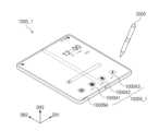
도 1을 참조하면, 전자 장치(1000)는 전기적 신호에 따라 활성화되는 장치일 수 있다. 예를 들어, 전자 장치(1000)는 휴대폰, 태블릿, 자동차 내비게이션, 게임기, 또는 웨어러블 장치일 수 있으나, 이에 제한되는 것은 아니다. 도 1에서는 전자 장치(1000)가 휴대폰인 것을 예시적으로 도시하였다.Referring to FIG. 1, the electronic device (1000) may be a device that is activated according to an electrical signal. For example, the electronic device (1000) may be, but is not limited to, a mobile phone, a tablet, a car navigation system, a game console, or a wearable device. In FIG. 1, the electronic device (1000) is illustrated as a mobile phone as an example.
전자 장치(1000)는 액티브 영역(1000A)을 통해 영상을 표시할 수 있다. 액티브 영역(1000A)은 제1 방향(DR1) 및 제2 방향(DR2)에 의해 정의된 면을 포함할 수 있다. 전자 장치(1000)의 두께 방향은 제1 방향(DR1) 및 제2 방향(DR2)과 교차하는 제3 방향(DR3)과 나란할 수 있다. 따라서, 전자 장치(1000)를 구성하는 부재들의 전면(또는 상면)과 배면(또는 하면)은 제3 방향(DR3)을 기준으로 정의될 수 있다.The electronic device (1000) can display an image through an active area (1000A). The active area (1000A) can include a surface defined by a first direction (DR1) and a second direction (DR2). A thickness direction of the electronic device (1000) can be parallel to a third direction (DR3) intersecting the first direction (DR1) and the second direction (DR2). Accordingly, the front (or upper surface) and the back (or lower surface) of the members constituting the electronic device (1000) can be defined based on the third direction (DR3).
전자 장치(1000)는 전자 장치(1000)의 외부에서 인가되는 입력들을 감지할 수 있다. 외부 입력은 사용자의 입력일 수 있다. 사용자의 입력은 사용자 신체의 일부, 액티브 펜(2000), 광, 열, 또는 압력 등 다양한 형태의 외부 입력들을 포함할 수 있다.The electronic device (1000) can detect inputs applied from outside the electronic device (1000). The external input may be a user's input. The user's input may include various forms of external inputs, such as a part of the user's body, an active pen (2000), light, heat, or pressure.
도 1에 도시된 전자 장치(1000)는 사용자의 터치에 의한 입력 및 액티브 펜(2000)에 의한 입력을 감지할 수 있다. 전자 장치(1000)와 액티브 펜(2000)은 양방향 통신이 가능할 수 있다. 전자 장치(1000)는 액티브 펜(2000)으로 업 링크 신호를 제공할 수 있다. 예를 들어, 업 링크 신호는 동기화 신호 또는 전자 장치(1000)의 정보를 포함할 수 있으나, 특별히 이에 제한되는 것은 아니다. 액티브 펜(2000)은 전자 장치(1000)로 다운 링크 신호를 제공할 수 있다. 다운 링크 신호는 동기화 신호 또는 액티브 펜(2000)의 상태 정보를 포함할 수 있다. 예를 들어, 다운 링크 신호는 액티브 펜의 좌표 정보, 액티브 펜의 배터리 정보, 액티브 펜의 기울기 정보, 및/또는 액티브 펜에 저장된 다양한 정보 등을 포함할 수 있으나, 특별히 이에 제한되는 것은 아니다.The electronic device (1000) illustrated in FIG. 1 can detect an input by a user's touch and an input by an active pen (2000). The electronic device (1000) and the active pen (2000) can be capable of bidirectional communication. The electronic device (1000) can provide an uplink signal to the active pen (2000). For example, the uplink signal may include a synchronization signal or information of the electronic device (1000), but is not particularly limited thereto. The active pen (2000) can provide a downlink signal to the electronic device (1000). The downlink signal may include a synchronization signal or status information of the active pen (2000). For example, the downlink signal may include coordinate information of the active pen, battery information of the active pen, tilt information of the active pen, and/or various information stored in the active pen, but is not particularly limited thereto.
도 2a 및 도 2b는 본 발명의 일 실시예에 따른 전자 장치의 사시도들이다.FIGS. 2A and 2B are perspective views of an electronic device according to one embodiment of the present invention.
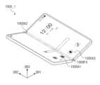
도 2a 및 도 2b를 참조하면, 전자 장치(1000_1)는 액티브 영역(1000A_1)을 통해 영상을 표시할 수 있다. 전자 장치(1000_1)가 언폴딩된 상태에서, 액티브 영역(1000A_1)은 제1 방향(DR1) 및 제2 방향(DR2)에 의해 정의된 평면을 포함할 수 있다.Referring to FIGS. 2A and 2B, the electronic device (1000_1) can display an image through the active area (1000A_1). When the electronic device (1000_1) is unfolded, the active area (1000A_1) can include a plane defined by a first direction (DR1) and a second direction (DR2).
액티브 영역(1000A_1)은 제1 영역(1000A1), 제2 영역(1000A2), 및 제3 영역(1000A3)을 포함할 수 있다. 제2 영역(1000A2)은 제2 방향(DR2)을 따라 연장하는 폴딩축(1000FX)을 기준으로 휘어질 수 있다. 따라서, 제1 영역(1000A1) 및 제3 영역(1000A3)은 비폴딩 영역들로 지칭될 수 있고, 제2 영역(1000A2)은 폴딩 영역으로 지칭될 수 있다.The active region (1000A_1) may include a first region (1000A1), a second region (1000A2), and a third region (1000A3). The second region (1000A2) may be bent about a folding axis (1000FX) extending along the second direction (DR2). Accordingly, the first region (1000A1) and the third region (1000A3) may be referred to as non-folding regions, and the second region (1000A2) may be referred to as a folding region.
전자 장치(1000_1)가 폴딩되면, 제1 영역(1000A1)과 제3 영역(1000A3)은 서로 마주할 수 있다. 따라서, 완전히 폴딩된 상태에서, 액티브 영역(1000A_1)은 외부로 노출되지 않을 수 있으며, 이는 인-폴딩(in-folding)으로 지칭될 수 있다. 다만, 이는 예시적인 것으로 전자 장치(1000_1)의 동작이 이에 제한되는 것은 아니다.When the electronic device (1000_1) is folded, the first region (1000A1) and the third region (1000A3) may face each other. Therefore, in a completely folded state, the active region (1000A_1) may not be exposed to the outside, which may be referred to as in-folding. However, this is an example and the operation of the electronic device (1000_1) is not limited thereto.
예를 들어, 본 발명의 일 실시예에서, 전자 장치(1000_1)가 폴딩되면, 제1 영역(1000A1)과 제3 영역(1000A3)은 서로 대향(opposing)할 수 있다. 따라서, 폴딩된 상태에서, 액티브 영역(1000A_1)은 외부로 노출될 수 있으며, 이는 아웃-폴딩(out-folding)으로 지칭될 수 있다.For example, in one embodiment of the present invention, when the electronic device (1000_1) is folded, the first region (1000A1) and the third region (1000A3) may be opposed to each other. Accordingly, in the folded state, the active region (1000A_1) may be exposed to the outside, which may be referred to as out-folding.
전자 장치(1000_1)는 인-폴딩 또는 아웃-폴딩 중 어느 하나의 동작만 가능할 수 있다. 또는 전자 장치(1000_1)는 인-폴딩 동작 및 아웃-폴딩 동작이 모두 가능할 수 있다. 이 경우, 전자 장치(1000_1)의 동일한 영역, 예를 들어, 제2 영역(1000A2)이 인-폴딩 및 아웃 폴딩될 수 있다.The electronic device (1000_1) may be capable of only one of the in-folding or out-folding operations. Alternatively, the electronic device (1000_1) may be capable of both the in-folding operation and the out-folding operation. In this case, the same region of the electronic device (1000_1), for example, the second region (1000A2), may be in-folded and out-folded.
도 2a 및 도 2b에서는 하나의 폴딩 영역과 두 개의 비폴딩 영역이 예를 들어 도시되었으나, 폴딩 영역과 비폴딩 영역의 개수가 이에 제한되는 것은 아니다. 예를 들어, 전자 장치(1000_1)는 2개보다 많은 복수 개의 비폴딩 영역들 및 서로 인접한 비폴딩 영역들 사이에 배치된 복수의 폴딩 영역들을 포함할 수 있다.In FIGS. 2A and 2B , one folding region and two non-folding regions are illustrated as examples, but the number of folding regions and non-folding regions is not limited thereto. For example, the electronic device (1000_1) may include a plurality of non-folding regions greater than two and a plurality of folding regions positioned between adjacent non-folding regions.
도 2a 및 도 2b에서는 폴딩축(1000FX)이 제2 방향(DR2)으로 연장된 것을 예시적으로 도시하였으나, 본 발명이 이에 제한되는 것은 아니다. 예를 들어, 폴딩축(1000FX)은 제1 방향(DR1)과 나란한 방향을 따라 연장할 수도 있다. 이 경우, 제1 영역(1000A1), 제2 영역(1000A2), 및 제3 영역(1000A3)은 제2 방향(DR2)을 따라 순차적으로 배열될 수 있다.In FIGS. 2A and 2B, the folding axis (1000FX) is exemplarily illustrated as extending in the second direction (DR2), but the present invention is not limited thereto. For example, the folding axis (1000FX) may extend along a direction parallel to the first direction (DR1). In this case, the first region (1000A1), the second region (1000A2), and the third region (1000A3) may be sequentially arranged along the second direction (DR2).
액티브 영역(1000A_1)은 적어도 하나의 전자 모듈들과 중첩될 수 있다. 예를 들어, 전자 모듈들은 카메라 모듈 및 근접 조도 센서 등을 포함할 수 있다. 전자 모듈들은 액티브 영역(1000A_1)을 통해 전달되는 외부 입력을 수신하거나, 액티브 영역(1000A_1)을 통해 출력을 제공할 수 있다. 카메라 모듈 및 근접 조도 센서 등과 중첩하는 액티브 영역(1000A_1)의 일부분은 액티브 영역(1000A_1)의 다른 일부분보다 높은 투과율을 가질 수 있다. 따라서, 복수의 전자 모듈들이 배치될 영역을 액티브 영역(1000A_1) 주변의 주변 영역(1000NA)에 제공하지 않아도 된다. 그 결과, 전자 장치(1000_1)의 전면 대비 액티브 영역(1000A_1)의 면적 비율은 증가될 수 있다.The active area (1000A_1) may overlap with at least one electronic module. For example, the electronic modules may include a camera module and a proximity light sensor, etc. The electronic modules may receive an external input transmitted through the active area (1000A_1) or provide an output through the active area (1000A_1). A portion of the active area (1000A_1) overlapping with the camera module and the proximity light sensor, etc. may have a higher transmittance than another portion of the active area (1000A_1). Accordingly, an area in which a plurality of electronic modules are arranged may not be provided in the peripheral area (1000NA) around the active area (1000A_1). As a result, the area ratio of the active area (1000A_1) to the front surface of the electronic device (1000_1) may increase.
전자 장치(1000_1)와 액티브 펜(2000)은 양방향 통신이 가능할 수 있다. 전자 장치(1000_1)는 액티브 펜(2000)으로 업 링크 신호를 제공할 수 있다. 액티브 펜(2000)은 전자 장치(1000_1)로 다운 링크 신호를 제공할 수 있다. 전자 장치(1000_1)는 액티브 펜(2000)으로부터 제공되는 신호를 이용하여 액티브 펜(2000)의 좌표를 감지할 수 있다.The electronic device (1000_1) and the active pen (2000) may be capable of bidirectional communication. The electronic device (1000_1) may provide an uplink signal to the active pen (2000). The active pen (2000) may provide a downlink signal to the electronic device (1000_1). The electronic device (1000_1) may detect the coordinates of the active pen (2000) using the signal provided from the active pen (2000).
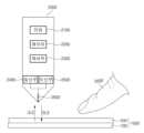
도 3은 본 발명의 일 실시예에 따른 전자 장치와 액티브 펜을 개략적으로 도시한 블록도이다.FIG. 3 is a block diagram schematically illustrating an electronic device and an active pen according to one embodiment of the present invention.
도 3을 참조하면, 전자 장치(1000)는 표시층(100) 및 센서층(200)을 포함할 수 있다.Referring to FIG. 3, the electronic device (1000) may include a display layer (100) and a sensor layer (200).
표시층(100)은 영상을 실질적으로 생성하는 구성일 수 있다. 표시층(100)은 발광형 표시층일 수 있으며, 예를 들어, 표시층(100)은 유기발광 표시층, 퀀텀닷 표시층, 마이크로 엘이디 표시층, 또는 나노 엘이디 표시층일 수 있다.The display layer (100) may be a configuration that actually generates an image. The display layer (100) may be a light-emitting display layer, and for example, the display layer (100) may be an organic light-emitting display layer, a quantum dot display layer, a micro LED display layer, or a nano LED display layer.
센서층(200)은 표시층(100) 위에 배치될 수 있다. 센서층(200)은 외부에서 인가되는 외부 입력을 감지할 수 있다. 센서층(200)은 사용자 신체(3000)에 의한 입력 및 액티브 펜(2000)에 의한 입력을 모두 센싱할 수 있다.The sensor layer (200) can be placed on the display layer (100). The sensor layer (200) can detect external input applied from the outside. The sensor layer (200) can sense both input by the user's body (3000) and input by the active pen (2000).
센서층(200)은 시분할 구동되어 동작될 수 있다. 예를 들어, 센서층(200)은 제1 모드 및 제2 모드로 교대로 반복되어 구동될 수 있다. 상기 제1 모드는 사용자 신체(3000)에 의한 입력을 감지하는 모드일 수 있고, 상기 제2 모드는 액티브 펜(2000)에 의한 입력을 감지하는 모드일 수 있다.The sensor layer (200) may be operated in a time-division manner. For example, the sensor layer (200) may be operated alternately and repeatedly in a first mode and a second mode. The first mode may be a mode for detecting input by a user's body (3000), and the second mode may be a mode for detecting input by an active pen (2000).
상기 제2 모드가 시작될 때, 센서층(200)은 액티브 펜(2000)으로 업링크 신호(ULS)를 제공할 수 있다. 액티브 펜(2000)이 업링크 신호(ULS)를 수신하여 전자 장치(1000)와 동기화되는 경우, 액티브 펜(2000)은 센서층(200)을 향해 다운 링크 신호(DLS)를 제공할 수 있다.When the second mode is started, the sensor layer (200) can provide an uplink signal (ULS) to the active pen (2000). When the active pen (2000) receives the uplink signal (ULS) and is synchronized with the electronic device (1000), the active pen (2000) can provide a downlink signal (DLS) toward the sensor layer (200).
액티브 펜(2000)은 전원(2100), 메모리(2200), 제어부(2300), 송신부(2400), 수신부(2500), 및 펜 팁(2600)을 포함할 수 있다. 다만, 액티브 펜(2000)을 구성하는 구성 요소들이 상기 나열된 구성 요소들에 제한되는 것은 아니다. 예를 들어, 액티브 펜(2000)은 펜 팁(2600)을 신호 송신 모드 또는 신호 수신 모드로 전환하는 전극 스위치, 압력을 감지하는 압력 센서, 또는 회전을 감지하는 회전 센서 등을 더 포함할 수도 있다.The active pen (2000) may include a power supply (2100), a memory (2200), a control unit (2300), a transmitter (2400), a receiver (2500), and a pen tip (2600). However, the components constituting the active pen (2000) are not limited to the components listed above. For example, the active pen (2000) may further include an electrode switch that switches the pen tip (2600) to a signal transmission mode or a signal reception mode, a pressure sensor that detects pressure, or a rotation sensor that detects rotation.
전원(2100)은 액티브 펜(2000)에 전원을 공급하는 배터리를 포함할 수 있다. 메모리(2200)는 액티브 펜(2000)의 기능 정보를 저장할 수 있다. 제어부(2300)는 액티브 펜(2000)의 동작을 제어할 수 있다. 송신부(2400) 및 수신부(2500) 각각은 펜 팁(2600)을 통해 전자 장치(1000)와 통신할 수 있다. 송신부(2400)는 신호 발생기 또는 송신 회로로 지칭될 수 있고, 수신부(2500)는 신호 수신기 또는 수신 회로로 지칭될 수 있다.The power supply (2100) may include a battery that supplies power to the active pen (2000). The memory (2200) may store function information of the active pen (2000). The control unit (2300) may control the operation of the active pen (2000). Each of the transmitter (2400) and the receiver (2500) may communicate with the electronic device (1000) through the pen tip (2600). The transmitter (2400) may be referred to as a signal generator or a transmitter circuit, and the receiver (2500) may be referred to as a signal receiver or a receiver circuit.
도 4는 본 발명의 일 실시예에 따른 전자 장치의 단면도이다.FIG. 4 is a cross-sectional view of an electronic device according to one embodiment of the present invention.
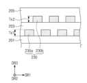
도 4를 참조하면, 표시층(100)은 베이스층(110), 회로층(120), 발광 소자층(130), 및 봉지층(140)을 포함할 수 있다.Referring to FIG. 4, the display layer (100) may include a base layer (110), a circuit layer (120), a light-emitting element layer (130), and an encapsulation layer (140).
베이스층(110)은 회로층(120)이 배치되는 베이스 면을 제공하는 부재일 수 있다. 베이스층(110)은 유리기판, 금속기판, 또는 고분자 기판 등일 수 있다. 하지만, 실시예가 이에 한정되는 것은 아니며, 베이스층(110)은 무기층, 유기층 또는 복합재료층일 수 있다.The base layer (110) may be a member that provides a base surface on which the circuit layer (120) is arranged. The base layer (110) may be a glass substrate, a metal substrate, a polymer substrate, or the like. However, the embodiment is not limited thereto, and the base layer (110) may be an inorganic layer, an organic layer, or a composite material layer.
베이스층(110)은 다층 구조를 가질 수 있다. 예를 들어, 베이스층(110)은 합성수지층, 접착층, 및 합성수지층의 3층 구조를 가질 수도 있다. 특히, 합성수지층은 폴리이미드(polyimide)계 수지를 포함하는 것일 수 있다. 또한, 합성수지층은 아크릴(acrylate)계 수지, 메타크릴(methacrylate)계 수지, 폴리아이소프렌(polyisoprene)계 수지, 비닐(vinyl)계 수지, 에폭시(epoxy)계 수지, 우레탄(urethane)계 수지, 셀룰로오스(cellulose)계 수지, 실록산(siloxane)계 수지, 폴리아미드(polyamide)계 수지 및 페릴렌(perylene)계 수지 중 적어도 하나를 포함하는 것일 수 있다. 한편, 본 명세서에서 "~~" 계 수지는 "~~" 의 작용기를 포함하는 것을 의미한다.The base layer (110) may have a multilayer structure. For example, the base layer (110) may have a three-layer structure of a synthetic resin layer, an adhesive layer, and a synthetic resin layer. In particular, the synthetic resin layer may include a polyimide-based resin. In addition, the synthetic resin layer may include at least one of an acrylate-based resin, a methacrylate-based resin, a polyisoprene-based resin, a vinyl-based resin, an epoxy-based resin, a urethane-based resin, a cellulose-based resin, a siloxane-based resin, a polyamide-based resin, and a perylene-based resin. Meanwhile, in the present specification, the “~~”-based resin means one that includes a functional group of “~~”.
회로층(120)은 베이스층(110) 위에 배치될 수 있다. 회로층(120)은 절연층, 반도체 패턴, 도전 패턴, 및 신호 라인 등을 포함할 수 있다. 코팅, 증착 등의 방식으로 절연층, 반도체층, 및 도전층이 베이스층(110) 위에 형성되고, 이후, 복수 회의 포토리소그래피 공정을 통해 절연층, 반도체층, 및 도전층이 선택적으로 패터닝될 수 있다. 이 후, 회로층(120)에 포함된 반도체 패턴, 도전 패턴, 및 신호 라인이 형성될 수 있다.The circuit layer (120) may be arranged on the base layer (110). The circuit layer (120) may include an insulating layer, a semiconductor pattern, a conductive pattern, and a signal line. The insulating layer, the semiconductor layer, and the conductive layer are formed on the base layer (110) by a coating, deposition, or the like, and then the insulating layer, the semiconductor layer, and the conductive layer may be selectively patterned through a plurality of photolithography processes. Thereafter, the semiconductor pattern, the conductive pattern, and the signal line included in the circuit layer (120) may be formed.
베이스층(110)의 상면에 적어도 하나의 무기층이 형성된다. 무기층은 알루미늄옥사이드, 티타늄옥사이드, 실리콘옥사이드 실리콘옥시나이트라이드, 지르코늄옥사이드, 및 하프늄옥사이드 중 적어도 하나를 포함할 수 있다. 무기층은 다층으로 형성될 수 있다. 다층의 무기층들은 배리어층 및/또는 버퍼층을 구성할 수 있다. 본 실시예에서 표시층(100)은 버퍼층(BFL)을 포함하는 것으로 도시되었다.At least one inorganic layer is formed on the upper surface of the base layer (110). The inorganic layer may include at least one of aluminum oxide, titanium oxide, silicon oxide, silicon oxynitride, zirconium oxide, and hafnium oxide. The inorganic layer may be formed in multiple layers. The multiple inorganic layers may constitute a barrier layer and/or a buffer layer. In the present embodiment, the display layer (100) is illustrated as including a buffer layer (BFL).
버퍼층(BFL)은 베이스층(110)과 반도체 패턴 사이의 결합력을 향상시킬 수 있다. 버퍼층(BFL)은 실리콘옥사이드층 및 실리콘나이트라이드층을 포함할 수 있으며, 실리콘옥사이드층과 실리콘나이트라이드층은 교대로 적층될 수 있다.The buffer layer (BFL) can improve the bonding strength between the base layer (110) and the semiconductor pattern. The buffer layer (BFL) can include a silicon oxide layer and a silicon nitride layer, and the silicon oxide layer and the silicon nitride layer can be alternately laminated.
반도체 패턴은 버퍼층(BFL) 위에 배치될 수 있다. 반도체 패턴은 폴리실리콘을 포함할 수 있다. 그러나 이에 제한되지 않고, 반도체 패턴은 비정질실리콘 또는 금속 산화물을 포함할 수도 있다.The semiconductor pattern may be disposed on a buffer layer (BFL). The semiconductor pattern may include polysilicon. However, without limitation, the semiconductor pattern may also include amorphous silicon or a metal oxide.
도 4은 일부의 반도체 패턴을 도시한 것일 뿐이고, 다른 영역에 반도체 패턴이 더 배치될 수 있다. 반도체 패턴은 화소들에 걸쳐 특정한 규칙으로 배열될 수 있다. 반도체 패턴은 도핑 여부에 따라 전기적 성질이 다를 수 있다. 반도체 패턴은 도핑영역과 비-도핑영역을 포함할 수 있다. 도핑영역은 N형 도판트 또는 P형 도판트로 도핑될 수 있다. P타입의 트랜지스터는 P형 도판트로 도핑된 도핑영역을 포함하고, N타입의 트랜지스터는 N형 도판트로 도핑된 도핑영역을 포함할 수 있다.FIG. 4 only illustrates some semiconductor patterns, and semiconductor patterns may be further arranged in other areas. The semiconductor patterns may be arranged in a specific rule across the pixels. The semiconductor patterns may have different electrical properties depending on whether they are doped. The semiconductor patterns may include doped regions and non-doped regions. The doped region may be doped with an N-type dopant or a P-type dopant. A P-type transistor may include a doped region doped with a P-type dopant, and an N-type transistor may include a doped region doped with an N-type dopant.
도핑영역은 비-도핑영역보다 전도성이 크고, 실질적으로 전극 또는 신호 라인의 역할을 할 수 있다. 비-도핑영역은 실질적으로 트랜지스터의 액티브(또는 채널)에 해당할 수 있다. 다시 말해, 반도체 패턴의 일부분은 트랜지스터의 액티브일수 있고, 다른 일부분은 트랜지스터의 소스 또는 드레인일 수 있고, 또 다른 일부분은 연결 전극 또는 연결 신호라인일 수 있다.The doped region is more conductive than the non-doped region and can actually function as an electrode or a signal line. The non-doped region can actually correspond to the active (or channel) of the transistor. In other words, a part of the semiconductor pattern can be the active part of the transistor, another part can be the source or drain of the transistor, and another part can be a connecting electrode or a connecting signal line.
화소들 각각은 7개의 트랜지스터들, 하나의 커패시터, 및 발광 소자를 포함하는 등가회로를 가질 수 있으며, 화소의 등가회로도는 다양한 형태로 변형될 수 있다. 도 4에서는 화소에 포함되는 하나의 트랜지스터(100PC) 및 발광 소자(100PE)를 예시적으로 도시하였다.Each of the pixels can have an equivalent circuit including seven transistors, one capacitor, and a light-emitting element, and the equivalent circuit diagram of the pixel can be modified in various forms. FIG. 4 illustrates one transistor (100PC) and a light-emitting element (100PE) included in the pixel as an example.
트랜지스터(100PC)의 소스(SC1), 액티브(A1), 및 드레인(D1)이 반도체 패턴으로부터 형성될 수 있다. 소스(SC1) 및 드레인(D1)은 단면 상에서 액티브(A1)로부터 서로 반대 방향으로 연장될 수 있다. 도 4에는 반도체 패턴으로부터 형성된 연결 신호 라인(SCL)의 일부분을 도시하였다. 별도로 도시하지 않았으나, 연결 신호 라인(SCL)은 평면 상에서 트랜지스터(100PC)의 드레인(D1)에 전기적으로 연결될 수 있다.The source (SC1), the active (A1), and the drain (D1) of the transistor (100PC) can be formed from a semiconductor pattern. The source (SC1) and the drain (D1) can extend in opposite directions from the active (A1) in a cross-section. Fig. 4 illustrates a part of a connection signal line (SCL) formed from the semiconductor pattern. Although not illustrated separately, the connection signal line (SCL) can be electrically connected to the drain (D1) of the transistor (100PC) in a plane.
제1 절연층(10)은 버퍼층(BFL) 위에 배치될 수 있다. 제1 절연층(10)은 복수 개의 화소들에 공통으로 중첩하며, 반도체 패턴을 커버할 수 있다. 제1 절연층(10)은 무기층 및/또는 유기층일 수 있으며, 단층 또는 다층 구조를 가질 수 있다. 제1 절연층(10)은 알루미늄옥사이드, 티타늄옥사이드, 실리콘옥사이드, 실리콘옥시나이트라이드, 지르코늄옥사이드, 및 하프늄옥사이드 중 적어도 하나를 포함할 수 있다. 본 실시예에서 제1 절연층(10)은 단층의 실리콘옥사이드층일 수 있다. 제1 절연층(10)뿐만 아니라 후술하는 회로층(120)의 절연층은 무기층 및/또는 유기층일 있으며, 단층 또는 다층 구조를 가질 수 있다. 무기층은 상술한 물질 중 적어도 하나를 포함할 수 있으나, 이에 제한되는 것은 아니다.The first insulating layer (10) may be disposed on a buffer layer (BFL). The first insulating layer (10) may overlap a plurality of pixels in common and cover a semiconductor pattern. The first insulating layer (10) may be an inorganic layer and/or an organic layer, and may have a single-layer or multi-layer structure. The first insulating layer (10) may include at least one of aluminum oxide, titanium oxide, silicon oxide, silicon oxynitride, zirconium oxide, and hafnium oxide. In the present embodiment, the first insulating layer (10) may be a single-layer silicon oxide layer. Not only the first insulating layer (10), but also the insulating layer of the circuit layer (120) described below may be an inorganic layer and/or an organic layer, and may have a single-layer or multi-layer structure. The inorganic layer may include at least one of the materials described above, but is not limited thereto.
트랜지스터(100PC)의 게이트(G1)는 제1 절연층(10) 위에 배치된다. 게이트(G1)는 금속 패턴의 일부분일 수 있다. 게이트(G1)는 액티브(A1)에 중첩한다. 반도체 패턴을 도핑하는 공정에서 게이트(G1)는 마스크로 기능할 수 있다.The gate (G1) of the transistor (100PC) is placed on the first insulating layer (10). The gate (G1) may be a part of a metal pattern. The gate (G1) overlaps the active (A1). In the process of doping the semiconductor pattern, the gate (G1) may function as a mask.
제2 절연층(20)은 제1 절연층(10) 위에 배치되며, 게이트(G1)를 커버할 수 있다. 제2 절연층(20)은 화소들에 공통으로 중첩할 수 있다. 제2 절연층(20)은 무기층 및/또는 유기층일 수 있으며, 단층 또는 다층 구조를 가질 수 있다. 본 실시예에서 제2 절연층(20)은 단층의 실리콘옥사이드층일 수 있다.The second insulating layer (20) is arranged on the first insulating layer (10) and can cover the gate (G1). The second insulating layer (20) can be commonly overlapped with the pixels. The second insulating layer (20) can be an inorganic layer and/or an organic layer and can have a single-layer or multi-layer structure. In the present embodiment, the second insulating layer (20) can be a single-layer silicon oxide layer.
제3 절연층(30)은 제2 절연층(20) 위에 배치될 수 있으며, 본 실시예에서 제3 절연층(30)은 단층의 실리콘옥사이드층일 수 있다.The third insulating layer (30) may be placed on the second insulating layer (20), and in this embodiment, the third insulating layer (30) may be a single-layer silicon oxide layer.
제1 연결 전극(CNE1)은 제3 절연층(30) 위에 배치될 수 있다. 제1 연결 전극(CNE1)은 제1, 제2, 및 제3 절연층(10, 20, 30)을 관통하는 컨택홀(CNT-1)을 통해 연결 신호 라인(SCL)에 접속될 수 있다.The first connection electrode (CNE1) may be placed on the third insulating layer (30). The first connection electrode (CNE1) may be connected to the connection signal line (SCL) through a contact hole (CNT-1) penetrating the first, second, and third insulating layers (10, 20, 30).
제4 절연층(40)은 제3 절연층(30) 위에 배치될 수 있다. 제4 절연층(40)은 단층의 실리콘 옥사이드층일 수 있다. 제5 절연층(50)은 제4 절연층(40) 위에 배치될 수 있다. 제5 절연층(50)은 유기층일 수 있다.The fourth insulating layer (40) may be disposed on the third insulating layer (30). The fourth insulating layer (40) may be a single-layer silicon oxide layer. The fifth insulating layer (50) may be disposed on the fourth insulating layer (40). The fifth insulating layer (50) may be an organic layer.
제2 연결 전극(CNE2)은 제5 절연층(50) 위에 배치될 수 있다. 제2 연결 전극(CNE2)은 제4 절연층(40) 및 제5 절연층(50)을 관통하는 컨택홀(CNT-2)을 통해 제1 연결 전극(CNE1)에 접속될 수 있다.The second connecting electrode (CNE2) may be placed on the fifth insulating layer (50). The second connecting electrode (CNE2) may be connected to the first connecting electrode (CNE1) through a contact hole (CNT-2) penetrating the fourth insulating layer (40) and the fifth insulating layer (50).
제6 절연층(60)은 제5 절연층(50) 위에 배치되며, 제2 연결 전극(CNE2)을 커버할 수 있다. 제6 절연층(60)은 유기층일 수 있다. 발광 소자층(130)은 회로층(120) 위에 배치될 수 있다. 발광 소자층(130)은 발광 소자를 포함할 수 있다. 예를 들어, 발광 소자층(130)은 유기 발광 물질, 퀀텀닷, 퀀텀 로드, 마이크로 엘이디, 또는 나노 엘이디를 포함할 수 있다. 발광 소자(100PE)는 제1 전극(AE), 발광층(EL), 및 제2 전극(CE)을 포함할 수 있다.The sixth insulating layer (60) is disposed on the fifth insulating layer (50) and can cover the second connection electrode (CNE2). The sixth insulating layer (60) can be an organic layer. The light-emitting element layer (130) can be disposed on the circuit layer (120). The light-emitting element layer (130) can include a light-emitting element. For example, the light-emitting element layer (130) can include an organic light-emitting material, a quantum dot, a quantum rod, a micro LED, or a nano LED. The light-emitting element (100PE) can include a first electrode (AE), an emission layer (EL), and a second electrode (CE).
제1 전극(AE)은 제6 절연층(60) 위에 배치될 수 있다. 제1 전극(AE)은 제6 절연층(60)을 관통하는 컨택홀(CNT-3)을 통해 제2 연결 전극(CNE2)에 연결될 수 있다.The first electrode (AE) may be placed on the sixth insulating layer (60). The first electrode (AE) may be connected to the second connection electrode (CNE2) through a contact hole (CNT-3) penetrating the sixth insulating layer (60).
화소 정의막(70)은 제6 절연층(60) 위에 배치되며, 제1 전극(AE)의 일부분을 커버할 수 있다. 화소 정의막(70)에는 개구부(70-OP)가 정의된다. 화소 정의막(70)의 개구부(70-OP)는 제1 전극(AE)의 적어도 일부분을 노출시킨다. 본 실시예에서 발광 영역(PXA)은 개구부(70-OP)에 의해 노출된 제1 전극(AE)의 일부 영역에 대응하게 정의되었다. 비발광 영역(NPXA)은 발광 영역(PXA)을 에워쌀 수 있다.The pixel defining film (70) is disposed on the sixth insulating layer (60) and can cover a portion of the first electrode (AE). An opening (70-OP) is defined in the pixel defining film (70). The opening (70-OP) of the pixel defining film (70) exposes at least a portion of the first electrode (AE). In the present embodiment, the light-emitting area (PXA) is defined to correspond to a portion of the first electrode (AE) exposed by the opening (70-OP). The non-light-emitting area (NPXA) can surround the light-emitting area (PXA).
발광층(EL)은 제1 전극(AE) 위에 배치될 수 있다. 발광층(EL)은 개구부(70-OP)에 배치될 수 있다. 즉, 발광층(EL)은 화소들 각각에 분리되어 형성될 수 있다. 발광층(EL)이 화소들 각각에 분리되어 형성된 경우, 발광층들(EL) 각각은 청색, 적색, 및 녹색 중 적어도 하나의 색의 광을 발광할 수 있다. 다만, 이에 제한되는 것은 아니며, 발광층(EL)은 화소들에 연결되어 공통으로 제공될 수도 있다. 이 경우, 발광층(EL)은 청색 광을 제공하거나, 백색 광을 제공할 수도 있다.The light-emitting layer (EL) may be disposed on the first electrode (AE). The light-emitting layer (EL) may be disposed in the opening (70-OP). That is, the light-emitting layer (EL) may be formed separately for each pixel. When the light-emitting layer (EL) is formed separately for each pixel, each of the light-emitting layers (EL) may emit light of at least one color among blue, red, and green. However, the present invention is not limited thereto, and the light-emitting layer (EL) may be connected to the pixels and provided in common. In this case, the light-emitting layer (EL) may provide blue light or white light.
제2 전극(CE)은 발광층(EL) 위에 배치될 수 있다. 제2 전극(CE)은 일체의 형상을 갖고, 복수 개의 화소들에 공통적으로 배치될 수 있다. 제2 전극(CE)에는 공통 전압이 제공될 수 있으며, 제2 전극(CE)은 공통 전극으로 지칭될 수 있다.The second electrode (CE) may be arranged on the light-emitting layer (EL). The second electrode (CE) may have an integral shape and may be arranged commonly across a plurality of pixels. A common voltage may be provided to the second electrode (CE), and the second electrode (CE) may be referred to as a common electrode.
도시되지 않았으나, 제1 전극(AE)과 발광층(EL) 사이에는 정공 제어층이 배치될 수 있다. 정공 제어층은 발광 영역(PXA)과 비발광 영역(NPXA)에 공통으로 배치될 수 있다. 정공 제어층은 정공 수송층을 포함하고, 정공 주입층을 더 포함할 수 있다. 발광층(EL)과 제2 전극(CE) 사이에는 전자 제어층이 배치될 수 있다. 전자 제어층은 전자 수송층을 포함하고, 전자 주입층을 더 포함할 수 있다. 정공 제어층과 전자 제어층은 오픈 마스크를 이용하여 복수 개의 화소들에 공통으로 형성될 수 있다. 봉지층(140)은 발광 소자층(130) 위에 배치될 수 있다. 봉지층(140)은 순차적으로 적층된 무기층, 유기층, 및 무기층을 포함할 수 있으나, 봉지층(140)을 구성하는 층들이 이에 제한되는 것은 아니다.Although not shown, a hole control layer may be arranged between the first electrode (AE) and the light emitting layer (EL). The hole control layer may be arranged commonly in the light emitting area (PXA) and the non-light emitting area (NPXA). The hole control layer may include a hole transport layer and may further include a hole injection layer. An electron control layer may be arranged between the light emitting layer (EL) and the second electrode (CE). The electron control layer may include an electron transport layer and may further include an electron injection layer. The hole control layer and the electron control layer may be commonly formed for a plurality of pixels using an open mask. The encapsulation layer (140) may be arranged on the light emitting element layer (130). The encapsulation layer (140) may include an inorganic layer, an organic layer, and an inorganic layer that are sequentially laminated, but the layers constituting the encapsulation layer (140) are not limited thereto.
무기층들은 수분 및 산소로부터 발광 소자층(130)을 보호하고, 유기층은 먼지 입자와 같은 이물질로부터 발광 소자층(130)을 보호할 수 있다. 무기층들은 실리콘나이트라이드층, 실리콘옥시나이트라이드층, 실리콘옥사이드층, 티타늄옥사이드층, 또는 알루미늄옥사이드층 등을 포함할 수 있다. 유기층은 아크릴 계열 유기층을 포함할 수 있고, 이에 제한되지 않는다.The inorganic layers can protect the light emitting element layer (130) from moisture and oxygen, and the organic layers can protect the light emitting element layer (130) from foreign substances such as dust particles. The inorganic layers can include a silicon nitride layer, a silicon oxynitride layer, a silicon oxide layer, a titanium oxide layer, or an aluminum oxide layer. The organic layer can include an acrylic-based organic layer, but is not limited thereto.
센서층(200)은 연속된 공정을 통해 표시층(100) 위에 형성될 수 있다. 이 경우, 센서층(200)은 표시층(100) 위에 직접 배치된다고 표현될 수 있다. 직접 배치된다는 것은 센서층(200)과 표시층(100) 사이에 제3 의 구성요소가 배치되지 않는 것을 의미할 수 있다. 즉, 센서층(200)과 표시층(100) 사이에는 별도의 접착 부재가 배치되지 않을 수 있다. 이 경우, 전자 장치(1000)의 두께는 더 얇아질 수 있다. 또한, 표시층(100)과 센서층(200)의 두께가 얇아질수록 유연성이 향상되기 때문에, 폴더블 전자 장치(1000_1, 도 2a 참조)에 적용될 수 있다.The sensor layer (200) may be formed on the display layer (100) through a continuous process. In this case, the sensor layer (200) may be expressed as being directly disposed on the display layer (100). Being directly disposed may mean that a third component is not disposed between the sensor layer (200) and the display layer (100). In other words, a separate adhesive material may not be disposed between the sensor layer (200) and the display layer (100). In this case, the thickness of the electronic device (1000) may be thinner. In addition, since the flexibility is improved as the thickness of the display layer (100) and the sensor layer (200) becomes thinner, it may be applied to a foldable electronic device (1000_1, see FIG. 2a).
센서층(200)은 베이스층(201), 제1 도전층(202), 감지 절연층(203), 제2 도전층(204), 및 커버 절연층(205)을 포함할 수 있다.The sensor layer (200) may include a base layer (201), a first conductive layer (202), a detection insulating layer (203), a second conductive layer (204), and a cover insulating layer (205).
베이스층(201)은 실리콘나이트라이드, 실리콘옥시나이트라이드, 및 실리콘옥사이드 중 어느 하나를 포함하는 무기층일 수 있다. 또는 베이스층(201)은 에폭시 수지, 아크릴 수지, 또는 이미드 계열 수지를 포함하는 유기층일 수도 있다. 베이스층(201)은 단층 구조를 갖거나, 제3 방향(DR3)을 따라 적층된 다층 구조를 가질 수 있다.The base layer (201) may be an inorganic layer including one of silicon nitride, silicon oxynitride, and silicon oxide. Alternatively, the base layer (201) may be an organic layer including an epoxy resin, an acrylic resin, or an imide-based resin. The base layer (201) may have a single-layer structure or a multi-layer structure laminated along the third direction (DR3).
제1 도전층(202) 및 제2 도전층(204) 각각은 단층구조를 갖거나, 제3 방향(DR3)을 따라 적층된 다층 구조를 가질 수 있다.Each of the first conductive layer (202) and the second conductive layer (204) may have a single-layer structure or a multi-layer structure laminated along the third direction (DR3).
단층구조의 도전층은 금속층 또는 투명 도전층을 포함할 수 있다. 금속층은 몰리브덴, 은, 티타늄, 구리, 알루미늄, 또는 이들의 합금을 포함할 수 있다. 투명 도전층은 인듐주석산화물(indium tin oxide, ITO), 인듐아연산화물(indium zinc oxide, IZO), 산화아연(zinc oxide, ZnO), 인듐아연주석산화물(indium zinc tin oxide, IZTO) 등과 같은 투명한 전도성산화물을 포함할 수 있다. 그밖에 투명 도전층은 PEDOT과 같은 전도성 고분자, 금속 나노 와이어, 그라핀 등을 포함할 수 있다.The conductive layer of the single-layer structure may include a metal layer or a transparent conductive layer. The metal layer may include molybdenum, silver, titanium, copper, aluminum, or an alloy thereof. The transparent conductive layer may include a transparent conductive oxide such as indium tin oxide (ITO), indium zinc oxide (IZO), zinc oxide (ZnO), or indium zinc tin oxide (IZTO). In addition, the transparent conductive layer may include a conductive polymer such as PEDOT, metal nanowires, graphene, or the like.
다층구조의 도전층은 금속층들을 포함할 수 있다. 금속층들은 예컨대 티타늄/알루미늄/티타늄의 3층 구조를 가질 수 있다. 다층구조의 도전층은 적어도 하나의 금속층 및 적어도 하나의 투명 도전층을 포함할 수 있다.The multilayer conductive layer may include metal layers. The metal layers may have a three-layer structure of, for example, titanium/aluminum/titanium. The multilayer conductive layer may include at least one metal layer and at least one transparent conductive layer.
감지 절연층(203) 및 커버 절연층(205) 중 적어도 어느 하나는 무기막을 포함할 수 있다. 무기막은 알루미늄옥사이드, 티타늄옥사이드, 실리콘옥사이드, 실리콘옥시나이트라이드, 지르코늄옥사이드, 및 하프늄옥사이드 중 적어도 하나를 포함할 수 있다.At least one of the sensing insulating layer (203) and the cover insulating layer (205) may include an inorganic film. The inorganic film may include at least one of aluminum oxide, titanium oxide, silicon oxide, silicon oxynitride, zirconium oxide, and hafnium oxide.
감지 절연층(203) 및 커버 절연층(205) 중 적어도 어느 하나는 유기막을 포함할 수 있다. 유기막은 아크릴계 수지, 메타크릴계 수지, 폴리이소프렌, 비닐계 수지, 에폭시계 수지, 우레탄계 수지, 셀룰로오스계 수지, 실록산계 수지, 폴리이미드계 수지, 폴리아미드계 수지 및 페릴렌계 수지 중 적어도 어느 하나를 포함할 수 있다.At least one of the sensing insulating layer (203) and the cover insulating layer (205) may include an organic film. The organic film may include at least one of an acrylic resin, a methacrylic resin, a polyisoprene, a vinyl resin, an epoxy resin, a urethane resin, a cellulose resin, a siloxane resin, a polyimide resin, a polyamide resin, and a perylene resin.
센서층(200)과 제2 전극(CE) 사이에는 기생 정전용량(Cb)이 발생될 수 있다. 기생 정전용량(Cb)은 베이스 정전용량으로 지칭될 수도 있다. 센서층(200)과 제2 전극(CE)의 거리가 가까워짐에 따라 기생 정전용량(Cb) 값은 증가될 수 있다. 기생 정전용량(Cb)이 커지면 커질수록 기준 값 대비 정전 용량의 변화량의 비율이 작아질 수 있다. 정전 용량의 변화량은 입력 수단, 예를 들어, 액티브 펜(2000, 도 3 참조) 또는 사용자 신체(3000, 도 3 참조), 에 의한 입력 전과 입력 후 사이에 발생하는 정전 용량의 변화를 의미한다.A parasitic capacitance (Cb) may be generated between the sensor layer (200) and the second electrode (CE). The parasitic capacitance (Cb) may also be referred to as base capacitance. As the distance between the sensor layer (200) and the second electrode (CE) becomes closer, the parasitic capacitance (Cb) value may increase. As the parasitic capacitance (Cb) increases, the ratio of the change in capacitance to the reference value may decrease. The change in capacitance refers to a change in capacitance that occurs between before and after an input by an input means, for example, an active pen (2000, see FIG. 3) or a user's body (3000, see FIG. 3).
센서층(200)으로부터 감지된 신호를 처리하는 구동칩은 감지된 신호에서 기생 정전용량(Cb)에 대응하는 값을 제거하는 레벨링 동작을 수행할 수 있다. 상기 레벨링 동작에 의해 기준 값 대비 정전 용량의 변화량의 비율은 증가되어 센싱 감도가 향상될 수 있다.The driving chip that processes the signal detected from the sensor layer (200) can perform a leveling operation that removes a value corresponding to the parasitic capacitance (Cb) from the detected signal. By the leveling operation, the ratio of the change in the capacitance compared to the reference value increases, so that the sensing sensitivity can be improved.
하지만, 구동칩의 스펙에 따라 기생 정전용량(Cb)에 대응하는 값을 제거하는 능력에 차이가 있을 수 있다. 예를 들어, 최대 기생 정전용량(Cb)이 500피코패럿이고, 상기 구동칩이 센서층(200)으로부터 감지된 신호로부터 제거할 수 있는 정전용량 값이 200피코패럿이라면, 상기 구동칩에 의해 기준 값은 충분히 낮아지지 않을 수 있다. 이 경우, 기준 값에 비해 정전 용량의 변화량의 비율은 미미하여, 상기 구동칩이 정전 용량의 변화량을 노이즈로 인식하거나, 인식하지 못하여 터치 좌표를 감지하지 못하는 오동작이 발생될 수 있다. 본 발명의 실시예에 따르면, 센서층(200)의 전극 구조를 변형하여, 기생 정전용량(Cb)의 최대 값을 소정 값 이하로 제공할 수 있다. 이 경우, 상기 구동칩의 성능이 비교적 낮은 경우에도 좌표 인식 정확도가 향상될 수 있다. 상기 소정 값은 200 피코패럿일 수 있으나, 특별히 이에 제한되는 것은 아니다.However, depending on the specifications of the driving chip, there may be differences in the ability to remove a value corresponding to the parasitic capacitance (Cb). For example, if the maximum parasitic capacitance (Cb) is 500 picofarads and the capacitance value that the driving chip can remove from the signal detected from the sensor layer (200) is 200 picofarads, the reference value may not be sufficiently lowered by the driving chip. In this case, the ratio of the amount of change in the capacitance compared to the reference value is minimal, so that the driving chip may recognize the amount of change in the capacitance as noise or may not recognize it, resulting in a malfunction in which the touch coordinates are not detected. According to an embodiment of the present invention, by modifying the electrode structure of the sensor layer (200), the maximum value of the parasitic capacitance (Cb) can be provided below a predetermined value. In this case, even when the performance of the driving chip is relatively low, the accuracy of coordinate recognition can be improved. The predetermined value may be 200 picofarads, but is not particularly limited thereto.
도 5는 본 발명의 일 실시예에 따른 센서층을 도시한 평면도이다.FIG. 5 is a plan view illustrating a sensor layer according to one embodiment of the present invention.
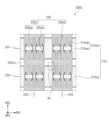
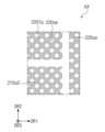
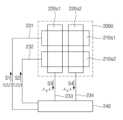
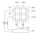
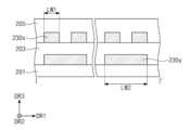
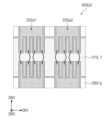
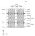
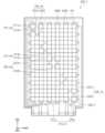
도 5를 참조하면, 센서층(200)은 감지 영역(200A) 및 주변 영역(200N)을 포함할 수 있다. 감지 영역(200A)은 전기적 신호에 따라 활성화되는 영역일 수 있다. 예를 들어, 감지 영역(200A)은 입력을 감지하는 영역일 수 있다. 주변 영역(200N)은 감지 영역(200A)을 에워쌀 수 있다.Referring to FIG. 5, the sensor layer (200) may include a detection area (200A) and a peripheral area (200N). The detection area (200A) may be an area activated according to an electrical signal. For example, the detection area (200A) may be an area that detects an input. The peripheral area (200N) may surround the detection area (200A).
센서층(200)은 복수의 제1 감지 전극들(210, 이하 제1 감지 전극들), 복수의 제2 감지 전극들(220, 이하 제2 감지 전극들), 및 복수의 감지 배선들(230)을 포함할 수 있다. 제1 감지 전극들(210) 및 제2 감지 전극들(220)은 감지 영역(200A)에 배치될 수 있다. 감지 배선들(230)은 주변 영역(200N)에 배치될 수 있다.The sensor layer (200) may include a plurality of first sensing electrodes (210, hereinafter referred to as first sensing electrodes), a plurality of second sensing electrodes (220, hereinafter referred to as second sensing electrodes), and a plurality of sensing wires (230). The first sensing electrodes (210) and the second sensing electrodes (220) may be arranged in a sensing area (200A). The sensing wires (230) may be arranged in a peripheral area (200N).
센서층(200)은 제1 감지 전극들(210)과 제2 감지 전극들(220) 사이의 상호정전용량의 변화를 통해 외부 입력에 대한 정보를 획득하는 제1 모드, 또는 제1 감지 전극들(210) 및 제2 감지 전극들(220) 각각의 정전용량의 변화를 통해 액티브 펜(2000, 도 3 참조)에 의한 입력을 감지하는 제2 모드로 동작할 수 있다.The sensor layer (200) can operate in a first mode for obtaining information about an external input through a change in the mutual capacitance between the first sensing electrodes (210) and the second sensing electrodes (220), or in a second mode for detecting an input by an active pen (2000, see FIG. 3) through a change in the electrostatic capacitance of each of the first sensing electrodes (210) and the second sensing electrodes (220).
제1 감지 전극들(210) 각각은 제1 방향(DR1)으로 연장될 수 있다. 제1 감지 전극들(210)은 제2 방향(DR2)으로 이격되어 배열될 수 있다. 제2 감지 전극들(220) 각각은 제2 방향(DR2)으로 연장될 수 있다. 제2 감지 전극들(220)은 제1 방향(DR1)으로 이격되어 배열될 수 있다. 제1 감지 전극들(210)과 제2 감지 전극들(220)은 서로 교차할 수 있다.Each of the first sensing electrodes (210) may extend in a first direction (DR1). The first sensing electrodes (210) may be arranged spaced apart from each other in a second direction (DR2). Each of the second sensing electrodes (220) may extend in a second direction (DR2). The second sensing electrodes (220) may be arranged spaced apart from each other in the first direction (DR1). The first sensing electrodes (210) and the second sensing electrodes (220) may intersect each other.
제1 감지 전극들(210) 각각은 제1 서브 감지 전극(210s1) 및 제2 서브 감지 전극(210s2)을 포함할 수 있다. 제2 감지 전극들(220) 각각은 제3 서브 감지 전극(220s1) 및 제4 서브 감지 전극(220s2)을 포함할 수 있다.Each of the first sensing electrodes (210) may include a first sub-sensing electrode (210s1) and a second sub-sensing electrode (210s2). Each of the second sensing electrodes (220) may include a third sub-sensing electrode (220s1) and a fourth sub-sensing electrode (220s2).
제1 서브 감지 전극(210s1)과 제2 서브 감지 전극(210s2)은 센서층(200) 내에서 서로 전기적으로 분리되고, 제3 서브 감지 전극(220s1)과 제4 서브 감지 전극(220s2)은 센서층(200) 내에서 서로 전기적으로 분리될 수 있다. 따라서, 센서층(200)에 발생하는 최대 기생 정전용량이 감소될 수 있다.The first sub-sensing electrode (210s1) and the second sub-sensing electrode (210s2) may be electrically separated from each other within the sensor layer (200), and the third sub-sensing electrode (220s1) and the fourth sub-sensing electrode (220s2) may be electrically separated from each other within the sensor layer (200). Accordingly, the maximum parasitic capacitance occurring in the sensor layer (200) may be reduced.
최대 기생 정전용량은 제2 전극(CE, 도 4 참조)과 마주하는 센서층(200) 내의 대향 전극 사이에 발생할 수 있다. 상기 대향 전극은 센서층(200) 내의 구성들 중 면적이 가장 큰 도전 패턴일 수 있다. 예를 들어, 상기 대향 전극은 하나의 제1 서브 감지 전극(210s1) 및 하나의 제1 서브 감지 전극(210s1)에 전기적으로 연결된 하나의 감지 배선(230)이거나, 하나의 제3 서브 감지 전극(220s1) 및 하나의 제3 서브 감지 전극(220s1)에 전기적으로 연결된 하나의 감지 배선(230)일 수 있다.The maximum parasitic capacitance can occur between the counter electrode in the sensor layer (200) facing the second electrode (CE, see FIG. 4). The counter electrode can be a conductive pattern having the largest area among the components in the sensor layer (200). For example, the counter electrode can be one first sub-sensing electrode (210s1) and one sensing wire (230) electrically connected to one first sub-sensing electrode (210s1), or one third sub-sensing electrode (220s1) and one sensing wire (230) electrically connected to one third sub-sensing electrode (220s1).
제1 서브 감지 전극(210s1) 및 제2 서브 감지 전극(210s2) 각각은 제1 방향(DR1)을 따라 연장될 수 있다. 제1 서브 감지 전극(210s1) 및 제2 서브 감지 전극(210s2)은 제1 방향(DR1)과 교차하는 제2 방향(DR2)으로 이격될 수 있다.Each of the first sub-sensing electrode (210s1) and the second sub-sensing electrode (210s2) may extend along the first direction (DR1). The first sub-sensing electrode (210s1) and the second sub-sensing electrode (210s2) may be spaced apart in a second direction (DR2) intersecting the first direction (DR1).
제3 서브 감지 전극(220s1) 및 제4 서브 감지 전극(220s2) 각각은 제2 방향(DR2)을 따라 연장될 수 있다. 제3 서브 감지 전극(220s1) 및 제4 서브 감지 전극(220s2)은 제1 방향(DR1)으로 이격될 수 있다.Each of the third sub-sensing electrode (220s1) and the fourth sub-sensing electrode (220s2) may extend along the second direction (DR2). The third sub-sensing electrode (220s1) and the fourth sub-sensing electrode (220s2) may be spaced apart in the first direction (DR1).
제1 서브 감지 전극(210s1) 및 제2 서브 감지 전극(210s2) 각각은 제2 감지 전극(220)과 교차할 수 있다. 제1 서브 감지 전극(210s1) 및 제2 서브 감지 전극(210s2) 각각은 제3 서브 감지 전극(220s1) 및 제4 서브 감지 전극(220s2) 모두와 교차할 수 있다.Each of the first sub-sensing electrode (210s1) and the second sub-sensing electrode (210s2) can intersect with the second sensing electrode (220). Each of the first sub-sensing electrode (210s1) and the second sub-sensing electrode (210s2) can intersect with both the third sub-sensing electrode (220s1) and the fourth sub-sensing electrode (220s2).
제1 서브 감지 전극(210s1)의 제1 방향(DR1)의 길이(210s1L)와 제2 서브 감지 전극(210s2)의 제1 방향(DR1)의 길이(210s2L)는 실질적으로 동일할 수 있다. 또한, 감지 영역(200A)의 제1 방향(DR1)의 폭(200AW1)은 제1 서브 감지 전극(210s1)의 제1 방향(DR1)의 길이(210s1L) 및 제2 서브 감지 전극(210s2)의 제1 방향(DR1)의 길이(210s2L) 각각 이상일 수 있다.The length (210s1L) of the first direction (DR1) of the first sub-sensing electrode (210s1) and the length (210s2L) of the second sub-sensing electrode (210s2) in the first direction (DR1) may be substantially the same. In addition, the width (200AW1) of the sensing area (200A) in the first direction (DR1) may be greater than or equal to the length (210s1L) of the first direction (DR1) of the first sub-sensing electrode (210s1) and the length (210s2L) of the second sub-sensing electrode (210s2) in the first direction (DR1), respectively.
제3 서브 감지 전극(220s1)의 제2 방향(DR2)의 길이(220s1L)와 제4 서브 감지 전극(220s2)의 제2 방향(DR2)의 길이(220s2L)는 실질적으로 동일할 수 있다. 또한, 감지 영역(200A)의 제2 방향(DR2)의 폭(200AW2)은 제3 서브 감지 전극(220s1)의 제2 방향(DR2)의 길이(220s1L) 및 제4 서브 감지 전극(220s2)의 제2 방향(DR2)의 길이(220s2L) 각각 이상일 수 있다.The length (220s1L) of the third sub-sensing electrode (220s1) in the second direction (DR2) and the length (220s2L) of the fourth sub-sensing electrode (220s2) in the second direction (DR2) may be substantially the same. In addition, the width (200AW2) of the sensing area (200A) in the second direction (DR2) may be greater than or equal to the length (220s1L) of the third sub-sensing electrode (220s1) in the second direction (DR2) and the length (220s2L) of the fourth sub-sensing electrode (220s2) in the second direction (DR2), respectively.
도 6은 도 5에 도시된 센서층의 일부분을 확대하여 도시한 평면도이다. 도 7은 도 6에 도시된 센서층의 일부분을 확대하여 도시한 평면도이다.Fig. 6 is a plan view showing an enlarged portion of a portion of the sensor layer shown in Fig. 5. Fig. 7 is a plan view showing an enlarged portion of the sensor layer shown in Fig. 6.
도 5, 도 6 및 도 7을 참조하면, 하나의 제1 감지 전극(210)의 일부분 및 하나의 제2 감지 전극(220)의 일부분은 하나의 센싱 단위(200U)로 정의될 수 있다. 하나의 센싱 단위(200U)에는 제1 서브 감지 전극(210s1), 제2 서브 감지 전극(210s2), 제3 서브 감지 전극(220s1), 및 제4 서브 감지 전극(220s2)이 모두 포함될 수 있다.Referring to FIGS. 5, 6, and 7, a portion of one first sensing electrode (210) and a portion of one second sensing electrode (220) may be defined as one sensing unit (200U). One sensing unit (200U) may include a first sub-sensing electrode (210s1), a second sub-sensing electrode (210s2), a third sub-sensing electrode (220s1), and a fourth sub-sensing electrode (220s2).
감지 배선들(230)은 제1 서브 감지 전극(210s1)에 연결된 제1 감지 배선(231), 제2 서브 감지 전극(210s2)에 연결된 제2 감지 배선(232), 제3 서브 감지 전극(220s1)에 연결된 제3 감지 배선(233), 제4 서브 감지 전극(220s2)에 연결된 제4 감지 배선(234)을 포함할 수 있다.The sensing wires (230) may include a first sensing wire (231) connected to the first sub-sensing electrode (210s1), a second sensing wire (232) connected to the second sub-sensing electrode (210s2), a third sensing wire (233) connected to the third sub-sensing electrode (220s1), and a fourth sensing wire (234) connected to the fourth sub-sensing electrode (220s2).
하나의 센싱 단위(200U) 내에 배치된 제1 내지 제4 서브 감지 전극들(210s1, 210s2, 220s1, 220s2) 각각은 제1 내지 제4 감지 배선들(231, 232, 233, 234) 각각에 전기적으로 연결되기 때문에, 제1 내지 제4 서브 감지 전극들(210s1, 210s2, 220s1, 220s2)은 서로 전기적으로 분리될 수 있다.Since each of the first to fourth sub-sensing electrodes (210s1, 210s2, 220s1, 220s2) arranged within one sensing unit (200U) is electrically connected to each of the first to fourth sensing wires (231, 232, 233, 234), the first to fourth sub-sensing electrodes (210s1, 210s2, 220s1, 220s2) can be electrically separated from each other.
제1 서브 감지 전극(210s1) 및 제2 서브 감지 전극(210s2) 각각은 제1 방향(DR1)을 따라 연장되는 연장 부분(210se)과 상기 연장 부분(210se)으로부터 상기 제2 방향(DR2)을 따라 돌출된 복수의 가지 부분들(210sb)을 포함할 수 있다.Each of the first sub-sensing electrode (210s1) and the second sub-sensing electrode (210s2) may include an extension portion (210se) extending along the first direction (DR1) and a plurality of branch portions (210sb) protruding from the extension portion (210se) along the second direction (DR2).
제3 서브 감지 전극(220s1) 및 제4 서브 감지 전극(220s2) 각각은 복수의 감지 패턴들(220sp, 이하 감지 패턴들) 및 복수의 브릿지 패턴들(220sb, 이하 브릿지 패턴들)을 포함할 수 있다.Each of the third sub-sensing electrode (220s1) and the fourth sub-sensing electrode (220s2) may include a plurality of sensing patterns (220sp, hereinafter referred to as sensing patterns) and a plurality of bridge patterns (220sb, hereinafter referred to as bridge patterns).
감지 패턴들(220sp)은 제1 서브 감지 전극(210s1) 및 제2 서브 감지 전극(210s2)과 비중첩하며, 제1 서브 감지 전극(210s1) 및 제2 서브 감지 전극(210s2)과 이격될 수 있다. 감지 패턴들(220sp) 각각은 복수의 가지 부분들(210sb)과 맞물리는 형상을 가질 수 있다.The sensing patterns (220sp) may not overlap with the first sub-sensing electrode (210s1) and the second sub-sensing electrode (210s2), and may be spaced apart from the first sub-sensing electrode (210s1) and the second sub-sensing electrode (210s2). Each of the sensing patterns (220sp) may have a shape that interlocks with a plurality of branch portions (210sb).
브릿지 패턴들(220sb)은 제1 서브 감지 전극(210s1) 또는 제2 서브 감지 전극(210s2)을 사이에 두고 이격된 두 개의 감지 패턴들(220sp)에 전기적으로 연결될 수 있다. 제3 방향(DR3)에서 보았을 때, 브릿지 패턴들(220sb)은 제1 서브 감지 전극(210s1) 또는 제2 서브 감지 전극(210s2)과 중첩할 수 있다.The bridge patterns (220sb) can be electrically connected to two sensing patterns (220sp) spaced apart from each other with a first sub-sensing electrode (210s1) or a second sub-sensing electrode (210s2) therebetween. When viewed in the third direction (DR3), the bridge patterns (220sb) can overlap the first sub-sensing electrode (210s1) or the second sub-sensing electrode (210s2).
제1 서브 감지 전극(210s1), 제2 서브 감지 전극(210s2), 제3 서브 감지 전극(220s1), 및 제4 서브 감지 전극(220s2)이 배치되지 않은 영역에는 더미 패턴(200fp)이 배치될 수 있다. 더미 패턴(200fp)은 전기적으로 플로팅된 패턴일 수 있다.A dummy pattern (200fp) may be placed in an area where the first sub-sensing electrode (210s1), the second sub-sensing electrode (210s2), the third sub-sensing electrode (220s1), and the fourth sub-sensing electrode (220s2) are not placed. The dummy pattern (200fp) may be an electrically floating pattern.
본 발명의 일 실시예에서, 제1 서브 감지 전극(210s1), 제2 서브 감지 전극(210s2), 감지 패턴들(220sp), 및 더미 패턴(200fp)은 서로 동일한 층 상에 배치될 수 있다. 브릿지 패턴들(220sb)은 제1 서브 감지 전극(210s1) 및 제2 서브 감지 전극(210s2)과 전기적으로 절연될 수 있다. 따라서, 브릿지 패턴들(220sb)은 제1 서브 감지 전극(210s1) 및 제2 서브 감지 전극(210s2)과 상이한 층 상에 배치될 수 있다.In one embodiment of the present invention, the first sub-sensing electrode (210s1), the second sub-sensing electrode (210s2), the sensing patterns (220sp), and the dummy pattern (200fp) may be arranged on the same layer. The bridge patterns (220sb) may be electrically insulated from the first sub-sensing electrode (210s1) and the second sub-sensing electrode (210s2). Therefore, the bridge patterns (220sb) may be arranged on a different layer from the first sub-sensing electrode (210s1) and the second sub-sensing electrode (210s2).
예를 들어, 브릿지 패턴들(220sb)은 제1 도전층(202, 도 4 참조)에 포함될 수 있고, 제1 서브 감지 전극(210s1), 제2 서브 감지 전극(210s2), 감지 패턴들(220sp), 및 더미 패턴(200fp)은 제2 도전층(204, 도 4 참조)에 포함될 수 있다. 다만, 이에 제한되는 것은 아니며, 본 발명의 일 실시예에서, 브릿지 패턴들(220sb)은 제2 도전층(204, 도 4 참조)에 포함될 수 있고, 제1 서브 감지 전극(210s1), 제2 서브 감지 전극(210s2), 감지 패턴들(220sp), 및 더미 패턴(200fp)은 제1 도전층(202, 도 4 참조)에 포함될 수 있다.For example, the bridge patterns (220sb) may be included in the first conductive layer (202, see FIG. 4), and the first sub-sensing electrode (210s1), the second sub-sensing electrode (210s2), the sensing patterns (220sp), and the dummy pattern (200fp) may be included in the second conductive layer (204, see FIG. 4). However, the present invention is not limited thereto, and in one embodiment of the present invention, the bridge patterns (220sb) may be included in the second conductive layer (204, see FIG. 4), and the first sub-sensing electrode (210s1), the second sub-sensing electrode (210s2), the sensing patterns (220sp), and the dummy pattern (200fp) may be included in the first conductive layer (202, see FIG. 4).
제1 서브 감지 전극(210s1), 제2 서브 감지 전극(210s2), 감지 패턴들(220sp), 및 더미 패턴(200fp)은 메쉬 구조를 가질 수 있다. 도 7에서는 더미 패턴(200fp)의 일부분, 감지 패턴(220sp)의 일부분, 및 제2 서브 감지 전극(210s2)의 일부분이 도시되었다. 메쉬 구조에 의해 정의된 개구(220op)는 도 4에서 설명된 발광 영역(PXA)과 중첩할 수 있다.The first sub-sensing electrode (210s1), the second sub-sensing electrode (210s2), the sensing patterns (220sp), and the dummy pattern (200fp) may have a mesh structure. In FIG. 7, a part of the dummy pattern (200fp), a part of the sensing pattern (220sp), and a part of the second sub-sensing electrode (210s2) are illustrated. The opening (220op) defined by the mesh structure may overlap the light-emitting area (PXA) described in FIG. 4.
도 8a는 제1 모드에서 센서층의 동작을 설명하기 위한 도면이다. 도 8b는 제2 모드에서 센서층의 동작을 설명하기 위한 도면이다.Fig. 8a is a drawing for explaining the operation of the sensor layer in the first mode. Fig. 8b is a drawing for explaining the operation of the sensor layer in the second mode.
도 8a 및 도 8b 각각에서는 하나의 센싱 단위(200U)와 센서 구동 회로(240)가 예시적으로 도시되었다.In each of FIGS. 8a and 8b, one sensing unit (200U) and a sensor driving circuit (240) are exemplarily illustrated.
도 5, 도 8a, 및 도 8b를 참조하면, 센서 구동 회로(240)는 센서층(200)의 동작을 제어하는 회로로 적어도 하나의 구동칩을 포함할 수 있다. 센서 구동 회로(240)는 칩이 실정된 회로 기판 형태로 제공될 수 있으며, 센서 구동 회로(240)는 도 5에 도시된 센서층(200)에 전기적으로 연결될 수 있다.Referring to FIG. 5, FIG. 8a, and FIG. 8b, the sensor driving circuit (240) may include at least one driving chip as a circuit that controls the operation of the sensor layer (200). The sensor driving circuit (240) may be provided in the form of a circuit board on which a chip is formed, and the sensor driving circuit (240) may be electrically connected to the sensor layer (200) illustrated in FIG. 5.
하나의 센싱 단위(200U)에는 하나의 제1 감지 전극(210)의 일부분 및 하나의 제2 감지 전극(220)의 일부분이 포함될 수 있다. 제1 감지 전극(210)과 제2 감지 전극(220) 각각은 적어도 2 개의 서브 감지 전극들로 분할될 수 있다.A sensing unit (200U) may include a portion of a first sensing electrode (210) and a portion of a second sensing electrode (220). Each of the first sensing electrode (210) and the second sensing electrode (220) may be divided into at least two sub-sensing electrodes.
도 5 및 도 8a를 참조하면, 제1 모드에서 제1 감지 전극(210)은 TX 전극으로 동작할 수 있고, 제2 감지 전극(220)은 RX 전극으로 동작할 수 있다. 제1 모드에서 센서 구동 회로(240)는 제1 감지 전극(210)과 제2 감지 전극(220) 사이에 형성된 상호 정전 용량의 변화량을 감지하여 외부 입력을 감지할 수 있다.Referring to FIG. 5 and FIG. 8A, in the first mode, the first sensing electrode (210) can operate as a TX electrode, and the second sensing electrode (220) can operate as an RX electrode. In the first mode, the sensor driving circuit (240) can detect an external input by detecting a change in the mutual electrostatic capacitance formed between the first sensing electrode (210) and the second sensing electrode (220).
센서 구동 회로(240)는 제1 감지 전극(210)으로 구동 신호를 제공할 수 있다. 본 발명의 실시예에 따르면, 제1 감지 전극(210)은 제1 서브 감지 전극(210s1) 및 제2 서브 감지 전극(210s2)을 포함한다. 따라서, 센서 구동 회로(240)는 제1 서브 감지 전극(210s1)으로 제1 신호(S1)를 제공하고, 제2 서브 감지 전극(210s2)으로 제2 신호(S2)를 제공할 수 있다. 제1 신호(S1)와 제2 신호(S2)는 서로 동일한 파형을 가질 수 있고, 제1 신호(S1)와 제2 신호(S2)는 동시에 제1 서브 감지 전극(210s1) 및 제2 서브 감지 전극(210s2) 각각으로 제공될 수 있다.The sensor driving circuit (240) can provide a driving signal to the first sensing electrode (210). According to an embodiment of the present invention, the first sensing electrode (210) includes a first sub-sensing electrode (210s1) and a second sub-sensing electrode (210s2). Therefore, the sensor driving circuit (240) can provide a first signal (S1) to the first sub-sensing electrode (210s1) and a second signal (S2) to the second sub-sensing electrode (210s2). The first signal (S1) and the second signal (S2) can have the same waveform, and the first signal (S1) and the second signal (S2) can be simultaneously provided to the first sub-sensing electrode (210s1) and the second sub-sensing electrode (210s2), respectively.
센서 구동 회로(240)는 제2 감지 전극(220)으로부터 감지 신호를 수신할 수 있다. 본 발명의 일 실시예에 따르면, 제2 감지 전극(220)은 제3 서브 감지 전극(220s1) 및 제4 서브 감지 전극(220s2)을 포함하고, 이 둘은 서로 전기적으로 분리될 수 있다. 따라서, 센서 구동 회로(240)는 제3 서브 감지 전극(220s1)으로부터 제1 감지 신호(S3)를 수신하고, 제4 서브 감지 전극(220s2)으로부터 제2 감지 신호(S4)를 수신할 수 있다.The sensor driving circuit (240) can receive a detection signal from the second detection electrode (220). According to one embodiment of the present invention, the second detection electrode (220) includes a third sub-sensing electrode (220s1) and a fourth sub-sensing electrode (220s2), and the two can be electrically separated from each other. Accordingly, the sensor driving circuit (240) can receive a first detection signal (S3) from the third sub-sensing electrode (220s1) and a second detection signal (S4) from the fourth sub-sensing electrode (220s2).
센서 구동 회로(240)는 제1 감지 신호(S3)와 제2 감지 신호(S4)를 합산하는 알고리즘을 가질 수 있다. 즉, 센서 구동 회로(240)는 제1 감지 신호(S3)와 제2 감지 신호(S4)를 합산할 수 있다.The sensor driving circuit (240) may have an algorithm for adding the first detection signal (S3) and the second detection signal (S4). That is, the sensor driving circuit (240) may add the first detection signal (S3) and the second detection signal (S4).
제2 감지 전극(220)이 제3 서브 감지 전극(220s1)과 제4 서브 감지 전극(220s2)으로 분할되지 않을 경우에 제2 감지 전극(220)으로부터 수신된 신호의 파형은 제3 서브 감지 전극(220s1)으로부터 수신된 신호의 파형과 제4 서브 감지 전극(220s2)으로부터 수신된 신호의 파형의 합과 실질적으로 동일할 수 있다. 따라서, 제2 감지 전극(220)이 제3 서브 감지 전극(220s1)과 제4 서브 감지 전극(220s2)으로 분할되더라도, 제1 감지 전극(210)과 제2 감지 전극(220) 사이의 상호정전용량 및 상호정전용량의 변화량은 없거나, 미미할 수 있다.When the second sensing electrode (220) is not divided into a third sub-sensing electrode (220s1) and a fourth sub-sensing electrode (220s2), the waveform of the signal received from the second sensing electrode (220) may be substantially identical to the sum of the waveform of the signal received from the third sub-sensing electrode (220s1) and the waveform of the signal received from the fourth sub-sensing electrode (220s2). Accordingly, even if the second sensing electrode (220) is divided into a third sub-sensing electrode (220s1) and a fourth sub-sensing electrode (220s2), the amount of change in the mutual capacitance and the mutual capacitance between the first sensing electrode (210) and the second sensing electrode (220) may be zero or minimal.
즉, 본 발명의 실시예에 따르면, 센서층(200) 내에서 서로 전기적으로 분리된 제1 서브 감지 전극(210s1) 및 제2 서브 감지 전극(210s2)과 센서층(200) 내에서 서로 전기적으로 분리된 제3 서브 감지 전극(220s1) 및 제4 서브 감지 전극(220s2)이 하나의 감지 단위 노드를 정의할 수 있다.That is, according to an embodiment of the present invention, a first sub-sensing electrode (210s1) and a second sub-sensing electrode (210s2) that are electrically separated from each other within the sensor layer (200) and a third sub-sensing electrode (220s1) and a fourth sub-sensing electrode (220s2) that are electrically separated from each other within the sensor layer (200) can define one sensing unit node.
도 8b를 참조하면, 액티브 펜(2000, 도 3 참조)이 센서층(200, 도 3 참조)에 근접하면, 센서층(200, 도 3 참조)은 제2 모드에서 액티브 펜(2000, 도 3 참조) 감지 모드로 진입할 수 있다.Referring to FIG. 8b, when the active pen (2000, see FIG. 3) approaches the sensor layer (200, see FIG. 3), the sensor layer (200, see FIG. 3) can enter the active pen (2000, see FIG. 3) detection mode in the second mode.
액티브 펜(2000, 도 3 참조) 감지 모드에서, 제1 감지 전극(210) 및 제2 감지 전극(220) 각각은 액티브 펜(2000, 도 3 참조)으로부터 제공된 TX 신호를 감지하여 파형이 변형된 감지 신호를 센서 구동 회로(240)로 출력할 수 있다. 예를 들어, 제2 모드에서, 센서 구동 회로(240)는 제1 서브 감지 전극(210s1)으로부터 제1 감지 신호(Sa)를 수신하고, 제2 서브 감지 전극(210s2)으로부터 제2 감지 신호(Sb)를 수신하고, 제3 서브 감지 전극(210s3)으로부터 제3 감지 신호(Sc)를 수신하고, 제4 서브 감지 전극(210s4)으로부터 제4 감지 신호(Sd)를 수신할 수 있다.In the active pen (2000, see FIG. 3) detection mode, each of the first detection electrode (210) and the second detection electrode (220) can detect a TX signal provided from the active pen (2000, see FIG. 3) and output a detection signal with a modified waveform to the sensor driving circuit (240). For example, in the second mode, the sensor driving circuit (240) can receive a first detection signal (Sa) from the first sub-detection electrode (210s1), a second detection signal (Sb) from the second sub-detection electrode (210s2), a third detection signal (Sc) from the third sub-detection electrode (210s3), and a fourth detection signal (Sd) from the fourth sub-detection electrode (210s4).
즉, 센서층(200, 도 3 참조)이 액티브 펜(2000, 도 3 참조) 감지 모드로 진입하면, 제1 감지 전극(210) 및 제2 감지 전극(220)은 모두 RX 전극으로 동작할 수 있다.That is, when the sensor layer (200, see FIG. 3) enters the active pen (2000, see FIG. 3) detection mode, both the first detection electrode (210) and the second detection electrode (220) can operate as RX electrodes.
본 발명의 실시예에 따르면, 제1 감지 전극(210)은 제1 서브 감지 전극(210s1) 및 제2 서브 감지 전극(210s2)으로 전기적으로 분리되고, 제2 감지 전극(220)은 제3 서브 감지 전극(220s1) 및 제4 서브 감지 전극(220s2)으로 전기적으로 분리될 수 있다. 따라서, 분리되기 전의 제1 감지 전극(미도시)에 비해 제1 서브 감지 전극(210s1) 및 제2 서브 감지 전극(210s2)이 각각 갖는 기생 정전용량 성분은 절반 이하로 줄어들 수 있다. 또한, 분할 되기 전의 제2 감지 전극(미도시)에 비해 제3 서브 감지 전극(220s1) 및 제4 서브 감지 전극(220s2)이 각각 갖는 기생 정전용량 성분도 절반 이하로 줄어들 수 있다. 즉, 기생 정전용량 성분이 감소됨에 따라 센서층(200)의 센싱 감도가 향상될 수 있다.According to an embodiment of the present invention, the first sensing electrode (210) may be electrically separated into a first sub-sensing electrode (210s1) and a second sub-sensing electrode (210s2), and the second sensing electrode (220) may be electrically separated into a third sub-sensing electrode (220s1) and a fourth sub-sensing electrode (220s2). Accordingly, compared to the first sensing electrode (not shown) before being separated, the parasitic capacitance components of the first sub-sensing electrode (210s1) and the second sub-sensing electrode (210s2) may be reduced to less than half. In addition, compared to the second sensing electrode (not shown) before being divided, the parasitic capacitance components of the third sub-sensing electrode (220s1) and the fourth sub-sensing electrode (220s2) may be reduced to less than half. That is, as the parasitic capacitance components are reduced, the sensing sensitivity of the sensor layer (200) may be improved.
도 9는 도 5에 도시된 I-I'을 따라 절단한 본 발명의 일 실시예에 따른 단면도이다.FIG. 9 is a cross-sectional view according to one embodiment of the present invention taken along line I-I' shown in FIG. 5.
도 5 및 도 9를 참조하면, 하나의 제1 감지 전극(210)을 적어도 둘 이상의 제1 및 제2 서브 감지 전극들(210s1, 210s2)로 분할하고, 제1 및 제2 서브 감지 전극들(210s1, 210s2)에 감지 배선들(230)이 각각 연결된다. 즉, 주변 영역(200N)에 배치되는 감지 배선들(230)의 수는 증가될 수 있다.Referring to FIG. 5 and FIG. 9, one first sensing electrode (210) is divided into at least two first and second sub-sensing electrodes (210s1, 210s2), and sensing wires (230) are respectively connected to the first and second sub-sensing electrodes (210s1, 210s2). That is, the number of sensing wires (230) arranged in the peripheral area (200N) can be increased.
감지 배선들(230)이 배치될 영역을 확보하기 위해, 감지 배선들(230) 중 일부 감지 배선들(230a, 이하 제1 감지 배선들)은 베이스층(201)과 감지 절연층(203) 사이에 배치되고, 감지 배선들(230) 중 다른 일부 감지 배선들(230b, 이하 제2 감지 배선들)은 감지 절연층(203)과 커버 절연층(205) 사이에 배치될 수 있다.In order to secure an area in which the detection wires (230) are to be placed, some of the detection wires (230a, hereinafter referred to as first detection wires) among the detection wires (230) may be placed between the base layer (201) and the detection insulating layer (203), and other of the detection wires (230b, hereinafter referred to as second detection wires) may be placed between the detection insulating layer (203) and the cover insulating layer (205).
제3 방향(DR3)에서 보았을 때, 제1 감지 배선들(230a)과 제2 감지 배선들(230b)은 하나씩 교대로 배열될 수 있다. 따라서, 제1 감지 배선들(230a)과 제2 감지 배선들(230b) 사이에 발생될 수 있는 기생 커패시턴스의 크기가 감소되거나 제거될 수 있다.When viewed from the third direction (DR3), the first sensing wires (230a) and the second sensing wires (230b) can be arranged alternately one by one. Accordingly, the size of parasitic capacitance that may occur between the first sensing wires (230a) and the second sensing wires (230b) can be reduced or eliminated.
제1 감지 배선들(230a) 및 제2 감지 배선들(230b) 각각은 하나의 도전층으로 구성될 수 있다. 예를 들어, 제1 감지 배선들(230a)은 제1 도전층(202, 도 4 참조)에 포함될 수 있고, 제2 감지 배선들(230b)은 제2 도전층(204, 도 4 참조)에 포함될 수 있다. 이 경우, 하나의 감지 배선이 제1 도전층(202, 도 4 참조)에 포함된 배선 패턴 및 제2 도전층(204, 도 4 참조)에 포함된 배선 패턴을 모두 포함하는 경우보다 저항이 감소되는 것을 보상하기 위해, 제1 감지 배선들(230a) 및 제2 감지 배선들(230b)의 두께들(Tk1, Tk2)은 소정 두께 이상으로 제공될 수 있다. 제1 감지 배선들(230a)의 두께(Tk1)는 제2 감지 배선들(230b)의 두께(Tk2)와 유사한 수준으로 제공될 수 있다.Each of the first sensing wires (230a) and the second sensing wires (230b) may be composed of one conductive layer. For example, the first sensing wires (230a) may be included in the first conductive layer (202, see FIG. 4), and the second sensing wires (230b) may be included in the second conductive layer (204, see FIG. 4). In this case, in order to compensate for the decrease in resistance compared to the case where one sensing wire includes both a wiring pattern included in the first conductive layer (202, see FIG. 4) and a wiring pattern included in the second conductive layer (204, see FIG. 4), the thicknesses (Tk1, Tk2) of the first sensing wires (230a) and the second sensing wires (230b) may be provided to be a predetermined thickness or more. The thickness (Tk1) of the first sensing wires (230a) can be provided at a similar level to the thickness (Tk2) of the second sensing wires (230b).
본 발명의 실시예에 따르면, 제1 감지 배선들(230a) 및 제2 감지 배선들(230b)의 두께들(Tk1, Tk2)이 증가되더라도, 제1 감지 배선들(230a)은 유기 물질을 포함하는 감지 절연층(203)에 의해 커버될 수 있고, 제2 감지 배선들(230b)은 유기 물질을 포함하는 커버 절연층(205)에 의해 커버될 수 있다. 감지 절연층(203)의 두께는 감지 절연층(203)이 무기물질을 포함하는 경우보다 유기물질을 포함하는 경우 더 두꺼울 수 있기 때문에, 제1 감지 배선들(230a)과 제2 감지 배선들(230b)이 서로 단락될 확률이 감소 또는 제거될 수 있다.According to an embodiment of the present invention, even if the thicknesses (Tk1, Tk2) of the first sensing wires (230a) and the second sensing wires (230b) increase, the first sensing wires (230a) can be covered by the sensing insulating layer (203) including an organic material, and the second sensing wires (230b) can be covered by the cover insulating layer (205) including an organic material. Since the thickness of the sensing insulating layer (203) can be thicker when the sensing insulating layer (203) includes an organic material than when the sensing insulating layer (203) includes an inorganic material, the probability that the first sensing wires (230a) and the second sensing wires (230b) are short-circuited with each other can be reduced or eliminated.
도 10은 도 5에 도시된 I-I'을 따라 절단한 본 발명의 일 실시예에 따른 단면도이다.FIG. 10 is a cross-sectional view according to one embodiment of the present invention taken along line I-I' shown in FIG. 5.
도 5 및 도 10을 참조하면, 감지 배선들(230) 중 일부 감지 배선(230x, 이하 제1 감지 배선)는 감지 절연층(203)과 커버 절연층(205) 사이에 배치되고, 감지 배선들(230) 중 다른 일부 감지 배선(230y, 이하 제2 감지 배선)은 베이스층(201)과 감지 절연층(203) 사이에 배치될 수 있다.Referring to FIG. 5 and FIG. 10, some of the sensing wires (230) (230x, hereinafter referred to as first sensing wires) may be positioned between the sensing insulation layer (203) and the cover insulating layer (205), and other of the sensing wires (230) (230y, hereinafter referred to as second sensing wires) may be positioned between the base layer (201) and the sensing insulation layer (203).
제1 감지 배선(230x)의 제1 방향(DR1)의 폭(LW1)은 제2 감지 배선(230y)의 제1 방향(DR1)의 폭(LW2)보다 작을 수 있다. 도 5를 참조하면, 제2 감지 배선(230y)의 길이는 제1 감지 배선(230x)의 길이보다 길 수 있다. 따라서, 제2 감지 배선(230y)의 폭(LW2)을 제1 감지 배선(230x)의 폭(LW1)보다 넓게 제공하여, 제2 감지 배선(230y)의 저항과 제1 감지 배선(230x)의 저항 차를 감소시킬 수 있다.The width (LW1) of the first direction (DR1) of the first sensing wire (230x) may be smaller than the width (LW2) of the second sensing wire (230y) in the first direction (DR1). Referring to FIG. 5, the length of the second sensing wire (230y) may be longer than the length of the first sensing wire (230x). Therefore, by providing the width (LW2) of the second sensing wire (230y) to be wider than the width (LW1) of the first sensing wire (230x), the difference in resistance between the second sensing wire (230y) and the first sensing wire (230x) may be reduced.
본 발명의 일 실시예에서, 도 10에 도시된 것과 달리, 제1 감지 배선(230x)이 베이스층(201)과 감지 절연층(203) 사이에 배치되고, 제2 감지 배선(230y)이 감지 절연층(203)과 커버 절연층(205) 사이에 배치될 수도 있다.In one embodiment of the present invention, unlike that illustrated in FIG. 10, the first sensing wire (230x) may be disposed between the base layer (201) and the sensing insulating layer (203), and the second sensing wire (230y) may be disposed between the sensing insulating layer (203) and the cover insulating layer (205).
또한, 본 발명의 일 실시예에서, 센서층(200)은 도 9와 도 10에 도시된 실시예에 추가로, 커버 절연층(205) 위에 배치된 배선층, 및 상기 배선층을 커버하는 추가 커버 절연층을 더 포함할 수도 있다.In addition, in one embodiment of the present invention, the sensor layer (200) may further include, in addition to the embodiments illustrated in FIGS. 9 and 10, a wiring layer disposed on a cover insulating layer (205), and an additional cover insulating layer covering the wiring layer.
도 11은 본 발명의 일 실시예에 따른 센서층을 도시한 평면도이다. 도 12는 도 11에 도시된 센서층의 일부분을 확대하여 도시한 평면도이다.Fig. 11 is a plan view illustrating a sensor layer according to one embodiment of the present invention. Fig. 12 is a plan view illustrating an enlarged portion of the sensor layer illustrated in Fig. 11.
도 11 및 도 12를 참조하면, 센서층(200_1)은 복수의 제1 감지 전극들(210, 이하 제1 감지 전극들), 복수의 제2 감지 전극들(220_1, 이하 제2 감지 전극들), 및 복수의 감지 배선들(230_1)을 포함할 수 있다. 제1 감지 전극들(210) 및 제2 감지 전극들(220_1)은 감지 영역(200A)에 배치될 수 있다. 감지 배선들(230_1)은 주변 영역(200N)에 배치될 수 있다.Referring to FIGS. 11 and 12, the sensor layer (200_1) may include a plurality of first sensing electrodes (210, hereinafter referred to as first sensing electrodes), a plurality of second sensing electrodes (220_1, hereinafter referred to as second sensing electrodes), and a plurality of sensing wires (230_1). The first sensing electrodes (210) and the second sensing electrodes (220_1) may be arranged in a sensing area (200A). The sensing wires (230_1) may be arranged in a peripheral area (200N).
제1 감지 전극들(210)은 제1 서브 감지 전극(210s1) 및 제2 서브 감지 전극(210s2)을 포함할 수 있다. 하나의 센싱 단위(200U1)에는 제1 서브 감지 전극(210s1), 제2 서브 감지 전극(210s2), 및 하나의 제2 감지 전극(220_1)이 포함될 수 있다.The first sensing electrodes (210) may include a first sub-sensing electrode (210s1) and a second sub-sensing electrode (210s2). One sensing unit (200U1) may include a first sub-sensing electrode (210s1), a second sub-sensing electrode (210s2), and one second sensing electrode (220_1).
센서층(200_1)은 제1 감지 전극(210)과 제2 감지 전극(220_1) 사이의 상호정전용량의 변화를 통해 외부 입력에 대한 정보를 획득하는 제1 모드, 또는 제1 감지 전극(210) 및 제2 감지 전극(220_1) 각각의 정전용량의 변화를 통해 액티브 펜(2000, 도 3 참조)에 의한 입력을 감지하는 제2 모드로 동작할 수 있다.The sensor layer (200_1) can operate in a first mode for obtaining information about an external input through a change in the mutual capacitance between the first sensing electrode (210) and the second sensing electrode (220_1), or in a second mode for detecting an input by an active pen (2000, see FIG. 3) through a change in the electrostatic capacitance of each of the first sensing electrode (210) and the second sensing electrode (220_1).
제1 모드로 동작 시, 제1 서브 감지 전극(210s1) 및 제2 서브 감지 전극(210s2)에는 동일한 구동 신호가 동시에 제공될 수 있다. 이 후, 센서 구동 회로는 제2 감지 전극(220_1)으로부터 감지 신호를 수신할 수 있다.When operating in the first mode, the same driving signal can be provided simultaneously to the first sub-sensing electrode (210s1) and the second sub-sensing electrode (210s2). Thereafter, the sensor driving circuit can receive a detection signal from the second sensing electrode (220_1).
제2 모드로 동작 시, 제1 서브 감지 전극(210s1), 제2 서브 감지 전극(210s2), 및 제2 감지 전극(220_1) 각각은 액티브 펜(2000, 도 3 참조)으로부터 제공된 TX 신호를 감지하여 파형이 변형된 감지 신호를 센서 구동 회로로 출력할 수 있다.When operating in the second mode, each of the first sub-sensing electrode (210s1), the second sub-sensing electrode (210s2), and the second sensing electrode (220_1) can detect a TX signal provided from the active pen (2000, see FIG. 3) and output a sensing signal with a modified waveform to the sensor driving circuit.
본 발명의 실시예에 따르면, 제1 모드에서 동일한 신호를 동시에 제공받는 제1 서브 감지 전극(210s1) 및 제2 서브 감지 전극(210s2)은 센서층(200) 내에서 전기적으로 분리될 수 있다. 따라서, 센서층(200)과 제2 전극(CE, 도 4 참조) 사이에 발생하는 최대 기생 정전용량 성분이 감소될 수 있다. 그에 따라, 센서층(200_1)의 센싱 감도가 향상될 수 있다.According to an embodiment of the present invention, the first sub-sensing electrode (210s1) and the second sub-sensing electrode (210s2) that are simultaneously provided with the same signal in the first mode can be electrically separated within the sensor layer (200). Accordingly, the maximum parasitic capacitance component that occurs between the sensor layer (200) and the second electrode (CE, see FIG. 4) can be reduced. Accordingly, the sensing sensitivity of the sensor layer (200_1) can be improved.
도 13은 본 발명의 일 실시예에 따른 센서층을 도시한 평면도이다. 도 14는 도 13에 도시된 센서층의 일부분을 확대하여 도시한 평면도이다.Fig. 13 is a plan view illustrating a sensor layer according to one embodiment of the present invention. Fig. 14 is a plan view illustrating an enlarged portion of the sensor layer illustrated in Fig. 13.
도 13 및 도 14를 참조하면, 센서층(200_2)은 복수의 제1 감지 전극들(210_1, 이하 제1 감지 전극들), 복수의 제2 감지 전극들(220, 이하 제2 감지 전극들), 및 복수의 감지 배선들(230_2)을 포함할 수 있다. 제1 감지 전극들(210_1) 및 제2 감지 전극들(220)은 감지 영역(200A)에 배치될 수 있다. 감지 배선들(230_2)은 주변 영역(200N)에 배치될 수 있다.Referring to FIGS. 13 and 14, the sensor layer (200_2) may include a plurality of first sensing electrodes (210_1, hereinafter referred to as first sensing electrodes), a plurality of second sensing electrodes (220, hereinafter referred to as second sensing electrodes), and a plurality of sensing wires (230_2). The first sensing electrodes (210_1) and the second sensing electrodes (220) may be arranged in a sensing area (200A). The sensing wires (230_2) may be arranged in a peripheral area (200N).
제2 감지 전극들(220)은 제3 서브 감지 전극(220s1) 및 제4 서브 감지 전극(220s2)을 포함할 수 있다. 하나의 센싱 단위(200U2)에는 제3 서브 감지 전극(220s1), 제4 서브 감지 전극(220s2), 및 하나의 제1 감지 전극(210_1)이 포함될 수 있다.The second sensing electrodes (220) may include a third sub-sensing electrode (220s1) and a fourth sub-sensing electrode (220s2). One sensing unit (200U2) may include a third sub-sensing electrode (220s1), a fourth sub-sensing electrode (220s2), and one first sensing electrode (210_1).
센서층(200_2)은 제1 감지 전극(210_1)과 제2 감지 전극(220) 사이의 상호정전용량의 변화를 통해 외부 입력에 대한 정보를 획득하는 제1 모드, 또는 제1 감지 전극(210_1) 및 제2 감지 전극(220) 각각의 정전용량의 변화를 통해 액티브 펜(2000, 도 3 참조)에 의한 입력을 감지하는 제2 모드로 동작할 수 있다.The sensor layer (200_2) can operate in a first mode for obtaining information about an external input through a change in the mutual capacitance between the first sensing electrode (210_1) and the second sensing electrode (220), or in a second mode for detecting an input by an active pen (2000, see FIG. 3) through a change in the electrostatic capacitance of each of the first sensing electrode (210_1) and the second sensing electrode (220).
제1 모드로 동작 시, 제1 감지 전극(210_1)에는 구동 신호가 제공될 수 있다. 이 후, 센서 구동 회로는 제3 서브 감지 전극(220s1) 및 제4 서브 감지 전극(220s2) 각각으로부터 감지 신호를 수신할 수 있다. 센서 구동 회로는 제3 서브 감지 전극(220s1) 및 제4 서브 감지 전극(220s2) 각각으로부터 수신된 감지 신호를 합산할 수 있다.When operating in the first mode, a driving signal can be provided to the first sensing electrode (210_1). Thereafter, the sensor driving circuit can receive a sensing signal from each of the third sub-sensing electrode (220s1) and the fourth sub-sensing electrode (220s2). The sensor driving circuit can add up the sensing signals received from each of the third sub-sensing electrode (220s1) and the fourth sub-sensing electrode (220s2).
제2 모드로 동작 시, 제1 감지 전극(210_1), 제3 서브 감지 전극(220s1) 및 제4 서브 감지 전극(220s2) 각각은 액티브 펜(2000, 도 3 참조)으로부터 제공된 TX 신호를 감지하여 파형이 변형된 감지 신호를 센서 구동 회로로 출력할 수 있다.When operating in the second mode, each of the first detection electrode (210_1), the third sub-detection electrode (220s1), and the fourth sub-detection electrode (220s2) can detect a TX signal provided from the active pen (2000, see FIG. 3) and output a detection signal with a modified waveform to the sensor driving circuit.
본 발명의 실시예에 따르면, 제1 모드에서 센서 구동 회로에서 합산되는 신호를 출력하는 제3 서브 감지 전극(220s1) 및 제4 서브 감지 전극(220s2)이 센서층(200_2) 내에서 전기적으로 분리될 수 있다. 따라서, 센서층(200_2)과 제2 전극(CE, 도 3 참조) 사이에 발생하는 최대 기생 정전용량 성분이 감소될 수 있다. 그에 따라, 센서층(200_2)의 센싱 감도가 향상될 수 있다.According to an embodiment of the present invention, the third sub-sensing electrode (220s1) and the fourth sub-sensing electrode (220s2) that output a signal summed in the sensor driving circuit in the first mode can be electrically separated within the sensor layer (200_2). Accordingly, the maximum parasitic capacitance component occurring between the sensor layer (200_2) and the second electrode (CE, see FIG. 3) can be reduced. Accordingly, the sensing sensitivity of the sensor layer (200_2) can be improved.
도 15는 본 발명의 일 실시예에 따른 센서층을 도시한 평면도이다. 도 16은 도 15의 BB'을 확대하여 도시한 평면도이다. 도 16에는 4 개의 센싱 단위들(200U3)이 도시되었다.Fig. 15 is a plan view illustrating a sensor layer according to one embodiment of the present invention. Fig. 16 is a plan view illustrating an enlarged view of BB' of Fig. 15. Fig. 16 illustrates four sensing units (200U3).
도 15 및 도 16을 참조하면, 센서층(200_3)은 복수의 제1 감지 전극들(210_2, 이하 제1 감지 전극들), 복수의 제2 감지 전극들(220_2, 이하 제2 감지 전극들), 및 복수의 감지 배선들(230_3)을 포함할 수 있다. 제1 감지 전극들(210_2) 및 제2 감지 전극들(220_2)은 감지 영역(200A)에 배치될 수 있다. 감지 배선들(230_3)은 주변 영역(200N)에 배치될 수 있다.Referring to FIGS. 15 and 16, the sensor layer (200_3) may include a plurality of first sensing electrodes (210_2, hereinafter referred to as first sensing electrodes), a plurality of second sensing electrodes (220_2, hereinafter referred to as second sensing electrodes), and a plurality of sensing wires (230_3). The first sensing electrodes (210_2) and the second sensing electrodes (220_2) may be arranged in a sensing area (200A). The sensing wires (230_3) may be arranged in a peripheral area (200N).
제1 감지 전극들(210_2) 각각은 센서층(200_3) 내에서 전기적으로 분리된 제1 서브 감지 전극(210s1a) 및 제2 서브 감지 전극(210s2a)을 포함할 수 있다. 제2 감지 전극들(220_2) 각각은 센서층(200_3) 내에서 전기적으로 분리된 제3 서브 감지 전극(220s1a) 및 제4 서브 감지 전극(220s2a)을 포함할 수 있다.Each of the first sensing electrodes (210_2) may include a first sub-sensing electrode (210s1a) and a second sub-sensing electrode (210s2a) that are electrically separated within the sensor layer (200_3). Each of the second sensing electrodes (220_2) may include a third sub-sensing electrode (220s1a) and a fourth sub-sensing electrode (220s2a) that are electrically separated within the sensor layer (200_3).
제1 서브 감지 전극(210s1a)은 제2 서브 감지 전극(210s2a)을 에워싸는 형상을 가질 수 있고, 제3 서브 감지 전극(220s1a)은 제4 서브 감지 전극(220s2a)을 에워싸는 형상을 가질 수 있다. 예를 들어, 제1 서브 감지 전극(210s1a)의 일부분과 제1 서브 감지 전극(210s1a)의 다른 일부분 사이에 제2 서브 감지 전극(210s2a)이 배치될 수 있다. 또한, 제3 서브 감지 전극(220s1a)의 일부분과 제3 서브 감지 전극(220s1a)의 다른 일부분 사이에 제4 서브 감지 전극(220s2a)이 배치될 수 있다.The first sub-sensing electrode (210s1a) may have a shape that surrounds the second sub-sensing electrode (210s2a), and the third sub-sensing electrode (220s1a) may have a shape that surrounds the fourth sub-sensing electrode (220s2a). For example, the second sub-sensing electrode (210s2a) may be positioned between a part of the first sub-sensing electrode (210s1a) and another part of the first sub-sensing electrode (210s1a). Additionally, the fourth sub-sensing electrode (220s2a) may be positioned between a part of the third sub-sensing electrode (220s1a) and another part of the third sub-sensing electrode (220s1a).
센서층(200_3)은 제1 감지 전극(210_2)과 제2 감지 전극(220_2) 사이의 상호정전용량의 변화를 통해 외부 입력에 대한 정보를 획득하는 제1 모드, 또는 제1 감지 전극(210_2) 및 제2 감지 전극(220_2) 각각의 정전용량의 변화를 통해 액티브 펜(2000, 도 3 참조)에 의한 입력을 감지하는 제2 모드로 동작할 수 있다.The sensor layer (200_3) can operate in a first mode for obtaining information about an external input through a change in the mutual capacitance between the first sensing electrode (210_2) and the second sensing electrode (220_2), or in a second mode for detecting an input by an active pen (2000, see FIG. 3) through a change in the electrostatic capacitance of each of the first sensing electrode (210_2) and the second sensing electrode (220_2).
제1 모드로 동작 시, 제1 서브 감지 전극(210s1a) 및 제2 서브 감지 전극(210s2a)에는 동일한 구동 신호가 동시에 제공될 수 있다. 이 후, 센서 구동 회로는 제3 서브 감지 전극(220s1a) 및 제4 서브 감지 전극(220s2a) 각각으로부터 감지 신호를 수신할 수 있다. 센서 구동 회로는 제3 서브 감지 전극(220s1a) 및 제4 서브 감지 전극(220s2a)으로부터 수신된 감지 신호들을 합산할 수 있다.When operating in the first mode, the same driving signal can be provided simultaneously to the first sub-sensing electrode (210s1a) and the second sub-sensing electrode (210s2a). Thereafter, the sensor driving circuit can receive a detection signal from each of the third sub-sensing electrode (220s1a) and the fourth sub-sensing electrode (220s2a). The sensor driving circuit can add up the detection signals received from the third sub-sensing electrode (220s1a) and the fourth sub-sensing electrode (220s2a).
제2 모드로 동작 시, 제1 서브 감지 전극(210s1a), 제2 서브 감지 전극(210s2a), 제3 서브 감지 전극(220s1a) 및 제4 서브 감지 전극(220s2a) 각각은 액티브 펜(2000, 도 3 참조)으로부터 제공된 TX 신호를 감지하여 파형이 변형된 감지 신호를 센서 구동 회로로 출력할 수 있다.When operating in the second mode, each of the first sub-sensing electrode (210s1a), the second sub-sensing electrode (210s2a), the third sub-sensing electrode (220s1a), and the fourth sub-sensing electrode (220s2a) can detect a TX signal provided from the active pen (2000, see FIG. 3) and output a detection signal with a modified waveform to the sensor driving circuit.
본 발명의 실시예에 따르면, 제1 모드에서 동일한 신호를 동시에 제공받는 제1 서브 감지 전극(210s1a) 및 제2 서브 감지 전극(210s2a)이 센서층(200_3) 내에서 전기적으로 분리될 수 있다. 또한, 제1 모드에서 센서 구동 회로에서 합산되는 신호를 출력하는 제3 서브 감지 전극(220s1a) 및 제4 서브 감지 전극(220s2a)이 센서층(200_3) 내에서 전기적으로 분리될 수 있다. 따라서, 센서층(200_3)과 제2 전극(CE, 도 3 참조) 사이에 발생하는 최대 기생 정전용량 성분이 감소될 수 있다. 그에 따라, 센서층(200_3)의 센싱 감도가 향상될 수 있다.According to an embodiment of the present invention, a first sub-sensing electrode (210s1a) and a second sub-sensing electrode (210s2a) that receive the same signal simultaneously in a first mode can be electrically separated within the sensor layer (200_3). In addition, a third sub-sensing electrode (220s1a) and a fourth sub-sensing electrode (220s2a) that output a signal summed in a sensor driving circuit in the first mode can be electrically separated within the sensor layer (200_3). Accordingly, a maximum parasitic capacitance component occurring between the sensor layer (200_3) and the second electrode (CE, see FIG. 3) can be reduced. Accordingly, the sensing sensitivity of the sensor layer (200_3) can be improved.
제1 서브 감지 전극(210s1a)에는 복수의 개구들이 정의될 수 있다. 복수의 개구들은 제1 개구(210op1) 및 제2 개구(210op2)을 포함할 수 있다. 제1 개구(210op1)와 제2 개구(210op2)는 제1 서브 감지 전극(210s1a)의 연장 방향을 따라 이격되어 정의될 수 있다. 제1 개구(210op1)와 제2 개구(210op2)는 제1 방향(DR1)으로 이격될 수 있다.A plurality of openings may be defined in the first sub-sensing electrode (210s1a). The plurality of openings may include a first opening (210op1) and a second opening (210op2). The first opening (210op1) and the second opening (210op2) may be defined to be spaced apart from each other along an extension direction of the first sub-sensing electrode (210s1a). The first opening (210op1) and the second opening (210op2) may be spaced apart from each other in the first direction (DR1).
제2 서브 감지 전극(210s2a)은 제1 서브 감지 패턴(210sp1), 제2 서브 감지 패턴(210sp2), 및 서브 브릿지 패턴(210spb)을 포함할 수 있다. 제1 서브 감지 패턴(210sp1)은 제1 개구(210op1)에 배치되고, 제2 서브 감지 패턴(210sp2)은 제2 개구(210op2)에 배치될 수 있다. 서브 브릿지 패턴(210spb)은 서로 이격된 제1 서브 감지 패턴(210sp1)과 제2 서브 감지 패턴(210sp2)에 연결될 수 있다.The second sub-sensing electrode (210s2a) may include a first sub-sensing pattern (210sp1), a second sub-sensing pattern (210sp2), and a sub-bridge pattern (210spb). The first sub-sensing pattern (210sp1) may be arranged in a first opening (210op1), and the second sub-sensing pattern (210sp2) may be arranged in a second opening (210op2). The sub-bridge pattern (210spb) may be connected to the first sub-sensing pattern (210sp1) and the second sub-sensing pattern (210sp2) which are spaced apart from each other.
제3 서브 감지 전극(220s1a)은 복수의 제1 감지 패턴들(220sp1) 및 복수의 브릿지 패턴들(220sb1)을 포함할 수 있다. 복수의 제4 서브 감지 전극(220s2a)은 복수의 제2 감지 패턴들(220sp2), 복수의 제1 브릿지 패턴들(220sb2), 및 복수의 제2 브릿지 패턴들(220sb3)을 포함할 수 있다.The third sub-sensing electrode (220s1a) may include a plurality of first sensing patterns (220sp1) and a plurality of bridge patterns (220sb1). The plurality of fourth sub-sensing electrodes (220s2a) may include a plurality of second sensing patterns (220sp2), a plurality of first bridge patterns (220sb2), and a plurality of second bridge patterns (220sb3).
하나의 제2 감지 패턴(220sp2)은 하나의 제1 감지 패턴(220sp1)과 하나의 제1 서브 감지 전극(210s1a) 사이에 배치될 수 있다. 서로 인접한 2 개의 제2 감지 패턴들(220sp2)은 제1 감지 패턴(220sp1)을 사이에 두고 서로 이격되거나, 제1 서브 감지 전극(210s1a)을 사이에 두고 서로 이격될 수 있다.One second sensing pattern (220sp2) may be placed between one first sensing pattern (220sp1) and one first sub-sensing electrode (210s1a). Two adjacent second sensing patterns (220sp2) may be spaced apart from each other with the first sensing pattern (220sp1) interposed therebetween, or may be spaced apart from each other with the first sub-sensing electrode (210s1a) interposed therebetween.
제1 브릿지 패턴들(220sb2)은 제1 감지 패턴(220sp1)을 사이에 두고 서로 이격된 2 개의 제2 감지 패턴들(220sp2)에 연결될 수 있고, 제2 브릿지 패턴들(220sb3)은 제1 서브 감지 전극(210s1a)을 사이에 두고 서로 이격된 2 개의 제2 감지 패턴들(220sp2)에 연결될 수 있다. 즉, 제1 브릿지 패턴들(220sb2)은 제1 감지 패턴(220sp1)과 중첩할 수 있고, 제2 브릿지 패턴들(220sb3)은 제1 서브 감지 전극(210s1a)과 중첩할 수 있다.The first bridge patterns (220sb2) can be connected to two second sensing patterns (220sp2) spaced apart from each other with the first sensing pattern (220sp1) therebetween, and the second bridge patterns (220sb3) can be connected to two second sensing patterns (220sp2) spaced apart from each other with the first sub-sensing electrode (210s1a) therebetween. That is, the first bridge patterns (220sb2) can overlap the first sensing pattern (220sp1), and the second bridge patterns (220sb3) can overlap the first sub-sensing electrode (210s1a).
본 발명의 일 실시예에서, 서브 브릿지 패턴(210spb), 복수의 브릿지 패턴들(220sb1), 복수의 제1 브릿지 패턴들(220sb2), 및 복수의 제2 브릿지 패턴들(220sb3)은 서로 동일한 층 상에 배치되며, 서로 비중첩할 수 있다. 제1 서브 감지 전극(210s1a), 제1 서브 감지 패턴(210sp1), 제2 서브 감지 패턴(210sp2), 복수의 제1 감지 패턴들(220sp1), 및 복수의 제2 감지 패턴들(220sp2)은 서로 동일한 층 상에 배치되며, 서로 비중첩할 수 있다.In one embodiment of the present invention, the sub-bridge pattern (210spb), the plurality of bridge patterns (220sb1), the plurality of first bridge patterns (220sb2), and the plurality of second bridge patterns (220sb3) are arranged on the same layer and may not overlap each other. The first sub-sensing electrode (210s1a), the first sub-sensing pattern (210sp1), the second sub-sensing pattern (210sp2), the plurality of first sensing patterns (220sp1), and the plurality of second sensing patterns (220sp2) are arranged on the same layer and may not overlap each other.
도 17은 본 발명의 일 실시예에 따른 센서층의 평면도이다.Figure 17 is a plan view of a sensor layer according to one embodiment of the present invention.
도 17을 참조하면, 센서층(200_4)은 복수의 제1 감지 전극들(210_3, 이하 제1 감지 전극들), 복수의 제2 감지 전극들(220_3, 이하 제2 감지 전극들), 및 복수의 감지 배선들(230_4)을 포함할 수 있다. 제1 감지 전극들(210_3) 및 제2 감지 전극들(220_3)은 감지 영역(200A)에 배치될 수 있다. 감지 배선들(230_4)은 주변 영역(200N)에 배치될 수 있다.Referring to FIG. 17, the sensor layer (200_4) may include a plurality of first sensing electrodes (210_3, hereinafter referred to as first sensing electrodes), a plurality of second sensing electrodes (220_3, hereinafter referred to as second sensing electrodes), and a plurality of sensing wires (230_4). The first sensing electrodes (210_3) and the second sensing electrodes (220_3) may be arranged in a sensing area (200A). The sensing wires (230_4) may be arranged in a peripheral area (200N).
제1 감지 전극들(210_3) 각각은 제1 서브 감지 전극(211) 및 제2 서브 감지 전극(212)을 포함할 수 있다. 제2 감지 전극들(220) 각각은 제3 서브 감지 전극(221) 및 제4 서브 감지 전극(222)을 포함할 수 있다.Each of the first sensing electrodes (210_3) may include a first sub-sensing electrode (211) and a second sub-sensing electrode (212). Each of the second sensing electrodes (220) may include a third sub-sensing electrode (221) and a fourth sub-sensing electrode (222).
제1 서브 감지 전극(211)과 제2 서브 감지 전극(212)은 센서층(200_4) 내에서 서로 전기적으로 분리되고, 제3 서브 감지 전극(221)과 제4 서브 감지 전극(222)은 센서층(200_4) 내에서 서로 전기적으로 분리될 수 있다. 따라서, 센서층(200_4)에 발생하는 최대 기생 정전용량이 감소될 수 있다.The first sub-sensing electrode (211) and the second sub-sensing electrode (212) can be electrically separated from each other within the sensor layer (200_4), and the third sub-sensing electrode (221) and the fourth sub-sensing electrode (222) can be electrically separated from each other within the sensor layer (200_4). Accordingly, the maximum parasitic capacitance occurring in the sensor layer (200_4) can be reduced.
제1 서브 감지 전극(211) 및 제2 서브 감지 전극(212) 각각은 제1 방향(DR1)을 따라 연장될 수 있다. 제1 서브 감지 전극(211) 및 제2 서브 감지 전극(212)은 제1 방향(DR1)으로 이격될 수 있다.Each of the first sub-sensing electrode (211) and the second sub-sensing electrode (212) may extend along the first direction (DR1). The first sub-sensing electrode (211) and the second sub-sensing electrode (212) may be spaced apart in the first direction (DR1).
제3 서브 감지 전극(221) 및 제4 서브 감지 전극(222) 각각은 제2 방향(DR2)을 따라 연장될 수 있다. 제3 서브 감지 전극(221) 및 제4 서브 감지 전극(222)은 제2 방향(DR2)으로 이격될 수 있다.Each of the third sub-sensing electrode (221) and the fourth sub-sensing electrode (222) may extend along the second direction (DR2). The third sub-sensing electrode (221) and the fourth sub-sensing electrode (222) may be spaced apart in the second direction (DR2).
제1 서브 감지 전극(211)이 제3 서브 감지 전극(221)과 교차한다면, 제2 서브 감지 전극(212)은 제3 서브 감지 전극(221)과 교차하지 않을 수 있다. 즉, 제2 서브 감지 전극(212)은 제3 서브 감지 전극(221)과 이격될 수 있다. 또한, 제2 서브 감지 전극(212)은 제4 서브 감지 전극(222)과도 이격될 수 있다.If the first sub-sensing electrode (211) intersects the third sub-sensing electrode (221), the second sub-sensing electrode (212) may not intersect the third sub-sensing electrode (221). That is, the second sub-sensing electrode (212) may be spaced apart from the third sub-sensing electrode (221). In addition, the second sub-sensing electrode (212) may also be spaced apart from the fourth sub-sensing electrode (222).
제1 서브 감지 전극(211)의 제1 방향(DR1)의 길이(211L)와 제2 서브 감지 전극(212)의 제1 방향(DR1)의 길이(212L)는 실질적으로 동일할 수 있다. 또한, 감지 영역(200A)의 제1 방향(DR1)의 폭(200AW1)은 제1 서브 감지 전극(211)의 제1 방향(DR1)의 길이(211L) 및 제2 서브 감지 전극(212)의 제1 방향(DR1)의 길이(212L) 각각보다 클 수 있다. 감지 영역(200A)의 제1 방향(DR1)의 폭(200AW1)은 제1 서브 감지 전극(211)의 제1 방향(DR1)의 길이(211L)와 제2 서브 감지 전극(212)의 제1 방향(DR1)의 길이(212L)의 합보다 크거나 실질적으로 동일할 수 있다.The length (211L) of the first direction (DR1) of the first sub-sensing electrode (211) and the length (212L) of the second sub-sensing electrode (212) in the first direction (DR1) may be substantially the same. In addition, the width (200AW1) of the sensing area (200A) in the first direction (DR1) may be greater than each of the length (211L) of the first direction (DR1) of the first sub-sensing electrode (211) and the length (212L) of the second sub-sensing electrode (212) in the first direction (DR1). The width (200AW1) of the sensing area (200A) in the first direction (DR1) may be greater than or substantially the same as the sum of the length (211L) of the first direction (DR1) of the first sub-sensing electrode (211) and the length (212L) of the second sub-sensing electrode (212) in the first direction (DR1).
제3 서브 감지 전극(221)의 제2 방향(DR2)의 길이(221L)와 제4 서브 감지 전극(222)의 제2 방향(DR2)의 길이(222L)는 실질적으로 동일할 수 있다. 또한, 감지 영역(200A)의 제2 방향(DR2)의 폭(200AW2)은 제3 서브 감지 전극(221)의 제2 방향(DR2)의 길이(221L) 및 제4 서브 감지 전극(222)의 제2 방향(DR2)의 길이(222L) 각각보다 클 수 있다. 감지 영역(200A)의 제2 방향(DR2)의 폭(200AW2)은 제3 서브 감지 전극(221)의 제2 방향(DR2)의 길이(221L)와 제4 서브 감지 전극(222)의 제2 방향(DR2)의 길이(222L)의 합보다 크거나 실질적으로 동일할 수 있다.The length (221L) of the third sub-sensing electrode (221) in the second direction (DR2) and the length (222L) of the fourth sub-sensing electrode (222) in the second direction (DR2) may be substantially the same. In addition, the width (200AW2) of the sensing area (200A) in the second direction (DR2) may be greater than each of the length (221L) of the third sub-sensing electrode (221) in the second direction (DR2) and the length (222L) of the fourth sub-sensing electrode (222) in the second direction (DR2). The width (200AW2) of the sensing area (200A) in the second direction (DR2) may be greater than or substantially equal to the sum of the length (221L) of the third sub-sensing electrode (221) in the second direction (DR2) and the length (222L) of the fourth sub-sensing electrode (222) in the second direction (DR2).
센서층(200_4)은 제1 감지 전극(210_3)과 제2 감지 전극(220_3) 사이의 상호정전용량의 변화를 통해 외부 입력에 대한 정보를 획득하는 제1 모드, 또는 제1 감지 전극(210_3) 및 제2 감지 전극(220_3) 각각의 정전용량의 변화를 통해 액티브 펜(2000, 도 3 참조)에 의한 입력을 감지하는 제2 모드로 동작할 수 있다.The sensor layer (200_4) can operate in a first mode for obtaining information about an external input through a change in the mutual capacitance between the first sensing electrode (210_3) and the second sensing electrode (220_3), or in a second mode for detecting an input by an active pen (2000, see FIG. 3) through a change in the electrostatic capacitance of each of the first sensing electrode (210_3) and the second sensing electrode (220_3).
제1 모드로 동작 시, 제1 서브 감지 전극(211) 및 제2 서브 감지 전극(212)에는 동일한 구동 신호가 동시에 제공될 수 있다. 이 후, 센서 구동 회로는 제2 감지 전극(220_3)으로부터 감지 신호를 수신할 수 있다. 앞서, 도 5 내지 도 15에서 설명된 실시예들과 달리, 제2 감지 전극(220_3)의 제3 서브 감지 전극(221)과 제4 서브 감지 전극(222)은 다른 센싱 단위에 포함될 수 있다. 따라서, 센서 구동 회로는 제3 서브 감지 전극(221) 및 제4 서브 감지 전극(222)으로부터 감지 신호들을 각각 감지하여 위치 좌표를 산출할 수 있다.When operating in the first mode, the same driving signal can be provided simultaneously to the first sub-sensing electrode (211) and the second sub-sensing electrode (212). Thereafter, the sensor driving circuit can receive a detection signal from the second sensing electrode (220_3). Unlike the embodiments described above in FIGS. 5 to 15, the third sub-sensing electrode (221) and the fourth sub-sensing electrode (222) of the second sensing electrode (220_3) can be included in different sensing units. Accordingly, the sensor driving circuit can detect detection signals from the third sub-sensing electrode (221) and the fourth sub-sensing electrode (222), respectively, to calculate position coordinates.
제2 모드로 동작 시, 제1 서브 감지 전극(211), 제2 서브 감지 전극(212), 제3 서브 감지 전극(221), 및 제4 서브 감지 전극(222) 각각은 액티브 펜(2000, 도 3 참조)으로부터 제공된 TX 신호를 감지하여 파형이 변형된 감지 신호를 센서 구동 회로로 출력할 수 있다.When operating in the second mode, each of the first sub-sensing electrode (211), the second sub-sensing electrode (212), the third sub-sensing electrode (221), and the fourth sub-sensing electrode (222) can detect a TX signal provided from the active pen (2000, see FIG. 3) and output a detection signal with a modified waveform to the sensor driving circuit.
도 18은 본 발명의 일 실시예에 따른 센서층의 평면도이다.Figure 18 is a plan view of a sensor layer according to one embodiment of the present invention.
도 18을 참조하면, 센서층(200_5)은 복수의 제1 감지 전극들(210_3, 이하 제1 감지 전극들), 복수의 제2 감지 전극들(220_1, 이하 제2 감지 전극들), 및 복수의 감지 배선들(230_5)을 포함할 수 있다. 제1 감지 전극들(210_3) 및 제2 감지 전극들(220_1)은 감지 영역(200A)에 배치될 수 있다. 감지 배선들(230_5)은 주변 영역(200N)에 배치될 수 있다.Referring to FIG. 18, the sensor layer (200_5) may include a plurality of first sensing electrodes (210_3, hereinafter referred to as first sensing electrodes), a plurality of second sensing electrodes (220_1, hereinafter referred to as second sensing electrodes), and a plurality of sensing wires (230_5). The first sensing electrodes (210_3) and the second sensing electrodes (220_1) may be arranged in a sensing area (200A). The sensing wires (230_5) may be arranged in a peripheral area (200N).
제1 감지 전극들(210_3)은 도 17에서 설명된 제1 감지 전극들(210_3)과 동일할 수 있고, 제2 감지 전극들(220_1)은 도 11에서 설명된 제2 감지 전극들(220_1)과 동일할 수 있다.The first sensing electrodes (210_3) may be identical to the first sensing electrodes (210_3) described in FIG. 17, and the second sensing electrodes (220_1) may be identical to the second sensing electrodes (220_1) described in FIG. 11.
본 발명의 일 실시예에서, 제2 감지 전극들(220_1)은 도 5에 도시된 제2 감지 전극들(220) 또는 도 15에 도시된 제2 감지 전극들(220_2)로 치환될 수도 있다.In one embodiment of the present invention, the second sensing electrodes (220_1) may be replaced with the second sensing electrodes (220) illustrated in FIG. 5 or the second sensing electrodes (220_2) illustrated in FIG. 15.
도 19는 본 발명의 일 실시예에 따른 센서층의 평면도이다.Figure 19 is a plan view of a sensor layer according to one embodiment of the present invention.
도 19를 참조하면, 센서층(200_6)은 복수의 제1 감지 전극들(210_1, 이하 제1 감지 전극들), 복수의 제2 감지 전극들(220_3, 이하 제2 감지 전극들), 및 복수의 감지 배선들(230_6)을 포함할 수 있다. 제1 감지 전극들(210_1) 및 제2 감지 전극들(220_3)은 감지 영역(200A)에 배치될 수 있다. 감지 배선들(230_6)은 주변 영역(200N)에 배치될 수 있다.Referring to FIG. 19, the sensor layer (200_6) may include a plurality of first sensing electrodes (210_1, hereinafter referred to as first sensing electrodes), a plurality of second sensing electrodes (220_3, hereinafter referred to as second sensing electrodes), and a plurality of sensing wires (230_6). The first sensing electrodes (210_1) and the second sensing electrodes (220_3) may be arranged in a sensing area (200A). The sensing wires (230_6) may be arranged in a peripheral area (200N).
제1 감지 전극들(210_1)은 도 13에서 설명된 제1 감지 전극들(210_1)과 동일할 수 있고, 제2 감지 전극들(220_3)은 도 17에서 설명된 제2 감지 전극들(220_3)과 동일할 수 있다.The first sensing electrodes (210_1) may be identical to the first sensing electrodes (210_1) described in FIG. 13, and the second sensing electrodes (220_3) may be identical to the second sensing electrodes (220_3) described in FIG. 17.
본 발명의 일 실시예에서, 제1 감지 전극들(210_1)은 도 5에 도시된 제1 감지 전극들(210) 또는 도 15에 도시된 제1 감지 전극들(210_2)로 치환될 수도 있다.In one embodiment of the present invention, the first sensing electrodes (210_1) may be replaced with the first sensing electrodes (210) illustrated in FIG. 5 or the first sensing electrodes (210_2) illustrated in FIG. 15.
도 20은 본 발명의 일 실시예에 따른 센서층의 평면도이다.Figure 20 is a plan view of a sensor layer according to one embodiment of the present invention.
도 20을 참조하면, 센서층(200_7)은 복수의 제1 감지 전극들(210_4a, 210_4b, 210_4c), 복수의 제2 감지 전극들(220_4a, 220_4b, 220_4c), 및 복수의 감지 배선들(230_7)을 포함할 수 있다. 복수의 제1 감지 전극들(210_4a, 210_4b, 210_4c) 및 복수의 제2 감지 전극들(220_4a, 220_4b, 220_4c)은 감지 영역(200A)에 배치될 수 있다. 감지 배선들(230_7)은 주변 영역(200N)에 배치될 수 있다.Referring to FIG. 20, the sensor layer (200_7) may include a plurality of first sensing electrodes (210_4a, 210_4b, 210_4c), a plurality of second sensing electrodes (220_4a, 220_4b, 220_4c), and a plurality of sensing wires (230_7). The plurality of first sensing electrodes (210_4a, 210_4b, 210_4c) and the plurality of second sensing electrodes (220_4a, 220_4b, 220_4c) may be arranged in a sensing area (200A). The sensing wires (230_7) may be arranged in a peripheral area (200N).
제1 감지 전극(210_4a)은 제1 서브 감지 전극(211a) 및 제2 서브 감지 전극(212a)을 포함하고, 제1 감지 전극(210_4b)은 제1 서브 감지 전극(211b) 및 제2 서브 감지 전극(212b)을 포함하고, 제1 감지 전극(210_4c)은 제1 서브 감지 전극(211c) 및 제2 서브 감지 전극(212c)을 포함할 수 있다. 동일한 구성 요소 명칭임에도 다른 도면 부호가 사용된 경우, 서로 다른 구성 요소임은 설명의 내용 및 도면을 참조하여 이해될 수 있을 것이다.The first sensing electrode (210_4a) may include a first sub-sensing electrode (211a) and a second sub-sensing electrode (212a), the first sensing electrode (210_4b) may include a first sub-sensing electrode (211b) and a second sub-sensing electrode (212b), and the first sensing electrode (210_4c) may include a first sub-sensing electrode (211c) and a second sub-sensing electrode (212c). When different drawing symbols are used for the same component names, it will be understood that they are different components by referring to the contents of the description and the drawings.
제1 서브 감지 전극(211a)의 제1 방향(DR1)의 길이는 제2 서브 감지 전극(212a)의 제1 방향(DR1)의 길이보다 짧을 수 있다. 제1 서브 감지 전극(211b)의 제1 방향(DR1)의 길이는 제2 서브 감지 전극(212b)의 제1 방향(DR1)의 길이와 동일할 수 있다. 제1 서브 감지 전극(211c)의 제1 방향(DR1)의 길이는 제2 서브 감지 전극(212c)의 제1 방향(DR1)의 길이보다 길 수 있다.The length of the first direction (DR1) of the first sub-sensing electrode (211a) may be shorter than the length of the first direction (DR1) of the second sub-sensing electrode (212a). The length of the first direction (DR1) of the first sub-sensing electrode (211b) may be the same as the length of the first direction (DR1) of the second sub-sensing electrode (212b). The length of the first direction (DR1) of the first sub-sensing electrode (211c) may be longer than the length of the first direction (DR1) of the second sub-sensing electrode (212c).
제2 감지 전극(220_4a)은 제3 서브 감지 전극(221a) 및 제4 서브 감지 전극(222a)을 포함하고, 제2 감지 전극(220_4b)은 제3 서브 감지 전극(221b) 및 제4 서브 감지 전극(222b)을 포함하고, 제2 감지 전극(220_4c)은 제3 서브 감지 전극(221c) 및 제4 서브 감지 전극(222c)을 포함할 수 있다.The second sensing electrode (220_4a) may include a third sub-sensing electrode (221a) and a fourth sub-sensing electrode (222a), the second sensing electrode (220_4b) may include a third sub-sensing electrode (221b) and a fourth sub-sensing electrode (222b), and the second sensing electrode (220_4c) may include a third sub-sensing electrode (221c) and a fourth sub-sensing electrode (222c).
제3 서브 감지 전극(221a)의 제2 방향(DR2)의 길이는 제4 서브 감지 전극(222a)의 제2 방향(DR2)의 길이보다 짧을 수 있다. 제3 서브 감지 전극(221b)의 제2 방향(DR2)의 길이는 제4 서브 감지 전극(222b)의 제2 방향(DR2)의 길이와 동일할 수 있다. 제3 서브 감지 전극(221c)의 제2 방향(DR2)의 길이는 제4 서브 감지 전극(222c)의 제2 방향(DR2)의 길이보다 길 수 있다.The length of the second direction (DR2) of the third sub-sensing electrode (221a) may be shorter than the length of the second direction (DR2) of the fourth sub-sensing electrode (222a). The length of the second direction (DR2) of the third sub-sensing electrode (221b) may be the same as the length of the second direction (DR2) of the fourth sub-sensing electrode (222b). The length of the second direction (DR2) of the third sub-sensing electrode (221c) may be longer than the length of the second direction (DR2) of the fourth sub-sensing electrode (222c).
이상에서는 본 발명의 바람직한 실시예를 참조하여 설명하였지만, 해당 기술 분야의 숙련된 당업자 또는 해당 기술 분야에 통상의 지식을 갖는 자라면, 후술될 특허청구범위에 기재된 본 발명의 사상 및 기술 영역으로부터 벗어나지 않는 범위 내에서 본 발명을 다양하게 수정 및 변경시킬 수 있음을 이해할 수 있을 것이다. 따라서, 본 발명의 기술적 범위는 명세서의 상세한 설명에 기재된 내용으로 한정되는 것이 아니라 특허청구범위에 의해 정하여져야만 할 것이다.Although the present invention has been described above with reference to preferred embodiments thereof, it will be understood by those skilled in the art or having ordinary knowledge in the art that various modifications and changes may be made to the present invention without departing from the spirit and technical scope of the present invention as set forth in the claims below. Accordingly, the technical scope of the present invention should not be limited to the contents described in the detailed description of the specification, but should be defined by the claims.
1000: 전자 장치2000: 액티브 펜
100: 표시층200: 센서층
210: 제1 감지 전극220: 제2 감지 전극
230: 감지 배선1000: Electronic Devices 2000: Active Pen
100: Display layer 200: Sensor layer
210: First sensing electrode 220: Second sensing electrode
230: Detection Wiring
Claims (20)
Translated fromKorean상기 표시층 위에 배치되고, 제1 서브 감지 전극 및 상기 제1 서브 감지 전극과 전기적으로 분리된 제2 서브 감지 전극을 포함하는 제1 감지 전극 및 상기 제1 감지 전극과 교차하며 제3 서브 감지 전극 및 제4 서브 감지 전극을 포함하는 제2 감지 전극을 포함하는 센서층; 및
상기 센서층을 구동하는 센서 구동 회로를 포함하고,
상기 센서 구동 회로는 외부 입력을 감지하기 위해 상기 제1 서브 감지 전극 및 상기 제2 서브 감지 전극으로 동일한 신호를 동시에 제공하고, 상기 제3 서브 감지 전극으로부터 수신된 감지 신호 및 상기 제4 서브 감지 전극으로부터 수신된 감지 신호를 합산하여, 상기 제1 감지 전극과 상기 제2 감지 전극 사이에 형성된 상호 정전 용량의 변화를 통해 상기 외부 입력을 감지하도록 구성되고,
상기 센서 구동 회로는 액티브 펜에 의한 입력을 감지하기 위해 상기 제1 서브 감지 전극, 상기 제2 서브 감지 전극, 상기 제3 서브 감지 전극, 및 상기 제4 서브 감지 전극으로부터 감지 신호들을 각각 수신하여, 상기 제1 서브 감지 전극, 상기 제2 서브 감지 전극, 상기 제3 서브 감지 전극, 및 상기 제4 서브 감지 전극 각각의 정전 용량의 변화를 통해 상기 액티브 펜에 의한 입력을 감지하도록 구성된 전자 장치.display layer;
A sensor layer disposed on the display layer, comprising a first sensing electrode including a first sub-sensing electrode and a second sub-sensing electrode electrically separated from the first sub-sensing electrode, and a second sensing electrode intersecting the first sensing electrode and including a third sub-sensing electrode and a fourth sub-sensing electrode; and
Includes a sensor driving circuit that drives the above sensor layer,
The above sensor driving circuit is configured to simultaneously provide the same signal to the first sub-sensing electrode and the second sub-sensing electrode to detect an external input, and to add a detection signal received from the third sub-sensing electrode and a detection signal received from the fourth sub-sensing electrode to detect the external input through a change in the mutual electrostatic capacitance formed between the first sensing electrode and the second sensing electrode.
An electronic device wherein the sensor driving circuit is configured to receive detection signals from the first sub-sensing electrode, the second sub-sensing electrode, the third sub-sensing electrode, and the fourth sub-sensing electrode, respectively, to detect an input by the active pen, and to detect an input by the active pen through a change in the electrostatic capacitance of each of the first sub-sensing electrode, the second sub-sensing electrode, the third sub-sensing electrode, and the fourth sub-sensing electrode.
상기 제1 서브 감지 전극 및 상기 제2 서브 감지 전극 각각은 제1 방향을 따라 연장되고,
상기 제2 감지 전극은 상기 제1 방향과 교차하는 제2 방향을 따라 연장되고,
상기 제1 서브 감지 전극 및 상기 제2 서브 감지 전극은 상기 제2 방향으로 이격되고,
상기 제1 서브 감지 전극 및 상기 제2 서브 감지 전극 각각은 상기 제2 감지 전극과 교차하는 전자 장치.In the first paragraph,
Each of the first sub-sensing electrode and the second sub-sensing electrode extends along the first direction,
The second sensing electrode extends along a second direction intersecting the first direction,
The first sub-sensing electrode and the second sub-sensing electrode are spaced apart in the second direction,
An electronic device wherein each of the first sub-sensing electrode and the second sub-sensing electrode intersects the second sensing electrode.
상기 제1 서브 감지 전극에는 제1 개구, 상기 제1 개구와 이격된 제2 개구가 정의되고,
상기 제2 서브 감지 전극은 상기 제1 개구에 배치되며 상기 제1 서브 감지 전극과 전기적으로 절연된 제1 서브 감지 패턴, 상기 제2 개구에 배치되며 상기 제1 서브 감지 전극과 전기적으로 절연된 제2 서브 감지 패턴, 및 상기 제1 서브 감지 패턴과 상기 제2 서브 감지 패턴을 연결하는 서브 브릿지 패턴을 포함하는 전자 장치.In the first paragraph,
The first sub-sensing electrode has a first opening and a second opening spaced apart from the first opening defined,
An electronic device comprising: a first sub-sensing pattern disposed in the first opening and electrically insulated from the first sub-sensing electrode; a second sub-sensing pattern disposed in the second opening and electrically insulated from the first sub-sensing electrode; and a sub-bridge pattern connecting the first sub-sensing pattern and the second sub-sensing pattern.
상기 제1 서브 감지 전극의 길이는 상기 제2 서브 감지 전극의 길이 이상인 전자 장치.In the first paragraph,
An electronic device wherein the length of the first sub-sensing electrode is greater than or equal to the length of the second sub-sensing electrode.
상기 제1 서브 감지 전극 및 상기 제2 서브 감지 전극 각각은 제1 방향을 따라 연장되고,
상기 제3 서브 감지 전극 및 상기 제4 서브 감지 전극 각각은 상기 제1 방향과 교차하는 제2 방향을 따라 연장되고,
상기 제1 서브 감지 전극 및 상기 제2 서브 감지 전극 각각은 상기 제3 서브 감지 전극 및 상기 제4 서브 감지 전극과 교차하는 전자 장치.In the first paragraph,
Each of the first sub-sensing electrode and the second sub-sensing electrode extends along the first direction,
Each of the third sub-sensing electrode and the fourth sub-sensing electrode extends along a second direction intersecting the first direction,
An electronic device wherein each of the first sub-sensing electrode and the second sub-sensing electrode intersects the third sub-sensing electrode and the fourth sub-sensing electrode.
상기 표시층은,
베이스층;
상기 베이스층 위에 배치된 회로층;
상기 회로층 위에 배치되며, 제1 전극, 상기 제1 전극 위에 배치된 발광층, 상기 발광층 위에 배치된 제2 전극을 포함하는 발광 소자층; 및
상기 발광 소자층 위에 배치된 봉지층을 포함하고, 상기 센서층은 상기 봉지층 위에 직접 배치된 전자 장치.In the first paragraph,
The above display layer is,
base layer;
A circuit layer disposed on the above base layer;
A light emitting element layer disposed on the circuit layer, comprising a first electrode, a light emitting layer disposed on the first electrode, and a second electrode disposed on the light emitting layer; and
An electronic device comprising an encapsulating layer disposed on the light-emitting element layer, wherein the sensor layer is directly disposed on the encapsulating layer.
상기 센서층에는 상기 제1 감지 전극 및 상기 제2 감지 전극이 배치된 감지 영역 및 상기 감지 영역과 인접한 주변 영역이 정의되고,
상기 센서층은 상기 제1 서브 감지 전극에 전기적으로 연결된 제1 감지 배선, 상기 제2 서브 감지 전극에 전기적으로 연결된 제2 감지 배선, 및 상기 제2 감지 전극에 전기적으로 연결된 제3 감지 배선을 더 포함하고, 상기 제1 감지 배선, 상기 제2 감지 배선, 및 상기 제3 감지 배선 각각은 상기 주변 영역에 배치되는 전자 장치.In the first paragraph,
The sensor layer defines a detection area in which the first detection electrode and the second detection electrode are arranged and a peripheral area adjacent to the detection area.
An electronic device wherein the sensor layer further includes a first sensing wire electrically connected to the first sub-sensing electrode, a second sensing wire electrically connected to the second sub-sensing electrode, and a third sensing wire electrically connected to the second sensing electrode, wherein each of the first sensing wire, the second sensing wire, and the third sensing wire is disposed in the peripheral area.
상기 제1 서브 감지 전극 및 상기 제2 서브 감지 전극 각각은 제1 방향을 따라 연장되고, 상기 감지 영역의 상기 제1 방향의 폭은 상기 제1 서브 감지 전극의 상기 제1 방향의 길이 이상인 전자 장치.In Article 11,
An electronic device wherein each of the first sub-sensing electrode and the second sub-sensing electrode extends along a first direction, and a width of the sensing area in the first direction is greater than or equal to a length of the first sub-sensing electrode in the first direction.
상기 표시층 위에 배치되며, 감지 영역 및 주변 영역이 정의되고, 상기 감지 영역에 배치되며 제1 서브 감지 전극 및 제2 서브 감지 전극을 포함하는 제1 감지 전극, 상기 감지 영역에 배치되며 상기 제1 감지 전극과 교차하는 제2 감지 전극, 상기 제1 서브 감지 전극에 전기적으로 연결되며 상기 주변 영역에 배치된 제1 감지 배선, 상기 제2 서브 감지 전극에 전기적으로 연결되며 상기 주변 영역에 배치된 제2 감지 배선, 상기 제2 감지 전극에 전기적으로 연결되며 상기 주변 영역에 배치된 제3 감지 배선을 포함하는 센서층을 포함하고,
상기 센서층은 상기 제1 감지 전극과 상기 제2 감지 전극 사이에 형성된 상호 정전 용량의 변화를 통해 외부 입력을 감지하고, 상기 제1 서브 감지 전극, 상기 제2 서브 감지 전극, 및 상기 제2 감지 전극 각각의 정전 용량의 변화를 통해 액티브 펜에 의한 입력을 감지하고,
상기 제1 서브 감지 전극 및 상기 제2 서브 감지 전극 각각은 제1 방향을 따라 연장되고, 상기 제2 감지 전극은 상기 제1 방향과 교차하는 제2 방향을 따라 연장되고,
상기 제1 서브 감지 전극 및 상기 제2 서브 감지 전극은 상기 제1 방향으로 이격되고, 상기 제1 서브 감지 전극은 상기 제2 감지 전극과 교차하고, 상기 제2 서브 감지 전극은 상기 제2 감지 전극과 이격된 전자 장치.A display layer including a base layer, a circuit layer disposed on the base layer, a light-emitting element layer disposed on the circuit layer, and an encapsulation layer disposed on the light-emitting element layer; and
A sensor layer is provided on the display layer, and includes a first sensing electrode disposed in the sensing area and including a first sub-sensing electrode and a second sub-sensing electrode, a second sensing electrode disposed in the sensing area and intersecting the first sensing electrode, a first sensing wire electrically connected to the first sub-sensing electrode and disposed in the peripheral area, a second sensing wire electrically connected to the second sub-sensing electrode and disposed in the peripheral area, and a third sensing wire electrically connected to the second sensing electrode and disposed in the peripheral area.
The sensor layer detects an external input through a change in the mutual electrostatic capacitance formed between the first sensing electrode and the second sensing electrode, and detects an input by an active pen through a change in the electrostatic capacitance of each of the first sub-sensing electrode, the second sub-sensing electrode, and the second sensing electrode.
Each of the first sub-sensing electrode and the second sub-sensing electrode extends along a first direction, and the second sensing electrode extends along a second direction intersecting the first direction.
An electronic device wherein the first sub-sensing electrode and the second sub-sensing electrode are spaced apart in the first direction, the first sub-sensing electrode intersects the second sensing electrode, and the second sub-sensing electrode is spaced apart from the second sensing electrode.
상기 감지 영역의 상기 제1 방향의 폭은 상기 제1 서브 감지 전극의 상기 제1 방향의 길이와 상기 제2 서브 감지 전극의 상기 제1 방향의 길이의 합 이상인 전자 장치.In Article 14,
An electronic device wherein the width of the detection area in the first direction is greater than the sum of the length of the first sub-detection electrode in the first direction and the length of the second sub-detection electrode in the first direction.
상기 제1 서브 감지 전극의 상기 제1 방향의 길이는 상기 제2 서브 감지 전극의 상기 제1 방향의 길이 이상인 전자 장치.In Article 14,
An electronic device wherein the length of the first sub-sensing electrode in the first direction is greater than the length of the second sub-sensing electrode in the first direction.
상기 센서층을 구동하는 센서 구동 회로를 더 포함하고,
상기 제2 감지 전극은 제3 서브 감지 전극 및 제4 서브 감지 전극을 포함하고,
상기 센서 구동 회로는 상기 외부 입력을 감지하기 위해 상기 제1 서브 감지 전극 및 상기 제2 서브 감지 전극으로 동일한 신호를 동시에 제공하고, 상기 제3 서브 감지 전극으로부터 수신된 감지 신호 및 상기 제4 서브 감지 전극으로부터 감지 신호를 수신하고,
상기 센서 구동 회로는 상기 액티브 펜에 의한 입력을 감지하기 위해 상기 제1 서브 감지 전극, 상기 제2 서브 감지 전극, 상기 제3 서브 감지 전극, 및 상기 제4 서브 감지 전극으로부터 감지 신호들을 각각 수신하는 전자 장치.
In Article 14,
Further comprising a sensor driving circuit for driving the above sensor layer,
The second sensing electrode includes a third sub-sensing electrode and a fourth sub-sensing electrode,
The above sensor driving circuit provides the same signal to the first sub-sensing electrode and the second sub-sensing electrode simultaneously to detect the external input, and receives a detection signal from the third sub-sensing electrode and a detection signal from the fourth sub-sensing electrode.
An electronic device in which the sensor driving circuit receives detection signals from the first sub-sensing electrode, the second sub-sensing electrode, the third sub-sensing electrode, and the fourth sub-sensing electrode, respectively, to detect input by the active pen.
Priority Applications (3)
| Application Number | Priority Date | Filing Date | Title |
|---|---|---|---|
| KR1020200063703AKR102774908B1 (en) | 2020-05-27 | 2020-05-27 | Electronic device |
| US17/249,720US11599228B2 (en) | 2020-05-27 | 2021-03-10 | Electronic device including a sensor for an active pen |
| CN202110439556.0ACN113741738A (en) | 2020-05-27 | 2021-04-23 | Electronic device |
Applications Claiming Priority (1)
| Application Number | Priority Date | Filing Date | Title |
|---|---|---|---|
| KR1020200063703AKR102774908B1 (en) | 2020-05-27 | 2020-05-27 | Electronic device |
Publications (2)
| Publication Number | Publication Date |
|---|---|
| KR20210147150A KR20210147150A (en) | 2021-12-07 |
| KR102774908B1true KR102774908B1 (en) | 2025-03-05 |
Family
ID=78706164
Family Applications (1)
| Application Number | Title | Priority Date | Filing Date |
|---|---|---|---|
| KR1020200063703AActiveKR102774908B1 (en) | 2020-05-27 | 2020-05-27 | Electronic device |
Country Status (3)
| Country | Link |
|---|---|
| US (1) | US11599228B2 (en) |
| KR (1) | KR102774908B1 (en) |
| CN (1) | CN113741738A (en) |
Families Citing this family (8)
| Publication number | Priority date | Publication date | Assignee | Title |
|---|---|---|---|---|
| JP1669254S (en)* | 2019-09-20 | 2020-09-28 | ||
| USD955353S1 (en)* | 2019-11-27 | 2022-06-21 | Guangdong Oppo Mobile Telecommunications Corp., Ltd. | Mobile phone |
| US11688588B1 (en)* | 2022-02-09 | 2023-06-27 | Velvetch Llc | Electron bias control signals for electron enhanced material processing |
| WO2023201632A1 (en)* | 2022-04-21 | 2023-10-26 | 京东方科技集团股份有限公司 | Light-emitting substrate and preparation method therefor, and light-emitting device |
| US11869747B1 (en) | 2023-01-04 | 2024-01-09 | Velvetch Llc | Atomic layer etching by electron wavefront |
| KR20250078661A (en)* | 2023-11-24 | 2025-06-04 | 삼성디스플레이 주식회사 | Display device and electronic device |
| US12197687B1 (en)* | 2023-12-22 | 2025-01-14 | Samsung Display Co., Ltd. | Electronic device |
| KR20250123956A (en)* | 2024-02-08 | 2025-08-19 | 삼성디스플레이 주식회사 | Electronic device |
Citations (2)
| Publication number | Priority date | Publication date | Assignee | Title |
|---|---|---|---|---|
| KR101209514B1 (en)* | 2012-07-25 | 2012-12-07 | (주)이미지스테크놀로지 | Touch input device for detecting changes in the magnetic field and capacitance |
| CN106325570A (en) | 2015-06-19 | 2017-01-11 | 宏碁股份有限公司 | Touch device and operation method thereof |
Family Cites Families (38)
| Publication number | Priority date | Publication date | Assignee | Title |
|---|---|---|---|---|
| KR101434359B1 (en)* | 2007-10-08 | 2014-08-26 | 삼성디스플레이 주식회사 | White Organic light emitting device |
| KR101085776B1 (en) | 2010-01-15 | 2011-11-21 | 삼성전자주식회사 | Touch panel and input recognition device using the touch panel |
| US10268320B2 (en) | 2010-08-06 | 2019-04-23 | Apple Inc. | Method for disambiguating multiple touches on a projection-scan touch sensor panel |
| KR20120023288A (en) | 2010-09-01 | 2012-03-13 | 엘지이노텍 주식회사 | Touch panel and method for manufacturing the same |
| US10299377B2 (en) | 2011-12-22 | 2019-05-21 | Fujifilm Corporation | Conductive sheet and touch panel |
| JP2013149232A (en) | 2011-12-22 | 2013-08-01 | Fujifilm Corp | Conductive sheet and touch panel |
| US9389737B2 (en) | 2012-09-14 | 2016-07-12 | Samsung Display Co., Ltd. | Display device and method of driving the same in two modes |
| KR102110231B1 (en) | 2012-09-14 | 2020-05-14 | 삼성디스플레이 주식회사 | Display device |
| JP5882538B2 (en) | 2013-04-18 | 2016-03-09 | シャープ株式会社 | Sensor sheet, sensor sheet module, touch sensor panel module, and electronic device |
| KR102113736B1 (en)* | 2013-07-02 | 2020-05-21 | 엘지디스플레이 주식회사 | Display device with input system and method for driving the same |
| KR102082409B1 (en) | 2013-08-28 | 2020-02-28 | 삼성디스플레이 주식회사 | Display device |
| KR102081606B1 (en) | 2013-09-04 | 2020-02-26 | 엘지디스플레이 주식회사 | Touch ic and display device integrated with touch screen using the same |
| KR102078650B1 (en)* | 2013-09-13 | 2020-02-18 | 엘지디스플레이 주식회사 | Touch ic and touch screen display device using the same |
| KR102112528B1 (en) | 2013-12-10 | 2020-05-19 | 엘지디스플레이 주식회사 | Display device and method of driving the same |
| CN116560524B (en) | 2013-12-13 | 2024-10-01 | 苹果公司 | Integrated touch and display architecture for self-capacitance touch sensor |
| KR101579609B1 (en) | 2014-04-23 | 2015-12-23 | (주)멜파스 | Touch screen panel for removing bezel area and touch screen apparatus with the touch screen panel |
| KR101581672B1 (en)* | 2014-06-09 | 2015-12-31 | 주식회사 더한 | Multiple input pad and input system capable of detecting electrostatic touch and induced electromagnetic field |
| US9927939B2 (en) | 2014-08-13 | 2018-03-27 | Samsung Display Co., Ltd. | Touch panel and display apparatus including the same |
| KR102281575B1 (en) | 2015-02-12 | 2021-07-28 | 삼성디스플레이 주식회사 | Touch panel and display appratus including the same |
| KR20160026069A (en) | 2014-08-29 | 2016-03-09 | 삼성전기주식회사 | Touch Sensor Module |
| KR101873177B1 (en) | 2014-09-11 | 2018-06-29 | 후지필름 가부시키가이샤 | Laminated structure, touch panel, display device with touch panel, and method for manufacturing same |
| CN105487728B (en) | 2014-09-17 | 2019-08-16 | 宸鸿科技(厦门)有限公司 | Touch panel and preparation method thereof |
| KR101775210B1 (en) | 2014-10-22 | 2017-09-19 | 엘지이노텍 주식회사 | Touch panel |
| EP3012722A3 (en) | 2014-10-22 | 2016-05-25 | LG Innotek Co., Ltd. | Touch panel |
| CN104656979B (en) | 2014-11-04 | 2018-03-27 | 业成光电(深圳)有限公司 | Contact panel |
| JP6312855B2 (en) | 2014-11-27 | 2018-04-18 | 富士フイルム株式会社 | Conductive electrode, conductive film, touch panel sensor including the same, and touch panel sensor |
| US10684500B2 (en) | 2015-05-27 | 2020-06-16 | Semiconductor Energy Laboratory Co., Ltd. | Touch panel |
| TWI552052B (en) | 2015-11-10 | 2016-10-01 | 奇景光電股份有限公司 | In-cell touch display panel |
| KR101858825B1 (en) | 2016-08-26 | 2018-05-17 | 주식회사 지2터치 | Flexible touch screen panel |
| JP6309055B2 (en) | 2016-09-02 | 2018-04-11 | Nissha株式会社 | Data acquisition method from resistive touch panel and resistive touch panel device |
| CN106527821B (en) | 2016-12-29 | 2019-06-14 | 厦门天马微电子有限公司 | Touch-control driving method, touch-control display panel and the display device of touch-control display panel |
| CN108700972B (en) | 2017-01-25 | 2019-11-19 | 昆山工研院新型平板显示技术中心有限公司 | Touch display panel, manufacturing method thereof, and touch display device |
| KR102367724B1 (en)* | 2017-06-21 | 2022-03-02 | 삼성디스플레이 주식회사 | Touch screen and display device having the same |
| KR102588343B1 (en) | 2017-10-27 | 2023-10-11 | 엘지디스플레이 주식회사 | Touch display device |
| CN109753181B (en) | 2018-12-28 | 2022-06-14 | 厦门天马微电子有限公司 | Display panel and display device |
| CN110580118B (en) | 2019-09-09 | 2023-06-30 | 上海中航光电子有限公司 | Electromagnetic touch display panel, driving method, and display device |
| KR102131778B1 (en) | 2019-09-26 | 2020-07-09 | 삼성디스플레이 주식회사 | flexible touch screen panel |
| KR102245826B1 (en) | 2020-02-07 | 2021-04-30 | 삼성디스플레이 주식회사 | Flexible touch screen panel and flexible display device with the same |
- 2020
- 2020-05-27KRKR1020200063703Apatent/KR102774908B1/enactiveActive
- 2021
- 2021-03-10USUS17/249,720patent/US11599228B2/enactiveActive
- 2021-04-23CNCN202110439556.0Apatent/CN113741738A/enactivePending
Patent Citations (2)
| Publication number | Priority date | Publication date | Assignee | Title |
|---|---|---|---|---|
| KR101209514B1 (en)* | 2012-07-25 | 2012-12-07 | (주)이미지스테크놀로지 | Touch input device for detecting changes in the magnetic field and capacitance |
| CN106325570A (en) | 2015-06-19 | 2017-01-11 | 宏碁股份有限公司 | Touch device and operation method thereof |
Also Published As
| Publication number | Publication date |
|---|---|
| KR20210147150A (en) | 2021-12-07 |
| US11599228B2 (en) | 2023-03-07 |
| US20210373705A1 (en) | 2021-12-02 |
| CN113741738A (en) | 2021-12-03 |
Similar Documents
| Publication | Publication Date | Title |
|---|---|---|
| KR102774908B1 (en) | Electronic device | |
| US11567619B2 (en) | Electronic device | |
| US11747945B2 (en) | Electronic device | |
| US11782566B2 (en) | Electronic device | |
| KR20200084496A (en) | Touch sensing unit and display device including the same | |
| US11614842B2 (en) | Electronic device comprising a display panel and an input sensor on the display panel | |
| US11770961B2 (en) | Electronic device with uplink signal to first area in a first mode | |
| KR20210156916A (en) | Electronic device | |
| KR20220062194A (en) | Display device | |
| KR102802439B1 (en) | Electronic device | |
| KR20220014370A (en) | Input device and the interface device including the same | |
| US11861127B2 (en) | Electronic device | |
| KR20220000025A (en) | Electronic device | |
| KR20210095251A (en) | Display device | |
| KR20220091649A (en) | Display device | |
| KR20250016686A (en) | Electronic device | |
| CN116382507A (en) | Input device and electronic device comprising same |
Legal Events
| Date | Code | Title | Description |
|---|---|---|---|
| PA0109 | Patent application | Patent event code:PA01091R01D Comment text:Patent Application Patent event date:20200527 | |
| PG1501 | Laying open of application | ||
| A201 | Request for examination | ||
| PA0201 | Request for examination | Patent event code:PA02012R01D Patent event date:20230502 Comment text:Request for Examination of Application Patent event code:PA02011R01I Patent event date:20200527 Comment text:Patent Application | |
| PE0902 | Notice of grounds for rejection | Comment text:Notification of reason for refusal Patent event date:20240626 Patent event code:PE09021S01D | |
| E701 | Decision to grant or registration of patent right | ||
| PE0701 | Decision of registration | Patent event code:PE07011S01D Comment text:Decision to Grant Registration Patent event date:20241224 | |
| GRNT | Written decision to grant | ||
| PR0701 | Registration of establishment | Comment text:Registration of Establishment Patent event date:20250225 Patent event code:PR07011E01D | |
| PR1002 | Payment of registration fee | Payment date:20250226 End annual number:3 Start annual number:1 | |
| PG1601 | Publication of registration |