KR102774076B1 - Display device - Google Patents
Display deviceDownload PDFInfo
- Publication number
- KR102774076B1 KR102774076B1KR1020180164413AKR20180164413AKR102774076B1KR 102774076 B1KR102774076 B1KR 102774076B1KR 1020180164413 AKR1020180164413 AKR 1020180164413AKR 20180164413 AKR20180164413 AKR 20180164413AKR 102774076 B1KR102774076 B1KR 102774076B1
- Authority
- KR
- South Korea
- Prior art keywords
- area
- sub
- region
- display
- pixel
- Prior art date
- Legal status (The legal status is an assumption and is not a legal conclusion. Google has not performed a legal analysis and makes no representation as to the accuracy of the status listed.)
- Active
Links
Images


Classifications
- H—ELECTRICITY
- H10—SEMICONDUCTOR DEVICES; ELECTRIC SOLID-STATE DEVICES NOT OTHERWISE PROVIDED FOR
- H10K—ORGANIC ELECTRIC SOLID-STATE DEVICES
- H10K59/00—Integrated devices, or assemblies of multiple devices, comprising at least one organic light-emitting element covered by group H10K50/00
- H10K59/80—Constructional details
- H10K59/88—Dummy elements, i.e. elements having non-functional features
- H—ELECTRICITY
- H10—SEMICONDUCTOR DEVICES; ELECTRIC SOLID-STATE DEVICES NOT OTHERWISE PROVIDED FOR
- H10K—ORGANIC ELECTRIC SOLID-STATE DEVICES
- H10K59/00—Integrated devices, or assemblies of multiple devices, comprising at least one organic light-emitting element covered by group H10K50/00
- H10K59/80—Constructional details
- H10K59/8791—Arrangements for improving contrast, e.g. preventing reflection of ambient light
- G—PHYSICS
- G09—EDUCATION; CRYPTOGRAPHY; DISPLAY; ADVERTISING; SEALS
- G09F—DISPLAYING; ADVERTISING; SIGNS; LABELS OR NAME-PLATES; SEALS
- G09F9/00—Indicating arrangements for variable information in which the information is built-up on a support by selection or combination of individual elements
- G09F9/30—Indicating arrangements for variable information in which the information is built-up on a support by selection or combination of individual elements in which the desired character or characters are formed by combining individual elements
- G09F9/33—Indicating arrangements for variable information in which the information is built-up on a support by selection or combination of individual elements in which the desired character or characters are formed by combining individual elements being semiconductor devices, e.g. diodes
- H—ELECTRICITY
- H10—SEMICONDUCTOR DEVICES; ELECTRIC SOLID-STATE DEVICES NOT OTHERWISE PROVIDED FOR
- H10K—ORGANIC ELECTRIC SOLID-STATE DEVICES
- H10K50/00—Organic light-emitting devices
- H10K50/80—Constructional details
- H—ELECTRICITY
- H10—SEMICONDUCTOR DEVICES; ELECTRIC SOLID-STATE DEVICES NOT OTHERWISE PROVIDED FOR
- H10K—ORGANIC ELECTRIC SOLID-STATE DEVICES
- H10K50/00—Organic light-emitting devices
- H10K50/80—Constructional details
- H10K50/805—Electrodes
- H10K50/82—Cathodes
- H10K50/822—Cathodes characterised by their shape
- H—ELECTRICITY
- H10—SEMICONDUCTOR DEVICES; ELECTRIC SOLID-STATE DEVICES NOT OTHERWISE PROVIDED FOR
- H10K—ORGANIC ELECTRIC SOLID-STATE DEVICES
- H10K50/00—Organic light-emitting devices
- H10K50/80—Constructional details
- H10K50/85—Arrangements for extracting light from the devices
- H10K50/856—Arrangements for extracting light from the devices comprising reflective means
- H—ELECTRICITY
- H10—SEMICONDUCTOR DEVICES; ELECTRIC SOLID-STATE DEVICES NOT OTHERWISE PROVIDED FOR
- H10K—ORGANIC ELECTRIC SOLID-STATE DEVICES
- H10K50/00—Organic light-emitting devices
- H10K50/80—Constructional details
- H10K50/86—Arrangements for improving contrast, e.g. preventing reflection of ambient light
- H—ELECTRICITY
- H10—SEMICONDUCTOR DEVICES; ELECTRIC SOLID-STATE DEVICES NOT OTHERWISE PROVIDED FOR
- H10K—ORGANIC ELECTRIC SOLID-STATE DEVICES
- H10K59/00—Integrated devices, or assemblies of multiple devices, comprising at least one organic light-emitting element covered by group H10K50/00
- H10K59/10—OLED displays
- H10K59/12—Active-matrix OLED [AMOLED] displays
- H10K59/121—Active-matrix OLED [AMOLED] displays characterised by the geometry or disposition of pixel elements
- H10K59/1213—Active-matrix OLED [AMOLED] displays characterised by the geometry or disposition of pixel elements the pixel elements being TFTs
- H—ELECTRICITY
- H10—SEMICONDUCTOR DEVICES; ELECTRIC SOLID-STATE DEVICES NOT OTHERWISE PROVIDED FOR
- H10K—ORGANIC ELECTRIC SOLID-STATE DEVICES
- H10K59/00—Integrated devices, or assemblies of multiple devices, comprising at least one organic light-emitting element covered by group H10K50/00
- H10K59/10—OLED displays
- H10K59/12—Active-matrix OLED [AMOLED] displays
- H10K59/123—Connection of the pixel electrodes to the thin film transistors [TFT]
- H—ELECTRICITY
- H10—SEMICONDUCTOR DEVICES; ELECTRIC SOLID-STATE DEVICES NOT OTHERWISE PROVIDED FOR
- H10K—ORGANIC ELECTRIC SOLID-STATE DEVICES
- H10K59/00—Integrated devices, or assemblies of multiple devices, comprising at least one organic light-emitting element covered by group H10K50/00
- H10K59/30—Devices specially adapted for multicolour light emission
- H10K59/35—Devices specially adapted for multicolour light emission comprising red-green-blue [RGB] subpixels
- H10K59/353—Devices specially adapted for multicolour light emission comprising red-green-blue [RGB] subpixels characterised by the geometrical arrangement of the RGB subpixels
- H—ELECTRICITY
- H10—SEMICONDUCTOR DEVICES; ELECTRIC SOLID-STATE DEVICES NOT OTHERWISE PROVIDED FOR
- H10K—ORGANIC ELECTRIC SOLID-STATE DEVICES
- H10K59/00—Integrated devices, or assemblies of multiple devices, comprising at least one organic light-emitting element covered by group H10K50/00
- H10K59/80—Constructional details
- H10K59/8793—Arrangements for polarized light emission
- H—ELECTRICITY
- H10—SEMICONDUCTOR DEVICES; ELECTRIC SOLID-STATE DEVICES NOT OTHERWISE PROVIDED FOR
- H10D—INORGANIC ELECTRIC SEMICONDUCTOR DEVICES
- H10D86/00—Integrated devices formed in or on insulating or conducting substrates, e.g. formed in silicon-on-insulator [SOI] substrates or on stainless steel or glass substrates
- H10D86/40—Integrated devices formed in or on insulating or conducting substrates, e.g. formed in silicon-on-insulator [SOI] substrates or on stainless steel or glass substrates characterised by multiple TFTs
- H10D86/60—Integrated devices formed in or on insulating or conducting substrates, e.g. formed in silicon-on-insulator [SOI] substrates or on stainless steel or glass substrates characterised by multiple TFTs wherein the TFTs are in active matrices
- H—ELECTRICITY
- H10—SEMICONDUCTOR DEVICES; ELECTRIC SOLID-STATE DEVICES NOT OTHERWISE PROVIDED FOR
- H10K—ORGANIC ELECTRIC SOLID-STATE DEVICES
- H10K50/00—Organic light-emitting devices
- H10K50/80—Constructional details
- H10K50/868—Arrangements for polarized light emission
- H—ELECTRICITY
- H10—SEMICONDUCTOR DEVICES; ELECTRIC SOLID-STATE DEVICES NOT OTHERWISE PROVIDED FOR
- H10K—ORGANIC ELECTRIC SOLID-STATE DEVICES
- H10K59/00—Integrated devices, or assemblies of multiple devices, comprising at least one organic light-emitting element covered by group H10K50/00
- H10K59/30—Devices specially adapted for multicolour light emission
- H10K59/35—Devices specially adapted for multicolour light emission comprising red-green-blue [RGB] subpixels
- H10K59/352—Devices specially adapted for multicolour light emission comprising red-green-blue [RGB] subpixels the areas of the RGB subpixels being different
- H—ELECTRICITY
- H10—SEMICONDUCTOR DEVICES; ELECTRIC SOLID-STATE DEVICES NOT OTHERWISE PROVIDED FOR
- H10K—ORGANIC ELECTRIC SOLID-STATE DEVICES
- H10K59/00—Integrated devices, or assemblies of multiple devices, comprising at least one organic light-emitting element covered by group H10K50/00
- H10K59/80—Constructional details
- H10K59/805—Electrodes
- H10K59/8052—Cathodes
- H10K59/80521—Cathodes characterised by their shape
Landscapes
- Physics & Mathematics (AREA)
- Engineering & Computer Science (AREA)
- Microelectronics & Electronic Packaging (AREA)
- Optics & Photonics (AREA)
- Geometry (AREA)
- General Physics & Mathematics (AREA)
- Theoretical Computer Science (AREA)
- Devices For Indicating Variable Information By Combining Individual Elements (AREA)
- Electroluminescent Light Sources (AREA)
Abstract
Translated fromKoreanDescription
Translated fromKorean본 발명은 표시 장치에 관한 것으로, 상세하게는 전자 모듈의 센싱 감도 및 표시 화질이 향상된 표시 장치에 관한 것이다.The present invention relates to a display device, and more particularly, to a display device having improved sensing sensitivity and display quality of an electronic module.
표시 장치는 영상을 표시하는 표시 패널, 외부 입력을 감지하는 입력감지부재, 및 전자 모듈과 같이 다양한 전자 부품들로 구성된 장치들을 포함할 수 있다. 전자 부품들은 다양하게 배열된 신호 라인들에 의해 전기적으로 서로 연결될 수 있다.A display device may include devices composed of various electronic components, such as a display panel for displaying an image, an input detection member for detecting an external input, and an electronic module. The electronic components may be electrically connected to each other by variously arranged signal lines.
표시 패널은 영상을 생성하는 발광 소자를 포함한다. 입력감지부재는 외부 입력을 감지하기 위한 감지 전극들을 포함할 수 있다. 전자 모듈은 카메라, 적외선 감지 센서, 근접 센서 등을 포함할 수 있다. 전자 모듈은 표시 패널 아래에 배치될 수 있다.The display panel includes a light-emitting element that generates an image. The input detection member may include detection electrodes for detecting an external input. The electronic module may include a camera, an infrared detection sensor, a proximity sensor, and the like. The electronic module may be arranged under the display panel.
본 발명은 전자 모듈의 센싱 감도가 향상된 표시 장치를 제공하는 것을 일 목적으로 한다.The purpose of the present invention is to provide a display device having improved sensing sensitivity of an electronic module.
본 발명의 표시 화질이 향상된 표시 장치를 제공하는 것을 일 목적으로 한다.The purpose of the present invention is to provide a display device with improved display quality.
본 발명의 일 실시예에 따른 표시 장치는 윈도우, 상기 윈도우 아래에 배치되며 제1 투과율을 갖는 제1 영역 및 상기 제1 과율보다 높은 제2 투과율을 갖는 제2 영역이 정의된 반사 방지 부재, 및 상기 반사 방지 부재 아래에 배치되며, 제1 해상도를 갖는 제1 표시 영역 및 상기 제1 해상도보다 낮은 제2 해상도를 갖는 제2 표시 영역이 정의된 표시 패널을 포함하고, 평면 상에서 상기 제2 영역과 상기 제2 표시 영역은 서로 중첩할 수 있다.A display device according to one embodiment of the present invention includes a window, an anti-reflection member disposed under the window and defining a first region having a first transmittance and a second region having a second transmittance higher than the first transmittance, and a display panel disposed under the anti-reflection member and defining a first display region having a first resolution and a second display region having a second resolution lower than the first resolution, wherein the second region and the second display region can overlap each other on a plane.
상기 표시 패널의 상기 제2 표시 영역 아래에 배치된 전자 모듈을 더 포함할 수 있다.The display panel may further include an electronic module disposed below the second display area.
상기 반사 방지 부재는 편광자일 수 있다.The above anti-reflection member may be a polarizer.
상기 반사 방지 부재의 상기 제2 영역은 탈색될 수 있다.The second region of the anti-reflective member may be discolored.
상기 반사 방지 부재의 상기 제2 영역에는 홀이 정의될 수 있다.A hole may be defined in the second region of the anti-reflection member.
상기 제2 표시 영역은 제1 서브 영역 및 제2 서브 영역을 포함하고, 상기 제1 서브 영역의 제1 반사율은 상기 제2 서브 영역의 제2 반사율보다 높을 수 있다.The second display area includes a first sub-area and a second sub-area, and a first reflectivity of the first sub-area may be higher than a second reflectivity of the second sub-area.
상기 제1 서브 영역에는 적어도 하나의 화소가 배치되고, 상기 화소는 발광 소자 및 상기 발광 소자와 전기적으로 연결된 화소 회로를 포함하고, 상기 발광 소자는 제1 전극, 발광층, 및 제2 전극을 포함하고, 상기 화소 회로는 신호 배선 및 트랜지스터를 포함할 수 있다.At least one pixel is arranged in the first sub-region, the pixel including a light-emitting element and a pixel circuit electrically connected to the light-emitting element, the light-emitting element including a first electrode, a light-emitting layer, and a second electrode, and the pixel circuit may include a signal wire and a transistor.
상기 제2 서브 영역에는 상기 화소에서 상기 제1 전극, 상기 발광층, 상기 제2 전극, 및 상기 트랜지스터 중 적어도 하나가 생략된 적어도 하나의 결여 화소가 배치될 수 있다.In the second sub-region, at least one missing pixel may be arranged in which at least one of the first electrode, the light-emitting layer, the second electrode, and the transistor is omitted from the pixel.
상기 제2 전극에는 개구부가 정의되고, 상기 개구부는 상기 제2 서브 영역에 정의될 수 있다.An opening is defined in the second electrode, and the opening can be defined in the second sub-region.
상기 제2 전극은 제1 두께를 갖는 제1 전극부 및 상기 제1 두께와 상이한 제2 두께를 갖는 제2 전극부를 포함하고, 상기 제1 전극부는 상기 제1 표시 영역 및 상기 제1 서브 영역에 배치되고, 상기 제2 전극부는 상기 제2 서브 영역에 배치될 수 있다.The second electrode may include a first electrode portion having a first thickness and a second electrode portion having a second thickness different from the first thickness, the first electrode portion may be arranged in the first display area and the first sub-area, and the second electrode portion may be arranged in the second sub-area.
상기 제1 서브 영역은 복수의 제1 서브 영역 중 하나이고, 상기 제2 서브 영역은 복수의 제2 서브 영역 중 하나이고, 상기 복수의 제1 서브 영역과 상기 복수의 제2 서브 영역은 제1 방향 및 상기 제1 방향과 교차하는 제2 방향으로 교대로 번갈아 배열될 수 있다.The first sub-region is one of a plurality of first sub-regions, the second sub-region is one of a plurality of second sub-regions, and the plurality of first sub-regions and the plurality of second sub-regions can be arranged alternately in a first direction and a second direction intersecting the first direction.
상기 제2 서브 영역은 복수의 제2 서브 영역 중 하나이고, 상기 제1 서브 영역은 상기 복수의 제2 서브 영역에 에워싸일 수 있다.The second sub-region may be one of a plurality of second sub-regions, and the first sub-region may be surrounded by the plurality of second sub-regions.
상기 제1 서브 영역은 적어도 하나의 화소 영역을 포함할 수 있다.The above first sub-region may include at least one pixel region.
평면 상에서 상기 제2 영역은 상기 제1 영역에 의해 에워싸이고, 상기 제2 표시 영역은 상기 제1 영역에 의해 에워싸일 수 있다.On a plane, the second region may be surrounded by the first region, and the second display region may be surrounded by the first region.
상기 제2 영역은 상기 반사 방지 부재의 엣지 영역에 인접하여 정의되고, 상기 제2 영역과 상기 제1 영역의 경계는 적어도 하나 이상의 변을 포함할 수 있다.The second region is defined adjacent to an edge region of the anti-reflection member, and a boundary between the second region and the first region may include at least one edge.
본 발명의 일 실시예에 따른 표시 장치는 윈도우, 상기 윈도우 아래에 배치되며 투과율이 서로 상이한 제1 영역 및 제2 영역이 정의된 반사 방지 부재, 상기 반사 방지 부재 아래에 배치되며, 반사율이 서로 상이한 제1 표시 영역 및 제2 표시 영역이 정의된 표시 패널, 및 상기 표시 패널 아래에 배치된 전자 모듈을 포함하고, 상기 제2 영역, 상기 제2 표시 영역 및 상기 전자 모듈은 평면 상에서 중첩할 수 있다.A display device according to one embodiment of the present invention includes a window, an anti-reflection member disposed under the window and defining a first region and a second region having different transmittances, a display panel disposed under the anti-reflection member and defining a first display region and a second display region having different reflectances, and an electronic module disposed under the display panel, wherein the second region, the second display region, and the electronic module can overlap on a plane.
상기 제1 영역의 제1 투과율은 상기 제2 영역의 제2 투과율보다 낮고, 상기 제1 표시 영역의 제1 반사율은 상기 제2 표시 영역의 제2 반사율보다 높을 수 있다.The first transmittance of the first region may be lower than the second transmittance of the second region, and the first reflectance of the first display region may be higher than the second reflectance of the second display region.
상기 반사 방지 부재는 편광자이고, 상기 제2 영역은 탈색되거나, 홀이 정의될 수 있다.The above anti-reflection member is a polarizer, and the second region can be bleached or have a hole defined.
상기 제2 표시 영역은 적어도 하나의 화소가 배치된 제1 서브 영역 및 적어도 하나의 결여 화소가 배치된 제2 서브 영역을 포함하고, 상기 화소는 발광 소자 및 상기 발광 소자와 전기적으로 연결된 화소 회로를 포함하고, 상기 발광 소자는 제1 전극, 발광층, 및 제2 전극을 포함하고, 상기 화소 회로는 신호 배선 및 트랜지스터를 포함하고, 상기 결여 화소는 상기 제1 전극, 상기 발광층, 상기 제2 전극, 및 상기 트랜지스터 중 적어도 하나가 생략될 수 있다.The second display area includes a first sub-area in which at least one pixel is arranged and a second sub-area in which at least one missing pixel is arranged, the pixel includes a light-emitting element and a pixel circuit electrically connected to the light-emitting element, the light-emitting element includes a first electrode, a light-emitting layer, and a second electrode, the pixel circuit includes a signal wire and a transistor, and the missing pixel may omit at least one of the first electrode, the light-emitting layer, the second electrode, and the transistor.
상기 제2 전극에는 개구부가 정의되고, 상기 개구부는 상기 제2 서브 영역에 정의될 수 있다.An opening is defined in the second electrode, and the opening can be defined in the second sub-region.
표시 장치는 서로 다른 투과율을 갖는 제1 영역 및 제2 영역이 정의된 반사 방지 패널, 및 서로 다른 해상도 또는 반사율을 갖는 제1 표시 영역 및 제2 표시 영역이 정의된 표시 패널을 포함한다. 평면 상에서 전자 모듈과 중첩하는 반사 방지 패널의 제2 영역은 제1 영역보다 투과율이 더 높을 수 있다. 따라서, 전자 모듈의 센싱 감도가 보다 향상될 수 있다.A display device includes an anti-reflection panel having first and second regions having different transmittances defined therein, and a display panel having first and second display regions having different resolutions or reflectances defined therein. The second region of the anti-reflection panel overlapping an electronic module on a plane may have higher transmittance than the first region. Accordingly, the sensing sensitivity of the electronic module may be further improved.
또한, 제2 영역의 투과율이 향상됨에 따라 외광 반사 방지 성능이 감소되더라도, 표시 패널의 제2 표시 영역의 해상도 및/또는 반사율을 조절하여 외광 반사 방지 성능을 보완할 수 있다.In addition, even if the anti-reflection performance of external light is reduced as the transmittance of the second area is improved, the anti-reflection performance of external light can be supplemented by adjusting the resolution and/or reflectivity of the second display area of the display panel.
도 1a는 본 발명의 일 실시예에 따른 표시 장치의 결합 사시도이다.
도 1b는 본 발명의 일 실시예에 따른 표시 장치의 분해 사시도이다.
도 2a 내지 도 2d는 본 발명의 일 실시예에 따른 표시 장치의 단면도들이다.
도 3a는 본 발명의 일 실시예에 따른 반사 방지 패널의 평면도이다.
도 3b는 본 발명의 일 실시예에 따른 반사 방지 패널의 평면도이다.
도 4a는 본 발명의 일 실시예에 따른 표시 패널의 평면도이다.
도 4b는 본 발명의 일 실시예에 따른 화소의 등가 회로도이다.
도 5는 도 4a의 AA` 영역을 확대하여 도시한 평면도이다.
도 6a 내지 도 6g의 도 4a의 BB` 영역을 확대하여 도시한 평면도들이다.
도 7a 내지 도 7f는 도 5의 일부 영역을 확대하여 도시한 평면도이다.
도 8은 본 발명의 일 실시예에 따른 표시 패널의 일부를 도시한 단면도이다.
도 9는 도 6a의 일부 영역을 확대하여 도시한 평면도이다.
도 10a는 본 발명의 일 실시예에 따른 표시 패널의 일부를 도시한 단면도이다.
도 10b는 본 발명의 일 실시예에 따른 표시 패널의 일부를 도시한 평면도이다.
도 10c는 본 발명의 일 실시예에 따른 표시 패널의 일부를 도시한 평면도이다.
도 11은 본 발명의 일 실시예에 따른 표시 패널의 일부를 도시한 단면도이다.
도 12a는 본 발명의 일 실시예에 따른 표시 패널의 일부를 도시한 단면도이다.
도 12b는 본 발명의 일 실시예에 따른 표시 패널의 일부를 도시한 단면도이다.
도 13은 본 발명의 일 실시예에 따른 표시 패널의 일부를 도시한 단면도이다.
도 14는 본 발명의 일 실시예에 따른 표시 패널의 일부를 도시한 단면도이다.
도 15는 본 발명의 일 실시예에 따른 표시 패널의 일부를 도시한 단면도이다.
도 16은 본 발명의 일 실시예에 따른 표시 패널의 일부를 도시한 단면도이다.
도 17a는 본 발명의 일 실시예에 따른 반사 방지 패널의 평면도이다.
도 17b는 본 발명의 일 실시예에 따른 표시 패널의 평면도이다.
도 18a는 본 발명의 일 실시예에 따른 반사 방지 패널의 평면도이다.
도 18b는 본 발명의 일 실시예에 따른 반사 방지 패널의 평면도이다.Figure 1a is a perspective view of a combined display device according to one embodiment of the present invention.
Figure 1b is an exploded perspective view of a display device according to one embodiment of the present invention.
FIGS. 2A to 2D are cross-sectional views of a display device according to one embodiment of the present invention.
FIG. 3a is a plan view of an anti-reflection panel according to one embodiment of the present invention.
FIG. 3b is a plan view of an anti-reflection panel according to one embodiment of the present invention.
FIG. 4a is a plan view of a display panel according to one embodiment of the present invention.
FIG. 4b is an equivalent circuit diagram of a pixel according to one embodiment of the present invention.
Figure 5 is a plan view showing an enlarged view of area AA` of Figure 4a.
Figures 6a to 6g are enlarged plan views illustrating the BB` area of Figure 4a.
Figures 7a to 7f are enlarged plan views of some areas of Figure 5.
FIG. 8 is a cross-sectional view illustrating a portion of a display panel according to one embodiment of the present invention.
Figure 9 is a plan view showing an enlarged portion of a part of Figure 6a.
FIG. 10A is a cross-sectional view illustrating a portion of a display panel according to one embodiment of the present invention.
FIG. 10b is a plan view illustrating a portion of a display panel according to one embodiment of the present invention.
FIG. 10c is a plan view illustrating a portion of a display panel according to one embodiment of the present invention.
FIG. 11 is a cross-sectional view illustrating a portion of a display panel according to one embodiment of the present invention.
FIG. 12A is a cross-sectional view illustrating a portion of a display panel according to one embodiment of the present invention.
FIG. 12b is a cross-sectional view illustrating a portion of a display panel according to one embodiment of the present invention.
FIG. 13 is a cross-sectional view illustrating a portion of a display panel according to one embodiment of the present invention.
FIG. 14 is a cross-sectional view illustrating a portion of a display panel according to one embodiment of the present invention.
FIG. 15 is a cross-sectional view illustrating a portion of a display panel according to one embodiment of the present invention.
FIG. 16 is a cross-sectional view illustrating a portion of a display panel according to one embodiment of the present invention.
FIG. 17a is a plan view of an anti-reflection panel according to one embodiment of the present invention.
FIG. 17b is a plan view of a display panel according to one embodiment of the present invention.
FIG. 18a is a plan view of an anti-reflection panel according to one embodiment of the present invention.
FIG. 18b is a plan view of an anti-reflection panel according to one embodiment of the present invention.
본 명세서에서, 어떤 구성요소(또는 영역, 층, 부분 등)가 다른 구성요소 "상에 있다", "연결 된다", 또는 "결합된다"고 언급되는 경우에 그것은 다른 구성요소 상에 직접 배치/연결/결합될 수 있거나 또는 그들 사이에 제3의 구성요소가 배치될 수도 있다는 것을 의미한다.In this specification, when a component (or region, layer, portion, etc.) is referred to as being “on,” “connected to,” or “coupled to” another component, it means that it can be directly disposed/connected/coupled to the other component, or that a third component may be disposed between them.
동일한 도면부호는 동일한 구성요소를 지칭한다. 또한, 도면들에 있어서, 구성요소들의 두께, 비율, 및 치수는 기술적 내용의 효과적인 설명을 위해 과장된 것이다.Identical drawing symbols refer to identical components. Also, in the drawings, the thicknesses, proportions, and dimensions of the components are exaggerated for the purpose of effectively explaining the technical contents.
"및/또는"은 연관된 구성들이 정의할 수 있는 하나 이상의 조합을 모두 포함한다.“And/or” includes any combination of one or more of the associated constructs that can be defined.
제1, 제2 등의 용어는 다양한 구성요소들을 설명하는데 사용될 수 있지만, 상기 구성요소들은 상기 용어들에 의해 한정되어서는 안 된다. 상기 용어들은 하나의 구성요소를 다른 구성요소로부터 구별하는 목적으로만 사용된다. 예를 들어, 본 발명의 권리 범위를 벗어나지 않으면서 제1 구성요소는 제2 구성요소로 명명될 수 있고, 유사하게 제2 구성요소도 제1 구성요소로 명명될 수 있다. 단수의 표현은 문맥상 명백하게 다르게 뜻하지 않는 한, 복수의 표현을 포함한다.The terms first, second, etc. may be used to describe various components, but the components should not be limited by the terms. The terms are only used to distinguish one component from another. For example, without departing from the scope of the present invention, the first component may be referred to as the second component, and similarly, the second component may also be referred to as the first component. The singular expression includes the plural expression unless the context clearly indicates otherwise.
또한, "아래에", "하측에", "위에", "상측에" 등의 용어는 도면에 도시된 구성들의 연관관계를 설명하기 위해 사용된다. 상기 용어들은 상대적인 개념으로, 도면에 표시된 방향을 기준으로 설명된다.Additionally, terms such as "below," "lower," "above," and "upper," are used to describe the relationships between components depicted in the drawings. These terms are relative concepts and are described based on the directions indicated in the drawings.
다르게 정의되지 않는 한, 본 명세서에서 사용된 모든 용어 (기술 용어 및 과학 용어 포함)는 본 발명이 속하는 기술 분야의 당업자에 의해 일반적으로 이해되는 것과 동일한 의미를 갖는다. 또한, 일반적으로 사용되는 사전에서 정의된 용어와 같은 용어는 관련 기술의 맥락에서 의미와 일치하는 의미를 갖는 것으로 해석되어야 하고, 이상적인 또는 지나치게 형식적인 의미로 해석되지 않는 한, 명시적으로 여기에서 정의될 수 있다.Unless otherwise defined, all terms (including technical and scientific terms) used herein have the same meaning as commonly understood by one of ordinary skill in the art to which this invention belongs. In addition, terms that are defined in commonly used dictionaries, such as terms, should be interpreted as having a meaning consistent with the meaning in the context of the relevant art, and may be explicitly defined herein, unless interpreted in an idealized or overly formal meaning.
"포함하다" 또는 "가지다" 등의 용어는 명세서 상에 기재된 특징, 숫자, 단계, 동작, 구성요소, 부품 또는 이들을 조합한 것이 존재함을 지정하려는 것이지, 하나 또는 그 이상의 다른 특징들이나 숫자, 단계, 동작, 구성요소, 부분품 또는 이들을 조합한 것들의 존재 또는 부가 가능성을 미리 배제하지 않는 것으로 이해되어야 한다.It should be understood that the terms "include" or "have" are intended to specify the presence of a feature, number, step, operation, component, part, or combination thereof described in the specification, but do not exclude in advance the possibility of the presence or addition of one or more other features, numbers, steps, operations, components, parts, or combinations thereof.
이하, 도면을 참조하여 본 발명의 실시예들을 설명한다.Hereinafter, embodiments of the present invention will be described with reference to the drawings.
도 1a는 본 발명의 일 실시예에 따른 표시 장치의 결합 사시도이다. 도 1b는 본 발명의 일 실시예에 따른 표시 장치의 분해 사시도이다.Figure 1a is a perspective view of a combined display device according to one embodiment of the present invention. Figure 1b is an exploded perspective view of a display device according to one embodiment of the present invention.
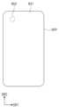
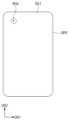
도 1a 및 도 1b를 참조하면, 표시 장치(EA)는 전기적 신호에 따라 활성화되는 장치일 수 있다. 표시 장치(EA)는 다양한 실시예들을 포함할 수 있다. 예를 들어, 표시 장치(EA)는 텔레비전, 모니터, 또는 외부 광고판과 같은 대형 전자장치를 비롯하여, 퍼스널 컴퓨터, 노트북 컴퓨터, 개인 디지털 단말기, 자동차 내비게이션 유닛, 게임기, 휴대용 전자 기기, 및 카메라와 같은 중소형 전자 장치 등에 사용될 수도 있다. 또한, 이것들은 단지 실시예로서 제시된 것들로서, 본 발명의 개념에서 벗어나지 않은 이상 다른 전자 기기에도 채용될 수 있음은 물론이다. 본 실시예에서, 표시 장치(EA)는 스마트 폰으로 예시적으로 도시되었다.Referring to FIGS. 1A and 1B, the display device (EA) may be a device activated according to an electrical signal. The display device (EA) may include various embodiments. For example, the display device (EA) may be used in large electronic devices such as televisions, monitors, or external billboards, as well as small and medium-sized electronic devices such as personal computers, notebook computers, personal digital assistants, car navigation units, game consoles, portable electronic devices, and cameras. In addition, these are presented only as examples, and it goes without saying that the display device (EA) may be employed in other electronic devices as long as it does not depart from the concept of the present invention. In the present embodiment, the display device (EA) is exemplarily illustrated as a smart phone.
표시 장치(EA)는 제1 방향(DR1) 및 제2 방향(DR2) 각각에 평행한 표시면(FS)에 제3 방향(DR3)을 향해 영상(IM)을 표시할 수 있다. 영상(IM)은 동적인 영상은 물론 정지 영상을 포함할 수 있다. 도 1a에서 영상(IM)의 일 예로 시계창 및 아이콘들이 도시되었다. 영상(IM)이 표시되는 표시면(FS)은 표시 장치(EA)의 전면(front surface)과 대응될 수 있으며, 윈도우 패널(WP)의 전면과 대응될 수 있다.The display device (EA) can display an image (IM) toward a third direction (DR3) on a display surface (FS) parallel to each of the first direction (DR1) and the second direction (DR2). The image (IM) can include a still image as well as a moving image. As examples of the image (IM), a clock window and icons are illustrated in Fig. 1a. The display surface (FS) on which the image (IM) is displayed can correspond to the front surface of the display device (EA) and can correspond to the front surface of the window panel (WP).
본 실시예에서는 영상(IM)이 표시되는 방향을 기준으로 각 부재들의 전면(또는 전면)과 배면(또는 하면)이 정의된다. 전면과 배면은 제3 방향(DR3)에서 서로 대향되고, 전면과 배면 각각의 법선 방향은 제3 방향(DR3)과 평행할 수 있다. 한편, 제1 내지 제3 방향들(DR1, DR3, DR3)이 지시하는 방향은 상대적인 개념으로서 다른 방향으로 변환될 수 있다. 이하, 제1 내지 제3 방향들은 제1 내지 제3 방향들(DR1, DR2, DR3)이 각각 지시하는 방향으로 동일한 도면 부호를 참조한다.In this embodiment, the front (or front side) and the back (or bottom side) of each member are defined based on the direction in which the image (IM) is displayed. The front and the back side are opposite to each other in the third direction (DR3), and the normal direction of each of the front and the back side can be parallel to the third direction (DR3). Meanwhile, the directions indicated by the first to third directions (DR1, DR3, DR3) are relative concepts and can be converted to other directions. Hereinafter, the first to third directions refer to the same drawing symbols as the directions indicated by the first to third directions (DR1, DR2, DR3), respectively.
본 발명의 일 실시예에 따른 표시 장치(EA)는 외부에서 인가되는 사용자의 입력을 감지할 수 있다. 사용자의 입력은 사용자 신체의 일부, 광, 열, 또는 압력 등 다양한 형태의 외부 입력들을 포함한다. 또한, 표시 장치(EA)는 표시 장치(EA)의 구조에 따라 표시 장치(EA)의 측면이나 배면에 인가되는 사용자의 입력을 감지할 수도 있으며, 어느 하나의 실시예로 한정되지 않는다.The display device (EA) according to one embodiment of the present invention can detect a user's input applied from the outside. The user's input includes various forms of external input, such as a part of the user's body, light, heat, or pressure. In addition, the display device (EA) can detect a user's input applied to a side or back surface of the display device (EA) depending on the structure of the display device (EA), and is not limited to any one embodiment.
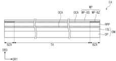
표시 장치(EA)는 윈도우 패널(WP), 반사 방지 패널(RPP), 표시 모듈(DM), 전자 모듈(SS), 및 하우징(HU)을 포함할 수 있다. 본 실시예에서, 윈도우 패널(WP)와 하우징(HU)은 결합되어 표시 장치(EA)의 외관을 구성한다.The display device (EA) may include a window panel (WP), an anti-reflection panel (RPP), a display module (DM), an electronic module (SS), and a housing (HU). In the present embodiment, the window panel (WP) and the housing (HU) are combined to form the appearance of the display device (EA).
윈도우 패널(WP)는 광학적으로 투명한 절연 물질을 포함할 수 있다. 예를 들어, 윈도우 패널(WP)은 유리 또는 플라스틱을 포함할 수 있다. 윈도우 패널(WP)은 다층구조 또는 단층구조를 가질 수 있다. 예를 들어, 윈도우 패널(WP)은 접착제로 결합된 복수 개의 플라스틱 필름을 포함하거나, 접착제로 결합된 유리 기판과 플라스틱 필름을 포함할 수 있다.The window panel (WP) may include an optically transparent insulating material. For example, the window panel (WP) may include glass or plastic. The window panel (WP) may have a multilayer structure or a single layer structure. For example, the window panel (WP) may include a plurality of plastic films bonded with an adhesive, or may include a glass substrate and a plastic film bonded with an adhesive.
윈도우 패널(WP)의 전면(FS)은 상술한 바와 같이, 표시 장치(EA)의 전면을 정의한다. 투과 영역(TA)은 광학적으로 투명한 영역일 수 있다. 예를 들어, 투과 영역(TA)은 약 90% 이상의 가시광선 투과율을 가진 영역일 수 있다.The front surface (FS) of the window panel (WP) defines the front surface of the display device (EA), as described above. The transmissive area (TA) may be an optically transparent area. For example, the transmissive area (TA) may be an area having a visible light transmittance of about 90% or more.
베젤 영역(BZA)은 투과 영역(TA)에 비해 상대적으로 광 투과율이 낮은 영역일 수 있다. 베젤 영역(BZA)은 투과 영역(TA)의 형상을 정의한다. 베젤 영역(BZA)은 투과 영역(TA)에 인접하며, 투과 영역(TA)을 에워쌀 수 있다.The bezel area (BZA) may be an area with relatively low light transmittance compared to the transmissive area (TA). The bezel area (BZA) defines the shape of the transmissive area (TA). The bezel area (BZA) is adjacent to the transmissive area (TA) and may surround the transmissive area (TA).
베젤 영역(BZA)은 소정의 컬러를 가질 수 있다. 베젤 영역(BZA)은 표시 모듈(DM)의 주변 영역(NAA)을 커버하여 주변 영역(NAA)이 외부에서 시인되는 것을 차단할 수 있다. 한편, 이는 예시적으로 도시된 것이고, 본 발명의 일 실시예에 따른 윈도우 패널(WP)에 있어서, 베젤 영역(BZA)은 생략될 수도 있다.The bezel area (BZA) may have a predetermined color. The bezel area (BZA) may cover the peripheral area (NAA) of the display module (DM) to block the peripheral area (NAA) from being viewed from the outside. Meanwhile, this is illustrated as an example, and in the window panel (WP) according to one embodiment of the present invention, the bezel area (BZA) may be omitted.
반사 방지 패널(RPP)은 윈도우 패널(WP) 아래에 배치될 수 있다. 반사 방지 패널(RPP)은 윈도우 패널(WP)의 상측으로부터 입사되는 외부광의 반사율을 감소시킨다.An anti-reflection panel (RPP) can be placed under the window panel (WP). The anti-reflection panel (RPP) reduces the reflectance of external light incident from the upper side of the window panel (WP).
표시 모듈(DM)은 영상(IM)을 표시하고 외부 입력을 감지할 수 있다. 표시 모듈(DM)은 액티브 영역(AA) 및 주변 영역(NAA)을 포함하는 전면(IS)을 포함한다. 액티브 영역(AA)은 전기적 신호에 따라 활성화되는 영역일 수 있다.A display module (DM) can display an image (IM) and detect external input. The display module (DM) includes a front surface (IS) that includes an active area (AA) and a peripheral area (NAA). The active area (AA) can be an area that is activated according to an electrical signal.
본 실시예에서, 액티브 영역(AA)은 영상(IM)이 표시되는 영역이며, 동시에 외부 입력이 감지되는 영역일 수 있다. 투과 영역(TA)은 적어도 액티브 영역(AA)과 중첩한다. 예를 들어, 투과 영역(TA)은 액티브 영역(AA)의 전면 또는 적어도 일부와 중첩한다. 이에 따라, 사용자는 투과 영역(TA)을 통해 영상(IM)을 시인하거나, 외부 입력을 제공할 수 있다. 다만, 이는 예시적으로 도시한 것이고, 액티브 영역(AA) 내에서 영상(IM)이 표시되는 영역과 외부 입력이 감지되는 영역이 서로 분리될 수도 있으며, 어느 하나의 실시예로 한정되지 않는다.In the present embodiment, the active area (AA) is an area where the image (IM) is displayed and may also be an area where an external input is detected. The transparent area (TA) overlaps at least the active area (AA). For example, the transparent area (TA) overlaps the entire surface or at least a portion of the active area (AA). Accordingly, a user may view the image (IM) or provide an external input through the transparent area (TA). However, this is merely an example, and the area where the image (IM) is displayed and the area where an external input is detected may be separated from each other within the active area (AA), and is not limited to any one embodiment.
주변 영역(NAA)은 베젤 영역(BZA)에 의해 커버되는 영역일 수 있다. 주변 영역(NAA)은 액티브 영역(AA)에 인접한다. 주변 영역(NAA)은 액티브 영역(AA)을 에워쌀 수 있다. 주변 영역(NAA)에는 액티브 영역(AA)을 구동하기 위한 구동 회로나 구동 배선 등이 배치될 수 있다.The peripheral area (NAA) may be an area covered by the bezel area (BZA). The peripheral area (NAA) is adjacent to the active area (AA). The peripheral area (NAA) may surround the active area (AA). A driving circuit or driving wiring for driving the active area (AA) may be arranged in the peripheral area (NAA).
본 실시예에서, 표시 모듈(DM)은 액티브 영역(AA) 및 주변 영역(NAA)이 윈도우 패널(WP)를 향하는 평탄한 상태로 조립된다. 다만 이는 예시적으로 도시한 것이고, 표시 모듈(DM)의 주변 영역(NAA)의 일부분은 휘어질 수 있다. 이 때, 주변 영역(NAA) 중 일부는 표시 장치(EA)의 배면을 향하게 되어, 표시 장치(EA) 전면에서의 베젤 영역(BZA)이 감소될 수 있다. 또는, 표시 모듈(DM)은 액티브 영역(AA)의 일부도 휘어진 상태로 조립될 수도 있다. 또는, 본 발명의 일 실시예에 따른 표시 모듈(DM)에 있어서 주변 영역(NAA)은 생략될 수도 있다.In the present embodiment, the display module (DM) is assembled in a flat state with the active area (AA) and the peripheral area (NAA) facing the window panel (WP). However, this is merely an example, and a part of the peripheral area (NAA) of the display module (DM) may be curved. In this case, a part of the peripheral area (NAA) may face the back of the display device (EA), so that the bezel area (BZA) on the front of the display device (EA) may be reduced. Alternatively, the display module (DM) may be assembled in a state in which a part of the active area (AA) is also curved. Alternatively, the peripheral area (NAA) may be omitted in the display module (DM) according to one embodiment of the present invention.
표시 모듈(DM)은 표시 패널(DP), 입력 감지층(ISL), 및 구동 회로(DC)를 포함한다.The display module (DM) includes a display panel (DP), an input sensing layer (ISL), and a driver circuit (DC).
표시 패널(DP)은 실질적으로 영상(IM)을 생성하는 구성일 수 있다. 표시 패널(DP)이 생성하는 영상(IM)은 투과 영역(TA)을 통해 외부에서 사용자에게 시인된다.The display panel (DP) may be configured to substantially generate an image (IM). The image (IM) generated by the display panel (DP) is viewed by a user from the outside through a transparent area (TA).
입력 감지층(ISL)은 외부에서 인가되는 외부 입력을 감지한다. 상술한 바와 같이, 입력 감지층(ISL)은 윈도우 패널(WP)에 제공되는 외부 입력을 감지할 수 있다.The input sensing layer (ISL) detects external input applied from the outside. As described above, the input sensing layer (ISL) can detect external input provided to the window panel (WP).
구동 회로(DC)는 표시 패널(DP) 및 입력 감지층(ISL)과 전기적으로 연결된다. 구동 회로(DC)는 메인 회로 기판(MB), 제1 회로 기판(CF1), 및 제2 회로 기판(CF2)을 포함한다.The driving circuit (DC) is electrically connected to the display panel (DP) and the input sensing layer (ISL). The driving circuit (DC) includes a main circuit board (MB), a first circuit board (CF1), and a second circuit board (CF2).
제1 회로 기판(CF1)은 표시 패널(DP)과 전기적으로 연결된다. 제1 회로 기판(CF1)은 표시 패널(DP)과 메인 회로 기판(MB)을 연결할 수 있다. 본 실시예에서, 제1 회로 기판(CF1)은 연성 회로 필름으로 도시되었다. 다만, 이는 예시적으로 도시한 것이고, 제1 회로 기판(CF1)은 메인 회로 기판(MB)과 연결되지 않을 수도 있고, 제1 회로 기판(CF1)은 리지드한 기판일 수도 있다.The first circuit board (CF1) is electrically connected to the display panel (DP). The first circuit board (CF1) can connect the display panel (DP) and the main circuit board (MB). In the present embodiment, the first circuit board (CF1) is illustrated as a flexible circuit film. However, this is illustrated as an example, and the first circuit board (CF1) may not be connected to the main circuit board (MB), and the first circuit board (CF1) may be a rigid board.
제1 회로 기판(CF1)은 주변 영역(NAA)에 배치된 표시 패널(DP)의 패드들(표시 패드들)에 접속될 수 있다. 제1 회로 기판(CF1)은 표시 패널(DP)을 구동하기 위한 전기적 신호를 표시 패널(DP)에 제공한다. 전기적 신호는 제1 회로 기판(CF1)에서 생성되거나 메인 회로 기판(MB)에서 생성된 것일 수 있다.The first circuit board (CF1) can be connected to pads (display pads) of a display panel (DP) arranged in a peripheral area (NAA). The first circuit board (CF1) provides an electrical signal for driving the display panel (DP) to the display panel (DP). The electrical signal may be generated in the first circuit board (CF1) or in the main circuit board (MB).
제2 회로 기판(CF2)은 입력 감지층(ISL)과 전기적으로 연결된다. 제2 회로 기판(CF2)은 입력 감지층(ISL)과 메인 회로 기판(MB)을 연결할 수 있다. 본 실시예에서, 제2 회로 기판(CF2)은 연성 회로 필름으로 도시되었다. 다만, 이는 예시적으로 도시한 것이고, 제2 회로 기판(CF2)은 메인 회로 기판(MB)과 연결되지 않을 수도 있고, 제2 회로 기판(CF2)은 리지드한 기판일 수도 있다.The second circuit board (CF2) is electrically connected to the input sensing layer (ISL). The second circuit board (CF2) can connect the input sensing layer (ISL) and the main circuit board (MB). In the present embodiment, the second circuit board (CF2) is illustrated as a flexible circuit film. However, this is illustrated as an example, and the second circuit board (CF2) may not be connected to the main circuit board (MB), and the second circuit board (CF2) may be a rigid board.
제2 회로 기판(CF2)은 주변 영역(NAA)에 배치된 입력 감지층(ISL)의 패드들(감지 패드들)에 접속될 수 있다. 제2 회로 기판(CF2)은 입력 감지층(ISL)을 구동하기 위한 전기적 신호를 입력 감지층(ISL)에 제공한다. 전기적 신호는 제2 회로 기판(CF2)에서 생성되거나 메인 회로 기판(MB)에서 생성된 것일 수 있다.The second circuit board (CF2) can be connected to pads (sensing pads) of the input sensing layer (ISL) arranged in the peripheral area (NAA). The second circuit board (CF2) provides an electrical signal to the input sensing layer (ISL) for driving the input sensing layer (ISL). The electrical signal can be generated in the second circuit board (CF2) or in the main circuit board (MB).
메인 회로 기판(MB)은 표시 모듈(DM)을 구동하기 위한 각종 구동 회로나 전원 공급을 위한 커넥터 등을 포함할 수 있다. 제1 회로 기판(CF1)과 제2 회로 기판(CF2)은 각각 메인 회로 기판(MB)에 접속될 수 있다. 본 발명에 따르면, 하나의 메인 회로 기판(MB)을 통해 표시 모듈(DM)을 용이하게 제어할 수 있다. 다만, 이는 예시적으로 도시한 것이고, 본 발명의 일 실시예에 따른 표시 모듈(DM)에 있어서, 표시 패널(DP)과 입력 감지층(ISL)은 서로 다른 메인 회로 기판에 연결될 수도 있고, 제1 회로 기판(CF1)과 제2 회로 기판(CF2) 중 어느 하나는 메인 회로 기판(MB)에 연결되지 않을 수도 있으며, 어느 하나의 실시예로 한정되지 않는다.The main circuit board (MB) may include various driving circuits for driving the display module (DM), connectors for power supply, etc. The first circuit board (CF1) and the second circuit board (CF2) may each be connected to the main circuit board (MB). According to the present invention, the display module (DM) can be easily controlled through one main circuit board (MB). However, this is merely an example, and in the display module (DM) according to one embodiment of the present invention, the display panel (DP) and the input sensing layer (ISL) may be connected to different main circuit boards, and either the first circuit board (CF1) or the second circuit board (CF2) may not be connected to the main circuit board (MB), and the present invention is not limited to any one embodiment.
전자 모듈(SS)은 표시 모듈(DM) 아래에 배치될 수 있다. 전자 모듈(SS)은 표시 패널(DP) 아래에 배치될 수 있다. 평면 상에서 전자 모듈(SS)은 액티브 영역(AA)과 중첩하여 배치될 수 있다. 따라서, 베젤 영역(BZA)에 전자 모듈(SS)이 배치될 공간이 생략될 수 있고, 베젤 영역(BZA)의 면적의 증가가 방지될 수 있다.The electronic module (SS) can be arranged under the display module (DM). The electronic module (SS) can be arranged under the display panel (DP). On a plane, the electronic module (SS) can be arranged to overlap the active area (AA). Accordingly, the space where the electronic module (SS) is arranged in the bezel area (BZA) can be omitted, and an increase in the area of the bezel area (BZA) can be prevented.
전자 모듈(SS)은 투과 영역(TA)을 통해 전달되는 외부 입력을 수신하거나, 투과 영역(TA)을 통해 출력을 제공할 수 있다. 전자 모듈(SS)은 적외선 감지 센서, 근접 센서, 카메라, 스피커, 광 감지 센서, 및 열 감지 센서 중 적어도 어느 하나를 포함할 수 있다. 전자 모듈(SS)은 복수의 구성들을 포함할 수도 있으며, 어느 하나의 실시예로 한정되지 않는다.The electronic module (SS) can receive external input transmitted through the transparent area (TA), or provide output through the transparent area (TA). The electronic module (SS) can include at least one of an infrared detection sensor, a proximity sensor, a camera, a speaker, a light detection sensor, and a heat detection sensor. The electronic module (SS) can include a plurality of components, and is not limited to any one embodiment.
하우징(HU)은 윈도우 패널(WP)과 결합된다. 하우징(HU)은 윈도우 패널(WP)과 결합되어 소정의 내부 공간을 제공한다. 표시 모듈(DM) 및 전자 모듈(SS)은 내부 공간에 수용될 수 있다.The housing (HU) is coupled with the window panel (WP). The housing (HU) is coupled with the window panel (WP) to provide a predetermined internal space. A display module (DM) and an electronic module (SS) can be accommodated in the internal space.
하우징(HU)은 상대적으로 높은 강성을 가진 물질을 포함할 수 있다. 예를 들어, 하우징(HU)은 유리, 플라스틱, 또는 금속을 포함하거나, 이들의 조합으로 구성된 복수 개의 프레임 및/또는 플레이트를 포함할 수 있다. 하우징(HU)은 내부 공간에 수용된 표시 장치(EA)의 구성들을 외부 충격으로부터 안정적으로 보호할 수 있다.The housing (HU) may include a material having relatively high rigidity. For example, the housing (HU) may include a plurality of frames and/or plates made of glass, plastic, or metal, or a combination thereof. The housing (HU) may reliably protect the components of the display device (EA) accommodated in the internal space from external impact.
도 2a 내지 도 2d는 본 발명의 일 실시예에 따른 표시 장치의 단면도들이다.FIGS. 2A to 2D are cross-sectional views of a display device according to one embodiment of the present invention.
도 2a 내지 도 2d는 제1 방향(DR1)과 제3 방향(DR3)이 정의하는 단면을 도시하였다. 도 2a 내지 도 2d는 표시 장치(EA)를 구성하는 기능성 부재들의 적층관계를 설명하기 위해 단순하게 도시되었다.Figures 2a to 2d illustrate cross sections defined by the first direction (DR1) and the third direction (DR3). Figures 2a to 2d are simply illustrated to explain the stacking relationship of functional members constituting the display device (EA).
본 발명의 일 실시예에 따른 표시 장치(EA)는 표시 패널, 입력 감지 센서, 반사 방지 부재(anti-reflector), 및 윈도우를 포함할 수 있다. 표시 패널, 입력 감지 센서, 반사 방지 부재, 및 윈도우 중 적어도 일부의 구성들은 연속공정에 의해 형성되거나, 적어도 일부의 구성들은 접착부재를 통해 서로 결합될 수 있다. 도 2a 내지 도 2d에는 접착부재로써 광학 투명 접착부재(OCA)가 예시적으로 도시되었다. 이하에서 설명되는 접착부재는 통상의 접착제 또는 점착제를 포함할 수 있다. 본 발명의 일 실시예에서 반사 방지 부재 및 윈도우는 다른 구성으로 대체되거나 생략될 수 있다.A display device (EA) according to one embodiment of the present invention may include a display panel, an input detection sensor, an anti-reflector, and a window. At least some of the components of the display panel, the input detection sensor, the anti-reflector, and the window may be formed by a continuous process, or at least some of the components may be bonded to each other via an adhesive member. In FIGS. 2A to 2D , an optically transparent adhesive member (OCA) is exemplarily illustrated as an adhesive member. The adhesive member described below may include a typical adhesive or pressure-sensitive adhesive. In one embodiment of the present invention, the anti-reflector and the window may be replaced with other components or omitted.
도 2a 내지 도 2d에 있어서, 입력 감지 센서, 반사 방지 부재, 및 윈도우 중 다른 구성과 연속공정을 통해 형성된 해당 구성은 "층"으로 표현된다. 입력 감지 센서, 반사 방지 부재, 및 윈도우 중 다른 구성과 접착부재를 통해 결합된 구성은 "패널"로 표현된다. 패널은 베이스면을 제공하는 베이스층, 예컨대 합성수지 필름, 복합재료 필름, 유리 기판 등을 포함하지만, "층"은 상기 베이스층이 생략될 수 있다. 다시 말해, "층"으로 표현되는 상기 유닛들은 다른 유닛이 제공하는 베이스면 상에 배치된다.In FIGS. 2A to 2D, the input detection sensor, the anti-reflection member, and the other components among the windows formed through a continuous process are expressed as a "layer." The other components among the input detection sensor, the anti-reflection member, and the window joined through an adhesive member are expressed as a "panel." The panel includes a base layer providing a base surface, such as a synthetic resin film, a composite material film, a glass substrate, or the like, but the "layer" may omit the base layer. In other words, the units expressed as "layers" are arranged on base surfaces provided by other units.
이하, 입력 감지 센서, 반사 방지 부재, 윈도우는 베이스층의 유/무에 따라 입력 감지 패널(ISP), 반사 방지 패널(RPP), 윈도우 패널(WP) 또는 입력 감지층(ISL), 반사 방지층(RPL), 윈도우층(WL)로 지칭될 수 있다.Hereinafter, the input detection sensor, anti-reflection member, and window may be referred to as an input detection panel (ISP), an anti-reflection panel (RPP), a window panel (WP), or an input detection layer (ISL), an anti-reflection layer (RPL), and a window layer (WL) depending on the presence or absence of a base layer.
도 2a에 도시된 것과 같이, 표시 장치(EA)는 표시 패널(DP), 입력 감지층(ISL), 반사 방지 패널(RPP), 및 윈도우 패널(WP)을 포함할 수 있다. 입력 감지층(ISL)은 표시 패널(DP)에 직접 배치된다. 본 명세서에서 "B의 구성이 A의 구성 상에 직접 배치된다"는 것은 A의 구성과 B의 구성 사이에 별도의 접착층/접착 부재가 배치되지 않는 것을 의미한다. B 구성은 A 구성이 형성된 이후에 A구성이 제공하는 베이스면 상에 연속공정을 통해 형성된다.As illustrated in FIG. 2A, the display device (EA) may include a display panel (DP), an input sensing layer (ISL), an anti-reflection panel (RPP), and a window panel (WP). The input sensing layer (ISL) is directly disposed on the display panel (DP). In the present specification, "the configuration of B is directly disposed on the configuration of A" means that no separate adhesive layer/adhesive member is disposed between the configuration of A and the configuration of B. The configuration of B is formed on a base surface provided by the configuration of A through a continuous process after the configuration of A is formed.
표시 패널(DP)과 표시 패널(DP) 상에 직접 배치된 입력 감지층(ISL)을 포함하여 표시 모듈(DM)로 정의될 수 있다. 표시 모듈(DM)과 반사 방지 패널(RPP) 사이, 반사 방지 패널(RPP)과 윈도우 패널(WP) 사이 각각에 광학 투명 접착부재(OCA)가 배치된다.A display module (DM) may be defined including a display panel (DP) and an input sensing layer (ISL) directly disposed on the display panel (DP). An optically clear adhesive (OCA) is disposed between the display module (DM) and an anti-reflection panel (RPP), and between the anti-reflection panel (RPP) and a window panel (WP).
표시 패널(DP)은 영상을 생성하고, 입력 감지층(ISL)은 외부입력(예컨대, 터치 이벤트)의 좌표정보를 획득한다. 별도로 도시하지 않았으나, 본 발명의 일 실시예에 따른 표시 모듈(DM)은 표시 패널(DP)의 하면에 배치된 보호부재를 더 포함할 수 있다. 보호부재와 표시 패널(DP)은 접착부재를 통해 결합될 수 있다. 이하에서 설명되는 도 2b 내지 도 2d의 표시 장치들(EA) 역시 보호부재를 더 포함할 수 있다.The display panel (DP) generates an image, and the input sensing layer (ISL) obtains coordinate information of an external input (e.g., a touch event). Although not illustrated separately, the display module (DM) according to an embodiment of the present invention may further include a protective member arranged on a lower surface of the display panel (DP). The protective member and the display panel (DP) may be combined via an adhesive member. The display devices (EA) of FIGS. 2B to 2D described below may also further include a protective member.
본 발명의 일 실시예에 따른 표시 패널(DP)은 발광형 표시 패널일 수 있고, 특별히 제한되지 않는다. 예컨대, 표시 패널(DP)은 유기발광 표시 패널 또는 퀀텀닷 발광 표시 패널일 수 있다. 유기발광 표시 패널의 발광층은 유기발광물질을 포함할 수 있다. 퀀텀닷 발광 표시 패널의 발광층은 퀀텀닷, 및 퀀텀로드 등을 포함할 수 있다. 이하, 표시 패널(DP)은 유기발광 표시 패널로 설명된다.The display panel (DP) according to one embodiment of the present invention may be a light-emitting display panel, and is not particularly limited thereto. For example, the display panel (DP) may be an organic light-emitting display panel or a quantum dot light-emitting display panel. The light-emitting layer of the organic light-emitting display panel may include an organic light-emitting material. The light-emitting layer of the quantum dot light-emitting display panel may include quantum dots, quantum rods, and the like. Hereinafter, the display panel (DP) is described as an organic light-emitting display panel.
반사 방지 패널(RPP)은 윈도우 패널(WP)의 상측으로부터 입사되는 외부광의 반사율을 감소시킨다. 본 발명의 일 실시예에 따른 반사 방지 패널(RPP)은 위상지연자(retarder) 및 편광자(polarizer)를 포함할 수 있다. 위상지연자는 필름타입 또는 액정 코팅타입일 수 있고, 위상지연자 및/또는 위상지연자를 포함할 수 있다. 편광자 역시 필름타입으로, 연신형 합성수지 필름을 포함할 수 있다. 위상지연자 및 편광자는 보호필름을 더 포함할 수 있다. 위상지연자(retarder) 및 편광자(polarizer) 자체 또는 보호필름이 반사 방지 패널(RPP)의 베이스층으로 정의될 수 있다.An anti-reflection panel (RPP) reduces the reflectivity of external light incident from the upper side of a window panel (WP). An anti-reflection panel (RPP) according to one embodiment of the present invention may include a retarder and a polarizer. The retarder may be a film type or a liquid crystal coating type, Phase delayer and/or A phase retarder may be included. The polarizer may also be of film type and may include a stretchable synthetic resin film. The phase retarder and the polarizer may further include a protective film. The phase retarder and the polarizer themselves or the protective film may be defined as a base layer of an anti-reflection panel (RPP).
본 발명의 일 실시예에 따른 윈도우 패널(WP)은 베이스층(WP-BS)및 차광패턴(WP-BZ)을 포함한다. 베이스층(WP-BS)는 유리 기판 및/또는 합성수지 필름 등을 포함할 수 있다. 베이스층(WP-BS)은 단층으로 제한되지 않는다. 베이스층(WP-BS)은 접착부재로 결합된 2 이상의 필름들을 포함할 수 있다.A window panel (WP) according to one embodiment of the present invention includes a base layer (WP-BS) and a shading pattern (WP-BZ). The base layer (WP-BS) may include a glass substrate and/or a synthetic resin film. The base layer (WP-BS) is not limited to a single layer. The base layer (WP-BS) may include two or more films bonded together by an adhesive.
차광패턴(WP-BZ)은 베이스층(WP-BS)에 부분적으로 중첩한다. 차광패턴(WP-BZ)은 베이스층(WP-BS)의 배면에 배치되고, 차광패턴(WP-BZ)은 실질적으로 표시 장치(EA)의 베젤 영역(BZA)을 정의할 수 있다. 차광패턴(WP-BZ)이 미배치된 영역은 표시 장치(EA)의 투과 영역(TA)을 정의할 수 있다. 윈도우 패널(WP)로 한정할 때, 차광패턴(WP-BZ)이 배치된 영역은 윈도우 패널(WP)의 차광영역으로 정의되고, 차광패턴(WP-BZ)이 미배치된 영역은 윈도우 패널(WP)의 투과영역으로 정의된다.The shading pattern (WP-BZ) partially overlaps the base layer (WP-BS). The shading pattern (WP-BZ) is arranged on the back surface of the base layer (WP-BS), and the shading pattern (WP-BZ) can substantially define a bezel area (BZA) of the display device (EA). An area where the shading pattern (WP-BZ) is not arranged can define a transparent area (TA) of the display device (EA). When limited to the window panel (WP), the area where the shading pattern (WP-BZ) is arranged is defined as a shading area of the window panel (WP), and the area where the shading pattern (WP-BZ) is not arranged is defined as a transparent area of the window panel (WP).
차광패턴(WP-BZ)은 다층구조를 가질 수 있다. 다층구조는 유색의 컬러층과 검정의 차광층을 포함할 수 있다. 유색의 컬러층과 검정의 차광층은 증착, 인쇄, 코팅 공정을 통해 형성될 수 있다. 별도로 도시하지는 않았으나, 윈도우 패널(WP)은 베이스층(WP-BS)의 전면에 배치된 기능성 코팅층을 더 포함할 수 있다. 기능성 코팅층은 지문 방지층, 반사 방지층, 및 하드 코팅층 등을 포함할 수 있다. 이하에서 참조되는 도 2b 내지 도 2d에 있어서, 윈도우 패널(WP) 및 윈도우층(WL)은 베이스층(WP-BS) 및 차광패턴(WP-BZ)의 구분 없이 간략히 도시되었다.The shading pattern (WP-BZ) may have a multilayer structure. The multilayer structure may include a colored color layer and a black shading layer. The colored color layer and the black shading layer may be formed through a deposition, printing, or coating process. Although not illustrated separately, the window panel (WP) may further include a functional coating layer disposed on the entire surface of the base layer (WP-BS). The functional coating layer may include an anti-fingerprint layer, an anti-reflection layer, and a hard coating layer. In FIGS. 2b to 2d referred to below, the window panel (WP) and the window layer (WL) are briefly illustrated without distinction between the base layer (WP-BS) and the shading pattern (WP-BZ).
도 2b 및 도 2c에 도시된 것과 같이, 표시 장치(EA)는 표시 패널(DP), 입력 감지 패널(ISP), 반사 방지 패널(RPP), 및 윈도우 패널(WP)을 포함할 수 있다. 입력 감지 패널(ISP)과 반사 방지 패널(RPP)의 적층 순서는 변경될 수 있다.As illustrated in FIGS. 2b and 2c, the display device (EA) may include a display panel (DP), an input detection panel (ISP), an anti-reflection panel (RPP), and a window panel (WP). The stacking order of the input detection panel (ISP) and the anti-reflection panel (RPP) may be changed.
도 2d에 도시된 것과 같이, 표시 장치(EA)는 표시 패널(DP), 입력 감지층(ISL), 반사 방지층(RPL), 및 윈도우층(WL)을 포함할 수 있다. 도 2a에 도시된 표시 장치(EA) 대비 광학 투명 접착 부재들(OCA)이 생략되고, 표시 패널(DP)에 제공하는 베이스면 상에 입력 감지층(ISL), 반사 방지층(RPL), 및 윈도우층(WL)이 연속공정으로 형성되었다. 입력 감지층(ISL)과 반사 방지층(RPL)의 적층 순서는 변경될 수 있다.As illustrated in FIG. 2d, the display device (EA) may include a display panel (DP), an input sensing layer (ISL), an anti-reflection layer (RPL), and a window layer (WL). Compared to the display device (EA) illustrated in FIG. 2a, optically transparent adhesive members (OCA) are omitted, and the input sensing layer (ISL), the anti-reflection layer (RPL), and the window layer (WL) are formed in a continuous process on a base surface provided to the display panel (DP). The stacking order of the input sensing layer (ISL) and the anti-reflection layer (RPL) may be changed.
도 3a는 본 발명의 일 실시예에 따른 반사 방지 패널의 평면도이다. 도 3b는 본 발명의 일 실시예에 따른 반사 방지 패널의 평면도이다. 이하 설명되는 반사 방지 패널(RPP)은 방사 방지층(PRL, 도 2d 참조)에도 동일하게 적용될 수 있다.Fig. 3a is a plan view of an anti-reflection panel according to one embodiment of the present invention. Fig. 3b is a plan view of an anti-reflection panel according to one embodiment of the present invention. The anti-reflection panel (RPP) described below can be equally applied to a radiation prevention layer (PRL, see Fig. 2d).
도 3a 및 도 3b를 참조하면, 반사 방지 패널(RPP)은 제1 영역(RA1) 및 제2 영역(RA2)을 포함할 수 있다. 제1 영역(RA1)은 제2 영역(RA2)을 에워쌀 수 있다. 제2 영역(RA2)은 원형 형상을 가질 수 있다. 제2 영역(RA2)은 평면 상에서 전자 모듈(SS)과 중첩하는 영역일 수 있다.Referring to FIGS. 3A and 3B, the anti-reflection panel (RPP) may include a first region (RA1) and a second region (RA2). The first region (RA1) may surround the second region (RA2). The second region (RA2) may have a circular shape. The second region (RA2) may be a region that overlaps the electronic module (SS) on a plane.
제1 영역(RA1)은 제1 투과율을 갖고, 제2 영역(RA2)은 제2 투과율을 가질 수 있다. 상기 제2 투과율은 상기 제1 투과율보다 높을 수 있다. 예를 들어, 전자 모듈(SS)이 적외선 감지 센서인 경우, 적외선 파장 대역에서 상기 제2 투과율은 상기 제1 투과율보다 높을 수 있다. 본 발명의 실시예에 따르면, 전자 모듈(SS)과 중첩하는 영역의 투과율이 향상됨에 따라, 전자 모듈(SS)의 센싱 감도가 보다 향상될 수 있다.The first region (RA1) may have a first transmittance, and the second region (RA2) may have a second transmittance. The second transmittance may be higher than the first transmittance. For example, when the electronic module (SS) is an infrared detection sensor, the second transmittance may be higher than the first transmittance in an infrared wavelength band. According to an embodiment of the present invention, as the transmittance of the region overlapping the electronic module (SS) is improved, the sensing sensitivity of the electronic module (SS) may be further improved.
전자 모듈(SS)이 적외선 감지 센서인 경우, 전자 모듈(SS)은 발광 모듈 및 수광 모듈을 포함할 수 있다. 상기 발광 모듈은 적외광을 출력하고, 상기 수광 모듈은 적외광을 감지할 수 있다. 상기 수광 모듈은 CMOS 센서를 포함할 수 있다. 상기 발광 모듈에서 생성된 적외광이 출력된 후, 외부 물체, 예를 들어 사용자의 얼굴 또는 손가락에 의해 반사되고, 반사된 적외광이 상기 수광 모듈로 입사될 수 있다.When the electronic module (SS) is an infrared detection sensor, the electronic module (SS) may include a light-emitting module and a light-receiving module. The light-emitting module may output infrared light, and the light-receiving module may detect infrared light. The light-receiving module may include a CMOS sensor. After the infrared light generated by the light-emitting module is output, it may be reflected by an external object, for example, a user's face or finger, and the reflected infrared light may be incident on the light-receiving module.
제2 영역(RA2)의 투과율을 향상시키기 위해, 반사 방지 패널(RPP)의 제2 영역(RA2)에는 다양한 처리가 적용될 수 있다.To improve the transmittance of the second region (RA2), various treatments can be applied to the second region (RA2) of the anti-reflection panel (RPP).
도 3a를 참조하면, 반사 방지 패널(RPP)의 제2 영역(RA2)은 탈색될 수 있다. 예를 들어, 반사 방지 패널(RPP)은 편광자일 수 있고, 반사 방지 패널(RPP)의 제2 영역(RA2)은 탈색될 수 있다. 탈색된 제2 영역(RA2)의 투과율은 탈색되지 않은 제1 영역(RA1)의 투과율보다 높을 수 있다. 또한, 제2 영역(RA2)은 비편광부가 될 수도 있다.Referring to FIG. 3a, the second region (RA2) of the anti-reflection panel (RPP) can be decolorized. For example, the anti-reflection panel (RPP) can be a polarizer, and the second region (RA2) of the anti-reflection panel (RPP) can be decolorized. The transmittance of the decolorized second region (RA2) can be higher than the transmittance of the non-decolorized first region (RA1). In addition, the second region (RA2) can be a non-polarizing portion.
도 3b를 참조하면, 반사 방지 패널(RPP)에는 홀(RHA)이 정의될 수 있다. 홀(RHA)은 제2 영역(RA2, 도 3a 참조)에 정의될 수 있다. 홀(RHA)은 반사 방지 패널(RPP)의 상면으로부터 반사 방지 패널(RPP)의 하면을 연결하여 완전히 관통하는 홀일 수 있다. 하지만, 본 발명이 이에 제한되는 것은 아니다. 예를 들어, 홀(RHA)은 반사 방지 패널(RPP)의 두께 방향의 일부가 제거된 홀일 수도 있다.Referring to FIG. 3b, a hole (RHA) may be defined in the anti-reflection panel (RPP). The hole (RHA) may be defined in a second region (RA2, see FIG. 3a). The hole (RHA) may be a hole that completely penetrates from the upper surface of the anti-reflection panel (RPP) to the lower surface of the anti-reflection panel (RPP). However, the present invention is not limited thereto. For example, the hole (RHA) may be a hole in which a portion in the thickness direction of the anti-reflection panel (RPP) is removed.
도 4a는 본 발명의 일 실시예에 따른 표시 패널의 평면도이다. 도 4b는 본 발명의 일 실시예에 따른 화소의 등가 회로도이다.FIG. 4a is a plan view of a display panel according to one embodiment of the present invention. FIG. 4b is an equivalent circuit diagram of a pixel according to one embodiment of the present invention.
도 4a를 참조하면, 표시 패널(DP)은 베이스층(BS), 복수의 화소들(PX), 복수의 신호 라인들(GL, DL, PL, ECL), 및 복수의 표시 패드들(PDD)을 포함할 수 있다.Referring to FIG. 4a, the display panel (DP) may include a base layer (BS), a plurality of pixels (PX), a plurality of signal lines (GL, DL, PL, ECL), and a plurality of display pads (PDD).
베이스층(BS)은 실리콘 기판, 플라스틱 기판, 유리 기판, 절연 필름, 또는 복수의 절연층들을 포함하는 적층 구조체일 수 있다.The base layer (BS) may be a silicon substrate, a plastic substrate, a glass substrate, an insulating film, or a laminated structure including a plurality of insulating layers.
표시 패널(DP)의 액티브 영역(AA)은 영상이 표시되는 영역이고, 주변 영역(NAA)은 구동 회로나 구동 배선 등이 배치된 영역일 수 있다. 도 4a에서는 표시 패널(DP)의 액티브 영역(AA) 및 주변 영역(NAA)이 표시되었다. 액티브 영역(AA)에는 복수의 화소들(PX)이 배치될 수 있다.The active area (AA) of the display panel (DP) is an area where an image is displayed, and the peripheral area (NAA) may be an area where a driving circuit or driving wiring is arranged. In Fig. 4a, the active area (AA) and the peripheral area (NAA) of the display panel (DP) are shown. A plurality of pixels (PX) may be arranged in the active area (AA).
표시 패널(DP)에는 제1 표시 영역(DA1) 및 제2 표시 영역(DA2)이 정의될 수 있다. 또한, 제1 표시 영역(DA1)은 영상을 표시하는 영역일 수 있다. 제1 표시 영역(DA1)은 제2 표시 영역(DA2)을 에워쌀 수 있다. 따라서, 제1 표시 영역(DA1) 및 제2 표시 영역(DA2)은 표시 패널(DP)의 액티브 영역(AA)을 구성할 수 있다.A first display area (DA1) and a second display area (DA2) may be defined in the display panel (DP). In addition, the first display area (DA1) may be an area that displays an image. The first display area (DA1) may surround the second display area (DA2). Accordingly, the first display area (DA1) and the second display area (DA2) may constitute an active area (AA) of the display panel (DP).
제1 표시 영역(DA1)은 평면 상에서 제1 영역(RA1, 도 3a 참조)과 중첩하는 영역이고, 제2 표시 영역(DA2)은 평면 상에서 제2 영역(RA2, 도 3a 참조)과 중첩하는 영역일 수 있다.The first display area (DA1) may be an area overlapping the first area (RA1, see FIG. 3a) on the plane, and the second display area (DA2) may be an area overlapping the second area (RA2, see FIG. 3a) on the plane.
제1 표시 영역(DA1)의 해상도는 제2 표시 영역(DA2)의 해상도와 상이할 수 있다. 예를 들어, 제2 표시 영역(DA2)의 해상도는 제1 표시 영역(DA1)의 해상도보다 낮을 수 있다. 또한, 제1 표시 영역(DA1)의 반사율은 제2 표시 영역(DA2)의 반사율과 상이할 수 있다. 예를 들어, 제2 표시 영역(DA2)의 반사율은 제1 표시 영역(DA1)의 반사율보다 낮을 수 있다. 상기, 반사율은 외광에 대한 반사율을 의미할 수 있다.The resolution of the first display area (DA1) may be different from the resolution of the second display area (DA2). For example, the resolution of the second display area (DA2) may be lower than the resolution of the first display area (DA1). In addition, the reflectivity of the first display area (DA1) may be different from the reflectivity of the second display area (DA2). For example, the reflectivity of the second display area (DA2) may be lower than the reflectivity of the first display area (DA1). The reflectivity may mean reflectivity for external light.
반사 방지 패널(RPP, 도 3a 참조)의 제2 영역(RA2)의 투과율은 제1 영역(RA1)의 투과율보다 높다. 따라서, 제2 영역(RA2)의 외광 반사 방지 성능은 제1 영역(RA1)의 외광 반사 방지 성능보다 다소 감소될 수 있다. 하지만, 본 발명의 실시예에 따르면, 제2 영역(RA2)에서 외광 반사 방지 성능이 감소되더라도, 제2 표시 영역(DA2)의 반사율을 감소시켜 이를 보완할 수 있다. 표시 패널(DP)의 제1 표시 영역(DA1)과 표시 패널(DP)의 제2 표시 영역(DA2)에서 해상도 및/또는 반사율을 조절하여 상기 외광 반사 방지 성능을 보완할 수 있다.The transmittance of the second area (RA2) of the anti-reflection panel (RPP, see FIG. 3a) is higher than the transmittance of the first area (RA1). Therefore, the external light reflection prevention performance of the second area (RA2) may be somewhat reduced compared to the external light reflection prevention performance of the first area (RA1). However, according to an embodiment of the present invention, even if the external light reflection prevention performance is reduced in the second area (RA2), it can be compensated for by reducing the reflectivity of the second display area (DA2). The external light reflection prevention performance can be compensated for by adjusting the resolution and/or reflectivity in the first display area (DA1) of the display panel (DP) and the second display area (DA2) of the display panel (DP).
복수의 신호 라인들(GL, DL, PL, ECL)은 화소들(PX)에 연결되어 화소들(PX)에 전기적 신호들을 전달한다. 표시 패널(DP)에 포함되는 신호 라인들 중 스캔 라인(GL), 데이터 라인(DL), 전원 라인(PL), 및 발광제어 라인(ECL)을 예시적으로 도시하였다. 다만, 이는 예시적으로 도시한 것이고, 신호 라인들(GL, DL, PL, ECL)은 초기화 전압 라인을 더 포함할 수도 있으며, 어느 하나의 실시예로 한정되지 않는다.A plurality of signal lines (GL, DL, PL, ECL) are connected to pixels (PX) and transmit electrical signals to the pixels (PX). Among the signal lines included in the display panel (DP), a scan line (GL), a data line (DL), a power line (PL), and an emission control line (ECL) are illustrated as examples. However, this is illustrated as examples, and the signal lines (GL, DL, PL, ECL) may further include an initialization voltage line and are not limited to any one embodiment.
도 4b를 참조하면, 복수의 화소들 중 하나의 화소(PX)의 신호 회로도를 확대하여 예시적으로 도시하였다. 도 4b에는 i번째 스캔 라인(GLi) 및 i번째 발광제어 라인(ECLi)에 연결된 화소(PX)를 예시적으로 도시하였다.Referring to Fig. 4b, an enlarged signal circuit diagram of one pixel (PX) among a plurality of pixels is illustrated as an example. Fig. 4b illustrates an example of a pixel (PX) connected to an i-th scan line (GLi) and an i-th emission control line (ECLi).
화소(PX)는 발광 소자(EE) 및 화소 회로(CC)를 포함할 수 있다.A pixel (PX) may include a light-emitting element (EE) and a pixel circuit (CC).
화소 회로(CC)는 복수의 트랜지스터들(T1-T7) 및 커패시터(CP)를 포함할 수 있다. 복수의 트랜지스터들(T1-T7)은 LTPS(Low Temperature Polycrystalline Silicon) 공정 또는 LTPO(Low Temperature Polycrystalline Oxide) 공정을 통해 형성될 수 있다.The pixel circuit (CC) may include a plurality of transistors (T1-T7) and a capacitor (CP). The plurality of transistors (T1-T7) may be formed through a low temperature polycrystalline silicon (LTPS) process or a low temperature polycrystalline oxide (LTPO) process.
화소 회로(CC)는 데이터 신호에 대응하여 발광 소자(EE)에 흐르는 전류량을 제어한다. 발광 소자(EE)는 화소 회로(CC)로부터 제공되는 전류량에 대응하여 소정의 휘도로 발광할 수 있다. 이를 위하여, 제1 전원(ELVDD)의 레벨은 제2 전원(ELVSS)의 레벨보다 높게 설정될 수 있다. 발광 소자(EE)는 유기발광소자 또는 양자점 발광소자를 포함할 수 있다.The pixel circuit (CC) controls the amount of current flowing to the light-emitting element (EE) in response to the data signal. The light-emitting element (EE) can emit light with a predetermined brightness in response to the amount of current provided from the pixel circuit (CC). To this end, the level of the first power supply (ELVDD) can be set higher than the level of the second power supply (ELVSS). The light-emitting element (EE) can include an organic light-emitting element or a quantum dot light-emitting element.
복수의 트랜지스터들(T1-T7) 각각은 입력 전극(또는, 소스 전극), 출력 전극(또는, 드레인 전극), 및 제어 전극(또는, 게이트 전극)을 포함할 수 있다. 본 명세서 내에서 편의상 입력 전극 및 출력 전극 중 어느 하나는 제1 전극으로 지칭되고, 다른 하나는 제2 전극으로 지칭될 수 있다.Each of the plurality of transistors (T1-T7) may include an input electrode (or source electrode), an output electrode (or drain electrode), and a control electrode (or gate electrode). For convenience in this specification, one of the input electrode and the output electrode may be referred to as a first electrode, and the other may be referred to as a second electrode.
제1 트랜지스터(T1)의 제1 전극은 제5 트랜지스터(T5)를 경유하여 제1 전원(ELVDD)에 접속되고, 제1 트랜지스터(T1)의 제2 전극은 제6 트랜지스터(T6)를 경유하여 발광 소자(EE)의 애노드 전극에 접속된다. 제1 트랜지스터(T1)는 본 명세서 내에서 구동 트랜지스터로 지칭될 수 있다.A first electrode of a first transistor (T1) is connected to a first power source (ELVDD) via a fifth transistor (T5), and a second electrode of the first transistor (T1) is connected to an anode electrode of a light-emitting element (EE) via a sixth transistor (T6). The first transistor (T1) may be referred to as a driving transistor within the present specification.
제1 트랜지스터(T1)는 제1 트랜지스터(T1)의 제어 전극에 인가되는 전압에 대응하여 발광 소자(EE)에 흐르는 전류량을 제어한다.The first transistor (T1) controls the amount of current flowing to the light-emitting element (EE) in response to the voltage applied to the control electrode of the first transistor (T1).
제2 트랜지스터(T2)는 데이터 라인(DL)과 제1 트랜지스터(T1)의 제1 전극 사이에 접속된다. 그리고, 제2 트랜지스터(T2)의 제어 전극은 i번째 스캔 라인(GLi)에 접속된다. 제2 트랜지스터(T2)는 i번째 스캔 라인(GLi)으로 i번째 주사 신호가 제공될 때 턴-온되어 데이터 라인(DL)과 제1 트랜지스터(T1)의 제1 전극을 전기적으로 접속시킨다.The second transistor (T2) is connected between the data line (DL) and the first electrode of the first transistor (T1). Further, the control electrode of the second transistor (T2) is connected to the ith scan line (GLi). The second transistor (T2) is turned on when the ith scan signal is provided to the ith scan line (GLi) to electrically connect the data line (DL) and the first electrode of the first transistor (T1).
제3 트랜지스터(T3)는 제1 트랜지스터(T1)의 제2 전극과 제1 트랜지스터(T1)의 제어 전극 사이에 접속된다. 제3 트랜지스터(T3)의 제어 전극은 i번째 스캔 라인(GLi)에 접속된다. 제3 트랜지스터(T3)는 i번째 스캔 라인(GLi)으로 i번째 주사 신호가 제공될 때 턴-온되어 제1 트랜지스터(T1)의 제2 전극과 제1 트랜지스터(T1)의 제어 전극을 전기적으로 접속시킨다. 따라서, 제3 트랜지스터(T3)가 턴-온될 때 제1 트랜지스터(T1)는 다이오드 형태로 접속된다.A third transistor (T3) is connected between the second electrode of the first transistor (T1) and the control electrode of the first transistor (T1). The control electrode of the third transistor (T3) is connected to the ith scan line (GLi). When the ith scan signal is provided to the ith scan line (GLi), the third transistor (T3) is turned on to electrically connect the second electrode of the first transistor (T1) and the control electrode of the first transistor (T1). Therefore, when the third transistor (T3) is turned on, the first transistor (T1) is connected in a diode form.
제4 트랜지스터(T4)는 노드(ND)와 초기화 전원생성부(미도시) 사이에 접속된다. 그리고, 제4 트랜지스터(T4)의 제어 전극은 i-1번째 스캔 라인(GLi-1)에 접속된다. 제4 트랜지스터(T4)는 i-1번째 스캔 라인(GLi-1)으로 i-1번째 주사신호가 제공될 때 턴-온되어 노드(ND)로 초기화전압(Vint)을 제공한다.The fourth transistor (T4) is connected between the node (ND) and an initialization power generation unit (not shown). In addition, the control electrode of the fourth transistor (T4) is connected to the i-1th scan line (GLi-1). The fourth transistor (T4) is turned on when the i-1th scan signal is provided to the i-1th scan line (GLi-1) and provides an initialization voltage (Vint) to the node (ND).
제5 트랜지스터(T5)는 전원 라인(PL)과 제1 트랜지스터(T1)의 제1 전극 사이에 접속된다. 제5 트랜지스터(T5)의 제어 전극은 i번째 발광제어 라인(ECLi)에 접속된다.The fifth transistor (T5) is connected between the power line (PL) and the first electrode of the first transistor (T1). The control electrode of the fifth transistor (T5) is connected to the ith emission control line (ECLi).
제6 트랜지스터(T6)는 제1 트랜지스터(T1)의 제2 전극과 발광 소자(EE)의 애노드전극 사이에 접속된다. 그리고, 제6 트랜지스터(T6)의 제어 전극은 i번째 발광제어 라인(ECLi)에 접속된다.The sixth transistor (T6) is connected between the second electrode of the first transistor (T1) and the anode electrode of the light-emitting element (EE). In addition, the control electrode of the sixth transistor (T6) is connected to the ith light-emitting control line (ECLi).
제7 트랜지스터(T7)는 초기화 전원생성부(미도시)와 발광 소자(EE)의 애노드전극 사이에 접속된다. 그리고, 제7 트랜지스터(T7)의 제어 전극은 i+1번째 스캔 라인(GLi+1)에 접속된다. 이와 같은 제7 트랜지스터(T7)는 i+1번째 스캔 라인(GLi+1)으로 i+1번째 주사신호가 제공될 때 턴-온되어 초기화전압(Vint)을 발광 소자(EE)의 애노드전극으로 제공한다.The seventh transistor (T7) is connected between an initialization power generation unit (not shown) and the anode electrode of the light-emitting element (EE). In addition, the control electrode of the seventh transistor (T7) is connected to the i+1th scan line (GLi+1). The seventh transistor (T7) is turned on when the i+1th scan signal is provided to the i+1th scan line (GLi+1) and provides the initialization voltage (Vint) to the anode electrode of the light-emitting element (EE).
제7 트랜지스터(T7)는 화소(PX)의 블랙 표현 능력을 향상시킬 수 있다. 구체적으로, 제7 트랜지스터(T7)가 턴-온되면 발광 소자(EE)의 기생 커패시터(미도시)가 방전된다. 그러면, 블랙 휘도 구현 시 제1 트랜지스터(T1)로부터의 누설전류에 의하여 발광 소자(EE)가 발광하지 않게되고, 이에 따라 블랙 표현 능력이 향상될 수 있다.The seventh transistor (T7) can improve the black expression capability of the pixel (PX). Specifically, when the seventh transistor (T7) is turned on, the parasitic capacitor (not shown) of the light-emitting element (EE) is discharged. Then, when implementing black luminance, the light-emitting element (EE) does not emit light due to the leakage current from the first transistor (T1), and thus the black expression capability can be improved.
추가적으로, 도 4b에서는 제7 트랜지스터(T7)의 제어 전극이 i+1번째 스캔 라인(GLi+1)에 접속되는 것으로 도시되었지만, 본 발명이 이에 한정되지는 않는다. 본 발명의 다른 실시예에서, 제7 트랜지스터(T7)의 제어 전극은 i번째 스캔 라인(GLi) 또는 i-1번째 스캔 라인(GLi-1)에 접속될 수 있다.Additionally, although the control electrode of the seventh transistor (T7) is illustrated in FIG. 4b as being connected to the i+1th scan line (GLi+1), the present invention is not limited thereto. In another embodiment of the present invention, the control electrode of the seventh transistor (T7) may be connected to the i-th scan line (GLi) or the i-1th scan line (GLi-1).
도 4b에서는 PMOS를 기준으로 도시하였으나, 이에 제한되지 않는다. 본 발명의 다른 실시예에서 화소 회로(CC)는 NMOS로 구성될 수 있다. 본 발명의 또 다른 실시예에서 화소 회로(CC)는 NMOS와 PMOS의 조합에 의해 구성될 수 있다.In Fig. 4b, PMOS is illustrated as a standard, but it is not limited thereto. In another embodiment of the present invention, the pixel circuit (CC) may be configured with NMOS. In another embodiment of the present invention, the pixel circuit (CC) may be configured by a combination of NMOS and PMOS.
커패시터(CP)는 전원 라인(PL)과 노드(ND) 사이에 배치된다. 커패시터(CP)는 데이터 신호에 대응되는 전압을 저장한다. 커패시터(CP)에 저장된 전압에 따라 제5 트랜지스터(T5) 및 제6 트랜지스터(T6)가 턴-온 될 때 제1 트랜지스터(T1)에 흐르는 전류량이 결정될 수 있다.A capacitor (CP) is placed between a power line (PL) and a node (ND). The capacitor (CP) stores a voltage corresponding to a data signal. Depending on the voltage stored in the capacitor (CP), the amount of current flowing through the first transistor (T1) when the fifth transistor (T5) and the sixth transistor (T6) are turned on can be determined.
본 발명에서 화소(PX)의 등가 회로는 도 4b에 도시된 등가 회로로 한정되지 않는다. 본 발명의 다른 실시예에서 화소(PX)는 발광 소자(EE)를 발광시키기 위한 다양한 형태로 구현될 수 있다.In the present invention, the equivalent circuit of the pixel (PX) is not limited to the equivalent circuit illustrated in Fig. 4b. In other embodiments of the present invention, the pixel (PX) may be implemented in various forms for emitting light from the light-emitting element (EE).
다시 도 4a를 참조하면, 전원 패턴(VDD)은 주변 영역(NAA)에 배치된다. 본 실시예에서, 전원 패턴(VDD)은 복수의 전원 라인들(PL)과 접속된다. 이에 따라, 표시 패널(DP) 은 전원 패턴(VDD)을 포함함으로써, 복수의 화소들에 동일한 제1 전원 신호를 제공할 수 있다.Referring again to FIG. 4A, the power pattern (VDD) is arranged in the peripheral area (NAA). In the present embodiment, the power pattern (VDD) is connected to a plurality of power lines (PL). Accordingly, the display panel (DP) can provide the same first power signal to a plurality of pixels by including the power pattern (VDD).
표시 패드들(PDD)은 제1 패드(D1) 및 제2 패드(D2)를 포함할 수 있다. 제1 패드(D1)는 복수로 구비되어 데이터 라인들(DL)에 각각 연결될 수 있다. 제2 패드(D2)는 전원 패턴(VDD)에 연결되어 전원 라인(PL)과 전기적으로 연결될 수 있다. 표시 패널(DP)은 표시 패드들(PDD)을 통해 외부로부터 제공된 전기적 신호들을 화소들(PX)에 제공할 수 있다. 한편, 표시 패드들(PDD)은 제1 패드(D1) 및 제2 패드(D2) 외에 다른 전기적 신호들을 수신하기 위한 패드들을 더 포함할 수 있으며, 어느 하나의 실시예로 한정되지 않는다.The display pads (PDD) may include a first pad (D1) and a second pad (D2). The first pads (D1) may be provided in plurality and may be respectively connected to the data lines (DL). The second pad (D2) may be connected to a power pattern (VDD) and may be electrically connected to a power line (PL). The display panel (DP) may provide electrical signals provided from the outside to the pixels (PX) through the display pads (PDD). Meanwhile, the display pads (PDD) may further include pads for receiving other electrical signals in addition to the first pad (D1) and the second pad (D2), and are not limited to any one embodiment.
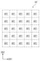
도 5는 도 4a의 AA` 영역을 확대하여 도시한 평면도이다. 도 4a는 도 5의 제1 표시 영역(DA1)의 일부 영역을 확대하여 도시한 것이다.Fig. 5 is a plan view illustrating an enlarged view of area AA` of Fig. 4a. Fig. 4a is an enlarged view illustrating a portion of the first display area (DA1) of Fig. 5.
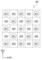
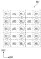
도 4a 및 도 5를 참조하면, 제1 표시 영역(DA1)은 복수의 서브 영역들(AR1)로 구분될 수 있다. 복수의 서브 영역들(AR1) 각각에는 적어도 하나의 화소가 배치될 수 있다. 복수의 서브 영역들(AR1)은 제1 방향(DR1) 및 제2 방향(DR2) 각각을 따라 배열될 수 있다.Referring to FIGS. 4A and 5, the first display area (DA1) may be divided into a plurality of sub-areas (AR1). At least one pixel may be arranged in each of the plurality of sub-areas (AR1). The plurality of sub-areas (AR1) may be arranged along each of the first direction (DR1) and the second direction (DR2).
도 6a 내지 도 6g의 도 4a의 BB` 영역을 확대하여 도시한 평면도들이다. 도 6a 내지 도 6g는 도 5의 제2 표시 영역(DA2)의 일부 영역을 확대하여 도시한 것이다.Figures 6a to 6g are enlarged plan views illustrating the BB` area of Figure 4a. Figures 6a to 6g are enlarged views illustrating a portion of the second display area (DA2) of Figure 5.
제2 표시 영역(DA2)은 제1 서브 영역(AR1) 및 제2 서브 영역(AR2)을 포함할 수 있다. 제1 서브 영역(AR1)은 도 5의 서브 영역들(AR1) 중 하나와 실질적으로 동일할 수 있다. 도 6a 내지 도 6g에서는 구분의 편의를 위해, 제1 서브 영역(AR1) 주변에 원을 표시하였다.The second display area (DA2) may include a first sub-area (AR1) and a second sub-area (AR2). The first sub-area (AR1) may be substantially identical to one of the sub-areas (AR1) of FIG. 5. In FIGS. 6A to 6G, a circle is drawn around the first sub-area (AR1) for convenience of distinction.
제1 서브 영역(AR1)의 제1 반사율은 제2 서브 영역(AR2)의 제2 반사율보다 높을 수 있다. 즉, 제2 서브 영역(AR2)에 의해 제2 표시 영역(DA2)의 반사율은 감소될 수 있다.The first reflectivity of the first sub-area (AR1) may be higher than the second reflectivity of the second sub-area (AR2). That is, the reflectivity of the second display area (DA2) may be reduced by the second sub-area (AR2).
제1 서브 영역(AR1)에는 적어도 하나의 화소가 배치되고, 제2 서브 영역(AR2)에는 적어도 하나의 결여 화소가 배치될 수 있다. 상기 결여 화소는 상기 화소를 구성하는 구성 중 일부가 생략된 화소일 수 있다. 상기 결여 화소는 광을 제공하지 못할 수 있다. 즉, 제2 서브 영역(AR2)은 화소를 포함하지 않는 영역일 수 있다. 상기 화소가 영상을 제공할 때, 상기 결여 화소는 영상을 제공하지 못할 수 있다. 제2 서브 영역(AR2)은 저반사 영역, 투과 영역, 비표시 영역, 비발광 영역, 또는 반투과 영역 등으로 지칭될 수 있다. 제2 표시 영역(DA2)은 영상을 제공하지 못하는 제2 서브 영역(AR2)을 포함하기 때문에 제1 표시 영역(DA1)에 비해 해상도가 낮을 수 있다.At least one pixel may be arranged in the first sub-area (AR1), and at least one missing pixel may be arranged in the second sub-area (AR2). The missing pixel may be a pixel in which some of the components constituting the pixel are omitted. The missing pixel may not be able to provide light. That is, the second sub-area (AR2) may be an area that does not include a pixel. When the pixel provides an image, the missing pixel may not be able to provide the image. The second sub-area (AR2) may be referred to as a low-reflective area, a transparent area, a non-display area, a non-light-emitting area, or a semi-transparent area. Since the second display area (DA2) includes the second sub-area (AR2) that does not provide an image, the resolution may be lower than that of the first display area (DA1).
제1 서브 영역(AR1)의 복수의 제1 서브 영역들(AR1, 이하 제1 서브 영역들) 중 하나이고, 제2 서브 영역(AR2)은 복수의 제2 서브 영역들(AR2, 이하 제2 서브 영역들) 중 하나일 수 있다. 제1 서브 영역들(AR1)과 제2 서브 영역들(AR2)은 소정의 규칙을 가지고 배열될 수 있다.The first sub-region (AR1) may be one of a plurality of first sub-regions (AR1, hereinafter referred to as first sub-regions), and the second sub-region (AR2) may be one of a plurality of second sub-regions (AR2, hereinafter referred to as second sub-regions). The first sub-regions (AR1) and the second sub-regions (AR2) may be arranged according to a predetermined rule.
도 6a 내지 도 6g에서는 제1 서브 영역들(AR1)과 제2 서브 영역들(AR2)의 배열 관계를 예시적으로 도시하였다. 하지만, 본 발명이 이에 제한되는 것은 아니다. 제2 표시 영역(DA2)이 제1 서브 영역들(AR1)과 제2 서브 영역들(AR2)을 모두 포함하는 구조라면 다양하게 변형될 수 있을 것이다.In FIGS. 6A to 6G, the arrangement relationship between the first sub-areas (AR1) and the second sub-areas (AR2) is exemplarily illustrated. However, the present invention is not limited thereto. If the second display area (DA2) has a structure that includes both the first sub-areas (AR1) and the second sub-areas (AR2), it may be modified in various ways.
도 6a를 참조하면, 제1 서브 영역들(AR1) 및 제2 서브 영역들(AR2)은 제1 방향(DR1) 및 제2 방향(DR2)으로 교대로 번갈아 배열될 수 있다. 예를 들어, 하나의 제1 서브 영역(AR1)과 하나의 제2 서브 영역(AR2)이 번갈아 배열될 수 있다.Referring to FIG. 6a, the first sub-regions (AR1) and the second sub-regions (AR2) may be arranged alternately in the first direction (DR1) and the second direction (DR2). For example, one first sub-region (AR1) and one second sub-region (AR2) may be arranged alternately.
도 6b는 도 6a와 비교하였을 때, 동일한 면적 내에서 제2 서브 영역들(AR2)의 수가 더 많기 때문에, 도 6a보다 반사율이 더 낮을 수 있다.Fig. 6b may have a lower reflectivity than Fig. 6a because the number of second sub-regions (AR2) is greater within the same area compared to Fig. 6a.
도 6b를 참조하면, 제1 서브 영역들(AR1) 각각은 제2 서브 영역들(AR2)에 의해 에워싸일 수 있다. 예를 들어, 제1 행과 제2 행이 제2 방향(DR2)을 따라 번갈아 가며 배열될 수 있다. 상기 제1 행은 하나의 제1 서브 영역(AR1)과 하나의 제2 서브 영역(AR2)이 제1 방향(DR1)을 따라 배열된 행일 수 있다. 상기 제2 행은 제2 서브 영역들(AR2)이 제1 방향(DR1)을 따라 배열된 행일 수 있다.Referring to FIG. 6B, each of the first sub-regions (AR1) may be surrounded by second sub-regions (AR2). For example, the first row and the second row may be arranged alternately along the second direction (DR2). The first row may be a row in which one first sub-region (AR1) and one second sub-region (AR2) are arranged along the first direction (DR1). The second row may be a row in which the second sub-regions (AR2) are arranged along the first direction (DR1).
도 6c를 참조하면, 제1 서브 영역들(AR1) 각각은 제2 서브 영역들(AR2)에 의해 에워싸일 수 있다. 예를 들어, 제1 열, 제2 열, 제3 열, 및 제2 열이 제1 방향(DR1)을 따라 번갈아 가며 배열될 수 있다. 상기 제1 열은 하나의 제1 서브 영역(AR1)과 하나의 제2 서브 영역(AR2)이 제2 방향(DR2)을 따라 배열된 열일 수 있다. 상기 제2 열은 제2 서브 영역들(AR2)이 제2 방향(DR2)을 따라 배열된 열일 수 있다. 상기 제3 열은 하나의 제1 서브 영역(AR1)과 하나의 제2 서브 영역(AR2)이 제2 방향(DR2)을 따라 교대로 배열된 열일 수 있다. 상기 제1 열의 짝수 번째 행이 제2 서브 영역(AR2)인 경우, 상기 제3 열의 짝수 번째 행은 제1 서브 영역(AR1)일 수 있다.Referring to FIG. 6c, each of the first sub-regions (AR1) may be surrounded by second sub-regions (AR2). For example, a first column, a second column, a third column, and a second column may be arranged alternately along the first direction (DR1). The first column may be a column in which one first sub-region (AR1) and one second sub-region (AR2) are arranged along the second direction (DR2). The second column may be a column in which the second sub-regions (AR2) are arranged along the second direction (DR2). The third column may be a column in which one first sub-region (AR1) and one second sub-region (AR2) are arranged alternately along the second direction (DR2). When an even-numbered row of the first column is a second sub-region (AR2), an even-numbered row of the third column may be a first sub-region (AR1).
도 6d를 참조하면, 제1 열 및 제2 열이 제1 방향(DR1)을 따라 번갈아 가며 배열될 수 있다. 상기 제1 열은 제1 서브 영역들(AR1)이 제2 방향(DR2)을 따라 배열된 열일 수 있다. 상기 제2 열은 제2 서브 영역들(AR2)이 제2 방향(DR2)을 따라 배열된 열일 수 있다.Referring to FIG. 6d, the first column and the second column may be arranged alternately along the first direction (DR1). The first column may be a column in which the first sub-regions (AR1) are arranged along the second direction (DR2). The second column may be a column in which the second sub-regions (AR2) are arranged along the second direction (DR2).
도 6e를 참조하면, 제1 열, 제2 열, 및 제3 열이 제1 방향(DR1)을 따라 번갈아 가며 배열될 수 있다. 상기 제1 열 및 상기 제2 열 각각은 하나의 제1 서브 영역(AR1)과 하나의 제2 서브 영역(AR2)이 제2 방향(DR2)을 따라 배열된 열일 수 있다. 상기 제3 열은 제2 서브 영역들(AR2)이 제2 방향(DR2)을 따라 배열된 열일 수 있다. 상기 제1 열의 짝수 번째 행이 제2 서브 영역(AR2)인 경우, 상기 제2 열의 짝수 번째 행은 제1 서브 영역(AR1)일 수 있다.Referring to FIG. 6e, a first column, a second column, and a third column may be arranged alternately along a first direction (DR1). Each of the first column and the second column may be a column in which one first sub-region (AR1) and one second sub-region (AR2) are arranged along the second direction (DR2). The third column may be a column in which second sub-regions (AR2) are arranged along the second direction (DR2). When an even-numbered row of the first column is a second sub-region (AR2), an even-numbered row of the second column may be a first sub-region (AR1).
도 6f를 참조하면, 2 개의 제1 행들과 제2 행이 제2 방향(DR2)을 따라 번갈아 가며 배열될 수 있다. 상기 제1 행들 각각은 하나의 제1 서브 영역(AR1)과 하나의 제2 서브 영역(AR2)이 제1 방향(DR1)을 따라 배열된 행일 수 있다. 상기 제2 행은 제2 서브 영역들(AR2)이 제1 방향(DR1)을 따라 배열된 행일 수 있다.Referring to FIG. 6f, two first rows and a second row may be arranged alternately along the second direction (DR2). Each of the first rows may be a row in which one first sub-region (AR1) and one second sub-region (AR2) are arranged along the first direction (DR1). The second row may be a row in which the second sub-regions (AR2) are arranged along the first direction (DR1).
도 6g를 참조하면, 2 개의 제1 열들과 제2 열이 제1 방향(DR1)을 따라 번갈아 가며 배열될 수 있다. 상기 제1 열들 각각은 하나의 제1 서브 영역(AR1)과 하나의 제2 서브 영역(AR2)이 제2 방향(DR2)을 따라 배열된 열일 수 있다. 상기 제2 열은 제2 서브 영역들(AR2)이 제2 방향(DR2)을 따라 배열된 열일 수 있다.Referring to FIG. 6g, two first columns and a second column may be arranged alternately along the first direction (DR1). Each of the first columns may be a column in which one first sub-region (AR1) and one second sub-region (AR2) are arranged along the second direction (DR2). The second column may be a column in which second sub-regions (AR2) are arranged along the second direction (DR2).
도 7a 내지 도 7f는 도 5의 일부 영역을 확대하여 도시한 평면도이다.Figures 7a to 7f are enlarged plan views of some areas of Figure 5.
도 7a 내지 도 7g는 제1 서브 영역(AR1) 내에 배치된 화소 영역들을 도시한 평면도들이다. 제1 서브 영역(AR1)은 적어도 하나의 화소가 배치될 수 있다. 상기 화소에는 화소 영역이 정의될 수 있다. 상기 화소 영역은 소정의 광을 제공하는 영역으로, 후술할 화소 정의막(PDL, 도 8 참조)에 의해 정의된 영역일 수 있다.FIGS. 7A to 7G are plan views illustrating pixel areas arranged within a first sub-area (AR1). At least one pixel may be arranged in the first sub-area (AR1). A pixel area may be defined in the pixel. The pixel area may be an area that provides a predetermined light and may be an area defined by a pixel definition film (PDL, see FIG. 8) to be described later.
도 7a를 참조하면, 제1 서브 영역(AR1)은 제1 화소 영역(PXA1), 제2 화소 영역(PXA2), 및 제3 화소 영역(PXA3)을 포함할 수 있다.Referring to FIG. 7a, the first sub-area (AR1) may include a first pixel area (PXA1), a second pixel area (PXA2), and a third pixel area (PXA3).
복수 개의 화소들(PX, 도 4a 참조)은 레드광을 생성하는 레드 화소, 그린광을 생성하는 그린 화소, 및 블루광을 생성하는 블루 화소를 포함할 수 있다. 본 실시예에서 제1 화소 영역(PXA1)은 레드 화소, 제2 화소 영역(PXA2)은 그린 화소, 및 제3 화소 영역(PXA3)은 블루 화소에 대응할 수 있다.A plurality of pixels (PX, see FIG. 4a) may include a red pixel that generates red light, a green pixel that generates green light, and a blue pixel that generates blue light. In the present embodiment, a first pixel area (PXA1) may correspond to a red pixel, a second pixel area (PXA2) may correspond to a green pixel, and a third pixel area (PXA3) may correspond to a blue pixel.
제1 화소 영역(PXA1), 제2 화소 영역(PXA2), 및 제3 화소 영역(PXA3)은 소정의 방향을 일렬로 배열될 수 있다. 제1 화소 영역(PXA1), 제2 화소 영역(PXA2), 및 제3 화소 영역(PXA3)의 면적은 서로 동일할 수도 있으며, 서로 상이할 수도 있다.The first pixel area (PXA1), the second pixel area (PXA2), and the third pixel area (PXA3) can be arranged in a row in a predetermined direction. The areas of the first pixel area (PXA1), the second pixel area (PXA2), and the third pixel area (PXA3) may be the same as each other or may be different from each other.
도 7b를 참조하면, 제1 서브 영역(AR1)은 제1 화소 영역(PXA1), 제2 화소 영역(PXA2), 및 제3 화소 영역(PXA3)을 포함할 수 있다. 제1 화소 영역(PXA1), 제2 화소 영역(PXA2), 및 제3 화소 영역(PXA3) 각각은 직사각 형상을 가질 수 있다. 제1 화소 영역(PXA1) 및 제2 화소 영역(PXA2)은 가로 방향으로 길게 정의되고, 제3 화소 영역(PXA3)은 세로 방향으로 길게 정의될 수 있다.Referring to FIG. 7b, the first sub-area (AR1) may include a first pixel area (PXA1), a second pixel area (PXA2), and a third pixel area (PXA3). Each of the first pixel area (PXA1), the second pixel area (PXA2), and the third pixel area (PXA3) may have a rectangular shape. The first pixel area (PXA1) and the second pixel area (PXA2) may be defined to be long in the horizontal direction, and the third pixel area (PXA3) may be defined to be long in the vertical direction.
도 7a 및 도 7b 각각에서는 하나의 제1 서브 영역(AR1)이 3 개의 화소 영역들을 포함한 것을 예로 들어 도시하였으나, 본 발명이 이에 제한되는 것은 아니다. 예를 들어, 하나의 제1 서브 영역(AR1)은 하나의 화소 영역, 두 개의 화소 영역들, 또는 4 개 이상의 화소 영역들을 포함할 수도 있다.In each of FIGS. 7A and 7B, one first sub-area (AR1) includes three pixel areas as an example, but the present invention is not limited thereto. For example, one first sub-area (AR1) may include one pixel area, two pixel areas, or four or more pixel areas.
도 7c를 참조하면, 제1 서브 영역(AR1)은 제1 화소 영역(PXA1p), 제2 화소 영역(PXA2p), 및 제3 화소 영역(PXA3p)을 포함할 수 있다. 제1 화소 영역(PXA1p), 제2 화소 영역(PXA2p), 및 제3 화소 영역(PXA3p) 각각은 마름모 형상을 가질 수 있다. 제1 화소 영역(PXA1p), 제2 화소 영역(PXA2p), 및 제3 화소 영역(PXA3p)은 서로 다른 면적을 가질 수 있다. 제1 화소 영역(PXA1p)은 제1 면적을 갖고, 제2 화소 영역(PXA2p)은 제2 면적을 갖고, 및 제3 화소 영역(PXA3p)은 제3 면적을 가질 수 있다. 상기 제1 면적은 상기 제1 면적보다 크고, 상기 제3 면적은 상기 제2 면적보다 클 수 있다. 도 7c와 같은 배열 형태는 펜타일 형태로 지칭될 수 있다.Referring to FIG. 7c, the first sub-region (AR1) may include a first pixel region (PXA1p), a second pixel region (PXA2p), and a third pixel region (PXA3p). Each of the first pixel region (PXA1p), the second pixel region (PXA2p), and the third pixel region (PXA3p) may have a rhombus shape. The first pixel region (PXA1p), the second pixel region (PXA2p), and the third pixel region (PXA3p) may have different areas. The first pixel region (PXA1p) may have a first area, the second pixel region (PXA2p) may have a second area, and the third pixel region (PXA3p) may have a third area. The first area may be larger than the first area, and the third area may be larger than the second area. An arrangement form such as FIG. 7c may be referred to as a pentile form.
도 7d를 참조하면, 제1 서브 영역(AR1)은 도 7c와 비교하였을 때 제3 화소 영역(PXA3p)을 하나 더 포함할 수 있다.Referring to FIG. 7d, the first sub-area (AR1) may include one more third pixel area (PXA3p) compared to FIG. 7c.
도 7e를 참조하면, 제1 서브 영역(AR1)은 제3 화소 영역(PXA3p)을 포함하지 않을 수 있다.Referring to FIG. 7e, the first sub-area (AR1) may not include the third pixel area (PXA3p).
도 7f를 참조하면, 제1 서브 영역(AR1)은 제1 화소 영역(PXA1p)을 포함하지 않을 수 있다.Referring to FIG. 7f, the first sub-area (AR1) may not include the first pixel area (PXA1p).
도 8은 본 발명의 일 실시예에 따른 표시 패널의 일부를 도시한 단면도이다. 도 8은 표시 패널(DP, 도 4a 참조)의 하나의 화소가 배치된 영역을 절단한 단면도이다. 도 8에 도시된 영역은 제1 서브 영역(AR1)일 수 있다. 제1 서브 영역(AR1)은 제1 표시 영역(DA1)에 포함된 영역일 수도 있고, 제2 표시 영역(DA2)에 포함된 영역일 수도 있다.FIG. 8 is a cross-sectional view illustrating a portion of a display panel according to one embodiment of the present invention. FIG. 8 is a cross-sectional view of an area in which one pixel of the display panel (DP, see FIG. 4a) is arranged. The area illustrated in FIG. 8 may be a first sub-area (AR1). The first sub-area (AR1) may be an area included in the first display area (DA1) or an area included in the second display area (DA2).
도 4a 및 도 8을 참조하면, 화소들(PX) 각각은 발광 소자(OLED) 및 화소 회로를 포함할 수 있다. 화소 회로는 복수의 트랜지스터들(TR), 신호 라인들(GL, DL, PL, ECL), 및 커패시터를 포함할 수 있다. 도 8에서는 하나의 트랜지스터(TR)에 대해서만 도시되었다. 화소들(PX) 각각에는 화소 영역이 정의될 수 있고, 도 8 에서는 하나의 화소 영역(PXA1p)이 도시되었다. 제1 서브 영역(AR1)은 화소 영역(PXA1p) 및 비발광 영역(NPXA)을 포함할 수 있다. 비발광 영역(NPXA)은 화소 영역(PXA1p)을 에워쌀 수 있다.Referring to FIGS. 4A and 8, each of the pixels (PX) may include a light-emitting element (OLED) and a pixel circuit. The pixel circuit may include a plurality of transistors (TR), signal lines (GL, DL, PL, ECL), and a capacitor. In FIG. 8, only one transistor (TR) is illustrated. A pixel area may be defined for each of the pixels (PX), and in FIG. 8, one pixel area (PXA1p) is illustrated. The first sub-area (AR1) may include a pixel area (PXA1p) and a non-light-emitting area (NPXA). The non-light-emitting area (NPXA) may surround the pixel area (PXA1p).
표시 패널(DP)은 베이스층(BL), 회로층(ML), 발광 소자층(EL), 및 봉지층(TFE)을 포함할 수 있다. 회로층(ML)은 트랜지스터(TR) 및 복수의 절연층들(BFL, L1, L2, L3, L4)을 포함할 수 있다.The display panel (DP) may include a base layer (BL), a circuit layer (ML), a light emitting element layer (EL), and an encapsulation layer (TFE). The circuit layer (ML) may include a transistor (TR) and a plurality of insulating layers (BFL, L1, L2, L3, L4).
베이스층(BL) 위에는 절연층(BFL)이 배치되고, 절연층(BFL) 위에는 트랜지스터(TR)가 배치될 수 있다. 트랜지스터(TR)는 반도체층(ACL), 제어 전극(GED), 제1 전극(ED1) 및 제2 전극(ED2)을 포함할 수 있다.An insulating layer (BFL) may be arranged on the base layer (BL), and a transistor (TR) may be arranged on the insulating layer (BFL). The transistor (TR) may include a semiconductor layer (ACL), a control electrode (GED), a first electrode (ED1), and a second electrode (ED2).
반도체층(ACL)은 절연층(BFL) 위에 배치될 수 있다. 절연층(BFL)은 반도체층(ACL)에 개질된 표면을 제공하는 버퍼층일 수 있다. 이 경우, 반도체층(ACL)은 베이스층(BL)보다 절연층(BFL)에 대해 높은 접착력을 가질 수 있다. 또한, 절연층(BFL)은 반도체층(ACL)의 하면을 보호하는 배리어층일 수 있다. 이 경우, 절연층(BFL)은 베이스층(BL) 자체 또는 베이스층(BL)을 통해 유입되는 오염이나 습기 등이 반도체층(ACL)으로 침투되는 것을 차단할 수 있다. 또는, 절연층(BFL)은 베이스층(BL)을 통해 입사되는 외부 광이 반도체층(ACL)으로 입사되는 것을 차단하는 광 차단층일 수 있다. 이 경우, 절연층(BFL)은 차광 물질을 더 포함할 수 있다.The semiconductor layer (ACL) may be arranged on the insulating layer (BFL). The insulating layer (BFL) may be a buffer layer that provides a modified surface to the semiconductor layer (ACL). In this case, the semiconductor layer (ACL) may have higher adhesion to the insulating layer (BFL) than to the base layer (BL). In addition, the insulating layer (BFL) may be a barrier layer that protects a lower surface of the semiconductor layer (ACL). In this case, the insulating layer (BFL) may block contamination or moisture, etc., introduced through the base layer (BL) itself or the base layer (BL) from penetrating into the semiconductor layer (ACL). Alternatively, the insulating layer (BFL) may be a light-blocking layer that blocks external light incident through the base layer (BL) from entering the semiconductor layer (ACL). In this case, the insulating layer (BFL) may further include a light-blocking material.
반도체층(ACL)은 폴리 실리콘 또는 아몰포스 실리콘을 포함할 수 있다. 그밖에 반도체층(ACL)은 금속 산화물 반도체를 포함할 수 있다. 반도체층(ACL)은 전자 또는 정공이 이동할 수 있는 통로역할을 하는 채널영역, 채널영역을 사이에 두고 배치된 제1 이온도핑영역 및 제2 이온도핑영역을 포함할 수 있다.The semiconductor layer (ACL) may include polysilicon or amorphous silicon. In addition, the semiconductor layer (ACL) may include a metal oxide semiconductor. The semiconductor layer (ACL) may include a channel region that acts as a passage through which electrons or holes can move, a first ion doping region and a second ion doping region arranged with the channel region interposed therebetween.
제1 절연층(L1)은 절연층(BFL) 위에 배치되며, 반도체층(ACL)을 커버할 수 있다. 제1 절연층(L1)은 무기 물질을 포함할 수 있다. 상기 무기 물질은 실리콘 나이트라이드, 실리콘 옥시 나이트라이드, 실리콘 옥사이드, 티타늄옥사이드 및 알루미늄옥사이드 중 적어도 어느 하나를 포함할 수 있다.The first insulating layer (L1) is disposed on the insulating layer (BFL) and can cover the semiconductor layer (ACL). The first insulating layer (L1) can include an inorganic material. The inorganic material can include at least one of silicon nitride, silicon oxynitride, silicon oxide, titanium oxide, and aluminum oxide.
제1 절연층(L1) 위에는 제어 전극(GED)이 배치될 수 있다. 제2 절연층(L2)은 제1 절연층(L1) 위에 배치되며, 제어 전극(GED)을 커버할 수 있다. 제2 절연층(L2)은 무기 물질을 포함할 수 있다.A control electrode (GED) may be arranged on the first insulating layer (L1). A second insulating layer (L2) may be arranged on the first insulating layer (L1) and may cover the control electrode (GED). The second insulating layer (L2) may include an inorganic material.
제2 절연층(L2) 위에는 제3 절연층(L3)이 배치될 수 있다. 제3 절연층(L3) 위에는 제1 전극(ED1) 및 제2 전극(ED2)이 배치될 수 있다. 제1 전극(ED1) 및 제2 전극(ED2)은 제1 절연층(L1), 제2 절연층(L2) 및 제3 절연층(L3)을 관통하는 관통홀들을 통해 반도체층(ACL)과 연결될 수 있다.A third insulating layer (L3) may be arranged on the second insulating layer (L2). A first electrode (ED1) and a second electrode (ED2) may be arranged on the third insulating layer (L3). The first electrode (ED1) and the second electrode (ED2) may be connected to the semiconductor layer (ACL) through through holes that penetrate the first insulating layer (L1), the second insulating layer (L2), and the third insulating layer (L3).
제4 절연층(L4)은 제3 절연층(L3) 위에 배치되며, 제1 전극(ED1) 및 제2 전극(ED2)를 커버할 수 있다. 제4 절연층(L4)은 단일층 또는 복수의 층으로 구성될 수 있다. 예를 들어, 상기 단일층은 유기층을 포함할 수 있다. 상기 복수의 층은 유기층 및 무기층이 적층되어 제공될 수 있다. 제4 절연층(L4)은 상부에 평탄면을 제공하는 평탄화층일 수 있다.The fourth insulating layer (L4) is disposed on the third insulating layer (L3) and can cover the first electrode (ED1) and the second electrode (ED2). The fourth insulating layer (L4) can be composed of a single layer or multiple layers. For example, the single layer can include an organic layer. The multiple layers can be provided by stacking organic layers and inorganic layers. The fourth insulating layer (L4) can be a planarizing layer that provides a flat surface thereon.
제4 절연층(L4) 위에는 발광 소자층(EL) 및 화소 정의막(PDL)이 배치될 수 있다.A light emitting element layer (EL) and a pixel defining layer (PDL) can be placed on the fourth insulating layer (L4).
발광 소자층(EL)은 발광 소자(OLED) 및 화소 정의막(PDL)을 포함할 수 있다. 발광 소자(OLED)는 제1 전극(E1), 발광층(EM), 및 제2 전극(E2)을 포함할 수 있다. 제1 전극(E1)은 제4 절연층(L4) 위에 배치되고, 제4 절연층(L4)에 정의된 관통홀을 통해 제2 전극(ED2)에 전기적으로 연결될 수 있다. 발광 소자층(EL)은 도 4a에서 설명된 발광 소자(OLED)에 대응될 수 있다.The light emitting element layer (EL) may include a light emitting element (OLED) and a pixel defining layer (PDL). The light emitting element (OLED) may include a first electrode (E1), an emitting layer (EM), and a second electrode (E2). The first electrode (E1) may be disposed on a fourth insulating layer (L4) and may be electrically connected to the second electrode (ED2) through a through hole defined in the fourth insulating layer (L4). The light emitting element layer (EL) may correspond to the light emitting element (OLED) described in FIG. 4A.
화소 정의막(PDL)은 회로층(ML) 위에 배치되어 화소 영역(PXA1p)을 정의할 수 있다. 화소 정의막(PDL)은 제1 전극(E1)의 적어도 일부를 커버하며 제4 절연층(L4) 위에 배치될 수 있다. 제1 전극(E1)의 일부분은 화소 정의막(PDL)에 의해 커버되지 않을 수 있고, 상기 일부분은 화소 영역(PXA1p)에 대응될 수 있다.A pixel defining layer (PDL) can be arranged on a circuit layer (ML) to define a pixel area (PXA1p). The pixel defining layer (PDL) covers at least a portion of a first electrode (E1) and can be arranged on a fourth insulating layer (L4). A portion of the first electrode (E1) may not be covered by the pixel defining layer (PDL), and the portion may correspond to the pixel area (PXA1p).
발광층(EM)은 제1 전극(E1) 및 제2 전극(E2) 사이에 배치될 수 있다. 발광층(EM)은 단일 물질로 이루어진 단일층 구조, 복수의 서로 다른 물질로 이루어진 단일층 구조, 또는 복수의 서로 다른 물질로 이루어진 복수의 층으로 구성된 다층 구조를 가질 수 있다.The light-emitting layer (EM) can be disposed between the first electrode (E1) and the second electrode (E2). The light-emitting layer (EM) can have a single-layer structure composed of a single material, a single-layer structure composed of a plurality of different materials, or a multi-layer structure composed of a plurality of layers composed of a plurality of different materials.
발광층(EM)은 유기물을 포함할 수 있다. 유기물은 통상적으로 사용하는 물질이라면 특별히 한정되지 않는다. 예를 들어, 발광층(EM)은 적색, 녹색, 또는 청색을 발광하는 물질들 중 적어도 어느 하나의 물질로 구성될 수 있으며, 형광 물질 또는 인광 물질을 포함할 수 있다.The emitting layer (EM) may include an organic material. The organic material is not particularly limited as long as it is a commonly used material. For example, the emitting layer (EM) may be composed of at least one material that emits red, green, or blue light, and may include a fluorescent material or a phosphorescent material.
제2 전극(E2)은 발광층(EM) 및 화소 정의막(PDL) 위에 배치될 수 있다. 제2 전극(E2)은 제2 전원을 수신할 수 있다.The second electrode (E2) can be disposed on the light-emitting layer (EM) and the pixel defining layer (PDL). The second electrode (E2) can receive a second power source.
제2 전극(E2) 위에는 봉지층(TFE)이 배치된다. 봉지층(TFE)은 제2 전극(E2)을 직접 커버할 수 있다. 본 발명의 다른 실시예에서는, 봉지층(TFE)과 제2 전극(E2) 사이에 제2 전극(E2)을 커버하는 캡핑층이 더 배치될 수 있다. 이 경우, 봉지층(TFE)은 캡핑층을 직접 커버할 수 있다. 캡핑층은 유기물을 포함할 수 있다. 캡핑층은 후속의 공정 예컨대 스퍼터링 공정으로부터 제2 전극(E2)을 보호하고, 발광 소자층(EL)의 출광효율을 향상시킬 수 있다.A sealing layer (TFE) is disposed on the second electrode (E2). The sealing layer (TFE) can directly cover the second electrode (E2). In another embodiment of the present invention, a capping layer covering the second electrode (E2) can be further disposed between the sealing layer (TFE) and the second electrode (E2). In this case, the sealing layer (TFE) can directly cover the capping layer. The capping layer can include an organic material. The capping layer can protect the second electrode (E2) from a subsequent process, such as a sputtering process, and can improve the light emission efficiency of the light-emitting element layer (EL).
봉지층(TFE)은 유기층 및 무기층을 포함할 수 있으며, 무기층은 수분 및 산소로부터 발광 소자(OLED)를 보호할 수 있고, 유기층은 먼지 입자와 같은 이물질로부터 발광 소자(OLED)를 보호할 수 있다.The encapsulating layer (TFE) may include an organic layer and an inorganic layer, wherein the inorganic layer may protect the light-emitting element (OLED) from moisture and oxygen, and the organic layer may protect the light-emitting element (OLED) from foreign substances such as dust particles.
도 9는 도 6a의 일부 영역을 확대하여 도시한 평면도이다.Figure 9 is a plan view showing an enlarged portion of a part of Figure 6a.
도 9는 제2 서브 영역(AR2)의 결여 화소 영역을 도시한 평면도이다. 결여 화소는 영상을 제공하지 않는 영역이다. 설명의 편의를 위해, 화소 영역과 대응하는 결여 화소 영역을 점선으로 도시하였다.Figure 9 is a plan view illustrating a missing pixel area of the second sub-area (AR2). A missing pixel is an area that does not provide an image. For convenience of explanation, a missing pixel area corresponding to a pixel area is illustrated with a dotted line.
예를 들어, 제2 서브 영역(AR2)은 제1 결여 화소 영역(IPXA1p) 및 제2 결여 화소 영역(IPXA2p)을 포함할 수 있다. 이는 도 7e에 도시된 제1 서브 영역(AR1)의 제1 화소 영역(PXA1p) 및 제2 화소 영역(PXA2p)에 대응될 수 있다.For example, the second sub-region (AR2) may include a first missing pixel region (IPXA1p) and a second missing pixel region (IPXA2p). This may correspond to the first pixel region (PXA1p) and the second pixel region (PXA2p) of the first sub-region (AR1) illustrated in FIG. 7e.
도 5를 참조하면, 제1 표시 영역(DR1)은 복수의 제1 서브 영역들(AR1)을 포함한다. 하나의 제1 서브 영역(AR1)은 도 7f와 같이 제2 화소 영역(PXA2p) 및 제3 화소 영역(PXA3p)을 포함할 수 있다. 상기 하나의 제1 서브 영역(AR1)과 제1 방향(DR1)으로 인접한 다른 하나의 제1 서브 영역(AR1)은 도 7e와 같이 제1 화소 영역(PXA1p) 및 제2 화소 영역(PXA2p)을 포함할 수 있다.Referring to FIG. 5, the first display area (DR1) includes a plurality of first sub-areas (AR1). One first sub-area (AR1) may include a second pixel area (PXA2p) and a third pixel area (PXA3p), as shown in FIG. 7f. Another first sub-area (AR1) adjacent to one first sub-area (AR1) in the first direction (DR1) may include a first pixel area (PXA1p) and a second pixel area (PXA2p), as shown in FIG. 7e.
제2 표시 영역(DR2, 도 4a 참조)은 제1 서브 영역(AR1)과 제2 서브 영역(AR2)을 포함할 수 있다. 제2 서브 영역(AR2)은 결여 화소를 포함하는 영역, 즉, 화소를 포함하지 않는 영역일 수 있다. 즉, 제2 서브 영역(AR2)은 도 7e의 제1 화소 영역(PXA1p) 및 제2 화소 영역(PXA2p)이 결여 화소 영역들로 변경된 영역일 수 있다.The second display area (DR2, see FIG. 4a) may include a first sub-area (AR1) and a second sub-area (AR2). The second sub-area (AR2) may be an area including a missing pixel, that is, an area that does not include a pixel. That is, the second sub-area (AR2) may be an area in which the first pixel area (PXA1p) and the second pixel area (PXA2p) of FIG. 7e are changed into missing pixel areas.
도 10a는 본 발명의 일 실시예에 따른 표시 패널의 일부를 도시한 단면도이다. 도 10b는 본 발명의 일 실시예에 따른 표시 패널의 일부를 도시한 평면도이다. 도 10c는 본 발명의 일 실시예에 따른 표시 패널의 일부를 도시한 평면도이다.FIG. 10A is a cross-sectional view illustrating a portion of a display panel according to one embodiment of the present invention. FIG. 10B is a plan view illustrating a portion of a display panel according to one embodiment of the present invention. FIG. 10C is a plan view illustrating a portion of a display panel according to one embodiment of the present invention.
도 10a에 도시된 영역은 제2 서브 영역(AR2)일 수 있다. 제2 서브 영역(AR2)은 제2 표시 영역(DA2, 도 4a 참조)에 포함된 영역일 수 있다.The area illustrated in Fig. 10a may be a second sub-area (AR2). The second sub-area (AR2) may be an area included in the second display area (DA2, see Fig. 4a).
도 8 및 도 10a를 참조하면, 제2 서브 영역(AR2)에는 결여 화소가 배치될 수 있다. 결여 화소는 화소에서 제1 전극(E1), 발광층(EM), 제2 전극(E2), 및 트랜지스터(TR) 중 적어도 하나가 생략된 화소일 수 있다.Referring to FIG. 8 and FIG. 10a, a missing pixel may be arranged in the second sub-region (AR2). The missing pixel may be a pixel in which at least one of the first electrode (E1), the light-emitting layer (EM), the second electrode (E2), and the transistor (TR) is omitted.
도 10a에서는 도 8의 화소 영역(PXA1p)과 대응하는 결여 화소 영역(IPXA1p)을 표시하였다. 또한, 트랜지스터(TR)가 생략된 제1 영역(CPA1), 제1 전극(E1)이 생략된 제2 영역(CPA2), 및 제2 전극(E2)이 생략된 제3 영역(CPA3)이 도시되었다.In Fig. 10a, a missing pixel area (IPXA1p) corresponding to the pixel area (PXA1p) of Fig. 8 is shown. In addition, a first area (CPA1) in which a transistor (TR) is omitted, a second area (CPA2) in which a first electrode (E1) is omitted, and a third area (CPA3) in which a second electrode (E2) is omitted are shown.
도 10a의 결여 화소는 제1 전극(E1), 발광층(EM), 제2 전극(E2), 및 트랜지스터(TR)가 모두 생략된 화소일 수 있다. 평면 상에서 보았을 때, 결여 화소는 화소에 비해 금속층이 생략된 구조를 가질 수 있다. 따라서, 결여 화소의 반사율은 화소의 반사율보다 낮을 수 있다. 또한, 결여 화소의 투과율은 화소의 투과율보다 높을 수 있다.The missing pixel of Fig. 10a may be a pixel in which the first electrode (E1), the light-emitting layer (EM), the second electrode (E2), and the transistor (TR) are all omitted. When viewed on a plane, the missing pixel may have a structure in which a metal layer is omitted compared to the pixel. Accordingly, the reflectivity of the missing pixel may be lower than the reflectivity of the pixel. In addition, the transmittance of the missing pixel may be higher than the transmittance of the pixel.
도 10b를 참조하면, 제2 서브 영역(AR2)의 평면도를 도시하였다. 제2 서브 영역(AR2)에는 제1 전극(E1), 발광층(EM), 제2 전극(E2), 및 트랜지스터(TR)가 모두 제거될 수 있다. 하지만, 제2 서브 영역(AR2) 주변에 제1 서브 영역(AR1)이 배치되기 때문에, 제1 서브 영역(AR1)으로 신호를 전달할 라인들은 제2 서브 영역(AR2)에 배치될 수 있다. 예를 들어, 제2 서브 영역(AR2)에 신호 라인들은 배치될 수 있다. 도 10b에서는 신호 라인들 중 스캔 라인(GL) 및 데이터 라인(DL)에 대해서만 예시적으로 도시하였다.Referring to FIG. 10b, a plan view of the second sub-region (AR2) is illustrated. In the second sub-region (AR2), the first electrode (E1), the light-emitting layer (EM), the second electrode (E2), and the transistor (TR) can all be removed. However, since the first sub-region (AR1) is arranged around the second sub-region (AR2), lines for transmitting signals to the first sub-region (AR1) can be arranged in the second sub-region (AR2). For example, signal lines can be arranged in the second sub-region (AR2). In FIG. 10b, only the scan line (GL) and the data line (DL) among the signal lines are illustrated as examples.
도 10c를 참조하면, 제1 서브 영역들(AR1), 제2 서브 영역들(AR2), 및 제2 전극(E2)이 도시되었다. 제2 전극(E2)은 액티브 영역(AA, 도 4a 참조) 전체에 배치될 수 있다. 제2 전극(E2)에는 공통 전압이 제공될 수 있다.Referring to FIG. 10c, first sub-regions (AR1), second sub-regions (AR2), and a second electrode (E2) are illustrated. The second electrode (E2) may be arranged over the entire active area (AA, see FIG. 4a). A common voltage may be provided to the second electrode (E2).
제2 전극(E2)의 제2 서브 영역들(AR2)과 중첩하는 영역들에는 개구부들(E2-H)이 제공될 수 있다. 개구부들(E2-H)은 제2 전극(E2)의 일부분이 제거되어 정의될 수 있다.Openings (E2-H) may be provided in areas overlapping the second sub-areas (AR2) of the second electrode (E2). The openings (E2-H) may be defined by removing a portion of the second electrode (E2).
제2 전극(E2)에 개구부들(E2-H)을 형성하는 공정은 다양한 공정이 이용될 수 있다. 예를 들어, 스탬핑 공정을 이용하여 개구부들(E2-H)을 형성하거나, 레이저 드릴링 공정을 이용하여 개구부들(E2-H)을 형성할 수 있다. 또한, 복수의 마스크 공정을 이용하여 개구부들(E2-H)을 포함하는 제2 전극(E2)을 형성할 수도 있다. 개구부들(E2-H)을 형성하는 공정은 상기 예로 제시된 공정 외에 다양한 공정들이 이용될 수 있다.The process of forming the openings (E2-H) in the second electrode (E2) may utilize various processes. For example, the openings (E2-H) may be formed using a stamping process, or the openings (E2-H) may be formed using a laser drilling process. In addition, the second electrode (E2) including the openings (E2-H) may be formed using a plurality of mask processes. The process of forming the openings (E2-H) may utilize various processes in addition to the processes presented as examples above.
도 11은 본 발명의 일 실시예에 따른 표시 패널의 일부를 도시한 단면도이다.FIG. 11 is a cross-sectional view illustrating a portion of a display panel according to one embodiment of the present invention.
도 8 및 도 11을 참조하면, 제2 서브 영역(AR2)에는 결여 화소가 배치될 수 있다. 도 11은 도 8의 화소 영역(PXA1p)과 대응하는 결여 화소 영역(IPXA1p)이 표시되었다. 또한, 트랜지스터(TR)가 생략된 제1 영역(CPA1-1), 및 제1 전극(E1)이 생략된 제2 영역(CPA2-1)이 도시되었다. 도 11에 도시된 결여 화소는 발광층(EM) 및 제2 전극(E2)을 포함할 수 있다. 하지만, 결여 화소는 화소가 발광되기 위한 필수 구성들 중 일부 구성이 생략되었기 때문에, 광을 제공하지 않을 수 있다. 또한, 제1 전극(E1)이 생략되어 투과율이 향상되고, 반사율이 감소될 수 있다.Referring to FIGS. 8 and 11, a missing pixel may be arranged in the second sub-region (AR2). FIG. 11 shows a missing pixel region (IPXA1p) corresponding to the pixel region (PXA1p) of FIG. 8. In addition, a first region (CPA1-1) from which a transistor (TR) is omitted and a second region (CPA2-1) from which a first electrode (E1) is omitted are illustrated. The missing pixel illustrated in FIG. 11 may include an emission layer (EM) and a second electrode (E2). However, the missing pixel may not provide light because some of the essential components for the pixel to emit light are omitted. In addition, since the first electrode (E1) is omitted, transmittance may be improved and reflectance may be reduced.
도 12a는 본 발명의 일 실시예에 따른 표시 패널의 일부를 도시한 단면도이다. 도 12b는 본 발명의 일 실시예에 따른 표시 패널의 일부를 도시한 단면도이다.FIG. 12a is a cross-sectional view illustrating a portion of a display panel according to one embodiment of the present invention. FIG. 12b is a cross-sectional view illustrating a portion of a display panel according to one embodiment of the present invention.
도 12a 및 도 12b를 설명함에 있어서, 도 11에 차이가 있는 부분에 대하여 중점적으로 설명한다. 제2 전극은 제1 전극부(E2) 및 제2 전극부(E2-T)를 포함할 수 있다. 제1 전극부(E2)는 제1 두께를 갖고, 제2 전극부(E2-T)는 제2 두께를 가질 수 있다. 상기 제1 두께는 상기 제2 두께보다 두꺼울 수 있다.In describing FIG. 12a and FIG. 12b, the differences from FIG. 11 will be mainly described. The second electrode may include a first electrode portion (E2) and a second electrode portion (E2-T). The first electrode portion (E2) may have a first thickness, and the second electrode portion (E2-T) may have a second thickness. The first thickness may be thicker than the second thickness.
제1 전극부(E2)는 제1 표시 영역(DA1, 도 4a 참조)에 배치되고, 제2 전극부(E2-T)는 제2 표시 영역(DA2)에 배치될 수 있다.The first electrode part (E2) can be placed in the first display area (DA1, see FIG. 4a), and the second electrode part (E2-T) can be placed in the second display area (DA2).
본 발명의 일 실시예에서, 제2 전극부(E2-T)는 제2 표시 영역(DA2) 전체에 배치될 수 있다. 본 발명의 일 실시예에서, 제2 전극부(E2-T)는 제2 표시 영역(DA2)의 제2 서브 영역(AR2)에만 배치될 수도 있다.In one embodiment of the present invention, the second electrode portion (E2-T) may be arranged in the entire second display area (DA2). In one embodiment of the present invention, the second electrode portion (E2-T) may be arranged only in the second sub-area (AR2) of the second display area (DA2).
제1 전극부(E2)는 복수의 금속층들을 포함할 수 있고, 제2 전극부(E2-T)는 제1 전극부(E2)보다 적은 수의 금속층을 포함할 수도 있다. 예를 들어, 제1 전극부(E2)는 두 개의 금속층들을 포함하고, 제2 전극부(E2-T)는 하나의 금속층을 포함할 수도 있다.The first electrode portion (E2) may include a plurality of metal layers, and the second electrode portion (E2-T) may include a smaller number of metal layers than the first electrode portion (E2). For example, the first electrode portion (E2) may include two metal layers, and the second electrode portion (E2-T) may include one metal layer.
본 발명의 일 실시예에서, 제1 전극부(E2) 및 제2 전극부(E2-T) 각각은 모두 단일 금속층을 포함할 수 있고, 제1 전극부(E2)의 두께와 제2 전극부(E2-T)의 두께가 상이할 수도 있다.In one embodiment of the present invention, each of the first electrode portion (E2) and the second electrode portion (E2-T) may include a single metal layer, and the thickness of the first electrode portion (E2) and the thickness of the second electrode portion (E2-T) may be different.
도 13은 본 발명의 일 실시예에 따른 표시 패널의 일부를 도시한 단면도이다.FIG. 13 is a cross-sectional view illustrating a portion of a display panel according to one embodiment of the present invention.
도 8 및 도 13을 참조하면, 제2 서브 영역(AR2)에는 결여 화소가 배치될 수 있다. 도 13은 도 8의 화소 영역(PXA1p)과 대응하는 결여 화소 영역(IPXA1p)이 표시되었다. 또한, 트랜지스터(TR)가 생략된 제1 영역(CPA1-2), 및 제2 전극(E2)이 생략된 제3 영역(CPA3-2)이 도시되었다. 도 13에 도시된 결여 화소는 발광층(EM) 및 제1 전극(E1)을 포함할 수 있다. 하지만, 결여 화소는 화소가 발광되기 위한 필수 구성들 중 일부 구성이 생략되었기 때문에, 광을 제공하지 않을 수 있다. 또한, 제2 전극(E2)이 생략되어 투과율이 향상되고, 반사율이 감소될 수 있다.Referring to FIGS. 8 and 13, a missing pixel may be arranged in the second sub-region (AR2). FIG. 13 shows a missing pixel region (IPXA1p) corresponding to the pixel region (PXA1p) of FIG. 8. In addition, a first region (CPA1-2) from which a transistor (TR) is omitted, and a third region (CPA3-2) from which a second electrode (E2) is omitted are illustrated. The missing pixel illustrated in FIG. 13 may include an emission layer (EM) and a first electrode (E1). However, since the missing pixel has some of the essential components for the pixel to emit light omitted, it may not provide light. In addition, since the second electrode (E2) is omitted, transmittance may be improved and reflectance may be reduced.
도 14는 본 발명의 일 실시예에 따른 표시 패널의 일부를 도시한 단면도이다.FIG. 14 is a cross-sectional view illustrating a portion of a display panel according to one embodiment of the present invention.
도 8 및 도 14를 참조하면, 제2 서브 영역(AR2)에는 결여 화소가 배치될 수 있다. 도 14에는 도 8의 화소 영역(PXA1p)과 대응하는 결여 화소 영역(IPXA1p)이 표시되었다. 또한, 제1 전극(E1)이 생략된 제2 영역(CPA2-3)이 도시되었다. 도 14에 도시된 결여 화소는 트랜지스터(TR), 발광층(EM) 및 제2 전극(E2)을 포함할 수 있다. 하지만, 결여 화소는 화소가 발광되기 위한 필수 구성들 중 일부 구성이 생략되었기 때문에, 광을 제공하지 않을 수 있다.Referring to FIGS. 8 and 14, a missing pixel may be arranged in the second sub-region (AR2). FIG. 14 illustrates a missing pixel region (IPXA1p) corresponding to the pixel region (PXA1p) of FIG. 8. In addition, a second region (CPA2-3) in which the first electrode (E1) is omitted is illustrated. The missing pixel illustrated in FIG. 14 may include a transistor (TR), an emission layer (EM), and a second electrode (E2). However, the missing pixel may not provide light because some of the essential components for the pixel to emit light are omitted.
도 15는 본 발명의 일 실시예에 따른 표시 패널의 일부를 도시한 단면도이다.FIG. 15 is a cross-sectional view illustrating a portion of a display panel according to one embodiment of the present invention.
도 8 및 도 15를 참조하면, 제2 서브 영역(AR2)에는 결여 화소가 배치될 수 있다. 도 15에는 도 8의 화소 영역(PXA1p)과 대응하는 결여 화소 영역(IPXA1p)이 표시되었다. 또한, 제1 전극(E1)이 생략된 제2 영역(CPA2-4) 및 제2 전극(E2)이 생략된 제3 영역(CPA3-4)이 도시되었다. 도 15에 도시된 결여 화소는 트랜지스터(TR)를 포함할 수 있다. 하지만, 결여 화소는 화소가 발광되기 위한 필수 구성들 중 일부 구성이 생략되었기 때문에, 광을 제공하지 않을 수 있다.Referring to FIGS. 8 and 15, a missing pixel may be arranged in the second sub-region (AR2). FIG. 15 shows a missing pixel region (IPXA1p) corresponding to the pixel region (PXA1p) of FIG. 8. In addition, a second region (CPA2-4) in which the first electrode (E1) is omitted and a third region (CPA3-4) in which the second electrode (E2) is omitted are shown. The missing pixel illustrated in FIG. 15 may include a transistor (TR). However, the missing pixel may not provide light because some of the essential components for the pixel to emit light are omitted.
도 16은 본 발명의 일 실시예에 따른 표시 패널의 일부를 도시한 단면도이다.FIG. 16 is a cross-sectional view illustrating a portion of a display panel according to one embodiment of the present invention.
도 8 및 도 16을 참조하면, 제2 서브 영역(AR2)에는 결여 화소가 배치될 수 있다. 도 16에는 도 8의 화소 영역(PXA1p)과 대응하는 결여 화소 영역(IPXA1p)이 표시되었다. 또한, 제2 전극(E2)이 생략된 제3 영역(CPA3-5)이 도시되었다. 도 16에 도시된 결여 화소는 트랜지스터(TR), 발광층(EM) 및 제1 전극(E1)을 포함할 수 있다. 하지만, 결여 화소는 화소가 발광되기 위한 필수 구성들 중 일부 구성이 생략되었기 때문에, 광을 제공하지 않을 수 있다.Referring to FIGS. 8 and 16, a missing pixel may be arranged in the second sub-region (AR2). FIG. 16 shows a missing pixel region (IPXA1p) corresponding to the pixel region (PXA1p) of FIG. 8. In addition, a third region (CPA3-5) in which the second electrode (E2) is omitted is shown. The missing pixel illustrated in FIG. 16 may include a transistor (TR), an emission layer (EM), and a first electrode (E1). However, the missing pixel may not provide light because some of the essential components for the pixel to emit light are omitted.
도 17a는 본 발명의 일 실시예에 따른 반사 방지 패널의 평면도이다. 도 17b는 본 발명의 일 실시예에 따른 표시 패널의 평면도이다.FIG. 17a is a plan view of an anti-reflection panel according to one embodiment of the present invention. FIG. 17b is a plan view of a display panel according to one embodiment of the present invention.
도 17a를 참조하면, 반사 방지 패널(RPP-1)는 제1 영역(RA1-1) 및 제2 영역(RA2-1)을 포함할 수 있다. 제1 영역(RA1-1)은 제1 투과율을 갖고, 제2 영역(RA2-1)은 상기 제1 투과율보다 높은 제2 투과율을 가질 수 있다. 본 발명의 실시예에 따르면, 전자 모듈(SS, 도 1b 참조)과 중첩하는 영역의 투과율이 향상됨에 따라, 전자 모듈(SS)의 센싱 감도가 보다 향상될 수 있다.Referring to FIG. 17a, the anti-reflection panel (RPP-1) may include a first region (RA1-1) and a second region (RA2-1). The first region (RA1-1) may have a first transmittance, and the second region (RA2-1) may have a second transmittance higher than the first transmittance. According to an embodiment of the present invention, as the transmittance of the region overlapping with the electronic module (SS, see FIG. 1b) is improved, the sensing sensitivity of the electronic module (SS) may be further improved.
제2 영역(RA2-1)의 투과율을 향상시키기 위해, 반사 방지 패널(RPP-1)의 제2 영역(RA2-1)에는 다양한 처리가 적용될 수 있다. 예를 들어, 방사 방지 패널(RPP-1)의 제2 영역(RA2-1)은 탈색되거나, 제거될 수 있다.To improve the transmittance of the second region (RA2-1), various treatments may be applied to the second region (RA2-1) of the anti-reflection panel (RPP-1). For example, the second region (RA2-1) of the anti-reflection panel (RPP-1) may be bleached or removed.
제2 영역(RA2-1)은 반사 방지 패널(RPP-1)의 엣지 영역에 인접하여 정의될 수 있다. 예를 들어, 반사 방지 패널(RPP-1)은 꼭지점들 각각에 곡률을 갖는 사각형상을 가질 수 있다. 제2 영역(RA2-1)은 곡률을 갖는 변 중 적어도 하나를 포함할 수 있다.The second region (RA2-1) may be defined adjacent to an edge region of the anti-reflection panel (RPP-1). For example, the anti-reflection panel (RPP-1) may have a rectangular shape having curvature at each of its vertices. The second region (RA2-1) may include at least one of the sides having a curvature.
제1 영역(RA1-1)은 제2 영역(RA2-1)을 둘러쌀 수 있다. 제1 영역(RA1-1)과 제2 영역(RA2-1)의 경계는 적어도 하나 이상의 변을 포함할 수 있다. 도 17a에서는 상기 경계가 두 개의 변을 포함하는 것을 예시적으로 도시하였다.The first region (RA1-1) can surround the second region (RA2-1). The boundary between the first region (RA1-1) and the second region (RA2-1) can include at least one edge. Fig. 17a illustrates an example in which the boundary includes two edges.
도 17b를 참조하면, 표시 패널(DP-1)에는 제1 표시 영역(DA1-1) 및 제2 표시 영역(DA2-1)이 정의될 수 있다. 제1 표시 영역(DA1-1)은 평면 상에서 제1 영역(RA1-1)과 중첩하는 영역이고, 제2 표시 영역(DA2-1)은 평면 상에서 제2 영역(RA2-1)과 중첩하는 영역일 수 있다.Referring to FIG. 17b, a first display area (DA1-1) and a second display area (DA2-1) may be defined on the display panel (DP-1). The first display area (DA1-1) may be an area overlapping the first area (RA1-1) on a plane, and the second display area (DA2-1) may be an area overlapping the second area (RA2-1) on a plane.
제1 표시 영역(DA1-1)의 해상도보다 제2 표시 영역(DA2-1)의 해상도는 더 낮을 수 있다. 또한, 제1 표시 영역(DA1-1)의 반사율보다 제2 표시 영역(DA2-1)의 반사율은 더 낮을 수 있다.The resolution of the second display area (DA2-1) may be lower than the resolution of the first display area (DA1-1). Additionally, the reflectivity of the second display area (DA2-1) may be lower than the reflectivity of the first display area (DA1-1).
제2 영역(RA2-1)의 외광 반사 방지 성능은 제1 영역(RA1-1)의 외광 반사 방지 성능보다 다소 감소될 수 있다. 하지만, 본 발명의 실시예에 따르면, 제2 영역(RA2-1)에서 외광 반사 방지 성능이 감소되더라도, 제2 표시 영역(DA2-1)의 반사율을 감소시켜 이를 보완할 수 있다. 표시 패널(DP-1)의 제1 표시 영역(DA1-1)과 표시 패널(DP-1)의 제2 표시 영역(DA2-1)에서 해상도 및/또는 반사율을 조절하여 상기 외광 반사 방지 성능을 보완할 수 있다.The external light reflection prevention performance of the second area (RA2-1) may be somewhat reduced compared to the external light reflection prevention performance of the first area (RA1-1). However, according to an embodiment of the present invention, even if the external light reflection prevention performance is reduced in the second area (RA2-1), this can be compensated for by reducing the reflectivity of the second display area (DA2-1). The external light reflection prevention performance can be compensated for by adjusting the resolution and/or reflectivity in the first display area (DA1-1) of the display panel (DP-1) and the second display area (DA2-1) of the display panel (DP-1).
도 18a는 본 발명의 일 실시예에 따른 반사 방지 패널의 평면도이다. 도 18b는 본 발명의 일 실시예에 따른 반사 방지 패널의 평면도이다.FIG. 18a is a plan view of an anti-reflection panel according to one embodiment of the present invention. FIG. 18b is a plan view of an anti-reflection panel according to one embodiment of the present invention.
도 18a를 참조하면, 반사 방지 패널(RPP-2)는 제1 영역(RA1-2) 및 제2 영역(RA2-2)을 포함할 수 있다. 제1 영역(RA1-2)은 제1 투과율을 갖고, 제2 영역(RA2-2)은 상기 제1 투과율보다 높은 제2 투과율을 가질 수 있다. 본 발명의 실시예에 따르면, 전자 모듈(SS, 도 1b 참조)과 중첩하는 영역의 투과율이 향상됨에 따라, 전자 모듈(SS)의 센싱 감도가 보다 향상될 수 있다.Referring to FIG. 18a, the anti-reflection panel (RPP-2) may include a first region (RA1-2) and a second region (RA2-2). The first region (RA1-2) may have a first transmittance, and the second region (RA2-2) may have a second transmittance higher than the first transmittance. According to an embodiment of the present invention, as the transmittance of the region overlapping with the electronic module (SS, see FIG. 1b) is improved, the sensing sensitivity of the electronic module (SS) may be further improved.
제2 영역(RA2-2)은 반사 방지 패널(RPP-2)의 엣지 영역에 인접하여 정의될 수 있다. 예를 들어, 반사 방지 패널(RPP-2)은 꼭지점들 각각에 곡률을 갖는 사각형상을 가질 수 있다. 제2 영역(RA2-2)은 곡률을 갖는 변 중 두 개의 변들을 포함할 수 있다.The second region (RA2-2) may be defined adjacent to an edge region of the anti-reflection panel (RPP-2). For example, the anti-reflection panel (RPP-2) may have a rectangular shape having curvature at each of its vertices. The second region (RA2-2) may include two of the sides having curvature.
도 18b를 참조하면, 표시 패널(DP-2)에는 제1 표시 영역(DA1-2) 및 제2 표시 영역(DA2-2)이 정의될 수 있다. 제1 표시 영역(DA1-2)은 평면 상에서 제1 영역(RA1-2)과 중첩하는 영역이고, 제2 표시 영역(DA2-2)은 평면 상에서 제2 영역(RA2-2)과 중첩하는 영역일 수 있다.Referring to FIG. 18b, a first display area (DA1-2) and a second display area (DA2-2) may be defined on the display panel (DP-2). The first display area (DA1-2) may be an area overlapping the first area (RA1-2) on a plane, and the second display area (DA2-2) may be an area overlapping the second area (RA2-2) on a plane.
제1 표시 영역(DA1-2)의 해상도보다 제2 표시 영역(DA2-2)의 해상도는 더 낮을 수 있다. 또한, 제1 표시 영역(DA1-2)의 반사율보다 제2 표시 영역(DA2-2)의 반사율은 더 낮을 수 있다.The resolution of the second display area (DA2-2) may be lower than the resolution of the first display area (DA1-2). Additionally, the reflectivity of the second display area (DA2-2) may be lower than the reflectivity of the first display area (DA1-2).
이상에서는 본 발명의 바람직한 실시예를 참조하여 설명하였지만, 해당 기술 분야의 숙련된 당업자 또는 해당 기술 분야에 통상의 지식을 갖는 자라면, 후술될 특허청구범위에 기재된 본 발명의 사상 및 기술 영역으로부터 벗어나지 않는 범위 내에서 본 발명을 다양하게 수정 및 변경시킬 수 있음을 이해할 수 있을 것이다. 따라서, 본 발명의 기술적 범위는 명세서의 상세한 설명에 기재된 내용으로 한정되는 것이 아니라 특허청구범위에 의해 정하여져야만 할 것이다.Although the present invention has been described above with reference to preferred embodiments thereof, it will be understood by those skilled in the art or having ordinary knowledge in the art that various modifications and changes may be made to the present invention without departing from the spirit and technical scope of the present invention as set forth in the claims below. Accordingly, the technical scope of the present invention should not be limited to the contents described in the detailed description of the specification, but should be defined by the claims.
EA: 표시 장치 WP: 윈도우
RPP: 반사 방지 패널DM: 표시 모듈
SS: 전자 모듈EA: Display Device WP: Windows
RPP: Anti-reflection panel DM: Display module
SS: Electronic Module
Claims (20)
Translated fromKorean상기 윈도우 아래에 배치되며 제1 투과율을 갖는 제1 영역 및 상기 제1 투과율보다 높은 제2 투과율을 갖는 제2 영역이 정의된 반사 방지 부재; 및
상기 반사 방지 부재 아래에 배치되며, 제1 해상도를 갖는 제1 표시 영역 및 상기 제1 해상도보다 낮은 제2 해상도를 갖는 제2 표시 영역이 정의된 표시 패널을 포함하고, 평면 상에서 상기 제2 영역과 상기 제2 표시 영역은 서로 중첩하고, 상기 제2 표시 영역은 제1 서브 영역 및 제2 서브 영역을 포함하고, 상기 제1 서브 영역의 제1 반사율은 상기 제2 서브 영역의 제2 반사율보다 높은 표시 장치.Windows;
An anti-reflection member positioned below the window and having a first region having a first transmittance and a second region having a second transmittance higher than the first transmittance defined therein; and
A display device comprising a display panel disposed under the anti-reflection member, wherein a first display area having a first resolution and a second display area having a second resolution lower than the first resolution are defined, wherein the second area and the second display area overlap each other on a plane, the second display area includes a first sub-area and a second sub-area, and a first reflectivity of the first sub-area is higher than a second reflectivity of the second sub-area.
상기 표시 패널의 상기 제2 표시 영역 아래에 배치된 전자 모듈을 더 포함하는 표시 장치.In the first paragraph,
A display device further comprising an electronic module disposed below the second display area of the display panel.
상기 반사 방지 부재는 편광자인 표시 장치.In the first paragraph,
The above anti-reflection member is a polarizing display device.
상기 반사 방지 부재의 상기 제2 영역은 탈색된 표시 장치.In the third paragraph,
The second region of the above anti-reflection member is a discolored display device.
상기 반사 방지 부재의 상기 제2 영역에는 홀이 정의된 표시 장치.In the first paragraph,
A display device having a hole defined in the second region of the anti-reflection member.
상기 제1 서브 영역에는 적어도 하나의 화소가 배치되고, 상기 화소는 발광 소자 및 상기 발광 소자와 전기적으로 연결된 화소 회로를 포함하고, 상기 발광 소자는 제1 전극, 발광층, 및 제2 전극을 포함하고, 상기 화소 회로는 신호 배선 및 트랜지스터를 포함하는 표시 장치.In the first paragraph,
A display device in which at least one pixel is arranged in the first sub-region, the pixel including a light-emitting element and a pixel circuit electrically connected to the light-emitting element, the light-emitting element including a first electrode, a light-emitting layer, and a second electrode, and the pixel circuit including a signal wire and a transistor.
상기 제2 서브 영역에는 상기 화소에서 상기 제1 전극, 상기 발광층, 상기 제2 전극, 및 상기 트랜지스터 중 적어도 하나가 생략된 적어도 하나의 결여 화소가 배치되는 표시 장치.In Article 7,
A display device in which at least one missing pixel is arranged in the second sub-region, wherein at least one of the first electrode, the light-emitting layer, the second electrode, and the transistor is omitted from the pixel.
상기 제2 전극에는 개구부가 정의되고, 상기 개구부는 상기 제2 서브 영역에 정의되는 표시 장치.In Article 7,
A display device wherein an opening is defined in the second electrode, and the opening is defined in the second sub-area.
상기 제2 전극은 제1 두께를 갖는 제1 전극부 및 상기 제1 두께와 상이한 제2 두께를 갖는 제2 전극부를 포함하고, 상기 제1 전극부는 상기 제1 표시 영역 및 상기 제1 서브 영역에 배치되고, 상기 제2 전극부는 상기 제2 서브 영역에 배치되는 표시 장치.In Article 7,
A display device wherein the second electrode includes a first electrode part having a first thickness and a second electrode part having a second thickness different from the first thickness, the first electrode part being arranged in the first display area and the first sub-area, and the second electrode part being arranged in the second sub-area.
상기 제1 서브 영역은 복수의 제1 서브 영역 중 하나이고, 상기 제2 서브 영역은 복수의 제2 서브 영역 중 하나이고, 상기 복수의 제1 서브 영역과 상기 복수의 제2 서브 영역은 제1 방향 및 상기 제1 방향과 교차하는 제2 방향으로 교대로 번갈아 배열되는 표시 장치.In the first paragraph,
A display device wherein the first sub-region is one of a plurality of first sub-regions, the second sub-region is one of a plurality of second sub-regions, and the plurality of first sub-regions and the plurality of second sub-regions are alternately arranged in a first direction and a second direction intersecting the first direction.
상기 제2 서브 영역은 복수의 제2 서브 영역 중 하나이고, 상기 제1 서브 영역은 상기 복수의 제2 서브 영역에 에워싸인 표시 장치.In the first paragraph,
A display device wherein the second sub-area is one of a plurality of second sub-areas, and the first sub-area is surrounded by the plurality of second sub-areas.
상기 제1 서브 영역은 적어도 하나의 화소 영역을 포함하는 표시 장치.In the first paragraph,
A display device wherein the first sub-area includes at least one pixel area.
평면 상에서 상기 제2 영역은 상기 제1 영역에 의해 에워싸이고, 상기 제2 표시 영역은 상기 제1 영역에 의해 에워싸인 표시 장치.In the first paragraph,
A display device wherein the second region on a plane is surrounded by the first region, and the second display region is surrounded by the first region.
상기 제2 영역은 상기 반사 방지 부재의 엣지 영역에 인접하여 정의되고, 상기 제2 영역과 상기 제1 영역의 경계는 적어도 하나 이상의 변을 포함하는 표시 장치.In the first paragraph,
A display device wherein the second region is defined adjacent to an edge region of the anti-reflection member, and a boundary between the second region and the first region includes at least one edge.
상기 윈도우 아래에 배치되며 투과율이 서로 상이한 제1 영역 및 제2 영역이 정의된 반사 방지 부재;
상기 반사 방지 부재 아래에 배치되며, 반사율이 서로 상이한 제1 표시 영역 및 제2 표시 영역이 정의된 표시 패널; 및
상기 표시 패널 아래에 배치된 전자 모듈을 포함하고, 상기 제2 영역, 상기 제2 표시 영역 및 상기 전자 모듈은 평면 상에서 중첩하고,
상기 제2 표시 영역은 제1 서브 영역 및 제2 서브 영역을 포함하고, 상기 제1 서브 영역의 제1 반사율은 상기 제2 서브 영역의 제2 반사율보다 높은 표시 장치.Windows;
An anti-reflection member positioned below the window and having first and second regions having different transmittances defined therein;
A display panel disposed under the anti-reflection member, wherein a first display area and a second display area having different reflectivity are defined; and
An electronic module disposed under the display panel, wherein the second region, the second display region and the electronic module overlap on a plane,
A display device wherein the second display area includes a first sub-area and a second sub-area, and a first reflectivity of the first sub-area is higher than a second reflectivity of the second sub-area.
상기 제1 영역의 제1 투과율은 상기 제2 영역의 제2 투과율보다 낮고, 상기 제1 표시 영역의 제1 반사율은 상기 제2 표시 영역의 제2 반사율보다 높은 표시 장치.In Article 16,
A display device wherein the first transmittance of the first region is lower than the second transmittance of the second region, and the first reflectance of the first display region is higher than the second reflectance of the second display region.
상기 반사 방지 부재는 편광자이고, 상기 제2 영역은 탈색되거나, 홀이 정의된 표시 장치.In Article 16,
The above anti-reflection member is a polarizer, and the second region is a display device in which a discoloration or a hole is defined.
상기 표시 패널은 상기 제1 서브 영역에 배치된 적어도 하나의 화소, 및 상기 제2 서브 영역에 배치된 적어도 하나의 결여 화소를 포함하고,
상기 화소는 발광 소자 및 상기 발광 소자와 전기적으로 연결된 화소 회로를 포함하고, 상기 발광 소자는 제1 전극, 발광층, 및 제2 전극을 포함하고, 상기 화소 회로는 신호 배선 및 트랜지스터를 포함하고,
상기 결여 화소는 상기 제1 전극, 상기 발광층, 상기 제2 전극, 및 상기 트랜지스터 중 적어도 하나가 생략된 표시 장치.In Article 16,
The display panel includes at least one pixel arranged in the first sub-area and at least one missing pixel arranged in the second sub-area,
The pixel includes a light-emitting element and a pixel circuit electrically connected to the light-emitting element, the light-emitting element includes a first electrode, a light-emitting layer, and a second electrode, and the pixel circuit includes a signal wire and a transistor.
The above-mentioned missing pixel is a display device in which at least one of the first electrode, the light-emitting layer, the second electrode, and the transistor is omitted.
상기 제2 전극에는 개구부가 정의되고, 상기 개구부는 상기 제2 서브 영역에 정의되는 표시 장치.In Article 19,
A display device wherein an opening is defined in the second electrode, and the opening is defined in the second sub-area.
Priority Applications (4)
| Application Number | Priority Date | Filing Date | Title |
|---|---|---|---|
| KR1020180164413AKR102774076B1 (en) | 2018-12-18 | 2018-12-18 | Display device |
| EP19217290.6AEP3671854B1 (en) | 2018-12-18 | 2019-12-18 | Display device |
| US16/718,921US11611057B2 (en) | 2018-12-18 | 2019-12-18 | Display device |
| CN201911307805.XACN111341806B (en) | 2018-12-18 | 2019-12-18 | display device |
Applications Claiming Priority (1)
| Application Number | Priority Date | Filing Date | Title |
|---|---|---|---|
| KR1020180164413AKR102774076B1 (en) | 2018-12-18 | 2018-12-18 | Display device |
Publications (2)
| Publication Number | Publication Date |
|---|---|
| KR20200075996A KR20200075996A (en) | 2020-06-29 |
| KR102774076B1true KR102774076B1 (en) | 2025-03-05 |
Family
ID=68944489
Family Applications (1)
| Application Number | Title | Priority Date | Filing Date |
|---|---|---|---|
| KR1020180164413AActiveKR102774076B1 (en) | 2018-12-18 | 2018-12-18 | Display device |
Country Status (4)
| Country | Link |
|---|---|
| US (1) | US11611057B2 (en) |
| EP (1) | EP3671854B1 (en) |
| KR (1) | KR102774076B1 (en) |
| CN (1) | CN111341806B (en) |
Families Citing this family (26)
| Publication number | Priority date | Publication date | Assignee | Title |
|---|---|---|---|---|
| KR20180075589A (en) | 2015-10-26 | 2018-07-04 | 오티아이 루미오닉스 인크. | A method of patterning a coating on a surface and a device comprising a patterned coating |
| JP7056964B2 (en) | 2016-12-02 | 2022-04-19 | オーティーアイ ルミオニクス インコーポレーテッド | Devices with conductive coatings placed over the radiating region and methods for them |
| JP2020518107A (en) | 2017-04-26 | 2020-06-18 | オーティーアイ ルミオニクス インコーポレーテッドOti Lumionics Inc. | Method for patterning a coating on a surface and device containing the patterned coating |
| CN110832660B (en) | 2017-05-17 | 2023-07-28 | Oti照明公司 | Method for selectively depositing conductive coating on patterned coating and device comprising conductive coating |
| US11751415B2 (en) | 2018-02-02 | 2023-09-05 | Oti Lumionics Inc. | Materials for forming a nucleation-inhibiting coating and devices incorporating same |
| KR20240134065A (en) | 2018-11-23 | 2024-09-05 | 오티아이 루미오닉스 인크. | Optoelectronic device including a light transmissive region |
| CN110767157B (en)* | 2019-01-31 | 2020-11-06 | 昆山国显光电有限公司 | Display device, display panel thereof, and OLED array substrate |
| CN116456753A (en) | 2019-03-07 | 2023-07-18 | Oti照明公司 | an optoelectronic device |
| KR102831863B1 (en) | 2019-04-18 | 2025-07-10 | 오티아이 루미오닉스 인크. | Material for forming a nucleation-inhibiting coating and device comprising the same |
| CN114072705A (en) | 2019-05-08 | 2022-02-18 | Oti照明公司 | Material for forming nucleation inhibiting coatings and apparatus incorporating the same |
| US11832473B2 (en) | 2019-06-26 | 2023-11-28 | Oti Lumionics Inc. | Optoelectronic device including light transmissive regions, with light diffraction characteristics |
| JP7386556B2 (en) | 2019-06-26 | 2023-11-27 | オーティーアイ ルミオニクス インコーポレーテッド | Optoelectronic devices containing optically transparent regions with applications related to optical diffraction properties |
| CN110323259B (en)* | 2019-06-28 | 2022-04-15 | 云谷(固安)科技有限公司 | Pixel structure, mask plate and display panel |
| CN210167360U (en)* | 2019-07-24 | 2020-03-20 | 昆山国显光电有限公司 | Array substrate, display panel and display device |
| CN114342068A (en) | 2019-08-09 | 2022-04-12 | Oti照明公司 | Optoelectronic device containing auxiliary electrodes and partitions |
| KR20210022818A (en)* | 2019-08-20 | 2021-03-04 | 삼성디스플레이 주식회사 | Display device |
| CN110379356B (en)* | 2019-08-29 | 2022-04-22 | 武汉天马微电子有限公司 | Display panel and display device |
| KR20210059091A (en)* | 2019-11-13 | 2021-05-25 | 삼성디스플레이 주식회사 | Display apparatus |
| KR102379744B1 (en) | 2019-12-20 | 2022-03-29 | 삼성디스플레이 주식회사 | Display panel and display apparatus including the same |
| KR20220131245A (en) | 2019-12-24 | 2022-09-27 | 오티아이 루미오닉스 인크. | Light emitting device including capping layer and manufacturing method thereof |
| US11687126B2 (en)* | 2020-02-18 | 2023-06-27 | Google Llc | Reducing hole bezel region in displays |
| KR20210128554A (en)* | 2020-04-16 | 2021-10-27 | 삼성디스플레이 주식회사 | Display panel and display device |
| KR20220001805A (en) | 2020-06-30 | 2022-01-06 | 엘지디스플레이 주식회사 | Display panel and display device including the same |
| KR102790625B1 (en)* | 2020-10-19 | 2025-04-04 | 엘지디스플레이 주식회사 | Display panel and display device using the same |
| KR20250139404A (en) | 2020-12-07 | 2025-09-23 | 오티아이 루미오닉스 인크. | Patterning a conductive deposited layer using a nucleation inhibiting coating and an underlying metallic coating |
| CN116686416B (en)* | 2021-12-27 | 2025-08-15 | 京东方科技集团股份有限公司 | Display panel and display device |
Citations (2)
| Publication number | Priority date | Publication date | Assignee | Title |
|---|---|---|---|---|
| US20140110672A1 (en)* | 2012-10-19 | 2014-04-24 | Michael Hack | One-way transparent display |
| US20140118826A1 (en)* | 2012-10-30 | 2014-05-01 | Apple Inc. | Displays With Polarizer Layers for Electronic Devices |
Family Cites Families (10)
| Publication number | Priority date | Publication date | Assignee | Title |
|---|---|---|---|---|
| JP2001318204A (en) | 2000-05-08 | 2001-11-16 | Nippon Electric Glass Co Ltd | Electrical conductive antireflection film and glass panel for cathode-ray tube coated with the same |
| CN101473439B (en)* | 2006-04-17 | 2013-03-27 | 全视技术有限公司 | Arrayed imaging systems and associated methods |
| US8467177B2 (en) | 2010-10-29 | 2013-06-18 | Apple Inc. | Displays with polarizer windows and opaque masking layers for electronic devices |
| US9384691B2 (en) | 2012-10-19 | 2016-07-05 | Universal Display Corporation | Transparent display and illumination device |
| US9618669B2 (en) | 2013-11-08 | 2017-04-11 | Apple Inc. | Electronic device display with polarizer windows |
| KR102304889B1 (en)* | 2015-02-11 | 2021-09-23 | 삼성전자주식회사 | Organic light emitting device and method of manufacturing the same |
| KR20180050473A (en) | 2016-11-04 | 2018-05-15 | 삼성디스플레이 주식회사 | Display device |
| CN116583153A (en)* | 2017-07-21 | 2023-08-11 | 京东方科技集团股份有限公司 | An electroluminescent display panel, a display device, and a method for acquiring an image and displaying the same |
| KR102448031B1 (en)* | 2017-07-28 | 2022-09-28 | 삼성디스플레이 주식회사 | Sensor-integrated display device |
| CN110767105B (en)* | 2018-07-27 | 2021-01-22 | 京东方科技集团股份有限公司 | Display module and display device |
- 2018
- 2018-12-18KRKR1020180164413Apatent/KR102774076B1/enactiveActive
- 2019
- 2019-12-18CNCN201911307805.XApatent/CN111341806B/enactiveActive
- 2019-12-18EPEP19217290.6Apatent/EP3671854B1/enactiveActive
- 2019-12-18USUS16/718,921patent/US11611057B2/enactiveActive
Patent Citations (2)
| Publication number | Priority date | Publication date | Assignee | Title |
|---|---|---|---|---|
| US20140110672A1 (en)* | 2012-10-19 | 2014-04-24 | Michael Hack | One-way transparent display |
| US20140118826A1 (en)* | 2012-10-30 | 2014-05-01 | Apple Inc. | Displays With Polarizer Layers for Electronic Devices |
Also Published As
| Publication number | Publication date |
|---|---|
| CN111341806B (en) | 2023-08-25 |
| CN111341806A (en) | 2020-06-26 |
| EP3671854B1 (en) | 2022-11-23 |
| US20200194730A1 (en) | 2020-06-18 |
| US11611057B2 (en) | 2023-03-21 |
| KR20200075996A (en) | 2020-06-29 |
| EP3671854A1 (en) | 2020-06-24 |
Similar Documents
| Publication | Publication Date | Title |
|---|---|---|
| KR102774076B1 (en) | Display device | |
| KR102747339B1 (en) | Display device | |
| KR20200039859A (en) | Display device and method of manufacturing of the same | |
| US11735121B2 (en) | Display apparatus | |
| KR102743905B1 (en) | Display device | |
| TW202022452A (en) | Display device and method of manufacturing display device | |
| KR20250080843A (en) | Display device and manufacturing method for display device | |
| KR102686305B1 (en) | Display device | |
| KR20250046249A (en) | Input sensing unit and display apparatus including the same | |
| US11995265B2 (en) | Display device having a sensing controller for controlling the driving of an input sensing layer | |
| KR102850903B1 (en) | Input sensing unit and electronic apparatus including the same | |
| US20240431175A1 (en) | Electronic device and method of manufacturing the same | |
| US11579473B2 (en) | Display device having uniform reflectance | |
| CN116390596A (en) | Display panel and display device | |
| KR102809172B1 (en) | Display device | |
| KR102787197B1 (en) | Input sensing unit and display apparatus including the same | |
| CN111129337A (en) | Display device | |
| KR102825971B1 (en) | Display device | |
| US12363213B2 (en) | Display panel having reflective compensation electrodes | |
| US20250103170A1 (en) | Electronic device and method for manufacturing same | |
| US20250204197A1 (en) | Display device | |
| KR20230161320A (en) | Display apparatus | |
| KR20240054475A (en) | Display panel and electric apparatus including the same | |
| KR20250058152A (en) | Display device and manufacturing method thereof | |
| KR20250018268A (en) | Display panel and manufacturing method of the same |
Legal Events
| Date | Code | Title | Description |
|---|---|---|---|
| PA0109 | Patent application | St.27 status event code:A-0-1-A10-A12-nap-PA0109 | |
| R18-X000 | Changes to party contact information recorded | St.27 status event code:A-3-3-R10-R18-oth-X000 | |
| PG1501 | Laying open of application | St.27 status event code:A-1-1-Q10-Q12-nap-PG1501 | |
| PA0201 | Request for examination | St.27 status event code:A-1-2-D10-D11-exm-PA0201 | |
| P22-X000 | Classification modified | St.27 status event code:A-2-2-P10-P22-nap-X000 | |
| P22-X000 | Classification modified | St.27 status event code:A-2-2-P10-P22-nap-X000 | |
| E902 | Notification of reason for refusal | ||
| PE0902 | Notice of grounds for rejection | St.27 status event code:A-1-2-D10-D21-exm-PE0902 | |
| E13-X000 | Pre-grant limitation requested | St.27 status event code:A-2-3-E10-E13-lim-X000 | |
| P11-X000 | Amendment of application requested | St.27 status event code:A-2-2-P10-P11-nap-X000 | |
| P13-X000 | Application amended | St.27 status event code:A-2-2-P10-P13-nap-X000 | |
| E701 | Decision to grant or registration of patent right | ||
| PE0701 | Decision of registration | St.27 status event code:A-1-2-D10-D22-exm-PE0701 | |
| GRNT | Written decision to grant | ||
| PR0701 | Registration of establishment | St.27 status event code:A-2-4-F10-F11-exm-PR0701 | |
| PR1002 | Payment of registration fee | St.27 status event code:A-2-2-U10-U11-oth-PR1002 Fee payment year number:1 | |
| PG1601 | Publication of registration | St.27 status event code:A-4-4-Q10-Q13-nap-PG1601 | |
| P22-X000 | Classification modified | St.27 status event code:A-4-4-P10-P22-nap-X000 |