KR102772195B1 - Display apparatus and method for manufacturing the same - Google Patents
Display apparatus and method for manufacturing the sameDownload PDFInfo
- Publication number
- KR102772195B1 KR102772195B1KR1020170026462AKR20170026462AKR102772195B1KR 102772195 B1KR102772195 B1KR 102772195B1KR 1020170026462 AKR1020170026462 AKR 1020170026462AKR 20170026462 AKR20170026462 AKR 20170026462AKR 102772195 B1KR102772195 B1KR 102772195B1
- Authority
- KR
- South Korea
- Prior art keywords
- flexible substrate
- display device
- pattern
- layer
- conductive
- Prior art date
- Legal status (The legal status is an assumption and is not a legal conclusion. Google has not performed a legal analysis and makes no representation as to the accuracy of the status listed.)
- Active
Links
- 238000000034methodMethods0.000titleclaimsdescription41
- 238000004519manufacturing processMethods0.000titleclaimsdescription29
- 239000000758substrateSubstances0.000claimsabstractdescription297
- 230000002093peripheral effectEffects0.000claimsabstractdescription36
- 239000010410layerSubstances0.000claimsdescription160
- 239000011229interlayerSubstances0.000claimsdescription23
- 239000000463materialSubstances0.000claimsdescription22
- 239000011241protective layerSubstances0.000claimsdescription15
- 230000002209hydrophobic effectEffects0.000claimsdescription7
- 230000001678irradiating effectEffects0.000claimsdescription4
- 239000011810insulating materialSubstances0.000claimsdescription2
- 239000011368organic materialSubstances0.000description22
- 239000004642PolyimideSubstances0.000description17
- 229920001721polyimidePolymers0.000description17
- 239000010936titaniumSubstances0.000description10
- 239000012790adhesive layerSubstances0.000description8
- 239000002356single layerSubstances0.000description8
- 239000000853adhesiveSubstances0.000description7
- 230000001070adhesive effectEffects0.000description7
- 239000010408filmSubstances0.000description7
- 229910010272inorganic materialInorganic materials0.000description7
- 239000011147inorganic materialSubstances0.000description7
- PXHVJJICTQNCMI-UHFFFAOYSA-NNickelChemical compound[Ni]PXHVJJICTQNCMI-UHFFFAOYSA-N0.000description6
- KDLHZDBZIXYQEI-UHFFFAOYSA-NPalladiumChemical compound[Pd]KDLHZDBZIXYQEI-UHFFFAOYSA-N0.000description6
- XUIMIQQOPSSXEZ-UHFFFAOYSA-NSiliconChemical compound[Si]XUIMIQQOPSSXEZ-UHFFFAOYSA-N0.000description6
- UQEAIHBTYFGYIE-UHFFFAOYSA-NhexamethyldisiloxaneChemical compoundC[Si](C)(C)O[Si](C)(C)CUQEAIHBTYFGYIE-UHFFFAOYSA-N0.000description6
- 239000011777magnesiumSubstances0.000description6
- BASFCYQUMIYNBI-UHFFFAOYSA-NplatinumChemical compound[Pt]BASFCYQUMIYNBI-UHFFFAOYSA-N0.000description6
- 229910052710siliconInorganic materials0.000description6
- 239000010703siliconSubstances0.000description6
- 229910052581Si3N4Inorganic materials0.000description5
- VYPSYNLAJGMNEJ-UHFFFAOYSA-NSilicium dioxideChemical compoundO=[Si]=OVYPSYNLAJGMNEJ-UHFFFAOYSA-N0.000description5
- RTAQQCXQSZGOHL-UHFFFAOYSA-NTitaniumChemical compound[Ti]RTAQQCXQSZGOHL-UHFFFAOYSA-N0.000description5
- 229910052782aluminiumInorganic materials0.000description5
- XAGFODPZIPBFFR-UHFFFAOYSA-NaluminiumChemical compound[Al]XAGFODPZIPBFFR-UHFFFAOYSA-N0.000description5
- 239000011575calciumSubstances0.000description5
- 238000000206photolithographyMethods0.000description5
- 238000009832plasma treatmentMethods0.000description5
- -1polyethylenePolymers0.000description5
- HQVNEWCFYHHQES-UHFFFAOYSA-Nsilicon nitrideChemical compoundN12[Si]34N5[Si]62N3[Si]51N64HQVNEWCFYHHQES-UHFFFAOYSA-N0.000description5
- 229910052814silicon oxideInorganic materials0.000description5
- 229910052719titaniumInorganic materials0.000description5
- 229920008347Cellulose acetate propionatePolymers0.000description4
- 239000004697PolyetherimideSubstances0.000description4
- 239000004734Polyphenylene sulfideSubstances0.000description4
- 238000004380ashingMethods0.000description4
- 239000011651chromiumSubstances0.000description4
- 239000013256coordination polymerSubstances0.000description4
- 239000010949copperSubstances0.000description4
- 239000010931goldSubstances0.000description4
- FFUAGWLWBBFQJT-UHFFFAOYSA-NhexamethyldisilazaneChemical compoundC[Si](C)(C)N[Si](C)(C)CFFUAGWLWBBFQJT-UHFFFAOYSA-N0.000description4
- 229920000058polyacrylatePolymers0.000description4
- 229920001601polyetherimidePolymers0.000description4
- 229920000069polyphenylene sulfidePolymers0.000description4
- FYYHWMGAXLPEAU-UHFFFAOYSA-NMagnesiumChemical compound[Mg]FYYHWMGAXLPEAU-UHFFFAOYSA-N0.000description3
- ZOKXTWBITQBERF-UHFFFAOYSA-NMolybdenumChemical compound[Mo]ZOKXTWBITQBERF-UHFFFAOYSA-N0.000description3
- BQCADISMDOOEFD-UHFFFAOYSA-NSilverChemical compound[Ag]BQCADISMDOOEFD-UHFFFAOYSA-N0.000description3
- 229910052749magnesiumInorganic materials0.000description3
- 229910052751metalInorganic materials0.000description3
- 239000002184metalSubstances0.000description3
- 229910052750molybdenumInorganic materials0.000description3
- 239000011733molybdenumSubstances0.000description3
- 229910052709silverInorganic materials0.000description3
- 239000004332silverSubstances0.000description3
- OYPRJOBELJOOCE-UHFFFAOYSA-NCalciumChemical compound[Ca]OYPRJOBELJOOCE-UHFFFAOYSA-N0.000description2
- VYZAMTAEIAYCRO-UHFFFAOYSA-NChromiumChemical compound[Cr]VYZAMTAEIAYCRO-UHFFFAOYSA-N0.000description2
- RYGMFSIKBFXOCR-UHFFFAOYSA-NCopperChemical compound[Cu]RYGMFSIKBFXOCR-UHFFFAOYSA-N0.000description2
- WHXSMMKQMYFTQS-UHFFFAOYSA-NLithiumChemical compound[Li]WHXSMMKQMYFTQS-UHFFFAOYSA-N0.000description2
- 229910052779NeodymiumInorganic materials0.000description2
- 229910021417amorphous siliconInorganic materials0.000description2
- UMIVXZPTRXBADB-UHFFFAOYSA-NbenzocyclobuteneChemical compoundC1=CC=C2CCC2=C1UMIVXZPTRXBADB-UHFFFAOYSA-N0.000description2
- 229910052791calciumInorganic materials0.000description2
- 239000003990capacitorSubstances0.000description2
- HKQOBOMRSSHSTC-UHFFFAOYSA-Ncellulose acetateChemical compoundOC1C(O)C(O)C(CO)OC1OC1C(CO)OC(O)C(O)C1O.CC(=O)OCC1OC(OC(C)=O)C(OC(C)=O)C(OC(C)=O)C1OC1C(OC(C)=O)C(OC(C)=O)C(OC(C)=O)C(COC(C)=O)O1.CCC(=O)OCC1OC(OC(=O)CC)C(OC(=O)CC)C(OC(=O)CC)C1OC1C(OC(=O)CC)C(OC(=O)CC)C(OC(=O)CC)C(COC(=O)CC)O1HKQOBOMRSSHSTC-UHFFFAOYSA-N0.000description2
- 229910052804chromiumInorganic materials0.000description2
- 229910052802copperInorganic materials0.000description2
- JAONJTDQXUSBGG-UHFFFAOYSA-Ndialuminum;dizinc;oxygen(2-)Chemical compound[O-2].[O-2].[O-2].[O-2].[O-2].[Al+3].[Al+3].[Zn+2].[Zn+2]JAONJTDQXUSBGG-UHFFFAOYSA-N0.000description2
- 230000000694effectsEffects0.000description2
- 238000005538encapsulationMethods0.000description2
- PCHJSUWPFVWCPO-UHFFFAOYSA-NgoldChemical compound[Au]PCHJSUWPFVWCPO-UHFFFAOYSA-N0.000description2
- 229910052737goldInorganic materials0.000description2
- 229910003437indium oxideInorganic materials0.000description2
- PJXISJQVUVHSOJ-UHFFFAOYSA-Nindium(iii) oxideChemical compound[O-2].[O-2].[O-2].[In+3].[In+3]PJXISJQVUVHSOJ-UHFFFAOYSA-N0.000description2
- 238000002347injectionMethods0.000description2
- 239000007924injectionSubstances0.000description2
- 229910052741iridiumInorganic materials0.000description2
- GKOZUEZYRPOHIO-UHFFFAOYSA-Niridium atomChemical compound[Ir]GKOZUEZYRPOHIO-UHFFFAOYSA-N0.000description2
- 229910052744lithiumInorganic materials0.000description2
- QEFYFXOXNSNQGX-UHFFFAOYSA-Nneodymium atomChemical compound[Nd]QEFYFXOXNSNQGX-UHFFFAOYSA-N0.000description2
- 229910052759nickelInorganic materials0.000description2
- 229910052763palladiumInorganic materials0.000description2
- 229910052697platinumInorganic materials0.000description2
- 239000004417polycarbonateSubstances0.000description2
- 229920000515polycarbonatePolymers0.000description2
- 229910021420polycrystalline siliconInorganic materials0.000description2
- 229920000139polyethylene terephthalatePolymers0.000description2
- 239000005020polyethylene terephthalateSubstances0.000description2
- 239000002952polymeric resinSubstances0.000description2
- 229920003002synthetic resinPolymers0.000description2
- 239000004698PolyethyleneSubstances0.000description1
- 229910004205SiNXInorganic materials0.000description1
- XLOMVQKBTHCTTD-UHFFFAOYSA-NZinc monoxideChemical compound[Zn]=OXLOMVQKBTHCTTD-UHFFFAOYSA-N0.000description1
- NIXOWILDQLNWCW-UHFFFAOYSA-Nacrylic acid groupChemical groupC(C=C)(=O)ONIXOWILDQLNWCW-UHFFFAOYSA-N0.000description1
- QVGXLLKOCUKJST-UHFFFAOYSA-Natomic oxygenChemical compound[O]QVGXLLKOCUKJST-UHFFFAOYSA-N0.000description1
- AJNVQOSZGJRYEI-UHFFFAOYSA-Ndigallium;oxygen(2-)Chemical compound[O-2].[O-2].[O-2].[Ga+3].[Ga+3]AJNVQOSZGJRYEI-UHFFFAOYSA-N0.000description1
- 238000005516engineering processMethods0.000description1
- 229910001195gallium oxideInorganic materials0.000description1
- 239000011521glassSubstances0.000description1
- 230000005525hole transportEffects0.000description1
- 239000012535impuritySubstances0.000description1
- 229910052738indiumInorganic materials0.000description1
- APFVFJFRJDLVQX-UHFFFAOYSA-Nindium atomChemical compound[In]APFVFJFRJDLVQX-UHFFFAOYSA-N0.000description1
- AMGQUBHHOARCQH-UHFFFAOYSA-Nindium;oxotinChemical compound[In].[Sn]=OAMGQUBHHOARCQH-UHFFFAOYSA-N0.000description1
- 238000009413insulationMethods0.000description1
- 239000002346layers by functionSubstances0.000description1
- 239000004973liquid crystal related substanceSubstances0.000description1
- 238000010297mechanical methods and processMethods0.000description1
- 238000012986modificationMethods0.000description1
- 230000004048modificationEffects0.000description1
- 229910052760oxygenInorganic materials0.000description1
- 239000001301oxygenSubstances0.000description1
- 230000000149penetrating effectEffects0.000description1
- 229920000573polyethylenePolymers0.000description1
- 239000011112polyethylene naphthalateSubstances0.000description1
- 239000004065semiconductorSubstances0.000description1
- 239000010409thin filmSubstances0.000description1
- WFKWXMTUELFFGS-UHFFFAOYSA-NtungstenChemical compound[W]WFKWXMTUELFFGS-UHFFFAOYSA-N0.000description1
- 229910052721tungstenInorganic materials0.000description1
- 239000010937tungstenSubstances0.000description1
- 230000003313weakening effectEffects0.000description1
- YVTHLONGBIQYBO-UHFFFAOYSA-Nzinc indium(3+) oxygen(2-)Chemical compound[O--].[Zn++].[In+3]YVTHLONGBIQYBO-UHFFFAOYSA-N0.000description1
Images


Classifications
- H—ELECTRICITY
- H10—SEMICONDUCTOR DEVICES; ELECTRIC SOLID-STATE DEVICES NOT OTHERWISE PROVIDED FOR
- H10D—INORGANIC ELECTRIC SEMICONDUCTOR DEVICES
- H10D86/00—Integrated devices formed in or on insulating or conducting substrates, e.g. formed in silicon-on-insulator [SOI] substrates or on stainless steel or glass substrates
- H10D86/40—Integrated devices formed in or on insulating or conducting substrates, e.g. formed in silicon-on-insulator [SOI] substrates or on stainless steel or glass substrates characterised by multiple TFTs
- H10D86/441—Interconnections, e.g. scanning lines
- G—PHYSICS
- G09—EDUCATION; CRYPTOGRAPHY; DISPLAY; ADVERTISING; SEALS
- G09G—ARRANGEMENTS OR CIRCUITS FOR CONTROL OF INDICATING DEVICES USING STATIC MEANS TO PRESENT VARIABLE INFORMATION
- G09G3/00—Control arrangements or circuits, of interest only in connection with visual indicators other than cathode-ray tubes
- G09G3/20—Control arrangements or circuits, of interest only in connection with visual indicators other than cathode-ray tubes for presentation of an assembly of a number of characters, e.g. a page, by composing the assembly by combination of individual elements arranged in a matrix no fixed position being assigned to or needed to be assigned to the individual characters or partial characters
- G09G3/22—Control arrangements or circuits, of interest only in connection with visual indicators other than cathode-ray tubes for presentation of an assembly of a number of characters, e.g. a page, by composing the assembly by combination of individual elements arranged in a matrix no fixed position being assigned to or needed to be assigned to the individual characters or partial characters using controlled light sources
- G09G3/30—Control arrangements or circuits, of interest only in connection with visual indicators other than cathode-ray tubes for presentation of an assembly of a number of characters, e.g. a page, by composing the assembly by combination of individual elements arranged in a matrix no fixed position being assigned to or needed to be assigned to the individual characters or partial characters using controlled light sources using electroluminescent panels
- G09G3/32—Control arrangements or circuits, of interest only in connection with visual indicators other than cathode-ray tubes for presentation of an assembly of a number of characters, e.g. a page, by composing the assembly by combination of individual elements arranged in a matrix no fixed position being assigned to or needed to be assigned to the individual characters or partial characters using controlled light sources using electroluminescent panels semiconductive, e.g. using light-emitting diodes [LED]
- G09G3/3208—Control arrangements or circuits, of interest only in connection with visual indicators other than cathode-ray tubes for presentation of an assembly of a number of characters, e.g. a page, by composing the assembly by combination of individual elements arranged in a matrix no fixed position being assigned to or needed to be assigned to the individual characters or partial characters using controlled light sources using electroluminescent panels semiconductive, e.g. using light-emitting diodes [LED] organic, e.g. using organic light-emitting diodes [OLED]
- G09G3/3225—Control arrangements or circuits, of interest only in connection with visual indicators other than cathode-ray tubes for presentation of an assembly of a number of characters, e.g. a page, by composing the assembly by combination of individual elements arranged in a matrix no fixed position being assigned to or needed to be assigned to the individual characters or partial characters using controlled light sources using electroluminescent panels semiconductive, e.g. using light-emitting diodes [LED] organic, e.g. using organic light-emitting diodes [OLED] using an active matrix
- H—ELECTRICITY
- H10—SEMICONDUCTOR DEVICES; ELECTRIC SOLID-STATE DEVICES NOT OTHERWISE PROVIDED FOR
- H10D—INORGANIC ELECTRIC SEMICONDUCTOR DEVICES
- H10D86/00—Integrated devices formed in or on insulating or conducting substrates, e.g. formed in silicon-on-insulator [SOI] substrates or on stainless steel or glass substrates
- H10D86/01—Manufacture or treatment
- H10D86/021—Manufacture or treatment of multiple TFTs
- H10D86/0214—Manufacture or treatment of multiple TFTs using temporary substrates
- H—ELECTRICITY
- H10—SEMICONDUCTOR DEVICES; ELECTRIC SOLID-STATE DEVICES NOT OTHERWISE PROVIDED FOR
- H10D—INORGANIC ELECTRIC SEMICONDUCTOR DEVICES
- H10D86/00—Integrated devices formed in or on insulating or conducting substrates, e.g. formed in silicon-on-insulator [SOI] substrates or on stainless steel or glass substrates
- H10D86/40—Integrated devices formed in or on insulating or conducting substrates, e.g. formed in silicon-on-insulator [SOI] substrates or on stainless steel or glass substrates characterised by multiple TFTs
- H10D86/411—Integrated devices formed in or on insulating or conducting substrates, e.g. formed in silicon-on-insulator [SOI] substrates or on stainless steel or glass substrates characterised by multiple TFTs characterised by materials, geometry or structure of the substrates
- H—ELECTRICITY
- H10—SEMICONDUCTOR DEVICES; ELECTRIC SOLID-STATE DEVICES NOT OTHERWISE PROVIDED FOR
- H10D—INORGANIC ELECTRIC SEMICONDUCTOR DEVICES
- H10D86/00—Integrated devices formed in or on insulating or conducting substrates, e.g. formed in silicon-on-insulator [SOI] substrates or on stainless steel or glass substrates
- H10D86/40—Integrated devices formed in or on insulating or conducting substrates, e.g. formed in silicon-on-insulator [SOI] substrates or on stainless steel or glass substrates characterised by multiple TFTs
- H10D86/60—Integrated devices formed in or on insulating or conducting substrates, e.g. formed in silicon-on-insulator [SOI] substrates or on stainless steel or glass substrates characterised by multiple TFTs wherein the TFTs are in active matrices
- H—ELECTRICITY
- H10—SEMICONDUCTOR DEVICES; ELECTRIC SOLID-STATE DEVICES NOT OTHERWISE PROVIDED FOR
- H10K—ORGANIC ELECTRIC SOLID-STATE DEVICES
- H10K50/00—Organic light-emitting devices
- H—ELECTRICITY
- H10—SEMICONDUCTOR DEVICES; ELECTRIC SOLID-STATE DEVICES NOT OTHERWISE PROVIDED FOR
- H10K—ORGANIC ELECTRIC SOLID-STATE DEVICES
- H10K59/00—Integrated devices, or assemblies of multiple devices, comprising at least one organic light-emitting element covered by group H10K50/00
- H10K59/10—OLED displays
- H10K59/12—Active-matrix OLED [AMOLED] displays
- H10K59/129—Chiplets
- H—ELECTRICITY
- H10—SEMICONDUCTOR DEVICES; ELECTRIC SOLID-STATE DEVICES NOT OTHERWISE PROVIDED FOR
- H10K—ORGANIC ELECTRIC SOLID-STATE DEVICES
- H10K59/00—Integrated devices, or assemblies of multiple devices, comprising at least one organic light-emitting element covered by group H10K50/00
- H10K59/10—OLED displays
- H10K59/12—Active-matrix OLED [AMOLED] displays
- H10K59/131—Interconnections, e.g. wiring lines or terminals
- H—ELECTRICITY
- H10—SEMICONDUCTOR DEVICES; ELECTRIC SOLID-STATE DEVICES NOT OTHERWISE PROVIDED FOR
- H10K—ORGANIC ELECTRIC SOLID-STATE DEVICES
- H10K77/00—Constructional details of devices covered by this subclass and not covered by groups H10K10/80, H10K30/80, H10K50/80 or H10K59/80
- H10K77/10—Substrates, e.g. flexible substrates
- H10K77/111—Flexible substrates
- G—PHYSICS
- G09—EDUCATION; CRYPTOGRAPHY; DISPLAY; ADVERTISING; SEALS
- G09G—ARRANGEMENTS OR CIRCUITS FOR CONTROL OF INDICATING DEVICES USING STATIC MEANS TO PRESENT VARIABLE INFORMATION
- G09G2300/00—Aspects of the constitution of display devices
- G09G2300/04—Structural and physical details of display devices
- G09G2300/0421—Structural details of the set of electrodes
- G09G2300/0426—Layout of electrodes and connections
- G—PHYSICS
- G09—EDUCATION; CRYPTOGRAPHY; DISPLAY; ADVERTISING; SEALS
- G09G—ARRANGEMENTS OR CIRCUITS FOR CONTROL OF INDICATING DEVICES USING STATIC MEANS TO PRESENT VARIABLE INFORMATION
- G09G2380/00—Specific applications
- G09G2380/02—Flexible displays
- H—ELECTRICITY
- H01—ELECTRIC ELEMENTS
- H01L—SEMICONDUCTOR DEVICES NOT COVERED BY CLASS H10
- H01L2924/00—Indexing scheme for arrangements or methods for connecting or disconnecting semiconductor or solid-state bodies as covered by H01L24/00
- H01L2924/10—Details of semiconductor or other solid state devices to be connected
- H01L2924/11—Device type
- H01L2924/12—Passive devices, e.g. 2 terminal devices
- H01L2924/1204—Optical Diode
- H01L2924/12041—LED
- H—ELECTRICITY
- H01—ELECTRIC ELEMENTS
- H01L—SEMICONDUCTOR DEVICES NOT COVERED BY CLASS H10
- H01L2924/00—Indexing scheme for arrangements or methods for connecting or disconnecting semiconductor or solid-state bodies as covered by H01L24/00
- H01L2924/10—Details of semiconductor or other solid state devices to be connected
- H01L2924/11—Device type
- H01L2924/12—Passive devices, e.g. 2 terminal devices
- H01L2924/1204—Optical Diode
- H01L2924/12044—OLED
- H—ELECTRICITY
- H10—SEMICONDUCTOR DEVICES; ELECTRIC SOLID-STATE DEVICES NOT OTHERWISE PROVIDED FOR
- H10K—ORGANIC ELECTRIC SOLID-STATE DEVICES
- H10K2102/00—Constructional details relating to the organic devices covered by this subclass
- H10K2102/301—Details of OLEDs
- H10K2102/311—Flexible OLED
- H—ELECTRICITY
- H10—SEMICONDUCTOR DEVICES; ELECTRIC SOLID-STATE DEVICES NOT OTHERWISE PROVIDED FOR
- H10K—ORGANIC ELECTRIC SOLID-STATE DEVICES
- H10K50/00—Organic light-emitting devices
- H10K50/10—OLEDs or polymer light-emitting diodes [PLED]
- H10K50/14—Carrier transporting layers
- H—ELECTRICITY
- H10—SEMICONDUCTOR DEVICES; ELECTRIC SOLID-STATE DEVICES NOT OTHERWISE PROVIDED FOR
- H10K—ORGANIC ELECTRIC SOLID-STATE DEVICES
- H10K50/00—Organic light-emitting devices
- H10K50/80—Constructional details
- H10K50/84—Passivation; Containers; Encapsulations
- H10K50/842—Containers
- H10K50/8426—Peripheral sealing arrangements, e.g. adhesives, sealants
- H—ELECTRICITY
- H10—SEMICONDUCTOR DEVICES; ELECTRIC SOLID-STATE DEVICES NOT OTHERWISE PROVIDED FOR
- H10K—ORGANIC ELECTRIC SOLID-STATE DEVICES
- H10K59/00—Integrated devices, or assemblies of multiple devices, comprising at least one organic light-emitting element covered by group H10K50/00
- H10K59/10—OLED displays
- H10K59/12—Active-matrix OLED [AMOLED] displays
- H10K59/1201—Manufacture or treatment
- H—ELECTRICITY
- H10—SEMICONDUCTOR DEVICES; ELECTRIC SOLID-STATE DEVICES NOT OTHERWISE PROVIDED FOR
- H10K—ORGANIC ELECTRIC SOLID-STATE DEVICES
- H10K71/00—Manufacture or treatment specially adapted for the organic devices covered by this subclass
- H10K71/80—Manufacture or treatment specially adapted for the organic devices covered by this subclass using temporary substrates
- Y—GENERAL TAGGING OF NEW TECHNOLOGICAL DEVELOPMENTS; GENERAL TAGGING OF CROSS-SECTIONAL TECHNOLOGIES SPANNING OVER SEVERAL SECTIONS OF THE IPC; TECHNICAL SUBJECTS COVERED BY FORMER USPC CROSS-REFERENCE ART COLLECTIONS [XRACs] AND DIGESTS
- Y02—TECHNOLOGIES OR APPLICATIONS FOR MITIGATION OR ADAPTATION AGAINST CLIMATE CHANGE
- Y02E—REDUCTION OF GREENHOUSE GAS [GHG] EMISSIONS, RELATED TO ENERGY GENERATION, TRANSMISSION OR DISTRIBUTION
- Y02E10/00—Energy generation through renewable energy sources
- Y02E10/50—Photovoltaic [PV] energy
- Y02E10/549—Organic PV cells
Landscapes
- Engineering & Computer Science (AREA)
- Microelectronics & Electronic Packaging (AREA)
- Manufacturing & Machinery (AREA)
- Physics & Mathematics (AREA)
- Optics & Photonics (AREA)
- Electroluminescent Light Sources (AREA)
- Devices For Indicating Variable Information By Combining Individual Elements (AREA)
- Computer Hardware Design (AREA)
- General Physics & Mathematics (AREA)
- Theoretical Computer Science (AREA)
Abstract
Translated fromKoreanDescription
Translated fromKorean본 발명의 실시예들은 표시 장치 및 이의 제조 방법에 관한 것으로서, 더 상세하게는 주변 영역의 면적을 감소시킨 디스플레이 장치 및 이를 제조하는 방법에 관한 것이다.Embodiments of the present invention relate to a display device and a method for manufacturing the same, and more particularly, to a display device having a reduced area of a peripheral region and a method for manufacturing the same.
표시 장치로서 액정 표시 장치, 유기 발광 표시 장치, 플라즈마 표시 장치 또는 전기 영동 표시 장치 등이 사용되고 있다. 표시 장치는 일반적으로 표시 패널과 표시 패널의 동작을 제어하는 제어부를 포함한다. 이러한 제어부의 일부는 표시 패널과 독립된 구성 요소로서 구비될 수 있으며, 표시 패널에 형성된 패드부에 연결되어 표시 패널을 구동한다.Liquid crystal displays, organic light emitting diode displays, plasma displays, or electrophoretic displays are used as display devices. The display device generally includes a display panel and a control unit that controls the operation of the display panel. Some of these control units may be provided as components independent of the display panel and are connected to pad units formed on the display panel to drive the display panel.
최근, 소비자는 표시 장치로서 작은 크기의 베젤(bezel)을 갖는 표시 장치를 요구하고 있다. 베젤이 커지면 화상을 표시하는 표시 영역이 상대적으로 작아 보이며, 표시 영역의 크기에 비하여 표시 장치의 크기가 지나치게 커질 수 있다.Recently, consumers have been demanding display devices with small bezels as display devices. If the bezel becomes larger, the display area that displays the image appears relatively small, and the size of the display device may become excessively large compared to the size of the display area.
본 발명은 상기와 같은 문제점을 포함하여 여러 문제점들을 해결하기 위한 것으로서, 표시 패널의 후면에 도전 패턴을 노출시켜 외부 회로 단자를 연결함으로써 주변 영역의 면적을 최소화한 표시 장치 및 표시 장치의 제조 방법을 제공하는 것을 목적으로 한다. 그러나 이러한 과제는 예시적인 것으로, 이에 의해 본 발명의 범위가 한정되는 것은 아니다.The present invention is intended to solve various problems including the above-mentioned problems, and aims to provide a display device and a method for manufacturing the display device by minimizing the area of the peripheral region by exposing a conductive pattern on the rear surface of the display panel to connect an external circuit terminal. However, these tasks are exemplary and the scope of the present invention is not limited thereby.
본 발명의 일 관점에 따르면, 표시 영역 및 주변 영역을 포함하는 표시 장치에 있어서, 제1면 및 상기 제1면의 반대면인 제2면을 포함하고, 상기 주변 영역의 상기 제2면은 오목부 또는 개구부를 포함하는 제1플렉서블 기판; 상기 제1면 상에 배치되며, 적어도 하나의 트랜지스터를 포함하는 구동 회로부; 상기 제2면의 상기 오목부 또는 개구부 내에 배치되어 일부가 노출된 도전 패턴; 상기 도전 패턴과 상기 구동 회로부를 전기적으로 연결하는 도전선; 상기 표시 영역에 배치되며, 상기 구동 회로부에 의해 구동되는 발광 소자; 및 상기 제2면 상에, 상기 도전 패턴과 중첩하지 않도록 배치된 지지 기판을 포함하는, 표시 장치가 제공된다.According to one aspect of the present invention, a display device including a display area and a peripheral area is provided, comprising: a first flexible substrate including a first side and a second side opposite the first side, wherein the second side of the peripheral area includes a concave portion or an opening; a driving circuit portion disposed on the first side and including at least one transistor; a conductive pattern disposed within the concave portion or the opening of the second side and having a portion exposed; a conductive line electrically connecting the conductive pattern and the driving circuit portion; a light-emitting element disposed in the display area and driven by the driving circuit portion; and a support substrate disposed on the second side so as not to overlap the conductive pattern.
상기 도전 패턴과 상기 도전선 사이에 배치된 절연 구조체를 포함하며, 상기 절연 구조체는 상기 도전 패턴과 상기 도전선을 연결하기 위한 콘택홀을 포함할 수 있다.It includes an insulating structure arranged between the above-mentioned challenging pattern and the above-mentioned challenging line, and the above-mentioned insulating structure may include a contact hole for connecting the above-mentioned challenging pattern and the above-mentioned challenging line.
상기 절연 구조체는 상기 제1플렉서블 기판 상에 순차적으로 배치된 버퍼층, 게이트 절연층 및 층간 절연층을 포함하며, 상기 트랜지스터는 상기 버퍼층 상에 배치된 활성층 및 상기 게이트 절연층 상에 상기 활성층과 절연되도록 배치된 게이트 전극을 포함할 수 있다.The above insulating structure includes a buffer layer, a gate insulating layer, and an interlayer insulating layer sequentially arranged on the first flexible substrate, and the transistor may include an active layer arranged on the buffer layer and a gate electrode arranged on the gate insulating layer so as to be insulated from the active layer.
상기 도전선은 상기 구동 회로부에 스캔 신호를 인가하는 스캔선 또는 데이터 신호를 인가하는 데이터선이며, 상기 게이트 전극과 동일층 또는 상기 층간 절연층 상에 배치될 수 있다.The above-mentioned conductive line is a scan line for applying a scan signal to the driving circuit unit or a data line for applying a data signal, and may be arranged on the same layer as the gate electrode or on the interlayer insulating layer.
상기 도전 패턴과 상기 제1플렉서블 기판 사이에 배치된 유착층(adhesion layer)을 더 포함할 수 있다.It may further include an adhesion layer disposed between the above challenge pattern and the first flexible substrate.
상기 유착층은 SiNx 또는 A-Si:H로 구성된 무기 절연 물질을 포함할 수 있다.The above-mentioned adhesion layer may include an inorganic insulating material composed of SiNx or A-Si:H.
상기 제1플렉서블 기판은 상기 제2면에 포함된 상기 오목부를 포함하며, 상기 오목부 상에 배치된 상기 제1플렉서블 기판의 두께는 약 150 nm 이하일 수 있다.The first flexible substrate includes the concave portion included in the second surface, and the thickness of the first flexible substrate disposed on the concave portion may be about 150 nm or less.
상기 제1플렉서블 기판과 상기 지지 기판 사이에 배치되며, 상기 도전 패턴을 노출하는 제2플렉서블 기판을 더 포함할 수 있다.The device may further include a second flexible substrate disposed between the first flexible substrate and the support substrate and exposing the conductive pattern.
상기 제1플렉서블 기판과 상기 제2플렉서블 기판은 동일한 물질을 포함할 수 있다.The first flexible substrate and the second flexible substrate may include the same material.
상기 도전 패턴과 전기적으로 연결된 연성 회로 기판 및 상기 연성 회로 기판 상에 배치된 전자칩을 더 포함할 수 있다.The invention may further include a flexible circuit board electrically connected to the above challenge pattern and an electronic chip disposed on the flexible circuit board.
상기 연성 회로 기판의 가장자리 영역을 덮는 보호층을 더 포함하며, 상기 제1플렉서블 기판의 상기 제2면과 상기 보호층의 하면 사이의 거리는 상기 제1플렉서블 기판의 상기 제2면과 상기 전자칩의 하면 사이의 거리보다 클 수 있다.The device further includes a protective layer covering an edge area of the flexible circuit board, wherein a distance between the second surface of the first flexible board and a lower surface of the protective layer may be greater than a distance between the second surface of the first flexible board and a lower surface of the electronic chip.
상기 도전선들은 서로 절연되어 있는 복수의 도전선들을 포함하며, 상기 도전 패턴은 서로 절연되며 상기 복수의 도전선들 각각과 전기적으로 연결된 복수의 도전 패턴들을 포함할 수 있다.The above-described conductive lines may include a plurality of conductive lines that are insulated from each other, and the conductive pattern may include a plurality of conductive patterns that are insulated from each other and electrically connected to each of the plurality of conductive lines.
상기 제1플렉서블 기판의 상기 제2면에 포함된 상기 오목부 또는 상기 개구부는, 서로 이격되어 있는 상기 복수의 도전 패턴들 각각이 배치된 복수의 오목부들 또는 복수의 개구부들을 포함할 수 있다.The recessed portion or the opening included in the second surface of the first flexible substrate may include a plurality of recessed portions or a plurality of openings in which each of the plurality of conductive patterns spaced apart from each other is arranged.
상기 제1플렉서블 기판은 상기 도전 패턴이 배치된 상기 개구부를 포함하며, 상기 도전 패턴의 상면은 상기 절연 구조체와 접할 수 있다.The first flexible substrate includes the opening in which the conductive pattern is arranged, and an upper surface of the conductive pattern can be in contact with the insulating structure.
상기 도전 패턴의 상면은 소수성을 가질 수 있다.The upper surface of the above challenge pattern may be hydrophobic.
본 발명의 다른 관점에 따르면, 표시 영역 및 주변 영역을 포함하는 표시 장치의 제조 방법에 있어서, 캐리어 기판 상에 제2플렉서블 기판을 형성하는 단계; 상기 주변 영역의 상기 제2플렉서블 기판 상에 도전 패턴을 형성하는 단계; 상기 제2플렉서블 기판 상에 제1플렉서블 기판을 형성하는 단계; 상기 제1플렉서블 기판의 제1면 상에 적어도 하나의 트랜지스터를 포함하는 구동 회로부 및 상기 도전 패턴과 상기 구동 회로부를 전기적으로 연결하는 도전선을 형성하는 단계; 상기 표시 영역에 상기 구동 회로부에 의해 구동되는 발광 소자를 형성하는 단계; 상기 캐리어 기판, 및 상기 제2플렉서블 기판의 적어도 일부를 제거함으로써 상기 도전 패턴을 노출시키는 단계; 및 상기 제1플렉서블 기판의 상기 제1면에 반대되는 제2면 상에 상기 도전 패턴을 노출하도록 지지 기판을 형성하는 단계를 포함하는, 표시 장치의 제조 방법이 제공된다.According to another aspect of the present invention, a method for manufacturing a display device including a display area and a peripheral area is provided, the method comprising: forming a second flexible substrate on a carrier substrate; forming a conductive pattern on the second flexible substrate in the peripheral area; forming a first flexible substrate on the second flexible substrate; forming a driving circuit unit including at least one transistor and a conductive line electrically connecting the conductive pattern and the driving circuit unit on a first surface of the first flexible substrate; forming a light-emitting element driven by the driving circuit unit in the display area; exposing the conductive pattern by removing the carrier substrate and at least a portion of the second flexible substrate; and forming a support substrate on a second surface of the first flexible substrate opposite to the first surface to expose the conductive pattern.
상기 제1플렉서블 기판을 형성하는 단계 후에, 적어도 상기 도전 패턴을 덮는 절연 구조체를 형성하는 단계; 및 상기 절연 구조체에 상기 도전 패턴과 상기 도전선을 연결하기 위한 콘택홀을 형성하는 단계를 더 포함할 수 있다.After the step of forming the first flexible substrate, the method may further include a step of forming an insulating structure covering at least the conductive pattern; and a step of forming a contact hole in the insulating structure for connecting the conductive pattern and the conductive line.
상기 절연 구조체를 형성하는 단계는, 상기 제1플렉서블 기판 상에 순차적으로 버퍼층, 게이트 절연층 및 층간 절연층을 형성하는 단계를 포함하며, 상기 트랜지스터는, 상기 버퍼층 상에 배치된 활성층 및 상기 게이트 절연층 상에 상기 활성층과 절연되도록 배치된 게이트 전극을 포함할 수 있다.The step of forming the above insulating structure includes the step of sequentially forming a buffer layer, a gate insulating layer, and an interlayer insulating layer on the first flexible substrate, and the transistor may include an active layer disposed on the buffer layer and a gate electrode disposed on the gate insulating layer so as to be insulated from the active layer.
상기 도전 패턴을 형성하는 단계 후에, 적어도 상기 도전 패턴을 덮도록 유착층(adhesion layer)을 형성하는 단계를 더 포함할 수 있다.After the step of forming the above challenge pattern, a step of forming an adhesion layer to cover at least the challenge pattern may be further included.
상기 제1플렉서블 기판 및 상기 제2플렉서블 기판은 동일한 물질로 구성될 수 있다.The first flexible substrate and the second flexible substrate may be composed of the same material.
상기 제1플렉서블 기판을 형성하는 단계는, 상기 도전 패턴의 상부에 배치된 상기 제1플렉서블 기판의 영역이 0 내지 약 150 nm의 두께를 갖도록 형성할 수 있다.The step of forming the first flexible substrate may be performed such that a region of the first flexible substrate disposed on the upper side of the conductive pattern has a thickness of 0 to about 150 nm.
상기 도전 패턴을 노출시키는 단계는, 상기 캐리어 기판 및 상기 제2플렉서블 기판에 레이저를 조사하는 단계; 및 상기 캐리어 기판과 상기 제2플렉서블 기판의 적어도 일부를 동시에 제거하는 단계를 포함할 수 있다.The step of exposing the above-mentioned challenge pattern may include the step of irradiating a laser to the carrier substrate and the second flexible substrate; and the step of simultaneously removing at least a portion of the carrier substrate and the second flexible substrate.
상기 제2플렉서블 기판은 약 0.1 μm 이하의 두께로 형성할 수 있다.The above second flexible substrate can be formed with a thickness of about 0.1 μm or less.
상기 캐리어 기판과 상기 제2플렉서블 기판의 적어도 일부를 동시에 제거하는 단계 후에, 상기 도전 패턴의 하부에 제거되지 않은 상기 제2플렉서블 기판의 일부를 제거함으로써 상기 도전 패턴을 노출시킬 수 있다.After the step of simultaneously removing at least a portion of the carrier substrate and the second flexible substrate, the conductive pattern can be exposed by removing a portion of the second flexible substrate that is not removed beneath the conductive pattern.
상기 도전 패턴을 형성하는 단계 후에, 적어도 상기 도전 패턴의 상면을 소수성 처리하는 단계를 더 포함할 수 있다.After the step of forming the above challenge pattern, a step of performing hydrophobic treatment on at least the upper surface of the challenge pattern may be further included.
전술한 것 외의 다른 측면, 특징, 이점은 이하의 발명을 실시하기 위한 구체적인 내용, 청구범위 및 도면으로부터 명확해질 것이다.Other aspects, features and advantages other than those described above will become apparent from the following detailed description, claims and drawings for practicing the invention.
상기한 바와 같이 이루어진 본 발명의 일 실시예에 따르면, 표시 패널의 후면에 도전 패턴을 노출시켜 외부 회로 단자를 연결함으로써 주변 영역의 면적을 최소화한 표시 장치 및 표시 장치의 제조 방법을 제공할 수 있다. 물론 이러한 효과에 의해 본 발명의 범위가 한정되는 것은 아니다.According to one embodiment of the present invention as described above, a display device and a method of manufacturing the display device can be provided in which the area of the peripheral region is minimized by exposing a conductive pattern on the rear surface of the display panel to connect an external circuit terminal. Of course, the scope of the present invention is not limited by such effects.
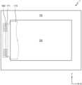
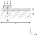
도 1은 본 발명의 일 실시예에 따른 표시 장치를 개략적으로 나타낸 평면도이다.
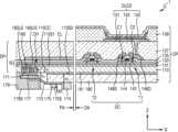
도 2는 도 1의 표시 장치의 후면의 일부를 개략적으로 나타낸 배면도이다.
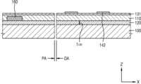
도 3은 도 1의 표시 장치를 제1방향(x)을 따라 취한 일부 단면도이다.
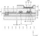
도 4는 도 1의 표시 장치를 제2방향(y)을 따라 취한 일부 단면도이다.
도 5a 내지 도 5k는 도 1의 표시 장치를 제조하는 방법을 순차적으로 나타낸 단면도들이다.
도 6은 본 발명의 다른 실시예에 따른 표시 장치의 주변 영역을 개략적으로 나타낸 단면도이다.
도 7은 본 발명의 또 다른 실시예에 따른 표시 장치의 주변 영역을 개략적으로 나타낸 단면도이다.
도 8은 본 발명의 또 다른 실시예에 따른 표시 장치의 주변 영역을 개략적으로 나타낸 단면도이다.
도 9a 내지 도 9c는 도 8의 표시 장치를 제조하는 방법의 일부를 순차적으로 나타낸 단면도들이다.
도 10은 본 발명의 또 다른 실시예에 따른 표시 장치의 주변 영역을 개략적으로 나타낸 단면도이다.
도 11a 및 도 11b는 일 실시예에 따른 도 10의 표시 장치를 제조하는 방법의 일부를 순차적으로 나타낸 단면도들이다.
도 12a 내지 도 12c는 다른 실시예에 따른 도 10의 표시 장치를 제조하는 방법의 일부를 순차적으로 나타낸 단면도들이다.
도 13은 본 발명의 또 다른 실시예에 따른 표시 장치의 주변 영역을 개략적으로 나타낸 단면도이다.FIG. 1 is a plan view schematically illustrating a display device according to one embodiment of the present invention.
Figure 2 is a rear view schematically showing a portion of the rear surface of the display device of Figure 1.
Figure 3 is a partial cross-sectional view of the display device of Figure 1 taken along the first direction (x).
Figure 4 is a partial cross-sectional view of the display device of Figure 1 taken along the second direction (y).
FIGS. 5A to 5K are cross-sectional views sequentially showing a method for manufacturing the display device of FIG. 1.
FIG. 6 is a cross-sectional view schematically illustrating a peripheral area of a display device according to another embodiment of the present invention.
FIG. 7 is a cross-sectional view schematically illustrating a peripheral area of a display device according to another embodiment of the present invention.
FIG. 8 is a cross-sectional view schematically illustrating a peripheral area of a display device according to another embodiment of the present invention.
FIGS. 9A to 9C are cross-sectional views sequentially showing part of a method for manufacturing the display device of FIG. 8.
FIG. 10 is a cross-sectional view schematically illustrating a peripheral area of a display device according to another embodiment of the present invention.
FIGS. 11A and 11B are cross-sectional views sequentially illustrating a part of a method for manufacturing the display device of FIG. 10 according to one embodiment.
FIGS. 12A to 12C are cross-sectional views sequentially illustrating part of a method for manufacturing the display device of FIG. 10 according to another embodiment.
FIG. 13 is a cross-sectional view schematically illustrating a peripheral area of a display device according to another embodiment of the present invention.
본 발명은 다양한 변환을 가할 수 있고 여러 가지 실시예를 가질 수 있는 바, 특정 실시예들을 도면에 예시하고 상세한 설명에 상세하게 설명하고자 한다. 본 발명의 효과 및 특징, 그리고 그것들을 달성하는 방법은 도면과 함께 상세하게 후술되어 있는 실시예들을 참조하면 명확해질 것이다. 그러나 본 발명은 이하에서 개시되는 실시예들에 한정되는 것이 아니라 다양한 형태로 구현될 수 있다.The present invention can be modified in various ways and has various embodiments, and specific embodiments are illustrated in the drawings and described in detail in the detailed description. The effects and features of the present invention and the methods for achieving them will become clear with reference to the embodiments described in detail below together with the drawings. However, the present invention is not limited to the embodiments disclosed below, and can be implemented in various forms.
이하, 첨부된 도면을 참조하여 본 발명의 실시예들을 상세히 설명하기로 하며, 도면을 참조하여 설명할 때 동일하거나 대응하는 구성 요소는 동일한 도면부호를 부여하고 이에 대한 중복되는 설명은 생략하기로 한다.Hereinafter, embodiments of the present invention will be described in detail with reference to the attached drawings. When describing with reference to the drawings, identical or corresponding components are given the same drawing reference numerals and redundant descriptions thereof will be omitted.
이하의 실시예에서 층, 막, 영역, 판 등의 각종 구성요소가 다른 구성요소 "상에" 있다고 할 때, 이는 다른 구성요소 "바로 상에" 있는 경우뿐 아니라 그 사이에 다른 구성요소가 개재된 경우도 포함한다. 또한 설명의 편의를 위하여 도면에서는 구성 요소들이 그 크기가 과장 또는 축소될 수 있다. 예컨대, 도면에서 나타난 각 구성의 크기 및 두께는 설명의 편의를 위해 임의로 나타내었으므로, 본 발명이 반드시 도시된 바에 한정되지 않는다.In the following examples, when various components such as layers, films, regions, and plates are said to be "on" other components, this includes not only cases where they are "directly on" other components, but also cases where other components are interposed between them. In addition, for convenience of explanation, the sizes of components in the drawings may be exaggerated or reduced. For example, the size and thickness of each component shown in the drawings are arbitrarily shown for convenience of explanation, and therefore the present invention is not necessarily limited to what is shown.
이하의 실시예에서, x축, y축 및 z축은 직교 좌표계 상의 세 축으로 한정되지 않고, 이를 포함하는 넓은 의미로 해석될 수 있다. 예를 들어, x축, y축 및 z축은 서로 직교할 수도 있지만, 서로 직교하지 않는 서로 다른 방향을 지칭할 수도 있다.In the following examples, the x-axis, y-axis, and z-axis are not limited to three axes on an orthogonal coordinate system, and may be interpreted in a broad sense that includes them. For example, the x-axis, y-axis, and z-axis may be orthogonal to each other, but may also refer to different directions that are not orthogonal to each other.
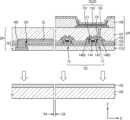
도 1은 본 발명의 일 실시예에 따른 표시 장치를 개략적으로 나타낸 평면도이고, 도 2는 도 1의 표시 장치의 후면의 일부를 개략적으로 나타낸 배면도이고, 도 3은 도 1의 표시 장치를 제1방향(x)을 따라 취한 일부 단면도이고, 도 4는 도 1의 표시 장치를 제2방향(y)을 따라 취한 일부 단면도이다.FIG. 1 is a plan view schematically showing a display device according to one embodiment of the present invention, FIG. 2 is a rear view schematically showing a portion of the rear surface of the display device of FIG. 1, FIG. 3 is a partial cross-sectional view of the display device of FIG. 1 taken along a first direction (x), and FIG. 4 is a partial cross-sectional view of the display device of FIG. 1 taken along a second direction (y).
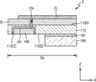
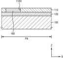
도 1 내지 도 4를 참조하면, 일 실시예에 따른 표시 장치(1)는 제1면(110S1) 및 제1면(110S1)에 반대되며 오목부(110CC)를 포함하는 제2면(110S2)을 포함하는 제1플렉서블 기판(110), 제1플렉서블 기판(110)의 제1면(110S1) 상에 배치되며 적어도 하나의 트랜지스터(T1)를 포함하는 구동 회로부(DC), 제2면(110S2)에 포함된 오목부(110CC)에 배치되어일부가 노출된 도전 패턴(160), 도전 패턴(160)과 구동 회로부(DC)를 전기적으로 연결하는 도전선(CL), 구동 회로부(DC)에 의해 구동되는 발광 소자(OLED), 및 제1플렉서블 기판(110)의 제2면(110S2) 상에 도전 패턴(160)과 중첩하지 않도록 배치된 지지 기판(180)을 포함한다. 여기서, "제1 플렉서블 기판(110)의 제1면(110S1) 상"을 "제1 플렉서블 기판(110)의 상부"로 설정했을 때, "제1 플렉서블 기판(110)의 제2면(110S2) 상"은 "제1 플렉서블 기판(110)의 하부"로 해석될 수 있다.Referring to FIGS. 1 to 4, a display device (1) according to one embodiment includes a first flexible substrate (110) including a first surface (110S1) and a second surface (110S2) opposite to the first surface (110S1) and including a concave portion (110CC), a driving circuit (DC) disposed on the first surface (110S1) of the first flexible substrate (110) and including at least one transistor (T1), a conductive pattern (160) disposed in the concave portion (110CC) included in the second surface (110S2) and having a partially exposed portion, a conductive line (CL) electrically connecting the conductive pattern (160) and the driving circuit (DC), a light-emitting element (OLED) driven by the driving circuit (DC), and a support substrate (180) disposed on the second surface (110S2) of the first flexible substrate (110) so as not to overlap the conductive pattern (160). Here, when “the first surface (110S1) of the first flexible substrate (110)” is set as “the upper part of the first flexible substrate (110),” “the second surface (110S2) of the first flexible substrate (110)” can be interpreted as “the lower part of the first flexible substrate (110).”
표시 장치(1)는 화상을 표시하는 표시 영역(DA)과 표시 영역(DA)의 적어도 일부를 둘러싸는 주변 영역(PA)을 포함하며, 표시 영역(DA)에는 광을 방출하는 복수의 발광 소자(OLED)들이 배치되고 주변 영역(PA)에는 발광 소자(OLED)를 구동시키는 구동 회로부(DC)에 전기적 신호를 전달하기 위한 도전선(CL)들을 패널 외부의 구동부와 연결하기 위한 패드, 즉 도전 패턴(160)이 배치될 수 있다.A display device (1) includes a display area (DA) for displaying an image and a peripheral area (PA) surrounding at least a portion of the display area (DA). A plurality of light-emitting elements (OLEDs) that emit light are arranged in the display area (DA), and pads, i.e. conductive patterns (160), for connecting conductive lines (CLs) for transmitting electrical signals to a driving circuit (DC) for driving the light-emitting elements (OLEDs) to a driving unit outside the panel can be arranged in the peripheral area (PA).
일 실시예에 따르면, 도전 패턴(160)은 표시 패널(DP)의 후면(back surface)에 적어도 일부가 외부로 노출되도록 배치될 수 있다. 도전 패턴(160)은 표시 영역(DA)에 배치된 복수의 화소들을 구동하기 위한 복수의 도전선(CL)들과 각각 연결된 복수의 도전 패턴(160)들을 포함할 수 있다. 복수의 도전 패턴(160)들은 스캔 신호를 전달하는 스캔선과 연결된 도전 패턴, 데이터 신호를 전달하는 데이터선과 연결된 도전 패턴, 및 구동 전압을 인가하기 위한 전압선과 연결된 도전 패턴 중 적어도 하나를 포함할 수 있다. 여기서, 표시 패널(DP)의 후면은 화상이 표시되는 면의 반대면을 의미한다.According to one embodiment, the conductive pattern (160) may be arranged on the back surface of the display panel (DP) so that at least a portion thereof is exposed to the outside. The conductive pattern (160) may include a plurality of conductive patterns (160) each connected to a plurality of conductive lines (CL) for driving a plurality of pixels arranged in the display area (DA). The plurality of conductive patterns (160) may include at least one of a conductive pattern connected to a scan line for transmitting a scan signal, a conductive pattern connected to a data line for transmitting a data signal, and a conductive pattern connected to a voltage line for applying a driving voltage. Here, the back surface of the display panel (DP) means a surface opposite to a surface on which an image is displayed.
도 3을 참조하면, 도전 패턴(160) 상에 제1플렉서블 기판(110)이 배치된다. 도전 패턴(160)이 표시 패널(DP)의 후면에 노출되어야 하므로, 제1플렉서블 기판(110)은 도전 패턴(160)의 하면(160LS)이 노출되도록 도전 패턴(160)을 덮을 수 있다. 즉, 제1플렉서블 기판(110)은 도전 패턴(160)의 상면(160US) 및 옆면을 덮을 수 있다. 일 실시예에 따르면, 제1플렉서블 기판(110)은 제1면(110S1)에 반대되는 제2면(110S2)에 오목부(110CC)를 포함하며, 도전 패턴(160)의 적어도 일부는 오목부(110CC)에 배치될 수 있다. 따라서, 도전 패턴(160)의 적어도 일부는 제1플렉서블 기판(110)에 매립될 수 있다.Referring to FIG. 3, a first flexible substrate (110) is disposed on a conductive pattern (160). Since the conductive pattern (160) should be exposed to the rear surface of the display panel (DP), the first flexible substrate (110) can cover the conductive pattern (160) so that a lower surface (160LS) of the conductive pattern (160) is exposed. That is, the first flexible substrate (110) can cover the upper surface (160US) and the side surface of the conductive pattern (160). According to one embodiment, the first flexible substrate (110) includes a concave portion (110CC) on a second surface (110S2) opposite to the first surface (110S1), and at least a portion of the conductive pattern (160) can be disposed in the concave portion (110CC). Accordingly, at least a portion of the conductive pattern (160) can be embedded in the first flexible substrate (110).
제1플렉서블 기판(110)은 다양한 물질을 포함할 수 있는데, 예컨대 폴리에테르술폰(polyethersulphone, PES), 폴리아크릴레이트(polyacrylate, PAR), 폴리에테르 이미드(polyetherimide, PEI), 폴리에틸렌 나프탈레이트(polyethyelenen napthalate, PEN), 폴리에틸렌 테레프탈레이트(polyethyeleneterepthalate, PET), 폴리페닐렌 설파이드(polyphenylene sulfide, PPS), 폴리아릴레이트(polyallylate), 폴리이미드(polyimide, PI), 폴리카보네이트(polycarbonate, PC) 또는 셀룰로오스 아세테이트 프로피오네이트(cellulose acetate propionate, CAP)와 같은 고분자 수지를 포함할 수 있다. 일 실시예에 따르면, 제1플렉서블 기판(110)은 벤더블 특성이 우수한 폴리이미드(P1)로 구성될 수 있으며, 수 내지 수십 마이크로미터(μm)의 두께를 가질 수 있다.The first flexible substrate (110) may include various materials, for example, a polymer resin such as polyethersulphone (PES), polyacrylate (PAR), polyetherimide (PEI), polyethylene napthalate (PEN), polyethylene terephthalate (PET), polyphenylene sulfide (PPS), polyallylate, polyimide (PI), polycarbonate (PC), or cellulose acetate propionate (CAP). According to one embodiment, the first flexible substrate (110) may be made of polyimide (P1) having excellent bendable characteristics, and may have a thickness of several to several tens of micrometers (μm).
제1플렉서블 기판(110)의 제1면(110S1) 상에는 적어도 하나의 트랜지스터(T1)를 포함하는 구동 회로부(DC)가 배치되며, 트랜지스터(T1)는 비정질실리콘, 다결정실리콘 또는 유기반도체물질을 포함하는 활성층(142) 및 활성층(142)과 절연된 게이트전극(144)을 포함할 수 있다. 일 실시예에 따르면, 트랜지스터(T1)는 소스전극(146S) 및 드레인전극(146D)을 더 포함할 수 있으며, 소스전극(146S) 및 드레인전극(146D)은 콘택홀(C1, C2)을 통해 활성층(142)과 각각 전기적으로 연결될 수 있다.A driving circuit (DC) including at least one transistor (T1) is arranged on a first surface (110S1) of a first flexible substrate (110). The transistor (T1) may include an active layer (142) including amorphous silicon, polycrystalline silicon or an organic semiconductor material and a gate electrode (144) insulated from the active layer (142). According to one embodiment, the transistor (T1) may further include a source electrode (146S) and a drain electrode (146D), and the source electrode (146S) and the drain electrode (146D) may be electrically connected to the active layer (142) through contact holes (C1, C2), respectively.
활성층(142)과 게이트전극(144)의 절연성을 확보하기 위해, 실리콘옥사이드, 실리콘나이트라이드 및/또는 실리콘옥시나이트라이드 등의 무기물을 포함하는 게이트절연층(133)이 활성층(142)과 게이트전극(144) 사이에 개재될 수 있다. 아울러 게이트전극(144)의 상부에는 실리콘옥사이드, 실리콘나이트라이드 및/또는 실리콘옥시나이트라이드 등의 무기물을 포함하는 층간절연층(135)이 배치될 수 있으며, 소스전극(146S) 및 드레인전극(1246D)은 그러한 층간절연층(135) 상에 배치될 수 있다.In order to secure insulation between the active layer (142) and the gate electrode (144), a gate insulating layer (133) including an inorganic material such as silicon oxide, silicon nitride and/or silicon oxynitride may be interposed between the active layer (142) and the gate electrode (144). In addition, an interlayer insulating layer (135) including an inorganic material such as silicon oxide, silicon nitride and/or silicon oxynitride may be disposed on the upper portion of the gate electrode (144), and the source electrode (146S) and the drain electrode (1246D) may be disposed on the interlayer insulating layer (135).
구동 회로부(DC)는 상술한 트랜지스터(T1) 이외에 스위칭 기능을 하는 트랜지스터(T2) 및 기타 다양한 기능을 하는 복수의 트랜지스터와 커패시터 등을 더 포함할 수 있으며, 구동 회로부(DC)는 발광 소자(OLED)에 전기적으로 연결되어 발광 소자(OLED)를 구동할 수 있다.The driving circuit (DC) may further include, in addition to the above-described transistor (T1), a transistor (T2) having a switching function, a plurality of transistors and capacitors having various other functions, and the driving circuit (DC) may be electrically connected to the light-emitting element (OLED) to drive the light-emitting element (OLED).
이러한 구조의 트랜지스터(T1)와 제1플렉서블 기판(110) 사이에는 실리콘옥사이드, 실리콘나이트라이드 및/또는 실리콘옥시나이트라이드 등과 같은 무기물을 포함하는 버퍼층(131)이 개재될 수 있다. 이러한 버퍼층(131)은 제1플렉서블 기판(110)의 상면의 평활성을 높이거나 제1플렉서블 기판(110) 등으로부터의 불순물이 트랜지스터(T1)의 활성층(142)으로 침투하는 것을 방지하거나 최소화하는 역할을 할 수 있다.A buffer layer (131) including an inorganic material such as silicon oxide, silicon nitride, and/or silicon oxynitride may be interposed between the transistor (T1) of this structure and the first flexible substrate (110). This buffer layer (131) may serve to increase the smoothness of the upper surface of the first flexible substrate (110) or prevent or minimize impurities from the first flexible substrate (110) or the like from penetrating into the active layer (142) of the transistor (T1).
트랜지스터(T1) 상에는 평탄화층(137)이 배치될 수 있다. 예컨대 도 3에 도시된 것과 같이 트랜지스터(T1) 상부에 유기발광소자가 배치될 경우, 평탄화층(137)은 트랜지스터(T1)를 포함하는 구동 회로부(DC)의 상부를 평탄화하는 역할을 할 수 있다. 이러한 평탄화층(137)은 예컨대 아크릴, 폴리이미드, BCB(Benzocyclobutene) 또는 HMDSO(hexamethyldisiloxane) 등과 같은 유기물로 형성될 수 있다. 도 3에서는 버퍼층(131), 게이트절연층(133), 층간절연층(135), 및 평탄화층(137)이 단층으로 도시되어 있으나, 이들은 2개 이상의 층으로 구성될 수도 있다.A planarization layer (137) may be arranged on the transistor (T1). For example, when an organic light-emitting element is arranged on the transistor (T1) as illustrated in FIG. 3, the planarization layer (137) may play a role in planarizing the upper portion of the driving circuit (DC) including the transistor (T1). This planarization layer (137) may be formed of an organic material such as acrylic, polyimide, BCB (Benzocyclobutene), or HMDSO (hexamethyldisiloxane). In FIG. 3, the buffer layer (131), the gate insulating layer (133), the interlayer insulating layer (135), and the planarization layer (137) are illustrated as a single layer, but they may be composed of two or more layers.
제1플렉서블 기판(110)의 제1면(110S1) 상에는 도전선(CL)이 배치될 수 있다. 도전선(CL)은 구동 회로부(DC) 및 도전 패턴(160)과 각각 전기적으로 연결되어, 구동 회로부(DC)와 도전 패턴(160)을 전기적으로 연결하는 기능을 한다. 구동 회로부(DC)는 복수의 트랜지스터, 커패시터 및 이들을 연결하는 연결선 등을 모두 포함하는 개념으로 도전선(CL)은 구동 회로부(DC)에 스캔 신호, 데이터 신호 또는 전압을 인가하는 배선일 수 있다. 도 4에 도시된 바와 같이 도전선(CL)은 서로 분리되어 있는 복수의 도전선(CL)들을 포함하고, 도전 패턴(160)은 복수의 도전선(CL)들 각각과 연결되며 서로 분리되어 있는 복수의 도전 패턴(160)들을 포함할 수 있다.A conductive line (CL) may be arranged on the first surface (110S1) of the first flexible substrate (110). The conductive line (CL) is electrically connected to the driving circuit (DC) and the conductive pattern (160), respectively, and functions to electrically connect the driving circuit (DC) and the conductive pattern (160). The driving circuit (DC) is a concept that includes a plurality of transistors, capacitors, and connection lines connecting them, and the conductive line (CL) may be a wiring that applies a scan signal, a data signal, or a voltage to the driving circuit (DC). As illustrated in FIG. 4, the conductive line (CL) includes a plurality of conductive lines (CL) that are separated from each other, and the conductive pattern (160) may include a plurality of conductive patterns (160) that are connected to each of the plurality of conductive lines (CL) and are separated from each other.
복수의 도전선(CL)들은 스캔선, 데이터선, 및 구동 전압선 중 어느 하나일 수 있으며, 스캔선, 데이터선 및 구동 전압선이 혼합되어 있을 수도 있다. 또, 복수의 도전선(CL)들은 동일층에 배치될 수도 있고, 서로 다른 층들에 배치될 수도 있다. 물론, 복수의 도전선(CL)들 각각은 서로 절연되도록 구성된다. 도 4에 도시하진 않았지만, 복수의 도전선(CL)들은 도전성 접착제(177)에 의해 연결 소자(171)에 포함된 단자와 정렬 및 연결될 수 있다. 도 4에서는 도전성 접착제(177), 연결 소자(171), 연성 회로 기판(173), 및 보호층(179)은 도시하지 않고, 주변 영역(PA)에 배치된 일부 구성만을 도시하였다.The plurality of conductive lines (CL) may be any one of scan lines, data lines, and driving voltage lines, and the scan lines, data lines, and driving voltage lines may be mixed. In addition, the plurality of conductive lines (CL) may be arranged in the same layer or may be arranged in different layers. Of course, each of the plurality of conductive lines (CL) is configured to be insulated from each other. Although not shown in FIG. 4, the plurality of conductive lines (CL) may be aligned and connected to terminals included in the connecting element (171) by a conductive adhesive (177). In FIG. 4, the conductive adhesive (177), the connecting element (171), the flexible circuit board (173), and the protective layer (179) are not shown, and only some components arranged in the peripheral area (PA) are shown.
일 실시예에 따르면, 도전선(CL)은 트랜지스터(T1)의 소스전극(146S) 및 드레인전극(146D)과 동일층에 배치되며, 이들과 동일물질로 구성될 수 있다. 예컨대, 도전선(CL)은 데이터 신호를 전달하는 데이터선일 수 있으며, 티타늄(Ti)을 포함하는 제1층, 알루미늄(Al)을 포함하는 제2층 및 티타늄(Ti)을 포함하는 제3층을 포함할 수 있다. 그러나, 본 발명은 이에 한정되지 않으며 도전선(CL)은 알루미늄(Al), 백금(Pt), 팔라듐(Pd), 은(Ag), 마그네슘(Mg), 금(Au), 니켈(Ni), 네오디뮴(Nd), 이리듐(Ir), 크롬(Cr), 리튬(Li), 칼슘(Ca), 몰리브덴(Mo), 티타늄(Ti), 텅스텐(W), 구리(Cu) 중 하나 이상의 물질로 단층 또는 다층으로 형성될 수 있다. 그러나, 본 발명은 이에 한정되지 않으며, 도전선(CL)은 게이트전극(144)과 동일층에 배치되며, 게이트전극(144)과 동일한 물질로 구성될 수도 있다. 예컨대, 게이트전극(144) 및 도전선(CL)은 몰리브덴(Mo)의 단일층으로 구성될 수 있다.According to one embodiment, the conductive line (CL) is arranged on the same layer as the source electrode (146S) and the drain electrode (146D) of the transistor (T1), and may be composed of the same material as them. For example, the conductive line (CL) may be a data line that transmits a data signal, and may include a first layer including titanium (Ti), a second layer including aluminum (Al), and a third layer including titanium (Ti). However, the present invention is not limited thereto, and the conductive line (CL) may be formed as a single layer or multiple layers of one or more materials from aluminum (Al), platinum (Pt), palladium (Pd), silver (Ag), magnesium (Mg), gold (Au), nickel (Ni), neodymium (Nd), iridium (Ir), chromium (Cr), lithium (Li), calcium (Ca), molybdenum (Mo), titanium (Ti), tungsten (W), and copper (Cu). However, the present invention is not limited thereto, and the conductive line (CL) may be arranged on the same layer as the gate electrode (144) and may be composed of the same material as the gate electrode (144). For example, the gate electrode (144) and the conductive line (CL) may be composed of a single layer of molybdenum (Mo).
도시하진 않았지만, 도전선(CL)은 표시 영역(DA)으로부터 주변 영역(PA)까지 연장될 수 있으며, 도전선(CL)의 적어도 일부는 도전 패턴(160)과 평면상 중첩될 수 있다.Although not illustrated, the challenge line (CL) may extend from the display area (DA) to the peripheral area (PA), and at least a portion of the challenge line (CL) may overlap the challenge pattern (160) in a plane.
도전선(CL)과 도전 패턴(160)의 사이에는 절연 구조체(IS) 및 제1플렉서블 기판(110)의 적어도 일부가 배치될 수 있으며, 절연 구조체(IS) 및 제1플렉서블 기판(110)에 형성된 콘택홀(CH)을 통해 도전선(CL)과 도전 패턴(160)이 전기적으로 연결될 수 있다. 도 3에서, 절연 구조체(IS)는 버퍼층(131), 게이트절연층(133), 층간절연층(135)을 포함하는 구조체를 의미하나, 본 발명은 이에 한정되지 않으며 절연 구조체(IS)는 버퍼층, 게이트절연층, 층간절연층, 및 추가적인 절연층 중 적어도 하나를 포함하는 층을 의미할 수 있다. 즉, 다른 도면에 도시된 절연 구조체(IS)는 버퍼층(131), 게이트절연층(133) 및 층간절연층(135)을 포함하는 구조체로 한정되지 않는다.An insulating structure (IS) and at least a part of the first flexible substrate (110) may be arranged between the conductive line (CL) and the conductive pattern (160), and the conductive line (CL) and the conductive pattern (160) may be electrically connected through a contact hole (CH) formed in the insulating structure (IS) and the first flexible substrate (110). In FIG. 3, the insulating structure (IS) means a structure including a buffer layer (131), a gate insulating layer (133), and an interlayer insulating layer (135), but the present invention is not limited thereto, and the insulating structure (IS) may mean a layer including at least one of a buffer layer, a gate insulating layer, an interlayer insulating layer, and an additional insulating layer. That is, the insulating structure (IS) illustrated in other drawings is not limited to a structure including a buffer layer (131), a gate insulating layer (133), and an interlayer insulating layer (135).
층간절연층(135) 상의 표시 영역(DA)에는 발광 소자(OLED)가 배치될 수 있다. 도 3에서는 발광 소자(OLED)가 유기 발광 소자인 경우를 예시하였지만 본 발명은 이에 한정되지 않으며, 발광 소자(OLED)의 위치 또한 층간절연층(135)의 상부로 한정되지 않는다.A light-emitting element (OLED) may be placed in the display area (DA) on the interlayer insulating layer (135). In Fig. 3, the case where the light-emitting element (OLED) is an organic light-emitting element is exemplified, but the present invention is not limited thereto, and the position of the light-emitting element (OLED) is also not limited to the upper portion of the interlayer insulating layer (135).
발광 소자(OLED)는 화소전극(151), 대향전극(155) 및 그 사이에 개재되며 발광층을 포함하는 중간층(153)을 포함한다. 화소전극(151)은 평탄화층(137)에 형성된 개구를 통해 소스전극(146S) 및 드레인전극(146D) 중 어느 하나와 컨택하여 트랜지스터(T1)와 전기적으로 연결된다.The light-emitting element (OLED) includes a pixel electrode (151), a counter electrode (155), and an intermediate layer (153) interposed therebetween and including a light-emitting layer. The pixel electrode (151) is electrically connected to the transistor (T1) by contacting one of the source electrode (146S) and the drain electrode (146D) through an opening formed in the planarization layer (137).
평탄화층(137) 상부에는 화소정의막(139)이 배치될 수 있다. 이 화소정의막(139)은 적어도 화소전극(151)의 중앙부가 노출되도록 하는 개구를 가짐으로써 화소를 정의하는 역할을 한다. 또한, 화소정의막(139)은 화소전극(151)의 가장자리와 화소전극(151) 상부의 대향전극(155)과의 사이의 거리를 증가시킴으로써 화소전극(151)의 가장자리에서 아크(arc) 등이 발생하는 것을 방지하는 역할을 한다. 이와 같은 화소정의막(139)은 예컨대 폴리이미드 또는 HMDSO(hexamethyldisiloxane) 등과 같은 유기물로 형성될 수 있다.A pixel definition film (139) may be arranged on the planarization layer (137). This pixel definition film (139) has an opening that exposes at least the central portion of the pixel electrode (151), thereby defining a pixel. In addition, the pixel definition film (139) prevents an arc or the like from occurring at the edge of the pixel electrode (151) by increasing the distance between the edge of the pixel electrode (151) and the counter electrode (155) on the upper portion of the pixel electrode (151). Such a pixel definition film (139) may be formed of an organic material, such as polyimide or HMDSO (hexamethyldisiloxane), for example.
화소전극(151)은 반사층을 포함하는 반사 전극일 수 있다. 예컨대, 반사층은 은(Ag), 마그네슘(Mg), 알루미늄(Al), 백금(Pt), 팔라듐(Pd), 금(Au), 니켈(Ni), 네오디뮴(Nd), 이리듐(Ir) 및 크롬(Cr)을 포함하는 그룹에서 선택된 적어도 어느 하나를 포함할 수 있으며, 반사층 상에는 인듐틴옥사이드(ITO: indium tin oxide), 인듐징크옥사이드(IZO: indium zinc oxide), 징크옥사이드(ZnO: zinc oxide), 인듐옥사이드(In2O3: indium oxide), 인듐갈륨옥사이드(IGO: indium galium oxide) 및 알루미늄징크옥사이드(AZO: aluminium zinc oxide)를 포함하는 그룹에서 선택된 적어도 어느 하나로 형성된 투명 또는 반투명 전극층이 더 배치될 수 있다.The pixel electrode (151) may be a reflective electrode including a reflective layer. For example, the reflective layer may include at least one selected from the group consisting of silver (Ag), magnesium (Mg), aluminum (Al), platinum (Pt), palladium (Pd), gold (Au), nickel (Ni), neodymium (Nd), iridium (Ir), and chromium (Cr), and a transparent or semitransparent electrode layer formed of at least one selected from the group consisting of indium tin oxide (ITO), indium zinc oxide (IZO), zinc oxide (ZnO), indium oxide (In2 O3 : indium oxide), indium gallium oxide (IGO), and aluminum zinc oxide (AZO) may be further disposed on the reflective layer.
일 실시예에 따르면, 화소전극(151)은 ITO/Ag/ITO의 3개의 층으로 구성될 수 있다.According to one embodiment, the pixel electrode (151) may be composed of three layers of ITO/Ag/ITO.
발광 소자(OLED)의 중간층(153)은 유기 발광층을 포함하며, 그 외에 정공 주입층(HIL: Hole Injection Layer), 정공 수송층(HTL: Hole Transport Layer), 전자 수송층(ETL: Electron Transport Layer) 및 전자 주입층(EIL: Electron Injection Layer) 중 적어도 하나를 더 포함할 수 있다. 그러나, 본 발명은 이에 한정되지 않으며, 중간층(153)은 기타 다양한 기능층을 더 포함할 수 있다.The intermediate layer (153) of the light-emitting element (OLED) includes an organic light-emitting layer, and may further include at least one of a hole injection layer (HIL), a hole transport layer (HTL), an electron transport layer (ETL), and an electron injection layer (EIL). However, the present invention is not limited thereto, and the intermediate layer (153) may further include various other functional layers.
물론 중간층(153)은 반드시 이에 한정되는 것은 아니고, 다양한 구조를 가질 수도 있음은 물론이다. 그리고 중간층(153)은 복수 개의 화소전극(151)들에 걸쳐서 일체인 층을 포함할 수도 있고, 복수 개의 화소전극(151)들 각각에 대응하도록 패터닝된 층을 포함할 수도 있다.Of course, the intermediate layer (153) is not necessarily limited to this, and may have various structures. In addition, the intermediate layer (153) may include a layer that is integral across a plurality of pixel electrodes (151), or may include a layer patterned to correspond to each of the plurality of pixel electrodes (151).
한편, 유기 발광층은 백색광을 방출할 수 있도록 적색 발광층, 녹색 발광층 및 청색 발광층이 적층된 다층 구조를 갖거나, 적색 발광 물질, 녹색 발광 물질 및 청색 발광 물질을 포함한 단일층 구조를 가질 수 있다. 이와 같은 유기 발광층을 구비한 유기발광소자는 적색 컬러 필터, 녹색 컬러 필터 및 청색 컬러 필터를 추가로 구비함으로써, 풀 컬러를 방출할 수 있다.Meanwhile, the organic light-emitting layer may have a multilayer structure in which a red light-emitting layer, a green light-emitting layer, and a blue light-emitting layer are laminated so as to emit white light, or may have a single layer structure including a red light-emitting material, a green light-emitting material, and a blue light-emitting material. An organic light-emitting device having such an organic light-emitting layer can emit full color by additionally having a red color filter, a green color filter, and a blue color filter.
대향전극(155)은 (반)투명 전극일 수 있다. 예컨대, 대향전극(155)은 은(Ag), 알루미늄(Al), 마그네슘(Mg), 리튬(Li), 칼슘(Ca), 구리(Cu), LiF/Ca, LiF/Al, MgAg 및 CaAg에서 선택된 하나 이상의 물질을 포함할 수 있으며, 광을 투과시킬 수 있도록 수 내지 수십 nm의 두께를 갖는 박막으로 형성될 수 있다. 일 실시예에 따르면, 발광 소자(OLED)는 표시 패널(DP)의 전면, 즉 제3방향(z)으로 광을 방출하는 전면 발광형일 수 있다.The counter electrode (155) may be a (semi)transparent electrode. For example, the counter electrode (155) may include one or more materials selected from silver (Ag), aluminum (Al), magnesium (Mg), lithium (Li), calcium (Ca), copper (Cu), LiF/Ca, LiF/Al, MgAg, and CaAg, and may be formed as a thin film having a thickness of several to several tens of nm so as to transmit light. According to one embodiment, the light-emitting element (OLED) may be a front-emitting type that emits light in the front side of the display panel (DP), i.e., in the third direction (z).
발광 소자(OLED) 상에는 발광 소자(OLED)를 덮는 봉지층(미도시)이 배치될 수 있으며, 봉지층(미도시)은 발광 소자(OLED)를 외부로부터의 수분이나 산소 등으로부터 보호할 수 있다.An encapsulation layer (not shown) covering the light-emitting element (OLED) may be placed on the light-emitting element (OLED), and the encapsulation layer (not shown) can protect the light-emitting element (OLED) from moisture or oxygen from the outside.
제1플렉서블 기판(110)의 제2면(110S2)의 하부에는 지지 기판(180)이 배치될 수 있다. 여기서 하부는 제1플렉서블 기판(110)의 발광 소자(OLED)가 배치된 방향의 반대쪽 방향을 의미한다.A support substrate (180) may be placed on the lower side of the second surface (110S2) of the first flexible substrate (110). Here, the lower side means the direction opposite to the direction in which the light-emitting element (OLED) of the first flexible substrate (110) is placed.
지지 기판(180)은 제1플렉서블 기판(110)에 비하여 큰 강도(stiffness)를 갖으며, 예컨대 폴리에테르술폰(polyethersulphone, PES), 폴리아크릴레이트(polyacrylate, PAR), 폴리에테르 이미드(polyetherimide, PEI), 폴리에틸렌 나프탈레이트(polyethyelenen napthalate, PEN), 폴리에틸렌 테레프탈레이트(polyethyeleneterepthalate, PET), 폴리페닐렌 설파이드(polyphenylene sulfide, PPS), 폴리아릴레이트(polyallylate), 폴리이미드(polyimide, PI), 폴리카보네이트(polycarbonate, PC) 또는 셀룰로오스 아세테이트 프로피오네이트(cellulose acetate propionate, CAP)와 같은 고분자 수지를 포함할 수 있다. 일 실시예에 따르면, 지지 기판(200)은 폴리에틸렌 나프탈레이트(PEN) 또는 폴리에틸렌 테레프탈레이트(PET)로 구성될 수 있으며, 폴리이미드(PI)로 구성된 제1플렉서블 기판(110)보다 큰 두께를 가질 수 있다.The support substrate (180) has greater stiffness than the first flexible substrate (110) and may include a polymer resin such as, for example, polyethersulphone (PES), polyacrylate (PAR), polyetherimide (PEI), polyethyelenen napthalate (PEN), polyethyeleneterepthalate (PET), polyphenylene sulfide (PPS), polyallylate, polyimide (PI), polycarbonate (PC), or cellulose acetate propionate (CAP). According to one embodiment, the support substrate (200) may be composed of polyethylene naphthalate (PEN) or polyethylene terephthalate (PET) and may have a thickness greater than that of the first flexible substrate (110) composed of polyimide (PI).
지지 기판(180)과 제1플렉서블 기판(110)의 사이에는 접착층(181)이 배치될 수 있다. 후술하겠지만, 지지 기판(180)은 제1플렉서블 기판(110) 상에 구동 회로부(DC) 및 발광 소자(OLED) 등을 형성한 후 후속 공정을 통해 제1플렉서블 기판(110)의 제2면(110S2)에 형성되는 구성 요소로서, 예컨대, 접착층(181)을 이용하여 제1플렉서블 기판(110)의 제2면(110S2) 상에 지지 기판(180)을 부착할 수 있다.An adhesive layer (181) may be placed between the support substrate (180) and the first flexible substrate (110). As will be described later, the support substrate (180) is a component formed on the second surface (110S2) of the first flexible substrate (110) through a subsequent process after forming a driving circuit (DC) and a light-emitting element (OLED) on the first flexible substrate (110). For example, the support substrate (180) may be attached on the second surface (110S2) of the first flexible substrate (110) using the adhesive layer (181).
상기 지지 기판(180)은 도전 패턴(160)이 배치된 영역에는 배치되지 않는다. 즉, 지지 기판(180)은 도전 패턴(160)을 노출하도록 배치될 수 있다. 즉, 지지 기판(180)과 도전 패턴(160)은 서로 평면상 중첩되지 않도록 배치될 수 있다.The above-mentioned support substrate (180) is not placed in an area where the conductive pattern (160) is placed. That is, the support substrate (180) may be placed so as to expose the conductive pattern (160). That is, the support substrate (180) and the conductive pattern (160) may be placed so as not to overlap each other on a plane.
표시 패널(DP)의 후면, 즉 제1플렉서블 기판(110)에 의해 하면(160LS)이 노출된 도전 패턴(160)은 메인 회로부(174)와 도전 패턴(160)을 전기적으로 연결하기 위한 연성 회로 기판(173)과 전기적으로 연결된다. 일 실시예에 따르면, 도전 패턴(160)과 연성 회로 기판(173)은 연결 소자(171)에 의해 전기적으로 연결되며, 연결 소자(171)와 도전 패턴(160)의 사이에는 도전성 접착제(177)가 배치될 수 있다. 이때, 전자칩(175)은 연성 회로 기판(173)에 배치될 수 있다.The conductive pattern (160) exposed on the back surface of the display panel (DP), that is, the lower surface (160LS) by the first flexible substrate (110), is electrically connected to a flexible circuit board (173) for electrically connecting the main circuit unit (174) and the conductive pattern (160). According to one embodiment, the conductive pattern (160) and the flexible circuit board (173) are electrically connected by a connecting element (171), and a conductive adhesive (177) may be disposed between the connecting element (171) and the conductive pattern (160). At this time, the electronic chip (175) may be disposed on the flexible circuit board (173).
그러나, 도 3에 도시된 도전 패턴(160)과 메인 회로부(174)의 연결 구조를 예시적인 것으로, 본 발명은 이에 한정되지 않는다. 즉, 다른 실시예에 따르면, 도전 패턴(160) 상에 전자칩(175)이 배치되고, 연성 회로 기판(173)에 의해 전자칩(175)과 메인 회로부(174)가 전기적으로 연결될 수도 있다. 연결 수단은 도전성 접착제(177) 이외에 커넥터 등이 사용될 수 있다.However, the connection structure of the conductive pattern (160) and the main circuit unit (174) illustrated in Fig. 3 is exemplary, and the present invention is not limited thereto. That is, according to another embodiment, an electronic chip (175) may be placed on the conductive pattern (160), and the electronic chip (175) and the main circuit unit (174) may be electrically connected by a flexible circuit board (173). In addition to a conductive adhesive (177), a connector or the like may be used as a connection means.
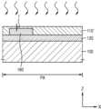
일 실시예에 따르면, 도전 패턴(160) 및 연성 회로 기판(173)의 적어도 일부 상에는 노출된 금속 등을 보호하기 위한 보호층(179)이 배치될 수 있다. 상기 보호층(179)은 실리콘 등으로 구성된 무기 절연층일 수 있다. 도 2에 도시된 바와 같이, 보호층(179)은 연성 회로 기판(173)의 가장자리의 적어도 일부를 덮도록 배치될 수 있다.According to one embodiment, a protective layer (179) may be disposed on at least a portion of the challenge pattern (160) and the flexible circuit board (173) to protect exposed metal, etc. The protective layer (179) may be an inorganic insulating layer made of silicon, etc. As illustrated in FIG. 2, the protective layer (179) may be disposed to cover at least a portion of an edge of the flexible circuit board (173).
도 3을 참조하면, 보호층(179) 및 전자칩(175)은 연성 회로 기판(173)의 외측, 즉 연성 회로 기판(173)의 하부에 배치된다. 이 경우, 보호층(179)의 하면(179S)보다 전자칩(175)의 하면(175S)이 제1플렉서블 기판(110)의 제2면(110S2)에 더 가깝게 배치될 수 있다. 이는 전자칩(175)을 보호하기 위해 보호층(179)을 외부 충격에 대한 범퍼로서 기능하도록 한 것으로, 전자칩(175)의 하면(175S)은 보호층(179)의 하면(179S)보다 소정의 높이(?h)만큼 제1플렉서블 기판(110)의 제2면에 가깝게 위치할 수 있다. 즉, 보호층(179)의 하면(179S)과 제1플렉서블 기판(110)의 제2면(110S2) 사이의 거리(h1)는 전자칩(175)의 하면(175S)과 제1플렉서블 기판(110)의 제2면(110S2) 사이의 거리(h2)보다 클 수 있다. 여기서, 기준 위치인 제1플렉서블 기판(110)의 제2면(110S2)은 제2면(110S2) 중 오목부(110CC)가 배치된 영역 이외의 영역을 의미한다.Referring to FIG. 3, the protective layer (179) and the electronic chip (175) are arranged on the outer side of the flexible circuit board (173), that is, on the lower side of the flexible circuit board (173). In this case, the lower side (175S) of the electronic chip (175) may be arranged closer to the second surface (110S2) of the first flexible substrate (110) than the lower side (179S) of the protective layer (179). This is to allow the protective layer (179) to function as a bumper against external impact in order to protect the electronic chip (175), and the lower side (175S) of the electronic chip (175) may be positioned closer to the second surface of the first flexible substrate (110) by a predetermined height (?h) than the lower side (179S) of the protective layer (179). That is, the distance (h1) between the lower surface (179S) of the protective layer (179) and the second surface (110S2) of the first flexible substrate (110) may be greater than the distance (h2) between the lower surface (175S) of the electronic chip (175) and the second surface (110S2) of the first flexible substrate (110). Here, the second surface (110S2) of the first flexible substrate (110), which is the reference position, means an area other than an area of the second surface (110S2) where the concave portion (110CC) is arranged.
도 3을 참조하면, 제1플렉서블 기판(110)은 오목부(110CC)를 제외한 영역에서 제1두께(t1)를 가지며 도전 패턴(160)은 제2두께(t2)를 가질 수 있으며, 제2두께(t2)는 약 700 nm 이하의 값을 가질 수 있다. 상기 도전 패턴(160)의 상부에 배치된 제1플렉서블 기판(110)은 제3두께(t3)를 가진다. 도 3에서는 제3두께(t3)가 제1두께(t1)와 제2두께(t2)의 차이와 실질적으로 동일한 것으로 도시되어 있으나, 본 발명은 이에 한정되지 않는다. 즉, 도전 패턴(160)이 제1플렉서블 기판(110) 내에 매립된 정도 및 제1플렉서블 기판(110)의 상면의 굴곡 형태에 따라 제3두께(t3)는 다양한 값을 가질 수 있다.Referring to FIG. 3, the first flexible substrate (110) has a first thickness (t1 ) in an area excluding a concave portion (110CC), and the conductive pattern (160) may have a second thickness (t2 ), and the second thickness (t2 ) may have a value of about 700 nm or less. The first flexible substrate (110) disposed on the conductive pattern (160) has a third thickness (t3 ). In FIG. 3 , the third thickness (t3 ) is illustrated as being substantially the same as the difference between the first thickness (t1 ) and the second thickness (t2 ), but the present invention is not limited thereto. That is, the third thickness (t3 ) can have various values depending on the degree to which the challenge pattern (160) is embedded in the first flexible substrate (110) and the curved shape of the upper surface of the first flexible substrate (110 ).
일 실시예에 따르면, 제1플렉서블 기판(110)은 감광성 유기물을 포함할 수 있으며, 이 경우 제3두께(t3)의 두께와 무관하게 제1플렉서블 기판(110)에 도전선(CL)과 도전 패턴(160)을 연결하기 위한 콘택홀(CH)에 대응되는 개구를 포토 리소그래피 등의 방법을 통해 용이하게 형성할 수 있다. 상기 콘택홀(CH)에 대응되는 개구에 의해 도전 패턴(160)의 일부가 노출될 수 있다.According to one embodiment, the first flexible substrate (110) may include a photosensitive organic material, and in this case, regardless of the thickness of the third thickness (t3 ), an opening corresponding to a contact hole (CH) for connecting a conductive line (CL) and a conductive pattern (160) to the first flexible substrate (110) may be easily formed through a method such as photolithography. A portion of the conductive pattern (160) may be exposed by the opening corresponding to the contact hole (CH).
그러나, 다른 실시예에 따르면, 제1플렉서블 기판(110)은 감광성 유기물이 아닌 유기물을 포함할 수 있으며, 이 경우 제3두께(t3)는 제1두께(t1)보다 매우 작은 값, 예컨대 수 내지 수백 나노미터(nm)의 값을 가질 수 있다.However, according to another embodiment, the first flexible substrate (110) may include an organic material other than a photosensitive organic material, in which case the third thickness (t3 ) may have a value much smaller than the first thickness (t1 ), for example, a value of several to several hundred nanometers (nm).
제3두께(t3)를 매우 작게 형성함으로써 제1플렉서블 기판(110)의 콘택홀(CH)에 대응되는 영역을 플라즈마 처리 및 에싱(ashing) 등의 공정을 통해 완전히 제거함으로써, 콘택홀(CH)에 대응되는 개구를 형성할 수 있다. 제3두께(t3)가 작은 값을 갖도록 제1플렉서블 기판(110)을 구성하는 유기물, 예컨대 폴리이미드의 점도는 20000 cp 이하일 수 있다. 즉, 점도가 낮은 유기물을 이용하여 도전 패턴(160)을 덮는 제1플렉서블 기판(110)을 형성함으로써, 도전 패턴(160) 상부에 배치된 제1플렉서블 기판(110)의 제3두께(t3)가 매우 작은 값을 갖도록 할 수 있다. 일 실시예에 따르면, 도전 패턴(160)의 제2두께(t2)의 약 1/4의 두께를 가질 수 있으며 약 150 nm 이하의 값을 가질 수 있다. 상기 구성에 의해 도전 패턴(160) 상에 배치된 제1플렉서블 기판(110)을 플라즈마 처리 및 에싱을 통해 용이하게 제거할 수 있다.By forming the third thickness (t3 ) very small, an area corresponding to the contact hole (CH) of the first flexible substrate (110) can be completely removed through a process such as plasma treatment and ashing, thereby forming an opening corresponding to the contact hole (CH). In order for the third thickness (t3 ) to have a small value, the viscosity of the organic material constituting the first flexible substrate (110), for example, polyimide, can be 20,000 cp or less. That is, by forming the first flexible substrate (110) covering the conductive pattern (160) using an organic material having low viscosity, the third thickness (t3 ) of the first flexible substrate (110) disposed on the conductive pattern (160) can be made to have a very small value. According to one embodiment, it can have a thickness of about 1/4 of the second thickness (t2 ) of the conductive pattern (160) and can have a value of about 150 nm or less. The first flexible substrate (110) placed on the challenge pattern (160) by the above configuration can be easily removed through plasma treatment and ashing.
또 다른 실시예에 따르면 제3두께(t3)는 0일 수 있으며, 이에 대해서는 후술한다.According to another embodiment, the third thickness (t3 ) can be zero, as described below.
상술한 표시 장치(1)는 표시 패널(CP)의 후면에 노출된 도전 패턴(160)을 포함하며 상기 도전 패턴(160)에 연성 회로 기판(173) 등을 연결시킴으로써, 표시 장치(1)의 주변 영역(PA)의 면적을 최소화할 수 있다.The above-described display device (1) includes a conductive pattern (160) exposed on the rear surface of the display panel (CP), and by connecting a flexible circuit board (173), etc. to the conductive pattern (160), the area of the peripheral area (PA) of the display device (1) can be minimized.
도 5a 내지 도 5k는 도 1의 표시 장치를 제조하는 방법을 순차적으로 나타낸 단면도들이다.FIGS. 5A to 5K are cross-sectional views sequentially showing a method for manufacturing the display device of FIG. 1.
도 5a를 참조하면, 유리 등으로 구성된 캐리어 기판(100) 상에 제2플렉서블 기판(120)을 형성한 후 제2플렉서블 기판(120) 상에 도전 패턴(160)을 형성한다. 상기 제2플렉서블 기판(120)은 제1플렉서블 기판(110)과 동일한 물질을 포함할 수 있으며, 예컨대, 제2플렉서블 기판(120)은 폴리이미드(P1)로 구성될 수 있으며, 약 0.1 μm 이하의 두께(t120)를 가질 수 있다. 제2플렉서블 기판(120)의 두께(t120)를 약 0.1 μm 이하로 형성함으로써, 캐리어 기판(100)을 제거하면서 제2플렉서블 기판(120)을 같이 제거할 수 있다. 이에 관해서는 후술한다.Referring to FIG. 5A, a second flexible substrate (120) is formed on a carrier substrate (100) made of glass or the like, and then a conductive pattern (160) is formed on the second flexible substrate (120). The second flexible substrate (120) may include the same material as the first flexible substrate (110). For example, the second flexible substrate (120) may be made of polyimide (P1) and may have a thickness (t120 ) of about 0.1 μm or less. By forming the thickness (t120 ) of the second flexible substrate (120) to be about 0.1 μm or less, the second flexible substrate (120) may be removed together with the carrier substrate (100). This will be described later.
도 5b를 참조하면, 제2플렉서블 기판(120) 상에 도전 패턴(160)을 덮도록 제1플렉서블 기판(110)을 형성한다. 제1플렉서블 기판(110)은 폴리이미드로 구성될 수 있다. 제1플렉서블 기판(110)은 제1두께(t1)를 가지며, 제1두께(t1)는 수 내지 수십 마이크로미터(μm)의 값을 가질 수 있다. 즉, 제1플렉서블 기판(110)의 제1두께(t1)는 제2플렉서블 기판(120)의 두께(t120)보다 클 수 있다.Referring to FIG. 5b, a first flexible substrate (110) is formed to cover a conductive pattern (160) on a second flexible substrate (120). The first flexible substrate (110) may be made of polyimide. The first flexible substrate (110) has a first thickness (t1 ), and the first thickness (t1 ) may have a value of several to several tens of micrometers (μm). That is, the first thickness (t1 ) of the first flexible substrate (110) may be greater than the thickness (t 120 ) of the second flexible substrate (120 ).
제1플렉서블 기판(110)의 제2면(110S2)에는 도전 패턴(160)에 의해 오목부(110CC)가 형성될 수 있다. 즉, 도전 패턴(160)의 적어도 일부가 제1플렉서블 기판(110)의 오목부(110CC)에 매립된 형태가 될 수 있다. 이때, 도전 패턴(160)은 제2두께(t2)를 가지며 제1플렉서블 기판(110)의 오목부(110CC)에 대응되는 영역은 제3두께(t3)를 가질 수 있다.A concave portion (110CC) may be formed on the second surface (110S2) of the first flexible substrate (110) by the conductive pattern (160). That is, at least a portion of the conductive pattern (160) may be embedded in the concave portion (110CC) of the first flexible substrate (110). At this time, the conductive pattern (160) may have a second thickness (t2 ), and an area corresponding to the concave portion (110CC) of the first flexible substrate (110) may have a third thickness (t3 ).
도 5c를 참조하면, 제1플렉서블 기판(110) 상에 버퍼층(131) 및 트랜지스터(T1)의 활성층(142)을 형성할 수 있다. 버퍼층(131)은 실리콘옥사이드, 실리콘나이트라이드 및/또는 실리콘옥시나이트라이드 등과 같은 무기물을 포함하며, 단층 또는 다층일 수 있다. 활성층(142)은 비정질 실리콘, 다정질 실리콘 또는 산화물 등을 포함할 수 있다.Referring to FIG. 5c, a buffer layer (131) and an active layer (142) of a transistor (T1) can be formed on a first flexible substrate (110). The buffer layer (131) includes an inorganic material such as silicon oxide, silicon nitride, and/or silicon oxynitride, and can be a single layer or multilayer. The active layer (142) can include amorphous silicon, polycrystalline silicon, or an oxide.
도 5d를 참조하면, 버퍼층(131) 상에 활성층(142)을 덮는 게이트절연층(133)을 형성하고, 게이트절연층(133) 상에 게이트전극(144)을 형성할 수 있다. 게이트전극(144)을 형성한 후, 게이트절연층(133) 상에 게이트전극(144)을 덮는 층간절연층(135)을 형성할 수 있다. 게이트절연층(133) 및 층간절연층(135)은 실리콘옥사이드, 실리콘나이트라이드 및/또는 실리콘옥시나이트라이드 등의 무기물을 포함하며 단층 또는 다층으로 형성될 수 있다. 게이트전극(144)은 몰리브덴(Mo)의 단일층으로 형성될 수 있으나, 이에 제한되진 않는다.Referring to FIG. 5d, a gate insulating layer (133) covering an active layer (142) may be formed on a buffer layer (131), and a gate electrode (144) may be formed on the gate insulating layer (133). After forming the gate electrode (144), an interlayer insulating layer (135) covering the gate electrode (144) may be formed on the gate insulating layer (133). The gate insulating layer (133) and the interlayer insulating layer (135) may include an inorganic material such as silicon oxide, silicon nitride, and/or silicon oxynitride, and may be formed as a single layer or multiple layers. The gate electrode (144) may be formed as a single layer of molybdenum (Mo), but is not limited thereto.
도 5e를 참조하면, 게이트절연층(133) 및 층간절연층(135)에 소스전극(146S) 및 드레인전극(146D)을 각각 활성층(142)에 연결하기 위한 콘택홀(C1, C2)을 형성할 수 있다. 이와 동시에, 도전 패턴(160)의 상부에 배치된 버퍼층(131), 게이트절연층(133) 및 층간절연층(135) 각각에 콘택홀(CH)을 형성하기 위한 개구를 형성할 수 있다. 버퍼층(131), 게이트절연층(133) 및 층간절연층(135)은 모두 무기물로 구성되므로, 단일 포토 리소그래피 공정을 통해 동시에 개구를 형성할 수 있다.Referring to FIG. 5e, contact holes (C1, C2) for connecting the source electrode (146S) and the drain electrode (146D) to the active layer (142) can be formed in the gate insulating layer (133) and the interlayer insulating layer (135), respectively. At the same time, openings for forming contact holes (CH) can be formed in the buffer layer (131), the gate insulating layer (133), and the interlayer insulating layer (135) arranged on the upper portion of the conductive pattern (160), respectively. Since the buffer layer (131), the gate insulating layer (133), and the interlayer insulating layer (135) are all composed of inorganic materials, the openings can be formed simultaneously through a single photolithography process.
도 5f를 참조하면, 제1플렉서블 기판(110)에 도전 패턴(160)의 상면의 일부를 노출하는 개구를 형성할 수 있다. 제1플렉서블 기판(110)은 감광성 유기물인 경우 포토 리소그래피 공정을 통해 제1플렉서블 기판(110)에 개구를 형성할 수 있다. 따라서, 버퍼층(131), 게이트절연층(133), 층간절연층(135) 및 제1플렉서블 기판(110)에 각각 형성되며 평면상 중첩되는 개구들의 결합에 의해 도전선(CL)을 도전 패턴(160)에 연결하기 위한 콘택홀(CH)이 형성될 수 있다.Referring to FIG. 5f, an opening exposing a portion of an upper surface of a conductive pattern (160) may be formed in the first flexible substrate (110). If the first flexible substrate (110) is a photosensitive organic material, the opening may be formed in the first flexible substrate (110) through a photolithography process. Accordingly, a contact hole (CH) for connecting a conductive line (CL) to a conductive pattern (160) may be formed by combining openings that are formed in the buffer layer (131), the gate insulating layer (133), the interlayer insulating layer (135), and the first flexible substrate (110) and overlap each other in a plane.
제1플렉서블 기판(110)이 감광성 유기물이 아닌 유기물인 경우, 제1플렉서블 기판(110)의 오목부(110CC)에 대응되는 영역의 제3두께(t3)는 매우 작은 값, 예컨대 역 150 nm 이하의 값을 가질 수 있다.When the first flexible substrate (110) is an organic material other than a photosensitive organic material, the third thickness (t3 ) of the area corresponding to the concave portion (110CC) of the first flexible substrate (110) may have a very small value, for example, a value of 150 nm or less.
상기 제3두께(t3)를 매우 작게 구성함으로써, 제1플렉서블 기판(110)의 버퍼층(131), 게이트절연층(133) 및 층간절연층(135)에 형성된 개구를 통해 노출된 영역을 플라즈마 처리 및 에싱 등의 공정을 통해 용이하게 제거할 수 있다.By configuring the third thickness (t3 ) to be very small, the area exposed through the opening formed in the buffer layer (131), gate insulating layer (133), and interlayer insulating layer (135) of the first flexible substrate (110) can be easily removed through processes such as plasma treatment and ashing.
도 5g를 참조하면, 층간절연층(135) 상에 트랜지스터(T1)의 소스전극(146S), 드레인전극(146D) 및 도전선(CL)을 형성할 수 있다. 도전선(CL)은 데이터 신호를 전달하는 데이터선일 수 있으며, 티타늄(Ti)을 포함하는 제1층, 알루미늄(Al)을 포함하는 제2층 및 티타늄(Ti)을 포함하는 제3층을 포함할 수 있다. 그러나, 본 발명은 이에 한정되지 않으며, 도전선(CL)은 다양한 물질로 단층 또는 다층으로 형성될 수 있다. 또한, 도전선(CL)은 소스전극(146S) 및 드레인전극(146D)과 동일 공정이 아닌, 게이트전극(144)과 동일한 공정을 통해 형성될 수도 있으며, 도전선(CL)은 데이터선이 아닌 스캔선 등 다양한 신호를 전달하는 배선일 수 있다.Referring to FIG. 5g, a source electrode (146S), a drain electrode (146D), and a conductive line (CL) of a transistor (T1) may be formed on an interlayer insulating layer (135). The conductive line (CL) may be a data line that transmits a data signal, and may include a first layer including titanium (Ti), a second layer including aluminum (Al), and a third layer including titanium (Ti). However, the present invention is not limited thereto, and the conductive line (CL) may be formed as a single layer or multiple layers using various materials. In addition, the conductive line (CL) may be formed through the same process as the gate electrode (144), not through the same process as the source electrode (146S) and the drain electrode (146D), and the conductive line (CL) may be a wiring that transmits various signals, such as a scan line, not a data line.
도 5h를 참조하면, 층간절연층(135) 상에 트랜지스터(T1) 등을 포함하는 구동 회로부(DC)를 덮는 평탄화층(137)을 형성한 후, 표시 영역(DA) 내의 평탄화층(137) 상에 화소전극(151) 및 화소전극(151)의 중앙부를 노출하는 개구를 포함하는 화소정의막(139)을 형성할 수 있다. 화소정의막(139)에 포함된 개구에 의해 노출된 화소전극(151) 상에 발광층을 포함하는 중간층(153) 및 대향전극(155)을 형성할 수 있으며, 이러한 구성을 통해 표시 영역(DA)에 발광 소자(OLED)를 형성할 수 있다.Referring to FIG. 5h, after forming a planarization layer (137) covering a driving circuit (DC) including a transistor (T1), etc., on an interlayer insulating layer (135), a pixel definition film (139) including a pixel electrode (151) and an opening exposing a central portion of the pixel electrode (151) can be formed on the planarization layer (137) within the display area (DA). An intermediate layer (153) including a light-emitting layer and a counter electrode (155) can be formed on the pixel electrode (151) exposed by the opening included in the pixel definition film (139), and a light-emitting element (OLED) can be formed in the display area (DA) through this configuration.
도 5i 및 도 5j를 참조하면, 캐리어 기판(100)의 하부로부터 캐리어 기판(100)에 레이저를 조사함으로써 캐리어 기판(100)과 제2플렉서블 기판(120)을 제1플렉서블 기판(110)으로부터 제거할 수 있다.Referring to FIGS. 5i and 5j, the carrier substrate (100) and the second flexible substrate (120) can be removed from the first flexible substrate (110) by irradiating the carrier substrate (100) with a laser from the lower portion of the carrier substrate (100).
제2플렉서블 기판(120)의 두께(t120)는 상술한 바와 같이 약 0.1 μm 이하일 수 있으며, 캐리어 기판(100)을 제거하는 공정 중 제2플렉서블 기판(120)이 함께 제거될 수 있다. 즉, 제2플렉서블 기판(120)이 레이저 조사에 의해 특성이 변화되어 제1플렉서블 기판(110)에 대한 접착력이 없어서 캐리어 기판(100)과 같이 제거되는 희생층으로 기능할 수 있다. 캐리어 기판(100)과 제2플렉서블 기판(120)을 제거함으로써 도전 패턴(160)이 표시 패널(DP)의 후면에 노출될 수 있다.The thickness (t120 ) of the second flexible substrate (120) may be about 0.1 μm or less as described above, and the second flexible substrate (120) may be removed together during the process of removing the carrier substrate (100). That is, since the second flexible substrate (120) has a characteristic changed by laser irradiation and has no adhesive force to the first flexible substrate (110), it may function as a sacrificial layer that is removed together with the carrier substrate (100). By removing the carrier substrate (100) and the second flexible substrate (120), the conductive pattern (160) may be exposed to the rear surface of the display panel (DP).
도 5k를 참조하면, 제1플렉서블 기판(110)의 제2면(110S2)의 하부에 접착층(181)을 이용하여 지지 기판(180)을 형성할 수 있다. 이때, 지지 기판(180)은 도전 패턴(160)이 배치된 영역에는 형성되지 않는다. 따라서, 지지 기판(180)에 의해 도전 패턴(160)이 덮이지 않고, 표시 패널(DP)의 후면에 노출될 수 있다.Referring to FIG. 5k, a support substrate (180) may be formed on the lower side of the second surface (110S2) of the first flexible substrate (110) using an adhesive layer (181). At this time, the support substrate (180) is not formed in the area where the conductive pattern (160) is arranged. Accordingly, the conductive pattern (160) may not be covered by the support substrate (180) and may be exposed to the rear side of the display panel (DP).
다시 도 3을 참조하면, 노출된 도전 패턴(160)에 도전성 접착제(177)을 이용하여 연결 소자(171) 및 연성 회로 기판(173) 등을 연결하고, 이들을 보호하기 위해 보호층(179)을 형성할 수 있다.Referring again to FIG. 3, a connecting element (171) and a flexible circuit board (173) can be connected to an exposed conductive pattern (160) using a conductive adhesive (177), and a protective layer (179) can be formed to protect them.
이하에서 설명하는 도면들은 다른 실시예들에 따른 표시 장치의 주변 영역(PA)의 일부 구성들만을 도시하고 있으며, 표시 장치의 표시 영역(DA, 도 3) 및 표시 패널(CP, 도 3)에 본딩(bonding)된 외부 회로 단자 등의 다른 구성은 도 3과 동일하거나, 도 3으로부터 공지의 기술을 토대로 변형된 구성을 가질 수 있다.The drawings described below illustrate only some configurations of a peripheral area (PA) of a display device according to other embodiments, and other configurations, such as a display area (DA, FIG. 3) of the display device and an external circuit terminal bonded to a display panel (CP, FIG. 3), may be the same as FIG. 3 or may have a modified configuration based on a known technology from FIG. 3.
도 6은 본 발명의 다른 실시예에 따른 표시 장치의 주변 영역을 개략적으로 나타낸 단면도이고, 도 7은 본 발명의 또 다른 실시예에 따른 표시 장치의 주변 영역을 개략적으로 나타낸 단면도이다.FIG. 6 is a cross-sectional view schematically showing a peripheral area of a display device according to another embodiment of the present invention, and FIG. 7 is a cross-sectional view schematically showing a peripheral area of a display device according to still another embodiment of the present invention.
도 6을 참조하면, 표시 장치(2)는 제2면(110S2)에 위치하는 오목부(110CC)를 포함하는 제1플렉서블 기판(110)을 포함하며, 오목부(110CC)에는 도전 패턴(160)이 배치된다. 즉, 도전 패턴(160)의 적어도 일부는 제1플렉서블 기판(110)에 매립되어 있다.Referring to FIG. 6, the display device (2) includes a first flexible substrate (110) including a concave portion (110CC) positioned on a second surface (110S2), and a conductive pattern (160) is arranged in the concave portion (110CC). That is, at least a portion of the conductive pattern (160) is embedded in the first flexible substrate (110).
도전 패턴(160)과 제1플렉서블 기판(110)의 사이에는 유착층(adhesion layer, 161)이 배치될 수 있으며, 유착층(161)은 도전 패턴(160)이 제1플렉서블 기판(110)으로부터 쉽게 분리되지 않도록 해주는 기능을 한다. 즉, 도전 패턴(160)과 제1플렉서블 기판(110) 사이의 결합력보다, 도전 패턴(160)과 유착층(161) 사이의 결합력 및 유착층(161)과 제1플렉서블 기판(110) 사이의 결합력이 더 크며, 유착층(161)은 상기 조건을 만족하는 물질로 구성될 수 있다.An adhesion layer (161) may be arranged between the conductive pattern (160) and the first flexible substrate (110), and the adhesion layer (161) has a function of preventing the conductive pattern (160) from being easily separated from the first flexible substrate (110). That is, the adhesion between the conductive pattern (160) and the adhesion layer (161) and the adhesion between the adhesion layer (161) and the first flexible substrate (110) are greater than the adhesion between the conductive pattern (160) and the first flexible substrate (110), and the adhesion layer (161) may be composed of a material that satisfies the above conditions.
일 실시예에 따르면, 유착층(161)은 금속 및 유기물로 구성된 제1플렉서블 기판(110) 각각과 강하게 결합될 수 있는 무기 절연층일 수 있으며, 예컨대 SiNx 또는 A-Si:H 등일 수 있다. 다른 실시예에 따르면, 유착층(161)은 HMDS(Hexamethyldisilazane) 또는 HMDSO(hexamethyldisiloxane) 등과 같은 유기물로 구성될 수도 있다.According to one embodiment, the adhesion layer (161) may be an inorganic insulating layer that can be strongly bonded to each of the first flexible substrates (110) composed of a metal and an organic material, and may be, for example, SiNx or A-Si:H. According to another embodiment, the adhesion layer (161) may be composed of an organic material, such as HMDS (Hexamethyldisilazane) or HMDSO (hexamethyldisiloxane).
이러한 유착층(161)은 도전 패턴(160)의 상면 및 옆면을 덮도록 형성되어, 도전 패턴(160)이 제1플렉서블 기판(110)으로부터 쉽게 분리되지 않도록 할 수 있다.This adhesion layer (161) is formed to cover the upper surface and side surfaces of the conductive pattern (160), thereby preventing the conductive pattern (160) from being easily separated from the first flexible substrate (110).
도 7을 참조하면, 유착층(161')은 도전 패턴(160)의 상면 및 옆면뿐만 아니라 제1플렉서블 기판(110)의 제2면(110S2) 전체를 덮도록 배치될 수도 있다. 이 경우, 지지 기판(180)과 제1플렉서블 기판(110)의 사이에도 유착층(161')이 배치될 수 있다.Referring to FIG. 7, the adhesion layer (161') may be arranged to cover not only the upper surface and the side surface of the conductive pattern (160), but also the entire second surface (110S2) of the first flexible substrate (110). In this case, the adhesion layer (161') may also be arranged between the support substrate (180) and the first flexible substrate (110).
도 6 및 도 7을 참조하면, 유착층(161, 161') 상에 제1플렉서블 기판(110)이 배치되고, 제1플렉서블 기판(110)의 제1면(110S1) 상에 절연 구조체(IS)가 배치되며, 절연 구조체(IS) 상에 도전선(CL)이 배치된다.Referring to FIGS. 6 and 7, a first flexible substrate (110) is placed on an adhesion layer (161, 161'), an insulating structure (IS) is placed on a first surface (110S1) of the first flexible substrate (110), and a conductive line (CL) is placed on the insulating structure (IS).
도전선(CL)은 절연 구조체(IS), 제1플렉서블 기판(110) 및 유착층(161, 161')에 형성된 콘택홀(CH)을 통해 도전 패턴(160)과 연결될 수 있다. 또한, 이러한 표시 장치(2, 3)를 제조하는 방법은, 도 5a 내지 도 5k에 도시된 방법과 실질적으로 동일 또는 유사하며, 도 5b의 단계 전에 유착층(161, 161')을 형성하는 단계를 더 포함할 수 있다. 즉, 유착층(161, 161')을 제2플렉서블 기판(120, 도 5a) 상에 도전 패턴(160)을 덮도록 형성한 후 제1플렉서블 기판(110)을 형성할 수 있다.The conductive line (CL) can be connected to the conductive pattern (160) through the contact hole (CH) formed in the insulating structure (IS), the first flexible substrate (110), and the adhesion layer (161, 161'). In addition, the method for manufacturing such a display device (2, 3) is substantially the same as or similar to the method illustrated in FIGS. 5A to 5K, and may further include a step of forming the adhesion layer (161, 161') before the step of FIG. 5B. That is, the adhesion layer (161, 161') can be formed on the second flexible substrate (120, FIG. 5A) to cover the conductive pattern (160), and then the first flexible substrate (110) can be formed.
도 5j 단계에서 캐리어 기판(100) 및 제2플렉서블 기판(120)을 제거하는 단계를 수행하며, 상기 유착층(161, 161')은 도전 패턴(160)과 제1플렉서블 기판(110) 사이의 결합력이 약해 제2플렉서블 기판(120)과 함께 도전 패턴(160)도 제1플렉서블 기판(110)으로부터 분리되지 않도록 하는 기능을 수행할 수 있다.In step 5j of FIG. 5, a step of removing the carrier substrate (100) and the second flexible substrate (120) is performed, and the adhesion layer (161, 161') can perform a function of preventing the conductive pattern (160) and the second flexible substrate (120) from being separated from the first flexible substrate (110) by weakening the bonding force between the conductive pattern (160) and the first flexible substrate (110).
캐리어 기판(100) 및 제2플렉서블 기판(120)을 제거한 후, 제1플렉서블 기판(110)의 제2면(110S2)의 하부에 지지 기판(180)을 형성하며, 제1플렉서블 기판(110)과 지지 기판(180) 사이에는 접착층(181)이 배치될 수 있다. 상기 접착층(181)은 지지 기판(180)을 제1플렉서블 기판(110)에 형성하는 방법에 따라 생략될 수도 있다.After removing the carrier substrate (100) and the second flexible substrate (120), a support substrate (180) is formed on the lower side of the second surface (110S2) of the first flexible substrate (110), and an adhesive layer (181) may be arranged between the first flexible substrate (110) and the support substrate (180). The adhesive layer (181) may be omitted depending on the method of forming the support substrate (180) on the first flexible substrate (110).
도 8은 본 발명의 또 다른 실시예에 따른 표시 장치의 주변 영역을 개략적으로 나타낸 단면도이고, 도 9a 내지 도 9c는 도 8의 표시 장치를 제조하는 방법의 일부를 순차적으로 나타낸 단면도들이다.FIG. 8 is a cross-sectional view schematically showing a peripheral area of a display device according to another embodiment of the present invention, and FIGS. 9a to 9c are cross-sectional views sequentially showing part of a method for manufacturing the display device of FIG. 8.
도 8을 참조하면, 표시 장치(4)는 제2면(110S2)에 위치하는 오목부(110CC)를 포함하는 제1플렉서블 기판(110)을 포함하며, 오목부(110CC)에는 도전 패턴(160)이 배치된다.Referring to FIG. 8, the display device (4) includes a first flexible substrate (110) including a concave portion (110CC) located on a second surface (110S2), and a conductive pattern (160) is arranged in the concave portion (110CC).
제1플렉서블 기판(110)의 제2면(110S2)의 하부에는 제2플렉서블 기판(120)이 배치된다. 제2플렉서블 기판(120)은 제1플렉서블 기판(110)과 동일한 물질을 포함할 수 있으며, 예컨대, 제1 및 제2플렉서블 기판(110, 120)은 폴리이미드(PI; polyimide)를 포함할 수 있다. 상기 제2플렉서블 기판(120)의 두께(t120)는 제1플렉서블 기판(110)의 제1두께(t1)보다 작을 수 있으며, 제2플렉서블 기판(120)은 도전 패턴(160)이 배치된 영역에는 배치되지 않을 수 있다. 즉, 제2플렉서블 기판(120)은 도전 패턴(160)을 노출하도록 제1플렉서블 기판(110)의 제2면(110S2)의 하부에 배치될 수 있다.A second flexible substrate (120) is arranged on a lower portion of a second surface (110S2) of a first flexible substrate (110). The second flexible substrate (120) may include the same material as the first flexible substrate (110). For example, the first and second flexible substrates (110, 120) may include polyimide (PI). The thickness (t120 ) of the second flexible substrate (120) may be smaller than the first thickness (t1 ) of the first flexible substrate (110), and the second flexible substrate (120) may not be arranged in an area where a conductive pattern (160) is arranged. That is, the second flexible substrate (120) can be placed on the lower side (110S2) of the first flexible substrate (110) to expose the conductive pattern (160).
제2플렉서블 기판(120)의 하부에는 지지 기판(180)이 배치되며, 제2플렉서블 기판(120)과 지지 기판(180)의 사이에는 접착층(181)이 배치될 수 있다. 지지 기판(180)은 제1 및 제2플렉서블 기판(110, 120)보다 강성이 큰 물질로 구성되며, 지지 기판(180)의 두께는 제2플렉서블 기판(120)의 두께(t120)보다 클 수 있다.A support substrate (180) is arranged on the lower side of the second flexible substrate (120), and an adhesive layer (181) may be arranged between the second flexible substrate (120) and the support substrate (180). The support substrate (180) is made of a material having greater rigidity than the first and second flexible substrates (110, 120), and the thickness of the support substrate (180) may be greater than the thickness (t120 ) of the second flexible substrate (120).
지지 기판(180)은 도전 패턴(160)이 배치된 영역에는 배치되지 않으며, 제2플렉서블 기판(120)의 적어도 일부를 노출하도록 배치될 수 있다.The support substrate (180) is not placed in the area where the challenge pattern (160) is placed, and may be placed so as to expose at least a portion of the second flexible substrate (120).
도 9a를 참조하면, 도 8의 표시 장치(4)를 제조하는 방법은, 도 5a 내지 도 5h에 순차적으로 도시된 바와 같은 제조 방법을 수행한 후, 캐리어 기판(100)의 하부로부터 레이저를 캐리어 기판(100)에 조사할 수 있다. 상기 도 9a에 도시된 제거 단계 전의 제2플렉서블 기판(120')은 도 5a에 도시된 제2플렉서블 기판(120)보다 큰 두께를 가질 수 있다.Referring to FIG. 9a, a method of manufacturing a display device (4) of FIG. 8 may include performing a manufacturing method as sequentially illustrated in FIGS. 5a to 5h, and then irradiating a laser to the carrier substrate (100) from the bottom of the carrier substrate (100). The second flexible substrate (120') before the removal step illustrated in FIG. 9a may have a greater thickness than the second flexible substrate (120) illustrated in FIG. 5a.
도 9b를 참조하면, 캐리어 기판(100) 및 제2플렉서블 기판(120')을 제거하는 단계를 수행할 수 있다. 이때, 제2플렉서블 기판(120')의 일부(120'')는 캐리어 기판(100)과 함께 제거되지만, 일부는 제거되지 않을 수 있다. 즉, 제1플렉서블 기판(110)의 제2면(110S2)의 하부에는 제2플렉서블 기판(120)이 남아있게 된다.Referring to FIG. 9b, a step of removing the carrier substrate (100) and the second flexible substrate (120') can be performed. At this time, a part (120'') of the second flexible substrate (120') is removed together with the carrier substrate (100), but a part may not be removed. That is, the second flexible substrate (120) remains on the lower part of the second surface (110S2) of the first flexible substrate (110).
도 9c를 참조하면, 제1플렉서블 기판(110)의 제2면(110S2)의 하부에 배치된 제2플렉서블 기판(120)의 도전 패턴(160)의 하부에 배치된 영역을 제거함으로써 도전 패턴(160)이 노출되도록 할 수 있다.Referring to FIG. 9c, the conductive pattern (160) can be exposed by removing the area disposed under the conductive pattern (160) of the second flexible substrate (120) disposed under the second surface (110S2) of the first flexible substrate (110).
제2플렉서블 기판(120)을 제거하는 공정은 포토 리소그래피 또는 기계적 방법 등을 통해 수행될 수 있다. 다시 도 8을 참조하면, 제2플렉서블 기판(120)의 하부에 접착층(181)을 이용하여 지지 기판(180)을 형성할 수 있다.The process of removing the second flexible substrate (120) can be performed through photolithography or a mechanical method, etc. Referring again to FIG. 8, a support substrate (180) can be formed using an adhesive layer (181) on the lower side of the second flexible substrate (120).
도 10은 본 발명의 또 다른 실시예에 따른 표시 장치의 주변 영역을 개략적으로 나타낸 단면도이고, 도 11a 및 도 11b는 일 실시예에 따른 도 10의 표시 장치를 제조하는 방법의 일부를 순차적으로 나타낸 단면도들이다.FIG. 10 is a cross-sectional view schematically illustrating a peripheral area of a display device according to another embodiment of the present invention, and FIGS. 11a and 11b are cross-sectional views sequentially illustrating a part of a method for manufacturing the display device of FIG. 10 according to one embodiment.
도 10을 참조하면, 일 실시예에 따른 표시 장치(5)는 제1면(110S1) 및 제1면(110S1)에 반대되며 개구부(110H)를 포함하는 제2면(110S2)을 포함하는 제1플렉서블 기판(110), 제1플렉서블 기판(110)의 제1면(110S1) 상에 배치되며 적어도 하나의 트랜지스터(T1, 도 3)를 포함하는 구동 회로부(DC, 도 3), 제2면(110S2)에 포함된 개구부(110H) 내에 배치되어 일부가 노출된 도전 패턴(160), 도전 패턴(160)과 구동 회로부(DC, 도 3)를 전기적으로 연결하는 도전선(CL), 구동 회로부(DC, 도 3)에 의해 구동되는 발광 소자(OLED, 도 3), 및 제1플렉서블 기판(110)의 제2면(110S2) 상에 도전 패턴(160)과 중첩하지 않도록 배치된 지지 기판(180)을 포함한다.Referring to FIG. 10, a display device (5) according to one embodiment includes a first flexible substrate (110) including a first surface (110S1) and a second surface (110S2) opposite to the first surface (110S1) and including an opening (110H), a driving circuit (DC, FIG. 3) disposed on the first surface (110S1) of the first flexible substrate (110) and including at least one transistor (T1, FIG. 3), a conductive pattern (160) disposed within the opening (110H) included in the second surface (110S2) and partially exposed, a conductive line (CL) electrically connecting the conductive pattern (160) and the driving circuit (DC, FIG. 3), a light-emitting element (OLED, FIG. 3) driven by the driving circuit (DC, FIG. 3), and a light-emitting element (OLED, FIG. 3) disposed on the second surface (110S2) of the first flexible substrate (110) so as not to overlap with the conductive pattern (160). It includes a deployed support substrate (180).
도 10의 표시 장치(5)는 다른 구성은 도 3의 표시 장치(1)와 실질적으로 동일하며, 제1플렉서블 기판(110)이 오목부(110CC)가 아닌 개구부(110H)를 포함하고 도전 패턴(160)이 개구부(110H)에 배치되어 있다는 차이점만 존재한다.The display device (5) of Fig. 10 is substantially the same as the display device (1) of Fig. 3 in other configurations, with the only difference being that the first flexible substrate (110) includes an opening (110H) rather than a concave portion (110CC) and the conductive pattern (160) is arranged in the opening (110H).
도전 패턴(160)은 금속을 포함하며 제1플렉서블 기판(110)은 폴리이미드 등의 유기물을 포함하므로, 도전 패턴(160)과 제1플렉서블 기판(110) 사이에 기포 등이 발생될 수 있다. 즉, 도전 패턴(160)과 제1플렉서블 기판(110) 사이의 결합력이 약해 도전 패턴(160)이 제1플렉서블 기판(110)으로부터 쉽게 분리될 수 있다.Since the conductive pattern (160) includes metal and the first flexible substrate (110) includes an organic material such as polyimide, air bubbles, etc. may be generated between the conductive pattern (160) and the first flexible substrate (110). That is, the bonding force between the conductive pattern (160) and the first flexible substrate (110) is weak, so the conductive pattern (160) may be easily separated from the first flexible substrate (110).
그러나, 도전 패턴(160)의 상면 상에 제1플렉서블 기판(110)이 배치되지 않고 바로 무기물을 포함하는 버퍼층(131, 도 3) 등을 포함하는 절연 구조체(IS)가 배치된 경우, 도전 패턴(160)과 절연 구조체(IS) 사이의 강한 결합력으로 인해 도전 패턴(160)이 표시 패널(DP, 도 3)으로부터 분리되지 않을 수 있다.However, if the first flexible substrate (110) is not placed on the upper surface of the conductive pattern (160) and an insulating structure (IS) including a buffer layer (131, FIG. 3) including an inorganic material is placed directly on the surface, the conductive pattern (160) may not be separated from the display panel (DP, FIG. 3) due to the strong bonding force between the conductive pattern (160) and the insulating structure (IS).
도 4를 참조하면, 제1플렉서블 기판(110)은 복수의 도전 패턴(160, 도 4)들이 각각 배치된 복수의 개구부(110H)들을 포함할 수 있으며, 도전 패턴(160)의 상면은 절연 구조체(IS)와 직접 접할 수 있다.Referring to FIG. 4, the first flexible substrate (110) may include a plurality of openings (110H) in which a plurality of conductive patterns (160, FIG. 4) are respectively arranged, and the upper surface of the conductive pattern (160) may be in direct contact with the insulating structure (IS).
상기 구성을 통해, 절연 구조체(IS) 상에 배치된 도전선(CL)과 도전 패턴(160)을 연결하기 위한 콘택홀(CH)을 용이하게 형성할 수 있다. 즉, 단일의 포토 리소그래피 공정을 통해 절연 구조체(IS)에 콘택홀(CH)을 형성하고, 절연 구조체(IS) 상에 도전선(CL)을 형성함으로써 도전 패턴(160)과 도전선(CL)을 연결할 수 있다.Through the above configuration, a contact hole (CH) for connecting a conductive line (CL) and a conductive pattern (160) arranged on an insulating structure (IS) can be easily formed. That is, a contact hole (CH) is formed in an insulating structure (IS) through a single photolithography process, and a conductive line (CL) is formed on the insulating structure (IS), thereby connecting the conductive pattern (160) and the conductive line (CL).
도 11a을 참조하면, 캐리어 기판(100) 상에 제2플렉서블 기판(120) 및 도전 패턴(160)을 형성한 후, 제2플렉서블 기판(120) 상에 제1플렉서블 기판(110)을 형성하기 위한 유기물(110')을 형성할 수 있다.Referring to FIG. 11a, after forming a second flexible substrate (120) and a conductive pattern (160) on a carrier substrate (100), an organic material (110') for forming a first flexible substrate (110) can be formed on the second flexible substrate (120).
상기 유기물(110')은 도전 패턴(160)의 상면 및 옆면을 덮을 수 있으며, 도전 패턴(160) 상에 배치된 유기물(110')의 두께(t)는 매우 작은 값을 가질 수 있다. 예컨대, 상기 두께(t)는 약 150 nm 이하의 값을 가질 수 있다. 유기물(110')을 형성한 후, 유기물(110') 상에 플라즈마 처리를 할 수 있다. 도전 패턴(160) 상에 배치된 유기물(110')의 두께(t)가 얇게 형성될 수 있도록, 유기물(110')은 약 20000 cp 이하의 점도를 갖는 물질로 구성될 수 있다.The organic material (110') can cover the upper surface and the side surface of the conductive pattern (160), and the thickness (t) of the organic material (110') disposed on the conductive pattern (160) can have a very small value. For example, the thickness (t) can have a value of about 150 nm or less. After the organic material (110') is formed, plasma treatment can be performed on the organic material (110'). In order for the thickness (t) of the organic material (110') disposed on the conductive pattern (160) to be formed thinly, the organic material (110') can be composed of a material having a viscosity of about 20,000 cp or less.
도 11b를 참조하면, 유기물(110')에 플라즈마 처리를 한 후, 에슁(ashing)을 함으로써 도전 패턴(160) 상에 배치된 유기물(110')을 제거함으로써 제1플렉서블 기판(110)을 형성할 수 있다. 상기 제1플렉서블 기판(110)은 도전 패턴(160)이 배치된 영역에 대응되는 개구부(110H)를 포함할 수 있다.Referring to FIG. 11b, after plasma treatment on an organic material (110'), the first flexible substrate (110) may be formed by removing the organic material (110') disposed on the conductive pattern (160) by performing ashing. The first flexible substrate (110) may include an opening (110H) corresponding to an area where the conductive pattern (160) is disposed.
도 12a 내지 도 12c는 다른 실시예에 따른 도 10의 표시 장치를 제조하는 방법의 일부를 순차적으로 나타낸 단면도들이다.FIGS. 12A to 12C are cross-sectional views sequentially illustrating part of a method for manufacturing the display device of FIG. 10 according to another embodiment.
도 12a 및 도 12b를 참조하면, 캐리어 기판(100) 상에 제2플렉서블 기판(120) 및 도전 패턴(160)을 형성한 후, 도전 패턴(160) 상에 소수성 처리를 할 수 있다. 상기 소수성 처리를 통해, 적어도 상기 도전 패턴(160)의 상면(160US)은 소수성을 띄게 된다.Referring to FIGS. 12a and 12b, after forming a second flexible substrate (120) and a conductive pattern (160) on a carrier substrate (100), a hydrophobic treatment may be performed on the conductive pattern (160). Through the hydrophobic treatment, at least the upper surface (160US) of the conductive pattern (160) becomes hydrophobic.
도 12c를 참조하면, 제2플렉서블 기판(120) 상에 제1플렉서블 기판(110)을 형성할 수 있다. 제1플렉서블 기판(110)은 낮은 점도를 가지는 물질로 형성될 수 있으며, 소수성 처리된 도전 패턴(160)의 상면(160US) 상에는 형성되지 않을 수 있다. 즉, 제1플렉서블 기판(110)은 도전 패턴(160)이 배치된 영역에 대응되는 개구부(110H)를 갖도록 형성될 수 있다.Referring to FIG. 12c, a first flexible substrate (110) may be formed on a second flexible substrate (120). The first flexible substrate (110) may be formed of a material having low viscosity, and may not be formed on the upper surface (160US) of the hydrophobic-treated conductive pattern (160). That is, the first flexible substrate (110) may be formed to have an opening (110H) corresponding to an area where the conductive pattern (160) is arranged.
다시 도 10을 참조하면, 제1플렉서블 기판(110) 상에 절연 구조체(IS)를 형성하고, 절연 구조체(IS)에 콘택홀(CH)을 형성한 후 절연 구조체(IS) 상에 도전선(CL)을 형성할 수 있다. 또한, 캐리어 기판(100) 및 제2플렉서블 기판(120)을 제거한 후, 제1플렉서블 기판(110)의 제2면(110S2) 상에 지지 기판(180)을 형성할 수 있다.Referring again to FIG. 10, an insulating structure (IS) may be formed on a first flexible substrate (110), a contact hole (CH) may be formed in the insulating structure (IS), and then a conductive line (CL) may be formed on the insulating structure (IS). In addition, after the carrier substrate (100) and the second flexible substrate (120) are removed, a support substrate (180) may be formed on the second surface (110S2) of the first flexible substrate (110).
도 13은 본 발명의 또 다른 실시예에 따른 표시 장치의 주변 영역을 개략적으로 나타낸 단면도이다.FIG. 13 is a cross-sectional view schematically illustrating a peripheral area of a display device according to another embodiment of the present invention.
도 13을 참조하면, 표시 장치(6)는 제2면(110S2)에 위치하는 개구부(110H)를 포함하는 제1플렉서블 기판(110)을 포함하며, 개구부(110H)에는 도전 패턴(160)이 배치된다.Referring to FIG. 13, the display device (6) includes a first flexible substrate (110) including an opening (110H) located on a second surface (110S2), and a conductive pattern (160) is arranged in the opening (110H).
제1플렉서블 기판(110)의 제2면(110S2)의 하부에는 제2플렉서블 기판(120)이 배치된다. 제2플렉서블 기판(120)은 제1플렉서블 기판(110)과 동일한 물질을 포함할 수 있으며, 예컨대, 제1 및 제2플렉서블 기판(110, 120)은 폴리이미드(PI; polyimide)를 포함할 수 있다. 제2플렉서블 기판(120)은 도전 패턴(160)이 배치된 영역에는 배치되지 않을 수 있다. 즉, 제2플렉서블 기판(120)은 도전 패턴(160)을 노출하도록 제1플렉서블 기판(110)의 제2면(110S2)의 하부에 배치될 수 있다.A second flexible substrate (120) is arranged under the second surface (110S2) of the first flexible substrate (110). The second flexible substrate (120) may include the same material as the first flexible substrate (110). For example, the first and second flexible substrates (110, 120) may include polyimide (PI). The second flexible substrate (120) may not be arranged in an area where the conductive pattern (160) is arranged. That is, the second flexible substrate (120) may be arranged under the second surface (110S2) of the first flexible substrate (110) so as to expose the conductive pattern (160).
제2플렉서블 기판(120)의 하부에는 지지 기판(180)이 배치되며, 제2플렉서블 기판(120)과 지지 기판(180)의 사이에는 접착층(181)이 배치될 수 있다. 지지 기판(180)은 제1 및 제2플렉서블 기판(110, 120)보다 강성이 큰 물질로 구성될 수 있다. 지지 기판(180)은 도전 패턴(160)이 배치된 영역에는 배치되지 않으며, 제2플렉서블 기판(120)의 적어도 일부를 노출하도록 배치될 수 있다.A support substrate (180) is arranged on the lower side of the second flexible substrate (120), and an adhesive layer (181) may be arranged between the second flexible substrate (120) and the support substrate (180). The support substrate (180) may be composed of a material having greater rigidity than the first and second flexible substrates (110, 120). The support substrate (180) is not arranged in an area where the conductive pattern (160) is arranged, and may be arranged to expose at least a portion of the second flexible substrate (120).
노출된 도전 패턴(160) 상에는 도 3에 도시된 바와 같이, 연성 회로 기판(173) 등이 연결되어 도전 패턴(160)과 표시 장치(6)를 제어하는 메인 회로부(174)를 전기적으로 연결할 수 있다.As shown in Fig. 3, a flexible circuit board (173) or the like is connected to the exposed challenge pattern (160) to electrically connect the challenge pattern (160) and the main circuit unit (174) that controls the display device (6).
상술한 실시예들에 따른 표시 장치(1, 2, 3, 4, 5, 6)는 표시 패널(CP)의 후면에 노출된 도전 패턴(160)을 포함하며 상기 도전 패턴(160)에 연성 회로 기판(173) 등을 연결시킴으로써, 표시 장치(1, 2, 3, 4, 5, 6)의 주변 영역(PA)의 면적을 최소화할 수 있다.The display devices (1, 2, 3, 4, 5, 6) according to the above-described embodiments include a conductive pattern (160) exposed on the rear surface of a display panel (CP), and by connecting a flexible circuit board (173), etc. to the conductive pattern (160), the area of the peripheral area (PA) of the display devices (1, 2, 3, 4, 5, 6) can be minimized.
또한, 상술한 실시예들에 따른 제조 방법에 따르면, 도전 패턴(160)이 표시 패널(CP)로부터 쉽게 분리되지 않고 도전 패턴(160)과 도전선(CL)을 연결하기 위한 콘택홀(CH)을 용이하게 형성할 수 있다.In addition, according to the manufacturing method according to the embodiments described above, the conductive pattern (160) is not easily separated from the display panel (CP) and a contact hole (CH) for connecting the conductive pattern (160) and the conductive line (CL) can be easily formed.
이와 같이 본 발명은 도면에 도시된 실시예를 참고로 설명되었으나 이는 예시적인 것에 불과하며, 당해 기술분야에서 통상의 지식을 가진 자라면 이로부터 다양한 변형 및 균등한 다른 실시예가 가능하다는 점을 이해할 것이다. 따라서 본 발명의 진정한 기술적 보호 범위는 첨부된 청구범위의 기술적 사상에 의하여 정해져야 할 것이다.Although the present invention has been described with reference to the embodiments shown in the drawings, these are merely exemplary, and those skilled in the art will understand that various modifications and equivalent other embodiments are possible. Therefore, the true technical protection scope of the present invention should be determined by the technical idea of the appended claims.
1, 2, 3, 4, 5, 6: 표시 장치DP: 표시 패널
IS: 절연 구조체CL: 도전선
OLED: 발광 소자DC: 구동 회로부
T1: 트랜지스터100: 캐리어 기판
110: 제1플렉서블 기판120: 제2플렉서블 기판
160: 도전 패턴171: 연결 소자
173: 연성 회로 기판174: 메인 회로부
175: 전자칩177: 도전성 접착제
179: 보호층180: 지지 부재1, 2, 3, 4, 5, 6: Display Device DP: Display Panel
IS: Insulating structure CL: Conducting wire
OLED: Light-emitting element DC: Driving circuit
T1: Transistor 100: Carrier substrate
110: First flexible substrate 120: Second flexible substrate
160: Challenge Pattern 171: Connecting Elements
173: Flexible circuit board 174: Main circuit board
175: Electronic Chip 177: Conductive Adhesive
179: Protective layer 180: Support member
Claims (25)
Translated fromKorean제1면 및 상기 제1면의 반대면인 제2면을 포함하고, 상기 주변 영역의상기 제2면은 오목부 또는 개구부를 포함하는 제1플렉서블 기판;
상기 제1면 상에 배치되며, 적어도 하나의 트랜지스터를 포함하는 구동 회로부;
상기 제2면의 상기 오목부 또는 개구부 내에 배치되어 일부가 노출된 도전 패턴;
상기 도전 패턴과 상기 제1플렉서블 기판 사이에 배치된 유착층(adhesion layer);
상기 도전 패턴과 상기 구동 회로부를 전기적으로 연결하는 도전선;
상기 표시 영역에 배치되며, 상기 구동 회로부에 의해 구동되는 발광 소자; 및
상기 제2면 상에, 상기 도전 패턴과 중첩하지 않도록 배치된 지지 기판을 포함하는, 표시 장치.In a display device including a display area and a peripheral area,
A first flexible substrate comprising a first side and a second side opposite to the first side, wherein the second side of the peripheral region includes a concave portion or an opening;
A driving circuit portion disposed on the first surface and including at least one transistor;
A challenge pattern positioned within the concave portion or opening of the second surface and partially exposed;
An adhesion layer disposed between the above challenge pattern and the first flexible substrate;
A conductive line electrically connecting the above-mentioned challenge pattern and the above-mentioned driving circuit unit;
A light emitting element disposed in the above display area and driven by the driving circuit unit; and
A display device comprising a support substrate positioned on the second surface so as not to overlap the challenge pattern.
상기 도전 패턴과 상기 도전선 사이에 배치된 절연 구조체를 포함하며,
상기 절연 구조체는 상기 도전 패턴과 상기 도전선을 연결하기 위한 콘택홀을 포함하는, 표시 장치.In the first paragraph,
Including an insulating structure arranged between the above challenge pattern and the above challenge line,
A display device, wherein the insulating structure includes a contact hole for connecting the conductive pattern and the conductive line.
상기 절연 구조체는 상기 제1플렉서블 기판 상에 순차적으로 배치된 버퍼층, 게이트 절연층 및 층간 절연층을 포함하며,
상기 트랜지스터는,
상기 버퍼층 상에 배치된 활성층 및 상기 게이트 절연층 상에 상기 활성층과 절연되도록 배치된 게이트 전극을 포함하는, 표시 장치.In the second paragraph,
The above insulating structure includes a buffer layer, a gate insulating layer, and an interlayer insulating layer sequentially arranged on the first flexible substrate,
The above transistor,
A display device comprising an active layer disposed on the buffer layer and a gate electrode disposed on the gate insulating layer so as to be insulated from the active layer.
상기 도전선은 상기 구동 회로부에 스캔 신호를 인가하는 스캔선 또는 데이터 신호를 인가하는 데이터선이며, 상기 게이트 전극과 동일층 또는 상기 층간 절연층 상에 배치된, 표시 장치.In the third paragraph,
The above-mentioned conductive line is a scan line for applying a scan signal to the driving circuit or a data line for applying a data signal, and is a display device arranged on the same layer as the gate electrode or on the interlayer insulating layer.
상기 유착층은 SiNx 또는 A-Si:H로 구성된 무기 절연 물질을 포함하는, 표시 장치.In the first paragraph,
A display device, wherein the above-mentioned adhesion layer comprises an inorganic insulating material composed of SiNx or A-Si:H.
제1면 및 상기 제1면의 반대면인 제2면을 포함하고, 상기 주변 영역의상기 제2면은 오목부 또는 개구부를 포함하는 제1플렉서블 기판;
상기 제1면 상에 배치되며, 적어도 하나의 트랜지스터를 포함하는 구동 회로부;
상기 제2면의 상기 오목부 또는 개구부 내에 배치되어 일부가 노출된 도전 패턴;
상기 도전 패턴과 상기 구동 회로부를 전기적으로 연결하는 도전선;
상기 표시 영역에 배치되며, 상기 구동 회로부에 의해 구동되는 발광 소자; 및
상기 제2면 상에, 상기 도전 패턴과 중첩하지 않도록 배치된 지지 기판을 포함하고,
상기 제1플렉서블 기판은 상기 제2면에 포함된 상기 오목부를 포함하며,
상기 오목부 상에 배치된 상기 제1플렉서블 기판의 두께는 150 nm 이하인, 표시 장치.In a display device including a display area and a peripheral area,
A first flexible substrate comprising a first side and a second side opposite to the first side, wherein the second side of the peripheral region includes a concave portion or an opening;
A driving circuit portion disposed on the first surface and including at least one transistor;
A challenge pattern positioned within the concave portion or opening of the second surface and partially exposed;
A conductive line electrically connecting the above-mentioned challenge pattern and the above-mentioned driving circuit unit;
A light emitting element disposed in the above display area and driven by the driving circuit unit; and
On the second surface, a support substrate is included so as not to overlap with the challenge pattern,
The above first flexible substrate includes the concave portion included in the second surface,
A display device, wherein the thickness of the first flexible substrate disposed on the above concave portion is 150 nm or less.
제1면 및 상기 제1면의 반대면인 제2면을 포함하고, 상기 주변 영역의상기 제2면은 오목부 또는 개구부를 포함하는 제1플렉서블 기판;
상기 제1면 상에 배치되며, 적어도 하나의 트랜지스터를 포함하는 구동 회로부;
상기 제2면의 상기 오목부 또는 개구부 내에 배치되어 일부가 노출된 도전 패턴;
상기 도전 패턴과 상기 구동 회로부를 전기적으로 연결하는 도전선;
상기 표시 영역에 배치되며, 상기 구동 회로부에 의해 구동되는 발광 소자; 및
상기 제2면 상에, 상기 도전 패턴과 중첩하지 않도록 배치된 지지 기판을 포함하고,
상기 제1플렉서블 기판과 상기 지지 기판 사이에 배치되며, 상기 도전 패턴을 노출하는 제2플렉서블 기판을 더 포함하는, 표시 장치.In a display device including a display area and a peripheral area,
A first flexible substrate comprising a first side and a second side opposite to the first side, wherein the second side of the peripheral region includes a concave portion or an opening;
A driving circuit portion disposed on the first surface and including at least one transistor;
A challenge pattern positioned within the concave portion or opening of the second surface and partially exposed;
A conductive line electrically connecting the above-mentioned challenge pattern and the above-mentioned driving circuit unit;
A light emitting element disposed in the above display area and driven by the driving circuit unit; and
On the second surface, a support substrate is included so as not to overlap with the challenge pattern,
A display device further comprising a second flexible substrate disposed between the first flexible substrate and the support substrate and exposing the conductive pattern.
상기 제1플렉서블 기판과 상기 제2플렉서블 기판은 동일한 물질을 포함하는, 표시 장치.In Article 8,
A display device, wherein the first flexible substrate and the second flexible substrate comprise the same material.
상기 도전 패턴과 전기적으로 연결된 연성 회로 기판 및 상기 연성 회로 기판 상에 배치된 전자칩을 더 포함하는, 표시 장치.In the first paragraph,
A display device further comprising a flexible circuit board electrically connected to the above challenge pattern and an electronic chip disposed on the flexible circuit board.
제1면 및 상기 제1면의 반대면인 제2면을 포함하고, 상기 주변 영역의상기 제2면은 오목부 또는 개구부를 포함하는 제1플렉서블 기판;
상기 제1면 상에 배치되며, 적어도 하나의 트랜지스터를 포함하는 구동 회로부;
상기 제2면의 상기 오목부 또는 개구부 내에 배치되어 일부가 노출된 도전 패턴;
상기 도전 패턴과 상기 구동 회로부를 전기적으로 연결하는 도전선;
상기 표시 영역에 배치되며, 상기 구동 회로부에 의해 구동되는 발광 소자;
상기 제2면 상에, 상기 도전 패턴과 중첩하지 않도록 배치된 지지 기판; 및
상기 도전 패턴과 전기적으로 연결된 연성 회로 기판 및 상기 연성 회로 기판 상에 배치된 전자칩;을 포함하고,
상기 연성 회로 기판의 가장자리 영역을 덮는 보호층을 더 포함하며,
상기 제1플렉서블 기판의 상기 제2면과 상기 보호층의 하면 사이의 거리는 상기 제1플렉서블 기판의 상기 제2면과 상기 전자칩의 하면 사이의 거리보다 큰, 표시 장치.In a display device including a display area and a peripheral area,
A first flexible substrate comprising a first side and a second side opposite to the first side, wherein the second side of the peripheral region includes a concave portion or an opening;
A driving circuit portion disposed on the first surface and including at least one transistor;
A challenge pattern positioned within the concave portion or opening of the second surface and partially exposed;
A conductive line electrically connecting the above-mentioned challenge pattern and the above-mentioned driving circuit unit;
A light emitting element disposed in the above display area and driven by the driving circuit unit;
A support substrate positioned on the second surface so as not to overlap with the challenge pattern; and
A flexible circuit board electrically connected to the above challenge pattern and an electronic chip disposed on the flexible circuit board;
Further comprising a protective layer covering the edge area of the above flexible circuit board,
A display device, wherein the distance between the second surface of the first flexible substrate and the lower surface of the protective layer is greater than the distance between the second surface of the first flexible substrate and the lower surface of the electronic chip.
상기 도전선들은 서로 절연되어 있는 복수의 도전선들을 포함하며,
상기 도전 패턴은 서로 절연되며, 상기 복수의 도전선들 각각과 전기적으로 연결된 복수의 도전 패턴들을 포함하는, 표시 장치.In the first paragraph,
The above-mentioned challenge lines include a plurality of challenge lines that are insulated from each other,
A display device, wherein the above-described conductive patterns are insulated from each other and include a plurality of conductive patterns electrically connected to each of the plurality of conductive lines.
상기 제1플렉서블 기판의 상기 제2면에 포함된 상기 오목부 또는 상기 개구부는, 서로 이격되어 있는 상기 복수의 도전 패턴들 각각이 배치된 복수의 오목부들 또는 복수의 개구부들을 포함하는, 표시 장치.In Article 12,
A display device, wherein the recessed portion or the opening included in the second surface of the first flexible substrate includes a plurality of recessed portions or a plurality of openings in which each of the plurality of conductive patterns spaced apart from each other is arranged.
상기 제1플렉서블 기판은 상기 도전 패턴이 배치된 상기 개구부를 포함하며,
상기 도전 패턴의 상면은 상기 절연 구조체와 접하는, 표시 장치.In the second paragraph,
The first flexible substrate includes the opening in which the conductive pattern is arranged,
A display device in which the upper surface of the above challenge pattern is in contact with the above insulating structure.
상기 도전 패턴의 상면은 소수성을 갖는, 표시 장치.In Article 14,
A display device, wherein the upper surface of the above challenge pattern is hydrophobic.
캐리어 기판 상에 제2플렉서블 기판을 형성하는 단계;
상기 주변 영역의 상기 제2플렉서블 기판 상에 도전 패턴을 형성하는 단계;
상기 제2플렉서블 기판 상에 제1플렉서블 기판을 형성하는 단계;
상기 제1플렉서블 기판의 제1면 상에 적어도 하나의 트랜지스터를 포함하는 구동 회로부 및 상기 도전 패턴과 상기 구동 회로부를 전기적으로 연결하는 도전선을 형성하는 단계;
상기 표시 영역에 상기 구동 회로부에 의해 구동되는 발광 소자를 형성하는 단계;
상기 캐리어 기판, 및 상기 제2플렉서블 기판의 적어도 일부를 제거함으로써 상기 도전 패턴을 노출시키는 단계; 및
상기 제1플렉서블 기판의 상기 제1면에 반대되는 제2면 상에 상기 도전 패턴을 노출하도록 지지 기판을 형성하는 단계를 포함하는, 표시 장치의 제조 방법.A method for manufacturing a display device including a display area and a peripheral area,
A step of forming a second flexible substrate on a carrier substrate;
A step of forming a conductive pattern on the second flexible substrate in the peripheral area;
A step of forming a first flexible substrate on the second flexible substrate;
A step of forming a driving circuit section including at least one transistor on a first surface of the first flexible substrate and a conductive line electrically connecting the driving circuit section and the conductive pattern;
A step of forming a light-emitting element driven by the driving circuit unit in the display area;
A step of exposing the conductive pattern by removing at least a portion of the carrier substrate and the second flexible substrate; and
A method for manufacturing a display device, comprising the step of forming a support substrate so as to expose the conductive pattern on a second surface opposite to the first surface of the first flexible substrate.
상기 제1플렉서블 기판을 형성하는 단계 후에,
적어도 상기 도전 패턴을 덮는 절연 구조체를 형성하는 단계; 및
상기 절연 구조체에 상기 도전 패턴과 상기 도전선을 연결하기 위한 콘택홀을 형성하는 단계를 더 포함하는, 표시 장치의 제조 방법.In Article 16,
After the step of forming the first flexible substrate,
A step of forming an insulating structure covering at least the above challenge pattern; and
A method for manufacturing a display device, further comprising the step of forming a contact hole for connecting the conductive pattern and the conductive line in the insulating structure.
상기 절연 구조체를 형성하는 단계는, 상기 제1플렉서블 기판 상에 순차적으로 버퍼층, 게이트 절연층 및 층간 절연층을 형성하는 단계를 포함하며,
상기 트랜지스터는,
상기 버퍼층 상에 배치된 활성층 및 상기 게이트 절연층 상에 상기 활성층과 절연되도록 배치된 게이트 전극을 포함하는, 표시 장치의 제조 방법.In Article 17,
The step of forming the above insulating structure includes the step of sequentially forming a buffer layer, a gate insulating layer, and an interlayer insulating layer on the first flexible substrate.
The above transistor,
A method for manufacturing a display device, comprising: an active layer disposed on the buffer layer; and a gate electrode disposed on the gate insulating layer so as to be insulated from the active layer.
상기 도전 패턴을 형성하는 단계 후에,
적어도 상기 도전 패턴을 덮도록 유착층(adhesion layer)을 형성하는 단계를 더 포함하는, 표시 장치의 제조 방법.In Article 16,
After the step of forming the above challenge pattern,
A method for manufacturing a display device, further comprising the step of forming an adhesion layer to cover at least the above challenge pattern.
상기 제1플렉서블 기판 및 상기 제2플렉서블 기판은 동일한 물질로 구성된, 표시 장치의 제조 방법.In Article 16,
A method for manufacturing a display device, wherein the first flexible substrate and the second flexible substrate are composed of the same material.
상기 제1플렉서블 기판을 형성하는 단계는,
상기 도전 패턴의 상부에 배치된 상기 제1플렉서블 기판의 영역이 0 내지 150 nm의 두께를 갖도록 형성하는, 표시 장치의 제조 방법.In Article 16,
The step of forming the first flexible substrate is:
A method for manufacturing a display device, wherein a region of the first flexible substrate disposed on the upper portion of the challenge pattern is formed to have a thickness of 0 to 150 nm.
상기 도전 패턴을 노출시키는 단계는,
상기 캐리어 기판 및 상기 제2플렉서블 기판에 레이저를 조사하는 단계; 및
상기 캐리어 기판과 상기 제2플렉서블 기판의 적어도 일부를 동시에 제거하는 단계를 포함하는, 표시 장치의 제조 방법.In Article 16,
The step of exposing the above challenge pattern is:
A step of irradiating a laser onto the carrier substrate and the second flexible substrate; and
A method for manufacturing a display device, comprising the step of simultaneously removing at least a portion of the carrier substrate and the second flexible substrate.
상기 제2플렉서블 기판은 0.1 μm 이하의 두께로 형성하는, 표시 장치의 제조 방법.In Article 22,
A method for manufacturing a display device, wherein the second flexible substrate is formed with a thickness of 0.1 μm or less.
상기 캐리어 기판과 상기 제2플렉서블 기판의 적어도 일부를 동시에 제거하는 단계 후에,
상기 도전 패턴의 하부에 제거되지 않은 상기 제2플렉서블 기판의 일부를 제거함으로써 상기 도전 패턴을 노출시키는, 표시 장치의 제조 방법.In Article 22,
After the step of simultaneously removing at least a portion of the carrier substrate and the second flexible substrate,
A method for manufacturing a display device, wherein the conductive pattern is exposed by removing a portion of the second flexible substrate that is not removed under the conductive pattern.
상기 도전 패턴을 형성하는 단계 후에,
적어도 상기 도전 패턴의 상면을 소수성 처리하는 단계를 더 포함하는, 표시 장치의 제조 방법.In Article 16,
After the step of forming the above challenge pattern,
A method for manufacturing a display device, further comprising a step of hydrophobically treating at least the upper surface of the challenge pattern.
Priority Applications (8)
| Application Number | Priority Date | Filing Date | Title |
|---|---|---|---|
| KR1020170026462AKR102772195B1 (en) | 2017-02-28 | 2017-02-28 | Display apparatus and method for manufacturing the same |
| EP18158958.1AEP3367442B1 (en) | 2017-02-28 | 2018-02-27 | Display apparatus |
| US15/906,628US10580846B2 (en) | 2017-02-28 | 2018-02-27 | Display apparatus including conductive pattern in substrate and method of manufacturing the same |
| CN202311314819.0ACN117412633A (en) | 2017-02-28 | 2018-02-28 | display screen |
| CN201810165433.0ACN108511487B (en) | 2017-02-28 | 2018-02-28 | display screen |
| US16/783,733US10916619B2 (en) | 2017-02-28 | 2020-02-06 | Display apparatus including conductive pattern in substrate and method of manufacturing the same |
| US17/142,220US11812644B2 (en) | 2017-02-28 | 2021-01-05 | Display apparatus including conductive pattern in substrate and method of manufacturing the same |
| US18/375,455US12082468B2 (en) | 2017-02-28 | 2023-09-29 | Display apparatus including conductive pattern in substrate and method of manufacturing the same |
Applications Claiming Priority (1)
| Application Number | Priority Date | Filing Date | Title |
|---|---|---|---|
| KR1020170026462AKR102772195B1 (en) | 2017-02-28 | 2017-02-28 | Display apparatus and method for manufacturing the same |
Publications (2)
| Publication Number | Publication Date |
|---|---|
| KR20180100013A KR20180100013A (en) | 2018-09-06 |
| KR102772195B1true KR102772195B1 (en) | 2025-02-26 |
Family
ID=61526572
Family Applications (1)
| Application Number | Title | Priority Date | Filing Date |
|---|---|---|---|
| KR1020170026462AActiveKR102772195B1 (en) | 2017-02-28 | 2017-02-28 | Display apparatus and method for manufacturing the same |
Country Status (4)
| Country | Link |
|---|---|
| US (4) | US10580846B2 (en) |
| EP (1) | EP3367442B1 (en) |
| KR (1) | KR102772195B1 (en) |
| CN (2) | CN117412633A (en) |
Families Citing this family (34)
| Publication number | Priority date | Publication date | Assignee | Title |
|---|---|---|---|---|
| KR102772195B1 (en)* | 2017-02-28 | 2025-02-26 | 삼성디스플레이 주식회사 | Display apparatus and method for manufacturing the same |
| KR102595915B1 (en) | 2018-06-18 | 2023-10-31 | 삼성디스플레이 주식회사 | Display apparatus and method of manufacturing the same |
| CN109148529B (en)* | 2018-08-20 | 2021-11-02 | 武汉华星光电半导体显示技术有限公司 | Substrate and display device |
| TWI676849B (en)* | 2018-10-15 | 2019-11-11 | 友達光電股份有限公司 | Display device |
| TWI688804B (en) | 2018-12-13 | 2020-03-21 | 友達光電股份有限公司 | Display panel |
| CN109904198B (en)* | 2019-02-22 | 2021-11-02 | 京东方科技集团股份有限公司 | Device and manufacturing method, display panel, manufacturing method and display device |
| CN109917593B (en)* | 2019-02-22 | 2022-05-13 | 京东方科技集团股份有限公司 | A display panel, method for producing the same, and display device |
| TWI694280B (en)* | 2019-03-05 | 2020-05-21 | 友達光電股份有限公司 | Display device and manufacturing method thereof |
| CN110034150B (en)* | 2019-03-25 | 2020-11-27 | 厦门天马微电子有限公司 | Display panel, method of making the same, and display device |
| JP2022536272A (en)* | 2019-06-04 | 2022-08-15 | エルジー イノテック カンパニー リミテッド | printed circuit board |
| CN110265440A (en)* | 2019-06-06 | 2019-09-20 | 惠州市华星光电技术有限公司 | Display panel and preparation method thereof |
| KR20210008204A (en)* | 2019-07-10 | 2021-01-21 | 삼성디스플레이 주식회사 | Display Apparatus |
| KR20210030539A (en)* | 2019-09-09 | 2021-03-18 | 삼성디스플레이 주식회사 | Display apparatus and manufacturing the same |
| EP4002467A4 (en)* | 2019-10-12 | 2022-07-20 | BOE Technology Group Co., Ltd. | DISPLAY SUBSTRATE, DISPLAY DEVICE AND METHOD OF MAKING DISPLAY SUBSTRATE |
| KR102787178B1 (en)* | 2019-11-13 | 2025-03-26 | 삼성디스플레이 주식회사 | Display device |
| KR102855333B1 (en) | 2020-03-05 | 2025-09-08 | 삼성디스플레이 주식회사 | Display device, manufacturing method thereof, and tiled display device having the same |
| KR102821139B1 (en)* | 2020-04-13 | 2025-06-16 | 삼성디스플레이 주식회사 | Tiled display device |
| CN111584562A (en)* | 2020-05-08 | 2020-08-25 | 武汉华星光电半导体显示技术有限公司 | Display panel and preparation method thereof |
| KR102794200B1 (en) | 2020-05-22 | 2025-04-14 | 삼성디스플레이 주식회사 | Electronic apparatus |
| KR20220016425A (en)* | 2020-07-31 | 2022-02-09 | 삼성디스플레이 주식회사 | Display device and method of manufacturing the same |
| KR20220033645A (en) | 2020-09-09 | 2022-03-17 | 삼성디스플레이 주식회사 | Display device and method for manufacturing the same |
| KR20220039918A (en)* | 2020-09-21 | 2022-03-30 | 삼성디스플레이 주식회사 | Display device and Method of manufacturing of the display device |
| CN114255647A (en) | 2020-09-24 | 2022-03-29 | 群创光电股份有限公司 | Manufacturing method of electronic device |
| CN112864176B (en)* | 2021-01-27 | 2025-02-18 | Tcl华星光电技术有限公司 | Array substrate and manufacturing method thereof and display panel |
| KR102813637B1 (en) | 2021-03-02 | 2025-05-28 | 삼성디스플레이 주식회사 | Display device, method of manufacturing the same and tiled display device including the same |
| CN113161336B (en)* | 2021-03-11 | 2024-07-26 | 北京京东方传感技术有限公司 | A texture recognition module and its preparation method, and display device |
| KR20220130308A (en) | 2021-03-17 | 2022-09-27 | 삼성디스플레이 주식회사 | A display device and a tiled display device including the same |
| CN112928126B (en)* | 2021-03-31 | 2022-07-22 | 长沙惠科光电有限公司 | Array substrate, manufacturing method thereof and display panel |
| TWI800850B (en)* | 2021-06-18 | 2023-05-01 | 友達光電股份有限公司 | Display device and manufacturing method thereof |
| CN113871435B (en)* | 2021-09-18 | 2023-05-02 | 武汉华星光电半导体显示技术有限公司 | Display panel and preparation method thereof |
| US12207534B2 (en)* | 2021-12-03 | 2025-01-21 | Wuhan China Star Optoelectronics Semiconductor Display Technology Co., Ltd. | Flexible display panel and manufacturing method thereof |
| JPWO2023145220A1 (en)* | 2022-01-25 | 2023-08-03 | ||
| KR20230146181A (en)* | 2022-04-11 | 2023-10-19 | 삼성디스플레이 주식회사 | Display device |
| WO2024124460A1 (en)* | 2022-12-15 | 2024-06-20 | 刘叔弦 | Cholesteric display module and manufacturing method therefor, and cholesteric display device |
Citations (2)
| Publication number | Priority date | Publication date | Assignee | Title |
|---|---|---|---|---|
| US20030034497A1 (en)* | 2001-06-20 | 2003-02-20 | Semiconductor Energy Laboratory Co., Ltd. | Light emitting device and method of manufacturing the same |
| US20160329386A1 (en)* | 2015-05-05 | 2016-11-10 | Apple Inc. | Display With Vias to Access Driver Circuitry |
Family Cites Families (74)
| Publication number | Priority date | Publication date | Assignee | Title |
|---|---|---|---|---|
| JP2850906B1 (en) | 1997-10-24 | 1999-01-27 | 日本電気株式会社 | Organic EL device and method of manufacturing the same |
| HUP0102850A2 (en)* | 1998-07-23 | 2001-12-28 | Small Molecule Therapeutics, Inc. | Methods and compositions for the determination of protein function and identification of modulators thereof |
| SG148819A1 (en)* | 2000-09-14 | 2009-01-29 | Semiconductor Energy Lab | Semiconductor device and manufacturing method thereof |
| JP3608613B2 (en)* | 2001-03-28 | 2005-01-12 | 株式会社日立製作所 | Display device |
| JP4244120B2 (en) | 2001-06-20 | 2009-03-25 | 株式会社半導体エネルギー研究所 | Light emitting device and manufacturing method thereof |
| TW546857B (en)* | 2001-07-03 | 2003-08-11 | Semiconductor Energy Lab | Light-emitting device, method of manufacturing a light-emitting device, and electronic equipment |
| TW558743B (en)* | 2001-08-22 | 2003-10-21 | Semiconductor Energy Lab | Peeling method and method of manufacturing semiconductor device |
| US20060087224A1 (en)* | 2002-04-25 | 2006-04-27 | Harison Toshiba Lighting Corporation | Organic electroluminescence light-emitting device |
| JP4417027B2 (en)* | 2003-05-21 | 2010-02-17 | 株式会社半導体エネルギー研究所 | Light emitting device |
| JP3897173B2 (en) | 2003-05-23 | 2007-03-22 | セイコーエプソン株式会社 | Organic EL display device and manufacturing method thereof |
| US7764012B2 (en)* | 2004-04-16 | 2010-07-27 | Semiconductor Energy Laboratory Co., Ltd | Light emitting device comprising reduced frame portion, manufacturing method with improve productivity thereof, and electronic apparatus |
| KR101318242B1 (en) | 2007-01-26 | 2013-10-16 | 엘지디스플레이 주식회사 | Method of manufacturing flexible display device |
| JP2009053350A (en)* | 2007-08-24 | 2009-03-12 | Toshiba Matsushita Display Technology Co Ltd | Liquid crystal display |
| US8754997B2 (en)* | 2011-02-11 | 2014-06-17 | Japan Display West Inc. | Electro-optical device and electronic equipment |
| KR101702329B1 (en) | 2008-12-17 | 2017-02-03 | 가부시키가이샤 한도오따이 에네루기 켄큐쇼 | Light-emitting device and electronic device |
| US7816856B2 (en)* | 2009-02-25 | 2010-10-19 | Global Oled Technology Llc | Flexible oled display with chiplets |
| KR20120068772A (en)* | 2009-09-16 | 2012-06-27 | 가부시키가이샤 한도오따이 에네루기 켄큐쇼 | Light-emitting device and manufacturing method thereof |
| KR101618157B1 (en)* | 2009-12-21 | 2016-05-09 | 삼성디스플레이 주식회사 | Display device and method for manufacturing the display device |
| KR101074816B1 (en)* | 2010-05-03 | 2011-10-19 | 삼성모바일디스플레이주식회사 | Display device |
| JP5513262B2 (en)* | 2010-06-02 | 2014-06-04 | 株式会社ジャパンディスプレイ | Display device |
| US8456807B2 (en)* | 2010-07-16 | 2013-06-04 | Rockwell Automation Technologies, Inc. | Common mode magnetic device for bus structure |
| JP5757083B2 (en)* | 2010-12-01 | 2015-07-29 | セイコーエプソン株式会社 | Thin film transistor forming substrate, semiconductor device, electric device |
| US8854326B2 (en)* | 2011-03-10 | 2014-10-07 | Wintek Corporation | Touch panel and touch-sensitive display device |
| US9286826B2 (en) | 2011-10-28 | 2016-03-15 | Apple Inc. | Display with vias for concealed printed circuit and component attachment |
| KR101829313B1 (en)* | 2011-11-03 | 2018-02-20 | 삼성디스플레이 주식회사 | Flexible display device |
| KR102079188B1 (en)* | 2012-05-09 | 2020-02-19 | 가부시키가이샤 한도오따이 에네루기 켄큐쇼 | Light-emitting device and electronic device |
| US9419065B2 (en)* | 2012-08-07 | 2016-08-16 | Apple Inc. | Flexible displays |
| KR101473309B1 (en)* | 2012-11-29 | 2014-12-16 | 삼성디스플레이 주식회사 | Display device and Organic luminescence display device |
| KR20140074740A (en)* | 2012-12-10 | 2014-06-18 | 삼성디스플레이 주식회사 | Display devcie and manufacturing method of the same |
| KR102117890B1 (en)* | 2012-12-28 | 2020-06-02 | 엘지디스플레이 주식회사 | Flexible display device and method for manufacturing the same |
| KR102222680B1 (en) | 2013-02-01 | 2021-03-03 | 엘지디스플레이 주식회사 | Flexible display substrate, flexible organic light emitting display device and method for manufacturing the same |
| JP6490901B2 (en) | 2013-03-14 | 2019-03-27 | 株式会社半導体エネルギー研究所 | Method for manufacturing light emitting device |
| KR102104608B1 (en)* | 2013-05-16 | 2020-04-27 | 삼성디스플레이 주식회사 | TFT substrate including barrier layer including silicon oxide layer and silicon silicon nitride layer, Organic light-emitting device comprising the TFT substrate, and the manufacturing method of the TFT substrate |
| TWI532162B (en) | 2013-06-25 | 2016-05-01 | 友達光電股份有限公司 | Flexible display panel and method of manufacturing same |
| US20160141531A1 (en)* | 2013-06-26 | 2016-05-19 | Sharp Kabushiki Kaisha | Thin film transistor |
| KR102361966B1 (en)* | 2013-12-02 | 2022-02-14 | 가부시키가이샤 한도오따이 에네루기 켄큐쇼 | Display device and method for manufacturing the same |
| US9397149B2 (en)* | 2013-12-27 | 2016-07-19 | Semiconductor Energy Laboratory Co., Ltd. | Semiconductor device |
| JP6417771B2 (en)* | 2014-07-31 | 2018-11-07 | 日本電産株式会社 | Electric blower |
| KR20160017396A (en)* | 2014-08-05 | 2016-02-16 | 삼성디스플레이 주식회사 | Flexible display apparatus and manufacturing method thereof |
| WO2016021512A1 (en)* | 2014-08-06 | 2016-02-11 | シャープ株式会社 | Display device and apparatus provided with same |
| KR102271659B1 (en)* | 2014-08-29 | 2021-06-30 | 엘지디스플레이 주식회사 | In-cell type touch panel integrated organic light emitting display apparatus |
| CN107004767B (en)* | 2014-09-29 | 2019-06-25 | 乐金显示有限公司 | Flexible display apparatus with the wiring that bending stress reduces |
| WO2016059497A1 (en)* | 2014-10-17 | 2016-04-21 | Semiconductor Energy Laboratory Co., Ltd. | Light-emitting device, module, electronic device, and method for manufacturing light-emitting device |
| US9766763B2 (en)* | 2014-12-26 | 2017-09-19 | Semiconductor Energy Laboratory Co., Ltd. | Functional panel, light-emitting panel, display panel, and sensor panel |
| KR102378361B1 (en)* | 2015-04-15 | 2022-03-25 | 삼성디스플레이 주식회사 | Flexible display device and method of manufacturing the same |
| KR102387880B1 (en)* | 2015-07-03 | 2022-04-18 | 엘지디스플레이 주식회사 | Display Device |
| KR101730537B1 (en)* | 2015-11-30 | 2017-04-26 | 엘지디스플레이 주식회사 | Display device and method for manufacturing the same |
| KR20180093000A (en)* | 2015-12-11 | 2018-08-20 | 가부시키가이샤 한도오따이 에네루기 켄큐쇼 | Display device and separation method |
| KR102611499B1 (en)* | 2015-12-15 | 2023-12-06 | 엘지디스플레이 주식회사 | Flexible display device |
| KR102577239B1 (en)* | 2015-12-16 | 2023-09-08 | 엘지디스플레이 주식회사 | Flexible display apparatus |
| KR102631260B1 (en)* | 2016-04-08 | 2024-01-31 | 삼성디스플레이 주식회사 | Display apparatus and method thereof |
| KR102559840B1 (en)* | 2016-04-20 | 2023-07-27 | 삼성디스플레이 주식회사 | Display apparatus and method of manufacturing the same |
| KR102560703B1 (en)* | 2016-04-29 | 2023-07-28 | 삼성디스플레이 주식회사 | Display apparatus |
| KR102378976B1 (en)* | 2016-05-18 | 2022-03-24 | 가부시키가이샤 한도오따이 에네루기 켄큐쇼 | Peeling method, display device, module, and electronic device |
| TWI727041B (en)* | 2016-05-20 | 2021-05-11 | 日商半導體能源研究所股份有限公司 | Display device |
| KR102663900B1 (en)* | 2016-05-26 | 2024-05-08 | 삼성디스플레이 주식회사 | Organic light emitting display device and method for manufacturing the same |
| KR102568781B1 (en)* | 2016-05-31 | 2023-08-22 | 삼성디스플레이 주식회사 | Organic light-emitting display apparatus |
| US10510821B2 (en)* | 2016-06-10 | 2019-12-17 | Innovation Counsel Llp | Display device |
| KR102535822B1 (en)* | 2016-07-04 | 2023-05-24 | 삼성디스플레이 주식회사 | Display device |
| KR102623379B1 (en)* | 2016-09-22 | 2024-01-11 | 삼성디스플레이 주식회사 | Display panel and display apparatus having the same |
| US10217957B2 (en)* | 2016-10-13 | 2019-02-26 | Sharp Kabushiki Kaisha | Organic EL display device and method of manufacturing organic EL display device |
| KR102660829B1 (en)* | 2016-10-20 | 2024-04-25 | 삼성디스플레이 주식회사 | Display device and manufactuing method thereof |
| CN106409796A (en)* | 2016-10-25 | 2017-02-15 | 京东方科技集团股份有限公司 | Array substrate, manufacturing method thereof, display device and manufacturing method thereof |
| KR102663715B1 (en)* | 2016-11-15 | 2024-05-16 | 삼성디스플레이 주식회사 | Display apparatus and manufacturing method thereof |
| KR102714103B1 (en)* | 2016-12-23 | 2024-10-07 | 삼성디스플레이 주식회사 | Flexible display device and manufacturing method thereof |
| US10705392B2 (en)* | 2017-01-18 | 2020-07-07 | Sharp Kabushiki Kaisha | Display device |
| CN110326363A (en)* | 2017-02-24 | 2019-10-11 | 夏普株式会社 | Manufacturing method, the manufacturing device of oled panel, oled panel of oled panel |
| KR102772195B1 (en)* | 2017-02-28 | 2025-02-26 | 삼성디스플레이 주식회사 | Display apparatus and method for manufacturing the same |
| CN107068715B (en)* | 2017-03-28 | 2019-12-20 | 上海天马微电子有限公司 | Organic light-emitting display panel, organic light-emitting display device and preparation method of organic light-emitting display panel |
| KR102343573B1 (en)* | 2017-05-26 | 2021-12-28 | 삼성디스플레이 주식회사 | Flexible display device |
| KR102449619B1 (en)* | 2017-12-14 | 2022-09-30 | 삼성전자주식회사 | Semiconductor package and semiconductor module including same |
| KR102603872B1 (en)* | 2018-04-20 | 2023-11-21 | 삼성디스플레이 주식회사 | Display apparatus and method of manufacturing the same |
| CN112216656B (en)* | 2020-09-02 | 2021-07-06 | 珠海越亚半导体股份有限公司 | Cavity substrate with directional photoelectric transmission channel and manufacturing method thereof |
| KR20240008990A (en)* | 2022-07-12 | 2024-01-22 | 삼성디스플레이 주식회사 | Display device |
- 2017
- 2017-02-28KRKR1020170026462Apatent/KR102772195B1/enactiveActive
- 2018
- 2018-02-27USUS15/906,628patent/US10580846B2/enactiveActive
- 2018-02-27EPEP18158958.1Apatent/EP3367442B1/enactiveActive
- 2018-02-28CNCN202311314819.0Apatent/CN117412633A/enactivePending
- 2018-02-28CNCN201810165433.0Apatent/CN108511487B/enactiveActive
- 2020
- 2020-02-06USUS16/783,733patent/US10916619B2/enactiveActive
- 2021
- 2021-01-05USUS17/142,220patent/US11812644B2/enactiveActive
- 2023
- 2023-09-29USUS18/375,455patent/US12082468B2/enactiveActive
Patent Citations (2)
| Publication number | Priority date | Publication date | Assignee | Title |
|---|---|---|---|---|
| US20030034497A1 (en)* | 2001-06-20 | 2003-02-20 | Semiconductor Energy Laboratory Co., Ltd. | Light emitting device and method of manufacturing the same |
| US20160329386A1 (en)* | 2015-05-05 | 2016-11-10 | Apple Inc. | Display With Vias to Access Driver Circuitry |
Also Published As
| Publication number | Publication date |
|---|---|
| US11812644B2 (en) | 2023-11-07 |
| US10916619B2 (en) | 2021-02-09 |
| US10580846B2 (en) | 2020-03-03 |
| EP3367442B1 (en) | 2023-02-22 |
| CN108511487B (en) | 2023-10-24 |
| US20180247994A1 (en) | 2018-08-30 |
| EP3367442A1 (en) | 2018-08-29 |
| US20210159305A1 (en) | 2021-05-27 |
| US20240032363A1 (en) | 2024-01-25 |
| US20200176547A1 (en) | 2020-06-04 |
| US12082468B2 (en) | 2024-09-03 |
| KR20180100013A (en) | 2018-09-06 |
| CN108511487A (en) | 2018-09-07 |
| CN117412633A (en) | 2024-01-16 |
Similar Documents
| Publication | Publication Date | Title |
|---|---|---|
| KR102772195B1 (en) | Display apparatus and method for manufacturing the same | |
| KR102118676B1 (en) | Organic light-emitting display apparatus | |
| US9825114B2 (en) | Organic light-emitting display apparatus and method of manufacturing the same | |
| TWI771817B (en) | Display apparatus | |
| KR20160039080A (en) | Organic light-emitting display apparatus | |
| CN118159070A (en) | Display apparatus | |
| KR102843914B1 (en) | Display apparatus | |
| KR102650513B1 (en) | Organic light emitting display device | |
| CN111902855B (en) | Method for manufacturing display device and display device | |
| CN114975524A (en) | display device | |
| CN114628440A (en) | Display device and method of manufacturing the same | |
| US20200411626A1 (en) | Display device and method for manufacturing display device | |
| US20240324296A1 (en) | Display apparatus | |
| KR102242397B1 (en) | Organic light-emitting display apparatus | |
| KR102637116B1 (en) | Organic light emitting display device | |
| US20250241145A1 (en) | Display apparatus | |
| KR20240120550A (en) | Display apparatus | |
| KR20240144633A (en) | Display apparatus | |
| KR102528298B1 (en) | The Method of manufacturing display device | |
| KR20240077580A (en) | Display apparatus | |
| KR20240120999A (en) | Display device | |
| KR20230167911A (en) | Display apparatus | |
| KR20250066534A (en) | Display apparatus | |
| KR20230026816A (en) | Electroluminescent display device | |
| KR20210052953A (en) | Display device |
Legal Events
| Date | Code | Title | Description |
|---|---|---|---|
| PA0109 | Patent application | Patent event code:PA01091R01D Comment text:Patent Application Patent event date:20170228 | |
| PG1501 | Laying open of application | ||
| PA0201 | Request for examination | Patent event code:PA02012R01D Patent event date:20211216 Comment text:Request for Examination of Application Patent event code:PA02011R01I Patent event date:20170228 Comment text:Patent Application | |
| E902 | Notification of reason for refusal | ||
| PE0902 | Notice of grounds for rejection | Comment text:Notification of reason for refusal Patent event date:20240314 Patent event code:PE09021S01D | |
| E701 | Decision to grant or registration of patent right | ||
| PE0701 | Decision of registration | Patent event code:PE07011S01D Comment text:Decision to Grant Registration Patent event date:20241119 | |
| GRNT | Written decision to grant | ||
| PR0701 | Registration of establishment | Comment text:Registration of Establishment Patent event date:20250219 Patent event code:PR07011E01D | |
| PR1002 | Payment of registration fee | Payment date:20250220 End annual number:3 Start annual number:1 | |
| PG1601 | Publication of registration |