KR102763624B1 - Organic light emitting display device - Google Patents
Organic light emitting display deviceDownload PDFInfo
- Publication number
- KR102763624B1 KR102763624B1KR1020190002439AKR20190002439AKR102763624B1KR 102763624 B1KR102763624 B1KR 102763624B1KR 1020190002439 AKR1020190002439 AKR 1020190002439AKR 20190002439 AKR20190002439 AKR 20190002439AKR 102763624 B1KR102763624 B1KR 102763624B1
- Authority
- KR
- South Korea
- Prior art keywords
- insulating layer
- disposed
- gate electrode
- layer
- region
- Prior art date
- Legal status (The legal status is an assumption and is not a legal conclusion. Google has not performed a legal analysis and makes no representation as to the accuracy of the status listed.)
- Active
Links
Images


Classifications
- H—ELECTRICITY
- H10—SEMICONDUCTOR DEVICES; ELECTRIC SOLID-STATE DEVICES NOT OTHERWISE PROVIDED FOR
- H10K—ORGANIC ELECTRIC SOLID-STATE DEVICES
- H10K50/00—Organic light-emitting devices
- H10K50/80—Constructional details
- H10K50/84—Passivation; Containers; Encapsulations
- H—ELECTRICITY
- H10—SEMICONDUCTOR DEVICES; ELECTRIC SOLID-STATE DEVICES NOT OTHERWISE PROVIDED FOR
- H10D—INORGANIC ELECTRIC SEMICONDUCTOR DEVICES
- H10D86/00—Integrated devices formed in or on insulating or conducting substrates, e.g. formed in silicon-on-insulator [SOI] substrates or on stainless steel or glass substrates
- H10D86/40—Integrated devices formed in or on insulating or conducting substrates, e.g. formed in silicon-on-insulator [SOI] substrates or on stainless steel or glass substrates characterised by multiple TFTs
- H10D86/441—Interconnections, e.g. scanning lines
- H—ELECTRICITY
- H10—SEMICONDUCTOR DEVICES; ELECTRIC SOLID-STATE DEVICES NOT OTHERWISE PROVIDED FOR
- H10K—ORGANIC ELECTRIC SOLID-STATE DEVICES
- H10K59/00—Integrated devices, or assemblies of multiple devices, comprising at least one organic light-emitting element covered by group H10K50/00
- H10K59/80—Constructional details
- H10K59/87—Passivation; Containers; Encapsulations
- H—ELECTRICITY
- H10—SEMICONDUCTOR DEVICES; ELECTRIC SOLID-STATE DEVICES NOT OTHERWISE PROVIDED FOR
- H10K—ORGANIC ELECTRIC SOLID-STATE DEVICES
- H10K59/00—Integrated devices, or assemblies of multiple devices, comprising at least one organic light-emitting element covered by group H10K50/00
- H10K59/10—OLED displays
- H10K59/12—Active-matrix OLED [AMOLED] displays
- H10K59/121—Active-matrix OLED [AMOLED] displays characterised by the geometry or disposition of pixel elements
- H10K59/1213—Active-matrix OLED [AMOLED] displays characterised by the geometry or disposition of pixel elements the pixel elements being TFTs
- H—ELECTRICITY
- H10—SEMICONDUCTOR DEVICES; ELECTRIC SOLID-STATE DEVICES NOT OTHERWISE PROVIDED FOR
- H10K—ORGANIC ELECTRIC SOLID-STATE DEVICES
- H10K59/00—Integrated devices, or assemblies of multiple devices, comprising at least one organic light-emitting element covered by group H10K50/00
- H10K59/10—OLED displays
- H10K59/12—Active-matrix OLED [AMOLED] displays
- H10K59/122—Pixel-defining structures or layers, e.g. banks
- H—ELECTRICITY
- H10—SEMICONDUCTOR DEVICES; ELECTRIC SOLID-STATE DEVICES NOT OTHERWISE PROVIDED FOR
- H10K—ORGANIC ELECTRIC SOLID-STATE DEVICES
- H10K59/00—Integrated devices, or assemblies of multiple devices, comprising at least one organic light-emitting element covered by group H10K50/00
- H10K59/10—OLED displays
- H10K59/12—Active-matrix OLED [AMOLED] displays
- H10K59/123—Connection of the pixel electrodes to the thin film transistors [TFT]
- H—ELECTRICITY
- H10—SEMICONDUCTOR DEVICES; ELECTRIC SOLID-STATE DEVICES NOT OTHERWISE PROVIDED FOR
- H10K—ORGANIC ELECTRIC SOLID-STATE DEVICES
- H10K59/00—Integrated devices, or assemblies of multiple devices, comprising at least one organic light-emitting element covered by group H10K50/00
- H10K59/10—OLED displays
- H10K59/12—Active-matrix OLED [AMOLED] displays
- H10K59/124—Insulating layers formed between TFT elements and OLED elements
- H—ELECTRICITY
- H10—SEMICONDUCTOR DEVICES; ELECTRIC SOLID-STATE DEVICES NOT OTHERWISE PROVIDED FOR
- H10K—ORGANIC ELECTRIC SOLID-STATE DEVICES
- H10K59/00—Integrated devices, or assemblies of multiple devices, comprising at least one organic light-emitting element covered by group H10K50/00
- H10K59/10—OLED displays
- H10K59/12—Active-matrix OLED [AMOLED] displays
- H10K59/131—Interconnections, e.g. wiring lines or terminals
- H—ELECTRICITY
- H10—SEMICONDUCTOR DEVICES; ELECTRIC SOLID-STATE DEVICES NOT OTHERWISE PROVIDED FOR
- H10K—ORGANIC ELECTRIC SOLID-STATE DEVICES
- H10K71/00—Manufacture or treatment specially adapted for the organic devices covered by this subclass
- H10K71/20—Changing the shape of the active layer in the devices, e.g. patterning
- H10K71/231—Changing the shape of the active layer in the devices, e.g. patterning by etching of existing layers
- H—ELECTRICITY
- H10—SEMICONDUCTOR DEVICES; ELECTRIC SOLID-STATE DEVICES NOT OTHERWISE PROVIDED FOR
- H10D—INORGANIC ELECTRIC SEMICONDUCTOR DEVICES
- H10D86/00—Integrated devices formed in or on insulating or conducting substrates, e.g. formed in silicon-on-insulator [SOI] substrates or on stainless steel or glass substrates
- H10D86/40—Integrated devices formed in or on insulating or conducting substrates, e.g. formed in silicon-on-insulator [SOI] substrates or on stainless steel or glass substrates characterised by multiple TFTs
- H10D86/421—Integrated devices formed in or on insulating or conducting substrates, e.g. formed in silicon-on-insulator [SOI] substrates or on stainless steel or glass substrates characterised by multiple TFTs having a particular composition, shape or crystalline structure of the active layer
- H10D86/423—Integrated devices formed in or on insulating or conducting substrates, e.g. formed in silicon-on-insulator [SOI] substrates or on stainless steel or glass substrates characterised by multiple TFTs having a particular composition, shape or crystalline structure of the active layer comprising semiconductor materials not belonging to the Group IV, e.g. InGaZnO
- H—ELECTRICITY
- H10—SEMICONDUCTOR DEVICES; ELECTRIC SOLID-STATE DEVICES NOT OTHERWISE PROVIDED FOR
- H10D—INORGANIC ELECTRIC SEMICONDUCTOR DEVICES
- H10D86/00—Integrated devices formed in or on insulating or conducting substrates, e.g. formed in silicon-on-insulator [SOI] substrates or on stainless steel or glass substrates
- H10D86/40—Integrated devices formed in or on insulating or conducting substrates, e.g. formed in silicon-on-insulator [SOI] substrates or on stainless steel or glass substrates characterised by multiple TFTs
- H10D86/471—Integrated devices formed in or on insulating or conducting substrates, e.g. formed in silicon-on-insulator [SOI] substrates or on stainless steel or glass substrates characterised by multiple TFTs having different architectures, e.g. having both top-gate and bottom-gate TFTs
- H—ELECTRICITY
- H10—SEMICONDUCTOR DEVICES; ELECTRIC SOLID-STATE DEVICES NOT OTHERWISE PROVIDED FOR
- H10D—INORGANIC ELECTRIC SEMICONDUCTOR DEVICES
- H10D86/00—Integrated devices formed in or on insulating or conducting substrates, e.g. formed in silicon-on-insulator [SOI] substrates or on stainless steel or glass substrates
- H10D86/40—Integrated devices formed in or on insulating or conducting substrates, e.g. formed in silicon-on-insulator [SOI] substrates or on stainless steel or glass substrates characterised by multiple TFTs
- H10D86/60—Integrated devices formed in or on insulating or conducting substrates, e.g. formed in silicon-on-insulator [SOI] substrates or on stainless steel or glass substrates characterised by multiple TFTs wherein the TFTs are in active matrices
Landscapes
- Engineering & Computer Science (AREA)
- Microelectronics & Electronic Packaging (AREA)
- Physics & Mathematics (AREA)
- Geometry (AREA)
- Manufacturing & Machinery (AREA)
- Electroluminescent Light Sources (AREA)
- Thin Film Transistor (AREA)
- Optics & Photonics (AREA)
Abstract
Translated fromKorean
Description
Translated fromKorean본 발명은 유기 발광 표시 장치에 관한 것이다. 보다 상세하게는, 본 발명은 절연층 구조물을 포함하는 유기 발광 표시 장치에 관한 것이다.The present invention relates to an organic light emitting display device. More specifically, the present invention relates to an organic light emitting display device including an insulating layer structure.
평판 표시 장치는 경량 및 박형 등의 특성으로 인하여, 음극선관 표시 장치를 대체하는 표시 장치로서 사용되고 있다. 이러한 평판 표시 장치의 대표적인 예로서 액정 표시 장치와 유기 발광 표시 장치가 있다.Flat panel displays are being used as display devices to replace cathode ray tube displays due to their characteristics such as being lightweight and thin. Representative examples of such flat panel displays include liquid crystal displays and organic light emitting diode displays.
최근 실리콘계 반도체 소자 및 금속 산화물계 반도체 소자를 동시에 포함하는 유기 발광 표시 장치가 개발되고 있다. 상기 실리콘계 반도체 소자 및 금속 산화물계 반도체 소자를 형성하는 공정에 있어서, 상기 실리콘계 반도체 소자의 콘택홀을 형성한 후 열처리 공정이 수행될 수 있다. 상기 열처리 공정이 수행되는 경우, 상기 콘택홀을 통해 상기 실리콘계 반도체 소자에 포함된 실리콘 반도체층의 일부가 외부로 노출될 수 있고, 상기 노출된 표면이 챔버 내에 존재하는 산소 이온과 반응하여 상기 노출된 표면 상에 산화물이 형성될 수 있다. 상기 산화물을 제거하기 위해 BOE(buffered oxide etchant) 공정이 수행될 수 있다. 상기 BOE 공정의 에천트에 의해 콘택홀에 위치하는 절연층에서 언더 컷(under cut) 현상이 발생될 수 있고, 콘택홀 프로파일 불량을 야기시킬 수 있다.Recently, an organic light-emitting display device including both a silicon-based semiconductor element and a metal oxide-based semiconductor element has been developed. In a process of forming the silicon-based semiconductor element and the metal oxide-based semiconductor element, a heat treatment process may be performed after forming a contact hole of the silicon-based semiconductor element. When the heat treatment process is performed, a part of a silicon semiconductor layer included in the silicon-based semiconductor element may be exposed to the outside through the contact hole, and the exposed surface may react with oxygen ions present in a chamber to form an oxide on the exposed surface. A BOE (buffered oxide etchant) process may be performed to remove the oxide. An undercut phenomenon may occur in an insulating layer positioned in the contact hole due to the etchant of the BOE process, which may cause a defective contact hole profile.
본 발명의 목적은 절연층 구조물을 포함하는 유기 발광 표시 장치를 제공하는 것이다.An object of the present invention is to provide an organic light emitting display device including an insulating layer structure.
그러나, 본 발명이 상술한 목적들에 의해 한정되는 것이 아니며, 본 발명의 사상 및 영역으로부터 벗어나지 않는 범위에서 다양하게 확장될 수 있을 것이다.However, the present invention is not limited to the above-described purposes, and may be variously expanded without departing from the spirit and scope of the present invention.
전술한 본 발명의 목적을 달성하기 위하여, 본 발명의 예시적인 실시예들에 따른 유기 발광 표시 장치는 제1 영역 및 상기 제1 영역에 인접한 제2 영역을 갖는 기판, 상기 기판 상의 제1 영역에 배치되는 제1 액티브층, 상기 제1 액티브층 상에 배치되는 제1 게이트 전극, 및 상기 제1 게이트 전극 상에 배치되는 제1 소스 및 제1 드레인 전극들을 포함하는 제1 반도체 소자, 상기 기판 상의 제2 영역에 배치되는 제2 게이트 전극, 상기 제2 게이트 전극 상에 배치되는 제2 액티브층, 및 상기 제2 액티브층 상에 배치되는 제2 소스 및 제2 드레인 전극들을 포함하는 제2 반도체 소자 및 상기 제2 게이트 전극과 상기 제2 액티브층 사이에 배치되고, 동일한 식각 공정에 대해 제1 식각률을 갖는 제1 절연층, 제1 식각률보다 높은 제2 식각률을 가지며 상기 제1 절연층 상에 배치되는 제2 절연층, 및 제2 식각률보다 낮은 제3 식각률을 가지며 상기 제2 절연층 상에 배치되는 제3 절연층을 포함하는 절연층 구조물 및 상기 절연층 구조물 상에 배치되는 발광 구조물을 포함할 수 있다.In order to achieve the object of the present invention described above, an organic light-emitting display device according to exemplary embodiments of the present invention may include a substrate having a first region and a second region adjacent to the first region, a first semiconductor element including a first active layer disposed in the first region on the substrate, a first gate electrode disposed on the first active layer, and first source and first drain electrodes disposed on the first gate electrode, a second semiconductor element including a second gate electrode disposed in a second region on the substrate, a second active layer disposed on the second gate electrode, and second source and second drain electrodes disposed on the second active layer, and an insulating layer structure including a first insulating layer disposed between the second gate electrode and the second active layer and having a first etching rate for the same etching process, a second insulating layer having a second etching rate higher than the first etching rate and disposed on the first insulating layer, and a third insulating layer having a third etching rate lower than the second etching rate and disposed on the second insulating layer, and a light-emitting structure disposed on the insulating layer structure.
예시적인 실시예들에 있어서, 상기 제1 반도체 소자는 상부 게이트 구조를 가지며 실리콘계 반도체를 포함하고, 상기 제2 반도체 소자는 하부 게이트 구조를 가지며 금속 산화물계 반도체를 포함할 수 있다.In exemplary embodiments, the first semiconductor element may have an upper gate structure and include a silicon-based semiconductor, and the second semiconductor element may have a lower gate structure and include a metal oxide-based semiconductor.
예시적인 실시예들에 있어서, 상기 제1 반도체 소자의 제1 액티브층은 아몰퍼스 실리콘 또는 폴리 실리콘을 포함할 수 있다.In exemplary embodiments, the first active layer of the first semiconductor device may include amorphous silicon or polysilicon.
예시적인 실시예들에 있어서, 상기 절연층 구조물의 제3 절연층은 상기 제2 액티브층의 저면과 접촉할 수 있다.In exemplary embodiments, the third insulating layer of the insulating layer structure can be in contact with the bottom surface of the second active layer.
예시적인 실시예들에 있어서, 상기 제1 절연층 및 상기 제3 절연층은 산화물계 절연층을 포함하고, 상기 제2 절연층은 질화물계 절연층을 포함할 수 있다.In exemplary embodiments, the first insulating layer and the third insulating layer may include oxide-based insulating layers, and the second insulating layer may include a nitride-based insulating layer.
예시적인 실시예들에 있어서, 상기 제1 및 제3 절연층들 각각은 실리콘 산화물로 구성되고, 상기 제2 절연층은 실리콘 질화물로 구성될 수 있다.In exemplary embodiments, each of the first and third insulating layers may be composed of silicon oxide, and the second insulating layer may be composed of silicon nitride.
예시적인 실시예들에 있어서, 상기 제2 절연층의 두께는 상기 제1 및 제3 절연층들 각각의 두께보다 작을 수 있다.In exemplary embodiments, the thickness of the second insulating layer may be smaller than the thickness of each of the first and third insulating layers.
예시적인 실시예들에 있어서, 상기 절연층 구조물은 상기 제1 액티브층의 제1 부분을 노출시키는 제1 콘택홀 및 상기 제1 액티브층의 상기 제1 부분과 다른 제2 부분을 노출시키는 제2 콘택홀을 포함하고, 상기 제1 및 제2 콘택홀들 각각에서 상기 제2 절연층은 돌출부를 가질 수 있다.In exemplary embodiments, the insulating layer structure includes a first contact hole exposing a first portion of the first active layer and a second contact hole exposing a second portion of the first active layer different from the first portion, and the second insulating layer may have a protrusion in each of the first and second contact holes.
예시적인 실시예들에 있어서, 상기 제1 소스 및 제1 드레인 전극들은 상기 제1 및 제2 콘택홀들 각각에서 리세스를 가질 수 있다.In exemplary embodiments, the first source and first drain electrodes may have recesses in the first and second contact holes, respectively.
예시적인 실시예들에 있어서, 상기 제1 식각률과 상기 제3 식각률은 동일할 수 있다.In exemplary embodiments, the first etching rate and the third etching rate may be the same.
예시적인 실시예들에 있어서, 상기 제1 게이트 전극 상에 배치되는 게이트 전극 패턴을 더 포함할 수 있다.In exemplary embodiments, the device may further include a gate electrode pattern disposed on the first gate electrode.
예시적인 실시예들에 있어서, 상기 게이트 전극 패턴은 상기 제2 게이트 전극과 동일한 층에 위치할 수 있다.In exemplary embodiments, the gate electrode pattern may be located in the same layer as the second gate electrode.
예시적인 실시예들에 있어서, 상기 절연층 구조물은 상기 제1 영역에서 상기 제1 소스 및 제1 드레인 전극들과 상기 게이트 전극 패턴 사이에 개재되고, 상기 절연층 구조물은 상기 제2 영역에서 상기 제2 액티브층과 제2 게이트 전극 사이에 개재될 수 있다.In exemplary embodiments, the insulating layer structure may be interposed between the first source and first drain electrodes and the gate electrode pattern in the first region, and the insulating layer structure may be interposed between the second active layer and the second gate electrode in the second region.
예시적인 실시예들에 있어서, 상기 기판 상의 제1 영역에서 상기 제1 액티브층을 덮는 게이트 절연층, 상기 게이트 절연층 상의 제1 영역에서 제1 게이트 전극을 덮는 층간 절연층 및 상기 절연층 구조물 상에서 상기 제1 소스 및 제1 드레인 전극들 및 상기 제2 소스 및 제2 드레인 전극들을 덮는 보호 절연층을 더 포함할 수 있다.In exemplary embodiments, the device may further include a gate insulating layer covering the first active layer in a first region on the substrate, an interlayer insulating layer covering the first gate electrode in the first region on the gate insulating layer, and a protective insulating layer covering the first source and first drain electrodes and the second source and second drain electrodes on the insulating layer structure.
예시적인 실시예들에 있어서, 상기 보호 절연층은 상기 제2 액티브층의 상면과 접촉할 수 있다.In exemplary embodiments, the protective insulating layer can be in contact with the upper surface of the second active layer.
예시적인 실시예들에 있어서, 상기 보호 절연층은 실리콘 산화물로 구성될 수 있다.In exemplary embodiments, the protective insulating layer may be composed of silicon oxide.
예시적인 실시예들에 있어서, 상기 보호 절연층은 상기 제1 영역에서 상기 제1 드레인 전극의 상면의 일부를 노출시키는 개구를 가질 수 있다.In exemplary embodiments, the protective insulating layer may have an opening exposing a portion of an upper surface of the first drain electrode in the first region.
예시적인 실시예들에 있어서, 상기 발광 구조물은 상기 제1 및 제2 반도체 소자들 상에 배치되는 하부 전극, 상기 하부 전극 상에 배치되는 발광층 및 상기 발광층 상에 배치되는 상부 전극을 포함할 수 있다.In exemplary embodiments, the light-emitting structure may include a lower electrode disposed on the first and second semiconductor elements, a light-emitting layer disposed on the lower electrode, and an upper electrode disposed on the light-emitting layer.
예시적인 실시예들에 있어서, 상기 보호 절연층과 상기 하부 전극 사이에 배치되고, 유기 물질을 포함하는 평탄화층을 더 포함할 수 있다.In exemplary embodiments, the device may further include a planarizing layer disposed between the protective insulating layer and the lower electrode and including an organic material.
예시적인 실시예들에 있어서, 상기 평탄화층은 상기 보호 절연층의 개구를 통해 노출된 상기 제1 드레인 전극의 상면을 노출시키는 콘택홀을 갖고, 상기 평탄화층의 콘택홀을 통해 상기 하부 전극이 상기 제1 드레인 전극에 접속될 수 있다.In exemplary embodiments, the planarization layer has a contact hole exposing an upper surface of the first drain electrode exposed through an opening in the protective insulating layer, and the lower electrode can be connected to the first drain electrode through the contact hole of the planarization layer.
본 발명의 예시적인 실시예들에 따른 유기 발광 표시 장치는 동일 식각 공정에 대해 제2 식각률을 갖는 제2 절연층 아래에 제2 식각률보다 작은 제1 식각률을 갖는 제1 절연층을 포함함으로써 BOE 공정에서 제1 및 제2 콘택홀들에 위치하는 제1 절연층이 제2 절연층보다 상대적으로 느리게 식각되기 때문에 상기 BOE 공정에서 사용되는 에천트에 의한 언더 컷 현상을 방지할 수 있다.An organic light-emitting display device according to exemplary embodiments of the present invention includes a first insulating layer having a first etching rate lower than a second etching rate under a second insulating layer having a second etching rate for the same etching process, so that the first insulating layer positioned in the first and second contact holes in the BOE process is etched relatively slower than the second insulating layer, thereby preventing an undercut phenomenon caused by an etchant used in the BOE process.
또한, 실리콘 산화물로 구성된 제3 절연층 및 보호 절연층이 제2 액티브층과 직접적으로 접촉함으로써, 제2 액티브층의 계면 특성이 상대적으로 향상될 수 있다. 이에 따라, 본 발명의 예시적인 실시예들에 따른 유기 발광 표시 장치가 상대적으로 신뢰성이 향상된 제2 반도체 소자를 가질 수 있다.In addition, since the third insulating layer and the protective insulating layer composed of silicon oxide are in direct contact with the second active layer, the interface characteristics of the second active layer can be relatively improved. Accordingly, the organic light-emitting display device according to exemplary embodiments of the present invention can have a second semiconductor element with relatively improved reliability.
본 발명의 예시적인 실시예들에 따른 유기 발광 표시 장치의 제조 방법에 있어서, 제1 액티브층 및 제2 액티브층 상에 열처리 공정이 수행되는 경우, 구동 트랜지스터인 제1 반도체 소자의 구동 범위가 상대적으로 넓어질 수 있고, 스위칭 트랜지스터인 제2 반도체 소자의 문턱 전압의 산포가 줄어들 수 있기 때문에 상대적으로 정밀한 제2 반도체 소자를 수득할 수 있다. 또한, 상기 열처리 공정이 제1 액티브층 및 제2 액티브층 상에 동시에 수행됨으로써, 유기 발광 표시 장치의 제조 비용이 상대적으로 감소될 수 있다.In a method for manufacturing an organic light-emitting display device according to exemplary embodiments of the present invention, when a heat treatment process is performed on the first active layer and the second active layer, the driving range of the first semiconductor element, which is a driving transistor, can be relatively widened, and the dispersion of the threshold voltage of the second semiconductor element, which is a switching transistor, can be reduced, so that a relatively precise second semiconductor element can be obtained. In addition, since the heat treatment process is performed simultaneously on the first active layer and the second active layer, the manufacturing cost of the organic light-emitting display device can be relatively reduced.
다만, 본 발명의 효과들이 상술한 효과들로 한정되는 것이 아니며, 본 발명의 사상 및 영역으로부터 벗어나지 않는 범위에서 다양하게 확장될 수 있을 것이다.However, the effects of the present invention are not limited to the effects described above, and may be expanded in various ways without departing from the spirit and scope of the present invention.
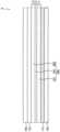
도 1은 본 발명의 예시적인 실시예들에 따른 유기 발광 표시 장치를 나타내는 단면도이다.
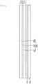
도 2는 도 1의 'A'영역을 확대 도시한 단면도이다.
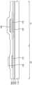
도 3A는 도 1의 'B'영역을 확대 도시한 단면도이다.
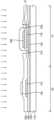
도 3B는 언더 컷 현상을 설명하기 위한 단면도이다.
도 4 내지 도 16은 본 발명의 예시적인 실시예들에 따른 유기 발광 표시 장치의 제조 방법을 나타내는 단면도들이다.FIG. 1 is a cross-sectional view showing an organic light emitting display device according to exemplary embodiments of the present invention.
Figure 2 is an enlarged cross-sectional view of area ‘A’ of Figure 1.
Figure 3A is an enlarged cross-sectional view of area ‘B’ of Figure 1.
Figure 3B is a cross-sectional view to explain the undercut phenomenon.
FIGS. 4 to 16 are cross-sectional views showing a method for manufacturing an organic light-emitting display device according to exemplary embodiments of the present invention.
이하, 첨부한 도면들을 참조하여, 본 발명의 예시적인 실시예들에 따른 유기 발광 표시 장치 및 유기 발광 표시 장치의 제조 방법에 대하여 상세하게 설명한다. 첨부한 도면들에 있어서, 동일하거나 유사한 구성 요소들에 대해서는 동일하거나 유사한 참조 부호들을 사용한다.Hereinafter, with reference to the attached drawings, an organic light emitting display device and a method of manufacturing the organic light emitting display device according to exemplary embodiments of the present invention will be described in detail. In the attached drawings, identical or similar reference numerals are used for identical or similar components.
도 1은 본 발명의 예시적인 실시예들에 따른 유기 발광 표시 장치를 나타내는 단면도이고, 도 2는 도 1의 'A'영역을 확대 도시한 단면도이며, 도 3A는 도 1의 'B'영역을 확대 도시한 단면도이고, 도 3B는 언더 컷 현상을 설명하기 위한 단면도이다.FIG. 1 is a cross-sectional view showing an organic light-emitting display device according to exemplary embodiments of the present invention, FIG. 2 is an enlarged cross-sectional view showing area 'A' of FIG. 1, FIG. 3A is an enlarged cross-sectional view showing area 'B' of FIG. 1, and FIG. 3B is a cross-sectional view for explaining an undercut phenomenon.
도 1 내지 도 3A를 참조하면, 유기 발광 표시 장치(100)는 기판(110), 제1 반도체 소자(250), 제2 반도체 소자(255), 게이트 전극 패턴(180), 게이트 절연층(150), 층간 절연층(190), 절연층 구조물(300), 보호 절연층(400), 평탄화층(270), 발광 구조물(200), 화소 정의막(310) 등을 포함할 수 있다. 여기서, 제1 반도체 소자(250)는 제1 액티브층(130), 제1 게이트 전극(170), 제1 소스 전극(210) 및 제1 드레인 전극(230)을 포함할 수 있고, 제2 반도체 소자(255)는 제2 액티브층(135), 제2 게이트 전극(175), 제2 소스 전극(215) 및 제2 드레인 전극(235)을 포함할 수 있다. 또한, 절연층 구조물(300)은 제1 절연층(301), 제2 절연층(302) 및 제3 절연층(303)을 포함할 수 있고, 발광 구조물(200)은 하부 전극(290), 발광층(330) 및 상부 전극(340)을 포함할 수 있다. 더욱이, 제1 콘택홀(212) 및 제2 콘택홀(232) 각각을 통해 제1 소스 전극(210) 및 제1 드레인 전극(230)이 제1 액티브층(130)에 접속될 수 있다.Referring to FIGS. 1 to 3A, the organic light-emitting display device (100) may include a substrate (110), a first semiconductor element (250), a second semiconductor element (255), a gate electrode pattern (180), a gate insulating layer (150), an interlayer insulating layer (190), an insulating layer structure (300), a protective insulating layer (400), a planarizing layer (270), a light-emitting structure (200), a pixel defining film (310), etc. Here, the first semiconductor element (250) may include a first active layer (130), a first gate electrode (170), a first source electrode (210), and a first drain electrode (230), and the second semiconductor element (255) may include a second active layer (135), a second gate electrode (175), a second source electrode (215), and a second drain electrode (235). In addition, the insulating layer structure (300) may include a first insulating layer (301), a second insulating layer (302), and a third insulating layer (303), and the light-emitting structure (200) may include a lower electrode (290), a light-emitting layer (330), and an upper electrode (340). Furthermore, the first source electrode (210) and the first drain electrode (230) may be connected to the first active layer (130) through the first contact hole (212) and the second contact hole (232), respectively.
유기 발광 표시 장치(100)가 절연층 구조물(300)을 포함함으로써 유기 발광 표시 장치(100)는 제1 콘택홀(212) 및 제2 콘택홀(232)의 프로파일 불량을 방지할 수 있고, 제1 소스 전극(210) 및 제1 드레인 전극(230) 각각이 제1 액티브층(130)에 용이하게 접속될 수 있다.Since the organic light emitting display device (100) includes the insulating layer structure (300), the organic light emitting display device (100) can prevent profile defects of the first contact hole (212) and the second contact hole (232), and each of the first source electrode (210) and the first drain electrode (230) can be easily connected to the first active layer (130).
기판(110)이 제공될 수 있다. 기판(110)은 투명한 또는 불투명한 재료로 구성될 수 있다. 예를 들면, 기판(110)은 석영 기판, 합성 석영(synthetic quartz) 기판, 불화칼슘 기판, 불소가 도핑된 석영(F-doped quartz) 기판, 소다라임(sodalime) 유리 기판, 무알칼리(non-alkali) 유리 기판 등을 포함할 수 있다. 선택적으로, 기판(110)은 연성을 갖는 투명 수지 기판으로 이루어질 수도 있다. 기판(110)으로 이용될 수 있는 투명 수지 기판의 예로는 폴리이미드 기판을 들 수 있다. 이러한 경우, 상기 폴리이미드 기판은 제1 폴리이미드층, 배리어 필름층, 제2 폴리이미드층 등으로 구성될 수 있다. 예를 들면, 상기 폴리이미드 기판은 경질의 유리 기판 상에 제1 폴리이미드층, 배리어 필름층 및 제2 폴리이미드층이 적층된 구성을 가질 수 있다. 상기 폴리이미드 기판의 제2 폴리이미드층 상에 절연층(예를 들어, 버퍼층)을 배치한 후, 상기 절연층 상에 상부 구조물(예를 들어, 제1 반도체 소자(250), 제2 반도체 소자(255), 발광 구조물(200) 등)이 배치될 수 있다. 이러한 상부 구조물의 형성 후, 상기 경질의 유리 기판이 제거될 수 있다. 즉, 상기 폴리이미드 기판은 얇고 플렉서블하기 때문에, 상기 폴리이미드 기판 상에 상기 상부 구조물을 직접 형성하기 어려울 수 있다. 이러한 점을 고려하여, 상기 경질의 유리 기판을 이용하여 상부 구조물을 형성한 다음, 상기 유리 기판을 제거함으로써, 상기 폴리이미드 기판이 기판(110)으로 이용될 수 있다. 예시적인 실시예들에 있어서, 기판(110)은 제1 영역(10) 및 제2 영역(20)을 가질 수 있고, 제1 영역(10)과 제2 영역(20)은 인접하여 위치할 수 있다. 예를 들면, 제1 영역(10)은 구동 트랜지스터가 배치되는 영역일 수 있고, 제2 영역(20)은 스위칭 트랜지스터가 배치되는 영역일 수 있다.A substrate (110) may be provided. The substrate (110) may be composed of a transparent or opaque material. For example, the substrate (110) may include a quartz substrate, a synthetic quartz substrate, a calcium fluoride substrate, a fluorine-doped quartz (F-doped quartz) substrate, a sodalime glass substrate, a non-alkali glass substrate, etc. Optionally, the substrate (110) may be composed of a transparent resin substrate having flexibility. An example of a transparent resin substrate that may be used as the substrate (110) may be a polyimide substrate. In this case, the polyimide substrate may be composed of a first polyimide layer, a barrier film layer, a second polyimide layer, etc. For example, the polyimide substrate may have a configuration in which the first polyimide layer, the barrier film layer, and the second polyimide layer are laminated on a rigid glass substrate. After an insulating layer (e.g., a buffer layer) is disposed on the second polyimide layer of the polyimide substrate, an upper structure (e.g., a first semiconductor element (250), a second semiconductor element (255), a light-emitting structure (200), etc.) may be disposed on the insulating layer. After the formation of the upper structure, the rigid glass substrate may be removed. That is, since the polyimide substrate is thin and flexible, it may be difficult to directly form the upper structure on the polyimide substrate. Considering this point, by forming the upper structure using the rigid glass substrate and then removing the glass substrate, the polyimide substrate may be used as the substrate (110). In exemplary embodiments, the substrate (110) may have a first region (10) and a second region (20), and the first region (10) and the second region (20) may be positioned adjacent to each other. For example, the first region (10) may be a region where a driving transistor is placed, and the second region (20) may be a region where a switching transistor is placed.
기판(110) 상에 버퍼층(도시되지 않음)이 배치될 수도 있다. 상기 버퍼층은 기판(110) 상에 전체적으로 배치될 수 있다. 상기 버퍼층은 기판(110)으로부터 금속 원자들이나 불순물들이 제1 반도체 소자(250), 제2 반도체 소자(255) 및 발광 구조물(200)로 확산되는 현상을 방지할 수 있으며, 액티브층을 형성하기 위한 결정화 공정 동안 열의 전달 속도를 조절하여 실질적으로 균일한 액티브층을 수득하게 할 수 있다. 또한, 상기 버퍼층은 기판(110)의 표면이 균일하지 않을 경우, 기판(110)의 표면의 평탄도를 향상시키는 역할을 수행할 수 있다. 기판(110)의 유형에 따라 기판(110) 상에 두 개 이상의 버퍼층이 제공될 수 있거나 상기 버퍼층이 배치되지 않을 수 있다. 예를 들면, 상기 버퍼층은 유기 물질 또는 무기 물질을 포함할 수 있다.A buffer layer (not shown) may be disposed on the substrate (110). The buffer layer may be disposed entirely on the substrate (110). The buffer layer may prevent metal atoms or impurities from diffusing from the substrate (110) to the first semiconductor element (250), the second semiconductor element (255), and the light-emitting structure (200), and may control the heat transfer rate during the crystallization process for forming the active layer to obtain a substantially uniform active layer. In addition, the buffer layer may play a role in improving the flatness of the surface of the substrate (110) when the surface of the substrate (110) is not uniform. Depending on the type of the substrate (110), two or more buffer layers may be provided on the substrate (110), or the buffer layer may not be disposed. For example, the buffer layer may include an organic material or an inorganic material.
제1 액티브층(130)이 기판(110) 상의 제1 영역(10)에 배치될 수 있다. 예를 들면, 제1 액티브층(130)은 산화물 반도체, 아몰퍼스 실리콘(amorphous silicon), 폴리 실리콘(poly silicon) 또는 유기물 반도체 등을 포함할 수 있다. 예시적인 실시예들에 있어서, 제1 액티브층(130)은 실리콘계 반도체를 포함할 수 있고, 상기 아몰퍼스 실리콘 또는 폴리 실리콘으로 구성될 수 있다.A first active layer (130) may be disposed in a first region (10) on a substrate (110). For example, the first active layer (130) may include an oxide semiconductor, amorphous silicon, poly silicon, or an organic semiconductor. In exemplary embodiments, the first active layer (130) may include a silicon-based semiconductor and may be composed of the amorphous silicon or poly silicon.
기판(110) 및 제1 액티브층(130) 상의 제1 영역(10) 및 제2 영역(20)에는 게이트 절연층(150)이 배치될 수 있다. 게이트 절연층(150)은 기판(110) 상의 제1 영역(10)에 제1 액티브층(130)을 덮을 수 있고, 기판(110) 상에 전체적으로 배치될 수 있다. 예를 들면, 게이트 절연층(150)은 기판(110) 상에서 제1 액티브층(130)을 덮으며, 제1 액티브층(130)의 프로파일을 따라 실질적으로 동일한 두께로 배치될 수 있다. 이와는 달리, 게이트 절연층(150)은 기판(110) 상에서 제1 액티브층(130)을 충분히 덮을 수 있으며, 제1 액티브층(130)의 주위에 단차를 생성시키지 않고 실질적으로 평탄한 상면을 가질 수도 있다. 게이트 절연층(150)은 실리콘 화합물, 금속 산화물 등을 포함할 수 있다. 예를 들면, 게이트 절연층(150)은 실리콘 산화물(SiOx), 실리콘 질화물(SiNx), 실리콘 산질화물(SiOxNy), 실리콘 산탄화물(SiOxCy), 실리콘 탄질화물(SiCxNy), 실리콘 산탄화물(SiOxCy), 알루미늄 산화물(AlOx), 알루미늄 질화물(AlNx), 탄탈륨 산화물(TaOx), 하프늄 산화물(HfOx), 지르코늄 산화물(ZrOx), 티타늄 산화물(TiOx) 등으로 구성될 수 있다.A gate insulating layer (150) may be disposed on the first region (10) and the second region (20) on the substrate (110) and the first active layer (130). The gate insulating layer (150) may cover the first active layer (130) on the first region (10) on the substrate (110) and may be disposed entirely on the substrate (110). For example, the gate insulating layer (150) may cover the first active layer (130) on the substrate (110) and may be disposed with substantially the same thickness along the profile of the first active layer (130). Alternatively, the gate insulating layer (150) may sufficiently cover the first active layer (130) on the substrate (110) and may have a substantially flat upper surface without generating a step around the first active layer (130). The gate insulating layer (150) may include a silicon compound, a metal oxide, or the like. For example, the gate insulating layer (150) may be composed of silicon oxide (SiOx), silicon nitride (SiNx), silicon oxynitride (SiOxNy), silicon oxycarbide (SiOxCy), silicon carbonitride (SiCxNy), silicon oxycarbide (SiOxCy), aluminum oxide (AlOx), aluminum nitride (AlNx), tantalum oxide (TaOx), hafnium oxide (HfOx), zirconium oxide (ZrOx), titanium oxide (TiOx), or the like.
제1 게이트 전극(170)은 게이트 절연층(150) 상의 제1 영역(10)에 배치될 수 있다. 제1 게이트 전극(170)은 게이트 절연층(150) 중에서 하부에 제1 액티브층(130)이 위치하는 부분 상에 배치될 수 있다. 제1 게이트 전극(170)은 금속, 금속 합금, 금속 질화물, 도전성 금속 산화물, 투명 도전성 물질 등을 포함할 수 있다. 예를 들면, 제1 게이트 전극(170)은 금(Au), 은(Ag), 알루미늄(Al), 백금(Pt), 니켈(Ni), 티타늄(Ti), 팔라듐(Pd), 마그네슘(Mg), 칼슘(Ca), 리튬(Li), 크롬(Cr), 탄탈륨(Ta), 몰리브데늄(Mo), 스칸듐(Sc), 네오디뮴(Nd), 이리듐(Ir), 알루미늄을 함유하는 합금, 알루미늄 질화물(AlNx), 은을 함유하는 합금, 텅스텐(W), 텅스텐 질화물(WNx), 구리를 함유하는 합금, 몰리브데늄을 함유하는 합금, 티타늄 질화물(TiNx), 탄탈륨 질화물(TaNx), 스트론튬 루테늄 산화물(SrRuxOy), 아연 산화물(ZnOx), 인듐 주석 산화물(ITO), 주석 산화물(SnOx), 인듐 산화물(InOx), 갈륨 산화물(GaOx), 인듐 아연 산화물(IZO) 등으로 구성될 수 있다. 이들은 단독으로 또는 서로 조합되어 사용될 수 있다. 선택적으로, 제1 게이트 전극(170)은 복수의 층들을 포함하는 다층 구조를 가질 수도 있다.The first gate electrode (170) may be placed in the first region (10) on the gate insulating layer (150). The first gate electrode (170) may be placed on a portion of the gate insulating layer (150) where the first active layer (130) is positioned at the bottom. The first gate electrode (170) may include a metal, a metal alloy, a metal nitride, a conductive metal oxide, a transparent conductive material, or the like. For example, the first gate electrode (170) may be composed of gold (Au), silver (Ag), aluminum (Al), platinum (Pt), nickel (Ni), titanium (Ti), palladium (Pd), magnesium (Mg), calcium (Ca), lithium (Li), chromium (Cr), tantalum (Ta), molybdenum (Mo), scandium (Sc), neodymium (Nd), iridium (Ir), an alloy containing aluminum, aluminum nitride (AlNx), an alloy containing silver, tungsten (W), tungsten nitride (WNx), an alloy containing copper, an alloy containing molybdenum, titanium nitride (TiNx), tantalum nitride (TaNx), strontium ruthenium oxide (SrRuxOy), zinc oxide (ZnOx), indium tin oxide (ITO), tin oxide (SnOx), indium oxide (InOx), gallium oxide (GaOx), indium zinc oxide (IZO), and the like. These may be used alone or in combination with each other. Optionally, the first gate electrode (170) may have a multilayer structure including a plurality of layers.
게이트 절연층(150) 및 제1 게이트 전극(170) 상의 제1 영역(10) 및 제2 영역(20)에는 층간 절연층(190)이 배치될 수 있다. 층간 절연층(190)은 게이트 절연층(150) 상의 제1 영역(10)에서 제1 게이트 전극(170)을 덮을 수 있고, 게이트 절연층(150) 상에 전체적으로 배치될 수 있다. 예를 들면, 층간 절연층(190)은 게이트 절연층(150) 상에서 제1 게이트 전극(170)을 덮으며, 제1 게이트 전극(170)의 프로파일을 따라 실질적으로 동일한 두께로 배치될 수 있다. 이와는 달리, 층간 절연층(190)은 게이트 절연층(150) 상에서 제1 게이트 전극(170)을 충분히 덮을 수 있으며, 제1 게이트 전극(170)의 주위에 단차를 생성시키지 않고 실질적으로 평탄한 상면을 가질 수도 있다. 층간 절연층(190)은 실리콘 화합물, 금속 산화물 등을 포함할 수 있다.An interlayer insulating layer (190) may be disposed in the first region (10) and the second region (20) on the gate insulating layer (150) and the first gate electrode (170). The interlayer insulating layer (190) may cover the first gate electrode (170) in the first region (10) on the gate insulating layer (150) and may be disposed entirely on the gate insulating layer (150). For example, the interlayer insulating layer (190) may cover the first gate electrode (170) on the gate insulating layer (150) and may be disposed with substantially the same thickness along the profile of the first gate electrode (170). Alternatively, the interlayer insulating layer (190) may sufficiently cover the first gate electrode (170) on the gate insulating layer (150) and may have a substantially flat upper surface without generating a step around the first gate electrode (170). The interlayer insulating layer (190) may include a silicon compound, a metal oxide, or the like.
게이트 전극 패턴(180)이 층간 절연층(190) 상의 제1 영역(10)에 배치될 수 있다. 게이트 전극 패턴(180)은 층간 절연층(190) 중에서 하부에 제1 게이트 전극(170)이 위치하는 부분 상에 배치될 수 있다. 게이트 전극 패턴(180)은 배선으로 기능할 수 있다. 예를 들면, 게이트 전극 패턴(180)은 데이터 신호를 제공하는 데이터 신호 배선, 게이트 신호를 제공하는 게이트 신호 배선, 초기화 신호를 제공하는 초기화 신호 배선, 발광 신호를 제공하는 발광 신호 배선, 전압 전압을 제공하는 전원 전압 배선 등일 수 있다. 게이트 전극 패턴(180)은 금속, 금속 합금, 금속 질화물, 도전성 금속 산화물, 투명 도전성 물질 등을 포함할 수 있다.A gate electrode pattern (180) may be arranged in a first region (10) on an interlayer insulating layer (190). The gate electrode pattern (180) may be arranged on a portion of the interlayer insulating layer (190) where the first gate electrode (170) is positioned at a lower portion. The gate electrode pattern (180) may function as a wiring. For example, the gate electrode pattern (180) may be a data signal wiring that provides a data signal, a gate signal wiring that provides a gate signal, an initialization signal wiring that provides an initialization signal, an emission signal wiring that provides an emission signal, a power voltage wiring that provides a voltage, etc. The gate electrode pattern (180) may include a metal, a metal alloy, a metal nitride, a conductive metal oxide, a transparent conductive material, etc.
제2 게이트 전극(175)은 층간 절연층(190) 상의 제2 영역(20)에 배치될 수 있다. 예시적인 실시예들에 있어서, 제2 게이트 전극(175)은 게이트 전극 패턴(180)과 동일한 층에 위치할 수 있고, 동일한 물질을 사용하여 동시에 형성될 수 있다. 제2 게이트 전극(175)은 금속, 금속 합금, 금속 질화물, 도전성 금속 산화물, 투명 도전성 물질 등을 포함할 수 있다.The second gate electrode (175) may be disposed in the second region (20) on the interlayer insulating layer (190). In exemplary embodiments, the second gate electrode (175) may be positioned in the same layer as the gate electrode pattern (180) and may be formed simultaneously using the same material. The second gate electrode (175) may include a metal, a metal alloy, a metal nitride, a conductive metal oxide, a transparent conductive material, or the like.
도 1 및 도 2를 다시 참조하면, 층간 절연층(190), 제2 게이트 전극(175) 및 게이트 전극 패턴(180) 상에 절연층 구조물(300)이 배치될 수 있다. 예시적인 실시예들에 있어서, 절연층 구조물(300)은 제1 영역(10)에서 제1 소스 및 제1 드레인 전극들(210, 230)과 게이트 전극 패턴(180) 사이에 개재될 수 있고, 제2 영역(20)에서 제2 액티브층(135)과 제2 게이트 전극(175) 사이에 개재될 수 있으며, 절연층 구조물(300)은 제1 절연층(301), 제2 절연층(302) 및 제3 절연층(303)을 포함할 수 있다.Referring back to FIGS. 1 and 2, an insulating layer structure (300) may be disposed on the interlayer insulating layer (190), the second gate electrode (175), and the gate electrode pattern (180). In exemplary embodiments, the insulating layer structure (300) may be interposed between the first source and first drain electrodes (210, 230) and the gate electrode pattern (180) in the first region (10), and may be interposed between the second active layer (135) and the second gate electrode (175) in the second region (20), and the insulating layer structure (300) may include a first insulating layer (301), a second insulating layer (302), and a third insulating layer (303).
제1 절연층(301)은 층간 절연층(190) 상의 제1 영역(10)에서 게이트 전극 패턴(180) 및 제2 영역(20)에서 제2 게이트 전극(175)을 덮을 수 있고, 층간 절연층(190) 상에 전체적으로 배치될 수 있다. 예를 들면, 제1 절연층(301)은 층간 절연층(190) 상에서 게이트 전극 패턴(180) 및 제2 게이트 전극(175)을 덮으며, 게이트 전극 패턴(180) 및 제2 게이트 전극(175)의 프로파일을 따라 실질적으로 동일한 두께로 배치될 수 있다. 이와는 달리, 제1 절연층(301)은 층간 절연층(190) 상에서 게이트 전극 패턴(180) 및 제2 게이트 전극(175)을 충분히 덮을 수 있으며, 게이트 전극 패턴(180) 및 제2 게이트 전극(175)의 주위에 단차를 생성시키지 않고 실질적으로 평탄한 상면을 가질 수도 있다. 예시적인 실시예들에 있어서, 제1 절연층(301)은 동일한 식각 공정에 대해 제1 식각률(etching rate)을 가질 수 있다. 여기서, 제1 절연층(301)은 상기 제1 식각률을 갖는 산화물계 절연층을 포함할 수 있다. 예를 들면, 제1 절연층(301)은 실리콘 산화물 또는 알루미늄 산화물로 구성될 수 있다. 또한, 제1 절연층(301)은 제1 두께(T1)를 가질 수 있다.The first insulating layer (301) can cover the gate electrode pattern (180) in the first region (10) on the interlayer insulating layer (190) and the second gate electrode (175) in the second region (20), and can be disposed entirely on the interlayer insulating layer (190). For example, the first insulating layer (301) can cover the gate electrode pattern (180) and the second gate electrode (175) on the interlayer insulating layer (190), and can be disposed with substantially the same thickness along the profiles of the gate electrode pattern (180) and the second gate electrode (175). Alternatively, the first insulating layer (301) can sufficiently cover the gate electrode pattern (180) and the second gate electrode (175) on the interlayer insulating layer (190), and can have a substantially flat upper surface without generating a step around the gate electrode pattern (180) and the second gate electrode (175). In exemplary embodiments, the first insulating layer (301) may have a first etching rate for the same etching process. Here, the first insulating layer (301) may include an oxide-based insulating layer having the first etching rate. For example, the first insulating layer (301) may be composed of silicon oxide or aluminum oxide. In addition, the first insulating layer (301) may have a first thickness (T1).
제1 절연층(301) 상에 제2 절연층(302)이 배치될 수 있다. 제2 절연층(302)은 제1 절연층(301) 상에 전체적으로 배치될 수 있다. 예를 들면, 제2 절연층(302)은 제1 절연층(301)의 프로파일을 따라 실질적으로 동일한 두께로 배치될 수 있다. 이와는 달리, 제2 절연층(302)은 제1 절연층(301)을 충분히 덮을 수 있으며, 실질적으로 평탄한 상면을 가질 수도 있다.A second insulating layer (302) may be disposed on the first insulating layer (301). The second insulating layer (302) may be disposed entirely on the first insulating layer (301). For example, the second insulating layer (302) may be disposed with substantially the same thickness along the profile of the first insulating layer (301). Alternatively, the second insulating layer (302) may sufficiently cover the first insulating layer (301) and may have a substantially flat upper surface.
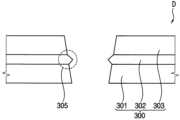
제2 절연층(302)은 제2 액티브층(135)의 과잉 산소 결함을 방지할 수 있고, 제1 액티브층(130)의 실리콘 불포화 결합(dangling bond) 결함을 방지할 수 있다. 예시적인 실시예들에 있어서, 제2 절연층(302)은 동일한 식각 공정에 대해 상기 제1 식각률보다 높은 제2 식각률을 가질 수 있다. 예를 들면, 동일한 식각 공정에서 제2 절연층(302)이 제1 절연층(301)보다 빨리 식각될 수 있다. 다시 말하면, 동일한 식각 공정에서 제2 절연층(302)이 제1 절연층(301)보다 더 많이 식각될 수 있다. 여기서, 제2 절연층(302)은 상기 제2 식각률을 갖는 질화물계 절연층을 포함할 수 있다. 예를 들면, 제2 절연층(302)은 실리콘 질화물 또는 티타늄 질화물로 구성될 수 있다. 또한, 제2 절연층(302)은 제1 두께(T1)보다 작은 제2 두께(T2)를 가질 수 있다. 더욱이, 도 3A에 도시된 바와 같이, 제2 절연층(302)은 제1 콘택홀(212) 및 제2 콘택홀(232)이 위치하는 부분에서 상기 콘택홀의 내측으로 돌출되는 돌출부(305)를 가질 수 있다.The second insulating layer (302) can prevent excessive oxygen defects in the second active layer (135) and can prevent silicon dangling bond defects in the first active layer (130). In exemplary embodiments, the second insulating layer (302) can have a second etching rate higher than the first etching rate for the same etching process. For example, the second insulating layer (302) can be etched faster than the first insulating layer (301) in the same etching process. In other words, the second insulating layer (302) can be etched more than the first insulating layer (301) in the same etching process. Here, the second insulating layer (302) can include a nitride-based insulating layer having the second etching rate. For example, the second insulating layer (302) can be composed of silicon nitride or titanium nitride. In addition, the second insulating layer (302) may have a second thickness (T2) smaller than the first thickness (T1). Furthermore, as illustrated in FIG. 3A, the second insulating layer (302) may have a protrusion (305) protruding inwardly from the first contact hole (212) and the second contact hole (232) at a portion where the first contact hole (212) and the second contact hole (232) are located.
제2 절연층(302) 상에 제3 절연층(303)이 배치될 수 있다. 제3 절연층(303)은 제2 절연층(302) 상에 전체적으로 배치될 수 있다. 예를 들면, 제3 절연층(303)은 제2 절연층(302)의 프로파일을 따라 실질적으로 동일한 두께로 배치될 수 있다. 이와는 달리, 제3 절연층(303)은 제2 절연층(302)을 충분히 덮을 수 있으며, 실질적으로 평탄한 상면을 가질 수도 있다. 예시적인 실시예들에 있어서, 제3 절연층(303)은 동일한 식각 공정에 대해 상기 제2 식각률보다 낮은 제3 식각률을 가질 수 있다. 여기서, 제3 절연층(303)은 상기 제3 식각률을 갖는 산화물계 절연층을 포함할 수 있다. 예를 들면, 제3 절연층(303)은 실리콘 산화물 또는 알루미늄 산화물로 구성될 수 있다. 또한, 제3 절연층(303)은 제3 두께(T3)를 가질 수 있다. 제1 절연층(301) 및 제3 절연층(303)은 동일한 물질을 포함할 수 있고, 제1 두께(T1)와 제3 두께(T3)는 실질적으로 동일할 수 있으며, 상기 제1 식각률과 상기 제3 식각률은 실질적으로 동일할 수 있다. 또한, 제2 두께(T2)는 절연층 구조물(300)의 두께의 30% 미만일 수 있다. 선택적으로, 제1 두께(T1)와 제3 두께(T3)는 다를 수 있고, 상기 제1 식각률과 상기 제3 식각률이 다를 수 있지만, 제1 및 제3 두께(T1, T3)는 제2 두께(T2)보다 크고, 상기 제3 식각률은 상기 제2 식각률보다 작아야 한다. 이와 같이, 제1 절연층(301), 제2 절연층(302) 및 제3 절연층(303)을 포함하는 절연층 구조물(300)이 구성될 수 있다.A third insulating layer (303) may be disposed on the second insulating layer (302). The third insulating layer (303) may be disposed entirely on the second insulating layer (302). For example, the third insulating layer (303) may be disposed with substantially the same thickness along the profile of the second insulating layer (302). Alternatively, the third insulating layer (303) may sufficiently cover the second insulating layer (302) and may have a substantially flat upper surface. In exemplary embodiments, the third insulating layer (303) may have a third etching rate lower than the second etching rate for the same etching process. Here, the third insulating layer (303) may include an oxide-based insulating layer having the third etching rate. For example, the third insulating layer (303) may be composed of silicon oxide or aluminum oxide. In addition, the third insulating layer (303) may have a third thickness (T3). The first insulating layer (301) and the third insulating layer (303) may include the same material, and the first thickness (T1) and the third thickness (T3) may be substantially the same, and the first etching rate and the third etching rate may be substantially the same. In addition, the second thickness (T2) may be less than 30% of the thickness of the insulating layer structure (300). Optionally, the first thickness (T1) and the third thickness (T3) may be different, and the first etching rate and the third etching rate may be different, but the first and third thicknesses (T1, T3) should be greater than the second thickness (T2), and the third etching rate should be less than the second etching rate. In this way, an insulating layer structure (300) including the first insulating layer (301), the second insulating layer (302), and the third insulating layer (303) can be configured.
다만, 절연층 구조물(300)이 3개의 층들(예를 들어, 제1 절연층(301), 제2 절연층(302) 및 제3 절연층(303))을 포함하는 구성을 갖는 것으로 설명하였으나, 본 발명의 구성이 이에 한정되는 것은 아니다. 예를 들면, 절연층 구조물(300)은 적어도 4개의 층들을 갖는 구조를 가질 수도 있다.However, although the insulation layer structure (300) has been described as having a configuration including three layers (e.g., a first insulation layer (301), a second insulation layer (302), and a third insulation layer (303)), the configuration of the present invention is not limited thereto. For example, the insulation layer structure (300) may have a structure having at least four layers.
예시적인 실시예들에 있어서, 제2 반도체 소자(255)의 특성 확보를 위해 또는 신뢰성을 확보하기 위해 제3 절연층(303)은 제2 액티브층(135)과 직접적으로 접촉할 수 있다. 다시 말하면, 제3 절연층(303)의 상면은 제2 액티브층(135)의 저면과 직접적으로 접촉할 수 있고, 제3 절연층(303)의 저면은 제2 절연층(302)의 상면과 직접적으로 접촉할 수 있다. 예를 들면, 산화물 반도체로 구성된 제2 액티브층(135)과 실리콘 산화물로 구성된 제3 절연층(303)이 직접적으로 접촉하는 경우 제2 액티브층(135)의 계면 특성이 상대적으로 개선될 수 있다.In exemplary embodiments, in order to secure the characteristics of the second semiconductor element (255) or to secure reliability, the third insulating layer (303) may be in direct contact with the second active layer (135). In other words, the upper surface of the third insulating layer (303) may be in direct contact with the lower surface of the second active layer (135), and the lower surface of the third insulating layer (303) may be in direct contact with the upper surface of the second insulating layer (302). For example, when the second active layer (135) composed of an oxide semiconductor and the third insulating layer (303) composed of silicon oxide are in direct contact, the interface characteristics of the second active layer (135) may be relatively improved.
또한, 제1 콘택홀(212) 및 제2 콘택홀(232)이 형성되는 과정에서 BOE(buffered oxide etchant) 공정이 진행되는 동안 제1 영역(10)에 위치한 제1 콘택홀(212) 및 제2 콘택홀(232) 각각의 측벽의 일부가 제거될 수 있다. 예를 들면, 제1 및 제2 콘택홀들(212, 232)에 열처리 공정을 수행한 후 상기 BOE 공정을 진행하는 경우, 제1 콘택홀(212) 및 제2 콘택홀(232)에 위치하는 절연층 구조물(300)의 측벽에 언더 컷(under cut) 현상이 발생되지 않도록 절연층 구조물(300)은 상기 제2 식각률을 갖는 제2 절연층(302) 아래에 배치되는 상기 제1 식각률을 갖는 제1 절연층(301)을 포함할 수 있다.In addition, during the process of forming the first contact hole (212) and the second contact hole (232), a portion of the sidewall of each of the first contact hole (212) and the second contact hole (232) located in the first region (10) may be removed while the BOE (buffered oxide etchant) process is performed. For example, when the BOE process is performed after performing a heat treatment process on the first and second contact holes (212, 232), the insulating layer structure (300) located in the first contact hole (212) and the second contact hole (232) may include a first insulating layer (301) having the first etching rate, which is arranged below a second insulating layer (302) having the second etching rate, so that an undercut phenomenon does not occur on the sidewall of the insulating layer structure (300).
예를 들면, 도 3B에 도시된 바와 같이, 종래의 절연층 구조물이 실리콘 산화물을 포함하는 제3 절연층(1303) 및 실리콘 질화물을 포함하는 제2 절연층(1302)으로 구성되는 경우, 상기 BOE 공정의 에천트에 의해 상기 제1 및 제2 콘택홀들에 위치하는 상기 제2 절연층(1302)의 측벽에서 언더 컷 현상이 발생될 수 있다. 여기서, 제2 절연층(1302)에 포함된 상기 실리콘 질화물의 N/Si의 조성비가 대략 0.5와 대략 1 사이의 범위를 가질 수 있고, 상기 실리콘 질화물의 두께는 대략 200 나노미터이다. 다시 말하면, 실리콘 질화물은 실리콘 산화물보다 동일한 식각 공정에 대해 상대적으로 높은 식각률을 가질 수 있다. 이러한 경우, 상기 제1 및 제2 콘택홀들에 위치하는 상기 제2 절연층(1302)이 상기 제3 절연층(1303)보다 상대적으로 빠르게 식각되기 때문에 제2 절연층(1302)의 측면 침식이 발생될 수 있고, 상기 제1 및 제2 콘택홀의 프로파일 불량이 발생되거나 콘택 저항이 증가될 수 있다. 즉, 상기 측면 침식이 발생되는 경우, 상기 제3 절연층(1303)의 콘택홀의 폭보다 상기 제2 절연층(1302)의 콘택홀의 폭이 더 큰 형상(예를 들어, 하부가 확장된 콘택홀의 형상)을 갖는 상기 언더 컷 현상이 발생될 수 있다.For example, as illustrated in FIG. 3B, when a conventional insulating layer structure is composed of a third insulating layer (1303) including silicon oxide and a second insulating layer (1302) including silicon nitride, an undercut phenomenon may occur on a sidewall of the second insulating layer (1302) positioned in the first and second contact holes due to the etchant of the BOE process. Here, the composition ratio of N/Si of the silicon nitride included in the second insulating layer (1302) may have a range between about 0.5 and about 1, and the thickness of the silicon nitride is about 200 nanometers. In other words, silicon nitride may have a relatively higher etching rate than silicon oxide for the same etching process. In this case, since the second insulating layer (1302) positioned in the first and second contact holes is etched relatively faster than the third insulating layer (1303), lateral erosion of the second insulating layer (1302) may occur, and a profile defect of the first and second contact holes may occur or contact resistance may increase. That is, when the lateral erosion occurs, the undercut phenomenon may occur in which the width of the contact hole of the second insulating layer (1302) is larger than the width of the contact hole of the third insulating layer (1303) (for example, the shape of a contact hole with an expanded lower portion).
예시적인 실시예들에 있어서, 제2 절연층(302)의 N/Si의 조성비가 대략 1과 대략 2 사이의 범위를 가질 수 있고, 상기 실리콘 질화물의 두께는 대략 100 나노미터이다. 여기서, 제2 절연층(302)의 N의 비율이 상대적으로 높고, 막질이 치밀할 수 있다. 이에 따라, 제2 절연층(302)의 식각률이 상대적으로 느려져 제2 절연층(302)은 돌출부(305)를 가질 수 있다. 또한, 돌출부(305)를 작게 생성되도록 제2 절연층(302)은 상대적으로 작은 두께를 가질 수 있다.In exemplary embodiments, the composition ratio of N/Si of the second insulating layer (302) may range from about 1 to about 2, and the thickness of the silicon nitride may be about 100 nanometers. Here, the ratio of N of the second insulating layer (302) may be relatively high, and the film may be dense. Accordingly, the etching rate of the second insulating layer (302) may be relatively slow, so that the second insulating layer (302) may have a protrusion (305). In addition, the second insulating layer (302) may have a relatively small thickness so that the protrusion (305) is created small.
예시적인 실시예들에 따른 유기 발광 표시 장치(100)는 동일 식각 공정에 대해 상기 제2 식각률을 갖는 제2 절연층(302) 아래에 상기 제2 식각률보다 작은 상기 제1 식각률을 갖는 제1 절연층(301)을 포함함으로써 상기BOE 공정에서 제1 및 제2 콘택홀들(212, 232)에 위치하는 제1 절연층(301)이 제2 절연층(302)보다 상대적으로 느리게 식각되기 때문에 상기 BOE 공정에서 사용되는 에천트에 의한 상기 언더 컷 현상을 방지할 수 있다. 제1 절연층(301)과 제2 절연층(302)의 식각률 차이 때문에 제1 및 제2 콘택홀들(212, 232)에 위치하는 제2 절연층(302)에 돌출부(305)가 형성될 수 있다. 예시적인 실시예들에 있어서, 돌출부(305)의 크기가 상대적으로 크게 형성되지 않도록 제2 절연층(302)의 제2 두께(T2)는 제1 두께(T1) 및 제3 두께(T3)보다 상대적으로 작은 두께를 가질 수 있다. 예를 들면, 제2 절연층(302)의 두께가 상대적으로 두껍게 형성되는 경우, 돌출부(305)의 크기가 상대적으로 크게 형성될 수 있다. 이러한 경우, 제1 소스 전극(210) 및 제1 드레인 전극(230)이 제1 액티브층(130)에 접속되지 않을 수 있거나 콘택 저항이 증가될 수 있다. 따라서, 제2 절연층(302)의 두께는 절연층 구조물(300)의 두께의 30% 미만으로 형성될 수 있다.The organic light emitting display device (100) according to exemplary embodiments includes a first insulating layer (301) having a first etching rate lower than the second etching rate under a second insulating layer (302) having the second etching rate for the same etching process, so that the first insulating layer (301) positioned in the first and second contact holes (212, 232) in the BOE process is etched relatively more slowly than the second insulating layer (302), thereby preventing the undercut phenomenon caused by the etchant used in the BOE process. Due to the difference in etching rates between the first insulating layer (301) and the second insulating layer (302), a protrusion (305) may be formed in the second insulating layer (302) positioned in the first and second contact holes (212, 232). In exemplary embodiments, the second thickness (T2) of the second insulating layer (302) may have a relatively smaller thickness than the first thickness (T1) and the third thickness (T3) so that the size of the protrusion (305) is not formed relatively large. For example, when the thickness of the second insulating layer (302) is formed relatively thick, the size of the protrusion (305) may be formed relatively large. In this case, the first source electrode (210) and the first drain electrode (230) may not be connected to the first active layer (130) or the contact resistance may increase. Therefore, the thickness of the second insulating layer (302) may be formed to be less than 30% of the thickness of the insulating layer structure (300).
제1 소스 전극(210) 및 제1 드레인 전극(230)이 절연층 구조물(300) 상의 제1 영역(10)에 배치될 수 있다. 제1 소스 전극(210)은 절연층 구조물(300), 층간 절연층(190) 및 게이트 절연층(150)의 제1 부분을 제거하여 형성된 제1 콘택홀(212)을 통해 제1 액티브층(130)의 소스 영역에 접속될 수 있고, 제1 드레인 전극(230)은 절연층 구조물(300), 층간 절연층(190) 및 게이트 절연층(150)의 제2 부분을 제거하여 형성된 제2 콘택홀(232)을 통해 제1 액티브층(130)의 드레인 영역에 접속될 수 있다. 도 3A에 도시된 바와 같이, 제2 절연층(302)의 돌출부(305) 때문에 제1 소스 전극(210) 및 제1 드레인 전극(230) 각각은 돌출부(305)와 인접하여 리세스를 가질 수 있다. 제1 소스 전극(210) 및 제1 드레인 전극(230) 각각은 금속, 합금, 금속 질화물, 도전성 금속 산화물, 투명 도전성 물질 등을 포함할 수 있다. 이들은 단독으로 또는 서로 조합되어 사용될 수 있다. 다른 예시적인 실시예들에 있어서, 제1 소스 전극(210) 및 제1 드레인 전극(230) 각각은 복수의 층들을 포함하는 다층 구조를 가질 수도 있다. 이에 따라, 제1 액티브층(130), 제1 게이트 전극(170), 제1 소스 전극(210) 및 제1 드레인 전극(230)을 포함하는 제1 반도체 소자(250)가 구성될 수 있다. 여기서, 제1 반도체 소자(250)는 실리콘계 반도체를 포함하는 구동 트랜지스터로 기능할 수 있다. 또한, 제1 반도체 소자(250)는 상부 게이트 구조를 갖는 트랜지스터로 기능할 수 있다.A first source electrode (210) and a first drain electrode (230) may be arranged in a first region (10) on an insulating layer structure (300). The first source electrode (210) may be connected to a source region of the first active layer (130) through a first contact hole (212) formed by removing a first portion of the insulating layer structure (300), the interlayer insulating layer (190), and the gate insulating layer (150), and the first drain electrode (230) may be connected to a drain region of the first active layer (130) through a second contact hole (232) formed by removing a second portion of the insulating layer structure (300), the interlayer insulating layer (190), and the gate insulating layer (150). As illustrated in FIG. 3A, each of the first source electrode (210) and the first drain electrode (230) may have a recess adjacent to the protrusion (305) due to the protrusion (305) of the second insulating layer (302). Each of the first source electrode (210) and the first drain electrode (230) may include a metal, an alloy, a metal nitride, a conductive metal oxide, a transparent conductive material, or the like. These may be used alone or in combination with each other. In other exemplary embodiments, each of the first source electrode (210) and the first drain electrode (230) may have a multilayer structure including a plurality of layers. Accordingly, a first semiconductor element (250) including a first active layer (130), a first gate electrode (170), a first source electrode (210), and a first drain electrode (230) may be configured. Here, the first semiconductor element (250) may function as a driving transistor including a silicon-based semiconductor. Additionally, the first semiconductor element (250) can function as a transistor having an upper gate structure.
제2 액티브층(135)이 절연층 구조물(300) 상의 제2 영역(20)에 배치될 수 있다. 제2 액티브층(135)은 절연층 구조물(300) 중에서 하부에 제2 게이트 전극(175)이 위치하는 부분 상에 배치될 수 있다. 제2 액티브층(135)은 산화물 반도체를 포함할 수 있다. 다시 말하면, 제2 액티브층(135)은 인듐(In), 아연(Zn), 갈륨(Ga), 주석(Sn), 티타늄(Ti), 알루미늄(Al), 하프늄(Hf), 지르코늄(Zr), 마그네슘(Mg) 등을 함유하는 이성분계 화합물(ABx), 삼성분계 화합물(ABxCy), 사성분계 화합물(ABxCyDz) 등을 포함하는 산화물 반도체층일 수 있다. 예를 들면, 제2 액티브층(135)은 아연 산화물(ZnOx), 갈륨 산화물(GaOx), 티타늄 산화물(TiOx), 주석 산화물(SnOx), 인듐 산화물(InOx), 인듐-갈륨 산화물(IGO), 인듐-아연 산화물(IZO), 인듐-주석 산화물(ITO), 갈륨-아연 산화물(GZO), 아연-마그네슘 산화물(ZMO), 아연-주석 산화물(ZTO), 아연-지르코늄 산화물(ZnZrxOy), 인듐-갈륨-아연 산화물(IGZO), 인듐-아연-주석 산화물(IZTO), 인듐-갈륨-하프늄 산화물(IGHO), 주석-알루미늄-아연 산화물(TAZO) 및 인듐-갈륨-주석 산화물(IGTO) 등을 포함할 수 있다.A second active layer (135) may be disposed in a second region (20) on an insulating layer structure (300). The second active layer (135) may be disposed on a portion of the insulating layer structure (300) at a lower portion of the second gate electrode (175). The second active layer (135) may include an oxide semiconductor. In other words, the second active layer (135) may be an oxide semiconductor layer including a binary compound (ABx), a ternary compound (ABxCy), a quaternary compound (ABxCyDz), or the like, containing indium (In), zinc (Zn), gallium (Ga), tin (Sn), titanium (Ti), aluminum (Al), hafnium (Hf), zirconium (Zr), magnesium (Mg), or the like. For example, the second active layer (135) may include zinc oxide (ZnOx), gallium oxide (GaOx), titanium oxide (TiOx), tin oxide (SnOx), indium oxide (InOx), indium-gallium oxide (IGO), indium-zinc oxide (IZO), indium-tin oxide (ITO), gallium-zinc oxide (GZO), zinc-magnesium oxide (ZMO), zinc-tin oxide (ZTO), zinc-zirconium oxide (ZnZrxOy), indium-gallium-zinc oxide (IGZO), indium-zinc-tin oxide (IZTO), indium-gallium-hafnium oxide (IGHO), tin-aluminum-zinc oxide (TAZO), and indium-gallium-tin oxide (IGTO).
제2 소스 전극(215) 및 제2 드레인 전극(235)이 절연층 구조물(300) 상의 제2 영역(20)에 배치될 수 있다. 제2 소스 전극(215)은 제2 액티브층(135)의 제1 측부를 커버할 수 있고, 제2 드레인 전극(235)은 제2 액티브층(135)의 상기 제1 측부와 다른 제2 측부를 커버할 수 있다. 다시 말하면, 제2 소스 및 제2 드레인 전극들(215, 235)은 제2 액티브층(135)의 양측부를 커버할 수 있고, 제2 액티브층(135)의 상면의 일부를 노출시킬 수 있다. 제2 소스 전극(215) 및 제2 드레인 전극(235) 각각은 금속, 합금, 금속 질화물, 도전성 금속 산화물, 투명 도전성 물질 등을 포함할 수 있다. 이들은 단독으로 또는 서로 조합되어 사용될 수 있다. 예시적인 실시예들에 있어서, 제1 소스 및 제1 드레인 전극들(210, 230) 및 제2 소스 및 제2 드레인 전극들(215, 235)은 동일한 층에 위치할 수 있고, 동일한 물질을 사용하여 동시에 형성될 수 있다. 다른 예시적인 실시예들에 있어서, 제2 소스 전극(215) 및 제2 드레인 전극(235) 각각은 복수의 층들을 포함하는 다층 구조를 가질 수도 있다. 이에 따라, 제2 액티브층(135), 제2 게이트 전극(175), 제2 소스 전극(215) 및 제2 드레인 전극(235)을 포함하는 제2 반도체 소자(255)가 구성될 수 있다. 여기서, 제2 반도체 소자(255)는 산화물계 반도체를 포함하는 스위칭 트랜지스터로 기능할 수 있다. 또한, 제2 반도체 소자(255)는 하부 게이트 구조를 갖는 트랜지스터로 기능할 수 있다.A second source electrode (215) and a second drain electrode (235) may be arranged in a second region (20) on an insulating layer structure (300). The second source electrode (215) may cover a first side of the second active layer (135), and the second drain electrode (235) may cover a second side of the second active layer (135) that is different from the first side. In other words, the second source and second drain electrodes (215, 235) may cover both sides of the second active layer (135) and expose a part of an upper surface of the second active layer (135). Each of the second source electrode (215) and the second drain electrode (235) may include a metal, an alloy, a metal nitride, a conductive metal oxide, a transparent conductive material, or the like. These may be used alone or in combination with each other. In exemplary embodiments, the first source and first drain electrodes (210, 230) and the second source and second drain electrodes (215, 235) may be positioned in the same layer and may be formed simultaneously using the same material. In other exemplary embodiments, each of the second source electrode (215) and the second drain electrode (235) may have a multilayer structure including a plurality of layers. Accordingly, a second semiconductor element (255) including a second active layer (135), a second gate electrode (175), a second source electrode (215), and a second drain electrode (235) may be configured. Here, the second semiconductor element (255) may function as a switching transistor including an oxide-based semiconductor. In addition, the second semiconductor element (255) may function as a transistor having a bottom gate structure.
다만, 유기 발광 표시 장치(100)가 2개의 트랜지스터들(예를 들어, 제1 반도체 소자(250) 및 제2 반도체 소자(255))을 포함하는 구성을 갖는 것으로 설명하였으나, 본 발명의 구성이 이에 한정되는 것은 아니다. 예를 들면, 유기 발광 표시 장치(100)는 적어도 3개의 트랜지스터들 및 적어도 하나의 커패시터를 포함하는 구성을 가질 수도 있다.However, although the organic light-emitting display device (100) has been described as having a configuration including two transistors (e.g., a first semiconductor element (250) and a second semiconductor element (255)), the configuration of the present invention is not limited thereto. For example, the organic light-emitting display device (100) may have a configuration including at least three transistors and at least one capacitor.
절연층 구조물(300), 제1 소스 및 제1 드레인 전극들(210, 230) 및 제2 소스 및 제2 드레인 전극들(215, 235) 상에 보호 절연층(400)이 배치될 수 있다. 보호 절연층(400)은 절연층 구조물(300) 상의 제1 영역(10)에서 제1 소스 및 제1 드레인 전극들(210, 230) 및 제2 영역(20)에서 제2 소스 및 제2 드레인 전극들(215, 235)을 덮을 수 있고, 절연층 구조물(300) 상에 전체적으로 배치될 수 있다. 예를 들면, 보호 절연층(400)은 절연층 구조물(300) 상에서 제1 소스 및 제1 드레인 전극들(210, 230) 및 제2 소스 및 제2 드레인 전극들(215, 235)을 덮으며, 제1 소스 및 제1 드레인 전극들(210, 230) 및 제2 소스 및 제2 드레인 전극들(215, 235)의 프로파일을 따라 실질적으로 동일한 두께로 배치될 수 있다. 이와는 달리, 보호 절연층(400)은 절연층 구조물(300) 상에서 제1 소스 및 제1 드레인 전극들(210, 230) 및 제2 소스 및 제2 드레인 전극들(215, 235)을 충분히 덮을 수 있으며, 제1 소스 및 제1 드레인 전극들(210, 230) 및 제2 소스 및 제2 드레인 전극들(215, 235)의 주위에 단차를 생성시키지 않고 실질적으로 평탄한 상면을 가질 수 있다. 예시적인 실시예들에 있어서, 보호 절연층(400)은 제1 영역(10)에서 제1 드레인 전극(230)의 상면의 일부를 노출시키는 개구(402)를 가질 수 있다. 하부 전극(290)이 개구(402) 및 평탄화층(270)의 콘택홀을 통해 제1 드레인 전극(230)에 접속될 수 있다. 보호 절연층(400)은 실리콘 화합물, 금속 산화물 등을 포함할 수 있다. 예시적인 실시예들에 있어서, 보호 절연층(400)은 실리콘 산화물로 구성될 수 있다. 또한, 보호 절연층(400)은 제2 액티브층(135)의 상면과 직접적으로 접촉할 수 있다. 실리콘 산화물로 구성된 보호 절연층(400)이 제2 액티브층(135)과 직접적으로 접촉함으로써 제2 액티브층(135)의 계면 특성이 상대적으로 개선될 수 있다.A protective insulating layer (400) may be disposed on the insulating layer structure (300), the first source and first drain electrodes (210, 230), and the second source and second drain electrodes (215, 235). The protective insulating layer (400) may cover the first source and first drain electrodes (210, 230) in the first region (10) on the insulating layer structure (300) and the second source and second drain electrodes (215, 235) in the second region (20), and may be disposed entirely on the insulating layer structure (300). For example, the protective insulating layer (400) covers the first source and first drain electrodes (210, 230) and the second source and second drain electrodes (215, 235) on the insulating layer structure (300), and can be arranged with substantially the same thickness along the profiles of the first source and first drain electrodes (210, 230) and the second source and second drain electrodes (215, 235). In contrast, the protective insulating layer (400) can sufficiently cover the first source and first drain electrodes (210, 230) and the second source and second drain electrodes (215, 235) on the insulating layer structure (300) and can have a substantially flat upper surface without creating a step around the first source and first drain electrodes (210, 230) and the second source and second drain electrodes (215, 235). In exemplary embodiments, the protective insulating layer (400) can have an opening (402) exposing a part of the upper surface of the first drain electrode (230) in the first region (10). The lower electrode (290) can be connected to the first drain electrode (230) through the opening (402) and the contact hole of the planarization layer (270). The protective insulating layer (400) may include a silicon compound, a metal oxide, etc. In exemplary embodiments, the protective insulating layer (400) may be composed of silicon oxide. In addition, the protective insulating layer (400) may be in direct contact with the upper surface of the second active layer (135). Since the protective insulating layer (400) composed of silicon oxide is in direct contact with the second active layer (135), the interface characteristics of the second active layer (135) may be relatively improved.
보호 절연층(400) 상에 평탄화층(270)이 배치될 수 있다. 평탄화층(270)은 보호 절연층(400) 상에 전체적으로 배치될 수 있다. 예를 들면, 평탄화층(270)은 보호 절연층(400)을 충분히 덮도록 상대적으로 두꺼운 두께로 배치될 수 있고, 이러한 경우, 평탄화층(270)은 실질적으로 평탄한 상면을 가질 수 있으며, 이와 같은 평탄화층(270)의 평탄한 상면을 구현하기 위하여 평탄화층(270)에 대해 평탄화 공정이 추가될 수 있다. 평탄화층(270)의 일부를 제거하여 형성된 콘택홀을 통해 제1 드레인 전극(230)의 상면의 일부가 노출될 수 있다. 평탄화층(270)은 유기 물질 또는 무기 물질 등을 포함할 수 있다. 예시적인 실시예들에 있어서, 평탄화층(270)은 유기 물질을 포함할 수 있다. 예를 들면, 평탄화층(270)은 포토레지스트, 폴리아크릴계 수지, 폴리이미드계 수지, 폴리아미드계 수지, 실롯산계 수지, 아크릴계 수지, 에폭시계 수지 등으로 구성될 수 있다.A planarization layer (270) may be disposed on the protective insulation layer (400). The planarization layer (270) may be disposed entirely on the protective insulation layer (400). For example, the planarization layer (270) may be disposed with a relatively thick thickness so as to sufficiently cover the protective insulation layer (400), and in this case, the planarization layer (270) may have a substantially flat upper surface, and a planarization process may be added to the planarization layer (270) to implement such a flat upper surface of the planarization layer (270). A part of the upper surface of the first drain electrode (230) may be exposed through a contact hole formed by removing a part of the planarization layer (270). The planarization layer (270) may include an organic material or an inorganic material. In exemplary embodiments, the planarization layer (270) may include an organic material. For example, the flattening layer (270) may be composed of a photoresist, a polyacrylic resin, a polyimide resin, a polyamide resin, a siloxane resin, an acrylic resin, an epoxy resin, etc.
하부 전극(290)은 평탄화층(270) 상에 배치될 수 있다. 하부 전극(290)은 평탄화층(270)의 콘택홀을 관통하여 제1 드레인 전극(230)과 접속할 수 있다. 또한, 하부 전극(290)은 제1 반도체 소자(250)와 전기적으로 연결될 수 있다. 하부 전극(290) 금속, 합금, 금속 질화물, 도전성 금속 산화물, 투명 도전성 물질 등을 포함할 수 있다. 이들은 단독으로 또는 서로 조합되어 사용될 수 있다. 선택적으로, 하부 전극(290)은 복수의 층들을 포함하는 다층 구조를 가질 수도 있다.The lower electrode (290) may be disposed on the planarization layer (270). The lower electrode (290) may be connected to the first drain electrode (230) by penetrating the contact hole of the planarization layer (270). In addition, the lower electrode (290) may be electrically connected to the first semiconductor element (250). The lower electrode (290) may include a metal, an alloy, a metal nitride, a conductive metal oxide, a transparent conductive material, or the like. These may be used alone or in combination with each other. Optionally, the lower electrode (290) may have a multilayer structure including a plurality of layers.
화소 정의막(310)은 하부 전극(290)의 일부 및 평탄화층(270) 상에 배치될 수 있다. 화소 정의막(310)은 하부 전극(290)의 양측부를 덮을 수 있고, 하부 전극(290)의 상면의 일부를 노출시킬 수 있다. 화소 정의막(310)은 유기 물질 또는 무기 물질로 이루어질 수 있다. 예시적인 실시예들에 있어서, 화소 정의막(310)은 유기 물질을 포함할 수 있다.The pixel defining film (310) may be disposed on a portion of the lower electrode (290) and the planarization layer (270). The pixel defining film (310) may cover both sides of the lower electrode (290) and expose a portion of the upper surface of the lower electrode (290). The pixel defining film (310) may be made of an organic material or an inorganic material. In exemplary embodiments, the pixel defining film (310) may include an organic material.
발광층(330)은 화소 정의막(310)에 의해 노출된 하부 전극(290) 상에 배치될 수 있다. 발광층(330)은 서브 화소들에 따라 상이한 색광들(즉, 적색광, 녹색광, 청색광 등)을 방출시킬 수 있는 발광 물질들 중 적어도 하나를 사용하여 형성될 수 있다. 이와는 달리, 발광층(330)은 적색광, 녹색광, 청색광 등의 다른 색광들을 발생시킬 수 있는 복수의 발광 물질들을 적층하여 전체적으로 백색광을 방출할 수 있다. 이러한 경우, 발광층(330) 상에 컬러 필터가 배치(예를 들어, 봉지 기판(미도시)의 저면에 발광층(330)과 중첩되도록 배치)될 수도 있다. 상기 컬러 필터는 적색 컬러 필터, 녹색 컬러 필터, 청색 컬러 필터 중 적어도 하나를 포함할 수 있다. 선택적으로, 상기 컬러 필터는 황색(Yellow) 컬러 필터, 청남색(Cyan) 컬러 필터 및 자주색(Magenta) 컬러 필터를 포함할 수도 있다. 상기 컬러 필터는 감광성 수지로 구성될 수 있다.The light-emitting layer (330) may be disposed on the lower electrode (290) exposed by the pixel defining film (310). The light-emitting layer (330) may be formed using at least one of light-emitting materials capable of emitting different color lights (i.e., red light, green light, blue light, etc.) depending on the sub-pixels. Alternatively, the light-emitting layer (330) may emit white light overall by stacking a plurality of light-emitting materials capable of emitting different color lights, such as red light, green light, and blue light. In this case, a color filter may be disposed on the light-emitting layer (330) (for example, disposed so as to overlap the light-emitting layer (330) on the lower surface of the encapsulating substrate (not shown)). The color filter may include at least one of a red color filter, a green color filter, and a blue color filter. Optionally, the color filter may include a yellow color filter, a cyan color filter, and a magenta color filter. The above color filter may be composed of a photosensitive resin.
상부 전극(340)은 화소 정의막(310) 및 발광층(330) 상에 배치될 수 있다. 상부 전극(340)은 발광층(330) 및 화소 정의막(310)을 덮을 수 있고, 발광층(330) 및 화소 정의막(310) 상에 전체적으로 배치될 수 있다. 상부 전극(340)은 금속, 합금, 금속 질화물, 도전성 금속 산화물, 투명 도전성 물질 등을 포함할 수 있다. 이들은 단독으로 또는 서로 조합되어 사용될 수 있다. 선택적으로, 상부 전극(340)은 복수의 층들을 포함하는 다층 구조를 가질 수도 있다. 이에 따라, 하부 전극(290), 발광층(330) 및 상부 전극(340)을 포함하는 발광 구조물(200)이 구성될 수 있다.The upper electrode (340) may be disposed on the pixel defining film (310) and the light-emitting layer (330). The upper electrode (340) may cover the light-emitting layer (330) and the pixel defining film (310), and may be disposed entirely on the light-emitting layer (330) and the pixel defining film (310). The upper electrode (340) may include a metal, an alloy, a metal nitride, a conductive metal oxide, a transparent conductive material, or the like. These may be used alone or in combination with each other. Optionally, the upper electrode (340) may have a multilayer structure including a plurality of layers. Accordingly, a light-emitting structure (200) including the lower electrode (290), the light-emitting layer (330), and the upper electrode (340) may be configured.
봉지 기판(미도시)이 상부 전극(340) 상에 배치될 수도 있다. 상기 봉지 기판은 실질적으로 기판(110)과 동일한 재료로 구성될 수 있다. 예를 들면, 상기 봉지 기판은 석영 기판, 합성 석영 기판, 불화칼슘 기판, 불소가 도핑된 석영 기판, 소다 라임 유리 기판, 무알칼리 유리 기판 등을 포함할 수 있다. 다른 예시적인 실시예들에 있어서, 상기 봉지 기판은 투명 무기 물질 또는 플렉서블 플라스틱으로 구성될 수도 있다. 예를 들면, 상기 봉지 기판은 연성을 갖는 투명 수지 기판을 포함할 수 있다. 이러한 경우, 유기 발광 표시 장치(100)의 가요성을 향상시키기 위하여 적어도 하나의 무기층 및 적어도 하나의 유기층이 교대로 적층되는 구조를 가질 수 있다. 이에 따라, 유기 발광 표시 장치(100)가 구성될 수 있다.A sealing substrate (not shown) may be placed on the upper electrode (340). The sealing substrate may be composed of substantially the same material as the substrate (110). For example, the sealing substrate may include a quartz substrate, a synthetic quartz substrate, a calcium fluoride substrate, a fluorine-doped quartz substrate, a soda lime glass substrate, an alkali-free glass substrate, etc. In other exemplary embodiments, the sealing substrate may be composed of a transparent inorganic material or a flexible plastic. For example, the sealing substrate may include a transparent resin substrate having flexibility. In this case, in order to improve the flexibility of the organic light emitting display device (100), the organic light emitting display device (100) may have a structure in which at least one inorganic layer and at least one organic layer are alternately laminated. Accordingly, the organic light emitting display device (100) may be configured.
실리콘 산화물로 구성된 제3 절연층(303) 및 보호 절연층(400)이 제2 액티브층(135)과 직접적으로 접촉함으로써, 제2 액티브층(135)의 계면 특성이 상대적으로 향상될 수 있다. 이에 따라, 본 발명의 예시적인 실시예들에 따른 유기 발광 표시 장치(100)가 상대적으로 신뢰성이 향상된 제2 반도체 소자(255)를 가질 수 있다.Since the third insulating layer (303) and the protective insulating layer (400) composed of silicon oxide are in direct contact with the second active layer (135), the interface characteristics of the second active layer (135) can be relatively improved. Accordingly, the organic light-emitting display device (100) according to exemplary embodiments of the present invention can have a second semiconductor element (255) with relatively improved reliability.
또한, 본 발명의 예시적인 실시예들에 따른 유기 발광 표시 장치(100)는 동일 식각 공정에 대해 상기 제2 식각률을 갖는 제2 절연층(302) 아래에 상기 제2 식각률보다 작은 상기 제1 식각률을 갖는 제1 절연층(301)을 포함함으로써 BOE 공정에서 제1 및 제2 콘택홀들(212, 232)에 위치하는 제1 절연층(301)이 제2 절연층(302)보다 상대적으로 느리게 식각되기 때문에 상기 BOE 공정에서 사용되는 에천트에 의한 언더 컷 현상을 방지할 수 있다.In addition, the organic light emitting display device (100) according to exemplary embodiments of the present invention includes a first insulating layer (301) having a first etching rate lower than the second etching rate under a second insulating layer (302) having the second etching rate for the same etching process, so that the first insulating layer (301) positioned in the first and second contact holes (212, 232) in the BOE process is etched relatively more slowly than the second insulating layer (302), thereby preventing an undercut phenomenon caused by an etchant used in the BOE process.
도 4 내지 도 16은 본 발명의 예시적인 실시예들에 따른 유기 발광 표시 장치의 제조 방법을 나타내는 단면도들이다. 예를 들면, 도 7은 도 6의 'C'영역을 확대 도시한 단면도이며, 도 11은 도 10의 'D'영역을 확대 도시한 단면도이며, 도 13은 도 12의 'E'영역을 확대 도시한 단면도이다.FIGS. 4 to 16 are cross-sectional views showing a method of manufacturing an organic light-emitting display device according to exemplary embodiments of the present invention. For example, FIG. 7 is an enlarged cross-sectional view of area 'C' of FIG. 6, FIG. 11 is an enlarged cross-sectional view of area 'D' of FIG. 10, and FIG. 13 is an enlarged cross-sectional view of area 'E' of FIG. 12.
도 4를 참조하면, 기판(110)이 제공될 수 있다. 기판(110)은 투명한 또는 불투명한 재료로 구성될 수 있다. 예를 들면, 기판(110)은 석영 기판, 합성 석영 기판, 불화칼슘 기판, 불소가 도핑된 석영 기판, 소다라임 유리 기판, 무알칼리 유리 기판 등을 사용하여 형성될 수 있다. 선택적으로, 기판(110)은 연성을 갖는 투명 수지 기판으로 이루어질 수도 있다. 기판(110)으로 이용될 수 있는 투명 수지 기판의 예로는 폴리이미드 기판을 들 수 있다. 예시적인 실시예들에 있어서, 기판(110)은 제1 영역(10) 및 제2 영역(20)을 가질 수 있고, 제1 영역(10)과 제2 영역(20)은 인접하여 위치할 수 있다.Referring to FIG. 4, a substrate (110) may be provided. The substrate (110) may be composed of a transparent or opaque material. For example, the substrate (110) may be formed using a quartz substrate, a synthetic quartz substrate, a calcium fluoride substrate, a fluorine-doped quartz substrate, a soda lime glass substrate, an alkali-free glass substrate, or the like. Optionally, the substrate (110) may be composed of a transparent resin substrate having flexibility. An example of a transparent resin substrate that may be used as the substrate (110) may be a polyimide substrate. In exemplary embodiments, the substrate (110) may have a first region (10) and a second region (20), and the first region (10) and the second region (20) may be positioned adjacent to each other.
기판(110) 상에 버퍼층(도시되지 않음)이 형성될 수도 있다. 상기 버퍼층은 기판(110) 상에 전체적으로 형성될 수 있다. 상기 버퍼층은 기판(110)으로부터 금속 원자들이나 불순물들이 확산되는 현상을 방지할 수 있으며, 액티브층을 형성하기 위한 결정화 공정 동안 열의 전달 속도를 조절하여 실질적으로 균일한 액티브층을 수득하게 할 수 있다. 또한, 상기 버퍼층은 기판(110)의 표면이 균일하지 않을 경우, 기판(110)의 표면의 평탄도를 향상시키는 역할을 수행할 수 있다. 기판(110)의 유형에 따라 기판(110) 상에 두 개 이상의 버퍼층이 제공될 수 있거나 상기 버퍼층이 형성되지 않을 수 있다. 예를 들면, 상기 버퍼층은 유기 물질 또는 무기 물질을 사용하여 형성될 수 있다.A buffer layer (not shown) may be formed on the substrate (110). The buffer layer may be formed entirely on the substrate (110). The buffer layer may prevent metal atoms or impurities from diffusing from the substrate (110), and may control the heat transfer rate during the crystallization process for forming the active layer to obtain a substantially uniform active layer. In addition, the buffer layer may play a role in improving the flatness of the surface of the substrate (110) when the surface of the substrate (110) is not uniform. Depending on the type of the substrate (110), two or more buffer layers may be provided on the substrate (110), or the buffer layer may not be formed. For example, the buffer layer may be formed using an organic material or an inorganic material.
제1 액티브층(130)이 기판(110) 상의 제1 영역(10)에 형성될 수 있다. 예를 들면, 제1 액티브층(130)은 산화물 반도체, 아몰퍼스 실리콘, 폴리 실리콘 또는 유기물 반도체 등을 사용하여 형성될 수 있다. 예시적인 실시예들에 있어서, 제1 액티브층(130)은 실리콘계 반도체를 포함할 수 있고, 상기 아몰퍼스 실리콘 또는 폴리 실리콘으로 구성될 수 있다.A first active layer (130) may be formed in a first region (10) on a substrate (110). For example, the first active layer (130) may be formed using an oxide semiconductor, amorphous silicon, polysilicon, or an organic semiconductor. In exemplary embodiments, the first active layer (130) may include a silicon-based semiconductor and may be composed of the amorphous silicon or polysilicon.
기판(110) 및 제1 액티브층(130) 상의 제1 영역(10) 및 제2 영역(20)에 게이트 절연층(150)이 형성될 수 있다. 게이트 절연층(150)은 기판(110) 상의 제1 영역(10)에서 제1 액티브층(130)을 덮을 수 있고, 기판(110) 상에 전체적으로 형성될 수 있다. 예를 들면, 게이트 절연층(150)은 기판(110) 상에서 제1 액티브층(130)을 덮으며, 제1 액티브층(130)의 프로파일을 따라 실질적으로 동일한 두께로 형성될 수 있다. 이와는 달리, 게이트 절연층(150)은 기판(110) 상에서 제1 액티브층(130)을 충분히 덮을 수 있으며, 제1 액티브층(130)의 주위에 단차를 생성시키지 않고 실질적으로 평탄한 상면을 가질 수도 있다. 게이트 절연층(150)은 실리콘 화합물, 금속 산화물 등을 포함할 수 있다. 예를 들면, 게이트 절연층(150)은 실리콘 산화물, 실리콘 질화물, 실리콘 산질화물, 실리콘 산탄화물, 실리콘 탄질화물, 실리콘 산탄화물, 알루미늄 산화물, 알루미늄 질화물, 탄탈륨 산화물, 하프늄 산화물, 지르코늄 산화물, 티타늄 산화물 등을 사용하여 형성될 수 있다.A gate insulating layer (150) may be formed in the first region (10) and the second region (20) on the substrate (110) and the first active layer (130). The gate insulating layer (150) may cover the first active layer (130) in the first region (10) on the substrate (110) and may be formed entirely on the substrate (110). For example, the gate insulating layer (150) may cover the first active layer (130) on the substrate (110) and may be formed with substantially the same thickness along the profile of the first active layer (130). Alternatively, the gate insulating layer (150) may sufficiently cover the first active layer (130) on the substrate (110) and may have a substantially flat upper surface without generating a step around the first active layer (130). The gate insulating layer (150) may include a silicon compound, a metal oxide, or the like. For example, the gate insulating layer (150) can be formed using silicon oxide, silicon nitride, silicon oxynitride, silicon oxycarbide, silicon carbonitride, silicon oxycarbide, aluminum oxide, aluminum nitride, tantalum oxide, hafnium oxide, zirconium oxide, titanium oxide, or the like.
제1 게이트 전극(170)은 게이트 절연층(150) 상의 제1 영역(10)에 형성될 수 있다. 제1 게이트 전극(170)은 게이트 절연층(150) 중에서 하부에 제1 액티브층(130)이 위치하는 부분 상에 형성될 수 있다. 제1 게이트 전극(170)은 금속, 금속 합금, 금속 질화물, 도전성 금속 산화물, 투명 도전성 물질 등을 포함할 수 있다. 예를 들면, 제1 게이트 전극(170)은 금, 은, 알루미늄, 백금, 니켈, 티타늄, 팔라듐, 마그네슘, 칼슘, 리튬, 크롬, 탄탈륨, 몰리브데늄, 스칸듐, 네오디뮴, 이리듐, 알루미늄을 함유하는 합금, 알루미늄 질화물, 은을 함유하는 합금, 텅스텐, 텅스텐 질화물, 구리를 함유하는 합금, 몰리브데늄을 함유하는 합금, 티타늄 질화물, 탄탈륨 질화물, 스트론튬 루테늄 산화물, 아연 산화물, 인듐 주석 산화물, 주석 산화물, 인듐 산화물, 갈륨 산화물, 인듐 아연 산화물 등을 사용하여 형성될 수 있다. 이들은 단독으로 또는 서로 조합되어 사용될 수 있다. 선택적으로, 제1 게이트 전극(170)은 복수의 층들을 포함하는 다층 구조를 가질 수도 있다.The first gate electrode (170) may be formed in the first region (10) on the gate insulating layer (150). The first gate electrode (170) may be formed on a portion of the gate insulating layer (150) where the first active layer (130) is positioned at the bottom. The first gate electrode (170) may include a metal, a metal alloy, a metal nitride, a conductive metal oxide, a transparent conductive material, or the like. For example, the first gate electrode (170) can be formed using gold, silver, aluminum, platinum, nickel, titanium, palladium, magnesium, calcium, lithium, chromium, tantalum, molybdenum, scandium, neodymium, iridium, an alloy containing aluminum, aluminum nitride, an alloy containing silver, tungsten, tungsten nitride, an alloy containing copper, an alloy containing molybdenum, titanium nitride, tantalum nitride, strontium ruthenium oxide, zinc oxide, indium tin oxide, tin oxide, indium oxide, gallium oxide, indium zinc oxide, or the like. These can be used alone or in combination with each other. Optionally, the first gate electrode (170) may have a multilayer structure including a plurality of layers.
도 5를 참조하면, 게이트 절연층(150) 및 제1 게이트 전극(170) 상의 제1 영역(10) 및 제2 영역(20)에는 층간 절연층(190)이 형성될 수 있다. 층간 절연층(190)은 게이트 절연층(150) 상의 제1 영역(10)에서 제1 게이트 전극(170)을 덮을 수 있고, 게이트 절연층(150) 상에 전체적으로 형성될 수 있다. 예를 들면, 층간 절연층(190)은 게이트 절연층(150) 상에서 제1 게이트 전극(170)을 덮으며, 제1 게이트 전극(170)의 프로파일을 따라 실질적으로 동일한 두께로 형성될 수 있다. 이와는 달리, 층간 절연층(190)은 게이트 절연층(150) 상에서 제1 게이트 전극(170)을 충분히 덮을 수 있으며, 제1 게이트 전극(170)의 주위에 단차를 생성시키지 않고 실질적으로 평탄한 상면을 가질 수도 있다. 층간 절연층(190)은 실리콘 화합물, 금속 산화물 등을 사용하여 형성될 수 있다.Referring to FIG. 5, an interlayer insulating layer (190) may be formed in the first region (10) and the second region (20) on the gate insulating layer (150) and the first gate electrode (170). The interlayer insulating layer (190) may cover the first gate electrode (170) in the first region (10) on the gate insulating layer (150) and may be formed entirely on the gate insulating layer (150). For example, the interlayer insulating layer (190) may cover the first gate electrode (170) on the gate insulating layer (150) and may be formed with substantially the same thickness along the profile of the first gate electrode (170). Alternatively, the interlayer insulating layer (190) may sufficiently cover the first gate electrode (170) on the gate insulating layer (150) and may have a substantially flat upper surface without generating a step around the first gate electrode (170). The interlayer insulating layer (190) can be formed using a silicon compound, metal oxide, or the like.
게이트 전극 패턴(180)이 층간 절연층(190) 상의 제1 영역(10)에 형성될 수 있다. 게이트 전극 패턴(180)은 층간 절연층(190) 중에서 하부에 제1 게이트 전극(170)이 위치하는 부분 상에 형성될 수 있다. 게이트 전극 패턴(180)은 배선으로 기능할 수 있다. 예를 들면, 게이트 전극 패턴(180)은 데이터 신호를 제공하는 데이터 신호 배선, 게이트 신호를 제공하는 게이트 신호 배선, 초기화 신호를 제공하는 초기화 신호 배선, 발광 신호를 제공하는 발광 신호 배선, 전압 전압을 제공하는 전원 전압 배선 등일 수 있다. 게이트 전극 패턴(180)은 금속, 금속 합금, 금속 질화물, 도전성 금속 산화물, 투명 도전성 물질 등을 사용하여 형성될 수 있다.A gate electrode pattern (180) may be formed in a first region (10) on an interlayer insulating layer (190). The gate electrode pattern (180) may be formed on a portion of the interlayer insulating layer (190) where the first gate electrode (170) is positioned at a lower portion. The gate electrode pattern (180) may function as a wiring. For example, the gate electrode pattern (180) may be a data signal wiring that provides a data signal, a gate signal wiring that provides a gate signal, an initialization signal wiring that provides an initialization signal, an emission signal wiring that provides an emission signal, a power voltage wiring that provides a voltage, etc. The gate electrode pattern (180) may be formed using a metal, a metal alloy, a metal nitride, a conductive metal oxide, a transparent conductive material, etc.
제2 게이트 전극(175)은 층간 절연층(190) 상의 제2 영역(20)에 형성될 수 있다. 예시적인 실시예들에 있어서, 제2 게이트 전극(175)은 게이트 전극 패턴(180)과 동일한 층에 위치할 수 있고, 동일한 물질을 사용하여 동시에 형성될 수 있다. 예를 들면, 예비 게이트 전극층이 층간 절연층(190) 상에 전체적으로 형성된 후, 상기 예비 게이트 전극층을 선택적으로 식각하여 제2 게이트 전극(175) 및 게이트 전극 패턴(180)이 동시에 형성될 수 있다. 제2 게이트 전극(175)은 금속, 금속 합금, 금속 질화물, 도전성 금속 산화물, 투명 도전성 물질 등을 사용하여 형성될 수 있다.The second gate electrode (175) may be formed in the second region (20) on the interlayer insulating layer (190). In exemplary embodiments, the second gate electrode (175) may be located in the same layer as the gate electrode pattern (180) and may be formed simultaneously using the same material. For example, after a preliminary gate electrode layer is entirely formed on the interlayer insulating layer (190), the second gate electrode (175) and the gate electrode pattern (180) may be formed simultaneously by selectively etching the preliminary gate electrode layer. The second gate electrode (175) may be formed using a metal, a metal alloy, a metal nitride, a conductive metal oxide, a transparent conductive material, or the like.
도 6 및 도 7을 참조하면, 층간 절연층(190), 제2 게이트 전극(175) 및 게이트 전극 패턴(180) 상에 절연층 구조물(300)이 형성될 수 있다. 예시적인 실시예들에 있어서, 절연층 구조물(300)은 제1 절연층(301), 제2 절연층(302) 및 제3 절연층(303)을 포함할 수 있다.Referring to FIGS. 6 and 7, an insulating layer structure (300) may be formed on an interlayer insulating layer (190), a second gate electrode (175), and a gate electrode pattern (180). In exemplary embodiments, the insulating layer structure (300) may include a first insulating layer (301), a second insulating layer (302), and a third insulating layer (303).
제1 절연층(301)은 층간 절연층(190) 상의 제1 영역(10)에서 게이트 전극 패턴(180) 및 제2 영역(20)에서 제2 게이트 전극(175)을 덮을 수 있고, 층간 절연층(190) 상에 전체적으로 형성될 수 있다. 예를 들면, 제1 절연층(301)은 층간 절연층(190) 상에서 게이트 전극 패턴(180) 및 제2 게이트 전극(175)을 덮으며, 게이트 전극 패턴(180) 및 제2 게이트 전극(175)의 프로파일을 따라 실질적으로 동일한 두께로 형성될 수 있다. 이와는 달리, 제1 절연층(301)은 층간 절연층(190) 상에서 게이트 전극 패턴(180) 및 제2 게이트 전극(175)을 충분히 덮을 수 있으며, 게이트 전극 패턴(180) 및 제2 게이트 전극(175)의 주위에 단차를 생성시키지 않고 실질적으로 평탄한 상면을 가질 수도 있다. 예시적인 실시예들에 있어서, 제1 절연층(301)은 동일한 식각 공정에 대해 제1 식각률을 가질 수 있다. 여기서, 제1 절연층(301)은 상기 제1 식각률을 갖는 산화물계 절연층을 사용하여 형성될 수 있다. 예를 들면, 제1 절연층(301)은 실리콘 산화물 또는 알루미늄 산화물로 구성될 수 있다. 또한, 제1 절연층(301)은 제1 두께(T1)를 가질 수 있다.The first insulating layer (301) can cover the gate electrode pattern (180) in the first region (10) on the interlayer insulating layer (190) and the second gate electrode (175) in the second region (20), and can be formed entirely on the interlayer insulating layer (190). For example, the first insulating layer (301) can cover the gate electrode pattern (180) and the second gate electrode (175) on the interlayer insulating layer (190), and can be formed with substantially the same thickness along the profiles of the gate electrode pattern (180) and the second gate electrode (175). Alternatively, the first insulating layer (301) can sufficiently cover the gate electrode pattern (180) and the second gate electrode (175) on the interlayer insulating layer (190), and can have a substantially flat upper surface without generating a step around the gate electrode pattern (180) and the second gate electrode (175). In exemplary embodiments, the first insulating layer (301) may have a first etching rate for the same etching process. Here, the first insulating layer (301) may be formed using an oxide-based insulating layer having the first etching rate. For example, the first insulating layer (301) may be composed of silicon oxide or aluminum oxide. In addition, the first insulating layer (301) may have a first thickness (T1).
제1 절연층(301) 상에 제2 절연층(302)이 형성될 수 있다. 제2 절연층(302)은 제1 절연층(301) 상에 전체적으로 형성될 수 있다. 예를 들면, 제2 절연층(302)은 제1 절연층(301)의 프로파일을 따라 실질적으로 동일한 두께로 형성될 수 있다. 이와는 달리, 제2 절연층(302)은 제1 절연층(301)을 충분히 덮을 수 있으며, 실질적으로 평탄한 상면을 가질 수도 있다. 예시적인 실시예들에 있어서, 제2 절연층(302)은 동일한 식각 공정에 대해 상기 제1 식각률보다 높은 제2 식각률을 가질 수 있다. 예를 들면, 동일한 식각 공정에서 제2 절연층(302)이 제1 절연층(301)보다 빨리 식각될 수 있다. 다시 말하면, 동일한 식각 공정에서 제2 절연층(302)이 제1 절연층(301)보다 더 많이 식각될 수 있다. 여기서, 제2 절연층(302)은 상기 제2 식각률을 갖는 질화물계 절연층을 사용하여 형성될 수 있다. 예를 들면, 제2 절연층(302)은 실리콘 질화물 또는 티타늄 질화물로 구성될 수 있다. 또한, 제2 절연층(302)은 제1 두께(T1)보다 작은 제2 두께(T2)를 가질 수 있다.A second insulating layer (302) may be formed on the first insulating layer (301). The second insulating layer (302) may be formed entirely on the first insulating layer (301). For example, the second insulating layer (302) may be formed with substantially the same thickness along the profile of the first insulating layer (301). Alternatively, the second insulating layer (302) may sufficiently cover the first insulating layer (301) and may have a substantially flat upper surface. In exemplary embodiments, the second insulating layer (302) may have a second etching rate higher than the first etching rate for the same etching process. For example, the second insulating layer (302) may be etched faster than the first insulating layer (301) in the same etching process. In other words, the second insulating layer (302) may be etched more than the first insulating layer (301) in the same etching process. Here, the second insulating layer (302) may be formed using a nitride-based insulating layer having the second etching rate. For example, the second insulating layer (302) may be composed of silicon nitride or titanium nitride. In addition, the second insulating layer (302) may have a second thickness (T2) smaller than the first thickness (T1).
제2 절연층(302) 상에 제3 절연층(303)이 형성될 수 있다. 제3 절연층(303)은 제2 절연층(302) 상에 전체적으로 형성될 수 있다. 예를 들면, 제3 절연층(303)은 제2 절연층(302)의 프로파일을 따라 실질적으로 동일한 두께로 형성될 수 있다. 이와는 달리, 제3 절연층(303)은 제2 절연층(302)을 충분히 덮을 수 있으며, 실질적으로 평탄한 상면을 가질 수도 있다. 예시적인 실시예들에 있어서, 제3 절연층(303)은 동일한 식각 공정에 대해 상기 제2 식각률보다 낮은 제3 식각률을 가질 수 있다. 여기서, 제3 절연층(303)은 상기 제3 식각률을 갖는 산화물계 절연층을 사용하여 형성될 수 있다. 예를 들면, 제3 절연층(303)은 실리콘 산화물 또는 알루미늄 산화물로 구성될 수 있다. 또한, 제3 절연층(303)은 제3 두께(T3)를 가질 수 있다. 제1 절연층(301) 및 제3 절연층(303)은 동일한 물질을 포함할 수 있고, 제1 두께(T1)와 제3 두께(T3)는 실질적으로 동일할 수 있으며, 상기 제1 식각률과 상기 제3 식각률은 실질적으로 동일할 수 있다. 또한, 제2 두께(T2)는 절연층 구조물(300)의 두께의 30% 이하일 수 있다. 선택적으로, 제1 두께(T1)와 제3 두께(T3)는 다를 수 있고, 상기 제1 식각률과 상기 제3 식각률이 다를 수 있지만, 제1 및 제3 두께(T1, T3)는 제2 두께(T2)보다 크고, 상기 제3 식각률은 상기 제2 식각률보다 작아야 한다. 이와 같이, 제1 절연층(301), 제2 절연층(302) 및 제3 절연층(303)을 포함하는 절연층 구조물(300)이 형성될 수 있다.A third insulating layer (303) may be formed on the second insulating layer (302). The third insulating layer (303) may be formed entirely on the second insulating layer (302). For example, the third insulating layer (303) may be formed with substantially the same thickness along the profile of the second insulating layer (302). Alternatively, the third insulating layer (303) may sufficiently cover the second insulating layer (302) and may have a substantially flat upper surface. In exemplary embodiments, the third insulating layer (303) may have a third etching rate lower than the second etching rate for the same etching process. Here, the third insulating layer (303) may be formed using an oxide-based insulating layer having the third etching rate. For example, the third insulating layer (303) may be composed of silicon oxide or aluminum oxide. In addition, the third insulating layer (303) may have a third thickness (T3). The first insulating layer (301) and the third insulating layer (303) may include the same material, and the first thickness (T1) and the third thickness (T3) may be substantially the same, and the first etching rate and the third etching rate may be substantially the same. In addition, the second thickness (T2) may be 30% or less of the thickness of the insulating layer structure (300). Optionally, the first thickness (T1) and the third thickness (T3) may be different, and the first etching rate and the third etching rate may be different, but the first and third thicknesses (T1, T3) should be greater than the second thickness (T2), and the third etching rate should be less than the second etching rate. In this way, an insulating layer structure (300) including the first insulating layer (301), the second insulating layer (302), and the third insulating layer (303) can be formed.
도 8을 참조하면, 제2 액티브층(135)이 절연층 구조물(300) 상의 제2 영역(20)에 형성될 수 있다. 제2 액티브층(135)은 절연층 구조물(300) 중에서 하부에 제2 게이트 전극(175)이 위치하는 부분 상에 형성될 수 있다. 제2 액티브층(135)은 산화물 반도체를 포함할 수 있다. 다시 말하면, 제2 액티브층(135)은 인듐, 아연, 갈륨, 주석, 티타늄, 알루미늄, 하프늄, 지르코늄, 마그네슘 등을 함유하는 이성분계 화합물, 삼성분계 화합물, 사성분계 화합물 등을 포함하는 반도체 산화물층일 수 있다. 예를 들면, 제2 액티브층(135)은 아연 산화물, 갈륨 산화물, 티타늄 산화물, 주석 산화물, 인듐 산화물, 인듐-갈륨 산화물, 인듐-아연 산화물, 인듐-주석 산화물, 갈륨-아연 산화물, 아연-마그네슘 산화물, 아연-주석 산화물, 아연-지르코늄 산화물, 인듐-갈륨-아연 산화물, 인듐-아연-주석 산화물, 인듐-갈륨-하프늄 산화물, 주석-알루미늄-아연 산화물 및 인듐-갈륨-주석 산화물 등을 사용하여 형성될 수 있다.Referring to FIG. 8, a second active layer (135) may be formed in a second region (20) on an insulating layer structure (300). The second active layer (135) may be formed on a portion of the insulating layer structure (300) where the second gate electrode (175) is positioned at the bottom. The second active layer (135) may include an oxide semiconductor. In other words, the second active layer (135) may be a semiconductor oxide layer including a binary compound, a ternary compound, a quaternary compound, or the like containing indium, zinc, gallium, tin, titanium, aluminum, hafnium, zirconium, magnesium, or the like. For example, the second active layer (135) can be formed using zinc oxide, gallium oxide, titanium oxide, tin oxide, indium oxide, indium-gallium oxide, indium-zinc oxide, indium-tin oxide, gallium-zinc oxide, zinc-magnesium oxide, zinc-tin oxide, zinc-zirconium oxide, indium-gallium-zinc oxide, indium-zinc-tin oxide, indium-gallium-hafnium oxide, tin-aluminum-zinc oxide, and indium-gallium-tin oxide.
도 9를 참조하면, 제1 영역(10)에서 절연층 구조물(300), 층간 절연층(190) 및 게이트 절연층(150)의 제1 부분을 제거하여 제1 콘택홀(212)이 형성될 수 있다. 제1 콘택홀(212)은 제1 액티브층(130)의 소스 영역을 노출시킬 수 있다. 또한, 제1 영역(10)에서 절연층 구조물(300), 층간 절연층(190) 및 게이트 절연층(150)의 제2 부분을 제거하여 제2 콘택홀(232)이 형성될 수 있다. 제2 콘택홀(232)은 제1 액티브층(130)의 드레인 영역을 노출시킬 수 있다. 절연층 구조물(300), 층간 절연층(190) 및 게이트 절연층(150)의 상기 제1 및 제2 부분들은 산소 플라즈마 공정을 통해 제거될 수 있다.Referring to FIG. 9, a first contact hole (212) may be formed by removing a first portion of the insulating layer structure (300), the interlayer insulating layer (190), and the gate insulating layer (150) in the first region (10). The first contact hole (212) may expose a source region of the first active layer (130). In addition, a second contact hole (232) may be formed by removing a second portion of the insulating layer structure (300), the interlayer insulating layer (190), and the gate insulating layer (150) in the first region (10). The second contact hole (232) may expose a drain region of the first active layer (130). The first and second portions of the insulating layer structure (300), the interlayer insulating layer (190), and the gate insulating layer (150) may be removed through an oxygen plasma process.
도 10 및 도 11을 참조하면, 기판(110) 상에 전체적으로 열처리 공정이 수행될 수 있다. 예시적인 실시예들에 있어서, 제1 액티브층(130) 상에 상기 열처리 공정이 수행되는 경우, 아래에 설명될 구동 트랜지스터인 제1 반도체 소자(250)의 구동 범위(driving-range)가 상대적으로 넓어질 수 있다. 또한, 제2 액티브층(135) 상에 상기 열처리 공정이 수행되는 경우, 아래에 설명될 스위칭 트랜지스터인 제2 반도체 소자(255)의 문턱 전압의 산포가 줄어들 수 있기 때문에 상대적으로 정밀한 제2 반도체 소자(255)를 수득할 수 있다. 상기 열처리 공정이 제1 액티브층(130) 및 제2 액티브층(135) 상에 동시에 수행됨으로써, 유기 발광 표시 장치의 제조 비용이 상대적으로 감소될 수 있다.Referring to FIGS. 10 and 11, a heat treatment process may be performed on the entire substrate (110). In exemplary embodiments, when the heat treatment process is performed on the first active layer (130), the driving range of the first semiconductor element (250), which is a driving transistor to be described below, may be relatively widened. In addition, when the heat treatment process is performed on the second active layer (135), the threshold voltage dispersion of the second semiconductor element (255), which is a switching transistor to be described below, may be reduced, so that a relatively precise second semiconductor element (255) may be obtained. Since the heat treatment process is simultaneously performed on the first active layer (130) and the second active layer (135), the manufacturing cost of the organic light-emitting display device may be relatively reduced.
상기 열처리 공정에서, 제1 액티브층(130)의 상기 소스 및 드레인 영역들에서 산화막이 형성될 수 있다. 예를 들면, 챔버 내에 존재하는 산소 이온이 제1 콘택홀(212) 및 제2 콘택홀(232)을 통해 외부로 노출된 제1 액티브층(130)의 상면과 반응하여 산화막이 형성될 수 있다.In the above heat treatment process, an oxide film may be formed in the source and drain regions of the first active layer (130). For example, oxygen ions present in the chamber may react with the upper surface of the first active layer (130) exposed to the outside through the first contact hole (212) and the second contact hole (232), thereby forming an oxide film.
상기 열처리 공정 후, 제1 액티브층(130) 상에 형성된 상기 산화막을 제거하기 위해BOE 공정이 수행될 수 있다. 예시적인 실시예들에 있어서, 제1 콘택홀(212) 및 제2 콘택홀(232)에 위치하는 절연층 구조물(300)의 측벽에 언더 컷 현상이 발생되지 않도록 절연층 구조물(300)은 상기 제2 식각률을 갖는 제2 절연층(302) 아래에 형성되는 상기 제1 식각률을 갖는 제1 절연층(301)을 포함할 수 있다. 예를 들면, 절연층 구조물(300)은 동일 식각 공정에 대해 상기 제2 식각률을 갖는 제2 절연층(302) 아래에 상기 제2 식각률보다 작은 상기 제1 식각률을 갖는 제1 절연층(301)을 포함함으로써 상기BOE 공정에서 제1 및 제2 콘택홀들(212, 232)에 위치하는 제1 절연층(301)이 제2 절연층(302)보다 상대적으로 느리게 식각되기 때문에 상기 BOE 공정에서 사용되는 에천트에 의한 상기 언더 컷 현상을 방지할 수 있다. 예를 들면, 상기 에천트는 불화 수소(HF), 불화 암모늄(NH4F) 등을 포함할 수 있다. 도 11에 도시된 바와 같이, 제1 절연층(301)과 제2 절연층(302)의 식각률 차이 때문에 제1 및 제2 콘택홀들(212, 232)에 위치하는 제2 절연층(302)에 돌출부(305)가 형성될 수 있다.After the above heat treatment process, a BOE process may be performed to remove the oxide film formed on the first active layer (130). In exemplary embodiments, to prevent an undercut phenomenon from occurring on the sidewall of the insulating layer structure (300) positioned at the first contact hole (212) and the second contact hole (232), the insulating layer structure (300) may include a first insulating layer (301) having the first etching rate formed under a second insulating layer (302) having the second etching rate. For example, since the insulating layer structure (300) includes a first insulating layer (301) having a first etching rate lower than the second etching rate under a second insulating layer (302) having the second etching rate for the same etching process, the first insulating layer (301) positioned at the first and second contact holes (212, 232) in the BOE process is etched relatively more slowly than the second insulating layer (302), thereby preventing the undercut phenomenon caused by the etchant used in the BOE process. For example, the etchant may include hydrogen fluoride (HF), ammonium fluoride (NH4F), or the like. As illustrated in FIG. 11, a protrusion (305) may be formed in the second insulating layer (302) positioned at the first and second contact holes (212, 232) due to the difference in etching rates between the first insulating layer (301) and the second insulating layer (302).
예시적인 실시예들에 있어서, 돌출부(305)의 크기가 상대적으로 크게 형성되지 않도록 제2 절연층(302)의 제2 두께(T2)는 제1 두께(T1) 및 제3 두께(T3)보다 상대적으로 작은 두께를 가질 수 있다. 예를 들면, 제2 절연층(302)의 두께가 상대적으로 두껍게 형성되는 경우, 돌출부(305)의 크기가 상대적으로 크게 형성될 수 있다. 이러한 경우, 제1 소스 전극(210) 및 제1 드레인 전극(230)이 제1 액티브층(130)에 접속되지 않을 수 있거나 콘택 저항이 증가될 수 있다. 따라서, 제2 절연층(302)의 두께는 절연층 구조물(300)의 두께의 30% 미만으로 형성될 수 있다.In exemplary embodiments, the second thickness (T2) of the second insulating layer (302) may have a relatively smaller thickness than the first thickness (T1) and the third thickness (T3) so that the size of the protrusion (305) is not formed relatively large. For example, when the thickness of the second insulating layer (302) is formed relatively thick, the size of the protrusion (305) may be formed relatively large. In this case, the first source electrode (210) and the first drain electrode (230) may not be connected to the first active layer (130) or the contact resistance may increase. Therefore, the thickness of the second insulating layer (302) may be formed to be less than 30% of the thickness of the insulating layer structure (300).
이에 따라, 콘택홀의 프로파일 불량 없이 제1 콘택홀(212) 및 제2 콘택홀(232)이 용이하게 형성될 수 있다.Accordingly, the first contact hole (212) and the second contact hole (232) can be easily formed without a defect in the profile of the contact hole.
도 12 및 도 13을 참조하면, 제1 소스 전극(210) 및 제1 드레인 전극(230)이 절연층 구조물(300) 상의 제1 영역(10)에 형성될 수 있다. 제1 소스 전극(210)은 제1 콘택홀(212)을 통해 제1 액티브층(130)의 소스 영역에 접속될 수 있고, 제1 드레인 전극(230)은 제2 콘택홀(232)을 통해 제1 액티브층(130)의 드레인 영역에 접속될 수 있다. 도 13에 도시된 바와 같이, 제2 절연층(302)의 돌출부(305) 때문에 제1 소스 전극(210) 및 제1 드레인 전극(230) 각각은 돌출부(305)와 인접하여 리세스를 가질 수 있다. 제1 소스 전극(210) 및 제1 드레인 전극(230) 각각은 금속, 합금, 금속 질화물, 도전성 금속 산화물, 투명 도전성 물질 등을 사용하여 형성될 수 있다. 이들은 단독으로 또는 서로 조합되어 사용될 수 있다. 다른 예시적인 실시예들에 있어서, 제1 소스 전극(210) 및 제1 드레인 전극(230) 각각은 복수의 층들을 포함하는 다층 구조를 가질 수도 있다. 이에 따라, 제1 액티브층(130), 제1 게이트 전극(170), 제1 소스 전극(210) 및 제1 드레인 전극(230)을 포함하는 제1 반도체 소자(250)가 형성될 수 있다. 여기서, 제1 반도체 소자(250)는 실리콘계 반도체를 포함하는 구동 트랜지스터로 기능할 수 있다. 또한, 제1 반도체 소자(250)는 상부 게이트 구조를 갖는 트랜지스터로 기능할 수 있다.Referring to FIGS. 12 and 13, a first source electrode (210) and a first drain electrode (230) may be formed in a first region (10) on an insulating layer structure (300). The first source electrode (210) may be connected to a source region of the first active layer (130) through a first contact hole (212), and the first drain electrode (230) may be connected to a drain region of the first active layer (130) through a second contact hole (232). As illustrated in FIG. 13, due to a protrusion (305) of the second insulating layer (302), each of the first source electrode (210) and the first drain electrode (230) may have a recess adjacent to the protrusion (305). Each of the first source electrode (210) and the first drain electrode (230) may be formed using a metal, an alloy, a metal nitride, a conductive metal oxide, a transparent conductive material, or the like. These may be used alone or in combination with each other. In other exemplary embodiments, each of the first source electrode (210) and the first drain electrode (230) may have a multilayer structure including a plurality of layers. Accordingly, a first semiconductor element (250) including a first active layer (130), a first gate electrode (170), the first source electrode (210), and the first drain electrode (230) may be formed. Here, the first semiconductor element (250) may function as a driving transistor including a silicon-based semiconductor. In addition, the first semiconductor element (250) may function as a transistor having a top gate structure.
제2 소스 전극(215) 및 제2 드레인 전극(235)이 절연층 구조물(300) 상의 제2 영역(20)에 형성될 수 있다. 제2 소스 전극(215)은 제2 액티브층(135)의 제1 측부를 커버할 수 있고, 제2 드레인 전극(235)은 제2 액티브층(135)의 상기 제1 측부와 다른 제2 측부를 커버할 수 있다. 다시 말하면, 제2 소스 및 제2 드레인 전극들(215, 235)은 제2 액티브층(135)의 양측부를 커버할 수 있고, 제2 액티브층(135)의 상면의 일부를 노출시킬 수 있다. 제2 소스 전극(215) 및 제2 드레인 전극(235) 각각은 금속, 합금, 금속 질화물, 도전성 금속 산화물, 투명 도전성 물질 등을 사용하여 형성될 수 있다. 이들은 단독으로 또는 서로 조합되어 사용될 수 있다. 예시적인 실시예들에 있어서, 제1 소스 및 제1 드레인 전극들(210, 230) 및 제2 소스 및 제2 드레인 전극들(215, 235)은 동일한 층에 위치할 수 있고, 동일한 물질을 사용하여 동시에 형성될 수 있다. 예를 들면, 절연층 구조물(300) 상에 예비 전극층이 전체적으로 형성될 수 있고, 상기 예비 전극층을 선택적으로 식각하여 제1 소스 및 제1 드레인 전극들(210, 230) 및 제2 소스 및 제2 드레인 전극들(215, 235)이 동시에 형성될 수 있다. 다른 예시적인 실시예들에 있어서, 제2 소스 전극(215) 및 제2 드레인 전극(235) 각각은 복수의 층들을 포함하는 다층 구조를 가질 수도 있다. 이에 따라, 제2 액티브층(135), 제2 게이트 전극(175), 제2 소스 전극(215) 및 제2 드레인 전극(235)을 포함하는 제2 반도체 소자(255)가 형성될 수 있다. 여기서, 제2 반도체 소자(255)는 산화물계 반도체를 포함하는 스위칭 트랜지스터로 기능할 수 있다. 또한, 제2 반도체 소자(255)는 하부 게이트 구조를 갖는 트랜지스터로 기능할 수 있다.A second source electrode (215) and a second drain electrode (235) may be formed in a second region (20) on an insulating layer structure (300). The second source electrode (215) may cover a first side of the second active layer (135), and the second drain electrode (235) may cover a second side of the second active layer (135) that is different from the first side. In other words, the second source and second drain electrodes (215, 235) may cover both sides of the second active layer (135) and expose a part of an upper surface of the second active layer (135). Each of the second source electrode (215) and the second drain electrode (235) may be formed using a metal, an alloy, a metal nitride, a conductive metal oxide, a transparent conductive material, or the like. These may be used alone or in combination with each other. In exemplary embodiments, the first source and first drain electrodes (210, 230) and the second source and second drain electrodes (215, 235) may be positioned in the same layer and may be formed simultaneously using the same material. For example, a preliminary electrode layer may be formed entirely on the insulating layer structure (300), and the first source and first drain electrodes (210, 230) and the second source and second drain electrodes (215, 235) may be formed simultaneously by selectively etching the preliminary electrode layer. In other exemplary embodiments, each of the second source electrode (215) and the second drain electrode (235) may have a multilayer structure including a plurality of layers. Accordingly, a second semiconductor element (255) including a second active layer (135), a second gate electrode (175), a second source electrode (215), and a second drain electrode (235) may be formed. Here, the second semiconductor element (255) can function as a switching transistor including an oxide-based semiconductor. In addition, the second semiconductor element (255) can function as a transistor having a lower gate structure.
도 14를 참조하면, 절연층 구조물(300), 제1 소스 및 제1 드레인 전극들(210, 230) 및 제2 소스 및 제2 드레인 전극들(215, 235) 상에 보호 절연층(400)이 형성될 수 있다. 보호 절연층(400)은 절연층 구조물(300) 상의 제1 영역(10)에서 제1 소스 및 제1 드레인 전극들(210, 230) 및 제2 영역(20)에서 제2 소스 및 제2 드레인 전극들(215, 235)을 덮을 수 있고, 절연층 구조물(300) 상에 전체적으로 형성될 수 있다. 예를 들면, 보호 절연층(400)은 절연층 구조물(300) 상에서 제1 소스 및 제1 드레인 전극들(210, 230) 및 제2 소스 및 제2 드레인 전극들(215, 235)을 덮으며, 제1 소스 및 제1 드레인 전극들(210, 230) 및 제2 소스 및 제2 드레인 전극들(215, 235)의 프로파일을 따라 실질적으로 동일한 두께로 형성될 수 있다. 이와는 달리, 보호 절연층(400)은 절연층 구조물(300) 상에서 제1 소스 및 제1 드레인 전극들(210, 230) 및 제2 소스 및 제2 드레인 전극들(215, 235)을 충분히 덮을 수 있으며, 제1 소스 및 제1 드레인 전극들(210, 230) 및 제2 소스 및 제2 드레인 전극들(215, 235)의 주위에 단차를 생성시키지 않고 실질적으로 평탄한 상면을 가질 수 있다. 예시적인 실시예들에 있어서, 보호 절연층(400)은 제1 영역(10)에서 제1 드레인 전극(230)의 상면의 일부를 노출시키는 개구(402)를 가질 수 있다. 보호 절연층(400)은 실리콘 화합물, 금속 산화물 등을 사용하여 형성될 수 있다. 예시적인 실시예들에 있어서, 보호 절연층(400)은 실리콘 산화물로 구성될 수 있다. 또한, 보호 절연층(400)은 제2 액티브층(135)의 상면과 직접적으로 접촉할 수 있다. 실리콘 산화물로 구성된 보호 절연층(400)이 제2 액티브층(135)과 직접적으로 접촉함으로써 제2 액티브층(135)의 계면 특성이 상대적으로 개선될 수 있다.Referring to FIG. 14, a protective insulating layer (400) may be formed on an insulating layer structure (300), the first source and first drain electrodes (210, 230), and the second source and second drain electrodes (215, 235). The protective insulating layer (400) may cover the first source and first drain electrodes (210, 230) in a first region (10) on the insulating layer structure (300) and the second source and second drain electrodes (215, 235) in a second region (20), and may be formed entirely on the insulating layer structure (300). For example, the protective insulating layer (400) covers the first source and first drain electrodes (210, 230) and the second source and second drain electrodes (215, 235) on the insulating layer structure (300), and can be formed with substantially the same thickness along the profiles of the first source and first drain electrodes (210, 230) and the second source and second drain electrodes (215, 235). In contrast, the protective insulating layer (400) can sufficiently cover the first source and first drain electrodes (210, 230) and the second source and second drain electrodes (215, 235) on the insulating layer structure (300) and can have a substantially flat upper surface without forming a step around the first source and first drain electrodes (210, 230) and the second source and second drain electrodes (215, 235). In exemplary embodiments, the protective insulating layer (400) can have an opening (402) that exposes a part of the upper surface of the first drain electrode (230) in the first region (10). The protective insulating layer (400) can be formed using a silicon compound, a metal oxide, or the like. In exemplary embodiments, the protective insulating layer (400) can be composed of silicon oxide. In addition, the protective insulating layer (400) can be in direct contact with the upper surface of the second active layer (135). Since the protective insulating layer (400) composed of silicon oxide is in direct contact with the second active layer (135), the interface characteristics of the second active layer (135) can be relatively improved.
도 15를 참조하면, 보호 절연층(400) 상에 평탄화층(270)이 형성될 수 있다. 평탄화층(270)은 보호 절연층(400) 상에 전체적으로 형성될 수 있다. 예를 들면, 평탄화층(270)은 보호 절연층(400)을 충분히 덮도록 상대적으로 두꺼운 두께로 형성될 수 있고, 이러한 경우, 평탄화층(270)은 실질적으로 평탄한 상면을 가질 수 있으며, 이와 같은 평탄화층(270)의 평탄한 상면을 구현하기 위하여 평탄화층(270)에 대해 평탄화 공정이 추가될 수 있다. 평탄화층(270)의 일부를 제거하여 형성된 콘택홀을 통해 제1 드레인 전극(230)의 상면의 일부가 노출될 수 있다. 평탄화층(270)은 유기 물질 또는 무기 물질 등을 포함할 수 있다. 예시적인 실시예들에 있어서, 평탄화층(270)은 유기 물질을 포함할 수 있다. 예를 들면, 평탄화층(270)은 포토레지스트, 폴리아크릴계 수지, 폴리이미드계 수지, 폴리아미드계 수지, 실롯산계 수지, 아크릴계 수지, 에폭시계 수지 등을 사용하여 형성될 수 있다.Referring to FIG. 15, a planarization layer (270) may be formed on the protective insulation layer (400). The planarization layer (270) may be formed entirely on the protective insulation layer (400). For example, the planarization layer (270) may be formed with a relatively thick thickness so as to sufficiently cover the protective insulation layer (400), and in this case, the planarization layer (270) may have a substantially flat upper surface, and a planarization process may be added to the planarization layer (270) to implement the flat upper surface of the planarization layer (270). A part of the upper surface of the first drain electrode (230) may be exposed through a contact hole formed by removing a part of the planarization layer (270). The planarization layer (270) may include an organic material or an inorganic material. In exemplary embodiments, the planarization layer (270) may include an organic material. For example, the flattening layer (270) can be formed using photoresist, polyacrylic resin, polyimide resin, polyamide resin, siloxane resin, acrylic resin, epoxy resin, or the like.
도 16을 참조하면, 하부 전극(290)은 평탄화층(270) 상에 형성될 수 있다. 하부 전극(290)은 평탄화층(270)의 콘택홀을 관통하여 제1 드레인 전극(230)과 접속할 수 있다. 또한, 하부 전극(290)은 제1 반도체 소자(250)와 전기적으로 연결될 수 있다. 하부 전극(290) 금속, 합금, 금속 질화물, 도전성 금속 산화물, 투명 도전성 물질 등을 사용하여 형성될 수 있다. 이들은 단독으로 또는 서로 조합되어 사용될 수 있다. 선택적으로, 하부 전극(290)은 복수의 층들을 포함하는 다층 구조를 가질 수도 있다.Referring to FIG. 16, the lower electrode (290) may be formed on the planarization layer (270). The lower electrode (290) may be connected to the first drain electrode (230) by penetrating the contact hole of the planarization layer (270). In addition, the lower electrode (290) may be electrically connected to the first semiconductor element (250). The lower electrode (290) may be formed using a metal, an alloy, a metal nitride, a conductive metal oxide, a transparent conductive material, or the like. These may be used alone or in combination with each other. Optionally, the lower electrode (290) may have a multilayer structure including a plurality of layers.
화소 정의막(310)은 하부 전극(290)의 일부 및 평탄화층(270) 상에 형성될 수 있다. 화소 정의막(310)은 하부 전극(290)의 양측부를 덮을 수 있고, 하부 전극(290)의 상면의 일부를 노출시킬 수 있다. 화소 정의막(310)은 유기 물질 또는 무기 물질로 이루어질 수 있다. 예시적인 실시예들에 있어서, 화소 정의막(310)은 유기 물질을 사용하여 형성될 수 있다.The pixel defining film (310) may be formed on a portion of the lower electrode (290) and the planarization layer (270). The pixel defining film (310) may cover both sides of the lower electrode (290) and expose a portion of the upper surface of the lower electrode (290). The pixel defining film (310) may be made of an organic material or an inorganic material. In exemplary embodiments, the pixel defining film (310) may be formed using an organic material.
발광층(330)은 화소 정의막(310)에 의해 노출된 하부 전극(290) 상에 형성될 수 있다. 발광층(330)은 서브 화소들에 따라 상이한 색광들(즉, 적색광, 녹색광, 청색광 등)을 방출시킬 수 있는 발광 물질들 중 적어도 하나를 사용하여 형성될 수 있다. 이와는 달리, 발광층(330)은 적색광, 녹색광, 청색광 등의 다른 색광들을 발생시킬 수 있는 복수의 발광 물질들을 적층하여 전체적으로 백색광을 방출할 수 있다. 이러한 경우, 발광층(330) 상에 컬러 필터가 형성(예를 들어, 봉지 기판(미도시)의 저면에 발광층(330)과 중첩되도록 형성)될 수도 있다. 상기 컬러 필터는 적색 컬러 필터, 녹색 컬러 필터, 청색 컬러 필터 중 적어도 하나를 포함할 수 있다. 선택적으로, 상기 컬러 필터는 황색 컬러 필터, 청남색 컬러 필터 및 자주색 컬러 필터를 포함할 수도 있다. 상기 컬러 필터는 감광성 수지를 사용하여 형성될 수 있다.The light-emitting layer (330) may be formed on the lower electrode (290) exposed by the pixel defining film (310). The light-emitting layer (330) may be formed using at least one of light-emitting materials capable of emitting different color lights (i.e., red light, green light, blue light, etc.) depending on the sub-pixels. Alternatively, the light-emitting layer (330) may emit white light overall by stacking a plurality of light-emitting materials capable of emitting different color lights, such as red light, green light, and blue light. In this case, a color filter may be formed on the light-emitting layer (330) (for example, formed so as to overlap with the light-emitting layer (330) on the lower surface of the sealing substrate (not shown)). The color filter may include at least one of a red color filter, a green color filter, and a blue color filter. Optionally, the color filter may include a yellow color filter, a cyan color filter, and a purple color filter. The color filter may be formed using a photosensitive resin.
상부 전극(340)은 화소 정의막(310) 및 발광층(330) 상에 형성될 수 있다. 상부 전극(340)은 발광층(330) 및 화소 정의막(310)을 덮을 수 있고, 발광층(330) 및 화소 정의막(310) 상에 전체적으로 형성될 수 있다. 상부 전극(340)은 금속, 합금, 금속 질화물, 도전성 금속 산화물, 투명 도전성 물질 등을 사용하여 형성될 수 있다. 이들은 단독으로 또는 서로 조합되어 사용될 수 있다. 선택적으로, 상부 전극(340)은 복수의 층들을 포함하는 다층 구조를 가질 수도 있다. 이에 따라, 하부 전극(290), 발광층(330) 및 상부 전극(340)을 포함하는 발광 구조물(200)이 형성될 수 있다.The upper electrode (340) may be formed on the pixel defining film (310) and the light-emitting layer (330). The upper electrode (340) may cover the light-emitting layer (330) and the pixel defining film (310), and may be formed entirely on the light-emitting layer (330) and the pixel defining film (310). The upper electrode (340) may be formed using a metal, an alloy, a metal nitride, a conductive metal oxide, a transparent conductive material, or the like. These may be used alone or in combination with each other. Optionally, the upper electrode (340) may have a multilayer structure including a plurality of layers. Accordingly, a light-emitting structure (200) including the lower electrode (290), the light-emitting layer (330), and the upper electrode (340) may be formed.
봉지 기판(미도시)이 상부 전극(340) 상에 형성될 수도 있다. 상기 봉지 기판은 실질적으로 기판(110)과 동일한 재료로 구성될 수 있다. 예를 들면, 상기 봉지 기판은 석영 기판, 합성 석영 기판, 불화칼슘 기판, 불소가 도핑된 석영 기판, 소다 라임 유리 기판, 무알칼리 유리 기판 등을 사용하여 형성될 수 있다. 다른 예시적인 실시예들에 있어서, 상기 봉지 기판은 투명 무기 물질 또는 플렉서블 플라스틱으로 구성될 수도 있다. 예를 들면, 상기 봉지 기판은 연성을 갖는 투명 수지 기판을 사용하여 형성될 수 있다. 이러한 경우, 유기 발광 표시 장치의 가요성을 향상시키기 위하여 적어도 하나의 무기층 및 적어도 하나의 유기층이 교대로 적층되는 구조를 가질 수 있다. 이에 따라, 도 1에 도시된 유기 발광 표시 장치(100)가 제조될 수 있다.A sealing substrate (not shown) may be formed on the upper electrode (340). The sealing substrate may be composed of substantially the same material as the substrate (110). For example, the sealing substrate may be formed using a quartz substrate, a synthetic quartz substrate, a calcium fluoride substrate, a fluorine-doped quartz substrate, a soda lime glass substrate, an alkali-free glass substrate, or the like. In other exemplary embodiments, the sealing substrate may be composed of a transparent inorganic material or a flexible plastic. For example, the sealing substrate may be formed using a transparent resin substrate having flexibility. In this case, in order to improve the flexibility of the organic light emitting display device, the organic light emitting display device (100) illustrated in FIG. 1 may be manufactured.
상술한 바에서는, 본 발명의 예시적인 실시예들을 참조하여 설명하였지만, 해당 기술 분야에서 통상의 지식을 가진 자라면 하기의 특허청구범위에 기재된 본 발명의 사상 및 영역으로부터 벗어나지 않는 범위 내에서 본 발명을 다양하게 수정 및 변경시킬 수 있음을 이해할 것이다.Although the present invention has been described with reference to exemplary embodiments thereof, it will be understood by those skilled in the art that various modifications and changes may be made therein without departing from the spirit and scope of the present invention as set forth in the claims below.
본 발명은 유기 발광 표시 장치를 구비할 수 있는 다양한 디스플레이 기기들에 적용될 수 있다. 예를 들면, 본 발명은 차량용, 선박용 및 항공기용 디스플레이 장치들, 휴대용 통신 장치들, 전시용 또는 정보 전달용 디스플레이 장치들, 의료용 디스플레이 장치들 등과 같은 수많은 디스플레이 기기들에 적용 가능하다.The present invention can be applied to various display devices that can be equipped with an organic light emitting display device. For example, the present invention can be applied to numerous display devices such as display devices for vehicles, ships, and aircraft, portable communication devices, display devices for exhibition or information transmission, medical display devices, etc.
10: 제1 영역20: 제2 영역
100: 유기 발광 표시 장치110: 기판
130: 제1 액티브층135: 제2 액티브층
150: 게이트 절연층170: 제1 게이트 전극
175: 제2 게이트 전극180: 게이트 전극 패턴
190: 층간 절연층200: 발광 구조물
210: 제1 소스 전극212: 제1 콘택홀
215: 제2 소스 전극230: 제1 드레인 전극
232: 제2 콘택홀235: 제2 드레인 전극
250: 제1 반도체 소자255: 제2 반도체 소자
270: 평탄화층290: 하부 전극
300: 절연층 구조물301: 제1 절연층
302: 제2 절연층303: 제3 절연층
305: 돌출부310: 화소 정의막
330: 발광층340: 상부 전극
400: 보호 절연층402: 개구10: Area 1 20: Area 2
100: Organic light emitting display device 110: Substrate
130: 1st active layer 135: 2nd active layer
150: Gate insulating layer 170: First gate electrode
175: Second gate electrode 180: Gate electrode pattern
190: Interlayer insulation layer 200: Light-emitting structure
210: First source electrode 212: First contact hole
215: Second source electrode 230: First drain electrode
232: Second contact hole 235: Second drain electrode
250: First semiconductor element 255: Second semiconductor element
270: Flattening layer 290: Lower electrode
300: Insulating layer structure 301: First insulating layer
302: Second insulation layer 303: Third insulation layer
305: Protrusion 310: Pixel definition film
330: Emitting layer 340: Upper electrode
400: Protective insulation layer 402: Opening
Claims (20)
Translated fromKorean상기 기판 상의 제1 영역에 배치되는 제1 액티브층, 상기 제1 액티브층 상에 배치되는 제1 게이트 전극, 및 상기 제1 게이트 전극 상에 배치되는 제1 소스 및 제1 드레인 전극들을 포함하는 제1 반도체 소자;
상기 기판 상의 제2 영역에 배치되는 제2 게이트 전극, 상기 제2 게이트 전극 상에 배치되는 제2 액티브층, 및 상기 제2 액티브층 상에 배치되는 제2 소스 및 제2 드레인 전극들을 포함하는 제2 반도체 소자;
상기 제2 게이트 전극과 상기 제2 액티브층 사이에 배치되고, 동일한 식각 공정에 대해 제1 식각률(etching rate)을 갖는 제1 절연층, 제1 식각률보다 높은 제2 식각률을 가지며 상기 제1 절연층 상에 배치되는 제2 절연층, 및 제2 식각률보다 낮은 제3 식각률을 가지며 상기 제2 절연층 상에 배치되는 제3 절연층을 포함하는 절연층 구조물; 및
상기 절연층 구조물 상에 배치되는 발광 구조물을 포함하고,
상기 제2 절연층의 두께는 상기 제1 및 제3 절연층들 각각의 두께보다 작은 것을 특징으로 하는 유기 발광 표시 장치.A substrate having a first region and a second region adjacent to the first region;
A first semiconductor element including a first active layer disposed in a first region on the substrate, a first gate electrode disposed on the first active layer, and first source and first drain electrodes disposed on the first gate electrode;
A second semiconductor element including a second gate electrode disposed in a second region on the substrate, a second active layer disposed on the second gate electrode, and second source and second drain electrodes disposed on the second active layer;
An insulating layer structure including a first insulating layer disposed between the second gate electrode and the second active layer and having a first etching rate for the same etching process, a second insulating layer disposed on the first insulating layer and having a second etching rate higher than the first etching rate, and a third insulating layer disposed on the second insulating layer and having a third etching rate lower than the second etching rate; and
Including a light-emitting structure disposed on the above insulating layer structure,
An organic light-emitting display device, characterized in that the thickness of the second insulating layer is smaller than the thickness of each of the first and third insulating layers.
상기 기판 상의 제1 영역에 배치되는 제1 액티브층, 상기 제1 액티브층 상에 배치되는 제1 게이트 전극, 및 상기 제1 게이트 전극 상에 배치되는 제1 소스 및 제1 드레인 전극들을 포함하는 제1 반도체 소자;
상기 기판 상의 제2 영역에 배치되는 제2 게이트 전극, 상기 제2 게이트 전극 상에 배치되는 제2 액티브층, 및 상기 제2 액티브층 상에 배치되는 제2 소스 및 제2 드레인 전극들을 포함하는 제2 반도체 소자;
상기 제2 게이트 전극과 상기 제2 액티브층 사이에 배치되고, 동일한 식각 공정에 대해 제1 식각률(etching rate)을 갖는 제1 절연층, 제1 식각률보다 높은 제2 식각률을 가지며 상기 제1 절연층 상에 배치되는 제2 절연층, 및 제2 식각률보다 낮은 제3 식각률을 가지며 상기 제2 절연층 상에 배치되는 제3 절연층을 포함하는 절연층 구조물; 및
상기 절연층 구조물 상에 배치되는 발광 구조물을 포함하고,
상기 절연층 구조물은 상기 제1 액티브층의 제1 부분을 노출시키는 제1 콘택홀 및 상기 제1 액티브층의 상기 제1 부분과 다른 제2 부분을 노출시키는 제2 콘택홀을 포함하고,
상기 제1 및 제2 콘택홀들 각각에서 상기 제2 절연층은 돌출부를 갖는 것을 특징으로 하는 유기 발광 표시 장치.A substrate having a first region and a second region adjacent to the first region;
A first semiconductor element including a first active layer disposed in a first region on the substrate, a first gate electrode disposed on the first active layer, and first source and first drain electrodes disposed on the first gate electrode;
A second semiconductor element including a second gate electrode disposed in a second region on the substrate, a second active layer disposed on the second gate electrode, and second source and second drain electrodes disposed on the second active layer;
An insulating layer structure including a first insulating layer disposed between the second gate electrode and the second active layer and having a first etching rate for the same etching process, a second insulating layer disposed on the first insulating layer and having a second etching rate higher than the first etching rate, and a third insulating layer disposed on the second insulating layer and having a third etching rate lower than the second etching rate; and
Including a light-emitting structure disposed on the above insulating layer structure,
The above insulating layer structure includes a first contact hole exposing a first portion of the first active layer and a second contact hole exposing a second portion of the first active layer that is different from the first portion,
An organic light emitting display device, characterized in that the second insulating layer has a protrusion in each of the first and second contact holes.
상기 제1 게이트 전극 상에 배치되는 게이트 전극 패턴을 더 포함하는 것을 특징으로 하는 유기 발광 표시 장치.In paragraph 1,
An organic light emitting display device further comprising a gate electrode pattern disposed on the first gate electrode.
상기 기판 상의 제1 영역에서 상기 제1 액티브층을 덮는 게이트 절연층;
상기 게이트 절연층 상의 제1 영역에서 제1 게이트 전극을 덮는 층간 절연층; 및
상기 절연층 구조물 상에서 상기 제1 소스 및 제1 드레인 전극들 및 상기 제2 소스 및 제2 드레인 전극들을 덮는 보호 절연층을 더 포함하는 것을 특징으로 하는 유기 발광 표시 장치.In paragraph 1,
A gate insulating layer covering the first active layer in a first region on the substrate;
An interlayer insulating layer covering a first gate electrode in a first region on the gate insulating layer; and
An organic light emitting display device characterized in that it further includes a protective insulating layer covering the first source and first drain electrodes and the second source and second drain electrodes on the insulating layer structure.
상기 기판 상의 제1 영역에 배치되는 제1 액티브층, 상기 제1 액티브층 상에 배치되는 제1 게이트 전극, 및 상기 제1 게이트 전극 상에 배치되는 제1 소스 및 제1 드레인 전극들을 포함하는 제1 반도체 소자;
상기 기판 상의 제2 영역에 배치되는 제2 게이트 전극, 상기 제2 게이트 전극 상에 배치되는 제2 액티브층, 및 상기 제2 액티브층 상에 배치되는 제2 소스 및 제2 드레인 전극들을 포함하는 제2 반도체 소자;
상기 제2 게이트 전극과 상기 제2 액티브층 사이에 배치되고, 동일한 식각 공정에 대해 제1 식각률(etching rate)을 갖는 제1 절연층, 제1 식각률보다 높은 제2 식각률을 가지며 상기 제1 절연층 상에 배치되는 제2 절연층, 및 제2 식각률보다 낮은 제3 식각률을 가지며 상기 제2 절연층 상에 배치되는 제3 절연층을 포함하는 절연층 구조물; 및
상기 절연층 구조물 상에 배치되는 발광 구조물을 포함하고,
상기 기판 상의 제1 영역에서 상기 제1 액티브층을 덮는 게이트 절연층;
상기 게이트 절연층 상의 제1 영역에서 제1 게이트 전극을 덮는 층간 절연층; 및
상기 절연층 구조물 상에서 상기 제1 소스 및 제1 드레인 전극들 및 상기 제2 소스 및 제2 드레인 전극들을 덮는 보호 절연층을 더 포함하며,
상기 보호 절연층은 상기 제2 액티브층의 상면과 접촉하는 것을 특징으로 하는 유기 발광 표시 장치.A substrate having a first region and a second region adjacent to the first region;
A first semiconductor element including a first active layer disposed in a first region on the substrate, a first gate electrode disposed on the first active layer, and first source and first drain electrodes disposed on the first gate electrode;
A second semiconductor element including a second gate electrode disposed in a second region on the substrate, a second active layer disposed on the second gate electrode, and second source and second drain electrodes disposed on the second active layer;
An insulating layer structure including a first insulating layer disposed between the second gate electrode and the second active layer and having a first etching rate for the same etching process, a second insulating layer disposed on the first insulating layer and having a second etching rate higher than the first etching rate, and a third insulating layer disposed on the second insulating layer and having a third etching rate lower than the second etching rate; and
Including a light-emitting structure disposed on the above insulating layer structure,
A gate insulating layer covering the first active layer in a first region on the substrate;
An interlayer insulating layer covering a first gate electrode in a first region on the gate insulating layer; and
Further comprising a protective insulating layer covering the first source and first drain electrodes and the second source and second drain electrodes on the insulating layer structure,
An organic light-emitting display device, characterized in that the protective insulating layer is in contact with the upper surface of the second active layer.
상기 제1 및 제2 반도체 소자들 상에 배치되는 하부 전극;
상기 하부 전극 상에 배치되는 발광층; 및
상기 발광층 상에 배치되는 상부 전극을 포함하는 것을 특징으로 하는 유기 발광 표시 장치.In the 17th paragraph, the light-emitting structure,
A lower electrode disposed on the first and second semiconductor elements;
a light-emitting layer disposed on the lower electrode; and
An organic light-emitting display device characterized by including an upper electrode disposed on the light-emitting layer.
상기 보호 절연층과 상기 하부 전극 사이에 배치되고, 유기 물질을 포함하는 평탄화층을 더 포함하는 것을 특징으로 하는 유기 발광 표시 장치.In Article 18,
An organic light-emitting display device characterized in that it further includes a planarizing layer comprising an organic material, the planarizing layer being disposed between the protective insulating layer and the lower electrode.
상기 평탄화층의 콘택홀을 통해 상기 하부 전극이 상기 제1 드레인 전극에 접속되는 것을 특징으로 하는 유기 발광 표시 장치.In the 19th paragraph, the planarization layer has a contact hole exposing the upper surface of the first drain electrode exposed through the opening of the protective insulating layer,
An organic light emitting display device, characterized in that the lower electrode is connected to the first drain electrode through a contact hole of the flattening layer.
Applications Claiming Priority (2)
| Application Number | Priority Date | Filing Date | Title |
|---|---|---|---|
| KR1020180017149 | 2018-02-12 | ||
| KR20180017149 | 2018-02-12 |
Publications (2)
| Publication Number | Publication Date |
|---|---|
| KR20190098687A KR20190098687A (en) | 2019-08-22 |
| KR102763624B1true KR102763624B1 (en) | 2025-02-10 |
Family
ID=67541037
Family Applications (1)
| Application Number | Title | Priority Date | Filing Date |
|---|---|---|---|
| KR1020190002439AActiveKR102763624B1 (en) | 2018-02-12 | 2019-01-08 | Organic light emitting display device |
Country Status (3)
| Country | Link |
|---|---|
| US (1) | US10847594B2 (en) |
| KR (1) | KR102763624B1 (en) |
| CN (1) | CN110164918B (en) |
Families Citing this family (7)
| Publication number | Priority date | Publication date | Assignee | Title |
|---|---|---|---|---|
| KR20210055832A (en)* | 2019-11-07 | 2021-05-18 | 삼성디스플레이 주식회사 | Display device |
| CN110828485B (en)* | 2019-11-19 | 2022-08-26 | 京东方科技集团股份有限公司 | Display substrate, preparation method thereof and display device |
| KR102803381B1 (en)* | 2020-11-12 | 2025-05-08 | 삼성디스플레이 주식회사 | Display device and method of manufacturing display device |
| KR20220138488A (en)* | 2021-04-02 | 2022-10-13 | 삼성디스플레이 주식회사 | Display device and manufacturing method thereof |
| US12402350B2 (en)* | 2021-08-26 | 2025-08-26 | Taiwan Semiconductor Manufacturing Company, Ltd. | Passivation structure for a thin film transistor |
| CN114023699B (en)* | 2021-10-29 | 2022-09-27 | 北海惠科光电技术有限公司 | Preparation method of array substrate and array substrate thereof |
| US20240251601A1 (en)* | 2022-01-25 | 2024-07-25 | Boe Technology Group Co., Ltd. | Array substrate and display apparatus |
Family Cites Families (10)
| Publication number | Priority date | Publication date | Assignee | Title |
|---|---|---|---|---|
| KR101334182B1 (en) | 2007-05-28 | 2013-11-28 | 삼성전자주식회사 | Fabrication method of ZnO family Thin film transistor |
| KR101404439B1 (en)* | 2007-06-29 | 2014-06-10 | 가부시키가이샤 한도오따이 에네루기 켄큐쇼 | A memory device and electronic apparatus |
| CN102668097B (en) | 2009-11-13 | 2015-08-12 | 株式会社半导体能源研究所 | Semiconductor device and manufacture method thereof |
| KR101817054B1 (en) | 2010-02-12 | 2018-01-11 | 가부시키가이샤 한도오따이 에네루기 켄큐쇼 | Semiconductor device and display device including the same |
| US9893088B2 (en) | 2013-05-29 | 2018-02-13 | Joled Inc. | Thin film transistor device, method for manufacturing same and display device |
| US9818765B2 (en)* | 2013-08-26 | 2017-11-14 | Apple Inc. | Displays with silicon and semiconducting oxide thin-film transistors |
| US9564478B2 (en) | 2013-08-26 | 2017-02-07 | Apple Inc. | Liquid crystal displays with oxide-based thin-film transistors |
| US9543370B2 (en) | 2014-09-24 | 2017-01-10 | Apple Inc. | Silicon and semiconducting oxide thin-film transistor displays |
| JP6692645B2 (en) | 2016-01-15 | 2020-05-13 | 株式会社ジャパンディスプレイ | Semiconductor device |
| KR20170119801A (en)* | 2016-04-19 | 2017-10-30 | 삼성디스플레이 주식회사 | Organic light emitting display device and method of manufacturing organic light emitting display device |
- 2019
- 2019-01-08KRKR1020190002439Apatent/KR102763624B1/enactiveActive
- 2019-01-22USUS16/254,297patent/US10847594B2/enactiveActive
- 2019-02-12CNCN201910111241.6Apatent/CN110164918B/enactiveActive
Also Published As
| Publication number | Publication date |
|---|---|
| CN110164918B (en) | 2024-06-21 |
| US20190252478A1 (en) | 2019-08-15 |
| US10847594B2 (en) | 2020-11-24 |
| CN110164918A (en) | 2019-08-23 |
| KR20190098687A (en) | 2019-08-22 |
Similar Documents
| Publication | Publication Date | Title |
|---|---|---|
| KR102763624B1 (en) | Organic light emitting display device | |
| KR20240144765A (en) | Organic light emitting display device | |
| US10170525B2 (en) | Organic light emitting display device | |
| KR102759614B1 (en) | Organic light emitting diode display device and method of manufacturing organic light emitting diode display device | |
| KR102664048B1 (en) | Organic light emitting display device | |
| KR102148850B1 (en) | Thin film transistor and display device having the same | |
| TW201839979A (en) | Organic light emitting display device and method of manufacturing same | |
| KR102808119B1 (en) | Organic light emitting diode display device and method of manufacturing organic light emitting diode display device | |
| KR102523340B1 (en) | Organic light emitting display device | |
| KR20210004795A (en) | Display apparatus having an oxide semiconductor pattern | |
| KR102591727B1 (en) | Electrostatic protection diode and organic light emitting display device including electrostatic protection structure | |
| US12082435B2 (en) | Display device and method of manufacturing display device | |
| TW201444079A (en) | Organic light emitting display device and method of manufacturing same | |
| KR102591549B1 (en) | Organic light emitting display device | |
| KR102456299B1 (en) | Organic light emitting display device | |
| KR20210004356A (en) | Display device having an oxide semiconductor pattern | |
| KR102625448B1 (en) | Organic light emitting display device and a method of manufacturing organic light emitting display device | |
| KR102525989B1 (en) | Organic light emitting display device and method of manufacturing organic light emitting display device | |
| KR20210040203A (en) | Organic light emitting display device | |
| KR20160096259A (en) | Semiconductor element and organic light emitting display device having a semiconductor element | |
| KR20150052685A (en) | Organic light emitting diode device and method of fabricating the same |
Legal Events
| Date | Code | Title | Description |
|---|---|---|---|
| PA0109 | Patent application | St.27 status event code:A-0-1-A10-A12-nap-PA0109 | |
| R18-X000 | Changes to party contact information recorded | St.27 status event code:A-3-3-R10-R18-oth-X000 | |
| PG1501 | Laying open of application | St.27 status event code:A-1-1-Q10-Q12-nap-PG1501 | |
| A201 | Request for examination | ||
| PA0201 | Request for examination | St.27 status event code:A-1-2-D10-D11-exm-PA0201 | |
| P22-X000 | Classification modified | St.27 status event code:A-2-2-P10-P22-nap-X000 | |
| P22-X000 | Classification modified | St.27 status event code:A-2-2-P10-P22-nap-X000 | |
| E902 | Notification of reason for refusal | ||
| PE0902 | Notice of grounds for rejection | St.27 status event code:A-1-2-D10-D21-exm-PE0902 | |
| E13-X000 | Pre-grant limitation requested | St.27 status event code:A-2-3-E10-E13-lim-X000 | |
| P11-X000 | Amendment of application requested | St.27 status event code:A-2-2-P10-P11-nap-X000 | |
| P13-X000 | Application amended | St.27 status event code:A-2-2-P10-P13-nap-X000 | |
| E701 | Decision to grant or registration of patent right | ||
| PE0701 | Decision of registration | St.27 status event code:A-1-2-D10-D22-exm-PE0701 | |
| GRNT | Written decision to grant | ||
| PR0701 | Registration of establishment | St.27 status event code:A-2-4-F10-F11-exm-PR0701 | |
| PR1002 | Payment of registration fee | St.27 status event code:A-2-2-U10-U11-oth-PR1002 Fee payment year number:1 | |
| PG1601 | Publication of registration | St.27 status event code:A-4-4-Q10-Q13-nap-PG1601 | |
| P22-X000 | Classification modified | St.27 status event code:A-4-4-P10-P22-nap-X000 |