KR102762587B1 - Automatic test equipment and interface equipment thereof - Google Patents
Automatic test equipment and interface equipment thereofDownload PDFInfo
- Publication number
- KR102762587B1 KR102762587B1KR1020230087870AKR20230087870AKR102762587B1KR 102762587 B1KR102762587 B1KR 102762587B1KR 1020230087870 AKR1020230087870 AKR 1020230087870AKR 20230087870 AKR20230087870 AKR 20230087870AKR 102762587 B1KR102762587 B1KR 102762587B1
- Authority
- KR
- South Korea
- Prior art keywords
- socket
- interface device
- pin electronics
- dut
- interposer
- Prior art date
- Legal status (The legal status is an assumption and is not a legal conclusion. Google has not performed a legal analysis and makes no representation as to the accuracy of the status listed.)
- Active
Links
- 238000012360testing methodMethods0.000titleclaimsabstractdescription66
- 239000000523sampleSubstances0.000claimsdescription6
- 230000005540biological transmissionEffects0.000description19
- CEOCDNVZRAIOQZ-UHFFFAOYSA-NpentachlorobenzeneChemical compoundClC1=CC(Cl)=C(Cl)C(Cl)=C1ClCEOCDNVZRAIOQZ-UHFFFAOYSA-N0.000description17
- 150000003071polychlorinated biphenylsChemical class0.000description11
- 238000000034methodMethods0.000description9
- 239000000758substrateSubstances0.000description9
- 238000010586diagramMethods0.000description5
- 230000015654memoryEffects0.000description5
- 238000005259measurementMethods0.000description4
- 230000002950deficientEffects0.000description3
- 238000012986modificationMethods0.000description3
- 230000004048modificationEffects0.000description3
- 238000001816coolingMethods0.000description2
- 230000000694effectsEffects0.000description2
- 230000006870functionEffects0.000description2
- 230000005484gravityEffects0.000description2
- 238000003780insertionMethods0.000description2
- 230000037431insertionEffects0.000description2
- 230000008569processEffects0.000description2
- 238000012545processingMethods0.000description2
- 239000004065semiconductorSubstances0.000description2
- 230000008054signal transmissionEffects0.000description2
- 230000008859changeEffects0.000description1
- 238000006243chemical reactionMethods0.000description1
- 238000007796conventional methodMethods0.000description1
- 230000006866deteriorationEffects0.000description1
- 229920001971elastomerPolymers0.000description1
- 239000000806elastomerSubstances0.000description1
- 230000014509gene expressionEffects0.000description1
- 238000004519manufacturing processMethods0.000description1
- 239000000463materialSubstances0.000description1
- 239000011159matrix materialSubstances0.000description1
- 230000003071parasitic effectEffects0.000description1
- 239000003507refrigerantSubstances0.000description1
- 230000004044responseEffects0.000description1
- 238000006467substitution reactionMethods0.000description1
- 238000012546transferMethods0.000description1
Images


Classifications
- G—PHYSICS
- G01—MEASURING; TESTING
- G01R—MEASURING ELECTRIC VARIABLES; MEASURING MAGNETIC VARIABLES
- G01R31/00—Arrangements for testing electric properties; Arrangements for locating electric faults; Arrangements for electrical testing characterised by what is being tested not provided for elsewhere
- G01R31/28—Testing of electronic circuits, e.g. by signal tracer
- G01R31/2851—Testing of integrated circuits [IC]
- G01R31/2886—Features relating to contacting the IC under test, e.g. probe heads; chucks
- G01R31/2887—Features relating to contacting the IC under test, e.g. probe heads; chucks involving moving the probe head or the IC under test; docking stations
- G—PHYSICS
- G01—MEASURING; TESTING
- G01R—MEASURING ELECTRIC VARIABLES; MEASURING MAGNETIC VARIABLES
- G01R31/00—Arrangements for testing electric properties; Arrangements for locating electric faults; Arrangements for electrical testing characterised by what is being tested not provided for elsewhere
- G01R31/28—Testing of electronic circuits, e.g. by signal tracer
- G01R31/2851—Testing of integrated circuits [IC]
- G01R31/2855—Environmental, reliability or burn-in testing
- G01R31/286—External aspects, e.g. related to chambers, contacting devices or handlers
- G01R31/2863—Contacting devices, e.g. sockets, burn-in boards or mounting fixtures
- G—PHYSICS
- G01—MEASURING; TESTING
- G01R—MEASURING ELECTRIC VARIABLES; MEASURING MAGNETIC VARIABLES
- G01R1/00—Details of instruments or arrangements of the types included in groups G01R5/00 - G01R13/00 and G01R31/00
- G01R1/02—General constructional details
- G01R1/04—Housings; Supporting members; Arrangements of terminals
- G01R1/0408—Test fixtures or contact fields; Connectors or connecting adaptors; Test clips; Test sockets
- G01R1/0416—Connectors, terminals
- G—PHYSICS
- G01—MEASURING; TESTING
- G01R—MEASURING ELECTRIC VARIABLES; MEASURING MAGNETIC VARIABLES
- G01R1/00—Details of instruments or arrangements of the types included in groups G01R5/00 - G01R13/00 and G01R31/00
- G01R1/02—General constructional details
- G01R1/06—Measuring leads; Measuring probes
- G01R1/067—Measuring probes
- G01R1/073—Multiple probes
- G01R1/07307—Multiple probes with individual probe elements, e.g. needles, cantilever beams or bump contacts, fixed in relation to each other, e.g. bed of nails fixture or probe card
- G01R1/07314—Multiple probes with individual probe elements, e.g. needles, cantilever beams or bump contacts, fixed in relation to each other, e.g. bed of nails fixture or probe card the body of the probe being perpendicular to test object, e.g. bed of nails or probe with bump contacts on a rigid support
- G01R1/07328—Multiple probes with individual probe elements, e.g. needles, cantilever beams or bump contacts, fixed in relation to each other, e.g. bed of nails fixture or probe card the body of the probe being perpendicular to test object, e.g. bed of nails or probe with bump contacts on a rigid support for testing printed circuit boards
- G—PHYSICS
- G01—MEASURING; TESTING
- G01R—MEASURING ELECTRIC VARIABLES; MEASURING MAGNETIC VARIABLES
- G01R1/00—Details of instruments or arrangements of the types included in groups G01R5/00 - G01R13/00 and G01R31/00
- G01R1/02—General constructional details
- G01R1/06—Measuring leads; Measuring probes
- G01R1/067—Measuring probes
- G01R1/073—Multiple probes
- G01R1/07307—Multiple probes with individual probe elements, e.g. needles, cantilever beams or bump contacts, fixed in relation to each other, e.g. bed of nails fixture or probe card
- G01R1/07357—Multiple probes with individual probe elements, e.g. needles, cantilever beams or bump contacts, fixed in relation to each other, e.g. bed of nails fixture or probe card with flexible bodies, e.g. buckling beams
- G—PHYSICS
- G01—MEASURING; TESTING
- G01R—MEASURING ELECTRIC VARIABLES; MEASURING MAGNETIC VARIABLES
- G01R1/00—Details of instruments or arrangements of the types included in groups G01R5/00 - G01R13/00 and G01R31/00
- G01R1/02—General constructional details
- G01R1/06—Measuring leads; Measuring probes
- G01R1/067—Measuring probes
- G01R1/073—Multiple probes
- G01R1/07307—Multiple probes with individual probe elements, e.g. needles, cantilever beams or bump contacts, fixed in relation to each other, e.g. bed of nails fixture or probe card
- G01R1/07364—Multiple probes with individual probe elements, e.g. needles, cantilever beams or bump contacts, fixed in relation to each other, e.g. bed of nails fixture or probe card with provisions for altering position, number or connection of probe tips; Adapting to differences in pitch
- G01R1/07378—Multiple probes with individual probe elements, e.g. needles, cantilever beams or bump contacts, fixed in relation to each other, e.g. bed of nails fixture or probe card with provisions for altering position, number or connection of probe tips; Adapting to differences in pitch using an intermediate adapter, e.g. space transformers
- G—PHYSICS
- G01—MEASURING; TESTING
- G01R—MEASURING ELECTRIC VARIABLES; MEASURING MAGNETIC VARIABLES
- G01R31/00—Arrangements for testing electric properties; Arrangements for locating electric faults; Arrangements for electrical testing characterised by what is being tested not provided for elsewhere
- G01R31/26—Testing of individual semiconductor devices
- G—PHYSICS
- G01—MEASURING; TESTING
- G01R—MEASURING ELECTRIC VARIABLES; MEASURING MAGNETIC VARIABLES
- G01R31/00—Arrangements for testing electric properties; Arrangements for locating electric faults; Arrangements for electrical testing characterised by what is being tested not provided for elsewhere
- G01R31/28—Testing of electronic circuits, e.g. by signal tracer
- G01R31/2851—Testing of integrated circuits [IC]
- G01R31/2855—Environmental, reliability or burn-in testing
- G01R31/286—External aspects, e.g. related to chambers, contacting devices or handlers
- G01R31/2865—Holding devices, e.g. chucks; Handlers or transport devices
- G01R31/2867—Handlers or transport devices, e.g. loaders, carriers, trays
- G—PHYSICS
- G01—MEASURING; TESTING
- G01R—MEASURING ELECTRIC VARIABLES; MEASURING MAGNETIC VARIABLES
- G01R31/00—Arrangements for testing electric properties; Arrangements for locating electric faults; Arrangements for electrical testing characterised by what is being tested not provided for elsewhere
- G01R31/28—Testing of electronic circuits, e.g. by signal tracer
- G01R31/2851—Testing of integrated circuits [IC]
- G01R31/2855—Environmental, reliability or burn-in testing
- G01R31/286—External aspects, e.g. related to chambers, contacting devices or handlers
- G01R31/2868—Complete testing stations; systems; procedures; software aspects
- G—PHYSICS
- G01—MEASURING; TESTING
- G01R—MEASURING ELECTRIC VARIABLES; MEASURING MAGNETIC VARIABLES
- G01R31/00—Arrangements for testing electric properties; Arrangements for locating electric faults; Arrangements for electrical testing characterised by what is being tested not provided for elsewhere
- G01R31/28—Testing of electronic circuits, e.g. by signal tracer
- G01R31/2851—Testing of integrated circuits [IC]
- G01R31/2886—Features relating to contacting the IC under test, e.g. probe heads; chucks
- G01R31/2889—Interfaces, e.g. between probe and tester
- G—PHYSICS
- G01—MEASURING; TESTING
- G01R—MEASURING ELECTRIC VARIABLES; MEASURING MAGNETIC VARIABLES
- G01R31/00—Arrangements for testing electric properties; Arrangements for locating electric faults; Arrangements for electrical testing characterised by what is being tested not provided for elsewhere
- G01R31/28—Testing of electronic circuits, e.g. by signal tracer
- G01R31/2851—Testing of integrated circuits [IC]
- G01R31/2893—Handling, conveying or loading, e.g. belts, boats, vacuum fingers
- H—ELECTRICITY
- H01—ELECTRIC ELEMENTS
- H01R—ELECTRICALLY-CONDUCTIVE CONNECTIONS; STRUCTURAL ASSOCIATIONS OF A PLURALITY OF MUTUALLY-INSULATED ELECTRICAL CONNECTING ELEMENTS; COUPLING DEVICES; CURRENT COLLECTORS
- H01R12/00—Structural associations of a plurality of mutually-insulated electrical connecting elements, specially adapted for printed circuits, e.g. printed circuit boards [PCB], flat or ribbon cables, or like generally planar structures, e.g. terminal strips, terminal blocks; Coupling devices specially adapted for printed circuits, flat or ribbon cables, or like generally planar structures; Terminals specially adapted for contact with, or insertion into, printed circuits, flat or ribbon cables, or like generally planar structures
- H01R12/70—Coupling devices
- H01R12/7076—Coupling devices for connection between PCB and component, e.g. display
Landscapes
- Engineering & Computer Science (AREA)
- Physics & Mathematics (AREA)
- General Physics & Mathematics (AREA)
- Computer Hardware Design (AREA)
- Microelectronics & Electronic Packaging (AREA)
- General Engineering & Computer Science (AREA)
- Environmental & Geological Engineering (AREA)
- Power Engineering (AREA)
- Testing Of Individual Semiconductor Devices (AREA)
- Tests Of Electronic Circuits (AREA)
Abstract
Translated fromKorean
Description
Translated fromKorean본 개시는, 자동 시험 장치의 인터페이스 장치에 관한 것이다.The present disclosure relates to an interface device for an automatic testing device.
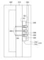
메모리나 CPU(Central Processing Unit) 등의 각종 반도체 디바이스의 검사에, 자동 시험 장치(ATE: Automatic Test Equipment)가 사용된다. ATE는, 시험 대상의 반도체 디바이스(이하, 피시험 디바이스(DUT))에, 시험 신호를 공급하고, 시험 신호에 대한 DUT의 응답을 측정하여, DUT의 양호 여부를 판정하고, 혹은 불량 부분을 특정한다.Automatic test equipment (ATE) is used to test various semiconductor devices such as memory and CPU (Central Processing Unit). ATE supplies a test signal to a semiconductor device under test (hereinafter, device under test (DUT)) and measures the response of the DUT to the test signal to determine whether the DUT is good or bad or to identify a defective part.
도 1은, 종래의 ATE(10)의 블럭도이다. ATE(10)는, 테스터(테스터 본체라고도 한다)(20), 테스트 헤드(30), 인터페이스 장치(40), 핸들러(50)를 구비한다.Fig. 1 is a block diagram of a conventional ATE (10). The ATE (10) is equipped with a tester (also called a tester body) (20), a test head (30), an interface device (40), and a handler (50).
테스터(20)는, ATE(10)를 통괄적으로 제어한다. 구체적으로는, 테스터(20)는, 테스트 프로그램을 실행하고, 테스트 헤드(30)나 핸들러(50)를 제어하여, 측정 결과를 수집한다.The tester (20) comprehensively controls the ATE (10). Specifically, the tester (20) executes a test program and controls the test head (30) or handler (50) to collect measurement results.
테스트 헤드(30)는, DUT(1)에 공급해야 하는 시험 신호를 발생하고, 또한 DUT로부터의 신호(디바이스 신호라 한다)를 검출하는 하드웨어를 구비한다. 구체적으로는, 테스트 헤드(30)는, 핀 일렉트로닉스(PE)(32)나, 전원 회로(미도시) 등을 구비한다. PE(32)는, 드라이버 및 비교기 등을 포함하는 ASIC(Application Specific IC)이다. 종래에 있어서, PE(32)는, PE 보드(34)로 불리는 프린트 기판 상에 실장되고, 테스트 헤드(30)의 내부에 수용되어 있었다.The test head (30) is provided with hardware that generates a test signal to be supplied to the DUT (1) and also detects a signal (called a device signal) from the DUT. Specifically, the test head (30) is provided with pin electronics (PE) (32), a power circuit (not shown), etc. The PE (32) is an ASIC (Application Specific IC) that includes a driver and a comparator, etc. Conventionally, the PE (32) was mounted on a printed circuit board called a PE board (34) and accommodated inside the test head (30).
인터페이스 장치(40)는, 하이픽스라고도 불리고, 테스트 헤드(30)와 DUT(1) 사이의 전기적인 접속을 중계한다. 인터페이스 장치(40)는, 소켓 보드(42)를 구비한다. 소켓 보드(42)에는, 복수의 소켓(44)이 마련되어 있고, 복수의 DUT(1)를 동시 측정 가능하게 되어 있다. 웨이퍼 레벨 시험을 진행하는 ATE의 경우, 소켓 보드(42) 대신에, 프로브 카드가 사용된다.The interface device (40), also called a high-fix, relays the electrical connection between the test head (30) and the DUT (1). The interface device (40) has a socket board (42). The socket board (42) is provided with a plurality of sockets (44), and allows simultaneous measurement of a plurality of DUTs (1). In the case of ATE that performs wafer-level testing, a probe card is used instead of the socket board (42).
복수의 소켓(44)에는, 핸들러(50)에 의해, 복수의 DUT(1)가 로드되어, 소켓(44)에 DUT(1)가 가압된다. 시험 종료 후, 핸들러(50)는, DUT(1)를 언로드하고, 필요에 따라, 양품과 불량품을 분별한다.A plurality of DUTs (1) are loaded into a plurality of sockets (44) by a handler (50), and the DUTs (1) are pressurized into the sockets (44). After the test is completed, the handler (50) unloads the DUTs (1) and, if necessary, distinguishes between good and defective products.
인터페이스 장치(40)는, 소켓 보드(42)와, 테스트 헤드(30)를 접속하는 복수의 케이블(46)을 구비한다. PE(32)가 발생하는 시험 신호는, 케이블(46)을 통해, DUT(1)에 전송되고, DUT(1)가 발생하는 디바이스 신호는, 케이블(46)을 통해 PE(32)에 전송된다.The interface device (40) is equipped with a socket board (42) and a plurality of cables (46) that connect the test head (30). A test signal generated by PE (32) is transmitted to DUT (1) through the cable (46), and a device signal generated by DUT (1) is transmitted to PE (32) through the cable (46).
근래, DRAM(Dynamic Random Access Memory)의 고속화가 진행되고 있다. 그래픽 보드에 탑재되는 GDDR(Graphics Double Data Rate) 메모리에서는, GDDR6X 규격에 있어서, NRZ(Non Return to Zero) 방식에 의해 21Gbps의 전송 속도가 달성되고 있다.Recently, DRAM (Dynamic Random Access Memory) has been accelerating. In the GDDR (Graphics Double Data Rate) memory mounted on graphic boards, a transmission speed of 21 Gbps is achieved through the NRZ (Non Return to Zero) method in the GDDR6X standard.
차세대의 GDDR7에서는, PAM4(Pulse Amplitude Modulation 4)가 채용되어, 전송 속도는 40Gbps까지 향상된다. NRZ 방식도, 해마다 고속화가 진행되고 있어, 차세대에서는, 28Gbps 정도까지 고속화된다.In the next-generation GDDR7, PAM4 (Pulse Amplitude Modulation 4) is adopted, and the transmission speed is improved to 40 Gbps. The NRZ method is also becoming faster every year, and in the next generation, the speed will be increased to around 28 Gbps.
전송 속도가 20Gbps를 넘으면, 종래의 아키텍처를 유용한 메모리 테스터에서의 정확한 측정이 어려워진다. 현상, 28Gbps나 40Gbps의 고속의 메모리를 정확하게 측정할 수 있는 ATE는 시판되고 있지 않다.When the transfer speed exceeds 20 Gbps, it becomes difficult to accurately measure the memory tester using conventional architecture. Currently, there is no commercially available ATE that can accurately measure high-speed memory of 28 Gbps or 40 Gbps.
본 개시는 상기와 같은 상황에서 안출된 것으로서, 그 예시적인 일 목적은, 고속 디바이스를 고정밀도로 시험 가능한 인터페이스 장치, 및 자동 시험 장치의 제공에 있다.The present disclosure has been made under the above circumstances, and one exemplary purpose thereof is to provide an interface device capable of testing a high-speed device with high precision, and an automatic testing device.
본 개시의 일 태양의 인터페이스 장치는, 테스트 헤드와 피시험 디바이스(DUT) 사이에 마련된다. 인터페이스 장치는, DUT가 장착되는 소켓과, 그 제1면에 소켓이 실장되고, 제2면에 복수의 이면 전극을 구비하는 소켓 프린트 기판을 포함하는 소켓 보드와, 그 제1면에, 복수의 변형 전극이 마련되고, 그 제2면에, 복수의 비변형 전극이 마련되어 있고, 복수의 변형 전극이 소켓 프린트 기판의 복수의 이면 전극과 접촉하는 제1 인터포저와, 제1 인터포저의 제2면에 있어서, 복수의 비변형 전극과 접속되는 복수의 전극 패드를 갖는 배선을 구비한다.An interface device of one aspect of the present disclosure is provided between a test head and a device under test (DUT). The interface device includes a socket board including a socket on which a DUT is mounted, a socket printed circuit board having the socket mounted on a first surface thereof and a plurality of back electrodes on a second surface thereof, a first interposer having a plurality of deformable electrodes provided on the first surface thereof and a plurality of non-deformable electrodes provided on the second surface thereof, the plurality of deformable electrodes being in contact with the plurality of back electrodes of the socket printed circuit board, and wiring having a plurality of electrode pads connected to the plurality of non-deformable electrodes on the second surface of the first interposer.
한편, 이상의 구성 요소를 임의로 조합한 것, 구성 요소나 표현을, 방법, 장치 등 사이에서 서로 치환한 것도, 본 발명의 태양으로서 유효하다.Meanwhile, a combination of the above components arbitrarily, or a substitution of components or expressions between methods, devices, etc., is also valid as an aspect of the present invention.
본 개시의 일 태양에 의하면, 고속 디바이스를 양산 시험 가능하게 된다.According to one aspect of the present disclosure, mass production testing of high-speed devices becomes possible.
도 1은, 종래의 ATE의 블럭도이다.
도 2는, 실시형태에 따른 ATE를 나타내는 도면이다.
도 3은, 일 실시예에 따른 인터페이스 장치의 단면도이다.
도 4는, 일 실시예에 따른 프론트 엔드 모듈을 나타내는 도면이다.
도 5는, 도 4의 FEU의 구성예를 나타내는 사시도이다.
도 6은, 도 4의 FEU의 구성예를 나타내는 단면도이다.
도 7은, 핀 일렉트로닉스 IC와 소켓의 접속의 일례를 나타내는 단면도이다.
도 8은, FPC 케이블과 소켓 보드의 접속 부분의 구성예를 나타내는 단면도이다.
도 9는, FPC 케이블과 소켓 보드의 접속 부분의 분해 사시도이다.
도 10의 (a), (b)는, 인터포저의 구조 및 접속을 설명하는 단면도이다.
도 11은, FPC 케이블과 핀 일렉트로닉스 PCB의 접속 부분의 구성예를 나타내는 단면도이다.
도 12는, FPC 케이블과 핀 일렉트로닉스 PCB의 접속 부분의 분해 사시도이다.Figure 1 is a block diagram of a conventional ATE.
Fig. 2 is a drawing showing an ATE according to an embodiment.
FIG. 3 is a cross-sectional view of an interface device according to one embodiment.
FIG. 4 is a diagram illustrating a front-end module according to one embodiment.
Figure 5 is a perspective view showing an example of the configuration of the FEU of Figure 4.
Fig. 6 is a cross-sectional view showing an example of the configuration of the FEU of Fig. 4.
Fig. 7 is a cross-sectional view showing an example of the connection between a pin electronics IC and a socket.
Figure 8 is a cross-sectional view showing an example of the configuration of a connection portion between an FPC cable and a socket board.
Figure 9 is an exploded perspective view of the connection portion of the FPC cable and socket board.
Figures 10 (a) and (b) are cross-sectional views explaining the structure and connection of the interposer.
Fig. 11 is a cross-sectional view showing an example of the configuration of a connection portion between an FPC cable and a pin electronics PCB.
Figure 12 is an exploded perspective view of the connection portion of the FPC cable and the pin electronics PCB.
(실시형태의 개요)(Overview of the implementation)
본 개시의 몇몇 예시적인 실시형태의 개요를 설명한다. 이 개요는, 후술하는 상세한 설명의 서론으로서, 실시형태의 기본적인 이해를 목적으로 하여, 1개 또는 복수의 실시형태의 몇몇 개념을 간략화하여 설명하는 것이고, 발명 혹은 개시의 범위를 한정하는 것이 아니다. 이 개요는, 생각되는 모든 실시형태의 포괄적인 개요가 아니고, 모든 실시형태의 중요한 요소를 특정하는 것도, 일부 또는 모든 태양의 범위를 선긋기하는 것도 의도하고 있지 않다. 편의상, “일 실시형태”는, 본 명세서에 개시하는 하나의 실시형태(실시예나 변형예) 또는 복수의 실시형태(실시예나 변형예)를 가리키는 것으로 사용하는 경우가 있다.Hereinafter, an overview of some exemplary embodiments of the present disclosure will be described. This overview is intended as a prelude to the detailed description that follows, and is intended to provide a basic understanding of the embodiments by briefly describing some concepts of one or more embodiments, and is not intended to limit the scope of the invention or disclosure. This overview is not intended to be a comprehensive overview of all contemplated embodiments, nor is it intended to identify key elements of all embodiments, nor to delineate the scope of any or all aspects. For convenience, the term “one embodiment” may sometimes be used to refer to one embodiment (an embodiment or a variation) or multiple embodiments (an embodiment or a variation) disclosed herein.
초고속의 메모리 디바이스를 시험 가능한 ATE를 실현하기 위해서는, 신호원(드라이버)과 DUT 사이의 전송 거리를 최단화할 필요가 있다. 종래에는 동축 케이블을 사용한 마더보드(MB)에 의해, 핀 일렉트로닉스 보드(PE)와 DUT 사이의 전송을 담당하고 있었지만, 동축 케이블의 전송 손실 및 동축 케이블과 기판과의 접속에 필요한 커넥터의 전송 손실, 나아가 기판 상의 핀 일렉트로닉스 IC에서 커넥터까지의 배선 인출과 같은 전송 매체의 접속점이나, 접속 부분에서의 모드 변환에 따른 신호 반사 등의 신호 열화 요인이 많아, 고속 신호를 정확하게 전송하기에는 불리했다. 본 개시는, 이와 같은 식견을 바탕으로 이루어진 것이다. 본 개시에서는, 전송로에 있어서의 손실을 저감하는 것에 의해, 고속 신호의 전송을 가능하게 하는 방식을 제안한다.In order to realize an ATE capable of testing ultra-high-speed memory devices, it is necessary to minimize the transmission distance between a signal source (driver) and a DUT. Conventionally, transmission between a pin electronics board (PE) and a DUT has been handled by a motherboard (MB) using a coaxial cable, but there are many signal deterioration factors such as transmission loss of the coaxial cable, transmission loss of the connector required for connection between the coaxial cable and the board, and signal reflection due to mode conversion at the connection point of the transmission medium such as wiring lead-out from the pin electronics IC to the connector on the board, and the like, making it disadvantageous for accurately transmitting high-speed signals. The present disclosure has been made based on such insight. The present disclosure proposes a method for enabling transmission of high-speed signals by reducing loss in a transmission path.
일 실시형태에 따른 인터페이스 장치는, 테스트 헤드와 피시험 디바이스(DUT) 사이에 마련된다. 인터페이스 장치는, DUT가 장착되는 소켓과, 그 제1면에 소켓이 실장되고, 제2면에 복수의 이면 전극을 구비하는 소켓 프린트 기판을 포함하는 소켓 보드와, 그 제1면에, 복수의 변형 전극이 마련되고, 그 제2면에, 복수의 비변형 전극이 마련되어 있고, 복수의 변형 전극이 소켓 프린트 기판의 복수의 이면 전극과 접촉하는 제1 인터포저와, 제1 인터포저의 제2면에 있어서, 복수의 비변형 전극과 접속되는 복수의 전극 패드를 갖는 배선을 구비한다.An interface device according to one embodiment is provided between a test head and a device under test (DUT). The interface device comprises a socket board including a socket on which a DUT is mounted, a socket printed circuit board having the socket mounted on a first surface thereof and a plurality of back electrodes on a second surface thereof, a first interposer having a plurality of deformable electrodes provided on the first surface thereof and a plurality of non-deformable electrodes provided on the second surface thereof, the plurality of deformable electrodes being in contact with the plurality of back electrodes of the socket printed circuit board, and wiring having a plurality of electrode pads connected to the plurality of non-deformable electrodes on the second surface of the first interposer.
종래의 아키텍처에서는, 케이블을 탈착 가능하게 하고자 하는 경우, LIF(Low Insertion Force) 커넥터나 ZIF(Zero Insertion Force) 커넥터가 채용되고 있었지만, 이들의 커넥터는, 고주파 영역에서 무시할 수 없는 손실을 갖고 있다. 본 실시형태에서는, LIF 커넥터나 ZIF 커넥터 대신에, 고주파 특성이 뛰어난 인터포저를 이용하여 전기적 컨택트를 취하기 때문에, 커넥터의 손실을 저감할 수 있다. 이에 의해 파형 왜곡을 개선하여, 고속의 디바이스를 시험하는 것이 가능해진다.In conventional architectures, when it is desired to make a cable detachable, a LIF (Low Insertion Force) connector or a ZIF (Zero Insertion Force) connector is employed, but these connectors have non-negligible losses in the high-frequency range. In the present embodiment, instead of a LIF connector or a ZIF connector, an interposer with excellent high-frequency characteristics is used to make electrical contact, so that connector loss can be reduced. This improves waveform distortion, making it possible to test high-speed devices.
일 실시형태에 있어서, 배선은, FPC 케이블이어도 좋다. 배선으로서 동축 케이블을 이용하는 경우, 동축 케이블과 인터포저 사이에, 기판을 추가할 필요가 있어, 손실이 증가하는 요인이 될 수 있다. 이에 대해, 배선으로서 FPC 케이블을 상용하는 것에 의해, FPC 케이블과 인터포저를 직접 접촉시킬 수 있어, 손실을 저감할 수 있다.In one embodiment, the wiring may be an FPC cable. When a coaxial cable is used as the wiring, it is necessary to add a substrate between the coaxial cable and the interposer, which may be a factor in increasing loss. In contrast, by using an FPC cable as the wiring, the FPC cable and the interposer can be brought into direct contact, thereby reducing the loss.
일 실시형태에 있어서, 인터페이스 장치는, 복수의 핀 일렉트로닉스 IC(Integrated Circuit)가 모듈화되어 구성되는 프론트 엔드 모듈을 구비해도 좋다. 프론트 엔드 모듈과, 소켓 프린트 기판 사이가 배선을 통해 접속되어도 좋다. 핀 일렉트로닉스 IC를 구비하는 프론트 엔드 모듈을, 인터페이스 장치에 내장하는 것에 의해, 핀 일렉트로닉스 IC를, DUT의 지근에 배치하는 것이 가능해지고, 시험 신호 및 디바이스 신호의 전송 거리를 종래에 비해 대폭으로 짧게 할 수 있다. 이에 의해 고주파 성분의 손실을 억제할 수 있어, 고속의 시험 신호 및 디바이스 신호를 전송하는 것이 가능해지고, 나아가서는 정확한 시험이 가능해진다.In one embodiment, the interface device may have a front-end module in which a plurality of pin electronics ICs (Integrated Circuits) are modularized and configured. The front-end module and the socket printed circuit board may be connected via wiring. By incorporating a front-end module having a pin electronics IC into the interface device, it becomes possible to place the pin electronics IC in close proximity to the DUT, and the transmission distance of test signals and device signals can be significantly shortened compared to the conventional one. As a result, loss of high-frequency components can be suppressed, high-speed test signals and device signals can be transmitted, and further, accurate testing becomes possible.
일 실시형태에 있어서, 프론트 엔드 모듈은, 그 표면에 핀 일렉트로닉스 IC가 실장되는 핀 일렉트로닉스 프린트 기판을 더 포함해도 좋다. 인터페이스 장치는, 그 제1면에, 복수의 변형 전극이 마련되고, 그 제2면에, 복수의 비변형 전극이 마련되어 있고, 복수의 변형 전극이 핀 일렉트로닉스 프린트 기판의 이면 전극과 접촉하고, 복수의 비변형 전극이 배선에 마련된 복수의 전극 패드와 접속되는 제2 인터포저를 더 구비해도 좋다. 핀 일렉트로닉스 회로와 배선 사이의 접속 부분에도, 인터포저를 채용하는 것에 의해, 더 손실을 저감할 수 있다.In one embodiment, the front-end module may further include a pin electronics printed circuit board having a pin electronics IC mounted on a surface thereof. The interface device may further include a second interposer having a plurality of deformable electrodes provided on a first surface thereof, a plurality of non-deformable electrodes provided on a second surface thereof, the plurality of deformable electrodes being in contact with the back electrodes of the pin electronics printed circuit board, and the plurality of non-deformable electrodes being connected to a plurality of electrode pads provided on the wiring. By employing the interposer also at a connection portion between the pin electronics circuit and the wiring, loss can be further reduced.
일 실시형태에 있어서, 인터페이스 장치는, 소켓 보드 대신에 프로브 카드를 구비하는 웨이퍼 마더보드여도 좋다. 제1 인터포저는, 프로브 카드와 상기 배선을 접속해도 좋다.In one embodiment, the interface device may be a wafer motherboard having a probe card instead of a socket board. The first interposer may connect the probe card and the above wiring.
일 실시형태에 따른 자동 시험 장치는, 테스터 본체와, 테스트 헤드와, 테스트 헤드에 접속되는 인터페이스 장치를 구비해도 좋다.An automatic test device according to one embodiment may include a tester body, a test head, and an interface device connected to the test head.
(실시형태)(Implementation form)
이하, 바람직한 실시형태에 대해, 도면을 참조하면서 설명한다. 각 도면에 도시되는 동일 또는 동등의 구성 요소, 부재, 처리에는, 동일한 부호를 부여하고, 적절히 중복된 설명은 생략한다. 또한, 실시형태는, 개시 및 발명을 한정하는 것이 아닌 예시이고, 실시형태에 기술되는 모든 특징이나 그 조합은, 반드시 개시 및 발명의 본질적인 것이라고는 할 수 없다.Hereinafter, preferred embodiments will be described with reference to the drawings. The same or equivalent components, members, and processes illustrated in each drawing are given the same reference numerals, and any duplicate descriptions are omitted as appropriate. In addition, the embodiments are examples that do not limit the disclosure and invention, and all features or combinations thereof described in the embodiments are not necessarily essential to the disclosure and invention.
또한 도면에 기재되는 각 부재의 치수(두께, 길이, 폭 등)는, 이해의 용이하게 하기 위해 적절히, 확대 축소되어 있는 경우가 있다. 나아가 복수의 부재의 치수는, 반드시 그들의 대소 관계를 나타내고 있다고는 할 수 없고, 도면상에서, 어떤 부재 A가, 다른 부재 B보다 두껍게 도시되어 있어도, 부재 A가 부재 B보다 얇은 경우도 있을 수 있다.In addition, the dimensions (thickness, length, width, etc.) of each member described in the drawing may be appropriately enlarged or reduced for ease of understanding. Furthermore, the dimensions of multiple members do not necessarily represent their size relationship, and even if a member A is depicted as thicker than another member B in the drawing, there may be cases where member A is thinner than member B.
본 명세서에 있어서, “부재 A가 부재 B와 접속된 상태”란, 부재 A와 부재 B가 물리적으로 직접적으로 접속되는 경우 이외에, 부재 A와 부재 B가, 그들의 전기적인 접속 상태에 실질적인 영향을 미치지 않는, 혹은 그들의 결합에 의해 발휘되는 기능이나 효과를 손상시키지 않는, 기타의 부재를 통해 간접적으로 접속되는 경우도 포함한다.In this specification, the term “a state in which member A is connected to member B” includes, in addition to cases in which members A and B are physically directly connected, cases in which members A and B are indirectly connected through other members that do not substantially affect their electrical connection state or do not impair the function or effect exerted by their combination.
마찬가지로, “부재 C가, 부재 A와 부재 B 사이에 접속된(마련된) 상태”란, 부재 A와 부재 C, 혹은 부재 B와 부재 C가 직접적으로 접속되는 경우 이외에, 그들의 전기적인 접속 상태에 실질적인 영향을 미치지 않는, 혹은 그들의 결합에 의해 발휘되는 기능이나 효과를 손상시키지 않는, 기타의 부재를 통해 간접적으로 접속되는 경우도 포함한다.Likewise, the “state in which absence C is connected (provided) between absence A and absence B” includes, in addition to cases in which absence A and absence C, or absence B and absence C, are directly connected, cases in which they are indirectly connected through other absences that do not substantially affect their electrical connection state or do not impair the function or effect exerted by their combination.
도 2는, 실시형태에 따른 ATE(100)를 나타내는 도면이다. ATE(100)는, 테스터(120), 테스트 헤드(130), 핸들러(150) 및 인터페이스 장치(200)를 구비한다.Fig. 2 is a drawing showing an ATE (100) according to an embodiment. The ATE (100) has a tester (120), a test head (130), a handler (150), and an interface device (200).
테스터(120)는, ATE(100)를 통괄적으로 제어한다. 구체적으로는, 테스터(120)는, 테스트 프로그램을 실행하고, 테스트 헤드(130)나 핸들러(150)를 제어하여, 측정 결과를 수집한다.The tester (120) comprehensively controls the ATE (100). Specifically, the tester (120) executes a test program and controls the test head (130) or handler (150) to collect measurement results.
핸들러(150)는, DUT(1)를, 인터페이스 장치(200)에 공급(로드)하고, 시험 완료된 DUT(1)를, 인터페이스 장치(200)부터 언로드한다. 또한 핸들러(150)는, DUT(1)를, 양품과 불량품에 분별한다.The handler (150) supplies (loads) the DUT (1) to the interface device (200) and unloads the tested DUT (1) from the interface device (200). In addition, the handler (150) distinguishes the DUT (1) into good and defective products.
인터페이스 장치(200)는, 소켓 보드(210), 배선(220) 및 프론트 엔드 모듈(300)을 구비한다.The interface device (200) has a socket board (210), wiring (220), and a front end module (300).
본 실시형태에 있어서, 복수의 핀 일렉트로닉스 IC(PE-IC)(400)는, 테스트 헤드(130) 내가 아닌, 인터페이스 장치(200)에 마련되어 있다. 핀 일렉트로닉스 IC(400)는, 시험 신호를 발생하는 드라이버나, 디바이스 신호를 수신하는 비교기가 집적화되는 특정 용도용 집적 회로(ASIC: Application Specific IC)이다. 시험 신호 및 디바이스 신호는, NRZ 신호 혹은 PAM4 신호이다.In the present embodiment, a plurality of pin electronics ICs (PE-ICs) (400) are provided in an interface device (200), not in a test head (130). The pin electronics IC (400) is an application specific integrated circuit (ASIC) in which a driver for generating a test signal and a comparator for receiving a device signal are integrated. The test signal and the device signal are NRZ signals or PAM4 signals.
더욱 구체적으로는, 복수의 핀 일렉트로닉스 IC(400)는 모듈화되어 있다. 이 모듈을 프론트 엔드 모듈(300)이라 부른다.More specifically, a plurality of pin electronics ICs (400) are modularized. This module is called a front-end module (300).
소켓 보드(210)에는, 복수의 소켓(212)이 마련되어 있다. 소켓(212)에는, DUT(1)가 장착된다. 프론트 엔드 모듈(300)과 소켓(212) 사이는, 배선(220)을 통해 접속된다.A plurality of sockets (212) are provided on the socket board (210). A DUT (1) is mounted on the socket (212). The front end module (300) and the socket (212) are connected through wiring (220).
이상이 ATE(100)의 구성이다.The above is the configuration of ATE (100).
이 ATE(100)에 의하면, 복수의 핀 일렉트로닉스 IC(400)를 모듈화하여 구성되는 프론트 엔드 모듈(300)을, 인터페이스 장치(200)에 내장하는 것에 의해, 핀 일렉트로닉스 IC(400)를, DUT(1)의 지근에 배치하는 것이 가능해진다. 이에 의해, 시험 신호 및 디바이스 신호의 전송 거리를, 종래에 비해 대폭으로 짧게 할 수 있다.According to this ATE (100), by incorporating a front-end module (300) configured by modularizing a plurality of pin electronics ICs (400) into an interface device (200), it becomes possible to place the pin electronics IC (400) in close proximity to the DUT (1). As a result, the transmission distance of test signals and device signals can be significantly shortened compared to conventional methods.
예를 들면, 종래의 ATE에 있어서, 핀 일렉트로닉스 IC와 소켓 보드 사이는, 길이 500mm~600mm 정도의 동축 케이블로 접속되어 있었지만, 본 실시형태에서는, 배선(220)의 길이를, 100mm~150mm 정도까지 짧게 할 수 있다. 이에 의해 고주파 성분의 손실을 대폭 저감할 수 있어, 고속의 시험 신호 및 디바이스 신호를 전송하는 것이 가능해진다. 이 인터페이스 장치(200)를 구비하는 ATE(100)는, 20Gbps를 넘는 고속 메모리의 시험이 가능해진다.For example, in conventional ATE, the pin electronics IC and the socket board were connected by a coaxial cable having a length of about 500 mm to 600 mm, but in this embodiment, the length of the wiring (220) can be shortened to about 100 mm to 150 mm. This significantly reduces the loss of high-frequency components, making it possible to transmit high-speed test signals and device signals. An ATE (100) equipped with this interface device (200) can test high-speed memories exceeding 20 Gbps.
본 개시는, 도 2의 블록도나 회로도로서 파악되는, 혹은 상술한 설명으로부터 도출되는 다양한 장치, 방법에 이르는 것이고, 특정의 구성에 한정되는 것은 아니다. 이하, 본 개시의 범위를 좁히기 위한 것은 아니고, 본 개시나 발명의 본질이나 동작의 이해를 돕고, 또한 그들을 명확화하기 위해, 더욱 구체적인 구성예나 실시예를 설명한다.The present disclosure covers various devices and methods that are understood as block diagrams or circuit diagrams of FIG. 2, or derived from the above-described description, and is not limited to a specific configuration. Hereinafter, more specific configuration examples or embodiments will be described, not to narrow the scope of the present disclosure, but to help understand the nature or operation of the present disclosure or invention, and also to clarify them.
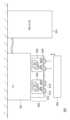
도 3은, 일 실시예에 따른 인터페이스 장치(200A)의 단면도이다. 도 3에는, 1개의 DUT에 관련되는 구성만이 도시된다. 이 실시예에 있어서, 인터페이스 장치(200A)는, 마더보드(230)와, 마더보드(230)에 대해 탈착 가능한 소켓 보드(210)를 구비한다. 소켓 보드(210)는, 소켓(212), 소켓 프린트 기판(소켓 PCB)(214), 소켓 보드측 커넥터(216)를 구비한다.FIG. 3 is a cross-sectional view of an interface device (200A) according to one embodiment. In FIG. 3, only a configuration related to one DUT is illustrated. In this embodiment, the interface device (200A) has a motherboard (230) and a socket board (210) that is detachable from the motherboard (230). The socket board (210) has a socket (212), a socket printed circuit board (socket PCB) (214), and a socket board-side connector (216).
프론트 엔드 모듈(300A)은, 복수의 핀 일렉트로닉스 IC(400)가 실장되는 복수의 프린트 기판(핀 일렉트로닉스 PCB)(310)을 구비한다. 복수의 핀 일렉트로닉스 PCB(310)는, DUT의 면(표면 및 이면), 즉 소켓 보드(210)의 면(S1)에 대해 수직인 방향으로 배치된다. 본 실시형태에서는, 소켓 보드(210)는, 지면과 수평이고, 따라서 복수의 핀 일렉트로닉스 PCB(310)는, 중력 방향과 평행해지도록 배치된다.The front-end module (300A) has a plurality of printed circuit boards (pin electronics PCBs) (310) on which a plurality of pin electronics ICs (400) are mounted. The plurality of pin electronics PCBs (310) are arranged in a direction perpendicular to a surface (front and back) of the DUT, that is, a surface (S1) of the socket board (210). In the present embodiment, the socket board (210) is horizontal to the ground, and therefore, the plurality of pin electronics PCBs (310) are arranged so as to be parallel to the direction of gravity.
프론트 엔드 모듈(300A)은, 플레이트 형상의 냉각 장치(이하, 콜드 플레이트라 한다)(320)를 더 구비한다. 콜드 플레이트(320)는, 냉매가 유통하는 유로를 구비한다.The front end module (300A) further includes a plate-shaped cooling device (hereinafter referred to as a cold plate) (320). The cold plate (320) includes a path through which refrigerant circulates.
복수의 핀 일렉트로닉스 PCB(310a, 310b) 및 콜드 플레이트(320)는, 핀 일렉트로닉스 IC(400)가 콜드 플레이트(320)와 열적으로 결합하는 형태로 적층되어 있다.A plurality of pin electronics PCBs (310a, 310b) and a cold plate (320) are laminated in a form in which a pin electronics IC (400) is thermally coupled to the cold plate (320).
마더보드(230)는, 소켓 보드측 커넥터(232), 스페이싱 프레임(234), 중계 커넥터(236)를 구비한다. 프론트 엔드 모듈(300A)은, 스페이싱 프레임(234)에 대해 고정되어 있다. 중계 커넥터(236)는, 테스트 헤드측 커넥터(132)와 전기적 및 기계적으로 결합한다.The motherboard (230) has a socket board side connector (232), a spacing frame (234), and a relay connector (236). The front end module (300A) is fixed to the spacing frame (234). The relay connector (236) is electrically and mechanically coupled to the test head side connector (132).
상세한 것은 후술하는 바와 같이, 배선(220)은, 종래의 동축 케이블 대신에, 플렉시블 기판(FPC: Flexible printed circuits)으로 구성되는 케이블(FPC 케이블이라고도 한다)을 사용할 수 있다.As described in detail later, instead of a conventional coaxial cable, the wiring (220) may use a cable composed of a flexible printed circuit (FPC: Flexible printed circuits) (also called an FPC cable).
한편, 핀 일렉트로닉스 PCB(310)와 중계 커넥터(236) 사이의 배선(224)에는, 핀 일렉트로닉스 IC(400)에 대한 제어 신호만 전송하고, 시험 신호나 디바이스 신호는 전송하지 않는다. 그 때문에 배선(224)은, 동축 케이블을 이용해도 좋다.Meanwhile, only the control signal for the pin electronics IC (400) is transmitted through the wiring (224) between the pin electronics PCB (310) and the relay connector (236), and no test signal or device signal is transmitted. Therefore, the wiring (224) may use a coaxial cable.
복수의 핀 일렉트로닉스 IC(400)는, 핀 일렉트로닉스 PCB(310) 상에서, 핀 일렉트로닉스 PCB(310)의 상하 방향의 중앙보다도, DUT에 치우쳐(소켓 보드(210)에 치우쳐) 실장된다. 이에 의해, 핀 일렉트로닉스 PCB(310) 상에서의, 시험 신호 및 디바이스 신호의 전송 거리를 짧게 할 수 있어, 고속의 신호 전송이 가능해진다.A plurality of pin electronics ICs (400) are mounted on a pin electronics PCB (310) with a distance from the center of the vertical direction of the pin electronics PCB (310) toward the DUT (with a distance from the socket board (210)). As a result, the transmission distance of test signals and device signals on the pin electronics PCB (310) can be shortened, thereby enabling high-speed signal transmission.
예를 들면, 복수의 핀 일렉트로닉스 IC(400)는, 핀 일렉트로닉스 PCB(310)의 DUT측의 1변으로부터, 50mm 이내에 배치하는 것이 바람직하고, 30mm 이내에 배치할 수 있으면, 더욱 전송 거리를 짧게 할 수 있다.For example, it is preferable that a plurality of pin electronics ICs (400) be placed within 50 mm from one side of the DUT side of the pin electronics PCB (310), and if they can be placed within 30 mm, the transmission distance can be further shortened.
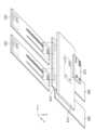
도 4는, 일 실시예에 따른 프론트 엔드 모듈(300B)을 나타내는 도면이다.FIG. 4 is a drawing showing a front end module (300B) according to one embodiment.
1개의 DUT(1)에는, 2×M개(M≥1)의 핀 일렉트로닉스 IC(400)가 할당되어 있다. 복수의 DUT 및 핀 일렉트로닉스 IC(400)에는, A~D의 첨자를 붙여, 필요에 따라 구별한다. 이 예에서는, DUT(1)가, 192I/O를 갖고, 핀 일렉트로닉스 IC(400)가 24I/O를 갖는 경우, 1개의 DUT당, 192/24=8개(즉 M=4)의 핀 일렉트로닉스 IC(400)가 할당된다.To one DUT (1), 2×M (M≥1) pin electronics ICs (400) are allocated. Multiple DUTs and pin electronics ICs (400) are assigned subscripts A to D to distinguish them as needed. In this example, when DUT (1) has 192 I/O and the pin electronics IC (400) has 24 I/O, 192/24=8 (i.e., M=4) pin electronics ICs (400) are allocated per DUT.
프론트 엔드 모듈(300B)은, 복수 N개(N≥2)의 DUT(1)마다 분할하여 구성되고, 이 분할 단위를 프론트 엔드 유닛(FEU)이라 부른다. 이 예에서는 4개의 DUT에 대응하는 블록이, 1개의 FEU를 구성하고 있고, 1개의 FEU는, 2×M×N개=2×4×4=32개의 핀 일렉트로닉스 IC(400)를 구비한다.The front-end module (300B) is configured by dividing each of a plurality of N (N≥2) DUTs (1), and this division unit is called a front-end unit (FEU). In this example, blocks corresponding to four DUTs constitute one FEU, and one FEU has 2×M×N=2×4×4=32 pin electronics ICs (400).
도 4에는, 2개의 FEU가 도시되지만, 실제로는 프론트 엔드 모듈(300B)은, 2개 이상의 FEU를 구비할 수 있다. 예를 들면 64개의 동시 측정 가능한 ATE에서는, 64/4=16개의 FEU가 마련되고, 프론트 엔드 모듈(300B) 전체로서는, 64×192I/O=12288I/O를 구비하게 된다.In Fig. 4, two FEUs are illustrated, but in reality, the front-end module (300B) may be equipped with two or more FEUs. For example, in an ATE capable of 64 simultaneous measurements, 64/4=16 FEUs are provided, and the entire front-end module (300B) is equipped with 64×192I/O=12288I/O.
도 5는, 도 4의 FEU의 구성예를 나타내는 사시도이다. 4개의 DUT에 대응하는 소켓(212A~212D)은, 2행 2열의 매트릭스 모양으로 배치된다. 1개의 DUT(1A)에 착목하면, 그에 할당되는 8개의 핀 일렉트로닉스 IC(400A)는, X 방향으로 배열되는 4장의 핀 일렉트로닉스 PCB(310a~310d)에 2개씩으로 나누어 실장된다. 소켓(212)이 실장되는 소켓 PCB(214)는, DUT마다 분할되어 있어도 좋고, 4개의 DUT에 대응하는 소켓 PCB(214)가, 1장의 기판으로서 일체로 구성되어도 좋다.Fig. 5 is a perspective view showing an example of the configuration of the FEU of Fig. 4. Sockets (212A to 212D) corresponding to four DUTs are arranged in a matrix shape of two rows and two columns. When focusing on one DUT (1A), eight pin electronics ICs (400A) assigned to it are divided into two each and mounted on four pin electronics PCBs (310a to 310d) arranged in the X direction. The socket PCB (214) on which the socket (212) is mounted may be divided for each DUT, or the socket PCBs (214) corresponding to four DUTs may be configured integrally as a single substrate.
1장의 핀 일렉트로닉스 PCB(310)에 실장되는 2개의 핀 일렉트로닉스 IC(400A)는, Y방향으로 배열되어 배치된다. 2개의 핀 일렉트로닉스 IC(400A)는, DUT(1A)로부터 등거리의 위치에 배치되어 있다.Two pin electronics ICs (400A) mounted on a single pin electronics PCB (310) are arranged in the Y direction. The two pin electronics ICs (400A) are arranged at an equidistant position from the DUT (1A).
도 6은, 도 4의 FEU의 구성예를 나타내는 단면도이다. 도 3에 나타낸 바와 같이, 2장의 핀 일렉트로닉스 PCB(310a)와 PCB(310b) 사이에는, 콜드 플레이트(320)가 마련된다. 마찬가지로, 2장의 핀 일렉트로닉스 PCB(310c, 310d) 사이에도, 콜드 플레이트(320)가 마련된다. 상술한 바와 같이, 핀 일렉트로닉스 IC(400)는, 핀 일렉트로닉스 PCB(310) 상의 소켓 보드(210)에 가까운 곳에 실장되어 있다. 냉각 효율을 높이기 위해, 핀 일렉트로닉스 IC(400)는 베어 칩으로 할 수 있고, 핀 일렉트로닉스 IC(400)와 콜드 플레이트(320)는, thermal interface material(TIM)(322)을 통해 열적으로 결합하고 있다.FIG. 6 is a cross-sectional view showing an example of the configuration of the FEU of FIG. 4. As shown in FIG. 3, a cold plate (320) is provided between two pin electronics PCBs (310a) and PCB (310b). Similarly, a cold plate (320) is also provided between two pin electronics PCBs (310c, 310d). As described above, the pin electronics IC (400) is mounted close to the socket board (210) on the pin electronics PCB (310). In order to increase cooling efficiency, the pin electronics IC (400) can be a bare chip, and the pin electronics IC (400) and the cold plate (320) are thermally coupled via a thermal interface material (TIM) (322).
또한 FEU를, Y 축을 따라 평면시했을 때, X 방향으로 적층되는 4장(M장)의 핀 일렉트로닉스 PCB(310a~310d)의 중심 위치에, DUT의 중심, 즉 소켓(212A)이 위치하고 있다.In addition, when the FEU is planarized along the Y-axis, the center of the DUT, i.e., the socket (212A), is located at the center of four (M) pin electronics PCBs (310a to 310d) stacked in the X direction.
이상이 FEU의 구성이다.This is the composition of FEU.
이 FEU의 이점을 설명한다. 첨자 A를 붙인 DUT(1A)에 착목한다. 1개의 DUT(1A)에 대응하는 복수(이 예에서는 8개)의 핀 일렉트로닉스 IC(400A)를, 4장의 핀 일렉트로닉스 PCB(310a~310d)에 2개씩 실장하는 것에 의해, 8개의 핀 일렉트로닉스 IC(400A) 각각으로부터, 소켓(212A)까지의 거리를 균일화할 수 있다. 이에 의해 각 핀 일렉트로닉스 IC(400A)에서 소켓(212A)(DUT(1A))까지의 전송 선로의 손실을 균일화할 수 있고, 정확한 시험이 가능해진다.Hereinafter, the advantages of this FEU will be explained. Focus on a DUT (1A) with a suffix A. By mounting two (in this example, eight) pin electronics ICs (400A) corresponding to one DUT (1A) on four pin electronics PCBs (310a to 310d), the distance from each of the eight pin electronics ICs (400A) to the socket (212A) can be uniformized. This uniformizes the loss of the transmission line from each pin electronics IC (400A) to the socket (212A) (DUT (1A)), and enables accurate testing.
이어서, 핀 일렉트로닉스 IC(400)와 소켓(212)의 전기적인 접속에 대해 설명한다.Next, the electrical connection between the pin electronics IC (400) and the socket (212) is described.
도 7은, 핀 일렉트로닉스 IC와 소켓(DUT(1))의 접속의 일례를 나타내는 단면도이다. 시험 신호 및 디바이스 신호가 전송하는 전송로, 즉 핀 일렉트로닉스 PCB(310)와 소켓 보드(210) 사이의 배선(220)은, FPC 케이블(222)이 사용된다.Fig. 7 is a cross-sectional view showing an example of a connection between a pin electronics IC and a socket (DUT (1)). A FPC cable (222) is used as a transmission path for transmitting test signals and device signals, that is, wiring (220) between a pin electronics PCB (310) and a socket board (210).
핀 일렉트로닉스 PCB(310)와 소켓 보드(210) 사이의 배선(220)으로서, 동축 케이블을 사용하면, 동축 케이블의 강성에 기인하여, 핀 일렉트로닉스 PCB(310)와 소켓 보드(210)의 최단 거리가 제약된다. 또한 이에 대해, FPC 케이블(222)을 상용하는 것에 의해, 그 유연성에 의해 핀 일렉트로닉스 PCB(310)와 소켓 보드(210)의 거리(h)를, 동축 케이블을 사용한 경우에 비해 단축할 수 있고, 시험 신호 및 디바이스 신호의 전송 거리를 짧게 할 수 있다.When a coaxial cable is used as the wiring (220) between the pin electronics PCB (310) and the socket board (210), the shortest distance between the pin electronics PCB (310) and the socket board (210) is limited due to the rigidity of the coaxial cable. In addition, by commercially using an FPC cable (222), the distance (h) between the pin electronics PCB (310) and the socket board (210) can be shortened compared to the case where a coaxial cable is used due to its flexibility, and the transmission distance of a test signal and a device signal can be shortened.
종래의 시험 장치에서는, 소켓 보드(210)를 탈착 가능하게 하고자 하는 경우, LIF(Low Inserstion Force) 커넥터를 사용하는 것이 일반적이었다. 이 LIF 커넥터는, 14GHz보다 높은 주파수 대역에 있어서, -3dB 정도의 무시할 수 없는 손실을 갖고 있어, 28Gbps 혹은 40Gbps의 고속 전송에 있어서는, 파형 왜곡의 원인이 된다. 배선(220)에 FPC 케이블(222)을 상용하는 것에 의해, LIF 커넥터가 불필요해지기 때문에, 손실(고주파 대역의 감쇠)에 기인하는 파형 왜곡을 억제할 수 있어, 정확한 시험이 가능해진다.In conventional test equipment, when it is desired to make the socket board (210) detachable, it is common to use a LIF (Low Inserstion Force) connector. This LIF connector has a non-negligible loss of about -3 dB in a frequency band higher than 14 GHz, and thus causes waveform distortion in high-speed transmission of 28 Gbps or 40 Gbps. By using an FPC cable (222) for wiring (220), the LIF connector becomes unnecessary, and thus waveform distortion caused by loss (attenuation of high-frequency band) can be suppressed, enabling accurate testing.
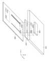
도 8은, FPC 케이블(222)과 소켓 보드(210)의 접속 부분의 구성예를 나타내는 단면도이다. 도 9는, FPC 케이블(222)과 소켓 보드(210)의 접속 부분의 분해 사시도이다.Fig. 8 is a cross-sectional view showing an example of the configuration of a connection portion between an FPC cable (222) and a socket board (210). Fig. 9 is an exploded perspective view of the connection portion between an FPC cable (222) and a socket board (210).
소켓 보드(210)는, 소켓(212) 및 소켓 PCB(214)를 포함한다. 소켓 PCB(214)는, 배선층과 절연층을 포함하는 다층 기판이다. 배선층에는, 신호 경로를 수평 방향으로 이동시키는 배선이 형성되고, 절연층에는, 신호 경로를 수직 방향으로 이동시키는 비아 홀(VH)이 형성되어 있다. 시험 신호 및 디바이스 신호가 전송하는 경로는, 가능한 한 수평 방향(X 방향 및 Y방향)으로 이동하지 않고, 소켓 보드(210)의 이면까지 인출되는 것이 바람직하다. 반대로, 전원 신호나 주파수가 낮은 제어 신호에 관해서는, 소켓 PCB(214)의 내부에서, 수평 방향으로 깔아도 좋다.The socket board (210) includes a socket (212) and a socket PCB (214). The socket PCB (214) is a multilayer substrate including a wiring layer and an insulating layer. In the wiring layer, a wiring is formed to move a signal path in a horizontal direction, and in the insulating layer, a via hole (VH) is formed to move a signal path in a vertical direction. It is preferable that the path through which a test signal and a device signal are transmitted is extended to the back surface of the socket board (210) without moving in a horizontal direction (X direction and Y direction) as much as possible. Conversely, power signals or low-frequency control signals may be laid in a horizontal direction inside the socket PCB (214).
FPC 케이블(222)과 소켓 보드(210)는, 소켓 보드측 커넥터(216)에 의해 접속된다. 소켓 보드측 커넥터(216)는, 인터포저(218)와, 케이블 클램프(219)를 포함한다.The FPC cable (222) and the socket board (210) are connected by a socket board-side connector (216). The socket board-side connector (216) includes an interposer (218) and a cable clamp (219).
인터포저(218)의 표면에 노출되는 전극은, 소켓 PCB(214)의 이면에 노출되는 전극과 전기적으로 접속되어 있다. FPC 케이블(222)은, 인터포저(218)의 이면 전극과 접촉한 상태에서, 케이블 클램프(219)에 의해 끼워진다.The electrode exposed on the surface of the interposer (218) is electrically connected to the electrode exposed on the back surface of the socket PCB (214). The FPC cable (222) is inserted by the cable clamp (219) while in contact with the back electrode of the interposer (218).
도 10(a), (b)는, 인터포저의 구조 및 접속을 설명하는 단면도이다. 도 10(a)는, 접속 전의 상태를, 도 10(b)는, 접속 후의 상태를 나타낸다. 인터포저(218)는, 기판(250), 비변형 전극(252), 변형 전극(254)을 구비한다. 기판(250)의 제1면(S1)에는 개구(256)가 마련되어 있고, 그 내부에, 변형 전극(254)이 심어진다. 변형 전극(254)은, 전도성 및 탄성을 갖고 있고, 접속 전의 상태에 있어서, 기판(250)의 일면보다 돌출되어 있다. 변형 전극(254)은, 전도성 개스킷이나 전도성 엘라스토머여도 좋다. 혹은 변형 전극(254)은, 포고핀과 같은 스프링을 갖는 전극이어도 좋다.Fig. 10(a) and (b) are cross-sectional views illustrating the structure and connection of an interposer. Fig. 10(a) shows a state before connection, and Fig. 10(b) shows a state after connection. An interposer (218) has a substrate (250), a non-deformable electrode (252), and a deformable electrode (254). An opening (256) is provided in a first surface (S1) of the substrate (250), and a deformable electrode (254) is planted inside the opening. The deformable electrode (254) is conductive and elastic, and protrudes beyond one surface of the substrate (250) before connection. The deformable electrode (254) may be a conductive gasket or a conductive elastomer. Alternatively, the deformable electrode (254) may be an electrode having a spring such as a pogo pin.
기판(250)의 제2면(S2)에는, 비변형 전극(252)이 마련된다. 비변형 전극(252)은, 기판(250)의 내부에서 변형 전극(254)과 전기적으로 접속되어 있다. 비변형 전극(252)은, 복수의 돌기를 구비하고 있고, 다점 접속이 가능하게 되어 있다.A non-deformable electrode (252) is provided on the second surface (S2) of the substrate (250). The non-deformable electrode (252) is electrically connected to the deformable electrode (254) within the substrate (250). The non-deformable electrode (252) has a plurality of protrusions and is capable of multi-point connection.
도 10(b)에 나타내는 바와 같이, 인터포저(218)를 사이에 끼운 상태에서 소켓 PCB(214)와 FPC 케이블(222)에 압력이 가해지면, 인터포저(218)의 비변형 전극(252)이, FPC 케이블(222)의 전극(222e)과 접촉한다. 또한 변형 전극(254)이 변형하여, 소켓 PCB(214)의 이면 전극(214e)과 접촉한다.As shown in Fig. 10(b), when pressure is applied to the socket PCB (214) and the FPC cable (222) while the interposer (218) is sandwiched between them, the non-deformable electrode (252) of the interposer (218) comes into contact with the electrode (222e) of the FPC cable (222). In addition, the deformable electrode (254) deforms and comes into contact with the back electrode (214e) of the socket PCB (214).
이와 같은 인터포저(218)는, LIF 커넥터나 ZIF 커넥터에 비해 기생 용량을 작게 구성할 수 있기 때문에 고주파 특성에 뛰어나고, 0~40GHz에 걸쳐, 플랫한 통과 특성(S 파라미터의 S21 특성)을 얻을 수 있다.Such an interposer (218) can be configured to have a smaller parasitic capacitance than a LIF connector or a ZIF connector, so it has excellent high-frequency characteristics and can obtain flat pass characteristics (S21 characteristics of S parameters) over 0 to 40 GHz.
도 11은, FPC 케이블(222)과 핀 일렉트로닉스 PCB(310)의 접속 부분의 구성예를 나타내는 단면도이다. 도 12는, FPC 케이블(222)과 핀 일렉트로닉스 PCB(310)의 접속 부분의 분해 사시도이다.Fig. 11 is a cross-sectional view showing an example of the configuration of a connection portion between an FPC cable (222) and a pin electronics PCB (310). Fig. 12 is an exploded perspective view of the connection portion between an FPC cable (222) and a pin electronics PCB (310).
도 11을 참조한다. FPC 케이블(222)과 핀 일렉트로닉스 PCB(310)는, FPC 커넥터(312)에 의해 접속된다. FPC 커넥터(312)는, 소켓 보드측 커넥터(216)와 동일하게 구성되고, 구체적으로는, 인터포저(314)와 케이블 클램프(316)를 포함한다.Referring to Fig. 11, the FPC cable (222) and the pin electronics PCB (310) are connected by an FPC connector (312). The FPC connector (312) is configured in the same manner as the socket board side connector (216), and specifically, includes an interposer (314) and a cable clamp (316).
인터포저(314)의 제1면(S1)에 노출되는 변형 전극(254)은, 핀 일렉트로닉스 PCB(310)의 이면의 전극과 전기적으로 접속되어 있다. FPC 케이블(222)은, 인터포저(314)의 제2면(S2)에 노출되는 비변형 전극(252)과 전기적으로 접촉한 상태에서, 케이블 클램프(316)에 의해 끼워진다.The deformed electrode (254) exposed on the first surface (S1) of the interposer (314) is electrically connected to the electrode on the back surface of the pin electronics PCB (310). The FPC cable (222) is inserted by the cable clamp (316) while in electrical contact with the non-deformed electrode (252) exposed on the second surface (S2) of the interposer (314).
핀 일렉트로닉스 PCB(310)에는 비아 홀(VH)이 형성된다. 핀 일렉트로닉스 PCB(310)의 내부에서도, 시험 신호 및 디바이스 신호의 전송로는 최단화하는 것이 바람직하다. 여기서, 핀 일렉트로닉스 PCB(310)에 형성되는 비아 홀(VH)은, 핀 일렉트로닉스 IC(400)의 이면 전극(402)과 오버랩되는 위치에 배치하면 된다. 이에 의해, 핀 일렉트로닉스 PCB(310)의 내부에서, 전송로가 프린트 기판의 면내 방향으로 깔리지 않기 때문에, 고속의 신호 전송이 가능해진다.A via hole (VH) is formed in the pin electronics PCB (310). Even inside the pin electronics PCB (310), it is desirable to minimize the transmission path of a test signal and a device signal. Here, the via hole (VH) formed in the pin electronics PCB (310) is positioned so as to overlap with the back electrode (402) of the pin electronics IC (400). As a result, since the transmission path is not laid in the direction of the surface of the printed circuit board inside the pin electronics PCB (310), high-speed signal transmission becomes possible.
인터페이스 장치(200)에는, 다양한 형식이 있지만, 본 개시는 어느 형식에도 적용 가능하다.There are various types of interface devices (200), but the present disclosure is applicable to any type.
- SBC(Socket Board Change) 타입- SBC(Socket Board Change) type
SBC 타입은, DUT의 종류에 따라, 소켓 보드(210)를 교환하는 타입의 인터페이스 장치이다.The SBC type is an interface device that exchanges the socket board (210) depending on the type of DUT.
- CLS(Cable Less) 타입- CLS(Cable Less) type
CLS 타입은, 인터페이스 장치(200)가, 상부의 DSA(Device Specific Adapter)와 하부의 마더보드로 분리 가능하고, DUT의 종류에 따라, DSA를 교환하는 타입의 인터페이스 장치이다. 본 실시형태에 따른 인터페이스 장치(200)를 CLS 타입에 적용하는 경우, 2개의 방식이 생각된다.The CLS type is an interface device in which the interface device (200) can be separated into an upper DSA (Device Specific Adapter) and a lower motherboard, and the DSA is exchanged depending on the type of DUT. When applying the interface device (200) according to the present embodiment to the CLS type, two methods are considered.
하나는, 프론트 엔드 모듈(300)을, 마더보드측에 배치하는 것이다. 이 경우, 프론트 엔드 모듈(300)을, 상이한 DUT의 시험에서 공유할 수 있기 때문에, 코스트의 관점에서 유리하다.One is to place the front-end module (300) on the motherboard side. In this case, it is advantageous from a cost perspective because the front-end module (300) can be shared in tests of different DUTs.
다른 하나는, 프론트 엔드 모듈(300)을 DSA 측에 배치하는 것이다. 이 경우, 프론트 엔드 모듈(300)이 DSA마다 마련되기 때문에, 장치의 코스트는 상승한다. 한편, 프론트 엔드 모듈(300)을, DUT에 접근시키는 것이 가능해지기 때문에, 고속 시험의 관점에서는 유리하다.Another method is to place the front-end module (300) on the DSA side. In this case, since the front-end module (300) is provided for each DSA, the cost of the device increases. On the other hand, since it becomes possible to bring the front-end module (300) close to the DUT, it is advantageous from the perspective of high-speed testing.
- CCN(Cable Connection) 타입- CCN(Cable Connection) type
CCN 타입은, 인터페이스 장치(200)의 전체를, DUT의 종류에 따라 교환하는 타입의 인터페이스 장치이다. 본 실시형태에 따른 인터페이스 장치(200)를 CCN 타입에 적용하면, 프론트 엔드 모듈(300)을 DUT에 극한까지 접근시키는 것이 가능해지기 때문에, 고속 시험의 관점에서는 유리하다.The CCN type is an interface device that replaces the entire interface device (200) depending on the type of DUT. When the interface device (200) according to the present embodiment is applied to the CCN type, it becomes possible to bring the front-end module (300) as close as possible to the DUT, which is advantageous from the perspective of high-speed testing.
- 웨이퍼 마더보드- Wafer motherboard
인터페이스 장치(200)는, 웨이퍼 레벨 시험에 사용되는 웨이퍼 마더보드여도 좋다. 이 경우, 인터페이스 장치(200)는, 소켓 보드 대신에, 프로브 카드를 구비할 수 있다.The interface device (200) may be a wafer motherboard used for wafer level testing. In this case, the interface device (200) may be equipped with a probe card instead of a socket board.
상술한 실시형태는 예시이고, 그들의 각 구성 요소나 각 처리 프로세스의 조합에 다양한 변형예가 가능한 것이 당업자에게 이해된다. 이하, 이러한 변형예에 대해 설명한다.The above-described embodiments are examples, and it will be understood by those skilled in the art that various modifications are possible in the combination of each component or each processing process. Such modifications are described below.
(변형예 1)(Variation 1)
실시형태에서는, 핀 일렉트로닉스 IC(400)가, 인터포저를 이용하여, FPC와 프린트 기판을 전기적으로 접속했지만, 본 개시는 그에 한정되지 않는다. 배선(220)으로서, FPC 케이블(222)이 아니라, 프린트 기판이나 기타의 배선을 사용해도 좋다.In the embodiment, the pin electronics IC (400) electrically connects the FPC and the printed circuit board using an interposer, but the present disclosure is not limited thereto. Instead of the FPC cable (222), a printed circuit board or other wiring may be used as the wiring (220).
(변형예 2)(Variation 2)
실시형태에서는, 소켓 보드(210)가, 지면과 평행인 인터페이스 장치(200)를 설명했지만 본 개시는 그에 한정되지 않는다. 예를 들면 소켓 보드(210)는, 지면과 수직이어도 좋다. 이 경우, 도 5, 도 6 등에서의 Y방향이, 중력 방향이 된다.In the embodiment, the socket board (210) is described as an interface device (200) that is parallel to the ground, but the present disclosure is not limited thereto. For example, the socket board (210) may be perpendicular to the ground. In this case, the Y direction in FIG. 5, FIG. 6, etc. becomes the direction of gravity.
본 개시의 실시형태에 대해, 구체적인 용어를 사용하여 설명했지만, 이 설명은, 이해를 돕기 위한 예시에 불과하고, 본 개시 혹은 청구범위를 한정하는 것은 아니다. 본 발명의 범위는, 청구범위에 의해 규정되는 것이고, 따라서, 여기서는 설명하지 않는 실시형태, 실시예, 변형예도, 본 발명의 범위에 포함된다.Although the embodiments of the present disclosure have been described using specific terms, this description is merely an example to help understanding and does not limit the present disclosure or the claims. The scope of the present invention is defined by the claims, and therefore, embodiments, examples, and modifications that are not described herein are also included in the scope of the present invention.
1: DUT
100: ATE
120: 테스터
130: 테스트 헤드
200: 인터페이스 장치
210: 소켓 보드
212: 소켓
214: 소켓 프린트 기판
216: 소켓 보드측 커넥터
218: 인터포저
219: 케이블 클램프
220: 배선
222: FPC 케이블
230: 마더보드
250: 기판
252: 비변형 전극
254: 변형 전극
256: 개구
300: 프론트 엔드 모듈
310: 핀 일렉트로닉스 PCB
312: FPC 커넥터
314: 인터포저
316: 케이블 클램프
320: 콜드 플레이트
400: 핀 일렉트로닉스 IC1: DUT
100: ATE
120: Tester
130: Test Head
200: Interface device
210: Socket Board
212: Socket
214: Socket Printed Circuit Board
216: Socket board side connector
218: Interposer
219: Cable Clamp
220: Wiring
222: FPC Cable
230: Motherboard
250: Substrate
252: Non-deformable electrode
254: Deformed Electrode
256: Opening
300: Front-end module
310: Pin Electronics PCB
312: FPC connector
314: Interposer
316: Cable Clamp
320: Cold Plate
400: PIN ELECTRONICS IC
Claims (6)
Translated fromKorean상기 DUT가 장착되는 소켓과, 그 제1면에 상기 소켓이 실장되고, 제2면에 복수의 이면 전극을 구비하는 소켓 프린트 기판을 포함하는 소켓 보드와,
그 제1면에, 복수의 변형 전극이 마련되고, 그 제2면에, 복수의 비변형 전극이 마련되어 있고, 상기 복수의 변형 전극이 상기 소켓 프린트 기판의 상기 복수의 이면 전극과 접촉하는 제1 인터포저와,
상기 제1 인터포저의 상기 제2면에 있어서, 상기 복수의 비변형 전극과 접속되는 복수의 전극 패드를 갖는 배선을 구비하는 것을 특징으로 하는, 인터페이스 장치.It is an interface device provided between the test head and the device under test (DUT).
A socket board including a socket on which the DUT is mounted, and a socket printed circuit board having the socket mounted on a first surface and a plurality of back electrodes on a second surface;
A first interposer having a plurality of deformable electrodes provided on its first surface and a plurality of non-deformable electrodes provided on its second surface, wherein the plurality of deformable electrodes are in contact with the plurality of back electrodes of the socket printed circuit board;
An interface device characterized in that the second surface of the first interposer has wiring having a plurality of electrode pads connected to the plurality of non-deformable electrodes.
상기 배선은, FPC 케이블인 것을 특징으로 하는, 인터페이스 장치.In the first paragraph,
An interface device, characterized in that the above wiring is an FPC cable.
복수의 핀 일렉트로닉스 IC(Integrated Circuit)가 모듈화되어 구성되는 프론트 엔드 모듈을 구비하고,
상기 프론트 엔드 모듈과, 상기 소켓 프린트 기판 사이가, 상기 배선을 통해 접속되는 것을 특징으로 하는, 인터페이스 장치.In paragraph 1 or 2,
Equipped with a front-end module in which multiple pin electronic ICs (Integrated Circuits) are modularized,
An interface device characterized in that the front end module and the socket printed circuit board are connected through the wiring.
상기 프론트 엔드 모듈은, 그 표면에 핀 일렉트로닉스 IC가 실장되는 핀 일렉트로닉스 프린트 기판을 더 포함하고,
상기 인터페이스 장치는,
그 제1면에, 복수의 변형 전극이 마련되고, 그 제2면에, 복수의 비변형 전극이 마련되어 있고, 상기 복수의 변형 전극이 상기 핀 일렉트로닉스 프린트 기판의 이면 전극과 접촉하고, 상기 복수의 비변형 전극이 상기 배선에 마련된 복수의 전극 패드와 접속되는 제2 인터포저를 더 구비하는 것을 특징으로 하는, 인터페이스 장치.In the third paragraph,
The above front end module further includes a pin electronics printed circuit board having a pin electronics IC mounted on its surface,
The above interface device,
An interface device characterized by further comprising a second interposer having a plurality of deformable electrodes provided on a first surface thereof, a plurality of non-deformable electrodes provided on a second surface thereof, the plurality of deformable electrodes in contact with the back electrode of the pin electronics printed circuit board, and the plurality of non-deformable electrodes connected to a plurality of electrode pads provided on the wiring.
상기 인터페이스 장치는, 상기 소켓 보드 대신에, 프로브 카드를 구비하는 웨이퍼 마더보드이고,
상기 제1 인터포저는, 상기 프로브 카드와 상기 배선을 접속하는 것을 특징으로 하는, 인터페이스 장치.In paragraph 1 or 2,
The above interface device is a wafer motherboard having a probe card instead of the socket board,
An interface device, characterized in that the first interposer connects the probe card and the wiring.
테스트 헤드와,
상기 테스트 헤드에 접속되는 제1항 또는 제2항에 기재된 인터페이스 장치를 구비하는 것을 특징으로 하는, 자동 시험 장치.The tester body and,
Test head and,
An automatic test device characterized by having an interface device according to claim 1 or 2 connected to the test head.
Applications Claiming Priority (2)
| Application Number | Priority Date | Filing Date | Title |
|---|---|---|---|
| JPJP-P-2022-117409 | 2022-07-22 | ||
| JP2022117409AJP2024014522A (en) | 2022-07-22 | 2022-07-22 | Automatic test equipment and its interface equipment |
Publications (2)
| Publication Number | Publication Date |
|---|---|
| KR20240013659A KR20240013659A (en) | 2024-01-30 |
| KR102762587B1true KR102762587B1 (en) | 2025-02-05 |
Family
ID=89545126
Family Applications (1)
| Application Number | Title | Priority Date | Filing Date |
|---|---|---|---|
| KR1020230087870AActiveKR102762587B1 (en) | 2022-07-22 | 2023-07-06 | Automatic test equipment and interface equipment thereof |
Country Status (5)
| Country | Link |
|---|---|
| US (1) | US20240027523A1 (en) |
| JP (1) | JP2024014522A (en) |
| KR (1) | KR102762587B1 (en) |
| CN (1) | CN117434309A (en) |
| TW (1) | TWI870900B (en) |
Citations (1)
| Publication number | Priority date | Publication date | Assignee | Title |
|---|---|---|---|---|
| US20130256005A1 (en) | 2012-03-28 | 2013-10-03 | Fujitsu Limited | Mounting adapter, printed board, and manufacturing method thereof |
Family Cites Families (11)
| Publication number | Priority date | Publication date | Assignee | Title |
|---|---|---|---|---|
| KR100314135B1 (en)* | 1999-03-08 | 2001-11-16 | 윤종용 | Test socket for Ball Grid Array package and method for testing thereof |
| US6965244B2 (en)* | 2002-05-08 | 2005-11-15 | Formfactor, Inc. | High performance probe system |
| JP2008076308A (en) | 2006-09-22 | 2008-04-03 | Advantest Corp | Interface device for electronic component test equipment |
| JP2008268124A (en)* | 2007-04-24 | 2008-11-06 | Yokogawa Electric Corp | Test head |
| KR20100040979A (en) | 2007-09-14 | 2010-04-21 | 가부시키가이샤 아드반테스트 | Water jacket |
| US8289039B2 (en)* | 2009-03-11 | 2012-10-16 | Teradyne, Inc. | Pin electronics liquid cooled multi-module for high performance, low cost automated test equipment |
| TWI409465B (en)* | 2010-12-09 | 2013-09-21 | Mpi Corp | Reinforcing plate, manufacturing method thereof and space transformer using the same |
| WO2013068040A1 (en)* | 2011-11-09 | 2013-05-16 | Advantest (Singapore) Pte. Ltd. | Concept for extracting a signal being exchanged between a device under test and an automatic test equipment |
| TWI493195B (en)* | 2013-11-04 | 2015-07-21 | Via Tech Inc | Probe card |
| KR102781502B1 (en)* | 2019-05-28 | 2025-03-17 | 삼성전자주식회사 | Test board and test system for semiconductor package |
| KR102834994B1 (en)* | 2019-12-26 | 2025-07-17 | (주)포인트엔지니어링 | Manufacturing method for probe card and manufactured probe card using the same |
- 2022
- 2022-07-22JPJP2022117409Apatent/JP2024014522A/enactivePending
- 2023
- 2023-06-16TWTW112122508Apatent/TWI870900B/enactive
- 2023-07-06KRKR1020230087870Apatent/KR102762587B1/enactiveActive
- 2023-07-11CNCN202310845028.4Apatent/CN117434309A/enactivePending
- 2023-07-19USUS18/354,789patent/US20240027523A1/enactivePending
Patent Citations (1)
| Publication number | Priority date | Publication date | Assignee | Title |
|---|---|---|---|---|
| US20130256005A1 (en) | 2012-03-28 | 2013-10-03 | Fujitsu Limited | Mounting adapter, printed board, and manufacturing method thereof |
Also Published As
| Publication number | Publication date |
|---|---|
| CN117434309A (en) | 2024-01-23 |
| TWI870900B (en) | 2025-01-21 |
| JP2024014522A (en) | 2024-02-01 |
| KR20240013659A (en) | 2024-01-30 |
| US20240027523A1 (en) | 2024-01-25 |
| TW202411657A (en) | 2024-03-16 |
Similar Documents
| Publication | Publication Date | Title |
|---|---|---|
| KR100696321B1 (en) | Semiconductor parallel tester | |
| US8289039B2 (en) | Pin electronics liquid cooled multi-module for high performance, low cost automated test equipment | |
| US6252415B1 (en) | Pin block structure for mounting contact pins | |
| US20080106294A1 (en) | Apparatus and method for universal connectivity in test applications | |
| US20120223732A1 (en) | Transmission device and method of testing transmission characteristic of dut | |
| US7288949B2 (en) | Semiconductor test interface | |
| KR102829130B1 (en) | Automatic test equipment and interface equipment thereof | |
| US20080100323A1 (en) | Low cost, high pin count, wafer sort automated test equipment (ate) device under test (dut) interface for testing electronic devices in high parallelism | |
| KR102762587B1 (en) | Automatic test equipment and interface equipment thereof | |
| KR102829111B1 (en) | Automatic test equipment and interface equipment thereof | |
| US20140253165A1 (en) | Probe card | |
| TWI876380B (en) | Automatic testing device and its interface device | |
| WO2024161595A1 (en) | Semiconductor integrated circuit and module thereof | |
| KR20170020185A (en) | Probe card | |
| KR20250007413A (en) | Automatic test equipment and interface equipment thereof | |
| US7459921B2 (en) | Method and apparatus for a paddle board probe card | |
| Berg | Multi-GHz elastomeric connectors for complex hybrids and chip carriers | |
| KR20210080279A (en) | Automatic test equipment and methods of operation of automatic test equipment for testing one or more devices under test |
Legal Events
| Date | Code | Title | Description |
|---|---|---|---|
| PA0109 | Patent application | Patent event code:PA01091R01D Comment text:Patent Application Patent event date:20230706 | |
| PA0201 | Request for examination | ||
| PG1501 | Laying open of application | ||
| E701 | Decision to grant or registration of patent right | ||
| PE0701 | Decision of registration | Patent event code:PE07011S01D Comment text:Decision to Grant Registration Patent event date:20241106 | |
| PG1601 | Publication of registration |