KR102760535B1 - Optical stacks and polarizing beam splitters - Google Patents
Optical stacks and polarizing beam splittersDownload PDFInfo
- Publication number
- KR102760535B1 KR102760535B1KR1020207017406AKR20207017406AKR102760535B1KR 102760535 B1KR102760535 B1KR 102760535B1KR 1020207017406 AKR1020207017406 AKR 1020207017406AKR 20207017406 AKR20207017406 AKR 20207017406AKR 102760535 B1KR102760535 B1KR 102760535B1
- Authority
- KR
- South Korea
- Prior art keywords
- reflective polarizer
- optical
- light
- reflective
- less
- Prior art date
- Legal status (The legal status is an assumption and is not a legal conclusion. Google has not performed a legal analysis and makes no representation as to the accuracy of the status listed.)
- Active
Links
- 230000003287optical effectEffects0.000titleclaimsabstractdescription267
- 238000000926separation methodMethods0.000claimsdescription26
- 229920000642polymerPolymers0.000claimsdescription25
- 239000010410layerSubstances0.000description214
- 239000012788optical filmSubstances0.000description66
- 230000010287polarizationEffects0.000description33
- 238000002834transmittanceMethods0.000description30
- 239000010408filmSubstances0.000description23
- 239000000463materialSubstances0.000description22
- 238000002310reflectometryMethods0.000description14
- 230000000903blocking effectEffects0.000description11
- 238000000034methodMethods0.000description10
- 230000008569processEffects0.000description8
- 239000012790adhesive layerSubstances0.000description7
- 238000004519manufacturing processMethods0.000description7
- 230000002452interceptive effectEffects0.000description6
- 238000010586diagramMethods0.000description5
- 230000005540biological transmissionEffects0.000description4
- 238000005266castingMethods0.000description4
- 238000004891communicationMethods0.000description4
- 238000001125extrusionMethods0.000description4
- 239000012530fluidSubstances0.000description4
- 239000005020polyethylene terephthalateSubstances0.000description4
- 229920000139polyethylene terephthalatePolymers0.000description4
- 238000002474experimental methodMethods0.000description3
- 239000011521glassSubstances0.000description3
- 239000000155meltSubstances0.000description3
- 239000011112polyethylene naphthalateSubstances0.000description3
- 229920001634CopolyesterPolymers0.000description2
- LYCAIKOWRPUZTN-UHFFFAOYSA-NEthylene glycolChemical compoundOCCOLYCAIKOWRPUZTN-UHFFFAOYSA-N0.000description2
- 238000002835absorbanceMethods0.000description2
- 238000001816coolingMethods0.000description2
- 238000003384imaging methodMethods0.000description2
- 239000000203mixtureSubstances0.000description2
- 238000001579optical reflectometryMethods0.000description2
- 229920003207poly(ethylene-2,6-naphthalate)Polymers0.000description2
- 239000004417polycarbonateSubstances0.000description2
- 229920000515polycarbonatePolymers0.000description2
- -1polyethylene terephthalatePolymers0.000description2
- 229920006254polymer filmPolymers0.000description2
- 238000012545processingMethods0.000description2
- 125000006850spacer groupChemical group0.000description2
- 238000010521absorption reactionMethods0.000description1
- 239000002253acidSubstances0.000description1
- 239000000853adhesiveSubstances0.000description1
- 230000001070adhesive effectEffects0.000description1
- 230000004075alterationEffects0.000description1
- 238000013459approachMethods0.000description1
- 230000003190augmentative effectEffects0.000description1
- 238000010923batch productionMethods0.000description1
- 230000015572biosynthetic processEffects0.000description1
- 239000002131composite materialSubstances0.000description1
- 229920001577copolymerPolymers0.000description1
- 238000012937correctionMethods0.000description1
- 238000002425crystallisationMethods0.000description1
- 230000008025crystallizationEffects0.000description1
- 230000003247decreasing effectEffects0.000description1
- 238000013461designMethods0.000description1
- 238000009826distributionMethods0.000description1
- 238000011067equilibrationMethods0.000description1
- 230000001747exhibiting effectEffects0.000description1
- 238000007710freezingMethods0.000description1
- 230000008014freezingEffects0.000description1
- 238000009998heat settingMethods0.000description1
- WGCNASOHLSPBMP-UHFFFAOYSA-NhydroxyacetaldehydeNatural productsOCC=OWGCNASOHLSPBMP-UHFFFAOYSA-N0.000description1
- 238000003475laminationMethods0.000description1
- 239000004973liquid crystal related substanceSubstances0.000description1
- 238000005297material degradation processMethods0.000description1
- 230000028161membrane depolarizationEffects0.000description1
- 238000012986modificationMethods0.000description1
- 230000004048modificationEffects0.000description1
- 229920000058polyacrylatePolymers0.000description1
- 229920000728polyesterPolymers0.000description1
- 230000001681protective effectEffects0.000description1
- 239000011241protective layerSubstances0.000description1
- 230000009467reductionEffects0.000description1
- 239000011347resinSubstances0.000description1
- 229920005989resinPolymers0.000description1
- 230000003595spectral effectEffects0.000description1
- 238000000411transmission spectrumMethods0.000description1
- 238000001429visible spectrumMethods0.000description1
Images


Classifications
- G—PHYSICS
- G02—OPTICS
- G02B—OPTICAL ELEMENTS, SYSTEMS OR APPARATUS
- G02B27/00—Optical systems or apparatus not provided for by any of the groups G02B1/00 - G02B26/00, G02B30/00
- G02B27/28—Optical systems or apparatus not provided for by any of the groups G02B1/00 - G02B26/00, G02B30/00 for polarising
- G02B27/283—Optical systems or apparatus not provided for by any of the groups G02B1/00 - G02B26/00, G02B30/00 for polarising used for beam splitting or combining
- G02B27/285—Optical systems or apparatus not provided for by any of the groups G02B1/00 - G02B26/00, G02B30/00 for polarising used for beam splitting or combining comprising arrays of elements, e.g. microprisms
- G—PHYSICS
- G02—OPTICS
- G02B—OPTICAL ELEMENTS, SYSTEMS OR APPARATUS
- G02B5/00—Optical elements other than lenses
- G02B5/30—Polarising elements
- G02B5/3025—Polarisers, i.e. arrangements capable of producing a definite output polarisation state from an unpolarised input state
- G02B5/3033—Polarisers, i.e. arrangements capable of producing a definite output polarisation state from an unpolarised input state in the form of a thin sheet or foil, e.g. Polaroid
- G02B5/3041—Polarisers, i.e. arrangements capable of producing a definite output polarisation state from an unpolarised input state in the form of a thin sheet or foil, e.g. Polaroid comprising multiple thin layers, e.g. multilayer stacks
- G02B5/305—Polarisers, i.e. arrangements capable of producing a definite output polarisation state from an unpolarised input state in the form of a thin sheet or foil, e.g. Polaroid comprising multiple thin layers, e.g. multilayer stacks including organic materials, e.g. polymeric layers
Landscapes
- Physics & Mathematics (AREA)
- General Physics & Mathematics (AREA)
- Optics & Photonics (AREA)
- Polarising Elements (AREA)
Abstract
Translated fromKoreanDescription
Translated fromKorean편광 빔 스플리터(polarizing beam splitter)는 인접한 프리즘들의 빗면들 사이에 배치된 반사 편광기를 포함할 수 있다. 반사 편광기는 다층 중합체 필름일 수 있다.A polarizing beam splitter may include a reflective polarizer positioned between the planes of adjacent prisms. The reflective polarizer may be a multilayer polymer film.
본 명세서의 일부 태양에서, 제2 반사 편광기에 접착된 제1 반사 편광기를 포함하는 광학 스택이 제공된다. 수직 입사광 및 적어도 400 nm 내지 600 nm에서 연장되는 동일한 미리결정된 파장 범위 내의 각각의 파장에 대해, 각각의 반사 편광기는 반사 편광기의 통과축을 따라 편광된 광의 80% 이상을 투과시키고 반사 편광기의 직교 차단축을 따라 편광된 광의 90% 이상을 반사한다. 제1 및 제2 반사 편광기의 통과축들 사이의 각도는 약 10도 미만이다. 각각의 반사 편광기는 미리결정된 파장 범위 내의 광학 간섭에 의해 주로 광을 반사하고 투과시키는 복수의 중합체 간섭 층을 포함한다. 복수의 중합체 간섭 층 중 서로 가장 먼 2개의 중합체 간섭 층들 사이의 간격은 각자의 제1 및 제2 반사 편광기에 대해 d1 및 d2이다. d1은 d2보다 20% 이상 더 작다.In some aspects of the present disclosure, an optical stack is provided comprising a first reflective polarizer bonded to a second reflective polarizer. For each wavelength in a predetermined wavelength range extending from at least 400 nm to 600 nm and for normal incident light, each reflective polarizer transmits at least 80% of light polarized along a pass axis of the reflective polarizer and reflects at least 90% of light polarized along an orthogonal block axis of the reflective polarizer. The angle between the pass axes of the first and second reflective polarizers is less than about 10 degrees. Each reflective polarizer comprises a plurality of polymeric interference layers that primarily reflect and transmit light by optical interference within the predetermined wavelength range. A spacing between two polymeric interference layers that are farthest from each other among the plurality of polymeric interference layers is d1 and d2 for each of the first and second reflective polarizers. d1 is at least 20% less than d2.
본 명세서의 일부 태양에서, 제1 빗면을 포함하는 제1 프리즘, 제1 빗면에 대면하는 제2 빗면을 포함하는 제2 프리즘, 및 제1 빗면과 제2 빗면 사이에 배치되고 이들에 접착된 광학 스택을 포함하는 편광 빔 스플리터(PBS)가 제공된다. 광학 스택은 제2 반사 편광기에 접착된 제1 반사 편광기를 포함한다. 수직 입사광 및 동일한 미리결정된 파장 범위 내의 각각의 파장에 대해, 각각의 반사 편광기는 반사 편광기의 통과축을 따라 편광된 광의 80% 이상을 투과시키고 반사 편광기의 직교 차단축을 따라 편광된 광의 90% 이상을 반사한다. 제1 및 제2 반사 편광기의 통과축들 사이의 각도는 약 10도 미만이다. 각각의 반사 편광기는 미리결정된 파장 범위 내의 광학 간섭에 의해 주로 광을 반사하고 투과시키는 복수의 중합체 간섭 층을 포함한다. 복수의 중합체 간섭 층 중 서로 가장 먼 2개의 중합체 간섭 층들 사이의 간격은 각자의 제1 및 제2 반사 편광기에 대해 d1 및 d2이다. d1은 d2보다 20% 이상 더 작다.In some aspects of the present disclosure, a polarizing beam splitter (PBS) is provided, comprising a first prism including a first oblique surface, a second prism including a second oblique surface facing the first oblique surface, and an optical stack positioned between and bonded to the first and second oblique surfaces. The optical stack comprises a first reflective polarizer bonded to a second reflective polarizer. For normal incident light and each wavelength within a same predetermined wavelength range, each reflective polarizer transmits at least 80% of light polarized along a pass axis of the reflective polarizer and reflects at least 90% of light polarized along an orthogonal block axis of the reflective polarizer. An angle between the pass axes of the first and second reflective polarizers is less than about 10 degrees. Each reflective polarizer comprises a plurality of polymeric interference layers that primarily reflect and transmit light by optical interference within the predetermined wavelength range. A spacing between two polymeric interference layers that are furthest from each other among the plurality of polymeric interference layers is d1 and d2 for each of the first and second reflective polarizers. d1 is more than 20% smaller than d2.
본 명세서의 일부 태양에서, 제1 광학 요소와 제2 광학 요소 사이에 배치되고 이들에 접착된 광학 스택을 포함하는 광학 구조물이 제공된다. 광학 스택은, 제2 광학 요소에 대면하는 제2 반사 편광기에 접착되고 제1 광학 요소에 대면하는 제1 반사 편광기를 포함한다. 각각의 반사 편광기는 더 짧은 제1 파장으로부터 더 긴 제2 파장으로 연장되는 동일한 미리결정된 파장 범위에서 반사 편광기의 통과축을 따라 편광된 광의 80% 이상을 투과시키고 반사 편광기의 직교 차단축을 따라 편광된 광의 80% 이상을 반사한다. 각자의 제1 및 제2 파장을 갖고 반사 편광기에 대면하는 광학 요소의 내부로부터 각각의 반사 편광기에 대해 45도로 입사하는 일치하는(coincident) 제1 및 제2 광선은, 반사 편광기에 대면하는 광학 요소 내부에서 분리 거리만큼 서로 이격된 각자의 반사된 제1 및 제2 광선으로서 반사 편광기에 의해 반사된다. 분리 거리는 제1 반사 편광기에 대해 s1이고 제2 반사 편광기에 대해 s2이며, 0 < s1 ≤ s2이다.In some aspects of the present disclosure, an optical structure is provided comprising an optical stack disposed between and adhered to a first optical element and a second optical element. The optical stack comprises a first reflective polarizer adhered to a second reflective polarizer facing the second optical element and facing the first optical element. Each reflective polarizer transmits at least 80% of light polarized along a pass axis of the reflective polarizer and reflects at least 80% of light polarized along an orthogonal block axis of the reflective polarizer in a same predetermined wavelength range extending from a shorter first wavelength to a longer second wavelength. Coincident first and second light rays having respective first and second wavelengths and incident at 45 degrees to each reflective polarizer from within the optical element facing the reflective polarizer are reflected by the reflective polarizer as respective reflected first and second light rays spaced apart from each other by a separation distance within the optical element facing the reflective polarizer. The separation distance is s1 for the first reflective polarizer and s2 for the second reflective polarizer, and 0 < s1 ≤ s2.
본 명세서의 일부 태양에서, 편광 빔 스플리터(PBS)를 포함하는 광학 시스템이 제공된다. PBS는 제1 및 제2 중합체 반사 편광기를 포함하는 광학 스택을 포함한다. 수직 입사광 및 약 400 nm 내지 약 650 nm의 파장 범위 내의 각각의 파장에 대해, 각각의 반사 편광기는 반사 편광기의 통과축을 따라 편광된 광의 80% 이상을 투과시키고 반사 편광기의 직교 차단축을 따라 편광된 광의 90% 이상을 반사한다. 광학 시스템은 제2 반사 편광기에 대면하는 광원 및 제1 반사 편광기에 대면하는 광을 변조하기 위한 이미저(imager)를 추가로 포함한다. 광원에 의해 방출되고 각자의 400 nm 및 650 nm 파장을 갖는 제1 및 제2 광선은, 제2 반사 편광기에 의해 적어도 한번 반사되고 적어도 한번 투과되고, 일치하는 경로들을 따라 이미저에 의해 반사되고, 제1 반사 편광기에 의해 적어도 한번 반사된 후에, 각자의 출사하는 제1 및 제2 광선으로서 PBS로부터 출사한다. 출사하는 제1 광선과 제2 광선 사이의 측방향 간격은 약 20 마이크로미터 미만이다.In some aspects of the present disclosure, an optical system is provided that includes a polarizing beam splitter (PBS). The PBS includes an optical stack that includes first and second polymeric reflective polarizers. For normal incident light and each wavelength in the wavelength range of about 400 nm to about 650 nm, each reflective polarizer transmits at least 80% of light polarized along a pass axis of the reflective polarizer and reflects at least 90% of light polarized along an orthogonal block axis of the reflective polarizer. The optical system further includes a light source facing the second reflective polarizer and an imager for modulating light facing the first reflective polarizer. First and second light rays emitted by the light source, each having a wavelength of 400 nm and 650 nm, are reflected at least once by the second reflective polarizer, transmitted at least once, reflected by the imager along coincident paths, and reflected at least once by the first reflective polarizer before exiting the PBS as respective first and second outgoing light rays. The lateral spacing between the first and second rays is less than about 20 micrometers.
도 1a는 다층 광학 필름의 개략 사시도이다.
도 1b은 도 1a의 다층 광학 필름의 일부분에 대한 개략 사시도이다.
도 2a는 제1 및 제2 반사 편광기를 포함하는 광학 스택의 개략 측면도이다.
도 2b는 도 2a의 광학 스택의 개략 평면도이다.
도 3은 광학 스택의 층 두께 프로파일의 개략도이다.
도 4는 광학 구조물의 개략 단면도이다.
도 5는 편광 빔 스플리터의 개략 측면도이다.
도 6a 내지 도 6c는 광학 시스템의 개략 단면도이다.
도 7은 반사 편광기(1300)의 개략 단면도이다.
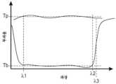
도 8은 반사 편광기의 투과율의 개략 플롯이다.
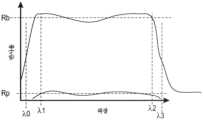
도 9는 반사 편광기의 반사율의 개략 플롯이다.Figure 1a is a schematic perspective drawing of a multilayer optical film.
Figure 1b is a schematic perspective view of a portion of the multilayer optical film of Figure 1a.
FIG. 2a is a schematic side view of an optical stack including first and second reflective polarizers.
Figure 2b is a schematic plan view of the optical stack of Figure 2a.
Figure 3 is a schematic diagram of the layer thickness profile of the optical stack.
Figure 4 is a schematic cross-sectional diagram of the optical structure.
Figure 5 is a schematic side view of a polarizing beam splitter.
Figures 6a to 6c are schematic cross-sectional views of the optical system.
Figure 7 is a schematic cross-sectional diagram of a reflective polarizer (1300).
Figure 8 is a schematic plot of the transmittance of a reflective polarizer.
Figure 9 is a schematic plot of the reflectivity of the reflective polarizer.
하기 설명에서, 본 명세서의 일부를 이루고 다양한 실시예들이 예시로서 도시되어 있는 첨부 도면을 참조한다. 도면은 반드시 일정한 축척으로 작성된 것은 아니다. 다른 실시예가 고려되며 본 명세서의 범주 또는 사상으로부터 벗어남이 없이 이루어질 수 있다는 것이 이해되어야 한다. 따라서, 하기의 상세한 설명은 제한적인 의미로 해석되어서는 안된다.In the following description, reference is made to the accompanying drawings, which form a part of this specification and in which are shown by way of illustration various embodiments. The drawings are not necessarily to scale. It is to be understood that other embodiments are contemplated and may be made without departing from the scope or spirit of the present specification. Accordingly, the following detailed description should not be construed in a limiting sense.
일부 실시예에서, 함께 접착된 제1 및 제2 반사 편광기를 포함하는 광학 스택이 제공된다. 제1 및 제2 반사 편광기는 전형적으로 동일한 미리결정된 파장 범위에서 차단 편광 상태를 반사하도록 구성된 다층 중합체 광학 필름이다. 일부 경우에서, 반사 편광기들 중 하나는 더 낮은 차단 상태 누설을 갖고, 반사 편광기들 중 다른 하나는 반사 하에서 더 낮은 색 분리(color separation)를 갖는다. 예를 들어, 더 낮은 차단 상태 누설을 제공하기 위해 (예를 들어, 각각의 패킷이 동일한 미리결정된 파장 범위 전체에 걸쳐 차단 상태를 반사하도록 구성되는 간섭 층들의 하나 초과의 패킷을 갖는) 더 두꺼운 반사 편광기가 사용될 수 있고, 예를 들어, 일치하는 광 경로들을 따라 반사 편광기에 비스듬히 입사하는 청색 광 및 적색 광의 광 경로들 사이의 더 작은 간격을 생성하기 위해 더 얇은 반사 편광기가 사용될 수 있다. 본 명세서의 광학 스택은 편광 빔 스플리터 및 디스플레이 응용을 포함하는 다양한 응용에 유용하다. 일부 실시예에서, 광학 구조물은 2개의 광학 요소들 사이에 배치되고 이들에 접착된 광학 스택을 포함한다. 광학 요소는 예를 들어 프리즘 또는 렌즈일 수 있다. 일부 실시예에서, 광학 스택을 포함하는 편광 빔 스플리터(PBS)가 제공된다. PBS는 디스플레이 또는 다른 응용에서 사용될 수 있다. 일부 실시예에서, 광학 시스템은, 더 두껍고/두껍거나 더 낮은 차단 상태 누설을 갖는 반사 편광기가 광원에 대면하도록 그리고 더 얇고/얇거나 더 낮은 색 수차를 갖는 반사 편광기가 이미저에 대면하게 배치되도록 배치된 광학 스택을 갖는 PBS를 포함한다. 그러한 광학 시스템은 예를 들어 헤드 마운트 디스플레이 또는 피코 프로젝터에 유용한 것으로 밝혀졌다.In some embodiments, an optical stack is provided that includes first and second reflective polarizers bonded together. The first and second reflective polarizers are typically multilayer polymer optical films configured to reflect a blocking polarization state over the same predetermined wavelength range. In some cases, one of the reflective polarizers has lower blocking state leakage and the other of the reflective polarizers has lower color separation under reflection. For example, a thicker reflective polarizer (e.g., having more than one packet of interference layers, each packet being configured to reflect a blocking state over the same predetermined wavelength range) may be used to provide lower blocking state leakage, and a thinner reflective polarizer may be used to create a smaller gap between the optical paths of blue light and red light incident obliquely on the reflective polarizer along coincident optical paths. The optical stacks of the present disclosure are useful in a variety of applications, including polarizing beam splitters and display applications. In some embodiments, the optical structure includes an optical stack disposed between and bonded to two optical elements. The optical elements may be, for example, prisms or lenses. In some embodiments, a polarizing beam splitter (PBS) comprising an optical stack is provided. The PBS may be used in a display or other application. In some embodiments, the optical system includes a PBS having an optical stack arranged such that a reflective polarizer having a thicker and/or lower blocking state leakage faces the light source and a reflective polarizer having a thinner and/or lower chromatic aberration faces the imager. Such optical systems have been found to be useful in, for example, head mounted displays or pico projectors.
일부 실시예에서, 본 명세서에 기술된 반사 편광기는 미리결정된 파장 범위 내에서 광을 선택적으로 투과시키고 반사하도록 구성된 복수의 광학 층(예컨대, 간섭 층)을 갖는 다층 광학 필름으로서 특성화될 수 있다. 일부 그러한 실시예에서, 광학 필름은 상이한 편광 상태들의 광을 선택적으로 투과시키고 반사하는 반사 편광기로서 기능한다. 예를 들어, 도 1a는 총 (N)개의 간섭 층(102)을 갖는 광학 필름(100)을 형성하도록 중심 축을 따라 위치되는 복수의 간섭 층(102)을 포함하는 다층 광학 필름(100)의 일례의 개략 사시도이다. 도 1b는 교번 간섭 층(102a, 102b)을 예시한 광학 필름(100)의 세그먼트의 개략 사시도이다. 도 1a 및 도 1b는 x, y, 및 z 방향을 정의하는 좌표계를 포함한다.In some embodiments, the reflective polarizer described herein can be characterized as a multilayer optical film having a plurality of optical layers (e.g., interference layers) configured to selectively transmit and reflect light within a predetermined wavelength range. In some such embodiments, the optical film functions as a reflective polarizer that selectively transmits and reflects light of different polarization states. For example, FIG. 1A is a schematic perspective view of an example of a multilayer optical film (100) including a plurality of interference layers (102) positioned along a central axis to form an optical film (100) having a total of (N) interference layers (102). FIG. 1B is a schematic perspective view of a segment of the optical film (100) illustrating alternating interference layers (102a, 102b). FIGS. 1A and 1B include a coordinate system defining the x, y, and z directions.
사용 중에, 입사 광(110)에 의해 도시되는, 광학 필름(100)의 주 표면(예컨대, 필름 표면(104))에 입사하는 광은 광학 필름(100)의 제1 층에 들어가서 복수의 간섭 층(102)을 통해 전파되어, 입사 광(110)의 편광 상태에 따라 광학 간섭에 의해 선택된 반사 또는 투과를 겪을 수 있다. 입사 광(110)은 서로 상호 직교하는 제1 편광 상태(a) 및 제2 편광 상태(b)를 포함할 수 있다. 제1 편광 상태(a)는 "통과" 상태로 간주될 수 있는 반면, 제2 편광 상태(b)는 "반사" 또는 "차단" 상태로 간주될 수 있다. 입사 광(110)이 복수의 간섭 층(102)을 통해 전파됨에 따라, 제2 편광 상태(b)에 있는 광의 부분들은 인접한 간섭 층들에 의해 반사되어 광학 필름(100)에 의해 반사되는 제2 편광 상태(b)를 야기할 것인 반면, 제1 편광 상태(a)에 있는 광의 일부는 집합적으로 광학 필름(100)을 통과한다.In use, light incident on a major surface (e.g., film surface (104)) of the optical film (100), as illustrated by incident light (110), enters the first layer of the optical film (100) and propagates through the plurality of interference layers (102) to undergo selective reflection or transmission by optical interference depending on the polarization state of the incident light (110). The incident light (110) may include a first polarization state (a) and a second polarization state (b) that are mutually orthogonal to each other. The first polarization state (a) may be considered a “passing” state, while the second polarization state (b) may be considered a “reflecting” or “blocking” state. As the incident light (110) propagates through the multiple interference layers (102), portions of the light in the second polarization state (b) will be reflected by adjacent interference layers, resulting in the second polarization state (b) being reflected by the optical film (100), while portions of the light in the first polarization state (a) will collectively pass through the optical film (100).
일부 실시예에서, 광학 필름(100)은 입사 광(110)의 제1 및 제2 편광 상태 (a) 및 (b)의 반사율 및 투과율에 관하여 특성화될 수 있다. 예를 들어, 광학 필름(100)을 통해 투과되는 미리결정된 파장에 대한 입사 광(110)의 양은 제1 편광 상태(a)에 대한 광학 투과율(Ta)의 퍼센트 및 제2 편광 상태(b)에 대한 광학 투과율(Tb)의 퍼센트로서 표현될 수 있다. 광학 필름(100)에 의해 반사되는 미리결정된 파장 범위에 대한 입사 광(110)의 양은 제1 편광 상태(a)에 대한 광학 반사율(Ra)의 퍼센트 및 제2 편광 상태(b)에 대한 광학 반사율(Rb)의 퍼센트로서 표현될 수 있다. 주어진 광학 필름에 대해, 투과율, 반사율, 및 예를 들어 흡수로 인한 손실의 합은 미리결정된 파장 범위 내의 광에 대해 100%에 달할 것이다. 일부 실시예에서, 광학 필름(100)은 미리결정된 파장 범위 내의 광에 대해 비교적 낮은 흡광도(absorbance)를 갖는다. 일부 실시예에서, 광학 필름(100)에 의한 입사 광(110)의 비교적 낮은 흡광도는 보다 적은 열이 광학 필름(100) 내에서 발생되도록 하여, 전체적으로 더욱 효율적인 반사 필름으로 이어질 수 있다.In some embodiments, the optical film (100) can be characterized with respect to reflectivity and transmittance of incident light (110) for first and second polarization states (a) and (b). For example, the amount of incident light (110) for a predetermined wavelength transmitted through the optical film (100) can be expressed as a percentage of optical transmittance (Ta) for the first polarization state (a) and a percentage of optical transmittance (Tb) for the second polarization state (b). The amount of incident light (110) for a predetermined wavelength range reflected by the optical film (100) can be expressed as a percentage of optical reflectivity (Ra) for the first polarization state (a) and a percentage of optical reflectivity (Rb) for the second polarization state (b). For a given optical film, the sum of transmittance, reflectance, and loss due to, for example, absorption, will approach 100% for light within a predetermined wavelength range. In some embodiments, the optical film (100) has a relatively low absorbance for light within the predetermined wavelength range. In some embodiments, the relatively low absorbance of incident light (110) by the optical film (100) may allow less heat to be generated within the optical film (100), resulting in an overall more efficient reflective film.
미리결정된 파장 범위는 예를 들어, 가시광(예를 들어, 약 400 내지 700 nm), 가시광의 범위(예를 들어, 약 400 nm, 또는 약 450 nm 내지 약 650 nm, 또는 약 700 nm), 근-적외선(예를 들어, 약 800 내지 1300 nm), 액정 디스플레이 백라이트와 같은 광원의 출력에 기초한 범위(예를 들어, 425 내지 675 nm), 및 비-수직(off normal) 입사에서 원하는 대역폭을 제공하는 것에 기초한 범위(예를 들어, 400 nm 또는 450 nm 내지 1000 nm 또는 1050 nm)를 포함하는 임의의 적합한 파장 범위일 수 있다 일부 실시예에서, 광학 필름(100)은 하나 초과의 미리결정된 파장 범위 내의 상이한 편광 상태의 광, 예컨대 가시광 및 근-적외선을 투과시키고 반사하도록 구성될 수 있다. 예를 들어, 미리결정된 파장 범위는 약 430 nm 내지 약 465 nm의 제1 범위, 약 490 nm 내지 약 555 nm의 제2 범위, 및 약 600 nm 내지 약 665 nm의 제3 범위를 포함할 수 있다. 일부 실시예에서, 광학 필름(100)은, 본 명세서의 다른 곳에서 추가로 기술되는 바와 같이, 복수의 간섭 층을 각각 포함하는 다수의 패킷을 포함할 수 있으며, 여기서 각각의 패킷은 상이한 미리결정된 파장 범위로 지향될 수 있거나 동일한 미리결정된 파장 범위로 지향될 수 있다.The predetermined wavelength range can be any suitable wavelength range, including, for example, visible light (e.g., about 400 to 700 nm), a range within the visible spectrum (e.g., about 400 nm, or about 450 nm to about 650 nm, or about 700 nm), near-infrared (e.g., about 800 to 1300 nm), a range based on the output of a light source, such as a liquid crystal display backlight (e.g., 425 to 675 nm), and a range based on providing a desired bandwidth at off normal incidence (e.g., 400 nm or 450 nm to 1000 nm or 1050 nm). In some embodiments, the optical film (100) can be configured to transmit and reflect light of different polarization states within more than one predetermined wavelength range, such as visible light and near-infrared. For example, the predetermined wavelength ranges can include a first range from about 430 nm to about 465 nm, a second range from about 490 nm to about 555 nm, and a third range from about 600 nm to about 665 nm. In some embodiments, the optical film (100) can include a plurality of packets, each packet including a plurality of interference layers, as further described elsewhere herein, wherein each packet can be directed to a different predetermined wavelength range or can be directed to the same predetermined wavelength range.
일부 실시예에서, 간섭 층은 일련의 2층 단위 셀들 또는 광학 반복 단위들로서 특성화될 수 있다. 각각의 단위 셀의 두께는 미리결정된 파장 범위 내의 목표 파장을 반사하도록 구성될 수 있다. 일부 예에서, 단위 셀에 대한 반사율의 중심 파장은 2층 단위 셀의 광학 두께의 2배에 해당한다. 따라서, 미리결정된 파장 범위(예컨대, 400 내지 700 nm)를 반사하기 위해, 패킷 내의 단위 셀은 좌측 대역-에지로부터 우측 대역-에지까지의 파장을 커버하도록 상이한 두께를 가질 것이다. 층의 광학 두께는 층의 굴절률과 층의 물리적 두께의 곱을 지칭한다. 차단축을 따라 편광된 광을 반사하고 직교 통과축을 따라 편광된 광을 투과시키도록 구성된 광학 필름의 경우에, 광학 두께를 결정하는 데 사용되는 굴절률은 차단축을 따른 굴절률이다. 광학 반복 단위 내의 2개의 층은 동일하거나 대략 동일한 광학 두께를 가질 수 있다. 일부 경우에, 한 쌍의 층 내의 더 높은 굴절률 층의 광학 두께를 그 층 쌍의 총 광학 두께로 나눈 "f-비"에 관하여 광학 반복 단위를 특성화하는 것이 유용하다. 일부 실시예에서, f-비는 약 0.5이다. 0.5의 f-비가 바람직할 수 있는데, 그 이유는 이것이 광학 필름 또는 간섭 층들의 패킷의 1차(일차) 반사 대역의 반사능을 최대화하기 때문이다.In some embodiments, the interference layer may be characterized as a series of two-layer unit cells, or optical repeat units. The thickness of each unit cell may be configured to reflect a target wavelength within a predetermined wavelength range. In some examples, the center wavelength of the reflectivity for the unit cell is twice the optical thickness of the two-layer unit cell. Thus, to reflect a predetermined wavelength range (e.g., 400 to 700 nm), the unit cells within the packet will have different thicknesses to cover wavelengths from the left band-edge to the right band-edge. The optical thickness of a layer refers to the product of the refractive index of the layer and the physical thickness of the layer. For an optical film configured to reflect light polarized along a block axis and transmit light polarized along an orthogonal pass axis, the refractive index used to determine the optical thickness is the refractive index along the block axis. The two layers within an optical repeat unit may have the same or approximately the same optical thickness. In some cases, it is useful to characterize the optical repeat unit in terms of its "f-ratio," which is the optical thickness of the higher index layer within a pair of layers divided by the total optical thickness of that pair of layers. In some embodiments, the f-ratio is about 0.5. An f-ratio of 0.5 may be desirable because it maximizes the reflectivity of the first-order (primary) reflection band of the optical film or packet of interference layers.
일부 실시예에서, 광학 필름(100)은 약 1200개 미만의(N) 간섭 층(102)을 포함하며, 여기서 각각의 간섭 층(102)은 주로 광학 간섭에 의해 입사 광(110)을 반사하거나 투과시킨다. 일부 실시예에서, 광학 필름(100)은 약 1000개 미만, 또는 약 800개 미만, 또는 약 600개 미만, 또는 약 300개 미만의 간섭 층(102)을 포함한다. 1200개 이상의 간섭 층(102)이 광학 필름(100)에 포함될 수 있지만, 일부 경우에, 디스플레이 조립체(예컨대, LCD 디스플레이)의 전체 두께를 감소시키는 것이 많은 응용에서 바람직하기 때문에, 필름의 전체 두께를 감소시키기 위해 보다 적은 총 개수의 층을 사용하여 원하는 광학 성능을 달성하는 것이 바람직할 수 있다. 추가적으로 또는 대안적으로, 보다 적은 총 개수의 간섭 층(102)은 제조 공정의 복잡성을 감소시킬 수 있을 뿐만 아니라, 최종 광학 필름에서의 가변성(예컨대, 차단 또는 통과 상태에서의 스펙트럼 가변성) 또는 생산 오차(예컨대, 층들 사이의 탈편광으로 인한 증가된 차단 상태 투과율, 감소된 통과 상태 투과율)를 도입하는 것에 대한 가능성을 감소시킬 수 있다. 일부 실시예에서, 차단 상태 누설을 감소시키는 것이 요구될 때 더 많은 수의 간섭 층(102)을 포함하는 것이 요구될 수 있다. 일부 실시예에서, 간섭 층(102)의 총 개수 N은 약 50 초과, 또는 약 100 초과, 또는 약 150 초과, 또는 약 200 초과이다. 일부 실시예에서, 광학 스택은 제1 및 제2 광학 필름(100)을 포함한다. 각각의 광학 필름은 이들 범위 중 임의의 범위 내의 총 N개의 간섭 층을 가질 수 있다. 일부 실시예에서, 제1 광학 필름은 제2 광학 필름보다 더 적은 총 개수의 간섭 층을 갖는다.In some embodiments, the optical film (100) includes less than about 1200 (N) interference layers (102), wherein each interference layer (102) primarily reflects or transmits incident light (110) by optical interference. In some embodiments, the optical film (100) includes less than about 1000, or less than about 800, or less than about 600, or less than about 300 interference layers (102). While more than 1200 interference layers (102) may be included in the optical film (100), in some cases, since reducing the overall thickness of a display assembly (e.g., an LCD display) is desirable in many applications, it may be desirable to achieve the desired optical performance using a smaller total number of layers to reduce the overall thickness of the film. Additionally or alternatively, a smaller total number of interference layers (102) may reduce the complexity of the manufacturing process, as well as the potential for introducing variability in the final optical film (e.g., spectral variability in the block or pass state) or manufacturing errors (e.g., increased block state transmission due to depolarization between layers, decreased pass state transmission). In some embodiments, it may be desirable to include a greater number of interference layers (102) when reducing block state leakage is desired. In some embodiments, the total number N of interference layers (102) is greater than about 50, or greater than about 100, or greater than about 150, or greater than about 200. In some embodiments, the optical stack includes first and second optical films (100). Each optical film can have a total number N of interference layers within any of these ranges. In some embodiments, the first optical film has a smaller total number of interference layers than the second optical film.
일부 실시예에서, 광학 필름(100)은 미리결정된 파장 범위 내의 그리고 미리결정된 입사 각도(입사 광선과 표면 법선 사이의 각도; 예를 들어, 0도는 수직 입사에 대응함)에서의 입사광(110)에 대하여, 제1 편광 상태(a)에 대한 약 80% 초과의 평균 광학 투과율(Ta), 직교 제2 편광 상태(b)에 대한 약 90% 초과의 평균 광학 반사율(Rb), 그리고 일부 경우에, 제2 편광 상태(b)에 대한 약 5% 미만의 평균 광학 투과율(Tb)을 갖는다. 일부 실시예에서, Ta는 약 80% 초과, 또는 약 85% 초과, 또는 약 87% 초과, 또는 약 89% 초과이다. 일부 실시예에서, Rb는 약 90% 초과, 또는 약 95% 초과, 또는 약 96% 초과, 또는 약 97% 초과, 또는 약 98% 초과이다. 일부 실시예에서, Tb는 약 5% 미만, 또는 약 4% 미만, 또는 약 3% 미만, 또는 약 2% 미만, 또는 약 1% 미만, 또는 약 0.5% 미만, 또는 약 0.3% 미만, 또는 약 0.2% 미만, 또는 약 0.1% 미만, 또는 약 0.05% 미만, 또는 약 0.04% 미만, 또는 약 0.03% 미만, 또는 약 0.02% 미만, 또는 약 0.01% 미만이다. 일부 실시예에서, 원하는 Ta, Tb 및 Rb는 광학 필름(100) 내의 또는 광학 필름(100)에 포함된 광학 패킷 내의 약 50개 초과, 또는 약 100개 초과이고 약 1200개 미만, 또는 약 600개 미만, 또는 약 300개 미만인 총 간섭 층(102)을 사용하여 달성된다. 비교적 적은 수의 층을 갖는 높은 Rb(예를 들어, 약 90% 초과) 및 낮은 Tb(예를 들어, 약 5% 미만)는, 제2 편광 상태를 갖는 광에 대한 인접한 간섭 층들 사이의 굴절률 차이는 작고(예를 들어, 0.008 미만), 제1 편광 상태를 갖는 광에 대한 인접한 간섭 층들 사이의 굴절률 차이는 크도록(예컨대, 약 0.2 초과), 간섭 층을 위한 재료를 선택하고 필름의 연신율을 제어함으로써 달성될 수 있다. 굴절률은 파장이 특정되지 않은 경우 550 nm의 파장에서의 굴절률인 것으로 간주될 수 있다.In some embodiments, the optical film (100) has, for incident light (110) within a predetermined wavelength range and at a predetermined incidence angle (the angle between the incident light and the surface normal; for example, 0 degrees corresponds to normal incidence), an average optical transmittance (Ta) of greater than about 80% for the first polarization state (a), an average optical reflectance (Rb) of greater than about 90% for the orthogonal second polarization state (b), and, in some cases, an average optical transmittance (Tb) of less than about 5% for the second polarization state (b). In some embodiments, Ta is greater than about 80%, or greater than about 85%, or greater than about 87%, or greater than about 89%. In some embodiments, Rb is greater than about 90%, or greater than about 95%, or greater than about 96%, or greater than about 97%, or greater than about 98%. In some embodiments, Tb is less than about 5%, or less than about 4%, or less than about 3%, or less than about 2%, or less than about 1%, or less than about 0.5%, or less than about 0.3%, or less than about 0.2%, or less than about 0.1%, or less than about 0.05%, or less than about 0.04%, or less than about 0.03%, or less than about 0.02%, or less than about 0.01%. In some embodiments, the desired Ta, Tb and Rb are achieved using a total interference layer (102) greater than about 50, or greater than about 100 and less than about 1200, or less than about 600, or less than about 300 within the optical film (100) or within an optical packet included in the optical film (100). High Rb (e.g., greater than about 90%) and low Tb (e.g., less than about 5%) with relatively few layers can be achieved by selecting materials for the interference layers and controlling the elongation of the film such that the difference in refractive index between adjacent interference layers for light having the second polarization state is small (e.g., less than 0.008) and the difference in refractive index between adjacent interference layers for light having the first polarization state is large (e.g., greater than about 0.2). The refractive index can be considered to be the refractive index at a wavelength of 550 nm if the wavelength is not specified.
일부 실시예에서, 제1 및 제2 중합체 반사 편광기를 포함하는 광학 스택이 제공되며, 여기서 하나 또는 둘 모두의 반사 편광기는 광학 필름(100)에 대응한다. 제1 및 제2 반사 편광기는 동일한 미리결정된 파장 범위에 대한 광학 필름(100)에 대해 기술된 임의의 범위 내의 Ta, Tb 및 Rb를 가질 수 있다. 일부 실시예에서, 제2 반사 편광기는 제1 반사 편광기보다 높은 콘트라스트 비(Ta/Tb)를 갖는다. 이는 더 낮은 누설(더 낮은 Tb)을 갖는 결과일 수 있으며, 이는 제1 반사 편광기보다 제2 반사 편광기에서 더 많은 수 N개의 간섭 층(102)을 사용하는 것으로부터 기인할 수 있다. 일부 실시예에서, 제1 반사 편광기는 제2 반사 편광기보다 실질적으로 더 얇다(예컨대, 20% 이상).In some embodiments, an optical stack is provided comprising first and second polymeric reflective polarizers, wherein one or both reflective polarizers correspond to an optical film (100). The first and second reflective polarizers can have Ta, Tb, and Rb within any of the ranges described for the optical film (100) for the same predetermined wavelength range. In some embodiments, the second reflective polarizer has a higher contrast ratio (Ta/Tb) than the first reflective polarizer. This may result in lower leakage (lower Tb), which may result from using a greater number N of interference layers (102) in the second reflective polarizer than in the first reflective polarizer. In some embodiments, the first reflective polarizer is substantially thinner (e.g., greater than 20%) than the second reflective polarizer.
광학 필름의 투과율은 일반적으로 (주어진 파장, 입사 방향 등의 광에 대한) 투과 광 강도를 입사 광 강도로 나눈 값을 지칭하지만, "외부 투과율" 또는 "내부 투과율"의 면에서 표현될 수 있다. 광학 필름의 외부 투과율은 공기 중에 있을 때의, 그리고 요소의 전방에 있는 공기/요소 계면에서의 프레넬 반사(Fresnel reflection)에 대해 또는 요소의 후방에 있는 요소/공기 계면에서의 프레넬 반사에 대해 어떠한 보정도 하지 않은 광학 필름의 투과율이다. 광학 필름의 내부 투과율은 그의 전방 및 후방 표면에서의 프레넬 반사가 제거되었을 때의 필름의 투과율이다. 전방 및 후방 프레넬 반사의 제거는 계산적으로(예를 들어, 외부 투과율 스펙트럼으로부터 적절한 함수를 감산함으로써), 또는 실험적으로 수행될 수 있다. 많은 유형의 중합체 및 유리 재료들의 경우, 프레넬 반사는 2개의 외측 표면들 각각에서 (수직 또는 거의 수직 입사각에 대해) 약 4 내지 6%이며, 이는 내부 투과율에 비해 외부 투과율에 대한 약 10%의 하향 시프트를 야기한다. 투과율이 본 명세서에서 내부 또는 외부로서 특정되지 않고서 지칭되는 경우, 문맥에 의해 달리 지시되지 않는 한, 투과율은 외부 투과율을 지칭하는 것으로 가정될 수 있다.The transmittance of an optical film generally refers to the transmitted light intensity (for light of a given wavelength, direction of incidence, etc.) divided by the incident light intensity, but may be expressed in terms of "external transmittance" or "internal transmittance". The external transmittance of an optical film is the transmittance of the optical film when in air and without any correction for Fresnel reflection at the air/element interface in front of the element or for Fresnel reflection at the element/air interface in back of the element. The internal transmittance of an optical film is the transmittance of the film when Fresnel reflections at its front and back surfaces are removed. Removal of the front and back Fresnel reflections can be done computationally (e.g., by subtracting an appropriate function from the external transmittance spectrum) or experimentally. For many types of polymers and glass materials, the Fresnel reflection is about 4 to 6% (for normal or near normal incidence) at each of the two outer surfaces, which results in a downward shift of about 10% for the outer transmittance relative to the inner transmittance. When transmittance is referred to herein without being specified as either inner or outer, it is assumed to refer to the outer transmittance, unless the context indicates otherwise.
일부 실시예에서, 광학 필름(100)의 간섭 층(102)은 상이한 굴절률 특성을 보이는 2가지 상이한 중합체 재료의 교번 층(예컨대, 도 1b에 도시된 A 및 B)을 포함한다. 도 1b에 도시된 바와 같이, 광학 필름(100)은 재료 "(A)" 및 재료 "(B)"로 지칭되는 상이한 광학 재료의 교번 층(예를 들어, ABABA. . .)을 포함한다. 본 명세서의 다른 곳에서 추가로 기술되는 바와 같이, 2가지 상이한 재료의 다양한 층은, 층이 함께 압출되어 함께 부착되는 다수의 광학 층(102)(ABABA. . .)을 형성하는 압출/라미네이션 공정을 통해 형성될 수 있다.In some embodiments, the interference layer (102) of the optical film (100) includes alternating layers of two different polymeric materials exhibiting different refractive index characteristics (e.g., A and B as illustrated in FIG. 1B ). As illustrated in FIG. 1B , the optical film (100) includes alternating layers of different optical materials (e.g., ABABA . . . ) referred to as material “(A)” and material “(B)”. As further described elsewhere herein, the various layers of the two different materials can be formed via an extrusion/lamination process in which the layers are extruded together to form multiple optical layers (102) (ABABA . . . ).
일부 실시예에서, 압출 공정 중에, 광학 층(102)은 필름의 다양한 간섭 특성을 부여하기 위해 신장될 수 있다. 예를 들어, A 및 B 광학 재료의 층은 하나의 축(예컨대, X-축)을 따라 (예컨대, 5:1 비 또는 6:1 비로) 신장될 수 있고, 직교 축(예컨대, Y-축)을 따라서는 눈에 띄게 신장되지 않을 수 있다. X, Y 및 Z 축을 따른 굴절률은 A 또는 B 층에 대해 각각 nx, ny, nz로 표시된다. 굴절률은 또한 X, Y 및 Z 축을 따라 각각, A 및 B 층에 대해 각각 n1x, n1y, n1z 및 n2x, n2y, n2z로 표시될 수 있다.In some embodiments, during the extrusion process, the optical layers (102) may be stretched to impart different interference properties to the film. For example, the layers of A and B optical materials may be stretched along one axis (e.g., the X-axis) (e.g., at a 5:1 ratio or a 6:1 ratio) and not appreciably stretched along the orthogonal axis (e.g., the Y-axis). The refractive indices along the X, Y, and Z axes are denoted nx, ny, and nz for the A or B layers, respectively. The refractive indices may also be denoted along the X, Y, and Z axes as n1x, n1y, n1z and n2x, n2y, n2z for the A and B layers, respectively.
A 및 B 층을 형성하기 위해 사용되는 광학 재료의 선택은 신장 공정의 결과로서 필름에 특정 광학 특성을 부여하도록 선택될 수 있다. 예를 들어, 광학 층(102b)을 형성하는 (B) 재료는 신장 공정에 의해 실질적으로 변경되지 않는 공칭 굴절률(예컨대, 1.5 내지 1.6의 n2)을 가질 수 있다. 이와 같이, x 및 y 방향 둘 모두로의 "B" 층(102b)에 대한 굴절률(n2x 및 n2y)은 신장 공정 후에 둘 모두의 방향에 대해 실질적으로 동일할 수 있고, 두께 방향에서의 굴절률(n2z)과 실질적으로 동일할 수 있다. 대조적으로, 광학 층(102a)을 형성하는 (A) 재료는 신장 공정에 의해 변경되는 굴절률을 가질 수 있다. 예를 들어, (A) 재료의 단축 신장 층(102a)은 X-축 또는 신장 방향(120)에서 더 높은 굴절률을 가질 수 있고(예를 들어, 1.8 ≤ n1x ≤ 1.9), 그리고 두께 방향에서의 굴절률(예를 들어, 1.5 ≤ n1z ≤ 1.6)과 실질적으로 동일할 수 있는 Y-축 또는 비-신장 축/방향(122)과 연관된 상이한 굴절률(예를 들어, 1.5 ≤ n1y ≤ 1.6)을 가질 수 있다. 일부 실시예에서, n1y와 n1z 사이의 차이의 절대값은 0.008 미만이고, n1x와 n1y 사이의 차이는 약 0.2 초과이다. 신장 방향으로의 증가된 굴절률로 인해, 재료(A)를 포함하는 층(102a)은 고 굴절률(high index of refraction, HIR) 층(102a)으로 고려될 수 있는 반면, 재료(B)를 포함하는 간섭 층(102b)은 저 굴절률(low index of refraction, LIR) 층(102b)으로 고려될 수 있다. 일부 실시예에서, n2y와 n2z 사이의 차이의 절대값은 0.005 미만이다. 일부 실시예에서, n2x, n2y 및 n2z 각각은 1.5 내지 1.6이다. 일부 실시예에서, 교번 AB 층의 굴절률은 신중한 재료 선택 및 처리 조건에 의해 제어될 수 있다. 일부 실시예에서, 층(102)의 광학 특성은 광학 필름(100)이 비-신장 축(122)에 대해 배향된 미리결정된 파장 범위 내의 입사 광(110)의 제1 편광 상태(a) 성분을 실질적으로 투과시킬 반사 편광기로서의 역할을 하게 하는 반면, 신장 축(120)은 미리결정된 파장 범위 내의 제2 편광 상태(b)의 입사 광(110)의 성분이 광학 간섭을 통해 실질적으로 반사될 반사-축에 해당할 것이다.The selection of optical materials used to form the A and B layers can be selected to impart particular optical properties to the film as a result of the stretching process. For example, the (B) material forming the optical layer (102b) can have a nominal refractive index (e.g., n2 of 1.5 to 1.6) that is substantially unchanged by the stretching process. As such, the refractive indices (n2x and n2y) for the "B" layer (102b) in both the x and y directions can be substantially the same for both directions after the stretching process, and can be substantially the same as the refractive index (n2z) in the thickness direction. In contrast, the (A) material forming the optical layer (102a) can have a refractive index that is altered by the stretching process. For example, the uniaxially elongated layer (102a) of (A) material can have a higher refractive index in the X-axis or elongation direction (120) (e.g., 1.8 ≤ n1x ≤ 1.9), and a different refractive index associated with the Y-axis or non-elongation axis/direction (122) (e.g., 1.5 ≤ n1y ≤ 1.6) that can be substantially the same as the refractive index in the thickness direction (e.g., 1.5 ≤ n1z ≤ 1.6). In some embodiments, the absolute value of the difference between n1y and n1z is less than 0.008, and the difference between n1x and n1y is greater than about 0.2. Due to the increased refractive index in the direction of extension, the layer (102a) comprising material (A) may be considered a high index of refraction (HIR) layer (102a), while the interference layer (102b) comprising material (B) may be considered a low index of refraction (LIR) layer (102b). In some embodiments, the absolute value of the difference between n2y and n2z is less than 0.005. In some embodiments, each of n2x, n2y and n2z is between 1.5 and 1.6. In some embodiments, the refractive index of the alternating AB layers may be controlled by careful material selection and processing conditions. In some embodiments, the optical properties of the layer (102) are such that the optical film (100) will act as a reflective polarizer that will substantially transmit a first polarization state (a) component of incident light (110) within a predetermined wavelength range oriented about the non-stretch axis (122), whereas the stretch axis (120) will correspond to a reflection-axis along which a second polarization state (b) component of incident light (110) within the predetermined wavelength range will substantially be reflected via optical interference.
일부 실시예에서, 광학 필름(100)은 신장 축(120)을 따른 교번하는 HIR 층(102a) 및 LIR 층(102b) 사이의 굴절률들 사이의 차이(즉, Δnx = n1x-n2x)에 의해 특성화될 수 있다. 일부 그러한 실시예에서, 비-신장 축(122)을 따른 교번 HIR 층(102a)과 LIR 층(102b) 사이의 굴절률은 실질적으로 동일할 수 있어서, 비-신장 축(122)에서의 굴절률들 사이의 차이(즉, Δny = n1y-n2y)가 약 0.0이 되게 한다(예를 들어, |Δny|는 약 0.02 미만, 또는 약 0.01 미만, 또는 약 0.005 미만). 일부 예에서, (예를 들어, 재료의 선택 및/또는 필름의 일축 배향의 제어를 통해) HIR 및 LIR 층(102a, 102b) 사이의 Δnx를 증가시키는 것은 동일한 광파워에 대해 보다 낮은 Δnx를 갖는 광학 필름에 비해 보다 적은 총 개수의 간섭 층을 사용하여 주어진 파장 범위에 대해 편광된 광의 충분한 투과/반사를 허용할 수 있다.In some embodiments, the optical film (100) can be characterized by the difference between the refractive indices between the alternating HIR layers (102a) and LIR layers (102b) along the stretch axis (120) (i.e., Δnx = n1x-n2x). In some such embodiments, the refractive indices between the alternating HIR layers (102a) and LIR layers (102b) along the non-stretch axis (122) can be substantially identical such that the difference between the refractive indices along the non-stretch axis (122) (i.e., Δny = n1y-n2y) is about 0.0 (e.g., |Δny| is less than about 0.02, or less than about 0.01, or less than about 0.005). In some examples, increasing the Δnx between the HIR and LIR layers (102a, 102b) (e.g., via selection of materials and/or control of the uniaxial orientation of the films) may allow sufficient transmission/reflection of polarized light for a given wavelength range using a smaller total number of interference layers compared to an optical film with a lower Δnx for the same optical power.
바람직하게는, 간섭 층(102) 각각의 신장 방향/축은, 각자의 층(102) 각각에 대한 X-축이 각각의 층에 대해 X-Y 평면 내에서 최대 굴절률을 얻기 위한 방향을 나타내도록, 실질적으로 정렬(예컨대, 정렬 또는 거의 정렬)될 것이다. 그러나, 기계 공차 및 간섭 층(102)의 개수로 인해, (예컨대, 층에 대한 최대 굴절률을 얻는 방향을 나타내는) 간섭 층들 각각에 대한 신장 축(120)은 약 ±2°의 분산(variance) 내로 정렬될 수 있다.Preferably, the elongation direction/axis of each of the interference layers (102) will be substantially aligned (e.g., aligned or nearly aligned) such that the X-axis for each of the respective layers (102) represents the direction for achieving maximum refractive index within the X-Y plane for each layer. However, due to mechanical tolerances and the number of interference layers (102), the elongation axes (120) for each of the interference layers (e.g., representing the direction for achieving maximum refractive index for the layer) may be aligned within a variance of about ±2°.
일부 실시예에서, 인접한 제1 및 제2 층(102a, 102b)의 각각의 쌍에 대해, 층들은 각자의 층에 대해 최대 굴절률이 얻어진 방향을 나타내는 신장 축을 한정할 수 있다(예컨대, X-축/방향(120)은 2개의 층에 대한 굴절률 n1x 및 n2x에 대응함). 주 축(primary axis)에 대한 제1 층(102a)과 제2 층(102b) 사이의 굴절률의 차이(예컨대, Δnx = n1x-n2x)는 약 0.2 초과 또는 약 0.24 초과일 수 있다.In some embodiments, for each pair of adjacent first and second layers (102a, 102b), the layers can define an elongation axis representing a direction along which a maximum refractive index is obtained for each layer (e.g., the X-axis/direction (120) corresponds to refractive indices n1x and n2x for the two layers). The difference in refractive indices between the first layer (102a) and the second layer (102b) with respect to the primary axis (e.g., Δnx = n1x-n2x) can be greater than about 0.2 or greater than about 0.24.
복수의 간섭 층(102)을 포함하는 광학 필름(100)은 임의의 적합한 기술을 사용하여 형성될 수 있다. 다층 광학 필름을 형성하기 위한 일반적인 기술은 미국 특허 제5,882,774호(Jonza 등) "Optical Film", 미국 특허 제6,179,948호(Merrill 등) "Optical Film and Process for Manufacture Thereof", 미국 특허 제6,783,349호(Neavin 등) "Apparatus for Making Multilayer Optical Films", 및 미국 특허 출원 공개 제2011/0272849호(Neavin 등) "Feedblock for Manufacturing Multilayer Polymeric Films"에 기술되어 있다. 예를 들어, 각각 광학 재료 A 및 B를 포함하는 층(102a, 102b)은 공압출, 캐스팅, 및 배향 공정을 사용하여 수십 내지 수백 개의 간섭 층(102)의 패킷을 형성한 후에, 압출된 층을 신장 또는 달리 배향시켜 간섭 층(102)의 패킷을 형성하여 제조될 수 있다. 각각의 패킷은 광학 필름(100)의 원하는 특성에 따라 약 200개 내지 1000개의 총 간섭 층을 포함할 수 있다. 본 명세서에 사용되는 바와 같이, "패킷"은 패킷 내에 형성된(예컨대, 순차적으로 배열된) 임의의 스페이서 또는 비-간섭 층이 없는 교번 간섭 층(102a, 102b)의 연속 세트를 지칭하는 데 사용된다. 일부 실시예에서, 스페이서, 비-간섭 층, 또는 다른 층이 주어진 패킷의 외부에 추가되어서, 패킷 내의 간섭 층(102)의 교번 패턴을 붕괴시킴이 없이 필름의 외측 층을 형성할 수 있다.The optical film (100) including a plurality of interference layers (102) can be formed using any suitable technique. General techniques for forming multilayer optical films are described in U.S. Pat. No. 5,882,774 (Jonza et al.), “Optical Film,” U.S. Pat. No. 6,179,948 (Merrill et al.), “Optical Film and Process for Manufacture Thereof,” U.S. Pat. No. 6,783,349 (Neavin et al.), “Apparatus for Making Multilayer Optical Films,” and U.S. Patent Application Publication No. 2011/0272849 (Neavin et al.), “Feedblock for Manufacturing Multilayer Polymeric Films.” For example, layers (102a, 102b), each including optical materials A and B, can be manufactured by forming packets of tens to hundreds of interference layers (102) using coextrusion, casting, and orienting processes, and then stretching or otherwise orienting the extruded layers to form packets of interference layers (102). Each packet can include about 200 to about 1000 total interference layers, depending on the desired properties of the optical film (100). As used herein, "packet" is used to refer to a continuous set of alternating interference layers (102a, 102b) without any spacers or non-interfering layers formed (e.g., arranged sequentially) within the packet. In some embodiments, spacers, non-interfering layers, or other layers may be added to the exterior of a given packet to form outer layers of the film without disrupting the alternating pattern of interference layers (102) within the packet.
일부 실시예에서, 광학 필름(100)은 공압출에 의해 제조될 수 있다. 제조 방법은 (a) 완성된 필름에 사용될 제1 및 제2 중합체에 대응하는 수지의 적어도 제1 및 제2 스트림을 제공하는 단계; (b) (i) 제1 및 제2 유동 채널을 포함하는 구배 플레이트 - 여기서, 제1 채널은 유동 채널을 따라 제1 위치로부터 제2 위치로 변화하는 단면적을 가짐 -, (ii) 제1 유동 채널과 유체 연통하는 제1 복수의 도관 및 제2 유동 채널과 유체 연통하는 제2 복수의 도관을 구비한 피더 튜브 플레이트(feeder tube plate) - 각각의 도관은 그 자신의 각자의 슬롯 다이(slot die)에 공급하고, 각각의 도관은 제1 단부와 제2 단부를 가지며, 도관의 제1 단부는 유동 채널과 유체 연통하고, 도관의 제2 단부는 슬롯 다이와 유체 연통함 -, 및 (iii) 선택적으로, 상기 도관들에 근접 위치된 축방향 로드 히터(axial rod heater)를 포함하는 것과 같은, 적합한 피드블록을 사용하여 제1 및 제2 스트림을 복수의 층으로 분할하는 단계; (c) 각각의 층이 인접한 층들의 주 표면에 대체로 평행한 다층 웨브를 형성하기 위해 복합 스트림을 압출 다이에 통과시키는 단계; 및 (d) 때로는 캐스팅 휠 또는 캐스팅 드럼으로 지칭되는 냉각 롤 상에 다층 웨브를 캐스팅하여, 캐스팅된 다층 필름을 형성하는 단계를 포함할 수 있다. 이러한 캐스팅된 필름은 완성된 필름과 동일한 수의 층을 가질 수 있지만, 캐스팅된 필름의 층은 전형적으로 완성된 필름의 층보다 훨씬 더 두껍다.In some embodiments, the optical film (100) may be manufactured by coextrusion. The manufacturing method comprises the steps of: (a) providing at least first and second streams of resin corresponding to first and second polymers to be used in the finished film; (b) (i) a gradient plate comprising first and second flow channels, wherein the first channel has a cross-sectional area that varies from a first position to a second position along the flow channels, (ii) a feeder tube plate having a first plurality of conduits in fluid communication with the first flow channels and a second plurality of conduits in fluid communication with the second flow channels, each conduit feeding its own respective slot die, each conduit having a first end and a second end, the first end of the conduit being in fluid communication with the flow channels and the second end of the conduit being in fluid communication with the slot die, and (iii) optionally, splitting the first and second streams into a plurality of layers using a suitable feedblock, such as one comprising an axial rod heater positioned proximate to the conduits; (c) passing the composite stream through an extrusion die to form a multilayer web, each layer being generally parallel to a major surface of adjacent layers; and (d) casting the multilayer web onto a cooling roll, sometimes referred to as a casting wheel or casting drum, to form a cast multilayer film. The cast film may have the same number of layers as the finished film, but the layers of the cast film are typically much thicker than the layers of the finished film.
냉각 후에, 다층 웨브는 거의-완성된 다층 광학 필름을 생성하기 위해 재가열 및 연신 또는 신장될 수 있다. 연신 또는 신장은 2가지 목표를 달성하는데, 즉 그것은 층들을 그들의 원하는 최종 두께 프로파일로 박화하고, 그것은 층들 중 적어도 일부가 복굴절성이 되도록 층들을 배향시킨다. 배향 또는 신장은 (예컨대, 텐터(tenter)를 통해) 웨브-횡단 방향(cross-web direction)을 따라, (예컨대, 길이 배향기(length orienter)를 통해) 웨브-하류 방향(down-web direction)을 따라, 또는, 동시에든지 또는 순차적으로든지 간에, 이들의 임의의 조합으로 달성될 수 있다. 하나의 방향만을 따라 신장되는 경우, 신장은 "비구속"되거나(여기서 필름은 신장 방향에 수직인 평면내 방향으로 치수적으로 이완되도록 허용됨) "구속"될 수 있다(여기서 필름은 구속되며 이에 따라 신장 방향에 수직인 평면내 방향으로 치수적으로 이완되도록 허용되지 않음). 둘 모두의 평면내 방향을 따라 신장된다면, 신장은 대칭적이거나, 즉 직교하는 평면내 방향들을 따라 동일하거나, 비대칭적일 수 있다. 대안적으로, 필름은 배치 공정(batch process)으로 신장될 수 있다. 어떤 경우에도, 후속적인 또는 동시적인 연신 감소, 응력 또는 변형 평형, 열 고정(heat setting), 및 다른 처리 작업이 또한 필름에 적용될 수 있다.After cooling, the multilayer web can be reheated and stretched or elongated to produce a nearly-finished multilayer optical film. Stretching or elongation accomplishes two goals: it thins the layers to their desired final thickness profile, and it orients the layers so that at least some of the layers are birefringent. The orientation or elongation can be accomplished along the cross-web direction (e.g., via a tenter), along the down-web direction (e.g., via a length orienter), or any combination thereof, either simultaneously or sequentially. When elongation is along only one direction, the elongation can be "unconstrained" (wherein the film is allowed to relax dimensionally in the in-plane direction perpendicular to the elongation direction) or "constrained" (wherein the film is constrained and thus not allowed to relax dimensionally in the in-plane direction perpendicular to the elongation direction). If stretched along both in-plane directions, the stretch may be symmetrical, i.e., equal along the orthogonal in-plane directions, or asymmetrical. Alternatively, the film may be stretched in a batch process. In either case, subsequent or simultaneous stretch reduction, stress or strain equilibration, heat setting, and other processing operations may also be applied to the film.
다양한 층들의 중합체들은 바람직하게는 유사한 리올로지 특성, 예를 들어 용융 점도를 갖도록 선택되어, 그것들은 상당한 유동 교란 없이 공압출될 수 있다. 압출 조건은 각자의 중합체를 공급 스트림 또는 용융 스트림으로서 연속적이고 안정된 방식으로 적절히 공급, 용융, 혼합 및 펌핑하도록 선택될 수 있다. 용융 스트림들 각각을 형성 및 유지하는 데 사용되는 온도는, 온도 범위의 하한에서 동결, 결정화, 또는 과도하게 높은 압력 강하를 회피하고, 그 범위의 상한에서 재료 열화를 회피하는 범위 내에 있도록 선택될 수 있다.The polymers of the various layers are preferably selected to have similar rheological properties, e.g., melt viscosities, so that they can be coextruded without significant flow disturbances. The extrusion conditions can be selected to suitably feed, melt, mix and pump each of the polymers as a feed stream or a melt stream in a continuous and stable manner. The temperatures used to form and maintain each of the melt streams can be selected to fall within a range that avoids freezing, crystallization, or excessively high pressure drops at the lower end of the temperature range, and that avoids material degradation at the upper end of the range.
광학 필름(100)에 적합한 예시적인 (A) 재료는 예를 들어 폴리에틸렌 나프탈레이트(PEN), PEN 및 폴리에스테르를 함유하는 공중합체(예컨대, 폴리에틸렌 테레프탈레이트(PET) 또는 디벤조산), 글리콜 개질 폴리에틸렌 테레프탈레이트를 포함할 수 있다. 광학 필름(100)에 적합한 예시적인 (B) 재료는 예를 들어 PEN에 기반한 코폴리에스테르, PET에 기반한 코폴리에스테르, 폴리카르보네이트(PC), 또는 이들 3가지 부류의 재료의 블렌드를 포함할 수 있다. 적정한 수의 층들로 높은 반사율을 달성하기 위하여, 인접한 미세층들이 x-축을 따라 편광된 광에 대해 예를 들어, 적어도 0.2의 굴절률 차이(Δnx)를 보일 수 있다.Exemplary (A) materials suitable for the optical film (100) can include, for example, polyethylene naphthalate (PEN), copolymers containing PEN and polyester (e.g., polyethylene terephthalate (PET) or dibenzoic acid), glycol modified polyethylene terephthalate. Exemplary (B) materials suitable for the optical film (100) can include, for example, copolyesters based on PEN, copolyesters based on PET, polycarbonate (PC), or blends of these three classes of materials. To achieve high reflectivity with an appropriate number of layers, adjacent microlayers can exhibit a refractive index difference (Δnx) of, for example, at least 0.2 for light polarized along the x-axis.
일부 실시예에서, 광학 필름(100)은 임의의 선택적인 비-간섭 또는 보호 층을 포함하여 광학 필름(100)에 대한 전체 두께가 약 100 μm 미만인 약 100개 내지 약 1200개의 총 간섭 층(102)을 구비할 수 있다. 일부 실시예에서, 광학 필름(100)은 광학 필름(100)의 모든 층에 걸쳐 약 100 μm 미만(예컨대, 90 μm 미만 또는 50 μm 내지 90 μm의 범위)의 총 두께를 갖는다. 일부 실시예에서, 광학 스택은 제2 광학 필름(100)에 접착된 제1 광학 필름(100)을 포함하며, 여기서 각각의 광학 필름은 반사 편광기이다. 일부 실시예에서, 제1 반사 편광기는 약 50 μm 미만보다 대략 미만(예컨대, 20 μm 내지 45 μm의 범위)의 두께를 갖고, 제2 반사 편광기는 제1 반사 편광기의 두께보다 크고 약 100 μm 미만(예를 들어, 55 μm 내지 95 μm의 범위)의 두께를 갖는다.In some embodiments, the optical film (100) can have from about 100 to about 1200 total interference layers (102) having an overall thickness of less than about 100 μm across all layers of the optical film (100), including any optional non-interference or protective layers. In some embodiments, the optical film (100) has a total thickness of less than about 100 μm (e.g., less than 90 μm or in a range of 50 μm to 90 μm) across all layers of the optical film (100). In some embodiments, the optical stack comprises a first optical film (100) adhered to a second optical film (100), wherein each optical film is a reflective polarizer. In some embodiments, the first reflective polarizer has a thickness of approximately less than about 50 μm (e.g., in the range of 20 μm to 45 μm) and the second reflective polarizer has a thickness greater than the thickness of the first reflective polarizer and less than about 100 μm (e.g., in the range of 55 μm to 95 μm).
일부 실시예에서, 개별 간섭 층(102)의 두께는 간섭 층(102)의 30% 미만이 약 200 nm보다 큰 두께를 갖도록(예컨대, 간섭 층(102)의 5% 미만이 200 nm보다 큰 두께를 가질 수 있거나, 모든 간섭 층(102)이 약 200 nm 미만의 두께를 가질 수 있음) 비교적 얇을 수 있지만, 광학 필름(100) 내에서의 위치의 함수로서 달라질 수 있다. 일부 예에서, 광학 필름(100)은 필름의 두께 프로파일에 관하여 특성화될 수 있다. 예를 들어, 개별 간섭 층(102)의 두께는, 개별 간섭 층(102)의 두께가 일반적으로 최외측 간섭 층으로부터 광학 필름(100)의 중심 근처 또는 반대편 면 근처의 간섭 층으로 이동하면서 증가하도록(예컨대, 국소 변동 외에 증가하는 두께) 달라질 수 있다. 일부 실시예에서, 간섭 층(102)의 30% 미만이 약 45 nm 미만의 두께를 갖는다(예컨대, 간섭 층(102)의 5% 미만이 45 nm 미만의 두께를 가질 수 있거나, 모든 간섭 층(102)이 약 45 nm 미만의 두께를 가질 수 있다).In some embodiments, the thickness of an individual interference layer (102) may be relatively thin, such that less than 30% of the interference layers (102) have a thickness greater than about 200 nm (e.g., less than 5% of the interference layers (102) may have a thickness greater than 200 nm, or all of the interference layers (102) may have a thickness less than about 200 nm), but may vary as a function of location within the optical film (100). In some examples, the optical film (100) may be characterized with respect to a thickness profile of the film. For example, the thickness of an individual interference layer (102) may vary such that the thickness of the individual interference layer (102) generally increases from the outermost interference layer toward the center or near the opposite side of the optical film (100) (e.g., increases in thickness in addition to localized variations). In some embodiments, less than 30% of the interference layer (102) has a thickness less than about 45 nm (e.g., less than 5% of the interference layer (102) can have a thickness less than 45 nm, or all of the interference layer (102) can have a thickness less than about 45 nm).
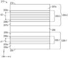
도 2a는 제1 및 제2 반사 편광기(200-1, 200-2)를 포함하는 광학 스택(210)의 개략 단면도이다. 제1 반사 편광기(200-1)는 복수의 중합체 간섭 층(202-1)을 포함하고, 제2 반사 편광기(200-2)는 복수의 중합체 간섭 층(202-2)을 포함한다. 예시의 용이함을 위해 비교적 적은 수의 간섭 층이 도시되어 있지만, 제1 및 제2 반사 편광기(200-1, 200-2) 각각은 더 많은 층을 포함할 수 있다는 것이 이해될 것이다. 복수의 중합체 간섭 층(202-1)은 서로 가장 먼 2개의 중합체 간섭 층(203a, 206a)을 포함한다. 2개의 중합체 간섭 층(203a, 206a)은 거리(d1)만큼 분리된다. 복수의 중합체 간섭 층(202-2)은 서로 가장 먼 2개의 중합체 간섭 층(203b, 206b)을 포함한다. 2개의 중합체 간섭 층(203b, 206b)은 거리(d2)만큼 분리된다. 일부 실시예에서, d1은 d2보다 20% 이상 더 작다. 다시 말하면, d1이 (1-P)와 d2의 곱으로 표현되는 경우, P는 0.2 이상이다. 일부 실시예에서, d1 ≤ 0.8 d2, 또는 d1 ≤ 0.7 d2, 또는 d1 ≤ 0.6 d2이다. 일부 실시예에서, d1 ≥ 0.05 d2, 또는 d1 ≥ 0.1 d2이다. 일부 실시예에서, d1은 500 nm 이상, 또는 1 마이크로미터 이상, 또는 2 마이크로미터 이상, 또는 5 마이크로미터 이상, 또는 10 마이크로미터 이상, 또는 20 마이크로미터 이상이다. 일부 실시예에서, d2는 250 마이크로미터 이하, 또는 200 마이크로미터 이하, 또는 150 마이크로미터 이하, 또는 100 마이크로미터 이하이다. 일부 실시예에서, d2는 50 마이크로미터 이상, 또는 55 마이크로미터 이상, 또는 60 마이크로미터 이상이다. 일부 실시예에서, d1은 50 마이크로미터 미만, 또는 45 마이크로미터 미만, 또는 40 마이크로미터 미만이다. 예를 들어, 일부 실시예에서, d1은 20 마이크로미터 내지 40 마이크로미터의 범위이고, d2는 50 마이크로미터 내지 200 마이크로미터의 범위이다.FIG. 2a is a schematic cross-sectional view of an optical stack (210) including first and second reflective polarizers (200-1, 200-2). The first reflective polarizer (200-1) includes a plurality of polymer interference layers (202-1), and the second reflective polarizer (200-2) includes a plurality of polymer interference layers (202-2). Although a relatively small number of interference layers are shown for ease of illustration, it will be appreciated that each of the first and second reflective polarizers (200-1, 200-2) may include more layers. The plurality of polymer interference layers (202-1) includes two polymer interference layers (203a, 206a) that are furthest from each other. The two polymer interference layers (203a, 206a) are separated by a distance (d1). The plurality of polymer interference layers (202-2) include two polymer interference layers (203b, 206b) that are furthest from each other. The two polymer interference layers (203b, 206b) are separated by a distance (d2). In some embodiments, d1 is at least 20% smaller than d2. In other words, when d1 is expressed as the product of (1-P) and d2, P is at least 0.2. In some embodiments, d1 ≤ 0.8 d2, or d1 ≤ 0.7 d2, or d1 ≤ 0.6 d2. In some embodiments, d1 ≥ 0.05 d2, or d1 ≥ 0.1 d2. In some embodiments, d1 is at least 500 nm, or at least 1 micrometer, or at least 2 micrometers, or at least 5 micrometers, or at least 10 micrometers, or at least 20 micrometers. In some embodiments, d2 is less than or equal to 250 micrometers, or less than or equal to 200 micrometers, or less than or equal to 150 micrometers, or less than or equal to 100 micrometers. In some embodiments, d2 is greater than or equal to 50 micrometers, or greater than or equal to 55 micrometers, or greater than or equal to 60 micrometers. In some embodiments, d1 is less than or equal to 50 micrometers, or less than or equal to 45 micrometers, or less than 40 micrometers. For example, in some embodiments, d1 is in the range of 20 micrometers to 40 micrometers, and d2 is in the range of 50 micrometers to 200 micrometers.
제1 반사 편광기(200-1)는 비간섭 층(205a, 205b)을 포함하고, 제2 반사 편광기(200-2)는 비간섭 층(207a, 207b)을 포함한다. 이들 비간섭 층은 반사 편광기가 형성될 때 반사 편광기와 함께 포함된 스킨 층 또는 보호 경계 층일 수 있다.The first reflective polarizer (200-1) includes an incoherent layer (205a, 205b), and the second reflective polarizer (200-2) includes an incoherent layer (207a, 207b). These incoherent layers may be skin layers or protective boundary layers included together with the reflective polarizer when the reflective polarizer is formed.
간섭 층은, 간섭 층의 반사율 및 투과율이 광학 간섭에 의해 합리적으로 기술될 수 있거나 또는 광학 간섭으로부터 야기되는 것으로 합리적으로 정확하게 모델링될 수 있을 때 주로 광학 간섭에 의해 광을 반사하고 투과시키는 것으로 기술될 수 있다. 상이한 굴절률을 갖는 간섭 층의 인접한 쌍은, 그 쌍이, 조합된 광학 두께(차단 축을 따른 굴절률 x 물리적 두께)가 광의 파장의 1/2일 때 광학 간섭에 의해 광을 반사한다. 간섭 층은 전형적으로 물리적 두께가 약 200 나노미터 미만이다. 일부 실시예에서, 각각의 중합체 간섭 층은 약 45 나노미터 내지 약 200 나노미터 범위의 평균 두께(층 위의 물리적 두께의 비가중 평균)를 갖는다. 비간섭 층은, 간섭을 통한 가시광의 반사에 기여하기에는 너무 큰 광학 두께를 갖는다. 비간섭 층은 전형적으로 물리적 두께가 1 마이크로미터 이상, 또는 5 마이크로미터 이상이다. 비간섭 층(205a, 205b, 207a, 207b)은 주로 광학 간섭에 의해 광을 반사하거나 투과시키지 않는다.An interference layer may be described as reflecting and transmitting light primarily by optical interference when the reflectivity and transmittance of the interference layer can be reasonably described by optical interference, or can be reasonably accurately modeled as resulting from optical interference. Adjacent pairs of interference layers having different refractive indices reflect light by optical interference when the pair has a combined optical thickness (refractive index along the blocking axis times the physical thickness) equal to half the wavelength of the light. The interference layers typically have a physical thickness of less than about 200 nanometers. In some embodiments, each polymeric interference layer has an average thickness (an unweighted average of the physical thicknesses over the layers) in the range of about 45 nanometers to about 200 nanometers. The incoherent layers have an optical thickness that is too large to contribute to reflection of visible light via interference. The incoherent layers typically have a physical thickness of greater than or equal to 1 micrometer, or greater than or equal to 5 micrometers. The non-interfering layers (205a, 205b, 207a, 207b) do not reflect or transmit light primarily due to optical interference.
광학 스택(210)은 대향하는 최외측 제1 및 제2 주 표면(204, 214)을 가지며, 제1 반사 편광기(200-1)는 제1 주 표면(204)에 더 가깝게 배치되고 제2 주 표면(214)으로부터 더 멀리 배치되고, 제2 반사 편광기(200-2)는 제2 주 표면(214)에 더 가깝게 배치되고 제1 주 표면(204)으로부터 더 멀리 배치된다. 일부 실시예에서, 각각의 반사 편광기 및 반사 편광기에 가장 가까운 주 표면에 대해, 주 표면에 더 가까운 각각의 중합체 간섭 층은 더 작은 광학 두께를 갖고, 주 표면으로부터 더 먼 각각의 간섭 층은 더 큰 광학 두께를 갖는다. 예를 들어, 간섭 층(203a)은 간섭 층(206a)보다 작은 광학 두께를 가질 수 있고, 간섭 층(203b)은 간섭 층(206b)보다 작은 광학 두께를 가질 수 있다.The optical stack (210) has opposing first and second outermost major surfaces (204, 214), wherein the first reflective polarizer (200-1) is positioned closer to the first major surface (204) and further from the second major surface (214), and the second reflective polarizer (200-2) is positioned closer to the second major surface (214) and further from the first major surface (204). In some embodiments, for each reflective polarizer and the major surface closest to the reflective polarizer, each polymeric interference layer closer to the major surface has a smaller optical thickness, and each interference layer farther from the major surface has a larger optical thickness. For example, interference layer (203a) can have a smaller optical thickness than interference layer (206a), and interference layer (203b) can have a smaller optical thickness than interference layer (206b).
광학 스택(210)은 제1 반사 편광기(200-1)와 제2 반사 편광기(200-2) 사이에 중간 층(209)을 포함한다. 일부 실시예에서, 중간 층(209)은 제1 및 제2 반사 편광기(200-1, 200-2)를 함께 접합시키는 접착제 층이다. 일부 실시예에서, 중간 층 (209)은 광학적으로 투명한 접착제 층이다. 광학적으로 투명한 접착제 층은 미리결정된 파장 범위(예컨대, 400 nm 내지 700 nm) 및 5% 미만 또는 3% 미만의 광학 탁도(optical haze)에 걸쳐, 수직 입사에서의 투과율이 80% 이상, 또는 90% 이상일 수 있다. 다른 실시예들에서, 제1 및 제2 반사 편광기(200-1, 200-2)는 일체로 형성될 수 있고, 중간 층(209)은 제1 및 제2 반사 편광기(200-1, 200-2)와 함께 공압출된 중합체 층이다.The optical stack (210) includes an intermediate layer (209) between the first reflective polarizer (200-1) and the second reflective polarizer (200-2). In some embodiments, the intermediate layer (209) is an adhesive layer that bonds the first and second reflective polarizers (200-1, 200-2) together. In some embodiments, the intermediate layer (209) is an optically transparent adhesive layer. The optically transparent adhesive layer can have a transmittance at normal incidence of greater than or equal to 80%, or greater than or equal to 90%, over a predetermined wavelength range (e.g., 400 nm to 700 nm) and an optical haze of less than 5% or less than 3%. In other embodiments, the first and second reflective polarizers (200-1, 200-2) may be formed integrally, and the intermediate layer (209) is a polymer layer co-extruded with the first and second reflective polarizers (200-1, 200-2).
도 2b는 제1 및 제2 반사 편광기(200-1, 200-2)의 통과축(222, 224)을 각각 예시하는 광학 스택(210)의 개략 평면도이다. 통과축(222)과 통과축(224) 사이의 각도(θ)가 도시되어 있다. 일부 실시예에서, 각도(θ)는 약 10도 미만, 또는 약 5도 미만, 또는 약 2도 미만, 또는 약 1도 미만이다.FIG. 2b is a schematic plan view of an optical stack (210) illustrating the pass axes (222, 224) of the first and second reflective polarizers (200-1, 200-2), respectively. The angle (θ) between the pass axes (222) and the pass axes (224) is depicted. In some embodiments, the angle (θ) is less than about 10 degrees, or less than about 5 degrees, or less than about 2 degrees, or less than about 1 degree.
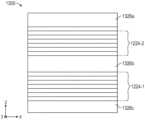
일부 실시예에서, 광학 스택에 포함된 반사 편광기들 중 적어도 하나는 간섭 층들의 하나 초과의 패킷을 포함한다. 도 7은 비간섭 층(1326b)에 의해 분리된 간섭 층들의 제1 및 제2 패킷(1224-1, 1224-2)을 포함하는 반사 편광기(1300)의 개략 단면도이다. 반사 편광기는 외측 비간섭 층(1326a, 1326c)을 추가로 포함한다. 제1 및 제2 패킷(1224-1, 1224-2)은 높은 콘트라스트 비(통과 상태 투과율 대 차단 상태 투과율의 비)를 제공하기 위해 중첩되는 두께 범위를 이용할 수 있다. 일부 실시예에서, 두께 프로파일은 실질적으로 중첩된다(예컨대, 제1 패킷의 두께 범위의 50% 초과가 제2 패킷의 두께 범위의 50% 초과와 중첩된다). 다른 실시예들에서, 두께 범위에서의 중첩이 거의 또는 전혀 없다. 간섭 층들의 하나 초과의 패킷을 포함하는 반사 편광기가 2017년 3월 6일자로 출원된 미국 가특허 출원 제62/467712호(Haag 등)에 추가로 기술되어 있다.In some embodiments, at least one of the reflective polarizers included in the optical stack includes more than one packet of interference layers. FIG. 7 is a schematic cross-sectional view of a reflective polarizer (1300) including first and second packets (1224-1, 1224-2) of interference layers separated by an incoherent layer (1326b). The reflective polarizer further includes an outer incoherent layer (1326a, 1326c). The first and second packets (1224-1, 1224-2) can utilize overlapping thickness ranges to provide a high contrast ratio (ratio of transmittance in the pass state to transmittance in the block state). In some embodiments, the thickness profiles substantially overlap (e.g., greater than 50% of the thickness range of the first packet overlaps greater than 50% of the thickness range of the second packet). In other embodiments, there is little or no overlap in the thickness ranges. A reflective polarizer comprising more than one packet of interference layers is further described in U.S. Provisional Patent Application No. 62/467,712, filed March 6, 2017 (Haag et al.).
제1 및 제2 반사 편광기를 포함하는 광학 스택의 일부 응용의 경우, 제1 반사 편광기는 얇고 제2 반사 편광기는 높은 콘트라스트 비를 갖는 것이 바람직하다. 따라서, 제1 반사 편광기는 간섭 층들의 하나의 패킷을 갖고 제2 반사 편광기는 간섭 층들의 하나 초과의 패킷을 포함하는 것이 바람직할 수 있다. 예를 들어, 반사 편광기(1300)는 광학 스택(210)에서 제2 반사 편광기(200-2)로서 사용될 수 있는 한편, 간섭 층들의 단일 패킷을 포함하는 반사 편광기는 광학 스택(210)에서 제1 반사 편광기(200-1)로서 사용될 수 있다. 전형적으로, 제1 및 제2 반사 편광기 둘 모두는 다층 중합체 필름 반사 편광기이다. 그러나, 일부 경우에, 다른 유형의 반사 편광기(예컨대, 맥네일(MacNeille))가 사용될 수 있다.For some applications of an optical stack including first and second reflective polarizers, it is desirable for the first reflective polarizer to be thin and the second reflective polarizer to have a high contrast ratio. Thus, it may be desirable for the first reflective polarizer to have one packet of interference layers and for the second reflective polarizer to include more than one packet of interference layers. For example, the reflective polarizer (1300) may be used as the second reflective polarizer (200-2) in the optical stack (210), while the reflective polarizer including a single packet of interference layers may be used as the first reflective polarizer (200-1) in the optical stack (210). Typically, both the first and second reflective polarizers are multilayer polymer film reflective polarizers. However, in some cases, other types of reflective polarizers (e.g., MacNeille) may be used.
본 명세서의 반사 편광기는 일체로 형성될 수 있다. 본 명세서에 사용되는 바와 같이, 제2 요소와 "일체로 형성된" 제1 요소란, 제1 및 제2 요소들이 별도로 제조된 후에 후속하여 결합되기보다는 오히려 함께 제조되는 것을 의미한다. 일체로 형성되는 것은, 제1 요소를 제조하는 것, 이어서 제1 요소 상에 제2 요소를 제조하는 것을 포함한다. 복수의 층을 포함하는 광학 필름은, 층들이 별도로 제조된 후 후속하여 결합되기보다는 오히려 함께 제조되는 (예컨대, 용융 스트림으로서 조합되고 이어서 냉각 롤 상으로 캐스팅되어 층들 각각을 갖는 캐스트 필름을 형성하고, 이어서 캐스트 필름을 배향하는) 경우 일체로 형성된다. 일부 실시예에서, 비간섭 층(1326a, 1326c)은 간섭 층의 제1 및 제2 패킷(1224-1, 1224-2) 및 비간섭 층(1326b)과 일체로 형성되어, 반사 편광기(1300)가 일체로 형성되도록 한다.The reflective polarizer of the present disclosure may be integrally formed. As used herein, a first element "integrally formed" with a second element means that the first and second elements are manufactured together, rather than being manufactured separately and then subsequently joined. Integral formation includes manufacturing the first element, followed by manufacturing the second element on the first element. An optical film comprising a plurality of layers is integrally formed when the layers are manufactured together, rather than being manufactured separately and then subsequently joined (e.g., combined as a melt stream and then cast onto a chill roll to form a cast film having each of the layers, and then orienting the cast film). In some embodiments, the non-interfering layers (1326a, 1326c) are integrally formed with the first and second packets (1224-1, 1224-2) of interfering layers and the non-interfering layer (1326b), such that the reflective polarizer (1300) is integrally formed.
도 3은 2개의 반사 편광기를 포함하는 광학 스택(200)과 같은 광학 스택의 층 두께 프로파일의 개략도이다. 제1 반사 편광기는 광학 스택의 최외측 간섭 층에서의 t1로부터 제1 반사 편광기의 최외측 간섭 층 - 이는 제2 반사 편광기에 가장 가까운 광학 스택의 내부 간섭 층임 - 에서의 tm까지의 범위의 두께를 갖는 복수의 중합체 간섭 층(302-1)을 포함한다. 제2 반사 편광기는 제2 반사 편광기의 최외측 간섭 층 - 이는 제1 반사 편광기에 가장 가까운 광학 스택의 내부 간섭 층임 - 에서의 tm+1로부터, 광학 스택의 최외측 간섭 층에서의 tN까지의 범위의 두께를 갖는 복수의 중합체 간섭 층(302-2)을 포함한다. 일부 실시예에서, |t1 - tN|은 약 20 nm 미만, 또는 약 15 nm 미만, 또는 약 12 nm 미만, 또는 약 10 nm 미만, 또는 약 8 nm 미만, 또는 약 7 nm 미만, 또는 약 6 nm 미만이다. 일부 실시예에서, |tm - tm+1|은 약 40 nm 미만, 또는 약 30 nm 미만, 또는 약 20 nm 미만, 또는 약 15 nm 미만, 또는 약 12 nm 미만, 또는 약 10 nm 미만이다.FIG. 3 is a schematic diagram of a layer thickness profile of an optical stack, such as an optical stack (200) including two reflective polarizers. The first reflective polarizer includes a plurality of polymeric interference layers (302-1) having a thickness ranging from t1 at an outermost interference layer of the optical stack to tm at an outermost interference layer of the first reflective polarizer, which is the inner interference layer of the optical stack closest to the second reflective polarizer. The second reflective polarizer includes a plurality of polymeric interference layers (302-2) having a thickness ranging from tm+1 at an outermost interference layer of the second reflective polarizer, which is the inner interference layer of the optical stack closest to the first reflective polarizer, to tN at an outermost interference layer of the optical stack. In some embodiments, |t1 - tN | is less than about 20 nm, or less than about 15 nm, or less than about 12 nm, or less than about 10 nm, or less than about 8 nm, or less than about 7 nm, or less than about 6 nm. In some embodiments, |tm - tm+1 | is less than about 40 nm, or less than about 30 nm, or less than about 20 nm, or less than about 15 nm, or less than about 12 nm, or less than about 10 nm.
도 4는 제1 광학 요소(446)와 제2 광학 요소(448) 사이에 배치되고 이들에 접착된 광학 스택(410)을 포함하는 광학 구조물(450)의 개략 단면도이다. 광학 스택(410)은 접착제(409)와 함께 접착된 제1 및 제2 반사 편광기(400-1, 400-2)를 포함한다. 제1 반사 편광기(400-1)는 제1 광학 요소(446)에 대면하고, 제2 반사 편광기는 제2 광학 요소(448)에 대면한다. 광학 스택(410)은 접착제 층(419)을 이용하여 제1 광학 요소(446)에 접착되고 접착제 층(429)을 이용하여 제2 광학 요소(448)에 접착된다. 제1 및 제2 광학 요소(446, 448)는 임의의 적합한 형상을 가질 수 있다. 일부 실시예에서, 제1 및 제2 광학 요소(446, 448)는 제1 및 제2 프리즘(예컨대, 제1 및 제2 프리즘(530, 540) 또는 제1 및 제2 프리즘(630, 640)에 대응함)이다. 일부 실시예에서, 제1 및 제2 광학 요소(446, 448) 중 하나 또는 둘 모두는 광학 렌즈이다. 광학 스택은 제1 및 제2 광학 요소(446, 448)의 평면인 또는 실질적으로 평면인 면 상에 배치될 수 있거나, 제1 및 제2 광학 요소의 만곡된 면 상에 배치될 수 있다.FIG. 4 is a schematic cross-sectional view of an optical structure (450) including an optical stack (410) disposed between and bonded to a first optical element (446) and a second optical element (448). The optical stack (410) includes first and second reflective polarizers (400-1, 400-2) bonded together with an adhesive (409). The first reflective polarizer (400-1) faces the first optical element (446), and the second reflective polarizer faces the second optical element (448). The optical stack (410) is bonded to the first optical element (446) using an adhesive layer (419) and to the second optical element (448) using an adhesive layer (429). The first and second optical elements (446, 448) may have any suitable shape. In some embodiments, the first and second optical elements (446, 448) are first and second prisms (e.g., corresponding to the first and second prisms (530, 540) or the first and second prisms (630, 640)). In some embodiments, one or both of the first and second optical elements (446, 448) are optical lenses. The optical stack can be disposed on planar or substantially planar surfaces of the first and second optical elements (446, 448), or can be disposed on curved surfaces of the first and second optical elements.
일부 실시예에서, 제1 및 제2 반사 편광기(400-1, 400-2) 각각은 더 짧은 제1 파장으로부터 더 긴 제2 파장으로 연장되는 동일한 미리결정된 파장 범위에서 반사 편광기의 통과축을 따라 편광된 광의 80% 이상을 투과시키고 반사 편광기의 직교 차단축을 따라 편광된 광의 80% 이상을 반사한다. 일부 실시예에서, 제1 파장은 400 nm, 또는 450 nm, 또는 약 400 nm 내지 약 500 nm의 범위, 또는 약 400 nm 내지 약 450 nm의 범위이다. 일부 실시예에서, 제2 파장은 650 nm, 또는 700 nm, 또는 약 600 nm 내지 약 700 nm의 범위, 또는 약 650 nm 내지 약 700 nm의 범위이다. 반사율 및 투과율은 수직 입사와 같은 미리결정된 입사각에서, 또는 45도 입사각에서, 또는 주어진 응용에 대해 적절한 입사각에서 특정될 수 있거나, 반사율 및 투과율은 주어진 응용에서 발생하는 입사각의 분포에 대해 특정될 수 있다.In some embodiments, each of the first and second reflective polarizers (400-1, 400-2) transmits at least 80% of light polarized along a pass axis of the reflective polarizer and reflects at least 80% of light polarized along an orthogonal block axis of the reflective polarizer over the same predetermined wavelength range extending from a shorter first wavelength to a longer second wavelength. In some embodiments, the first wavelength is 400 nm, or 450 nm, or in a range from about 400 nm to about 500 nm, or in a range from about 400 nm to about 450 nm. In some embodiments, the second wavelength is 650 nm, or 700 nm, or in a range from about 600 nm to about 700 nm, or in a range from about 650 nm to about 700 nm. The reflectivity and transmittance can be specified at a predetermined angle of incidence, such as normal incidence, or at a 45 degree angle of incidence, or at an angle of incidence appropriate to a given application, or the reflectivity and transmittance can be specified for a distribution of angles of incidence that occur in a given application.
각자의 제1 및 제2 파장을 갖고 제1 광학 요소(446)의 내부로부터 제1 반사 편광기(400-1)에 대해 45도로 입사하는, 일치하는 제1 및 제2 광선(461a, 462a)은, 제1 광학 요소(446) 내부에서 분리 거리(s1)만큼 서로 이격된 각자의 반사된 제1 및 제2 광선(461b, 462b)으로서 제1 반사 편광기(400-1)에 의해 반사된다. 각자의 제1 및 제2 파장을 갖고 제2 광학 요소(448)의 내부로부터 제2 반사 편광기(400-2)에 대해 45도로 입사하는, 일치하는 제1 및 제2 광선(471a, 472a)은, 제2 광학 요소(448) 내부에서 분리 거리(s2)만큼 서로 이격된 각자의 반사된 제1 및 제2 광선(471b, 472b)으로서 제2 반사 편광기(400-2)에 의해 반사된다.Coinciding first and second light rays (461a, 462a) having their respective first and second wavelengths and incident at 45 degrees to the first reflective polarizer (400-1) from the inside of the first optical element (446) are reflected by the first reflective polarizer (400-1) as respective reflected first and second light rays (461b, 462b) spaced apart from each other by a separation distance (s1) inside the first optical element (446). Coinciding first and second light rays (471a, 472a), each having its own first and second wavelengths, and incident at a 45 degree angle from the inside of the second optical element (448) to the second reflective polarizer (400-2), are reflected by the second reflective polarizer (400-2) as respective reflected first and second light rays (471b, 472b) spaced apart from each other by a separation distance (s2) inside the second optical element (448).
일부 실시예에서, 0 < s1 ≤ s2이다. 일부 실시예에서, s1은 500 nm 초과, 또는 1 마이크로미터 초과, 또는 2 마이크로미터 초과, 또는 5 마이크로미터 초과, 또는 10 마이크로미터 초과이다. 일부 실시예에서, s1은 50 마이크로미터 미만, 또는 30 마이크로미터 미만, 또는 20 마이크로미터 미만, 또는 18 마이크로미터 미만, 또는 16 마이크로미터 미만, 또는 14 마이크로미터 미만, 또는 10 마이크로미터 미만, 또는 8 마이크로미터 미만, 6 마이크로미터 미만, 또는 4 마이크로미터 미만, 또는 2 마이크로미터 미만이다. 예를 들어, 일부 실시예에서, s1은 1 마이크로미터 내지 20 마이크로미터의 범위이다. 일부 실시예에서, s2는 s1 초과, 또는 s1 + 500 nm 초과, 또는 s1 + 1 마이크로미터 초과, 또는 s1 + 2 마이크로미터 초과, 또는 s1 + 5 마이크로미터 초과, 또는 s1 + 10 마이크로미터 초과이다. 일부 실시예에서, s2는 250 마이크로미터 이하, 또는 200 마이크로미터 이하, 또는 150 마이크로미터 이하, 또는 100 마이크로미터 이하이다. 일부 실시예에서, s2는 40 마이크로미터 이상, 50 마이크로미터 이상, 또는 55 마이크로미터 이상, 또는 60 마이크로미터 이상이다.In some embodiments, 0 < s1 ≤ s2. In some embodiments, s1 is greater than 500 nm, or greater than 1 micrometer, or greater than 2 micrometers, or greater than 5 micrometers, or greater than 10 micrometers. In some embodiments, s1 is less than 50 micrometers, or less than 30 micrometers, or less than 20 micrometers, or less than 18 micrometers, or less than 16 micrometers, or less than 14 micrometers, or less than 10 micrometers, or less than 8 micrometers, less than 6 micrometers, or less than 4 micrometers, or less than 2 micrometers. For example, in some embodiments, s1 is in the range of 1 micrometer to 20 micrometers. In some embodiments, s2 is greater than s1, or greater than s1 + 500 nm, or greater than s1 + 1 micrometer, or greater than s1 + 2 micrometers, or greater than s1 + 5 micrometers, or greater than s1 + 10 micrometers. In some embodiments, s2 is less than or equal to 250 micrometers, or less than or equal to 200 micrometers, or less than or equal to 150 micrometers, or less than or equal to 100 micrometers. In some embodiments, s2 is greater than or equal to 40 micrometers, or greater than or equal to 50 micrometers, or greater than or equal to 55 micrometers, or greater than or equal to 60 micrometers.
일부 실시예에서, 각각의 반사 편광기에 대해, 최외측 간섭 층은 제1 및 제2 파장을 각각 반사하도록 구성된다. 일부 그러한 실시예에서, s1은 약 √2 d1이고, 유사하게, s2는 √2 d2이다.In some embodiments, for each reflective polarizer, the outermost interference layer is configured to reflect the first and second wavelengths, respectively. In some such embodiments, s1 is about √2 d1, and similarly, s2 is √2 d2.
도 5는 편광 빔 스플리터(PBS)(550)의 개략 측면도이다. PBS(550)는 제1 빗면(532)을 갖는 제1 프리즘(530), 및 제1 빗면(532)에 대면하는 제2 빗면(542)을 갖는 제2 프리즘(540)을 포함한다. 광학 스택(510)이 각각 제1 및 제2 광학적으로 투명한 접착제 층(534, 544)을 통해 제1 및 제2 빗면(532, 542) 사이에 배치되고 이들에 부착된다. 광학 스택(510)은 광학적으로 투명한 접착제 층(509)을 통해 제2 반사 편광기(500-2)에 접착된 제1 반사 편광기(500-1)를 포함한다. 제1 반사 편광기(500-1)는 제1 빗면(532)에 더 가깝고 제2 빗면(542)으로부터 더 멀고, 제2 반사 편광기(500-2)는 제2 빗면(542)에 더 가깝고 제1 빗면(534)으로부터 더 멀다.FIG. 5 is a schematic side view of a polarizing beam splitter (PBS) (550). The PBS (550) includes a first prism (530) having a first oblique surface (532), and a second prism (540) having a second oblique surface (542) facing the first oblique surface (532). An optical stack (510) is positioned between and attached to the first and second oblique surfaces (532, 542) via first and second optically transparent adhesive layers (534, 544), respectively. The optical stack (510) includes a first reflective polarizer (500-1) bonded to a second reflective polarizer (500-2) via an optically transparent adhesive layer (509). The first reflective polarizer (500-1) is closer to the first oblique plane (532) and farther from the second oblique plane (542), and the second reflective polarizer (500-2) is closer to the second oblique plane (542) and farther from the first oblique plane (534).
일부 실시예에서, 각각의 반사 편광기 및 반사 편광기에 가장 가까운 빗면에 대해: 빗면에 더 가까운 간섭 층은 미리결정된 파장 범위에서 더 짧은 파장을 주로 반사하도록 구성되고, 빗면으로부터 더 먼 간섭 층은 미리결정된 파장 범위에서 더 긴 파장을 주로 반사하도록 구성된다. 예를 들어, 광학 스택(510) 내의 간섭 층들의 두께 프로파일은, 도 3에서 광학 스택의 외측 표면들에 더 가까운 더 얇은 층들(이는 더 짧은 파장을 반사함) 및 광학 스택의 외측 표면들로부터 더 먼 더 두꺼운 층들(이는 더 긴 파장을 반사함)을 갖는 것과 같이 나타날 수 있다.In some embodiments, for each reflective polarizer and the oblique plane closest to the reflective polarizer: the interference layer closer to the oblique plane is configured to primarily reflect shorter wavelengths in the predetermined wavelength range, and the interference layer farther from the oblique plane is configured to primarily reflect longer wavelengths in the predetermined wavelength range. For example, the thickness profile of the interference layers within the optical stack (510) may be represented as having thinner layers closer to the outer surfaces of the optical stack (which reflect shorter wavelengths) and thicker layers farther from the outer surfaces of the optical stack (which reflect longer wavelengths) in FIG. 3 .
일부 실시예에서, PBS(550)는 광학 축(555)을 갖거나, 또는 광학 축(555)을 갖는 광학 시스템에 사용된다. 일부 실시예에서, 광학 축(555)은 광학 스택(510)과 약 30 내지 60도, 또는 약 35 내지 55도, 또는 약 40 내지 50도, 또는 약 45도의 각도(α)를 이룬다.In some embodiments, the PBS (550) has an optical axis (555), or is used in an optical system having an optical axis (555). In some embodiments, the optical axis (555) forms an angle (α) with the optical stack (510) of about 30 to 60 degrees, or about 35 to 55 degrees, or about 40 to 50 degrees, or about 45 degrees.
본 명세서의 PBS에 사용되는 프리즘은 임의의 적합한 재료로부터 제조될 수 있다. 예를 들어, 제1 및 제2 프리즘은, 독립적으로, 유리(예컨대, BK7 유리) 또는 중합체 재료, 예컨대 폴리카르보네이트 또는 폴리아크릴레이트로부터 제조될 수 있다.The prisms used in the PBS of the present disclosure may be manufactured from any suitable material. For example, the first and second prisms may be independently manufactured from glass (e.g., BK7 glass) or a polymeric material such as polycarbonate or polyacrylate.
본 명세서의 편광 빔 스플리터는 다양한 응용에서 사용될 수 있다. 예를 들어, PBS는 이미징 또는 디스플레이 시스템에서 사용될 수 있다. 디스플레이 시스템은 가상 현실 디스플레이 또는 증강 현실 디스플레이와 같은 헤드 마운트 디스플레이일 수 있다. 다양한 디스플레이 응용에서의 PBS의 사용은, 예를 들어, 미국 특허 제8,382,293호(Phillips, III 등), 및 제9,535,256호(Carls 등)에 논의되어 있다. 본 명세서의 PBS는 이들 참고 문헌에 기술된 광학 시스템 중 임의의 것의 PBS 대신에 사용될 수 있다. 본 명세서의 PBS는, 광원으로부터의 비-변조된 광이 광학 스택의 일 면으로부터 반사되고 이미저로부터의 공간적으로 변조된 광이 광학 스택의 반대편 면으로부터 반사되는 광학 시스템에서 특히 유리하게 사용된다.The polarizing beam splitter of the present disclosure may be used in a variety of applications. For example, the PBS may be used in an imaging or display system. The display system may be a head mounted display, such as a virtual reality display or an augmented reality display. The use of PBSs in a variety of display applications is discussed, for example, in U.S. Pat. Nos. 8,382,293 (Phillips, III et al.), and 9,535,256 (Carls et al.). The PBS of the present disclosure may be used in place of a PBS in any of the optical systems described in these references. The PBS of the present disclosure is particularly advantageously used in optical systems where unmodulated light from a light source is reflected from one side of an optical stack and spatially modulated light from an imager is reflected from the opposite side of the optical stack.
도 6a 내지 도 6c는 광학 시스템(675)을 통한 광선의 경로를 예시하는 편광 빔 스플리터(PBS)를 포함하는 광학 시스템(675)의 개략 측면도이다. PBS는 제1 및 제2 중합체 반사 편광기(600-1, 600-2)를 포함하는 광학 스택(610)을 포함한다. 수직 입사광 및 약 400 nm 내지 약 650 nm의 파장 범위 내의 각각의 파장에 대해, 각각의 반사 편광기는 반사 편광기의 통과축을 따라 편광된 광의 80% 이상을 투과시키고 반사 편광기의 직교 차단축을 따라 편광된 광의 90% 이상을 반사한다. 광학 시스템은 제2 반사 편광기(600-2)에 대면하는 광원(670) 및 제1 반사 편광기(600-1)에 대면하는 광을 변조하기 위한 이미저(673)를 포함한다. 도시된 실시예에서, 광학 시스템(675)은 반사 컴포넌트(672)를 추가로 포함하고, PBS(650)는 제1 및 제2 프리즘(630, 640)을 추가로 포함한다. 다른 실시예들에서, 제1 및 제2 프리즘(630, 640)이 생략되도록 펠리클(pellicle) 설계가 이용된다. 일부 실시예에서, 반사 컴포넌트(672)는 편광 회전 반사기(예컨대, 미러 상에 배치된 1/4 파장 지연기)이다. 일부 실시예에서, 1/4 파장 지연기 및 미러가 제2 프리즘(640)의 면 상에 직접 배치된다.FIGS. 6A-6C are schematic side views of an optical system (675) including a polarizing beam splitter (PBS) illustrating the path of light through the optical system (675). The PBS includes an optical stack (610) including first and second polymeric reflective polarizers (600-1, 600-2). For normal incident light and each wavelength in the wavelength range of about 400 nm to about 650 nm, each reflective polarizer transmits at least 80% of light polarized along a pass axis of the reflective polarizer and reflects at least 90% of light polarized along an orthogonal block axis of the reflective polarizer. The optical system includes a light source (670) facing the second reflective polarizer (600-2) and an imager (673) for modulating light facing the first reflective polarizer (600-1). In the illustrated embodiment, the optical system (675) further includes a reflective component (672) and the PBS (650) further includes first and second prisms (630, 640). In other embodiments, a pellicle design is utilized so that the first and second prisms (630, 640) are omitted. In some embodiments, the reflective component (672) is a polarization rotating reflector (e.g., a quarter-wave retarder disposed on a mirror). In some embodiments, the quarter-wave retarder and mirror are disposed directly on a face of the second prism (640).
도 6a는 광원(670)에 의해 방출된 제1 및 제2 광선(674a, 674b)을 도시한다. 광선(674a)은 제1 파장(λa)을 갖고 제2 광선(674b)은 제1 파장(λa)과 상이한 제2 파장(λb)을 갖는다. 예를 들어, 제1 파장(λa)은 400 nm 또는 450 nm일 수 있고, 제2 파장(λb)은 650 nm, 또는 700 nm일 수 있다. 제1 및 제1 및 제2 광선(674a, 674b)은, 일치하는 경로들을 따르며 도면에서 단일 라인으로서 도시되는 광선들(675)로서 제2 반사 편광기(600-2)로부터 반사된다. 제1 및 제2 광선(674a, 674b)이 상이한 파장들을 갖기 때문에, 이들은 제2 반사 편광기(600-2) 내의 상이한 위치들로부터 반사된다.FIG. 6a illustrates first and second light rays (674a, 674b) emitted by a light source (670). Light rays (674a) have a first wavelength (λa) and second light rays (674b) have a second wavelength (λb) that is different from the first wavelength (λa). For example, the first wavelength (λa) can be 400 nm or 450 nm and the second wavelength (λb) can be 650 nm or 700 nm. The first and second light rays (674a, 674b) are reflected from the second reflective polarizer (600-2) as light rays (675) that follow coincident paths and are depicted as a single line in the drawing. Because the first and second light rays (674a, 674b) have different wavelengths, they are reflected from different locations within the second reflective polarizer (600-2).
광원(670)은 도 6a 내지 도 6c의 개략도에 도시되지 않은 컴포넌트를 포함할 수 있다. 예를 들어, 광원(670)은 복수의 발광 다이오드(LED), 미국 특허 출원 공개 제2011/0242653호(Ouderkirk 등)에 기술된 바와 같은 색 조합기(color combiner), 미국 특허 제8,382,293호(Phillips, III 등)에 기술된 바와 같은 통합 광학계, 및/또는 포물면 반사기를 포함할 수 있다. 광원(670)은, 광이 적어도 부분적으로 시준되고 제2 프리즘(640)의 면의 큰 부분(예컨대, 면적의 80 퍼센트 이상)에 걸쳐 입사하도록 하는 광학계를 포함할 수 있다. 도시된 제1 및 제2 광선(674a, 674b)은 제2 프리즘에 입사될 때, 광선들이 제2 반사 편광기(600-2)로부터 반사될 때 이들이 일치하는 경로들을 갖도록(광선들은 광학 스택(610)과 반사 컴포넌트(672) 사이에서 동일한 선분을 따라 이동하도록) 하는, 측방향 간격을 갖는다.The light source (670) may include components not shown in the schematic diagrams of FIGS. 6A-6C . For example, the light source (670) may include a plurality of light emitting diodes (LEDs), a color combiner such as described in U.S. Patent Application Publication No. 2011/0242653 (Ouderkirk et al.), an integrated optical system such as described in U.S. Patent No. 8,382,293 (Phillips, III et al.), and/or a parabolic reflector. The light source (670) may include an optical system that causes light to be at least partially collimated and incident over a large portion of a face of the second prism (640) (e.g., greater than 80 percent of the area). The illustrated first and second light rays (674a, 674b) have a lateral spacing such that when they are incident on the second prism, they have coincident paths (the light rays travel along the same line segment between the optical stack (610) and the reflective component (672)) when they are reflected from the second reflective polarizer (600-2).
이어서, 광선들(675)은, 반사 컴포넌트(672)와 이미저(673) 사이의 일치하는 경로들을 따라 도 6b에 도시된 바와 같이 광학 스택(610)을 통해 투과되는 광선들(676)로서, 반사 컴포넌트(672)로부터 반사된다. 광선들(676)은 이미저(673)로부터 광학 스택(610)으로의 일치하는 경로들을 따라 반사된 광선들(677)로서 이미저로부터 반사되고, 이어서 각각 출사하는 제1 및 제2 광선(678a, 678b)으로서 제1 반사 편광기(600-1)로부터 반사된다. 출사하는 제1 및 제2 광선(678a, 678b)은 상이한 파장들을 갖기 때문에, 이들은 제1 반사 편광기(600-1) 내의 상이한 위치들로부터 반사되고, 따라서 그들 사이의 측방향 간격을 가지면서 PBS로부터 출사한다.Next, the light rays (675) are reflected from the reflective component (672) as light rays (676) that are transmitted through the optical stack (610) along coincident paths between the reflective component (672) and the imager (673), as illustrated in FIG. 6B . The light rays (676) are reflected from the imager as light rays (677) that are reflected along coincident paths from the imager (673) to the optical stack (610), and then reflected from the first reflective polarizer (600-1) as first and second outgoing light rays (678a, 678b), respectively. Since the first and second outgoing light rays (678a, 678b) have different wavelengths, they are reflected from different locations within the first reflective polarizer (600-1) and thus emerge from the PBS with a lateral separation therebetween.
출사하는 제1 및 제2 광선(678a, 678b)은 그들 사이에 L1의 측방향 간격을 갖는다. 측방향 간격(L1)은 광선들의 경로들에 수직인 방향으로의 출사하는 제1 및 제2 광선에 의해 취해진 경로들 사이의 거리이다. 일부 실시예에서, 제1 및 제2 파장(λa, λb)은 각각 400 nm 및 650 nm이고, 측방향 간격(L1)은 약 20 마이크로미터 미만, 또는 약 18 마이크로미터 미만, 또는 약 16 마이크로미터 미만, 약 14 마이크로미터 미만, 또는 약 10 마이크로미터 미만, 또는 약 8 마이크로미터 미만, 약 6 마이크로미터 미만, 또는 약 4 마이크로미터 미만, 또는 약 2 마이크로미터 미만이다. 일부 실시예에서, 제1 및 제2 파장(λa, λb)은 각각 400 nm 및 650 nm이고, 측방향 간격(L1)은 약 0.5 마이크로미터 초과, 또는 약 1 마이크로미터 초과, 또는 약 2 마이크로미터 초과, 또는 약 5 마이크로미터 초과이다. 예를 들어, 일부 실시예에서, 제1 및 제2 파장(λa, λb)은 각각 400 nm 및 650 nm이고, 측방향 간격(L1)은 약 1 마이크로미터, 또는 약 5 마이크로미터, 내지 약 20 마이크로미터, 또는 약 18 마이크로미터의 범위이다.The first and second outgoing light rays (678a, 678b) have a lateral spacing L1 therebetween. The lateral spacing L1 is the distance between the paths taken by the first and second outgoing light rays in a direction perpendicular to the paths of the light rays. In some embodiments, the first and second wavelengths (λa, λb) are 400 nm and 650 nm, respectively, and the lateral spacing L1 is less than about 20 micrometers, or less than about 18 micrometers, or less than about 16 micrometers, less than about 14 micrometers, or less than about 10 micrometers, or less than about 8 micrometers, less than about 6 micrometers, or less than about 4 micrometers, or less than about 2 micrometers. In some embodiments, the first and second wavelengths (λa, λb) are 400 nm and 650 nm, respectively, and the lateral spacing (L1) is greater than about 0.5 micrometer, or greater than about 1 micrometer, or greater than about 2 micrometers, or greater than about 5 micrometers. For example, in some embodiments, the first and second wavelengths (λa, λb) are 400 nm and 650 nm, respectively, and the lateral spacing (L1) is in a range from about 1 micrometer, or greater than about 5 micrometers, to about 20 micrometers, or greater than about 18 micrometers.
하나의 실험에서, 제1 반사 편광기(600-1)에 대해 40 마이크로미터의 두께를 갖는 반사 편광기를 사용하여 PBS를 제조하였다. 광원(670)을 PBS를 향해 25 마이크로미터 직경의 핀홀을 통해 지향시켰다. 이 실험에서, 제1 반사 편광기(600-1)와 동일한 유형의 반사 편광기를 제2 반사 편광기(600-2)에 사용하였다. 그러나, 측방향 간격(L1)이 주로 제1 반사 편광기(600-1)에 의해 결정되기 때문에, 이 실험은 더 두꺼운 제2 반사 편광기(600-2)를 갖는 PBS의 예상된 색 분리를 특성화한다. 출력은 약 27 마이크로미터의 점 확산(point spread)을 가졌고 적색과 청색 사이의 색 분리는 약 2.0 마이크로미터인 것으로 밝혀졌다. 비교를 위해, 각각 두께가 80 마이크로미터인 2개의 반사 편광기를 사용하는 PBS는 약 50 마이크로미터의 점 확산을 갖고 적색과 청색 사이의 색 분리는 약 25 마이크로미터인 것으로 밝혀졌다.In one experiment, a PBS was fabricated using a reflective polarizer having a thickness of 40 micrometers for the first reflective polarizer (600-1). A light source (670) was directed toward the PBS through a pinhole having a diameter of 25 micrometers. In this experiment, the same type of reflective polarizer as the first reflective polarizer (600-1) was used for the second reflective polarizer (600-2). However, since the lateral spacing (L1) is primarily determined by the first reflective polarizer (600-1), this experiment characterizes the expected color separation of the PBS with the thicker second reflective polarizer (600-2). The output was found to have a point spread of about 27 micrometers and a color separation between red and blue of about 2.0 micrometers. For comparison, a PBS using two reflective polarizers, each 80 micrometers thick, was found to have a point spread of about 50 micrometers and a color separation between red and blue of about 25 micrometers.
광학 시스템(675)은 색상-순차(color-sequential) 시스템을 사용하여, 단일 반사 픽셀을 사용해 색상을 디스플레이할 수 있다. 예를 들어, 색상-순차 이미징 시스템은 미국 특허 출원 공개 제2012/0320103호(Jesme 등)에 기술되어 있다. 일부 실시예에서, 제1 및 제2 광선(674a, 674b)은 상이한 시간들에서(예컨대, 상이한 컬러 서브프레임들 동안) 방출된다. 이 경우에, 반사된 광선들(677)은, 예를 들어, 상이한 시간들에 이미저(673)로부터 광학 스택(610)으로의 일치하는 경로들을 따라 전파되고, 출사하는 제1 및 제2 광선(678a, 678b)은 상이한 시간들에 측방향으로 분리된 경로들을 따라 PBS(650)로부터 출사한다.The optical system (675) may use a color-sequential system to display color using a single reflective pixel. For example, a color-sequential imaging system is described in U.S. Patent Application Publication No. 2012/0320103 (Jesme et al.). In some embodiments, the first and second light rays (674a, 674b) are emitted at different times (e.g., during different color subframes). In this case, the reflected light rays (677) propagate along coincident paths from the imager (673) to the optical stack (610) at different times, and the outgoing first and second light rays (678a, 678b) exit the PBS (650) along laterally separate paths at different times.
일부 실시예에서, 광학 스택(610)은 광원(670)에 대면하는 제2 프리즘(650)의 면에 대해 약 45도 각도로 배치되고, 제1 반사 편광기는 제1 파장을 갖는 차단 편광 상태에서 45도로 입사된 광을 반사하도록 구성된 제1 프리즘(630)에 가장 가까운 간섭 층, 및 제2 파장을 갖는 차단 편광 상태에서 45도로 입사된 광을 반사하도록 구성된 제1 프리즘(630)으로부터 가장 먼 간섭 층을 갖는다. 일부 그러한 실시예에서, 측방향 간격(L1)은 약 √2 d1이며, 여기서 d1은 제1 반사 편광기(600-1)의 복수의 간섭 층에서 서로 가장 먼 2개의 간섭 층들 사이의 간격이다.In some embodiments, the optical stack (610) is positioned at about a 45 degree angle with respect to a face of the second prism (650) facing the light source (670), and the first reflective polarizer has an interference layer closest to the first prism (630) configured to reflect light incident at 45 degrees in a blocking polarization state having a first wavelength, and an interference layer farthest from the first prism (630) configured to reflect light incident at 45 degrees in a blocking polarization state having a second wavelength. In some such embodiments, the lateral spacing (L1) is about √2 d1, where d1 is the spacing between two interference layers that are farthest from each other in the plurality of interference layers of the first reflective polarizer (600-1).
예시된 실시예에서, 제1 및 제2 프리즘(630, 640)은 직각 이등변 삼각형 프리즘이다. 다른 실시예들에서, 다른 프리즘 형상이 사용된다. 예를 들어, 프리즘의 하나 이상의 면이 만곡될 수 있다. 예를 들어, 반사 컴포넌트(672)에 대면하는 제2 프리즘(640)의 면은 만곡될 수 있다. 반사 컴포넌트(672)는 이러한 만곡된 면 상에 배치되고 그에 합치될 수 있다. 다른 실시예들에서, 반사 컴포넌트(672)는 만곡되지만 제2 프리즘(640) 상에 직접 배치되지는 않는다. 예를 들어, 반사 컴포넌트(672)는 제2 프리즘(640)에 근접하게 배치된 렌즈의 만곡된 표면 상에 배치될 수 있다. 일부 실시예에서, 제1 및 제2 프리즘(630, 640)의 빗면은 만곡되고, 광학 스택(610)은 각각의 만곡된 빗면 상에 배치되고 그에 합치된다. 유용한 PBS 기하학적 구조가 예를 들어, 2017년 10월 26일자로 출원된 미국 가특허 출원 제62/577203호에 기술되어 있다.In the illustrated embodiment, the first and second prisms (630, 640) are right isosceles triangular prisms. In other embodiments, other prism shapes are used. For example, one or more faces of the prisms may be curved. For example, the face of the second prism (640) facing the reflective component (672) may be curved. The reflective component (672) may be positioned on and mated to this curved face. In other embodiments, the reflective component (672) is curved but not directly positioned on the second prism (640). For example, the reflective component (672) may be positioned on a curved surface of a lens that is positioned proximate the second prism (640). In some embodiments, the slant faces of the first and second prisms (630, 640) are curved and the optical stack (610) is positioned on and mated to each of the curved slant faces. A useful PBS geometry is described, for example, in U.S. Provisional Patent Application No. 62/577,203, filed October 26, 2017.
도 8은 반사 편광기의 미리결정된 입사각에서의 광에 대한 반사 편광기의 통과 상태 및 차단 상태에 대한 반사 편광기의 투과율의 개략 플롯이다. 미리결정된 입사각은 0도(수직 입사), 약 45도, 또는 주어진 응용에 적합한 입사각(예컨대, 90도에서 도 5에 도시된 각도(α)를 뺀 것)일 수 있다. 파장들에 걸친 투과율의 평균은 통과 편광 상태를 갖는(통과축을 따라 편광됨) 수직 입사광에 대해 최대이고, 파장들에 걸친 투과율의 평균은 차단 편광 상태를 갖는(차단축을 따라 편광됨) 수직 입사광에 대해 최소이다. λ1 내지 λ2의 미리결정된 파장 범위 내의 파장들에 걸친 투과율의 평균은 통과 상태에서 Tp이고, 차단 상태에서 Tb이다. 일부 실시예에서, λ1은 약 400 nm 또는 약 450 nm이고, λ2는 약 650 nm 또는 약 700 nm이다. 일부 실시예에서, 제1 및 제2 반사 편광기 중 하나 또는 둘 모두에 대한 Tp는 약 80% 초과, 또는 약 85% 초과, 또는 88% 초과이다. 일부 실시예에서, 제1 및 제2 반사 편광기 중 하나 또는 둘 모두에 대한 Tb는 약 10% 이하, 또는 약 5% 이하, 또는 약 2% 이하, 또는 약 1% 이하, 또는 약 0.5% 이하, 또는 0.2% 이하, 또는 0.15% 이하, 또는 0.1% 이하, 또는 0.05% 이하, 또는 0.04% 이하, 또는 0.03% 이하이다. 일부 실시예에서, 미리결정된 파장 범위 내의 각각의 파장에서의 투과율은 이들 범위 중 하나 이상에 있다.FIG. 8 is a schematic plot of the transmittance of the reflective polarizer for light in the pass and block states at predetermined incident angles of the reflective polarizer. The predetermined incident angle can be 0 degrees (normal incidence), about 45 degrees, or an incident angle suitable for a given application (e.g., 90 degrees minus the angle (α) illustrated in FIG. 5 ). The average of the transmittance over the wavelengths is maximum for normal incident light having a pass polarization state (polarized along the pass axis), and the average of the transmittance over the wavelengths is minimum for normal incident light having a block polarization state (polarized along the block axis). The average of the transmittance over the wavelengths within the predetermined wavelength range of λ1 to λ2 is Tp in the pass state and Tb in the block state. In some embodiments, λ1 is about 400 nm or about 450 nm, and λ2 is about 650 nm or about 700 nm. In some embodiments, Tp for one or both of the first and second reflective polarizers is greater than about 80%, or greater than about 85%, or greater than about 88%. In some embodiments, Tb for one or both of the first and second reflective polarizers is less than or equal to about 10%, or less than or equal to about 5%, or less than or equal to about 2%, or less than or equal to about 1%, or less than or equal to about 0.5%, or less than or equal to 0.2%, or less than or equal to 0.15%, or less than or equal to 0.1%, or less than or equal to 0.05%, or less than or equal to 0.04%, or less than or equal to 0.03%. In some embodiments, the transmittance at each wavelength within the predetermined wavelength range is in one or more of these ranges.
도 9는 반사 편광기의 미리결정된 입사각에서의 광에 대한 반사 편광기의 통과 상태 및 차단 상태에 대한 반사 편광기의 반사율의 개략 플롯이다. 파장들에 걸친 반사율의 평균은 차단 편광 상태를 갖는 수직 입사광에 대해 최대이고, 파장들에 걸친 반사율의 평균은 통과 편광 상태를 갖는 수직 입사광에 대해 최소이다. λ1 내지 λ2의 미리결정된 파장 범위 내의 파장들에 걸친 반사율의 평균은 통과 상태에서 Rp이고, 차단 상태에서 Rb이다. 일부 실시예에서, 제1 및 제2 반사 편광기 중 하나 또는 둘 모두에 대한 Rb는 약 80% 초과, 또는 약 85% 초과, 또는 약 90% 초과, 또는 약 95% 초과이다. 일부 실시예에서, 제1 및 제2 반사 편광기 중 하나 또는 둘 모두에 대한 Rp는 약 20% 이하, 또는 약 15% 이하, 또는 약 10% 이하, 또는 약 5% 이하, 또는 약 4% 이하이다. 일부 실시예에서, 미리결정된 파장 범위 내의 각각의 파장에서의 반사율은 이들 범위 중 하나 이상에 있다.FIG. 9 is a schematic plot of the reflectivity of the reflective polarizer for the pass and block states for light at predetermined incident angles of the reflective polarizer. The average of the reflectivity across the wavelengths is maximum for normally incident light having the block polarization state, and the average of the reflectivity across the wavelengths is minimum for normally incident light having the pass polarization state. The average of the reflectivity across the wavelengths within the predetermined wavelength range of λ1 to λ2 is Rp in the pass state and Rb in the block state. In some embodiments, Rb for one or both of the first and second reflective polarizers is greater than about 80%, or greater than about 85%, or greater than about 90%, or greater than about 95%. In some embodiments, Rp for one or both of the first and second reflective polarizers is less than or equal to about 20%, or less than or equal to about 15%, or less than or equal to about 10%, or less than or equal to about 5%, or less than or equal to about 4%. In some embodiments, the reflectance at each wavelength within the predetermined wavelength range is in one or more of these ranges.
장파장 대역 에지(λ3)가 도 8 및 도 9에 도시되어 있고, 단파장 대역 에지(λ0)가 도 9에 나타나 있다. 반사 대역은 전형적으로, 반사율이 급격히 떨어지는 장파장 대역 에지 및 단파장 대역 에지 둘 모두를 갖는다. 도시된 실시예에서, 단파장 대역 에지(λ0)는 λ1보다 작고, 장파장 대역 에지(λ3)는 λ2보다 크다. 대역 에지들은 미리결정된 입사각으로 입사하는 광에 대해 결정된다. 대역 에지의 정확한 파장은 여러 상이한 기준을 사용하여 정의될 수 있다. 예를 들어, 대역 에지의 파장은 차단 편광 상태를 갖는 수직 입사광에 대한 반사율이 ½ Rb로 떨어지는 파장, 또는 차단 편광 상태를 갖는 수직 입사광에 대한 투과율이 10%로 증가하는 파장인 것으로 취해질 수 있다. 광학 스택의 제1 및 제2 반사 편광기는 동일한 미리결정된 파장 범위에 걸쳐 각각 차단 및 통과 편광된 광을 반사하고 투과시키도록 구성될 수 있다. 즉, λ1 및 λ2는 반사 편광기 둘 모두에 대해 동일할 수 있다. 그러나, 일부 실시예에서, 반사 편광기에 대한 대역 에지 λ0 및 λ3은 상이할 수 있다. 다른 실시예에서, 제1 및 제2 반사 편광기에 대한 대역 에지 λ0 및 λ3은 거의 동일하다.The long wavelength band edge (λ3) is illustrated in FIGS. 8 and 9, and the short wavelength band edge (λ0) is illustrated in FIG. 9. The reflection band typically has both a long wavelength band edge and a short wavelength band edge where the reflectivity drops off abruptly. In the illustrated embodiment, the short wavelength band edge (λ0) is less than λ1, and the long wavelength band edge (λ3) is greater than λ2. The band edges are determined for light incident at a predetermined angle of incidence. The exact wavelength of the band edge can be defined using several different criteria. For example, the wavelength of the band edge can be taken as the wavelength at which the reflectivity for normally incident light having a blocking polarization state drops to ½ Rb, or the wavelength at which the transmittance for normally incident light having a blocking polarization state increases to 10%. The first and second reflective polarizers of the optical stack can be configured to reflect and transmit light, respectively, in the block and pass polarizations, over the same predetermined wavelength range. That is, λ1 and λ2 can be the same for both reflective polarizers. However, in some embodiments, the band edges λ0 and λ3 for the reflective polarizers can be different. In other embodiments, the band edges λ0 and λ3 for the first and second reflective polarizers are nearly identical.
하기는 본 명세서의 예시적인 실시예들의 목록이다.The following is a list of exemplary embodiments of the present disclosure.
실시예 1은 수직 입사광 및 적어도 400 nm 내지 600 nm에서 연장되는 동일한 미리결정된 파장 범위 내의 각각의 파장에 대한, 제2 반사 편광기에 접착된 제1 반사 편광기를 포함하는 광학 스택으로서, 각각의 반사 편광기는 반사 편광기의 통과축을 따라 편광된 광의 80% 이상을 투과시키고 반사 편광기의 직교 차단축을 따라 편광된 광의 90% 이상을 반사하며, 제1 및 제2 반사 편광기의 통과축들 사이의 각도는 약 10도 미만이고, 각각의 반사 편광기는 미리결정된 파장 범위 내의 광학 간섭에 의해 주로 광을 반사하고 투과시키는 복수의 중합체 간섭 층을 포함하고, 복수의 중합체 간섭 층 중 서로 가장 먼 2개의 중합체 간섭 층들 사이의 간격은 각자의 제1 및 제2 반사 편광기에 대해 d1 및 d2이며, d1은 d2보다 20% 이상 더 작은, 광학 스택이다.
실시예 2는 실시예 1의 광학 스택으로서, d1 ≤ 0.7 d2이다.Example 2 is the optical stack of Example 1, wherein d1 ≤ 0.7 d2.
실시예 3은 실시예 1의 광학 스택으로서, d1 ≤ 0.6 d2이다.Example 3 is the optical stack of Example 1, wherein d1 ≤ 0.6 d2.
실시예 4는 실시예 1의 광학 스택으로서, d1 ≥ 0.05 d2이다.Example 4 is the optical stack of Example 1, wherein d1 ≥ 0.05 d2.
실시예 5는 실시예 1의 광학 스택으로서, d1 ≥ 0.1 d2이다.Example 5 is the optical stack of Example 1, wherein d1 ≥ 0.1 d2.
실시예 6은 실시예 1의 광학 스택으로서, d1은 1 마이크로미터 이상이다.Example 6 is the optical stack of Example 1, wherein d1 is 1 micrometer or more.
실시예 7은 실시예 1의 광학 스택으로서, d1은 10 마이크로미터 이상이다.Example 7 is the optical stack of Example 1, wherein d1 is 10 micrometers or more.
실시예 8은 실시예 1의 광학 스택으로서, d2는 200 마이크로미터 이하이다.Example 8 is the optical stack of Example 1, wherein d2 is 200 micrometers or less.
실시예 9는 실시예 1의 광학 스택으로서, 각각의 중합체 간섭 층은 45 나노미터 내지 200 나노미터 범위의 평균 두께를 갖는다.Example 9 is the optical stack of Example 1, wherein each polymer interference layer has an average thickness in the range of 45 nanometers to 200 nanometers.
실시예 10은 실시예 1의 광학 스택으로서, 제1 및 제2 반사 편광기의 통과축들 사이의 각도는 약 5도 미만이다.Example 10 is the optical stack of Example 1, wherein the angle between the pass axes of the first and second reflective polarizers is less than about 5 degrees.
실시예 11은 실시예 1의 광학 스택으로서, 제1 및 제2 반사 편광기의 통과축들 사이의 각도는 약 2도 미만이다.Example 11 is the optical stack of Example 1, wherein the angle between the pass axes of the first and second reflective polarizers is less than about 2 degrees.
실시예 12는 실시예 1의 광학 스택으로서, 미리결정된 파장 범위는 적어도 400 nm 내지 650 nm로 연장된다.Example 12 is the optical stack of Example 1, wherein the predetermined wavelength range extends to at least 400 nm to 650 nm.
실시예 13은 실시예 1의 광학 스택으로서, 미리결정된 파장 범위는 적어도 400 nm 내지 700 nm로 연장된다.Example 13 is the optical stack of Example 1, wherein the predetermined wavelength range extends to at least 400 nm to 700 nm.
실시예 14는 실시예 1의 광학 스택으로서, 광학 스택은 대향하는 최외측 제1 및 제2 주 표면을 갖고, 제1 반사 편광기는 제1 주 표면에 더 가깝게 배치되고 제2 주 표면으로부터 더 멀리 배치되며, 제2 반사 편광기는 제2 주 표면에 더 가깝게 배치되고 제1 주 표면으로부터 더 멀리 배치되며, 각각의 반사 편광기 및 반사 편광기에 가장 가까운 주 표면에 대해, 주 표면에 더 가까운 각각의 중합체 간섭 층은 더 작은 광학 두께를 갖고 주 표면으로부터 더 먼 각각의 간섭 층은 더 큰 광학 두께를 갖는다.Embodiment 14 is the optical stack of
실시예 15는 편광 빔 스플리터(PBS)로서,Example 15 is a polarizing beam splitter (PBS),
제1 빗면을 포함하는 제1 프리즘;A first prism comprising a first inclined surface;
제1 빗면에 대면하는 제2 빗면을 포함하는 제2 프리즘; 및a second prism including a second inclined surface facing the first inclined surface; and
제1 빗면과 제2 빗면 사이에 배치되고 이들에 접착된 실시예 1 내지 실시예 14 중 어느 한 실시예의 광학 스택을 포함하는, PBS이다.A PBS comprising an optical stack according to any one of
실시예 16은 실시예 15의 PBS로서, 미리결정된 파장은 더 짧은 제1 파장으로부터 더 긴 제2 파장으로 연장되고, 각자의 제1 및 제2 파장을 갖고 반사 편광기에 대면하는 프리즘의 내부로부터 각각의 반사 편광기에 대해 45도로 입사하는 일치하는 제1 및 제2 광선은, 반사 편광기에 대면하는 프리즘 내부에서 분리 거리만큼 서로 이격된 각자의 반사된 제1 및 제2 광선으로서 반사 편광기에 의해 반사되며, 분리 거리는 제1 반사 편광기에 대해 s1이고 제2 반사 편광기에 대해 s2이며, 0 < s1 ≤ s2이다.Embodiment 16 is the PBS of Embodiment 15, wherein the predetermined wavelengths extend from a shorter first wavelength to a longer second wavelength, and coincident first and second light rays, each having its first and second wavelengths, are incident at 45 degrees to each reflective polarizer from the interior of the prism facing the reflective polarizer, and are reflected by the reflective polarizer as respective reflected first and second light rays spaced apart from each other by a separation distance inside the prism facing the reflective polarizer, the separation distance being s1 for the first reflective polarizer and s2 for the second reflective polarizer, and 0 < s1 ≤ s2.
실시예 17은 광학 시스템으로서,Example 17 is an optical system,
실시예 15 또는 실시예 16의 PBS;PBS of Example 15 or Example 16;
제1 반사 편광기에 대면하는 광원; 및a light source facing the first reflective polarizer; and
제2 반사 편광기에 대면하는 광을 변조하기 위한 이미저를 포함하는, 광학 시스템이다.An optical system comprising an imager for modulating light facing a second reflective polarizer.
실시예 18은 실시예 17의 광학 시스템으로서, 광학 시스템은, 광원에 의해 방출되고 각자의 400 nm 및 650 nm 파장을 갖는 제1 및 제2 광선이, 제2 반사 편광기에 의해 적어도 한번 반사되고 적어도 한번 투과되고, 일치하는 경로들을 따라 이미저에 의해 반사되고, 제1 반사 편광기에 의해 적어도 한번 반사된 후에, 각자의 출사하는 제1 및 제2 광선으로서 PBS로부터 출사하도록 구성되며, 출사하는 제1 광선과 제2 광선 사이의 측방향 간격은 약 20 마이크로미터 미만이다.Embodiment 18 is the optical system of Embodiment 17, wherein the optical system is configured such that first and second light rays, which are emitted by the light source and have wavelengths of 400 nm and 650 nm, respectively, are reflected at least once by the second reflective polarizer, transmitted at least once, reflected by the imager along coincident paths, and reflected at least once by the first reflective polarizer, and then exit from the PBS as first and second outgoing light rays, respectively, wherein a lateral separation between the first outgoing light rays and the second outgoing light rays is less than about 20 micrometers.
실시예 19는 편광 빔 스플리터(PBS)로서,Example 19 is a polarizing beam splitter (PBS),
제1 빗면을 포함하는 제1 프리즘;A first prism including a first inclined surface;
제1 빗면에 대면하는 제2 빗면을 포함하는 제2 프리즘; 및a second prism including a second inclined surface facing the first inclined surface; and
제1 빗면과 제2 빗면 사이에 배치되고 이들에 부착된 광학 스택을 포함하며, 광학 스택은 제2 반사 편광기에 부착된 제1 반사 편광기를 포함하고, 수직 입사광 및 동일한 미리결정된 파장 범위 내의 각각의 파장에 대해, 각각의 반사 편광기는 반사 편광기의 통과축을 따라 편광된 광의 80% 이상을 투과시키고 반사 편광기의 직교 차단축을 따라 편광된 광의 90% 이상을 반사하며, 제1 및 제2 반사 편광기의 통과축들 사이의 각도는 약 10도 미만이고, 각각의 반사 편광기는 미리결정된 파장 범위 내의 광학 간섭에 의해 주로 광을 반사하고 투과시키는 복수의 중합체 간섭 층을 포함하고, 복수의 중합체 간섭 층 중 서로 가장 먼 2개의 중합체 간섭 층들 사이의 간격은 각자의 제1 및 제2 반사 편광기에 대해 d1 및 d2이며, d1은 d2보다 20% 이상 더 작은, PBS이다.An optical stack disposed between and attached to the first oblique plane and the second oblique plane, the optical stack including a first reflective polarizer attached to the second reflective polarizer, wherein for normal incident light and each wavelength within the same predetermined wavelength range, each reflective polarizer transmits at least 80% of light polarized along a pass axis of the reflective polarizer and reflects at least 90% of light polarized along an orthogonal block axis of the reflective polarizer, wherein an angle between the pass axes of the first and second reflective polarizers is less than about 10 degrees, and each reflective polarizer includes a plurality of polymeric interference layers which primarily reflect and transmit light by optical interference within the predetermined wavelength range, wherein a spacing between two polymeric interference layers that are farthest from each other among the plurality of polymeric interference layers is d1 and d2 for each of the first and second reflective polarizers, wherein d1 is at least 20% smaller than d2, the PBS.
실시예 20은 실시예 19의 PBS로서, d1 ≤ 0.7 d2이다.Example 20 is the PBS of Example 19, wherein d1 ≤ 0.7 d2.
실시예 21은 실시예 19의 PBS로서, d1 ≤ 0.6 d2이다.Example 21 is the PBS of Example 19, wherein d1 ≤ 0.6 d2.
실시예 22는 실시예 19의 PBS로서, d1 ≤ 0.5 d2이다.Example 22 is the PBS of Example 19, wherein d1 ≤ 0.5 d2.
실시예 23은 실시예 19의 PBS로서, d1 ≥ 0.1 d2이다.Example 23 is the PBS of Example 19, wherein d1 ≥ 0.1 d2.
실시예 24는 실시예 19의 PBS로서, d1은 1 마이크로미터 이상이다.Example 24 is the PBS of Example 19, wherein d1 is 1 micrometer or more.
실시예 25는 실시예 19의 PBS로서, d1은 10 마이크로미터 이상이다.Example 25 is the PBS of Example 19, wherein d1 is 10 micrometers or more.
실시예 26은 실시예 19의 PBS로서, d2는 200 마이크로미터 이하이다.Example 26 is the PBS of Example 19, wherein d2 is 200 micrometers or less.
실시예 27은 실시예 19의 PBS로서, 각각의 중합체 간섭 층은 약 45 나노미터 내지 약 200 나노미터 범위의 평균 두께를 갖는다.Example 27 is the PBS of Example 19, wherein each polymer interference layer has an average thickness in the range of about 45 nanometers to about 200 nanometers.
실시예 28는 실시예 19의 PBS로서, 제1 반사 편광기는 제1 빗면에 더 가깝게 배치되고 제2 빗면으로부터 더 멀리 배치되며, 제2 반사 편광기는 제2 빗면에 더 가깝게 배치되고 제1 빗면으로부터 더 멀리 배치되며, 각각의 반사 편광기 및 반사 편광기에 가장 가까운 빗면에 대해, 빗면에 더 가까운 각각의 중합체 간섭 층은 더 작은 광학 두께를 갖고 빗면으로부터 더 먼 각각의 간섭 층은 더 큰 광학 두께를 갖는다.Example 28 is the PBS of Example 19, wherein the first reflective polarizer is disposed closer to the first oblique plane and further from the second oblique plane, the second reflective polarizer is disposed closer to the second oblique plane and further from the first oblique plane, and for each reflective polarizer and the oblique plane closest to the reflective polarizer, each polymer interference layer closer to the oblique plane has a smaller optical thickness and each interference layer farther from the oblique plane has a larger optical thickness.
실시예 29는 실시예 19의 PBS로서, 제1 및 제2 반사 편광기의 통과축들 사이의 각도는 약 5도 미만이다.Example 29 is the PBS of Example 19, wherein the angle between the pass axes of the first and second reflective polarizers is less than about 5 degrees.
실시예 30은 실시예 19의 PBS로서, 제1 및 제2 반사 편광기의 통과축들 사이의 각도는 약 2도 미만이다.Example 30 is the PBS of Example 19, wherein the angle between the pass axes of the first and second reflective polarizers is less than about 2 degrees.
실시예 31은 실시예 19 내지 실시예 30 중 어느 한 실시예의 PBS로서, 미리결정된 파장은 더 짧은 제1 파장으로부터 더 긴 제2 파장으로 연장되고, 각자의 제1 및 제2 파장을 갖고 반사 편광기에 대면하는 프리즘의 내부로부터 각각의 반사 편광기에 대해 45도로 입사하는 일치하는 제1 및 제2 광선은, 반사 편광기에 대면하는 프리즘 내부에서 분리 거리만큼 서로 이격된 각자의 반사된 제1 및 제2 광선으로서 반사 편광기에 의해 반사되며, 분리 거리는 제1 반사 편광기에 대해 s1이고 제2 반사 편광기에 대해 s2이며, 0 < s1 ≤ s2이다.Embodiment 31 is a PBS of any one of Embodiments 19 to 30, wherein the predetermined wavelengths extend from a shorter first wavelength to a longer second wavelength, and coincident first and second light rays, each having its first and second wavelengths, are incident at 45 degrees to each reflective polarizer from inside the prism facing the reflective polarizer, and are reflected by the reflective polarizer as respective reflected first and second light rays spaced apart from each other by a separation distance inside the prism facing the reflective polarizer, the separation distance being s1 for the first reflective polarizer and s2 for the second reflective polarizer, and 0 < s1 ≤ s2.
실시예 32는 광학 시스템으로서,Example 32 is an optical system,
실시예 19 내지 실시예 31 중 어느 한 실시예의 PBS;PBS of any one of Examples 19 to 31;
제2 반사 편광기에 대면하는 광원; 및a light source facing the second reflective polarizer; and
제1 반사 편광기에 대면하는 광을 변조하기 위한 이미저를 포함하는, 광학 시스템이다.An optical system comprising an imager for modulating light striking a first reflective polarizer.
실시예 33은 실시예 32의 광학 시스템으로서, 광학 시스템은, 광원에 의해 방출되고 각자의 400 nm 및 650 nm 파장을 갖는 제1 및 제2 광선이, 제2 반사 편광기에 의해 적어도 한번 반사되고 적어도 한번 투과되고, 일치하는 경로들을 따라 이미저에 의해 반사되고, 제1 반사 편광기에 의해 적어도 한번 반사된 후에, 각자의 출사하는 제1 및 제2 광선으로서 PBS로부터 출사하도록 구성되며, 출사하는 제1 광선과 제2 광선 사이의 측방향 간격은 약 20 마이크로미터 미만이다.Embodiment 33 is the optical system of Embodiment 32, wherein the optical system is configured such that first and second light rays, which are emitted by the light source and have wavelengths of 400 nm and 650 nm, respectively, are reflected at least once by the second reflective polarizer, transmitted at least once, reflected by the imager along coincident paths, and reflected at least once by the first reflective polarizer, and then exit from the PBS as first and second outgoing light rays, respectively, wherein a lateral separation between the first outgoing light rays and the second outgoing light rays is less than about 20 micrometers.
실시예 34는 제1 광학 요소와 제2 광학 요소 사이에 배치되고 이들에 접착되는 광학 스택을 포함하는 광학 구조물로서, 광학 스택은 제2 광학 요소에 대면하는 제2 반사 편광기에 접착되고 제1 광학 요소에 대면하는 제1 반사 편광기를 포함하고, 각각의 반사 편광기는 더 짧은 제1 파장으로부터 더 긴 제2 파장으로 연장되는 동일한 미리결정된 파장 범위에서 반사 편광기의 통과축을 따라 편광된 광의 80% 이상을 투과시키고 반사 편광기의 직교 차단축을 따라 편광된 광의 80% 이상을 반사하며, 각자의 제1 및 제2 파장을 갖고 반사 편광기에 대면하는 광학 요소의 내부로부터 각각의 반사 편광기에 대해 45도로 입사하는 일치하는 제1 및 제2 광선은, 반사 편광기에 대면하는 광학 요소 내부에서 분리 거리만큼 서로 이격된 각자의 반사된 제1 및 제2 광선으로서 반사 편광기에 의해 반사되고, 분리 거리는 제1 반사 편광기에 대해 s1이고 제2 반사 편광기에 대해 s2이며, 0 < s1 ≤ s2인, 광학 구조물이다.Embodiment 34 is an optical structure comprising an optical stack disposed between and bonded to a first optical element and a second optical element, the optical stack comprising a second reflective polarizer facing the second optical element and a first reflective polarizer facing the first optical element, each reflective polarizer transmitting at least 80% of light polarized along a pass axis of the reflective polarizer and reflecting at least 80% of light polarized along an orthogonal block axis of the reflective polarizer in a same predetermined wavelength range extending from a shorter first wavelength to a longer second wavelength, wherein coincident first and second light rays having respective first and second wavelengths and incident at 45 degrees to each reflective polarizer from within the optical element facing the reflective polarizer are reflected by the reflective polarizers as respective reflected first and second light rays spaced apart from each other within the optical element facing the reflective polarizer by a separation distance, the separation distance being s1 for the first reflective polarizer and s2 for the second reflective polarizer, and wherein 0 < s1 ≤ s2 is an optical structure.
실시예 35는 실시예 34의 광학 구조물로서, 제1 및 제2 반사 편광기 중 적어도 하나는 미리결정된 파장 범위 내의 광학 간섭에 의해 주로 광을 반사하고 투과시키는 복수의 중합체 간섭 층을 포함한다.Example 35 is the optical structure of Example 34, wherein at least one of the first and second reflective polarizers comprises a plurality of polymeric interference layers that primarily reflect and transmit light by optical interference within a predetermined wavelength range.
실시예 36은 실시예 35의 광학 구조물로서, 각각의 중합체 간섭 층은 약 45 나노미터 내지 약 200 나노미터 범위의 평균 두께를 갖는다.Example 36 is the optical structure of Example 35, wherein each polymer interference layer has an average thickness in a range of about 45 nanometers to about 200 nanometers.
실시예 37은 실시예 34의 광학 구조물로서, 제1 및 제2 반사 편광기 각각은 미리결정된 파장 범위 내의 광학 간섭에 의해 주로 광을 반사하고 투과시키는 복수의 중합체 간섭 층을 포함한다.Example 37 is the optical structure of Example 34, wherein each of the first and second reflective polarizers comprises a plurality of polymer interference layers that primarily reflect and transmit light by optical interference within a predetermined wavelength range.
실시예 38은 실시예 37의 광학 구조물로서, 복수의 중합체 간섭 층 중 서로 가장 먼 2개의 중합체 간섭 층들 사이의 간격은 각자의 제1 및 제2 반사 편광기에 대해 d1 및 d2이고, d1은 d2보다 20% 이상 더 작다.Example 38 is the optical structure of Example 37, wherein the spacing between two polymer interference layers farthest from each other among the plurality of polymer interference layers is d1 and d2 for each of the first and second reflective polarizers, and d1 is at least 20% smaller than d2.
실시예 39는 실시예 37의 광학 구조물로서, 각각의 반사 편광기 및 반사 편광기가 대면하는 광학 요소에 대해, 광학 요소에 더 가까운 각각의 중합체 간섭 층은 더 작은 광학 두께를 갖고 광학 요소로부터 더 먼 각각의 간섭 층은 더 큰 광학 두께를 갖는다.Example 39 is the optical structure of Example 37, wherein for each reflective polarizer and each optical element facing the reflective polarizer, each polymer interference layer closer to the optical element has a smaller optical thickness and each interference layer farther from the optical element has a larger optical thickness.
실시예 40은 실시예 34의 광학 구조물로서, s1은 500 nm 초과이다.Example 40 is the optical structure of Example 34, wherein s1 is greater than 500 nm.
실시예 41은 실시예 34 또는 실시예 40의 광학 구조물로서, s2는 s1보다 크다.Example 41 is the optical structure of Example 34 or Example 40, wherein s2 is greater than s1.
실시예 42는 실시예 34 또는 실시예 40의 광학 구조물로서, s2 > s1 + 500 nm이다.Example 42 is the optical structure of Example 34 or Example 40, wherein s2 > s1 + 500 nm.
실시예 43은 실시예 34의 광학 구조물로서, 광학 구조물은 편광 빔 스플리터이고, 제1 광학 요소는 제1 빗면을 포함하는 제1 프리즘이고, 제2 광학 요소는 제1 빗면에 대면하는 제2 빗면을 포함하는 제2 프리즘이며, 광학 스택은 제1 빗면과 제2 빗면 사이에 배치되고 이들에 접착된다.Example 43 is an optical structure of Example 34, wherein the optical structure is a polarizing beam splitter, the first optical element is a first prism including a first oblique surface, the second optical element is a second prism including a second oblique surface facing the first oblique surface, and the optical stack is disposed between the first oblique surface and adhered thereto.
실시예 44는 실시예 34의 광학 구조물로서, 제1 파장은 약 400 nm 내지 약 500 nm의 범위이고, 제2 파장은 약 600 nm 내지 약 700 nm의 범위이다.Example 44 is the optical structure of Example 34, wherein the first wavelength is in a range of about 400 nm to about 500 nm, and the second wavelength is in a range of about 600 nm to about 700 nm.
실시예 45는 실시예 34의 광학 구조물로서, 제1 파장은 약 400 nm 내지 약 450 nm의 범위이고, 제2 파장은 약 650 nm 내지 약 700 nm의 범위이다.Example 45 is the optical structure of Example 34, wherein the first wavelength is in a range of about 400 nm to about 450 nm, and the second wavelength is in a range of about 650 nm to about 700 nm.
실시예 46은 실시예 34의 광학 구조물로서, 제1 파장은 400 nm이고 제2 파장은 650 nm이다.Example 46 is the optical structure of Example 34, wherein the first wavelength is 400 nm and the second wavelength is 650 nm.
실시예 47은 실시예 34의 광학 구조물로서, 제1 및 제2 반사 편광기의 통과축들 사이의 각도는 약 10도 미만이다.Example 47 is the optical structure of Example 34, wherein the angle between the pass axes of the first and second reflective polarizers is less than about 10 degrees.
실시예 48은 실시예 34의 광학 구조물로서, 제1 및 제2 반사 편광기의 통과축들 사이의 각도는 약 5도 미만이다.Example 48 is the optical structure of Example 34, wherein the angle between the pass axes of the first and second reflective polarizers is less than about 5 degrees.
실시예 49는 실시예 34의 광학 구조물로서, 제1 및 제2 반사 편광기의 통과축들 사이의 각도는 약 2도 미만이다.Example 49 is the optical structure of Example 34, wherein the angle between the pass axes of the first and second reflective polarizers is less than about 2 degrees.
실시예 50은 광학 시스템으로서,Example 50 is an optical system,
실시예 34 내지 실시예 49 중 어느 한 실시예의 광학 구조물;An optical structure according to any one of Examples 34 to 49;
제2 반사 편광기에 대면하는 광원; 및a light source facing the second reflective polarizer; and
제1 반사 편광기에 대면하는 광을 변조하기 위한 이미저를 포함하는, 광학 시스템이다.An optical system comprising an imager for modulating light striking a first reflective polarizer.
실시예 51은 실시예 50의 광학 시스템으로서, 광학 시스템은, 광원에 의해 방출되고 각자의 400 nm 및 650 nm 파장을 갖는 제1 및 제2 광선이, 제1 반사 편광기에 의해 적어도 한번 반사되고 적어도 한번 투과되고, 일치하는 경로들을 따라 이미저에 의해 반사되고, 제2 반사 편광기에 의해 적어도 한번 반사된 후에, 각자의 출사하는 제1 및 제2 광선으로서 광학 구조물로부터 출사하도록 구성되며, 출사하는 제1 광선과 제2 광선 사이의 측방향 간격은 약 20 마이크로미터 미만이다.Embodiment 51 is the optical system of Embodiment 50, wherein the optical system is configured such that first and second light rays, which are emitted by the light source and have wavelengths of 400 nm and 650 nm, respectively, are reflected at least once by the first reflective polarizer, transmitted at least once, reflected by the imager along coincident paths, and reflected at least once by the second reflective polarizer, and then exit from the optical structure as first and second exiting light rays, respectively, wherein a lateral separation between the first exiting light rays and the second exiting light rays is less than about 20 micrometers.
실시예 52는 광학 시스템으로서,Example 52 is an optical system,
수직 입사광 및 약 400 nm 내지 약 650 nm의 파장 범위 내의 각각의 파장에 대한, 제1 및 제2 중합체 반사 편광기를 포함하는 광학 스택을 포함하는 편광 빔 스플리터(PBS) - 각각의 반사 편광기는 반사 편광기의 통과축을 따라 편광된 광의 80% 이상을 투과시키고 반사 편광기의 직교 차단축을 따라 편광된 광의 90% 이상을 반사함 -;A polarizing beam splitter (PBS) comprising an optical stack including first and second polymeric reflective polarizers for normal incident light and each of the first and second polymeric reflective polarizers for a wavelength in the range of about 400 nm to about 650 nm, wherein each reflective polarizer transmits at least 80% of light polarized along a pass axis of the reflective polarizer and reflects at least 90% of light polarized along an orthogonal block axis of the reflective polarizer;
제2 반사 편광기에 대면하는 광원; 및a light source facing the second reflective polarizer; and
제1 반사 편광기에 대면하는 광을 변조하기 위한 이미저를 포함하여서,Including an imager for modulating light facing the first reflective polarizer,
광원에 의해 방출되고 각자의 400 nm 및 650 nm 파장을 갖는 제1 및 제2 광선이, 제2 반사 편광기에 의해 적어도 한번 반사되고 적어도 한번 투과되고, 일치하는 경로들을 따라 이미저에 의해 반사되고, 제1 반사 편광기에 의해 적어도 한번 반사된 후에, 각자의 출사하는 제1 및 제2 광선으로서 PBS로부터 출사하도록 하며, 출사하는 제1 광선과 제2 광선 사이의 측방향 간격은 약 20 마이크로미터 미만인, 광학 시스템이다.An optical system wherein first and second light rays, which are emitted by a light source and have wavelengths of 400 nm and 650 nm, respectively, are reflected at least once by a second reflective polarizer, transmitted at least once, reflected by an imager along coincident paths, and reflected at least once by the first reflective polarizer before exiting the PBS as first and second outgoing light rays, respectively, wherein a lateral separation between the first and second outgoing light rays is less than about 20 micrometers.
실시예 53은 실시예 52의 광학 시스템으로서, 출사하는 제1 광선과 제2 광선 사이의 측방향 분리는 약 18 마이크로미터 미만, 또는 약 16 마이크로미터 미만, 또는 약 14 마이크로미터 미만, 또는 약 10 마이크로미터 미만, 또는 약 8 마이크로미터 미만, 약 6 마이크로미터 미만, 또는 약 4 마이크로미터 미만, 또는 약 2 마이크로미터 미만이다.Embodiment 53 is the optical system of Embodiment 52, wherein the lateral separation between the first light beam and the second light beam is less than about 18 micrometers, or less than about 16 micrometers, or less than about 14 micrometers, or less than about 10 micrometers, or less than about 8 micrometers, or less than about 6 micrometers, or less than about 4 micrometers, or less than about 2 micrometers.
실시예 54는 실시예 52 또는 실시예 53의 광학 시스템으로서, 출사하는 제1 광선과 제2 광선 사이의 측방향 간격은 약 0.5 마이크로미터 초과, 또는 1 마이크로미터 초과이다.Example 54 is the optical system of Example 52 or Example 53, wherein a lateral spacing between the first light beam and the second light beam is greater than about 0.5 micrometer, or greater than 1 micrometer.
실시예 55는 실시예 52의 광학 시스템으로서, 제1 및 제2 반사 편광기 중 적어도 하나는 미리결정된 파장 범위 내의 광학 간섭에 의해 주로 광을 반사하고 투과시키는 복수의 중합체 간섭 층을 포함한다.Example 55 is the optical system of Example 52, wherein at least one of the first and second reflective polarizers comprises a plurality of polymeric interference layers that primarily reflect and transmit light by optical interference within a predetermined wavelength range.
실시예 56은 실시예 55의 광학 시스템으로서, 각각의 중합체 간섭 층은 약 45 나노미터 내지 약 200 나노미터 범위의 평균 두께를 갖는다.Example 56 is the optical system of Example 55, wherein each polymer interference layer has an average thickness in the range of about 45 nanometers to about 200 nanometers.
실시예 57은 실시예 52의 광학 시스템으로서, 제1 및 제2 반사 편광기 각각은 미리결정된 파장 범위 내의 광학 간섭에 의해 주로 광을 반사하고 투과시키는 복수의 중합체 간섭 층을 포함한다.Example 57 is the optical system of Example 52, wherein each of the first and second reflective polarizers comprises a plurality of polymeric interference layers that primarily reflect and transmit light by optical interference within a predetermined wavelength range.
실시예 58은 실시예 57의 광학 시스템으로서, 복수의 중합체 간섭 층 중 서로 가장 먼 2개의 중합체 간섭 층들 사이의 간격은 각자의 제1 및 제2 반사 편광기에 대해 d1 및 d2이고, d1은 d2보다 20% 이상 더 작다.Example 58 is the optical system of Example 57, wherein the spacing between two of the plurality of polymer interference layers that are furthest from each other are d1 and d2 for each of the first and second reflective polarizers, and d1 is at least 20% smaller than d2.
실시예 59는 실시예 57의 광학 시스템으로서, 광학 스택은 대향하는 최외측 제1 및 제2 주 표면을 갖고, 제1 반사 편광기는 제1 주 표면에 더 가깝게 배치되고 제2 주 표면으로부터 더 멀리 배치되며, 제2 반사 편광기는 제2 주 표면에 더 가깝게 배치되고 제1 주 표면으로부터 더 멀리 배치되며, 각각의 반사 편광기 및 반사 편광기에 가장 가까운 주 표면에 대해, 주 표면에 더 가까운 각각의 중합체 간섭 층은 더 작은 광학 두께를 갖고 주 표면으로부터 더 먼 각각의 간섭 층은 더 큰 광학 두께를 갖는다.Embodiment 59 is the optical system of Embodiment 57, wherein the optical stack has opposing first and second outermost major surfaces, the first reflective polarizer is disposed closer to the first major surface and further from the second major surface, the second reflective polarizer is disposed closer to the second major surface and further from the first major surface, and for each reflective polarizer and the major surface closest to the reflective polarizer, each polymeric interference layer closer to the major surface has a smaller optical thickness and each interference layer farther from the major surface has a larger optical thickness.
실시예 60은 실시예 52의 광학 시스템으로서, PBS는 제1 빗면을 포함하는 제1 프리즘, 및Example 60 is the optical system of Example 52, wherein the PBS comprises a first prism including a first oblique surface, and
제1 빗면에 대면하는 제2 빗면을 포함하는 제2 프리즘을 포함하며, 광학 스택은 제1 빗면과 제2 빗면 사이에 배치되고 이들에 접착된다.A second prism including a second oblique surface facing the first oblique surface, wherein the optical stack is disposed between the first oblique surface and the second oblique surface and bonded thereto.
실시예 61은 실시예 52의 광학 시스템으로서, 제1 및 제2 반사 편광기의 통과축들 사이의 각도는 약 10도 미만이다.Example 61 is the optical system of Example 52, wherein the angle between the pass axes of the first and second reflective polarizers is less than about 10 degrees.
실시예 62는 실시예 52의 광학 시스템으로서, 제1 및 제2 반사 편광기의 통과축들 사이의 각도는 약 5도 미만이다.Example 62 is the optical system of Example 52, wherein the angle between the pass axes of the first and second reflective polarizers is less than about 5 degrees.
실시예 63은 실시예 52의 광학 시스템으로서, 제1 및 제2 반사 편광기의 통과축들 사이의 각도는 약 2도 미만이다.Example 63 is the optical system of Example 52, wherein the angle between the pass axes of the first and second reflective polarizers is less than about 2 degrees.
특징부 크기, 양 및 물리적 특성을 표현하는 양에 적용되는 바와 같은 "약"의 사용이, 그것이 본 명세서에서 사용되고 기술된 맥락에서 당업자에게 달리 명백하지 않다면, "약"은 명시된 양의 10% 이내를 의미하는 것으로 이해될 것이지만, 또한 정확히 명시된 양을 포함한다. 예를 들어, 본 명세서에서 사용되고 기술된 맥락에서 당업자에게 달리 명백하지 않다면, 약 1의 값을 갖는 양은 그 양이 0.9 내지 1.1의 값을 갖지만 또한 정확히 1의 값을 포함함을 의미한다.The use of "about" as applied to quantities expressing feature sizes, amounts, and physical characteristics will be understood to mean within 10% of the stated amount, but also includes the exact stated amount, unless otherwise apparent to one of ordinary skill in the art in the context in which it is used and described herein. For example, unless otherwise apparent to one of ordinary skill in the art in the context in which it is used and described herein, an amount having a value of about 1 means that the amount has a value from 0.9 to 1.1, but also includes the value of exactly 1.
전술한 내용에 언급된 모든 참고 문헌, 특허 및 특허 출원은 본 명세서에 전체적으로 일관된 방식으로 참고로 포함된다. 본 출원과 포함되는 참고 문헌의 부분들 사이에 불일치 또는 모순이 있는 경우, 전술한 설명에서의 정보가 우선할 것이다.All references, patents and patent applications mentioned in the foregoing are incorporated by reference in their entirety and in a consistent manner herein. In the event of any inconsistency or discrepancy between portions of this application and the incorporated references, the information in the foregoing description shall prevail.
도면의 요소들에 대한 설명은, 달리 지시되지 않는 한, 다른 도면의 상응하는 요소들에 동등하게 적용되는 것으로 이해되어야 한다. 구체적인 실시예가 본 명세서에 예시 및 기술되어 있지만, 당업자는 본 개시내용의 범주로부터 벗어나지 않고서 다양한 대안 및/또는 등가의 구현예가 도시 및 기술된 구체적인 실시예를 대신할 수 있다는 것을 이해할 것이다. 본 출원은 본 명세서에 논의된 구체적인 실시예의 임의의 개조 또는 변형을 포함하도록 의도된다. 따라서, 본 개시내용은 오직 청구범위 및 그의 등가물에 의해서만 제한되는 것으로 의도된다.It should be understood that the description of elements in the drawings applies equally to corresponding elements in other drawings, unless otherwise indicated. While specific embodiments have been illustrated and described herein, those skilled in the art will appreciate that various alternative and/or equivalent implementations may be substituted for the specific embodiments illustrated and described herein without departing from the scope of the present disclosure. This application is intended to cover any modifications or variations of the specific embodiments discussed herein. Accordingly, the present disclosure is intended to be limited only by the claims and their equivalents.
Claims (15)
Translated fromKorean제1 빗면을 포함하는 제1 프리즘;
제1 빗면에 대면하는 제2 빗면을 포함하는 제2 프리즘; 및
제1 빗면과 제2 빗면 사이에 배치되고 이들에 접착되는 제1항 내지 제4항 중 어느 한 항의 광학 스택
을 포함하는, PBS.As a polarizing beam splitter (PBS),
A first prism comprising a first inclined surface;
a second prism including a second inclined surface facing the first inclined surface; and
An optical stack according to any one of claims 1 to 4, positioned between the first and second bevels and bonded thereto.
PBS, including .
제5항의 PBS;
제1 반사 편광기에 대면하는 광원; 및
제2 반사 편광기에 대면하는 광을 변조하기 위한 이미저(imager)를 포함하는, 광학 시스템.As an optical system,
PBS of Article 5;
a light source facing the first reflective polarizer; and
An optical system comprising an imager for modulating light facing a second reflective polarizer.
수직 입사광 및 400 nm 내지 650 nm의 파장 범위 내의 각각의 파장에 대한, 제1 및 제2 중합체 반사 편광기를 포함하는 광학 스택을 포함하는 편광 빔 스플리터(PBS) - 각각의 반사 편광기는 반사 편광기의 통과축을 따라 편광된 광의 80% 이상을 투과시키고 반사 편광기의 직교 차단축을 따라 편광된 광의 90% 이상을 반사함 -;
제2 반사 편광기에 대면하는 광원; 및
제1 반사 편광기에 대면하는 광을 변조하기 위한 이미저를 포함하여서,
광원에 의해 방출되고 각자의 400 nm 및 650 nm 파장을 갖는 제1 및 제2 광선이, 제2 반사 편광기에 의해 적어도 한번 반사되고 적어도 한번 투과되고, 일치하는 경로들을 따라 이미저에 의해 반사되고, 제1 반사 편광기에 의해 적어도 한번 반사된 후에, 각자의 출사하는 제1 및 제2 광선으로서 PBS로부터 출사하도록 하며, 출사하는 제1 광선과 제2 광선 사이의 측방향 간격은 20 마이크로미터 미만인, 광학 시스템.As an optical system,
A polarizing beam splitter (PBS) comprising an optical stack including first and second polymeric reflective polarizers for normal incidence light and each of the first and second polymeric reflective polarizers for wavelengths within a wavelength range of 400 nm to 650 nm, wherein each reflective polarizer transmits at least 80% of light polarized along a pass axis of the reflective polarizer and reflects at least 90% of light polarized along an orthogonal block axis of the reflective polarizer;
a light source facing the second reflective polarizer; and
Including an imager for modulating light facing the first reflective polarizer,
An optical system, wherein first and second light rays, emitted by a light source and having wavelengths of 400 nm and 650 nm respectively, are reflected at least once by a second reflective polarizer, transmitted at least once, reflected by an imager along coincident paths, and reflected at least once by the first reflective polarizer before exiting the PBS as first and second outgoing light rays, respectively, wherein a lateral separation between the first and second outgoing light rays is less than 20 micrometers.
Applications Claiming Priority (3)
| Application Number | Priority Date | Filing Date | Title |
|---|---|---|---|
| US201762608194P | 2017-12-20 | 2017-12-20 | |
| US62/608,194 | 2017-12-20 | ||
| PCT/IB2018/060028WO2019123141A1 (en) | 2017-12-20 | 2018-12-13 | Optical stack and polarizing beam splitter |
Publications (2)
| Publication Number | Publication Date |
|---|---|
| KR20200100066A KR20200100066A (en) | 2020-08-25 |
| KR102760535B1true KR102760535B1 (en) | 2025-01-24 |
Family
ID=65139039
Family Applications (1)
| Application Number | Title | Priority Date | Filing Date |
|---|---|---|---|
| KR1020207017406AActiveKR102760535B1 (en) | 2017-12-20 | 2018-12-13 | Optical stacks and polarizing beam splitters |
Country Status (6)
| Country | Link |
|---|---|
| US (1) | US11493777B2 (en) |
| JP (1) | JP7326287B2 (en) |
| KR (1) | KR102760535B1 (en) |
| CN (1) | CN111492278B (en) |
| TW (1) | TWI794373B (en) |
| WO (1) | WO2019123141A1 (en) |
Families Citing this family (9)
| Publication number | Priority date | Publication date | Assignee | Title |
|---|---|---|---|---|
| WO2020115679A2 (en) | 2018-12-07 | 2020-06-11 | 3M Innovative Properties Company | Optical film and polarizing beam splitter |
| JP2023503342A (en)* | 2019-11-27 | 2023-01-27 | スリーエム イノベイティブ プロパティズ カンパニー | Polyester copolymer for use in optical films |
| US11740480B2 (en) | 2020-01-31 | 2023-08-29 | 3M Innovative Properties Company | Polarization beam splitter and hot mirror for heads up display |
| US11960683B2 (en)* | 2020-05-08 | 2024-04-16 | 3M Innovative Properties Company | Display system with finger sensing |
| JP2023540026A (en)* | 2020-08-26 | 2023-09-21 | スリーエム イノベイティブ プロパティズ カンパニー | optical stack |
| CN112327415A (en)* | 2020-10-12 | 2021-02-05 | 易锐光电科技(安徽)有限公司 | WDM structure |
| TWI747575B (en)* | 2020-10-26 | 2021-11-21 | 南亞塑膠工業股份有限公司 | Polymer film with laminated structure |
| CN118475858A (en)* | 2021-12-16 | 2024-08-09 | 3M创新有限公司 | Optical film, backlight source and display system |
| WO2024124373A1 (en)* | 2022-12-12 | 2024-06-20 | 3M Innovative Properties Company | Micro-lens coated reflective polarizer |
Family Cites Families (43)
| Publication number | Priority date | Publication date | Assignee | Title |
|---|---|---|---|---|
| US5882774A (en) | 1993-12-21 | 1999-03-16 | Minnesota Mining And Manufacturing Company | Optical film |
| US6486997B1 (en) | 1997-10-28 | 2002-11-26 | 3M Innovative Properties Company | Reflective LCD projection system using wide-angle Cartesian polarizing beam splitter |
| US6113811A (en) | 1998-01-13 | 2000-09-05 | 3M Innovative Properties Company | Dichroic polarizing film and optical polarizer containing the film |
| US6808658B2 (en) | 1998-01-13 | 2004-10-26 | 3M Innovative Properties Company | Method for making texture multilayer optical films |
| US6179948B1 (en) | 1998-01-13 | 2001-01-30 | 3M Innovative Properties Company | Optical film and process for manufacture thereof |
| US6531230B1 (en)* | 1998-01-13 | 2003-03-11 | 3M Innovative Properties Company | Color shifting film |
| JP3434701B2 (en)* | 1998-04-06 | 2003-08-11 | 大日本印刷株式会社 | Polarization separation sheet, optical sheet laminate, surface light source device, and transmission type display device |
| US6515785B1 (en)* | 1999-04-22 | 2003-02-04 | 3M Innovative Properties Company | Optical devices using reflecting polarizing materials |
| US6411437B1 (en) | 2000-06-28 | 2002-06-25 | Corning Precision Lens, Incorporated | Integrating polarization conversion system |
| JP2004525403A (en) | 2001-01-15 | 2004-08-19 | スリーエム イノベイティブ プロパティズ カンパニー | Highly transparent and smooth multilayer infrared reflective film having high transmission in the visible wavelength region, and a laminated article produced therefrom |
| JP2003172824A (en)* | 2001-09-25 | 2003-06-20 | Sony Corp | Polarization beam splitter and polarizer using the same |
| EP1478965A1 (en) | 2002-02-28 | 2004-11-24 | 3M Innovative Properties Company | Compound polarization beam splitters |
| JP3812527B2 (en) | 2002-09-26 | 2006-08-23 | コニカミノルタオプト株式会社 | Polarizing beam splitter |
| US7237899B2 (en) | 2003-05-16 | 2007-07-03 | 3M Innovative Properties Company | Highly efficient single panel and two panel projection engines |
| US20040227994A1 (en) | 2003-05-16 | 2004-11-18 | Jiaying Ma | Polarizing beam splitter and projection systems using the polarizing beam splitter |
| US8545030B2 (en)* | 2004-07-12 | 2013-10-01 | Gentex Corporation | Rearview mirror assemblies with anisotropic polymer laminates |
| US7445341B2 (en) | 2005-09-21 | 2008-11-04 | 3M Innovative Properties Company | Four panel liquid crystal display system |
| US7848020B2 (en)* | 2006-06-02 | 2010-12-07 | Jds Uniphase Corporation | Thin-film design for positive and/or negative C-plate |
| US7791687B2 (en)* | 2006-12-21 | 2010-09-07 | 3M Innovative Properties Company | Display including reflective polarizer |
| US7826009B2 (en)* | 2006-12-21 | 2010-11-02 | 3M Innovative Properties Company | Hybrid polarizer |
| KR101633133B1 (en) | 2008-03-31 | 2016-06-23 | 쓰리엠 이노베이티브 프로퍼티즈 컴파니 | Low layer count reflective polarizer with optimized gain |
| WO2009137331A2 (en) | 2008-05-05 | 2009-11-12 | 3M Innovative Properties Company | Light source module |
| KR20110086163A (en) | 2008-11-19 | 2011-07-27 | 쓰리엠 이노베이티브 프로퍼티즈 컴파니 | Polarization conversion color combiner |
| US8654444B2 (en) | 2008-11-19 | 2014-02-18 | 3M Innovative Properties Company | Polarization converting color combiner |
| US20120320103A1 (en) | 2010-01-05 | 2012-12-20 | Jesme Ronald D | Controlling Light Sources for Colour Sequential Image Displaying |
| EP2566677B1 (en) | 2010-05-07 | 2018-01-03 | 3M Innovative Properties Company | Feedblock and method of using the same for manufacturing a multilayered article |
| WO2012173170A1 (en)* | 2011-06-17 | 2012-12-20 | 帝人株式会社 | Reflective polarizing film, optical member for liquid crystal display device formed from same, and liquid crystal display device |
| US9784985B2 (en)* | 2011-10-24 | 2017-10-10 | 3M Innovative Properties Company | Titled dichroic polarizing beamsplitter |
| EP2786198A1 (en) | 2011-11-28 | 2014-10-08 | 3M Innovative Properties Company | Method of making polarizing beam splitters providing high resolution images and systems utilizing such beam splitters |
| EP2786197A1 (en)* | 2011-11-28 | 2014-10-08 | 3M Innovative Properties Company | Polarizing beam splitters providing high resolution images and systems utilizing such beam splitters |
| KR102046152B1 (en)* | 2012-11-20 | 2019-11-19 | 삼성디스플레이 주식회사 | Polarizer and liquid crystal display using the same |
| US9958699B2 (en) | 2012-12-21 | 2018-05-01 | 3M Innovative Properties Company | Hybrid polarizing beam splitter |
| US9279921B2 (en)* | 2013-04-19 | 2016-03-08 | 3M Innovative Properties Company | Multilayer stack with overlapping harmonics for wide visible-infrared coverage |
| US9841598B2 (en)* | 2013-12-31 | 2017-12-12 | 3M Innovative Properties Company | Lens with embedded multilayer optical film for near-eye display systems |
| KR20160017365A (en)* | 2014-08-05 | 2016-02-16 | 삼성디스플레이 주식회사 | Liquid crystal display device |
| EP3133434B1 (en)* | 2015-08-18 | 2021-10-27 | Nokia Technologies Oy | A single light source near eye display |
| KR102069024B1 (en)* | 2015-09-03 | 2020-01-22 | 쓰리엠 이노베이티브 프로퍼티즈 컴파니 | Optical system |
| KR102648211B1 (en) | 2017-03-06 | 2024-03-14 | 쓰리엠 이노베이티브 프로퍼티즈 컴파니 | High contrast optical film and device comprising same |
| US11156757B2 (en)* | 2017-03-06 | 2021-10-26 | 3M Innovative Properties Company | High contrast optical film and devices including the same |
| JP7541921B2 (en)* | 2017-10-09 | 2024-08-29 | スリーエム イノベイティブ プロパティズ カンパニー | Optical components and optical systems |
| KR102822050B1 (en) | 2017-10-20 | 2025-06-17 | 쓰리엠 이노베이티브 프로퍼티즈 컴파니 | Optical Films and Polarizing Beam Splitters |
| US10162090B1 (en) | 2018-02-20 | 2018-12-25 | 3M Innovative Properties Company | Conformable reflective film having specified reflectivity when stretched at room temperature |
| WO2020115679A2 (en) | 2018-12-07 | 2020-06-11 | 3M Innovative Properties Company | Optical film and polarizing beam splitter |
- 2018
- 2018-12-13KRKR1020207017406Apatent/KR102760535B1/enactiveActive
- 2018-12-13USUS16/768,925patent/US11493777B2/enactiveActive
- 2018-12-13JPJP2020534578Apatent/JP7326287B2/enactiveActive
- 2018-12-13CNCN201880081917.5Apatent/CN111492278B/enactiveActive
- 2018-12-13WOPCT/IB2018/060028patent/WO2019123141A1/ennot_activeCeased
- 2018-12-19TWTW107145869Apatent/TWI794373B/enactive
Also Published As
| Publication number | Publication date |
|---|---|
| JP2021507303A (en) | 2021-02-22 |
| JP7326287B2 (en) | 2023-08-15 |
| CN111492278A (en) | 2020-08-04 |
| CN111492278B (en) | 2022-04-26 |
| WO2019123141A1 (en) | 2019-06-27 |
| US20200387003A1 (en) | 2020-12-10 |
| TWI794373B (en) | 2023-03-01 |
| KR20200100066A (en) | 2020-08-25 |
| US11493777B2 (en) | 2022-11-08 |
| TW201937248A (en) | 2019-09-16 |
Similar Documents
| Publication | Publication Date | Title |
|---|---|---|
| KR102760535B1 (en) | Optical stacks and polarizing beam splitters | |
| US20230333298A1 (en) | Optical film and polarizing beam splitter | |
| US11846792B2 (en) | High contrast optical film and devices including the same | |
| US11156757B2 (en) | High contrast optical film and devices including the same | |
| KR102737570B1 (en) | Partial reflector to compensate for color shift | |
| KR20130090786A (en) | Partially reflecting multilayer optical films with reduced color | |
| JP7462633B2 (en) | Optical Films and Polarizing Beam Splitters | |
| US12326555B2 (en) | Optical system |
Legal Events
| Date | Code | Title | Description |
|---|---|---|---|
| PA0105 | International application | Patent event date:20200617 Patent event code:PA01051R01D Comment text:International Patent Application | |
| PG1501 | Laying open of application | ||
| A201 | Request for examination | ||
| PA0201 | Request for examination | Patent event code:PA02012R01D Patent event date:20211208 Comment text:Request for Examination of Application | |
| E902 | Notification of reason for refusal | ||
| PE0902 | Notice of grounds for rejection | Comment text:Notification of reason for refusal Patent event date:20240215 Patent event code:PE09021S01D | |
| E902 | Notification of reason for refusal | ||
| PE0902 | Notice of grounds for rejection | Comment text:Notification of reason for refusal Patent event date:20240221 Patent event code:PE09021S01D | |
| E701 | Decision to grant or registration of patent right | ||
| PE0701 | Decision of registration | Patent event code:PE07011S01D Comment text:Decision to Grant Registration Patent event date:20241022 | |
| GRNT | Written decision to grant | ||
| PR0701 | Registration of establishment | Comment text:Registration of Establishment Patent event date:20250122 Patent event code:PR07011E01D | |
| PR1002 | Payment of registration fee | Payment date:20250122 End annual number:3 Start annual number:1 | |
| PG1601 | Publication of registration |