KR102759882B1 - Semiconductor device and a method for manufacturing the same - Google Patents
Semiconductor device and a method for manufacturing the sameDownload PDFInfo
- Publication number
- KR102759882B1 KR102759882B1KR1020190063033AKR20190063033AKR102759882B1KR 102759882 B1KR102759882 B1KR 102759882B1KR 1020190063033 AKR1020190063033 AKR 1020190063033AKR 20190063033 AKR20190063033 AKR 20190063033AKR 102759882 B1KR102759882 B1KR 102759882B1
- Authority
- KR
- South Korea
- Prior art keywords
- work function
- function control
- patterns
- semiconductor
- pattern
- Prior art date
- Legal status (The legal status is an assumption and is not a legal conclusion. Google has not performed a legal analysis and makes no representation as to the accuracy of the status listed.)
- Active
Links
Images


Classifications
- B—PERFORMING OPERATIONS; TRANSPORTING
- B82—NANOTECHNOLOGY
- B82Y—SPECIFIC USES OR APPLICATIONS OF NANOSTRUCTURES; MEASUREMENT OR ANALYSIS OF NANOSTRUCTURES; MANUFACTURE OR TREATMENT OF NANOSTRUCTURES
- B82Y10/00—Nanotechnology for information processing, storage or transmission, e.g. quantum computing or single electron logic
- H—ELECTRICITY
- H01—ELECTRIC ELEMENTS
- H01L—SEMICONDUCTOR DEVICES NOT COVERED BY CLASS H10
- H01L21/00—Processes or apparatus adapted for the manufacture or treatment of semiconductor or solid state devices or of parts thereof
- H01L21/02—Manufacture or treatment of semiconductor devices or of parts thereof
- H01L21/02104—Forming layers
- H01L21/02365—Forming inorganic semiconducting materials on a substrate
- H01L21/02518—Deposited layers
- H01L21/02521—Materials
- H01L21/02524—Group 14 semiconducting materials
- H01L21/02532—Silicon, silicon germanium, germanium
- H—ELECTRICITY
- H01—ELECTRIC ELEMENTS
- H01L—SEMICONDUCTOR DEVICES NOT COVERED BY CLASS H10
- H01L21/00—Processes or apparatus adapted for the manufacture or treatment of semiconductor or solid state devices or of parts thereof
- H01L21/02—Manufacture or treatment of semiconductor devices or of parts thereof
- H01L21/02104—Forming layers
- H01L21/02365—Forming inorganic semiconducting materials on a substrate
- H01L21/02518—Deposited layers
- H01L21/02587—Structure
- H01L21/0259—Microstructure
- H01L21/02603—Nanowires
- H—ELECTRICITY
- H01—ELECTRIC ELEMENTS
- H01L—SEMICONDUCTOR DEVICES NOT COVERED BY CLASS H10
- H01L21/00—Processes or apparatus adapted for the manufacture or treatment of semiconductor or solid state devices or of parts thereof
- H01L21/02—Manufacture or treatment of semiconductor devices or of parts thereof
- H01L21/04—Manufacture or treatment of semiconductor devices or of parts thereof the devices having potential barriers, e.g. a PN junction, depletion layer or carrier concentration layer
- H01L21/18—Manufacture or treatment of semiconductor devices or of parts thereof the devices having potential barriers, e.g. a PN junction, depletion layer or carrier concentration layer the devices having semiconductor bodies comprising elements of Group IV of the Periodic Table or AIIIBV compounds with or without impurities, e.g. doping materials
- H01L21/28—Manufacture of electrodes on semiconductor bodies using processes or apparatus not provided for in groups H01L21/20 - H01L21/268
- H01L21/28008—Making conductor-insulator-semiconductor electrodes
- H01L21/28017—Making conductor-insulator-semiconductor electrodes the insulator being formed after the semiconductor body, the semiconductor being silicon
- H01L21/28026—Making conductor-insulator-semiconductor electrodes the insulator being formed after the semiconductor body, the semiconductor being silicon characterised by the conductor
- H01L21/28088—Making conductor-insulator-semiconductor electrodes the insulator being formed after the semiconductor body, the semiconductor being silicon characterised by the conductor the final conductor layer next to the insulator being a composite, e.g. TiN
- H—ELECTRICITY
- H01—ELECTRIC ELEMENTS
- H01L—SEMICONDUCTOR DEVICES NOT COVERED BY CLASS H10
- H01L21/00—Processes or apparatus adapted for the manufacture or treatment of semiconductor or solid state devices or of parts thereof
- H01L21/02—Manufacture or treatment of semiconductor devices or of parts thereof
- H01L21/04—Manufacture or treatment of semiconductor devices or of parts thereof the devices having potential barriers, e.g. a PN junction, depletion layer or carrier concentration layer
- H01L21/18—Manufacture or treatment of semiconductor devices or of parts thereof the devices having potential barriers, e.g. a PN junction, depletion layer or carrier concentration layer the devices having semiconductor bodies comprising elements of Group IV of the Periodic Table or AIIIBV compounds with or without impurities, e.g. doping materials
- H01L21/30—Treatment of semiconductor bodies using processes or apparatus not provided for in groups H01L21/20 - H01L21/26
- H01L21/31—Treatment of semiconductor bodies using processes or apparatus not provided for in groups H01L21/20 - H01L21/26 to form insulating layers thereon, e.g. for masking or by using photolithographic techniques; After treatment of these layers; Selection of materials for these layers
- H01L21/3205—Deposition of non-insulating-, e.g. conductive- or resistive-, layers on insulating layers; After-treatment of these layers
- H01L21/321—After treatment
- H01L21/3213—Physical or chemical etching of the layers, e.g. to produce a patterned layer from a pre-deposited extensive layer
- H—ELECTRICITY
- H10—SEMICONDUCTOR DEVICES; ELECTRIC SOLID-STATE DEVICES NOT OTHERWISE PROVIDED FOR
- H10B—ELECTRONIC MEMORY DEVICES
- H10B10/00—Static random access memory [SRAM] devices
- H10B10/12—Static random access memory [SRAM] devices comprising a MOSFET load element
- H10B10/125—Static random access memory [SRAM] devices comprising a MOSFET load element the MOSFET being a thin film transistor [TFT]
- H—ELECTRICITY
- H10—SEMICONDUCTOR DEVICES; ELECTRIC SOLID-STATE DEVICES NOT OTHERWISE PROVIDED FOR
- H10B—ELECTRONIC MEMORY DEVICES
- H10B10/00—Static random access memory [SRAM] devices
- H10B10/18—Peripheral circuit regions
- H—ELECTRICITY
- H10—SEMICONDUCTOR DEVICES; ELECTRIC SOLID-STATE DEVICES NOT OTHERWISE PROVIDED FOR
- H10D—INORGANIC ELECTRIC SEMICONDUCTOR DEVICES
- H10D30/00—Field-effect transistors [FET]
- H10D30/01—Manufacture or treatment
- H10D30/014—Manufacture or treatment of FETs having zero-dimensional [0D] or one-dimensional [1D] channels, e.g. quantum wire FETs, single-electron transistors [SET] or Coulomb blockade transistors
- H—ELECTRICITY
- H10—SEMICONDUCTOR DEVICES; ELECTRIC SOLID-STATE DEVICES NOT OTHERWISE PROVIDED FOR
- H10D—INORGANIC ELECTRIC SEMICONDUCTOR DEVICES
- H10D30/00—Field-effect transistors [FET]
- H10D30/01—Manufacture or treatment
- H10D30/021—Manufacture or treatment of FETs having insulated gates [IGFET]
- H10D30/031—Manufacture or treatment of FETs having insulated gates [IGFET] of thin-film transistors [TFT]
- H—ELECTRICITY
- H10—SEMICONDUCTOR DEVICES; ELECTRIC SOLID-STATE DEVICES NOT OTHERWISE PROVIDED FOR
- H10D—INORGANIC ELECTRIC SEMICONDUCTOR DEVICES
- H10D30/00—Field-effect transistors [FET]
- H10D30/40—FETs having zero-dimensional [0D], one-dimensional [1D] or two-dimensional [2D] charge carrier gas channels
- H10D30/43—FETs having zero-dimensional [0D], one-dimensional [1D] or two-dimensional [2D] charge carrier gas channels having 1D charge carrier gas channels, e.g. quantum wire FETs or transistors having 1D quantum-confined channels
- H—ELECTRICITY
- H10—SEMICONDUCTOR DEVICES; ELECTRIC SOLID-STATE DEVICES NOT OTHERWISE PROVIDED FOR
- H10D—INORGANIC ELECTRIC SEMICONDUCTOR DEVICES
- H10D30/00—Field-effect transistors [FET]
- H10D30/60—Insulated-gate field-effect transistors [IGFET]
- H—ELECTRICITY
- H10—SEMICONDUCTOR DEVICES; ELECTRIC SOLID-STATE DEVICES NOT OTHERWISE PROVIDED FOR
- H10D—INORGANIC ELECTRIC SEMICONDUCTOR DEVICES
- H10D30/00—Field-effect transistors [FET]
- H10D30/60—Insulated-gate field-effect transistors [IGFET]
- H10D30/67—Thin-film transistors [TFT]
- H10D30/6729—Thin-film transistors [TFT] characterised by the electrodes
- H10D30/673—Thin-film transistors [TFT] characterised by the electrodes characterised by the shapes, relative sizes or dispositions of the gate electrodes
- H10D30/6735—Thin-film transistors [TFT] characterised by the electrodes characterised by the shapes, relative sizes or dispositions of the gate electrodes having gates fully surrounding the channels, e.g. gate-all-around
- H—ELECTRICITY
- H10—SEMICONDUCTOR DEVICES; ELECTRIC SOLID-STATE DEVICES NOT OTHERWISE PROVIDED FOR
- H10D—INORGANIC ELECTRIC SEMICONDUCTOR DEVICES
- H10D30/00—Field-effect transistors [FET]
- H10D30/60—Insulated-gate field-effect transistors [IGFET]
- H10D30/67—Thin-film transistors [TFT]
- H10D30/6729—Thin-film transistors [TFT] characterised by the electrodes
- H10D30/6737—Thin-film transistors [TFT] characterised by the electrodes characterised by the electrode materials
- H10D30/6739—Conductor-insulator-semiconductor electrodes
- H—ELECTRICITY
- H10—SEMICONDUCTOR DEVICES; ELECTRIC SOLID-STATE DEVICES NOT OTHERWISE PROVIDED FOR
- H10D—INORGANIC ELECTRIC SEMICONDUCTOR DEVICES
- H10D30/00—Field-effect transistors [FET]
- H10D30/60—Insulated-gate field-effect transistors [IGFET]
- H10D30/67—Thin-film transistors [TFT]
- H10D30/6757—Thin-film transistors [TFT] characterised by the structure of the channel, e.g. transverse or longitudinal shape or doping profile
- H—ELECTRICITY
- H10—SEMICONDUCTOR DEVICES; ELECTRIC SOLID-STATE DEVICES NOT OTHERWISE PROVIDED FOR
- H10D—INORGANIC ELECTRIC SEMICONDUCTOR DEVICES
- H10D30/00—Field-effect transistors [FET]
- H10D30/60—Insulated-gate field-effect transistors [IGFET]
- H10D30/791—Arrangements for exerting mechanical stress on the crystal lattice of the channel regions
- H10D30/797—Arrangements for exerting mechanical stress on the crystal lattice of the channel regions being in source or drain regions, e.g. SiGe source or drain
- H—ELECTRICITY
- H10—SEMICONDUCTOR DEVICES; ELECTRIC SOLID-STATE DEVICES NOT OTHERWISE PROVIDED FOR
- H10D—INORGANIC ELECTRIC SEMICONDUCTOR DEVICES
- H10D30/00—Field-effect transistors [FET]
- H10D30/60—Insulated-gate field-effect transistors [IGFET]
- H10D30/791—Arrangements for exerting mechanical stress on the crystal lattice of the channel regions
- H10D30/798—Arrangements for exerting mechanical stress on the crystal lattice of the channel regions being provided in or under the channel regions
- H—ELECTRICITY
- H10—SEMICONDUCTOR DEVICES; ELECTRIC SOLID-STATE DEVICES NOT OTHERWISE PROVIDED FOR
- H10D—INORGANIC ELECTRIC SEMICONDUCTOR DEVICES
- H10D62/00—Semiconductor bodies, or regions thereof, of devices having potential barriers
- H10D62/10—Shapes, relative sizes or dispositions of the regions of the semiconductor bodies; Shapes of the semiconductor bodies
- H10D62/117—Shapes of semiconductor bodies
- H10D62/118—Nanostructure semiconductor bodies
- H10D62/119—Nanowire, nanosheet or nanotube semiconductor bodies
- H10D62/121—Nanowire, nanosheet or nanotube semiconductor bodies oriented parallel to substrates
- H—ELECTRICITY
- H10—SEMICONDUCTOR DEVICES; ELECTRIC SOLID-STATE DEVICES NOT OTHERWISE PROVIDED FOR
- H10D—INORGANIC ELECTRIC SEMICONDUCTOR DEVICES
- H10D64/00—Electrodes of devices having potential barriers
- H10D64/01—Manufacture or treatment
- H—ELECTRICITY
- H10—SEMICONDUCTOR DEVICES; ELECTRIC SOLID-STATE DEVICES NOT OTHERWISE PROVIDED FOR
- H10D—INORGANIC ELECTRIC SEMICONDUCTOR DEVICES
- H10D64/00—Electrodes of devices having potential barriers
- H10D64/01—Manufacture or treatment
- H10D64/017—Manufacture or treatment using dummy gates in processes wherein at least parts of the final gates are self-aligned to the dummy gates, i.e. replacement gate processes
- H—ELECTRICITY
- H10—SEMICONDUCTOR DEVICES; ELECTRIC SOLID-STATE DEVICES NOT OTHERWISE PROVIDED FOR
- H10D—INORGANIC ELECTRIC SEMICONDUCTOR DEVICES
- H10D64/00—Electrodes of devices having potential barriers
- H10D64/20—Electrodes characterised by their shapes, relative sizes or dispositions
- H10D64/27—Electrodes not carrying the current to be rectified, amplified, oscillated or switched, e.g. gates
- H10D64/311—Gate electrodes for field-effect devices
- H10D64/411—Gate electrodes for field-effect devices for FETs
- H10D64/511—Gate electrodes for field-effect devices for FETs for IGFETs
- H10D64/517—Gate electrodes for field-effect devices for FETs for IGFETs characterised by the conducting layers
- H10D64/518—Gate electrodes for field-effect devices for FETs for IGFETs characterised by the conducting layers characterised by their lengths or sectional shapes
- H—ELECTRICITY
- H10—SEMICONDUCTOR DEVICES; ELECTRIC SOLID-STATE DEVICES NOT OTHERWISE PROVIDED FOR
- H10D—INORGANIC ELECTRIC SEMICONDUCTOR DEVICES
- H10D64/00—Electrodes of devices having potential barriers
- H10D64/60—Electrodes characterised by their materials
- H10D64/66—Electrodes having a conductor capacitively coupled to a semiconductor by an insulator, e.g. MIS electrodes
- H10D64/667—Electrodes having a conductor capacitively coupled to a semiconductor by an insulator, e.g. MIS electrodes the conductor comprising a layer of alloy material, compound material or organic material contacting the insulator, e.g. TiN workfunction layers
- H—ELECTRICITY
- H10—SEMICONDUCTOR DEVICES; ELECTRIC SOLID-STATE DEVICES NOT OTHERWISE PROVIDED FOR
- H10D—INORGANIC ELECTRIC SEMICONDUCTOR DEVICES
- H10D84/00—Integrated devices formed in or on semiconductor substrates that comprise only semiconducting layers, e.g. on Si wafers or on GaAs-on-Si wafers
- H10D84/01—Manufacture or treatment
- H10D84/0123—Integrating together multiple components covered by H10D12/00 or H10D30/00, e.g. integrating multiple IGBTs
- H10D84/0126—Integrating together multiple components covered by H10D12/00 or H10D30/00, e.g. integrating multiple IGBTs the components including insulated gates, e.g. IGFETs
- H10D84/013—Manufacturing their source or drain regions, e.g. silicided source or drain regions
- H—ELECTRICITY
- H10—SEMICONDUCTOR DEVICES; ELECTRIC SOLID-STATE DEVICES NOT OTHERWISE PROVIDED FOR
- H10D—INORGANIC ELECTRIC SEMICONDUCTOR DEVICES
- H10D84/00—Integrated devices formed in or on semiconductor substrates that comprise only semiconducting layers, e.g. on Si wafers or on GaAs-on-Si wafers
- H10D84/01—Manufacture or treatment
- H10D84/0123—Integrating together multiple components covered by H10D12/00 or H10D30/00, e.g. integrating multiple IGBTs
- H10D84/0126—Integrating together multiple components covered by H10D12/00 or H10D30/00, e.g. integrating multiple IGBTs the components including insulated gates, e.g. IGFETs
- H10D84/0135—Manufacturing their gate conductors
- H—ELECTRICITY
- H10—SEMICONDUCTOR DEVICES; ELECTRIC SOLID-STATE DEVICES NOT OTHERWISE PROVIDED FOR
- H10D—INORGANIC ELECTRIC SEMICONDUCTOR DEVICES
- H10D84/00—Integrated devices formed in or on semiconductor substrates that comprise only semiconducting layers, e.g. on Si wafers or on GaAs-on-Si wafers
- H10D84/01—Manufacture or treatment
- H10D84/0123—Integrating together multiple components covered by H10D12/00 or H10D30/00, e.g. integrating multiple IGBTs
- H10D84/0126—Integrating together multiple components covered by H10D12/00 or H10D30/00, e.g. integrating multiple IGBTs the components including insulated gates, e.g. IGFETs
- H10D84/0165—Integrating together multiple components covered by H10D12/00 or H10D30/00, e.g. integrating multiple IGBTs the components including insulated gates, e.g. IGFETs the components including complementary IGFETs, e.g. CMOS devices
- H10D84/0167—Manufacturing their channels
- H—ELECTRICITY
- H10—SEMICONDUCTOR DEVICES; ELECTRIC SOLID-STATE DEVICES NOT OTHERWISE PROVIDED FOR
- H10D—INORGANIC ELECTRIC SEMICONDUCTOR DEVICES
- H10D84/00—Integrated devices formed in or on semiconductor substrates that comprise only semiconducting layers, e.g. on Si wafers or on GaAs-on-Si wafers
- H10D84/01—Manufacture or treatment
- H10D84/0123—Integrating together multiple components covered by H10D12/00 or H10D30/00, e.g. integrating multiple IGBTs
- H10D84/0126—Integrating together multiple components covered by H10D12/00 or H10D30/00, e.g. integrating multiple IGBTs the components including insulated gates, e.g. IGFETs
- H10D84/0165—Integrating together multiple components covered by H10D12/00 or H10D30/00, e.g. integrating multiple IGBTs the components including insulated gates, e.g. IGFETs the components including complementary IGFETs, e.g. CMOS devices
- H10D84/0172—Manufacturing their gate conductors
- H10D84/0177—Manufacturing their gate conductors the gate conductors having different materials or different implants
- H—ELECTRICITY
- H10—SEMICONDUCTOR DEVICES; ELECTRIC SOLID-STATE DEVICES NOT OTHERWISE PROVIDED FOR
- H10D—INORGANIC ELECTRIC SEMICONDUCTOR DEVICES
- H10D84/00—Integrated devices formed in or on semiconductor substrates that comprise only semiconducting layers, e.g. on Si wafers or on GaAs-on-Si wafers
- H10D84/01—Manufacture or treatment
- H10D84/02—Manufacture or treatment characterised by using material-based technologies
- H10D84/03—Manufacture or treatment characterised by using material-based technologies using Group IV technology, e.g. silicon technology or silicon-carbide [SiC] technology
- H10D84/038—Manufacture or treatment characterised by using material-based technologies using Group IV technology, e.g. silicon technology or silicon-carbide [SiC] technology using silicon technology, e.g. SiGe
- H—ELECTRICITY
- H10—SEMICONDUCTOR DEVICES; ELECTRIC SOLID-STATE DEVICES NOT OTHERWISE PROVIDED FOR
- H10D—INORGANIC ELECTRIC SEMICONDUCTOR DEVICES
- H10D84/00—Integrated devices formed in or on semiconductor substrates that comprise only semiconducting layers, e.g. on Si wafers or on GaAs-on-Si wafers
- H10D84/80—Integrated devices formed in or on semiconductor substrates that comprise only semiconducting layers, e.g. on Si wafers or on GaAs-on-Si wafers characterised by the integration of at least one component covered by groups H10D12/00 or H10D30/00, e.g. integration of IGFETs
- H10D84/82—Integrated devices formed in or on semiconductor substrates that comprise only semiconducting layers, e.g. on Si wafers or on GaAs-on-Si wafers characterised by the integration of at least one component covered by groups H10D12/00 or H10D30/00, e.g. integration of IGFETs of only field-effect components
- H10D84/83—Integrated devices formed in or on semiconductor substrates that comprise only semiconducting layers, e.g. on Si wafers or on GaAs-on-Si wafers characterised by the integration of at least one component covered by groups H10D12/00 or H10D30/00, e.g. integration of IGFETs of only field-effect components of only insulated-gate FETs [IGFET]
- H10D84/85—Complementary IGFETs, e.g. CMOS
- H—ELECTRICITY
- H01—ELECTRIC ELEMENTS
- H01L—SEMICONDUCTOR DEVICES NOT COVERED BY CLASS H10
- H01L2924/00—Indexing scheme for arrangements or methods for connecting or disconnecting semiconductor or solid-state bodies as covered by H01L24/00
- H01L2924/01—Chemical elements
- H01L2924/01013—Aluminum [Al]
- H—ELECTRICITY
- H01—ELECTRIC ELEMENTS
- H01L—SEMICONDUCTOR DEVICES NOT COVERED BY CLASS H10
- H01L2924/00—Indexing scheme for arrangements or methods for connecting or disconnecting semiconductor or solid-state bodies as covered by H01L24/00
- H01L2924/01—Chemical elements
- H01L2924/01022—Titanium [Ti]
Landscapes
- Engineering & Computer Science (AREA)
- Physics & Mathematics (AREA)
- Chemical & Material Sciences (AREA)
- Condensed Matter Physics & Semiconductors (AREA)
- General Physics & Mathematics (AREA)
- Manufacturing & Machinery (AREA)
- Computer Hardware Design (AREA)
- Microelectronics & Electronic Packaging (AREA)
- Power Engineering (AREA)
- Nanotechnology (AREA)
- Crystallography & Structural Chemistry (AREA)
- Composite Materials (AREA)
- Theoretical Computer Science (AREA)
- Mathematical Physics (AREA)
- Metal-Oxide And Bipolar Metal-Oxide Semiconductor Integrated Circuits (AREA)
- Insulated Gate Type Field-Effect Transistor (AREA)
- Materials Engineering (AREA)
- Electrodes Of Semiconductors (AREA)
Abstract
Translated fromKoreanDescription
Translated fromKorean본 발명은 반도체 장치 및 그의 제조 방법에 관한 것으로, 보다 상세하게는 게이트-올-어라운드형 트랜지스터를 포함하는 반도체 장치 및 그의 제조 방법에 관한 것이다.The present invention relates to a semiconductor device and a method for manufacturing the same, and more particularly, to a semiconductor device including a gate-all-around type transistor and a method for manufacturing the same.
소형화, 다기능화 및/또는 낮은 제조 단가 등의 특성들로 인하여 반도체 소자는 전자 산업에서 중요한 요소로 각광 받고 있다. 반도체 소자들은 논리 데이터를 저장하는 반도체 기억 소자, 논리 데이터를 연산 처리하는 반도체 논리 소자, 및 기억 요소와 논리 요소를 포함하는 하이브리드(hybrid) 반도체 소자 등으로 구분될 수 있다. 전자 산업이 고도로 발전함에 따라, 반도체 소자의 특성들에 대한 요구가 점점 증가되고 있다. 예컨대, 반도체 소자에 대한 고 신뢰성, 고속화 및/또는 다기능화 등에 대하여 요구가 점점 증가되고 있다. 이러한 요구 특성들을 충족시키기 위하여 반도체 소자 내 구조들은 점점 복잡해지고 있으며, 또한, 반도체 소자는 점점 고집적화 되고 있다.Due to their characteristics such as miniaturization, multi-functionality, and/or low manufacturing cost, semiconductor devices are attracting attention as important elements in the electronics industry. Semiconductor devices can be classified into semiconductor memory devices that store logic data, semiconductor logic devices that perform computational processing of logic data, and hybrid semiconductor devices that include memory elements and logic elements. As the electronics industry has developed rapidly, the demands on the characteristics of semiconductor devices are increasing. For example, the demands on high reliability, high speed, and/or multi-functionality of semiconductor devices are increasing. In order to meet these demands, structures in semiconductor devices are becoming increasingly complex, and semiconductor devices are also becoming increasingly highly integrated.
본 발명이 해결하고자 하는 과제는 전기적 특성이 향상된 반도체 장치 및 그의 제조 방법을 제공하는데 있다.The problem to be solved by the present invention is to provide a semiconductor device with improved electrical characteristics and a method for manufacturing the same.
본 발명이 해결하고자 하는 과제는 이상에서 언급한 과제에 제한되지 않으며, 언급되지 않은 또 다른 과제들은 아래의 기재로부터 당업자에게 명확하게 이해될 수 있을 것이다.The problems to be solved by the present invention are not limited to the problems mentioned above, and other problems not mentioned will be clearly understood by those skilled in the art from the description below.
상술한 기술적 과제들을 해결하기 위한 본 발명의 실시예들에 따른 반도체 장치의 제조 방법은 기판 상에 활성 패턴을 형성하는 것, 상기 활성 패턴은 상기 기판 상에 교대로 그리고 반복적으로 적층되는 희생 패턴들 및 반도체 패턴들을 포함하고, 상기 기판 상에 상기 활성 패턴을 덮고, 상기 활성 패턴을 가로지르는 게이트 전극이 형성되는 게이트 영역을 정의하는 층간 절연막을 형성하는 것, 상기 희생 패턴들을 제거하는 것, 유전막, 제 1 일함수 조절 패턴 및 제 2 일함수 조절 패턴을 순차적으로 증착하는 것, 상기 유전막, 상기 제 1 일함수 조절 패턴 및 상기 제 2 일함수 조절 패턴은 상기 게이트 영역에서 노출되는 상기 활성 패턴들의 표면을 차례로 둘러싸고, 및 상기 게이트 영역 내에 도전 물질을 채우는 것을 포함할 수 있다. 상기 제 1 일함수 조절 패턴을 형성하는 것과 상기 제 2 일함수 조절 패턴을 형성하는 공정은 인-시츄(in-situ) 공정으로 수행될 수 있다.According to embodiments of the present invention for solving the above-described technical problems, a method for manufacturing a semiconductor device may include forming an active pattern on a substrate, the active pattern including sacrificial patterns and semiconductor patterns that are alternately and repeatedly laminated on the substrate, forming an interlayer insulating film covering the active pattern on the substrate and defining a gate region in which a gate electrode crossing the active pattern is formed, removing the sacrificial patterns, sequentially depositing a dielectric film, a first work function control pattern, and a second work function control pattern, the dielectric film, the first work function control pattern, and the second work function control pattern sequentially surrounding surfaces of the active patterns exposed in the gate region, and filling a conductive material in the gate region. The processes of forming the first work function control pattern and the second work function control pattern may be performed as an in-situ process.
상술한 기술적 과제들을 해결하기 위한 본 발명의 실시예들에 따른 반도체 장치의 제조 방법은 기판 상에 희생 패턴들 및 반도체 패턴들이 교대로 반복하여 적층되는 활성 패턴을 형성하는 것, 상기 활성 패턴을 가로지르는 희생 게이트 패턴을 형성하는 것, 상기 희생 게이트 패턴 양측에 게이트 스페이서들을 형성하는 것, 상기 게이트 스페이서들 사이의 상기 희생 패턴들의 각각, 및 상기 희생 게이트 패턴을 제거하여 빈 공간을 형성하는 것, 및 상기 빈 공간 내에 게이트 전극을 형성하는 것을 포함할 수 있다. 상기 게이트 전극을 형성하는 것은 상기 빈 공간 내에서 노출되는 상기 반도체 패턴들의 외주면 상에 유전막, 제 1 일함수 조절 패턴 및 제 2 일함수 조절 패턴을 순차적으로 증착하는 것을 포함할 수 있다. 상기 제 1 일함수 조절 패턴과 상기 제 2 일함수 조절 패턴은 서로 접할 수 있다.According to embodiments of the present invention for solving the above-described technical problems, a method for manufacturing a semiconductor device may include forming an active pattern in which sacrificial patterns and semiconductor patterns are alternately and repeatedly stacked on a substrate, forming a sacrificial gate pattern crossing the active pattern, forming gate spacers on both sides of the sacrificial gate pattern, removing each of the sacrificial patterns between the gate spacers and the sacrificial gate pattern to form an empty space, and forming a gate electrode in the empty space. Forming the gate electrode may include sequentially depositing a dielectric film, a first work function control pattern, and a second work function control pattern on an outer peripheral surface of the semiconductor patterns exposed in the empty space. The first work function control pattern and the second work function control pattern may be in contact with each other.
상술한 기술적 과제들을 해결하기 위한 본 발명의 실시예들에 따른 반도체 장치의 제조 방법은 기판 상에 제 1 활성 패턴 및 제 2 활성 패턴을 형성하는 것, 상기 제 1 및 제 2 활성 패턴들 각각은 교대로 반복하여 적층된 희생 패턴들 및 반도체 패턴들을 포함하고, 상기 제 1 및 제 2 활성 패턴들을 가로지르는 희생 게이트 패턴, 및 상기 희생 게이트 패턴 양 측벽들 상에 게이트 스페이서들을 형성하는 것, 상기 게이트 스페이서들 사이의 상기 희생 패턴들, 및 상기 희생 게이트 패턴을 제거하여 빈 공간을 형성하는 것, 상기 빈 공간 내에서 상기 제 1 활성 패턴의 상기 반도체 패턴들을 둘러싸는 제 1 일함수 조절 패턴을 형성하는 것, 상기 빈 공간 내에서 상기 제 2 활성 패턴의 상기 반도체 패턴들을 둘러싸는 제 2 일함수 조절 패턴을 형성하는 것, 및 상기 빈 공간 내에서 상기 제 1 및 제 2 활성 패턴들의 상기 반도체 패턴들을 둘러싸는 제 3 일함수 조절 패턴을 형성하는 것을 포함할 수 있다. 상기 제 2 일함수 조절 패턴을 형성하는 것과 상기 제 3 일함수 조절 패턴을 형성하는 공정은 동일한 공정 챔버 내에서 연속적으로 수행될 수 있다.According to embodiments of the present invention for solving the above-described technical problems, a method for manufacturing a semiconductor device may include forming a first active pattern and a second active pattern on a substrate, wherein each of the first and second active patterns includes sacrificial patterns and semiconductor patterns that are alternately and repeatedly laminated, forming a sacrificial gate pattern crossing the first and second active patterns and gate spacers on both sidewalls of the sacrificial gate pattern, removing the sacrificial patterns between the gate spacers and the sacrificial gate pattern to form a void space, forming a first work function control pattern surrounding the semiconductor patterns of the first active pattern within the void space, forming a second work function control pattern surrounding the semiconductor patterns of the second active pattern within the void space, and forming a third work function control pattern surrounding the semiconductor patterns of the first and second active patterns within the void space. The process of forming the second work function control pattern and the process of forming the third work function control pattern can be performed continuously in the same process chamber.
상술한 기술적 과제들을 해결하기 위한 본 발명의 실시예들에 따른 반도체 장치는 기판 상에 적층되는 반도체 패턴들을 포함하는 채널 패턴, 및 상기 채널 패턴을 가로지르며 연장되는 게이트 전극을 포함할 수 있다. 상기 게이트 전극은 상기 반도체 패턴들 각각을 둘러싸는 유전막들, 상기 유전막들 각각을 둘러싸는 제 1 일함수 조절 패턴들, 및 상기 제 1 일함수 조절 패턴들 각각을 둘러싸는 제 2 일함수 조절 패턴들을 포함할 수 있다. 상기 제 1 일함수 조절 패턴들은 알루미늄(Al)을 포함하는 물질로 구성될 수 있다. 상기 제 1 일함수 조절 패턴들 각각은 그를 둘러싸는 상기 제 2 일함수 조절 패턴의 하나와 접할 수 있다.According to embodiments of the present invention for solving the above-described technical problems, a semiconductor device may include a channel pattern including semiconductor patterns stacked on a substrate, and a gate electrode extending across the channel pattern. The gate electrode may include dielectric films surrounding each of the semiconductor patterns, first work function control patterns surrounding each of the dielectric films, and second work function control patterns surrounding each of the first work function control patterns. The first work function control patterns may be composed of a material including aluminum (Al). Each of the first work function control patterns may be in contact with one of the second work function control patterns surrounding it.
상술한 기술적 과제들을 해결하기 위한 본 발명의 실시예들에 따른 반도체 장치는 기판 상에 서로 이격되어 배치되고, 적층되는 반도체 패턴들을 포함하는 제 1 활성 구조체 및 제 2 활성 구조체, 상기 제 1 활성 구조체를 가로지르는 제 1 게이트 전극, 및 상기 제 2 활성 구조체를 가로지르는 제 2 게이트 전극을 포함할 수 있다. 상기 제 1 게이트 전극은 상기 제 1 활성 구조체의 상기 반도체 패턴들을 둘러싸는 제 1 유전막, 상기 제 1 유전막을 둘러싸는 제 1 일함수 조절 패턴, 및 상기 제 1 일함수 조절 패턴을 둘러싸는 제 2 일함수 조절 패턴을 포함할 수 있다. 상기 제 2 게이트 전극은 상기 제 2 활성 구조체의 상기 반도체 패턴들을 둘러싸는 제 2 유전막, 상기 제 2 유전막을 둘러싸는 제 3 일함수 조절 패턴을 포함할 수 있다. 상기 제 1 일함수 조절 패턴들 내의 산소(O) 함유량은 0% 내지 30%일 수 있다. 상기 제 1 일함수 조절 패턴과 상기 제 2 일함수 조절 패턴은 서로 직접적으로 접할 수 있다.According to embodiments of the present invention for solving the above-described technical problems, a semiconductor device may include a first active structure and a second active structure, which are arranged to be spaced apart from each other on a substrate and include stacked semiconductor patterns, a first gate electrode crossing the first active structure, and a second gate electrode crossing the second active structure. The first gate electrode may include a first dielectric film surrounding the semiconductor patterns of the first active structure, a first work function control pattern surrounding the first dielectric film, and a second work function control pattern surrounding the first work function control pattern. The second gate electrode may include a second dielectric film surrounding the semiconductor patterns of the second active structure, and a third work function control pattern surrounding the second dielectric film. An oxygen (O) content in the first work function control patterns may be 0% to 30%. The above first work function control pattern and the above second work function control pattern can directly contact each other.
본 발명의 실시예들에 따른 반도체 장치의 제조 방법은 제 1 일함수 조절막이 외부 산소와 접하지 않을 수 있으며, 제 1 일함수 조절막 상에 산화막과 같은 다른 물질층이 형성되지 않을 수 있다. 이에 따라, 제 1 일함수 조절막의 손실이 없어, 트랜지스터들의 문턱 전압의 조절이 용이할 수 있으며, 제 1 및 제 2 일함수 조절막들이 직접적으로 접하여, 반도체 장치의 전기적 특성이 저하되지 않을 수 있다.In a method for manufacturing a semiconductor device according to embodiments of the present invention, the first work function control film may not come into contact with external oxygen, and another material layer, such as an oxide film, may not be formed on the first work function control film. Accordingly, since there is no loss of the first work function control film, it is easy to control the threshold voltage of transistors, and since the first and second work function control films come into direct contact, the electrical characteristics of the semiconductor device may not be deteriorated.
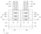
도 1a는 본 발명의 실시예들에 따른 반도체 장치를 설명하기 위한 평면도이다.
도 1b는 도 1a의 A-A'선에 따른 단면도이다.
도 1c는 도 1a의 B-B'선에 따른 단면도이다.
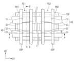
도 2a는 본 발명의 실시예들에 따른 반도체 장치를 설명하기 위한 평면도이다.
도 2b는 도 2a의 C-C'선에 따른 단면도이다.
도 2c는 도 2a의 D-D'선에 따른 단면도이다.
도 3a 내지 도 11a는 본 발명의 실시예들에 따른 반도체 장치의 제조 방법을 설명하기 위한 평면도들이다.
도 3b 내지 도 11b는 각각 도 3a 내지 도 11a의 A-A'선에 따른 단면도들이다.
도 3c 내지 도 11c는 각각 도 3a 내지 도 11a의 B-B'선에 따른 단면도들이다.FIG. 1a is a plan view illustrating a semiconductor device according to embodiments of the present invention.
Figure 1b is a cross-sectional view taken along line A-A' of Figure 1a.
Figure 1c is a cross-sectional view taken along line B-B' of Figure 1a.
FIG. 2a is a plan view illustrating a semiconductor device according to embodiments of the present invention.
Figure 2b is a cross-sectional view taken along line C-C' of Figure 2a.
Figure 2c is a cross-sectional view taken along line D-D' of Figure 2a.
FIGS. 3A to 11A are plan views illustrating a method for manufacturing a semiconductor device according to embodiments of the present invention.
Figures 3b to 11b are cross-sectional views taken along lines A-A' of Figures 3a to 11a, respectively.
Figures 3c to 11c are cross-sectional views taken along lines B-B' of Figures 3a to 11a, respectively.
도면들 참조하여 본 발명의 개념에 따른 반도체 장치를 설명한다.A semiconductor device according to the concept of the present invention is described with reference to the drawings.
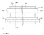
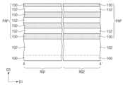
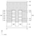
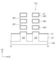
도 1a는 본 발명의 실시예들에 따른 반도체 장치를 설명하기 위한 평면도이다. 도 1b는 도 1a의 A-A'선에 따른 단면도이다. 도 1c는 도 1a의 B-B'선에 따른 단면도이다.FIG. 1A is a plan view for explaining a semiconductor device according to embodiments of the present invention. FIG. 1B is a cross-sectional view taken along line A-A' of FIG. 1A. FIG. 1C is a cross-sectional view taken along line B-B' of FIG. 1A.
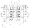
도 1a 내지 도 1c를 참조하여, 제 1 영역(RG1) 및 제 2 영역(RG2)을 포함하는 기판(100)이 제공될 수 있다. 기판(100)은 반도체 기판일 수 있다. 예를 들어, 기판(100)은 실리콘(Si) 기판 또는 게르마늄(Ge) 기판일 수 있다. 이와는 다르게, 기판(100)은 SOI(Silicon On Insulator) 기판일 수 있다. 기판(100)의 제 1 영역(RG1) 및 제 2 영역(RG2)은 제 1 방향(D1)으로 나란히 배치될 수 있다. 기판(100)의 제 1 영역(RG1) 및 제 2 영역(RG2)은 각각 제 1 트랜지스터들(TR1) 및 제 2 트랜지스터들(TR2)이 제공되는 영역으로 정의될 수 있다.Referring to FIGS. 1A to 1C, a substrate (100) including a first region (RG1) and a second region (RG2) may be provided. The substrate (100) may be a semiconductor substrate. For example, the substrate (100) may be a silicon (Si) substrate or a germanium (Ge) substrate. Alternatively, the substrate (100) may be a silicon on insulator (SOI) substrate. The first region (RG1) and the second region (RG2) of the substrate (100) may be arranged side by side in a first direction (D1). The first region (RG1) and the second region (RG2) of the substrate (100) may be defined as regions in which first transistors (TR1) and second transistors (TR2) are provided, respectively.
이하에서, 제 1 방향(D1) 및 제 2 방향(D2)은 기판(100)의 상면과 평행하고, 서로 수직한 방향으로 정의되고, 제 3 방향(D3)은 기판(100)의 상면과 수직한 방향으로 정의된다.Hereinafter, the first direction (D1) and the second direction (D2) are defined as directions parallel to the upper surface of the substrate (100) and perpendicular to each other, and the third direction (D3) is defined as a direction perpendicular to the upper surface of the substrate (100).
실시예들에 따르면, 기판(100)의 제 1 및 제 2 영역들(RG1, RG2)은, 데이터를 저장하기 위한 복수의 메모리 셀들이 형성되는 메모리 셀 영역일 수 있다. 예를 들어, 기판(100)의 메모리 셀 영역 상에, 복수의 에스램(SRAM) 셀들을 구성하는 메모리 셀 트랜지스터들이 배치될 수 있다. 제 1 및 제 2 트랜지스터들(RT1, TR2)은 상기 메모리 셀 트랜지스터들의 일부일 수 있다.According to embodiments, the first and second regions (RG1, RG2) of the substrate (100) may be memory cell regions in which a plurality of memory cells for storing data are formed. For example, memory cell transistors constituting a plurality of SRAM cells may be arranged on the memory cell region of the substrate (100). The first and second transistors (RT1, TR2) may be part of the memory cell transistors.
다른 실시예들에 따르면, 기판(100)의 제 1 및 제 2 영역들(RG1, RG2)은, 반도체 소자의 로직 회로를 구성하는 로직 트랜지스터들이 배치되는 로직 셀 영역일 수 있다. 예를 들어, 기판(100)의 로직 셀 영역 상에 로직 트랜지스터들이 배치될 수 있다. 제1 및 제 2 트랜지스터들(TR1, RT2)은 상기 로직 트랜지스터들의 일부일 수 있다. 그러나, 본 발명의 실시예들이 이에 제한되는 것은 아니다.According to other embodiments, the first and second regions (RG1, RG2) of the substrate (100) may be logic cell regions in which logic transistors constituting a logic circuit of a semiconductor device are arranged. For example, logic transistors may be arranged on the logic cell region of the substrate (100). The first and second transistors (TR1, RT2) may be part of the logic transistors. However, embodiments of the present invention are not limited thereto.
제 1 및 제 2 영역들(RG1, RG2) 상의 제 1 및 제 2 트랜지스터들(TR1, TR2)의 도전형은 서로 동일할 수 있다. 예를 들어, 제 1 및 제 2 영역들(RG1, RG2) 상의 제 1 및 제 2 트랜지스터들(TR1, TR2)은 NMOSFET일 수 있다. 또는, 제 1 및 제 2 영역들(RG1, RG2) 상의 제 1 및 제 2 트랜지스터들(TR1, TR2)은 PMOSFET일 수 있다. 이와는 다르게, 제 1 및 제 2 트랜지스터들(TR1, TR2)의 도전형은 서로 다를 수 있다. 예를 들어, 제 1 영역들(RG1) 상의 제 1 트랜지스터들(TR1)은 NMOSFET이고, 제 2 영역들(RG2) 상의 제 2 트랜지스터들(TR2)은 PMOSFET일 수 있다.The conductivity types of the first and second transistors (TR1, TR2) on the first and second regions (RG1, RG2) may be the same. For example, the first and second transistors (TR1, TR2) on the first and second regions (RG1, RG2) may be NMOSFETs. Alternatively, the first and second transistors (TR1, TR2) on the first and second regions (RG1, RG2) may be PMOSFETs. Alternatively, the conductivity types of the first and second transistors (TR1, TR2) may be different. For example, the first transistors (TR1) on the first regions (RG1) may be NMOSFETs and the second transistors (TR2) on the second regions (RG2) may be PMOSFETs.
기판(100) 상에 기저 활성 패턴(base active pattern, 102)이 제공될 수 있다. 기저 활성 패턴(102)은 기판(100)으로부터 제 3 방향(D3)으로 돌출될 수 있다. 기저 활성 패턴(102)은 제 1 방향(D1)으로 연장될 수 있다. 기저 활성 패턴(102)은, 도 1a 및 도 1c에 도시된 바와 같이, 복수로 제공될 수 있고, 복수의 기저 활성 패턴들(102)은 제 2 방향(D2)으로 배열될 수 있다.A base active pattern (102) may be provided on a substrate (100). The base active pattern (102) may protrude from the substrate (100) in a third direction (D3). The base active pattern (102) may extend in a first direction (D1). The base active pattern (102) may be provided in multiple numbers, as shown in FIGS. 1A and 1C, and the multiple base active patterns (102) may be arranged in the second direction (D2).
기저 활성 패턴들(102) 각각의 양측으로 소자 분리막(ST)이 기판(100) 상에 제공될 수 있다. 소자 분리막(ST)은 제 1 방향(D1)으로 연장될 수 있다. 소자 분리막(ST)은 기저 활성 패턴들(102) 사이의 공간을 채울 수 있다. 소자 분리막(ST)은 기저 활성 패턴들(102)의 상부 측벽들을 노출할 수 있다. 예를 들어, 소자 분리막(ST)의 상면은 기저 활성 패턴들(102)의 상면보다 낮은 레벨에 있을 수 있다. 소자 분리막(ST)은 산화물, 질화물 또는 산질화물을 포함할 수 있다.A device isolation film (ST) may be provided on the substrate (100) on both sides of each of the base active patterns (102). The device isolation film (ST) may extend in the first direction (D1). The device isolation film (ST) may fill a space between the base active patterns (102). The device isolation film (ST) may expose upper sidewalls of the base active patterns (102). For example, an upper surface of the device isolation film (ST) may be at a lower level than an upper surface of the base active patterns (102). The device isolation film (ST) may include an oxide, a nitride, or an oxynitride.
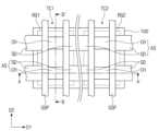
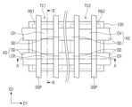
기저 활성 패턴들(102) 상에 활성 구조체들(AS)이 제공될 수 있다. 활성 구조체들(AS)은 평면적 관점에서, 기저 활성 패턴들(102)과 중첩하도록 제공될 수 있다. 활성 구조체들(AS)은 제 1 방향(D1)을 따라 연장되는 라인 형태를 가질 수 있다. 예를 들어, 활성 구조체들(AS)은 기저 활성 패턴들(102)의 상면을 따라 제 1 방향(D1)으로 연장될 수 있다.Active structures (AS) may be provided on the base active patterns (102). The active structures (AS) may be provided so as to overlap the base active patterns (102) in a planar view. The active structures (AS) may have a line shape extending along the first direction (D1). For example, the active structures (AS) may extend along the upper surface of the base active patterns (102) in the first direction (D1).
각각의 활성 구조체들(AS)은, 채널 패턴(CH) 및 소스/드레인 패턴들(SD)을 포함할 수 있다. 채널 패턴(CH)은 한 쌍의 소스/드레인 패턴들(SD) 사이에 개재될 수 있다. 채널 패턴(CH) 및 소스/드레인 패턴들(SD)은 기저 활성 패턴(102)의 상면을 따라 제 1 방향(D1)으로 배열될 수 있다. 제 1 영역(RG1)의 채널 패턴(CH)은 수직적으로 적층된 복수의 제 1 반도체 패턴들(NS1)을 포함할 수 있다. 제 2 영역(RG2)의 채널 패턴(CH)은 수직적으로 적층된 복수의 제 2 반도체 패턴들(NS2)을 포함할 수 있다.Each of the active structures (AS) may include a channel pattern (CH) and source/drain patterns (SD). The channel pattern (CH) may be interposed between a pair of source/drain patterns (SD). The channel pattern (CH) and the source/drain patterns (SD) may be arranged in a first direction (D1) along a top surface of the base active pattern (102). The channel pattern (CH) of the first region (RG1) may include a plurality of first semiconductor patterns (NS1) that are vertically stacked. The channel pattern (CH) of the second region (RG2) may include a plurality of second semiconductor patterns (NS2) that are vertically stacked.
제 1 반도체 패턴들(NS1)은 제 3 방향(D3)으로 서로 이격될 수 있다. 제 1 반도체 패턴들(NS1) 중 최하단의 제 1 반도체 패턴(NS1)은 제 3 방향(D3)으로 기저 활성 패턴(102)으로부터 이격될 수 있다. 제 1 반도체 패턴들(NS1)이 제 3 방향(D3)으로 이격된 거리는 1nm 내지 15nm일 수 있다. 각각의 소스/드레인 패턴들(SD)은 제 1 반도체 패턴들(NS1)의 측벽들과 직접 접촉할 수 있다. 즉, 제 1 반도체 패턴들(NS1)은, 인접하는 한 쌍의 소스/드레인 패턴들(SD)을 서로 연결할 수 있다. 도 1b 및 1c에서 제 1 영역(RG1)의 채널 패턴(CH)의 제 1 반도체 패턴들(NS1)이 3개인 것을 도시하였으나, 본 발명에서 이들의 개수는 특별히 제한되지 않는다. 제 1 반도체 패턴들(NS1)은 서로 동일한 두께를 갖거나, 또는 서로 다른 두께를 가질 수 있다. 제 1 반도체 패턴들(NS1)은 실리콘(Si), 실리콘 게르마늄(SiGe) 또는 게르마늄(Ge) 중 적어도 하나를 포함할 수 있다. 제 1 반도체 패턴들(NS1)은 필요에 따라 불순물이 도핑될 수 있다. 예를 들어, 제 1 트랜지스터들(TR1)이 NMOFET인 경우, 상기 불순물은 보론(B)일 수 있다. 제 1 트랜지스터들(TR1)이 PMOSFET인 경우, 상기 불순물은 인(P)일 수 있다.The first semiconductor patterns (NS1) may be spaced apart from each other in a third direction (D3). The lowermost first semiconductor pattern (NS1) among the first semiconductor patterns (NS1) may be spaced apart from the base active pattern (102) in the third direction (D3). The distance at which the first semiconductor patterns (NS1) are spaced apart in the third direction (D3) may be 1 nm to 15 nm. Each of the source/drain patterns (SD) may be in direct contact with the sidewalls of the first semiconductor patterns (NS1). That is, the first semiconductor patterns (NS1) may connect a pair of adjacent source/drain patterns (SD) to each other. Although the number of first semiconductor patterns (NS1) of the channel pattern (CH) of the first region (RG1) is illustrated as three in FIGS. 1B and 1C , the number thereof is not particularly limited in the present invention. The first semiconductor patterns (NS1) may have the same thickness or different thicknesses. The first semiconductor patterns (NS1) may include at least one of silicon (Si), silicon germanium (SiGe), or germanium (Ge). The first semiconductor patterns (NS1) may be doped with an impurity as needed. For example, when the first transistors (TR1) are NMOFETs, the impurity may be boron (B). When the first transistors (TR1) are PMOSFETs, the impurity may be phosphorus (P).
제 2 반도체 패턴들(NS2)에 대한 구체적인 설명은, 상기한 제 1 반도체 패턴들(NS1)에 대한 설명과 동일할 수 있다. 제 1 및 제 2 트랜지스터들(TR1, TR2)이 서로 다른 도전형을 가질 경우, 제 2 반도체 패턴들(NS2)은 제 1 반도체 패턴들(NS1)과는 다른 불순물이 도핑될 수 있다.A specific description of the second semiconductor patterns (NS2) may be the same as the description of the first semiconductor patterns (NS1) described above. When the first and second transistors (TR1, TR2) have different conductivity types, the second semiconductor patterns (NS2) may be doped with impurities different from those of the first semiconductor patterns (NS1).
동일한 레벨에 위치하는 제 1 및 제 2 반도체 패턴들(NS1, NS2)은 동일한 반도체층으로부터 형성된 것일 수 있다. 동일한 레벨에 위치하는 제 1 및 제 2 반도체 패턴들(NS1, NS2)은 서로 실질적으로 동일한 두께를 가질 수 있다. 동일한 레벨에 위치하는 제 1 및 제 2 반도체 패턴들(NS1, NS2)은 서로 실질적으로 동일한 반도체 물질을 포함할 수 있다.The first and second semiconductor patterns (NS1, NS2) positioned at the same level may be formed from the same semiconductor layer. The first and second semiconductor patterns (NS1, NS2) positioned at the same level may have substantially the same thickness. The first and second semiconductor patterns (NS1, NS2) positioned at the same level may include substantially the same semiconductor material.
소스/드레인 패턴들(SD)은 제 1 및 제 2 반도체 패턴들(NS1, NS2) 및 기저 활성 패턴들(102)을 시드로 이용하여 형성된 에피팩시얼(epitaxial) 패턴들일 수 있다. 예를 들어, 제 1 및 제 2 트랜지스터들(TR1, TR2)이 NMOSFET인 경우, 소스/드레인 패턴들(SD)은 채널 패턴(CH)에 인장성 스트레인을 제공하는 반도체 물질을 포함할 수 있다. 일 예로, 소스/드레인 패턴들(SD)은 채널 패턴(CH)의 반도체 원소의 격자 상수보다 작은 격자 상수를 갖는 반도체 원소를 포함할 수 있다. 이와는 다르게, 소스/드레인 패턴들(SD)은 채널 패턴(CH)의 반도체 원소와 동일한 반도체 원소를 포함할 수 있다. 또는, 제 1 및 제 2 트랜지스터들(TR1, TR2)이 PMOSFET인 경우, 소스/드레인 패턴들(SD)은 채널 패턴(CH)에 압축성 스트레인을 제공하는 물질을 포함할 수 있다. 일 예로, 소스/드레인 패턴들(SD)은 채널 패턴(CH)의 반도체 원소의 격자 상수보다 큰 격자 상수를 갖는 반도체 원소를 포함할 수 있다.The source/drain patterns (SD) may be epitaxial patterns formed using the first and second semiconductor patterns (NS1, NS2) and the base active patterns (102) as seeds. For example, when the first and second transistors (TR1, TR2) are NMOSFETs, the source/drain patterns (SD) may include a semiconductor material that provides a tensile strain to the channel pattern (CH). For example, the source/drain patterns (SD) may include a semiconductor element having a lattice constant smaller than a lattice constant of a semiconductor element of the channel pattern (CH). Alternatively, the source/drain patterns (SD) may include the same semiconductor element as the semiconductor element of the channel pattern (CH). Alternatively, when the first and second transistors (TR1, TR2) are PMOSFETs, the source/drain patterns (SD) may include a material that provides a compressive strain to the channel pattern (CH). For example, the source/drain patterns (SD) may include a semiconductor element having a lattice constant greater than a lattice constant of a semiconductor element of the channel pattern (CH).
소스/드레인 패턴들(SD)은 불순물을 더 포함할 수 있다. 상기 불순물은 소스/드레인 패턴들(SD)을 포함하는 제 1 및 제 2 트랜지스터들(TR1, TR2)의 전기적 특성을 개선하기 위하여 채용될 수 있다. 제 1 및 제 2 트랜지스터들(TR1, TR2)이 NMOFET인 경우, 상기 불순물은 인(P)일 수 있다. 제 1 및 제 2 트랜지스터들(TR1, TR2)이 PMOSFET인 경우, 상기 불순물은 보론(B)일 수 있다.The source/drain patterns (SD) may further include impurities. The impurities may be employed to improve electrical characteristics of the first and second transistors (TR1, TR2) including the source/drain patterns (SD). When the first and second transistors (TR1, TR2) are NMOFETs, the impurities may be phosphorus (P). When the first and second transistors (TR1, TR2) are PMOSFETs, the impurities may be boron (B).
활성 구조체들(AS) 상에 제 1 및 제 2 게이트 구조체들(GS1, GS2)이 제공될 수 있다. 제 1 및 제 2 게이트 구조체들(GS1, GS2)은 제 1 및 제 2 영역들(RG1, RG2)의 채널 패턴들(CH)을 각각 가로지르며, 제 2 방향(D2)으로 연장될 수 있다. 제 1 및 제 2 게이트 구조체들(GS1, GS2)은 제 1 방향(D1)으로 서로 이격될 수 있다. 평면적 관점에서, 제 1 영역(RG1)의 채널 패턴들(CH)은 제 1 게이트 구조체(GS1)와 중첩할 수 있고, 제 2 영역(RG2)의 채널 패턴들(CH)은 제 2 게이트 구조체(GS2)와 중첩할 수 있다. 소스/드레인 패턴들(SD)은 제 1 게이트 구조체(GS1)의 양측 및 제 2 게이트 구조체(GS2)의 양측에 제공될 수 있다.First and second gate structures (GS1, GS2) may be provided on active structures (AS). The first and second gate structures (GS1, GS2) may extend in a second direction (D2) while crossing channel patterns (CH) of the first and second regions (RG1, RG2), respectively. The first and second gate structures (GS1, GS2) may be spaced apart from each other in the first direction (D1). In a planar view, the channel patterns (CH) of the first region (RG1) may overlap the first gate structure (GS1), and the channel patterns (CH) of the second region (RG2) may overlap the second gate structure (GS2). Source/drain patterns (SD) can be provided on both sides of the first gate structure (GS1) and on both sides of the second gate structure (GS2).
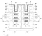
제 1 및 제 2 게이트 구조체들(GS1, GS2)은 제 1 및 제 2 일함수 조절 패턴들(WF1, WF2)을 포함할 수 있다. 제 1 및 제 2 게이트 구조체들(GS1, GS2)은 게이트 전극들(GE)을 포함할 수 있다.The first and second gate structures (GS1, GS2) may include first and second work function control patterns (WF1, WF2). The first and second gate structures (GS1, GS2) may include gate electrodes (GE).
각각의 제 1 및 제 2 게이트 구조체들(GS1, GS2)은 제 1 부분(P1) 및 제 2 부분(P2)을 가질 수 있다. 제 1 부분(P1)은 서로 수직하게 인접하는 반도체 패턴들(NS1, NS2) 사이의 공간에 위치할 수 있다. 즉, 제 1 부분(P1)은 서로 수직하게 인접하는 반도체 패턴들(NS1, NS2) 사이에 개재되는 부분일 수 있다. 제 2 부분(P2)은 최상부의 반도체 패턴(NS1, NS2) 상의 공간에 위치할 수 있다. 상기 최상부의 반도체 패턴(NS1, NS2) 상의 공간은 후술할 한 쌍의 게이트 스페이서들(GSP) 및 최상부의 반도체 패턴(NS1, NS2)에 의해 둘러싸인 공간일 수 있다. 즉, 제 2 부분(P2)은 최상부의 반도체 패턴(NS1, NS2) 상에 위치하며, 한 쌍의 게이트 스페이서들(GSP) 사이에 개재된 부분일 수 있다.Each of the first and second gate structures (GS1, GS2) may have a first portion (P1) and a second portion (P2). The first portion (P1) may be located in a space between vertically adjacent semiconductor patterns (NS1, NS2). That is, the first portion (P1) may be a portion interposed between vertically adjacent semiconductor patterns (NS1, NS2). The second portion (P2) may be located in a space on the uppermost semiconductor pattern (NS1, NS2). The space on the uppermost semiconductor pattern (NS1, NS2) may be a space surrounded by a pair of gate spacers (GSP) and the uppermost semiconductor pattern (NS1, NS2) to be described later. That is, the second portion (P2) may be a portion interposed between a pair of gate spacers (GSP) and the uppermost semiconductor pattern (NS1, NS2) located on the uppermost semiconductor pattern (NS1, NS2).
제 1 부분(P1)에서, 제 1 일함수 조절 패턴들(WF1)은 각각 제 1 반도체 패턴들(NS1)의 표면을 덮을 수 있다. 예를 들어, 도 1c에 도시된 바와 같이, 제 1 일함수 조절 패턴들(WF1)은 제 1 반도체 패턴들(NS1)의 외주면을 둘러싸거나, 제 2 반도체 패턴들(NS2)의 외주면을 둘러쌀 수 있다. 여기서 반도체 패턴들(NS1, NS2)의 외주면이라하면, 제 2 방향(D2)으로 노출되는 반도체 패턴들(SN1, NS2)의 측면들 및 제 3 방향(D3)으로 노출되는 반도체 패턴들(NS1, NS2)의 상면 및 하면을 말한다. 즉, 각각의 제 1 및 제 2 트랜지스터들(TR1, TR2)은 게이트-올-어라운드(gate-all-around)형 전계 효과 트랜지스터일 수 있다. 제 1 일함수 조절 패턴(WF1)은 상대적으로 일함수가 낮은 금속 화합물을 포함할 수 있다. 일 예로, 제 1 일함수 조절 패턴(WF1)은 알루미늄(Al)이 도핑(또는 함유된) 금속 화합물일 수 있다. 바람직하게는, 제 1 일함수 조절 패턴(WF1)은 티타늄 알루미늄 탄화물(TiAlC), 티타늄 알루미늄 질화물(TiAlN) 또는 탄탈 알루미늄 질화물(TaAlN)을 포함할 수 있다. 이때, 제 1 일함수 조절 패턴(WF1) 내의 산소(O) 함유량은 0% 내지 30%일 수 있다.In the first portion (P1), the first work function control patterns (WF1) may cover the surfaces of the first semiconductor patterns (NS1), respectively. For example, as illustrated in FIG. 1C, the first work function control patterns (WF1) may surround the outer peripheral surfaces of the first semiconductor patterns (NS1) or the outer peripheral surfaces of the second semiconductor patterns (NS2). Here, the outer peripheral surfaces of the semiconductor patterns (NS1, NS2) refer to the side surfaces of the semiconductor patterns (SN1, NS2) exposed in the second direction (D2) and the upper and lower surfaces of the semiconductor patterns (NS1, NS2) exposed in the third direction (D3). That is, each of the first and second transistors (TR1, TR2) may be a gate-all-around type field effect transistor. The first work function control pattern (WF1) may include a metal compound having a relatively low work function. For example, the first work function control pattern (WF1) may be a metal compound doped with (or containing) aluminum (Al). Preferably, the first work function control pattern (WF1) may include titanium aluminum carbide (TiAlC), titanium aluminum nitride (TiAlN), or tantalum aluminum nitride (TaAlN). In this case, the oxygen (O) content in the first work function control pattern (WF1) may be 0% to 30%.
제 1 부분(P1)에서, 제 1 일함수 조절 패턴들(WF1)과 제 2 일함수 조절 패턴들(WF2)은 반도체 패턴들(NS1, NS2)의 표면 상에 순차적으로 적층될 수 있다. 예를 들어, 도 1c에 도시된 바와 같이, 제 1 일함수 조절 패턴들(WF1)은 반도체 패턴들(NS1, NS2)의 외주면을 둘러쌀 수 있고, 제 2 일함수 조절 패턴들(WF2)은 제 1 일함수 조절 패턴들(WF1)의 외주면들을 둘러쌀 수 있다. 제 2 일함수 조절 패턴들(WF2)은 제 1 일함수 조절 패턴들(WF1)과 직접적으로 접할 수 있다. 예를 들어, 서로 적층되는 제 1 일함수 조절 패턴(WF1)과 제 2 일함수 조절 패턴(WF2) 사이에 산화물층 또는 질화물층과 같은 물질층이 개재되지 않을 수 있다. 제 2 일함수 조절 패턴(WF2)은 상대적으로 일함수가 높은 금속 화합물을 포함할 수 있다. 일 예로, 제 2 일함수 조절 패턴(WF2)은 티타늄 질화물(TiN), 티타늄 산질화물(TiON) 또는 탄탈 질화물(TaN)을 포함할 수 있다. 다른 실시예들에 따르면, 제 2 일함수 조절 패턴(WF2)은 티타늄 산질화물(TiON)과 티타늄 질화물(TiN)의 다층 구조체를 포함할 수 있다. 제 2 일함수 조절 패턴(WF2)이 티타늄 산질화물(TiON)을 포함하는 경우, 제 2 일함수 조절 패턴(WF2) 내의 산소(O) 함유량은 30% 내지 60%일 수 있다.In the first portion (P1), the first work function control patterns (WF1) and the second work function control patterns (WF2) may be sequentially stacked on the surfaces of the semiconductor patterns (NS1, NS2). For example, as illustrated in FIG. 1C, the first work function control patterns (WF1) may surround outer surfaces of the semiconductor patterns (NS1, NS2), and the second work function control patterns (WF2) may surround outer surfaces of the first work function control patterns (WF1). The second work function control patterns (WF2) may be in direct contact with the first work function control patterns (WF1). For example, a material layer such as an oxide layer or a nitride layer may not be interposed between the first work function control pattern (WF1) and the second work function control pattern (WF2) that are stacked on each other. The second work function control pattern (WF2) may include a metal compound having a relatively high work function. For example, the second work function control pattern (WF2) may include titanium nitride (TiN), titanium oxynitride (TiON), or tantalum nitride (TaN). According to other embodiments, the second work function control pattern (WF2) may include a multilayer structure of titanium oxynitride (TiON) and titanium nitride (TiN). When the second work function control pattern (WF2) includes titanium oxynitride (TiON), the oxygen (O) content in the second work function control pattern (WF2) may be 30% to 60%.
제 1 및 제 2 게이트 구조체들(GS1, GS2)의 제 2 부분(P2)은 순차적으로 적층된 제 1 일함수 조절 패턴(WF1) 및 제 2 일함수 조절 패턴(WF2)으로 이루어질 수 있다.The second part (P2) of the first and second gate structures (GS1, GS2) may be composed of a first work function control pattern (WF1) and a second work function control pattern (WF2) that are sequentially stacked.
게이트 전극들(GE)은 제 1 부분(P1)에서, 제 1 반도체 패턴들(NS1) 사이의 공간 및 제 2 반도체 패턴들(NS2) 사이의 공간을 채울 수 있다. 더하여, 게이트 전극들(GE)은 제 2 부분(P2)에서, 제 1 및 제 2 일함수 조절 패턴들(WF1, WF2) 상에 배치될 수 있다. 게이트 전극들(GE)은 제 1 및 제 2 일함수 조절 패턴들(WF1, WF2)에 비해 저항이 낮을 수 있다. 예를 들어, 게이트 전극들(GE)은 알루미늄(Al), 텅스텐(W), 티타늄(Ti) 또는 탄탈륨(Ta)과 같은 저저항 금속을 포함할 수 있다.The gate electrodes (GE) can fill a space between the first semiconductor patterns (NS1) and a space between the second semiconductor patterns (NS2) in the first portion (P1). In addition, the gate electrodes (GE) can be arranged on the first and second work function control patterns (WF1, WF2) in the second portion (P2). The gate electrodes (GE) can have lower resistance than the first and second work function control patterns (WF1, WF2). For example, the gate electrodes (GE) can include a low-resistance metal such as aluminum (Al), tungsten (W), titanium (Ti), or tantalum (Ta).
제 1 및 제 2 게이트 구조체들(GS1, GS2) 각각의 양 측벽들 상에 한 쌍의 게이트 스페이서들(GSP)이 배치될 수 있다. 게이트 스페이서들(GSP)은 제 1 및 제 2 게이트 구조체들(GS1, GS2)을 따라 제 2 방향(D2)으로 연장될 수 있다. 게이트 스페이서들(GSP)의 상면은 제 1 및 제 2 게이트 구조체들(GS1, GS2)의 상면들보다 높을 수 있다. 채널 패턴들(CH) 상(즉, 제 2 부분(P2))의 제 1 및 제 2 일함수 조절 패턴들(WF1, WF2)은 게이트 스페이서들(GSP)의 내측벽들을 따라 제 3 방향(D3)으로 연장될 수 있다. 게이트 스페이서들(GSP)은 실리콘 탄질화물(SiCN), 실리콘 탄소 산질화물(SiCON), 실리콘 질화물(SiN) 또는 이들의 다중 막(multi-layer)를 포함할 수 있다.A pair of gate spacers (GSP) may be arranged on each of the sidewalls of the first and second gate structures (GS1, GS2). The gate spacers (GSP) may extend in a second direction (D2) along the first and second gate structures (GS1, GS2). Top surfaces of the gate spacers (GSP) may be higher than top surfaces of the first and second gate structures (GS1, GS2). The first and second work function control patterns (WF1, WF2) on the channel patterns (CH) (i.e., the second portion (P2)) may extend in a third direction (D3) along the inner sidewalls of the gate spacers (GSP). Gate spacers (GSPs) may include silicon carbon nitride (SiCN), silicon carbon oxynitride (SiCON), silicon nitride (SiN), or multi-layers thereof.
제 1 및 제 2 게이트 구조체들(GS1, GS2) 상에 게이트 캐핑 패턴들(CP)이 제공될 수 있다. 게이트 캐핑 패턴들(CP)은 제 1 및 제 2 게이트 구조체들(GS1, GS2)을 따라 제 2 방향(D2)으로 연장될 수 있다. 게이트 캐핑 패턴들(CP)의 상면들은 게이트 스페이서들(GSP)의 상면들과 공면을 이룰 수 있다. 게이트 캐핑 패턴들(CP)은 실리콘 산질화물(SiON), 실리콘 탄질화물(SiCN) 또는 실리콘 질화물(SiN)을 포함할 수 있다.Gate capping patterns (CP) may be provided on the first and second gate structures (GS1, GS2). The gate capping patterns (CP) may extend in a second direction (D2) along the first and second gate structures (GS1, GS2). Top surfaces of the gate capping patterns (CP) may be coplanar with top surfaces of the gate spacers (GSP). The gate capping patterns (CP) may include silicon oxynitride (SiON), silicon carbonitride (SiCN), or silicon nitride (SiN).
스페이서 패턴들(110)이 소스/드레인 패턴들(SD)의 각각과 제 1 및 제 2 게이트 구조체들(GS1, GS2) 사이에 제공될 수 있다. 스페이서 패턴들(110)은 제 1 및 제 2 게이트 구조체들(GS1, GS2) 각각의 일측에 제공될 수 있고, 제 3 방향(D3)을 따라 서로 이격될 수 있다. 즉, 스페이서 패턴들(110) 및 반도체 패턴들(NS1, NS2)은 제 3 방향(D3)을 따라 교대로 그리고 반복적으로 적층될 수 있다. 스페이서 패턴들(110)의 각각은 서로 인접하는 반도체 패턴들(NS1, NS2) 사이, 또는 최하층의 반도체 패턴(NS1, NS2)과 기저 활성 패턴(102) 사이에 제공될 수 있다. 소스/드레인 패턴들(SD)의 각각은 반도체 패턴들(NS1, NS2)과 접할 수 있고, 스페이서 패턴들(110)을 사이에 두고 제 1 및 제 2 게이트 구조체들(GS1, GS2)로부터 이격될 수 있다. 스페이서 패턴들(110)은 제 1 및 제 2 게이트 구조체들(GS1, GS2)을 소스/드레인 패턴들(SD)로부터 전기적으로 절연시킬 수 있다. 스페이서 패턴들(110)은 실리콘 질화물(SiN)을 포함할 수 있다.Spacer patterns (110) may be provided between each of the source/drain patterns (SD) and the first and second gate structures (GS1, GS2). The spacer patterns (110) may be provided on one side of each of the first and second gate structures (GS1, GS2) and may be spaced apart from each other along the third direction (D3). That is, the spacer patterns (110) and the semiconductor patterns (NS1, NS2) may be alternately and repeatedly stacked along the third direction (D3). Each of the spacer patterns (110) may be provided between adjacent semiconductor patterns (NS1, NS2), or between the lowermost semiconductor pattern (NS1, NS2) and the base active pattern (102). Each of the source/drain patterns (SD) may be in contact with the semiconductor patterns (NS1, NS2) and may be spaced apart from the first and second gate structures (GS1, GS2) with spacer patterns (110) therebetween. The spacer patterns (110) may electrically insulate the first and second gate structures (GS1, GS2) from the source/drain patterns (SD). The spacer patterns (110) may include silicon nitride (SiN).
제 1 및 제 2 반도체 패턴들(NS1, NS2)과 제 1 및 제 2 게이트 구조체들(GS1, GS2) 사이에 게이트 유전막들(GI)이 개재될 수 있다. 각각의 게이트 유전막들(GI)은 제 1 반도체 패턴들(NS1) 사이의 공간 및 제 2 반도체 패턴들(NS2) 사이의 공간을 부분적으로 컨포멀하게 채울 수 있다. 게이트 유전막들(GI)은 실리콘 산화막보다 유전상수가 높은 고유전율 물질을 포함할 수 있다. 일 예로, 상기 고유전율 물질은 하프늄 산화물(HfO), 하프늄 실리콘 산화물(HfSiO), 란탄 산화물(LAO), 지르코늄 산화물(ZrO), 지르코늄 실리콘 산화물(ZrSiO), 탄탈 산화물(TaO), 티타늄 산화물(TiO), 바륨 스트론튬 티타늄 산화물(BaSrTiO), 바륨 티타늄 산화물(BaTiO), 스트론튬 티타늄 산화물(SrTiO), 리튬 산화물(LiO), 알루미늄 산화물(Al2O3), 납 스칸듐 탄탈 산화물(PbScTaO), 및 납 아연 니오브산염(PbZnNbO) 중 적어도 하나를 포함할 수 있다.Gate dielectric films (GI) may be interposed between the first and second semiconductor patterns (NS1, NS2) and the first and second gate structures (GS1, GS2). Each of the gate dielectric films (GI) may partially conformally fill a space between the first semiconductor patterns (NS1) and a space between the second semiconductor patterns (NS2). The gate dielectric films (GI) may include a high-k material having a higher dielectric constant than a silicon oxide film. For example, the high-k material may include at least one of hafnium oxide (HfO), hafnium silicon oxide (HfSiO), lanthanum oxide (LAO), zirconium oxide (ZrO), zirconium silicon oxide (ZrSiO), tantalum oxide (TaO), titanium oxide (TiO), barium strontium titanium oxide (BaSrTiO), barium titanium oxide (BaTiO), strontium titanium oxide (SrTiO), lithium oxide (LiO), aluminum oxide (Al2 O3 ), lead scandium tantalum oxide (PbScTaO), and lead zinc niobate (PbZnNbO).
여기서, 인접한 제 1 및 제 2 반도체 패턴들(NS1, NS2)을 둘러싸는 게이트 유전막들(GI) 사이의 간격은 10nm보다 작을 수 있다. 즉, 인접한 제 1 및 제 2 반도체 패턴들(NS1, NS2) 사이에서 제 1 및 제 2 일함수 조절 패턴들(WF1, WF2) 및 게이트 전극들(GE)이 채워지는 공간의 높이는 10nm보다 작을 수 있다.Here, the gap between the gate dielectric films (GI) surrounding the adjacent first and second semiconductor patterns (NS1, NS2) can be smaller than 10 nm. That is, the height of the space filled with the first and second work function control patterns (WF1, WF2) and the gate electrodes (GE) between the adjacent first and second semiconductor patterns (NS1, NS2) can be smaller than 10 nm.
제 1 및 제 2 트랜지스터들(TR1, TR2)에 있어서, 제 1 트랜지스터(TR1)의 문턱 전압은 제 2 트랜지스터(TR2)의 문턱 전압보다 낮을 수 있다. 예를 들어, 제 1 트랜지스터(TR1)의 제 1 일함수 조절 패턴(WF1)과 제 2 트랜지스터(TR2)의 제 1 일함수 조절 패턴(WF1)은 서로 다른 물질을 포함할 수 있다.In the first and second transistors (TR1, TR2), the threshold voltage of the first transistor (TR1) may be lower than the threshold voltage of the second transistor (TR2). For example, the first work function control pattern (WF1) of the first transistor (TR1) and the first work function control pattern (WF1) of the second transistor (TR2) may include different materials.
제 1 트랜지스터(TR1)의 제 1 일함수 조절 패턴(WF1)은 상대적으로 일함수가 낮은 금속 화합물을 포함할 수 있다. 일 예로, 제 1 트랜지스터(TR1)의 제 1 일함수 조절 패턴(WF1)은 알루미늄(Al)이 도핑(또는 함유된) 금속 화합물일 수 있다. 바람직하게는, 제 1 트랜지스터(TR1)의 제 1 일함수 조절 패턴(WF1)은 티타늄 알루미늄 탄화물(TiAlC), 티타늄 알루미늄 질화물(TiAlN) 또는 탄탈 알루미늄 질화물(TaAlN)을 포함할 수 있다. 제 1 트랜지스터(TR1)의 제 1 일함수 조절 패턴(WF1)에 있어서, 도펀트인 알루미늄(Al)의 도핑 농도를 조절하여 제 1 트랜지스터(TR1)의 제 1 일함수 조절 패턴(WF1)의 일함수를 조절할 수 있다.The first work function control pattern (WF1) of the first transistor (TR1) may include a metal compound having a relatively low work function. For example, the first work function control pattern (WF1) of the first transistor (TR1) may be a metal compound doped with (or containing) aluminum (Al). Preferably, the first work function control pattern (WF1) of the first transistor (TR1) may include titanium aluminum carbide (TiAlC), titanium aluminum nitride (TiAlN), or tantalum aluminum nitride (TaAlN). In the first work function control pattern (WF1) of the first transistor (TR1), the work function of the first work function control pattern (WF1) of the first transistor (TR1) may be controlled by controlling the doping concentration of aluminum (Al), which is a dopant.
제 2 트랜지스터(TR2)의 제 1 일함수 조절 패턴(WF1)은 제 1 트랜지스터(TR1)의 제 1 일함수 조절 패턴(WF1)에 비해 일함수가 높은 금속 화합물을 포함할 수 있다. 일 예로, 제 2 트랜지스터(TR2)의 제 1 일함수 조절 패턴(WF1)은 티타늄 질화물(TiN), 티타늄 산질화물(TiON) 또는 탄탈 질화물(TaN)을 포함할 수 있다. 제 2 트랜지스터(TR2)의 제 1 일함수 조절 패턴(WF1)은 불순물(일 예로, 알루미늄(Al) 등)을 실질적으로 함유하지 않을 수 있다.The first work function control pattern (WF1) of the second transistor (TR2) may include a metal compound having a higher work function than the first work function control pattern (WF1) of the first transistor (TR1). For example, the first work function control pattern (WF1) of the second transistor (TR2) may include titanium nitride (TiN), titanium oxynitride (TiON), or tantalum nitride (TaN). The first work function control pattern (WF1) of the second transistor (TR2) may substantially not contain an impurity (for example, aluminum (Al), etc.).
실시예들에서, 제 1 트랜지스터(TR1)과 제 2 트랜지스터(TR2)는 다른 도전형의 트랜지스터일 수 있다. 예를 들어, 제 1 트랜지스터들(TR1)은 NMOSFET이고, 제 2 트랜지스터들(TR2)은 PMOSFET일 수 있다. 이때, 제 1 트랜지스터(TR1)의 제 1 일함수 조절 패턴(WF1)은 낮은 일함수의 물질(일 예로, 티타늄 알루미늄 탄화물(TiAlC) 등)을 포함하고, 제 2 트랜지스터(TR2)의 제 1 일함수 조절 패턴(WF1)은 높은 일함수의 물질(일 예로, 티타늄 산질화물(TiON) 또는 티타늄 산질화물(TiON)과 티타늄 질화물(TiN)의 다층 구조체 등)을 포함할 수 있다. 그러나, 본 발명이 이에 한정되는 것은 아니며, 제 1 및 제 2 트랜지스터들(TR1, TR2)은 다른 문턱전압을 갖는 동일한 도전형의 트랜지스터로 구성될 수 있다.In the embodiments, the first transistor (TR1) and the second transistor (TR2) may be transistors of different conductivity types. For example, the first transistors (TR1) may be NMOSFETs, and the second transistors (TR2) may be PMOSFETs. At this time, the first work function control pattern (WF1) of the first transistor (TR1) may include a low work function material (for example, titanium aluminum carbide (TiAlC) or the like), and the first work function control pattern (WF1) of the second transistor (TR2) may include a high work function material (for example, titanium oxynitride (TiON) or a multilayer structure of titanium oxynitride (TiON) and titanium nitride (TiN) or the like). However, the present invention is not limited thereto, and the first and second transistors (TR1, TR2) may be configured as transistors of the same conductivity type having different threshold voltages.
본 발명에 따르면, 서로 적층되는 제 1 일함수 조절 패턴(WF1)과 제 2 일함수 조절 패턴(WF2) 사이에 산화물층 또는 질화물층과 같은 물질층이 개재되지 않을 수 있다. 제 1 일함수 조절 패턴(WF1)과 제 2 일함수 조절 패턴(WF2) 사이에 산화물 또는 질화물을 포함하는 물질층이 생성되는 경우, 제 1 일함수 조절 패턴(WF1)과 제 2 일함수 조절 패턴(WF2) 사이의 저항이 증가할 수 있다. 더하여, 제 1 일함수 조절 패턴(WF1)의 도펀트(즉, 알루미늄(Al))가 상기 물질층으로 확산되거나, 제 1 일함수 조절 패턴(WF1)의 도펀트가 산화되어 제 1 일함수 조절 패턴(WF1)의 일함수가 증가할 수 있다. 그러나, 본 발명에 따르면, 제 1 일함수 조절 패턴(WF1)과 제 2 일함수 조절 패턴(WF2) 사이에 다른 물질층이 형성되지 않을 수 있으며, 반도체 장치의 전기적 특성이 향상될 수 있다. 이에 대해서는, 반도체 장치의 제조 방법과 함께 상세히 설명하도록 한다.According to the present invention, a material layer such as an oxide layer or a nitride layer may not be interposed between the first work function control pattern (WF1) and the second work function control pattern (WF2) that are laminated with each other. When a material layer including an oxide or a nitride is generated between the first work function control pattern (WF1) and the second work function control pattern (WF2), the resistance between the first work function control pattern (WF1) and the second work function control pattern (WF2) may increase. In addition, the dopant (i.e., aluminum (Al)) of the first work function control pattern (WF1) may diffuse into the material layer, or the dopant of the first work function control pattern (WF1) may be oxidized, thereby increasing the work function of the first work function control pattern (WF1). However, according to the present invention, another material layer may not be formed between the first work function control pattern (WF1) and the second work function control pattern (WF2), and the electrical characteristics of the semiconductor device may be improved. This will be described in detail together with the method for manufacturing the semiconductor device.
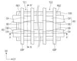
제 1 반도체 패턴들(NS1) 사이의 공간 및 제 2 반도체 패턴들(NS2) 사이의 공간을 실질적으로 동일할 수 있다. 제 1 영역(RG1)에서의 제 1 일함수 조절 패턴들(WF1)의 두께, 및 제 2 영역(RG2)에서의 제 1 일함수 조절 패턴들(WF1)의 두께는 실질적으로 동일할 수 있다. 따라서, 제 1 트랜지스터(TR1) 및 제 2 트랜지스터(TR2) 각각의 제 1 일함수 조절 패턴들(WF1)의 물질을 다르게 하여, 제 1 및 제 2 트랜지스터들(TR1, TR2)의 문턱 전압을 다르게 할 수 있다. 이 경우, 제 1 영역(RG1) 상에 제공되는 제 1 일함수 조절 패턴들(WF1)과 제 2 영역(RG2) 상에 제공되는 제 1 일함수 조절 패턴들(WF1)은 서로 다른 일함수를 갖는 실질적으로 다른 구성의 일함수 조절 패턴들일 수 있다.The space between the first semiconductor patterns (NS1) and the space between the second semiconductor patterns (NS2) can be substantially the same. The thickness of the first work function control patterns (WF1) in the first region (RG1) and the thickness of the first work function control patterns (WF1) in the second region (RG2) can be substantially the same. Accordingly, by making the materials of the first work function control patterns (WF1) of each of the first transistor (TR1) and the second transistor (TR2) different, the threshold voltages of the first and second transistors (TR1, TR2) can be made different. In this case, the first work function control patterns (WF1) provided on the first region (RG1) and the first work function control patterns (WF1) provided on the second region (RG2) can be work function control patterns having substantially different configurations and having different work functions.
다른 실시예들에 따르면, 제 1 영역(RG1) 및 제 2 영역(RG2)에서 각각 제 1 일함수 조절 패턴들(WF1)의 두께를 다르게 하여, 제 1 및 제 2 트랜지스터들(TR1, TR2)의 문턱 전압을 다르게 할 수 있다. 도 2a는 본 발명의 실시예들에 따른 반도체 장치를 설명하기 위한 평면도이다. 도 2b는 도 2a의 C-C'선에 따른 단면도이고, 도 2c는 도 2a의 D-D'선에 따른 단면도이다. 도 2a 내지 도 2c에 도시된 바와 같이, 제 1 영역(RG1) 상에서의 제 1 일함수 조절 패턴들(WF1')의 두께는 제 2 영역(RG2) 상에서의 제 1 일함수 조절 패턴들(WF1')의 두께보다 두꺼울 수 있다. 이때, 제 1 영역(RG1)의 제 1 일함수 조절 패턴(WF1')의 두께가 충분히 두꺼운 경우, 제 1 일함수 조절 패턴(WF1')은 제 1 반도체 패턴들(NS1) 사이의 공간을 채울 수 있다. 이에 따라, 제 2 일함수 조절 패턴(WF2) 및 게이트 전극(GE)은 제 1 반도체 패턴들(NS1) 사이로 연장되지 않을 수 있으며, 제 1 영역(RG1) 상의 채널 패턴(CH) 및 제 1 일함수 조절 패턴(WF1')을 전체적으로 둘러쌀 수 있다. 제 1 영역(RG1) 및 제 2 영역(RG2) 상에서 제 1 일함수 조절 패턴들(WF1')은 동일한 물질을 포함할 수 있다. 상기와 같이, 제 1 영역(RG1) 및 제 2 영역(RG2)의 일함수 조절 패턴들(WF1', WF2)의 두께를 달리하여, 제 1 및 제 2 트랜지스터들(TR1, RT2)의 문턱 전압을 다르게 조절할 수 있다. 이하, 도 1a 내지 도 1c의 실시예를 기준으로 계속 설명한다.According to other embodiments, the thicknesses of the first work function control patterns (WF1) in the first region (RG1) and the second region (RG2) may be made different, respectively, so that the threshold voltages of the first and second transistors (TR1, TR2) may be made different. FIG. 2A is a plan view illustrating a semiconductor device according to embodiments of the present invention. FIG. 2B is a cross-sectional view taken along line C-C' of FIG. 2A, and FIG. 2C is a cross-sectional view taken along line D-D' of FIG. 2A. As illustrated in FIGS. 2A to 2C, the thickness of the first work function control patterns (WF1') on the first region (RG1) may be thicker than the thickness of the first work function control patterns (WF1') on the second region (RG2). At this time, when the thickness of the first work function control pattern (WF1') of the first region (RG1) is sufficiently thick, the first work function control pattern (WF1') can fill the space between the first semiconductor patterns (NS1). Accordingly, the second work function control pattern (WF2) and the gate electrode (GE) may not extend between the first semiconductor patterns (NS1) and may entirely surround the channel pattern (CH) and the first work function control pattern (WF1') on the first region (RG1). The first work function control patterns (WF1') on the first region (RG1) and the second region (RG2) may include the same material. As described above, by varying the thickness of the work function control patterns (WF1', WF2) of the first region (RG1) and the second region (RG2), the threshold voltages of the first and second transistors (TR1, RT2) can be varied. Hereinafter, the description will continue based on the embodiments of FIGS. 1A to 1C.
기판(100)의 전면 상에 층간 절연막(120)이 제공될 수 있다. 층간 절연막(120)은 소자 분리막(ST), 제 1 및 제 2 게이트 구조체들(GS1, GS2) 및 소스/드레인 패턴들(SD)을 덮을 수 있다. 층간 절연막(120)의 상면은 게이트 캐핑 패턴들(CP)의 상면들과 실질적으로 공면을 이룰 수 있다. 층간 절연막(120)은 실리콘 산화물(SiO) 또는 실리콘 산질화물(SiON)을 포함할 수 있다.An interlayer insulating film (120) may be provided on the front surface of the substrate (100). The interlayer insulating film (120) may cover the element isolation film (ST), the first and second gate structures (GS1, GS2), and the source/drain patterns (SD). An upper surface of the interlayer insulating film (120) may be substantially coplanar with upper surfaces of the gate capping patterns (CP). The interlayer insulating film (120) may include silicon oxide (SiO) or silicon oxynitride (SiON).
도시되진 않았지만, 층간 절연막(120)을 관통하여 소스/드레인 패턴들(SD) 또는 게이트 구조체들(GS1, GS2)에 연결되는 콘택들(미도시)이 제공될 수 있다. 상기 콘택들(미도시)은 텅스텐(W), 티타늄(Ti), 탄탈륨(Ta)과 같은 금속 물질을 포함할 수 있다.Although not shown, contacts (not shown) may be provided that penetrate the interlayer insulating film (120) and are connected to source/drain patterns (SD) or gate structures (GS1, GS2). The contacts (not shown) may include a metal material such as tungsten (W), titanium (Ti), or tantalum (Ta).
도 3a 내지 도 11a는 본 발명의 실시예들에 따른 반도체 장치의 제조 방법을 설명하기 위한 평면도들이다. 도 3b 내지 도 11b는 각각 도 3a 내지 도 11a의 A-A'선에 따른 단면도들이다. 도 3c 내지 도 11c는 각각 도 3a 내지 도 11a의 B-B'선에 따른 단면도들이다. 설명의 편의를 위하여 도 3a 내지 도 11a에서 일부 구성은 생략하였다.FIGS. 3A to 11A are plan views for explaining a method of manufacturing a semiconductor device according to embodiments of the present invention. FIGS. 3B to 11B are cross-sectional views taken along line A-A' of FIGS. 3A to 11A, respectively. FIGS. 3C to 11C are cross-sectional views taken along line B-B' of FIGS. 3A to 11A, respectively. For convenience of explanation, some components are omitted from FIGS. 3A to 11A.
도 3a 내지 도 3c를 참조하여, 희생층들(150) 및 반도체층들(152)이 기판(100) 상에 교대로 그리고 반복적으로 적층될 수 있다. 도 3b 및 도 3c에서는 반도체층들(152)이 3개층으로 적층되는 것을 도시하였으나, 본 발명이 이에 한정되는 것은 아니다. 희생층들(150) 및 반도체층들(152)은 기판(100)을 시드층(seed layer)으로 하는 에피택시얼 성장(epitaxial growth) 공정을 통해 형성될 수 있다. 희생층들(150) 및 반도체층들(152)은 기판(100)의 전면 상에서 컨포멀하게 성장될 수 있다. 희생층들(150) 및 반도체층들(152)의 각각은 제 3 방향(D3)에 따른 두께를 가질 수 있다. 희생층들(150) 및 반도체층들(152)은 서로 동일한 두께를 가지도록 형성되거나, 서로 다른 두께를 가지도록 형성될 수 있다. 희생층들(150)의 각각의 두께는 약 1Å 내지 약 100nm의 범위에 있을 수 있고, 반도체층들(152)의 각각의 두께는 약 1Å 내지 약 100nm의 범위에 있을 수 있다. 희생층들(150)은 반도체층들(152)에 대해 식각 선택성을 갖는 실리콘 게르마늄(SiGe) 또는 게르마늄(Ge)을 포함하고, 반도체층들(152)은 실리콘(Si)을 포함할 수 있다.Referring to FIGS. 3A to 3C, sacrificial layers (150) and semiconductor layers (152) may be alternately and repeatedly laminated on a substrate (100). In FIGS. 3B and 3C, the semiconductor layers (152) are laminated in three layers, but the present invention is not limited thereto. The sacrificial layers (150) and the semiconductor layers (152) may be formed through an epitaxial growth process using the substrate (100) as a seed layer. The sacrificial layers (150) and the semiconductor layers (152) may be conformally grown on the entire surface of the substrate (100). Each of the sacrificial layers (150) and the semiconductor layers (152) may have a thickness along the third direction (D3). The sacrificial layers (150) and the semiconductor layers (152) may be formed to have the same thickness or may be formed to have different thicknesses. The thickness of each of the sacrificial layers (150) may be in a range of about 1 Å to about 100 nm, and the thickness of each of the semiconductor layers (152) may be in a range of about 1 Å to about 100 nm. The sacrificial layers (150) may include silicon germanium (SiGe) or germanium (Ge) having etch selectivity with respect to the semiconductor layers (152), and the semiconductor layers (152) may include silicon (Si).
필요에 따라, 반도체층들(152)에 불순물이 도핑될 수 있다. 예를 들어, 제 1 및 제 2 트랜지스터들(TR1, TR2)을 NMOFET으로 형성하고자 하는 경우, 상기 불순물은 보론(B)일 수 있다. 제 1 및 제 2 트랜지스터들(TR1, TR2)을 PMOSFET으로형성하고자 하는 경우, 상기 불순물은 인(P)일 수 있다. 만약, 제 1 및 제 2 트랜지스터들(TR1, TR2)을 서로 다른 도전형을 갖도록 형성하고자 하는 경우, 반도체층들(152)은 제 1 영역(RG1) 및 제 2 영역(RG2)에서 서로 다른 불순물이 도핑될 수 있다.If necessary, the semiconductor layers (152) may be doped with impurities. For example, if the first and second transistors (TR1, TR2) are to be formed as NMOFETs, the impurity may be boron (B). If the first and second transistors (TR1, TR2) are to be formed as PMOSFETs, the impurity may be phosphorus (P). If the first and second transistors (TR1, TR2) are to be formed to have different conductivity types, the semiconductor layers (152) may be doped with different impurities in the first region (RG1) and the second region (RG2).
기판(100) 상에 예비 활성 패턴들(PAP) 및 기저 활성 패턴들(102)이 형성될 수 있다. 예비 활성 패턴들(PAP) 및 기저 활성 패턴들(102)을 형성하는 것은, 희생층들(150), 반도체층들(152), 및 기판(100)의 상부를 차례로 패터닝하여 예비 활성 패턴들(PAP) 및 기저 활성 패턴들(102)을 정의하는 트렌치들(T)을 형성하는 것을 포함할 수 있다. 트렌치들(T)은 제 1 방향(D1)으로 연장되는 라인 형태일 수 있고, 제 2 방향(D2)으로 서로 이격될 수 있다. 예비 활성 패턴들(PAP)은 기저 활성 패턴들(102) 상에 각각 배치될 수 있다. 예비 활성 패턴들(PAP)은 제 1 방향(D1)으로 연장되는 라인 또는 바 형태로 형성될 수 있다.Preliminary active patterns (PAP) and base active patterns (102) may be formed on a substrate (100). Forming the preliminary active patterns (PAP) and base active patterns (102) may include sequentially patterning the sacrificial layers (150), the semiconductor layers (152), and the upper portion of the substrate (100) to form trenches (T) defining the preliminary active patterns (PAP) and base active patterns (102). The trenches (T) may have a line shape extending in a first direction (D1) and may be spaced apart from each other in a second direction (D2). The preliminary active patterns (PAP) may be respectively arranged on the base active patterns (102). The preliminary active patterns (PAP) may be formed in a line or bar shape extending in the first direction (D1).
트렌치들(T)을 채우는 소자 분리막(ST)이 형성될 수 있다. 소자 분리막(ST)을 형성하는 것은, 기판(100)의 전면 상에 절연막을 형성하고, 예비 활성 패턴들(PAP)이 완전히 노출되도록 상기 절연막을 리세스하는 것을 포함할 수 있다. 이로써, 소자 분리막(ST)의 상면은 기저 활성 패턴들(102)의 상면들보다 더 낮을 수 있다.A device isolation film (ST) may be formed to fill the trenches (T). Forming the device isolation film (ST) may include forming an insulating film on the entire surface of the substrate (100) and recessing the insulating film so that the preliminary active patterns (PAP) are fully exposed. As a result, an upper surface of the device isolation film (ST) may be lower than the upper surfaces of the underlying active patterns (102).
도 4a 내지 도 4c를 참조하여, 희생 게이트 구조체들(SGS)이 상기 예비 활성 패턴들(PAP)을 가로지르도록 형성될 수 있다. 희생 게이트 구조체들(SGS)은 제 2 방향(D2)으로 연장되어 기저 활성 패턴들(102) 및 소자 분리막(ST)을 가로를 수 있다. 희생 게이트 구조체들(SGS)은 기판(100) 상에 차례로 적층되는 희생 게이트 패턴(162) 및 게이트 마스크 패턴(164)을 포함할 수 있다. 희생 게이트 패턴(162) 및 게이트 마스크 패턴(164)은 기판(100) 상에 희생 게이트막 및 게이트 마스크막을 순차적으로 형성한 후, 이들을 순차적으로 패터닝하여 형성될 수 있다. 상기 희생 게이트막은 폴리 실리콘(poly Si)을 포함할 수 있다. 상기 게이트 마스크막은 실리콘 질화물(SiN) 또는 실리콘 산질화물(SiON)을 포함할 수 있다. 희생 게이트 구조체들(SGS)은 제 2 방향(D2)으로 연장되는 라인 형태일 수 있다. 희생 게이트 구조체들(SGS)은 예비 활성 패턴들(PAP)의, 제 2 방향(D2)으로 서로 마주하는, 측면들을 덮을 수 있고, 예비 활성 패턴들(PAP)의 상면 및 소자 분리막(ST)의 상면들을 덮을 수 있다.Referring to FIGS. 4A to 4C, sacrificial gate structures (SGS) may be formed to cross the preliminary active patterns (PAP). The sacrificial gate structures (SGS) may extend in the second direction (D2) to cross the base active patterns (102) and the device isolation film (ST). The sacrificial gate structures (SGS) may include a sacrificial gate pattern (162) and a gate mask pattern (164) that are sequentially stacked on a substrate (100). The sacrificial gate pattern (162) and the gate mask pattern (164) may be formed by sequentially forming a sacrificial gate film and a gate mask film on the substrate (100) and then sequentially patterning them. The sacrificial gate film may include polysilicon (poly Si). The gate mask film may include silicon nitride (SiN) or silicon oxynitride (SiON). The sacrificial gate structures (SGS) may be in the form of lines extending in the second direction (D2). The sacrificial gate structures (SGS) may cover side surfaces of the preliminary active patterns (PAP) facing each other in the second direction (D2), and may cover upper surfaces of the preliminary active patterns (PAP) and upper surfaces of the device isolation film (ST).
희생 게이트 구조체들(SGS)은 게이트 스페이서들(GSP)를 더 포함할 수 있다. 한 쌍의 게이트 스페이서들(GSP)은 희생 게이트 구조체들(SGS) 각각의 양 측벽들 상에 각각 형성될 수 있다. 게이트 스페이서들(GSP)은 실리콘 탄질화물(SiCN), 실리콘 탄소 산질화물(SiCON) 또는 실리콘 질화물(SiN)을 이용하여 형성될 수 있다. 게이트 스페이서들(GSP)을 형성하는 것은, CVD 또는 ALD와 같은 증착 공정으로 스페이서막을 형성하는 것, 및 상기 스페이서막에 이방성 식각 공정을 수행하는 것을 포함할 수 있다.The sacrificial gate structures (SGS) may further include gate spacers (GSP). A pair of gate spacers (GSP) may be formed on each of the two sidewalls of the sacrificial gate structures (SGS). The gate spacers (GSP) may be formed using silicon carbon nitride (SiCN), silicon carbon oxynitride (SiCON), or silicon nitride (SiN). Forming the gate spacers (GSP) may include forming a spacer film by a deposition process such as CVD or ALD, and performing an anisotropic etching process on the spacer film.
도 5a 내지 도 5c를 참조하여, 예비 활성 패턴들(PAP)을 패터닝하여, 채널 패턴들(CH)이 형성될 수 있다. 예비 활성 패턴들(PAP)은 게이트 마스크 패턴들(164) 및 게이트 스페이서들(GSP)을 식각 마스크로 하여 패터닝될 수 있다. 이로써, 게이트 마스크 패턴들(164) 및 게이트 스페이서들(GSP)에 의해 기저 활성 패턴들(102)의 일부가 노출될 수 있다.Referring to FIGS. 5A to 5C, channel patterns (CH) can be formed by patterning preliminary active patterns (PAP). The preliminary active patterns (PAP) can be patterned using gate mask patterns (164) and gate spacers (GSP) as etching masks. As a result, a portion of the underlying active patterns (102) can be exposed by the gate mask patterns (164) and the gate spacers (GSP).
구체적으로, 예비 활성 패턴들(PAP)의 희생층들(150)이 패터닝되어 희생 패턴들(156)이 형성될 수 있다. 예비 활성 패턴들(PAP)의 반도체층들(152)이 패터닝되어 제 1 및 제 2 반도체 패턴들(NS1, NS2)이 형성될 수 있다. 제 1 반도체 패턴들(NS1)은 제 1 영역(RG1)의 채널 패턴(CH)을 구성할 수 있고, 제 2 반도체 패턴들(NS2)은 제 2 영역(RG2)의 채널 패턴(CH)을 구성할 수 있다.Specifically, sacrificial layers (150) of the preliminary active patterns (PAP) can be patterned to form sacrificial patterns (156). Semiconductor layers (152) of the preliminary active patterns (PAP) can be patterned to form first and second semiconductor patterns (NS1, NS2). The first semiconductor patterns (NS1) can form a channel pattern (CH) of the first region (RG1), and the second semiconductor patterns (NS2) can form a channel pattern (CH) of the second region (RG2).
상기 패터닝 공정 이후 노출된 희생 패턴들(156)의 일부가 수평적으로 제거되어, 함몰 영역들(112)이 형성될 수 있다. 함몰 영역들(112)을 형성하는 것은, 희생 패턴들(156)에 대하여 식각 선택성 있는 식각 소스로 식각 공정을 수행하는 것을 포함할 수 있다.After the above patterning process, a portion of the exposed sacrificial patterns (156) may be removed horizontally to form recessed regions (112). Forming the recessed regions (112) may include performing an etching process with an etching source that is selective for the sacrificial patterns (156).
함몰 영역들(112)을 채우는 스페이서 패턴들(110)이 형성될 수 있다. 스페이서 패턴들(110)은 제 1 및 제 2 반도체 패턴들(NS1, NS2)을 사이에 두고 서로 수직적으로 이격되도록 형성될 수 있다. 구체적으로, 기판(100)의 전면 상에 절연막을 컨포멀하게 형성할 수 있다. 상기 절연막은 함몰 영역들(112)을 채울 수 있다. 이어서, 함몰 영역들(112) 내에만 국소적으로 스페이서 패턴들(110)이 잔류할 때까지 상기 절연막을 식각할 수 있다.Spacer patterns (110) can be formed to fill the recessed regions (112). The spacer patterns (110) can be formed to be vertically spaced apart from each other with the first and second semiconductor patterns (NS1, NS2) interposed therebetween. Specifically, an insulating film can be conformally formed on the entire surface of the substrate (100). The insulating film can fill the recessed regions (112). Subsequently, the insulating film can be etched until the spacer patterns (110) remain locally only within the recessed regions (112).
채널 패턴들(CH) 각각의 양 측에 소스/드레인 패턴들(SD)이 형성될 수 있다. 구체적으로, 제 1 및 제 2 반도체 패턴들(NS1, NS2) 및 기저 활성 패턴들(102)을 씨드층으로 선택적 에피택시얼 공정을 수행하여, 소스/드레인 패턴들(SD)이 형성될 수 있다. 채널 패턴들(CH) 및 소스/드레인 패턴들(SD)은 서로 연결될 수 있다.Source/drain patterns (SD) may be formed on both sides of each of the channel patterns (CH). Specifically, the source/drain patterns (SD) may be formed by performing a selective epitaxial process using the first and second semiconductor patterns (NS1, NS2) and the base active patterns (102) as a seed layer. The channel patterns (CH) and the source/drain patterns (SD) may be connected to each other.
실시예들에서, 소스/드레인 패턴들(SD)은 채널 패턴(CH)과 동일한 반도체 원소(예를 들어, 실리콘(Si))로 형성될 수 있다. 상기 선택적 에피택시얼 공정과 동시에 또는 선택적 에피택시얼 공정 후, 소스/드레인 패턴들(SD)에 N형의 불순물이 도핑될 수 있다. 또는, 소스/드레인 패턴들(SD)은 실리콘(Si)보다 격자 상수가 큰 실리콘 게르마늄(SiGe)로 형성될 수 있다. 상기 선택적 에피택시얼 공정과 동시에 또는 선택적 에피택시얼 공정 후, 소스/드레인 패턴들(SD)에 P형의 불순물이 도핑될 수 있다.In embodiments, the source/drain patterns (SD) may be formed of the same semiconductor element (e.g., silicon (Si)) as the channel pattern (CH). At the same time as or after the selective epitaxial process, the source/drain patterns (SD) may be doped with N-type impurities. Alternatively, the source/drain patterns (SD) may be formed of silicon germanium (SiGe) having a lattice constant larger than that of silicon (Si). At the same time as or after the selective epitaxial process, the source/drain patterns (SD) may be doped with P-type impurities.
도 6a 내지 도 6c를 참조하여, 기판(100)의 전면 상에 층간 절연막(120)이 형성될 수 있다. 이어서, 희생 게이트 패턴들(162)의 상면들이 노출될 때까지 층간 절연막(120)을 평탄화하는 공정이 수행될 수 있다. 평탄화 공정은 에치백(etch back) 및/또는 CMP(chemical mechanical polishing) 공정을 포함할 수 있다. 층간 절연막(120)을 평탄화할 때, 게이트 마스크 패턴들(164)이 함께 제거될 수 있다. 층간 절연막(120)은 실리콘 산화물(SiO) 또는 실리콘 산질화물(SiON)을 이용하여 형성될 수 있다.Referring to FIGS. 6A to 6C, an interlayer insulating film (120) may be formed on the front surface of the substrate (100). Subsequently, a process of planarizing the interlayer insulating film (120) may be performed until the upper surfaces of the sacrificial gate patterns (162) are exposed. The planarization process may include an etch back and/or a chemical mechanical polishing (CMP) process. When planarizing the interlayer insulating film (120), the gate mask patterns (164) may be removed together. The interlayer insulating film (120) may be formed using silicon oxide (SiO) or silicon oxynitride (SiON).
상기 평탄화 공정에 의하여 노출된 희생 게이트 패턴들(162)이 선택적으로 제거될 수 있다. 희생 게이트 패턴들(162)이 제거됨에 따라, 기판(100)의 제 1 및 제 2 영역들(RG1, RG2) 상에 제 1 및 제 2 트렌치들(TC1, TC2)이 각각 형성될 수 있다. 제 1 및 제 2 트렌치들(TC1, TC2)은 게이트 스페이서들(GSP)에 의해 정의되는 빈 영역일 수 있다. 제 1 및 제 2 트렌치들(TC1, TC2)은 채널 패턴들(CH)을 노출시킬 수 있다. 제 1 및 제 2 트렌치들(TC1, TC2)은 희생 패턴들(156)을 노출시킬 수 있다. 제 1 및 제 2 트렌치들(TC1, TC2)은 평면적 관점에서, 제 2 방향(D2)으로 연장되는 라인 형태일 수 있고, 소자 분리막(ST)의 상면을 노출할 수 있다.The sacrificial gate patterns (162) exposed by the above planarization process can be selectively removed. As the sacrificial gate patterns (162) are removed, first and second trenches (TC1, TC2) can be formed on the first and second regions (RG1, RG2) of the substrate (100), respectively. The first and second trenches (TC1, TC2) can be empty regions defined by gate spacers (GSP). The first and second trenches (TC1, TC2) can expose the channel patterns (CH). The first and second trenches (TC1, TC2) can expose the sacrificial patterns (156). The first and second trenches (TC1, TC2) may be in the form of lines extending in the second direction (D2) in a planar view and may expose the upper surface of the element isolation film (ST).
노출된 희생 패턴들(156)이 선택적으로 제거될 수 있다. 예를 들어, 희생 패턴들(156)이 실리콘 게르마늄(SiGe)을 포함하고, 제 1 및 제 2 반도체 패턴들(NS1, NS2)이 실리콘(Si)를 포함하는 경우, 선택적 식각 공정은 과초산(peracetic acid)을 포함하는 식각액을 사용하여 수행될 수 있다. 이때, 소스/드레인 패턴들(SD)은 스페이서 패턴들(110) 및 층간 절연막(120)에 의하여 커버되어 보호될 수 있다. 희생 패턴들(156)이 선택적으로 제거됨에 따라, 제 1 및 제 2 영역들(RG1, RG2) 상에 제 1 공간들(SP1) 및 제 2 공간들(SP2)이 형성될 수 있다. 제 1 공간(SP1)은 서로 수직적으로 인접하는 반도체 패턴들(NS1, NS2) 사이의 공간일 수 있다. 제 2 공간(SP2)은 한 쌍의 게이트 스페이서들(GSP) 및 최상부의 반도체 패턴(NS1, NS2)에 의해 둘러싸인 공간일 수 있다. 제 1 및 제 2 공간들(SP1, SP2)은 제 1 및 제 2 트렌치들(TC1, TC2)과 연통되어, 제 1 및 제 2 반도체 패턴들(NS1, NS2)을 노출시킬 수 있다.The exposed sacrificial patterns (156) can be selectively removed. For example, when the sacrificial patterns (156) include silicon germanium (SiGe) and the first and second semiconductor patterns (NS1, NS2) include silicon (Si), the selective etching process can be performed using an etchant including peracetic acid. At this time, the source/drain patterns (SD) can be covered and protected by the spacer patterns (110) and the interlayer insulating film (120). As the sacrificial patterns (156) are selectively removed, first spaces (SP1) and second spaces (SP2) can be formed on the first and second regions (RG1, RG2). The first space (SP1) can be a space between the semiconductor patterns (NS1, NS2) that are vertically adjacent to each other. The second space (SP2) may be a space surrounded by a pair of gate spacers (GSP) and a top semiconductor pattern (NS1, NS2). The first and second spaces (SP1, SP2) may be connected to the first and second trenches (TC1, TC2) to expose the first and second semiconductor patterns (NS1, NS2).
도 7a 내지 도 7c를 참조하여, 제 1 및 제 2 트렌치들(TC1, TC2)을 통해 노출된 제 1 및 제 2 반도체 패턴들(NS1, NS2) 상에 게이트 유전막들(GI)이 형성될 수 있다. 게이트 유전막들(GI)은 제 1 및 제 2 트렌치들(TC1, TC2)의 내면들을 컨포멀하게 덮도록 형성될 수 있다. 각각의 게이트 유전막들(GI)은 제 1 및 제 2 트렌치들(TC1, TC2)의 제 1 공간들(SP1)을 부분적으로 채울 수 있다. 각각의 게이트 유전막들(GI)은 제 1 및 제 2 트렌치들(TC1, TC2)의 제 2 공간들(SP2)을 부분적으로 채울 수 있다. 게이트 유전막들(GI)은 스페이서 패턴들(110) 및 제 1 및 제 2 반도체 패턴들(NS1, NS2)을 직접 덮을 수 있다. 게이트 유전막들(GI)은 실리콘 산화물(SiO)보다 높은 고유전 물질을 이용하여 형성될 수 있다.Referring to FIGS. 7A to 7C, gate dielectric films (GI) may be formed on the first and second semiconductor patterns (NS1, NS2) exposed through the first and second trenches (TC1, TC2). The gate dielectric films (GI) may be formed to conformally cover inner surfaces of the first and second trenches (TC1, TC2). Each of the gate dielectric films (GI) may partially fill the first spaces (SP1) of the first and second trenches (TC1, TC2). Each of the gate dielectric films (GI) may partially fill the second spaces (SP2) of the first and second trenches (TC1, TC2). The gate dielectric films (GI) may directly cover the spacer patterns (110) and the first and second semiconductor patterns (NS1, NS2). Gate dielectric films (GI) can be formed using high-k materials higher than silicon oxide (SiO).
도시하지는 않았으나, 게이트 유전막들(GI)을 형성하기 전에, 제 1 및 제 2 트렌치들(TC1, TC2)을 통해 노출된 제 1 및 제 2 반도체 패턴들(NS1, NS2) 상에 플라즈마를 이용한 산화 공정이 수행될 수 있다. 이를 통해, 노출된 제 1 및 제 2 반도체 패턴들(NS1, NS2)로부터 계면막들(미도시)이 성장될 수 있다. 상기 계면막들(미도시)을 형성하는 것은, 열적 산화(Thermal Oxidation) 및/또는 화학적 산화(Chemical Oxidation) 공정을 포함할 수 있다. 상기 산화 공정은 산소, 오존 및 수증기 중 적어도 하나의 플라즈마를 이용할 수 있다. 상기 계면막들(미도시)은 실리콘 산화물(SiO)을 이용하여 형성될 수 있다. 상기 계면막들(미도시)은 노출된 제 1 및 제 2 반도체 패턴들(NS1, NS2)의 표면들을 직접 감쌀 수 있다.Although not illustrated, before forming the gate dielectric films (GI), an oxidation process using plasma may be performed on the first and second semiconductor patterns (NS1, NS2) exposed through the first and second trenches (TC1, TC2). Through this, interface films (not illustrated) may be grown from the exposed first and second semiconductor patterns (NS1, NS2). Forming the interface films (not illustrated) may include a thermal oxidation process and/or a chemical oxidation process. The oxidation process may use plasma of at least one of oxygen, ozone, and water vapor. The interface films (not illustrated) may be formed using silicon oxide (SiO). The interface films (not illustrated) may directly surround surfaces of the exposed first and second semiconductor patterns (NS1, NS2).
도 8a 내지 도 8c를 참조하여, 제 1 및 제 2 트랜치들(TC1, TC2) 내에 제 1 일함수 조절막(WL1)이 컨포멀하게 증착될 수 있다. 제 1 일함수 조절막(WL1)은 ALD, CVD 또는 PVD와 같은 증착 공정을 통해 형성될 수 있다. 제 1 일함수 조절막(WL1)은 게이트 유전막들(GI)을 컨포멀하게 덮을 수 있다. 제 1 일함수 조절막(WL1)은 제 1 및 제 2 반도체 패턴들(NS1, NS2)을 둘러싸도록 형성될 수 있다. 제 1 일함수 조절막(WL1)은 상대적으로 낮은 일함수를 갖는 물질을 포함할 수 있다. 예를 들어, 제 1 일함수 조절막(WL1)은 티타늄 알루미늄 탄화물(TiAlC), 티타늄 알루미늄 질화물(TiAlN) 또는 탄탈 알루미늄 질화물(TaAlN)을 포함할 수 있다.Referring to FIGS. 8A to 8C, a first work function control film (WL1) may be conformally deposited within the first and second trenches (TC1, TC2). The first work function control film (WL1) may be formed through a deposition process such as ALD, CVD, or PVD. The first work function control film (WL1) may conformally cover the gate dielectric films (GI). The first work function control film (WL1) may be formed to surround the first and second semiconductor patterns (NS1, NS2). The first work function control film (WL1) may include a material having a relatively low work function. For example, the first work function control film (WL1) may include titanium aluminum carbide (TiAlC), titanium aluminum nitride (TiAlN), or tantalum aluminum nitride (TaAlN).
다른 실시예들에 따르면, 제 1 일함수 조절막(WL1)이 형성된 후, 제 1 영역(RG1) 상에서 제 1 일함수 조절막(WL1)이 추가로 증착될 수 있다. 도 9a 내지 도 9c에 도시된 바와 같이, 제 2 영역(RG2) 상에 마스크 패턴(MP)이 형성될 수 있다. 마스크 패턴(MP)은 제 1 영역(RG1)을 노출시킬 수 있다. 제 1 영역(RG1) 상에서 노출된 제 1 일함수 조절막(WL1) 상에 상기 증착 공정이 추가로 수행될 수 있다. 이에 따라, 제 1 영역(RG1)의 제 1 일함수 조절막(WL1')은 제 2 영역(RG2)의 제 1 일함수 조절막(WL1)보다 더 두꺼운 두께를 갖도록 형성될 수 있다. 또는, 제 1 영역(RG1) 및 제 2 영역(RG2) 상에서 두꺼운 두께의 일함수 조절막(WL1)을 형성한 후, 제 1 영역(RG1) 상에 마스크 패턴을 형성하고, 제 2 영역(RG2) 상의 제 1 일함수 조절막(WL1)의 상부를 제거할 수도 있다. 이 경우, 도 2a 내지 도 2c를 참조하여 설명한 반도체 장치가 제조될 수 있다.According to other embodiments, after the first work function control film (WL1) is formed, a first work function control film (WL1) may be additionally deposited on the first region (RG1). As illustrated in FIGS. 9A to 9C, a mask pattern (MP) may be formed on the second region (RG2). The mask pattern (MP) may expose the first region (RG1). The deposition process may be additionally performed on the first work function control film (WL1) exposed on the first region (RG1). Accordingly, the first work function control film (WL1') of the first region (RG1) may be formed to have a thicker thickness than the first work function control film (WL1) of the second region (RG2). Alternatively, after forming a thick work function control film (WL1) on the first region (RG1) and the second region (RG2), a mask pattern may be formed on the first region (RG1), and an upper portion of the first work function control film (WL1) on the second region (RG2) may be removed. In this case, the semiconductor device described with reference to FIGS. 2A to 2C can be manufactured.
이와는 또 다르게, 제 1 영역(RG1) 및 제 2 영역(RG2)에서 제 1 일함수 조절막(WL1)이 서로 다른 물질을 갖도록 형성될 수 있다. 예를 들어, 제 1 일함수 조절막(WL1)을 형성한 후, 제 2 영역(RG2) 상에 마스크 패턴(MP)이 형성될 수 있다. 제 1 영역(RG1) 상에서 노출되는 제 1 일함수 조절막(WL1)이 제거될 수 있다. 이후, 상기 제 1 영역(RG1) 상에 제 2 영역(RG2)의 제 1 일함수 조절막(WL1)과는 다른 물질을 이용하여 증착 공정이 수행될 수 있다. 이 경우, 제 1 영역(RG1)에 형성되는 제 1 트랜지스터들(TR1)과 제 2 영역(RG2)에 형성되는 제 2 트랜지스터들(TR2)은 서로 다른 타입으로 제공될 수 있다.Alternatively, the first work function control film (WL1) in the first region (RG1) and the second region (RG2) may be formed to have different materials. For example, after forming the first work function control film (WL1), a mask pattern (MP) may be formed on the second region (RG2). The first work function control film (WL1) exposed on the first region (RG1) may be removed. Thereafter, a deposition process may be performed on the first region (RG1) using a different material from the first work function control film (WL1) of the second region (RG2). In this case, the first transistors (TR1) formed in the first region (RG1) and the second transistors (TR2) formed in the second region (RG2) may be provided as different types.
이하, 도 8a 내지 8c의 실시예를 기준으로 계속 설명하도록 한다.Below, the explanation will continue based on the examples of Figs. 8a to 8c.
도 10a 내지 도 10c를 참조하여, 제 1 및 제 2 트랜치들(TC1, TC2) 내에 제 2 일함수 조절막(WL2)이 형성될 수 있다. 제 2 일함수 조절막(WL2)은 제 1 및 제 2 트랜치들(TC1, TC2) 내에 컨포멀하게 증착될 수 있다. 제 2 일함수 조절막(WL2)은 ALD, CVD 또는 PVD와 같은 증착 공정을 통해 형성될 수 있다. 제 2 일함수 조절막(WL2)은 제 1 일함수 조절막(WL1)을 컨포멀하게 덮을 수 있다. 제 2 일함수 조절막(WL2)은 상대적으로 높은 일함수를 갖는 물질을 포함할 수 있다. 예를 들어, 제 2 일함수 조절막(WL2)은 티타늄 질화물(TiN), 티타늄 산질화물(TiON) 또는 탄탈 질화물(TaN)을 포함할 수 있다.Referring to FIGS. 10A to 10C, a second work function control film (WL2) may be formed within the first and second trenches (TC1, TC2). The second work function control film (WL2) may be conformally deposited within the first and second trenches (TC1, TC2). The second work function control film (WL2) may be formed through a deposition process such as ALD, CVD, or PVD. The second work function control film (WL2) may conformally cover the first work function control film (WL1). The second work function control film (WL2) may include a material having a relatively high work function. For example, the second work function control film (WL2) may include titanium nitride (TiN), titanium oxynitride (TiON), or tantalum nitride (TaN).
제 1 일함수 조절막(WL1)을 형성하는 제 1 공정(S1)과 제 2 일함수 조절막(WL2)을 형성하는 제 2 공정(S2)은 인-시츄(in-situ) 공정으로 수행될 수 있다. 즉, 제 2 공정(S2)은 제 1 공정(S1)과 동일한 공정 챔버 내에서 연속적으로 수행될 수 있다. 여기서, 연속적으로 수행됨이라 함은 공정 기안, 공정 온도 및 상기 공정 챔버 내의 분위기 가스와 같은 공정 조건이 동일하게 유지되는 상태에서 복수의 공정이 수행되는 것을 의미한다. 더하여, 제 1 공정(S1) 및 제 2 공정(S2)은 진공 분위기 또는 무산소(oxygen free) 분위기 하에서 수행될 수 있다.The first process (S1) for forming the first work function control film (WL1) and the second process (S2) for forming the second work function control film (WL2) can be performed as in-situ processes. That is, the second process (S2) can be performed continuously in the same process chamber as the first process (S1). Here, performing continuously means that a plurality of processes are performed in a state where process conditions such as process design, process temperature, and atmospheric gas in the process chamber are maintained the same. In addition, the first process (S1) and the second process (S2) can be performed in a vacuum atmosphere or an oxygen free atmosphere.
일반적으로, 대량 생산 시스템에서의 효율성을 위하여, 제 1 일함수 조절막(WL1)을 형성하는 제 1 공정(S1)과 제 2 일함수 조절막(WL2)을 형성하는 제 2 공정(S2)은 별개의 챔버에서 수행될 수 있다. 예를 들어, 제 1 챔버에서 제 1 일함수 조절막(WL1)을 형성하는 제 1 공정(S1)이 수행되고, 제 2 챔버에서 제 2 일함수 조절막(WL2)을 형성하는 제 2 공정(S2)이 수행될 수 있다. 이 경우, 제조 중인 반도체 장치가 상기 제 1 챔버에서 상기 제 2 챔버로 이송되면서, 제 1 일함수 조절막(WL1)이 산소와 접할 수 있다. 이때, 도 11a 내지 도 11c에 도시된 바와 같이, 제 1 일함수 조절막(WL1)의 노출되는 면들이 산화되어 제 1 일함수 조절막(WL1) 상에 산화막(OL)이 형성될 수 있다. 특히, 제 1 일함수 조절막(WL1)이 알루미늄(Al)과 같이 산소와의 반응성이 높은 물질을 포함하는 경우, 산화막(OL)의 형성이 가속화될 수 있다. 이 경우, 제 1 일함수 조절막(WL1)의 일부가 산화막(OL)을 형성하여 제 1 일함수 조절막(WL1)의 두께가 감소하거나, 또는 제 1 일함수 조절막(WL1)을 이루는 물질이 산화막(OL)으로 확산되어, 제 1 일함수 조절막(WL1)의 일함수가 증가할 수 있다. 이는, 트랜지스터들(TR1, TR2)의 문턱 전압의 조절에 문제점으로 작용할 수 있다.In general, for efficiency in a mass production system, the first process (S1) for forming the first work function control film (WL1) and the second process (S2) for forming the second work function control film (WL2) may be performed in separate chambers. For example, the first process (S1) for forming the first work function control film (WL1) may be performed in a first chamber, and the second process (S2) for forming the second work function control film (WL2) may be performed in a second chamber. In this case, when the semiconductor device being manufactured is transferred from the first chamber to the second chamber, the first work function control film (WL1) may come into contact with oxygen. At this time, as illustrated in FIGS. 11A to 11C, the exposed surfaces of the first work function control film (WL1) may be oxidized to form an oxide film (OL) on the first work function control film (WL1). In particular, when the first work function control film (WL1) includes a material having a high reactivity with oxygen, such as aluminum (Al), the formation of the oxide film (OL) may be accelerated. In this case, a part of the first work function control film (WL1) may form the oxide film (OL), thereby reducing the thickness of the first work function control film (WL1), or a material forming the first work function control film (WL1) may diffuse into the oxide film (OL), thereby increasing the work function of the first work function control film (WL1). This may cause a problem in controlling the threshold voltage of the transistors (TR1, TR2).
더하여, 제 1 일함수 조절막(WL1) 상에 산화막(OL)과 같은 다른 물질층 이 형성되는 경우, 제 1 일함수 조절막(WL1)과 후에 형성되는 제 2 일함수 조절막(WL2)은 서로 접하지 않도록 형성될 수 있다. 즉, 제 1 및 제 2 일함수 조절막들(WL1, WL2) 사이에 산화막(OL)이 개재될 수 있다. 이 경우, 제 1 및 제 2 일함수 조절막들(WL1, WL2) 사이의 전기 저항이 증가할 수 있으며, 반도체 장치의 전기적 특성이 저하될 수 있다.In addition, when another material layer, such as an oxide film (OL), is formed on the first work function control film (WL1), the first work function control film (WL1) and the second work function control film (WL2) formed later may be formed so as not to contact each other. That is, an oxide film (OL) may be interposed between the first and second work function control films (WL1, WL2). In this case, the electrical resistance between the first and second work function control films (WL1, WL2) may increase, and the electrical characteristics of the semiconductor device may deteriorate.
본 발명에 따르면, 제 1 공정(S1)과 제 2 공정(S2)은 인-시츄(in-situ) 공정으로 수행될 수 있으며, 상기 인-시츄 공정이 수행되는 챔버는 진공 분위기 또는 무산소(oxygen free) 분위기일 수 있다. 이에 따라, 제 1 일함수 조절막(WL1)이 외부 산소와 접하지 않을 수 있으며, 제 1 일함수 조절막(WL1) 상에 산화막과 같은 다른 물질층이 형성되지 않을 수 있다. 이때, 제 1 일함수 조절막(WL1) 내에 함유되는 산소(O)의 양은 실질적으로 없거나, 0% 내지 30%일 수 있다. 제 2 일함수 조절막(WL2)을 형성하기 전의 제 1 일함수 조절막(WL1) 내의 알루미늄(Al) 함량은 제 2 일함수 조절막(WL2)을 형성한 후의 제 1 일함수 조절막(WL1) 내의 알루미늄(Al) 함량과 실질적으로 동일할 수 있다. 제 1 일함수 조절막(WL1)의 손실이 없어, 트랜지스터들(TR1, TR2)의 문턱 전압의 조절이 용이할 수 있으며, 제 1 및 제 2 일함수 조절막들(WL1, WL2)이 직접적으로 접하여, 반도체 장치의 전기적 특성이 저하되지 않을 수 있다.According to the present invention, the first process (S1) and the second process (S2) can be performed as an in-situ process, and the chamber in which the in-situ process is performed can be a vacuum atmosphere or an oxygen free atmosphere. Accordingly, the first work function control film (WL1) may not come into contact with external oxygen, and another material layer such as an oxide film may not be formed on the first work function control film (WL1). At this time, the amount of oxygen (O) contained in the first work function control film (WL1) may be substantially none, or 0% to 30%. The aluminum (Al) content in the first work function control film (WL1) before forming the second work function control film (WL2) may be substantially the same as the aluminum (Al) content in the first work function control film (WL1) after forming the second work function control film (WL2). Since there is no loss of the first work function control film (WL1), the threshold voltage of the transistors (TR1, TR2) can be easily controlled, and since the first and second work function control films (WL1, WL2) are in direct contact, the electrical characteristics of the semiconductor device may not be deteriorated.
다른 실시예들에 따르면, 제 1 챔버에서 제 1 일함수 조절막(WL1)을 형성하는 제 1 공정(S1)이 수행되고, 제 2 챔버에서 제 2 일함수 조절막(WL2)을 형성하는 제 2 공정(S2)이 수행될 수 있다. 이때, 제 1 일함수 조절막(WL1) 상에 산화막(OL)이 형성될 수 있다. 이후, 제조중인 반도체 장치는 제 2 챔버로 이송될 수 있으며, 제 2 일함수 조절막(WL2)을 형성하기 전에, 제 2 챔버 내에서 산화막(OL)을 제거하는 공정이 수행될 수 있다. 이에 따라, 제 1 일함수 조절막(WL1) 상에 제 2 일함수 조절막(WL2)이 직접적으로 접하도록 형성될 수 있다.According to other embodiments, a first process (S1) of forming a first work function control film (WL1) may be performed in a first chamber, and a second process (S2) of forming a second work function control film (WL2) may be performed in a second chamber. At this time, an oxide film (OL) may be formed on the first work function control film (WL1). Thereafter, the semiconductor device being manufactured may be transferred to the second chamber, and before forming the second work function control film (WL2), a process of removing the oxide film (OL) may be performed in the second chamber. Accordingly, the second work function control film (WL2) may be formed so as to be in direct contact with the first work function control film (WL1).
도 1a 내지 도 1c를 다시 참조하여, 게이트 유전막들(GI), 제 1 일함수 조절막(WL1) 및 제 2 일함수 조절막(WL2) 각각의 일부가 제거될 수 있다. 상게하게는, 층간 절연막(120) 상에 위치하는 게이트 유전막들(GI)의 일부, 제 1 일함수 조절막(WL1)의 일부 및 제 2 일함수 조절막(WL2)의 일부가 제거될 수 있고, 이와 동시에 제 1 및 제 2 트랜치들(TC1, TC2) 내의 게이트 유전막들(GI)의 상부, 제 1 일함수 조절막(WL1)의 상부 및 제 2 일함수 조절막(WL2)의 상부를 리세스할 수 있다. 상기 리세스 공정을 통해, 제 1 일함수 조절막(WL1) 및 제 2 일함수 조절막(WL2)은 각각 제 1 일함수 조절 패턴들(WF1) 및 제 2 일함수 조절 패턴들(WF2)을 형성할 수 있다.Referring again to FIGS. 1A to 1C, a portion of each of the gate dielectric films (GI), the first work function control film (WL1), and the second work function control film (WL2) can be removed. Specifically, a portion of the gate dielectric films (GI), a portion of the first work function control film (WL1), and a portion of the second work function control film (WL2) positioned on the interlayer insulating film (120) can be removed, and at the same time, an upper portion of the gate dielectric films (GI), an upper portion of the first work function control film (WL1), and an upper portion of the second work function control film (WL2) within the first and second trenches (TC1, TC2) can be recessed. Through the above recess process, the first work function control film (WL1) and the second work function control film (WL2) can form first work function control patterns (WF1) and second work function control patterns (WF2), respectively.
제 1 및 제 2 트랜치들(TC1, TC2) 내에 게이트 전극들(GE)이 형성될 수 있다. 게이트 전극들(GE)은 제 2 일함수 조절 패턴들(WF2) 상에 형성될 수 있다. 게이트 전극들(GE)은 제 1 및 제 2 트랜치들(TC1, TC2)의 잔부를 채울 수 있다. 게이트 전극들(GE)은 저저항 금속을 이용해 형성될 수 있다. 예를 들어, 도전 물질을 이용하여 제 1 및 제 2 트랜치들(TC1, TC2)을 채우고 층간 절연막(120)을 덮은 후, 층간 절연막(120)의 상면이 노출될 때까지 평탄화 공정이 수행될 수 있다.Gate electrodes (GE) may be formed within the first and second trenches (TC1, TC2). The gate electrodes (GE) may be formed on the second work function control patterns (WF2). The gate electrodes (GE) may fill the remainder of the first and second trenches (TC1, TC2). The gate electrodes (GE) may be formed using a low-resistance metal. For example, after filling the first and second trenches (TC1, TC2) using a conductive material and covering the interlayer insulating film (120), a planarization process may be performed until an upper surface of the interlayer insulating film (120) is exposed.
게이트 전극들(GE)의 상부들이 리세스되어, 게이트 스페이서들(GSP) 사이에 그루브 영역이 형성될 수 있다. 게이트 캐핑 패턴(CP)이 상기 그루브 영역 내에 형성될 수 있다. 게이트 캐핑 패턴(CP)을 형성하는 것은, 층간 절연막(120) 상에 상기 그루브 영역을 채우는 게이트 캐핑 패턴을 형성하는 것, 및 층간 절연막(120)이 노출될 때까지 상기 게이트 캐핑 패턴을 평탄화하는 것을 포함할 수 있다. 상기 게이트 캐핑 패턴은 실리콘 산화물(SiO), 실리콘 질화물(SiN) 또는 실리콘 산질화물(SiON)을 이용하여 형성될 수 있다.The upper portions of the gate electrodes (GE) may be recessed to form a groove region between the gate spacers (GSP). A gate capping pattern (CP) may be formed within the groove region. Forming the gate capping pattern (CP) may include forming a gate capping pattern filling the groove region on an interlayer insulating film (120), and planarizing the gate capping pattern until the interlayer insulating film (120) is exposed. The gate capping pattern may be formed using silicon oxide (SiO), silicon nitride (SiN), or silicon oxynitride (SiON).
게이트 유전막들(GI), 제 1 및 제 2 일함수 조절 패턴들(WF1, WF2) 게이트 전극들(GE), 게이트 캐핑 패턴들(CP), 및 게이트 스페이서들(GSP)은 게이트 구조체들(GS1, GS2)을 구성할 수 있다. 제 1 반도체 패턴들(NS1) 및 제 2 반도체 패턴들(NS2)은 채널 패턴(CH)을 구성할 수 있다. 소스/드레인 패턴들(SD)은 채널 패턴(CH)을 사이에 두고 제 1 방향(D1)으로 서로 이격될 수 있고, 소스/드레인 패턴들(SD)의 각각은 채널 패턴(CH)과 접할 수 있다. 채널 패턴(CH) 및 소스/드레인 패턴들(SD)은 기저 활성 패턴(102) 상에 제공되는 활성 구조체(AS)를 구성할 수 있다. 활성 구조체(AS) 및 게이트 구조체들(GS1, GS2)은 게이트-올-어라운드(Gate-All-Around)형 전계 효과 트랜지스터를 구성할 수 있다.Gate dielectric films (GI), first and second work function control patterns (WF1, WF2), gate electrodes (GE), gate capping patterns (CP), and gate spacers (GSP) can form gate structures (GS1, GS2). The first semiconductor patterns (NS1) and the second semiconductor patterns (NS2) can form a channel pattern (CH). The source/drain patterns (SD) can be spaced apart from each other in a first direction (D1) with the channel pattern (CH) interposed therebetween, and each of the source/drain patterns (SD) can be in contact with the channel pattern (CH). The channel pattern (CH) and the source/drain patterns (SD) can form an active structure (AS) provided on a base active pattern (102). The active structure (AS) and the gate structures (GS1, GS2) can form a gate-all-around type field effect transistor.
도시되지 않았지만, 층간 절연막(120) 상에 상부 절연막(미도시)이 형성될 수 있다. 상기 상부 절연막 및 층간 절연막(120)을 관통하여 소스/드레인 패턴들(SD) 또는 게이트 구조체들(GS1, GS2)에 전기적으로 연결되는 콘택들(미도시)이 형성될 수 있다. 상기 상부 절연막 상에 상기 콘택들에 접속하는 배선들(미도시)이 형성될 수 있다. 상기 콘택들 및 상기 배선들은 도전 물질로 형성될 수 있다.Although not shown, an upper insulating film (not shown) may be formed on the interlayer insulating film (120). Contacts (not shown) electrically connected to source/drain patterns (SD) or gate structures (GS1, GS2) may be formed by penetrating the upper insulating film and the interlayer insulating film (120). Wires (not shown) connected to the contacts may be formed on the upper insulating film. The contacts and the wires may be formed of a conductive material.
상기와 같이 반도체 장치가 제조될 수 있다.A semiconductor device can be manufactured as described above.
이상, 첨부된 도면들을 참조하여 본 발명의 실시예들을 설명하였지만, 본 발명이 속하는 기술분야에서 통상의 지식을 가진 자는 본 발명이 그 기술적 사상이나 필수적인 특징을 변경하지 않고서 다른 구체적인 형태로 실시될 수 있다는 것을 이해할 수 있을 것이다. 그러므로 이상에서 기술한 실시예들은 모든 면에서 예시적인 것이며 한정적이 아닌 것으로 이해해야만 한다.Above, while the embodiments of the present invention have been described with reference to the attached drawings, those skilled in the art to which the present invention pertains will understand that the present invention can be implemented in other specific forms without changing the technical idea or essential features thereof. Therefore, it should be understood that the embodiments described above are exemplary in all respects and not restrictive.
100: 기판102: 기저 활성 패턴
110: 스페이서 패턴120: 층간 절연막
AS: 활성 구조체CH: 채널 패턴
GE: 게이트 전극GI: 게이트 유전막
GS1, GS2: 게이트 구조체GSP: 게이트 스페이서
OL: 산화막NS1, NS2: 반도체 패턴
SD: 소스/드레인 패턴TR1, TR2: 트랜지스터
WF1: 제 1 일함수 조절 패턴WF2: 제 2 일함수 조절 패턴100: Substrate 102: Baseline active pattern
110: Spacer pattern 120: Interlayer insulating film
AS: Active Structure CH: Channel Pattern
GE: Gate electrode GI: Gate dielectric film
GS1, GS2: Gate structure GSP: Gate spacer
OL: Oxide film NS1, NS2: Semiconductor pattern
SD: Source/Drain Pattern TR1, TR2: Transistor
WF1: 1st work function regulation pattern WF2: 2nd work function regulation pattern
Claims (20)
Translated fromKorean상기 기판 상에 적층되는 반도체 패턴들을 포함하는 채널 패턴; 및
상기 기판 상에서 상기 채널 패턴을 가로지르며 연장되는 게이트 전극을 포함하되,
상기 게이트 전극은:
상기 반도체 패턴들 각각을 둘러싸는 유전막들;
제 1 일함수 조절 패턴들, 상기 제 1 일함수 조절 패턴들 각각은 상기 유전막들 중 하나를 둘러싸며 접하고;
제 2 일함수 조절 패턴들, 상기 제 2 일함수 조절 패턴들 각각은 상기 제 1 일함수 조절 패턴들 중 하나를 둘러싸며 접하고;
상기 제 1 일함수 조절 패턴들 각각 및 상기 제 2 일함수 조절 패턴들 각각을 둘러싸고, 상기 제 1 일함수 조절 패턴들의 물질 및 상기 제 2 일함수 조절 패턴들의 물질과는 상이한 도전 물질로 이루어진 도전층을 포함하고,
상기 제 1 일함수 조절 패턴들은 티타늄 알루미늄 탄화물(TiAlC)을 포함하고,
상기 제 2 일함수 조절 패턴들은 티타늄 질화물(TiN)을 포함하고,
상기 제 1 일함수 조절 패턴들 내의 산소(O) 함유량은 0% 내지 30%이고,
상기 제 1 일함수 조절 패턴들 각각은 그를 둘러싸는 상기 제 2 일함수 조절 패턴들 중의 하나와 직접 접하되,
상기 제 2 일함수 조절 패턴들 중의 상기 하나는 그에 대응되는 상기 제 1 일함수 조절 패턴의 하나의 상부면, 측면 및 하부면 모두를 둘러싸고,
서로 인접한 상기 제 1 일함수 조절 패턴과 상기 제 2 일함수 조절 패턴 사이에 산화물층 또는 질화물층이 제공되지 않고,
상기 제 1 일함수 조절 패턴들은 상기 제 2 일함수 조절 패턴들보다 낮은 일함수를 갖는 반도체 장치.
substrate;
A channel pattern including semiconductor patterns laminated on the substrate; and
A gate electrode extending across the channel pattern on the substrate,
The above gate electrode:
Dielectric films surrounding each of the above semiconductor patterns;
First work function control patterns, each of the first work function control patterns surrounding and contacting one of the dielectric films;
Second work function control patterns, each of the second work function control patterns surrounding and contacting one of the first work function control patterns;
A conductive layer surrounding each of the first work function control patterns and each of the second work function control patterns, and made of a conductive material different from the material of the first work function control patterns and the material of the second work function control patterns,
The above first work function control patterns include titanium aluminum carbide (TiAlC),
The above second work function control patterns include titanium nitride (TiN),
The oxygen (O) content in the above first work function control patterns is 0% to 30%,
Each of the above first work function control patterns is in direct contact with one of the second work function control patterns surrounding it,
One of the above second work function control patterns surrounds all of the upper surface, side surface and lower surface of one of the corresponding first work function control patterns,
An oxide layer or a nitride layer is not provided between the first work function control pattern and the second work function control pattern, which are adjacent to each other;
A semiconductor device wherein the first work function control patterns have a lower work function than the second work function control patterns.
상기 반도체 패턴들 사이의 간격은 1nm 내지 15nm인 반도체 장치.In paragraph 1,
A semiconductor device wherein the spacing between the semiconductor patterns is 1 nm to 15 nm.
상기 기판 상에, 상기 게이트 전극을 사이에 두고 서로 이격된 소스/드레인 패턴들을 더 포함하되,
상기 반도체 패턴들은 상기 소스/드레인 패턴들을 연결하는 반도체 장치.In paragraph 1,
On the above substrate, source/drain patterns are further included, spaced apart from each other with the gate electrode interposed therebetween,
The above semiconductor patterns are a semiconductor device connecting the above source/drain patterns.
상기 채널 패턴의 상기 반도체 패턴들은 상기 기판의 상방에서 수직한 방향으로 서로 이격되도록 적층되고,
상기 제 1 일함수 조절 패턴들 중의 하나와 상기 제 2 일함수 조절 패턴들 중의 하나는 상기 반도체 패턴들 중의 하나 및 상기 유전막들 중의 하나를 둘러싸고,
상기 제 1 일함수 조절 패턴들의 중의 상기 하나와 상기 제 2 일함수 조절 패턴들 중의 상기 하나는 상기 채널 패턴의 상기 반도체 패턴들 중 상기 수직한 방향으로 인접한 두 반도체 패턴들 사이로 연장되는 반도체 장치.In paragraph 1,
The semiconductor patterns of the above channel pattern are stacked so as to be spaced apart from each other in a vertical direction from above the substrate,
One of the first work function control patterns and one of the second work function control patterns surround one of the semiconductor patterns and one of the dielectric films,
A semiconductor device wherein one of the first work function control patterns and one of the second work function control patterns extend between two semiconductor patterns that are vertically adjacent among the semiconductor patterns of the channel pattern.
상기 채널 패턴의 상기 반도체 패턴들은 상기 기판의 상방에서 수직한 방향으로 서로 이격되도록 적층되고,
상기 도전층의 일부는 상기 채널 패턴의 상기 반도체 패턴들 중 상기 수직한 방향으로 인접한 두 반도체 패턴들 사이를 채우는 반도체 장치.In paragraph 1,
The semiconductor patterns of the above channel pattern are stacked so as to be spaced apart from each other in a vertical direction from above the substrate,
A semiconductor device in which a portion of the above-described challenging layer fills a space between two semiconductor patterns that are vertically adjacent among the semiconductor patterns of the above-described channel pattern.
상기 기판 상에 서로 이격되어 배치되고, 상기 기판 상에 적층되는 반도체 패턴들을 포함하는 제 1 활성 구조체 및 제 2 활성 구조체;
상기 제 1 활성 구조체를 가로지르는 제 1 게이트 전극; 및
상기 제 2 활성 구조체를 가로지르는 제 2 게이트 전극을 포함하되,
상기 제 1 게이트 전극은 상기 제 1 활성 구조체의 상기 반도체 패턴들 각각을 둘러싸는 제 1 유전막들, 제 1 일함수 조절 패턴들, 및 제 2 일함수 조절 패턴들을 포함하고, 상기 제 1 일함수 조절 패턴들 각각은 상기 제 1 유전막들 중 하나를 둘러싸며 접하고,
상기 제 2 게이트 전극은 상기 제 2 활성 구조체의 상기 반도체 패턴들 각각을 둘러싸는 제 2 유전막들, 상기 제 2 유전막을 둘러싸는 제 3 일함수 조절 패턴들을 포함하고, 상기 제 3 일함수 조절 패턴들 각각은 상기 제 2 유전막들 중 하나를 둘러싸며 접하고,
상기 제 1 일함수 조절 패턴들 내의 산소(O) 함유량은 0% 내지 30%이고,
상기 제 1 일함수 조절 패턴들과 상기 제 2 일함수 조절 패턴들은 서로 직접적으로 접하고,
상기 제 1 일함수 조절 패턴들은 티타늄 알루미늄 탄화물(TiAlC)을 포함하고,
상기 제 2 일함수 조절 패턴들은 티타늄 질화물(TiN)을 포함하고,
제 2 일함수 조절 패턴들 각각은 상기 제 1 일함수 조절 패턴들 중 하나의 상부면, 측면 및 하부면 모두를 둘러싸며 접하고,
상기 제 1 일함수 조절 패턴들은 상기 제 2 일함수 조절 패턴들보다 낮은 일함수를 갖는 반도체 장치.
substrate;
A first active structure and a second active structure including semiconductor patterns that are spaced apart from each other on the substrate and are laminated on the substrate;
a first gate electrode crossing the first active structure; and
A second gate electrode comprising a second active structure crossing the second active structure,
The first gate electrode includes first dielectric films, first work function control patterns, and second work function control patterns surrounding each of the semiconductor patterns of the first active structure, and each of the first work function control patterns surrounds and contacts one of the first dielectric films,
The second gate electrode includes second dielectric films surrounding each of the semiconductor patterns of the second active structure, third work function control patterns surrounding the second dielectric films, and each of the third work function control patterns surrounding and contacting one of the second dielectric films,
The oxygen (O) content in the above first work function control patterns is 0% to 30%,
The above first work function control patterns and the above second work function control patterns are in direct contact with each other,
The above first work function control patterns include titanium aluminum carbide (TiAlC),
The above second work function control patterns include titanium nitride (TiN),
Each of the second work function control patterns surrounds and contacts the upper surface, side surface and lower surface of one of the first work function control patterns,
A semiconductor device wherein the first work function control patterns have a lower work function than the second work function control patterns.
상기 제 3 일함수 조절 패턴들은 티타늄 산질화물(TiON)을 포함하거나, 티타늄 산질화물(TiON)와 티타늄 질화물(TiN)의 다층 구조체를 포함하는 반도체 장치.In Article 10,
The above third work function control patterns are semiconductor devices including titanium oxynitride (TiON) or a multilayer structure of titanium oxynitride (TiON) and titanium nitride (TiN).
상기 제 3 일함수 조절 패턴들 내의 산소(O)의 농도는 30%보다 크고 60%보다 작은 반도체 장치.In Article 12,
A semiconductor device wherein the concentration of oxygen (O) within the third work function control patterns is greater than 30% and less than 60%.
상기 제 1 활성 구조체의 상기 반도체 패턴들 사이의 간격은 1nm 내지 10nm이고,
상기 제 2 활성 구조체의 상기 반도체 패턴들 사이의 간격은 1nm 내지 10nm인 반도체 장치.In Article 10,
The spacing between the semiconductor patterns of the first active structure is 1 nm to 10 nm,
A semiconductor device wherein the spacing between the semiconductor patterns of the second active structure is 1 nm to 10 nm.
상기 제 1 활성 구조체와 상기 제 1 게이트 전극은 N형의 제 1 트랜지스터를 구성하고,
상기 제 2 활성 구조체와 상기 제 2 게이트 전극은 P형의 제 2 트랜지스터를 구성하는 반도체 장치.In Article 10,
The above first active structure and the first gate electrode constitute a first N-type transistor,
A semiconductor device in which the second active structure and the second gate electrode constitute a second P-type transistor.
상기 기판 상에, 상기 제 1 게이트 전극 또는 상기 제 2 게이트 전극을 사이에 두고 서로 이격된 소스/드레인 패턴들을 더 포함하되,
상기 제 1 활성 구조체의 상기 반도체 패턴들 및 상기 제 2 활성 구조체의 상기 반도체 패턴들 각각은 상기 소스/드레인 패턴들을 연결하는 반도체 장치.In Article 10,
On the above substrate, source/drain patterns are further included, spaced apart from each other with the first gate electrode or the second gate electrode interposed therebetween,
A semiconductor device wherein each of the semiconductor patterns of the first active structure and the semiconductor patterns of the second active structure connects the source/drain patterns.
상기 활성 패턴을 가로지르는 희생 게이트 패턴을 형성하는 것;
상기 희생 게이트 패턴 양측에 게이트 스페이서들을 형성하는 것;
상기 게이트 스페이서들 사이의 상기 희생 패턴들의 각각, 및 상기 희생 게이트 패턴을 제거하여 빈 공간을 형성하는 것; 및
상기 빈 공간 내에 게이트 전극을 형성하는 것을 포함하되,
상기 게이트 전극을 형성하는 것은 상기 빈 공간 내에서 노출되는 상기 반도체 패턴들의 외주면 상에 유전막, 제 1 일함수 조절 패턴 및 제 2 일함수 조절 패턴을 순차적으로 증착하는 것을 포함하고,
상기 제 1 일함수 조절 패턴과 상기 제 2 일함수 조절 패턴은 서로 접하고,
상기 제 2 일함수 조절 패턴을 형성하기 전의 상기 제 1 일함수 조절 패턴 내의 알루미늄 함량은 상기 제 2 일함수 조절 패턴을 형성한 후의 상기 제 1 일함수 조절 패턴 내의 알루미늄 함량과 실질적으로 동일한 반도체 장치의 제조 방법.Forming an active pattern in which sacrificial patterns and semiconductor patterns are alternately and repeatedly laminated on a substrate;
Forming a sacrificial gate pattern crossing the above active pattern;
Forming gate spacers on both sides of the above sacrificial gate pattern;
Forming a void by removing each of the sacrificial patterns between the gate spacers and the sacrificial gate pattern; and
Including forming a gate electrode within the above empty space,
Forming the gate electrode includes sequentially depositing a dielectric film, a first work function control pattern, and a second work function control pattern on the outer peripheral surface of the semiconductor patterns exposed within the empty space,
The above first work function control pattern and the above second work function control pattern are in contact with each other,
A method for manufacturing a semiconductor device, wherein the aluminum content in the first work function control pattern before forming the second work function control pattern is substantially the same as the aluminum content in the first work function control pattern after forming the second work function control pattern.
상기 제 1 일함수 조절 패턴을 증착하는 것과 상기 제 2 일함수 조절 패턴을 증착하는 공정은 인-시츄(in-situ) 공정으로 수행되는 반도체 장치의 제조 방법.In Article 17,
A method for manufacturing a semiconductor device, wherein the process of depositing the first work function control pattern and the process of depositing the second work function control pattern are performed as in-situ processes.
상기 제 1 일함수 조절 패턴과 상기 제 2 일함수 조절 패턴을 증착하는 상기 인-시츄(in-situ) 공정은 진공 분위기 하에서 수행되는 반도체 장치의 제조 방법.In Article 18,
A method for manufacturing a semiconductor device, wherein the in-situ process of depositing the first work function control pattern and the second work function control pattern is performed under a vacuum atmosphere.
상기 제 2 일함수 조절 패턴을 적층하기 전에,
상기 제 1 일함수 조절 패턴 상에 형성되는 산화물층을 제거하는 것을 더 포함하는 반도체 장치의 제조 방법.
In Article 17,
Before laminating the second work function control pattern,
A method for manufacturing a semiconductor device further comprising removing an oxide layer formed on the first work function control pattern.
Priority Applications (3)
| Application Number | Priority Date | Filing Date | Title |
|---|---|---|---|
| KR1020190063033AKR102759882B1 (en) | 2019-05-29 | 2019-05-29 | Semiconductor device and a method for manufacturing the same |
| US16/707,118US20200381311A1 (en) | 2019-05-29 | 2019-12-09 | Semiconductor device and method of fabricating the same |
| CN201911394517.2ACN112018170B (en) | 2019-05-29 | 2019-12-30 | Semiconductor device and method of manufacturing a semiconductor device |
Applications Claiming Priority (1)
| Application Number | Priority Date | Filing Date | Title |
|---|---|---|---|
| KR1020190063033AKR102759882B1 (en) | 2019-05-29 | 2019-05-29 | Semiconductor device and a method for manufacturing the same |
Publications (2)
| Publication Number | Publication Date |
|---|---|
| KR20200138462A KR20200138462A (en) | 2020-12-10 |
| KR102759882B1true KR102759882B1 (en) | 2025-02-04 |
Family
ID=73506975
Family Applications (1)
| Application Number | Title | Priority Date | Filing Date |
|---|---|---|---|
| KR1020190063033AActiveKR102759882B1 (en) | 2019-05-29 | 2019-05-29 | Semiconductor device and a method for manufacturing the same |
Country Status (3)
| Country | Link |
|---|---|
| US (1) | US20200381311A1 (en) |
| KR (1) | KR102759882B1 (en) |
| CN (1) | CN112018170B (en) |
Families Citing this family (7)
| Publication number | Priority date | Publication date | Assignee | Title |
|---|---|---|---|---|
| CN112420831B (en)* | 2019-08-23 | 2024-05-14 | 中芯国际集成电路制造(上海)有限公司 | Semiconductor structure and method of forming the same |
| US11495661B2 (en) | 2020-04-07 | 2022-11-08 | Taiwan Semiconductor Manufacturing Company, Ltd. | Semiconductor device including gate barrier layer |
| KR20220091655A (en)* | 2020-12-23 | 2022-07-01 | 삼성전자주식회사 | Semiconductor device and method for manufacturing the same |
| US11411079B1 (en)* | 2021-01-21 | 2022-08-09 | Taiwan Semiconductor Manufacturing Co., Ltd. | Semiconductor device and method |
| US11605720B2 (en) | 2021-02-26 | 2023-03-14 | Taiwan Semiconductor Manufacturing Company, Ltd. | Metal gate cap |
| US11908893B2 (en)* | 2021-08-30 | 2024-02-20 | Taiwan Semiconductor Manufacturing Company, Ltd. | Semiconductor device and method of forming the same |
| KR102845855B1 (en)* | 2021-09-28 | 2025-08-14 | 삼성전자주식회사 | Semiconductor device and method for manufacturing the same |
Family Cites Families (10)
| Publication number | Priority date | Publication date | Assignee | Title |
|---|---|---|---|---|
| US20100327364A1 (en)* | 2009-06-29 | 2010-12-30 | Toshiba America Electronic Components, Inc. | Semiconductor device with metal gate |
| US9330937B2 (en)* | 2013-11-13 | 2016-05-03 | Intermolecular, Inc. | Etching of semiconductor structures that include titanium-based layers |
| US10109534B2 (en)* | 2014-03-14 | 2018-10-23 | Applied Materials, Inc. | Multi-threshold voltage (Vt) workfunction metal by selective atomic layer deposition (ALD) |
| US9450046B2 (en)* | 2015-01-08 | 2016-09-20 | Taiwan Semiconductor Manufacturing Co., Ltd | Semiconductor structure with fin structure and wire structure and method for forming the same |
| US10008583B1 (en)* | 2017-05-08 | 2018-06-26 | Samsung Electronics Co., Ltd. | Gate-all-around nanosheet field-effect transistors and methods of manufacturing the same |
| KR102293127B1 (en)* | 2017-06-23 | 2021-08-26 | 삼성전자주식회사 | Semiconductor device and method for manufacturing the same |
| KR102295721B1 (en)* | 2017-09-08 | 2021-08-30 | 삼성전자주식회사 | Semiconductor device and method for fabricating the same |
| KR102341721B1 (en)* | 2017-09-08 | 2021-12-23 | 삼성전자주식회사 | Semiconductor device |
| KR102316293B1 (en)* | 2017-09-18 | 2021-10-22 | 삼성전자주식회사 | Semiconductor devices |
| US11158719B2 (en)* | 2018-11-30 | 2021-10-26 | Taiwan Semiconductor Manufacturing Co., Ltd. | Method of manufacturing semiconductor devices and semiconductor devices |
- 2019
- 2019-05-29KRKR1020190063033Apatent/KR102759882B1/enactiveActive
- 2019-12-09USUS16/707,118patent/US20200381311A1/enactivePending
- 2019-12-30CNCN201911394517.2Apatent/CN112018170B/enactiveActive
Also Published As
| Publication number | Publication date |
|---|---|
| US20200381311A1 (en) | 2020-12-03 |
| KR20200138462A (en) | 2020-12-10 |
| CN112018170A (en) | 2020-12-01 |
| CN112018170B (en) | 2025-09-30 |
Similar Documents
| Publication | Publication Date | Title |
|---|---|---|
| US12021080B2 (en) | Semiconductor device and method of manufacturing the same | |
| US10461167B2 (en) | Semiconductor device and method of manufacturing the same | |
| KR102759882B1 (en) | Semiconductor device and a method for manufacturing the same | |
| US12080712B2 (en) | Semiconductor device | |
| US10892342B2 (en) | Semiconductor devices | |
| US12080791B2 (en) | Semiconductor memory device and method for fabricating the same | |
| US10950724B2 (en) | Method of fabricating a semiconductor device including vertical-type field effect transistors | |
| KR20230001172A (en) | Semiconductor devices | |
| KR20210154602A (en) | Semiconductor device and a method for manufacturing the same | |
| KR20230049832A (en) | Semiconductor device | |
| TWI861876B (en) | Semiconductor device | |
| EP4428925A1 (en) | Semiconductor memory device | |
| KR20240164847A (en) | Three dimensional semiconductor device and method for manufacturing the same | |
| KR20250128916A (en) | Semiconductor devices | |
| TW202420961A (en) | Semiconductor device | |
| KR20240116666A (en) | Semiconductor memory device | |
| KR20230159337A (en) | Semiconductor device and method of fabricating semiconductor device | |
| CN117500268A (en) | Semiconductor memory device having a memory cell with a memory cell having a memory cell with a memory cell | |
| KR20220050305A (en) | Semiconductor memory device and method for manufacturing the same |
Legal Events
| Date | Code | Title | Description |
|---|---|---|---|
| PA0109 | Patent application | Patent event code:PA01091R01D Comment text:Patent Application Patent event date:20190529 | |
| PG1501 | Laying open of application | ||
| PA0201 | Request for examination | Patent event code:PA02012R01D Patent event date:20220527 Comment text:Request for Examination of Application Patent event code:PA02011R01I Patent event date:20190529 Comment text:Patent Application | |
| E902 | Notification of reason for refusal | ||
| PE0902 | Notice of grounds for rejection | Comment text:Notification of reason for refusal Patent event date:20240221 Patent event code:PE09021S01D | |
| E701 | Decision to grant or registration of patent right | ||
| PE0701 | Decision of registration | Patent event code:PE07011S01D Comment text:Decision to Grant Registration Patent event date:20241023 | |
| GRNT | Written decision to grant | ||
| PR0701 | Registration of establishment | Comment text:Registration of Establishment Patent event date:20250121 Patent event code:PR07011E01D | |
| PR1002 | Payment of registration fee | Payment date:20250122 End annual number:3 Start annual number:1 | |
| PG1601 | Publication of registration |