KR102759039B1 - Overlay Target having Shifted Grating Patterns and Method for Measuring the Overlay Error of the Overlay Target - Google Patents
Overlay Target having Shifted Grating Patterns and Method for Measuring the Overlay Error of the Overlay TargetDownload PDFInfo
- Publication number
- KR102759039B1 KR102759039B1KR1020210174191AKR20210174191AKR102759039B1KR 102759039 B1KR102759039 B1KR 102759039B1KR 1020210174191 AKR1020210174191 AKR 1020210174191AKR 20210174191 AKR20210174191 AKR 20210174191AKR 102759039 B1KR102759039 B1KR 102759039B1
- Authority
- KR
- South Korea
- Prior art keywords
- phase
- overlay
- shifted grating
- grating pattern
- shifted
- Prior art date
- Legal status (The legal status is an assumption and is not a legal conclusion. Google has not performed a legal analysis and makes no representation as to the accuracy of the status listed.)
- Active
Links
Images
Classifications
- G—PHYSICS
- G03—PHOTOGRAPHY; CINEMATOGRAPHY; ANALOGOUS TECHNIQUES USING WAVES OTHER THAN OPTICAL WAVES; ELECTROGRAPHY; HOLOGRAPHY
- G03F—PHOTOMECHANICAL PRODUCTION OF TEXTURED OR PATTERNED SURFACES, e.g. FOR PRINTING, FOR PROCESSING OF SEMICONDUCTOR DEVICES; MATERIALS THEREFOR; ORIGINALS THEREFOR; APPARATUS SPECIALLY ADAPTED THEREFOR
- G03F7/00—Photomechanical, e.g. photolithographic, production of textured or patterned surfaces, e.g. printing surfaces; Materials therefor, e.g. comprising photoresists; Apparatus specially adapted therefor
- G03F7/70—Microphotolithographic exposure; Apparatus therefor
- G03F7/70483—Information management; Active and passive control; Testing; Wafer monitoring, e.g. pattern monitoring
- G03F7/70605—Workpiece metrology
- G03F7/70616—Monitoring the printed patterns
- G03F7/70633—Overlay, i.e. relative alignment between patterns printed by separate exposures in different layers, or in the same layer in multiple exposures or stitching
- G—PHYSICS
- G03—PHOTOGRAPHY; CINEMATOGRAPHY; ANALOGOUS TECHNIQUES USING WAVES OTHER THAN OPTICAL WAVES; ELECTROGRAPHY; HOLOGRAPHY
- G03F—PHOTOMECHANICAL PRODUCTION OF TEXTURED OR PATTERNED SURFACES, e.g. FOR PRINTING, FOR PROCESSING OF SEMICONDUCTOR DEVICES; MATERIALS THEREFOR; ORIGINALS THEREFOR; APPARATUS SPECIALLY ADAPTED THEREFOR
- G03F9/00—Registration or positioning of originals, masks, frames, photographic sheets or textured or patterned surfaces, e.g. automatically
- G03F9/70—Registration or positioning of originals, masks, frames, photographic sheets or textured or patterned surfaces, e.g. automatically for microlithography
- G03F9/7073—Alignment marks and their environment
- G03F9/7076—Mark details, e.g. phase grating mark, temporary mark
- G—PHYSICS
- G06—COMPUTING OR CALCULATING; COUNTING
- G06T—IMAGE DATA PROCESSING OR GENERATION, IN GENERAL
- G06T7/00—Image analysis
- G06T7/0002—Inspection of images, e.g. flaw detection
- G06T7/0004—Industrial image inspection
- G—PHYSICS
- G06—COMPUTING OR CALCULATING; COUNTING
- G06T—IMAGE DATA PROCESSING OR GENERATION, IN GENERAL
- G06T7/00—Image analysis
- G06T7/30—Determination of transform parameters for the alignment of images, i.e. image registration
- G06T7/33—Determination of transform parameters for the alignment of images, i.e. image registration using feature-based methods
- G—PHYSICS
- G06—COMPUTING OR CALCULATING; COUNTING
- G06T—IMAGE DATA PROCESSING OR GENERATION, IN GENERAL
- G06T2207/00—Indexing scheme for image analysis or image enhancement
- G06T2207/30—Subject of image; Context of image processing
- G06T2207/30108—Industrial image inspection
- G06T2207/30148—Semiconductor; IC; Wafer
Landscapes
- Engineering & Computer Science (AREA)
- Physics & Mathematics (AREA)
- General Physics & Mathematics (AREA)
- Computer Vision & Pattern Recognition (AREA)
- Theoretical Computer Science (AREA)
- Quality & Reliability (AREA)
- Exposure And Positioning Against Photoresist Photosensitive Materials (AREA)
Abstract
Translated fromKoreanDescription
Translated fromKorean본 발명은 반도체 제조 프로세스에서 사용되는 오버레이 타겟 및 그 오버레이 타겟의 오버레이 오차 측정 방법에 관한 것이다. 보다 상세하게는, 시프티드 그레이팅 패턴을 구비한 오버레이 타겟 및 그 타겟의 오버레이 오차 측정 방법에 관한 것이다.The present invention relates to an overlay target used in a semiconductor manufacturing process and a method for measuring an overlay error of the overlay target. More specifically, the present invention relates to an overlay target having a shifted grating pattern and a method for measuring an overlay error of the target.
반도체 제조 공정에 있어서, 반도체 소자를 기판 위에 일련의 층들을 적층하여 제조할 수 있다. 일련의 층들은 각종의 구조물들을 내포할 수 있다. 단일 층 내에서 서로 다른 종류의 구조물들이 배치되거나, 서로 다른 층에 서로 다른 구조물들이 배치될 경우, 구조물들 사이의 상대적인 위치는 소자의 성능에 중요하다. 서로 다른 층에 배치된 구조물들 사이의 정렬 불량(misalignment)을 오버레이 오차(overlay error)라고 한다. 반도체 제조 공정에서 정렬 불량을 측정하고 정렬을 제어할 필요가 있다.In the semiconductor manufacturing process, semiconductor devices can be manufactured by stacking a series of layers on a substrate. The series of layers can include various structures. When different types of structures are arranged in a single layer or different structures are arranged in different layers, the relative positions between the structures are important to the performance of the device. Misalignment between structures arranged in different layers is called overlay error. It is necessary to measure misalignment and control alignment in the semiconductor manufacturing process.
반도체 제조 공정에서 정렬 불량을 측정하기 위하여 오버레이 타겟(또는 오버레이 마크)이 사용된다. 오버레이 마크를 이용하여 오버레이를 측정하는 방법은 아래와 같다. 먼저, 이전 공정, 예를 들어, 에칭 공정에서 형성된 패턴 층에, 패턴 층 형성과 동시에 오버레이 마크의 일부인 하나의 구조물을 형성한다. 그리고 후속 공정, 예를 들어, 포토리소그래피 공정에서, 포토레지스트에 오버레이 마크의 나머지 구조물을 형성한다. 그리고 오버레이 측정장치를 통해서 이전 공정에 형성된 패턴 층의 오버레이 구조물(포토레지스트 층을 투과하여 이미지 획득)과 포토레지스트 층의 오버레이 구조물의 이미지(또는 신호)를 획득하고, 이들 이미지들을 처리하여 오버레이 오차(정렬 불량 정도)를 측정한다.In order to measure alignment misalignment in a semiconductor manufacturing process, an overlay target (or overlay mark) is used. The method of measuring the overlay using the overlay mark is as follows. First, a structure which is part of the overlay mark is formed simultaneously with the formation of the pattern layer on a pattern layer formed in a previous process, for example, an etching process. Then, in a subsequent process, for example, a photolithography process, the remaining structure of the overlay mark is formed on a photoresist. Then, an image (or signal) of the overlay structure of the pattern layer formed in the previous process (an image is acquired by penetrating the photoresist layer) and the overlay structure of the photoresist layer is acquired through an overlay measuring device, and these images are processed to measure the overlay error (the degree of alignment misalignment).
오버레이 오차 또는 정렬 불량을 측정하는 방법은 크게 세 가지로 구분된다. 하나의 방법은 이미지 기반 오버레이 측정법(Image-base overlay metrology)으로, 카메라로 타겟 구조물의 이미지를 촬영하고 복잡한 이미지 처리 알고리즘을 이용하여 오버레이를 측정하는 것이다. 다른 하나의 방법은 이중 격자 회절법(double grating diffraction metrology)으로, 두 개의 격자층들로부터 산란된 신호를 이용하는 방법이다. 또 다른 방법은 모아레 패턴 측정법(Moire pattern metrology)으로, 주기적인 패턴을 겹칠 때 발생하는 간섭현상을 이용하는 방법이다.There are three main methods for measuring overlay errors or misalignment. One method is image-based overlay metrology, which takes an image of the target structure with a camera and measures the overlay using complex image processing algorithms. Another method is double grating diffraction metrology, which uses the scattered signals from two grating layers. Another method is moire pattern metrology, which uses the interference phenomenon that occurs when periodic patterns are overlapped.
미국 특허 US 7,068,833 B1 (Overlay Marks, Methods of Overlay Mark Design and Methods of Overlay Measurements)에는 이미지 기반의 오버레이 마크와 오버레이 오차 측정방법이 공개되어 있다. 상기 특허에 공개된 오버레이 마크는 제1 레이어에 배치된 제1 세트 작업 영역들(working zones)과 제2 레이어에 배치된 제2 세트의 작업 영역들(working zones)을 포함한다. 각각의 세트의 작업 영역들은 대각선으로 마주보며 공간적으로 이격된 적어도 두 개의 작업 역역으로 구성된다. 또한, 제1 세트의 작업 영역들은 제2 세트의 작업 영역들과 'X' 자 형상을 형성하도록 배치된다.U.S. Patent No. 7,068,833 B1 (Overlay Marks, Methods of Overlay Mark Design and Methods of Overlay Measurements) discloses image-based overlay marks and overlay error measurement methods. The overlay marks disclosed in the patent include a first set of working zones arranged in a first layer and a second set of working zones arranged in a second layer. Each set of working zones comprises at least two working areas that are diagonally opposite and spatially spaced. Additionally, the first set of working zones are arranged to form an 'X' shape with the second set of working zones.
종래의 이미지 기반 오버레이 타겟은, 앞에서 설명한 것과 같이, 복수의 패턴이 대각선으로 마주보면서 공간적으로 떨어지도록 배치된다. 따라서, 반도체 제조 공정에 있어서 오버레이 타겟이 기판에서 차지하는 면적을 줄이는 데 한계가 있다.As described above, conventional image-based overlay targets are arranged so that multiple patterns are spatially spaced while facing each other diagonally. Therefore, there is a limit to reducing the area occupied by the overlay target on the substrate in the semiconductor manufacturing process.
이미지 기반 오버레이 오차 측정방법을 사용할 경우, 반도체 소자의 집적화를 높이기 위하여 오버레이 타겟이 기판에서 차지하는 면적을 줄일 수 있는 새로운 오버레이 타겟과 그 오버레이 타겟을 이용한 오버레이 측정 방법이 요구된다. 특히, 오버레이 타겟이 기판에서 차지하는 면적을 줄이기 위하여, 대각선으로 마주보는 배치를 필요로 하지 않고, 동시에 공간적으로 일정거리 이격되도록 배치하지 않아도 오버레이 오차를 측정할 수 있는 새로운 오버레이 패턴과 그 패턴을 이용하여 오버레이 오차를 측정할 수 있는 방법이 요구된다.When using an image-based overlay error measurement method, a new overlay target capable of reducing the area occupied by the overlay target on the substrate and an overlay measurement method using the overlay target are required in order to increase the integration of semiconductor devices. In particular, in order to reduce the area occupied by the overlay target on the substrate, a new overlay pattern capable of measuring the overlay error without requiring a diagonally facing arrangement and without arranging them to be spatially spaced apart from each other, and a method for measuring the overlay error using the pattern are required.
본 발명은 오버레이 타겟이 기판에서 차지하는 면적을 줄일 수 있는 시프티드 그래이팅 패턴을 구비한 새로운 오버레이 타겟을 제공하는 것을 목적으로 한다. 또한, 본 발명은 그 오버레이 타겟을 이용하여 오버레이 오차를 측정하는 방법을 제공하는 것을 목적으로 한다.The present invention aims to provide a novel overlay target having a shifted grating pattern capable of reducing the area occupied by the overlay target on a substrate. In addition, the present invention aims to provide a method for measuring an overlay error using the overlay target.
본 발명의 일측면에 따라서, 기판에 형성된 패턴 층들 사이의 오버레이를 측정하기 위하여 시프티드 그레이팅 패턴을 이용한 오버레이 타겟이 제공된다.According to one aspect of the present invention, an overlay target using a shifted grating pattern is provided for measuring the overlay between pattern layers formed on a substrate.
본 발명에 따른 시프티드 그레이팅 패턴을 구비한 오버레이 타겟은, 제1 패턴층에 제1 방향을 따라, 주기가 동일하고, 적어도 세 개 이상의 위상 차이를 갖도록 구성된 제1 시프티드 그레이팅 패턴 세트가 형성된 제1 위상 측정 영역과, 제2 패턴층에 상기 제1 방향을 따라, 상기 제1 시프티드 그레이팅 패턴 세트와 대응하는 주기와 위상 차이를 갖도록 구성된 제2 시프티드 그레이팅 패턴 세트가 형성된 제2 위상 측정 영역을 포함한다.An overlay target having a shifted grating pattern according to the present invention includes a first phase measurement region in which a first set of shifted grating patterns is formed along a first direction in a first pattern layer, the first set of shifted grating patterns having the same period and at least three phase differences, and a second phase measurement region in which a second set of shifted grating patterns is formed along the first direction in a second pattern layer, the second set of shifted grating patterns having a period and a phase difference corresponding to the first set of shifted grating patterns.
몇몇 실시예에 있어서, 상기 제1 방향에 수직인 제2 방향을 따라, 제1 패턴층에 제3 시프티드 그레이팅 패턴 세트가 형성된 제3 위상 측정 영역과, 제2 패턴층에 제4 시프티드 그레이팅 패턴 세트가 형성된 제4 위상 측정 영역을 더 포함하도록 구성할 수 있다. 제3 시프티드 그레이팅 패턴 세트는 제1 패턴층에 제2 방향을 따라, 주기가 동일하고, 적어도 세 개 이상의 위상 차이를 갖도록 구성된다. 제4 시프티드 그레이팅 패턴 세트는 제2 패턴층에 상기 제2 방향을 따라, 상기 제3 시프티드 그레이팅 패턴 세트와 대응하는 주기와 위상 차이를 갖도록 구성된다.In some embodiments, the invention may further comprise a third phase measuring region in which a third shifted grating pattern set is formed in the first pattern layer along a second direction perpendicular to the first direction, and a fourth phase measuring region in which a fourth shifted grating pattern set is formed in the second pattern layer. The third shifted grating pattern set is configured to have the same period and at least three phase differences in the second direction in the first pattern layer. The fourth shifted grating pattern set is configured to have a period and a phase difference corresponding to those of the third shifted grating pattern set in the second direction in the second pattern layer.
몇몇 실시예에 있어서, 상기 각각의 시프티드 그레이팅 패턴 세트를 구성하는 그레이팅 패턴들은 상기 제1 방향을 따라 일정한 간격으로 배열된 복수의 직사각형 구조물로 구성할 수 있다.In some embodiments, the grating patterns constituting each of the shifted grating pattern sets may be configured as a plurality of rectangular structures arranged at regular intervals along the first direction.
몇몇 실시예에 있어서, 상기 제1 시프티드 그레이팅 패턴 세트와 제2 시프티드 그레이팅 패턴 세트는 각각 세 개의 그레이팅 패턴으로 구성되고, 각각의 그레이팅 패턴은 2/3 π의 위상차를 갖도록 제1 방향으로 따라 시프트되도록 배열하여 구성할 수 있다.In some embodiments, the first shifted grating pattern set and the second shifted grating pattern set may each be configured to include three grating patterns, and each grating pattern may be arranged to be shifted in the first direction so as to have a phase difference of 2/3 π.
몇몇 실시예에 있어서, 상기 제1 시프티드 그레이팅 패턴 세트와 제2 시프티드 그레이팅 패턴 세트는 각각 네 개의 그레이팅 패턴으로 구성되고, 각각의 그레이팅 패턴들은 1/2 π의 위상차를 갖도록 제1 방향을 따라 시프트되도록 배열하여 구성할 수 있다.In some embodiments, the first shifted grating pattern set and the second shifted grating pattern set may each be configured to include four grating patterns, and each of the grating patterns may be arranged to be shifted along the first direction so as to have a phase difference of 1/2 π.
본 발명의 다른 측면에 의해서, 본 발명에 따른 시프티드 그레이팅 패턴을 구비한 오버레이 타겟의 오버레이 측정 방법이 제공된다. 본 발명에 따른 오버레이 측정 방법은 컴퓨터 시스템에서 수행될 수 있다.According to another aspect of the present invention, an overlay measurement method of an overlay target having a shifted grating pattern according to the present invention is provided. The overlay measurement method according to the present invention can be performed in a computer system.
본 발명에 따른 방법을 적용하기 위한 오버레이 타겟은 기판에 형성된 패턴 층들 사이의 오버레이를 측정하기 위하여 시프티드 그레이팅 패턴을 구비한 오버레이 타겟이다. 상기 오버레이 타겟은, 제1 패턴층에 제1 방향을 따라, 주기가 동일하고, 적어도 세 개 이상의 위상 차이를 갖도록 구성된 제1 시프티드 그레이팅 패턴 세트가 형성된 제1 위상 측정 영역과, 제2 패턴층에 상기 제1 방향을 따라, 상기 제1 시프티드 그레이팅 패턴 세트와 대응하는 주기와 위상 차이를 갖도록 구성된 제2 시프티드 그레이팅 패턴 세트가 형성된 제2 위상 측정 영역을 포함한다.An overlay target for applying the method according to the present invention is an overlay target having a shifted grating pattern for measuring an overlay between pattern layers formed on a substrate. The overlay target includes a first phase measurement region in which a first set of shifted grating patterns is formed in a first pattern layer, the first set of shifted grating patterns having the same period and at least three phase differences along a first direction, and a second phase measurement region in which a second set of shifted grating patterns is formed in a second pattern layer, the second set of shifted grating patterns having a period and a phase difference corresponding to the first set of shifted grating patterns along the first direction.
본 발명에 따른 시프티드 그레이팅 패턴을 구비한 오버레이 타겟의 오버레이 측정 방법은, 상기 시프티드 그레이팅 패턴을 구비한 오버레이 타겟의 이미지를 획득하는 단계와, 상기 획득된 이미지로부터 제1 및 제2 위상 측정 영역의 이미지를 분리하는 단계와, 상기 제1 위상 측정 영역의 각각의 그레이팅 패턴의 이미지를 영상 처리하여 제1 위상 측정 영역의 시프티드 그레이팅 패턴 세트에 대한 픽셀-위상 관계와, 상기 제2 위상 측정 영역의 각각의 그레이팅 패턴의 이미지를 영상 처리하여 제2 위상 측정 영역의 시프티드 그레이팅 패턴 세트에 대한 픽셀-위상 관계를 구하는 단계와, 상기 제1 위상 측정 영역의 시프티드 그레이팅 패턴 세트에 대한 픽셀-위상 관계와 제2 위상 측정 영역의 시프티드 그레이팅 패턴 세트에 대한 픽셀-위상 관계를 비교하여 오버레이 위상 변위(Δθ)를 구하는 단계와, 상기 픽셀-위상 관계를 이용하여 오버레이 위상 변위(Δθ)에 대응하는 오버레이 픽셀 변위를 구하는 단계를 포함한다.The overlay measuring method of an overlay target having a shifted grating pattern according to the present invention comprises the steps of: obtaining an image of the overlay target having the shifted grating pattern; separating images of first and second phase measurement areas from the obtained image; performing image processing on the image of each grating pattern of the first phase measurement area to obtain a pixel-phase relationship for a set of shifted grating patterns of the first phase measurement area and performing image processing on the image of each grating pattern of the second phase measurement area to obtain a pixel-phase relationship for a set of shifted grating patterns of the second phase measurement area; comparing the pixel-phase relationship for the set of shifted grating patterns of the first phase measurement area with the pixel-phase relationship for the set of shifted grating patterns of the second phase measurement area to obtain an overlay phase shift (Δθ); and using the pixel-phase relationship to obtain an overlay pixel displacement corresponding to the overlay phase shift (Δθ).
몇몇 실시예에 있어서, 상기 오버레이 위상 변위를 구하는 단계는, 제1 위상 측정 영역의 시프티드 그레이팅 패턴 세트에 대한 픽셀-위상 관계와 제2위상 측정 영역의 시프티드 그레이팅 패턴 세트에 대한 픽셀-위상 관계를 각각 선형 방정식으로 근사하고 정해진 픽셀에 대응하는 위상값의 차를 계산하는 단계를 더 포함할 수 있다.In some embodiments, the step of obtaining the overlay phase shift may further include the step of approximating the pixel-phase relationship for the set of shifted grating patterns of the first phase measurement area and the pixel-phase relationship for the set of shifted grating patterns of the second phase measurement area with linear equations, respectively, and calculating the difference in phase value corresponding to a given pixel.
몇몇 실시예에 있어서, 상기 오버레이 픽셀 변위를 구하는 단계는, 상기 픽셀-위상 관계를 근사한 선형 방정식의 기울기의 역수에 오버레이 위상 변위(Δθ)를 곱하여 오버레이 픽셀 변위를 구하도록 구성될 수 있다.In some embodiments, the step of obtaining the overlay pixel displacement may be configured to obtain the overlay pixel displacement by multiplying the inverse of the slope of a linear equation approximating the pixel-phase relationship by the overlay phase displacement (Δθ).
본 발명에 따른 오버레이 타겟은 시프티드 그레이팅 패턴을 구비한 오버레이 타겟으로 이미지 기반 오버레이 오차 측정 방법에 사용된다. 본 발명에 따른 오버레이 타겟은 대각선으로 마주보는 패턴의 배치를 필요로 하지 않고, 동시에 공간적으로 일정거리 이격되도록 배치하지 않아도 오버레이 오차를 측정할 수 있는 장점이 있다. 따라서, 반도체 소자의 집적화를 높이기 위하여 오버레이 타겟이 기판에서 차지하는 면적을 줄일 수 있다.The overlay target according to the present invention is an overlay target having a shifted grating pattern and is used in an image-based overlay error measurement method. The overlay target according to the present invention has an advantage in that it can measure an overlay error without requiring the arrangement of diagonally opposing patterns and, at the same time, without having to be arranged so as to be spatially spaced apart by a certain distance. Therefore, the area occupied by the overlay target on the substrate can be reduced in order to increase the integration of semiconductor devices.
또한, 본 발명에 따른 오버레이 타겟은 복수의 시프트된 그레이팅 패턴을 이용하여 위상 변위를 구하고, 픽셀-변위 관계로부터 위상 변위에 대응하는 오버레이 오차를 구할 수 있는 구조로 되어 있다. 따라서, 오버레이 패턴을 대칭으로 형성할 필요가 없어서 오버레이 타겟의 디자인에 대한 제한이 적다.In addition, the overlay target according to the present invention is structured to obtain a phase shift using a plurality of shifted grating patterns and obtain an overlay error corresponding to the phase shift from a pixel-displacement relationship. Therefore, there is no need to form the overlay pattern symmetrically, so there are fewer restrictions on the design of the overlay target.
도 1은 본 발명에 따른 시프티드 그레이팅 패턴을 구비한 오버레이 타겟의 일 실시예를 나타내는 설명도
도 2는 도 1에 도시된 실시예에서 제1층에 형성된 세 개의 시프티드 그레이팅 패턴의 위상 변위를 나타내는 설명도
도 3은 도 2에 도시된 세 개의 시프티드 그레이팅 패턴의 위상 변위에 따른 픽셀-위상 관계를 나타내는 설명도
도 4는 도 1에 도시된 실시예에서 정렬 불량(misalignment)이 있는 경우 시프티드 그레이팅 패턴의 위상 이동을 나타내는 설명도
도 5는 본 발명에 따른 시프티드 그레이팅 패턴을 구비한 오버레이 타겟의 다른 실시예를 나타내는 설명도
도 6는 도 5에 도시된 실시예에서 제1층에 형성된 세 개의 시프티드 그레이팅 패턴의 위상 변위를 나타내는 설명도
도 7은 도 5에 도시된 실시예에서 정렬 불량이 있는 경우 시프티드 그레이팅 패턴의 위상 이동을 나타내는 설명도
도 8은 본 발명에 따른 시프티드 그레이팅 패턴을 구비한 오버레이 타겟의 또 다른 실시예를 나타내는 설명도
도 9는 본 발명에 따른 시프티드 그레이팅 패턴을 구비한 오버레이 타겟의 오버레이를 측정하는 방법에 대한 설명도Figure 1 is an explanatory diagram showing one embodiment of an overlay target having a shifted grating pattern according to the present invention.
FIG. 2 is an explanatory diagram showing the phase shift of three shifted grating patterns formed in the first layer in the embodiment illustrated in FIG. 1.
Figure 3 is an explanatory diagram showing the pixel-phase relationship according to the phase shift of the three shifted grating patterns shown in Figure 2.
FIG. 4 is an explanatory diagram showing the phase shift of the shifted grating pattern when there is misalignment in the embodiment illustrated in FIG. 1.
FIG. 5 is an explanatory diagram showing another embodiment of an overlay target having a shifted grating pattern according to the present invention.
FIG. 6 is an explanatory diagram showing the phase shift of three shifted grating patterns formed in the first layer in the embodiment illustrated in FIG. 5.
FIG. 7 is an explanatory diagram showing the phase shift of the shifted grating pattern when there is misalignment in the embodiment illustrated in FIG. 5.
FIG. 8 is an explanatory diagram showing another embodiment of an overlay target having a shifted grating pattern according to the present invention.
FIG. 9 is a diagram illustrating a method for measuring an overlay of an overlay target having a shifted grating pattern according to the present invention.
이하, 본 발명에 따른 바람직한 실시예에 대해서 상세하게 설명한다. 다음에 소개되는 실시예는 당업자에게 본 발명의 사상이 충분히 전달될 수 있도록 하기 위해 예로서 제공되는 것이다. 따라서 본 발명은 이하 설명되는 실시예에 한정되지 않고 다른 형태로 구체화될 수도 있다.Hereinafter, preferred embodiments according to the present invention will be described in detail. The embodiments introduced below are provided as examples so that those skilled in the art can sufficiently convey the idea of the present invention. Therefore, the present invention is not limited to the embodiments described below and may be embodied in other forms.
본 발명에 있어서 그레이팅 패턴(Grating Pattern)은 복수의 직사각형 형태의 구조물이 일방향을 따라 일정한 간격으로 배열된 것을 말한다. 그레이팅 패턴을 구성하는 직사각형 구조물 사이의 간격을 피치라고 하며, 피치는 주기에 대응한다. 시프티드 그레이팅 패턴 세트(shifted grating pattern set)는 복수의 그레이팅 패턴이 그레이팅 패턴의 피치를 그레이팅 패턴의 수로 분할하는 간격으로 시프트되어 일방향으로 배열된 것이다. 예를 들어, 시프티드 그레이팅 패턴 세트가 세 개의 그레이팅 패턴으로 구성될 경우, 각각의 그레이팅 패턴의 피치(p)를 셋으로 분할 하는 간격(p/3)으로 시프트 되어 배열된다.In the present invention, a grating pattern refers to a plurality of rectangular structures arranged at regular intervals along one direction. The interval between the rectangular structures constituting the grating pattern is called a pitch, and the pitch corresponds to the period. A shifted grating pattern set is a plurality of grating patterns arranged in one direction by shifting them at an interval that divides the pitch of the grating patterns by the number of grating patterns. For example, when a shifted grating pattern set is composed of three grating patterns, each grating pattern is arranged by shifting it at an interval that divides the pitch (p) of each grating pattern into three (p/3).
도 1은 본 발명에 따른 시프티드 그레이팅 패턴을 구비한 오버레이 타겟의 일 실시예를 나타내는 설명도이고, 도 2는 도 1에 도시된 실시예에서 제1층에 형성된 세 개의 시프티드 그레이팅 패턴의 위상 변위를 나타내는 설명도이다.FIG. 1 is a diagram illustrating one embodiment of an overlay target having a shifted grating pattern according to the present invention, and FIG. 2 is a diagram illustrating phase shifts of three shifted grating patterns formed in a first layer in the embodiment illustrated in FIG. 1.
본 발명에 따른 시프티드 그레이팅 패턴을 구비한 오버레이 타겟(100)은 제1 위상 측정 영역(110)과 제2 위상 측정 영역(120)으로 구성된다. 제1 위상 측정 영역(110)은 기판에 증착된 제1 패턴층(하부층)에 형성된다. 또한, 제1 위상 측정 영역(110)에는 제1 시프티드 그레이팅 패턴 세트(112, 114, 116)가 형성되어 있다. 제2 위상 측정 영역(120)은 제1 패턴층의 상부에 증착된 제2 패턴층(상부층)에 형성된다. 또한, 제2 위상 측정 영역(120)에는 제2 시프티드 그레이팅 패턴 세트(122, 124, 126)가 형성되어 있다.An overlay target (100) having a shifted grating pattern according to the present invention comprises a first phase measuring region (110) and a second phase measuring region (120). The first phase measuring region (110) is formed on a first pattern layer (lower layer) deposited on a substrate. In addition, a first shifted grating pattern set (112, 114, 116) is formed on the first phase measuring region (110). The second phase measuring region (120) is formed on a second pattern layer (upper layer) deposited on top of the first pattern layer. In addition, a second shifted grating pattern set (122, 124, 126) is formed on the second phase measuring region (120).
제1 시프티드 그레이팅 패턴 세트(112, 114, 116)는 i10 그레이팅 패턴(112), i11 그레이팅 패턴(114), i12 그레이팅 패턴(116)으로 구성되어 있다. 각각의 그레이팅 패턴은 일방향(도1의 그림에서 y 방향)을 따라 배열되어 있고, 동일한 피치(p)를 갖는다. 상기 그레이팅 패턴의 표기에서 i10은 제1 패턴층에 형성된 위상차가 없은 그레이팅 패턴을 나타내고, i11 은 제1 패턴층에 형성된 위상차가 2/3 π 인 그레이팅 패턴을 나타내고, i12 는 제1 패턴층에 형성된 위상차가 4/3 π 인 그레이팅 패턴을 나타낸다. The first shifted grating pattern set (112, 114, 116) is composed of an i10 grating pattern (112), an i11 grating pattern (114), and an i12 grating pattern (116). Each of the grating patterns is arranged along one direction (the y direction in FIG. 1) and has the same pitch (p). In the notation of the grating patterns, i10 represents a grating pattern having no phase difference formed in the first pattern layer, i11 represents a grating pattern having a phase difference of 2/3 π formed in the first pattern layer, and i12 represents a grating pattern having a phase difference of 4/3 π formed in the first pattern layer.
제2 시프티드 그레이팅 패턴 세트(122, 124, 126)는, 제2 패턴층에 상기 y 방향을 따라, 상기 제1 시프티드 그레이팅 패턴 세트(112, 114, 116)와 대응하는 주기와 위상 차이를 갖도록 구성되고, i20 그레이팅 패턴(122), i21 그레이팅 패턴(124), i21 그레이팅 패턴(126)으로 구성되어 있다. 각각의 그레이팅 패턴은 일방향(도1의 그림에서 y 방향)을 따라 배열되어 있고, 동일한 피치(p)를 갖는다. 또한, 그레이팅 패턴의 표기에서 i20은 제2 패턴층에 형성된 위상차가 없은 그레이팅 패턴을 나타내고, i21 은 제2 패턴층에 형성된 위상차가 2/3 π 인 그레이팅 패턴을 나타내고, i22 는 제2 패턴층에 형성된 위상차가 4/3 π 인 그레이팅 패턴을 나타낸다.The second shifted grating pattern set (122, 124, 126) is configured to have a period and a phase difference corresponding to those of the first shifted grating pattern set (112, 114, 116) along the y direction in the second pattern layer, and is composed of an i20 grating pattern (122), an i21 grating pattern (124), and an i21 grating pattern (126). Each of the grating patterns is arranged along one direction (the y direction in the drawing of FIG. 1) and has the same pitch (p). In addition, in the notation of the grating pattern, i20 represents a grating pattern having no phase difference formed in the second pattern layer, i21 represents a grating pattern having a phase difference of 2/3 π formed in the second pattern layer, and i22 represents a grating pattern having a phase difference of 4/3 π formed in the second pattern layer.
도 2는 제1 시프티드 그레이팅 패턴 세트(112, 114, 116)의 이미지를 촬영하여 i10 그레이팅 패턴(112), i11 그레이팅 패턴(114), i12 그레이팅 패턴(116)의 y 방향에 따른 밝기(intensity, 또는 gray scale) 변화를 그래프로 나타낸 것이다. 각각의 그레이티 패턴의 y 방향 픽셀에 따른 밝기를 나나태는 그래프 i10,i11,i12는 코사인 함수로 근사하여 아래의 [수학식 1] 로 나타 낼 수 있다. 각각의 그레이팅 패턴 그래프 i10,i11,i12는 2/3 π 만큼 위상차가 나도록 시프트 되어 있다. 즉, 제1 시프티드 그레이팅 패턴 세트(112, 114, 116)의 i10 그레이팅 패턴(112), i11 그레이팅 패턴(114), i12 그레이팅 패턴(116)는 그레이팅 패턴의 직사각형 구조물 사이의 간격(피치)의 3분의 1 만큼씩 y 방향으로 시프트 되도록 형성되어 있다. 아래 수학식 1에서 θ는 픽셀의 좌표(도 1에서 각각의 그레이팅 패턴의 Y 방향 기준점 위치로 부터의 거리)를 위상으로 변환하여 나타낸 것이다.FIG. 2 is a graph showing the change in brightness (intensity, or gray scale) along the y direction of the i10 grating pattern (112), the i11 grating pattern (114), and the i12 grating pattern (116) by capturing images of the first shifted grating pattern set (112, 114, 116). The graphs i10 , i11, and i12 showing the brightness according to the y direction pixel of each grating pattern can be approximated by a cosine function and expressed as [Mathematical Formula 1] below. Each of the grating pattern graphs i10 , i11, and i12 is shifted so that there is a phase difference of 2/3π. That is, the i10 grating pattern (112), the i11 grating pattern (114), and the i12 grating pattern (116) of the first shifted grating pattern set (112, 114, 116) are formed to be shifted in the y direction by one third of the spacing (pitch) between the rectangular structures of the grating patterns. In the mathematical expression 1 below, θ is expressed by converting the coordinate of the pixel (the distance from the Y-direction reference point position of each grating pattern in FIG. 1) into a phase.
도 2에 도시된 각각의 그레이티 패턴의 y 방향 픽셀에 따른 밝기를 나타내는 그래프 i10,i11,i12를 중첩하면, 임의의 픽셀 위치에서 위의 중첩된 밝기를 가지고 픽셀의 위치에 대응하는 위상 값을 아래의 [수학식 2]로 구할 수 있다.If the graphs i10 , i11 , and i12 representing the brightness according to the y-direction pixel of each gray pattern illustrated in Fig. 2 are superimposed, the phase value corresponding to the pixel position can be obtained using the [Mathematical Formula 2] below at any pixel position with the superimposed brightness above.
상기 [수학식 2] 에 대응하는 그래프를 그리면, 도 3과 같이, 도 2에 도시된 제1 시프티드 그레이팅 패턴 세트(112, 114, 116)의 위상 변위에 따른 픽셀-위상 관계를 나타내는 직선 형태의 주기 함수 그래프를 얻을 수 있다.If a graph corresponding to the above [Mathematical Formula 2] is drawn, as in FIG. 3, a periodic function graph in the form of a straight line representing the pixel-phase relationship according to the phase shift of the first shifted grating pattern set (112, 114, 116) illustrated in FIG. 2 can be obtained.
제1 패턴층과 제2 패턴층 사이에 정렬 오차가 없는 경우, 제1 시프티드 그레이팅 패턴 세트(112, 114, 116)에 의해서 얻어지는 픽셀에 대한 밝기의 함수와 제2 시프티드 그레이팅 패턴 세트(122, 124, 126)에 의해서 얻어지는 픽셀에 대한 밝기의 함수가 일치하게 된다.When there is no alignment error between the first pattern layer and the second pattern layer, the brightness function for the pixels obtained by the first shifted grating pattern set (112, 114, 116) and the brightness function for the pixels obtained by the second shifted grating pattern set (122, 124, 126) match.
그러나 제1 패턴층과 제2 패턴층 사이에 정렬 오차가 있는 경우, 제1 시프티드 그레이팅 패턴 세트(112, 114, 116)에 의해서 얻어지는 픽셀에 대한 밝기의 함수와 제2 시프티드 그레이팅 패턴 세트(122, 124, 126)에 의해서 얻어지는 픽셀에 대한 밝기의 함수는 도 4에 도시된 것과 같이 일치 하지 않게 된다. 도 4를 참조하면, Set1(110) 그래프는 정렬 불량이 있는 경우 제1 시프티드 그레이팅 패턴 세트(112, 114, 116)에 의해서 구해지는 픽셀-위상 변위를 나타내는 그래프이고, Set2(120) 그래프는 제2 시프티드 그레이팅 패턴 세트(122, 124, 126)에 의해서 구해지는 픽셀-위상 변위를 나타내는 그래프이다. 도 4의 픽셀-위상 변위 그래프는 직선의 방정식으로 근사하여 그린 것이다.However, when there is an alignment error between the first pattern layer and the second pattern layer, the brightness function for pixels obtained by the first shifted grating pattern set (112, 114, 116) and the brightness function for pixels obtained by the second shifted grating pattern set (122, 124, 126) do not match, as illustrated in FIG. 4. Referring to FIG. 4, the Set1 (110) graph is a graph representing the pixel-phase displacement obtained by the first shifted grating pattern set (112, 114, 116) when there is an alignment error, and the Set2 (120) graph is a graph representing the pixel-phase displacement obtained by the second shifted grating pattern set (122, 124, 126). The pixel-phase displacement graph of FIG. 4 is drawn by approximating it with the equation of a straight line.
도 4에 도시된 그래프로부터 정렬 불량에 의하여 적층된 패턴층이 y 방향으로 이동한 거리는 다음과 같이 구한다. 먼저, 그래프에서 Δθ 값을 구한다. 다음으로 그래프의 직선의 기울기(a)를 구한다. 구해진 직선의 기울기의 역수에 Δθ를 곱하면, 시프티드 그레이팅 패턴 세트의 이미지에서 정렬 불량에 의해서 이동한 픽셀 값이 구해진다. 즉, 정렬 불량에 의해서 시프티드 그레이팅 패턴 세트의 이미지의 픽셀 변위(픽셀 이동값, 정렬 불량값)는 다음의 [수학식 3]으로 구할 수 있다.The distance that the laminated pattern layer moves in the y direction due to misalignment from the graph illustrated in Fig. 4 is obtained as follows. First, the Δθ value is obtained from the graph. Next, the slope (a) of the straight line of the graph is obtained. When the inverse of the slope of the obtained straight line is multiplied by Δθ, the pixel value that has moved due to misalignment in the image of the shifted grating pattern set is obtained. That is, the pixel displacement (pixel movement value, misalignment value) of the image of the shifted grating pattern set due to misalignment can be obtained by the following [Mathematical Formula 3].
(여기에서, a 는 직선으로 근사된 픽셀-위상 변위 그래프의 기울기)(Here, a is the slope of the pixel-phase displacement graph approximated by a straight line)
도 5는 본 발명에 따른 시프티드 그레이팅 패턴을 구비한 오버레이 타겟의 다른 실시예를 나타내는 설명도이고, 도 6는 도 5에 도시된 실시예에서 제1층에 형성된 세 개의 시프티드 그레이팅 패턴의 위상 변위를 나타내는 설명도이고, 도 7은 도 5에 도시된 실시예에서 정렬 불량이 있는 경우 시프티드 그레이팅 패턴의 위상 이동을 나타내는 설명도이다.FIG. 5 is a diagram illustrating another embodiment of an overlay target having a shifted grating pattern according to the present invention, FIG. 6 is a diagram illustrating phase shifts of three shifted grating patterns formed in a first layer in the embodiment illustrated in FIG. 5, and FIG. 7 is a diagram illustrating phase shifts of shifted grating patterns in the case of misalignment in the embodiment illustrated in FIG. 5.
도 5에 도시된 시프티드 그레이팅 패턴 세트의 실시예가 도 1에 도시된 실시예와 다른 점은 제1 시프티드 그레이팅 패턴 세트와 제2 시프티드 그레이팅 패턴 세트가 각각 네 개의 그레이팅 패턴으로 구성되어 있다는 점이다.The embodiment of the shifted grating pattern set illustrated in FIG. 5 differs from the embodiment illustrated in FIG. 1 in that the first shifted grating pattern set and the second shifted grating pattern set each consist of four grating patterns.
도 5를 참조하면, 본 실시예의 시프티드 그레이팅 패턴을 구비한 오버레이 타겟(200)은 제1 위상 측정 영역(210)과 제2 위상 측정 영역(220)으로 구성된다. 제1 위상 측정 영역(210)은 기판에 증착된 제1 패턴층(하부층)에 형성된다. 또한, 제1 위상 측정 영역(210)에는 제1 시프티드 그레이팅 패턴 세트(212, 214, 216, 218)가 형성되어 있다. 제2 위상 측정 영역(220)은 제1 패턴층의 상부에 증착된 제2 패턴층(상부층)에 형성된다. 또한, 제2 위상 측정 영역(220)에는 제2 시프티드 그레이팅 패턴 세트(222, 224, 226, 228)가 형성되어 있다.Referring to FIG. 5, the overlay target (200) having the shifted grating pattern of the present embodiment is composed of a first phase measuring region (210) and a second phase measuring region (220). The first phase measuring region (210) is formed on a first pattern layer (lower layer) deposited on a substrate. In addition, a first shifted grating pattern set (212, 214, 216, 218) is formed on the first phase measuring region (210). The second phase measuring region (220) is formed on a second pattern layer (upper layer) deposited on top of the first pattern layer. In addition, a second shifted grating pattern set (222, 224, 226, 228) is formed on the second phase measuring region (220).
제1 시프티드 그레이팅 패턴 세트(212, 214, 216, 218)는 i10 그레이팅 패턴(212), i11 그레이팅 패턴(214), i12 그레이팅 패턴(216), i13 그레이팅 패턴(218)으로 구성되어 있다. 각각의 그레이팅 패턴은 일방향(도5의 그림에서 y 방향)을 따라 배열되어 있고, 동일한 피치(p)를 갖는다. 각각의 그레이팅 패턴은 이웃하는 그레이팅 패턴과 1/2 π의 위상차이를 갖도록 시프트 되어 있다. 제2 시프티드 그레이팅 패턴 세트(222, 224, 226, 228)는, 제2 패턴층에 상기 y 방향을 따라, 상기 제1 시프티드 그레이팅 패턴 세트(212, 214, 216, 218)와 대응하는 주기와 위상 차이를 갖도록 구성된다.The first shifted grating pattern set (212, 214, 216, 218) is composed of an i10 grating pattern (212), an i11 grating pattern (214), an i12 grating pattern (216), and an i13 grating pattern (218). Each grating pattern is arranged along one direction (the y direction in FIG. 5) and has the same pitch (p). Each grating pattern is shifted to have a phase difference of 1/2 π from its neighboring grating pattern. The second shifted grating pattern set (222, 224, 226, 228) is configured to have a period and a phase difference corresponding to the first shifted grating pattern set (212, 214, 216, 218) along the y direction in the second pattern layer.
도 6은 제1 시프티드 그레이팅 패턴 세트(212, 214, 216, 218)의 이미지를 촬영하여 각각의 그레이팅 패턴의 y 방향에 따른 밝기(intensity, 또는 gray scale) 변화를 그래프로 나타낸 것이다. 각각의 그레이티 패턴의 y 방향 픽셀에 따른 밝기를 나나태는 그래프 i10, i11,i12, i13은 코사인 함수로 근사하여 아래의 [수학식 4] 로 나타 낼 수 있다. 각각의 그레이팅 패턴 그래프 i10, i11,i12, i13는 1/2 π 만큼 위상차가 나도록 시프트 되어 있다. 즉, 제1 시프티드 그레이팅 패턴 세트(212, 214, 216, 218)의 각각의 그레이팅 패턴의 직사각형 구조물 사이의 간격(피치)의 4분의 1 만큼씩 y 방향으로 시프트 되도록 형성되어 있다. 아래 수학식 4에서 θ는 픽셀의 좌표(도 5에서 각각의 그레이팅 패턴의 Y 방향 기준점 위치로 부터의 거리)를 위상으로 변환하여 나타낸 것이다.Fig. 6 is a graph showing the change in brightness (or gray scale) of each grating pattern along the y direction by taking an image of the first shifted grating pattern set (212, 214, 216, 218). Graphs i10 , i11 , which show the brightness of each grating pattern along the y direction pixeli12 , i13 can be approximated by the cosine function and expressed as [Mathematical Formula 4] below. Each grating pattern graph i10 , i11 ,i12 and i13 are shifted so as to have a phase difference of 1/2 π. That is, they are formed so as to be shifted in the y direction by a quarter of the spacing (pitch) between the rectangular structures of each grating pattern of the first shifted grating pattern set (212, 214, 216, 218). In the mathematical expression 4 below, θ is expressed by converting the coordinate of the pixel (the distance from the Y-direction reference point position of each grating pattern in FIG. 5) into a phase.
도 6에 도시된 각각의 그레이팅 패턴의 y 방향 픽셀에 따른 밝기를 나타내는 그래프 i10, i11,i12, i13를 중첩하면, 임의의 픽셀 위치에서 위의 중첩된 밝기를 가지고 픽셀의 위치에 대응하는 위상 값을 아래의 [수학식 5]로 구할 수 있다.Graphs i10 , i11 , showing the brightness according to the y-direction pixels of each grating pattern shown in Fig. 6If i12 and i13 are superimposed, the phase value corresponding to the pixel position can be obtained using the above superimposed brightness at any pixel position using the following [Mathematical Formula 5].
도 7은 제1 패턴층과 제2 패턴층 사이에 정렬 오차가 있는 경우, 도 5에 도시된 제1 및 제2 시프티드 그레이팅 패턴 세트의 위상 변위에 따른 픽셀-위상 관계를 나타내는 그래프이다. 도 7에서, Set1(110) 그래프는 정렬 불량이 있는 경우 제1 시프티드 그레이팅 패턴 세트(212, 214, 216, 218)에 의해서 구해지는 픽셀-위상 변위를 나타내는 그래프이고, Set2(120) 그래프는 제2 시프티드 그레이팅 패턴 세트(222, 224, 226, 228)에 의해서 구해지는 픽셀-위상 변위를 나타내는 그래프이다. 도 5에 도시된 실시예의 타겟이 정렬 불량에 의해서 시프티드 그레이팅 패턴 세트의 이미지의 픽셀 변위(픽셀 이동값, 정렬 불량값)는 [수학식 3]으로 구할 수 있다.FIG. 7 is a graph showing a pixel-phase relationship according to a phase shift of the first and second shifted grating pattern sets shown in FIG. 5 when there is an alignment error between the first pattern layer and the second pattern layer. In FIG. 7, the Set1 (110) graph is a graph showing a pixel-phase displacement obtained by the first shifted grating pattern set (212, 214, 216, 218) when there is a misalignment, and the Set2 (120) graph is a graph showing a pixel-phase displacement obtained by the second shifted grating pattern set (222, 224, 226, 228). The pixel displacement (pixel shift value, misalignment value) of the image of the shifted grating pattern set due to the misalignment of the target of the embodiment shown in FIG. 5 can be obtained by [Mathematical Formula 3].
도 8은 본 발명에 따른 시프티드 그레이팅 패턴을 구비한 오버레이 타겟의 또 다른 실시예를 나타내는 설명도이다. 도 8에 도시된 실시예(300)가 도1 및 도5에 도시된 실시예와 다른 점은 y 방향 뿐만 아니라 x 방향으로도 위상 측정 영역과 시스티드 그레이팅 패턴을 구비하고 있다는 점이다. 즉, x방향 및 y 방향의 정렬 불량을 모두 측정할 수 있는 오버레이 타겟이다.FIG. 8 is a diagram illustrating another embodiment of an overlay target having a shifted grating pattern according to the present invention. The embodiment (300) illustrated in FIG. 8 differs from the embodiments illustrated in FIGS. 1 and 5 in that it has a phase measurement region and a shifted grating pattern not only in the y direction but also in the x direction. In other words, it is an overlay target capable of measuring misalignment in both the x direction and the y direction.
도 8을 참조하면, 본 실시예의 시프티드 그레이팅 패턴을 구비한 오버레이 타겟(300)은 기판에 증착된 제1 패턴층(하부층)에 형성되는 제1 위상 측정 영역(310) 및 제3 위상 측정 영역(330)과 제2 패턴층(상부층)에 형성되는 제2 위상 측정 영역(320) 및 제4 위상 측정 영역(340)으로 구성된다. 각각의 위상 측정 영역에는 시프티드 그레이팅 패턴 세트가 형성되어 있다. 제1 위상 측정 영역(310)과 제2 위상 측정 영역(320)은 y 방향 오버레이 측정에 이용되고, 제3 위상 측정 영역(330)과 제4 위상 측정 영역(340)은 x 방향 오버레이 측정에 이용된다.Referring to FIG. 8, an overlay target (300) having a shifted grating pattern of the present embodiment is composed of a first phase measurement region (310) and a third phase measurement region (330) formed on a first pattern layer (lower layer) deposited on a substrate, and a second phase measurement region (320) and a fourth phase measurement region (340) formed on a second pattern layer (upper layer). A set of shifted grating patterns is formed in each phase measurement region. The first phase measurement region (310) and the second phase measurement region (320) are used for y-direction overlay measurement, and the third phase measurement region (330) and the fourth phase measurement region (340) are used for x-direction overlay measurement.
도 9는 본 발명에 따른 시프티드 그레이팅 패턴을 구비한 오버레이 타겟의 오버레이를 측정하는 방법에 대한 설명도이다.FIG. 9 is a diagram illustrating a method for measuring an overlay of an overlay target having a shifted grating pattern according to the present invention.
도시하지는 않았으나, 본 발명에 따른 방법을 실시하기 위하여 오버레이 측정분야에 알려진 장비, 예를 들면 오버레이 타겟을 촬영하기 위한 CCD 카메라, CCD 카메라로 촬영되는 오버레이 타겟 이미지의 해상도를 좋게 하기 위한 광학계, 광원 등을 구비한 장치가 사용된다. 또한, 촬영된 이미지를 처리하기 위한 컴퓨터 시스템이 사용된다. 컴퓨터 시스템은 프로세서와 메모리와 데이타 입출력 장치를 포함하고, 촬영된 이미지를 처리하기 위한 일반적인 이미지 처리용 프로그램이 설치되어 있다. 아래에서 설명되는 본 발명을 실시하기 위한 방법은 알려진 프로그래밍 언어로 코딩된 프로그램의 형태로 오버레이 측정에 사용되는 컴퓨터 시스템에 설치되어 수행될 수 있다.Although not illustrated, in order to implement the method according to the present invention, a device equipped with equipment known in the field of overlay measurement, such as a CCD camera for photographing an overlay target, an optical system for improving the resolution of an overlay target image photographed by the CCD camera, a light source, etc., is used. In addition, a computer system for processing the photographed image is used. The computer system includes a processor, a memory, and a data input/output device, and is installed with a general image processing program for processing the photographed image. The method for implementing the present invention described below can be installed and performed in a computer system used for overlay measurement in the form of a program coded in a known programming language.
도 1에 도시된 시프티드 그레이팅 패턴을 구비한 오버레이 타겟을 참조하여 오버레이를 측정하는 방법을 설명한다.A method of measuring an overlay is described with reference to an overlay target having a shifted grating pattern as shown in Fig. 1.
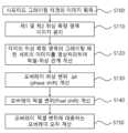
먼저 주어진 시프티드 그레이팅 패턴을 구비한 오버레이 타겟(100)의 이미지를 획득한다(S100). 이미지의 획득은 CCD 카메라와 같은 광학 장비를 사용하는 것이 바람직하나 이에 한정되는 것은 아니다. 예를 들면 CMOS 센서와 같은 다양한 광학 센서를 사용할 수 있다.First, an image of an overlay target (100) having a given shifted grating pattern is acquired (S100). It is preferable to acquire the image using optical equipment such as a CCD camera, but it is not limited thereto. For example, various optical sensors such as a CMOS sensor can be used.
다음으로, 획득된 이미지로부터 제1 및 제2 위상 측정 영역의 이미지를 분리한다(S110). CCD 카메라와 같은 장치로 촬영된 이미지는 컴퓨터 시스템에 설치된 이미지 처리 프로그램에 의해서 처리되어 각각의 시프티드 그레이티 패턴들마다 식별번호가 부여되어 분리될 수 있다.Next, images of the first and second phase measurement areas are separated from the acquired images (S110). Images captured by a device such as a CCD camera are processed by an image processing program installed in a computer system so that each shifted grainy pattern can be separated by assigning an identification number to it.
다음으로, 제1 위상 측정 영역의 각각의 그레이팅 패턴의 이미지를 영상 처리하여 제1 위상 측정 영역의 시프티드 그레이팅 패턴 세트에 대한 픽셀-위상 관계와, 상기 제2 위상 측정 영역의 각각의 그레이팅 패턴의 이미지를 영상 처리하여 제2 위상 측정 영역의 시프티드 그레이팅 패턴 세트에 대한 픽셀-위상 관계를 구한다(S120). 픽셀-위상 관계는 [수학식 1] 및 [수학식 2]를 이용하여 구할 수 있다. 상기의 수학식들을 이용하여 픽셀-위상 관계를 구하는 것은 오버레이 분야의 이미지 처리를 하는 사람에게는 알려진 기술이다.Next, the image of each grating pattern of the first phase measurement area is image-processed to obtain a pixel-phase relationship for a set of shifted grating patterns of the first phase measurement area, and the image of each grating pattern of the second phase measurement area is image-processed to obtain a pixel-phase relationship for a set of shifted grating patterns of the second phase measurement area (S120). The pixel-phase relationship can be obtained using [Mathematical Formula 1] and [Mathematical Formula 2]. Obtaining the pixel-phase relationship using the above mathematical formulas is a technique known to those who perform image processing in the overlay field.
상기 제1 위상 측정 영역의 시프티드 그레이팅 패턴 세트에 대한 픽셀-위상 관계와 제2 위상 측정 영역의 시프티드 그레이팅 패턴 세트에 대한 픽셀-위상 관계를 비교하여 오버레이 위상 변위(Δθ)를 구한다(S130). 오버레이 위상 변위는. 도 4의 그래프에 도시된 것과 같이, 제1 위상 측정 영역의 시프티드 그레이팅 패턴들에 대한 픽셀-위상 관계와 제2 위상 측정 영역의 시프티드 그레이팅 패턴들에 대한 픽셀-위상 관계를 각각 선형 방정식으로 근사하고, 정해진 픽셀에 대응하는 위상값의 차를 구하여 구할 수 있다.The pixel-phase relationship for the set of shifted grating patterns of the first phase measurement area and the pixel-phase relationship for the set of shifted grating patterns of the second phase measurement area are compared to obtain the overlay phase shift (Δθ) (S130). The overlay phase shift can be obtained by approximating the pixel-phase relationship for the shifted grating patterns of the first phase measurement area and the pixel-phase relationship for the shifted grating patterns of the second phase measurement area as linear equations, as shown in the graph of Fig. 4, and obtaining the difference in phase values corresponding to a given pixel.
다음으로, 오버레이 위상 변위(Δθ)에 대응하는 오버레이 픽셀 변위(PS, pixel shift)를 구한다(S140). 오버레이 픽셀 변위는 [수학식 3]를 이용하여 구할 수 있다. 구체적으로 상기 픽셀-위상 관계를 근사한 선형 방정식의 기울기의 역수에 오버레이 위상 변위(Δθ)를 곱하여 오버레이 픽셀 변위를 구한다.Next, the overlay pixel displacement (PS, pixel shift) corresponding to the overlay phase displacement (Δθ) is obtained (S140). The overlay pixel displacement can be obtained using [Mathematical Formula 3]. Specifically, the overlay pixel displacement is obtained by multiplying the inverse of the slope of the linear equation approximating the pixel-phase relationship by the overlay phase displacement (Δθ).
다음으로, 오버레이 픽셀 변위에 대응하는 패턴층들 사이의 실제 오버레이 값을 구한다(S150). 오베레이 픽셀 변위에 대응하는 패턴층들 사이의 실제 오버레이 값은 카메라의 픽셀의 크기에 대응하는 실제 패턴층의 크기의 비율로 광학계의 확대율을 반영하여 구할 수 있다.Next, the actual overlay value between the pattern layers corresponding to the overlay pixel displacement is obtained (S150). The actual overlay value between the pattern layers corresponding to the overlay pixel displacement can be obtained by reflecting the magnification of the optical system as a ratio of the size of the actual pattern layer corresponding to the size of the pixel of the camera.
이상에서 설명된 실시예는 본 발명의 바람직한 실시예를 설명한 것에 불과하고, 본 발명의 권리범위는 설명된 실시예에 한정되는 것은 아니며, 본 발명의 기술적 사상과 특허청구범위 내에서 이 분야의 당업자에 의하여 다양한 변경, 변형 또는 치환이 가능할 것이며, 그와 같은 실시예들은 본 발명의 범위에 속하는 것으로 이해되어야 한다.The embodiments described above merely describe preferred embodiments of the present invention, and the scope of the present invention is not limited to the described embodiments, and various changes, modifications, or substitutions may be made by those skilled in the art within the technical spirit and scope of the claims of the present invention, and it should be understood that such embodiments fall within the scope of the present invention.
100시프티드 그레이팅 패턴을 구비한 오버레이 타겟의 일 실시예
110제1 위상 측정 영역
112, 114, 116제1 시프티드 그레이팅 세트
120: 제2 위상 측정 영역
122, 124, 126제2 시프티드 그레이팅 세트One embodiment of an overlay target having a 100 shifted grating pattern
110 Phase 1 measurement area
112, 114, 116 1st shifted grating set
120: 2nd phase measurement area
122, 124, 126 2nd shifted grating set
Claims (9)
Translated fromKorean제1 패턴층에 제1 방향을 따라, 주기가 동일하고, 적어도 세 개 이상의 위상 차이를 갖도록 구성된 제1 시프티드 그레이팅 패턴 세트가 형성된 제1 위상 측정 영역과,
제2 패턴층에 상기 제1 방향을 따라, 상기 제1 시프티드 그레이팅 패턴 세트와 대응하는 주기와 위상 차이를 갖도록 구성된 제2 시프티드 그레이팅 패턴 세트가 형성된 제2 위상 측정 영역을 포함하며,
상기 제1 위상 측정 영역과 상기 제2 위상 측정 영역은 서로 겹치지 않는 시프티드 그레이팅 패턴을 구비한 오버레이 타겟.As an overlay target for measuring the overlay between pattern layers formed on a substrate,
A first phase measuring region in which a first shifted grating pattern set is formed along a first direction in a first pattern layer, the first shifted grating pattern set having the same period and at least three phase differences;
A second phase measuring region is formed with a second shifted grating pattern set configured to have a period and phase difference corresponding to the first shifted grating pattern set along the first direction in the second pattern layer,
An overlay target having a shifted grating pattern in which the first phase measurement area and the second phase measurement area do not overlap each other.
제1 패턴층에 제2 방향을 따라, 주기가 동일하고, 적어도 세 개 이상의 위상 차이를 갖도록 구성된 제3 시프티드 그레이팅 패턴 세트가 형성된 제3 위상 측정 영역과,
제2 패턴층에 상기 제2 방향을 따라, 상기 제3 시프티드 그레이팅 패턴 세트와 대응하는 주기와 위상 차이를 갖도록 구성된 제4 시프티드 그레이팅 패턴 세트가 형성된 제4 위상 측정 영역을 더 포함하는 시프티드 그레이팅 패턴을 구비한 오버레이 타겟.In the first paragraph,
A third phase measuring region formed with a third shifted grating pattern set configured to have the same period and at least three phase differences along the second direction in the first pattern layer,
An overlay target having a shifted grating pattern further comprising a fourth phase measuring region, in which a fourth set of shifted grating patterns is formed along the second direction in the second pattern layer, the fourth set of shifted grating patterns having a corresponding period and phase difference with the third set of shifted grating patterns.
상기 각각의 시프티드 그레이팅 패턴 세트를 구성하는 그레이팅 패턴들은 상기 제1 방향을 따라 일정한 간격으로 배열된 복수의 직사각형 구조물로 구성된 시프티드 그레이팅 패턴을 구비한 오버레이 타겟.In paragraph 1 or 2,
An overlay target having a shifted grating pattern, wherein the grating patterns constituting each of the above shifted grating pattern sets are composed of a plurality of rectangular structures arranged at regular intervals along the first direction.
제1 시프티드 그레이팅 패턴 세트와 제2 시프티드 그레이팅 패턴 세트는 각각 세 개의 그레이팅 패턴으로 구성되고, 각각의 그레이팅 패턴들은 2/3 π의 위상차를 갖도록 제1 방향으로 따라 시프트 되어 배열된 시프티드 그레이팅 패턴을 구비한 오버레이 타겟.In the third paragraph,
An overlay target having shifted grating patterns, wherein each of the first shifted grating pattern set and the second shifted grating pattern set comprises three grating patterns, and each of the grating patterns is arranged to be shifted along the first direction so as to have a phase difference of 2/3π.
제1 시프티드 그레이팅 패턴 세트와 제2 시프티드 그레이팅 패턴 세트는 각각 네 개의 그레이팅 패턴으로 구성되고, 각각의 그레이팅 패턴들은 1/2 π의 위상차를 갖도록 제1 방향을 따라 시프트 되어 배열된 시프티드 그레이팅 패턴을 구비한 오버레이 타겟.In the third paragraph,
An overlay target having a first shifted grating pattern set and a second shifted grating pattern set, each of which is composed of four grating patterns, and each of the grating patterns having shifted grating patterns arranged along a first direction so as to have a phase difference of 1/2 π.
제2 패턴층에 상기 제1 방향을 따라, 상기 제1 시프티드 그레이팅 패턴 세트와 대응하는 주기와 위상 차이를 갖도록 구성된 제2 시프티드 그레이팅 패턴 세트가 형성된 제2 위상 측정 영역을 포함하며,
상기 제1 위상 측정 영역과 상기 제2 위상 측정 영역은 서로 겹치지 않는 시프티드 그레이팅 패턴을 구비한 오버레이 타겟의 오버레이를 측정하는 방법으로,
상기 시프티드 그레이팅 패턴을 구비한 오버레이 타겟의 이미지를 획득하는 단계와,
상기 획득된 이미지로부터 제1 및 제2 위상 측정 영역의 이미지를 분리하는 단계와,
상기 제1 위상 측정 영역의 각각의 그레이팅 패턴의 이미지를 영상 처리하여 제1 위상 측정 영역의 시프티드 그레이팅 패턴 세트에 대한 픽셀-위상 관계와, 상기 제2 위상 측정 영역의 각각의 그레이팅 패턴의 이미지를 영상 처리하여 제2 위상 측정 영역의 시프티드 그레이팅 패턴 세트에 대한 픽셀-위상 관계를 구하는 단계와,
상기 제1 위상 측정 영역의 시프티드 그레이팅 패턴 세트에 대한 픽셀-위상 관계와 제2 위상 측정 영역의 시프티드 그레이팅 패턴 세트에 대한 픽셀-위상 관계를 비교하여 오버레이 위상 변위(Δθ)를 구하는 단계와,
상기 픽셀-위상 관계를 이용하여 오버레이 위상 변위(Δθ)에 대응하는 오버레이 픽셀 변위를 구하는 단계를 포함하는 시프티드 그레이팅 패턴을 구비한 오버레이 타겟의 오버레이를 측정하는 방법.A first phase measuring region in which a first shifted grating pattern set is formed along a first direction in a first pattern layer, the first shifted grating pattern set having the same period and at least three phase differences;
A second phase measuring region is formed with a second shifted grating pattern set configured to have a period and phase difference corresponding to the first shifted grating pattern set along the first direction in the second pattern layer,
The first phase measurement area and the second phase measurement area are a method for measuring an overlay of an overlay target having a shifted grating pattern that does not overlap each other,
A step of obtaining an image of an overlay target having the above shifted grating pattern,
A step of separating images of the first and second phase measurement areas from the acquired images,
A step of image-processing the image of each grating pattern of the first phase measurement area to obtain a pixel-phase relationship for a set of shifted grating patterns of the first phase measurement area, and a step of image-processing the image of each grating pattern of the second phase measurement area to obtain a pixel-phase relationship for a set of shifted grating patterns of the second phase measurement area,
A step of obtaining an overlay phase shift (Δθ) by comparing the pixel-phase relationship for the shifted grating pattern set of the first phase measurement area with the pixel-phase relationship for the shifted grating pattern set of the second phase measurement area,
A method for measuring an overlay of an overlay target having a shifted grating pattern, comprising the step of obtaining an overlay pixel displacement corresponding to an overlay phase displacement (Δθ) using the above pixel-phase relationship.
상기 오버레이 위상 변위를 구하는 단계는,
제1 위상 측정 영역의 시프티드 그레이팅 패턴 세트에 대한 픽셀-위상 관계와 제2위상 측정 영역의 시프티드 그레이팅 패턴 세트에 대한 픽셀-위상 관계를 각각 선형 방정식으로 근사하고 정해진 픽셀에 대응하는 위상값의 차를 계산하는 단계를 포함하는 시프티드 그레이팅 패턴을 구비한 오버레이 타겟의 오버레이를 측정하는 방법.In Article 6,
The steps for obtaining the above overlay phase shift are:
A method for measuring an overlay of an overlay target having a shifted grating pattern, the method comprising the step of approximating a pixel-phase relationship for a set of shifted grating patterns in a first phase measurement area and a pixel-phase relationship for a set of shifted grating patterns in a second phase measurement area by linear equations, and calculating a difference in phase value corresponding to a given pixel.
상기 오버레이 픽셀 변위를 구하는 단계는,
상기 픽셀-위상 관계를 근사한 선형 방정식의 기울기의 역수에 오버레이 위상 변위(Δθ)를 곱하여 오버레이 픽셀 변위를 구하도록 구성된 시프티드 그레이팅 패턴을 구비한 오버레이 타겟의 오버레이를 측정하는 방법.In Article 7,
The step of calculating the above overlay pixel displacement is:
A method for measuring an overlay of an overlay target having a shifted grating pattern configured to obtain an overlay pixel displacement by multiplying the inverse of the slope of a linear equation approximating the above pixel-phase relationship by the overlay phase shift (Δθ).
제2 패턴층에 상기 제1 방향을 따라, 상기 제1 시프티드 그레이팅 패턴 세트와 대응하는 주기와 위상 차이를 갖도록 구성된 제2 시프티드 그레이팅 패턴 세트가 형성된 제2 위상 측정 영역을 포함하며,
상기 제1 위상 측정 영역과 상기 제2 위상 측정 영역은 서로 겹치지 않는 시프티드 그레이팅 패턴을 구비한 오버레이 타겟의 오버레이를 측정하는 장치로서,
상기 오버레이 타겟을 촬영하기 위한 카메라, 촬영된 이미지를 처리하기 위한 컴퓨터 시스템을 포함하며,
상기 컴퓨터 시스템은, 설치된 프로그램을 통해서,
상기 시프티드 그레이팅 패턴을 구비한 오버레이 타겟의 이미지를 획득하는 단계와,
상기 획득된 이미지로부터 제1 및 제2 위상 측정 영역의 이미지를 분리하는 단계와,
상기 제1 위상 측정 영역의 각각의 그레이팅 패턴의 이미지를 영상 처리하여 제1 위상 측정 영역의 시프티드 그레이팅 패턴 세트에 대한 픽셀-위상 관계와, 상기 제2 위상 측정 영역의 각각의 그레이팅 패턴의 이미지를 영상 처리하여 제2 위상 측정 영역의 시프티드 그레이팅 패턴 세트에 대한 픽셀-위상 관계를 구하는 단계와,
상기 제1 위상 측정 영역의 시프티드 그레이팅 패턴 세트에 대한 픽셀-위상 관계와 제2 위상 측정 영역의 시프티드 그레이팅 패턴 세트에 대한 픽셀-위상 관계를 비교하여 오버레이 위상 변위(Δθ)를 구하는 단계와,
상기 픽셀-위상 관계를 이용하여 오버레이 위상 변위(Δθ)에 대응하는 오버레이 픽셀 변위를 구하는 단계를 수행하는 시프티드 그레이팅 패턴을 구비한 오버레이 타겟의 오버레이를 측정하는 장치.A first phase measuring region in which a first shifted grating pattern set is formed along a first direction in a first pattern layer, the first shifted grating pattern set having the same period and at least three phase differences;
A second phase measuring region is formed with a second shifted grating pattern set configured to have a period and phase difference corresponding to the first shifted grating pattern set along the first direction in the second pattern layer,
The above first phase measurement area and the above second phase measurement area are a device for measuring the overlay of an overlay target having a shifted grating pattern that does not overlap each other,
It includes a camera for photographing the above overlay target and a computer system for processing the photographed image.
The above computer system, through the installed program,
A step of obtaining an image of an overlay target having the above shifted grating pattern,
A step of separating images of the first and second phase measurement areas from the acquired images,
A step of image-processing the image of each grating pattern of the first phase measurement area to obtain a pixel-phase relationship for a set of shifted grating patterns of the first phase measurement area, and a step of image-processing the image of each grating pattern of the second phase measurement area to obtain a pixel-phase relationship for a set of shifted grating patterns of the second phase measurement area,
A step of obtaining an overlay phase shift (Δθ) by comparing the pixel-phase relationship for the shifted grating pattern set of the first phase measurement area with the pixel-phase relationship for the shifted grating pattern set of the second phase measurement area,
A device for measuring an overlay of an overlay target having a shifted grating pattern, the device performing a step of obtaining an overlay pixel displacement corresponding to an overlay phase displacement (Δθ) using the above pixel-phase relationship.
Priority Applications (1)
| Application Number | Priority Date | Filing Date | Title |
|---|---|---|---|
| KR1020210174191AKR102759039B1 (en) | 2021-12-07 | 2021-12-07 | Overlay Target having Shifted Grating Patterns and Method for Measuring the Overlay Error of the Overlay Target |
Applications Claiming Priority (1)
| Application Number | Priority Date | Filing Date | Title |
|---|---|---|---|
| KR1020210174191AKR102759039B1 (en) | 2021-12-07 | 2021-12-07 | Overlay Target having Shifted Grating Patterns and Method for Measuring the Overlay Error of the Overlay Target |
Publications (2)
| Publication Number | Publication Date |
|---|---|
| KR20230085736A KR20230085736A (en) | 2023-06-14 |
| KR102759039B1true KR102759039B1 (en) | 2025-01-23 |
Family
ID=86744722
Family Applications (1)
| Application Number | Title | Priority Date | Filing Date |
|---|---|---|---|
| KR1020210174191AActiveKR102759039B1 (en) | 2021-12-07 | 2021-12-07 | Overlay Target having Shifted Grating Patterns and Method for Measuring the Overlay Error of the Overlay Target |
Country Status (1)
| Country | Link |
|---|---|
| KR (1) | KR102759039B1 (en) |
Family Cites Families (4)
| Publication number | Priority date | Publication date | Assignee | Title |
|---|---|---|---|---|
| US7440105B2 (en)* | 2002-12-05 | 2008-10-21 | Kla-Tencor Technologies Corporation | Continuously varying offset mark and methods of determining overlay |
| US10018919B2 (en)* | 2016-05-29 | 2018-07-10 | Kla-Tencor Corporation | System and method for fabricating metrology targets oriented with an angle rotated with respect to device features |
| KR102221760B1 (en)* | 2016-07-15 | 2021-03-04 | 에이에스엠엘 네델란즈 비.브이. | Apparatus and method for design of metrology target field |
| KR102545173B1 (en)* | 2018-03-09 | 2023-06-19 | 삼성전자주식회사 | A image sensor phase detection pixels and a image pickup device |
- 2021
- 2021-12-07KRKR1020210174191Apatent/KR102759039B1/enactiveActive
Also Published As
| Publication number | Publication date |
|---|---|
| KR20230085736A (en) | 2023-06-14 |
Similar Documents
| Publication | Publication Date | Title |
|---|---|---|
| TWI684074B (en) | Self-referencing and self-calibrating interference pattern overlay measurement | |
| US10107621B2 (en) | Image based overlay measurement with finite gratings | |
| US9719811B2 (en) | Photoelectric encoder including light-receiving element and light-blocking layer that forms light-blocking portion and light-transmitting portion on light-receiving element | |
| EP1851507A2 (en) | Methods and systems for determining overlay error based on target image symmetry | |
| CN110926340A (en) | Novel grating ruler displacement measurement device | |
| KR102804042B1 (en) | Moire Phase Shift Overlay Target and Method for Measuring the Overlay Error of the Overlay Target | |
| JP5854544B1 (en) | Shape measuring apparatus and shape measuring method | |
| US4742233A (en) | Method and apparatus for automated reading of vernier patterns | |
| US11119419B2 (en) | Moiré target and method for using the same in measuring misregistration of semiconductor devices | |
| JPH09229635A (en) | Measuring method of real space length by imaging means, calibration method of optical system, and reference gauge used for calibration of optical system | |
| US7772710B2 (en) | Zero-order overlay targets | |
| KR20240058416A (en) | Overlay Mark for Image Based Overlay Measurement, Overlay Measurement Method, Overlay Measurement Device, and Semiconductor Device Manufacturing Method Using the Same | |
| KR102759039B1 (en) | Overlay Target having Shifted Grating Patterns and Method for Measuring the Overlay Error of the Overlay Target | |
| KR102545517B1 (en) | Overlay Mark Forming a Moire Pattern, Overlay Measurement Method, Overlay Measurement Device, and Semiconductor Device Manufacturing Method Using the Same | |
| CN113330534B (en) | Moiré target and method of use in measuring deflection of a semiconductor device | |
| KR102580204B1 (en) | Overlay Mark for One-dimensional Overlay Measurement, Optical Aberration Evaluation Method, Overlay Mark Quality Evaluation Method, Overlay Measurement Device, Overlay Measurement Method, and Semiconductor Device Manufacturing Method Using the Same | |
| US7697046B2 (en) | Image signal processing device and method of image signal processing including pixel array pattern determination | |
| JPH0135492B2 (en) | ||
| KR102739419B1 (en) | Overlay mark forming moire pattern and overlay measurement method using the same | |
| KR102844370B1 (en) | Overlay Measurement Method and Device Using Upsampling and Semiconductor Device Manufacturing Method Using the Same | |
| KR102823846B1 (en) | Overlay mark forming moire pattern, overlay measurement method and semiconductor device manufacturing method using the same | |
| KR20240150973A (en) | Overlay Mark with a Photonic Crystal Layer, Overlay Measurement Method, Overlay Measurement Device, Semiconductor Device Manufacturing Method Using the Same, and Method for Optimizing a Photonic Crystal Layer | |
| KR102844358B1 (en) | Overlay Mark for Image Based Overlay Measurement, Overlay Measurement Method, Overlay Measurement Device, and Semiconductor Device Manufacturing Method Using the Same | |
| KR20240126587A (en) | Overlay Mark for Image Based Overlay Measurement, Overlay Measurement Method, Overlay Measurement Device, and Semiconductor Device Manufacturing Method Using the Same | |
| KR20250094141A (en) | Overlay Mark with a Reference Pattern, Overlay Measurement Method, Overlay Measurement Device, and Semiconductor Device Manufacturing Method Using the Same |
Legal Events
| Date | Code | Title | Description |
|---|---|---|---|
| PA0109 | Patent application | Patent event code:PA01091R01D Comment text:Patent Application Patent event date:20211207 | |
| PA0201 | Request for examination | ||
| PG1501 | Laying open of application | ||
| E902 | Notification of reason for refusal | ||
| PE0902 | Notice of grounds for rejection | Comment text:Notification of reason for refusal Patent event date:20240223 Patent event code:PE09021S01D | |
| E701 | Decision to grant or registration of patent right | ||
| PE0701 | Decision of registration | Patent event code:PE07011S01D Comment text:Decision to Grant Registration Patent event date:20241121 | |
| GRNT | Written decision to grant | ||
| PR0701 | Registration of establishment | Comment text:Registration of Establishment Patent event date:20250120 Patent event code:PR07011E01D | |
| PR1002 | Payment of registration fee | Payment date:20250120 End annual number:3 Start annual number:1 | |
| PG1601 | Publication of registration |