KR102757508B1 - Semiconductor memory device - Google Patents
Semiconductor memory deviceDownload PDFInfo
- Publication number
- KR102757508B1 KR102757508B1KR1020200098193AKR20200098193AKR102757508B1KR 102757508 B1KR102757508 B1KR 102757508B1KR 1020200098193 AKR1020200098193 AKR 1020200098193AKR 20200098193 AKR20200098193 AKR 20200098193AKR 102757508 B1KR102757508 B1KR 102757508B1
- Authority
- KR
- South Korea
- Prior art keywords
- semiconductor
- semiconductor pattern
- pattern
- memory device
- patterns
- Prior art date
- Legal status (The legal status is an assumption and is not a legal conclusion. Google has not performed a legal analysis and makes no representation as to the accuracy of the status listed.)
- Active
Links
- 239000004065semiconductorSubstances0.000titleclaimsabstractdescription286
- 239000013078crystalSubstances0.000claimsabstractdescription52
- 238000003860storageMethods0.000claimsabstractdescription13
- 230000007547defectEffects0.000claimsdescription22
- 239000010410layerSubstances0.000description160
- 239000000758substrateSubstances0.000description40
- 229910052581Si3N4Inorganic materials0.000description26
- HQVNEWCFYHHQES-UHFFFAOYSA-Nsilicon nitrideChemical compoundN12[Si]34N5[Si]62N3[Si]51N64HQVNEWCFYHHQES-UHFFFAOYSA-N0.000description26
- 238000004519manufacturing processMethods0.000description21
- XUIMIQQOPSSXEZ-UHFFFAOYSA-NSiliconChemical compound[Si]XUIMIQQOPSSXEZ-UHFFFAOYSA-N0.000description17
- 229910052710siliconInorganic materials0.000description17
- 239000010703siliconSubstances0.000description17
- 229910021332silicideInorganic materials0.000description16
- FVBUAEGBCNSCDD-UHFFFAOYSA-Nsilicide(4-)Chemical compound[Si-4]FVBUAEGBCNSCDD-UHFFFAOYSA-N0.000description16
- 238000000034methodMethods0.000description15
- 229910004298SiO 2Inorganic materials0.000description13
- VYPSYNLAJGMNEJ-UHFFFAOYSA-NSilicium dioxideChemical compoundO=[Si]=OVYPSYNLAJGMNEJ-UHFFFAOYSA-N0.000description13
- 229910052814silicon oxideInorganic materials0.000description13
- 239000000463materialSubstances0.000description12
- MRELNEQAGSRDBK-UHFFFAOYSA-Nlanthanum(3+);oxygen(2-)Chemical compound[O-2].[O-2].[O-2].[La+3].[La+3]MRELNEQAGSRDBK-UHFFFAOYSA-N0.000description8
- 229910052732germaniumInorganic materials0.000description7
- GNPVGFCGXDBREM-UHFFFAOYSA-Ngermanium atomChemical compound[Ge]GNPVGFCGXDBREM-UHFFFAOYSA-N0.000description7
- 229910000577Silicon-germaniumInorganic materials0.000description6
- 239000010949copperSubstances0.000description6
- 239000010936titaniumSubstances0.000description6
- 238000005530etchingMethods0.000description5
- 238000005229chemical vapour depositionMethods0.000description4
- 239000010931goldSubstances0.000description4
- 239000012535impuritySubstances0.000description4
- RYGMFSIKBFXOCR-UHFFFAOYSA-NCopperChemical compound[Cu]RYGMFSIKBFXOCR-UHFFFAOYSA-N0.000description3
- RTAQQCXQSZGOHL-UHFFFAOYSA-NTitaniumChemical compound[Ti]RTAQQCXQSZGOHL-UHFFFAOYSA-N0.000description3
- NRTOMJZYCJJWKI-UHFFFAOYSA-NTitanium nitrideChemical compound[Ti]#NNRTOMJZYCJJWKI-UHFFFAOYSA-N0.000description3
- LEVVHYCKPQWKOP-UHFFFAOYSA-N[Si].[Ge]Chemical compound[Si].[Ge]LEVVHYCKPQWKOP-UHFFFAOYSA-N0.000description3
- 229910052782aluminiumInorganic materials0.000description3
- XAGFODPZIPBFFR-UHFFFAOYSA-NaluminiumChemical compound[Al]XAGFODPZIPBFFR-UHFFFAOYSA-N0.000description3
- 238000003491arrayMethods0.000description3
- 229910052802copperInorganic materials0.000description3
- 238000013500data storageMethods0.000description3
- 230000010354integrationEffects0.000description3
- 230000000149penetrating effectEffects0.000description3
- 229910052715tantalumInorganic materials0.000description3
- GUVRBAGPIYLISA-UHFFFAOYSA-Ntantalum atomChemical compound[Ta]GUVRBAGPIYLISA-UHFFFAOYSA-N0.000description3
- MZLGASXMSKOWSE-UHFFFAOYSA-Ntantalum nitrideChemical compound[Ta]#NMZLGASXMSKOWSE-UHFFFAOYSA-N0.000description3
- 229910052719titaniumInorganic materials0.000description3
- WFKWXMTUELFFGS-UHFFFAOYSA-NtungstenChemical compound[W]WFKWXMTUELFFGS-UHFFFAOYSA-N0.000description3
- 229910052721tungstenInorganic materials0.000description3
- 239000010937tungstenSubstances0.000description3
- SKJCKYVIQGBWTN-UHFFFAOYSA-N(4-hydroxyphenyl) methanesulfonateChemical compoundCS(=O)(=O)OC1=CC=C(O)C=C1SKJCKYVIQGBWTN-UHFFFAOYSA-N0.000description2
- WUPHOULIZUERAE-UHFFFAOYSA-N3-(oxolan-2-yl)propanoic acidChemical compoundOC(=O)CCC1CCCO1WUPHOULIZUERAE-UHFFFAOYSA-N0.000description2
- 229910015801BaSrTiOInorganic materials0.000description2
- 229910000530Gallium indium arsenideInorganic materials0.000description2
- 229910004129HfSiOInorganic materials0.000description2
- 229910020654PbScTaOInorganic materials0.000description2
- BQCADISMDOOEFD-UHFFFAOYSA-NSilverChemical compound[Ag]BQCADISMDOOEFD-UHFFFAOYSA-N0.000description2
- GWEVSGVZZGPLCZ-UHFFFAOYSA-NTitan oxideChemical compoundO=[Ti]=OGWEVSGVZZGPLCZ-UHFFFAOYSA-N0.000description2
- 229910006501ZrSiOInorganic materials0.000description2
- KXNLCSXBJCPWGL-UHFFFAOYSA-N[Ga].[As].[In]Chemical compound[Ga].[As].[In]KXNLCSXBJCPWGL-UHFFFAOYSA-N0.000description2
- XWCMFHPRATWWFO-UHFFFAOYSA-N[O-2].[Ta+5].[Sc+3].[O-2].[O-2].[O-2]Chemical compound[O-2].[Ta+5].[Sc+3].[O-2].[O-2].[O-2]XWCMFHPRATWWFO-UHFFFAOYSA-N0.000description2
- UGACIEPFGXRWCH-UHFFFAOYSA-N[Si].[Ti]Chemical compound[Si].[Ti]UGACIEPFGXRWCH-UHFFFAOYSA-N0.000description2
- ILCYGSITMBHYNK-UHFFFAOYSA-N[Si]=O.[Hf]Chemical compound[Si]=O.[Hf]ILCYGSITMBHYNK-UHFFFAOYSA-N0.000description2
- VKJLWXGJGDEGSO-UHFFFAOYSA-Nbarium(2+);oxygen(2-);titanium(4+)Chemical compound[O-2].[O-2].[O-2].[Ti+4].[Ba+2]VKJLWXGJGDEGSO-UHFFFAOYSA-N0.000description2
- 229910052980cadmium sulfideInorganic materials0.000description2
- 229910017052cobaltInorganic materials0.000description2
- 239000010941cobaltSubstances0.000description2
- GUTLYIVDDKVIGB-UHFFFAOYSA-Ncobalt atomChemical compound[Co]GUTLYIVDDKVIGB-UHFFFAOYSA-N0.000description2
- 239000004020conductorSubstances0.000description2
- 238000010586diagramMethods0.000description2
- XUCJHNOBJLKZNU-UHFFFAOYSA-Mdilithium;hydroxideChemical compound[Li+].[Li+].[OH-]XUCJHNOBJLKZNU-UHFFFAOYSA-M0.000description2
- PCHJSUWPFVWCPO-UHFFFAOYSA-NgoldChemical compound[Au]PCHJSUWPFVWCPO-UHFFFAOYSA-N0.000description2
- 229910052737goldInorganic materials0.000description2
- CJNBYAVZURUTKZ-UHFFFAOYSA-Nhafnium(iv) oxideChemical compoundO=[Hf]=OCJNBYAVZURUTKZ-UHFFFAOYSA-N0.000description2
- WPYVAWXEWQSOGY-UHFFFAOYSA-Nindium antimonideChemical compound[Sb]#[In]WPYVAWXEWQSOGY-UHFFFAOYSA-N0.000description2
- 239000011810insulating materialSubstances0.000description2
- 239000011229interlayerSubstances0.000description2
- JQJCSZOEVBFDKO-UHFFFAOYSA-Nlead zincChemical compound[Zn].[Pb]JQJCSZOEVBFDKO-UHFFFAOYSA-N0.000description2
- 229910052751metalInorganic materials0.000description2
- 239000002184metalSubstances0.000description2
- TWNQGVIAIRXVLR-UHFFFAOYSA-Noxo(oxoalumanyloxy)alumaneChemical compoundO=[Al]O[Al]=OTWNQGVIAIRXVLR-UHFFFAOYSA-N0.000description2
- BPUBBGLMJRNUCC-UHFFFAOYSA-Noxygen(2-);tantalum(5+)Chemical compound[O-2].[O-2].[O-2].[O-2].[O-2].[Ta+5].[Ta+5]BPUBBGLMJRNUCC-UHFFFAOYSA-N0.000description2
- RVTZCBVAJQQJTK-UHFFFAOYSA-Noxygen(2-);zirconium(4+)Chemical compound[O-2].[O-2].[Zr+4]RVTZCBVAJQQJTK-UHFFFAOYSA-N0.000description2
- WNUPENMBHHEARK-UHFFFAOYSA-Nsilicon tungstenChemical compound[Si].[W]WNUPENMBHHEARK-UHFFFAOYSA-N0.000description2
- 229910052709silverInorganic materials0.000description2
- 239000004332silverSubstances0.000description2
- PWYYWQHXAPXYMF-UHFFFAOYSA-Nstrontium(2+)Chemical compound[Sr+2]PWYYWQHXAPXYMF-UHFFFAOYSA-N0.000description2
- CZXRMHUWVGPWRM-UHFFFAOYSA-Nstrontium;barium(2+);oxygen(2-);titanium(4+)Chemical compound[O-2].[O-2].[O-2].[O-2].[Ti+4].[Sr+2].[Ba+2]CZXRMHUWVGPWRM-UHFFFAOYSA-N0.000description2
- 238000001039wet etchingMethods0.000description2
- 229910001928zirconium oxideInorganic materials0.000description2
- GFQYVLUOOAAOGM-UHFFFAOYSA-Nzirconium(iv) silicateChemical compound[Zr+4].[O-][Si]([O-])([O-])[O-]GFQYVLUOOAAOGM-UHFFFAOYSA-N0.000description2
- JBRZTFJDHDCESZ-UHFFFAOYSA-NAsGaChemical compound[As]#[Ga]JBRZTFJDHDCESZ-UHFFFAOYSA-N0.000description1
- GPXJNWSHGFTCBW-UHFFFAOYSA-NIndium phosphideChemical compound[In]#PGPXJNWSHGFTCBW-UHFFFAOYSA-N0.000description1
- 239000003990capacitorSubstances0.000description1
- 239000003989dielectric materialSubstances0.000description1
- -1for exampleSubstances0.000description1
- HZXMRANICFIONG-UHFFFAOYSA-Ngallium phosphideChemical compound[Ga]#PHZXMRANICFIONG-UHFFFAOYSA-N0.000description1
- RPQDHPTXJYYUPQ-UHFFFAOYSA-Nindium arsenideChemical compound[In]#[As]RPQDHPTXJYYUPQ-UHFFFAOYSA-N0.000description1
- 239000007769metal materialSubstances0.000description1
- 229910021421monocrystalline siliconInorganic materials0.000description1
- 238000000059patterningMethods0.000description1
- 239000012782phase change materialSubstances0.000description1
Images


Classifications
- H—ELECTRICITY
- H10—SEMICONDUCTOR DEVICES; ELECTRIC SOLID-STATE DEVICES NOT OTHERWISE PROVIDED FOR
- H10B—ELECTRONIC MEMORY DEVICES
- H10B41/00—Electrically erasable-and-programmable ROM [EEPROM] devices comprising floating gates
- H10B41/20—Electrically erasable-and-programmable ROM [EEPROM] devices comprising floating gates characterised by three-dimensional arrangements, e.g. with cells on different height levels
- H—ELECTRICITY
- H10—SEMICONDUCTOR DEVICES; ELECTRIC SOLID-STATE DEVICES NOT OTHERWISE PROVIDED FOR
- H10B—ELECTRONIC MEMORY DEVICES
- H10B12/00—Dynamic random access memory [DRAM] devices
- H10B12/01—Manufacture or treatment
- H10B12/02—Manufacture or treatment for one transistor one-capacitor [1T-1C] memory cells
- H10B12/03—Making the capacitor or connections thereto
- H—ELECTRICITY
- H10—SEMICONDUCTOR DEVICES; ELECTRIC SOLID-STATE DEVICES NOT OTHERWISE PROVIDED FOR
- H10B—ELECTRONIC MEMORY DEVICES
- H10B12/00—Dynamic random access memory [DRAM] devices
- H10B12/01—Manufacture or treatment
- H10B12/02—Manufacture or treatment for one transistor one-capacitor [1T-1C] memory cells
- H10B12/05—Making the transistor
- H—ELECTRICITY
- H10—SEMICONDUCTOR DEVICES; ELECTRIC SOLID-STATE DEVICES NOT OTHERWISE PROVIDED FOR
- H10B—ELECTRONIC MEMORY DEVICES
- H10B12/00—Dynamic random access memory [DRAM] devices
- H10B12/30—DRAM devices comprising one-transistor - one-capacitor [1T-1C] memory cells
- H—ELECTRICITY
- H10—SEMICONDUCTOR DEVICES; ELECTRIC SOLID-STATE DEVICES NOT OTHERWISE PROVIDED FOR
- H10B—ELECTRONIC MEMORY DEVICES
- H10B12/00—Dynamic random access memory [DRAM] devices
- H10B12/30—DRAM devices comprising one-transistor - one-capacitor [1T-1C] memory cells
- H10B12/48—Data lines or contacts therefor
- H10B12/482—Bit lines
- H—ELECTRICITY
- H10—SEMICONDUCTOR DEVICES; ELECTRIC SOLID-STATE DEVICES NOT OTHERWISE PROVIDED FOR
- H10B—ELECTRONIC MEMORY DEVICES
- H10B43/00—EEPROM devices comprising charge-trapping gate insulators
- H10B43/20—EEPROM devices comprising charge-trapping gate insulators characterised by three-dimensional arrangements, e.g. with cells on different height levels
- H—ELECTRICITY
- H10—SEMICONDUCTOR DEVICES; ELECTRIC SOLID-STATE DEVICES NOT OTHERWISE PROVIDED FOR
- H10D—INORGANIC ELECTRIC SEMICONDUCTOR DEVICES
- H10D1/00—Resistors, capacitors or inductors
- H10D1/60—Capacitors
- H10D1/68—Capacitors having no potential barriers
- H—ELECTRICITY
- H10—SEMICONDUCTOR DEVICES; ELECTRIC SOLID-STATE DEVICES NOT OTHERWISE PROVIDED FOR
- H10D—INORGANIC ELECTRIC SEMICONDUCTOR DEVICES
- H10D88/00—Three-dimensional [3D] integrated devices
Landscapes
- Engineering & Computer Science (AREA)
- Manufacturing & Machinery (AREA)
- Semiconductor Memories (AREA)
- Non-Volatile Memory (AREA)
- Power Engineering (AREA)
Abstract
Translated fromKoreanDescription
Translated fromKorean본 개시는 반도체 메모리 소자에 관한 것이다. 보다 구체적으로는 3차원 반도체 메모리 소자에 관한 것이다.The present disclosure relates to a semiconductor memory device. More specifically, it relates to a three-dimensional semiconductor memory device.
전자 기기의 고성능화, 고속화, 및 소형화가 지속적으로 요구되고 있다. 따라서 전자 기기에 포함되는 반도체 메모리 소자의 고집적화가 지속적으로 요구되고 있다. 메모리 셀의 평면적을 감소시킴으로써 반도체 메모리 소자의 집적도가 향상될 수 있다. 그러나, 메모리 셀의 평면적의 감소는 공정적 한계에 도달하고 있다. 집적도의 추가적인 향상을 위하여, 메모리 셀을 수직 방향으로 적층하는 3차원 반도체 메모리 소자가 제안되었다.Electronic devices are continuously required to be more high-performance, faster, and smaller. Accordingly, high integration of semiconductor memory devices included in electronic devices is continuously required. The integration of semiconductor memory devices can be improved by reducing the planar area of memory cells. However, the reduction in the planar area of memory cells is reaching the process limit. In order to further improve the integration, a three-dimensional semiconductor memory device in which memory cells are stacked vertically has been proposed.
본 개시가 해결하고자 하는 과제는 제조하기 용이한 3차원 반도체 메모리 소자를 제공하는 것이다.The problem that the present disclosure seeks to solve is to provide a three-dimensional semiconductor memory device that is easy to manufacture.
본 개시의 일 실시예에 따른 반도체 메모리 소자는 수직 방향으로 서로 이격된 제1 반도체 패턴 및 제2 반도체 패턴, 상기 제1 반도체 패턴 및 상기 제2 반도체 패턴의 제1 소스/드레인 영역들에 각각 전기적으로 연결되는 두 비트 라인, 상기 제1 반도체 패턴 및 상기 제2 반도체 패턴과 접촉하는 워드 라인 구조체, 및 상기 제1 반도체 패턴 및 상기 제2 반도체 패턴의 제2 소스/드레인 영역들에 각각 전기적으로 연결되는 두 정보 저장 요소를 포함하고, 상기 제1 반도체 패턴 및 상기 제2 반도체 패턴은 단결정이고, 상기 제1 반도체 패턴의 결정 방향은 상기 제2 반도체 패턴의 결정 방향과 상이할 수 있다.According to one embodiment of the present disclosure, a semiconductor memory device includes a first semiconductor pattern and a second semiconductor pattern which are vertically spaced apart from each other, two bit lines each electrically connected to first source/drain regions of the first semiconductor pattern and the second semiconductor pattern, a word line structure in contact with the first semiconductor pattern and the second semiconductor pattern, and two information storage elements each electrically connected to second source/drain regions of the first semiconductor pattern and the second semiconductor pattern, wherein the first semiconductor pattern and the second semiconductor pattern are single crystals, and a crystal direction of the first semiconductor pattern may be different from a crystal direction of the second semiconductor pattern.
본 개시의 일 실시예에 따른 반도체 메모리 소자는 수직 방향으로 서로 이격된 복수의 반도체 패턴, 상기 복수의 반도체 패턴의 제1 소스/드레인 영역들에 전기적으로 연결되는 비트 라인, 상기 복수의 반도체 패턴 상에 각각 접촉하는 복수의 워드 라인 구조체, 및 상기 복수의 반도체 패턴의 제2 소스/드레인 영역들에 각각 전기적으로 연결되는 복수의 정보 저장 요소를 포함하고, 상기 복수의 반도체 패턴은 단결정이고, 상기 복수의 반도체 패턴 중 적어도 하나의 결정 방향은 상기 복수의 반도체 패턴 중 다른 하나의 결정 방향과 상이할 수 있다.According to one embodiment of the present disclosure, a semiconductor memory device includes a plurality of semiconductor patterns spaced apart from each other in a vertical direction, a bit line electrically connected to first source/drain regions of the plurality of semiconductor patterns, a plurality of word line structures respectively contacting the plurality of semiconductor patterns, and a plurality of information storage elements electrically connected to second source/drain regions of the plurality of semiconductor patterns, wherein the plurality of semiconductor patterns are single crystals, and a crystal direction of at least one of the plurality of semiconductor patterns may be different from a crystal direction of another one of the plurality of semiconductor patterns.
본 개시의 일 실시예에 따른 반도체 메모리 소자는 수직 방향 및 제1 수평 방향으로 2차원적으로 배열되며 각각이 제2 수평 방향으로 연장되는 복수의 반도체 패턴, 상기 복수의 반도체 패턴을 상기 수직 방향으로 이격시키는 복수의 절연 층, 상기 복수의 반도체 패턴 중 몇몇의 제1 소스/드레인 영역들에 전기적으로 연결되는 비트 라인, 상기 복수의 반도체 패턴 중 몇몇과 접촉하는 워드 라인 구조체, 및 상기 복수의 반도체 패턴의 제2 소스/드레인 영역들에 각각 전기적으로 연결되는 복수의 정보 저장 요소를 포함하고, 상기 복수의 반도체 패턴은 단결정이고, 상기 복수의 반도체 패턴 중 적어도 하나의 결정 방향은 상기 복수의 반도체 패턴 중 다른 하나의 결정 방향과 상이할 수 있다.According to one embodiment of the present disclosure, a semiconductor memory device includes a plurality of semiconductor patterns that are two-dimensionally arranged in a vertical direction and a first horizontal direction and each extending in a second horizontal direction, a plurality of insulating layers that space the plurality of semiconductor patterns apart in the vertical direction, a bit line electrically connected to first source/drain regions of some of the plurality of semiconductor patterns, a word line structure in contact with some of the plurality of semiconductor patterns, and a plurality of information storage elements electrically connected to second source/drain regions of the plurality of semiconductor patterns, respectively, wherein the plurality of semiconductor patterns are single crystals, and a crystal direction of at least one of the plurality of semiconductor patterns may be different from a crystal direction of another one of the plurality of semiconductor patterns.
본 개시의 일 실시예에 따른 반도체 메모리 소자 제조 방법에 따르면, 다결정 반도체 시드를 사용하여 단결정 반도체 패턴이 형성될 수 있다. 단결정 반도체 시드가 필요 없으므로 제조 공정의 난이도 및 비용이 감소될 수 있다. 단결정 반도체 패턴이 반도체 메모리 소자에 포함되므로 반도체 메모리 소자의 전기적 특성 및 신뢰성이 향상될 수 있다.According to a method for manufacturing a semiconductor memory device according to one embodiment of the present disclosure, a single-crystal semiconductor pattern can be formed using a polycrystalline semiconductor seed. Since a single-crystal semiconductor seed is not required, the difficulty and cost of a manufacturing process can be reduced. Since a single-crystal semiconductor pattern is included in a semiconductor memory device, the electrical characteristics and reliability of the semiconductor memory device can be improved.
도 1은 본 개시의 일 실시예에 따른 반도체 메모리 소자의 셀 어레이를 나타내는 회로도이다.
도 2는 본 개시의 일 실시예에 따른 반도체 메모리 소자를 나타낸 사시도이다.
도 3은 본 개시의 일 실시예에 따른 반도체 메모리 소자를 나타내는 사시도이다.
도 4a 내지 도 4c는 각각 도 3의 A-A' 선, B-B' 선, 및 C-C' 선에 따른 단면도들이다.
도 5a 내지 도 5f는 본 개시의 일 실시예에 따른 반도체 메모리 소자를 제조하기 위한 적층 구조체를 제조하는 방법들을 설명하기 위한 단면도들이다.
도 6a 내지 도 6e는 본 개시의 일 실시예에 따른 반도체 메모리 소자를 제조하기 위한 적층 구조체를 제조하는 방법들을 설명하기 위한 단면도들이다.
도 7a 내지 도 7g는 본 개시의 일 실시예에 따른 반도체 메모리 소자를 제조하기 위한 적층 구조체를 제조하는 방법들을 설명하기 위한 단면도들이다.
도 8a, 도 9a, 도 10a, 도 11a, 도 12a, 도 13a, 및 도 14a는 도 5a 내지 도 5f, 도 6a 내지 도 6e, 또는 도 7a 내지 도 7g에 따라 제조된 적층 구조체를 사용하여 본 개시의 일 실시예에 따른 반도체 메모리 소자를 제조하는 방법을 설명하기 위한 평면 단면도들이다.
도 8b, 도 9b, 도 10b, 도 11b, 도 12b, 도 13b, 및 도 14b는 각각 도 8a, 도 9a, 도 10a, 도 11a, 도 12a, 도 13a, 및 도 14a의 A-A' 선을 따른 단면도들이다.
도 8c, 도 9c, 도 10c, 도 11c, 도 12c, 도 13c, 및 도 14c는 각각 도 8a, 도 9a, 도 10a, 도 11a, 도 12a, 도 13a, 및 도 14a의 B-B' 선을 따른 단면도들이다.
도 15는 본 개시의 일 실시예에 따른 반도체 메모리 소자를 나타낸 사시도이다.
도 16a는 본 개시의 일 실시예에 따른 반도체 메모리 소자를 나타낸 평면도이다.
도 16b는 도 16a의 A-A' 선을 따른 단면도이다.FIG. 1 is a circuit diagram showing a cell array of a semiconductor memory device according to one embodiment of the present disclosure.
FIG. 2 is a perspective view illustrating a semiconductor memory device according to one embodiment of the present disclosure.
FIG. 3 is a perspective view showing a semiconductor memory device according to one embodiment of the present disclosure.
Figures 4a to 4c are cross-sectional views taken along lines AA', BB', and CC' of Figure 3, respectively.
FIGS. 5A to 5F are cross-sectional views illustrating methods for manufacturing a laminated structure for manufacturing a semiconductor memory device according to one embodiment of the present disclosure.
FIGS. 6A to 6E are cross-sectional views illustrating methods for manufacturing a laminated structure for manufacturing a semiconductor memory device according to one embodiment of the present disclosure.
FIGS. 7A to 7G are cross-sectional views illustrating methods for manufacturing a laminated structure for manufacturing a semiconductor memory device according to one embodiment of the present disclosure.
FIGS. 8A, 9A, 10A, 11A, 12A, 13A, and 14A are cross-sectional plan views illustrating a method of manufacturing a semiconductor memory device according to one embodiment of the present disclosure using a laminated structure manufactured according to FIGS. 5A to 5F, 6A to 6E, or 7A to 7G.
FIGS. 8b, 9b, 10b, 11b, 12b, 13b, and 14b are cross-sectional views taken along line AA' of FIGS. 8a, 9a, 10a, 11a, 12a, 13a, and 14a, respectively.
FIGS. 8c, 9c, 10c, 11c, 12c, 13c, and 14c are cross-sectional views taken along line BB' of FIGS. 8a, 9a, 10a, 11a, 12a, 13a, and 14a, respectively.
FIG. 15 is a perspective view showing a semiconductor memory device according to one embodiment of the present disclosure.
FIG. 16a is a plan view illustrating a semiconductor memory device according to one embodiment of the present disclosure.
Figure 16b is a cross-sectional view along line AA' of Figure 16a.
도 1은 본 개시의 일 실시예에 따른 반도체 메모리 소자의 셀 어레이를 나타내는 회로도이다.FIG. 1 is a circuit diagram showing a cell array of a semiconductor memory device according to one embodiment of the present disclosure.
도 1을 참조하면, 본 개시의 일 실시예에 따른 반도체 메모리 소자의 셀 어레이는 복수의 서브 셀 어레이(SCA)를 포함할 수 있다. 복수의 서브 셀 어레이(SCA)는 제2 수평 방향(D2)을 따라 배열될 수 있다. 각각의 서브 셀 어레이(SCA)는 복수의 비트 라인(BL), 복수의 워드 라인(WL), 복수의 메모리 셀 트랜지스터(MCT), 및 복수의 정보 저장 요소(DS)를 포함할 수 있다.Referring to FIG. 1, a cell array of a semiconductor memory device according to an embodiment of the present disclosure may include a plurality of sub-cell arrays (SCAs). The plurality of sub-cell arrays (SCAs) may be arranged along a second horizontal direction (D2). Each sub-cell array (SCA) may include a plurality of bit lines (BLs), a plurality of word lines (WLs), a plurality of memory cell transistors (MCTs), and a plurality of information storage elements (DS).
각각의 비트 라인(BL)은 제1 수평 방향(D1)으로 연장되며 하나의 서브 셀 어레이(SCA) 내의 복수의 비트 라인(BL)은 수직 방향(D3)으로 서로 이격될 수 있다. 하나의 비트 라인(BL)은 제1 수평 방향(D1)을 따라 배열된 복수의 메모리 셀 트랜지스터(MCT)의 제1 소스/드레인 영역에 전기적으로 연결될 수 있다.Each bit line (BL) extends in a first horizontal direction (D1), and a plurality of bit lines (BLs) within one sub-cell array (SCA) can be spaced apart from each other in a vertical direction (D3). One bit line (BL) can be electrically connected to a first source/drain region of a plurality of memory cell transistors (MCTs) arranged along the first horizontal direction (D1).
각각의 워드 라인(WL)은 수직 방향(D3)으로 연장되며 하나의 서브 셀 어레이(SCA) 내의 복수의 워드 라인(WL)은 제1 수평 방향(D1)으로 서로 이격될 수 있다. 하나의 워드 라인(WL)은 수직 방향(D3)을 따라 배열된 복수의 메모리 셀 트랜지스터(MCT)의 게이트에 전기적으로 연결될 수 있다.Each word line (WL) extends in the vertical direction (D3), and a plurality of word lines (WL) within one sub-cell array (SCA) can be spaced apart from each other in the first horizontal direction (D1). One word line (WL) can be electrically connected to gates of a plurality of memory cell transistors (MCT) arranged along the vertical direction (D3).
하나의 서브 셀 어레이(SCA) 내의 복수의 메모리 셀 트랜지스터(MCT)는 제1 수평 방향(D1) 및 수직 방향(D3)으로 배열될 수 있다. 정보 저장 요소(DS)는 각각의 메모리 셀 트랜지스터(MCT)의 제2 소스/드레인 영역에 전기적으로 연결될 수 있다. 정보 저장 요소(DS)는 예를 들어 자기터널접합, 상 변화 물질, 또는 캐패시터를 포함할 수 있다.A plurality of memory cell transistors (MCTs) within a single sub-cell array (SCA) may be arranged in a first horizontal direction (D1) and a vertical direction (D3). A data storage element (DS) may be electrically connected to a second source/drain region of each memory cell transistor (MCT). The data storage element (DS) may include, for example, a magnetic tunnel junction, a phase change material, or a capacitor.
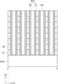
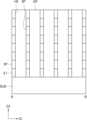
도 2는 본 개시의 일 실시예에 따른 반도체 메모리 소자를 나타낸 사시도이다.FIG. 2 is a perspective view illustrating a semiconductor memory device according to one embodiment of the present disclosure.
도 1 및 도 2를 참조하면, 도 1을 참조하여 설명한 복수의 서브 셀 어레이(SCA) 중 하나가 기판(SUB) 상에 배치될 수 있다. 기판(SUB)은 반도체 물질, 예를 들어 Ⅳ족 반도체 물질, Ⅲ-Ⅴ족 반도체 물질, Ⅱ-Ⅵ족 반도체 물질, 또는 이들의 조합을 포함할 수 있다. 상기 Ⅳ족 반도체 물질은 예를 들어 실리콘(Si), 또는 게르마늄(Ge)을 포함할 수 있다. 상기 Ⅲ-Ⅴ족 반도체 물질은 예를 들어 갈륨비소(GaAs), 인듐인(InP), 갈륨인(GaP), 인듐비소(InAs), 인듐 안티몬(InSb), 또는 인듐갈륨비소(InGaAs)를 포함할 수 있다. 상기 Ⅱ-Ⅵ족 반도체 물질은 예를 들어 텔루르화 아연(ZnTe), 또는 황화카드뮴(CdS)을 포함할 수 있다.Referring to FIGS. 1 and 2, one of the plurality of sub-cell arrays (SCA) described with reference to FIG. 1 may be disposed on a substrate (SUB). The substrate (SUB) may include a semiconductor material, for example, a group IV semiconductor material, a group III-V semiconductor material, a group II-VI semiconductor material, or a combination thereof. The group IV semiconductor material may include, for example, silicon (Si) or germanium (Ge). The group III-V semiconductor material may include, for example, gallium arsenide (GaAs), indium phosphide (InP), gallium phosphide (GaP), indium arsenide (InAs), indium antimony (InSb), or indium gallium arsenide (InGaAs). The group II-VI semiconductor material may include, for example, zinc telluride (ZnTe) or cadmium sulfide (CdS).
각각의 서브 셀 어레이(SCA, 도 1 참조)는 복수의 비트 라인(BL), 복수의 워드 라인 구조체(WLS), 복수의 반도체 패턴(SP), 및 복수의 정보 저장 요소(DS)를 포함할 수 있다. 반도체 패턴(SP) 및 워드 라인 구조체(WLS)는 도 1의 메모리 셀 트랜지스터(MCT)에 대응할 수 있다. 워드 라인 구조체(WLS)는 또한 도 1의 워드 라인(WL)에 대응할 수 있다.Each sub-cell array (SCA, see FIG. 1) may include a plurality of bit lines (BLs), a plurality of word line structures (WLS), a plurality of semiconductor patterns (SPs), and a plurality of information storage elements (DSs). The semiconductor patterns (SPs) and the word line structures (WLSs) may correspond to the memory cell transistors (MCTs) of FIG. 1. The word line structures (WLSs) may also correspond to the word lines (WLs) of FIG. 1.
복수의 반도체 패턴(SP)이 제1 수평 방향(D1) 및 수직 방향(D3)으로 서로 이격될 수 있다. 각각의 반도체 패턴(SP)은 제2 수평 방향(D2)으로 연장되는 바(bar) 또는 기둥(pillar)의 형상을 가질 수 있다. 반도체 패턴(SP)은 단결정 반도체 물질. 예를 들어, 단결정 실리콘(Si), 단결정 게르마늄(Ge), 또는 단결정 실리콘-게르마늄(SiGe)을 포함할 수 있다. 복수의 반도체 패턴(SP) 중 하나의 결정 방향은 복수의 반도체 패턴(SP) 중 다른 하나의 결정 방향과 상이할 수 있다.A plurality of semiconductor patterns (SP) may be spaced apart from each other in a first horizontal direction (D1) and a vertical direction (D3). Each semiconductor pattern (SP) may have a shape of a bar or a pillar extending in a second horizontal direction (D2). The semiconductor pattern (SP) may include a single crystal semiconductor material. For example, single crystal silicon (Si), single crystal germanium (Ge), or single crystal silicon-germanium (SiGe). A crystal direction of one of the plurality of semiconductor patterns (SP) may be different from a crystal direction of another one of the plurality of semiconductor patterns (SP).
예를 들어, 복수의 반도체 패턴(SP)은 수직 방향(D3)으로 서로 이격된 제1 반도체 패턴(SP1) 및 제2 반도체 패턴(SP2)을 포함할 수 있고, 제1 반도체 패턴(SP1)의 결정 방향은 제2 반도체 패턴(SP2)의 결정 방향과 상이할 수 있다. 복수의 반도체 패턴(SP)은 제3 반도체 패턴(SP3)을 더 포함할 수 있고, 제3 반도체 패턴(SP3)은 제2 반도체 패턴(SP2)으로부터 수직 방향(D3)으로 이격될 수 있다. 제3 반도체 패턴(SP3)의 결정 방향은 제1 반도체 패턴(SP1)의 결정 방향과 동일하거나, 제2 반도체 패턴(SP2)의 결정 방향과 동일하거나, 제1 반도체 패턴(SP1)의 결정 방향 및 제2 반도체 패턴(SP2)의 결정 방향과 상이할 수 있다.For example, the plurality of semiconductor patterns (SP) may include a first semiconductor pattern (SP1) and a second semiconductor pattern (SP2) spaced apart from each other in a vertical direction (D3), and a crystal direction of the first semiconductor pattern (SP1) may be different from a crystal direction of the second semiconductor pattern (SP2). The plurality of semiconductor patterns (SP) may further include a third semiconductor pattern (SP3), and the third semiconductor pattern (SP3) may be spaced apart from the second semiconductor pattern (SP2) in the vertical direction (D3). The crystal direction of the third semiconductor pattern (SP3) may be the same as the crystal direction of the first semiconductor pattern (SP1), the same as the crystal direction of the second semiconductor pattern (SP2), or different from the crystal direction of the first semiconductor pattern (SP1) and the crystal direction of the second semiconductor pattern (SP2).
각각의 반도체 패턴(SP)은 채널 영역(CH) 및 채널 영역(CH)의 양 단의 제1 소스/드레인 영역(SD1) 및 제2 소스/드레인 영역(SD2)을 포함할 수 있다. 즉, 제1 소스/드레인 영역(SD1) 및 제2 소스/드레인 영역(SD2)은 제2 수평 방향(D2)으로 서로 이격될 수 있다. 제1 및 제2 소스/드레인 영역(SD1, SD2) 각각은 n형 또는 p형 불순물로 도핑될 수 있다. 각각의 반도체 패턴(SP)의 제2 소스/드레인 영역(SD2)은 정보 저장 요소(DS)에 연결될 수 있다.Each semiconductor pattern (SP) may include a channel region (CH) and a first source/drain region (SD1) and a second source/drain region (SD2) at opposite ends of the channel region (CH). That is, the first source/drain region (SD1) and the second source/drain region (SD2) may be spaced apart from each other in a second horizontal direction (D2). Each of the first and second source/drain regions (SD1, SD2) may be doped with an n-type or p-type impurity. The second source/drain region (SD2) of each semiconductor pattern (SP) may be connected to a data storage element (DS).
각각의 비트 라인(BL)은 제1 수평 방향(D1)으로 연장될 수 있고, 복수의 비트 라인(BL)은 수직 방향(D3)으로 서로 이격될 수 있다. 제1 수평 방향(D1)으로 이격된 복수의 반도체 패턴(SP)의 제1 소스/드레인 영역(SD1)은 동일한 비트 라인(BL)에 전기적으로 연결될 수 있다. 수직 방향(D3)으로 이격된 복수의 반도체 패턴(SP)의 제1 소스/드레인 영역(SD1)은 상이한 복수의 비트 라인(BL)에 각각 전기적으로 연결될 수 있다. 비트 라인(BL)은 도전 물질, 예를 들어, 도핑된 실리콘(doped Si), 도핑된 게르마늄(doped Ge), 질화 티타늄(TiN), 질화 탄탈륨(TaN), 텅스텐(W), 티타늄(Ti), 탄탈륨(Ta), 구리(Cu), 알루미늄(Al), 은(Ag), 금(Au), 텅스텐 실리사이드(WSi), 코발트 실리사이드(CoSi), 티타늄 실리사이드(TiSi), 또는 이들의 조합을 포함할 수 있다.Each bit line (BL) can extend in a first horizontal direction (D1), and a plurality of bit lines (BL) can be spaced apart from each other in a vertical direction (D3). First source/drain regions (SD1) of a plurality of semiconductor patterns (SP) spaced apart in the first horizontal direction (D1) can be electrically connected to the same bit line (BL). First source/drain regions (SD1) of a plurality of semiconductor patterns (SP) spaced apart in the vertical direction (D3) can be electrically connected to different bit lines (BL), respectively. The bit line (BL) may include a conductive material, such as doped silicon (doped Si), doped germanium (doped Ge), titanium nitride (TiN), tantalum nitride (TaN), tungsten (W), titanium (Ti), tantalum (Ta), copper (Cu), aluminum (Al), silver (Ag), gold (Au), tungsten silicide (WSi), cobalt silicide (CoSi), titanium silicide (TiSi), or a combination thereof.
각각의 워드 라인 구조체(WLS)는 수직 방향(D3)으로 연장될 수 있고, 복수의 워드 라인 구조체(WLS)는 제1 수평 방향(D1)으로 서로 이격될 수 있다. 수직 방향(D3)으로 이격된 복수의 반도체 패턴(SP)은 동일한 워드 라인 구조체(WLS)에 접촉할 수 있다. 워드 라인 구조체(WLS)는 수직 방향(D3)으로 이격된 복수의 반도체 패턴(SP)의 양 측면과 접촉할 수 있다. 예를 들어, 워드 라인 구조체(WLS)는 제1 내지 제3 반도체 패턴(SP1 내지 SP3)의 양 측면과 접촉할 수 있다. 제1 수평 방향(D3)으로 서로 이격된 복수의 반도체 패턴(SP)은 상이한 복수의 워드 라인 구조체(WLS)에 각각 접촉할 수 있다.Each word line structure (WLS) can extend in the vertical direction (D3), and a plurality of word line structures (WLS) can be spaced apart from each other in a first horizontal direction (D1). A plurality of semiconductor patterns (SP) spaced apart in the vertical direction (D3) can contact the same word line structure (WLS). The word line structure (WLS) can contact both side surfaces of the plurality of semiconductor patterns (SP) spaced apart in the vertical direction (D3). For example, the word line structure (WLS) can contact both side surfaces of the first to third semiconductor patterns (SP1 to SP3). A plurality of semiconductor patterns (SP) spaced apart from each other in the first horizontal direction (D3) can each contact different word line structures (WLS).
워드 라인 구조체(WLS)는 게이트 전극(GE) 및 게이트 전극(GE)과 채널 영역(CH) 사이의 게이트 절연 층(GI)을 포함할 수 있다. 게이트 전극(GE)은 도전 물질, 예를 들어, 도핑된 실리콘(doped Si), 도핑된 게르마늄(doped Ge), 질화 티타늄(TiN), 질화 탄탈륨(TaN), 텅스텐(W), 티타늄(Ti), 탄탈륨(Ta), 구리(Cu), 알루미늄(Al), 은(Ag), 금(Au), 텅스텐 실리사이드(WSi), 코발트 실리사이드(CoSi), 티타늄 실리사이드(TiSi), 또는 이들의 조합을 포함할 수 있다. 게이트 절연 층(GI)은 고유전 물질, 실리콘 산화물(SiO2), 실리콘 질화물(SiN), 실리콘 산질화물(SiON), 또는 이들의 조합을 포함할 수 있다. 상기 고유전 물질은 하프늄 산화물(HfO2), 하프늄 실리콘 산화물(HfSiO2), 란탄 산화물(LaO), 지르코늄산화물(ZrO2), 지르코늄 실리콘 산화물(ZrSiO2), 탄탈륨 산화물(Ta2O5), 티타늄 산화물(TiO2), 바륨 스트론튬 티타늄 산화물(BaSrTiO3), 바륨 티타늄 산화물(BaTiO3), 스트론튬 티타늄 산화물(SrTiO3), 리튬 산화물(Li2O), 알루미늄 산화물(Al2O-3), 납 스칸듐 탄탈륨 산화물(PbScTaO), 납 아연 니오브산염(PbZnNbO3), 또는 이들의 조합을 포함할 수 있다.The word line structure (WLS) may include a gate electrode (GE) and a gate insulating layer (GI) between the gate electrode (GE) and a channel region (CH). The gate electrode (GE) may include a conductive material, such as doped silicon (doped Si), doped germanium (doped Ge), titanium nitride (TiN), tantalum nitride (TaN), tungsten (W), titanium (Ti), tantalum (Ta), copper (Cu), aluminum (Al), silver (Ag), gold (Au), tungsten silicide (WSi), cobalt silicide (CoSi), titanium silicide (TiSi), or a combination thereof. The gate insulating layer (GI) may include a high-k material, such as silicon oxide (SiO2 ), silicon nitride (SiN), silicon oxynitride (SiON), or a combination thereof. The above high-dielectric material may include hafnium oxide (HfO2 ), hafnium silicon oxide (HfSiO2 ), lanthanum oxide (LaO), zirconium oxide (ZrO2 ), zirconium silicon oxide (ZrSiO2 ), tantalum oxide (Ta2 O5 ), titanium oxide (TiO2 ), barium strontium titanium oxide (BaSrTiO3 ), barium titanium oxide (BaTiO3 ), strontium titanium oxide (SrTiO3 ), lithium oxide (Li2 O), aluminum oxide (Al2 O-3 ), lead scandium tantalum oxide (PbScTaO), lead zinc niobate (PbZnNbO3 ), or a combination thereof.
기판(SUB) 상에 복수의 비트 라인(BL)과 접촉하는 절연 구조체(ISS)가 위치할 수 있다. 절연 구조체(SS)는 실리콘 산화물(SiO2), 실리콘 질화물(SiN), 실리콘 산질화물(SiON), 또는 이들의 조합을 포함할 수 있다.An insulating structure (ISS) may be positioned on a substrate (SUB) in contact with a plurality of bit lines (BL). The insulating structure (SS) may include silicon oxide (SiO2 ), silicon nitride (SiN), silicon oxynitride (SiON), or a combination thereof.
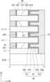
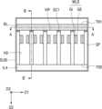
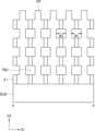
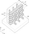
도 3은 본 개시의 일 실시예에 따른 반도체 메모리 소자를 나타내는 사시도이다. 도 4a 내지 도 4c는 각각 도 3의 A-A' 선, B-B' 선, 및 C-C' 선에 따른 단면도들이다. 이하에서는 도 2 에 도시된 반도체 메모리 소자와 도 3 및 도 4a 내지 도 4c에 도시된 반도체 메모리 소자 사이의 차이점이 설명된다.FIG. 3 is a perspective view showing a semiconductor memory device according to one embodiment of the present disclosure. FIGS. 4A to 4C are cross-sectional views taken along lines A-A', B-B', and C-C' of FIG. 3, respectively. Hereinafter, differences between the semiconductor memory device illustrated in FIG. 2 and the semiconductor memory devices illustrated in FIG. 3 and FIGS. 4A to 4C will be described.
도 3 및 도 4a 내지 도 4c를 참조하면, 복수의 제1 절연 층(IL1)은 복수의 반도체 패턴(SP)을 수직 방향(D3)으로 이격시킬 수 있다. 즉, 복수의 제1 절연 층(IL1)은 복수의 반도체 패턴(SP)과 교대할 수 있다. 복수의 비트 라인(BL)은 복수의 제1 절연 층(IL1) 사이에 위치할 수 있다. 즉, 복수의 제1 절연 층(IL1)은 복수의 비트 라인(BL)과 교대할 수 있다. 제1 절연 층(IL1)은 실리콘 산화물(SiO2), 실리콘 질화물(SiN), 실리콘 산질화물(SiON), 또는 이들의 조합을 포함할 수 있다.Referring to FIGS. 3 and 4A to 4C, a plurality of first insulating layers (IL1) can space a plurality of semiconductor patterns (SP) apart in a vertical direction (D3). That is, a plurality of first insulating layers (IL1) can alternate with a plurality of semiconductor patterns (SP). A plurality of bit lines (BL) can be positioned between a plurality of first insulating layers (IL1). That is, a plurality of first insulating layers (IL1) can alternate with a plurality of bit lines (BL). The first insulating layers (IL1) can include silicon oxide (SiO2 ), silicon nitride (SiN), silicon oxynitride (SiON), or a combination thereof.
수직 절연 층(VIP)은 제1 수평 방향(D1)으로 이웃한 한 쌍의 반도체 패턴(SP) 사이에 위치할 수 있다. 수직 절연 층(VIP)은 수직 방향(D3)으로 연장될 수 있다. 수직 절연 층(VIP)은 제1 수평 방향(D1)으로 이웃한 한 쌍의 워드 라인 구조체(WLS) 사이에 위치할 수 있다. 수직 절연 층(VIP)은 실리콘 산화물(SiO2), 실리콘 질화물(SiN), 실리콘 산질화물(SiON), 또는 이들의 조합을 포함할 수 있다.A vertical insulating layer (VIP) can be positioned between a pair of adjacent semiconductor patterns (SPs) in a first horizontal direction (D1). The vertical insulating layer (VIP) can extend in the vertical direction (D3). The vertical insulating layer (VIP) can be positioned between a pair of adjacent word line structures (WLSs) in the first horizontal direction (D1). The vertical insulating layer (VIP) can include silicon oxide (SiO2 ), silicon nitride (SiN), silicon oxynitride (SiON), or a combination thereof.
일부 실시에에서, 비트 라인(BL)과 반도체 패턴(SP) 사이에 제1 실리사이드 패턴(SC1)이 위치할 수 있다. 비트 라인(BL)은 제1 실리사이드 패턴(SC1)을 통해 제1 소스/드레인 영역(SD1)에 전기적으로 연결될 수 있다. 제1 실리사이드 패턴(SC1)은 금속 실리사이드를 포함할 수 있다.In some embodiments, a first silicide pattern (SC1) may be positioned between a bit line (BL) and a semiconductor pattern (SP). The bit line (BL) may be electrically connected to a first source/drain region (SD1) through the first silicide pattern (SC1). The first silicide pattern (SC1) may include a metal silicide.
각각의 정보 저장 요소(DS)는 제2 소스/드레인 영역(SD2)에 연결되는 제1 전극(EL1), 제1 전극(EL1) 상의 제2 전극(EL2), 및 제1 전극(EL1)과 제2 전극(EL2) 사이의 유전 층(DL)을 포함할 수 있다. 복수의 정보 저장 요소(DS)는 하나의 유전 층(DL) 및 하나의 제2 전극(EL2)을 공유할 수 있다. 다시 말해, 복수의 제1 전극(EL1), 하나의 유전 층(DL), 및 하나의 제2 전극(EL2)이 복수의 정보 저장 요소(DS)를 형성할 수 있다. 제1 전극(EL1)은 복수의 제1 절연 층(IL1) 사이에 위치할 수 있다.Each information storage element (DS) can include a first electrode (EL1) connected to a second source/drain region (SD2), a second electrode (EL2) on the first electrode (EL1), and a dielectric layer (DL) between the first electrode (EL1) and the second electrode (EL2). A plurality of information storage elements (DS) can share one dielectric layer (DL) and one second electrode (EL2). In other words, a plurality of first electrodes (EL1), one dielectric layer (DL), and one second electrode (EL2) can form a plurality of information storage elements (DS). The first electrode (EL1) can be located between a plurality of first insulating layers (IL1).
제1 전극(EL1)은 제2 소스/드레인 영역(SD2)에 전기적으로 연결되는 제1 베이스부(PB1), 및 제1 베이스부(PB1)로부터 제2 수평 방향(D2)으로 돌출되는 제1 돌출부(PP1)를 포함할 수 있다. 제1 베이스부(PB1) 및 제1 돌출부(PP1)는 내부 공간을 정의할 수 있다. 제2 전극(EL2)은 제2 베이스부(PB2) 및 제2 베이스부(PB2)로부터 제2 수평 방향(D2)에 반대인 방향으로 돌출된 복수의 제2 돌출부(PP2)를 포함할 수 있다. 각각의 제2 돌출부(PP2)는 제1 베이스부(PB1) 및 제1 돌출부(PP1)에 의해 정의되는 상기 공간 내에 위치할 수 있다.The first electrode (EL1) may include a first base portion (PB1) electrically connected to the second source/drain region (SD2), and a first protrusion portion (PP1) protruding from the first base portion (PB1) in a second horizontal direction (D2). The first base portion (PB1) and the first protrusion portion (PP1) may define an internal space. The second electrode (EL2) may include a second base portion (PB2) and a plurality of second protrusion portions (PP2) protruding from the second base portion (PB2) in a direction opposite to the second horizontal direction (D2). Each of the second protrusion portions (PP2) may be positioned within the space defined by the first base portion (PB1) and the first protrusion portion (PP1).
제1 전극(EL1) 및 제2 전극(EL2) 각각은 금속 물질, 예를 들어 티타늄(Ti), 탄탈륨(Ta), 텅스텐(W), 구리(Cu), 알루미늄(Al), 티타늄 질화물(TiN), 탄탈륨 질화물(TaN), 도핑된 실리콘(doped Si), 도핑된 게르마늄(doped Ge), 또는 이들의 조합을 포함할 수 있다. 유전 층(DL)은 고유전 물질, 예를 들어 하프늄 산화물(HfO2), 하프늄 실리콘 산화물(HfSiO2), 란탄 산화물(LaO), 지르코늄산화물(ZrO2), 지르코늄 실리콘 산화물(ZrSiO2), 탄탈륨 산화물(Ta2O5), 티타늄 산화물(TiO2), 바륨 스트론튬 티타늄 산화물(BaSrTiO3), 바륨 티타늄 산화물(BaTiO3), 스트론튬 티타늄 산화물(SrTiO3), 리튬 산화물(Li2O), 알루미늄 산화물(Al2O-3), 납 스칸듐 탄탈륨 산화물(PbScTaO), 납 아연 니오브산염(PbZnNbO3), 또는 이들의 조합을 포함할 수 있다.Each of the first electrode (EL1) and the second electrode (EL2) may include a metal material, such as titanium (Ti), tantalum (Ta), tungsten (W), copper (Cu), aluminum (Al), titanium nitride (TiN), tantalum nitride (TaN), doped silicon (doped Si), doped germanium (doped Ge), or a combination thereof. The dielectric layer (DL) may include a high-k material, such as hafnium oxide (HfO2 ), hafnium silicon oxide (HfSiO2 ), lanthanum oxide (LaO), zirconium oxide (ZrO2 ), zirconium silicon oxide (ZrSiO2 ), tantalum oxide (Ta2 O5 ), titanium oxide (TiO2 ), barium strontium titanium oxide (BaSrTiO3 ), barium titanium oxide (BaTiO3 ), strontium titanium oxide (SrTiO3 ), lithium oxide (Li2 O), aluminum oxide (Al2 O-3 ), lead scandium tantalum oxide (PbScTaO), lead zinc niobate (PbZnNbO3 ), or combinations thereof.
반도체 패턴(SP)과 제1 전극(EL1) 사이에 제2 실리사이드 패턴(SC2)이 위치할 수 있다. 제1 전극(EL1)은 제2 실리사이드 패턴(SC2)을 통해 제2 소스/드레인 영역(SD2)에 전기적으로 연결될 수 있다. 제2 실리사이드 패턴(SC2)은 금속 실리사이드를 포함할 수 있다.A second silicide pattern (SC2) may be positioned between the semiconductor pattern (SP) and the first electrode (EL1). The first electrode (EL1) may be electrically connected to the second source/drain region (SD2) through the second silicide pattern (SC2). The second silicide pattern (SC2) may include a metal silicide.
복수의 반도체 패턴(SP)은 단결정일 수 있다. 복수의 반도체 패턴(SP) 중 적어도 하나의 결정 방향은 복수의 반도체 패턴(SP) 중 다른 하나의 결정 방향과 상이할 수 있다. 도 4c를 참조하면, 복수의 반도체 패턴(SP) 중 적어도 하나는 그 반도체 패턴(SP)의 하면 또는 상면에 대하여 비스듬하게 연장되는 격자 결함(LD)을 가질 수 있다. 예를 들어, 복수의 반도체 패턴(SP)은 수직 방향(D3)으로 서로 이격되는 제1 반도체 패턴(SP1) 및 제2 반도체 패턴(SP2)을 포함할 수 있으며, 제1 반도체 패턴(SP1) 및 제2 반도체 패턴(SP2) 중 적어도 하나는 격자 결함(LD)을 포함할 수 있다. 제1 수평 방향(D1)에 수직한 반도체 메모리 소자의 절단면 상에서, 격자 결함(LD)은 직선으로 나타날 수 있다. 격자 결함(LD)과 반도체 패턴(SP)의 상면 또는 하면 사이의 각도(θ)는 약 50도 내지 약 60도일 수 있다. 예를 들어, 상기 각도(θ)는 약 54.7도일 수 있다.The plurality of semiconductor patterns (SP) may be single crystals. The crystal direction of at least one of the plurality of semiconductor patterns (SP) may be different from the crystal direction of another one of the plurality of semiconductor patterns (SP). Referring to FIG. 4C, at least one of the plurality of semiconductor patterns (SP) may have a lattice defect (LD) extending obliquely with respect to a lower surface or an upper surface of the semiconductor pattern (SP). For example, the plurality of semiconductor patterns (SP) may include a first semiconductor pattern (SP1) and a second semiconductor pattern (SP2) spaced apart from each other in a vertical direction (D3), and at least one of the first semiconductor pattern (SP1) and the second semiconductor pattern (SP2) may include a lattice defect (LD). On a cross-section of the semiconductor memory device perpendicular to the first horizontal direction (D1), the lattice defect (LD) may appear as a straight line. The angle (θ) between the lattice defect (LD) and the upper surface or the lower surface of the semiconductor pattern (SP) may be about 50 degrees to about 60 degrees. For example, the angle (θ) may be about 54.7 degrees.
예를 들어, 복수의 반도체 패턴(SP)은 제2 반도체 패턴(SP2)을 포함하고, 복수의 제1 절연 층(IL1)은 제2 반도체 패턴(SP2)의 상면 상의 상부 절연 층(IL1-2) 및 제2 반도체 패턴(SP2)의 하면 상의 하부 절연 층(IL1-1)을 포함할 수 있다. 반도체 패턴(SP)은 상부 절연 층(IL1-2)의 하면 및 하부 절연 층(IL1-1)의 상면 중 적어도 하나에 대하여 비스듬하게 연장되는 격자 결함(LD)을 가질 수 있다. 격자 결함(LD)은 상부 절연 층(IL1-2)의 하면 및 하부 절연 층(IL1-1)의 상면 중 적어도 하나와 접촉할 수 있다. 격자 결함(LD)과 상부 절연 층(IL1-2)의 하면 및 하부 절연 층(IL1-1)의 상면 중 적어도 하나 사이의 각도는 50도 내지 60도일 수 있다.For example, the plurality of semiconductor patterns (SP) may include second semiconductor patterns (SP2), and the plurality of first insulating layers (IL1) may include an upper insulating layer (IL1-2) on an upper surface of the second semiconductor pattern (SP2) and a lower insulating layer (IL1-1) on a lower surface of the second semiconductor pattern (SP2). The semiconductor pattern (SP) may have a lattice defect (LD) extending obliquely with respect to at least one of the lower surface of the upper insulating layer (IL1-2) and the upper surface of the lower insulating layer (IL1-1). The lattice defect (LD) may contact at least one of the lower surface of the upper insulating layer (IL1-2) and the upper surface of the lower insulating layer (IL1-1). An angle between the lattice defect (LD) and at least one of the lower surface of the upper insulating layer (IL1-2) and the upper surface of the lower insulating layer (IL1-1) may be 50 to 60 degrees.
도 5a 내지 도 5f는 본 개시의 일 실시예에 따른 반도체 메모리 소자를 제조하기 위한 적층 구조체를 제조하는 방법들을 설명하기 위한 단면도들이다.FIGS. 5A to 5F are cross-sectional views illustrating methods for manufacturing a laminated structure for manufacturing a semiconductor memory device according to one embodiment of the present disclosure.
도 5a를 참조하면, 기판(SUB) 상에 제1 몰드 구조체(MS)가 형성될 수 있다. 제1 몰드 구조체(MS)는 복수의 제1 절연 층(IL1) 및 복수의 제2 절연 층(IL2)을 기판(SUB) 상에 교대로 적층시킴으로써 형성될 수 있다. 제1 절연 층(IL1) 및 제2 절연 층(IL2)은 실리콘 산화물(SiO2), 실리콘 질화물(SiN), 실리콘 산질화물(SiON), 또는 이들의 조합을 포함할 수 있다. 제1 절연 층(IL2)과 제2 절연 층(IL2)은 서로에 대하여 식각 선택비를 가질 수 있다. 예를 들어, 제1 절연 층(IL1)은 실리콘 산화물(SiO2)을 포함할 수 있고, 제2 절연 층(IL2)은 실리콘 질화물(SiN)을 포함할 수 있다.Referring to FIG. 5a, a first mold structure (MS) may be formed on a substrate (SUB). The first mold structure (MS) may be formed by alternately stacking a plurality of first insulating layers (IL1) and a plurality of second insulating layers (IL2) on the substrate (SUB). The first insulating layer (IL1) and the second insulating layer (IL2) may include silicon oxide (SiO2 ), silicon nitride (SiN), silicon oxynitride (SiON), or a combination thereof. The first insulating layer (IL2) and the second insulating layer (IL2) may have etching selectivities with respect to each other. For example, the first insulating layer (IL1) may include silicon oxide (SiO2 ), and the second insulating layer (IL2) may include silicon nitride (SiN).
제1 몰드 구조체(MS) 내에 복수의 제1 트렌치(TR1)가 형성될 수 있다. 각각의 제1 트렌치(TR1)는 수직 방향(D3)으로 연장될 수 있으며, 복수의 제1 트렌치(TR1)는 제2 수평 방향(D2)으로 이격될 수 있다. 제1 트렌치(TR1)는 기판(SUB)을 노출시키는 것으로 도 5a에 도시되었으나, 일부 실시예에서, 제1 트렌치(TR1)는 기판(SUB)을 노출시키지 않을 수 있다.A plurality of first trenches (TR1) may be formed within the first mold structure (MS). Each of the first trenches (TR1) may extend in a vertical direction (D3), and the plurality of first trenches (TR1) may be spaced apart from each other in a second horizontal direction (D2). The first trench (TR1) is illustrated in FIG. 5A as exposing the substrate (SUB), but in some embodiments, the first trench (TR1) may not expose the substrate (SUB).
도 5b를 참조하면, 제2 절연 층(IL2)을 측방향으로 식각함으로써 복수의 제1 리세스(RS1)가 형성될 수 있다. 예를 들어, 제2 절연 층(IL2)을 선택적으로 습식 식각함으로써 복수의 제1 리세스(RS1)가 형성될 수 있다. 각각의 제1 리세스(RS1)는 이웃한 두 제1 절연 층(IL1), 및 이웃한 두 제1 절연 층(IL1) 사이의 제2 절연 층(IL2)에 의해 정의될 수 있다.Referring to FIG. 5b, a plurality of first recesses (RS1) can be formed by etching the second insulating layer (IL2) laterally. For example, a plurality of first recesses (RS1) can be formed by selectively wet etching the second insulating layer (IL2). Each first recess (RS1) can be defined by two adjacent first insulating layers (IL1) and a second insulating layer (IL2) between two adjacent first insulating layers (IL1).
도 5c를 참조하면, 다결정 반도체 층(PS)이 복수의 제1 리세스(RS1) 내에 형성될 수 있다. 예를 들어, 제1 리세스(RS1)를 채우도록 다결정 반도체 층(PS)이 증착되고, 다결정 반도체 층(PS)이 측방향으로 식각될 수 있다. 다결정 반도체 층(PS)은 에피택시얼 공정이 아닌 화학 기상 증착(chemical vapor deposition, CVD) 공정에 의해 형성될 수 있다. 따라서 다결정 반도체 층(PS)을 형성하는 것은 에피택시얼 공정에 의해 단결정 반도체 시드를 형성하는 것보다 용이할 수 있다. 다결정 반도체 층(PS)은 반도체 물질, 예를 들어, 실리콘(Si), 게르마늄(Ge), 또는 실리콘-게르마늄(SiGe)을 포함할 수 있다.Referring to FIG. 5c, a polycrystalline semiconductor layer (PS) may be formed within a plurality of first recesses (RS1). For example, a polycrystalline semiconductor layer (PS) may be deposited to fill the first recesses (RS1), and the polycrystalline semiconductor layer (PS) may be etched laterally. The polycrystalline semiconductor layer (PS) may be formed by a chemical vapor deposition (CVD) process rather than an epitaxial process. Therefore, forming the polycrystalline semiconductor layer (PS) may be easier than forming a single-crystal semiconductor seed by an epitaxial process. The polycrystalline semiconductor layer (PS) may include a semiconductor material, for example, silicon (Si), germanium (Ge), or silicon-germanium (SiGe).
도 5d를 참조하면, 제1 리세스(RS1)를 채우도록 수평 반도체 패턴(HSL)이 형성될 수 있다. 수평 반도체 패턴(HSL)은 다결정 반도체 층(PS)을 시드로 사용하여 에피??시얼 성장에 의해 형성될 수 있다. 비록 시드는 다결정 이지만, 좁은 제1 리세스(RS1) 내의 공간에서 수평 반도체 패턴(HSL)이 형성되므로 수평 반도체 패턴(HSL)은 단결정으로 성장할 수 있다. 다만, 다결정 반도체 층(PS)을 시드로 사용하므로 결정 방향이 상이한 부분들로부터 성장된 수평 반도체 패턴(HSL)들은 상이한 결정 방향을 가질 수 있다. 또한, 수평 반도체 패턴(HSL)은 격자 결함(LD)을 포함할 수 있다. 다결정 반도체 층(PS)으로부터 성장하던 수평 반도체 패턴(HSL)이 제1 절연 층(IL1)을 만나면 격자 결함(LD)이 형성될 수 있다. 격자 결함(LD)은 제2 수평 방향(D2)에 대하여 약 50 도 내지 약 60도의 각도(θ)를 가질 수 있다.Referring to FIG. 5d, a horizontal semiconductor pattern (HSL) can be formed to fill the first recess (RS1). The horizontal semiconductor pattern (HSL) can be formed by epitaxial growth using a polycrystalline semiconductor layer (PS) as a seed. Although the seed is polycrystalline, since the horizontal semiconductor pattern (HSL) is formed in a space within the narrow first recess (RS1), the horizontal semiconductor pattern (HSL) can grow as a single crystal. However, since the polycrystalline semiconductor layer (PS) is used as a seed, horizontal semiconductor patterns (HSL) grown from portions having different crystal directions may have different crystal directions. In addition, the horizontal semiconductor pattern (HSL) may include a lattice defect (LD). When the horizontal semiconductor pattern (HSL) grown from the polycrystalline semiconductor layer (PS) meets the first insulating layer (IL1), a lattice defect (LD) may be formed. The lattice defect (LD) can have an angle (θ) of about 50 degrees to about 60 degrees with respect to the second horizontal direction (D2).
도 5e를 참조하면, 제1 트렌치(TR1) 내를 채우는 제3 절연 층(IL3)이 형성될 수 있다. 제3 절연 층(IL3)은 실리콘 산화물(SiO2), 실리콘 질화물(SiN), 또는 실리콘 산질화물(SiON)을 포함할 수 있다.Referring to FIG. 5e, a third insulating layer (IL3) may be formed to fill the first trench (TR1). The third insulating layer (IL3) may include silicon oxide (SiO2 ), silicon nitride (SiN), or silicon oxynitride (SiON).
도 5e 및 도 5f를 참조하면, 다결정 반도체 층(PS) 및 제2 절연 층(IL2)이 제거되도록 제2 트렌치(TR2)가 형성될 수 있다. 제2 트렌치(TR2)에 제4 절연 층(IL4)이 채워질 수 있다. 제4 절연 층(IL4)은 실리콘 산화물(SiO2), 실리콘 질화물(SiN), 또는 실리콘 산질화물(SiON)을 포함할 수 있다.Referring to FIGS. 5e and 5f, a second trench (TR2) can be formed so that the polycrystalline semiconductor layer (PS) and the second insulating layer (IL2) are removed. A fourth insulating layer (IL4) can be filled in the second trench (TR2). The fourth insulating layer (IL4) can include silicon oxide (SiO2 ), silicon nitride (SiN), or silicon oxynitride (SiON).
도 5a 내지 도 5f를 참조하여 설명한 바에 따라 본 개시의 일 실시예에 따른 반도체 메모리 소자를 제조하는데 사용되는 적층 구조체(100)가 제조될 수 있다. 적층 구조체(100)는 기판(SUB) 상에 수직 방향(D3)으로 교대로 적층된 복수의 제1 절연 층(IL1) 및 복수의 수평 반도체 층(HSL)을 포함할 수 있다. 또한, 적층 구조체(100)는 각각이 적층 구조체(100)를 관통하며 제2 수평 방향(D2)으로 서로 이격된 복수의 제3 절연 층(IL3)을 더 포함할 수 있다. 적층 구조체(100)는 이웃한 두 제3 절연 층(IL3) 사이의 제4 절연 층(IL4)을 더 포함할 수 있다. 제4 절연 층(IL4)은 제3 절연 층(IL3)으로부터 제2 수평 방향(D2)으로 떨어질 수 있다. 제1 절연 층(IL1) 및 수평 반도체 층(HSL)은 제3 절연 층(IL3)과 제4 절연 층(IL4) 사이에 연장될 수 있다.According to the description with reference to FIGS. 5A to 5F, a laminated structure (100) used for manufacturing a semiconductor memory device according to an embodiment of the present disclosure can be manufactured. The laminated structure (100) can include a plurality of first insulating layers (IL1) and a plurality of horizontal semiconductor layers (HSL) alternately laminated in a vertical direction (D3) on a substrate (SUB). In addition, the laminated structure (100) can further include a plurality of third insulating layers (IL3) each penetrating the laminated structure (100) and spaced apart from each other in a second horizontal direction (D2). The laminated structure (100) can further include a fourth insulating layer (IL4) between two adjacent third insulating layers (IL3). The fourth insulating layer (IL4) can be spaced apart from the third insulating layer (IL3) in the second horizontal direction (D2). The first insulating layer (IL1) and the horizontal semiconductor layer (HSL) can extend between the third insulating layer (IL3) and the fourth insulating layer (IL4).
도 6a 내지 도 6e는 본 개시의 일 실시예에 따른 반도체 메모리 소자를 제조하기 위한 적층 구조체를 제조하는 방법들을 설명하기 위한 단면도들이다.FIGS. 6A to 6E are cross-sectional views illustrating methods for manufacturing a laminated structure for manufacturing a semiconductor memory device according to one embodiment of the present disclosure.
도 6a를 참조하면, 기판(SUB) 상에 제2 몰드 구조체(MS2)가 형성될 수 있다. 제2 몰드 구조체(MS2)는 복수의 제1 절연 층(IL1) 및 복수의 다결정 반도체 층(PS)을 기판(SUB) 상에 교대로 적층시킴으로써 형성될 수 있다. 다결정 반도체 층(PS)은 반도체 물질, 예를 들어 실리콘(Si), 게르마늄(Ge), 또는 실리콘-게르마늄(SiGe)을 포함할 수 있다. 제1 절연 층(IL1)은 실리콘 산화물(SiO2), 실리콘 질화물(SiN), 실리콘 산질화물(SiON), 또는 이들의 조합을 포함할 수 있다. 다결정 반도체 층(PS)은 CVD 공정에 의해 형성될 수 있으므로 공정 비용 및 난이도가 감소될 수 있다.Referring to FIG. 6a, a second mold structure (MS2) can be formed on a substrate (SUB). The second mold structure (MS2) can be formed by alternately stacking a plurality of first insulating layers (IL1) and a plurality of polycrystalline semiconductor layers (PS) on the substrate (SUB). The polycrystalline semiconductor layers (PS) can include a semiconductor material, such as silicon (Si), germanium (Ge), or silicon-germanium (SiGe). The first insulating layer (IL1) can include silicon oxide (SiO2 ), silicon nitride (SiN), silicon oxynitride (SiON), or a combination thereof. Since the polycrystalline semiconductor layers (PS) can be formed by a CVD process, process cost and difficulty can be reduced.
제2 몰드 구조체(MS2) 내에 복수의 제1 트렌치(TR1)가 형성될 수 있다. 각각의 제1 트렌치(TR1)는 수직 방향(D3)으로 연장될 수 있으며, 복수의 제1 트렌치(TR1)는 제2 수평 방향(D2)으로 이격될 수 있다. 제1 트렌치(TR1)는 기판(SUB)을 노출시키는 것으로 도 6a에 도시되었으나, 일부 실시예에서, 제1 트렌치(TR1)는 기판(SUB)을 노출시키지 않을 수 있다.A plurality of first trenches (TR1) may be formed within the second mold structure (MS2). Each of the first trenches (TR1) may extend in the vertical direction (D3), and the plurality of first trenches (TR1) may be spaced apart from each other in the second horizontal direction (D2). The first trench (TR1) is illustrated in FIG. 6A as exposing the substrate (SUB), but in some embodiments, the first trench (TR1) may not expose the substrate (SUB).
도 6b를 참조하면, 다결정 반도체 층(PS)을 선택적으로 측방향으로 식각함으로써 제1 리세스(RS1)가 형성될 수 있다. 각각의 제1 리세스(RS1)는 이웃한 두 제1 절연 층(IL1), 및 이웃한 두 제1 절연 층(IL1) 사이의 다결정 반도체 층(PS)에 의해 정의될 수 있다.Referring to FIG. 6b, a first recess (RS1) can be formed by selectively etching the polycrystalline semiconductor layer (PS) laterally. Each first recess (RS1) can be defined by two adjacent first insulating layers (IL1) and the polycrystalline semiconductor layer (PS) between the two adjacent first insulating layers (IL1).
도 6c를 참조하면, 제1 리세스(RS1)를 채우도록 수평 반도체 패턴(HSL)이 형성될 수 있다. 수평 반도체 패턴(HSL)은 다결정 반도체 층(PS)을 시드로 사용하여 에피택시얼 성장에 의해 형성될 수 있다. 비록 시드는 다결정 이지만, 좁은 제1 리세스(RS1) 내의 공간에서 수평 반도체 패턴(HSL)이 형성되므로 수평 반도체 패턴(HSL)은 단결정으로 성장할 수 있다. 다만, 다결정 반도체 층(PS)을 시드로 사용하므로 결정 방향이 상이한 부분들로부터 성장된 수평 반도체 패턴(HSL)들은 상이한 결정 방향을 가질 수 있다. 또한, 수평 반도체 패턴(HSL)은 격자 결함(LD)을 포함할 수 있다. 다결정 반도체 층(PS)으로부터 성장하던 수평 반도체 패턴(HSL)이 제1 절연 층(IL1)을 만나면 격자 결함(LD)이 형성될 수 있다. 격자 결함(LD)은 제2 수평 방향(D2)에 대하여 약 50 도 내지 약 60도의 각도(θ)를 가질 수 있다.Referring to FIG. 6c, a horizontal semiconductor pattern (HSL) can be formed to fill the first recess (RS1). The horizontal semiconductor pattern (HSL) can be formed by epitaxial growth using a polycrystalline semiconductor layer (PS) as a seed. Although the seed is polycrystalline, since the horizontal semiconductor pattern (HSL) is formed in the space within the narrow first recess (RS1), the horizontal semiconductor pattern (HSL) can grow as a single crystal. However, since the polycrystalline semiconductor layer (PS) is used as a seed, horizontal semiconductor patterns (HSL) grown from portions having different crystal directions may have different crystal directions. In addition, the horizontal semiconductor pattern (HSL) may include a lattice defect (LD). When the horizontal semiconductor pattern (HSL) grown from the polycrystalline semiconductor layer (PS) meets the first insulating layer (IL1), a lattice defect (LD) may be formed. The lattice defect (LD) can have an angle (θ) of about 50 degrees to about 60 degrees with respect to the second horizontal direction (D2).
도 6d를 참조하면, 제1 트렌치(TR1)를 채우는 제3 절연 층(IL3)이 형성될 수 있다. 제3 절연 층(IL3)은 실리콘 산화물(SiO2), 실리콘 질화물(SiN), 또는 실리콘 산질화물(SiON)을 포함할 수 있다.Referring to FIG. 6d, a third insulating layer (IL3) filling the first trench (TR1) may be formed. The third insulating layer (IL3) may include silicon oxide (SiO2 ), silicon nitride (SiN), or silicon oxynitride (SiON).
도 6d 및 도 6e를 참조하면, 다결정 반도체 층(PS)이 제거되도록 제2 트렌치(TR2)가 형성될 수 있다. 제2 트렌치(TR2) 내에 제4 절연 층(IL4)이 채워질 수 있다. 도 6a 내지 도 6e를 참조하여 설명한 바에 따라 본 개시의 일 실시예에 따른 반도체 메모리 소자를 제조하는데 사용되는 적층 구조체(100)가 제조될 수 있다.Referring to FIGS. 6d and 6e, a second trench (TR2) may be formed so that the polycrystalline semiconductor layer (PS) is removed. A fourth insulating layer (IL4) may be filled within the second trench (TR2). As described with reference to FIGS. 6a to 6e, a laminated structure (100) used for manufacturing a semiconductor memory device according to an embodiment of the present disclosure may be manufactured.
도 7a 내지 도 7g는 본 개시의 일 실시예에 따른 반도체 메모리 소자를 제조하기 위한 적층 구조체를 제조하는 방법들을 설명하기 위한 단면도들이다.FIGS. 7A to 7G are cross-sectional views illustrating methods for manufacturing a laminated structure for manufacturing a semiconductor memory device according to one embodiment of the present disclosure.
도 7a를 참조하면, 기판(SUB) 상에 제1 몰드 구조체(MS)가 형성될 수 있다. 제1 몰드 구조체(MS)는 복수의 제1 절연 층(IL1) 및 복수의 제2 절연 층(IL2)을 기판(SUB) 상에 교대로 적층시킴으로써 형성될 수 있다. 제1 절연 층(IL1) 및 제2 절연 층(IL2)은 실리콘 산화물(SiO2), 실리콘 질화물(SiN), 실리콘 산질화물(SiON), 또는 이들의 조합을 포함할 수 있다. 제1 절연 층(IL2)과 제2 절연 층(IL2)은 서로에 대하여 식각 선택비를 가질 수 있다. 예를 들어, 제1 절연 층(IL1)은 실리콘 산화물(SiO2)을 포함할 수 있고, 제2 절연 층(IL2)은 실리콘 질화물(SiN)을 포함할 수 있다.Referring to FIG. 7a, a first mold structure (MS) may be formed on a substrate (SUB). The first mold structure (MS) may be formed by alternately stacking a plurality of first insulating layers (IL1) and a plurality of second insulating layers (IL2) on the substrate (SUB). The first insulating layer (IL1) and the second insulating layer (IL2) may include silicon oxide (SiO2 ), silicon nitride (SiN), silicon oxynitride (SiON), or a combination thereof. The first insulating layer (IL2) and the second insulating layer (IL2) may have an etching selectivity with respect to each other. For example, the first insulating layer (IL1) may include silicon oxide (SiO2 ), and the second insulating layer (IL2) may include silicon nitride (SiN).
몰드 구조체(MS) 내에 복수의 제1 트렌치(TR1)가 형성될 수 있다. 각각의 제1 트렌치(TR1)는 수직 방향(D3)으로 연장될 수 있으며, 복수의 제1 트렌치(TR1)는 제2 수평 방향(D2)으로 이격될 수 있다. 제1 트렌치(TR1)는 기판(SUB)을 노출시키는 것으로 도 7a에 도시되었으나, 일부 실시예에서, 제1 트렌치(TR1)는 기판(SUB)을 노출시키지 않을 수 있다.A plurality of first trenches (TR1) may be formed within the mold structure (MS). Each of the first trenches (TR1) may extend in a vertical direction (D3), and the plurality of first trenches (TR1) may be spaced apart from each other in a second horizontal direction (D2). The first trench (TR1) is illustrated in FIG. 7A as exposing the substrate (SUB), but in some embodiments, the first trench (TR1) may not expose the substrate (SUB).
도 7b를 참조하면, 제1 트렌치(TR1)의 표면 상에 다결정 반도체 층(PS)이 형성될 수 있다. 다음으로, 제1 트렌치(TR1)를 채우도록 다결정 반도체 층(PS) 상에 제5 층간 절연 층(IL5)이 형성될 수 있다. 제5 층간 절연 층(IL5)은 실리콘 산화물(SiO2), 실리콘 질화물(SiN), 실리콘 산질화물(SiON), 또는 이들의 조합을 포함할 수 있다. 다른 실시예에서, 제1 트렌치(TR1)가 다결정 반도체 층(PS)에 의해서만 채워질 수 있다. 다결정 반도체 층(PS)은 CVD 공정에 의해 형성될 수 있으므로 공정 비용 및 난이도가 감소될 수 있다.Referring to FIG. 7b, a polycrystalline semiconductor layer (PS) may be formed on a surface of the first trench (TR1). Next, a fifth interlayer insulating layer (IL5) may be formed on the polycrystalline semiconductor layer (PS) to fill the first trench (TR1). The fifth interlayer insulating layer (IL5) may include silicon oxide (SiO2 ), silicon nitride (SiN), silicon oxynitride (SiON), or a combination thereof. In another embodiment, the first trench (TR1) may be filled only by the polycrystalline semiconductor layer (PS). Since the polycrystalline semiconductor layer (PS) may be formed by a CVD process, process cost and difficulty may be reduced.
도 7c를 참조하면, 복수의 제1 트렌치(TR1) 사이에 몰드 구조체(MS)를 수직 방향(D3)으로 관통하는 제2 트렌치(TR2)가 형성될 수 있다. 도 7c에는 제2 트렌치(TR2)가 기판(SUB)을 노출시키는 것으로 도시되었으나, 일부 실시예에서, 제2 트렌치(TR2)는 기판(SUB)을 노출시키지 않을 수 있다.Referring to FIG. 7c, a second trench (TR2) may be formed between a plurality of first trenches (TR1) to penetrate the mold structure (MS) in the vertical direction (D3). Although FIG. 7c illustrates that the second trench (TR2) exposes the substrate (SUB), in some embodiments, the second trench (TR2) may not expose the substrate (SUB).
도 7c 및 도 7d를 참조하면, 제2 절연 층(IL2)을 제거함으로써 복수의 제1 리세스(RS1)를 형성할 수 있다. 복수의 제1 리세스(RS1)는 다결정 반도체 층(PS)을 노출시킬 수 있다. 각각의 제1 리세스(RS1)는 이웃한 두 제1 절연 층(IL1) 및 다결정 반도체 층(PS)에 의해 정의될 수 있다.Referring to FIGS. 7c and 7d, a plurality of first recesses (RS1) can be formed by removing the second insulating layer (IL2). The plurality of first recesses (RS1) can expose the polycrystalline semiconductor layer (PS). Each first recess (RS1) can be defined by two adjacent first insulating layers (IL1) and the polycrystalline semiconductor layer (PS).
도 7e를 참조하면, 제1 리세스(RS1)를 채우도록 수평 반도체 패턴(HSL)이 형성될 수 있다. 수평 반도체 패턴(HSL)은 다결정 반도체 층(PS)을 시드로 사용하여 에피택시얼 성장에 의해 형성될 수 있다. 비록 시드는 다결정 이지만, 좁은 제1 리세스(RS1) 내의 공간에서 수평 반도체 패턴(HSL)이 형성되므로 수평 반도체 패턴(HSL)은 단결정으로 성장할 수 있다. 다만, 다결정 반도체 층(PS)을 시드로 사용하므로 결정 방향이 상이한 부분들로부터 성장된 수평 반도체 패턴(HSL)들은 상이한 결정 방향을 가질 수 있다. 또한, 수평 반도체 패턴(HSL)은 격자 결함(LD)을 포함할 수 있다. 다결정 반도체 층(PS)으로부터 성장하던 수평 반도체 패턴(HSL)이 제1 절연 층(IL1)을 만나면 격자 결함(LD)이 형성될 수 있다. 격자 결함(LD)은 제2 수평 방향(D2)에 대하여 약 50 도 내지 약 60도의 각도(θ)를 가질 수 있다.Referring to FIG. 7e, a horizontal semiconductor pattern (HSL) can be formed to fill the first recess (RS1). The horizontal semiconductor pattern (HSL) can be formed by epitaxial growth using a polycrystalline semiconductor layer (PS) as a seed. Although the seed is polycrystalline, since the horizontal semiconductor pattern (HSL) is formed in the space within the narrow first recess (RS1), the horizontal semiconductor pattern (HSL) can grow as a single crystal. However, since the polycrystalline semiconductor layer (PS) is used as a seed, horizontal semiconductor patterns (HSL) grown from portions having different crystal directions may have different crystal directions. In addition, the horizontal semiconductor pattern (HSL) may include a lattice defect (LD). When the horizontal semiconductor pattern (HSL) grown from the polycrystalline semiconductor layer (PS) meets the first insulating layer (IL1), a lattice defect (LD) may be formed. The lattice defect (LD) can have an angle (θ) of about 50 degrees to about 60 degrees with respect to the second horizontal direction (D2).
도 7f를 참조하면, 제2 트렌치(TR2) 내에 제4 절연 층(IL4)이 형성될 수 있다.Referring to FIG. 7f, a fourth insulating layer (IL4) can be formed within the second trench (TR2).
도 7f 및 도 7g를 참조하면, 제1 트렌치(TR1) 내의 다결정 반도체 층(PS) 및 제5 절연 층(IL5)이 제거될 수 있다. 다음으로, 제1 트렌치(TR1) 내에 제3 절연 층(IL3)이 형성될 수 있다. 도 7a 내지 도 7g를 참조하여 설명한 바에 따라 본 개시의 일 실시예에 따른 반도체 메모리 소자를 제조하는데 사용되는 적층 구조체(100)가 제조될 수 있다.Referring to FIGS. 7f and 7g, the polycrystalline semiconductor layer (PS) and the fifth insulating layer (IL5) within the first trench (TR1) can be removed. Next, a third insulating layer (IL3) can be formed within the first trench (TR1). As described with reference to FIGS. 7a to 7g, a laminated structure (100) used for manufacturing a semiconductor memory device according to an embodiment of the present disclosure can be manufactured.
도 8a, 도 9a, 도 10a, 도 11a, 도 12a, 도 13a, 및 도 14a는 도 5a 내지 도 5f, 도 6a 내지 도 6e, 또는 도 7a 내지 도 7g에 따라 제조된 적층 구조체를 사용하여 본 개시의 일 실시예에 따른 반도체 메모리 소자를 제조하는 방법을 설명하기 위한 평면 단면도들이다. 도 8b, 도 9b, 도 10b, 도 11b, 도 12b, 도 13b, 및 도 14b는 각각 도 8a, 도 9a, 도 10a, 도 11a, 도 12a, 도 13a, 및 도 14a의 A-A' 선을 따른 단면도들이다. 도 8c, 도 9c, 도 10c, 도 11c, 도 12c, 도 13c, 및 도 14c는 각각 도 8a, 도 9a, 도 10a, 도 11a, 도 12a, 도 13a, 및 도 14a의 B-B' 선을 따른 단면도들이다.FIGS. 8A, 9A, 10A, 11A, 12A, 13A, and 14A are cross-sectional plans illustrating a method of manufacturing a semiconductor memory device according to an embodiment of the present disclosure using a laminated structure manufactured according to FIGS. 5A to 5F, 6A to 6E, or 7A to 7G. FIGS. 8B, 9B, 10B, 11B, 12B, 13B, and 14B are cross-sectional views taken along line A-A' of FIGS. 8A, 9A, 10A, 11A, 12A, 13A, and 14A, respectively. FIGS. 8c, 9c, 10c, 11c, 12c, 13c, and 14c are cross-sectional views taken along lines B-B' of FIGS. 8a, 9a, 10a, 11a, 12a, 13a, and 14a, respectively.
도 8a 내지 도 8c를 참조하면, 도 5a 내지 도 5f, 도 6a 내지 도 6e, 또는 도 7a 내지 도 7g에 따라 제조된 적층 구조체(100)가 제공될 수 있다. 도시의 편의를 위하여 도 5f, 도 6e, 또는 도 7g에 도시된 적층 구조체(100)의 절반 만이 도시된다.Referring to FIGS. 8A to 8C, a laminated structure (100) manufactured according to FIGS. 5A to 5F, 6A to 6E, or 7A to 7G may be provided. For convenience of illustration, only half of the laminated structure (100) illustrated in FIG. 5F, FIG. 6E, or FIG. 7G is illustrated.
적층 구조체(100)는 기판(SUB) 상에 수직 방향(D3)으로 교대로 적층된 복수의 제1 절연 층(IL1) 및 복수의 수평 반도체 층(HSL)을 포함할 수 있다. 또한, 적층 구조체(100)는 각각이 적층 구조체(100)를 관통하는 제3 절연 층(IL3) 및 제4 절연 층(IL4)을 더 포함할 수 있다. 제4 절연 층(IL4)은 제3 절연 층(IL3)으로부터 제2 수평 방향(D2)으로 떨어질 수 있다. 제1 절연 층(IL1) 및 수평 반도체 층(HSL)은 제3 절연 층(IL3)과 제4 절연 층(IL4) 사이에 연장될 수 있다. 각각의 수평 반도체 층(HSL)은 단결정일 수 있다. 복수의 수평 반도체 층(HSL) 중 적어도 하나의 결정 방향은 복수의 수평 반도체 층(HSL) 중 다른 하나의 결정 방향과 상이할 수 있다. 복수의 수평 반도체 층(HSL) 중 적어도 하나는 격자 결함(LD)을 가질 수 있다.The laminated structure (100) may include a plurality of first insulating layers (IL1) and a plurality of horizontal semiconductor layers (HSL) that are alternately laminated in a vertical direction (D3) on a substrate (SUB). In addition, the laminated structure (100) may further include a third insulating layer (IL3) and a fourth insulating layer (IL4) each penetrating the laminated structure (100). The fourth insulating layer (IL4) may be spaced from the third insulating layer (IL3) in a second horizontal direction (D2). The first insulating layer (IL1) and the horizontal semiconductor layer (HSL) may extend between the third insulating layer (IL3) and the fourth insulating layer (IL4). Each of the horizontal semiconductor layers (HSL) may be a single crystal. A crystal direction of at least one of the plurality of horizontal semiconductor layers (HSL) may be different from a crystal direction of another one of the plurality of horizontal semiconductor layers (HSL). At least one of the plurality of horizontal semiconductor layers (HSL) may have a lattice defect (LD).
도 9a 내지 도 9c를 참조하면, 적층 구조체(100)의 복수의 반도체 패턴(SP) 및 복수의 제1 절연 층(IL1)을 관통하는 복수의 홀(H0)이 형성될 수 있다. 각각의 홀(H0)은 제2 수평 방향(D2)으로 연장될 수 있으며 복수의 홀(H0)은 제1 수평 방향(D1)으로 서로 이격될 수 있다. 홀들(H0)에 의해 하나의 수평 반도체 층(HSL)으로부터 복수의 반도체 패턴(SP)이 정의될 수 있다. 예를 들어 인접하는 한 쌍의 홀(H0) 사이에 반도체 패턴(SP)이 정의될 수 있다. 각각의 반도체 패턴(SP)은 제2 수평 방향(D2)으로 연장될 수 있다. 복수의 반도체 패턴(SP)은 제1 수평 방향(D1)으로 서로 이격될 수 있다.Referring to FIGS. 9A to 9C, a plurality of holes (H0) penetrating a plurality of semiconductor patterns (SP) and a plurality of first insulating layers (IL1) of a laminated structure (100) may be formed. Each hole (H0) may extend in a second horizontal direction (D2), and the plurality of holes (H0) may be spaced apart from each other in the first horizontal direction (D1). A plurality of semiconductor patterns (SP) may be defined from one horizontal semiconductor layer (HSL) by the holes (H0). For example, a semiconductor pattern (SP) may be defined between a pair of adjacent holes (H0). Each semiconductor pattern (SP) may extend in the second horizontal direction (D2). The plurality of semiconductor patterns (SP) may be spaced apart from each other in the first horizontal direction (D1).
도 10a 내지 도 10c를 참조하면, 각각의 홀(H0) 내에 두 게이트 전극(GE) 및 두 게이트 절연 층(GI)을 형성함으로써 두 워드 라인 구조체(WLS)가 형성될 수 있다. 구체적으로, 홀들(H0) 내에 게이트 전극 층(미도시) 및 게이트 절연 물질 층(미도시)을 형성하고, 상기 게이트 전극 층 및 상기 게이트 절연 물질 층을 패터닝함으로써 복수의 게이트 전극(GE) 및 복수의 게이트 절연 층(GI)이 형성될 수 있다. 다음으로, 복수의 홀(H0)을 채우도록 수직 절연 층(VIP)이 형성될 수 있다.Referring to FIGS. 10A to 10C, two word line structures (WLS) may be formed by forming two gate electrodes (GE) and two gate insulating layers (GI) in each hole (H0). Specifically, a gate electrode layer (not shown) and a gate insulating material layer (not shown) may be formed in the holes (H0), and a plurality of gate electrodes (GE) and a plurality of gate insulating layers (GI) may be formed by patterning the gate electrode layers and the gate insulating material layers. Next, a vertical insulating layer (VIP) may be formed to fill the plurality of holes (H0).
도 10a 내지 도 10c 및 도 11a 내지 도 11c를 참조하면, 제3 절연 층(IL3)이 제거되고, 제1 트렌치(TR1)를 통해 수평 반도체 층(HSL)의 일부가 선택적으로 제거할 수 있다. 수평 반도체 층(HSL)이 제거된 공간에 비트 라인(BL)이 형성될 수 있다.Referring to FIGS. 10A to 10C and 11A to 11C, the third insulating layer (IL3) is removed, and a portion of the horizontal semiconductor layer (HSL) can be selectively removed through the first trench (TR1). A bit line (BL) can be formed in the space from which the horizontal semiconductor layer (HSL) is removed.
일부 실시예에서, 비트 라인(BL)과 반도체 패턴(SP) 사이에 제1 실리사이드 패턴(SC1)이 형성될 수 있다. 예를 들어, 비트 라인(BL)을 형성하기 전에, 제1 트렌치(TR1)를 통해 노출된 수평 반도체 층(HSL)의 반도체 패턴(SP)의 일부를 실리사이드화할 수 있다.In some embodiments, a first silicide pattern (SC1) may be formed between the bit line (BL) and the semiconductor pattern (SP). For example, before forming the bit line (BL), a portion of the semiconductor pattern (SP) of the horizontal semiconductor layer (HSL) exposed through the first trench (TR1) may be silicided.
또한, 반도체 패턴(SP) 내에 제1 소스/드레인 영역(SD1)이 형성될 수 있다. 제1 불순물 영역(SD1)은 비트 라인(BL)이 형성하기 전에 제1 트렌치(TR1)를 통해 노출된 수평 반도체 층(HSL)의 반도체 패턴(SP)의 일 단에 불순물을 도핑함으로써 형성될 수 있다.Additionally, a first source/drain region (SD1) may be formed within the semiconductor pattern (SP). The first impurity region (SD1) may be formed by doping an impurity into one end of the semiconductor pattern (SP) of the horizontal semiconductor layer (HSL) exposed through the first trench (TR1) before the bit line (BL) is formed.
도 11a 내지 도 11c 및 도 12a 내지 도 12c를 참조하면, 비트 라인(BL) 옆에 제1 트렌치(TR1)를 채우는 절연 구조체(ISS)가 형성될 수 있다. 또한, 제4 절연 층(IL4)을 제거함으로써 제2 트렌치(TR2)를 통해 반도체 패턴(SP)의 측벽, 제1 절연 층(IL1)의 측벽, 및 수직 절연 층(BIP)의 측벽이 노출될 수 있다.Referring to FIGS. 11A to 11C and 12A to 12C, an insulating structure (ISS) may be formed to fill the first trench (TR1) next to the bit line (BL). In addition, by removing the fourth insulating layer (IL4), a sidewall of the semiconductor pattern (SP), a sidewall of the first insulating layer (IL1), and a sidewall of the vertical insulating layer (BIP) may be exposed through the second trench (TR2).
도 13a 내지 도 13c를 참조하면, 제2 트렌치(TR2)를 통해 노출된 반도체 패턴(SP)의 일부를 제거함으로써 제2 리세스(RS2)가 형성될 수 있다. 제2 리세스(RS2)는 이웃한 두 제1 절연 층(IL1) 및 두 제1 절연 층(IL1) 사이의 반도체 패턴(SP)에 의해 정의될 수 있다. 제2 리세스(RS2)는 제1 수평 방향(D1)으로 제1 폭(W1)을 가질 수 있다. 제1 폭(W1)은 반도체 패턴(SP)의 폭과 실질적으로 동일할 수 있다.Referring to FIGS. 13A to 13C, a second recess (RS2) may be formed by removing a portion of a semiconductor pattern (SP) exposed through a second trench (TR2). The second recess (RS2) may be defined by two adjacent first insulating layers (IL1) and a semiconductor pattern (SP) between the two first insulating layers (IL1). The second recess (RS2) may have a first width (W1) in a first horizontal direction (D1). The first width (W1) may be substantially equal to a width of the semiconductor pattern (SP).
제2 리세스(RS2)를 통해 수직 절연 층(VIP)을 식각함으로써 제2 리세스(RS2)가 제1 수평 방향(D1)으로 확장될 수 있다. 따라서 제2 리세스(RS2)는 제1 수평 방향(D1)으로의 폭이 제2 폭(W2)으로 증가할 수 있다.By etching the vertical insulating layer (VIP) through the second recess (RS2), the second recess (RS2) can be expanded in the first horizontal direction (D1). Accordingly, the width of the second recess (RS2) in the first horizontal direction (D1) can increase to a second width (W2).
일부 실시예에서, 제2 리세스(RS2)를 통해 노출된 반도체 패턴(SP) 상에 제2 실리사이드 패턴(SC2)이 형성될 수 있다. 제2 실리사이드 패턴(SC2)은 제2 리세스(RS2)를 통해 노출된 반도체 패턴(SP)의 단부를 실리사이드화함으로써 형성될 수 있다.In some embodiments, a second silicide pattern (SC2) may be formed on the semiconductor pattern (SP) exposed through the second recess (RS2). The second silicide pattern (SC2) may be formed by silicidating an end portion of the semiconductor pattern (SP) exposed through the second recess (RS2).
또한, 반도체 패턴(SP) 내에 제2 소스/드레인 영역(SD2)이 형성될 수 있다. 제2 실리사이드 패턴(SC2)을 형성하기 전에 제2 리세스(RS2)를 통해 노출된 반도체 패턴(SP)에 불순물을 도핑함으로써 제2 소스/드레인 영역(SD2)이 형성될 수 있다.Additionally, a second source/drain region (SD2) may be formed within the semiconductor pattern (SP). The second source/drain region (SD2) may be formed by doping an impurity into the semiconductor pattern (SP) exposed through the second recess (RS2) before forming the second silicide pattern (SC2).
도 14a 내지 도 14c를 참조하면, 제2 리세스들(RS2) 내에 제1 전극(EL1)이 형성될 수 있다. 구체적으로, 제2 리세스(RS2) 내에 제1 전극 층(미도시)을 콘포멀하게 형성하고, 상기 전극 층을 습식 식각함으로써 상기 전극 층으로부터 복수의 제1 전극(EL)을 형성할 수 있다.Referring to FIGS. 14A to 14C, a first electrode (EL1) can be formed within the second recesses (RS2). Specifically, a first electrode layer (not shown) can be conformally formed within the second recesses (RS2), and a plurality of first electrodes (EL) can be formed from the electrode layer by wet etching the electrode layer.
도 3 및 도 4a 내지 도 4c를 참조하면, 제1 전극(EL) 상에 유전 층(DL)이 콘포말하게 형성될 수 있다. 다음으로, 유전 층(DL) 상에 제2 전극(EL2)이 형성될 수 있다. 제2 전극(EL2)은 제2 리세스(RS2, 도 14c 참조) 및 제2 트렌치(TR2, 도 14c 참조)를 채우도록 형성될 수 있다. 도 8a 내지 도 14c, 도 3, 및 도 4a 내지 도 4c를 참조하여 설명한 제조 방법에 따라 도 3 및 도 4a 내지 도 4c에 도시된 반도체 메모리 소자가 제조될 수 있다.Referring to FIGS. 3 and 4a to 4c, a dielectric layer (DL) can be conformally formed on a first electrode (EL). Next, a second electrode (EL2) can be formed on the dielectric layer (DL). The second electrode (EL2) can be formed to fill a second recess (RS2, see FIG. 14c) and a second trench (TR2, see FIG. 14c). The semiconductor memory device illustrated in FIGS. 3 and 4a to 4c can be manufactured according to the manufacturing method described with reference to FIGS. 8a to 14c, FIG. 3, and FIGS. 4a to 4c.
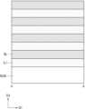
도 15는 본 개시의 일 실시예에 따른 반도체 메모리 소자를 나타낸 사시도이다. 이하에서는 도 2를 참조하여 설명된 반도체 메모리 소자와 도 15를 참조하여 설명되는 반도체 메모리 소자 사이의 차이점이 설명된다.FIG. 15 is a perspective view illustrating a semiconductor memory device according to one embodiment of the present disclosure. Hereinafter, differences between the semiconductor memory device described with reference to FIG. 2 and the semiconductor memory device described with reference to FIG. 15 will be described.
도 15를 참조하면, 각각의 비트 라인(BL)은 수직 방향(D3)으로 연장될 수 있고, 복수의 비트 라인(BL)은 제1 수평 방향(D1)으로 서로 이격될 수 있다. 수직 방향(D3)으로 이격된 복수의 반도체 패턴(SP)의 제1 소스/드레인 영역(SD1)은 동일한 비트 라인(BL)에 전기적으로 연결될 수 있다. 제1 수평 방향(D1)으로 이격된 복수의 반도체 패턴(SP)의 제1 소스/드레인 영역(SD1)은 상이한 복수의 비트 라인(BL)에 각각 전기적으로 연결될 수 있다.Referring to FIG. 15, each bit line (BL) may extend in a vertical direction (D3), and a plurality of bit lines (BL) may be spaced apart from each other in a first horizontal direction (D1). First source/drain regions (SD1) of a plurality of semiconductor patterns (SP) spaced apart in the vertical direction (D3) may be electrically connected to the same bit line (BL). First source/drain regions (SD1) of a plurality of semiconductor patterns (SP) spaced apart in the first horizontal direction (D1) may be electrically connected to different bit lines (BL), respectively.
각각의 워드 라인 구조체(WLS)는 제1 수평 방향(D1)으로 연장될 수 있고, 복수의 워드 라인 구조체(WLS)는 수직 방향(D3)으로 서로 이격될 수 있다. 제1 수평 방향(D1)으로 이격된 복수의 반도체 패턴(SP)은 동일한 워드 라인 구조체(WLS)에 접촉할 수 있다. 워드 라인 구조체(WLS)는 제1 수평 방향(D1)으로 이격된 복수의 반도체 패턴(SP)의 양 측면과 접촉할 수 있다. 수직 방향(D3)으로 서로 이격된 복수의 반도체 패턴(SP)은 상이한 복수의 워드 라인 구조체(WLS)에 각각 접촉할 수 있다.Each word line structure (WLS) can extend in a first horizontal direction (D1), and a plurality of word line structures (WLS) can be spaced apart from each other in a vertical direction (D3). A plurality of semiconductor patterns (SP) spaced apart from each other in the first horizontal direction (D1) can contact the same word line structure (WLS). The word line structure (WLS) can contact both side surfaces of the plurality of semiconductor patterns (SP) spaced apart from each other in the first horizontal direction (D1). A plurality of semiconductor patterns (SP) spaced apart from each other in the vertical direction (D3) can each contact different plurality of word line structures (WLS).
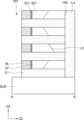
도 16a는 본 개시의 일 실시예에 따른 반도체 메모리 소자를 나타낸 평면도이다. 도 16b는 도 16a의 A-A' 선을 따른 단면도이다. 이하에서는 도 3 및 도 4a 내지 도 4c를 참조하여 설명된 반도체 메모리 소자와 도 16a 및 도 16b를 참조하여 설명되는 반도체 메모리 소자 사이의 차이점이 설명된다.FIG. 16A is a plan view showing a semiconductor memory device according to one embodiment of the present disclosure. FIG. 16B is a cross-sectional view taken along line A-A' of FIG. 16A. Hereinafter, differences between the semiconductor memory device described with reference to FIGS. 3 and 4A to 4C and the semiconductor memory device described with reference to FIGS. 16A and 16B will be described.
도 16a 및 도 16b를 참조하면, 제1 전극(EL)은 상판(P1), 하판(P2), 및 상판(P1)과 하판(P2) 사이에 연장되는 측벽(P3)을 포함할 수 있다. 상판(P1) 및 하판(P2)은 수직 방향(D3)에 수직할 수 있다. 측벽(P3)은 수직 방향(D3)으로 연장될 수 있다. 평면적 관점에서, 상판(P1), 하판(P2), 및 측벽(P3)은 폐루프 형상을 가질 수 있다. 예를 들어, 평면적 관점에서, 상판(P1), 하판(P2), 및 측벽(P3)은 원형일 수 있다.Referring to FIGS. 16A and 16B, the first electrode (EL) may include an upper plate (P1), a lower plate (P2), and a side wall (P3) extending between the upper plate (P1) and the lower plate (P2). The upper plate (P1) and the lower plate (P2) may be perpendicular to the vertical direction (D3). The side wall (P3) may extend in the vertical direction (D3). In a plan view, the upper plate (P1), the lower plate (P2), and the side wall (P3) may have a closed loop shape. For example, in a plan view, the upper plate (P1), the lower plate (P2), and the side wall (P3) may be circular.
일부 실시예에서, 반도체 패턴(SP1)는 측벽(P3)의 둘레 전체를 따라 배치될 수 있다. 즉, 제1 전극(EL1)은 반도체 패턴(SP)을 관통할 수 있다. 반도체 패턴(SP)의 일부는 측벽(P3)과 수직 절연 층(VIP) 사이에 배치될 수 있다.In some embodiments, the semiconductor pattern (SP1) may be arranged along the entire perimeter of the sidewall (P3). That is, the first electrode (EL1) may penetrate the semiconductor pattern (SP). A portion of the semiconductor pattern (SP) may be arranged between the sidewall (P3) and the vertical insulating layer (VIP).
유전 층(DL)은 제1 전극(EL1) 상에 컨포말하게 배치될 수 있다. 제2 전극(EL2)은 유전 층(DL) 상에 배치될 수 있다. 제2 전극(EL2)은 수직 방향(D3)으로 적층된 복수의 제1 전극(EL1)을 관통할 수 있다. 제2 전극(EL2)은 수직 방향(D3)으로 연장되는 기둥 형상을 가질 수 있다. 즉, 제1 전극(EL1)은 제2 전극(EL2)의 둘레를 따라 배치될 수 있다. 단면도적인 관점에서, 제2 전극(EL2)은 수직 방향(D3)으로 연장되는 피쉬 본(fish-bone) 형상을 가질 수 있다.The dielectric layer (DL) can be conformally arranged on the first electrode (EL1). The second electrode (EL2) can be arranged on the dielectric layer (DL). The second electrode (EL2) can penetrate a plurality of first electrodes (EL1) that are stacked in a vertical direction (D3). The second electrode (EL2) can have a pillar shape extending in the vertical direction (D3). That is, the first electrode (EL1) can be arranged along the perimeter of the second electrode (EL2). In a cross-sectional view, the second electrode (EL2) can have a fish-bone shape extending in the vertical direction (D3).
본 개시에 개시된 실시예들은 본 개시의 기술적 사상을 한정하기 위한 것이 아니라 설명하기 위한 것이고, 이러한 실시예에 의하여 본 개시의 기술 사상의 범위가 한정되는 것은 아니다. 본 개시의 보호 범위는 아래의 청구범위에 의하여 해석되어야 하며, 그와 동등한 범위 내에 있는 모든 기술적 사상은 본 개시의 권리범위에 포함되는 것으로 해석되어야 할 것이다.The embodiments disclosed in this disclosure are not intended to limit the technical idea of the present disclosure but to explain it, and the scope of the technical idea of the present disclosure is not limited by these embodiments. The protection scope of the present disclosure should be interpreted by the following claims, and all technical ideas within the equivalent scope should be interpreted as being included in the scope of the rights of the present disclosure.
BL: 비트 라인, WL: 워드 라인, WLS: 워드 라인 구조체, GE: 게이트 전극, GI: 게이트 절연 층, DS: 정보 저장 요소, SP: 반도체 패턴, SD1: 제1 소스/드레인 영역, SD2: 제2 소스/드레인 영역, CH: 채널 영역, ISS: 절연 구조체, EL1: 제1 전극, EL2: 제2 전극, DL: 유전 층, IL1: 제1 절연 층, IL2: 제2 절연 층, IL3: 제3 절연 층, IL4: 제4 절연 층, IL5: 제5 절연 층, PS: 다결정 반도체 층, VIP: 수직 절연 층, SUB: 기판, SC1: 제1 실리사이드 패턴, SC2: 제2 실리사이드 패턴BL: bit line, WL: word line, WLS: word line structure, GE: gate electrode, GI: gate insulating layer, DS: information storage element, SP: semiconductor pattern, SD1: first source/drain region, SD2: second source/drain region, CH: channel region, ISS: insulating structure, EL1: first electrode, EL2: second electrode, DL: dielectric layer, IL1: first insulating layer, IL2: second insulating layer, IL3: third insulating layer, IL4: fourth insulating layer, IL5: fifth insulating layer, PS: polycrystalline semiconductor layer, VIP: vertical insulating layer, SUB: substrate, SC1: first silicide pattern, SC2: second silicide pattern
Claims (10)
Translated fromKorean상기 제1 반도체 패턴 및 상기 제2 반도체 패턴의 제1 소스/드레인 영역들에 각각 전기적으로 연결되는 두 비트 라인;
상기 제1 반도체 패턴 및 상기 제2 반도체 패턴과 접촉하는 워드 라인 구조체; 및
상기 제1 반도체 패턴 및 상기 제2 반도체 패턴의 제2 소스/드레인 영역들에 각각 전기적으로 연결되는 두 정보 저장 요소를 포함하고,
상기 제1 반도체 패턴 및 상기 제2 반도체 패턴은 단결정이고,
상기 제1 반도체 패턴의 결정 방향은 상기 제2 반도체 패턴의 결정 방향과 상이하며,
상기 제1 반도체 패턴 및 상기 제2 반도체 패턴 중 적어도 하나는 상기 적어도 하나의 하면 또는 상면에 대하여 비스듬하게 연장되는 격자 결함을 갖는 것을 특징으로 하는 반도체 메모리 소자.A first semiconductor pattern and a second semiconductor pattern spaced apart from each other in a vertical direction;
Two bit lines electrically connected to first source/drain regions of the first semiconductor pattern and the second semiconductor pattern, respectively;
A word line structure in contact with the first semiconductor pattern and the second semiconductor pattern; and
It comprises two information storage elements electrically connected to the second source/drain regions of the first semiconductor pattern and the second semiconductor pattern, respectively;
The above first semiconductor pattern and the above second semiconductor pattern are single crystals,
The crystal direction of the first semiconductor pattern is different from the crystal direction of the second semiconductor pattern,
A semiconductor memory device characterized in that at least one of the first semiconductor pattern and the second semiconductor pattern has a lattice defect extending obliquely with respect to at least one lower or upper surface.
상기 격자 결함과 상기 제1 반도체 패턴 및 상기 제2 반도체 패턴 중 상기 적어도 하나의 하면 또는 상면 사이의 각도는 50도 내지 60도인 것을 특징으로 하는 반도체 메모리 소자.In the first paragraph,
A semiconductor memory device, characterized in that the angle between the lattice defect and the lower surface or upper surface of at least one of the first semiconductor pattern and the second semiconductor pattern is 50 to 60 degrees.
상기 두 비트 라인 각각은 제1 수평 방향으로 연장되며, 상기 두 비트 라인은 상기 수직 방향으로 서로 이격되는 것을 특징으로 하는 반도체 메모리 소자.In the first paragraph,
A semiconductor memory device, characterized in that each of the two bit lines extends in a first horizontal direction, and the two bit lines are spaced apart from each other in the vertical direction.
상기 워드 라인 구조체는 상기 수직 방향으로 연장되는 것을 특징으로 하는 반도체 메모리 소자.In the first paragraph,
A semiconductor memory device characterized in that the word line structure extends in the vertical direction.
상기 복수의 반도체 패턴의 제1 소스/드레인 영역들에 전기적으로 연결되는 비트 라인;
상기 복수의 반도체 패턴과 각각 접촉하는 복수의 워드 라인 구조체; 및
상기 복수의 반도체 패턴의 제2 소스/드레인 영역들에 각각 전기적으로 연결되는 복수의 정보 저장 요소를 포함하고,
상기 복수의 반도체 패턴은 단결정이고,
상기 복수의 반도체 패턴 중 적어도 하나의 결정 방향은 상기 복수의 반도체 패턴 중 다른 하나의 결정 방향과 상이하며,
상기 복수의 반도체 패턴 중 적어도 하나는 상기 적어도 하나의 하면 또는 상면에 대하여 비스듬하게 연장되는 격자 결함을 갖는 것을 특징으로 하는 반도체 메모리 소자.A plurality of semiconductor patterns spaced vertically from each other;
A bit line electrically connected to the first source/drain regions of the plurality of semiconductor patterns;
A plurality of word line structures each in contact with the plurality of semiconductor patterns; and
A plurality of information storage elements each electrically connected to the second source/drain regions of the plurality of semiconductor patterns,
The above plurality of semiconductor patterns are single crystals,
The crystal direction of at least one of the plurality of semiconductor patterns is different from the crystal direction of another one of the plurality of semiconductor patterns,
A semiconductor memory device characterized in that at least one of the plurality of semiconductor patterns has a lattice defect extending obliquely with respect to at least one lower or upper surface.
상기 비트 라인은 상기 수직 방향으로 연장되는 것을 특징으로 하는 반도체 메모리 소자.In Article 6,
A semiconductor memory device characterized in that the bit line extends in the vertical direction.
상기 복수의 워드 라인 구조체 각각은 제1 수평 방향으로 연장되고,
상기 복수의 워드 라인 구조체는 상기 수직 방향으로 서로 이격되는 것을 특징으로 하는 반도체 메모리 소자.In Article 6,
Each of the plurality of word line structures extends in a first horizontal direction,
A semiconductor memory device, characterized in that the plurality of word line structures are spaced apart from each other in the vertical direction.
상기 복수의 반도체 패턴을 상기 수직 방향으로 이격시키는 복수의 절연 층;
상기 복수의 반도체 패턴 중 몇몇의 제1 소스/드레인 영역들에 전기적으로 연결되는 비트 라인;
상기 복수의 반도체 패턴 중 몇몇과 접촉하는 워드 라인 구조체; 및
상기 복수의 반도체 패턴의 제2 소스/드레인 영역들에 각각 전기적으로 연결되는 복수의 정보 저장 요소를 포함하고,
상기 복수의 반도체 패턴은 단결정이고,
상기 복수의 반도체 패턴 중 적어도 하나의 결정 방향은 상기 복수의 반도체 패턴 중 다른 하나의 결정 방향과 상이하며,
상기 복수의 반도체 패턴 중 적어도 하나는 상기 적어도 하나의 하면 또는 상면에 대하여 비스듬하게 연장되는 격자 결함을 갖는 것을 특징으로 하는 반도체 메모리 소자.A plurality of semiconductor patterns arranged two-dimensionally in a vertical direction and a first horizontal direction, each extending in a second horizontal direction;
A plurality of insulating layers that space the plurality of semiconductor patterns apart in the vertical direction;
A bit line electrically connected to some of the first source/drain regions of the plurality of semiconductor patterns;
a word line structure in contact with some of the plurality of semiconductor patterns; and
A plurality of information storage elements each electrically connected to the second source/drain regions of the plurality of semiconductor patterns,
The above plurality of semiconductor patterns are single crystals,
The crystal direction of at least one of the plurality of semiconductor patterns is different from the crystal direction of another one of the plurality of semiconductor patterns,
A semiconductor memory device characterized in that at least one of the plurality of semiconductor patterns has a lattice defect extending obliquely with respect to at least one lower or upper surface.
상기 복수의 반도체 패턴은 제1 반도체 패턴을 포함하고,
상기 복수의 절연 층은 상기 제1 반도체 패턴의 상면 상의 상부 절연 층, 및 상기 반도체 패턴의 하면 상의 하부 절연 층을 포함하고,
상기 제1 반도체 패턴은 상기 상부 절연 층의 하면 및 상기 하부 절연 층의 상면 중 적어도 하나에 대하여 비스듬하게 연장되는 상기 격자 결함을 가지는 것을 특징으로 하는 반도체 메모리 소자.In Article 9,
The above plurality of semiconductor patterns include a first semiconductor pattern,
The above plurality of insulating layers include an upper insulating layer on the upper surface of the first semiconductor pattern, and a lower insulating layer on the lower surface of the semiconductor pattern,
A semiconductor memory device characterized in that the first semiconductor pattern has the lattice defect extending obliquely with respect to at least one of the lower surface of the upper insulating layer and the upper surface of the lower insulating layer.
Priority Applications (4)
| Application Number | Priority Date | Filing Date | Title |
|---|---|---|---|
| KR1020200098193AKR102757508B1 (en) | 2020-08-05 | 2020-08-05 | Semiconductor memory device |
| US17/193,739US11700723B2 (en) | 2020-08-05 | 2021-03-05 | Semiconductor memory device |
| CN202110339130.8ACN114068568A (en) | 2020-08-05 | 2021-03-30 | semiconductor memory device |
| TW110115024ATWI798688B (en) | 2020-08-05 | 2021-04-27 | Semiconductor memory device |
Applications Claiming Priority (1)
| Application Number | Priority Date | Filing Date | Title |
|---|---|---|---|
| KR1020200098193AKR102757508B1 (en) | 2020-08-05 | 2020-08-05 | Semiconductor memory device |
Publications (2)
| Publication Number | Publication Date |
|---|---|
| KR20220017774A KR20220017774A (en) | 2022-02-14 |
| KR102757508B1true KR102757508B1 (en) | 2025-01-20 |
Family
ID=80115282
Family Applications (1)
| Application Number | Title | Priority Date | Filing Date |
|---|---|---|---|
| KR1020200098193AActiveKR102757508B1 (en) | 2020-08-05 | 2020-08-05 | Semiconductor memory device |
Country Status (4)
| Country | Link |
|---|---|
| US (1) | US11700723B2 (en) |
| KR (1) | KR102757508B1 (en) |
| CN (1) | CN114068568A (en) |
| TW (1) | TWI798688B (en) |
Families Citing this family (7)
| Publication number | Priority date | Publication date | Assignee | Title |
|---|---|---|---|---|
| US12225718B2 (en) | 2022-04-21 | 2025-02-11 | Changxin Memory Technologies, Inc. | Semiconductor structure and method for forming semiconductor structure |
| CN116997176A (en)* | 2022-04-21 | 2023-11-03 | 长鑫存储技术有限公司 | Semiconductor structure and forming method thereof |
| KR102772517B1 (en)* | 2022-04-28 | 2025-02-26 | 한양대학교 산학협력단 | 3d memory array and manufacturing method thereof |
| CN115064494A (en)* | 2022-06-08 | 2022-09-16 | 长鑫存储技术有限公司 | Semiconductor structure and preparation method |
| CN117352489A (en) | 2022-06-21 | 2024-01-05 | 长鑫存储技术有限公司 | Semiconductor structure, manufacturing method thereof, memory chip and electronic equipment |
| CN117352490A (en)* | 2022-06-21 | 2024-01-05 | 长鑫存储技术有限公司 | Semiconductor structure, manufacturing method thereof, memory chip and electronic equipment |
| EP4475164A4 (en)* | 2022-06-22 | 2025-06-11 | Changxin Memory Technologies, Inc. | Semiconductor structure and manufacturing method therefor |
Family Cites Families (14)
| Publication number | Priority date | Publication date | Assignee | Title |
|---|---|---|---|---|
| KR100497672B1 (en) | 2002-05-10 | 2005-07-01 | 재단법인서울대학교산학협력재단 | Dram using aligned soi double gate transistor and process thereof |
| EP1993130A3 (en)* | 2007-05-17 | 2011-09-07 | Semiconductor Energy Laboratory Co., Ltd. | Semiconductor device and method for manufacturing the same |
| FR2928028B1 (en) | 2008-02-27 | 2011-07-15 | St Microelectronics Crolles 2 | METHOD FOR MANUFACTURING A BENT GRID SEMICONDUCTOR DEVICE AND CORRESPONDING INTEGRATED CIRCUIT |
| KR20100097468A (en) | 2009-02-26 | 2010-09-03 | 삼성전자주식회사 | Semiconductor memory device and method of manufacturing the same |
| US9953870B2 (en) | 2011-06-28 | 2018-04-24 | Monolithic 3D Inc. | 3D semiconductor device and system |
| US8441053B2 (en) | 2010-10-15 | 2013-05-14 | Powerchip Technology Corporation | Vertical capacitor-less DRAM cell, DRAM array and operation of the same |
| US9576788B2 (en) | 2015-04-24 | 2017-02-21 | Applied Materials, Inc. | Cleaning high aspect ratio vias |
| KR102600110B1 (en)* | 2017-09-29 | 2023-11-10 | 삼성전자주식회사 | Semiconductor memory device |
| US10535659B2 (en)* | 2017-09-29 | 2020-01-14 | Samsung Electronics Co., Ltd. | Semiconductor memory devices |
| CN110010620B (en) | 2017-11-21 | 2021-04-13 | 长江存储科技有限责任公司 | Manufacturing method of 3D NAND flash memory with high stack number and 3D NAND flash memory |
| KR102524614B1 (en)* | 2017-11-24 | 2023-04-24 | 삼성전자주식회사 | Semiconductor memory device |
| US10439049B2 (en) | 2017-12-19 | 2019-10-08 | International Business Machines Corporation | Nanosheet device with close source drain proximity |
| WO2020077185A1 (en) | 2018-10-13 | 2020-04-16 | Applied Materials, Inc. | Stacked transistor device |
| US11107733B2 (en)* | 2019-08-06 | 2021-08-31 | Tokyo Electron Limited | Multi-dimensional planes of logic and memory formation using single crystal silicon orientations |
- 2020
- 2020-08-05KRKR1020200098193Apatent/KR102757508B1/enactiveActive
- 2021
- 2021-03-05USUS17/193,739patent/US11700723B2/enactiveActive
- 2021-03-30CNCN202110339130.8Apatent/CN114068568A/enactivePending
- 2021-04-27TWTW110115024Apatent/TWI798688B/enactive
Also Published As
| Publication number | Publication date |
|---|---|
| KR20220017774A (en) | 2022-02-14 |
| US11700723B2 (en) | 2023-07-11 |
| CN114068568A (en) | 2022-02-18 |
| US20220045064A1 (en) | 2022-02-10 |
| TWI798688B (en) | 2023-04-11 |
| TW202221895A (en) | 2022-06-01 |
Similar Documents
| Publication | Publication Date | Title |
|---|---|---|
| KR102757508B1 (en) | Semiconductor memory device | |
| KR102847704B1 (en) | Semiconductor memory device and method for manufacturing the same | |
| US11895852B2 (en) | Method for forming semiconductor structure by using sacrificial layer configured to be replaced subsequently to form bit line, semiconductor structure, and memory | |
| KR102753881B1 (en) | Semiconductor memory device and method for manufacturing the same | |
| KR102816109B1 (en) | Semiconductor device and method of forming the same | |
| US12278285B2 (en) | Semiconductor devices | |
| KR102741647B1 (en) | Semiconductor device | |
| US11239249B2 (en) | Vertical-type memory device | |
| KR20220017554A (en) | Semiconductor device | |
| KR20240000949A (en) | Semiconductor device and method for manufacturing the same | |
| US12408379B2 (en) | Semiconductor device and method of fabricating the same | |
| EP4517830A1 (en) | Semiconductor device and method of fabricating the same | |
| EP4307386A1 (en) | Semiconductor device | |
| TW202407891A (en) | Semiconductor device | |
| US20250006817A1 (en) | Semiconductor devices | |
| US20250107185A1 (en) | Semiconductor devices and methods of manufacturing the same | |
| US20240064999A1 (en) | Semiconductor device including data storage structure and method of manufacturing data storage structure | |
| KR20230063231A (en) | Semiconductor device | |
| TW202501787A (en) | Semiconductor device | |
| KR20250149344A (en) | Semiconductor device | |
| KR20230161174A (en) | Semiconductor device | |
| TW202249183A (en) | Semiconductor device | |
| KR20240044227A (en) | Semiconductor device | |
| KR20240028059A (en) | Semiconductor device | |
| KR20240151435A (en) | Semiconductor device and method for manufacturing the same |
Legal Events
| Date | Code | Title | Description |
|---|---|---|---|
| PA0109 | Patent application | Patent event code:PA01091R01D Comment text:Patent Application Patent event date:20200805 | |
| PG1501 | Laying open of application | ||
| E902 | Notification of reason for refusal | ||
| PE0902 | Notice of grounds for rejection | Comment text:Notification of reason for refusal Patent event date:20240715 Patent event code:PE09021S01D | |
| E701 | Decision to grant or registration of patent right | ||
| PE0701 | Decision of registration | Patent event code:PE07011S01D Comment text:Decision to Grant Registration Patent event date:20241203 | |
| GRNT | Written decision to grant | ||
| PR0701 | Registration of establishment | Comment text:Registration of Establishment Patent event date:20250115 Patent event code:PR07011E01D | |
| PR1002 | Payment of registration fee | Payment date:20250116 End annual number:3 Start annual number:1 | |
| PG1601 | Publication of registration |