KR102756389B1 - Photo transistor and display device comprising of the same - Google Patents
Photo transistor and display device comprising of the sameDownload PDFInfo
- Publication number
- KR102756389B1 KR102756389B1KR1020190174429AKR20190174429AKR102756389B1KR 102756389 B1KR102756389 B1KR 102756389B1KR 1020190174429 AKR1020190174429 AKR 1020190174429AKR 20190174429 AKR20190174429 AKR 20190174429AKR 102756389 B1KR102756389 B1KR 102756389B1
- Authority
- KR
- South Korea
- Prior art keywords
- active layer
- electrode
- layer
- light
- phototransistor
- Prior art date
- Legal status (The legal status is an assumption and is not a legal conclusion. Google has not performed a legal analysis and makes no representation as to the accuracy of the status listed.)
- Active
Links
Images


Classifications
- H—ELECTRICITY
- H10—SEMICONDUCTOR DEVICES; ELECTRIC SOLID-STATE DEVICES NOT OTHERWISE PROVIDED FOR
- H10F—INORGANIC SEMICONDUCTOR DEVICES SENSITIVE TO INFRARED RADIATION, LIGHT, ELECTROMAGNETIC RADIATION OF SHORTER WAVELENGTH OR CORPUSCULAR RADIATION
- H10F30/00—Individual radiation-sensitive semiconductor devices in which radiation controls the flow of current through the devices, e.g. photodetectors
- H10F30/20—Individual radiation-sensitive semiconductor devices in which radiation controls the flow of current through the devices, e.g. photodetectors the devices having potential barriers, e.g. phototransistors
- H10F30/21—Individual radiation-sensitive semiconductor devices in which radiation controls the flow of current through the devices, e.g. photodetectors the devices having potential barriers, e.g. phototransistors the devices being sensitive to infrared, visible or ultraviolet radiation
- H10F30/28—Individual radiation-sensitive semiconductor devices in which radiation controls the flow of current through the devices, e.g. photodetectors the devices having potential barriers, e.g. phototransistors the devices being sensitive to infrared, visible or ultraviolet radiation the devices being characterised by field-effect operation, e.g. junction field-effect phototransistors
- H10F30/2823—Individual radiation-sensitive semiconductor devices in which radiation controls the flow of current through the devices, e.g. photodetectors the devices having potential barriers, e.g. phototransistors the devices being sensitive to infrared, visible or ultraviolet radiation the devices being characterised by field-effect operation, e.g. junction field-effect phototransistors the devices being conductor-insulator-semiconductor devices, e.g. diodes or charge-coupled devices [CCD]
- H—ELECTRICITY
- H10—SEMICONDUCTOR DEVICES; ELECTRIC SOLID-STATE DEVICES NOT OTHERWISE PROVIDED FOR
- H10D—INORGANIC ELECTRIC SEMICONDUCTOR DEVICES
- H10D86/00—Integrated devices formed in or on insulating or conducting substrates, e.g. formed in silicon-on-insulator [SOI] substrates or on stainless steel or glass substrates
- H10D86/40—Integrated devices formed in or on insulating or conducting substrates, e.g. formed in silicon-on-insulator [SOI] substrates or on stainless steel or glass substrates characterised by multiple TFTs
- H—ELECTRICITY
- H10—SEMICONDUCTOR DEVICES; ELECTRIC SOLID-STATE DEVICES NOT OTHERWISE PROVIDED FOR
- H10F—INORGANIC SEMICONDUCTOR DEVICES SENSITIVE TO INFRARED RADIATION, LIGHT, ELECTROMAGNETIC RADIATION OF SHORTER WAVELENGTH OR CORPUSCULAR RADIATION
- H10F10/00—Individual photovoltaic cells, e.g. solar cells
- H10F10/10—Individual photovoltaic cells, e.g. solar cells having potential barriers
- H10F10/16—Photovoltaic cells having only PN heterojunction potential barriers
- H—ELECTRICITY
- H10—SEMICONDUCTOR DEVICES; ELECTRIC SOLID-STATE DEVICES NOT OTHERWISE PROVIDED FOR
- H10F—INORGANIC SEMICONDUCTOR DEVICES SENSITIVE TO INFRARED RADIATION, LIGHT, ELECTROMAGNETIC RADIATION OF SHORTER WAVELENGTH OR CORPUSCULAR RADIATION
- H10F30/00—Individual radiation-sensitive semiconductor devices in which radiation controls the flow of current through the devices, e.g. photodetectors
- H10F30/20—Individual radiation-sensitive semiconductor devices in which radiation controls the flow of current through the devices, e.g. photodetectors the devices having potential barriers, e.g. phototransistors
- H10F30/21—Individual radiation-sensitive semiconductor devices in which radiation controls the flow of current through the devices, e.g. photodetectors the devices having potential barriers, e.g. phototransistors the devices being sensitive to infrared, visible or ultraviolet radiation
- H10F30/28—Individual radiation-sensitive semiconductor devices in which radiation controls the flow of current through the devices, e.g. photodetectors the devices having potential barriers, e.g. phototransistors the devices being sensitive to infrared, visible or ultraviolet radiation the devices being characterised by field-effect operation, e.g. junction field-effect phototransistors
- H10F30/282—Insulated-gate field-effect transistors [IGFET], e.g. MISFET [metal-insulator-semiconductor field-effect transistor] phototransistors
- H—ELECTRICITY
- H10—SEMICONDUCTOR DEVICES; ELECTRIC SOLID-STATE DEVICES NOT OTHERWISE PROVIDED FOR
- H10F—INORGANIC SEMICONDUCTOR DEVICES SENSITIVE TO INFRARED RADIATION, LIGHT, ELECTROMAGNETIC RADIATION OF SHORTER WAVELENGTH OR CORPUSCULAR RADIATION
- H10F77/00—Constructional details of devices covered by this subclass
- H10F77/10—Semiconductor bodies
- H10F77/12—Active materials
- H10F77/126—Active materials comprising only Group I-III-VI chalcopyrite materials, e.g. CuInSe2, CuGaSe2 or CuInGaSe2 [CIGS]
- H—ELECTRICITY
- H10—SEMICONDUCTOR DEVICES; ELECTRIC SOLID-STATE DEVICES NOT OTHERWISE PROVIDED FOR
- H10F—INORGANIC SEMICONDUCTOR DEVICES SENSITIVE TO INFRARED RADIATION, LIGHT, ELECTROMAGNETIC RADIATION OF SHORTER WAVELENGTH OR CORPUSCULAR RADIATION
- H10F77/00—Constructional details of devices covered by this subclass
- H10F77/10—Semiconductor bodies
- H10F77/16—Material structures, e.g. crystalline structures, film structures or crystal plane orientations
- H10F77/162—Non-monocrystalline materials, e.g. semiconductor particles embedded in insulating materials
- H10F77/164—Polycrystalline semiconductors
- H10F77/1642—Polycrystalline semiconductors including only Group IV materials
- H—ELECTRICITY
- H10—SEMICONDUCTOR DEVICES; ELECTRIC SOLID-STATE DEVICES NOT OTHERWISE PROVIDED FOR
- H10F—INORGANIC SEMICONDUCTOR DEVICES SENSITIVE TO INFRARED RADIATION, LIGHT, ELECTROMAGNETIC RADIATION OF SHORTER WAVELENGTH OR CORPUSCULAR RADIATION
- H10F77/00—Constructional details of devices covered by this subclass
- H10F77/10—Semiconductor bodies
- H10F77/16—Material structures, e.g. crystalline structures, film structures or crystal plane orientations
- H10F77/162—Non-monocrystalline materials, e.g. semiconductor particles embedded in insulating materials
- H10F77/166—Amorphous semiconductors
- H10F77/1662—Amorphous semiconductors including only Group IV materials
- H—ELECTRICITY
- H10—SEMICONDUCTOR DEVICES; ELECTRIC SOLID-STATE DEVICES NOT OTHERWISE PROVIDED FOR
- H10K—ORGANIC ELECTRIC SOLID-STATE DEVICES
- H10K10/00—Organic devices specially adapted for rectifying, amplifying, oscillating or switching; Organic capacitors or resistors having potential barriers
- H10K10/40—Organic transistors
- H10K10/46—Field-effect transistors, e.g. organic thin-film transistors [OTFT]
- H10K10/462—Insulated gate field-effect transistors [IGFETs]
- H10K10/484—Insulated gate field-effect transistors [IGFETs] characterised by the channel regions
- H—ELECTRICITY
- H10—SEMICONDUCTOR DEVICES; ELECTRIC SOLID-STATE DEVICES NOT OTHERWISE PROVIDED FOR
- H10K—ORGANIC ELECTRIC SOLID-STATE DEVICES
- H10K50/00—Organic light-emitting devices
- H10K50/80—Constructional details
- H10K50/84—Passivation; Containers; Encapsulations
- H10K50/844—Encapsulations
- H—ELECTRICITY
- H10—SEMICONDUCTOR DEVICES; ELECTRIC SOLID-STATE DEVICES NOT OTHERWISE PROVIDED FOR
- H10K—ORGANIC ELECTRIC SOLID-STATE DEVICES
- H10K59/00—Integrated devices, or assemblies of multiple devices, comprising at least one organic light-emitting element covered by group H10K50/00
- H10K59/40—OLEDs integrated with touch screens
- H—ELECTRICITY
- H10—SEMICONDUCTOR DEVICES; ELECTRIC SOLID-STATE DEVICES NOT OTHERWISE PROVIDED FOR
- H10K—ORGANIC ELECTRIC SOLID-STATE DEVICES
- H10K59/00—Integrated devices, or assemblies of multiple devices, comprising at least one organic light-emitting element covered by group H10K50/00
- H10K59/60—OLEDs integrated with inorganic light-sensitive elements, e.g. with inorganic solar cells or inorganic photodiodes
- H—ELECTRICITY
- H10—SEMICONDUCTOR DEVICES; ELECTRIC SOLID-STATE DEVICES NOT OTHERWISE PROVIDED FOR
- H10K—ORGANIC ELECTRIC SOLID-STATE DEVICES
- H10K59/00—Integrated devices, or assemblies of multiple devices, comprising at least one organic light-emitting element covered by group H10K50/00
- H10K59/80—Constructional details
- H10K59/87—Passivation; Containers; Encapsulations
- H10K59/873—Encapsulations
- G—PHYSICS
- G06—COMPUTING OR CALCULATING; COUNTING
- G06F—ELECTRIC DIGITAL DATA PROCESSING
- G06F3/00—Input arrangements for transferring data to be processed into a form capable of being handled by the computer; Output arrangements for transferring data from processing unit to output unit, e.g. interface arrangements
- G06F3/01—Input arrangements or combined input and output arrangements for interaction between user and computer
- G06F3/03—Arrangements for converting the position or the displacement of a member into a coded form
- G06F3/041—Digitisers, e.g. for touch screens or touch pads, characterised by the transducing means
- G06F3/0412—Digitisers structurally integrated in a display
- H—ELECTRICITY
- H10—SEMICONDUCTOR DEVICES; ELECTRIC SOLID-STATE DEVICES NOT OTHERWISE PROVIDED FOR
- H10K—ORGANIC ELECTRIC SOLID-STATE DEVICES
- H10K50/00—Organic light-emitting devices
- H10K50/10—OLEDs or polymer light-emitting diodes [PLED]
- H10K50/11—OLEDs or polymer light-emitting diodes [PLED] characterised by the electroluminescent [EL] layers
- H—ELECTRICITY
- H10—SEMICONDUCTOR DEVICES; ELECTRIC SOLID-STATE DEVICES NOT OTHERWISE PROVIDED FOR
- H10K—ORGANIC ELECTRIC SOLID-STATE DEVICES
- H10K59/00—Integrated devices, or assemblies of multiple devices, comprising at least one organic light-emitting element covered by group H10K50/00
- H10K59/10—OLED displays
- H10K59/12—Active-matrix OLED [AMOLED] displays
- Y—GENERAL TAGGING OF NEW TECHNOLOGICAL DEVELOPMENTS; GENERAL TAGGING OF CROSS-SECTIONAL TECHNOLOGIES SPANNING OVER SEVERAL SECTIONS OF THE IPC; TECHNICAL SUBJECTS COVERED BY FORMER USPC CROSS-REFERENCE ART COLLECTIONS [XRACs] AND DIGESTS
- Y02—TECHNOLOGIES OR APPLICATIONS FOR MITIGATION OR ADAPTATION AGAINST CLIMATE CHANGE
- Y02E—REDUCTION OF GREENHOUSE GAS [GHG] EMISSIONS, RELATED TO ENERGY GENERATION, TRANSMISSION OR DISTRIBUTION
- Y02E10/00—Energy generation through renewable energy sources
- Y02E10/50—Photovoltaic [PV] energy
- Y02E10/541—CuInSe2 material PV cells
Landscapes
- Life Sciences & Earth Sciences (AREA)
- Chemical & Material Sciences (AREA)
- Inorganic Chemistry (AREA)
- Sustainable Development (AREA)
- Physics & Mathematics (AREA)
- Optics & Photonics (AREA)
- Engineering & Computer Science (AREA)
- Thin Film Transistor (AREA)
- General Engineering & Computer Science (AREA)
- Theoretical Computer Science (AREA)
- Microelectronics & Electronic Packaging (AREA)
- Human Computer Interaction (AREA)
- General Physics & Mathematics (AREA)
- Devices For Indicating Variable Information By Combining Individual Elements (AREA)
Abstract
Translated fromKoreanDescription
Translated fromKorean본 발명은 포토 트랜지스터 및 이를 포함하는 표시 장치에 관한 것이다.The present invention relates to a phototransistor and a display device including the same.
포토 트랜지스터는 빛 에너지를 전기 에너지로 변환하는 광 센서의 한 종류로서, 빛의 세기에 따라 흐르는 전류가 변화하는 광기전력 효과를 이용한다. 포토 트랜지스터는 트랜지스터를 이용하여 광 전류를 증폭시킬 수 있어 포토 다이오드에 비해 빛에 더 민감한 장점이 있다.A phototransistor is a type of light sensor that converts light energy into electrical energy, using the photovoltaic effect, in which the current flowing changes depending on the intensity of light. A phototransistor has the advantage of being more sensitive to light than a photodiode because it can amplify light current using a transistor.
산화물 반도체는 비정질 실리콘에 비해서 높은 이동도, 투명성, 저온 공정 등 다양한 장점을 가지고 있어 최근에는 산화물 반도체를 포토 트랜지스터에 활용하고자 하는 노력들이 계속되고 있다.Oxide semiconductors have various advantages over amorphous silicon, such as high mobility, transparency, and low-temperature processing, and efforts are being made to utilize oxide semiconductors in phototransistors.
본 발명이 해결하고자 하는 과제는 가시광선 대역의 광 흡수율을 향상시킬 수 있는 포토 트랜지스터를 제공하는 것이다.The problem to be solved by the present invention is to provide a phototransistor capable of improving light absorption in the visible light band.
또한, 본 발명이 해결하고자 하는 과제는 포토 트랜지스터를 광센서로 구비하는 표시 장치를 제공하는 것이다.In addition, the problem that the present invention seeks to solve is to provide a display device having a phototransistor as a light sensor.
본 발명의 과제들은 이상에서 언급한 과제로 제한되지 않으며, 언급되지 않은 또 다른 기술적 과제들은 아래의 기재로부터 당업자에게 명확하게 이해될 수 있을 것이다.The tasks of the present invention are not limited to the tasks mentioned above, and other technical tasks not mentioned will be clearly understood by those skilled in the art from the description below.
상기 과제를 해결하기 위한 일 실시예에 따른 포토 트랜지스터는 기판 상에 배치된 게이트 전극, 상기 게이트 전극을 절연시키는 게이트 절연막, 상기 게이트 절연막을 사이에 두고 상기 게이트 전극과 중첩하며, 금속 산화물을 포함하는 제1 활성층, 상기 제1 활성층 상에 배치되며, 셀레늄을 포함하는 제2 활성층, 및 상기 제2 활성층에 각각 연결되는 소스 전극 및 드레인 전극을 포함할 수 있다.According to one embodiment of the present invention for solving the above problem, a phototransistor may include a gate electrode disposed on a substrate, a gate insulating film insulating the gate electrode, a first active layer overlapping the gate electrode with the gate insulating film interposed therebetween and including a metal oxide, a second active layer disposed on the first active layer and including selenium, and a source electrode and a drain electrode each connected to the second active layer.
상기 제1 활성층과 상기 제2 활성층은 상기 게이트 전극과 중첩하는 영역에서 서로 접할 수 있다.The first active layer and the second active layer can contact each other in a region overlapping the gate electrode.
상기 제1 활성층은 상기 제2 활성층보다 상기 게이트 전극에 인접하여 배치될 수 있다.The first active layer may be arranged closer to the gate electrode than the second active layer.
상기 소스 전극은 상기 제2 활성층의 일부를 덮고, 상기 드레인 전극은 상기 제2 활성층의 다른 일부를 덮을 수 있다.The source electrode may cover a portion of the second active layer, and the drain electrode may cover another portion of the second active layer.
상기 제1 활성층의 측벽과 상기 제2 활성층의 측벽은 서로 접하여 상호 정렬될 수 있다.The side walls of the first active layer and the side walls of the second active layer can be in contact with each other and aligned with each other.
상기 소스 전극 및 상기 드레인 전극 각각은 상기 제1 활성층과 상기 제2 활성층 사이에 배치될 수 있다.Each of the source electrode and the drain electrode can be positioned between the first active layer and the second active layer.
상기 제1 활성층은 산화물 반도체, 비정질 실리콘, 다결정 실리콘 또는 2D 물질(2 dimensional material)을 포함할 수 있다.The first active layer may include an oxide semiconductor, amorphous silicon, polycrystalline silicon, or a 2-dimensional material.
상기 산화물 반도체는 인듐(In), 아연(Zn), 갈륨(Ga), 주석(Sn), 티타늄(Ti), 알루미늄(Al), 하프늄(Hf), 지르코늄(Zr) 또는 마그네슘(Mg) 중 어느 하나 이상을 포함하는 화합물을 포함하며, 상기 2D 물질은 그래핀(graphene) 또는 MoS를 포함할 수 있다.The above oxide semiconductor includes a compound including at least one of indium (In), zinc (Zn), gallium (Ga), tin (Sn), titanium (Ti), aluminum (Al), hafnium (Hf), zirconium (Zr), and magnesium (Mg), and the 2D material may include graphene or MoS.
상기 제2 활성층은 적어도 셀레늄을 포함하며, 구리(Cu), 인듐(In) 또는 갈륨(Ga) 중 어느 하나 이상을 포함하는 화합물을 포함할 수 있다.The second active layer may include a compound including at least selenium and at least one of copper (Cu), indium (In), or gallium (Ga).
상기 제2 활성층의 두께는 5 내지 300nm일 수 있다.The thickness of the second active layer may be 5 to 300 nm.
또한, 일 실시예에 따른 표시 장치는 투과 영역 및 발광 영역을 포함하는 기판, 상기 기판 상에 배치되며, 제1 트랜지스터 및 제2 트랜지스터를 포함하는 트랜지스터층, 상기 트랜지스터층 상에 배치되며, 적어도 제1 전극을 포함하는 발광 소자층, 및 상기 발광 소자층 상에 배치되며, 복수의 전극들을 포함하는 터치 센싱 유닛을 포함하며, 상기 제1 트랜지스터는 게이트 전극, 금속 산화물을 포함하는 제1 활성층, 셀레늄을 포함하는 제2 활성층, 및 소스 전극과 드레인 전극을 포함할 수 있다.In addition, a display device according to one embodiment includes a substrate including a transparent region and a light-emitting region, a transistor layer disposed on the substrate and including a first transistor and a second transistor, a light-emitting element layer disposed on the transistor layer and including at least a first electrode, and a touch sensing unit disposed on the light-emitting element layer and including a plurality of electrodes, wherein the first transistor may include a gate electrode, a first active layer including a metal oxide, a second active layer including selenium, and a source electrode and a drain electrode.
상기 제1 트랜지스터는 상기 기판의 상기 투과 영역과 중첩하고, 상기 제2 트랜지스터는 상기 발광 영역과 중첩할 수 있다.The first transistor may overlap the transmitting region of the substrate, and the second transistor may overlap the emitting region.
상기 제1 트랜지스터는 상기 발광 소자층의 상기 제1 전극과 비중첩하고, 상기 터치 센싱 유닛의 상기 복수의 전극들과 비중첩할 수 있다.The first transistor may be non-overlapping with the first electrode of the light-emitting element layer and non-overlapping with the plurality of electrodes of the touch sensing unit.
상기 제2 트랜지스터는 상기 발광 소자층의 상기 제1 전극과 중첩하고, 상기 터치 센싱 유닛의 상기 복수의 전극들과 비중첩할 수 있다.The second transistor may overlap with the first electrode of the light-emitting element layer and may not overlap with the plurality of electrodes of the touch sensing unit.
상기 발광 소자층은 상기 제1 전극, 상기 제1 전극과 대향하는 제2 전극, 및 상기 제1 전극과 상기 제2 전극 사이에 개재된 유기 발광층을 더 포함하며, 상기 제1 트랜지스터 및 상기 제2 트랜지스터는 상기 제2 전극과 중첩할 수 있다.The light emitting element layer further includes the first electrode, a second electrode opposing the first electrode, and an organic light emitting layer interposed between the first electrode and the second electrode, and the first transistor and the second transistor can overlap the second electrode.
상기 발광 소자층과 상기 터치 센싱 유닛 사이에 배치된 박막 봉지층을 더 포함할 수 있다.It may further include a thin film encapsulation layer disposed between the light emitting element layer and the touch sensing unit.
상기 터치 센싱 유닛의 상기 복수의 전극들은 구동 전극들과 감지 전극들을 포함할 수 있다.The plurality of electrodes of the above touch sensing unit may include driving electrodes and sensing electrodes.
상기 제1 활성층과 상기 제2 활성층은 상기 게이트 전극과 중첩하는 영역에서 서로 접할 수 있다.The first active layer and the second active layer can contact each other in a region overlapping the gate electrode.
상기 제1 활성층은 상기 제2 활성층보다 상기 게이트 전극에 인접하여 배치될 수 있다.The first active layer may be arranged closer to the gate electrode than the second active layer.
상기 제2 활성층은 적어도 셀레늄을 포함하며, 구리(Cu), 인듐(In) 또는 갈륨(Ga) 중 어느 하나 이상을 포함하는 화합물을 포함할 수 있다.The second active layer may include a compound including at least selenium and at least one of copper (Cu), indium (In), or gallium (Ga).
기타 실시예의 구체적인 사항들은 상세한 설명 및 도면들에 포함되어 있다.Specific details of other embodiments are included in the detailed description and drawings.
일 실시예에 따른 포토 트랜지스터에 의하면, 금속 산화물을 포함하는 제1 활성층에 더해 셀레늄을 포함하는 제2 활성층을 포함함으로써, 가시광 파장대 전체의 빛을 흡수함으로써, 광 센싱 특성을 향상시킬 수 있다. 또한, 포토 트랜지스터의 광 응답률, 광민감도 및 검출율을 향상시킬 수 있다.According to a phototransistor according to one embodiment, by including a second active layer including selenium in addition to a first active layer including a metal oxide, light sensing characteristics can be improved by absorbing light in the entire visible light wavelength range. In addition, the optical response rate, optical sensitivity, and detectivity of the phototransistor can be improved.
또한, 일 실시예에 따른 표시 장치에 의하면, 특성이 우수한 포토 트랜지스터를 구비함으로써, 표시 장치의 광 센싱 특성을 향상시킬 수 있다.In addition, according to the display device according to one embodiment, by providing a phototransistor having excellent characteristics, the light sensing characteristics of the display device can be improved.
실시예들에 따른 효과는 이상에서 예시된 내용에 의해 제한되지 않으며, 더욱 다양한 효과들이 본 명세서 내에 포함되어 있다.The effects according to the embodiments are not limited to the contents exemplified above, and more diverse effects are included in the present specification.
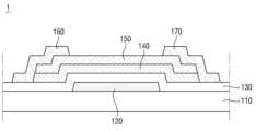
도 1은 일 실시예에 따른 포토 트랜지스터를 나타낸 사시도.
도 2는 일 실시예에 따른 포토 트랜지스터를 나타낸 단면도.
도 3은 다른 실시예에 따른 포토 트랜지스터를 나타낸 단면도.
도 4 내지 도 8은 도 2의 포토 트랜지스터의 제조 방법을 공정별로 나타낸 단면도들.
도 9 내지 도 11은 도 3의 포토 트랜지스터의 제조 방법을 공정별로 나타낸 단면도들.
도 12는 일 실시예에 따른 터치 센서가 내장된 표시 장치를 나타낸 단면도.
도 13은 실시예에 따른 포토 트랜지스터의 게이트 전압에 따른 드레인 전류를 측정한 그래프.
도 14는 비교예에 따른 포토 트랜지스터의 게이트 전압에 따른 드레인 전류를 측정한 그래프.
도 15는 실시예에 따른 포토 트랜지스터의 게이트 전압에 따른 드레인 전류를 측정한 그래프.
도 16은 비교예에 따른 포토 트랜지스터의 게이트 전압에 따른 드레인 전류를 측정한 그래프.
도 17은 비교예에 따른 포토 트랜지스터의 시간에 따른 드레인 전류를 측정한 그래프.FIG. 1 is a perspective view showing a phototransistor according to one embodiment.
FIG. 2 is a cross-sectional view showing a phototransistor according to one embodiment.
Fig. 3 is a cross-sectional view showing a phototransistor according to another embodiment.
Figures 4 to 8 are cross-sectional views showing the manufacturing method of the phototransistor of Figure 2 by process.
Figures 9 to 11 are cross-sectional views showing the manufacturing method of the phototransistor of Figure 3 by process.
FIG. 12 is a cross-sectional view showing a display device having a built-in touch sensor according to one embodiment.
Fig. 13 is a graph showing the drain current measured according to the gate voltage of a phototransistor according to an embodiment.
Figure 14 is a graph measuring the drain current according to the gate voltage of a phototransistor according to a comparative example.
Fig. 15 is a graph showing the drain current measured according to the gate voltage of a phototransistor according to an embodiment.
Figure 16 is a graph measuring the drain current according to the gate voltage of a phototransistor according to a comparative example.
Figure 17 is a graph measuring the drain current over time of a phototransistor according to a comparative example.
본 발명의 이점 및 특징, 그리고 그것들을 달성하는 방법은 첨부되는 도면과 함께 상세하게 후술되어 있는 실시예들을 참조하면 명확해질 것이다. 그러나 본 발명은 이하에서 개시되는 실시예들에 한정되는 것이 아니라 서로 다른 다양한 형태로 구현될 것이며, 단지 본 실시예들은 본 발명의 개시가 완전하도록 하며, 본 발명이 속하는 기술분야에서 통상의 지식을 가진 자에게 발명의 범주를 완전하게 알려주기 위해 제공되는 것이며, 본 발명은 청구항의 범주에 의해 정의될 뿐이다.The advantages and features of the present invention, and the method for achieving them, will become clear with reference to the embodiments described in detail below together with the accompanying drawings. However, the present invention is not limited to the embodiments disclosed below, but may be implemented in various different forms, and these embodiments are provided only to make the disclosure of the present invention complete and to fully inform a person having ordinary skill in the art to which the present invention belongs of the scope of the invention, and the present invention is defined only by the scope of the claims.
소자(elements) 또는 층이 다른 소자 또는 층의 "상(on)"으로 지칭되는 것은 다른 소자 바로 위에 또는 중간에 다른 층 또는 다른 소자를 개재한 경우를 모두 포함한다. 명세서 전체에 걸쳐 동일 참조 부호는 동일 구성 요소를 지칭한다. 실시예들을 설명하기 위한 도면에 개시된 형상, 크기, 비율, 각도, 개수 등은 예시이므로 본 발명이 도시된 사항에 한정되는 것은 아니다.When elements or layers are referred to as being "on" another element or layer, it includes both cases where the other element is directly on top of the other element or layer or intervening layers or other elements. Like reference numerals refer to like elements throughout the specification. The shapes, sizes, ratios, angles, numbers, etc. disclosed in the drawings for explaining the embodiments are illustrative and therefore the present invention is not limited to the matters illustrated.
이하 첨부된 도면을 참조하여 구체적인 실시예들에 대해 설명한다.Specific embodiments are described below with reference to the attached drawings.
도 1은 일 실시예에 따른 포토 트랜지스터를 나타낸 사시도이고, 도 2는 일 실시예에 따른 포토 트랜지스터를 나타낸 단면도이다.FIG. 1 is a perspective view showing a phototransistor according to one embodiment, and FIG. 2 is a cross-sectional view showing a phototransistor according to one embodiment.
도 1 및 도 2를 참조하면, 일 실시예에 따른 포토 트랜지스터(1)는 광 센서로 적용될 수 있는 장치들에 포함될 수 있다. 예를 들어, 포토 트랜지스터(1)는 스마트폰, 휴대 전화기, 태블릿 PC, PDA(Personal Digital Assistant), PMP(Portable Multimedia Player), 텔레비전, 게임기, 손목 시계형 전자 기기, 헤드 마운트 디스플레이, 퍼스널 컴퓨터의 모니터, 노트북 컴퓨터, 자동차 네비게이션, 자동차 계기판, 디지털 카메라, 캠코더, 외부 광고판, 전광판, 의료 장치, 검사 장치, 냉장고와 세탁기 등과 같은 다양한 가전 제품 등에 적용될 수 있다.Referring to FIGS. 1 and 2, a phototransistor (1) according to one embodiment may be included in devices that can be applied as a light sensor. For example, the phototransistor (1) may be applied to various home appliances such as a smart phone, a mobile phone, a tablet PC, a PDA (Personal Digital Assistant), a PMP (Portable Multimedia Player), a television, a game console, a wristwatch-type electronic device, a head-mounted display, a monitor of a personal computer, a notebook computer, an automobile navigation system, an automobile dashboard, a digital camera, a camcorder, an outdoor billboard, an electronic signboard, a medical device, an inspection device, a refrigerator, a washing machine, and the like.
포토 트랜지스터(1)는 주변 광을 센싱하는 역할을 하며, 광 센싱을 통해 다양한 역할을 할 수 있다. 예를 들어, 유기 발광 표시 장치를 사용하는 스마트폰에 포토 트랜지스터(1)가 적용된 경우, 포토 트랜지스터를 광 센서로 사용하여 주변 광의 휘도가 높으면 유기 발광 표시 장치의 휘도를 높이고 주변 광의 휘도가 낮으면 유기 발광 표시 장치의 휘도를 낮춰 시인성을 향상시키고 소비 전력을 저감할 수 있다.The phototransistor (1) plays a role in sensing ambient light, and can play various roles through light sensing. For example, when the phototransistor (1) is applied to a smartphone using an organic light-emitting display device, the phototransistor can be used as a light sensor to increase the brightness of the organic light-emitting display device when the brightness of the ambient light is high, and to decrease the brightness of the organic light-emitting display device when the brightness of the ambient light is low, thereby improving visibility and reducing power consumption.
일 실시예에 따른 포토 트랜지스터(1)는 기판(110) 상에 배치된 게이트 전극(120), 제1 활성층(140), 제2 활성층(150), 소스 전극(160) 및 드레인 전극(170)을 포함할 수 있다.A phototransistor (1) according to one embodiment may include a gate electrode (120), a first active layer (140), a second active layer (150), a source electrode (160), and a drain electrode (170) disposed on a substrate (110).
기판(110)은 절연 기판일 수 있다. 기판(110)은 투명한 물질을 포함할 수 있다. 예를 들어, 기판(110)은 유리, 석영 등과 같은 투명한 절연 물질을 포함할 수 있다. 고분자 물질은 폴리에테르술폰(polyethersulphone: PES), 폴리아크릴레이트(polyacrylate: PA), 폴리아릴레이트(polyarylate: PAR), 폴리에테르이미드(polyetherimide: PEI), 폴리에틸렌 나프탈레이트(polyethylene napthalate: PEN), 폴리에틸렌 테레프탈레이드(polyethylene terepthalate: PET), 폴리페닐렌 설파이드(polyphenylene sulfide: PPS), 폴리알릴레이트(polyallylate), 폴리이미드(polyimide: PI), 폴리카보네이트(polycarbonate: PC), 셀룰로오스 트리 아세테이트(cellulose triacetate: CAT), 셀룰로오스 아세테이트 프로피오네이트(cellulose acetate propionate: CAP) 또는 이들의 조합을 포함할 수 있다. 기판(110)은 리지드(rigid) 기판일 수 있다. 그러나, 기판(110)은 이에 한정되지 않고, 휘어지거나, 벤딩되거나, 폴딩되거나, 롤링될 수 있는 플렉시블한(flexible) 특성을 가질 수도 있다. 또한, 기판(110)은 금속 재질의 물질을 포함할 수도 있다.The substrate (110) may be an insulating substrate. The substrate (110) may include a transparent material. For example, the substrate (110) may include a transparent insulating material such as glass, quartz, or the like. The polymer material may include polyethersulphone (PES), polyacrylate (PA), polyarylate (PAR), polyetherimide (PEI), polyethylene napthalate (PEN), polyethylene terepthalate (PET), polyphenylene sulfide (PPS), polyallylate, polyimide (PI), polycarbonate (PC), cellulose triacetate (CAT), cellulose acetate propionate (CAP), or a combination thereof. The substrate (110) may be a rigid substrate. However, the substrate (110) is not limited thereto and may have flexible characteristics that can be bent, folded, or rolled. In addition, the substrate (110) may include a metal material.
기판(110) 상에 게이트 전극(120)이 배치될 수 있다. 게이트 전극(120)은 단층 또는 다층으로 이루어질 수 있다. 게이트 전극(120)이 단층인 경우, 몰리브덴(Mo), 알루미늄(Al), 백금(Pt), 팔라듐(Pd), 은(Ag), 마그네슘 (Mg), 금(Au), 니켈(Ni), 네오디뮴(Nd), 이리듐(Ir), 크롬(Cr), 티타늄(Ti), 탄탈륨(Ta), 텅스텐(W) 또는 구리(Cu) 중 선택된 어느 하나 또는 이들의 합금을 포함할 수 있다. 또한, 게이트 전극(120)이 다층인 경우, 전술한 재료들로 이루어진 다층일 수 있다. 예를 들면, 게이트 전극(120)은 몰리브덴/알루미늄-네오디뮴, 몰리브덴/알루미늄 또는 구리/티타늄의 2층일 수 있다.A gate electrode (120) may be arranged on a substrate (110). The gate electrode (120) may be formed of a single layer or multiple layers. When the gate electrode (120) is a single layer, it may include one selected from molybdenum (Mo), aluminum (Al), platinum (Pt), palladium (Pd), silver (Ag), magnesium (Mg), gold (Au), nickel (Ni), neodymium (Nd), iridium (Ir), chromium (Cr), titanium (Ti), tantalum (Ta), tungsten (W), or copper (Cu), or an alloy thereof. In addition, when the gate electrode (120) is a multilayer, it may be a multilayer formed of the materials described above. For example, the gate electrode (120) may be a two-layer of molybdenum/aluminum-neodymium, molybdenum/aluminum, or copper/titanium.
게이트 전극(120) 상에 게이트 전극(120)을 덮는 게이트 절연막(130)이 배치될 수 있다. 게이트 절연막(130)은 실리콘 화합물, 금속 산화물 등을 포함할 수 있다. 예를 들어, 게이트 절연막(130)은 실리콘 산화물, 실리콘 질화물, 실리콘 산질화물, 알루미늄 산화물, 탄탈륨 산화물, 하프늄 산화물, 지르코늄 산화물, 티타늄 산화물 등을 포함할 수 있다. 일 실시예에서, 게이트 절연막(130)은 SiOx막을 포함하여 이루어질 수 있다.A gate insulating film (130) covering the gate electrode (120) may be disposed on the gate electrode (120). The gate insulating film (130) may include a silicon compound, a metal oxide, or the like. For example, the gate insulating film (130) may include silicon oxide, silicon nitride, silicon oxynitride, aluminum oxide, tantalum oxide, hafnium oxide, zirconium oxide, titanium oxide, or the like. In one embodiment, the gate insulating film (130) may be formed by including a SiOx film.
게이트 절연막(130) 상에 게이트 전극(120)과 중첩하는 제1 활성층(140)이 배치될 수 있다. 제1 활성층(140)은 반도체의 특성을 가져 트랜지스터의 실질적인 채널층으로 작용할 수 있다. 또한, 제1 활성층(140)은 가시광 중 일부 파장대의 빛을 흡수할 수 있는 광 흡수층일 수 있다. 제1 활성층(140)은 산화물 반도체, 비정질 실리콘, 다결정 실리콘, 또는 그래핀(graphene)이나 MoS와 같은 2D 물질(2 dimensional material)을 포함할 수 있다. 예를 들어, 산화물 반도체는 인듐(In), 아연(Zn), 갈륨(Ga), 주석(Sn), 티타늄(Ti), 알루미늄(Al), 하프늄(Hf), 지르코늄(Zr), 마그네슘(Mg) 등을 함유하는 이성분계 화합물(ABx), 삼성분계 화합물(ABxCy), 사성분계 화합물(ABxCyDz)을 포함할 수 있다. 일 실시예에서, 제1 활성층(140)은 IGZO(Indium tin zinc oxide)를 포함하여 이루어질 수 있다.A first active layer (140) overlapping the gate electrode (120) may be arranged on the gate insulating film (130). The first active layer (140) may have semiconductor properties and may act as a substantial channel layer of the transistor. In addition, the first active layer (140) may be a light absorbing layer capable of absorbing light of a certain wavelength range of visible light. The first active layer (140) may include an oxide semiconductor, amorphous silicon, polycrystalline silicon, or a 2D material such as graphene or MoS. For example, the oxide semiconductor may include a binary compound (ABx), a ternary compound (ABxCy), or a quaternary compound (ABxCyDz) containing indium (In), zinc (Zn), gallium (Ga), tin (Sn), titanium (Ti), aluminum (Al), hafnium (Hf), zirconium (Zr), magnesium (Mg), or the like. In one embodiment, the first active layer (140) may be formed of indium tin zinc oxide (IGZO).
제1 활성층(140) 상에 제2 활성층(150)이 배치될 수 있다. 제2 활성층(150)은 제1 활성층(140)보다 광민감도가 큰 층일 수 있다. 광민감도는 에너지 밴드갭(energy bandgap)이 작을수록 증가될 수 있다. 따라서, 제2 활성층(150)은 제1 활성층(140)보다 광민감도가 크고 에너지 밴드갭이 작을 수 있다. 제2 활성층(150)은 가시광 파장대의 빛을 흡수할 수 있는 광 흡수층일 수 있다. 예를 들어, 제2 활성층(150)은 장파장대의 빛을 흡수할 수 있는 광 흡수층일 수 있다. 장파장대의 빛은 적색 및 녹색 파장대의 빛일 수 있다. 제2 활성층(150)은 제1 활성층(140) 바로 위에 배치되며, 제1 활성층(140)의 적어도 상부의 일부를 덮을 수 있다. 제2 활성층(140)은 제1 활성층(140)과 동일하게 게이트 전극(120)과 중첩할 수 있다.A second active layer (150) may be arranged on the first active layer (140). The second active layer (150) may be a layer having a higher photosensitivity than the first active layer (140). The photosensitivity may increase as the energy bandgap becomes smaller. Therefore, the second active layer (150) may have a higher photosensitivity and a smaller energy bandgap than the first active layer (140). The second active layer (150) may be a light absorbing layer capable of absorbing light in a visible light wavelength range. For example, the second active layer (150) may be a light absorbing layer capable of absorbing light in a long wavelength range. The long wavelength range light may be light in a red and green wavelength range. The second active layer (150) may be arranged directly on the first active layer (140) and may cover at least a portion of an upper portion of the first active layer (140). The second active layer (140) can overlap the gate electrode (120) in the same way as the first active layer (140).
제2 활성층(150)은 적어도 셀레늄(Se)을 포함할 수 있다. 예를 들어, 제2 활성층(150)은 셀레늄 또는 셀레늄을 포함하는 화합물을 포함할 수 있다. 셀레늄은 비정질 셀레늄 또는 결정질 셀레늄일 수 있다. 예를 들어, 셀레늄을 포함하는 화합물은 구리(Cu), 인듐(In) 또는 갈륨(Ga) 등을 함유하는 이성분계 화합물(ABx), 삼성분계 화합물(ABxCy) 또는 사성분계 화합물(ABxCyDz)을 포함할 수 있다. 일 실시예에서는 셀레늄 단일층을 예로 설명한다.The second active layer (150) may include at least selenium (Se). For example, the second active layer (150) may include selenium or a compound including selenium. The selenium may be amorphous selenium or crystalline selenium. For example, the compound including selenium may include a binary compound (ABx), a ternary compound (ABxCy), or a quaternary compound (ABxCyDz) containing copper (Cu), indium (In), or gallium (Ga). In one embodiment, a selenium monolayer is described as an example.
제2 활성층(150)은 5 내지 300nm의 두께로 이루어질 수 있다. 제2 활성층(150)의 두께가 5nm 이상이면 제2 활성층(150)의 밴드갭을 뛰어넘어 제1 활성층(140)으로 넘어가는 전자의 양이 작아 포토 트랜지스터로의 특성이 나타나지 않는 것을 방지할 수 있다. 제2 활성층(150)의 두께가 300nm 이하이면 포토 트랜지스터의 오프 전류(Off Current)가 커지는 것을 방지할 수 있다.The second active layer (150) may be formed with a thickness of 5 to 300 nm. If the thickness of the second active layer (150) is 5 nm or more, the amount of electrons that jump over the band gap of the second active layer (150) and pass to the first active layer (140) is small, so that the characteristics of the phototransistor are prevented from not appearing. If the thickness of the second active layer (150) is 300 nm or less, the off current of the phototransistor can be prevented from increasing.
제1 활성층(140)과 제2 활성층(150) 사이에 소스 전극(160) 및 드레인 전극(170)이 배치될 수 있다. 구체적으로, 소스 전극(160)은 제1 활성층(140)의 일측 상에 배치되어 제1 활성층(140)의 일측을 덮고, 제2 활성층(150)의 일측 하부에 배치될 수 있다. 드레인 전극(170)은 제1 활성층(140)의 타측 상에 배치되어 제1 활성층(140)의 타측을 덮고, 제2 활성층(150)의 타측 하부에 배치될 수 있다.A source electrode (160) and a drain electrode (170) may be placed between the first active layer (140) and the second active layer (150). Specifically, the source electrode (160) may be placed on one side of the first active layer (140) to cover one side of the first active layer (140) and may be placed under one side of the second active layer (150). The drain electrode (170) may be placed on the other side of the first active layer (140) to cover the other side of the first active layer (140) and may be placed under the other side of the second active layer (150).
소스 전극(160) 및 드레인 전극(170)은 단층 또는 다층으로 이루어질 수 있다. 소스 전극(160) 및 드레인 전극(170)이 단층인 경우, 몰리브덴(Mo), 알루미늄(Al), 백금(Pt), 팔라듐(Pd), 은(Ag), 마그네슘 (Mg), 금(Au), 니켈(Ni), 네오디뮴(Nd), 이리듐(Ir), 크롬(Cr), 티타늄(Ti), 탄탈륨(Ta), 텅스텐(W) 또는 구리(Cu) 중 선택된 어느 하나 또는 이들의 합금을 포함할 수 있다. 또한, 소스 전극(160) 및 드레인 전극(170)이 다층인 경우, 구리/티타늄 또는 몰리브덴/알루미늄-네오디뮴의 2층, 티타늄/알루미늄/티타늄, 몰리브덴/알루미늄/몰리브덴 또는 몰리브덴/알루미늄-네오디뮴/몰리브덴의 3층으로 이루어질 수 있다.The source electrode (160) and the drain electrode (170) may be formed of a single layer or multiple layers. When the source electrode (160) and the drain electrode (170) are a single layer, they may include one selected from molybdenum (Mo), aluminum (Al), platinum (Pt), palladium (Pd), silver (Ag), magnesium (Mg), gold (Au), nickel (Ni), neodymium (Nd), iridium (Ir), chromium (Cr), titanium (Ti), tantalum (Ta), tungsten (W), or copper (Cu), or an alloy thereof. In addition, when the source electrode (160) and the drain electrode (170) are multilayered, they may be formed of two layers of copper/titanium or molybdenum/aluminum-neodymium, three layers of titanium/aluminum/titanium, molybdenum/aluminum/molybdenum, or molybdenum/aluminum-neodymium/molybdenum.
전술한 일 실시예에 따른 포토 트랜지스터(1)는 제1 활성층(150)이 트랜지스터의 채널층으로 작용하면서 단파장대 예를 들어 청색 파장대의 빛을 흡수할 수 있다. 제2 활성층(150)은 가시광 파장대 예를 들어 적색, 녹색 및 청색 파장대의 빛을 흡수할 수 있다. 따라서, 제1 활성층(140) 및 제2 활성층(150)을 형성함으로써, 가시광 파장대 전체의 빛을 흡수함으로써, 광 센싱 특성을 향상시킬 수 있다.According to the above-described embodiment, the phototransistor (1) can absorb light in a short wavelength range, for example, a blue wavelength range, while the first active layer (150) acts as a channel layer of the transistor. The second active layer (150) can absorb light in a visible wavelength range, for example, a red, green, and blue wavelength range. Therefore, by forming the first active layer (140) and the second active layer (150), light in the entire visible wavelength range can be absorbed, thereby improving the light sensing characteristics.
도 3은 다른 실시예에 따른 포토 트랜지스터를 나타낸 단면도이다. 도 3에서는 전술한 도 2에 설명된 일 실시예와 비교하여 제2 활성층, 소스 전극 및 드레인 전극의 적층 구조에 차이가 있다. 하기에서는 도 2와 동일한 구성에 대해 설명을 간략히 하거나 생략하고, 차이가 있는 구성에 대해 설명하기로 한다.Fig. 3 is a cross-sectional view showing a phototransistor according to another embodiment. In Fig. 3, there is a difference in the laminated structure of the second active layer, the source electrode, and the drain electrode compared to the embodiment described in Fig. 2 described above. In the following, a description of the same configuration as Fig. 2 will be brief or omitted, and a description of the different configuration will be given.
도 3을 참조하면, 제1 활성층(140) 상에 제2 활성층(150)이 배치될 수 있다. 제1 활성층(140)과 제2 활성층(150)은 동일한 패턴 형상으로 이루어질 수 있다. 예를 들어, 제1 활성층(140)의 측변들은 제2 활성층(150)의 측변들과 상호 정렬될 수 있다. 여기서, 상호 정렬의 의미는 제1 활성층(140)의 측변들과 제2 활성층(150)의 측변들이 서로 접하여 연속적으로 연장되는 것일 수 있다.Referring to FIG. 3, a second active layer (150) may be arranged on a first active layer (140). The first active layer (140) and the second active layer (150) may be formed with the same pattern shape. For example, the side edges of the first active layer (140) may be mutually aligned with the side edges of the second active layer (150). Here, the mutual alignment may mean that the side edges of the first active layer (140) and the side edges of the second active layer (150) may be in contact with each other and extend continuously.
제2 활성층(150) 상에 소스 전극(160) 및 드레인 전극(170)이 배치될 수 있다. 구체적으로, 소스 전극(160)은 제2 활성층(150)의 일측 상에 배치되어 제2 활성층(150)의 일측을 덮고, 제1 활성층(140)의 일측에 접하여 배치될 수 있다. 드레인 전극(170)은 제2 활성층(150)의 타측 상에 배치되어 제2 활성층(150)의 타측을 덮고, 제1 활성층(140)의 타측에 접하여 배치될 수 있다.A source electrode (160) and a drain electrode (170) may be arranged on the second active layer (150). Specifically, the source electrode (160) may be arranged on one side of the second active layer (150), covering one side of the second active layer (150), and in contact with one side of the first active layer (140). The drain electrode (170) may be arranged on the other side of the second active layer (150), covering the other side of the second active layer (150), and in contact with the other side of the first active layer (140).
전술한 도 2 및 도 3에 개시된 제1 활성층(140), 제2 활성층(150), 소스 전극(160) 및 드레인 전극(170)의 구조 차이는 하기 설명되는 제조 공정 상의 차이로 설명될 수 있다.The structural differences between the first active layer (140), the second active layer (150), the source electrode (160), and the drain electrode (170) disclosed in the aforementioned FIGS. 2 and 3 can be explained by the differences in the manufacturing process described below.
도 4 내지 도 8은 도 2의 포토 트랜지스터의 제조 방법을 공정별로 나타낸 단면도들이다.Figures 4 to 8 are cross-sectional views showing the manufacturing method of the phototransistor of Figure 2 by process.
도 4를 참조하면, 기판(110) 상에 패턴화된 게이트 전극(120)을 형성한다. 패턴화된 게이트 전극(120)은 마스크 공정에 의해 형성될 수 있다. 예를 들어, 기판(110) 상에 게이트 전극용 물질층을 전면 증착한 후, 포토리소그래피 공정을 통해 패터닝하여 도 4에 도시된 바와 같은 게이트 전극(120)을 형성할 수 있다.Referring to FIG. 4, a patterned gate electrode (120) is formed on a substrate (110). The patterned gate electrode (120) can be formed by a mask process. For example, after a material layer for a gate electrode is completely deposited on the substrate (110), the gate electrode (120) can be formed as shown in FIG. 4 by patterning through a photolithography process.
이어, 도 5를 참조하면, 게이트 전극(120)이 형성된 기판(110) 전면에 게이트 절연막(130)을 형성한다. 이어, 게이트 절연막(130) 상에 제1 활성층(140)을 형성한다. 제1 활성층(140)은 마스크 공정에 의해 형성될 수 있다. 예를 들어, 게이트 절연막(130) 상에 제1 활성층용 물질층을 전면 증착한 후, 포토리소그래피 공정을 통해 패터닝하여 도 5에 도시된 바와 같은 제1 활성층(140)을 형성할 수 있다.Next, referring to FIG. 5, a gate insulating film (130) is formed on the entire surface of a substrate (110) on which a gate electrode (120) is formed. Next, a first active layer (140) is formed on the gate insulating film (130). The first active layer (140) can be formed by a mask process. For example, after a material layer for the first active layer is completely deposited on the gate insulating film (130), the first active layer (140) can be formed by patterning through a photolithography process as shown in FIG. 5.
이어, 도 6을 참조하면, 제1 활성층(140)이 형성된 게이트 절연막(130) 상에 패턴화된 소스 전극(160) 및 드레인 전극(170)을 형성한다. 패턴화된 소스 전극(160) 및 드레인 전극(170)은 마스크 공정에 의해 형성될 수 있다. 예를 들어, 제1 활성층(140)이 형성된 게이트 절연막(130) 상에 전극 물질층을 전면 증착한 후, 포토리소그래피 공정을 통해 패터닝하여 도 6에 도시된 바와 같은 소스 전극(160) 및 드레인 전극(170)을 형성할 수 있다.Next, referring to FIG. 6, a patterned source electrode (160) and a drain electrode (170) are formed on the gate insulating film (130) on which the first active layer (140) is formed. The patterned source electrode (160) and the drain electrode (170) can be formed by a mask process. For example, after an electrode material layer is completely deposited on the gate insulating film (130) on which the first active layer (140) is formed, the source electrode (160) and the drain electrode (170) as shown in FIG. 6 can be formed by patterning through a photolithography process.
다음, 도 7을 참조하면, 소스 전극(160) 및 드레인 전극(170)이 형성된 기판(110) 상에 제2 활성층(150)을 형성한다. 제2 활성층(150)은 섀도우 마스크(shadow mask)를 이용한 증착 공정에 의해 형성될 수 있다. 예를 들어, 기판(110) 상에 섀도우 마스크(MS)를 정렬시킨다. 섀도우 마스크(MS)에는 제2 활성층(150)이 형성될 영역에 대응하는 개구부(OP)가 포함될 수 있다. 열 증착법(thermal evaporation), 전자빔 증착법(e-beam evaporation), 스퍼터링법(sputtering) 등과 같은 물리기상증착법(physical vapor deposition; PVD)을 이용하여 활성 물질(예를 들어, 셀레늄(도면부호 Se))을 섀도우 마스크(MS)를 통해 기판(110) 상에 증착시킨다. 증착된 활성 물질은 섀도우 마스크(MS)의 개구부(OP)를 통해 개구부(OP)에 대응하는 영역에만 증착됨으로써, 별도의 패터닝 공정의 수행 없이 제2 활성층(150)을 형성할 수 있다. 물리기상증착법은 저온에서 수행될 수 있으므로, 저온에서 포토 트랜지스터를 제조하여 저온 공정이 필요한 다양한 소자에 적용할 수 있다. 따라서, 도 8에 도시된 바와 같은 제2 활성층(150)을 형성할 수 있다.Next, referring to FIG. 7, a second active layer (150) is formed on a substrate (110) on which a source electrode (160) and a drain electrode (170) are formed. The second active layer (150) can be formed by a deposition process using a shadow mask. For example, a shadow mask (MS) is aligned on the substrate (110). The shadow mask (MS) may include an opening (OP) corresponding to an area where the second active layer (150) is to be formed. An active material (e.g., selenium (reference symbol Se)) is deposited on the substrate (110) through the shadow mask (MS) using a physical vapor deposition (PVD) method such as thermal evaporation, e-beam evaporation, or sputtering. The deposited active material is deposited only in the area corresponding to the opening (OP) of the shadow mask (MS) through the opening (OP), thereby forming a second active layer (150) without performing a separate patterning process. Since the physical vapor deposition method can be performed at a low temperature, a phototransistor can be manufactured at a low temperature and applied to various devices requiring a low-temperature process. Accordingly, a second active layer (150) as illustrated in FIG. 8 can be formed.
도 9 내지 도 11은 도 3의 포토 트랜지스터의 제조 방법을 공정별로 나타낸 단면도들이다. 하기에서는 이전에 이미 설명된 것과 동일한 구성에 대해서는 중복 설명을 생략하거나 간략화하고, 차이점을 위주로 설명한다.Figures 9 to 11 are cross-sectional views showing the manufacturing method of the phototransistor of Figure 3 by process. In the following, duplicate descriptions of the same configurations as those previously described will be omitted or simplified, and differences will be mainly explained.
도 9를 참조하면, 기판(110) 상에 패턴화된 게이트 전극(120) 및 게이트 절연막(130)을 형성하는 과정까지는 도 4 및 도 5의 실시예와 동일하다. 이어, 게이트 절연막(130)이 형성된 기판(110) 상에 제1 활성층용 물질층(141) 및 제2 활성층용 물질층(151)을 순차적으로 전면 적층한다. 다음, 제2 활성층용 물질층(151) 상에 포토레지스트층을 도포하고, 노광 및 현상을 통해 포토레지스트 패턴(PR)을 형성한다. 포토레지스트 패턴(PR)은 제1 활성층(140) 및 제2 활성층(150)이 형성될 영역 상에 중첩 배치될 수 있다.Referring to FIG. 9, the process of forming a patterned gate electrode (120) and a gate insulating film (130) on a substrate (110) is the same as the embodiments of FIGS. 4 and 5. Next, a first active layer material layer (141) and a second active layer material layer (151) are sequentially laminated on the entire surface of the substrate (110) on which the gate insulating film (130) is formed. Next, a photoresist layer is applied on the second active layer material layer (151), and a photoresist pattern (PR) is formed through exposure and development. The photoresist pattern (PR) may be overlapped on an area where the first active layer (140) and the second active layer (150) are to be formed.
다음, 도 10을 참조하면, 포토레지스트 패턴(PR)을 식각 마스크로 제1 활성층용 물질층(141) 및 제2 활성층용 물질층(151)을 순차 식각한다. 이후, 포토레지스트 패턴(PR)을 스트립 또는 애슁 공정을 통해 제거함으로써, 게이트 절연막(130) 상에 순차 적층된 제1 활성층(140) 및 제2 활성층(150)이 형성된다. 본 실시예에서는 포토레지스트 패턴(PR)을 제1 활성층(140) 및 제2 활성층(150)의 패터닝까지 식각 마스크로 이용하는 경우를 예시하였지만, 패터닝된 상위 층이 하위 층을 식각하기 위한 하드 마스크로 사용될 수도 있다. 이 경우, 포토레지스트 패턴은 하드 마스크와 함께 식각 마스크로 사용될 수 있다. 다른 예로, 하드 마스크를 형성한 후 포토레지스트 패턴을 제거하고 상기 하드 마스크를 식각 마스크로 이용하여 하위 층을 식각할 수도 있다.Next, referring to FIG. 10, the first active layer material layer (141) and the second active layer material layer (151) are sequentially etched using the photoresist pattern (PR) as an etching mask. Thereafter, the photoresist pattern (PR) is removed through a stripping or ashing process, thereby forming the first active layer (140) and the second active layer (150) that are sequentially stacked on the gate insulating film (130). In the present embodiment, the case where the photoresist pattern (PR) is used as an etching mask until the patterning of the first active layer (140) and the second active layer (150) is exemplified, but the patterned upper layer may be used as a hard mask for etching the lower layer. In this case, the photoresist pattern may be used as an etching mask together with the hard mask. As another example, after forming the hard mask, the photoresist pattern may be removed, and the hard mask may be used as an etching mask to etch the lower layer.
전술한 공정을 통해, 제1 활성층(140)과 제2 활성층(150)은 동일한 패턴 형상으로 이루어질 수 있다. 예를 들어, 제1 활성층(140)의 측변들은 제2 활성층(150)의 측변들과 상호 정렬될 수 있다. 즉, 제1 활성층(140)의 측변들과 제2 활성층(150)의 측변들이 서로 접하여 연속적으로 연장될 수 있다.Through the above-described process, the first active layer (140) and the second active layer (150) can be formed with the same pattern shape. For example, the side edges of the first active layer (140) can be mutually aligned with the side edges of the second active layer (150). That is, the side edges of the first active layer (140) and the side edges of the second active layer (150) can be in contact with each other and extend continuously.
이어, 도 11을 참조하면, 제2 활성층(150)이 형성된 게이트 절연막(130) 상에 패턴화된 소스 전극(160) 및 드레인 전극(170)을 형성한다. 패턴화된 소스 전극(160) 및 드레인 전극(170)은 마스크 공정에 의해 형성될 수 있다. 예를 들어, 제2 활성층(150)이 형성된 게이트 절연막(130) 상에 전극 물질층을 전면 증착한 후, 포토리소그래피 공정을 통해 패터닝하여 도 11에 도시된 바와 같은 소스 전극(160) 및 드레인 전극(170)을 형성할 수 있다.Next, referring to FIG. 11, a patterned source electrode (160) and a drain electrode (170) are formed on the gate insulating film (130) on which the second active layer (150) is formed. The patterned source electrode (160) and the drain electrode (170) can be formed by a mask process. For example, after an electrode material layer is completely deposited on the gate insulating film (130) on which the second active layer (150) is formed, the source electrode (160) and the drain electrode (170) as shown in FIG. 11 can be formed by patterning through a photolithography process.
전술한 실시예들에 따른 포토 트랜지스터는 금속 산화물을 포함하는 제1 활성층과 셀레늄을 포함하는 제2 활성층을 형성함으로써, 가시광 파장대의 대부분의 빛을 흡수할 수 있는 광 센서로서 작용할 수 있다.The phototransistor according to the above-described embodiments can function as an optical sensor capable of absorbing most of the light in the visible light wavelength range by forming a first active layer including a metal oxide and a second active layer including selenium.
하기에서는 전술한 일 실시예에 따른 포토 트랜지스터를 포함하는 표시 장치에 대해 도 12를 참조하여 설명한다. 도 12에서는 터치 센서가 내장된 유기 발광 표시 장치를 예로 설명하며, 유기 발광 표시 장치의 화소의 일 단면도를 도시하여, 전술한 포토 트랜지스터의 적용예를 설명하기로 한다.Hereinafter, a display device including a phototransistor according to the above-described embodiment will be described with reference to FIG. 12. FIG. 12 illustrates an organic light-emitting display device with a built-in touch sensor as an example, and illustrates a cross-sectional view of a pixel of the organic light-emitting display device to explain an application example of the above-described phototransistor.
도 12는 일 실시예에 따른 터치 센서가 내장된 표시 장치를 나타낸 단면도이다.FIG. 12 is a cross-sectional view showing a display device having a built-in touch sensor according to one embodiment.
도 12를 참조하면, 기판(110) 상에 제1 버퍼층(BF1), 박막 트랜지스터층(TFTL), 발광 소자층(EML), 및 박막 봉지층(TFEL)을 포함하는 표시 유닛(DISL)이 형성된다. 박막 트랜지스터층(TFTL)은 박막 트랜지스터들(T1, T2), 게이트 절연막(130) 및 평탄화막(PLL)을 포함할 수 있다.Referring to FIG. 12, a display unit (DISL) including a first buffer layer (BF1), a thin film transistor layer (TFTL), a light emitting element layer (EML), and a thin film encapsulation layer (TFEL) is formed on a substrate (110). The thin film transistor layer (TFTL) may include thin film transistors (T1, T2), a gate insulating film (130), and a planarizing film (PLL).
기판(110)의 일면 상에 제1 버퍼층(BF1)이 배치될 수 있다. 제1 버퍼층(BF1)은 투습 또는 기판(110)의 불순물로부터 박막 트랜지스터들(T1, T2)들과 발광 소자층(EML)의 유기 발광층(172)을 보호하기 위함이다. 제1 버퍼층(BF1)은 교번하여 적층된 복수의 무기막들로 이루어질 수 있다. 예를 들어, 제1 버퍼층(BF1)은 실리콘 나이트라이드층, 실리콘 옥시 나이트라이드층, 실리콘 옥사이드층, 티타늄옥사이드층, 및 알루미늄옥사이드층 중 하나 이상의 무기막이 교번하여 적층된 다중막으로 형성될 수 있다. 제1 버퍼층(BF1)은 생략될 수 있다.A first buffer layer (BF1) may be arranged on one surface of the substrate (110). The first buffer layer (BF1) is to protect the thin film transistors (T1, T2) and the organic light-emitting layer (172) of the light-emitting element layer (EML) from moisture permeation or impurities of the substrate (110). The first buffer layer (BF1) may be formed of a plurality of inorganic films alternately laminated. For example, the first buffer layer (BF1) may be formed as a multi-film in which one or more inorganic films of a silicon nitride layer, a silicon oxynitride layer, a silicon oxide layer, a titanium oxide layer, and an aluminum oxide layer are alternately laminated. The first buffer layer (BF1) may be omitted.
제1 버퍼층(BF1) 상에 박막 트랜지스터들(T1, T2)을 포함하는 박막 트랜지스터층(TFTL)이 배치될 수 있다. 박막 트랜지스터들은 제1 트랜지스터(T1) 및 제2 트랜지스터(T2)를 포함할 수 있다. 제1 트랜지스터(T1)는 전술한 실시예들에 따른 포토 트랜지스터일 수 있고, 제2 트랜지스터(T2)는 발광 소자층(EML)을 구동하기 위한 구동 트랜지스터일 수 있다.A thin film transistor layer (TFTL) including thin film transistors (T1, T2) may be disposed on a first buffer layer (BF1). The thin film transistors may include a first transistor (T1) and a second transistor (T2). The first transistor (T1) may be a phototransistor according to the above-described embodiments, and the second transistor (T2) may be a driving transistor for driving a light emitting element layer (EML).
제1 트랜지스터(T1)는 제1 게이트 전극(120a), 제1 활성층(140a), 제2 활성층(150), 제1 소스 전극(160a) 및 제1 드레인 전극(170a)을 포함할 수 있다. 제2 트랜지스터(T2)는 제2 게이트 전극(120a), 제3 활성층(140b), 제2 소스 전극(160b) 및 제2 드레인 전극(170b)을 포함할 수 있다.A first transistor (T1) may include a first gate electrode (120a), a first active layer (140a), a second active layer (150), a first source electrode (160a), and a first drain electrode (170a). A second transistor (T2) may include a second gate electrode (120a), a third active layer (140b), a second source electrode (160b), and a second drain electrode (170b).
구체적으로, 제1 버퍼층(BF1) 상에 제1 게이트 전극(120a) 및 제2 게이트 전극(120b)이 배치될 수 있다. 제1 게이트 전극(120a) 및 제2 게이트 전극(120b)은 패턴화되어 서로 이격 배치될 수 있다.Specifically, a first gate electrode (120a) and a second gate electrode (120b) may be arranged on a first buffer layer (BF1). The first gate electrode (120a) and the second gate electrode (120b) may be patterned and arranged spaced apart from each other.
제1 게이트 전극(120a) 및 제2 게이트 전극(120b)이 배치된 기판(110) 상에 게이트 절연막(130)이 배치될 수 있다. 도 12에서는 게이트 절연막(130)이 제1 게이트 전극(120a) 및 제2 게이트 전극(120b)과 중첩하는 영역 이외에도 형성된 것을 예시하였으나, 이에 한정되지 않는다. 예를 들어, 게이트 절연막(130)은 제1 게이트 전극(120a) 및 제2 게이트 전극(120b)과 중첩하는 영역에만 형성될 수 있다.A gate insulating film (130) may be disposed on a substrate (110) on which a first gate electrode (120a) and a second gate electrode (120b) are disposed. In FIG. 12, the gate insulating film (130) is exemplified as being formed in a region other than the region overlapping the first gate electrode (120a) and the second gate electrode (120b), but is not limited thereto. For example, the gate insulating film (130) may be formed only in a region overlapping the first gate electrode (120a) and the second gate electrode (120b).
게이트 절연막(130) 상에 제1 활성층(140a) 및 제2 활성층(140b)이 배치될 수 있다. 제1 활성층(140a)은 제1 게이트 전극(120a)과 중첩 배치될 수 있고, 제2 활성층(140b)은 제2 게이트 전극(120b)과 중첩 배치될 수 있다. 제1 활성층(140a) 및 제2 활성층(140b)은 산화물 반도체를 포함할 수 있다. 예를 들어, 산화물 반도체는 인듐, 아연, 갈륨, 주석, 티타늄, 알루미늄, 하프늄(Hf), 지르코늄(Zr), 마그네슘(Mg) 등을 함유하는 이성분계 화합물(ABx), 삼성분계 화합물(ABxCy), 사성분계 화합물(ABxCyDz)을 포함할 수 있다. 예를 들어, 제1 활성층(140a) 및 제2 활성층(140b)은 IGZO(인듐, 갈륨, 주석을 포함하는 산화물)를 포함할 수 있다.A first active layer (140a) and a second active layer (140b) may be disposed on a gate insulating film (130). The first active layer (140a) may be disposed to overlap the first gate electrode (120a), and the second active layer (140b) may be disposed to overlap the second gate electrode (120b). The first active layer (140a) and the second active layer (140b) may include an oxide semiconductor. For example, the oxide semiconductor may include a binary compound (ABx), a ternary compound (ABxCy), or a quaternary compound (ABxCyDz) containing indium, zinc, gallium, tin, titanium, aluminum, hafnium (Hf), zirconium (Zr), magnesium (Mg), or the like. For example, the first active layer (140a) and the second active layer (140b) may include IGZO (an oxide containing indium, gallium, and tin).
제1 활성층(140a) 상에 제1 소스 전극(160a) 및 제1 드레인 전극(170a)이 배치될 수 있다. 제2 활성층(140b) 상에 제2 소스 전극(160b) 및 제2 드레인 전극(170b)이 배치될 수 있다. 또한, 제1 활성층(140a), 제1 소스 전극(160a) 및 제1 드레인 전극(170a) 상에 제2 활성층(150)이 배치될 수 있다. 따라서, 제1 트랜지스터(T1)는 제1 게이트 전극(120a), 제1 활성층(140a), 제2 활성층(150), 제1 소스 전극(160a) 및 제1 드레인 전극(170a)을 포함할 수 있다. 제2 트랜지스터(T2)는 제2 게이트 전극(120a), 제3 활성층(140b), 제2 소스 전극(160b) 및 제2 드레인 전극(170b)을 포함할 수 있다.A first source electrode (160a) and a first drain electrode (170a) may be disposed on a first active layer (140a). A second source electrode (160b) and a second drain electrode (170b) may be disposed on a second active layer (140b). In addition, a second active layer (150) may be disposed on the first active layer (140a), the first source electrode (160a), and the first drain electrode (170a). Accordingly, the first transistor (T1) may include a first gate electrode (120a), a first active layer (140a), a second active layer (150), a first source electrode (160a), and a first drain electrode (170a). The second transistor (T2) may include a second gate electrode (120a), a third active layer (140b), a second source electrode (160b), and a second drain electrode (170b).
제1 트랜지스터(T1)와 제2 트랜지스터(T2)가 배치된 기판(110) 상에 트랜지스터들(T1, T2)로 인한 단차를 평탄하게 하기 위한 평탄화막(PLL)이 배치될 수 있다. 평탄화막(PLL)은 아크릴 수지(acryl resin), 에폭시 수지(epoxy resin), 페놀 수지(phenolic resin), 폴리아미드 수지(polyamide resin), 폴리이미드 수지(polyimide resin) 등의 유기막으로 형성될 수 있다.A planarization film (PLL) may be placed on a substrate (110) on which a first transistor (T1) and a second transistor (T2) are placed to level the steps caused by the transistors (T1, T2). The planarization film (PLL) may be formed of an organic film such as an acrylic resin, an epoxy resin, a phenolic resin, a polyamide resin, or a polyimide resin.
한편, 박막 트랜지스터층(TFTL) 상에 발광 소자층(EML)이 배치될 수 있다. 발광 소자층(EML)은 발광 소자들(175)과 화소 정의막(180)을 포함할 수 있다. 발광 소자들(175)과 화소 정의막(180)은 평탄화막(PLL) 상에 배치될 수 있다. 발광 소자들(175) 각각은 제1 전극(171), 유기 발광층(172) 및 제2 전극(173)을 포함할 수 있다.Meanwhile, an emitting element layer (EML) may be arranged on a thin film transistor layer (TFTL). The emitting element layer (EML) may include emitting elements (175) and a pixel defining film (180). The emitting elements (175) and the pixel defining film (180) may be arranged on a planarizing film (PLL). Each of the emitting elements (175) may include a first electrode (171), an organic emitting layer (172), and a second electrode (173).
제1 전극(171)은 평탄화막(PLL) 상에 배치될 수 있으며, 화소 전극일 수 있다. 도 12에서는 제1 전극(171)이 평탄화막(PLL)을 관통하는 비아홀(VIA)을 통해 제2 트랜지스터(T2)의 제2 드레인 전극(170b)에 연결된 것을 예시하였으나, 이에 한정되지 않는다. 제1 전극(171)은 평탄화막(PLL)을 관통하는 비아홀(VIA)을 통해 제2 트랜지스터(T2)의 제2 소스 전극(160b에 연결될 수도 있다.The first electrode (171) may be placed on a planarization film (PLL) and may be a pixel electrode. In Fig. 12, the first electrode (171) is exemplified as being connected to the second drain electrode (170b) of the second transistor (T2) through a via hole (VIA) penetrating the planarization film (PLL), but is not limited thereto. The first electrode (171) may also be connected to the second source electrode (160b) of the second transistor (T2) through a via hole (VIA) penetrating the planarization film (PLL).
유기 발광층(172)을 기준으로 제2 전극(173) 방향으로 발광하는 상부 발광(top emission) 구조에서 제1 전극(171)은 알루미늄과 티타늄의 적층 구조(Ti/Al/Ti), 알루미늄과 ITO의 적층 구조(ITO/Al/ITO), APC 합금, 및 APC 합금과 ITO의 적층 구조(ITO/APC/ITO)와 같은 반사율이 높은 금속물질을 포함할 수 있다. APC 합금은 은(Ag), 팔라듐(Pd), 및 구리(Cu)의 합금일 수 있다. 또는, 제1 전극(171)은 몰리브덴(Mo), 티타늄(Ti), 구리(Cu), 알루미늄(Al)의 단일층으로 이루어질 수도 있다.In a top emission structure that emits light toward the second electrode (173) based on the organic light emitting layer (172), the first electrode (171) may include a metal material having a high reflectivity, such as a laminated structure of aluminum and titanium (Ti/Al/Ti), a laminated structure of aluminum and ITO (ITO/Al/ITO), an APC alloy, and a laminated structure of an APC alloy and ITO (ITO/APC/ITO). The APC alloy may be an alloy of silver (Ag), palladium (Pd), and copper (Cu). Alternatively, the first electrode (171) may be formed of a single layer of molybdenum (Mo), titanium (Ti), copper (Cu), and aluminum (Al).
유기 발광층(172)을 기준으로 제1 전극(171) 방향으로 발광하는 하부 발광(bottom) 구조에서 제1 전극(171)은 광을 투과시킬 수 있는 ITO, IZO와 같은 투명한 금속물질(TCO, Transparent Conductive Material), 또는 마그네슘(Mg), 은(Ag), 또는 마그네슘(Mg)과 은(Ag)의 합금과 같은 반투과 금속물질(Semi-transmissive Conductive Material)을 포함할 수 있다. 이 경우, 제1 전극(171)이 반투과 금속물질로 형성되는 경우, 마이크로 캐비티(micro cavity)에 의해 출광 효율이 높아질 수 있다.In a bottom light-emitting structure that emits light in the direction of the first electrode (171) based on the organic light-emitting layer (172), the first electrode (171) may include a transparent metal material (TCO, Transparent Conductive Material) such as ITO or IZO that can transmit light, or a semi-transmissive metal material such as magnesium (Mg), silver (Ag), or an alloy of magnesium (Mg) and silver (Ag). In this case, when the first electrode (171) is formed of a semi-transmissive metal material, the light emission efficiency may be increased by the micro cavity.
화소 정의막(180)은 발광 영역(R)을 정의하는 화소 정의막으로 역할을 하기 위해 평탄화막(PLL) 상에서 제1 전극(171)을 구획하도록 배치될 수 있다. 화소 정의막(180)은 제1 전극(171)의 가장자리를 덮을 수 있다. 화소 정의막(180)은 아크릴 수지(acryl resin), 에폭시 수지(epoxy resin), 페놀 수지(phenolic resin), 폴리아미드 수지(polyamide resin), 폴리이미드 수지(polyimide resin) 등의 유기막을 포함할 수 있다.The pixel defining film (180) may be positioned to partition the first electrode (171) on the planarization film (PLL) to serve as a pixel defining film defining the light-emitting area (R). The pixel defining film (180) may cover the edge of the first electrode (171). The pixel defining film (180) may include an organic film such as an acrylic resin, an epoxy resin, a phenolic resin, a polyamide resin, or a polyimide resin.
발광 영역(R)은 제1 전극(171), 유기 발광층(172), 및 제2 전극(173)이 순차적으로 적층되어 제1 전극(171)으로부터의 정공과 제2 전극(173)으로부터의 전자가 유기 발광층(172)에서 서로 결합되어 발광하는 영역을 나타낸다.The light-emitting region (R) refers to a region in which a first electrode (171), an organic light-emitting layer (172), and a second electrode (173) are sequentially laminated, and holes from the first electrode (171) and electrons from the second electrode (173) combine with each other in the organic light-emitting layer (172) to emit light.
제1 전극(171)과 화소 정의막(180) 상에 유기 발광층(172)이 배치될 수 있다. 유기 발광층(172)은 유기 물질을 포함하여 소정의 색을 발광할 수 있다. 예를 들어, 유기 발광층(172)은 정공 수송층(hole transporting layer), 유기 물질층, 및 전자 수송층(electron transporting layer)을 포함할 수 있다. 또는, 발광 영역(R)의 유기 발광층(172)들은 하나의 층으로 형성되어 백색 광, 자외선 광, 또는 청색 광을 발광할 수 있다.An organic light-emitting layer (172) may be disposed on the first electrode (171) and the pixel defining film (180). The organic light-emitting layer (172) may include an organic material and emit a predetermined color. For example, the organic light-emitting layer (172) may include a hole transporting layer, an organic material layer, and an electron transporting layer. Alternatively, the organic light-emitting layers (172) of the light-emitting region (R) may be formed as a single layer and emit white light, ultraviolet light, or blue light.
제2 전극(173)은 유기 발광층(172) 상에 배치될 수 있다. 제2 전극(173)은 유기 발광층(172)을 덮을 수 있다. 제2 전극(173)은 화소들에 공통적으로 형성되는 공통층일 수 있다. 상부 발광 구조에서 제2 전극(173)은 광을 투과시킬 수 있는 ITO, IZO와 같은 투명한 금속물질(TCO, Transparent Conductive Material), 또는 마그네슘(Mg), 은(Ag), 또는 마그네슘(Mg)과 은(Ag)의 합금과 같은 반투과 금속물질(Semi-transmissive Conductive Material)을 포함할 수 있다. 제2 전극(173)이 반투과 금속물질로 형성되는 경우, 마이크로 캐비티(micro cavity)에 의해 출광 효율이 높아질 수 있다.The second electrode (173) may be disposed on the organic light-emitting layer (172). The second electrode (173) may cover the organic light-emitting layer (172). The second electrode (173) may be a common layer formed commonly in the pixels. In the upper light-emitting structure, the second electrode (173) may include a transparent metal material (TCO, Transparent Conductive Material) such as ITO or IZO that can transmit light, or a semi-transmissive metal material such as magnesium (Mg), silver (Ag), or an alloy of magnesium (Mg) and silver (Ag). When the second electrode (173) is formed of a semi-transmissive metal material, the light emission efficiency may be increased by the micro cavity.
하부 발광 구조에서 제2 전극(173)은 알루미늄과 티타늄의 적층 구조(Ti/Al/Ti), 알루미늄과 ITO의 적층 구조(ITO/Al/ITO), APC 합금, 및 APC 합금과 ITO의 적층 구조(ITO/APC/ITO)와 같은 반사율이 높은 금속물질을 포함할 수 있다. APC 합금은 은(Ag), 팔라듐(Pd), 및 구리(Cu)의 합금이다. 또는, 제2 전극(173)은 몰리브덴(Mo), 티타늄(Ti), 구리(Cu), 알루미늄(Al) 또는 ITO의 단일층으로 이루어질 수도 있다.In the lower light-emitting structure, the second electrode (173) may include a high-reflectivity metal material, such as a laminated structure of aluminum and titanium (Ti/Al/Ti), a laminated structure of aluminum and ITO (ITO/Al/ITO), an APC alloy, and a laminated structure of an APC alloy and ITO (ITO/APC/ITO). The APC alloy is an alloy of silver (Ag), palladium (Pd), and copper (Cu). Alternatively, the second electrode (173) may be formed of a single layer of molybdenum (Mo), titanium (Ti), copper (Cu), aluminum (Al), or ITO.
발광 소자층(EML) 상에 박막 봉지층(TFEL)이 배치될 수 있다. 박막 봉지층(TFEL)은 제2 전극(173) 상에 배치될 수 있다. 박막 봉지층(TFEL)은 유기 발광층(172)과 제2 전극(173)에 산소 또는 수분이 침투되는 것을 방지하기 위해 적어도 하나의 무기막을 포함할 수 있다. 또한, 박막 봉지층(TFEL)은 먼지와 같은 이물질로부터 발광 소자층(EML)을 보호하기 위해 적어도 하나의 유기막을 포함할 수 있다. 예를 들어, 박막 봉지층(TFEL)은 제2 전극(173) 상에 배치된 제1 무기막, 제1 무기막 상에 배치된 유기막, 유기막 상에 배치된 제2 무기막을 포함할 수 있다. 제1 무기막과 제2 무기막은 실리콘 나이트라이드층, 실리콘 옥시 나이트라이드층, 실리콘 옥사이드층, 티타늄옥사이드층, 또는 알루미늄옥사이드층으로 형성될 수 있으나, 이에 한정되지 않는다. 유기막은 아크릴 수지(acryl resin), 에폭시 수지(epoxy resin), 페놀 수지(phenolic resin), 폴리아미드 수지(polyamide resin), 폴리이미드 수지(polyimide resin) 등을 포함할 수 있으나, 이에 한정되지 않는다.A thin film encapsulation layer (TFEL) may be disposed on the light emitting element layer (EML). The thin film encapsulation layer (TFEL) may be disposed on the second electrode (173). The thin film encapsulation layer (TFEL) may include at least one inorganic film to prevent oxygen or moisture from penetrating into the organic light emitting layer (172) and the second electrode (173). In addition, the thin film encapsulation layer (TFEL) may include at least one organic film to protect the light emitting element layer (EML) from foreign substances such as dust. For example, the thin film encapsulation layer (TFEL) may include a first inorganic film disposed on the second electrode (173), an organic film disposed on the first inorganic film, and a second inorganic film disposed on the organic film. The first inorganic film and the second inorganic film may be formed of, but are not limited to, a silicon nitride layer, a silicon oxynitride layer, a silicon oxide layer, a titanium oxide layer, or an aluminum oxide layer. The organic film may include, but is not limited to, acrylic resin, epoxy resin, phenolic resin, polyamide resin, polyimide resin, etc.
박막 봉지층(TFEL) 상에 터치 센싱 유닛(SENL)이 배치될 수 있다. 터치 센싱 유닛(SENL)은 구동 전극들(TE), 감지 전극들(RE) 및 연결부들(BE1)을 포함할 수 있다.A touch sensing unit (SENL) may be arranged on a thin film encapsulation layer (TFEL). The touch sensing unit (SENL) may include driving electrodes (TE), sensing electrodes (RE), and connecting portions (BE1).
박막 봉지층(TFEL) 상에는 제2 버퍼층(BF2)이 배치될 수 있다. 제2 버퍼층(BF2)은 실리콘 나이트라이드층, 실리콘 옥시 나이트라이드층, 실리콘 옥사이드층, 티타늄옥사이드층, 및 알루미늄옥사이드층 중 하나 이상의 무기막이 교번하여 적층된 다중막으로 형성될 수 있다.A second buffer layer (BF2) may be disposed on the thin film encapsulation layer (TFEL). The second buffer layer (BF2) may be formed as a multi-film in which one or more inorganic films of a silicon nitride layer, a silicon oxynitride layer, a silicon oxide layer, a titanium oxide layer, and an aluminum oxide layer are alternately laminated.
제2 버퍼층(BF2) 상에 연결부들(BE1)이 배치될 수 있다. 연결부들(BE1)은 알루미늄과 티타늄의 적층 구조(Ti/Al/Ti), 알루미늄과 ITO의 적층 구조(ITO/Al/ITO), APC 합금, 및 APC 합금과 ITO의 적층 구조(ITO/APC/ITO)로 형성될 수 있으나, 이에 한정되지 않는다. 예를 들어, 연결부들(BE1)은 몰리브덴(Mo), 티타늄(Ti), 구리(Cu), 알루미늄(Al) 또는 ITO의 단일층으로 형성될 수도 있다.The connecting portions (BE1) can be arranged on the second buffer layer (BF2). The connecting portions (BE1) can be formed of a laminated structure of aluminum and titanium (Ti/Al/Ti), a laminated structure of aluminum and ITO (ITO/Al/ITO), an APC alloy, and a laminated structure of APC alloy and ITO (ITO/APC/ITO), but are not limited thereto. For example, the connecting portions (BE1) can be formed of a single layer of molybdenum (Mo), titanium (Ti), copper (Cu), aluminum (Al), or ITO.
연결부들(BE1) 상에 제1 센싱 절연막(TINS1)이 배치될 수 있다. 제1 센싱 절연막(TINS1)은 무기막, 예를 들어 실리콘 나이트라이드층, 실리콘 옥시 나이트라이드층, 실리콘 옥사이드층, 티타늄옥사이드층, 또는 알루미늄옥사이드층으로 형성될 수 있다. 또는, 제1 센싱 절연막(TINS1)은 아크릴 수지(acryl resin), 에폭시 수지(epoxy resin), 페놀 수지(phenolic resin), 폴리아미드 수지(polyamide resin), 폴리이미드 수지(polyimide resin) 등의 유기막으로 형성될 수 있다.A first sensing insulating film (TINS1) may be disposed on the connecting portions (BE1). The first sensing insulating film (TINS1) may be formed of an inorganic film, for example, a silicon nitride layer, a silicon oxynitride layer, a silicon oxide layer, a titanium oxide layer, or an aluminum oxide layer. Alternatively, the first sensing insulating film (TINS1) may be formed of an organic film, such as an acrylic resin, an epoxy resin, a phenolic resin, a polyamide resin, or a polyimide resin.
제1 센싱 절연막(TINS1) 상에 구동 전극들(TE)과 감지 전극들(RE)이 배치될 수 있다. 구동 전극들(TE)과 감지 전극들(RE)은 알루미늄과 티타늄의 적층 구조(Ti/Al/Ti), 알루미늄과 ITO의 적층 구조(ITO/Al/ITO), APC 합금, 및 APC 합금과 ITO의 적층 구조(ITO/APC/ITO)로 형성될 수 있으나, 이에 한정되지 않는다. 예를 들어, 구동 전극들(TE)과 감지 전극들(RE)은 몰리브덴(Mo), 티타늄(Ti), 구리(Cu), 알루미늄(Al) 또는 ITO의 단일층으로 형성될 수도 있다. 한편, 구동 전극들(TE)과 감지 전극들(RE)은 서로 동일한 층 상에 동일한 물질로 형성될 수 있다.Driving electrodes (TE) and sensing electrodes (RE) may be arranged on the first sensing insulating film (TINS1). The driving electrodes (TE) and the sensing electrodes (RE) may be formed of a laminated structure of aluminum and titanium (Ti/Al/Ti), a laminated structure of aluminum and ITO (ITO/Al/ITO), an APC alloy, and a laminated structure of APC alloy and ITO (ITO/APC/ITO), but are not limited thereto. For example, the driving electrodes (TE) and the sensing electrodes (RE) may be formed of a single layer of molybdenum (Mo), titanium (Ti), copper (Cu), aluminum (Al), or ITO. Meanwhile, the driving electrodes (TE) and the sensing electrodes (RE) may be formed of the same material on the same layer.
제1 센싱 절연막(TINS1)에는 제1 센싱 절연막(TINS1)을 관통하여 연결부들(BE1)을 노출하는 제1 콘택홀들(CNT1)이 배치될 수 있다. 구동 전극들(TE)은 제1 콘택홀들(CNT1)을 통해 연결부들(BE1)에 접속될 수 있다.First contact holes (CNT1) that penetrate the first sensing insulating film (TINS1) and expose connection portions (BE1) may be arranged in the first sensing insulating film (TINS1). The driving electrodes (TE) may be connected to the connection portions (BE1) through the first contact holes (CNT1).
구동 전극들(TE)과 감지 전극들(RE) 상에 제2 센싱 절연막(TINS2)이 배치될 수 있다. 제2 센싱 절연막(TINS2)은 구동 전극들(TE), 감지 전극들(RE), 및 연결부들(BE1)로 인한 단차를 평탄화하는 역할을 할 수 있다. 제2 센싱 절연막(TINS2)은 아크릴 수지(acryl resin), 에폭시 수지(epoxy resin), 페놀 수지(phenolic resin), 폴리아미드 수지(polyamide resin), 폴리이미드 수지(polyimide resin) 등의 유기막을 포함할 수 있다.A second sensing insulating film (TINS2) may be disposed on the driving electrodes (TE) and the sensing electrodes (RE). The second sensing insulating film (TINS2) may serve to level the steps caused by the driving electrodes (TE), the sensing electrodes (RE), and the connecting portions (BE1). The second sensing insulating film (TINS2) may include an organic film such as an acrylic resin, an epoxy resin, a phenolic resin, a polyamide resin, or a polyimide resin.
서로 인접한 구동 전극들(TE)들을 연결하는 연결부들(BE1)은 제2 버퍼층(BF2) 상에 배치되고, 구동 전극들(TE) 및 감지 전극들(RE)은 제1 센싱 절연막(TINS1) 상에 배치될 수 있다. 그러므로, 구동 전극들(TE)과 감지 전극들(RE)은 그들의 교차부들에서 전기적으로 분리되며, 감지 전극들(RE)은 일 방향으로 전기적으로 연결되고, 구동 전극들(TE)은 일 방향과 교차하는 타 방향으로 전기적으로 연결될 수 있다.The connecting portions (BE1) connecting the adjacent driving electrodes (TE) may be arranged on the second buffer layer (BF2), and the driving electrodes (TE) and the sensing electrodes (RE) may be arranged on the first sensing insulating film (TINS1). Therefore, the driving electrodes (TE) and the sensing electrodes (RE) are electrically separated at their intersections, and the sensing electrodes (RE) may be electrically connected in one direction, and the driving electrodes (TE) may be electrically connected in the other direction crossing the one direction.
한편, 제1 트랜지스터(T1)는 전술한 실시예들에 따른 포토 트랜지스터일 수 있다. 포토 트랜지스터는 빛이 입사되어 흡수함으로써 빛을 감지할 수 있다. 이를 위해, 기판(110) 상에 빛이 투과될 수 있는 투과 영역(TA)이 구비될 수 있으며, 제1 트랜지스터(T1)는 투과 영역(TA)과 중첩 배치될 수 있다. 투과 영역(TA)에는 빛이 투과될 수 있는 투명한 층들과 중첩될 수 있으며, 빛이 반사될 수 있는 층들이 배치되지 않을 수 있다. 예를 들어, 제1 트랜지스터(T1)는 발광 소자층(EML)의 제1 전극(171)과 비중첩하며, 터치 센싱 유닛(SENL)의 전극들(RE, TE) 및 연결부(BE1)와 비중첩할 수 있다.Meanwhile, the first transistor (T1) may be a phototransistor according to the embodiments described above. The phototransistor can detect light by absorbing light that is incident thereon. To this end, a light-transmitting transparent area (TA) may be provided on the substrate (110), and the first transistor (T1) may be arranged to overlap with the light-transmitting area (TA). The light-transmitting transparent layers may overlap with each other, and layers that may reflect light may not be arranged in the light-transmitting area (TA). For example, the first transistor (T1) may not overlap with the first electrode (171) of the light-emitting element layer (EML), and may not overlap with the electrodes (RE, TE) and the connection portion (BE1) of the touch sensing unit (SENL).
본 실시예에서는 유기 발광 표시 장치의 화소 내에 포토 트랜지스터를 구비함으로써, 표시 장치 외부, 예를 들어 베젤(bezel)에 별도의 포토 트랜지스터를 구비할 필요가 없으므로 베젤을 축소시킬 수 있다.In this embodiment, by providing a phototransistor within a pixel of an organic light-emitting display device, there is no need to provide a separate phototransistor outside the display device, for example, in a bezel, so that the bezel can be reduced.
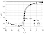
이하, 전술한 실시예들에 따른 포토 트랜지스터의 빛 흡수 특성에 대해 살펴보기로 한다. 하기에서는 도 2에 도시된 실시예에 따른 포토 트랜지스터를 실시예로 개시하고, 도 2에서 제2 활성층이 생략된 구조의 포토 트랜지스터를 비교예로 개시하기로 한다.Hereinafter, the light absorption characteristics of the phototransistor according to the above-described embodiments will be examined. Below, the phototransistor according to the embodiment illustrated in Fig. 2 will be disclosed as an example, and the phototransistor having a structure in which the second active layer is omitted in Fig. 2 will be disclosed as a comparative example.
실시예Example
전술한 도 2에 도시된 실시예에 따른 포토 트랜지스터를 제조하였다. 이때, 제1 활성층은 150nm의 두께로 IGZO 단일층을 형성하였고, 제2 활성층은 150nm의 두께로 셀레늄 단일층을 형성하였다.A phototransistor was manufactured according to the embodiment illustrated in Fig. 2 described above. At this time, the first active layer was formed as an IGZO single layer with a thickness of 150 nm, and the second active layer was formed as a selenium single layer with a thickness of 150 nm.
비교예Comparative example
제2 활성층을 구비하지 않고 전술한 실시예와 동일한 조건으로 포토 트랜지스터를 제조하였다.A phototransistor was manufactured under the same conditions as the above-described example without the second active layer.
전술한 실시예 및 비교예에 따라 제조된 포토 트랜지스터에 적색 및 녹색 빛을 다양한 강도(intensity)로 각각 조사한 상태에서 게이트 전압에 따른 드레인 전류를 측정하였다.The phototransistors manufactured according to the above-described examples and comparative examples were irradiated with red and green light at various intensities, and the drain current according to the gate voltage was measured.
도 13은 실시예에 따른 포토 트랜지스터에 녹색 빛을 조사하고 게이트 전압에 따른 드레인 전류를 측정한 그래프이고, 도 14는 비교예에 따른 포토 트랜지스터에 녹색 빛을 조사하고 게이트 전압에 따른 드레인 전류를 측정한 그래프이다. 여기서, 녹색 빛은 532nm의 파장과 2.33eV의 에너지를 가진 빛을 사용하였다.Fig. 13 is a graph showing the results of measuring the drain current according to the gate voltage by irradiating green light on a phototransistor according to an embodiment, and Fig. 14 is a graph showing the results of measuring the drain current according to the gate voltage by irradiating green light on a phototransistor according to a comparative example. Here, the green light used was light with a wavelength of 532 nm and an energy of 2.33 eV.
도 13을 참조하면, 실시예에 따른 포토 트랜지스터에 적색 빛을 조사하지 않았을 때에는 게이트 전압에 따른 드레인 전류의 변화가 거의 나타나지 않았다. 실시예에 따른 포토 트랜지스터에 1, 5, 10mW/㎟의 강도로 각각 녹색 빛을 조사한 경우, 게이트 전압에 따른 드레인 전류가 점점 커지는 것으로 나타났다. -10V의 게이트 전압에서 녹색 빛을 조사하지 않은 경우와 10mW/㎟의 강도로 녹색 빛을 조사한 경우의 드레인 전류 차이는 대략 109배의 차이가 나타났다. 또한, 녹색 빛을 조사하지 않은 경우와 녹색 빛을 조사한 경우의 게이트 온 전압 변화량은 대략 26V로 나타났다. 또한, 실시예의 포토 트랜지스터는 녹색 빛을 조사하면 문턱 전압이 음의 방향으로 이동하고 오프 전류(Off Current)가 크게 증가하였다.Referring to Fig. 13, when the phototransistor according to the embodiment was not irradiated with red light, there was almost no change in the drain current according to the gate voltage. When the phototransistor according to the embodiment was irradiated with green light at intensities of 1, 5, and 10 mW/mm2, the drain current was found to gradually increase according to the gate voltage. The difference in drain current between the case where green light was not irradiated at a gate voltage of -10 V and the case where green light was irradiated at an intensity of 10 mW/mm2 was approximately 109 times. In addition, the gate on voltage change amount between the case where green light was not irradiated and the case where green light was irradiated was approximately 26 V. In addition, when the phototransistor of the embodiment was irradiated with green light, the threshold voltage shifted in the negative direction and the off current increased significantly.
반면, 도 14를 참조하면, 비교예에 따른 포토 트랜지스터에 빛을 조사하지 않았을 때에는 게이트 전압에 따른 드레인 전류의 변화가 거의 나타나지 않았다. 비교예에 따른 포토 트랜지스터에 1, 5, 10mW/㎟의 강도로 각각 녹색 빛을 조사한 경우, 게이트 전압에 따른 드레인 전류가 미세하게 커지는 것으로 나타났다. 또한, 녹색 빛을 조사하지 않은 경우와 녹색 빛을 조사한 경우의 게이트 온 전압 변화량은 대략 4V로 나타났다. 또한, 비교예의 포토 트랜지스터는 녹색 빛을 조사하면 문턱 전압이 미세하게 음의 방향으로 이동하고 오프 전류는 변화가 없었다.On the other hand, referring to Fig. 14, when the phototransistor according to the comparative example was not irradiated with light, there was almost no change in the drain current according to the gate voltage. When the phototransistor according to the comparative example was irradiated with green light at intensities of 1, 5, and 10 mW/mm2, the drain current according to the gate voltage was found to increase slightly. In addition, the change in gate on voltage between the case where green light was not irradiated and the case where green light was irradiated was found to be approximately 4 V. In addition, when the phototransistor of the comparative example was irradiated with green light, the threshold voltage shifted slightly in the negative direction and the off current did not change.
하기 표 1은 녹색 빛에 대한 실시예 및 비교예에 따른 포토 트랜지스터의 특성인 광 응답률(photoresponsibity), 광민감도(photosensitivity) 및 검출률(detectivity)을 측정하여 나타내었다.Table 1 below shows the photoresponsibity, photosensitivity, and detectivity, which are the characteristics of phototransistors according to examples and comparative examples for green light.
상기 표 1을 참조하면, 실시예에 따른 포토 트랜지스터는 비교예에 비해 광 응답률, 광민감도 및 검출률 값이 현저하게 큰 것을 알 수 있다.이를 통해, 제1 활성층 및 제2 활성층을 구비한 실시예의 포토 트랜지스터는 녹색 빛을 흡수하여 트랜지스터로 동작함을 알 수 있으나, 비교예의 포토 트랜지스터는 녹색 빛을 거의 흡수하지 못하여 트랜지스터로 동작하지 못함을 알 수 있었다.Referring to Table 1 above, it can be seen that the phototransistor according to the embodiment has significantly greater light response rate, light sensitivity, and detection rate values than the comparative example. Through this, it can be seen that the phototransistor of the embodiment having the first active layer and the second active layer absorbs green light and operates as a transistor, but the phototransistor of the comparative example hardly absorbs green light and thus cannot operate as a transistor.
도 15는 실시예에 따른 포토 트랜지스터에 적색 빛을 조사하고 게이트 전압에 따른 드레인 전류를 측정한 그래프이고, 도 16은 비교예에 따른 포토 트랜지스터에 적색 빛을 조사하고 게이트 전압에 따른 드레인 전류를 측정한 그래프이다. 여기서, 적색 빛은 635nm의 파장과 1.95eV의 에너지를 가진 빛을 사용하였다.Fig. 15 is a graph showing the results of measuring the drain current according to the gate voltage by irradiating red light on a phototransistor according to an embodiment, and Fig. 16 is a graph showing the results of measuring the drain current according to the gate voltage by irradiating red light on a phototransistor according to a comparative example. Here, the red light used was light with a wavelength of 635 nm and an energy of 1.95 eV.
도 15를 참조하면, 실시예에 따른 포토 트랜지스터에 적색 빛을 조사하지 않았을 때에는 게이트 전압에 따른 드레인 전류의 변화가 거의 나타나지 않았다. 실시예에 따른 포토 트랜지스터에 1, 5, 10mW/㎟의 강도로 각각 적색 빛을 조사한 경우, 게이트 전압에 따른 드레인 전류가 점점 커지는 것으로 나타났다. -10V의 게이트 전압에서 적색 빛을 조사하지 않은 경우와 10mW/㎟의 강도로 적색 빛을 조사한 경우의 드레인 전류 차이는 대략 108배의 차이가 나타났다. 또한, 적색 빛을 조사하지 않은 경우와 적색 빛을 조사한 경우의 게이트 온 전압 변화량은 대략 16.6V로 나타났다. 또한, 실시예의 포토 트랜지스터는 적색 빛을 조사하면 문턱 전압이 음의 방향으로 이동하였다.Referring to Fig. 15, when the phototransistor according to the embodiment was not irradiated with red light, there was almost no change in the drain current according to the gate voltage. When the phototransistor according to the embodiment was irradiated with red light at intensities of 1, 5, and 10 mW/mm2, the drain current was found to gradually increase according to the gate voltage. The difference in drain current between the case where red light was not irradiated at a gate voltage of -10 V and the case where red light was irradiated at an intensity of 10 mW/mm2 was approximately 108 times. In addition, the gate-on voltage change amount between the case where red light was not irradiated and the case where red light was irradiated was approximately 16.6 V. In addition, the threshold voltage of the phototransistor of the embodiment shifted in the negative direction when irradiated with red light.
반면, 도 16을 참조하면, 비교예에 따른 포토 트랜지스터에 적색 빛을 조사하지 않았을 때에는 게이트 전압에 따른 드레인 전류의 변화가 거의 나타나지 않았다. 비교예에 따른 포토 트랜지스터에 1, 5, 10mW/㎟의 강도로 각각 적색 빛을 조사한 경우, 게이트 전압에 따른 드레인 전류가 미세하게 커지는 것으로 나타났다. 또한, 적색 빛을 조사하지 않은 경우와 적색 빛을 조사한 경우의 게이트 온 전압 변화량은 나타나지 않았다. 또한, 비교예의 포토 트랜지스터는 적색 빛을 조사하여도 문턱 전압이나 오프 전류에 변화가 없었다.On the other hand, referring to Fig. 16, when the phototransistor according to the comparative example was not irradiated with red light, there was almost no change in the drain current according to the gate voltage. When the phototransistor according to the comparative example was irradiated with red light at intensities of 1, 5, and 10 mW/mm2, the drain current according to the gate voltage was found to slightly increase. In addition, there was no change in the gate on voltage between the cases where the red light was not irradiated and when the red light was irradiated. In addition, the phototransistor of the comparative example showed no change in the threshold voltage or off current even when irradiated with red light.
하기 표 2는 적색 빛에 대한 실시예 및 비교예에 따른 포토 트랜지스터의 특성인 광 응답률, 광민감도 및 검출률을 측정하여 나타내었다.Table 2 below shows the characteristics of phototransistors according to examples and comparative examples for red light, such as light response rate, light sensitivity, and detection rate.
상기 표 1을 참조하면, 실시예에 따른 포토 트랜지스터는 비교예에 비해 광 응답률, 광민감도 및 검출율 값이 현저하게 큰 것을 알 수 있다.이를 통해, 제1 활성층 및 제2 활성층을 구비한 실시예의 포토 트랜지스터는 적색 빛을 흡수하여 트랜지스터로 동작함을 알 수 있으나, 비교예의 포토 트랜지스터는 적색 빛을 흡수하지 못하여 트랜지스터로 동작하지 못함을 알 수 있었다.Referring to Table 1 above, it can be seen that the phototransistor according to the embodiment has significantly greater light response rate, light sensitivity, and detection rate values than the comparative example. Through this, it can be seen that the phototransistor of the embodiment having the first active layer and the second active layer absorbs red light and operates as a transistor, but the phototransistor of the comparative example does not absorb red light and therefore does not operate as a transistor.
도 17은 비교예에 따른 포토 트랜지스터에 청색 빛을 조사하고 게이트 전압에 따른 드레인 전류를 측정한 그래프이다. 여기서, 청색 빛은 405nm의 파장과 3.06eV의 에너지를 가진 빛을 사용하였다.Figure 17 is a graph showing the results of measuring the drain current according to the gate voltage by irradiating blue light on a phototransistor according to a comparative example. Here, the blue light used was light with a wavelength of 405 nm and energy of 3.06 eV.
도 17을 참조하면, 비교예에 따른 포토 트랜지스터에 청색 빛을 조사하지 않았을 때에는 게이트 전압에 따른 드레인 전류의 변화가 거의 나타나지 않았다. 비교예에 따른 포토 트랜지스터에 1, 3, 5, 10mW/㎟의 강도로 각각 청색 빛을 조사한 경우, 게이트 전압에 따른 드레인 전류가 점점 커지는 것으로 나타났다. 청색 빛을 조사하지 않은 경우와 청색 빛을 조사한 경우의 게이트 온 전압 변화량은 대략 30V로 나타났다. 또한, 실시예의 포토 트랜지스터는 적색 빛을 조사하면 문턱 전압이 음의 방향으로 이동하였다.Referring to Fig. 17, when the phototransistor according to the comparative example was not irradiated with blue light, there was almost no change in the drain current according to the gate voltage. When the phototransistor according to the comparative example was irradiated with blue light at intensities of 1, 3, 5, and 10 mW/mm2, the drain current according to the gate voltage gradually increased. The amount of change in the gate-on voltage when the blue light was not irradiated and when the blue light was irradiated was approximately 30 V. In addition, the threshold voltage of the phototransistor of the embodiment shifted in the negative direction when red light was irradiated.
이를 통해, IGZO의 제1 활성층만을 구비한 비교예에 따른 포토 트랜지스터는 청색 빛을 흡수하여 포토 트랜지스터로 작동함을 알 수 있었다.Through this, it was found that the phototransistor according to the comparative example having only the first active layer of IGZO operates as a phototransistor by absorbing blue light.
전술한 도 13 내지 도 17에 나타난 실시예 및 비교예에 따른 포토 트랜지스터의 빛 흡수 특성을 살펴본 바와 같이, IGZO의 제1 활성층만을 구비한 비교예에 따른 포토 트랜지스터는 청색 빛을 흡수할 뿐 녹색과 적색 빛은 흡수하지 못하였다. 반면, IGZO의 제1 활성층에 셀레늄의 제2 활성층을 더 구비한 실시예에 따른 포토 트랜지스터는 녹색과 적색 빛을 흡수하였다. 따라서, 실시예에 따른 포토 트랜지스터는 IGZO의 제1 활성층을 보완하여 셀레늄의 제2 활성층에서 녹색 및 적색 빛을 흡수함으로써, 가시광 파장대의 빛을 모두 흡수하여 광 센서로의 특성을 향상시킬 수 있다.As examined in the light absorption characteristics of the phototransistors according to the embodiments and comparative examples shown in the above-described FIGS. 13 to 17, the phototransistor according to the comparative example having only the first active layer of IGZO absorbed blue light but did not absorb green and red light. On the other hand, the phototransistor according to the embodiment having the second active layer of selenium in the first active layer of IGZO absorbed green and red light. Therefore, the phototransistor according to the embodiment can improve the characteristics as a light sensor by absorbing all light in the visible wavelength range by supplementing the first active layer of IGZO and absorbing green and red light in the second active layer of selenium.
도 17은 전술한 실시예에 따른 포토 트랜지스터 구동 시 시간에 따른 드레인 전류를 측정한 그래프이다. 여기서, 포토 트랜지스터 구동은 일정 가시광을 조사한 상태에서 10초 주기로 게이트를 온/오프하였다.Fig. 17 is a graph showing the drain current measured over time when driving a phototransistor according to the above-described embodiment. Here, the phototransistor was driven by turning the gate on and off in a 10-second cycle while irradiating it with a constant visible light.
도 17을 참조하면, 실시예에 따른 포토 트랜지스터는 게이트 온의 경우 드레인 전류 값이 일정하게 유지되는 것으로 나타났다. 또한, 게이트 오프와 온 사이 동안 발생하는 드레인 전류인 잔류성 광전류(persistent photocurrent: PPC)가 나타났다. 전술한 비교예의 IGZO 단일 활성층을 구비한 포토 트랜지스터는 잔류성 광전류가 양(그래프 상 빗금친 면적)이 매우 크다고 알려져 있으나, 실시예의 포토 트랜지스터는 잔류성 광전류의 양이 작게 나타났다.Referring to FIG. 17, the phototransistor according to the embodiment exhibited a constant drain current value when the gate was turned on. In addition, a persistent photocurrent (PPC), which is a drain current that occurs between the gate-off and -on states, was exhibited. The phototransistor having the IGZO single active layer of the comparative example described above is known to have a very large amount of residual photocurrent (the hatched area on the graph), but the phototransistor of the embodiment exhibited a small amount of residual photocurrent.
이를 통해, 실시예에 따른 포토 트랜지스터는 드레인 전류 값이 일정하게 유지되고, 잔류성 광전류의 양이 작아 포토 트랜지스터로의 특성이 우수함을 알 수 있다.Through this, it can be seen that the phototransistor according to the embodiment has excellent characteristics as a phototransistor because the drain current value is maintained constant and the amount of residual photocurrent is small.
상기와 같이, 일 실시예에 따른 포토 트랜지스터에 의하면, 금속 산화물을 포함하는 제1 활성층에 더해 셀레늄을 포함하는 제2 활성층을 포함함으로써, 가시광 파장대 전체의 빛을 흡수함으로써, 광 센싱 특성을 향상시킬 수 있다. 또한, 포토 트랜지스터의 광 응답률, 광민감도 및 검출율을 향상시킬 수 있다. 또한, 일 실시예에 따른 표시 장치에 의하면, 특성이 우수한 포토 트랜지스터를 구비함으로써, 표시 장치의 광 센싱 특성을 향상시킬 수 있다.As described above, according to the phototransistor according to one embodiment, by including a second active layer including selenium in addition to a first active layer including a metal oxide, light sensing characteristics can be improved by absorbing light in the entire visible light wavelength range. In addition, the optical response rate, optical sensitivity, and detectivity of the phototransistor can be improved. In addition, according to the display device according to one embodiment, by having a phototransistor with excellent characteristics, the optical sensing characteristics of the display device can be improved.
이상 첨부된 도면을 참조하여 본 발명의 실시예들을 설명하였지만, 본 발명이 속하는 기술분야에서 통상의 지식을 가진 자는 본 발명의 그 기술적 사상이나 필수적인 특징을 변경하지 않고서 다른 구체적인 형태로 실시될 수 있다는 것을 이해할 수 있을 것이다. 그러므로 이상에서 기술한 실시예들은 모든 면에서 예시적인 것이며 한정적이 아닌 것으로 이해해야만 한다.Although the embodiments of the present invention have been described with reference to the attached drawings, those skilled in the art will understand that the present invention can be implemented in other specific forms without changing the technical idea or essential features of the present invention. Therefore, it should be understood that the embodiments described above are exemplary in all respects and not restrictive.
1: 포토 트랜지스터110: 기판
120: 게이트 전극130: 게이트 절연막
140: 제1 활성층150: 제2 활성층
160: 소스 전극170: 드레인 전극1: Phototransistor 110: Substrate
120: Gate electrode 130: Gate insulating film
140: 1st active layer 150: 2nd active layer
160: Source electrode 170: Drain electrode
Claims (20)
Translated fromKorean상기 게이트 전극을 절연시키는 게이트 절연막;
상기 게이트 절연막을 사이에 두고 상기 게이트 전극과 중첩하며, 금속 산화물을 포함하는 제1 활성층;
상기 제1 활성층 상에 배치되며, 셀레늄을 포함하는 제2 활성층; 및
상기 제2 활성층에 각각 연결되는 소스 전극 및 드레인 전극을 포함하며,
상기 제1 활성층은 IGZO로 형성되고, 상기 제2 활성층은 오직 셀레늄으로 형성된 포토 트랜지스터.A gate electrode arranged on a substrate;
A gate insulating film that insulates the above gate electrode;
A first active layer overlapping the gate electrode with the gate insulating film interposed therebetween and including a metal oxide;
A second active layer disposed on the first active layer and containing selenium; and
It includes a source electrode and a drain electrode each connected to the second active layer,
A phototransistor in which the first active layer is formed of IGZO and the second active layer is formed only of selenium.
상기 제1 활성층과 상기 제2 활성층은 상기 게이트 전극과 중첩하는 영역에서 서로 접하는 포토 트랜지스터.In the first paragraph,
A phototransistor in which the first active layer and the second active layer are in contact with each other in a region overlapping the gate electrode.
상기 제1 활성층은 상기 제2 활성층보다 상기 게이트 전극에 인접하여 배치되는 포토 트랜지스터.In the second paragraph,
A phototransistor in which the first active layer is positioned closer to the gate electrode than the second active layer.
상기 소스 전극은 상기 제2 활성층의 일부를 덮고, 상기 드레인 전극은 상기 제2 활성층의 다른 일부를 덮는 포토 트랜지스터.In the first paragraph,
A phototransistor wherein the source electrode covers a portion of the second active layer, and the drain electrode covers another portion of the second active layer.
상기 제1 활성층의 측벽과 상기 제2 활성층의 측벽은 서로 접하여 상호 정렬되는 포토 트랜지스터.In the fourth paragraph,
A phototransistor in which the sidewalls of the first active layer and the sidewalls of the second active layer are in contact with each other and are aligned with each other.
상기 소스 전극 및 상기 드레인 전극 각각은 상기 제1 활성층과 상기 제2 활성층 사이에 배치되는 포토 트랜지스터.In the first paragraph,
A phototransistor wherein each of the source electrode and the drain electrode is positioned between the first active layer and the second active layer.
상기 제2 활성층의 두께는 5 내지 300nm인 포토 트랜지스터.In the first paragraph,
A phototransistor wherein the thickness of the second active layer is 5 to 300 nm.
상기 기판 상에 배치되며, 제1 트랜지스터 및 제2 트랜지스터를 포함하는 트랜지스터층;
상기 트랜지스터층 상에 배치되며, 적어도 제1 전극을 포함하는 발광 소자층; 및
상기 발광 소자층 상에 배치되며, 복수의 전극들을 포함하는 터치 센싱 유닛을 포함하며,
상기 제1 트랜지스터는 게이트 전극, 금속 산화물을 포함하는 제1 활성층, 셀레늄을 포함하는 제2 활성층, 및 소스 전극과 드레인 전극을 포함하며,
상기 제1 활성층은 IGZO로 형성되고, 상기 제2 활성층은 오직 셀레늄으로 형성된 표시 장치.A substrate comprising a transmissive region and an emitting region;
A transistor layer disposed on the substrate and including a first transistor and a second transistor;
A light emitting element layer disposed on the transistor layer and including at least a first electrode; and
A touch sensing unit is disposed on the light emitting element layer and includes a plurality of electrodes,
The first transistor includes a gate electrode, a first active layer including a metal oxide, a second active layer including selenium, and a source electrode and a drain electrode.
A display device wherein the first active layer is formed of IGZO and the second active layer is formed only of selenium.
상기 제1 트랜지스터는 상기 기판의 상기 투과 영역과 중첩하고, 상기 제2 트랜지스터는 상기 발광 영역과 중첩하는 표시 장치.In Article 11,
A display device wherein the first transistor overlaps the transmitting region of the substrate, and the second transistor overlaps the emitting region.
상기 제1 트랜지스터는 상기 발광 소자층의 상기 제1 전극과 비중첩하고, 상기 터치 센싱 유닛의 상기 복수의 전극들과 비중첩하는 표시 장치.In Article 12,
A display device wherein the first transistor does not overlap with the first electrode of the light-emitting element layer and does not overlap with the plurality of electrodes of the touch sensing unit.
상기 제2 트랜지스터는 상기 발광 소자층의 상기 제1 전극과 중첩하고, 상기 터치 센싱 유닛의 상기 복수의 전극들과 비중첩하는 표시 장치.In Article 13,
A display device in which the second transistor overlaps the first electrode of the light-emitting element layer and does not overlap the plurality of electrodes of the touch sensing unit.
상기 발광 소자층은 상기 제1 전극, 상기 제1 전극과 대향하는 제2 전극, 및 상기 제1 전극과 상기 제2 전극 사이에 개재된 유기 발광층을 더 포함하며,
상기 제1 트랜지스터 및 상기 제2 트랜지스터는 상기 제2 전극과 중첩하는 표시 장치.In Article 11,
The light-emitting element layer further includes the first electrode, a second electrode facing the first electrode, and an organic light-emitting layer interposed between the first electrode and the second electrode,
A display device in which the first transistor and the second transistor overlap with the second electrode.
상기 발광 소자층과 상기 터치 센싱 유닛 사이에 배치된 박막 봉지층을 더 포함하는 표시 장치.In Article 11,
A display device further comprising a thin film encapsulation layer disposed between the light emitting element layer and the touch sensing unit.
상기 터치 센싱 유닛의 상기 복수의 전극들은 구동 전극들과 감지 전극들을 포함하는 표시 장치.In Article 11,
A display device wherein the plurality of electrodes of the touch sensing unit include driving electrodes and sensing electrodes.
상기 제1 활성층과 상기 제2 활성층은 상기 게이트 전극과 중첩하는 영역에서 서로 접하는 표시 장치.In Article 11,
A display device in which the first active layer and the second active layer are in contact with each other in a region overlapping the gate electrode.
상기 제1 활성층은 상기 제2 활성층보다 상기 게이트 전극에 인접하여 배치되는 표시 장치.In Article 18,
A display device in which the first active layer is positioned closer to the gate electrode than the second active layer.
Priority Applications (3)
| Application Number | Priority Date | Filing Date | Title |
|---|---|---|---|
| KR1020190174429AKR102756389B1 (en) | 2019-12-24 | 2019-12-24 | Photo transistor and display device comprising of the same |
| CN202011259707.6ACN113035981B (en) | 2019-12-24 | 2020-11-12 | Phototransistor and display device including the same |
| US17/115,942US11690273B2 (en) | 2019-12-24 | 2020-12-09 | Photo transistor and display device including the same |
Applications Claiming Priority (1)
| Application Number | Priority Date | Filing Date | Title |
|---|---|---|---|
| KR1020190174429AKR102756389B1 (en) | 2019-12-24 | 2019-12-24 | Photo transistor and display device comprising of the same |
Publications (2)
| Publication Number | Publication Date |
|---|---|
| KR20210082319A KR20210082319A (en) | 2021-07-05 |
| KR102756389B1true KR102756389B1 (en) | 2025-01-17 |
Family
ID=76438430
Family Applications (1)
| Application Number | Title | Priority Date | Filing Date |
|---|---|---|---|
| KR1020190174429AActiveKR102756389B1 (en) | 2019-12-24 | 2019-12-24 | Photo transistor and display device comprising of the same |
Country Status (3)
| Country | Link |
|---|---|
| US (1) | US11690273B2 (en) |
| KR (1) | KR102756389B1 (en) |
| CN (1) | CN113035981B (en) |
Families Citing this family (2)
| Publication number | Priority date | Publication date | Assignee | Title |
|---|---|---|---|---|
| CN113192975B (en)* | 2021-04-08 | 2023-12-01 | 深圳市华星光电半导体显示技术有限公司 | Display device and preparation method thereof |
| CN115881781A (en)* | 2021-08-18 | 2023-03-31 | 南京京东方显示技术有限公司 | Thin film transistor device and manufacturing method, display substrate |
Citations (3)
| Publication number | Priority date | Publication date | Assignee | Title |
|---|---|---|---|---|
| JP2019009367A (en)* | 2017-06-28 | 2019-01-17 | セイコーエプソン株式会社 | Photoelectric conversion device manufacturing method, photoelectric conversion device, and electronic apparatus |
| WO2019021462A1 (en)* | 2017-07-28 | 2019-01-31 | シャープ株式会社 | DISPLAY DEVICE |
| CN110034168A (en)* | 2019-03-29 | 2019-07-19 | 上海天马微电子有限公司 | Display panel and display device |
Family Cites Families (12)
| Publication number | Priority date | Publication date | Assignee | Title |
|---|---|---|---|---|
| TWI501319B (en)* | 2008-12-26 | 2015-09-21 | Semiconductor Energy Lab | Semiconductor device and manufacturing method thereof |
| TWI414765B (en) | 2010-12-03 | 2013-11-11 | E Ink Holdings Inc | Light sensing circuit unit |
| KR101680768B1 (en)* | 2010-12-10 | 2016-11-29 | 삼성전자주식회사 | Transistor and electronic device including the same |
| KR101810608B1 (en)* | 2011-06-22 | 2017-12-21 | 삼성전자주식회사 | Light sensing apparatus and method of driving the light sensing apparatus, and optical touch screen apparatus including the light sensing apparatus |
| KR101851567B1 (en) | 2011-07-04 | 2018-04-25 | 삼성전자주식회사 | Transistor, electronic device including transistor and manufacturing methods thereof |
| KR101899482B1 (en)* | 2011-11-25 | 2018-09-18 | 삼성전자주식회사 | Light sensing circuit, method of fabricating the light sensing circuit, and optical touch panel including the light sensing circuit |
| US10027896B2 (en) | 2016-01-15 | 2018-07-17 | Semiconductor Energy Laboratory Co., Ltd. | Image display system, operation method of the same, and electronic device |
| KR102679068B1 (en)* | 2016-08-23 | 2024-07-02 | 삼성디스플레이 주식회사 | Display device |
| KR102403812B1 (en)* | 2017-06-01 | 2022-05-30 | 엘지디스플레이 주식회사 | Sensing unit including touch electrode and display using the same |
| KR102428557B1 (en) | 2017-11-20 | 2022-08-02 | 엘지디스플레이 주식회사 | Oxide semiconductor phototransistor improved in visible light absorption rate and manufacturing method thereof |
| KR102509439B1 (en)* | 2018-03-06 | 2023-03-13 | 삼성디스플레이 주식회사 | Fingerprint sensor package and display device including the same |
| CN110176203B (en)* | 2018-05-09 | 2021-03-16 | 京东方科技集团股份有限公司 | Array substrate and display device |
- 2019
- 2019-12-24KRKR1020190174429Apatent/KR102756389B1/enactiveActive
- 2020
- 2020-11-12CNCN202011259707.6Apatent/CN113035981B/enactiveActive
- 2020-12-09USUS17/115,942patent/US11690273B2/enactiveActive
Patent Citations (3)
| Publication number | Priority date | Publication date | Assignee | Title |
|---|---|---|---|---|
| JP2019009367A (en)* | 2017-06-28 | 2019-01-17 | セイコーエプソン株式会社 | Photoelectric conversion device manufacturing method, photoelectric conversion device, and electronic apparatus |
| WO2019021462A1 (en)* | 2017-07-28 | 2019-01-31 | シャープ株式会社 | DISPLAY DEVICE |
| CN110034168A (en)* | 2019-03-29 | 2019-07-19 | 上海天马微电子有限公司 | Display panel and display device |
Also Published As
| Publication number | Publication date |
|---|---|
| CN113035981A (en) | 2021-06-25 |
| KR20210082319A (en) | 2021-07-05 |
| US11690273B2 (en) | 2023-06-27 |
| CN113035981B (en) | 2024-08-23 |
| US20210193753A1 (en) | 2021-06-24 |
Similar Documents
| Publication | Publication Date | Title |
|---|---|---|
| US11956990B2 (en) | Display device with metal tip protruding toward groove center | |
| CN110286796B (en) | Electronic substrate, manufacturing method thereof and display panel | |
| KR102372091B1 (en) | Organic light emitting display device and method of manufacturing the same | |
| CN111564506B (en) | Photosensitive sensor, preparation method thereof and electronic equipment | |
| TWI814369B (en) | Photosensitive device substrate and manufacturing method thereof | |
| EP3242341A1 (en) | Array substrate and manufacturing method therefor, display panel and display device | |
| CN103151369B (en) | A kind of dot structure and preparation method thereof | |
| US20110127499A1 (en) | Organic light emitting diode display device and method of fabricating the same | |
| CN104681623A (en) | Oxide thin film transistor and array substrate including the same | |
| KR102276146B1 (en) | Thin film transistor substrate and method of manufacturing the same | |
| US20240114743A1 (en) | Display module having increased transmittance and electronic device including the display module | |
| EP4095926A2 (en) | Display apparatus | |
| TW201123442A (en) | Organic light emitting display and manufacturing method thereof | |
| US20230217802A1 (en) | Display panel and electric apparatus including the same | |
| KR102756389B1 (en) | Photo transistor and display device comprising of the same | |
| CN113571657A (en) | Display panel and display device including the same | |
| US20220310972A1 (en) | Display panel and method of manufacturing the same | |
| CN114649369A (en) | Display device and method of manufacturing the same | |
| CN112670300A (en) | Display module, preparation method and display device | |
| KR102132412B1 (en) | Thin fim transistor array substrate for display device and method fabricating the same | |
| WO2020192452A1 (en) | Conductive structure, touch structure, and touch display device | |
| US20240065045A1 (en) | Display panel and method of manufacturing the same | |
| CN113066798B (en) | Driving substrate, display panel and manufacturing method of driving substrate | |
| CN116799008A (en) | Display device and method of manufacturing the same | |
| KR20240024382A (en) | Phototransistor, display device and method of the phototransistor |
Legal Events
| Date | Code | Title | Description |
|---|---|---|---|
| PA0109 | Patent application | Patent event code:PA01091R01D Comment text:Patent Application Patent event date:20191224 | |
| PG1501 | Laying open of application | ||
| PA0201 | Request for examination | Patent event code:PA02012R01D Patent event date:20221007 Comment text:Request for Examination of Application Patent event code:PA02011R01I Patent event date:20191224 Comment text:Patent Application | |
| E902 | Notification of reason for refusal | ||
| PE0902 | Notice of grounds for rejection | Comment text:Notification of reason for refusal Patent event date:20240220 Patent event code:PE09021S01D | |
| E701 | Decision to grant or registration of patent right | ||
| PE0701 | Decision of registration | Patent event code:PE07011S01D Comment text:Decision to Grant Registration Patent event date:20241025 | |
| GRNT | Written decision to grant | ||
| PR0701 | Registration of establishment | Comment text:Registration of Establishment Patent event date:20250114 Patent event code:PR07011E01D | |
| PR1002 | Payment of registration fee | Payment date:20250114 End annual number:3 Start annual number:1 | |
| PG1601 | Publication of registration |