KR102755468B1 - Display device - Google Patents
Display deviceDownload PDFInfo
- Publication number
- KR102755468B1 KR102755468B1KR1020200004984AKR20200004984AKR102755468B1KR 102755468 B1KR102755468 B1KR 102755468B1KR 1020200004984 AKR1020200004984 AKR 1020200004984AKR 20200004984 AKR20200004984 AKR 20200004984AKR 102755468 B1KR102755468 B1KR 102755468B1
- Authority
- KR
- South Korea
- Prior art keywords
- pixel
- area
- electrode
- display device
- common electrode
- Prior art date
- Legal status (The legal status is an assumption and is not a legal conclusion. Google has not performed a legal analysis and makes no representation as to the accuracy of the status listed.)
- Active
Links
Images


Classifications
- G—PHYSICS
- G09—EDUCATION; CRYPTOGRAPHY; DISPLAY; ADVERTISING; SEALS
- G09F—DISPLAYING; ADVERTISING; SIGNS; LABELS OR NAME-PLATES; SEALS
- G09F9/00—Indicating arrangements for variable information in which the information is built-up on a support by selection or combination of individual elements
- G09F9/30—Indicating arrangements for variable information in which the information is built-up on a support by selection or combination of individual elements in which the desired character or characters are formed by combining individual elements
- G09F9/33—Indicating arrangements for variable information in which the information is built-up on a support by selection or combination of individual elements in which the desired character or characters are formed by combining individual elements being semiconductor devices, e.g. diodes
- G—PHYSICS
- G06—COMPUTING OR CALCULATING; COUNTING
- G06F—ELECTRIC DIGITAL DATA PROCESSING
- G06F3/00—Input arrangements for transferring data to be processed into a form capable of being handled by the computer; Output arrangements for transferring data from processing unit to output unit, e.g. interface arrangements
- G06F3/01—Input arrangements or combined input and output arrangements for interaction between user and computer
- G06F3/03—Arrangements for converting the position or the displacement of a member into a coded form
- G06F3/041—Digitisers, e.g. for touch screens or touch pads, characterised by the transducing means
- G06F3/0416—Control or interface arrangements specially adapted for digitisers
- G06F3/04164—Connections between sensors and controllers, e.g. routing lines between electrodes and connection pads
- G—PHYSICS
- G06—COMPUTING OR CALCULATING; COUNTING
- G06F—ELECTRIC DIGITAL DATA PROCESSING
- G06F3/00—Input arrangements for transferring data to be processed into a form capable of being handled by the computer; Output arrangements for transferring data from processing unit to output unit, e.g. interface arrangements
- G06F3/01—Input arrangements or combined input and output arrangements for interaction between user and computer
- G06F3/03—Arrangements for converting the position or the displacement of a member into a coded form
- G06F3/041—Digitisers, e.g. for touch screens or touch pads, characterised by the transducing means
- G06F3/0412—Digitisers structurally integrated in a display
- G—PHYSICS
- G06—COMPUTING OR CALCULATING; COUNTING
- G06F—ELECTRIC DIGITAL DATA PROCESSING
- G06F3/00—Input arrangements for transferring data to be processed into a form capable of being handled by the computer; Output arrangements for transferring data from processing unit to output unit, e.g. interface arrangements
- G06F3/01—Input arrangements or combined input and output arrangements for interaction between user and computer
- G06F3/03—Arrangements for converting the position or the displacement of a member into a coded form
- G06F3/041—Digitisers, e.g. for touch screens or touch pads, characterised by the transducing means
- G06F3/044—Digitisers, e.g. for touch screens or touch pads, characterised by the transducing means by capacitive means
- G06F3/0445—Digitisers, e.g. for touch screens or touch pads, characterised by the transducing means by capacitive means using two or more layers of sensing electrodes, e.g. using two layers of electrodes separated by a dielectric layer
- G—PHYSICS
- G06—COMPUTING OR CALCULATING; COUNTING
- G06F—ELECTRIC DIGITAL DATA PROCESSING
- G06F3/00—Input arrangements for transferring data to be processed into a form capable of being handled by the computer; Output arrangements for transferring data from processing unit to output unit, e.g. interface arrangements
- G06F3/01—Input arrangements or combined input and output arrangements for interaction between user and computer
- G06F3/03—Arrangements for converting the position or the displacement of a member into a coded form
- G06F3/041—Digitisers, e.g. for touch screens or touch pads, characterised by the transducing means
- G06F3/044—Digitisers, e.g. for touch screens or touch pads, characterised by the transducing means by capacitive means
- G06F3/0446—Digitisers, e.g. for touch screens or touch pads, characterised by the transducing means by capacitive means using a grid-like structure of electrodes in at least two directions, e.g. using row and column electrodes
- H—ELECTRICITY
- H10—SEMICONDUCTOR DEVICES; ELECTRIC SOLID-STATE DEVICES NOT OTHERWISE PROVIDED FOR
- H10K—ORGANIC ELECTRIC SOLID-STATE DEVICES
- H10K50/00—Organic light-emitting devices
- H10K50/80—Constructional details
- H—ELECTRICITY
- H10—SEMICONDUCTOR DEVICES; ELECTRIC SOLID-STATE DEVICES NOT OTHERWISE PROVIDED FOR
- H10K—ORGANIC ELECTRIC SOLID-STATE DEVICES
- H10K59/00—Integrated devices, or assemblies of multiple devices, comprising at least one organic light-emitting element covered by group H10K50/00
- H10K59/10—OLED displays
- H10K59/12—Active-matrix OLED [AMOLED] displays
- H10K59/121—Active-matrix OLED [AMOLED] displays characterised by the geometry or disposition of pixel elements
- H—ELECTRICITY
- H10—SEMICONDUCTOR DEVICES; ELECTRIC SOLID-STATE DEVICES NOT OTHERWISE PROVIDED FOR
- H10K—ORGANIC ELECTRIC SOLID-STATE DEVICES
- H10K59/00—Integrated devices, or assemblies of multiple devices, comprising at least one organic light-emitting element covered by group H10K50/00
- H10K59/10—OLED displays
- H10K59/12—Active-matrix OLED [AMOLED] displays
- H10K59/131—Interconnections, e.g. wiring lines or terminals
- H—ELECTRICITY
- H10—SEMICONDUCTOR DEVICES; ELECTRIC SOLID-STATE DEVICES NOT OTHERWISE PROVIDED FOR
- H10K—ORGANIC ELECTRIC SOLID-STATE DEVICES
- H10K59/00—Integrated devices, or assemblies of multiple devices, comprising at least one organic light-emitting element covered by group H10K50/00
- H10K59/40—OLEDs integrated with touch screens
- G—PHYSICS
- G06—COMPUTING OR CALCULATING; COUNTING
- G06F—ELECTRIC DIGITAL DATA PROCESSING
- G06F2203/00—Indexing scheme relating to G06F3/00 - G06F3/048
- G06F2203/041—Indexing scheme relating to G06F3/041 - G06F3/045
- G06F2203/04112—Electrode mesh in capacitive digitiser: electrode for touch sensing is formed of a mesh of very fine, normally metallic, interconnected lines that are almost invisible to see. This provides a quite large but transparent electrode surface, without need for ITO or similar transparent conductive material
- H—ELECTRICITY
- H10—SEMICONDUCTOR DEVICES; ELECTRIC SOLID-STATE DEVICES NOT OTHERWISE PROVIDED FOR
- H10K—ORGANIC ELECTRIC SOLID-STATE DEVICES
- H10K59/00—Integrated devices, or assemblies of multiple devices, comprising at least one organic light-emitting element covered by group H10K50/00
- H10K59/80—Constructional details
- H10K59/805—Electrodes
- H10K59/8052—Cathodes
- H10K59/80521—Cathodes characterised by their shape
Landscapes
- Engineering & Computer Science (AREA)
- Theoretical Computer Science (AREA)
- General Engineering & Computer Science (AREA)
- Physics & Mathematics (AREA)
- General Physics & Mathematics (AREA)
- Human Computer Interaction (AREA)
- Microelectronics & Electronic Packaging (AREA)
- Computer Networks & Wireless Communication (AREA)
- Optics & Photonics (AREA)
- Geometry (AREA)
- Devices For Indicating Variable Information By Combining Individual Elements (AREA)
- Electroluminescent Light Sources (AREA)
Abstract
Translated fromKoreanDescription
Translated fromKorean본 발명은 표시 장치, 특히 터치 센서를 포함하는 표시 장치에 관한 것이다.The present invention relates to a display device, and more particularly to a display device including a touch sensor.
발광 표시 장치 같은 표시 장치는 영상이 표시되는 화면(screen)을 제공하는 표시 패널을 포함한다. 표시 장치는 터치 센서를 포함할 수 있고, 터치 센서의 터치 전극은 표시 패널에 제공될 수 있다. 즉, 표시 패널은 터치 스크린 패널일 수 있다.A display device, such as a light-emitting display device, includes a display panel that provides a screen on which an image is displayed. The display device may include a touch sensor, and touch electrodes of the touch sensor may be provided on the display panel. That is, the display panel may be a touch screen panel.
표시 장치는 센서, 카메라 같은 광학 장치를 포함할 수 있다. 광학 장치는 화면과의 간섭을 피하기 위해 표시 장치의 베젤 영역(화면을 둘러싸는 영역)에 배치될 수 있다.The display device may include optical devices such as sensors and cameras. The optical devices may be placed in the bezel area (the area surrounding the screen) of the display device to avoid interference with the screen.
표시 장치의 베젤을 줄이면, 표시 장치의 화면 대 몸체 비율(screen-to-body ratio), 즉 표시 장치를 정면에서 볼 때 화면이 차지하는 비율을 증가시킬 수 있다. 화면 대 몸체 비율은 표시 장치의 기술 수준을 반영함과 동시에, 소비자가 제품을 선택하는데 중요하게 작용한다. 하지만, 표시 장치의 베젤을 줄임에 따라 광학 장치를 베젤 영역에 배치하기가 곤란할 수 있다.Reducing the bezel of a display device can increase the screen-to-body ratio of the display device, that is, the proportion of the screen when the display device is viewed from the front. The screen-to-body ratio reflects the technological level of the display device and is an important factor in consumers' selection of products. However, as the bezel of a display device is reduced, it can be difficult to place optical devices in the bezel area.
광학 장치를 베젤 영역에 배치하지 않고, 화면 내에 즉, 화면과 중첩하게 배치하는 것을 고려할 수 있다. 이를 위해 표시 장치의 화면을 제공하는 표시 패널은 투과율(transmittance)이 높은 영역을 포함할 수 있다. 투과율을 높이기 위해서, 투과율을 저하시킬 수 있는 층이나 구성을 부분적으로 제거할 수 있다. 이 경우, 표시 패널의 신호선들을 통해 전달되는 신호들이 터치 센서에 영향을 주어, 터치 센서의 감소를 저하시킬 수 있다.It may be considered to place the optical device not in the bezel area, but within the screen, that is, overlapping the screen. To this end, the display panel providing the screen of the display device may include a region having high transmittance. In order to increase the transmittance, a layer or configuration that may reduce the transmittance may be partially removed. In this case, signals transmitted through the signal lines of the display panel may affect the touch sensor, thereby reducing the attenuation of the touch sensor.
실시예들은 터치 센서 및 광학 장치를 포함하는 표시 장치에서 광학 장치를 화면 내에 배치하면서 터치 센서의 성능을 개선하기 위한 것이다.Embodiments are directed to improving the performance of a touch sensor in a display device including a touch sensor and an optical device while disposing the optical device within a screen.
일 실시예에 따른 표시 장치는 제1 화소 영역을 포함하는 제1 표시 영역, 제2 화소 영역 및 투과 영역을 포함하는 제2 표시 영역, 상기 제2 표시 영역에 위치하는 신호선, 상기 제2 표시 영역에 위치하는 공통 전극, 그리고 상기 제2 표시 영역에 위치하는 터치 전극을 포함한다. 상기 공통 전극은 상기 투과 영역과 중첩하는 개구를 갖고, 상기 공통 전극은 상기 신호선 및 상기 터치 전극 사이에 위치한다.A display device according to one embodiment includes a first display area including a first pixel area, a second display area including a second pixel area and a transparent area, a signal line positioned in the second display area, a common electrode positioned in the second display area, and a touch electrode positioned in the second display area. The common electrode has an opening overlapping the transparent area, and the common electrode is positioned between the signal line and the touch electrode.
상기 신호선은 데이터 신호를 전달하는 데이터선일 수 있고, 상기 터치 전극은 상기 제2 화소 영역에 위치하는 화소와 중첩하는 개구를 가진 메시 형태일 수 있다.The above signal line may be a data line transmitting a data signal, and the touch electrode may be in the form of a mesh having an opening overlapping a pixel located in the second pixel area.
상기 제2 화소 영역 및 상기 투과 영역은 각각 복수로 제공될 수 있고, 상기 공통 전극은 제1 방향으로 인접하는 투과 영역의 경계부에 위치하는 제1 부분을 포함할 수 있고, 상기 공통 전극의 상기 제1 부분은 상기 데이터선과 중첩할 수 있다.The second pixel area and the transparent area may each be provided in multiple numbers, the common electrode may include a first portion positioned at a boundary of adjacent transparent areas in the first direction, and the first portion of the common electrode may overlap the data line.
상기 터치 전극은 상기 복수의 제2 화소 영역에 위치하는 복수의 터치 전극 섹션을 포함할 수 있고, 상기 복수의 터치 전극 섹션은 전기적으로 연결될 수 있다.The above touch electrode may include a plurality of touch electrode sections positioned in the plurality of second pixel areas, and the plurality of touch electrode sections may be electrically connected.
상기 복수의 터치 전극 섹션 중 제2 방향으로 인접하는 터치 전극 섹션은 상기 공통 전극의 상기 제1 부분과 중첩하는 연결선에 의해 전기적으로 연결될 수 있다.Among the plurality of touch electrode sections, the touch electrode sections adjacent in the second direction can be electrically connected by a connecting line overlapping the first portion of the common electrode.
상기 신호선은 게이트 신호를 전달하는 게이트선일 수 있다.The above signal line may be a gate line transmitting a gate signal.
상기 공통 전극은 제2 방향으로 인접하는 투과 영역의 경계부에 위치하는 제2 부분을 포함할 수 있고, 상기 공통 전극의 상기 제2 부분은 상기 게이트선과 중첩할 수 있다.The common electrode may include a second portion positioned at the boundary of the adjacent transmission areas in the second direction, and the second portion of the common electrode may overlap the gate line.
상기 복수의 터치 전극 섹션 중 제1 방향으로 인접하는 터치 전극 섹션은 상기 공통 전극의 상기 제2 부분과 중첩하는 연결선에 의해 전기적으로 연결될 수 있다.Among the plurality of touch electrode sections, the touch electrode sections adjacent in the first direction can be electrically connected by a connecting line overlapping the second portion of the common electrode.
상기 제2 표시 영역의 화소 밀도가 상기 제1 표시 영역의 화소 밀도보다 작을 수 있다.The pixel density of the second display area may be less than the pixel density of the first display area.
상기 제2 화소 영역에 적어도 하나의 화소 전극이 위치할 수 있고, 상기 투과 영역에는 화소 전극이 위치하지 않을 수 있다.At least one pixel electrode may be positioned in the second pixel area, and no pixel electrode may be positioned in the transparent area.
상기 터치 전극은 상기 제2 화소 영역에 위치할 수 있고, 상기 공통 전극의 상기 개구와 중첩하지 않을 수 있다.The above touch electrode may be located in the second pixel area and may not overlap the opening of the common electrode.
상기 표시 장치는 상기 제2 표시 영역과 중첩하는 광학 장치를 더 포함할 수 있다.The display device may further include an optical device overlapping the second display area.
일 실시예에 따른 표시 장치는 제1 화소 영역을 포함하는 제1 표시 영역, 그리고 제2 화소 영역 및 투과 영역을 포함하는 제2 표시 영역을 포함하는 표시 패널을 포함한다. 상기 제2 표시 영역에서, 상기 표시 패널은 제1 절연층, 상기 제1 절연층 위에 위치하는 게이트선, 상기 게이트선 위에 위치하는 제2 절연층, 상기 제2 절연층 위에 위치하는 데이터선, 상기 데이터선 위에 위치하는 제3 절연층, 상기 제3 절연층 위에 위치하는 화소 전극, 상기 제3 절연층 위에 위치하며 상기 화소 전극과 중첩하는 개구를 가진 제4 절연층, 상기 제4 절연층 위에 위치하고 상기 데이터선과 중첩하며 상기 투과 영역과 중첩하는 개구를 가진 공통 전극, 상기 공통 전극 위에 위치하는 봉지층, 그리고 상기 봉지층 위에 위치하는 터치 전극을 포함한다.A display device according to one embodiment includes a display panel including a first display area including a first pixel area, and a second display area including a second pixel area and a transparent area. In the second display area, the display panel includes a first insulating layer, a gate line positioned on the first insulating layer, a second insulating layer positioned on the gate line, a data line positioned on the second insulating layer, a third insulating layer positioned on the data line, a pixel electrode positioned on the third insulating layer, a fourth insulating layer positioned on the third insulating layer and having an opening overlapping the pixel electrode, a common electrode positioned on the fourth insulating layer and overlapping the data line and having an opening overlapping the transparent area, an encapsulation layer positioned on the common electrode, and a touch electrode positioned on the encapsulation layer.
상기 공통 전극은 상기 투과 영역에서 상기 제4 절연층의 측면을 따라 연장할 수 있다.The common electrode can extend along a side surface of the fourth insulating layer in the transmission region.
상기 제3 절연층 및 상기 제4 절연층 중 적어도 하나는 상기 투과 영역에서 상기 공통 전극의 상기 개구와 중첩하는 개구를 가질 수 있다.At least one of the third insulating layer and the fourth insulating layer may have an opening overlapping the opening of the common electrode in the transmission area.
상기 제2 화소 영역 및 상기 투과 영역은 각각 복수로 제공될 수 있고, 상기 공통 전극은 제1 방향으로 인접하는 투과 영역의 경계부에 위치하는 부분을 포함할 수 있고, 상기 공통 전극의 상기 부분은 상기 데이터선과 중첩할 수 있다.The second pixel area and the transparent area may each be provided in multiple numbers, the common electrode may include a portion located at the boundary of the transparent areas adjacent in the first direction, and the portion of the common electrode may overlap the data line.
상기 터치 전극은 상기 복수의 제2 화소 영역에 위치하는 복수의 터치 전극 섹션을 포함할 수 있고, 상기 복수의 터치 전극 섹션은 전기적으로 연결될 수 있다.The above touch electrode may include a plurality of touch electrode sections positioned in the plurality of second pixel areas, and the plurality of touch electrode sections may be electrically connected.
상기 복수의 터치 전극 섹션 중 제2 방향으로 인접하는 터치 전극 섹션은 상기 공통 전극의 상기 부분과 중첩하는 연결선에 의해 전기적으로 연결될 수 있다.Among the plurality of touch electrode sections, the touch electrode sections adjacent in the second direction can be electrically connected by a connecting line overlapping the portion of the common electrode.
상기 화소 전극은 상기 제2 화소 영역에 위치할 수 있고 상기 투과 영역에는 위치하지 않을 수 있다.The above pixel electrode may be located in the second pixel area and may not be located in the transmission area.
상기 터치 전극은 상기 제2 화소 영역에 위치할 수 있고, 상기 공통 전극의 상기 개구와 중첩하지 않을 수 있다.The above touch electrode may be located in the second pixel area and may not overlap the opening of the common electrode.
실시예들에 따르면, 터치 센서 및 광학 장치를 포함하는 표시 장치에서 광학 장치에 대응하는 표시 영역의 투과율을 높이고, 터치 센서로 유입될 수 있는 노이즈(noise)를 차폐함으로써 터치 센서의 성능을 개선할 수 있다. 또한, 특별히 언급하지 않더라도, 실시예들에 따르면, 명세서 전반에 걸쳐 인식될 수 있는 유리한 효과가 있다.According to embodiments, in a display device including a touch sensor and an optical device, the performance of the touch sensor can be improved by increasing the transmittance of a display area corresponding to the optical device and shielding noise that may be introduced into the touch sensor. In addition, even if not specifically mentioned, according to the embodiments, there are advantageous effects that can be recognized throughout the specification.
도 1은 일 실시예에 따른 표시 장치의 개략적인 평면도이다.
도 2는 일 실시예에 따른 표시 장치의 개략적인 단면도이다.
도 3 및 도 4는 일 실시예에 따른 표시 장치의 제1 표시 영역과 제2 표시 영역의 개략적인 배치도이다.
도 5는 도 4에서 A 영역의 개략적인 확대도이다.
도 6은 도 5에서 A-A'선을 따라 취한 개략적인 단면도이다.
도 7은 도 5에서 B-B'선을 따라 취한 개략적인 단면도이다.
도 8은 일 실시예에 따른 표시 장치에서 도 4의 A 영역에 대응하는 영역의 개략적인 평면도이다.
도 9는 일 실시예에 따른 표시 장치에서 도 4의 A 영역에 대응하는 영역의 개략적인 평면도이다.
도 10은 일 실시예에 따른 표시 장치에서 제2 표시 영역의 개략적인 배치도이다.
도 11은 일 실시예에 따른 표시 장치의 한 화소에 대한 회로도이다.
도 12는 일 실시예에 따른 표시 장치에서 표시 영역의 배치도이다.
도 13은 도 12에서 C-C'선을 따라 취한 일 실시예의 단면도이다.FIG. 1 is a schematic plan view of a display device according to one embodiment.
FIG. 2 is a schematic cross-sectional view of a display device according to one embodiment.
FIGS. 3 and 4 are schematic layout diagrams of a first display area and a second display area of a display device according to one embodiment.
Figure 5 is a schematic enlarged view of area A in Figure 4.
Figure 6 is a schematic cross-sectional view taken along line A-A' in Figure 5.
Figure 7 is a schematic cross-sectional view taken along line B-B' in Figure 5.
FIG. 8 is a schematic plan view of an area corresponding to area A of FIG. 4 in a display device according to one embodiment.
FIG. 9 is a schematic plan view of an area corresponding to area A of FIG. 4 in a display device according to one embodiment.
FIG. 10 is a schematic layout diagram of a second display area in a display device according to one embodiment.
Figure 11 is a circuit diagram for one pixel of a display device according to one embodiment.
Figure 12 is a layout diagram of a display area in a display device according to one embodiment.
Fig. 13 is a cross-sectional view of one embodiment taken along line C-C' in Fig. 12.
첨부한 도면을 참고하여 실시예들에 대하여 본 발명이 속하는 기술 분야에서 통상의 지식을 가진 자가 용이하게 실시할 수 있도록 상세히 설명한다.With reference to the attached drawings, examples are described in detail so that a person skilled in the art can easily implement the present invention.
도면에서 나타난 각 구성의 크기 및 두께는 설명의 편의를 위해 임의로 나타내었다.The size and thickness of each component shown in the drawing are arbitrarily shown for convenience of explanation.
층, 막, 영역, 판 등의 부분이 다른 부분 "위에" 또는 "상에" 있다고 할 때, 이는 다른 구성 "바로 위에" 있는 경우뿐 아니라 그 중간에 또 다른 구성이 있는 경우도 포함한다. 반대로 어떤 구성이 다른 구성 "바로 위에" 있다고 할 때에는 중간에 다른 구성이 없는 것을 뜻한다.When we say that a part, such as a layer, membrane, region, or plate, is "on" or "over" another part, this includes not only cases where it is "directly on" another component, but also cases where there are other components in between. Conversely, when we say that a component is "directly on" another component, it means that there are no other components in between.
명세서 전체에서, 어떤 부분이 어떤 구성요소를 "포함"한다는 특별히 반대되는 기재가 없는 한 다른 구성요소를 더 포함할 수 있는 것을 의미한다.Throughout the specification, it is meant that a part may further include other components unless there is a specific statement to the contrary that it "includes" a certain component.
도면에서, 부호 x, y 및 z는 방향을 나타내는데 사용되고, 부호 x는 제1 방향이고, y는 제1 방향과 수직인 제2 방향이고, z는 제1 방향 및 제2 방향과 수직인 제3 방향이다.In the drawings, the symbols x, y and z are used to represent directions, where the symbol x is a first direction, y is a second direction perpendicular to the first direction, and z is a third direction perpendicular to the first and second directions.
도 1은 일 실시예에 따른 표시 장치(1)의 개략적인 평면도이고, 도 2는 일 실시예에 따른 표시 장치(1)의 개략적인 단면도이다.FIG. 1 is a schematic plan view of a display device (1) according to one embodiment, and FIG. 2 is a schematic cross-sectional view of a display device (1) according to one embodiment.
도 1 및 도 2를 참고하면, 표시 장치(1)는 표시 패널(10), 표시 패널(10)에 접속되어 있는 연성 인쇄 회로막(20), 집적회로 칩(30) 등을 포함하는 구동 장치, 그리고 광학 장치(40)를 포함할 수 있다.Referring to FIGS. 1 and 2, a display device (1) may include a display panel (10), a flexible printed circuit film (20) connected to the display panel (10), a driving device including an integrated circuit chip (30), and an optical device (40).
표시 패널(10)은 영상을 표시하고 터치를 감지한다. 표시 패널(10)은 영상이 표시되는 표시 영역(display area)(DA)과 표시 영역(DA)을 둘러싸는, 영상이 표시되지 않는 비표시 영역(non-display area)(NA)을 포함할 수 있다. 표시 영역(DA)은 화면(screen)에 대응할 수 있다.The display panel (10) displays an image and detects a touch. The display panel (10) may include a display area (DA) in which an image is displayed and a non-display area (NA) surrounding the display area (DA) in which an image is not displayed. The display area (DA) may correspond to a screen.
표시 영역(DA)에는 화소들(PX)이 행렬로 배열되어 있다. 화소(PX)는 화면을 구성하는, 즉 영상을 표시하는 최소 단위로서, 각각의 화소(PX)는 입력 영상 신호에 따라 특정 색상, 예컨대 적색, 녹색, 청색 중 어느 한 색을 다양한 휘도로 표시할 수 있다. 비표시 영역(NA)에는 표시 영역(DA)에 인가되는 각종 신호들을 생성 및/또는 전달하기 위한 회로들 및/또는 신호선들이 배치되어 있다. 각각의 화소(PX)에는 게이트선, 데이터선, 구동 전압선 등의 신호선들이 연결되어, 화소(PX)는 이들 신호선으로부터 게이트 신호, 데이터 전압, 구동 전압 등을 인가받을 수 있다.In the display area (DA), pixels (PX) are arranged in a matrix. The pixel (PX) is the smallest unit that constitutes the screen, i.e., displays an image, and each pixel (PX) can display a specific color, for example, one of red, green, and blue, with various brightnesses according to an input image signal. In the non-display area (NA), circuits and/or signal lines for generating and/or transmitting various signals applied to the display area (DA) are arranged. Signal lines such as a gate line, a data line, and a driving voltage line are connected to each pixel (PX), and the pixel (PX) can receive a gate signal, a data voltage, a driving voltage, etc. from these signal lines.
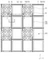
표시 영역(DA)은 제1 표시 영역(DA1) 및 제2 표시 영역(DA)을 포함한다. 제2 표시 영역(DA2)은 영상을 표시하는 고유의 기능 외에 다른 기능을 할 수 있도록 제1 표시 영역(DA1)보다 높은 투과율을 가진다. 여기서 투과율은 표시 패널(10)을 제3 방향(z)으로 투과하는 광의 투과율을 의미한다. 광은 가시광 및/또는 가시광 외의 파장의 광(예컨대, 적외광)일 수 있다. 제2 표시 영역(DA2)은 제1 표시 영역(DA1)보다 화소(PX)의 밀도, 즉 단위 면적당 화소(PX)의 개수가 작다.The display area (DA) includes a first display area (DA1) and a second display area (DA). The second display area (DA2) has higher transmittance than the first display area (DA1) so that it can perform other functions in addition to its own function of displaying an image. Here, the transmittance means the transmittance of light that transmits the display panel (10) in a third direction (z). The light may be visible light and/or light of a wavelength other than visible light (e.g., infrared light). The second display area (DA2) has a lower pixel (PX) density, that is, a lower number of pixels (PX) per unit area, than the first display area (DA1).
표시 영역(DA)에서 제2 표시 영역(DA2)은 다양하게 배치될 수 있다. 도시된 실시예에서, 제2 표시 영역(DA2)은 제1 표시 영역(DA1) 내에 위치하고 제1 표시 영역(DA1)에 의해 둘러싸여 있다. 제2 표시 영역(DA2)은 비표시 영역(NA)에 접하여 위치할 수 있다. 제2 표시 영역(DA2)은 표시 영역(DA)의 상단에서 좌측, 우측 및/또는 중앙에 위치할 수 있다. 제2 표시 영역(DA2)은 2개 이상의 영역으로 분리되어 위치할 수 있다. 제2 표시 영역(DA2)은 표시 영역(DA)의 상단을 완전히 가로질러 제1 방향(x)을 따라 위치할 수 있다. 제2 표시 영역(DA2)은 표시 영역(DA)의 좌측단 및/또는 우측단을 가로질러 제2 방향(y)을 따라 위치할 수 있다. 제2 표시 영역(DA2)은 사각형, 삼각형 등의 다각형, 원형, 타원형 등 다양한 형상을 가질 수 있다.The second display area (DA2) in the display area (DA) can be arranged in various ways. In the illustrated embodiment, the second display area (DA2) is located within the first display area (DA1) and is surrounded by the first display area (DA1). The second display area (DA2) can be located in contact with the non-display area (NA). The second display area (DA2) can be located at the left, right, and/or center of the top of the display area (DA). The second display area (DA2) can be divided into two or more areas. The second display area (DA2) can be located along the first direction (x) so as to completely cross the top of the display area (DA). The second display area (DA2) can be located along the second direction (y) so as to cross the left end and/or the right end of the display area (DA). The second display area (DA2) can have various shapes such as a polygon such as a square or a triangle, a circle, an oval, etc.
표시 패널(10)의 비표시 영역(NA)에는 표시 패널(10)을 구동하기 위한 각종 신호를 생성 및/또는 처리하는 구동 장치(driving unit)가 위치할 수 있다. 구동 장치는 데이터선들에 데이터 전압을 인가하는 데이터 구동부(data driver), 게이트선들에 게이트 신호를 인가하는 게이트 구동부(gate driver), 데이터 구동부 및 게이트 구동부를 제어하는 신호 제어부(signal controller) 등을 포함할 수 있다. 게이트 구동부는 표시 패널(10)에 집적될 수 있고, 표시 영역(DA)의 좌우 양측 또는 일측에 위치할 수 있다. 데이터 구동부 및 신호 제어부는 집적회로 칩(구동 IC 칩이라고도 함)(30)으로 제공될 수 있고, 집적회로 칩(30)은 연성 인쇄 회로막(20)에 실장되어 표시 패널(10)에 전기적으로 연결될 수 있다. 집적회로 칩(30)은 표시 패널(10)의 비표시 영역(NA)에 실장될 수도 있다.A driving unit that generates and/or processes various signals for driving the display panel (10) may be located in the non-display area (NA) of the display panel (10). The driving unit may include a data driver that applies a data voltage to data lines, a gate driver that applies a gate signal to gate lines, a signal controller that controls the data driver and the gate driver, etc. The gate driver may be integrated into the display panel (10) and may be located on either the left or right sides or one side of the display area (DA). The data driver and the signal controller may be provided as an integrated circuit chip (also referred to as a driving IC chip) (30), and the integrated circuit chip (30) may be mounted on a flexible printed circuit film (20) and electrically connected to the display panel (10). The integrated circuit chip (30) may also be mounted in the non-display area (NA) of the display panel (10).
터치를 감지할 수 있는 터치 감지 영역(TSA)은 표시 영역(DA)과 대략 일치할 수 있다. 터치 감지 영역(TSA)에는 터치 전극들(TE)이 배열되어 있다. 하나의 터치 전극(TE)은 다수의 화소(PX)에 걸쳐 있을 수 있다. 터치 전극들(TE)은 사용자의 접촉 또는 비접촉 터치를 감지할 수 있다. 각각의 터치 전극(TE)이 자기 축전기(self-capacitor) 방식으로 터치를 감지하거나, 인접하는 터치 전극들(TE)이 상호 축전기(mutual capacitor) 방식으로 터치를 감지할 수 있다. 표시 패널(10)은 터치 스크린 패널로 불릴 수 있다. 표시 장치(1)는 터치 전극들(TE)을 구동하기 위한 신호들을 생성하고 터치 전극들(TE)로부터 수신된 신호들을 처리하는 터치 구동부를 포함할 수 있고, 터치 구동부는 집적회로 칩으로 제공될 수 있다.A touch sensing area (TSA) capable of detecting a touch may roughly coincide with a display area (DA). Touch electrodes (TE) are arranged in the touch sensing area (TSA). One touch electrode (TE) may span a plurality of pixels (PX). The touch electrodes (TE) may detect a user's contact or non-contact touch. Each touch electrode (TE) may detect a touch in a self-capacitor manner, or adjacent touch electrodes (TE) may detect a touch in a mutual capacitor manner. The display panel (10) may be called a touch screen panel. The display device (1) may include a touch driver that generates signals for driving the touch electrodes (TE) and processes signals received from the touch electrodes (TE), and the touch driver may be provided as an integrated circuit chip.
표시 패널(10)은 기판(SB)을 포함할 수 있고, 기판(SB) 위에 화소들(PX)이 형성될 수 있다. 기판(SB)은 제1 표시 영역(DA1)과 제2 표시 영역(DA2)에 걸쳐 연속적으로 위치할 수 있다. 표시 패널(10)은 화소들(PX)을 전체적으로 덮는 봉지층(EN)을 포함할 수 있다. 봉지층(EN)은 제1 표시 영역(DA1) 및 제2 표시 영역(DA2)을 밀봉하여 표시 패널(10) 내부로 수분이나 산소가 침투하는 것을 막을 수 있다.The display panel (10) may include a substrate (SB), and pixels (PX) may be formed on the substrate (SB). The substrate (SB) may be positioned continuously across a first display area (DA1) and a second display area (DA2). The display panel (10) may include an encapsulation layer (EN) that entirely covers the pixels (PX). The encapsulation layer (EN) may seal the first display area (DA1) and the second display area (DA2) to prevent moisture or oxygen from penetrating into the display panel (10).
봉지층(EN) 위에는 터치 전극들(TE)이 배열되어 있는 터치 센서층(TS)이 위치할 수 있다. 터치 전극(TE)은 메탈 메시(metal mesh)로 구성될 수 있다. 터치 전극(TE)은 인듐 주석 산화물(ITO), 인듐 아연 산화물(IZO) 같은 투명 도전 물질로 형성될 수도 있다. 터치 전극(TE)은 단층 또는 복층으로 형성될 수 있다.A touch sensor layer (TS) having touch electrodes (TE) arranged thereon may be positioned on the encapsulation layer (EN). The touch electrode (TE) may be composed of a metal mesh. The touch electrode (TE) may be formed of a transparent conductive material such as indium tin oxide (ITO) or indium zinc oxide (IZO). The touch electrode (TE) may be formed as a single layer or multiple layers.
터치 센서층(TS) 위에는 외광 반사를 줄이기 위한 반사 방지층(AR)이 위치할 수 있고, 반사 방지층(AR)은 편광층 및/또는 위상 지연층을 포함할 수 있다.An anti-reflection layer (AR) may be positioned on the touch sensor layer (TS) to reduce external light reflection, and the anti-reflection layer (AR) may include a polarizing layer and/or a phase delay layer.
광학 장치(40)는 표시 패널(10)의 배면에 표시 패널(10)과 중첩하게 위치할 수 있다. 광학 장치(40)는 카메라, 센서, 플래시 등일 수 있다. 광학 장치(40)가 센서인 경우, 광학 장치(40)는 근접 센서 또는 조도 센서일 수 있다. 광학 장치(40)가 이용하는 파장의 광은 제2 표시 영역(DA2)을 통해 더 높은 투과율로 표시 패널(10)을 통과할 수 있다. 표시 패널(10)의 배면에는 광학 장치(40) 외에도 다양한 전자 장치가 위치할 수 있다.The optical device (40) may be positioned on the back surface of the display panel (10) to overlap the display panel (10). The optical device (40) may be a camera, a sensor, a flash, etc. When the optical device (40) is a sensor, the optical device (40) may be a proximity sensor or an illuminance sensor. Light of a wavelength used by the optical device (40) may pass through the display panel (10) with higher transmittance through the second display area (DA2). In addition to the optical device (40), various electronic devices may be positioned on the back surface of the display panel (10).
광학 장치(40)는 표시 패널(10)의 전면에 위치하는 물체(OB) 쪽으로 일정 파장 범위의 광(L)을 출사하거나 물체(OB)에서 반사되는 광(L)을 입사받을 수 있다. 이러한 일정 파장 범위의 광(L)은 광학 장치(40)에서 처리 가능한 파장의 광이고, 가시광 및/또는 적외광일 수 있다. 일정 파장의 광은 제2 표시 영역(DA2)에 위치하는 투과 영역을 주로 통과할 수 있다. 광학 장치(40)가 적외광을 사용하는 경우 일정 파장의 광은 약 900nm 내지 약 1000nm의 파장 영역을 가질 수 있다. 광학 장치(40)는 표시 패널(10)의 전면에 조사되는 일정 파장의 광을 입사받을 수도 있다. 광학 장치(40)는 제2 표시 영역(DA2) 전체에 대응하여 배치될 수 있고, 제2 표시 영역(DA2)의 일부에만 대응하여 배치될 수도 있다. 제2 표시 영역(DA2)에는 복수의 광학 장치(40)가 배치될 수도 있다.The optical device (40) can emit light (L) of a certain wavelength range toward an object (OB) positioned in front of the display panel (10) or receive light (L) reflected from the object (OB). The light (L) of this certain wavelength range is light of a wavelength that can be processed by the optical device (40) and may be visible light and/or infrared light. The light of a certain wavelength can mainly pass through a transmission area positioned in the second display area (DA2). When the optical device (40) uses infrared light, the light of a certain wavelength can have a wavelength range of about 900 nm to about 1000 nm. The optical device (40) can also receive light of a certain wavelength that is irradiated on the front of the display panel (10). The optical device (40) can be arranged to correspond to the entire second display area (DA2) or can be arranged to correspond to only a part of the second display area (DA2). A plurality of optical devices (40) can be arranged in the second display area (DA2).
도 3 및 도 4를 참고하여 일 실시예에 따른 표시 장치(1)의 제1 표시 영역(DA1) 및 제2 표시 영역(DA2)에 대해 설명한다.Referring to FIGS. 3 and 4, a first display area (DA1) and a second display area (DA2) of a display device (1) according to one embodiment will be described.
도 3 및 도 4는 일 실시예에 따른 표시 장치(1)의 제1 표시 영역(DA1)과 제2 표시 영역(DA2)의 개략적인 배치도이다. 도 3은 제1 및 제2 화소 영역(PA1, PA2)과 투과 영역(TA)의 개략적인 배치를 도시하고, 도 4는 제1 및 제2 화소 영역(PA1, PA2) 및 투과 영역(TA)이 포함할 수 있는 화소들(PX)을 좀더 구체화하여 도시한다.FIG. 3 and FIG. 4 are schematic layout diagrams of a first display area (DA1) and a second display area (DA2) of a display device (1) according to one embodiment. FIG. 3 schematically illustrates the layout of the first and second pixel areas (PA1, PA2) and the transparent area (TA), and FIG. 4 illustrates pixels (PX) that the first and second pixel areas (PA1, PA2) and the transparent area (TA) may include in more detail.
도 3을 참고하면, 제1 표시 영역(DA1)은 제1 화소 영역들(PA1)을 포함하고, 제2 표시 영역(DA2)은 제2 화소 영역들(PA2)과 투과 영역들(TA)을 포함한다. 하나의 제1 화소 영역(PA1)의 크기와 하나의 제2 화소 영역(PA2)의 크기는 동일할 수 있고, 다를 수도 있다.Referring to FIG. 3, the first display area (DA1) includes first pixel areas (PA1), and the second display area (DA2) includes second pixel areas (PA2) and transparent areas (TA). The size of one first pixel area (PA1) and the size of one second pixel area (PA2) may be the same or different.
제1 표시 영역(DA1)에서 제1 화소 영역들(PA1)은 제1 방향(x)과 제2 방향(y)으로 행렬로 배열될 수 있다. 제2 표시 영역(DA2)에서 제2 화소 영역들(PA2)과 투과 영역들(TA)이 행렬로 배열될 수 있다. 제1 방향(x) 및/또는 제2 방향(y)으로 하나 이상의 제2 화소 영역(PA2)과 하나 이상의 투과 영역(TA)이 교대로 배열될 수 있다. 제2 화소 영역들(PA2)과 투과 영역들(TA)이 고르게 혼재할 수 있도록, 제2 화소 영역들(PA2)과 투과 영역들(TA)은 체커보드(checkerboard) 패턴으로 배열될 수 있다. 도시된 실시예에서, 2개의 제2 화소 영역(PA2)을 투과 영역들(TA)이 둘러싸고 있다. 다른 예로, 1개의 제2 화소 영역(PA2)을 투과 영역들(TA)이 둘러싸도록 배열될 수도 있다.In the first display area (DA1), the first pixel areas (PA1) may be arranged in a matrix in the first direction (x) and the second direction (y). In the second display area (DA2), the second pixel areas (PA2) and the transparent areas (TA) may be arranged in a matrix. One or more second pixel areas (PA2) and one or more transparent areas (TA) may be alternately arranged in the first direction (x) and/or the second direction (y). In order for the second pixel areas (PA2) and the transparent areas (TA) to be evenly mixed, the second pixel areas (PA2) and the transparent areas (TA) may be arranged in a checkerboard pattern. In the illustrated embodiment, two second pixel areas (PA2) are surrounded by the transparent areas (TA). As another example, the transparent areas (TA) may be arranged to surround one second pixel area (PA2).
하나의 제2 화소 영역(PA2)의 크기와 하나의 투과 영역(TA)의 크기는 실질적으로 동일할 수 있고, 다를 수도 있다. 각각의 투과 영역(TA)은 크기가 실질적으로 동일할 수 있고, 다를 수도 있다. 제2 화소 영역들(PA2)과 투과 영역들(TA)의 배치 및 크기는 다양하게 변경될 수 있다. 예컨대, 제2 표시 영역(DA2)에서 투과 영역들(TA)은 도시된 실시예에서, 제2 화소 영역(PA2) 대 투과 영역(TA)의 면적 비가 대략 1:3이지만, 대략 1:1, 1:7, 1:15 등 다양한 면적 비로 배치될 수 있다. 예컨대, 제2 화소 영역(PA2) 대 투과 영역(TA)의 면적 비는 약 1:2n-1일 수 있다 (여기서 n은 자연수). 제2 화소 영역(PA2) 대 투과 영역(TA)의 비에 따라 제2 표시 영역(DA2)의 화소 밀도와 투과율이 변할 수 있다. 화소 밀도와 투과율은 트레이드오프(trade-off) 관계일 수 있다.The size of one second pixel area (PA2) and the size of one transparent area (TA) may be substantially the same or different. The size of each transparent area (TA) may be substantially the same or different. The arrangement and size of the second pixel areas (PA2) and the transparent areas (TA) may be variously changed. For example, in the illustrated embodiment, the transparent areas (TA) in the second display area (DA2) may be arranged at various area ratios, such as approximately 1:3 in the area ratio of the second pixel area (PA2) to the transparent area (TA), but approximately 1:1, 1:7, 1:15, etc. For example, the area ratio of the second pixel area (PA2) to the transparent area (TA) may be approximately 1:2n-1 (where n is a natural number). The pixel density and transmittance of the second display area (DA2) may vary depending on the ratio of the second pixel area (PA2) to the transparent area (TA). Pixel density and transmittance can be a trade-off.
제1 화소 영역(PA1) 및 제2 화소 영역(PA2)은 각각 하나 이상의 화소(PX)를 포함할 수 있다. 화소(PX)는 화소 회로 및 발광부를 포함할 수 있다. 화소 회로는 발광 다이오드(LED) 같은 발광 소자(light emitting element)를 구동하기 위한 회로로서 트랜지스터(transistor), 축전기 등을 포함할 수 있다. 발광부는 발광 소자에서 발광되는 광이 방출되는 영역이다. 도 4에 도시되는 화소(PX)는 발광부에 대응할 수 있다. 발광부는 마름모형일 수 있지만, 직사각형, 원형 등 다양한 형상을 가질 수 있다. 화소(PX)는 한 방향, 즉 제3 방향(z)으로 광을 방출할 수 있다. 제1 화소 영역(PA1) 및 제2 화소 영역(PA2)에는 터치 전극 섹션(TES)이 위치할 수 있다. 터치 전극 섹션(TES)은 금속선이 그물처럼 얽혀 있는 메탈 메시로 형성될 수 있고, 메탈 메시는 발광부를 가리지 않도록 위치할 수 있다. 복수의 터치 전극 섹션(TES)은 서로 연결되어 하나의 터치 전극(TE)을 구성할 수 있다.The first pixel area (PA1) and the second pixel area (PA2) may each include one or more pixels (PX). The pixel PX may include a pixel circuit and a light emitting unit. The pixel circuit is a circuit for driving a light emitting element such as a light emitting diode (LED) and may include a transistor, a capacitor, and the like. The light emitting unit is an area where light emitted from the light emitting element is emitted. The pixel PX illustrated in FIG. 4 may correspond to the light emitting unit. The light emitting unit may be diamond-shaped, but may have various shapes such as a rectangle or a circle. The pixel PX may emit light in one direction, that is, a third direction (z). A touch electrode section (TES) may be positioned in the first pixel area (PA1) and the second pixel area (PA2). The touch electrode section (TES) may be formed of a metal mesh in which metal lines are intertwined like a net, and the metal mesh may be positioned so as not to cover the light emitting unit. A plurality of touch electrode sections (TES) can be connected to each other to form a single touch electrode (TE).
투과 영역(TA)은 회소 회로와 발광부를 포함하지 않는다. 터치 전극(TE)은 투과 영역(TA)에 위치하지 않거나, 거의 위치하지 않을 수 있다. 터치 전극(TE)은 공통 전극(E2)의 개구(OPN)와 중첩하지 않을 수 있다. 투과 영역(TA)에는 광의 투과를 방해하는 화소 회로, 발광부, 터치 전극(TE) 등이 위치하지 않거나, 거의 위치하지 않으므로, 제1 및 제2 화소 영역들(PA1, PA2)보다 투과율이 높다. 도시된 것과 달리, 제2 표시 영역(DA2)에서 터치 전극(TE)은 제2 화소 영역(PA2)과 투과 영역(TA)에 걸쳐 연속적으로 위치할 수도 있다.The transparent area (TA) does not include a pixel circuit and a light-emitting portion. The touch electrode (TE) may not be positioned in the transparent area (TA), or may be hardly positioned therein. The touch electrode (TE) may not overlap with the opening (OPN) of the common electrode (E2). Since the pixel circuit, light-emitting portion, touch electrode (TE), etc., which obstruct the transmission of light, are not positioned in the transparent area (TA), or are hardly positioned therein, the transparent area (TA) has higher transmittance than the first and second pixel areas (PA1, PA2). Unlike what is illustrated, in the second display area (DA2), the touch electrode (TE) may be positioned continuously across the second pixel area (PA2) and the transparent area (TA).
도 4에 도시된 실시예에서, 각각의 제1 화소 영역(PA1)은 1개의 적색 화소(R), 2개의 녹색 화소(G) 및 1개의 청색 화소(B)를 포함한다. 각각의 제2 화소 영역(PA2)은 1개의 적색 화소(R), 2개의 녹색 화소(G) 및 1개의 청색 화소(B)를 포함한다. 도시된 것과 달리, 제1 화소 영역(PA1)의 화소 배치와 제2 화소 영역(PA2)의 화소 배치가 다를 수 있다. 각각의 화소 영역(PA1, PA2)이 포함하는 화소들(R, G, B)의 집합을 단위 화소라고 할 경우, 제1 화소 영역(PA1)의 단위 화소의 구성과 제2 화소 영역(PA2)의 단위 화소의 구성은 동일할 수 있고, 다를 수도 있다. 단위 화소는 1개의 적색 화소(R), 1개의 녹색 화소(G) 및 1개의 청색 화소(B)를 포함할 수 있다. 단위 화소는 적색 화소(R), 녹색 화소(G) 및 청색 화소(B) 중 적어도 하나를 포함할 수 있고, 백색 화소를 포함할 수도 있다.In the embodiment illustrated in FIG. 4, each first pixel area PA1 includes one red pixel R, two green pixels G, and one blue pixel B. Each second pixel area PA2 includes one red pixel R, two green pixels G, and one blue pixel B. Unlike what is illustrated, the pixel arrangement of the first pixel area PA1 and the pixel arrangement of the second pixel area PA2 may be different. When a set of pixels (R, G, B) included in each pixel area PA1 and PA2 is referred to as a unit pixel, the configuration of the unit pixel of the first pixel area PA1 and the configuration of the unit pixel of the second pixel area PA2 may be the same or different. The unit pixel may include one red pixel R, one green pixel G, and one blue pixel B. A unit pixel may include at least one of a red pixel (R), a green pixel (G), and a blue pixel (B), and may also include a white pixel.
제1 표시 영역(DA1)이 포함하는 화소들(R, G, B)은 제1 방향(x)으로 화소행(pixel row)을 이룬다. 제2 표시 영역(DA2)이 포함하는 화소들(R, G, B)도 제1 방향(x)으로 화소행을 이룬다.The pixels (R, G, B) included in the first display area (DA1) form a pixel row in the first direction (x). The pixels (R, G, B) included in the second display area (DA2) also form a pixel row in the first direction (x).
제1 표시 영역(DA1)에서 각각의 화소행에는 화소들(R, G, B)이 제1 방향(x)으로 대략 일렬로 배열되어 있다. 각각의 화소행에서 화소들(R, G, B)은 제1 방향(x)으로 적색 화소(R), 녹색 화소(G), 청색 화소(B) 및 녹색 화소(G) 순서로 반복적으로 배열될 수 있다. 하나의 화소행이 포함하는 화소들(R, G, B)의 배치는 다양하게 변경될 수 있다. 예컨대, 화소들(R, G, B)은 제1 방향(x)으로 청색 화소(B), 녹색 화소(G), 적색 화소(R) 및 녹색 화소(G) 순서로 반복적으로 배열되거나, 적색 화소(R), 청색 화소(B), 녹색 화소(G) 및 청색 화소(B) 순서로 반복적으로 배열될 수 있다.In the first display area (DA1), pixels (R, G, B) are arranged roughly in a single line in the first direction (x) in each pixel row. In each pixel row, the pixels (R, G, B) may be repeatedly arranged in the order of a red pixel (R), a green pixel (G), a blue pixel (B), and a green pixel (G) in the first direction (x). The arrangement of the pixels (R, G, B) included in one pixel row may be variously changed. For example, the pixels (R, G, B) may be repeatedly arranged in the order of a blue pixel (B), a green pixel (G), a red pixel (R), and a green pixel (G) in the first direction (x), or may be repeatedly arranged in the order of a red pixel (R), a blue pixel (B), a green pixel (G), and a blue pixel (B).
제2 표시 영역(DA2)에서 각각의 화소행에는 화소들(R, G, B)이 제1 방향(x)으로 대략 일렬로 배열되어 있다. 각각의 화소행에서 화소들(R, G, B)은 제1 방향(x)으로 적색 화소(R), 녹색 화소(G), 청색 화소(B) 및 녹색 화소(G) 순서로 반복적으로 배열될 수 있다. 하나의 화소행이 포함하는 화소들(R, G, B)의 배치는 다양하게 변경될 수 있다.In the second display area (DA2), pixels (R, G, B) are arranged roughly in a single line in the first direction (x) in each pixel row. In each pixel row, pixels (R, G, B) can be repeatedly arranged in the order of red pixel (R), green pixel (G), blue pixel (B), and green pixel (G) in the first direction (x). The arrangement of pixels (R, G, B) included in one pixel row can be changed in various ways.
제1 및 제2 화소 영역(PA1, PA2)의 화소들(R, G, B)은 또한 제2 방향(y)으로 화소열(pixel column)을 이룬다. 각각의 화소열에는 화소들(R, G, B)이 제2 방향(y)으로 대략 일렬로 배열되어 있다. 각각의 화소열에는 동일 색상의 화소들(PX)이 배치될 수 있고, 2색 이상의 화소들(PX)이 제2 방향(y)으로 번갈아 가며 배치될 수도 있다. 하나의 화소열이 포함하는 화소들(R, G, B)의 배치는 다양하게 변경될 수 있다.The pixels (R, G, B) of the first and second pixel areas (PA1, PA2) also form pixel columns in the second direction (y). In each pixel column, the pixels (R, G, B) are arranged approximately in a single line in the second direction (y). In each pixel column, pixels (PX) of the same color may be arranged, and pixels (PX) of two or more colors may be arranged alternately in the second direction (y). The arrangement of the pixels (R, G, B) included in one pixel column may be variously changed.
제2 화소 영역(PA2)의 화소들(R, G, B)은 단면 발광형, 예컨대 제3 방향(z)으로 발광하는 전면 발광형일 수 있다. 제2 화소 영역(PA2)의 화소들(R, G, B)은 배면 발광형이거나, 양면 발광형일 수도 있다.The pixels (R, G, B) of the second pixel area (PA2) may be cross-sectional emission type, for example, a top emission type that emits light in the third direction (z). The pixels (R, G, B) of the second pixel area (PA2) may be a back emission type or a double-sided emission type.
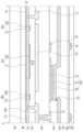
도 5는 도 4에서 A 영역의 개략적인 확대도이고, 도 6은 도 5에서 A-A'선을 따라 취한 개략적인 단면도이고, 도 7은 도 5에서 B-B'선을 따라 취한 개략적인 단면도이다. 도 5는 제2 표시 영역(DA2)에서 대략 8개의 제2 화소 영역(PA2) 및 24개의 투과 영역(TA)을 도시한다. 도 6은 제2 화소 영역(PA2)에 위치하는 화소 회로(PC)의 구성 중 하나의 트랜지스터(TR)와 하나의 축전기(CP)를 개략적으로 도시한다.FIG. 5 is a schematic enlarged view of area A in FIG. 4, FIG. 6 is a schematic cross-sectional view taken along line A-A' in FIG. 5, and FIG. 7 is a schematic cross-sectional view taken along line B-B' in FIG. 5. FIG. 5 illustrates approximately eight second pixel areas (PA2) and twenty-four transmission areas (TA) in a second display area (DA2). FIG. 6 schematically illustrates one transistor (TR) and one capacitor (CP) among the components of a pixel circuit (PC) located in the second pixel area (PA2).
도 5를 참고하면, 제2 표시 영역(DA2)에서 제2 화소 영역(PA2)과 투과 영역(TA)은 인접하고, 제2 화소 영역(PA2)은 화소들(R, G, B)을 포함한다. 화소들(R, G, B)에 게이트 신호를 전달하는 게이트선(GL1, GL2)은 대략 제1 방향(x)으로 연장할 수 있고, 데이터 신호를 전달하는 데이터선(DL)은 대략 제2 방향(y)으로 연장할 수 있다. 각각의 화소열에는 하나의 데이터선(DL)이 제공될 수 있다. 각각의 데이터선(DL)은 제1 표시 영역(DA1) 및 제2 표시 영역(DA2)에 걸쳐 연장할 수 있다. 각각의 화소행에는 서로 다른 타이밍의 게이트 온 전압을 전달할 수 있다 2개 이상의 게이트선(GL1, GL2)이 제공될 수 있다. 도시된 것과 달리, 각각의 화소열에 복수의 데이터선(DL)이 제공되거나, 복수의 화소열에 하나의 데이터선(DL)이 제공될 수도 있다.Referring to FIG. 5, in the second display area (DA2), the second pixel area (PA2) and the transparent area (TA) are adjacent, and the second pixel area (PA2) includes pixels (R, G, B). Gate lines (GL1, GL2) for transmitting gate signals to the pixels (R, G, B) may extend approximately in a first direction (x), and data lines (DL) for transmitting data signals may extend approximately in a second direction (y). One data line (DL) may be provided for each pixel column. Each data line (DL) may extend across the first display area (DA1) and the second display area (DA2). Two or more gate lines (GL1, GL2) for transmitting gate-on voltages of different timings may be provided for each pixel row. Unlike what is illustrated, a plurality of data lines (DL) may be provided for each pixel column, or a single data line (DL) may be provided for a plurality of pixel columns.
게이트선(GL1, GL2) 및 데이터선(DL)에 의해 투과 영역(TA)의 투과율이 저하되지 않도록, 게이트선(GL1, GL2) 및 데이터선(DL)은 인접하는 투과 영역들(TA)의 대략 경계를 지나도록 연장할 수 있다. 도시된 실시예에서, 인접하는 두 데이터선(DL) 중 하나는 제2 화소 영역(PA2)과 투과 영역(TA)의 대략 경계 부근에서 제1 방향(x)으로 연장하는 부분을 포함하고, 인접하는 두 게이트선(GL1, GL2) 중 하나는 제2 화소 영역(PA2)과 투과 영역(TA)의 대략 경계 부근에서 제2 방향(y)으로 연장하는 부분을 포함한다. 게이트선(GL1, GL2) 및 데이터선(DL)은 제2 화소 영역(PA2)과 투과 영역(TA)의 대략 경계를 지나도록 연장하거나, 제2 화소 영역(PA2)을 지나도록 연장할 수 있다.In order to prevent the transmittance of the transparent area (TA) from being lowered by the gate lines (GL1, GL2) and the data line (DL), the gate lines (GL1, GL2) and the data line (DL) can extend to roughly pass through the boundaries of the adjacent transparent areas (TA). In the illustrated embodiment, one of the two adjacent data lines (DL) includes a portion extending in the first direction (x) near the boundary between the second pixel area (PA2) and the transparent area (TA), and one of the two adjacent gate lines (GL1, GL2) includes a portion extending in the second direction (y) near the boundary between the second pixel area (PA2) and the transparent area (TA). The gate lines (GL1, GL2) and the data line (DL) can extend to roughly pass through the boundary between the second pixel area (PA2) and the transparent area (TA), or can extend to pass through the second pixel area (PA2).
도 5, 도 6 및 도 7을 참고하면, 표시 장치는 기판(SB) 및 그 위에 형성된 여러 층, 배선, 소자를 포함한다. 소자들은 트랜지스터(TR), 축전기(CP), 발광 다이오드(LED)를 포함할 수 있다.Referring to FIGS. 5, 6, and 7, the display device includes a substrate (SB) and several layers, wiring, and elements formed thereon. The elements may include a transistor (TR), a capacitor (CP), and a light-emitting diode (LED).
기판(SB)은 폴리이미드(polyimide), 폴리아미드(polyamide) 같은 폴리머 또는 유리 등의 절연 물질을 포함할 수 있고 광학적으로 투명할 수 있다. 기판(SB)이 폴리머층을 포함하는 경우, 기판(SB)은 수분 등의 침투를 방지하기 위해 규소 산화물(SiOx), 규소 질화물(SiNx) 같은 무기 절연 물질을 포함하는 배리어층(barrier layer)을 포함할 수 있다.The substrate (SB) may include a polymer such as polyimide or polyamide, or an insulating material such as glass, and may be optically transparent. When the substrate (SB) includes a polymer layer, the substrate (SB) may include a barrier layer including an inorganic insulating material such as silicon oxide (SiOx ) or silicon nitride (SiNx ) to prevent penetration of moisture, etc.
기판(SB) 위에는 액티브층(active layer)(AL)의 특성을 열화시키는 불순물이 확산되는 것을 방지하고 수분 등의 침투를 방지하기 위한 버퍼층(buffer layer)(BF)이 위치할 수 있다.A buffer layer (BF) may be positioned on the substrate (SB) to prevent diffusion of impurities that deteriorate the characteristics of the active layer (AL) and to prevent penetration of moisture, etc.
버퍼층(BF) 위에는 트랜지스터(TR)의 액티브층(AL)이 위치할 수 있다. 액티브층(AL)은 채널 영역(channel region)과 그 양측의 소스 영역 및 드레인 영역을 포함할 수 있다. 액티브층(AL)은 다결정 규소, 비정질 규소, 산화물 반도체 같은 반도체 물질을 포함할 수 있다.An active layer (AL) of a transistor (TR) may be positioned on the buffer layer (BF). The active layer (AL) may include a channel region and source and drain regions on both sides thereof. The active layer (AL) may include a semiconductor material such as polycrystalline silicon, amorphous silicon, or an oxide semiconductor.
액티브층(AL) 위에는 무기 절연 물질을 포함할 수 있는 제1 절연층(IN1)이 위치할 수 있다. 제1 절연층(IN1)은 기판(SB)의 전면에 걸쳐 위치할 수 있고, 투과 영역(TA)에도 위치할 수 있다.A first insulating layer (IN1) that may include an inorganic insulating material may be positioned on the active layer (AL). The first insulating layer (IN1) may be positioned over the entire surface of the substrate (SB) and may also be positioned in the transmission area (TA).
제1 절연층(IN1) 위에는 트랜지스터(TR)의 게이트 전극(GE), 축전기(CP)의 제1 전극(CE1), 게이트선(GL1, GL2) 등을 포함할 수 있는 제1 도전층이 위치할 수 있다. 게이트 전극(GE)은 액티브층(AL)의 채널 영역과 중첩할 수 있다. 제1 도전층은 몰리브덴(Mo), 구리(Cu), 알루미늄(Al), 은(Ag), 크롬(Cr), 탄탈륨(Ta), 티타늄(Ti) 등의 금속을 포함할 수 있다.A first conductive layer may be positioned on the first insulating layer (IN1), which may include a gate electrode (GE) of a transistor (TR), a first electrode (CE1) of a capacitor (CP), gate lines (GL1, GL2), etc. The gate electrode (GE) may overlap a channel region of the active layer (AL). The first conductive layer may include a metal such as molybdenum (Mo), copper (Cu), aluminum (Al), silver (Ag), chromium (Cr), tantalum (Ta), or titanium (Ti).
제1 도전층 위에는 무기 절연 물질을 포함할 수 있는 제2 절연층(IN2)이 위치할 수 있다. 제2 절연층(IN2) 위에는 트랜지스터(TR)의 소스 전극(SE) 및 드레인 전극(DE), 축전기(CP)의 제2 전극(CE2), 데이터선(DL), 구동 전압선 등을 포함할 수 있는 제2 도전층이 위치할 수 있다. 소스 전극(SE) 및 드레인 전극(DE)은 제2 절연층(IN2)의 개구들(openings)을 통해 액티브층(AL)의 소스 영역 및 드레인 영역에 각각 연결될 수 있다. 제2 도전층은 알루미늄(Al), 구리(Cu), 은(Ag), 금(Au), 백금(Pt), 팔라듐(Pd), 니켈(Ni), 몰리브덴(Mo), 텅스텐(W), 티타늄(Ti), 크롬(Cr), 탄탈륨(Ta) 등의 금속을 포함할 수 있다.A second insulating layer (IN2) that may include an inorganic insulating material may be positioned on the first conductive layer. A second conductive layer that may include a source electrode (SE) and a drain electrode (DE) of a transistor (TR), a second electrode (CE2) of a capacitor (CP), a data line (DL), a driving voltage line, etc. may be positioned on the second insulating layer (IN2). The source electrode (SE) and the drain electrode (DE) may be connected to a source region and a drain region of an active layer (AL), respectively, through openings in the second insulating layer (IN2). The second conductive layer may include a metal such as aluminum (Al), copper (Cu), silver (Ag), gold (Au), platinum (Pt), palladium (Pd), nickel (Ni), molybdenum (Mo), tungsten (W), titanium (Ti), chromium (Cr), or tantalum (Ta).
게이트 전극(GE), 소스 전극(SE) 및 드레인 전극(DE)은 액티브층(AL)과 함께 트랜지스터(TR)를 이룬다. 제1 전극(CE1) 및 제2 전극(CE2)은 이들 사이의 제2 절연층(IN2)과 함께 축전기(CP)를 이룬다. 화소 회로를 구성하는 이러한 트랜지스터(TR) 및 축전기(CP)는 투과 영역(TA)에는 위치하지 않을 수 있다.A gate electrode (GE), a source electrode (SE), and a drain electrode (DE) form a transistor (TR) together with an active layer (AL). A first electrode (CE1) and a second electrode (CE2) form a capacitor (CP) together with a second insulating layer (IN2) therebetween. These transistors (TR) and capacitors (CP) constituting the pixel circuit may not be located in the transmission area (TA).
제2 절연층(IN2) 및 제2 도전층 위에는 유기 절연 물질을 포함할 수 있는 제3 절연층(IN3)이 위치할 수 있다. 제3 절연층(IN3)은 그 위에 형성될 발광 소자의 발광 효율을 높이기 위해 단차를 없애고 평탄화하는 역할을 할 수 있다. 제3 절연층(IN3)은 제2 화소 영역(PA2)에서 제2 절연층(IN2) 및 제2 도전층을 덮도록 위치할 수 있다. 제3 절연층(IN3)은 트랜지스터(TR)를 덮고 있을 수 있다.A third insulating layer (IN3) that may include an organic insulating material may be positioned on the second insulating layer (IN2) and the second conductive layer. The third insulating layer (IN3) may serve to eliminate steps and provide a flat surface to increase the light-emitting efficiency of a light-emitting element to be formed thereon. The third insulating layer (IN3) may be positioned to cover the second insulating layer (IN2) and the second conductive layer in the second pixel area (PA2). The third insulating layer (IN3) may cover the transistor (TR).
제3 절연층(IN3)은 투과 영역(TA)에서는 투과율 향상을 위해 적어도 부분적으로 제거될 수 있다. 예컨대, 투과 영역(TA)과 제2 화소 영역(PA2)의 경계 부근 및 인접하는 투과 영역들(TA)의 경계 부근을 제외하고는 투과 영역(TA)에 위치하지 않을 수 있다.The third insulating layer (IN3) may be at least partially removed in the transparent area (TA) to improve transmittance. For example, it may not be located in the transparent area (TA) except near the boundary between the transparent area (TA) and the second pixel area (PA2) and near the boundary between adjacent transparent areas (TA).
제3 절연층(IN3) 위에는 화소 전극(E1)이 위치할 수 있다. 화소 전극(E1)은 화소(PX)의 발광 다이오드(LED)의 두 전극 중 제1 전극이다. 화소 전극(E1)은 제3 절연층(IN3)의 개구를 통해 트랜지스터(TR)의 드레인 전극(DE)과 연결될 수 있다. 화소 전극(E1)은 화소(PX)마다 개별적으로 제공될 수 있다. 화소 전극(E1)은 은(Ag), 리튬(Li), 칼슘(Ca), 알루미늄(Al), 마그네슘(Mg), 금(Au) 같은 금속을 포함할 수 있고, 인듐 주석 산화물(ITO), 인듐 아연 산화물(IZO) 같은 투명 도전성 산화물(TCO)을 포함할 수도 있다.A pixel electrode (E1) may be positioned on the third insulating layer (IN3). The pixel electrode (E1) is a first electrode of two electrodes of a light emitting diode (LED) of the pixel (PX). The pixel electrode (E1) may be connected to a drain electrode (DE) of a transistor (TR) through an opening in the third insulating layer (IN3). The pixel electrode (E1) may be individually provided for each pixel (PX). The pixel electrode (E1) may include a metal such as silver (Ag), lithium (Li), calcium (Ca), aluminum (Al), magnesium (Mg), or gold (Au), and may also include a transparent conductive oxide (TCO) such as indium tin oxide (ITO) or indium zinc oxide (IZO).
제3 절연층(IN3) 및 화소 전극(E1) 위에는 유기 절연 물질을 포함할 수 있는 제4 절연층(IN4)이 위치할 수 있다. 제4 절연층(IN4)은 화소 전극(E1)과 중첩하는 개구(OP)를 가질 수 있다. 개구(OP)는 화소(PX)의 발광부에 대응하는 영역을 한정할 수 있다. 제4 절연층(IN4)은 화소 전극(E1)의 가장자리를 덮고 있을 수 있다. 제3 절연층(IN3)과 유사하게, 제4 절연층(IN4)은 투과 영역(TA)에서는 투과율 향상을 위해 적어도 부분적으로 제거될 수 있다.A fourth insulating layer (IN4) that may include an organic insulating material may be positioned on the third insulating layer (IN3) and the pixel electrode (E1). The fourth insulating layer (IN4) may have an opening (OP) that overlaps the pixel electrode (E1). The opening (OP) may define an area corresponding to a light-emitting portion of the pixel (PX). The fourth insulating layer (IN4) may cover an edge of the pixel electrode (E1). Similar to the third insulating layer (IN3), the fourth insulating layer (IN4) may be at least partially removed in a transparent area (TA) to improve transmittance.
도시된 것과 달리, 제3 절연층(IN3) 및 제4 절연층(IN4) 중 적어도 하나는 투과 영역(TA)에서 제거되지 않고, 기판(SB) 전체를 덮도록 위치할 수도 있다. 투과 영역(TA)의 투과율 향상을 위해, 버퍼층(BF), 제1 절연층(IN1) 및 제2 절연층(IN2) 중 적어도 하나가 투과 영역(TA)에서 적어도 부분적으로 제거될 수도 있다.Unlike the illustrated embodiment, at least one of the third insulating layer (IN3) and the fourth insulating layer (IN4) may be positioned so as to cover the entire substrate (SB) without being removed from the transmission area (TA). In order to improve the transmittance of the transmission area (TA), at least one of the buffer layer (BF), the first insulating layer (IN1), and the second insulating layer (IN2) may be at least partially removed from the transmission area (TA).
화소 전극(E1) 위에는 발광층(EL)이 위치할 수 있다. 발광층(EL)은 적색, 녹색 및 청색 등의 기본색의 광을 고유하게 내는 물질층을 포함할 수 있다. 발광층(EL)은 서로 다른 색의 광을 내는 복수의 물질층이 적층된 구조를 가질 수도 있다.An emitting layer (EL) may be positioned on the pixel electrode (E1). The emitting layer (EL) may include a material layer that uniquely emits light of primary colors such as red, green, and blue. The emitting layer (EL) may have a structure in which multiple material layers that emit light of different colors are laminated.
발광층(EL) 위에는 공통 전극(E2)이 위치할 수 있다. 공통 전극(E2)은 발광 다이오드(LED)의 두 전극 중 제2 전극이다. 도 5에서 음영 영역이 공통 전극(E2)이 위치하는 영역에 해당한다. 제2 표시 영역(DA2)에서, 공통 전극(E2)은 각각의 제2 화소 영역(PA2)을 덮도록 위치할 수 있다. 공통 전극(E2)은 투과 영역(TA)에서는 투과율 향상을 위해 적어도 부분적으로 제거될 수 있다. 즉, 공통 전극(E2)은 투과 영역(TA)과 중첩하는 개구(OPN)를 포함할 수 있다. 공통 전극(E2)은 제1 방향(x)으로 인접하는 제2 화소 영역(PA2)과 투과 영역(TA)의 대략 경계 부근에서 데이터선(DL)과 중첩하게 위치할 수 있다. 공통 전극(E2)은 제2 방향(y)으로 인접하는 제2 화소 영역(PA2)과 투과 영역(TA)의 대략 경계 부근에서 게이트선(GL1, GL2)과 중첩하게 위치할 수 있다. 공통 전극(E2)은 제1 방향(x)으로 인접하는 투과 영역들(TA)의 대략 경계 부근에서 데이터선(DL)과 중첩하게 위치할 수 있다. 공통 전극(E2)은 제2 방향(y)으로 인접하는 투과 영역들(TA)의 대략 경계 부근에서 게이트선(GL1, GL2)과 중첩하게 위치할 수 있다.A common electrode (E2) may be positioned on the light-emitting layer (EL). The common electrode (E2) is the second electrode of the two electrodes of the light-emitting diode (LED). In FIG. 5, the shaded area corresponds to the area where the common electrode (E2) is positioned. In the second display area (DA2), the common electrode (E2) may be positioned to cover each second pixel area (PA2). The common electrode (E2) may be at least partially removed in the transmissive area (TA) to improve transmittance. That is, the common electrode (E2) may include an opening (OPN) overlapping the transmissive area (TA). The common electrode (E2) may be positioned to overlap the data line (DL) near the approximate boundary between the second pixel area (PA2) and the transmissive area (TA) that are adjacent in the first direction (x). The common electrode (E2) may be positioned to overlap the gate lines (GL1, GL2) at an approximate boundary between the second pixel area (PA2) and the transparent area (TA) adjacent in the second direction (y). The common electrode (E2) may be positioned to overlap the data line (DL) at an approximate boundary between the transparent areas (TA) adjacent in the first direction (x). The common electrode (E2) may be positioned to overlap the gate lines (GL1, GL2) at an approximate boundary between the transparent areas (TA) adjacent in the second direction (y).
이와 같이 공통 전극(E2)이 데이터선(DL) 및 게이트선(GL1, GL2) 위에 이들과 중첩하게 위치함으로써, 데이터선(DL) 및 게이트선(GL1, GL2)을 통해 전달되는 데이터 신호 및 게이트 신호에 의해, 터치 전극(TE)이 영향을 받는 것을 방지하거나 줄일 수 있다. 데이터선(DL)을 충분히 차폐할 수 있도록 공통 전극(E2)은 제4 절연층(IN4)의 측면을 따라 투과 영역(TA)의 가장자리까지 연장할 수 있다. 공통 전극(E2)은 데이터선(DL)의 상면과 적어도 한 측면을 둘러쌀 수 있다.In this way, by positioning the common electrode (E2) overlapping the data line (DL) and the gate lines (GL1, GL2), the touch electrode (TE) can be prevented or reduced from being affected by the data signal and the gate signal transmitted through the data line (DL) and the gate lines (GL1, GL2). The common electrode (E2) can extend along the side of the fourth insulating layer (IN4) to the edge of the transparent area (TA) so as to sufficiently shield the data line (DL). The common electrode (E2) can surround the upper surface and at least one side surface of the data line (DL).
제1 표시 영역(DA1)에서 공통 전극(E2)은 제1 화소 영역들(PA1) 전체를 덮도록 위치할 수 있다. 따라서 공통 전극(E2)은 표시 영역(DA)에서 실질적으로 투과 영역(TA)을 제외한 영역을 덮도록 위치할 수 있다. 공통 전극(E2)은 모든 화소(PX)에 공통으로 제공될 수 있고 공통 전압(ELVSS)을 인가받을 수 있다. 공통 전극(E2)은 인듐 주석 산화물(ITO), 인듐 아연 산화물(IZO) 같은 투명 도전성 산화물(TCO)을 포함할 수 있다.In the first display area (DA1), the common electrode (E2) may be positioned to cover the entire first pixel areas (PA1). Accordingly, the common electrode (E2) may be positioned to cover substantially an area excluding the transparent area (TA) in the display area (DA). The common electrode (E2) may be commonly provided to all pixels (PX) and may receive a common voltage (ELVSS). The common electrode (E2) may include a transparent conductive oxide (TCO) such as indium tin oxide (ITO) and indium zinc oxide (IZO).
공통 전극(E2) 위에는 캐핑층(CPL)이 위치할 수 있다. 캐핑층(CPL)은 굴절률 조정을 통해 광 효율을 향상시킬 수 있다. 캐핑층(CPL)은 공통 전극(E2)을 전체적으로 덮도록 위치할 수 있다. 캐핑층(CPL)은 유기 절연 물질을 포함할 수 있고, 무기 절연 물질을 포함할 수도 있다.A capping layer (CPL) may be positioned on the common electrode (E2). The capping layer (CPL) may improve light efficiency by adjusting the refractive index. The capping layer (CPL) may be positioned to entirely cover the common electrode (E2). The capping layer (CPL) may include an organic insulating material or may include an inorganic insulating material.
제1 화소 영역(PA1) 및 제2 화소 영역(PA2)에서 화소 전극(E1), 발광층(EL) 및 공통 전극(E2)은 발광 다이오드(LED)인 발광 소자를 이룬다. 화소 전극(E1)은 정공 주입 전극인 애노드(anode)일 수 있고, 공통 전극(E2)은 전자 주입 전극인 캐소드(cathode)일 수 있다. 이와 반대로, 화소 전극(E1)이 캐소드일 수 있고 공통 전극(E2)은 애노드일 수도 있다. 발광 다이오드(LED)는 화소 전극(E1)이 반사성이고 공통 전극(E2)이 투과성일 수 있고, 발광 다이오드(LED)가 발광하는 광은 전면으로, 즉 제3 방향(z)으로 방출될 수 있다.In the first pixel area (PA1) and the second pixel area (PA2), the pixel electrode (E1), the light-emitting layer (EL), and the common electrode (E2) form a light-emitting element, which is a light-emitting diode (LED). The pixel electrode (E1) may be an anode, which is a hole-injecting electrode, and the common electrode (E2) may be a cathode, which is an electron-injecting electrode. Conversely, the pixel electrode (E1) may be a cathode, and the common electrode (E2) may be an anode. In the light-emitting diode (LED), the pixel electrode (E1) may be reflective, the common electrode (E2) may be transmissive, and light emitted by the light-emitting diode (LED) may be emitted toward the front, that is, in the third direction (z).
캐핑층(CPL) 위에는 봉지층(EN)이 위치할 수 있다. 봉지층(EN)은 캐핑층(CPL) 위에 적어도 하나의 무기층 및/또는 적어도 하나의 유기층이 적층된 박막 봉지층일 수 있다.An encapsulation layer (EN) may be positioned on the capping layer (CPL). The encapsulation layer (EN) may be a thin film encapsulation layer in which at least one inorganic layer and/or at least one organic layer is laminated on the capping layer (CPL).
봉지층(EN) 위에는 규소 질화물, 규소 산화물 같은 무기 절연 물질을 포함할 수 있는 버퍼층(TBF)이 위치할 수 있다.A buffer layer (TBF) may be positioned on the encapsulation layer (EN), which may include an inorganic insulating material such as silicon nitride or silicon oxide.
버퍼층(TBF) 위에는 터치 전극(TE)이 위치할 수 있다. 터치 전극(TE)은 알루미늄(Al), 구리(Cu), 티타늄(Ti), 몰리브덴(Mo), 은(Ag), 크롬(Cr), 니켈(Ni) 등의 금속을 포함할 수 있다. 터치 전극(TE)은 발광부와 중첩하는 개구를 가진 메시 형태일 수 있다. 터치 전극(TE)은 은 나노와이어(silver nanowire), 탄소 나노튜브(carbon nanotube) 등의 도전성 나노 물질을 포함할 수 있다. 터치 전극(TE)은 ITO, TZO 같은 투명 도전 물질을 포함할 수 있다.A touch electrode (TE) may be positioned on the buffer layer (TBF). The touch electrode (TE) may include a metal such as aluminum (Al), copper (Cu), titanium (Ti), molybdenum (Mo), silver (Ag), chromium (Cr), or nickel (Ni). The touch electrode (TE) may have a mesh shape with an opening overlapping the light-emitting portion. The touch electrode (TE) may include a conductive nanomaterial such as a silver nanowire or a carbon nanotube. The touch electrode (TE) may include a transparent conductive material such as ITO or TZO.
터치 전극(TE)은 터치 전극(TE)과 동일층 또는 다른 층에 위치하는 배선을 통해 터치 구동부와 전기적으로 연결될 수 있다. 제1 방향(x) 또는 제2 방향(y)으로 인접하는 터치 전극들(TE)은 터치 전극(TE)과 동일층 또는 다른 층에 위치하는 브리지(bridge)를 통해 전기적으로 연결될 수 있다. 제2 표시 영역(DA2)에서 제1 방향(x) 및/또는 제2 방향(y)으로 인접하는 터치 전극 섹션들(TES)은 연결선(TEC)에 의해 전기적으로 연결될 수 있다. 터치 전극 섹션들(TES)과 연결선들(TEC)은 터치 전극(TE)을 구성할 수 있다.The touch electrode (TE) can be electrically connected to the touch driving unit through a wiring positioned on the same layer as or a different layer from the touch electrode (TE). The touch electrodes (TE) adjacent in the first direction (x) or the second direction (y) can be electrically connected through a bridge positioned on the same layer or a different layer from the touch electrode (TE). The touch electrode sections (TES) adjacent in the first direction (x) and/or the second direction (y) in the second display area (DA2) can be electrically connected by a connection line (TEC). The touch electrode sections (TES) and the connection lines (TEC) can form the touch electrode (TE).
제3 방향(z)으로 터치 전극(TE)과 데이터선(DL) 사이에는 이들과 중첩하는 발광 다이오드(LED)의 공통 전극(E2)이 위치한다. 따라서 공통 전극(E2)은 데이터선(DL) 및/또는 게이트선(GL1, GL2)으로부터 터치 전극(TE)으로 유입될 수 있는 노이즈를 차폐할 수 있다. 이에 따라, 터치 전극(TE)이 발광 다이오드(LED)의 구동을 위한 데이터 신호 및/또는 게이트 신호에 의해 영향을 받는 것을 방지할 수 있고, 터치 감도가 저하되는 문제를 개선할 수 있다.A common electrode (E2) of a light-emitting diode (LED) overlapping with the touch electrode (TE) and the data line (DL) is positioned between the touch electrode (TE) and the data line (DL) in the third direction (z). Therefore, the common electrode (E2) can shield noise that may be introduced from the data line (DL) and/or the gate lines (GL1, GL2) to the touch electrode (TE). Accordingly, the touch electrode (TE) can be prevented from being affected by the data signal and/or the gate signal for driving the light-emitting diode (LED), and the problem of reduced touch sensitivity can be improved.
또한, 공통 전극(E2)이 터치 전극(TE)과 중첩함에 따라 터치 전극(TE)과 공통 전극(E2)에 의해 형성되는 축전기의 용량이 증가할 수 있다. 터치 전극(TE)의 기본 정전 용량(base capacitance)이 증가하므로, 터치 전극(TE)이 자기 축전기 방식의 터치 터치 전극(TE)으로 사용되는 경우 터치 감도를 향상시킬 수 있다.In addition, as the common electrode (E2) overlaps the touch electrode (TE), the capacitance of the capacitor formed by the touch electrode (TE) and the common electrode (E2) can increase. Since the base capacitance of the touch electrode (TE) increases, when the touch electrode (TE) is used as a magnetic capacitor type touch electrode (TE), the touch sensitivity can be improved.
터치 전극(TE) 위에는 절연층(TIL)이 위치하여, 터치 전극(TE)을 보호할 수 있다.An insulating layer (TIL) is positioned on the touch electrode (TE) to protect the touch electrode (TE).
한편, 제1 표시 영역(DA1)의 제1 화소 영역(PA1)의 단면 구조는 제2 화소 영역(PA2)의 단면 구조에 대응할 수 있다.Meanwhile, the cross-sectional structure of the first pixel area (PA1) of the first display area (DA1) can correspond to the cross-sectional structure of the second pixel area (PA2).
이하, 몇몇 변형 가능한 실시예에 대해 전술한 실시예와 차이점을 위주로 설명한다.Below, some possible modified embodiments will be described with a focus on the differences from the above-described embodiments.
도 8 및 도 9는 일 실시예에 따른 표시 장치에서 도 4의 A 영역에 대응하는 영역의 개략적인 평면도이다.FIGS. 8 and 9 are schematic plan views of an area corresponding to area A of FIG. 4 in a display device according to one embodiment.
도 8의 실시예는 발광 다이오드(LED)의 공통 전극(E2)의 영역에 있어 도 5의 실시예와 차이가 있다. 도 8을 참고하면, 공통 전극(E2)은 제2 방향(y)으로 인접하는 투과 영역들(TA) 사이에는 위치하지 않는다.The embodiment of Fig. 8 differs from the embodiment of Fig. 5 in the area of the common electrode (E2) of the light emitting diode (LED). Referring to Fig. 8, the common electrode (E2) is not located between the transmission areas (TA) adjacent in the second direction (y).
게이트선(GL1, GL2)을 통해 인가되는 게이트 신호와 데이터선(DL)을 통해 인가되는 데이터 신호는 일정하지 않고 변동한다. 따라서 만약 터치 전극(TE)을 게이트선(GL1, GL2) 및/또는 데이터선(DL)으로부터 차폐하지 않으면, 터치 전극(TE)의 전압이 게이트 신호 및/또는 데이터 신호의 변동에 영향을 받을 수 있다. 게이트선(GL1, GL2)은 데이터선(DL)보다 터치 전극(TE)과의 거리가 멀기 때문에 (도 6 참고), 게이트선(GL1, GL2)이 터치 전극(TE)에 미치는 영향은 데이터선(DL)이 터치 전극(TE)에 미치는 영향보다 작다. 따라서 게이트선(GL1, GL2)이 제1 방향(x)으로 연장할 수 있는 투과 영역들(TA)의 경계 부근에서 공통 전극(E2)을 제거하여, 투과 영역(TA)의 투과율을 좀더 높일 수 있다.The gate signal applied through the gate lines (GL1, GL2) and the data signal applied through the data line (DL) are not constant but fluctuate. Therefore, if the touch electrode (TE) is not shielded from the gate lines (GL1, GL2) and/or the data line (DL), the voltage of the touch electrode (TE) may be affected by the fluctuations of the gate signal and/or the data signal. Since the gate lines (GL1, GL2) are further from the touch electrode (TE) than the data line (DL) (see FIG. 6), the influence of the gate lines (GL1, GL2) on the touch electrode (TE) is smaller than the influence of the data line (DL) on the touch electrode (TE). Therefore, by removing the common electrode (E2) near the boundary of the transparent areas (TA) in which the gate lines (GL1, GL2) can extend in the first direction (x), the transmittance of the transparent areas (TA) can be further increased.
이와 같이, 공통 전극(E2)이 형성된 영역을 축소할 수 있고, 반대로 확장할 수도 있다. 또한, 도 9에 도시된 바와 같이, 공통 전극(E2)의 영역을 다양하게 변경할 수 있다.In this way, the area where the common electrode (E2) is formed can be reduced or, conversely, expanded. In addition, as shown in Fig. 9, the area of the common electrode (E2) can be variously changed.
도 10은 일 실시예에 따른 표시 장치에서 제2 표시 영역(DA2)의 개략적인 배치도이다. 도 10은 제2 화소 영역(PA2) 및 투과 영역(TA)에서 화소(PX), 발광 다이오드의 공통 전극(E2) 및 데이터선(DL)을 개략적으로 도시한다.Fig. 10 is a schematic layout diagram of a second display area (DA2) in a display device according to one embodiment. Fig. 10 schematically illustrates a pixel (PX), a common electrode (E2) of a light-emitting diode, and a data line (DL) in a second pixel area (PA2) and a transmission area (TA).
도 10을 참고하면, 제2 화소 영역(PA2) 대 투과 영역(TA)의 면적 비가 대략 16:9이고, 화소(PX)는 직사각형이다. 제2 화소 영역(PA2)은 1개의 청색 화소(B), 1개의 적색 화소(R) 및 1개의 녹색 화소(G)를 포함할 수 있고, 그 밖의 단위 화소 구성을 가질 수 있다. 공통 전극(E2)은 제1 방향(x)으로 인접하는 제2 화소 영역(PA2)과 투과 영역(TA)의 대략 경계에서 데이터선(DL)과 중첩하게 위치할 수 있다. 이에 따라, 공통 전극(E2)은 데이터선(DL)의 노이즈가 터치 전극(TE)에 미치는 영향을 최소화할 수 있다.Referring to FIG. 10, the area ratio of the second pixel area PA2 to the transparent area TA is approximately 16:9, and the pixel PX is rectangular. The second pixel area PA2 may include one blue pixel B, one red pixel R, and one green pixel G, and may have other unit pixel configurations. The common electrode E2 may be positioned to overlap the data line DL at approximately the boundary between the second pixel area PA2 and the transparent area TA, which are adjacent in the first direction (x). Accordingly, the common electrode E2 may minimize the influence of noise of the data line DL on the touch electrode TE.
도시된 실시예 외에도, 제2 표시 영역(DA2)에서 제1 화소 영역(PA1)과 투과 영역(TA)의 비율 및 배치, 화소 구조는 다양하게 변경될 수 있다. 이러한 비율, 배치 및 구조와 관계없이, 투과 영역(TA)이 있는 제2 표시 영역(DA2)에서 터치 전극(TE)의 감도가 저하되는 것을 방지하기 위해, 공통 전극(E2)은 데이터선(DL)과 중첩하게 형성될 수 있고, 데이터선(DL)은 공통 전극(E2)과 중첩하게 배치될 수 있다.In addition to the illustrated embodiment, the ratio and arrangement of the first pixel area (PA1) and the transparent area (TA) and the pixel structure in the second display area (DA2) may be variously changed. Regardless of the ratio, arrangement and structure, in order to prevent the sensitivity of the touch electrode (TE) in the second display area (DA2) having the transparent area (TA) from being lowered, the common electrode (E2) may be formed to overlap the data line (DL), and the data line (DL) may be arranged to overlap the common electrode (E2).
제1 화소 영역(PA1) 및 제2 화소 영역(PA2)의 화소들(PX)이 포함할 수 있는 화소 회로를 회로도로서 설명한다.A pixel circuit that may be included in pixels (PX) of a first pixel area (PA1) and a second pixel area (PA2) is described as a circuit diagram.
도 11은 일 실시예에 따른 표시 장치의 한 화소(PX)에 대한 회로도이다.FIG. 11 is a circuit diagram for one pixel (PX) of a display device according to one embodiment.
도 11을 참고하면, 한 화소(PX)는 신호선들(151, 152, 153, 154, 161, 171, 172)에 연결되어 있는 트랜지스터들(TR1, TR2, TR3, TR4, TR5, TR6, TR7), 축전기(CP), 그리고 발광 다이오드(LED)를 포함할 수 있다.Referring to FIG. 11, one pixel (PX) may include transistors (TR1, TR2, TR3, TR4, TR5, TR6, TR7), a capacitor (CP), and a light-emitting diode (LED) connected to signal lines (151, 152, 153, 154, 161, 171, 172).
신호선(151, 152, 153, 154, 161, 171, 172)은 게이트선들(151, 152, 153), 발광 제어선(154), 데이터선(171), 구동 전압선(172) 및 초기화 전압선(161)을 포함할 수 있다. 게이트선들(151, 152, 153)은 전술한 게이트선(GL1, GL2)에 대응할 수 있고, 데이터선(171)은 전술한 데이터선(DL)에 대응할 수 있다.The signal lines (151, 152, 153, 154, 161, 171, 172) may include gate lines (151, 152, 153), a light emission control line (154), a data line (171), a driving voltage line (172), and an initialization voltage line (161). The gate lines (151, 152, 153) may correspond to the aforementioned gate lines (GL1, GL2), and the data line (171) may correspond to the aforementioned data line (DL).
게이트선들(151, 152, 153)은 각각 게이트 신호들(GWn, GIn, GI(n+1))을 전달할 수 있다. 게이트 신호들(GWn, GIn, GI(n+1))은 화소(PX)가 포함하는 트랜지스터들(TR2, TR3, TR4, TR7)을 턴온(turn-on) 및 턴오프(turn-off)할 수 있는 게이트 온 전압 및 게이트 오프 전압을 전달할 수 있다.The gate lines (151, 152, 153) can transmit gate signals (GWn, GIn, GI(n+1)), respectively. The gate signals (GWn, GIn, GI(n+1)) can transmit gate-on voltage and gate-off voltage that can turn on and turn off transistors (TR2, TR3, TR4, TR7) included in the pixel (PX).
한 화소(PX)에 연결되어 있는 게이트선들(151, 152, 153)은 게이트 신호(GWn)를 전달할 수 있는 제1 게이트선(151), 제1 게이트선(151)과 다른 타이밍에 게이트 온 전압을 가지는 게이트 신호(GIn)를 전달할 수 있는 제2 게이트선(152), 그리고 게이트 신호(GI(n+1))를 전달할 수 있는 제3 게이트선(153)을 포함할 수 있다. 제2 게이트선(152)이 제1 게이트선(151)보다 이전 타이밍에 게이트 온 전압을 전달할 수 있다. 예컨대, 게이트 신호(GWn)가 한 프레임 동안 인가되는 게이트 신호들 중 n번째 게이트 신호인 경우, 게이트 신호(GIn)는 (n-1)번째 게이트 신호 등과 같은 전단 게이트 신호일 수 있고, 게이트 신호(GI(n+1))는 n번째 게이트 신호일 수 있다. 게이트 신호(GI(n+1))는 n번째 게이트 신호와 다른 게이트 신호일 수도 있다.Gate lines (151, 152, 153) connected to one pixel (PX) may include a first gate line (151) capable of transmitting a gate signal (GWn), a second gate line (152) capable of transmitting a gate signal (GIn) having a gate-on voltage at a different timing from the first gate line (151), and a third gate line (153) capable of transmitting a gate signal (GI(n+1)). The second gate line (152) may transmit the gate-on voltage at a timing earlier than the first gate line (151). For example, when the gate signal (GWn) is the nth gate signal among the gate signals applied during one frame, the gate signal (GIn) may be a previous gate signal such as the (n-1)th gate signal, and the gate signal (GI(n+1)) may be the nth gate signal. The gate signal (GI(n+1)) may also be a different gate signal from the nth gate signal.
발광 제어선(154)은 발광 다이오드(LED)의 발광을 제어할 수 있는 발광 제어 신호(EM)를 전달할 수 있다. 발광 제어 신호(EM)는 게이트 온 전압 및 게이트 오프 전압을 포함할 수 있다.The light emission control line (154) can transmit a light emission control signal (EM) that can control the light emission of a light emitting diode (LED). The light emission control signal (EM) can include a gate-on voltage and a gate-off voltage.
데이터선(171)은 데이터 신호(Dm)를 전달할 수 있다. 구동 전압선(172)은 구동 전압(ELVDD)을 전달할 수 있다. 데이터 신호(Dm)는 표시 장치에 입력되는 영상 신호에 따라 다른 전압 레벨을 가질 수 있고, 구동 전압(ELVDD)은 실질적으로 일정한 레벨을 가질 수 있다. 초기화 전압선(161)은 초기화 전압(Vint) 등의 일정한 전압을 전달할 수 있다.The data line (171) can transmit a data signal (Dm). The driving voltage line (172) can transmit a driving voltage (ELVDD). The data signal (Dm) can have a different voltage level depending on the image signal input to the display device, and the driving voltage (ELVDD) can have a substantially constant level. The initialization voltage line (161) can transmit a constant voltage such as an initialization voltage (Vint).
표시 장치는 신호선들(151, 152, 153, 154, 161, 171, 172)에 전달되는 신호들을 생성하는 구동 장치(예컨대, 게이트 구동부, 데이터 구동부, 신호 제어부 등)를 포함할 수 있다.The display device may include a driving device (e.g., a gate driving unit, a data driving unit, a signal control unit, etc.) that generates signals transmitted to signal lines (151, 152, 153, 154, 161, 171, 172).
한 화소(PX)가 포함하는 트랜지스터들(TR1, TR2, TR3, TR4, TR5, TR6, TR7)은 제1 트랜지스터(TR1), 제2 트랜지스터(TR2), 제3 트랜지스터(TR3), 제4 트랜지스터(TR4), 제5 트랜지스터(TR5), 제6 트랜지스터(TR6) 및 제7 트랜지스터(TR7)를 포함할 수 있다.The transistors (TR1, TR2, TR3, TR4, TR5, TR6, TR7) included in one pixel (PX) may include a first transistor (TR1), a second transistor (TR2), a third transistor (TR3), a fourth transistor (TR4), a fifth transistor (TR5), a sixth transistor (TR6), and a seventh transistor (TR7).
제1 게이트선(151)은 제2 트랜지스터(TR2) 및 제3 트랜지스터(TR3)에 게이트 신호(GWn)를 전달할 수 있다. 제2 게이트선(152)은 제4 트랜지스터(TR4)에 게이트 신호(GIn)를 전달할 수 있다. 제3 게이트선(153)은 제7 트랜지스터(TR7)에 게이트 신호(GI(n+1))를 전달할 수 있다. 발광 제어선(154)은 제5 트랜지스터(TR5) 및 제6 트랜지스터(TR6)에 발광 제어 신호(EM)를 전달할 수 있다. 트랜지스터(TR1, TR2, TR3, TR4, TR5, TR6, TR7)는 각각 소스 전극(SE1, SE2, SE3, SE4, SE5, SE6, SE7), 드레인 전극(DE1, DE2, DE3, DE4, DE5, DE6, DE7) 및 게이트 전극(GE1, GE2, GE3, GE4, GE5, GE6, GE7)을 포함할 수 있고, 도시된 것과 같이 연결될 수 있다.The first gate line (151) can transmit a gate signal (GWn) to the second transistor (TR2) and the third transistor (TR3). The second gate line (152) can transmit a gate signal (GIn) to the fourth transistor (TR4). The third gate line (153) can transmit a gate signal (GI(n+1)) to the seventh transistor (TR7). The emission control line (154) can transmit an emission control signal (EM) to the fifth transistor (TR5) and the sixth transistor (TR6). The transistors (TR1, TR2, TR3, TR4, TR5, TR6, TR7) may each include a source electrode (SE1, SE2, SE3, SE4, SE5, SE6, SE7), a drain electrode (DE1, DE2, DE3, DE4, DE5, DE6, DE7) and a gate electrode (GE1, GE2, GE3, GE4, GE5, GE6, GE7), and may be connected as illustrated.
제1 트랜지스터(TR1)는 제2 트랜지스터(TR2)의 스위칭 동작에 따라 데이터선(171)이 전달하는 데이터 신호(Dm)를 전달받아 발광 다이오드(LED)에 전류(ILED)를 공급할 수 있다.The first transistor (TR1) can receive a data signal (Dm) transmitted by the data line (171) according to the switching operation of the second transistor (TR2) and supply current (ILED ) to a light-emitting diode (LED).
제2 트랜지스터(TR2)는 제1 게이트선(151)을 통해 전달받은 게이트 신호(GWn)에 따라 턴온되어 데이터선(171)으로부터 전달된 데이터 신호(Dm)를 제1 트랜지스터(TR1)의 소스 전극(SE1)으로 전달할 수 있다.The second transistor (TR2) is turned on according to the gate signal (GWn) received through the first gate line (151) and can transmit the data signal (Dm) transmitted from the data line (171) to the source electrode (SE1) of the first transistor (TR1).
제3 트랜지스터(TR3)는 제1 게이트선(151)을 통해 전달받은 게이트 신호(GWn)에 따라 턴온되어 제1 트랜지스터(TR1)의 게이트 전극(GE1)과 드레인 전극(DE1)을 서로 연결하여 제1 트랜지스터(TR1)를 다이오드 연결할 수 있다.The third transistor (TR3) is turned on according to the gate signal (GWn) received through the first gate line (151) to connect the gate electrode (GE1) and the drain electrode (DE1) of the first transistor (TR1) to each other, thereby diode-connecting the first transistor (TR1).
제4 트랜지스터(TR4)는 제2 게이트선(152)을 통해 전달받은 게이트 신호(GIn)에 따라 턴온되어 초기화 전압(Vint)을 제1 트랜지스터(TR1)의 게이트 전극(GE1)에 전달하여 제1 트랜지스터(TR1)의 게이트 전극(GE1)의 전압을 초기화시키는 초기화 동작을 수행할 수 있다.The fourth transistor (TR4) can be turned on according to the gate signal (GIn) received through the second gate line (152) and perform an initialization operation of transmitting an initialization voltage (Vint) to the gate electrode (GE1) of the first transistor (TR1) to initialize the voltage of the gate electrode (GE1) of the first transistor (TR1).
제5 트랜지스터(TR5) 및 제6 트랜지스터(TR6)는 발광 제어선(154)을 통해 전달받은 발광 제어 신호(EM)에 따라 동시에 턴온되고 이를 통해 구동 전압(ELVDD)이 다이오드 연결된 제1 트랜지스터(TR1)를 통해 보상되어 발광 다이오드(LED)에 전달될 수 있다.The fifth transistor (TR5) and the sixth transistor (TR6) are simultaneously turned on according to the light emission control signal (EM) received through the light emission control line (154), and through this, the driving voltage (ELVDD) can be compensated through the diode-connected first transistor (TR1) and transmitted to the light emitting diode (LED).
축전기(CP)의 일단은 제1 트랜지스터(TR1)의 게이트 전극(GE1)과 연결될 수 있고, 타단은 구동 전압선(172)과 연결될 수 있다. 발광 다이오드(LED)의 캐소드는 공통 전압(ELVSS)을 전달하는 공통 전압(ELVSS) 단자와 연결되어 공통 전압(ELVSS)을 인가받을 수 있다.One end of the capacitor (CP) can be connected to the gate electrode (GE1) of the first transistor (TR1), and the other end can be connected to the driving voltage line (172). The cathode of the light-emitting diode (LED) can be connected to a common voltage (ELVSS) terminal that transmits a common voltage (ELVSS) and can receive the common voltage (ELVSS).
한 화소(PX)가 포함하는 트랜지스터의 수와 축전기의 수 및 연결 관계는 다양하게 변경될 수 있다.The number of transistors and the number of capacitors and their connection relationships contained in one pixel (PX) can vary widely.
일 실시예에 따른 표시 장치의 동작에 대하여 간단히 설명하면 다음과 같다. 초기화 기간에 제2 게이트선(152)을 통해 게이트 온 전압 레벨의 게이트 신호(GIn)가 공급되면(게이트 신호(GIn)는 (n-1)번째 게이트 신호일 수 있음), 제4 트랜지스터(TR4)가 턴온되고, 제4 트랜지스터(TR4)를 통해 초기화 전압(Vint)이 제1 트랜지스터(TR1)의 게이트 전극(GE1)에 전달되고, 초기화 전압(Vint)에 의해 제1 트랜지스터(TR1)가 초기화된다.The operation of the display device according to one embodiment is briefly described as follows. When a gate signal (GIn) of a gate-on voltage level is supplied through the second gate line (152) during the initialization period (the gate signal (GIn) may be the (n-1)th gate signal), the fourth transistor (TR4) is turned on, the initialization voltage (Vint) is transmitted to the gate electrode (GE1) of the first transistor (TR1) through the fourth transistor (TR4), and the first transistor (TR1) is initialized by the initialization voltage (Vint).
다음, 데이터 프로그래밍 및 보상 기간에 제1 게이트선(151)을 통해 게이트 온 전압 레벨의 게이트 신호(GWn)가 공급되면(게이트 신호(GWn)는 n번째 게이트 신호일 수 있음), 제2 트랜지스터(TR2) 및 제3 트랜지스터(TR3)가 턴온된다. 제1 트랜지스터(TR1)는 턴온된 제3 트랜지스터(TR3)에 의해 다이오드 연결되고, 순방향으로 바이어스된다. 그러면, 데이터선(171)을 통해 공급된 데이터 신호(Dm)에서 제1 트랜지스터(TR1)의 문턱 전압만큼 감소한 보상 전압이 제1 트랜지스터(TR1)의 게이트 전극(GE1)에 인가된다. 축전기(CP)의 양단에는 구동 전압(ELVDD)과 보상 전압이 인가되고, 축전기(CP)에는 양단 전압 차에 대응하는 전하가 저장될 수 있다.Next, when a gate signal (GWn) of a gate-on voltage level is supplied through the first gate line (151) during the data programming and compensation period (the gate signal (GWn) may be the nth gate signal), the second transistor (TR2) and the third transistor (TR3) are turned on. The first transistor (TR1) is diode-connected by the turned-on third transistor (TR3) and is forward-biased. Then, a compensation voltage, which is reduced by the threshold voltage of the first transistor (TR1) from the data signal (Dm) supplied through the data line (171), is applied to the gate electrode (GE1) of the first transistor (TR1). A driving voltage (ELVDD) and a compensation voltage are applied to both ends of the capacitor (CP), and a charge corresponding to a voltage difference between the two ends can be stored in the capacitor (CP).
발광 기간에 발광 제어선(154)으로부터 공급되는 발광 제어 신호(EM)가 게이트 오프 전압 레벨에서 게이트 온 전압 레벨로 변경되면 제5 트랜지스터(TR5) 및 제6 트랜지스터(TR6)가 턴온되고, 제1 트랜지스터(TR1)의 게이트 전극(GE1)의 게이트 전압과 구동 전압(ELVDD) 간의 전압 차에 따르는 구동 전류(ID)가 발생하고, 제6 트랜지스터(TR6)를 통해 구동 전류(ID)가 발광 다이오드(LED)에 공급되어 발광 다이오드(LED)에 전류(ILED)가 흐른다.When the light emission control signal (EM) supplied from the light emission control line (154) during the light emission period changes from the gate-off voltage level to the gate-on voltage level, the fifth transistor (TR5) and the sixth transistor (TR6) are turned on, and a driving current (ID ) is generated according to the voltage difference between the gate voltage of the gate electrode (GE1) of the first transistor (TR1) and the driving voltage (ELVDD), and the driving current (ID ) is supplied to the light emitting diode (LED) through the sixth transistor (TR6), so that a current (ILED ) flows in the light emitting diode (LED).
한편, 초기화 기간에 제7 트랜지스터(TR7)는 제3 게이트선(153)을 통해 게이트 온 전압 레벨의 게이트 신호(GI(n+1))를 공급받아 턴온된다. 게이트 신호(GI(n+1))는 n번째 게이트 신호일 수 있다. 턴온된 제7 트랜지스터(TR7)에 의해 구동 전류(ID)의 일부는 바이패스 전류(IBP)로서 제7 트랜지스터(TR7)를 통해 빠져나갈 수 있다.Meanwhile, during the initialization period, the seventh transistor (TR7) is turned on by receiving a gate signal (GI(n+1)) of a gate-on voltage level through the third gate line (153). The gate signal (GI(n+1)) may be the nth gate signal. A portion of the driving current (ID ) may be discharged as a bypass current (IBP ) through the seventh transistor (TR7) by the turned-on seventh transistor (TR7).
도 12는 일 실시예에 따른 표시 장치에서 표시 영역(DA)의 배치도이고, 도 13은 도 12에서 C-C'선을 따라 취한 일 실시예의 단면도이다. 도시된 배치도는 제1 화소 영역(PA1) 및/또는 제2 화소 영역(PA2)의 한 예일 수 있다.FIG. 12 is a layout diagram of a display area (DA) in a display device according to one embodiment, and FIG. 13 is a cross-sectional diagram of one embodiment taken along line C-C' in FIG. 12. The illustrated layout diagram may be an example of a first pixel area (PA1) and/or a second pixel area (PA2).
도 12를 참조하면, 일 실시예에 따른 표시 장치는 화소들(R, G, B)에 대응하는 화소 회로들(PC)을 포함할 수 있다. 화소 회로들(PC)은 행렬로 배열될 수 있다.Referring to FIG. 12, a display device according to one embodiment may include pixel circuits (PC) corresponding to pixels (R, G, B). The pixel circuits (PC) may be arranged in a matrix.
화소 회로(PC)는 게이트선들(151, 152, 153), 발광 제어선(154), 데이터선(171), 구동 전압선(172) 및 초기화 전압선(161)과 연결되어 있는 트랜지스터들(TR1, TR2, TR3, TR4, TR5, TR6, TR7)을 포함할 수 있다. 게이트선들(151, 152, 153) 및 발광 제어선(154)은 대략 제1 방향(x)으로 연장할 수 있고, 데이터선(171), 구동 전압선(172) 및 초기화 전압선(161)은 대략 제2 방향(y)으로 연장할 수 있다. 구동 전압선(172) 및/또는 초기화 전압선(161)은 메시 형태일 수 있다. 구동 전압선(172)은 확장부(178)를 포함할 수 있다.A pixel circuit (PC) may include transistors (TR1, TR2, TR3, TR4, TR5, TR6, TR7) connected to gate lines (151, 152, 153), an emission control line (154), a data line (171), a driving voltage line (172), and an initialization voltage line (161). The gate lines (151, 152, 153) and the emission control line (154) may extend approximately in a first direction (x), and the data line (171), the driving voltage line (172), and the initialization voltage line (161) may extend approximately in a second direction (y). The driving voltage line (172) and/or the initialization voltage line (161) may be in a mesh form. The driving voltage line (172) may include an extension (178).
각각의 트랜지스터(TR1, TR2, TR3, TR4, TR5, TR6, TR7)의 채널은 액티브 패턴(AP)의 내부에 형성될 수 있다. 액티브 패턴(AP)은 다양한 형상으로 굴곡되어 있을 수 있다. 예컨대, 제1 트랜지스터(TR1)는 적어도 한 번 굴곡되어 있는 액티브 패턴(AP)의 채널 영역(C1)을 포함할 수 있다. 제2 화소 영역(PA2)의 제1 트랜지스터(TR1)는 제1 화소 영역(PA1)의 화소(PX)보다 높은 휘도를 나타내도록 제2 화소 영역(PA2)의 화소(PX)를 구동할 수 있다. 따라서 제2 화소 영역(PA2)에 위치하는 제1 트랜지스터(TR1)는 제1 화소 영역(PA1)에 위치하는 제1 트랜지스터(TR1)보다 채널 영역(C1)이 클 수 있다.The channel of each transistor (TR1, TR2, TR3, TR4, TR5, TR6, TR7) may be formed inside the active pattern (AP). The active pattern (AP) may be bent in various shapes. For example, the first transistor (TR1) may include a channel region (C1) of the active pattern (AP) that is bent at least once. The first transistor (TR1) of the second pixel area (PA2) may drive the pixel (PX) of the second pixel area (PA2) to exhibit higher brightness than the pixel (PX) of the first pixel area (PA1). Therefore, the first transistor (TR1) located in the second pixel area (PA2) may have a larger channel region (C1) than the first transistor (TR1) located in the first pixel area (PA1).
도 12 및 도 13을 참고하면, 일 실시예에 따른 표시 장치는 기판(SB)을 포함하고, 기판(SB) 위에는 절연층인 버퍼층(BF)이 위치할 수 있다.Referring to FIGS. 12 and 13, a display device according to one embodiment includes a substrate (SB), and a buffer layer (BF), which is an insulating layer, may be positioned on the substrate (SB).
버퍼층(BF) 위에는 액티브 패턴(AP)이 위치할 수 있다. 액티브 패턴(AP)은 채널 영역(C1, C2, C6) 및 도전 영역(CA)을 포함할 수 있다. 도전 영역(CA)은 각 채널 영역(C1, C2, C6)의 양쪽에 위치하며 해당 트랜지스터의 소스 영역 및 드레인 영역이 될 수 있다.An active pattern (AP) may be positioned on the buffer layer (BF). The active pattern (AP) may include channel regions (C1, C2, C6) and a conductive region (CA). The conductive region (CA) is positioned on both sides of each channel region (C1, C2, C6) and may become a source region and a drain region of the corresponding transistor.
액티브 패턴(AP) 위에는 제1 절연층(IN1)이 위치할 수 있고, 제1 절연층(IN1) 위에는 게이트선들(151, 152, 153), 발광 제어선(154), 게이트 전극들(GE1, GE2, GE6) 등을 포함할 수 있는 제1 도전층이 위치할 수 있다.A first insulating layer (IN1) may be positioned on the active pattern (AP), and a first conductive layer may be positioned on the first insulating layer (IN1), which may include gate lines (151, 152, 153), emission control lines (154), gate electrodes (GE1, GE2, GE6), etc.
제1 도전층 위에는 제2 절연층(IN2)이 위치할 수 있다. 제2 절연층(IN2) 위에는 데이터선(171), 구동 전압선(172), 드레인 전극(DE6) 등을 포함할 수 있는 제2 도전층이 위치할 수 있다. 데이터선(171)은 제1 및 제2 절연층(IN1, IN2)의 개구를 통해 제2 트랜지스터(TR2)의 소스 영역과 연결될 수 있다. 구동 전압선(172)의 확장부(178)는 제2 절연층(IN2)을 사이에 두고 제1 트랜지스터(TR1)의 게이트 전극(GE1)과 중첩하여 축전기(CP)를 구성할 수 있다. 드레인 전극(DE6)은 제1 및 제2 절연층(IN1, IN2)의 개구를 통해 제6 트랜지스터(TR6)의 드레인 영역과 연결될 수 있다.A second insulating layer (IN2) may be positioned on the first conductive layer. A second conductive layer may be positioned on the second insulating layer (IN2), which may include a data line (171), a driving voltage line (172), a drain electrode (DE6), etc. The data line (171) may be connected to a source region of a second transistor (TR2) through an opening of the first and second insulating layers (IN1, IN2). An extension (178) of the driving voltage line (172) may overlap a gate electrode (GE1) of the first transistor (TR1) with the second insulating layer (IN2) interposed therebetween to form a capacitor (CP). The drain electrode (DE6) may be connected to a drain region of a sixth transistor (TR6) through an opening of the first and second insulating layers (IN1, IN2).
제2 도전층 위에는 제3 절연층(IN3)이 위치할 수 있다. 제3 절연층(IN3)) 위에는 화소들(R, G, B)의 화소 전극(E1), 초기화 전압선(161) 등을 포함할 수 있는 제3 도전층이 위치할 수 있다. 화소 전극(E1)은 제3 절연층(IN3)의 개구를 통해 드레인 전극(DE6)과 연결될 수 있다. 제3 도전층은 반사성 또는 반투과성일 수 있다.A third insulating layer (IN3) may be positioned on the second conductive layer. A third conductive layer may be positioned on the third insulating layer (IN3), which may include a pixel electrode (E1) of pixels (R, G, B), an initialization voltage line (161), etc. The pixel electrode (E1) may be connected to the drain electrode (DE6) through an opening in the third insulating layer (IN3). The third conductive layer may be reflective or semi-transparent.
제3 도전층 위에는 제4 절연층(IN4)이 위치할 수 있다. 제4 절연층(IN4)은 화소 전극(E1)과 중첩하는 개구(OP)를 가질 수 있다. 화소 전극(E1) 위에는 적어도 개구(OP) 내에 위치하는 발광층(EL)이 위치할 수 있다. 발광층(EL) 및 제4 절연층(IN4)은 공통 전극(E2)이 위치할 수 있다. 공통 전극(E2)은 투명할 수 있다. 공통 전극(E2)은 제1 표시 영역(DA1) 전체에 걸쳐 위치할 수 있다. 제2 표시 영역(DA2)에서 투과 영역(TA)의 투과율을 증가시키기 위해서, 공통 전극(E2)은 실질적으로 투과 영역(TA)에는 위치하지 않지만, 전술한 바와 같이 터치 전극(TE)을 데이터선(171), 게이트선(151, 152, 153) 같은 신호선들로부터 차폐하기 위해 투과 영역(TA)의 가장자리에 위치할 수 있다.A fourth insulating layer (IN4) may be positioned on the third conductive layer. The fourth insulating layer (IN4) may have an opening (OP) overlapping the pixel electrode (E1). An emitting layer (EL) positioned at least within the opening (OP) may be positioned on the pixel electrode (E1). A common electrode (E2) may be positioned between the emitting layer (EL) and the fourth insulating layer (IN4). The common electrode (E2) may be transparent. The common electrode (E2) may be positioned over the entire first display area (DA1). In order to increase the transmittance of the transparent area (TA) in the second display area (DA2), the common electrode (E2) may not be substantially positioned in the transparent area (TA), but may be positioned at the edge of the transparent area (TA) to shield the touch electrode (TE) from signal lines such as the data line (171) and the gate lines (151, 152, 153) as described above.
각 화소(R, G, B)의 화소 전극(E1), 발광층(EL) 및 공통 전극(E2)은 발광 소자인 발광 다이오드(LED)를 이룬다. 화소 전극(E1)은 정공 주입 전극인 애노드일 수 있고, 공통 전극(E2)은 전자 주입 전극인 캐소드일 수 있다.The pixel electrode (E1), the light-emitting layer (EL), and the common electrode (E2) of each pixel (R, G, B) form a light-emitting diode (LED), which is a light-emitting element. The pixel electrode (E1) may be an anode, which is a hole-injecting electrode, and the common electrode (E2) may be a cathode, which is an electron-injecting electrode.
공통 전극(E2) 위에는 캐핑층(CPL)이 위치할 수 있고, 캐핑층(CPL) 위에는 봉지층(EN)이 위치할 수 있다.A capping layer (CPL) may be positioned on the common electrode (E2), and an encapsulating layer (EN) may be positioned on the capping layer (CPL).
봉지층(EN) 위에는 규소 질화물, 규소 산화물 같은 무기 절연 물질을 포함할 수 있는 버퍼층(TBF)이 위치할 수 있다. 버퍼층(TBF) 위에는 터치 전극(TE)이 위치할 수 있고, 터치 전극(TE) 위에는 절연층(TIN)이 위치할 수 있다. 터치 전극(TE)은 화소들(PX)과 중첩하는 개구들을 가진 메시 형상일 수 있다A buffer layer (TBF) that may include an inorganic insulating material such as silicon nitride or silicon oxide may be positioned on the encapsulation layer (EN). A touch electrode (TE) may be positioned on the buffer layer (TBF), and an insulating layer (TIN) may be positioned on the touch electrode (TE). The touch electrode (TE) may have a mesh shape with openings overlapping the pixels (PX).
전술한 제1 표시 영역(DA1)은 도 12 및 도 13에 도시된 구조를 가질 수 있다. 제2 표시 영역(DA2)의 제2 화소 영역(PA2)은 이와 실질적으로 동일한 구조를 가질 수 있다. 제2 표시 영역(DA2)의 투과 영역(TA)에는 발광 다이오드(LED)를 구동하기 위한 화소 회로(PC)가 위치하지 않거나 거의 위치하지 않을 수 있다. 예컨대, 투과 영역(TA)에는 트랜지스터들(TR1, TR2, TR3, TR3, TR4, TR5, TR5, TR7)과 축전기(CP)가 위치하지 않을 수 있다. 또한, 투과 영역에는 신호선들(151, 152, 153, 154, 161, 171, 172) 각각의 적어도 일부가 위치하지 않을 수 있다. 이에 따라 투과 영역(TA)의 투과율이 제1 및 제2 화소 영역(PA1, PA2)의 투과율보다 높아질 수 있다.The first display area (DA1) described above may have the structure illustrated in FIGS. 12 and 13. The second pixel area (PA2) of the second display area (DA2) may have substantially the same structure. A pixel circuit (PC) for driving a light emitting diode (LED) may not be positioned or may be hardly positioned in the transparent area (TA) of the second display area (DA2). For example, the transistors (TR1, TR2, TR3, TR3, TR4, TR5, TR5, TR7) and the capacitor (CP) may not be positioned in the transparent area (TA). In addition, at least a portion of each of the signal lines (151, 152, 153, 154, 161, 171, 172) may not be positioned in the transparent area. Accordingly, the transmittance of the transparent area (TA) may be higher than the transmittances of the first and second pixel areas (PA1, PA2).
이상에서 본 발명의 실시예에 대하여 상세하게 설명하였지만 본 발명의 권리범위는 이에 한정되는 것은 아니고 다음의 청구범위에서 정의하고 있는 본 발명의 기본 개념을 이용한 당업자의 여러 변형 및 개량 형태 또한 본 발명의 권리범위에 속하는 것이다.Although the embodiments of the present invention have been described in detail above, the scope of the present invention is not limited thereto, and various modifications and improvements made by those skilled in the art using the basic concept of the present invention defined in the following claims also fall within the scope of the present invention.
1: 표시 장치10: 표시 패널
151, 152, 153: 게이트선171: 데이터선
40: 광학 장치B: 청색 화소
BF: 버퍼층DA: 표시 영역
DA1: 제1 표시 영역 DA2: 제2 표시 영역
DL: 데이터선E1: 화소 전극
E2: 공통 전극EL: 발광층
G: 녹색 화소GL1, GL2: 게이트선
IL1, IL2, IL3, IL4: 절연층LED: 발광 다이오드
NA: 비표시 영역OPN: 개구
PA1: 제1 화소 영역PA2: 제2 화소 영역
PX: 화소R: 적색 화소
SB: 기판TA: 투과 영역
TE: 터치 전극TR: 트랜지스터
TS: 터치 센서층TSA: 터치 감지 영역1: Display device 10: Display panel
151, 152, 153: Gate line 171: Data line
40: Optical device B: Blue pixel
BF: Buffer layer DA: Display area
DA1: First display area DA2: Second display area
DL: Data line E1: Pixel electrode
E2: Common electrode EL: Emitting layer
G: Green pixel GL1, GL2: Gate line
IL1, IL2, IL3, IL4: Insulating layer LED: Light emitting diode
NA: Non-display area OPN: Opening
PA1: First pixel area PA2: Second pixel area
PX: Pixel R: Red Pixel
SB: substrate TA: transmission area
TE: Touch Electrode TR: Transistor
TS: Touch sensor layer TSA: Touch detection area
Claims (20)
Translated fromKorean제2 화소 영역 및 투과 영역을 포함하는 제2 표시 영역,
상기 제2 표시 영역에 위치하는 신호선,
상기 제2 표시 영역에 위치하는 화소 전극,
상기 제2 표시 영역에 위치하는 발광층,
상기 제2 표시 영역에 위치하며, 상기 화소 전극 및 상기 발광층과 함께 발광 소자를 구성하는 공통 전극, 그리고
상기 제2 표시 영역에 위치하는 터치 전극
을 포함하며,
상기 공통 전극은 상기 투과 영역과 중첩하는 개구를 갖고,
상기 공통 전극은 상기 신호선 및 상기 터치 전극 사이에 위치하고 상기 신호선과 중첩하는 표시 장치.A first display area including a first pixel area,
A second display area including a second pixel area and a transparent area,
A signal line located in the second display area above,
A pixel electrode located in the second display area,
A light-emitting layer located in the second display area,
A common electrode positioned in the second display area and forming a light-emitting element together with the pixel electrode and the light-emitting layer, and
Touch electrode located in the second display area above
Including,
The above common electrode has an opening overlapping the above transmission region,
A display device wherein the common electrode is positioned between the signal line and the touch electrode and overlaps the signal line.
상기 신호선은 데이터 신호를 전달하는 데이터선이고,
상기 터치 전극은 상기 제2 화소 영역에 위치하는 화소와 중첩하는 개구를 가진 메시 형태인 표시 장치.In paragraph 1,
The above signal line is a data line that transmits data signals,
A display device in which the above touch electrode is a mesh-shaped display device having an opening that overlaps a pixel located in the second pixel area.
상기 제2 화소 영역 및 상기 투과 영역은 각각 복수로 제공되고,
상기 공통 전극은 제1 방향으로 인접하는 투과 영역의 경계부에 위치하는 제1 부분을 포함하고,
상기 공통 전극의 상기 제1 부분은 상기 데이터선과 중첩하는 표시 장치.In paragraph 2,
The above second pixel area and the above transparent area are each provided in multiples,
The above common electrode includes a first portion located at the boundary of the transmission areas adjacent in the first direction,
A display device in which the first portion of the common electrode overlaps the data line.
상기 터치 전극은 상기 복수의 제2 화소 영역에 위치하는 복수의 터치 전극 섹션을 포함하고,
상기 복수의 터치 전극 섹션은 전기적으로 연결되어 있는 표시 장치.In paragraph 3,
The above touch electrode includes a plurality of touch electrode sections positioned in the plurality of second pixel areas,
A display device in which the above plurality of touch electrode sections are electrically connected.
상기 복수의 터치 전극 섹션 중 제2 방향으로 인접하는 터치 전극 섹션은 상기 공통 전극의 상기 제1 부분과 중첩하는 연결선에 의해 전기적으로 연결되어 있는 표시 장치.In Article 4,
A display device in which the touch electrode sections adjacent in the second direction among the plurality of touch electrode sections are electrically connected by a connecting line overlapping the first portion of the common electrode.
상기 신호선은 게이트 신호를 전달하는 게이트선이고,
상기 터치 전극은 상기 제2 화소 영역과 중첩하는 개구를 가진 메시 형태인 표시 장치.In paragraph 1,
The above signal line is a gate line that transmits a gate signal,
A display device in which the above touch electrode is a mesh-shaped display device having an opening overlapping the second pixel area.
상기 제2 화소 영역 및 상기 투과 영역은 각각 복수로 제공되고,
상기 공통 전극은 제2 방향으로 인접하는 투과 영역의 경계부에 위치하는 제2 부분을 포함하고,
상기 공통 전극의 상기 제2 부분은 상기 게이트선과 중첩하는 표시 장치.In Article 6,
The above second pixel area and the above transparent area are each provided in multiples,
The above common electrode includes a second portion located at the boundary of the transmission areas adjacent in the second direction,
A display device in which the second portion of the common electrode overlaps the gate line.
상기 터치 전극은 상기 복수의 제2 화소 영역에 위치하는 복수의 터치 전극 섹션을 포함하고,
상기 복수의 터치 전극 섹션 중 제1 방향으로 인접하는 터치 전극 섹션은 상기 공통 전극의 상기 제2 부분과 중첩하는 연결선에 의해 전기적으로 연결되어 있는 표시 장치.In Article 7,
The above touch electrode includes a plurality of touch electrode sections positioned in the plurality of second pixel areas,
A display device in which the touch electrode sections adjacent in the first direction among the plurality of touch electrode sections are electrically connected by a connecting line overlapping the second portion of the common electrode.
상기 제2 표시 영역의 화소 밀도가 상기 제1 표시 영역의 화소 밀도보다 작은 표시 장치.In paragraph 1,
A display device wherein the pixel density of the second display area is lower than the pixel density of the first display area.
상기 제2 화소 영역에 적어도 하나의 화소 전극이 위치하고, 상기 투과 영역에는 화소 전극이 위치하지 않는 표시 장치.In paragraph 1,
A display device in which at least one pixel electrode is positioned in the second pixel area, and no pixel electrode is positioned in the transparent area.
상기 터치 전극은 상기 제2 화소 영역에 위치하고, 상기 공통 전극의 상기 개구와 중첩하지 않는 표시 장치.In paragraph 1,
A display device wherein the touch electrode is located in the second pixel area and does not overlap the opening of the common electrode.
상기 제2 표시 영역과 중첩하는 광학 장치를 더 포함하는 표시 장치.In paragraph 1,
A display device further comprising an optical device overlapping the second display area.
상기 제2 표시 영역에서, 상기 표시 패널은
제1 절연층,
상기 제1 절연층 위에 위치하는 게이트선,
상기 게이트선 위에 위치하는 제2 절연층,
상기 제2 절연층 위에 위치하는 데이터선,
상기 데이터선 위에 위치하는 제3 절연층,
상기 제3 절연층 위에 위치하는 화소 전극,
상기 제3 절연층 위에 위치하며, 상기 화소 전극과 중첩하는 개구를 가진 제4 절연층,
상기 제4 절연층 위에 위치하고, 상기 데이터선과 중첩하며, 상기 투과 영역과 중첩하는 개구를 가진 공통 전극,
상기 공통 전극 위에 위치하는 봉지층, 그리고
상기 봉지층 위에 위치하는 터치 전극
을 포함하는 표시 장치.A display panel comprising a first display area including a first pixel area, and a second display area including a second pixel area and a transparent area,
In the second display area, the display panel
First insulation layer,
A gate line positioned on the first insulating layer;
A second insulating layer positioned on the above gate line,
A data line positioned on the second insulating layer,
A third insulating layer positioned above the above data line;
A pixel electrode positioned on the third insulating layer,
A fourth insulating layer positioned on the third insulating layer and having an opening overlapping the pixel electrode;
A common electrode positioned on the fourth insulating layer, overlapping the data line, and having an opening overlapping the transmission area;
A sealing layer positioned on the common electrode, and
Touch electrodes positioned on the above encapsulation layer
A display device including:
상기 공통 전극은 상기 투과 영역에서 상기 제4 절연층의 측면을 따라 연장하는 표시 장치.In Article 13,
A display device in which the common electrode extends along the side of the fourth insulating layer in the transmission area.
상기 제3 절연층 및 상기 제4 절연층 중 적어도 하나는 상기 투과 영역에서 상기 공통 전극의 상기 개구와 중첩하는 개구를 가진 표시 장치.In Article 14,
A display device wherein at least one of the third insulating layer and the fourth insulating layer has an opening that overlaps the opening of the common electrode in the transmission area.
상기 제2 화소 영역 및 상기 투과 영역은 각각 복수로 제공되고,
상기 공통 전극은 제1 방향으로 인접하는 투과 영역의 경계부에 위치하는 부분을 포함하고,
상기 공통 전극의 상기 부분은 상기 데이터선과 중첩하는 표시 장치.In Article 13,
The above second pixel area and the above transparent area are each provided in multiples,
The above common electrode includes a portion located at the boundary of the transmission areas adjacent in the first direction,
A display device in which the above-mentioned portion of the common electrode overlaps the above-mentioned data line.
상기 터치 전극은 상기 복수의 제2 화소 영역에 위치하는 복수의 터치 전극 섹션을 포함하고,
상기 복수의 터치 전극 섹션은 전기적으로 연결되어 있는 표시 장치.In Article 16,
The above touch electrode includes a plurality of touch electrode sections positioned in the plurality of second pixel areas,
A display device in which the above plurality of touch electrode sections are electrically connected.
상기 복수의 터치 전극 섹션 중 제2 방향으로 인접하는 터치 전극 섹션은 상기 공통 전극의 상기 부분과 중첩하는 연결선에 의해 전기적으로 연결되어 있는 표시 장치.In Article 17,
A display device in which the touch electrode sections adjacent in the second direction among the plurality of touch electrode sections are electrically connected by a connecting line overlapping the portion of the common electrode.
상기 화소 전극은 상기 제2 화소 영역에 위치하고 상기 투과 영역에는 위치하지 않는 표시 장치.In Article 13,
A display device wherein the pixel electrode is located in the second pixel area and is not located in the transparent area.
상기 터치 전극은 상기 제2 화소 영역에 위치하고, 상기 공통 전극의 상기 개구와 중첩하지 않는 표시 장치.In Article 13,
A display device wherein the touch electrode is located in the second pixel area and does not overlap the opening of the common electrode.
Priority Applications (9)
| Application Number | Priority Date | Filing Date | Title |
|---|---|---|---|
| KR1020200004984AKR102755468B1 (en) | 2020-01-14 | 2020-01-14 | Display device |
| US17/021,516US11199922B2 (en) | 2020-01-14 | 2020-09-15 | Display device |
| CN202011221348.5ACN113129771B (en) | 2020-01-14 | 2020-11-05 | Display device |
| CN202510013975.6ACN119645252A (en) | 2020-01-14 | 2020-11-05 | Display device |
| US17/549,132US11586313B2 (en) | 2020-01-14 | 2021-12-13 | Display device |
| US18/110,937US20230205338A1 (en) | 2020-01-14 | 2023-02-17 | Display device |
| US18/519,927US12159001B2 (en) | 2020-01-14 | 2023-11-27 | Display device |
| US18/963,455US20250093985A1 (en) | 2020-01-14 | 2024-11-27 | Display device |
| KR1020250004236AKR20250010128A (en) | 2020-01-14 | 2025-01-10 | Display device |
Applications Claiming Priority (1)
| Application Number | Priority Date | Filing Date | Title |
|---|---|---|---|
| KR1020200004984AKR102755468B1 (en) | 2020-01-14 | 2020-01-14 | Display device |
Related Child Applications (1)
| Application Number | Title | Priority Date | Filing Date |
|---|---|---|---|
| KR1020250004236ADivisionKR20250010128A (en) | 2020-01-14 | 2025-01-10 | Display device |
Publications (2)
| Publication Number | Publication Date |
|---|---|
| KR20210091864A KR20210091864A (en) | 2021-07-23 |
| KR102755468B1true KR102755468B1 (en) | 2025-01-15 |
Family
ID=76763236
Family Applications (2)
| Application Number | Title | Priority Date | Filing Date |
|---|---|---|---|
| KR1020200004984AActiveKR102755468B1 (en) | 2020-01-14 | 2020-01-14 | Display device |
| KR1020250004236APendingKR20250010128A (en) | 2020-01-14 | 2025-01-10 | Display device |
Family Applications After (1)
| Application Number | Title | Priority Date | Filing Date |
|---|---|---|---|
| KR1020250004236APendingKR20250010128A (en) | 2020-01-14 | 2025-01-10 | Display device |
Country Status (3)
| Country | Link |
|---|---|
| US (5) | US11199922B2 (en) |
| KR (2) | KR102755468B1 (en) |
| CN (2) | CN119645252A (en) |
Families Citing this family (6)
| Publication number | Priority date | Publication date | Assignee | Title |
|---|---|---|---|---|
| WO2021070236A1 (en)* | 2019-10-08 | 2021-04-15 | シャープ株式会社 | Light-emitting device |
| KR20210121333A (en)* | 2020-03-26 | 2021-10-08 | 삼성디스플레이 주식회사 | Display Device |
| KR20210138211A (en)* | 2020-05-11 | 2021-11-19 | 삼성디스플레이 주식회사 | Display panel and display apparatus including the same |
| KR20220096033A (en)* | 2020-12-30 | 2022-07-07 | 엘지디스플레이 주식회사 | Display panel and display device |
| KR20230139709A (en)* | 2022-03-28 | 2023-10-05 | 엘지디스플레이 주식회사 | Display panel and display device |
| TWI880132B (en)* | 2022-11-24 | 2025-04-11 | 隆達電子股份有限公司 | Light emitting diode displaying device |
Citations (2)
| Publication number | Priority date | Publication date | Assignee | Title |
|---|---|---|---|---|
| JP2018088391A (en) | 2016-11-22 | 2018-06-07 | Tianma Japan株式会社 | Display device and manufacturing method thereof |
| JP2019191212A (en)* | 2018-04-18 | 2019-10-31 | 三国電子有限会社 | Display device with touch detection function and method for manufacturing the same |
Family Cites Families (19)
| Publication number | Priority date | Publication date | Assignee | Title |
|---|---|---|---|---|
| KR101805923B1 (en)* | 2011-08-04 | 2017-12-08 | 엘지디스플레이 주식회사 | Touch sensor integrated display device |
| KR102023436B1 (en) | 2013-01-30 | 2019-09-20 | 엘지디스플레이 주식회사 | Apparatus for display including touch electrode |
| KR101724278B1 (en)* | 2014-12-02 | 2017-04-10 | 엘지디스플레이 주식회사 | In Cell touch Liquid Crystal Display Device |
| KR102397874B1 (en)* | 2015-09-30 | 2022-05-16 | 엘지디스플레이 주식회사 | Fingerprint sensor array and display device having the same |
| US9696837B1 (en)* | 2015-12-28 | 2017-07-04 | Lg Display Co., Ltd. | Display device with wave shaped bypass line |
| KR102709760B1 (en) | 2016-12-23 | 2024-09-27 | 삼성디스플레이 주식회사 | Display device |
| US10756118B2 (en) | 2016-11-30 | 2020-08-25 | Semiconductor Energy Laboratory Co., Ltd. | Display device, display module, and electronic device |
| KR102600695B1 (en)* | 2016-12-23 | 2023-11-09 | 엘지디스플레이 주식회사 | Display device |
| KR102773113B1 (en) | 2017-01-12 | 2025-02-25 | 삼성디스플레이 주식회사 | The deposition mask assembly |
| KR102286534B1 (en) | 2017-04-18 | 2021-08-06 | 주식회사 지2터치 | Display with integrated touch screen |
| JP6932598B2 (en)* | 2017-09-25 | 2021-09-08 | 株式会社ジャパンディスプレイ | Display device |
| KR102407758B1 (en) | 2017-10-27 | 2022-06-10 | 엘지디스플레이 주식회사 | Touch display device and display panel |
| KR102473220B1 (en) | 2017-12-29 | 2022-12-01 | 엘지디스플레이 주식회사 | Electro-luminescence display apparatus with touch sensor |
| CN110007808B (en) | 2017-12-29 | 2022-10-18 | 乐金显示有限公司 | Electroluminescent display including touch sensor |
| KR102437182B1 (en)* | 2017-12-29 | 2022-08-26 | 엘지디스플레이 주식회사 | Electro-luminescence display apparatus with touch sensor |
| KR102413113B1 (en) | 2018-01-08 | 2022-06-27 | 삼성전자주식회사 | An electronic device comprising a sensor for generating image data using incident light through an opening formed in a display |
| KR102472324B1 (en)* | 2018-02-08 | 2022-11-30 | 삼성디스플레이 주식회사 | Organic light emitting display device and mehthod for driving the same |
| KR20240134065A (en)* | 2018-11-23 | 2024-09-05 | 오티아이 루미오닉스 인크. | Optoelectronic device including a light transmissive region |
| CN109582179B (en)* | 2018-12-26 | 2024-07-12 | 合肥京东方光电科技有限公司 | Array substrate, touch display panel and touch display device |
- 2020
- 2020-01-14KRKR1020200004984Apatent/KR102755468B1/enactiveActive
- 2020-09-15USUS17/021,516patent/US11199922B2/enactiveActive
- 2020-11-05CNCN202510013975.6Apatent/CN119645252A/enactivePending
- 2020-11-05CNCN202011221348.5Apatent/CN113129771B/enactiveActive
- 2021
- 2021-12-13USUS17/549,132patent/US11586313B2/enactiveActive
- 2023
- 2023-02-17USUS18/110,937patent/US20230205338A1/ennot_activeAbandoned
- 2023-11-27USUS18/519,927patent/US12159001B2/enactiveActive
- 2024
- 2024-11-27USUS18/963,455patent/US20250093985A1/enactivePending
- 2025
- 2025-01-10KRKR1020250004236Apatent/KR20250010128A/enactivePending
Patent Citations (2)
| Publication number | Priority date | Publication date | Assignee | Title |
|---|---|---|---|---|
| JP2018088391A (en) | 2016-11-22 | 2018-06-07 | Tianma Japan株式会社 | Display device and manufacturing method thereof |
| JP2019191212A (en)* | 2018-04-18 | 2019-10-31 | 三国電子有限会社 | Display device with touch detection function and method for manufacturing the same |
Also Published As
| Publication number | Publication date |
|---|---|
| US11199922B2 (en) | 2021-12-14 |
| US20230205338A1 (en) | 2023-06-29 |
| US20240103651A1 (en) | 2024-03-28 |
| KR20210091864A (en) | 2021-07-23 |
| CN113129771A (en) | 2021-07-16 |
| CN113129771B (en) | 2025-01-21 |
| KR20250010128A (en) | 2025-01-20 |
| US12159001B2 (en) | 2024-12-03 |
| US11586313B2 (en) | 2023-02-21 |
| US20220107699A1 (en) | 2022-04-07 |
| US20210216157A1 (en) | 2021-07-15 |
| CN119645252A (en) | 2025-03-18 |
| US20250093985A1 (en) | 2025-03-20 |
Similar Documents
| Publication | Publication Date | Title |
|---|---|---|
| KR102755468B1 (en) | Display device | |
| EP3783660A1 (en) | Display device | |
| CN112186021B (en) | Display panel and display device | |
| KR102849526B1 (en) | Display device and method for driving the same | |
| WO2021024609A1 (en) | Display device | |
| JP2025141998A (en) | Display device and method for manufacturing the same | |
| JP2025124796A (en) | Touch sensor display device | |
| KR20220131429A (en) | Display panels and electronic devices | |
| KR20220131428A (en) | display device | |
| KR102795099B1 (en) | Display device | |
| US20240215375A1 (en) | Display Device and Display Panel | |
| KR20050073631A (en) | Light sensing liquid crystal display | |
| KR102841198B1 (en) | Display device | |
| US20250044901A1 (en) | Touch display device and display panel | |
| KR20250001309A (en) | Color filter substrate and display device | |
| KR20250019945A (en) | Touch display device | |
| KR20250019401A (en) | Touch display device | |
| KR20220102194A (en) | Display device | |
| KR20240175335A (en) | Display device | |
| KR20250032175A (en) | Display apparatus | |
| KR20250132012A (en) | Display device | |
| JP2024091516A (en) | Display device | |
| KR20240107968A (en) | Display apparatus comprising light transmitting area | |
| KR20240080912A (en) | Display apparatus | |
| KR20240144677A (en) | Display panel and display apparatus |
Legal Events
| Date | Code | Title | Description |
|---|---|---|---|
| PA0109 | Patent application | Patent event code:PA01091R01D Comment text:Patent Application Patent event date:20200114 | |
| PG1501 | Laying open of application | ||
| A201 | Request for examination | ||
| PA0201 | Request for examination | Patent event code:PA02012R01D Patent event date:20221205 Comment text:Request for Examination of Application Patent event code:PA02011R01I Patent event date:20200114 Comment text:Patent Application | |
| E902 | Notification of reason for refusal | ||
| PE0902 | Notice of grounds for rejection | Comment text:Notification of reason for refusal Patent event date:20240223 Patent event code:PE09021S01D | |
| E701 | Decision to grant or registration of patent right | ||
| PE0701 | Decision of registration | Patent event code:PE07011S01D Comment text:Decision to Grant Registration Patent event date:20241008 | |
| GRNT | Written decision to grant | ||
| PR0701 | Registration of establishment | Comment text:Registration of Establishment Patent event date:20250110 Patent event code:PR07011E01D | |
| PR1002 | Payment of registration fee | Payment date:20250110 End annual number:3 Start annual number:1 | |
| PG1601 | Publication of registration |