KR102746084B1 - Led lighting device package and display panel using the same - Google Patents
Led lighting device package and display panel using the sameDownload PDFInfo
- Publication number
- KR102746084B1 KR102746084B1KR1020190082254AKR20190082254AKR102746084B1KR 102746084 B1KR102746084 B1KR 102746084B1KR 1020190082254 AKR1020190082254 AKR 1020190082254AKR 20190082254 AKR20190082254 AKR 20190082254AKR 102746084 B1KR102746084 B1KR 102746084B1
- Authority
- KR
- South Korea
- Prior art keywords
- light
- conductive semiconductor
- emitting structures
- semiconductor layer
- electrode
- Prior art date
- Legal status (The legal status is an assumption and is not a legal conclusion. Google has not performed a legal analysis and makes no representation as to the accuracy of the status listed.)
- Active
Links
Images


Classifications
- H—ELECTRICITY
- H01—ELECTRIC ELEMENTS
- H01L—SEMICONDUCTOR DEVICES NOT COVERED BY CLASS H10
- H01L25/00—Assemblies consisting of a plurality of semiconductor or other solid state devices
- H01L25/03—Assemblies consisting of a plurality of semiconductor or other solid state devices all the devices being of a type provided for in a single subclass of subclasses H10B, H10D, H10F, H10H, H10K or H10N, e.g. assemblies of rectifier diodes
- H01L25/04—Assemblies consisting of a plurality of semiconductor or other solid state devices all the devices being of a type provided for in a single subclass of subclasses H10B, H10D, H10F, H10H, H10K or H10N, e.g. assemblies of rectifier diodes the devices not having separate containers
- H01L25/075—Assemblies consisting of a plurality of semiconductor or other solid state devices all the devices being of a type provided for in a single subclass of subclasses H10B, H10D, H10F, H10H, H10K or H10N, e.g. assemblies of rectifier diodes the devices not having separate containers the devices being of a type provided for in group H10H20/00
- H01L25/0753—Assemblies consisting of a plurality of semiconductor or other solid state devices all the devices being of a type provided for in a single subclass of subclasses H10B, H10D, H10F, H10H, H10K or H10N, e.g. assemblies of rectifier diodes the devices not having separate containers the devices being of a type provided for in group H10H20/00 the devices being arranged next to each other
- H—ELECTRICITY
- H10—SEMICONDUCTOR DEVICES; ELECTRIC SOLID-STATE DEVICES NOT OTHERWISE PROVIDED FOR
- H10D—INORGANIC ELECTRIC SEMICONDUCTOR DEVICES
- H10D86/00—Integrated devices formed in or on insulating or conducting substrates, e.g. formed in silicon-on-insulator [SOI] substrates or on stainless steel or glass substrates
- H10D86/40—Integrated devices formed in or on insulating or conducting substrates, e.g. formed in silicon-on-insulator [SOI] substrates or on stainless steel or glass substrates characterised by multiple TFTs
- H01L33/36—
- H01L33/486—
- H01L33/50—
- H01L33/54—
- H—ELECTRICITY
- H10—SEMICONDUCTOR DEVICES; ELECTRIC SOLID-STATE DEVICES NOT OTHERWISE PROVIDED FOR
- H10D—INORGANIC ELECTRIC SEMICONDUCTOR DEVICES
- H10D86/00—Integrated devices formed in or on insulating or conducting substrates, e.g. formed in silicon-on-insulator [SOI] substrates or on stainless steel or glass substrates
- H10D86/40—Integrated devices formed in or on insulating or conducting substrates, e.g. formed in silicon-on-insulator [SOI] substrates or on stainless steel or glass substrates characterised by multiple TFTs
- H10D86/60—Integrated devices formed in or on insulating or conducting substrates, e.g. formed in silicon-on-insulator [SOI] substrates or on stainless steel or glass substrates characterised by multiple TFTs wherein the TFTs are in active matrices
- H—ELECTRICITY
- H10—SEMICONDUCTOR DEVICES; ELECTRIC SOLID-STATE DEVICES NOT OTHERWISE PROVIDED FOR
- H10H—INORGANIC LIGHT-EMITTING SEMICONDUCTOR DEVICES HAVING POTENTIAL BARRIERS
- H10H20/00—Individual inorganic light-emitting semiconductor devices having potential barriers, e.g. light-emitting diodes [LED]
- H10H20/80—Constructional details
- H10H20/83—Electrodes
- H10H20/831—Electrodes characterised by their shape
- H—ELECTRICITY
- H10—SEMICONDUCTOR DEVICES; ELECTRIC SOLID-STATE DEVICES NOT OTHERWISE PROVIDED FOR
- H10H—INORGANIC LIGHT-EMITTING SEMICONDUCTOR DEVICES HAVING POTENTIAL BARRIERS
- H10H20/00—Individual inorganic light-emitting semiconductor devices having potential barriers, e.g. light-emitting diodes [LED]
- H10H20/80—Constructional details
- H10H20/85—Packages
- H10H20/8506—Containers
- H—ELECTRICITY
- H10—SEMICONDUCTOR DEVICES; ELECTRIC SOLID-STATE DEVICES NOT OTHERWISE PROVIDED FOR
- H10H—INORGANIC LIGHT-EMITTING SEMICONDUCTOR DEVICES HAVING POTENTIAL BARRIERS
- H10H20/00—Individual inorganic light-emitting semiconductor devices having potential barriers, e.g. light-emitting diodes [LED]
- H10H20/80—Constructional details
- H10H20/85—Packages
- H10H20/851—Wavelength conversion means
- H10H20/8514—Wavelength conversion means characterised by their shape, e.g. plate or foil
- H—ELECTRICITY
- H10—SEMICONDUCTOR DEVICES; ELECTRIC SOLID-STATE DEVICES NOT OTHERWISE PROVIDED FOR
- H10H—INORGANIC LIGHT-EMITTING SEMICONDUCTOR DEVICES HAVING POTENTIAL BARRIERS
- H10H20/00—Individual inorganic light-emitting semiconductor devices having potential barriers, e.g. light-emitting diodes [LED]
- H10H20/80—Constructional details
- H10H20/85—Packages
- H10H20/852—Encapsulations
- H10H20/853—Encapsulations characterised by their shape
- H—ELECTRICITY
- H10—SEMICONDUCTOR DEVICES; ELECTRIC SOLID-STATE DEVICES NOT OTHERWISE PROVIDED FOR
- H10H—INORGANIC LIGHT-EMITTING SEMICONDUCTOR DEVICES HAVING POTENTIAL BARRIERS
- H10H29/00—Integrated devices, or assemblies of multiple devices, comprising at least one light-emitting semiconductor element covered by group H10H20/00
- H10H29/10—Integrated devices comprising at least one light-emitting semiconductor component covered by group H10H20/00
- H10H29/14—Integrated devices comprising at least one light-emitting semiconductor component covered by group H10H20/00 comprising multiple light-emitting semiconductor components
- H10H29/142—Two-dimensional arrangements, e.g. asymmetric LED layout
- H—ELECTRICITY
- H10—SEMICONDUCTOR DEVICES; ELECTRIC SOLID-STATE DEVICES NOT OTHERWISE PROVIDED FOR
- H10H—INORGANIC LIGHT-EMITTING SEMICONDUCTOR DEVICES HAVING POTENTIAL BARRIERS
- H10H20/00—Individual inorganic light-emitting semiconductor devices having potential barriers, e.g. light-emitting diodes [LED]
- H10H20/80—Constructional details
- H10H20/85—Packages
- H10H20/852—Encapsulations
- H10H20/854—Encapsulations characterised by their material, e.g. epoxy or silicone resins
- H—ELECTRICITY
- H10—SEMICONDUCTOR DEVICES; ELECTRIC SOLID-STATE DEVICES NOT OTHERWISE PROVIDED FOR
- H10H—INORGANIC LIGHT-EMITTING SEMICONDUCTOR DEVICES HAVING POTENTIAL BARRIERS
- H10H20/00—Individual inorganic light-emitting semiconductor devices having potential barriers, e.g. light-emitting diodes [LED]
- H10H20/80—Constructional details
- H10H20/85—Packages
- H10H20/855—Optical field-shaping means, e.g. lenses
- H10H20/856—Reflecting means
Landscapes
- Engineering & Computer Science (AREA)
- Power Engineering (AREA)
- Microelectronics & Electronic Packaging (AREA)
- Physics & Mathematics (AREA)
- Condensed Matter Physics & Semiconductors (AREA)
- General Physics & Mathematics (AREA)
- Computer Hardware Design (AREA)
- Led Device Packages (AREA)
Abstract
Translated fromKorean
Description
Translated fromKorean본 발명의 기술적 사상은 발광소자 패키지 및 이를 이용한 디스플레이 패널에 관한 것이다.
The technical idea of the present invention relates to a light emitting device package and a display panel using the same.
반도체 발광다이오드(LED)는 조명 장치용 광원뿐만 아니라, 다양한 전자 제품의 광원으로 사용되고 있다. 특히, TV, 휴대폰, PC, 노트북 PC, PDA 등과 같은 각종 디스플레이 패널들을 위한 광원으로 널리 사용되고 있다.Semiconductor light-emitting diodes (LEDs) are used not only as light sources for lighting devices but also as light sources for various electronic products. In particular, they are widely used as light sources for various display panels such as TVs, mobile phones, PCs, notebook PCs, and PDAs.
종래의 디스플레이 패널은 주로 액정 디스플레이(LCD)로 구성된 디스플레이 패널과 백라이트로 구성되었으나, 최근에는 LED 소자를 그대로 하나의 픽셀로서 사용하여 백라이트가 별도로 요구되지 않는 형태로도 개발되고 있다. 이러한 디스플레이 패널은 컴팩트화할 수 있을 뿐만 아니라, 기존 LCD에 비해 광효율도 우수한 고휘도 디스플레이를 구현될 수 있다. 또한, 디스플레이 화면의 종횡비를 자유롭게 바꾸고 대면적으로 구현할 수 있으므로 다양한 형태의 대형 디스플레이로 제공할 수 있다.
Conventional display panels are mainly composed of a display panel made of a liquid crystal display (LCD) and a backlight, but recently, LED elements are being developed in a form that does not require a separate backlight by using them as a single pixel. Such display panels can be compact and can implement high-brightness displays with superior light efficiency compared to conventional LCDs. In addition, since the aspect ratio of the display screen can be freely changed and implemented on a large area, it can be provided as a large display in various forms.
본 발명의 해결하고자 하는 과제 중 하나는, 제조비용이 감소되며 소형화가 용이한 발광소자 패키지 및 디스플레이 패널의 제조방법을 제공하는 데 있다.One of the problems to be solved by the present invention is to provide a method for manufacturing a light-emitting device package and display panel that is easy to miniaturize and has a reduced manufacturing cost.
또한, 유연성을 갖는 디스플레이 패널을 제조하는 방법을 제공하는 데 있다.
In addition, it provides a method for manufacturing a display panel having flexibility.
본 발명의 일 실시예는, 각각 제1 도전형 반도체층, 활성층 및 제2 도전형 반도체층을 가지며, 서로 이격하여 배치되고, 제1 도전형 반도체층에 의해 제공되는 제1 면과 상기 제1 면과 반대 방향에 위치하며 상기 제2 도전형 반도체층에 의해 제공되는 제2 면을 갖는 복수의 발광 구조물; 상기 복수의 발광 구조물의 각각의 제1 도전형 반도체층을 서로 연결하며 상기 제1 및 제2 면과 다른 레벨로 평행하게 연장되고, 텅스텐(W) 및 텅스텐 실리사이드(WS) 중 적어도 하나를 포함하는 물질로 이루어진 공통 제1 전극; 상기 복수의 발광 구조물의 상기 제2 면 상에 배치되며, 상기 복수의 발광 구조물의 각각의 제2 도전형 반도체층에 연결된 복수의 제2 전극; 상기 제1 면 상에 상기 복수의 발광 구조물 각각에 대응되도록 이격하여 배치된 복수의 파장변환부; 및 상기 복수의 발광 구조물 및 상기 복수의 파장변환부의 측면을 덮으며, 상기 복수의 파장변환부를 서로 분리하는 격벽구조를 가지며, 상기 복수의 발광 구조물보다 낮은 모듈러스(modulus)를 갖는 물질로 이루어진 몰딩부;를 포함하는 발광소자 패키지를 제공한다.
One embodiment of the present invention comprises: a plurality of light-emitting structures, each of which has a first conductive semiconductor layer, an active layer, and a second conductive semiconductor layer, and which are arranged to be spaced apart from each other and have a first surface provided by the first conductive semiconductor layer and a second surface provided by the second conductive semiconductor layer located in an opposite direction to the first surface; a common first electrode connecting the first conductive semiconductor layers of each of the plurality of light-emitting structures to each other and extending parallel to the first and second surfaces at a different level, and made of a material including at least one of tungsten (W) and tungsten silicide (WS); a plurality of second electrodes arranged on the second surfaces of the plurality of light-emitting structures and connected to the second conductive semiconductor layers of each of the plurality of light-emitting structures; a plurality of wavelength converters arranged to be spaced apart from each other on the first surface to correspond to each of the plurality of light-emitting structures; And a molding part covering the side surfaces of the plurality of light-emitting structures and the plurality of wavelength conversion parts, having a partition structure separating the plurality of wavelength conversion parts from each other, and made of a material having a lower modulus than the plurality of light-emitting structures is provided.
본 발명의 일 실시예는, 행과 열을 이루어 배치된 복수의 발광소자 패키지를 포함하며, 상기 복수의 발광소자 패키지 각각은 적어도 하나의 픽셀(pixel)을 제공하는 제1 기판 구조물; 및 상기 복수의 발광소자 패키지에 각각 대응되는 복수의 TFT셀을 포함하며 상기 제1 기판 구조물의 하부에 부착되는 제2 기판구조물;을 포함하며, 상기 복수의 발광소자 패키지는, 각각 제1 도전형 반도체층, 활성층 및 제2 도전형 반도체층을 가지며, 서로 이격하여 배치되고, 제1 도전형 반도체층에 의해 제공되는 제1 면과 상기 제1 면과 반대 방향에 위치하며 상기 제2 도전형 반도체층에 의해 제공되는 제2 면을 가지며 상기 픽셀을 이루는 복수의 서브 픽셀(sub-pixel)을 각각 구성하는 복수의 발광 구조물; 상기 복수의 발광 구조물의 각각의 제1 도전형 반도체층을 서로 연결하며 상기 제1 면 및 제2 면과 다른 레벨로 평행하게 연장되는 공통 제1 전극; 상기 복수의 발광 구조물의 상기 제2 면 상에 배치되며, 상기 복수의 발광 구조물의 각각의 제2 도전형 반도체층에 연결된 복수의 제2 전극; 상기 제1 면 상에 상기 복수의 발광 구조물 각각에 대응되도록 이격하여 배치된 복수의 파장변환부; 상기 복수의 발광 구조물 및 상기 복수의 파장변환부의 측면을 덮는 몰딩부; 및 상기 몰딩부를 관통하여 상기 공통 제1 전극 및 상기 복수의 제2 전극을 각각 상기 제2 기판구조물의 접속부에 접속하는 제1 전극 패드 및 제2 전극 패드;를 포함하는 디스플레이 패널을 제공한다.
One embodiment of the present invention comprises: a first substrate structure including a plurality of light-emitting device packages arranged in rows and columns, each of the plurality of light-emitting device packages providing at least one pixel; and a second substrate structure including a plurality of TFT cells respectively corresponding to the plurality of light-emitting device packages and attached to a lower portion of the first substrate structure; wherein the plurality of light-emitting device packages each have a first conductive semiconductor layer, an active layer, and a second conductive semiconductor layer, and are arranged to be spaced apart from each other, each of the plurality of light-emitting structures having a first surface provided by the first conductive semiconductor layer and a second surface provided by the second conductive semiconductor layer located in an opposite direction to the first surface, each of the plurality of light-emitting structures forming a plurality of sub-pixels; a common first electrode connecting the first conductive semiconductor layers of each of the plurality of light-emitting structures to each other and extending parallel to the first surface and the second surface at a different level; a plurality of second electrodes disposed on the second surfaces of the plurality of light-emitting structures and connected to the second conductive semiconductor layers of each of the plurality of light-emitting structures; A display panel is provided, including: a plurality of wavelength conversion members spaced apart from each other on the first surface to correspond to each of the plurality of light-emitting structures; a molding member covering side surfaces of the plurality of light-emitting structures and the plurality of wavelength conversion members; and a first electrode pad and a second electrode pad penetrating the molding member to connect the common first electrode and the plurality of second electrodes to a connection member of the second substrate structure, respectively.
본 발명의 기술적 사상에 따른 발광소자 패키지 및 이를 이용한 디스플레이 패널을 제조하는 방법은, 제조하는 데에 소요되는 시간이 감소되며 소형화가 용이한 효과가 있다.A method for manufacturing a light-emitting device package and a display panel using the same according to the technical idea of the present invention has the effects of reducing the time required for manufacturing and facilitating miniaturization.
또한, 유연성을 갖는 디스플레이 패널을 제조하는 방법을 제공할 수 있다.In addition, a method for manufacturing a flexible display panel can be provided.
다만, 본 발명의 다양하면서도 유익한 장점과 효과는 상술한 내용에 한정되지 않으며, 본 발명의 구체적인 실시 형태를 설명하는 과정에서 보다 쉽게 이해될 수 있을 것이다.
However, the various advantageous and beneficial advantages and effects of the present invention are not limited to the above-described contents, and will be more easily understood in the process of explaining specific embodiments of the present invention.
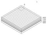
도 1은 본 발명의 일 실시예에 따른 발광소자 패키지를 갖는 디스플레이 패널의 개략 사시도이다.
도 2는 도 1의 'A'부분을 확대하여 나타낸 평면도이다.
도 3은 도 2의 I-I'선을 따라 절개하여 본 측 단면도이다.
도 4a는 도 3의 'B'부분의 확대도이다.
도 4b는 도 4a의 디스플레이 패널의 비교예이다.
도 5는 본 발명의 일 실시예에 따른 디스플레이 패널의 측 단면도이다.
도 6 내지 도 16은 도 3의 디스플레이 패널의 주요 제조공정을 개략적으로 설명하기 위한 도면이다.
도 17 내지 도 20은 도 5의 디스플레이 패널의 주요 제조공정을 개략적으로 설명하기 위한 도면이다.FIG. 1 is a schematic perspective view of a display panel having a light-emitting device package according to one embodiment of the present invention.
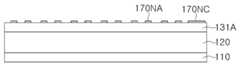
Figure 2 is a plan view showing an enlarged view of part 'A' of Figure 1.
Figure 3 is a cross-sectional side view taken along line I-I' of Figure 2.
Figure 4a is an enlarged view of part 'B' of Figure 3.
Fig. 4b is a comparative example of the display panel of Fig. 4a.
FIG. 5 is a cross-sectional side view of a display panel according to one embodiment of the present invention.
Figures 6 to 16 are drawings for schematically explaining the main manufacturing process of the display panel of Figure 3.
Figures 17 to 20 are drawings for schematically explaining the main manufacturing process of the display panel of Figure 5.
이하, 첨부된 도면을 참조하여 본 발명의 다양한 실시예를 상세히 설명한다.Hereinafter, various embodiments of the present invention will be described in detail with reference to the attached drawings.
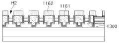
도 1은 본 발명의 일 실시예에 따른 발광소자 패키지를 갖는 디스플레이 패널의 개략 사시도이고, 도 2는 도 1의 'A'부분을 확대하여 나타낸 평면도이다. 도 3은 도 2의 I-I'선을 따라 절개하여 본 측 단면도이고, 도 4a는 도 3의 'B'부분의 확대도이다.
FIG. 1 is a schematic perspective view of a display panel having a light-emitting device package according to one embodiment of the present invention, and FIG. 2 is a plan view showing an enlarged portion 'A' of FIG. 1. FIG. 3 is a side cross-sectional view taken along line I-I' of FIG. 2, and FIG. 4A is an enlarged view of portion 'B' of FIG. 3.
도 1을 참조하면, 본 발명의 일 실시예에 의한 디스플레이 패널(1)은 발광소자 패키지로 이루어진 제1 기판 구조물(100)과, 제1 기판 구조물(100)의 하부에 배치되며 구동회로부를 포함하는 제2 기판 구조물(300)을 포함할 수 있다. 제1 기판 구조물(100)의 상면에는 보호층(400)이 배치될 수 있으며, 제1 기판 구조물(100)과 제2 기판 구조물(300)의 사이에는 본딩층(200)이 배치될 수 있다. 디스플레이 패널(1)은 사각형 형상이거나 다른 적합한 형상을 가질 수 있다. 디스플레이 패널(1)은 플렉시블(flexible)한 특성을 가질 수 있다. 따라서, 디스플레이 패널(1)의 상부면은 평면 이외에도 곡면의 프로파일을 가질 수 있다. 일 실시예의 디스플레이 패널(1)은 가상현실(virtual reality) 또는 증강현실(augmented reality)용 헤드셋(head set)에 사용되는 초소형 및 초고해상도의 디스플레이 패널일 수 있다.Referring to FIG. 1, a display panel (1) according to one embodiment of the present invention may include a first substrate structure (100) formed of a light emitting element package, and a second substrate structure (300) disposed below the first substrate structure (100) and including a driving circuit unit. A protective layer (400) may be disposed on an upper surface of the first substrate structure (100), and a bonding layer (200) may be disposed between the first substrate structure (100) and the second substrate structure (300). The display panel (1) may have a rectangular shape or another suitable shape. The display panel (1) may have a flexible characteristic. Accordingly, the upper surface of the display panel (1) may have a curved profile in addition to a flat surface. The display panel (1) according to one embodiment may be an ultra-small and ultra-high-resolution display panel used in a headset for virtual reality or augmented reality.
도 2를 참조하면, 제1 기판 구조물(100)은 픽셀 영역(10)및 픽셀 영역(10)을 둘러싸는 몰딩 영역(20)을 포함할 수 있다. 픽셀 영역(10)에는 복수의 픽셀(P)이 행(column)과 열(row)을 이루어 배치될 수 있다. 본 실시예에 따른 복수의 픽셀(P)은 15×15인 사각형태의 어레이를 이루는 것으로 도시되어 있으나, 행과 열의 개수는 임의의 적절한 개수(예, 1024×768, 1920×1080, 3840×2160, 7680×4320)로 구현될 수 있으며, 사각형 이외의 다양한 형상으로 배열될 수 있다. 복수의 픽셀(P)은 서로 전기적으로 연결될 수 있다. 또한, 복수의 픽셀(P)은 별개로 제조되는 것이 아니라, 동일한 공정에서 전체가 한번에 제조될 수 있다.Referring to FIG. 2, the first substrate structure (100) may include a pixel region (10) and a molding region (20) surrounding the pixel region (10). In the pixel region (10), a plurality of pixels (P) may be arranged in rows and columns. The plurality of pixels (P) according to the present embodiment are illustrated as forming a 15×15 rectangular array, but the number of rows and columns may be implemented as any appropriate number (e.g., 1024×768, 1920×1080, 3840×2160, 7680×4320) and may be arranged in various shapes other than a rectangular shape. The plurality of pixels (P) may be electrically connected to each other. In addition, the plurality of pixels (P) may not be manufactured separately, but may be manufactured all at once in the same process.
일 실시예의 경우, 복수의 픽셀(P)은 8000PPI(pixel per inch) 이상의 밀도를 갖도록 배치될 수 있다. 복수의 픽셀(P)은 각각 약 3㎛ 이하의 폭을 가질 수 있다.In one embodiment, the plurality of pixels (P) may be arranged to have a density of 8000 PPI (pixels per inch) or more. The plurality of pixels (P) may each have a width of about 3 μm or less.
픽셀 영역(10)의 둘레에는 몰딩 영역(20)이 배치될 수 있다. 몰딩 영역(20)은 블랙 매트릭스(black matrix)를 포함할 수 있다. 예를 들어, 블랙 매트릭스는 제1 기판 구조물(100)의 둘레 영역에 배치되어 복수의 픽셀(P)이 배치되는 영역을 정의하는 가이드 라인으로서 역할을 할 수 있다. 블랙 매트릭스는 블랙(black) 색상에 한정되는 것은 아니며 제품의 용도 및 사용처 등에 따라 백색(white) 매트릭스 또는 녹색(green) 등 다른 색깔로도 사용할 수 있으며 필요에 따라서는 투명 재질의 매트릭스를 사용할 수도 있다. 몰딩 영역(20)에는 후술하는 공통 제1 전극(170N)의 패드부(170NC)가 배치될 수 있다.
A molding region (20) may be arranged around the perimeter of the pixel region (10). The molding region (20) may include a black matrix. For example, the black matrix may be arranged around the perimeter of the first substrate structure (100) to serve as a guide line defining an area where a plurality of pixels (P) are arranged. The black matrix is not limited to the color black, and may be used in other colors such as a white matrix or green depending on the purpose and use of the product, and a matrix of a transparent material may also be used if necessary. A pad portion (170NC) of a common first electrode (170N) described below may be arranged in the molding region (20).
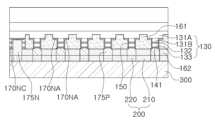
도 3 및 도 4a를 참조하면, 복수의 픽셀(P)은 각각 상하로 적층된 제1 기판 구조물(100)과 제2 기판 구조물(300)을 포함할 수 있다. 제1 기판 구조물(100)과 제2 기판 구조물(300)은 본딩층(200)에 의해 접합될 수 있다. 제1 기판 구조물(100)의 상부에는 보호층(400)이 접합될 수 있다. 제1 기판 구조물(100)과 제2 기판 구조물(300)은 서로 웨이퍼 레벨에서 퓨전 본딩(fusion bonding)과 같은 웨이퍼 접합방법에 의해 접합되어 일체가 될 수 있다.
Referring to FIGS. 3 and 4A, each of the plurality of pixels (P) may include a first substrate structure (100) and a second substrate structure (300) that are stacked vertically. The first substrate structure (100) and the second substrate structure (300) may be bonded by a bonding layer (200). A protective layer (400) may be bonded to an upper portion of the first substrate structure (100). The first substrate structure (100) and the second substrate structure (300) may be bonded to each other at the wafer level by a wafer bonding method such as fusion bonding to become one body.
복수의 픽셀(P)은 제1 및 제2 픽셀(P1, P2)을 포함하는 복수 개로 이루어질 수 있다. 이하에서는 설명의 편의를 위해, 제1 및 제2 픽셀(P1, P2)을 중심으로 설명한다. 제1 및 제2 픽셀(P1, P2)은 각각 복수의 서브 픽셀(SP1, SP2, SP3)을 포함할 수 있으며, 복수의 서브 픽셀(SP1, SP2, SP3)은 각각 제1 내지 제3 반도체 발광부(LED1, LED2, LED3) 중 하나를 포함할 수 있다. 일 실시예 경우, 복수의 서브 픽셀(SP1, SP2, SP3)은 각각 약 1.2㎛ 이하의 폭(WD)을 가질 수 있다
The plurality of pixels (P) may be composed of a plurality of first and second pixels (P1, P2). For convenience of explanation, the first and second pixels (P1, P2) will be described below. The first and second pixels (P1, P2) may each include a plurality of sub-pixels (SP1, SP2, SP3), and the plurality of sub-pixels (SP1, SP2, SP3) may each include one of the first to third semiconductor light-emitting units (LED1, LED2, LED3). In one embodiment, the plurality of sub-pixels (SP1, SP2, SP3) may each have a width (WD) of about 1.2 μm or less.
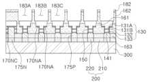
제1 기판 구조물(100)은 제1 내지 제3 반도체 발광부(LED1, LED2, LED3)를 포함하는 발광소자 패키지(LP1)를 포함할 수 있다. 발광소자 패키지(LP1)는 제1 내지 제3 반도체 발광부(LED1, LED2, LED3)에 각각 접속된 제1 및 제2 전극 패드(175N, 175P), 제1 내지 제3 반도체 발광부(LED1, LED2, LED3) 상에 각각 배치된 제1 내지 제3 파장변환부(190R, 190G, 190B), 반도체 발광부(LED1, LED2, LED3) 및 제1 내지 제3 파장변환부(190R, 190G, 190B)를 봉지하는 몰딩부(160)를 포함할 수 있다. 몰딩부(160)는 제1 몰딩부(161), 제2 몰딩부(161) 및 제3 몰딩부(163)을 포함할 수 있다.
The first substrate structure (100) may include a light-emitting device package (LP1) including first to third semiconductor light-emitting units (LED1, LED2, LED3). The light-emitting device package (LP1) may include first and second electrode pads (175N, 175P) respectively connected to the first to third semiconductor light-emitting units (LED1, LED2, LED3), first to third wavelength conversion units (190R, 190G, 190B) respectively arranged on the first to third semiconductor light-emitting units (LED1, LED2, LED3), and a molding unit (160) that encapsulates the semiconductor light-emitting units (LED1, LED2, LED3) and the first to third wavelength conversion units (190R, 190G, 190B). The molding part (160) may include a first molding part (161), a second molding part (161), and a third molding part (163).
제1 내지 제3 반도체 발광부(LED1, LED2, LED3)는 각각 제1 도전형 반도체층(131), 활성층(132) 및 제2 도전형 반도체층(133)과 같은 에피텍셜층들이 적층된 발광 구조물(130)을 포함할 수 있다. 이러한 에피택셜층들은 하나의 웨이퍼에서 동일한 공정에 의해 성장될 수 있다. 따라서, 제1 내지 제3 반도체 발광부(LED1, LED2, LED3)의 활성층(132)은 동일한 빛을 방출하도록 구성될 수 있다. 예를 들어, 활성층(132)은 청색광(예, 440㎚~460㎚)을 방출할 수 있다. 제1 내지 제3 반도체 발광부(LED1, LED2, LED3)는 동일한 구조를 질 수 있다.
The first to third semiconductor light-emitting units (LED1, LED2, LED3) may each include a light-emitting structure (130) in which epitaxial layers, such as a first conductive semiconductor layer (131), an active layer (132), and a second conductive semiconductor layer (133), are laminated. These epitaxial layers may be grown on a single wafer by the same process. Accordingly, the active layers (132) of the first to third semiconductor light-emitting units (LED1, LED2, LED3) may be configured to emit the same light. For example, the active layer (132) may emit blue light (e.g., 440 nm to 460 nm). The first to third semiconductor light-emitting units (LED1, LED2, LED3) may have the same structure.
제1 도전형 반도체층(131) 및 제2 도전형 반도체층(133)은 각각 n형 반도체층 및 p형 반도체층일 수 있다. 예를 들어, AlxInyGa(1-x-y)N(0≤x≤1, 0≤y≤1, 0≤x+y≤1)의 질화물 반도체일 수 있다. 활성층(132)은 양자우물층과 양자장벽층이 서로 교대로 적층된 다중 양자우물(MQW) 구조를 포함할 수 있다. 예를 들어, 활성층(132)은 InGaN/GaN, GaN/AlGaN와 같은 질화물계 MQW일 수 있으나, 이에 한정되지 않으며 GaAs/AlGaAs 또는 InGaP/GaP, GaP/AlGaP와 같은 다른 반도체일 수 있다. 이 중 제1 도전형 반도체층(131)은 단차진 측면을 가지도록 일부 영역만 식각될 수 있다.The first conductive semiconductor layer (131) and the second conductive semiconductor layer (133) may be an n-type semiconductor layer and a p-type semiconductor layer, respectively. For example, they may be a nitride semiconductor of Alx Iny Ga(1-xy) N (0≤x≤1, 0≤y≤1, 0≤x+y≤1). The active layer (132) may include a multiple quantum well (MQW) structure in which quantum well layers and quantum barrier layers are alternately stacked. For example, the active layer (132) may be a nitride-based MQW such as InGaN/GaN, GaN/AlGaN, but is not limited thereto and may be another semiconductor such as GaAs/AlGaAs or InGaP/GaP, GaP/AlGaP. Among these, only a portion of the first conductive semiconductor layer (131) may be etched so as to have a stepped side surface.
또한, 도 4a를 참조하면, 발광 구조물(130)은 파장변환부(190R)와 접하는 제1 면(S1)의 폭(W1)이 하부의 제2 면(S2)의 폭(W3)에 비해 넓게 형성될 수 있다. 또한, 발광 구조물(130)의 상면의 폭(W1)은 파장변환부(190R)의 폭(W2)보다 작게 형성되어, 파장변환부(190R)와 중첩되는 영역 내에 제한적으로 배치될 수 있다. 이러한 구조로 인해, 발광 구조물(130)의 활성층(132)에서 방출된 빛 중 상부의 파장변환부(190R)를 향하는 빛은 광경로 상에 별다른 장애물 없이 파장변환부(190R)를 통해 방출될 수 있다. 즉, 제1 도전형 반도체층(131)은 제1 상부 도전형 반도체층(131A)의 하부에 더 좁은 폭을 갖는 제1 하부 도전형 반도체층(131B)이 배치된 구조일 수 있다. 또한, 제1 상부 도전형 반도체층(131A)은 후술하는 제1 몰딩부(161) 상에 소정 두께(D)로 돌출되도록 배치될 수 있다.In addition, referring to FIG. 4a, the light emitting structure (130) may be formed so that the width (W1) of the first surface (S1) in contact with the wavelength conversion part (190R) is wider than the width (W3) of the second surface (S2) at the bottom. In addition, the width (W1) of the upper surface of the light emitting structure (130) may be formed smaller than the width (W2) of the wavelength conversion part (190R), so that the light may be placed within a limited area overlapping with the wavelength conversion part (190R). Due to this structure, light emitted from the active layer (132) of the light emitting structure (130) toward the wavelength conversion part (190R) at the top may be emitted through the wavelength conversion part (190R) without any particular obstacles in the optical path. That is, the first conductive semiconductor layer (131) may have a structure in which a first lower conductive semiconductor layer (131B) having a narrower width is arranged below the first upper conductive semiconductor layer (131A). In addition, the first upper conductive semiconductor layer (131A) may be arranged to protrude to a predetermined thickness (D) on the first molding portion (161) described below.
발광 구조물(130)의 측면에는 절연층(150)이 배치되어, 복수의 발광 구조물(130) 사이의 광학적 간섭을 차단하고, 서로 전기적으로 분리시킬 수 있다. 또한, 절연층(150)은 후술하는 공통 제1 전극(170N)과 맞닿도록 배치될 수 있다. 절연층(150)은 전기적으로 절연성을 갖는 물질로 이루어질 수 있다. 예를 들어, 절연층(150)은 실리콘 산화물, 실리콘 산질화물, 실리콘 질화물일 수 있다. 또한, 절연층(150)은 추가적으로 광흡수율이 낮거나 반사성을 갖는 물질 또는 반사성 구조를 포함할 수 있다.
An insulating layer (150) is arranged on the side of the light-emitting structure (130) to block optical interference between a plurality of light-emitting structures (130) and electrically isolate them from each other. In addition, the insulating layer (150) may be arranged to be in contact with a common first electrode (170N) described later. The insulating layer (150) may be made of an electrically insulating material. For example, the insulating layer (150) may be silicon oxide, silicon oxynitride, or silicon nitride. In addition, the insulating layer (150) may additionally include a material or a reflective structure having low light absorption or reflectivity.
제1 도전형 반도체층(131)과 제2 도전형 반도체층(133) 상에는 각각 공통 제1 전극(170N) 및 제2 전극(141)이 배치될 수 있다. 공통 제1 전극(170N)은 복수의 발광 구조물(130)에 포함된 각각의 제1 도전형 반도체층(131)을 서로 연결할 수 있다. 각각의 제1 내지 제3 반도체 발광부(LED1, LED2, LED3)에 전원을 인가하기 위한 제1 및 제2 전극 패드(175N, 175P)를 포함할 수 있다. 제1 및 제2 전극 패드(175N, 1750P)는 각각 공통 제1 전극 및 제2 전극(170N, 141)과 접속될 수 있다.
A common first electrode (170N) and a second electrode (141) may be arranged on the first conductive semiconductor layer (131) and the second conductive semiconductor layer (133), respectively. The common first electrode (170N) may connect each of the first conductive semiconductor layers (131) included in the plurality of light-emitting structures (130) to each other. First and second electrode pads (175N, 175P) for applying power to each of the first to third semiconductor light-emitting units (LED1, LED2, LED3) may be included. The first and second electrode pads (175N, 1750P) may be connected to the common first electrode and the second electrode (170N, 141), respectively.
도 2 및 도 4a를 참조하면, 공통 제1 전극(170N)은 개별 전극부(170NA), 패드부(170NC) 및 연결부(170NB)를 포함할 수 있다. 개별 전극부(170NA)는 복수의 발광 구조물(130)과 중첩하는 영역에 배치되며 각각의 제1 도전형 반도체층(131)에 접속될 수 있다. 개별 전극부(170NA)는 각각 발광 구조물(130)의 제1 상부 도전형 반도체층(131A)의 표면에 제2 하부 도전형 반도체층(131B)의 둘레를 둘러싸도록 링(ring) 형상으로 배치될 수 있다. 이와 같은 구조를 통해, 개별 전극부(170NA)에서 발광 구조물(130)에 공급되는 전류의 분배가 빠르게 이루어질 수 있다.Referring to FIG. 2 and FIG. 4A, the common first electrode (170N) may include an individual electrode portion (170NA), a pad portion (170NC), and a connection portion (170NB). The individual electrode portion (170NA) may be arranged in an area overlapping a plurality of light-emitting structures (130) and may be connected to each of the first conductive semiconductor layers (131). The individual electrode portions (170NA) may be arranged in a ring shape to surround the perimeter of the second lower conductive semiconductor layer (131B) on the surface of the first upper conductive semiconductor layer (131A) of the light-emitting structure (130). Through this structure, the distribution of current supplied from the individual electrode portion (170NA) to the light-emitting structure (130) may be performed quickly.
패드부(170NC)는 복수의 발광 구조물(130)과 중첩하지 않도록 디스플레이 패널의 몰딩 영역(20)에 배치될 수 있다. 예를 들어, 패드부(170NC)는 디스플레이 패널(1)의 각 모서리에 배치될 수 있다. 연결부(170NB)는 복수의 개별 전극부(170NA) 사이를 연결할 수 있으며, 개별 전극부(170NA)와 패드부(170NC)를 연결할 수 있다.The pad portion (170NC) may be placed in the molding area (20) of the display panel so as not to overlap with a plurality of light-emitting structures (130). For example, the pad portion (170NC) may be placed at each corner of the display panel (1). The connecting portion (170NB) may connect between a plurality of individual electrode portions (170NA) and may connect the individual electrode portions (170NA) and the pad portion (170NC).
공통 제1 전극(170N)은 발광 구조물(130)의 제1 면(S1) 및 제2 면(S2)과 평행한 면에 배치되어, 복수의 제1 도전형 반도체층(131)을 측면으로 서로 전기적으로 연결할 수 있다. 따라서, 공통 제1 전극(170N)과 제2 전극(141)에 전원을 인가하기 위해 배치된 제1 전극 패드(175N)와 제2 전극 패드(175P)는 서로 다른 영역에 배치되도록 구성될 수 있다. 즉, 제1 전극 패드(175N)는 디스플레이 패널(1)의 몰딩 영역(20)에 배치된 패드부(170NC)와 접하도록 배치될 수 있으며, 제2 전극 패드(175P)는 복수의 발광 구조물(130)의 하부에 각각 배치될 수 있다. 공통 제1 전극(170N)은 텅스텐(W) 및 텅스텐 실리사이드(WS)와 같은 녹는 점이 높은 물질로 이루어질 수 있다. 공통 제1 전극(170N)은, 제조 공정 중 제1 도전형 반도체층(131)의 내부에 매립된 후, 제1 도전형 반도체층(131)의 일부 영역을 식각하는 과정을 거쳐 노출되는데, 반도체 적층체의 컨택 성능 향상을 위해 고온의 열처리 과정을 거치게 된다. 텅스텐(W) 및 텅스텐 실리사이드(WS)와 같은 높은 녹는 점을 가지는 물질은 이 과정에서 용해 되지 않으나, 녹는 점이 상대적으로 낮은 물질의 경우, 고온의 열처리 과정에서 손상되어 전극으로서의 기능을 상실할 수 있다.
The common first electrode (170N) is arranged on a surface parallel to the first surface (S1) and the second surface (S2) of the light-emitting structure (130), so as to electrically connect the plurality of first conductive semiconductor layers (131) laterally. Accordingly, the first electrode pad (175N) and the second electrode pad (175P) arranged to apply power to the common first electrode (170N) and the second electrode (141) may be configured to be arranged in different regions. That is, the first electrode pad (175N) may be arranged to be in contact with the pad portion (170NC) arranged in the molding region (20) of the display panel (1), and the second electrode pad (175P) may be arranged on the lower portions of the plurality of light-emitting structures (130), respectively. The common first electrode (170N) may be made of a material having a high melting point, such as tungsten (W) and tungsten silicide (WS). The common first electrode (170N) is embedded in the interior of the first conductive semiconductor layer (131) during the manufacturing process, and then exposed through a process of etching a portion of the first conductive semiconductor layer (131), and is subjected to a high-temperature heat treatment process to improve the contact performance of the semiconductor laminate. Materials with high melting points, such as tungsten (W) and tungsten silicide (WS), do not melt during this process, but materials with relatively low melting points may be damaged during the high-temperature heat treatment process and lose their function as an electrode.
몰딩부(160)는, 제1 내지 제3 반도체 발광부(LED1, LED2, LED3)의 측면을 덮는 제1 몰딩부(161), 제1 내지 제3 파장변환부(190R, 190G, 190B)를 서로 분리하도록 제1 내지 제3 반도체 발광부(LED1, LED2, LED3) 사이로 돌출된 격벽 구조를 갖는 제2 몰딩부(162) 및, 제1 몰딩부(161)을 덮으며 제1 및 제2 전극 패드(175N, 175P)가 노출되는 제3 몰딩부(163)를 포함할 수 있다.
The molding part (160) may include a first molding part (161) that covers the side surfaces of the first to third semiconductor light-emitting parts (LED1, LED2, LED3), a second molding part (162) that has a partition structure that protrudes between the first to third semiconductor light-emitting parts (LED1, LED2, LED3) to separate the first to third wavelength conversion parts (190R, 190G, 190B) from each other, and a third molding part (163) that covers the first molding part (161) and exposes the first and second electrode pads (175N, 175P).
몰딩부(160)는 제1 기판 구조물(100)이 플렉시블(flexible)한 특성을 갖도록 낮은 모듈러스(modulus)를 갖는 물질로 이루어질 수 있다. 특히, 제1 몰딩부(161)는 발광 구조물(130) 보다 낮은 모듈러스를 가지며 높은 인장특성을 갖는 물질로 이루어 질 수 있다. 예를 들어, 제1 몰딩부(161)는 폴리이미드(polyimide, PI), 폴리사이클로핵실렌디메틸렌 테레프탈레이트(polycyclohexylenedimethylene terephthalate, PCT) 및 에폭시 몰딩 컴파운드(epoxy molding compound, EMC) 중 하나를 포함하는 물질로 이루어질 수 있다. 또한, 제1 몰딩부(161)는 빛을 반사시키기 위한 광반사성 입자를 포함할 수 있다. 광반사성 입자로는 이산화 티타늄(TiO2) 또는 산화 알루미늄(Al2O3)이 사용될 수 있으나, 이에 한정되는 것은 아니다.The molding portion (160) may be formed of a material having a low modulus so that the first substrate structure (100) has flexible characteristics. In particular, the first molding portion (161) may be formed of a material having a lower modulus than the light-emitting structure (130) and a high tensile characteristic. For example, the first molding portion (161) may be formed of a material including one of polyimide (PI), polycyclohexylenedimethylene terephthalate (PCT), and epoxy molding compound (EMC). In addition, the first molding portion (161) may include light-reflective particles for reflecting light. As the light-reflective particles, titanium dioxide (TiO2 ) or aluminum oxide (Al2 O3 ) may be used, but is not limited thereto.
일 실시예는, 제1 몰딩부(161)를, 반사율이 높은 폴리사이클로핵실렌디메틸렌 테레프탈레이트 (polycyclohexylenedimethylene terephthalate, PCT) 및 백색 에폭시 몰딩 컴파운드(white epoxy molding compound, white EMC)로 형성할 수 있으며, 이 경우, 별도의 반사층이 없이도 제1 몰딩부(161) 만으로도 충분한 광반사 효과를 기대할 수 있다. 다만, 이러한 물질은 녹는점이 230℃ 이하 이므로, 350℃ 이상의 온도에서 이루어지는 본딩 공정에서 녹을 수 있다. 이 경우 제1 몰딩부(161)는 외형이 변형되어 몰딩으로서의 기능을 상실할 수 있다. 따라서, 제1 몰딩부(161)의 하부에는, 본딩 공정에서 녹지 않는 정도의 녹는점을 가진 폴리이미드(polyimide, PI)와 같은 물질층인 제3 몰딩부(163)를 형성하여, 제1 몰딩부(161)가 본딩 공정에서 녹게되더라도, 외형을 유지하여 몰딩으로서의 기능을 유지하게 할 수 있다.
In one embodiment, the first molding part (161) may be formed of highly reflective polycyclohexylenedimethylene terephthalate (PCT) and white epoxy molding compound (white EMC). In this case, a sufficient light reflection effect may be expected with only the first molding part (161) without a separate reflective layer. However, since this material has a melting point of 230° C. or lower, it may melt during a bonding process performed at a temperature of 350° C. or higher. In this case, the first molding part (161) may be deformed in appearance and lose its function as a molding. Accordingly, a third molding part (163), which is a material layer such as polyimide (PI) that has a melting point that does not melt during the bonding process, is formed at the lower portion of the first molding part (161), so that even if the first molding part (161) melts during the bonding process, the outer shape can be maintained and the function as a molding can be maintained.
제2 몰딩부(162)는 제1 내지 제3 파장변환부(190R, 190G, 190B)의 측면들 둘러싸서 서로 분리하는 격벽 구조로 형성되어, 제1 내지 제3 반도체 발광부(LED1, LED2, LED3)의 상부에 각각 제1 내지 제3 파장변환부(190R, 190G, 190B)가 서로 분리되어 배치될 수 있다. 따라서, 제1 내지 제3 반도체 발광부(LED1, LED2, LED3)에서 각각 방출된 빛은 서로 광간섭을 받지 않고, 제1 내지 제3 반도체 발광부(LED1, LED2, LED3)의 상부에 배치된 제1 내지 제3 파장변환부(190R, 190G, 190B)를 통해 방출될 수 있다. 제2 몰딩부(162)는 블랙 매트릭스(black matrix)를 포함하는 물질로 이루어질 수 있다. 제2 몰딩부(161)의 상면에는 텅스텐(W) 및 텅스텐 실리사이드(WS)와 같은 금속 물질로 이루어진 반사층(182)이 배치될 수 있다.
The second molding portion (162) is formed as a partition structure that surrounds the side surfaces of the first to third wavelength conversion portions (190R, 190G, 190B) and separates them from each other, so that the first to third wavelength conversion portions (190R, 190G, 190B) can be separated from each other and arranged on top of the first to third semiconductor light-emitting portions (LED1, LED2, LED3), respectively. Therefore, the light emitted from each of the first to third semiconductor light-emitting portions (LED1, LED2, LED3) can be emitted through the first to third wavelength conversion portions (190R, 190G, 190B) arranged on top of the first to third semiconductor light-emitting portions (LED1, LED2, LED3) without being subject to optical interference. The second molding portion (162) can be made of a material including a black matrix. A reflective layer (182) made of a metal material such as tungsten (W) and tungsten silicide (WS) may be placed on the upper surface of the second molding portion (161).
제1 내지 제3 파장변환부(190R, 190G, 190B)는 각각, 양자점(Quantum Dot, QD)과 같은 파장변환물질이 액상의 바인더 수지에 분산된 상태로, 몰딩부(160)의 격벽 구조 내에 충전되어 경화된 것 일 수 있다. 일 실시예의 경우, 제1 및 제2 파장변환부(190R, 190G)에는 각각 청색광을 적색광 및 녹색광으로 파장변환할 수 있는 양자점이 포함될 수 있으며, 제3 파장변환부(190B)는 별도의 양자점 없이 바인더 수지만 포함될 수 있다.The first to third wavelength conversion units (190R, 190G, 190B) may each be formed by filling and curing a partition structure of a molding unit (160) in which a wavelength conversion material, such as a quantum dot (QD), is dispersed in a liquid binder resin. In one embodiment, the first and second wavelength conversion units (190R, 190G) may each include a quantum dot capable of converting blue light into red light and green light, and the third wavelength conversion unit (190B) may include only a binder resin without a separate quantum dot.
구체적으로, 제1 및 제2 파장변환부(190R, 190G)는 각각 적색 양자점 및 녹색 양자점이 바인더 수지에 분산된 액상의 감광성 수지 조성물을 격벽 구조 내에 충전한 후, 경화하여 형성할 수 있다. 바인더 수지는 아크릴계 폴리머를 포함하는 물질로 이루어질 수 있다.Specifically, the first and second wavelength conversion units (190R, 190G) can be formed by filling a liquid photosensitive resin composition in which red quantum dots and green quantum dots are dispersed in a binder resin into a partition structure and then curing it. The binder resin can be made of a material including an acrylic polymer.
제1 내지 제3 파장변환부(190R, 190G, 190B)의 상부에는 제1 내지 제3 파장변환부(190R, 190G, 190B)의 열화를 방지하는 보호층(400)이 배치될 수 있다.
A protective layer (400) may be placed on the upper portion of the first to third wavelength conversion units (190R, 190G, 190B) to prevent deterioration of the first to third wavelength conversion units (190R, 190G, 190B).
제1 기판 구조물(100)의 하부에는 제2 기판 구조물(300)과 접합하기 위한 본딩층(200)이 배치될 수 있다. 본딩층(200)은 절연 본딩층(210) 및 도전 본딩층(220)을 포함할 수 있으며, 절연 본딩층(210)은 제1 기판 구조물(100)과 제2 기판 구조물(300)을 접합시킬 수 있다. 절연 본딩층(210)은 제1 기판 구조물(100)의 몰딩부(160)와 동일한 조성의 물질로 이루어질 수 있다. 도전 본딩층(220)은 제1 기판 구조물(300)의 제1 및 제2 전극 패드(175N, 175P)를 제2 기판 구조물(300)의 전극들과 접합하기 위한 것으로, 제1 및 제2 전극 패드(175N, 175P)와 동일한 조성의 도전성 물질로 이루어질 수 있다. 따라서, 제1 기판 구조물(100)과 제2 기판 구조물(300)은 본딩층(200)을 통해 서로 접합되어 일체로 될 수 있다.
A bonding layer (200) for bonding to a second substrate structure (300) may be arranged on a lower portion of the first substrate structure (100). The bonding layer (200) may include an insulating bonding layer (210) and a conductive bonding layer (220), and the insulating bonding layer (210) may bond the first substrate structure (100) and the second substrate structure (300). The insulating bonding layer (210) may be made of a material having the same composition as the molding portion (160) of the first substrate structure (100). The conductive bonding layer (220) may be made of a conductive material having the same composition as the first and second electrode pads (175N, 175P) of the first substrate structure (300) to the electrodes of the second substrate structure (300). Therefore, the first substrate structure (100) and the second substrate structure (300) can be joined to each other through the bonding layer (200) to become one body.
제2 기판 구조물(300)은 제1 기판 구조물(100)의 발광소자 패키지(LP1)를 제어하기 위한 복수의 TFT 셀을 포함하는 구동 회로(driving circuit)를 포함할 수 있다. 복수의 TFT 셀은 복수의 픽셀(P)의 구동을 제어하기 위한 TFT 회로(TFT circuitry)를 구성할 수 있다. 복수의 TFT 셀은 본딩층(200의 도전 본딩층(220)을 통해 각각 제1 내지 제3 반도체 발광부(LED1, LED2, LED3)에 대응되도록 접속될 수 있다. 복수의 TFT 셀은 반도체 기판에 불순물을 주입하여 형성된 반도체층을 포함할 수 있다. 예를 들어, 복수의 TFT 셀을 구성하는 반도체층은 폴리실리콘과 실리콘계 반도체, 인듐 갈륨 산화아연과 같은 반도체 산화물 또는 실리콘 저마늄과 같은 화합물 반도체를 포함할 수 있다
The second substrate structure (300) may include a driving circuit including a plurality of TFT cells for controlling the light-emitting device package (LP1) of the first substrate structure (100). The plurality of TFT cells may constitute a TFT circuitry for controlling the driving of a plurality of pixels (P). The plurality of TFT cells may be connected to correspond to the first to third semiconductor light-emitting units (LED1, LED2, LED3) through the conductive bonding layer (220) of the bonding layer (200). The plurality of TFT cells may include a semiconductor layer formed by injecting an impurity into a semiconductor substrate. For example, the semiconductor layer constituting the plurality of TFT cells may include polysilicon and a silicon-based semiconductor, a semiconductor oxide such as indium gallium zinc oxide, or a compound semiconductor such as silicon germanium.
일 실시예의 디스플레이 패널(1)은 실리콘 기판을 이용한 격벽 구조를 사용한 경우에 비해, 개구율이 우수한 장점이 있다. 도 4a 및 도 4b를 참조하여 이에 대하여 설명한다. 도 4b는 실리콘 기판으로 이루어진 격벽구조(2180)를 채용한 사용한 비교예를 도시한 것이다.The display panel (1) of one embodiment has an advantage of an excellent aperture ratio compared to a case where a partition structure using a silicon substrate is used. This will be described with reference to FIGS. 4a and 4b. FIG. 4b illustrates a comparative example in which a partition structure (2180) made of a silicon substrate is employed.
도 4b를 참조하면, 비교예의 경우, 픽셀의 화소 밀도가 커짐에 따라, 격벽 구조(2180)의 높이(L)와 광 방출창(LW)의 폭(W5)의 비율이 점점 커져 개구율(aperture ratio)이 점점 낮아지는 문제가 발생한다. 화소밀도가 증가하여, 픽셀이 소형화되더라도, 격벽 구조(2180)의 구조적 강성을 유지하기 위해 격벽 구조(2180)의 두께(W4)는 소정의 값 이하로 얇아질 수 없다. 즉, 화소밀도가 증가하여, 픽셀(P)의 크기가 작아질 수록, 격벽 구조(2180)에 형성된 광 방출창(LW)이 상하로 길고 좁은 형태가 되어 파장변환부(2190)의 형상도 좁고 길게 형성되게 된다. 따라서, 활성층(2132)에서 방출된 빛(L2)이 긴 발광경로를 따라 진행하는 동안 휘도가 더 낮아지는 문제가 발생한다.Referring to FIG. 4b, in the case of the comparative example, as the pixel density of the pixel increases, the ratio of the height (L) of the partition structure (2180) to the width (W5) of the light emission window (LW) gradually increases, resulting in a problem that the aperture ratio gradually decreases. Even if the pixel density increases and the pixel becomes smaller, the thickness (W4) of the partition structure (2180) cannot be thinned below a predetermined value in order to maintain the structural rigidity of the partition structure (2180). That is, as the pixel density increases and the size of the pixel (P) becomes smaller, the light emission window (LW) formed in the partition structure (2180) becomes longer and narrower vertically, resulting in the shape of the wavelength conversion unit (2190) also becoming narrower and longer. Therefore, a problem occurs in which the luminance decreases further while the light (L2) emitted from the active layer (2132) travels along a long light emission path.
또한, 광 방출창(LW)의 폭(W5)이 감소함에 따라, 제조공정에서의 공차에 의해 격벽 구조(2180)와 반도체 적층체(2130)가 서로 중첩되는 영역(A1)의 비율이 증가하는데, 격벽 구조(2180)와 반도체 적층체(2130)가 서로 중첩되는 영역(A1)에서는 빛(L3)이 격벽 구조(2180)에 흡수되거나 하부로 반사되어 광 방출창(LW)을 통해 방출되지 못하므로, 격벽 구조(2180)와 반도체 적층체(2130)가 서로 중첩되는 영역(A1)의 비율이 증가하면 디스플레이 패널의 전체적으로 휘도가 낮아지는 문제가 발생한다.In addition, as the width (W5) of the light emission window (LW) decreases, the ratio of the area (A1) where the barrier rib structure (2180) and the semiconductor laminate (2130) overlap each other increases due to tolerance in the manufacturing process. In the area (A1) where the barrier rib structure (2180) and the semiconductor laminate (2130) overlap each other, light (L3) is absorbed by the barrier rib structure (2180) or reflected downward and is not emitted through the light emission window (LW). Therefore, when the ratio of the area (A1) where the barrier rib structure (2180) and the semiconductor laminate (2130) overlap each other increases, a problem occurs in which the overall brightness of the display panel decreases.
일 실시예의 경우, 실리콘 기판을 이용한 격벽 구조를 반사율이 높은 물질이 포함된 몰딩부로 대체하여, 실리콘 격벽 구조에 비해 월등하게 얇은 두께의 파장변환부를 형성하는 것이 가능하다. 따라서, 좁고 긴 파장변환부를 통과하는 과정에서 휘도가 낮아지는 문제가 해소될 수 있다.In one embodiment, by replacing the barrier structure using a silicon substrate with a molding part containing a highly reflective material, it is possible to form a wavelength conversion part with a thickness that is much thinner than that of a silicon barrier structure. Accordingly, the problem of brightness being reduced in the process of passing through a narrow and long wavelength conversion part can be resolved.
또한, 격벽 구조가 얇아져, 파장변환부의 면적을 반도체 적층체(2130)에 비해 넓게 형성할 수 있으므로, 활성층(2132)에서 방출된 빛이 격벽 구조에 의해 가로 막히게 되는 문제점을 근본적으로 해결할 수 있다.
In addition, since the barrier rib structure becomes thinner, the area of the wavelength conversion section can be formed wider than that of the semiconductor laminate (2130), so that the problem of light emitted from the active layer (2132) being blocked by the barrier rib structure can be fundamentally solved.
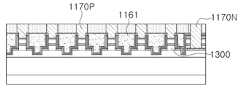
도 5는 본 발명의 일 실시예에 의한 발광소자 패키지(LP2)를 갖는 디스플레이 패널(2)의 단면도이다. 도 6의 디스플레이 패널(2)은 앞서 설명한 실시예의 디스플레이 패널(1)과 비교할 때, 제1 몰딩부(1161)가 PI로 형성되며, 반사율이 PCT나 EMC에 비해 상대적으로 낮은 PI의 특성 상, 반사율을 향상시키기 위한 반사층(1200)이 제1 내지 제3 반도체 발광부(LED4, LED5, LED6)의 측면에 형성된 차이점이 있다. 또한, 반사층(1200)과 제1 내지 제3 반도체 발광부(LED4, LED5, LED6)의 사이에 절연층(1100)이 배치되어 반사층(1200)과 제1 내지 제3 반도체 발광부(LED4, LED5, LED6) 사이를 절연할 수 있다. 그 외에는, 앞서 설명한 실시예와 유사하므로 중복되는 설명은 생략한다.
FIG. 5 is a cross-sectional view of a display panel (2) having a light-emitting device package (LP2) according to one embodiment of the present invention. The display panel (2) of FIG. 6, compared to the display panel (1) of the embodiment described above, has a difference in that a first molding portion (1161) is formed of PI, and a reflective layer (1200) for improving reflectivity is formed on the side surface of the first to third semiconductor light-emitting units (LED4, LED5, LED6) due to the characteristic of PI having a relatively low reflectivity compared to PCT or EMC. In addition, an insulating layer (1100) is disposed between the reflective layer (1200) and the first to third semiconductor light-emitting units (LED4, LED5, LED6) to insulate the reflective layer (1200) and the first to third semiconductor light-emitting units (LED4, LED5, LED6). Other than that, since it is similar to the embodiment described above, a redundant description will be omitted.
이하에서는, 일 실시예에 의한 디스플레이 패널의 제조공정에 대해 설명한다. 도 6 내지 도 16은 도 3의 디스플레이 패널의 주요 제조공정을 개략적으로 설명하기 위한 도면이다.
Below, a manufacturing process of a display panel according to one embodiment is described. FIGS. 6 to 16 are drawings for schematically explaining the main manufacturing process of the display panel of FIG. 3.
먼저, 도 6을 참조하면, 성장용 기판(110) 상에 버퍼층(120)을 형성하고, 버퍼층(120) 상에 제1 상부 도전형 반도체층(131A)을 형성할 수 있다. 제1 상부 도전형 반도체층(131A)상면에는 공통 제1 전극(170N)을 형성하기 위한 전극 패턴이 도 7과 같이 형성될 수 있으며, 제1 상부 도전형 반도체층(131A)의 모서리에는 공통 제1 전극(170N)의 패드부(170NC)가 배치될 수 있으며, 후속 공정에서 복수의 발광 구조물이 형성될 영역에는 각각 개별 전극부(170NA)가 배치될 수 있다. 또한, 패드부(170NC)와 개별 전극부(170NA)는 연결부(170NB)로 연결되어, 패드부(170NC)와 개별 전극부(170NA)는 전기적으로 연결될 수 있다. 공통 제1 전극(170N)으로 고온의 반도체 열처리 과정에서 녹지 않을 정도로 높은 녹는점을 갖는 텅스텐(W) 및 텅스텐 실리사이드(WS)가 사용될 수 있다.
First, referring to FIG. 6, a buffer layer (120) may be formed on a growth substrate (110), and a first upper conductive semiconductor layer (131A) may be formed on the buffer layer (120). An electrode pattern for forming a common first electrode (170N) may be formed on an upper surface of the first upper conductive semiconductor layer (131A), as shown in FIG. 7, and a pad portion (170NC) of the common first electrode (170N) may be arranged at a corner of the first upper conductive semiconductor layer (131A), and individual electrode portions (170NA) may be arranged in an area where a plurality of light-emitting structures are to be formed in a subsequent process. In addition, the pad portion (170NC) and the individual electrode portion (170NA) may be connected by a connection portion (170NB), so that the pad portion (170NC) and the individual electrode portion (170NA) may be electrically connected. Tungsten (W) and tungsten silicide (WS), which have a melting point high enough not to melt during a high-temperature semiconductor heat treatment process, can be used as a common first electrode (170N).
도 8을 참조하면, 제1 상부 도전형 반도체층(131A) 상에는 공통 제1 전극(170N)을 덮도록 제1 하부 도전형 반도체층(131B)이 형성될 수 있다. 제1 상부 도전형 반도체층(131A)과 제1 하부 도전형 반도체층(131B)은 동일한 조성의 반도체층으로 형성되어, 제1 도전형 반도체층(131)으로 일체화될 수 있다. 따라서, 공통 제1 전극(170N)은 제1 도전형 반도체층(131)에 매립될 수 있다. 계속하여, 제1 도전형 반도체층(131) 상에는 활성층(132)과 제2 도전형 반도체층(133)이 형성될 수 있다.
Referring to FIG. 8, a first lower conductive semiconductor layer (131B) may be formed on a first upper conductive semiconductor layer (131A) to cover a common first electrode (170N). The first upper conductive semiconductor layer (131A) and the first lower conductive semiconductor layer (131B) may be formed of semiconductor layers having the same composition and may be integrated into the first conductive semiconductor layer (131). Accordingly, the common first electrode (170N) may be embedded in the first conductive semiconductor layer (131). Subsequently, an active layer (132) and a second conductive semiconductor layer (133) may be formed on the first conductive semiconductor layer (131).
도 9를 참조하면, 제2 도전형 반도체층(133) 상에는 제2 전극(141)이 형성될 수 있으며, 제2 전극(141) 상에는 하드 마스크층(142)이 형성될 수 있다. 하드 마스크층(142)은 후속 공정에서 제2 전극(141)이 손상되는 것을 방지할 수 있다.
Referring to FIG. 9, a second electrode (141) may be formed on a second challenge type semiconductor layer (133), and a hard mask layer (142) may be formed on the second electrode (141). The hard mask layer (142) may prevent the second electrode (141) from being damaged in a subsequent process.
도 10을 참조하면, 공통 제1 전극(170N)을 식각 마스크로 하여, 공통 제1 전극(170N)이 노출될 때까지 식각을 진행할 수 있다. 이를 통해, 발광 구조물(130)의 일부영역(E)을 식각하여 메사영역(M)을 형성할 수 있다. 도 11을 참조하면, 발광 구조물(130)의 측면에는 절연층(150)이 형성될 수 있다.
Referring to Fig. 10, etching can be performed using the common first electrode (170N) as an etching mask until the common first electrode (170N) is exposed. Through this, a part of the region (E) of the light-emitting structure (130) can be etched to form a mesa region (M). Referring to Fig. 11, an insulating layer (150) can be formed on a side surface of the light-emitting structure (130).
도 12를 참조하면, 발광 구조물(130)을 덮도록 제1 몰딩부(161)를 형성하고 제1 몰딩부(161) 상에 제2 몰딩부(162)를 형성할 수 있다. 도 13을 참조하면, 제2 몰딩부(162) 중 일 영역을 식각하고 도전성 물질을 도금하여 공통 제1 전극(170N) 및 제2 전극(141)과 접하는 제1 전극 패드(175N) 및 제2 전극 패드(175P)를 형성할 수 있다.
Referring to FIG. 12, a first molding part (161) may be formed to cover a light-emitting structure (130), and a second molding part (162) may be formed on the first molding part (161). Referring to FIG. 13, a region of the second molding part (162) may be etched and a conductive material may be plated to form a first electrode pad (175N) and a second electrode pad (175P) that come into contact with the common first electrode (170N) and the second electrode (141).
도 14를 참조하면, 도 13의 제2 몰딩부(162)의 하부에 절연 본딩층(210) 및 도전 본딩층(220)을 포함하는 본딩층(200)을 개재하여 제2 기판 구조물(300)을 부착시킬 수 있다. 도 14는 도 13의 제1 전극 패드(175N) 및 제2 전극 패드(175P)가 하면에 배치되도록 뒤집은 것을 이해될 수 있다. 제2 기판 구조물(300)은 제1 내지 제3 반도체 발광부(LED1, LED2, LED3)를 제어하기 위한 복수의 TFT 셀을 포함하는 구동 회로(driving circuit)를 포함할 수 있다. 복수의 TFT 셀은 반도체 기판에 불순물을 주입하여 형성된 반도체층을 포함할 수 있다. 예를 들어, 복수의 TFT 셀을 구성하는 반도체층은 폴리실리콘과 실리콘계 반도체, 인듐 갈륨 산화아연과 같은 반도체 산화물 또는 실리콘 저마늄과 같은 화합물 반도체를 포함할 수 있다. 반도체 기판은 성장용 기판(110)을 분리하는 후속 공정에서 식각 선택성을 확보하기 위해, 성장용 기판(110)에 도핑된 농도보다 저 농도인 1016 /㎝-3 이하의 농도로 붕소가 도핑될 수 있다.
Referring to FIG. 14, a second substrate structure (300) may be attached to the lower portion of the second molding portion (162) of FIG. 13 by interposing a bonding layer (200) including an insulating bonding layer (210) and a conductive bonding layer (220). It can be understood that FIG. 14 is flipped so that the first electrode pad (175N) and the second electrode pad (175P) of FIG. 13 are disposed on the lower surface. The second substrate structure (300) may include a driving circuit including a plurality of TFT cells for controlling the first to third semiconductor light-emitting units (LED1, LED2, LED3). The plurality of TFT cells may include a semiconductor layer formed by injecting an impurity into a semiconductor substrate. For example, the semiconductor layer constituting the plurality of TFT cells may include polysilicon and a silicon-based semiconductor, a semiconductor oxide such as indium gallium zinc oxide, or a compound semiconductor such as silicon germanium. The semiconductor substrate may be doped with boron at a concentration of 1016 /cm-3 or less, which is lower than the doping concentration of the growth substrate (110), to secure etching selectivity in the subsequent process of separating the growth substrate (110).
도 15를 참조하면, 제1 내지 제3 반도체 발광부(LED1, LED2, LED3)에서 성장용 기판을 분리한 후 습식식각하여, 제1 내지 제3 반도체 발광부(LED1, LED2, LED3)를 서로 분리하는 아이솔레이션(ISO)공정을 수행할 수 있다.
Referring to FIG. 15, after separating the growth substrate from the first to third semiconductor light-emitting units (LED1, LED2, LED3), an isolation (ISO) process can be performed to separate the first to third semiconductor light-emitting units (LED1, LED2, LED3) from each other by wet etching.
도 16을 참조하면, 발광 구조물(130)의 상부에 블랙 매트릭스를 도포하여 제2 몰딩부(162)을 형성하고, 반사층(182)을 증착한 뒤, 일 영역을 식각하여, 후속공정에서 파장변환부(190)를 형성하기 위한 홈부(183A, 183B, 183C)를 형성할 수 있다. 계속하여, 양자점(Quantum Dot, QD)과 같은 파장변환물질을 액상의 바인더 수지에 분산된 상태로 홈부에 충전하여 파장변환부(190R, 190G, 190B)를 형성하고, 상부에 보호층(400)을 부착하면 도 3의 디스플레이 패널(1)을 제조할 수 있다.
Referring to FIG. 16, a black matrix is applied to the upper portion of a light-emitting structure (130) to form a second molding portion (162), a reflective layer (182) is deposited, and then an area is etched to form a recessed portion (183A, 183B, 183C) for forming a wavelength conversion portion (190) in a subsequent process. Subsequently, a wavelength conversion material such as a quantum dot (QD) is dispersed in a liquid binder resin and filled in the recessed portion to form a wavelength conversion portion (190R, 190G, 190B), and a protective layer (400) is attached to the upper portion, thereby manufacturing the display panel (1) of FIG. 3.
일 실시예에 의한 디스플레이 패널의 제조공정에 대해 설명한다. 도 17 내지 도 21는 도 5의 디스플레이 패널의 주요 제조공정을 개략적으로 설명하기 위한 도면이다. 도 17의 이전 공정은 앞서 설명한 실시예의 도 11까지의 공정과 동일하므로 생략한다. 도 17 내지 도 20은 도 5의 디스플레이 패널의 주요 제조공정을 개략적으로 설명하기 위한 도면이다. 또한, 일 실시예는 앞서 설명한 실시예와 비교할 때, 제1 몰딩부(1161)가 폴리이미드(polyimide, PI)로 형성되는 차이점이 있다.
Hereinafter, a manufacturing process of a display panel according to one embodiment will be described. FIGS. 17 to 21 are drawings for schematically explaining the main manufacturing process of the display panel of FIG. 5. The process before FIG. 17 is the same as the process up to FIG. 11 of the embodiment described above, and therefore is omitted. FIGS. 17 to 20 are drawings for schematically explaining the main manufacturing process of the display panel of FIG. 5. In addition, one embodiment has a difference in that the first molding part (1161) is formed of polyimide (PI) compared to the embodiment described above.
도 17을 참조하면, 발광 구조물(1130)의 측면에 반사층(1200)이 형성될 수 있다. 반사층(1200)은 알루미늄(Al)을 발광 구조물(1130)의 측면에 증착하여 형성할 수 있다. 반사층(1200)은 후속공정에서 제1 몰딩부(1161)가 PI로 형성되어, PCT나 EMC에 비해 반사율이 낮은 점을 보완하기 위한 것이다. 반사층(1200)과 발광 구조물(1130)의 사이의 절연을 위한 절연층(1100)이 개재될 수 있다.
Referring to FIG. 17, a reflective layer (1200) may be formed on a side surface of a light-emitting structure (1130). The reflective layer (1200) may be formed by depositing aluminum (Al) on the side surface of the light-emitting structure (1130). The reflective layer (1200) is formed of PI in a subsequent process to compensate for the lower reflectivity compared to PCT or EMC. An insulating layer (1100) may be interposed between the reflective layer (1200) and the light-emitting structure (1130).
도 18을 참조하면, 발광 구조물(1130)을 제1 몰딩부(1161)를 형성할 수 있다. 제1 몰딩부(1161)는 폴리사이클로핵실렌디메틸렌 테레프탈레이트 (polycyclohexylenedimethylene terephthalate, PCT) 및 에폭시 몰딩 컴파운드(epoxy molding compound, EMC) 중 적어도 하나를 포함하는 물질을 포함할 수 있다. 제1 몰딩부(1161)에 개구(H1)를 형성하여, 공통 제1 전극(1170N)과 제2 전극(1141)을 노출시킬 수 있다.
Referring to FIG. 18, a light-emitting structure (1130) may be formed to form a first molding portion (1161). The first molding portion (1161) may include a material including at least one of polycyclohexylenedimethylene terephthalate (PCT) and an epoxy molding compound (EMC). An opening (H1) may be formed in the first molding portion (1161) to expose a common first electrode (1170N) and a second electrode (1141).
도 19를 참조하면, 제1 몰딩부(1161) 상에 제2 몰딩부(1162)를 형성하고, 개구(H2, H3)를 형성하여, 패드부(1170NC)와 제2 전극(1141)을 노출시킬 할 수 있다. 제2 몰딩부(1162)는 PI 및 PBO(poly phenylene benzobisoxazole) 중 적어도 하나의 물질을 코팅하여 형성할 수 있다.
Referring to FIG. 19, a second molding part (1162) may be formed on a first molding part (1161), and openings (H2, H3) may be formed to expose a pad part (1170NC) and a second electrode (1141). The second molding part (1162) may be formed by coating at least one material among PI and PBO (poly phenylene benzobisoxazole).
도 20을 참조하면, 개구(H2, H3)에 각각 도전성 물질을 도금하여 공통 제1 전극(1170N)과 제2 전극(1141)과 접하는 제1 전극 패드(1175N) 및 제2 전극 패드(1175P)를 형성할 수 있다.
Referring to FIG. 20, a conductive material may be plated in each of the openings (H2, H3) to form a first electrode pad (1175N) and a second electrode pad (1175P) that come into contact with the common first electrode (1170N) and second electrode (1141).
이후, 앞서 설명한 실시예의 도 14 내지 도 20의 공정을 수행하면, 도 5의 디스플레이 패널(2)을 제조할 수 있다.
Thereafter, by performing the processes of FIGS. 14 to 20 of the above-described embodiment, the display panel (2) of FIG. 5 can be manufactured.
이상, 첨부된 도면을 참조하여 본 발명의 실시 예를 설명하였지만, 본 발명이 속하는 기술분야에서 통상의 지식을 가진 자는 본 발명이 그 기술적 사상이나 필수적인 특징을 변경하지 않고서 다른 구체적인 형태로 실시될 수 있다는 것을 이해할 수 있을 것이다. 그러므로 이상에서 기술한 실시 예에는 모든 면에서 예시적인 것이며 한정적이 아닌 것으로 이해해야만 한다.
Above, while the embodiments of the present invention have been described with reference to the attached drawings, those skilled in the art to which the present invention pertains will understand that the present invention can be implemented in other specific forms without changing the technical idea or essential features thereof. Therefore, it should be understood that the embodiments described above are exemplary in all respects and not restrictive.
100: 제1 기판 구조물
200: 본딩층
300: 제2 기판 구조물
400: 보호층100: First substrate structure
200: Bonding layer
300: Second substrate structure
400: Protective layer
Claims (10)
Translated fromKorean상기 복수의 발광 구조물의 각각의 제1 도전형 반도체층을 서로 연결하며 상기 제1 및 제2 면과 다른 레벨로 평행하게 연장되고, 텅스텐(W) 및 텅스텐 실리사이드(WS) 중 적어도 하나를 포함하는 물질로 이루어진 공통 제1 전극;
상기 복수의 발광 구조물의 상기 제2 면 상에 배치되며, 상기 복수의 발광 구조물의 각각의 제2 도전형 반도체층에 연결된 복수의 제2 전극;
상기 제1 면 상에 상기 복수의 발광 구조물 각각에 대응되도록 이격하여 배치된 복수의 파장변환부;
상기 복수의 발광 구조물의 측면을 덮으며, 상기 복수의 발광 구조물보다 낮은 모듈러스(modulus)를 갖는 물질로 이루어진 제1 몰딩부; 및
상기 제1 몰딩부 상에서, 상기 복수의 파장변환부의 측면을 덮으며, 상기 복수의 파장변환부를 서로 분리하는 격벽구조를 가지는 제2 몰딩부;를 포함하고,
상기 공통 제1 전극은,
상기 복수의 발광 구조물과 중첩하는 영역에 배치되며 각각의 제1 도전형 반도체층에 접속되는 복수의 개별 전극부;
상기 복수의 발광 구조물과 중첩하지 않는 영역에 배치되는 적어도 하나의 패드부; 및
상기 복수의 개별 전극부를 각각 연결하며, 상기 복수의 개별 전극부 중 적어도 하나와 상기 패드부를 연결하는 연결부;를 포함하고,
상기 복수의 개별 전극부는, 상기 제1 도전형 반도체층의 적어도 일 측면과 접하며, 상기 제1 도전형 반도체층의 적어도 일부의 둘레를 둘러싸도록 배치되는 발광소자 패키지.
A plurality of light-emitting structures, each having a first conductive semiconductor layer, an active layer, and a second conductive semiconductor layer, the light-emitting structures being spaced apart from each other and having a first surface provided by the first conductive semiconductor layer and a second surface provided by the second conductive semiconductor layer located in a direction opposite to the first surface;
A common first electrode connecting the first conductive semiconductor layers of each of the plurality of light-emitting structures to each other and extending parallel to the first and second surfaces at different levels, and made of a material including at least one of tungsten (W) and tungsten silicide (WS);
A plurality of second electrodes arranged on the second surface of the plurality of light-emitting structures and connected to the second conductive semiconductor layer of each of the plurality of light-emitting structures;
A plurality of wavelength conversion parts arranged spaced apart from each other to correspond to each of the plurality of light-emitting structures on the first surface;
A first molding part covering the side surfaces of the plurality of light-emitting structures and made of a material having a lower modulus than the plurality of light-emitting structures; and
On the first molding part, a second molding part is included that covers the side surfaces of the plurality of wavelength conversion parts and has a partition structure that separates the plurality of wavelength conversion parts from each other;
The above common first electrode is,
A plurality of individual electrode sections arranged in an area overlapping the plurality of light-emitting structures and connected to each of the first conductive semiconductor layers;
At least one pad portion arranged in an area that does not overlap with the plurality of light-emitting structures; and
A connecting portion that connects the plurality of individual electrode parts, respectively, and connects at least one of the plurality of individual electrode parts to the pad portion;
A light emitting device package in which the plurality of individual electrode sections are arranged to be in contact with at least one side of the first conductive semiconductor layer and surround at least a portion of the first conductive semiconductor layer.
상기 공통 제1 전극은 상기 제1 및 제2 면의 사이에 평행하게 배치된 면상에 배열되는 발광소자 패키지.
In the first paragraph,
A light emitting device package in which the above common first electrode is arranged on a plane that is arranged parallel between the first and second surfaces.
상기 몰딩부를 관통하여 상기 패드부에 접속되는 제1 전극 패드; 및
상기 몰딩부를 관통하여 상기 복수의 제2 전극에 각각 접속되는 제2 전극 패드;를 더 포함하는 발광소자 패키지.
In the second paragraph,
A first electrode pad that penetrates the molding portion and is connected to the pad portion; and
A light emitting device package further comprising a second electrode pad penetrating the molding portion and connected to each of the plurality of second electrodes.
상기 제1 면 방향에서 보았을 때, 상기 복수의 발광 구조물은 상기 복수의 파장변환부와 중첩되는 영역 내에 배치되는 발광소자 패키지.
In the first paragraph,
A light emitting device package in which, when viewed from the first surface direction, the plurality of light emitting structures are arranged within an area overlapping with the plurality of wavelength conversion sections.
상기 제1 면 방향에서 보았을 때, 상기 복수의 발광 구조물의 각각의 면적은 상기 복수의 파장변환부의 각각의 면적보다 작은 발광소자 패키지.
In Article 6,
A light emitting device package, wherein when viewed from the first surface direction, each area of the plurality of light emitting structures is smaller than each area of the plurality of wavelength conversion sections.
상기 복수의 발광 구조물은 단차진 측면을 가지며,
상기 제1 면과 접하는 영역의 면적이 상기 제2 면과 접하는 영역의 면적보다 넓은 발광소자 패키지.
In the first paragraph,
The above plurality of light-emitting structures have stepped sides,
A light emitting device package in which the area of the region in contact with the first surface is larger than the area of the region in contact with the second surface.
상기 제1 몰딩부의 아래에서, 상기 제1 몰딩부를 덮는 제3 몰딩부;를 더 포함하는 발광소자 패키지.
In the first paragraph,
A light emitting device package further comprising a third molding part covering the first molding part, below the first molding part.
상기 복수의 발광소자 패키지에 각각 대응되는 복수의 TFT셀을 포함하며 상기 제1 기판 구조물의 하부에 부착되는 제2 기판구조물;을 포함하며,
상기 복수의 발광소자 패키지는,
각각 제1 도전형 반도체층, 활성층 및 제2 도전형 반도체층을 가지며, 서로 이격하여 배치되고, 제1 도전형 반도체층에 의해 제공되는 제1 면과 상기 제1 면과 반대 방향에 위치하며 상기 제2 도전형 반도체층에 의해 제공되는 제2 면을 가지며 상기 픽셀을 이루는 복수의 서브 픽셀(sub-pixel)을 각각 구성하는 복수의 발광 구조물;
상기 복수의 발광 구조물의 각각의 제1 도전형 반도체층을 서로 연결하며 상기 제1 면 및 제2 면과 다른 레벨로 평행하게 연장되는 공통 제1 전극;
상기 복수의 발광 구조물의 상기 제2 면 상에 배치되며, 상기 복수의 발광 구조물의 각각의 제2 도전형 반도체층에 연결된 복수의 제2 전극;
상기 제1 면 상에 상기 복수의 발광 구조물 각각에 대응되도록 이격하여 배치된 복수의 파장변환부;
상기 복수의 발광 구조물 및 상기 복수의 파장변환부의 측면을 덮는 몰딩부; 및
상기 몰딩부를 관통하여 상기 공통 제1 전극 및 상기 복수의 제2 전극을 각각 상기 제2 기판구조물의 접속부에 접속하는 제1 전극 패드 및 제2 전극 패드;를 포함하고,
상기 공통 제1 전극은,
상기 복수의 발광 구조물과 중첩하는 영역에 배치되며 각각의 제1 도전형 반도체층에 접속되는 복수의 개별 전극부;
상기 복수의 발광 구조물과 중첩하지 않는 영역에 배치되는 적어도 하나의 패드부; 및
상기 복수의 개별 전극부를 각각 연결하며, 상기 복수의 개별 전극부 중 적어도 하나와 상기 패드부를 연결하는 연결부;를 포함하고,
상기 복수의 개별 전극부는, 상기 제1 도전형 반도체층의 적어도 일 측면과 접하며, 상기 제1 도전형 반도체층의 적어도 일부의 둘레를 둘러싸도록 배치되며,
상기 연결부는, 서로 다른 픽셀을 제공하는 상기 복수의 발광소자 패키지 사이를 연결하는 디스플레이 패널.
A first substrate structure comprising a plurality of light emitting device packages arranged in rows and columns, each of the plurality of light emitting device packages providing at least one pixel; and
A second substrate structure including a plurality of TFT cells each corresponding to the plurality of light-emitting device packages and attached to the lower portion of the first substrate structure;
The above multiple light emitting device packages,
A plurality of light-emitting structures, each having a first conductive semiconductor layer, an active layer, and a second conductive semiconductor layer, arranged spaced apart from each other, having a first surface provided by the first conductive semiconductor layer and a second surface provided by the second conductive semiconductor layer located in an opposite direction to the first surface, each of which constitutes a plurality of sub-pixels forming the pixel;
A common first electrode connecting the first conductive semiconductor layers of each of the plurality of light-emitting structures to each other and extending parallel to the first and second surfaces at different levels;
A plurality of second electrodes arranged on the second surface of the plurality of light-emitting structures and connected to the second conductive semiconductor layer of each of the plurality of light-emitting structures;
A plurality of wavelength conversion parts arranged spaced apart from each other to correspond to each of the plurality of light-emitting structures on the first surface;
A molding part covering the side surfaces of the plurality of light-emitting structures and the plurality of wavelength conversion parts; and
It includes a first electrode pad and a second electrode pad that penetrate the molding portion and connect the common first electrode and the plurality of second electrodes to the connection portion of the second substrate structure, respectively;
The above common first electrode is,
A plurality of individual electrode sections arranged in an area overlapping the plurality of light-emitting structures and connected to each of the first conductive semiconductor layers;
At least one pad portion arranged in an area that does not overlap with the plurality of light-emitting structures; and
A connecting portion that connects the plurality of individual electrode parts, respectively, and connects at least one of the plurality of individual electrode parts to the pad portion;
The above plurality of individual electrode portions are arranged to contact at least one side of the first conductive semiconductor layer and surround at least a portion of the first conductive semiconductor layer,
The above connecting portion is a display panel that connects between the plurality of light emitting element packages that provide different pixels.
Priority Applications (3)
| Application Number | Priority Date | Filing Date | Title |
|---|---|---|---|
| KR1020190082254AKR102746084B1 (en) | 2019-07-08 | 2019-07-08 | Led lighting device package and display panel using the same |
| US16/752,187US11398500B2 (en) | 2019-07-08 | 2020-01-24 | LED lighting device package and display panel using the same |
| DE102020103935.2ADE102020103935A1 (en) | 2019-07-08 | 2020-02-14 | LED lighting fixture package and display panel using the same |
Applications Claiming Priority (1)
| Application Number | Priority Date | Filing Date | Title |
|---|---|---|---|
| KR1020190082254AKR102746084B1 (en) | 2019-07-08 | 2019-07-08 | Led lighting device package and display panel using the same |
Publications (2)
| Publication Number | Publication Date |
|---|---|
| KR20210006567A KR20210006567A (en) | 2021-01-19 |
| KR102746084B1true KR102746084B1 (en) | 2024-12-26 |
Family
ID=74092069
Family Applications (1)
| Application Number | Title | Priority Date | Filing Date |
|---|---|---|---|
| KR1020190082254AActiveKR102746084B1 (en) | 2019-07-08 | 2019-07-08 | Led lighting device package and display panel using the same |
Country Status (3)
| Country | Link |
|---|---|
| US (1) | US11398500B2 (en) |
| KR (1) | KR102746084B1 (en) |
| DE (1) | DE102020103935A1 (en) |
Families Citing this family (12)
| Publication number | Priority date | Publication date | Assignee | Title |
|---|---|---|---|---|
| TWI707491B (en)* | 2019-12-04 | 2020-10-11 | 錼創顯示科技股份有限公司 | Micro light emitting diode display panel |
| KR102111461B1 (en)* | 2018-10-25 | 2020-05-15 | 엘지전자 주식회사 | Display device using semiconductor light emitting device and method for manufacturing the same |
| KR102780352B1 (en)* | 2019-07-05 | 2025-03-12 | 삼성전자주식회사 | Method of manufacturing light emitting device package and method of manufacturing display panel using the same |
| US20230215904A1 (en)* | 2020-06-16 | 2023-07-06 | Sony Semiconductor Solutions Corporation | Light-emitting device and display device |
| US12154936B2 (en) | 2021-02-02 | 2024-11-26 | Samsung Electronics Co., Ltd. | Display module and manufacturing method thereof |
| US12191340B2 (en) | 2021-04-30 | 2025-01-07 | Samsung Display Co., Ltd. | Display device |
| KR102801918B1 (en) | 2021-04-30 | 2025-04-29 | 삼성디스플레이 주식회사 | Display device |
| TWI787890B (en)* | 2021-06-30 | 2022-12-21 | 錼創顯示科技股份有限公司 | Micro light-emitting diode display device |
| US20230197913A1 (en)* | 2021-12-19 | 2023-06-22 | Seoul Viosys Co., Ltd. | Light emitting device and light emitting module |
| CN114122217A (en)* | 2022-01-25 | 2022-03-01 | 北京芯海视界三维科技有限公司 | Light emitting device and display apparatus |
| CN116111013B (en)* | 2022-12-22 | 2024-04-05 | 惠科股份有限公司 | Light-emitting unit assembly and manufacturing method thereof, and display device |
| US20250089428A1 (en)* | 2023-09-07 | 2025-03-13 | Seoul Viosys Co., Ltd. | Light emitting apparatus |
Citations (3)
| Publication number | Priority date | Publication date | Assignee | Title |
|---|---|---|---|---|
| JP2012089646A (en) | 2010-10-19 | 2012-05-10 | Napura:Kk | Light-emitting device and method of manufacturing the same |
| JP2013229559A (en) | 2012-03-28 | 2013-11-07 | Napura:Kk | Light emitting device, lighting device, display, and signal lamp |
| CN108933153A (en)* | 2018-07-27 | 2018-12-04 | 上海天马微电子有限公司 | Display panel, manufacturing method thereof and display device |
Family Cites Families (38)
| Publication number | Priority date | Publication date | Assignee | Title |
|---|---|---|---|---|
| CN1143394C (en) | 1996-08-27 | 2004-03-24 | 精工爱普生株式会社 | Peeling method, thin film device transfer method and thin film device |
| USRE38466E1 (en) | 1996-11-12 | 2004-03-16 | Seiko Epson Corporation | Manufacturing method of active matrix substrate, active matrix substrate and liquid crystal display device |
| US7208725B2 (en) | 1998-11-25 | 2007-04-24 | Rohm And Haas Electronic Materials Llc | Optoelectronic component with encapsulant |
| JP3906654B2 (en) | 2000-07-18 | 2007-04-18 | ソニー株式会社 | Semiconductor light emitting device and semiconductor light emitting device |
| US6818465B2 (en) | 2001-08-22 | 2004-11-16 | Sony Corporation | Nitride semiconductor element and production method for nitride semiconductor element |
| JP2003218034A (en) | 2002-01-17 | 2003-07-31 | Sony Corp | Selective growth method, semiconductor light emitting device and method of manufacturing the same |
| JP3815335B2 (en) | 2002-01-18 | 2006-08-30 | ソニー株式会社 | Semiconductor light emitting device and manufacturing method thereof |
| KR100499129B1 (en) | 2002-09-02 | 2005-07-04 | 삼성전기주식회사 | Light emitting laser diode and fabricatin method thereof |
| US7002182B2 (en) | 2002-09-06 | 2006-02-21 | Sony Corporation | Semiconductor light emitting device integral type semiconductor light emitting unit image display unit and illuminating unit |
| KR100714639B1 (en) | 2003-10-21 | 2007-05-07 | 삼성전기주식회사 | Light emitting element |
| KR100506740B1 (en) | 2003-12-23 | 2005-08-08 | 삼성전기주식회사 | Nitride semiconductor light emitting device and method of manufacturing the same |
| KR100664985B1 (en) | 2004-10-26 | 2007-01-09 | 삼성전기주식회사 | Nitride-based semiconductor device |
| KR100665222B1 (en) | 2005-07-26 | 2007-01-09 | 삼성전기주식회사 | LED package using diffusion material and manufacturing method thereof |
| KR100661614B1 (en) | 2005-10-07 | 2006-12-26 | 삼성전기주식회사 | Nitride-based semiconductor light emitting device and its manufacturing method |
| KR100723247B1 (en) | 2006-01-10 | 2007-05-29 | 삼성전기주식회사 | Chip coated LED package and manufacturing method thereof |
| KR100735325B1 (en) | 2006-04-17 | 2007-07-04 | 삼성전기주식회사 | Light emitting diode package and its manufacturing method |
| KR100930171B1 (en) | 2006-12-05 | 2009-12-07 | 삼성전기주식회사 | White light emitting device and white light source module using same |
| KR100855065B1 (en) | 2007-04-24 | 2008-08-29 | 삼성전기주식회사 | Light emitting diode package |
| KR100982980B1 (en) | 2007-05-15 | 2010-09-17 | 삼성엘이디 주식회사 | Surface light source device and LCD backlight unit having same |
| KR101164026B1 (en) | 2007-07-12 | 2012-07-18 | 삼성전자주식회사 | Nitride semiconductor light emitting device and fabrication method thereof |
| KR100891761B1 (en) | 2007-10-19 | 2009-04-07 | 삼성전기주식회사 | Semiconductor light emitting device, manufacturing method thereof and semiconductor light emitting device package using same |
| KR101332794B1 (en) | 2008-08-05 | 2013-11-25 | 삼성전자주식회사 | Light emitting device, light emitting system comprising the same, and fabricating method of the light emitting device and the light emitting system |
| KR20100030470A (en) | 2008-09-10 | 2010-03-18 | 삼성전자주식회사 | Light emitting device and system providing white light with various color temperatures |
| KR101530876B1 (en) | 2008-09-16 | 2015-06-23 | 삼성전자 주식회사 | Light emitting device with increased light emitting amount, light emitting device including same, method of manufacturing light emitting device and light emitting device |
| US8354679B1 (en) | 2008-10-02 | 2013-01-15 | Soraa, Inc. | Microcavity light emitting diode method of manufacture |
| US8008683B2 (en) | 2008-10-22 | 2011-08-30 | Samsung Led Co., Ltd. | Semiconductor light emitting device |
| KR101114782B1 (en)* | 2009-12-10 | 2012-02-27 | 엘지이노텍 주식회사 | Light emitting device, light emitting device package and method for fabricating the same |
| US9831387B2 (en)* | 2014-06-14 | 2017-11-28 | Hiphoton Co., Ltd. | Light engine array |
| GB201420452D0 (en) | 2014-11-18 | 2014-12-31 | Mled Ltd | Integrated colour led micro-display |
| KR102471944B1 (en)* | 2016-01-05 | 2022-11-30 | 쑤저우 레킨 세미컨덕터 컴퍼니 리미티드 | Light emitting device package |
| KR102476137B1 (en)* | 2016-02-25 | 2022-12-12 | 삼성전자주식회사 | Method of manufacturing light emitting device package |
| KR102611980B1 (en)* | 2016-12-14 | 2023-12-08 | 삼성전자주식회사 | Light emitting diode(LED) device for implementing multi-colors |
| KR20180078940A (en) | 2016-12-30 | 2018-07-10 | (재)한국나노기술원 | Light emitting diode chip and manufacturing method thereof |
| TWI621249B (en) | 2017-03-27 | 2018-04-11 | 英屬開曼群島商錼創科技股份有限公司 | Miniature LED and display panel |
| KR102305180B1 (en) | 2017-04-25 | 2021-09-28 | 주식회사 루멘스 | Micro led display apparatus and method for fabricating the same |
| KR102379733B1 (en)* | 2017-09-15 | 2022-03-28 | 쑤저우 레킨 세미컨덕터 컴퍼니 리미티드 | Light emitting device package |
| KR101913230B1 (en) | 2017-09-19 | 2018-10-30 | 주식회사 팀즈 | LED Chip Packages With Micro LED Chips Thereon and Manufacturing method thereof |
| KR101890582B1 (en) | 2017-12-14 | 2018-08-22 | 엘지디스플레이 주식회사 | Light emitting chip, micro display device |
- 2019
- 2019-07-08KRKR1020190082254Apatent/KR102746084B1/enactiveActive
- 2020
- 2020-01-24USUS16/752,187patent/US11398500B2/enactiveActive
- 2020-02-14DEDE102020103935.2Apatent/DE102020103935A1/enactiveGranted
Patent Citations (3)
| Publication number | Priority date | Publication date | Assignee | Title |
|---|---|---|---|---|
| JP2012089646A (en) | 2010-10-19 | 2012-05-10 | Napura:Kk | Light-emitting device and method of manufacturing the same |
| JP2013229559A (en) | 2012-03-28 | 2013-11-07 | Napura:Kk | Light emitting device, lighting device, display, and signal lamp |
| CN108933153A (en)* | 2018-07-27 | 2018-12-04 | 上海天马微电子有限公司 | Display panel, manufacturing method thereof and display device |
Also Published As
| Publication number | Publication date |
|---|---|
| DE102020103935A1 (en) | 2021-01-14 |
| US11398500B2 (en) | 2022-07-26 |
| US20210013236A1 (en) | 2021-01-14 |
| KR20210006567A (en) | 2021-01-19 |
Similar Documents
| Publication | Publication Date | Title |
|---|---|---|
| KR102746084B1 (en) | Led lighting device package and display panel using the same | |
| KR102780352B1 (en) | Method of manufacturing light emitting device package and method of manufacturing display panel using the same | |
| US12288838B2 (en) | Unit pixel having light emitting device, pixel module and displaying apparatus | |
| KR102607698B1 (en) | Display device | |
| US12068441B2 (en) | Light-emitting device and image display apparatus | |
| US11764336B2 (en) | Semiconductor light emitting device | |
| US11296260B2 (en) | Light emitting device package and display apparatus using the same | |
| KR101452768B1 (en) | Display device using semiconductor light emitting device and method of fabricating the same | |
| US10770631B2 (en) | Display apparatus using semi-conductor light-emitting device | |
| KR102582424B1 (en) | Led lighting device package and display apparatus using the same | |
| US9406656B2 (en) | Display device using semiconductor light emitting device and method of fabricating the same | |
| KR20190071274A (en) | Led lighting device package and display apparatus using the same | |
| US10381400B2 (en) | Method of manufacturing light emitting device | |
| KR20190074067A (en) | Light emitting device package | |
| US10276632B2 (en) | Display device using semiconductor light-emitting diodes, and manufacturing method therefor | |
| KR102867340B1 (en) | Nitride semiconductor light emitting device and display device using the same | |
| KR20190030482A (en) | Display device using semiconductor light emitting device and method for manufacturing | |
| CN211088274U (en) | Display device | |
| US20250176322A1 (en) | Light emitting device, method for manufacturing light emitting device, and image display apparatus | |
| KR20190030484A (en) | Display device using semiconductor light emitting device and method for manufacturing the same | |
| JP2022163437A (en) | Display device | |
| KR20200046818A (en) | Display device using semiconductor light emitting device and method for manufacturing the same |
Legal Events
| Date | Code | Title | Description |
|---|---|---|---|
| PA0109 | Patent application | Patent event code:PA01091R01D Comment text:Patent Application Patent event date:20190708 | |
| PG1501 | Laying open of application | ||
| A201 | Request for examination | ||
| PA0201 | Request for examination | Patent event code:PA02012R01D Patent event date:20220705 Comment text:Request for Examination of Application Patent event code:PA02011R01I Patent event date:20190708 Comment text:Patent Application | |
| E902 | Notification of reason for refusal | ||
| PE0902 | Notice of grounds for rejection | Comment text:Notification of reason for refusal Patent event date:20240322 Patent event code:PE09021S01D | |
| E701 | Decision to grant or registration of patent right | ||
| PE0701 | Decision of registration | Patent event code:PE07011S01D Comment text:Decision to Grant Registration Patent event date:20241119 | |
| GRNT | Written decision to grant | ||
| PR0701 | Registration of establishment | Comment text:Registration of Establishment Patent event date:20241219 Patent event code:PR07011E01D | |
| PR1002 | Payment of registration fee | Payment date:20241220 End annual number:3 Start annual number:1 | |
| PG1601 | Publication of registration |