KR102744273B1 - Semiconductor device and manufacturing method of the semiconductor device - Google Patents
Semiconductor device and manufacturing method of the semiconductor deviceDownload PDFInfo
- Publication number
- KR102744273B1 KR102744273B1KR1020200001001AKR20200001001AKR102744273B1KR 102744273 B1KR102744273 B1KR 102744273B1KR 1020200001001 AKR1020200001001 AKR 1020200001001AKR 20200001001 AKR20200001001 AKR 20200001001AKR 102744273 B1KR102744273 B1KR 102744273B1
- Authority
- KR
- South Korea
- Prior art keywords
- slit
- contact plug
- distance
- source
- film
- Prior art date
- Legal status (The legal status is an assumption and is not a legal conclusion. Google has not performed a legal analysis and makes no representation as to the accuracy of the status listed.)
- Active
Links
- 239000004065semiconductorSubstances0.000titleclaimsabstractdescription63
- 238000004519manufacturing processMethods0.000titleclaimsdescription42
- 230000000149penetrating effectEffects0.000claimsabstractdescription47
- 238000000034methodMethods0.000claimsdescription39
- 238000005530etchingMethods0.000claimsdescription22
- 239000012528membraneSubstances0.000claimsdescription11
- 230000035515penetrationEffects0.000claimsdescription9
- 239000011810insulating materialSubstances0.000claimsdescription8
- 239000000463materialSubstances0.000description35
- 239000000758substrateSubstances0.000description20
- 239000011229interlayerSubstances0.000description19
- 230000008569processEffects0.000description17
- 239000010410layerSubstances0.000description14
- 230000001681protective effectEffects0.000description13
- 125000006850spacer groupChemical group0.000description13
- 230000000903blocking effectEffects0.000description12
- 230000002093peripheral effectEffects0.000description11
- 150000004767nitridesChemical class0.000description10
- 229910021420polycrystalline siliconInorganic materials0.000description10
- 229920005591polysiliconPolymers0.000description10
- 238000013500data storageMethods0.000description9
- 238000010586diagramMethods0.000description8
- 230000010354integrationEffects0.000description7
- 238000010438heat treatmentMethods0.000description6
- 238000013519translationMethods0.000description6
- 239000004020conductorSubstances0.000description5
- 229910052751metalInorganic materials0.000description5
- 239000002184metalSubstances0.000description5
- 238000000926separation methodMethods0.000description4
- WFKWXMTUELFFGS-UHFFFAOYSA-NtungstenChemical compound[W]WFKWXMTUELFFGS-UHFFFAOYSA-N0.000description4
- 229910052721tungstenInorganic materials0.000description4
- 239000010937tungstenSubstances0.000description4
- 229910018072Al 2 O 3Inorganic materials0.000description3
- 230000004888barrier functionEffects0.000description3
- 238000009413insulationMethods0.000description3
- TWNQGVIAIRXVLR-UHFFFAOYSA-Noxo(oxoalumanyloxy)alumaneChemical compoundO=[Al]O[Al]=OTWNQGVIAIRXVLR-UHFFFAOYSA-N0.000description3
- 238000006243chemical reactionMethods0.000description2
- 238000012937correctionMethods0.000description2
- 239000002086nanomaterialSubstances0.000description2
- 239000012782phase change materialSubstances0.000description2
- 238000012545processingMethods0.000description2
- 230000004044responseEffects0.000description2
- 239000011800void materialSubstances0.000description2
- 239000003990capacitorSubstances0.000description1
- 238000005516engineering processMethods0.000description1
- 230000006870functionEffects0.000description1
- 238000002955isolationMethods0.000description1
- 238000013507mappingMethods0.000description1
- 239000002356single layerSubstances0.000description1
- 230000003068static effectEffects0.000description1
Images


Classifications
- H—ELECTRICITY
- H01—ELECTRIC ELEMENTS
- H01L—SEMICONDUCTOR DEVICES NOT COVERED BY CLASS H10
- H01L23/00—Details of semiconductor or other solid state devices
- H01L23/52—Arrangements for conducting electric current within the device in operation from one component to another, i.e. interconnections, e.g. wires, lead frames
- H01L23/522—Arrangements for conducting electric current within the device in operation from one component to another, i.e. interconnections, e.g. wires, lead frames including external interconnections consisting of a multilayer structure of conductive and insulating layers inseparably formed on the semiconductor body
- H01L23/5226—Via connections in a multilevel interconnection structure
- H—ELECTRICITY
- H01—ELECTRIC ELEMENTS
- H01L—SEMICONDUCTOR DEVICES NOT COVERED BY CLASS H10
- H01L23/00—Details of semiconductor or other solid state devices
- H01L23/48—Arrangements for conducting electric current to or from the solid state body in operation, e.g. leads, terminal arrangements ; Selection of materials therefor
- H01L23/481—Internal lead connections, e.g. via connections, feedthrough structures
- H—ELECTRICITY
- H01—ELECTRIC ELEMENTS
- H01L—SEMICONDUCTOR DEVICES NOT COVERED BY CLASS H10
- H01L23/00—Details of semiconductor or other solid state devices
- H01L23/52—Arrangements for conducting electric current within the device in operation from one component to another, i.e. interconnections, e.g. wires, lead frames
- H01L23/522—Arrangements for conducting electric current within the device in operation from one component to another, i.e. interconnections, e.g. wires, lead frames including external interconnections consisting of a multilayer structure of conductive and insulating layers inseparably formed on the semiconductor body
- H01L23/528—Layout of the interconnection structure
- H01L23/5283—Cross-sectional geometry
- H01L29/792—
- H—ELECTRICITY
- H10—SEMICONDUCTOR DEVICES; ELECTRIC SOLID-STATE DEVICES NOT OTHERWISE PROVIDED FOR
- H10B—ELECTRONIC MEMORY DEVICES
- H10B41/00—Electrically erasable-and-programmable ROM [EEPROM] devices comprising floating gates
- H10B41/10—Electrically erasable-and-programmable ROM [EEPROM] devices comprising floating gates characterised by the top-view layout
- H—ELECTRICITY
- H10—SEMICONDUCTOR DEVICES; ELECTRIC SOLID-STATE DEVICES NOT OTHERWISE PROVIDED FOR
- H10B—ELECTRONIC MEMORY DEVICES
- H10B41/00—Electrically erasable-and-programmable ROM [EEPROM] devices comprising floating gates
- H10B41/20—Electrically erasable-and-programmable ROM [EEPROM] devices comprising floating gates characterised by three-dimensional arrangements, e.g. with cells on different height levels
- H10B41/23—Electrically erasable-and-programmable ROM [EEPROM] devices comprising floating gates characterised by three-dimensional arrangements, e.g. with cells on different height levels with source and drain on different levels, e.g. with sloping channels
- H10B41/27—Electrically erasable-and-programmable ROM [EEPROM] devices comprising floating gates characterised by three-dimensional arrangements, e.g. with cells on different height levels with source and drain on different levels, e.g. with sloping channels the channels comprising vertical portions, e.g. U-shaped channels
- H—ELECTRICITY
- H10—SEMICONDUCTOR DEVICES; ELECTRIC SOLID-STATE DEVICES NOT OTHERWISE PROVIDED FOR
- H10B—ELECTRONIC MEMORY DEVICES
- H10B41/00—Electrically erasable-and-programmable ROM [EEPROM] devices comprising floating gates
- H10B41/30—Electrically erasable-and-programmable ROM [EEPROM] devices comprising floating gates characterised by the memory core region
- H10B41/35—Electrically erasable-and-programmable ROM [EEPROM] devices comprising floating gates characterised by the memory core region with a cell select transistor, e.g. NAND
- H—ELECTRICITY
- H10—SEMICONDUCTOR DEVICES; ELECTRIC SOLID-STATE DEVICES NOT OTHERWISE PROVIDED FOR
- H10B—ELECTRONIC MEMORY DEVICES
- H10B43/00—EEPROM devices comprising charge-trapping gate insulators
- H10B43/10—EEPROM devices comprising charge-trapping gate insulators characterised by the top-view layout
- H—ELECTRICITY
- H10—SEMICONDUCTOR DEVICES; ELECTRIC SOLID-STATE DEVICES NOT OTHERWISE PROVIDED FOR
- H10B—ELECTRONIC MEMORY DEVICES
- H10B43/00—EEPROM devices comprising charge-trapping gate insulators
- H10B43/20—EEPROM devices comprising charge-trapping gate insulators characterised by three-dimensional arrangements, e.g. with cells on different height levels
- H10B43/23—EEPROM devices comprising charge-trapping gate insulators characterised by three-dimensional arrangements, e.g. with cells on different height levels with source and drain on different levels, e.g. with sloping channels
- H10B43/27—EEPROM devices comprising charge-trapping gate insulators characterised by three-dimensional arrangements, e.g. with cells on different height levels with source and drain on different levels, e.g. with sloping channels the channels comprising vertical portions, e.g. U-shaped channels
- H—ELECTRICITY
- H10—SEMICONDUCTOR DEVICES; ELECTRIC SOLID-STATE DEVICES NOT OTHERWISE PROVIDED FOR
- H10B—ELECTRONIC MEMORY DEVICES
- H10B43/00—EEPROM devices comprising charge-trapping gate insulators
- H10B43/30—EEPROM devices comprising charge-trapping gate insulators characterised by the memory core region
- H10B43/35—EEPROM devices comprising charge-trapping gate insulators characterised by the memory core region with cell select transistors, e.g. NAND
- H—ELECTRICITY
- H10—SEMICONDUCTOR DEVICES; ELECTRIC SOLID-STATE DEVICES NOT OTHERWISE PROVIDED FOR
- H10B—ELECTRONIC MEMORY DEVICES
- H10B43/00—EEPROM devices comprising charge-trapping gate insulators
- H10B43/40—EEPROM devices comprising charge-trapping gate insulators characterised by the peripheral circuit region
- H—ELECTRICITY
- H10—SEMICONDUCTOR DEVICES; ELECTRIC SOLID-STATE DEVICES NOT OTHERWISE PROVIDED FOR
- H10B—ELECTRONIC MEMORY DEVICES
- H10B43/00—EEPROM devices comprising charge-trapping gate insulators
- H10B43/50—EEPROM devices comprising charge-trapping gate insulators characterised by the boundary region between the core and peripheral circuit regions
- H—ELECTRICITY
- H10—SEMICONDUCTOR DEVICES; ELECTRIC SOLID-STATE DEVICES NOT OTHERWISE PROVIDED FOR
- H10D—INORGANIC ELECTRIC SEMICONDUCTOR DEVICES
- H10D30/00—Field-effect transistors [FET]
- H10D30/60—Insulated-gate field-effect transistors [IGFET]
- H10D30/69—IGFETs having charge trapping gate insulators, e.g. MNOS transistors
Landscapes
- Physics & Mathematics (AREA)
- Condensed Matter Physics & Semiconductors (AREA)
- General Physics & Mathematics (AREA)
- Engineering & Computer Science (AREA)
- Computer Hardware Design (AREA)
- Microelectronics & Electronic Packaging (AREA)
- Power Engineering (AREA)
- Geometry (AREA)
- Semiconductor Memories (AREA)
- Non-Volatile Memory (AREA)
Abstract
Translated fromKoreanDescription
Translated fromKorean본 발명은 전자 장치에 관한 것으로, 보다 상세히는 반도체 장치 및 그 제조 방법에 관한 것이다.The present invention relates to electronic devices, and more particularly, to semiconductor devices and their manufacturing methods.
비휘발성 메모리 소자는 전원공급이 차단되더라도 저장된 데이터가 그대로 유지되는 메모리 소자이다. 최근 기판 상에 단층으로 메모리 셀을 형성하는 2차원 비휘발성 메모리 소자의 집적도 향상이 한계에 도달함에 따라, 기판 상에 수직으로 메모리 셀들을 적층하는 3차원 비휘발성 메모리 소자가 제안되고 있다.Nonvolatile memory devices are memory devices that retain stored data even when power is cut off. Recently, as the integration of two-dimensional nonvolatile memory devices that form memory cells in a single layer on a substrate has reached its limit, three-dimensional nonvolatile memory devices that vertically stack memory cells on a substrate have been proposed.
3차원 비휘발성 메모리 소자는 교대로 적층된 층간절연막들 및 게이트 전극들, 이들을 관통하는 채널막들을 포함하며, 채널막들을 따라 메모리 셀들이 적층된다. 이러한 3차원 구조를 갖는 비휘발성 메모리 소자의 동작 신뢰성 향상을 위해, 다양한 구조 및 제조 방법들이 개발되고 있다.A three-dimensional nonvolatile memory device includes alternately stacked interlayer insulating films and gate electrodes, channel films penetrating them, and memory cells are stacked along the channel films. In order to improve the operational reliability of a nonvolatile memory device having such a three-dimensional structure, various structures and manufacturing methods are being developed.
본 발명의 일 실시예는 안정적인 구조 및 개선된 특성을 갖는 반도체 장치 및 그 제조 방법을 제공한다.One embodiment of the present invention provides a semiconductor device having a stable structure and improved characteristics and a method for manufacturing the same.
본 발명의 일 실시예에 따른 반도체 장치는 하부 배선; 상기 하부 배선 상의 소스 구조; 상기 소스 구조 상의 적층물; 상기 적층물을 관통하는 제1 슬릿 구조; 상기 적층물을 관통하는 제2 슬릿 구조; 상기 제1 슬릿 구조와 제1 방향으로 이웃하고, 상기 소스 구조를 관통하고 상기 하부 배선과 전기적으로 연결된 콘택 플러그를 포함할 수 있고, 상기 제1 슬릿 구조와 상기 제2 슬릿 구조는 상기 제1 방향과 교차된 제2 방향으로 제1 거리 이격되고, 상기 제1 슬릿 구조와 상기 콘택 플러그는 상기 제1 방향으로 제2 거리 이격되고, 상기 제2 거리는 상기 제1 거리에 비해 클 수 있다.A semiconductor device according to one embodiment of the present invention may include: a lower wiring; a source structure on the lower wiring; a stacked structure on the source structure; a first slit structure penetrating the stacked structure; a second slit structure penetrating the stacked structure; and a contact plug adjacent to the first slit structure in a first direction, penetrating the source structure and electrically connected to the lower wiring, wherein the first slit structure and the second slit structure are spaced apart from each other by a first distance in a second direction intersecting the first direction, and the first slit structure and the contact plug are spaced apart from each other by a second distance in the first direction, and the second distance may be greater than the first distance.
본 발명의 일 실시예에 따른 반도체 장치는 하부 배선; 상기 하부 배선 상의 소스 구조; 상기 소스 구조 상의 적층물; 상기 적층물을 관통하는 제1 관통부 및 상기 제1 관통부의 측벽으로부터 상기 소스 구조의 내부로 돌출된 제1 돌출부를 포함하는 제1 슬릿 구조; 및 상기 소스 구조를 관통하여 상기 하부 배선과 전기적으로 연결되고, 상기 제1 돌출부로부터 이격된 콘택 플러그를 포함할 수 있다.A semiconductor device according to one embodiment of the present invention may include: a lower wiring; a source structure on the lower wiring; a stacked structure on the source structure; a first slit structure including a first through-hole penetrating the stacked structure and a first protrusion protruding into the source structure from a sidewall of the first through-hole; and a contact plug penetrating the source structure and electrically connected to the lower wiring, the contact plug being spaced apart from the first protrusion.
본 발명의 일 실시예에 따른 반도체 장치의 제조 방법은 배선을 형성하는 단계; 상기 배선 상에 희생막 및 제1 소스막을 포함하는 소스 구조를 형성하는 단계; 상기 소스 구조를 관통하고, 상기 배선과 전기적으로 연결된 콘택 플러그를 형성하는 단계; 상기 소스 구조 상에 적층물을 형성하는 단계; 상기 적층물을 관통하는 제1 슬릿을 형성하는 단계; 상기 적층물을 관통하는 제2 슬릿을 형성하는 단계; 및 상기 제1 슬릿을 통해 상기 희생막을 제2 소스막으로 대체하는 단계를 포함할 수 있고, 상기 제1 슬릿과 상기 제2 슬릿은 제1 거리 이격되고, 상기 제1 슬릿과 상기 콘택 플러그는 제2 거리 이격되고, 상기 제2 거리가 상기 제1 거리에 비해 클 수 있다.A method for manufacturing a semiconductor device according to one embodiment of the present invention may include the steps of forming a wiring; forming a source structure including a sacrificial film and a first source film on the wiring; forming a contact plug penetrating the source structure and electrically connected to the wiring; forming a laminate on the source structure; forming a first slit penetrating the laminate; forming a second slit penetrating the laminate; and replacing the sacrificial film with a second source film through the first slit, wherein the first slit and the second slit are spaced apart from each other by a first distance, the first slit and the contact plug are spaced apart from each other by a second distance, and the second distance may be greater than the first distance.
안정된 구조를 갖고 신뢰성이 향상된 반도체 장치를 제공할 수 있다. 또한, 반도체 장치를 제조함에 있어서, 공정의 난이도를 낮추고 절차를 간소화하고 비용을 절감할 수 있다.It is possible to provide a semiconductor device with a stable structure and improved reliability. In addition, in manufacturing a semiconductor device, the difficulty of the process can be reduced, the procedure can be simplified, and the cost can be reduced.
도 1a 내지 도 1d는 본 발명의 일 실시예에 따른 반도체 장치의 구조를 설명하기 위한 도면이다.
도 2a 내지 도 2c는 본 발명의 일 실시예에 따른 반도체 장치의 구조를 설명하기 위한 도면이다.
도 3a 내지 도 3c는 본 발명의 일 실시예에 따른 반도체 장치의 구조를 설명하기 위한 도면이다.
도 4a 내지 도 10a, 도 4b 내지 도 10b, 도 6c 내지 도 10c는 본 발명의 일 실시예에 따른 반도체 장치의 제조 방법을 설명하기 위한 도면이다.
도 11a 내지 도 11e는 본 발명의 일 실시예에 따른 반도체 장치의 제조 방법을 설명하기 위한 도면이다.
도 12a 내지 도 12f는 본 발명의 일 실시예에 따른 반도체 장치의 제조 방법을 설명하기 위한 도면이다.
도 13은 본 발명의 일 실시예에 따른 메모리 시스템의 구성을 나타낸 블록도이다.
도 14는 본 발명의 일 실시예에 따른 메모리 시스템의 구성을 나타낸 블록도이다.
도 15는 본 발명의 일 실시예에 따른 컴퓨팅 시스템의 구성을 나타내는 블록도이다.
도 16은 본 발명의 일 실시예에 따른 컴퓨팅 시스템을 나타내는 블록도이다.FIGS. 1A to 1D are drawings for explaining the structure of a semiconductor device according to one embodiment of the present invention.
FIGS. 2A to 2C are drawings for explaining the structure of a semiconductor device according to one embodiment of the present invention.
FIGS. 3A to 3C are drawings for explaining the structure of a semiconductor device according to one embodiment of the present invention.
FIGS. 4A to 10A, FIGS. 4B to 10B, and FIGS. 6C to 10C are drawings for explaining a method for manufacturing a semiconductor device according to one embodiment of the present invention.
FIGS. 11A to 11E are drawings for explaining a method for manufacturing a semiconductor device according to one embodiment of the present invention.
FIGS. 12A to 12F are drawings for explaining a method for manufacturing a semiconductor device according to one embodiment of the present invention.
Figure 13 is a block diagram showing the configuration of a memory system according to one embodiment of the present invention.
Figure 14 is a block diagram showing the configuration of a memory system according to one embodiment of the present invention.
FIG. 15 is a block diagram showing the configuration of a computing system according to one embodiment of the present invention.
FIG. 16 is a block diagram illustrating a computing system according to one embodiment of the present invention.
본 명세서 또는 출원에 개시되어 있는 본 발명의 개념에 따른 실시 예들에 대해서 특정한 구조적 내지 기능적 설명들은 단지 본 발명의 개념에 따른 실시 예를 설명하기 위한 목적으로 예시된 것으로, 본 발명의 개념에 따른 실시 예들은 다양한 형태로 실시될 수 있으며 본 명세서 또는 출원에 설명된 실시 예들에 한정되는 것으로 해석되어서는 아니 된다.Specific structural and functional descriptions of embodiments according to the concept of the present invention disclosed in this specification or application are merely exemplified for the purpose of explaining embodiments according to the concept of the present invention, and embodiments according to the concept of the present invention may be implemented in various forms and should not be construed as being limited to the embodiments described in this specification or application.
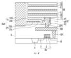
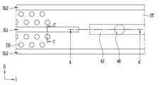
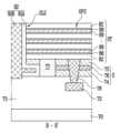
도 1a 내지 도 1d는 본 발명의 일 실시예에 따른 반도체 장치의 구조를 설명하기 위한 도면이다. 도 1a는 평면도이고, 도 1b 및 도 1c는 도 1a의 A-A' 단면도이고 도 1d는 도 1a의 C-C' 단면도이다.FIGS. 1A to 1D are drawings for explaining the structure of a semiconductor device according to one embodiment of the present invention. FIG. 1A is a plan view, FIGS. 1B and 1C are cross-sectional views taken along line A-A' of FIG. 1A, and FIG. 1D is a cross-sectional view taken along line C-C' of FIG. 1A.
도 1a, 도 1b 및 도 1d를 참조하면, 본 발명의 일 실시예에 따른 반도체 장치는 소스 구조(S1), 적층물(ST), 제1 슬릿 구조(SLI1) 및 제2 콘택 플러그(CP2)를 포함할 수 있다. 또한, 반도체 장치는 배선(UM), 제2 슬릿 구조(SLI2), 제1 콘택 플러그(CP1), 채널 구조(CH), 기판(10), 트랜지스터(TR) 또는 층간절연막(5) 중 적어도 하나를 더 포함할 수 있다.Referring to FIGS. 1A, 1B, and 1D, a semiconductor device according to an embodiment of the present invention may include a source structure (S1), a stacked structure (ST), a first slit structure (SLI1), and a second contact plug (CP2). In addition, the semiconductor device may further include at least one of a wiring (UM), a second slit structure (SLI2), a first contact plug (CP1), a channel structure (CH), a substrate (10), a transistor (TR), or an interlayer insulating film (5).
적층물(ST)은 교대로 적층된 도전막들(11) 및 절연막들(12)을 포함할 수 있다. 도전막들(11)은 워드라인, 선택 라인 등일 수 있다. 도전막들(11)은 폴리실리콘을 포함하거나, 텅스텐 등의 금속을 포함하거나, 이들을 조합하여 포함할 수 있다. 절연막들(12)은 도전막들(11)을 상호 절연시키기 위한 것이다. 절연막들(12)은 산화물, 질화물 등의 절연 물질을 포함할 수 있다. 또한, 적층물(ST)은 도전막들(11)과 절연막들(12)의 사이에 개재된 메모리막(13)을 더 포함할 수 있다. 메모리막(13)은 터널절연막, 데이터 저장막 또는 전하차단막 중 적어도 하나를 포함할 수 있다. 데이터 저장막은 플로팅 게이트, 전하 트랩 물질, 질화물, 나노 구조, 가변 저항 물질, 상변화 물질 등을 포함할 수 있다.The stack (ST) may include alternately stacked conductive films (11) and insulating films (12). The conductive films (11) may be word lines, selection lines, etc. The conductive films (11) may include polysilicon, a metal such as tungsten, or a combination thereof. The insulating films (12) are for mutually insulating the conductive films (11). The insulating films (12) may include an insulating material such as an oxide or a nitride. In addition, the stack (ST) may further include a memory film (13) interposed between the conductive films (11) and the insulating films (12). The memory film (13) may include at least one of a tunnel insulating film, a data storage film, or a charge blocking film. The data storage film may include a floating gate, a charge trap material, a nitride, a nanostructure, a variable resistance material, a phase change material, etc.
제1 슬릿 구조(SLI1)는 적층물(ST)을 관통하고 제1 방향(I)으로 확장될 수 있다. 제2 슬릿 구조(SLI2)는 적층물(ST)을 관통하고 제1 방향(I)으로 확장될 수 있다. 제1 슬릿 구조(SLI1)와 제2 슬릿 구조(SLI2)는 제2 방향(Ⅱ)으로 이웃할 수 있다. 제2 방향(Ⅱ)으로 이웃한 제2 슬릿 구조들(SLI2)의 사이에 제1 슬릿 구조(SLI1)가 위치될 수 있다. 여기서, 제2 방향(Ⅱ)은 제1 방향(I)과 교차된 방향일 수 있다.The first slit structure (SLI1) can penetrate the stack (ST) and extend in the first direction (I). The second slit structure (SLI2) can penetrate the stack (ST) and extend in the first direction (I). The first slit structure (SLI1) and the second slit structure (SLI2) can be adjacent in the second direction (II). The first slit structure (SLI1) can be positioned between the second slit structures (SLI2) adjacent in the second direction (II). Here, the second direction (II) can be a direction intersecting the first direction (I).
제1 슬릿 구조(SLI) 또는 제2 슬릿 구조들(SLI2)은 산화물, 질화물 등의 절연 물질을 포함할 수 있다. 또한, 제1 슬릿 구조(SLI) 또는 제2 슬릿 구조들(SLI2)은 소스 구조(S1)와 전기적으로 연결된 소스 콘택 구조(22)를 포함할 수 있다. 예를 들어, 제1 슬릿 구조(SLI)는 소스 콘택 구조(22) 및 소스 콘택 구조(22)의 측벽에 형성된 절연 스페이서(21)를 포함할 수 있다. 절연 스페이서(21)는 소스 콘택 구조(22)와 도전막들(11)을 절연시킬 수 있다.The first slit structure (SLI) or the second slit structures (SLI2) may include an insulating material such as an oxide or a nitride. In addition, the first slit structure (SLI) or the second slit structures (SLI2) may include a source contact structure (22) electrically connected to the source structure (S1). For example, the first slit structure (SLI) may include a source contact structure (22) and an insulating spacer (21) formed on a sidewall of the source contact structure (22). The insulating spacer (21) may insulate the source contact structure (22) and the conductive films (11).
채널 구조(CH)는 적층물(ST)을 관통하고 소스 구조(S1)와 연결될 수 있다. 채널 구조(CH)는 제1 슬릿 구조(SLI1)와 제2 슬릿 구조(SLI2)의 사이에 위치될 수 있다. 채널 구조(CH)는 채널막(34)을 포함할 수 있고, 메모리막(33), 갭필막(35) 등을 더 포함할 수 있다. 메모리막(33)은 터널절연막, 데이터 저장막 또는 전하차단막 중 적어도 하나를 포함할 수 있다. 데이터 저장막은 플로팅 게이트, 플로팅 게이트, 전하 트랩 물질, 질화물, 나노 구조, 가변 저항 물질, 상변화 물질 등을 포함할 수 있다.A channel structure (CH) can penetrate the stack (ST) and be connected to the source structure (S1). The channel structure (CH) can be positioned between the first slit structure (SLI1) and the second slit structure (SLI2). The channel structure (CH) can include a channel film (34) and can further include a memory film (33), a gap fill film (35), etc. The memory film (33) can include at least one of a tunnel insulating film, a data storage film, or a charge blocking film. The data storage film can include a floating gate, a floating gate, a charge trap material, a nitride, a nanostructure, a variable resistance material, a phase change material, etc.
채널 구조(CH)와 도전막들(11)이 교차된 위치에 메모리 셀, 선택 트랜지스터 등이 위치될 수 있다. 채널 구조(CH)를 공유하는 메모리 셀들 및 선택 트랜지스터들이 하나의 메모리 스트링을 구성할 수 있다. 예를 들어, 메모리 스트링은 적어도 하나의 드레인 선택 트랜지스터, 복수의 메모리 셀들 및 적어도 하나의 소스 선택 트랜지스터를 포함할 수 있다.Memory cells, selection transistors, etc. may be positioned at positions where the channel structure (CH) and the conductive films (11) intersect. Memory cells and selection transistors sharing the channel structure (CH) may form one memory string. For example, the memory string may include at least one drain selection transistor, a plurality of memory cells, and at least one source selection transistor.
소스 구조(S1)는 기판(10)과 적층물(ST)의 사이에 위치될 수 있다. 소스 구조(S1)는 단일막 또는 다층막일 수 있다. 소스 구조(S1)는 제3 소스막(18)을 포함할 수 있고, 제1 소스막(16) 또는 제2 소스막(17)을 더 포함할 수 있다. 제3 소스막(18)은 제1 소스막(16)과 제2 소스막(17)의 사이에 개재될 수 있다. 또한, 소스 구조(S1)는 제1 소스막(16)과 제2 소스막(17)의 사이에 개재된 희생막(19)을 더 포함할 수 있다. 소스 구조(S1)는 폴리실리콘을 포함하거나, 텅스텐과 같은 금속을 포함하거나, 이들을 조합하여 포함할 수 있다.The source structure (S1) may be positioned between the substrate (10) and the stack (ST). The source structure (S1) may be a single film or a multilayer film. The source structure (S1) may include a third source film (18) and may further include a first source film (16) or a second source film (17). The third source film (18) may be interposed between the first source film (16) and the second source film (17). In addition, the source structure (S1) may further include a sacrificial film (19) interposed between the first source film (16) and the second source film (17). The source structure (S1) may include polysilicon, a metal such as tungsten, or a combination thereof.
제1 슬릿 구조(SLI1) 또는 제2 슬릿 구조(SLI2)는 적층물(ST)을 관통하여 소스 구조(S1)의 내부로 확장될 수 있다. 예를 들어, 제1 슬릿 구조(SLI1) 또는 제2 슬릿 구조(SLI2)는 제2 소스막(17) 및 제3 소스막(18)을 관통하고, 제1 소스막(16)과 접할 수 있다.The first slit structure (SLI1) or the second slit structure (SLI2) may extend into the interior of the source structure (S1) by penetrating the stack (ST). For example, the first slit structure (SLI1) or the second slit structure (SLI2) may penetrate the second source film (17) and the third source film (18) and come into contact with the first source film (16).
제2 콘택 플러그(CP2)는 배선(UM)과 소스 구조(S1)를 전기적으로 연결시킬 수 있다. 제2 콘택 플러그(CP2)는 적층물(ST)과 배선(UM)의 사이에 위치될 수 있다. 제2 콘택 플러그(CP2)는 소스 구조(S1)를 관통할 수 있고, 소스 구조(S1)와 접할 수 있다. 소스 구조(S1)는 제2 콘택 플러그(CP2), 배선(UM) 및 제1 콘택 플러그(CP1)를 통해 제2 콘택 플러그(CP2)기판(10)과 전기적으로 연결될 수 있다.The second contact plug (CP2) can electrically connect the wiring (UM) and the source structure (S1). The second contact plug (CP2) can be located between the stack (ST) and the wiring (UM). The second contact plug (CP2) can penetrate the source structure (S1) and come into contact with the source structure (S1). The source structure (S1) can be electrically connected to the second contact plug (CP2) substrate (10) through the second contact plug (CP2), the wiring (UM), and the first contact plug (CP1).
제2 콘택 플러그(CP2)는 제2 소스막(17), 희생막(19) 및 제1 소스막(16)을 관통할 수 있다. 제2 콘택 플러그(CP2)는 제3 소스막(18)으로부터 이격하여 위치될 수 있고, 제2 콘택 플러그(CP2)과 제3 소스막(18)의 사이에 희생막(19)이 개재될 수 있다.The second contact plug (CP2) can penetrate the second source film (17), the sacrificial film (19), and the first source film (16). The second contact plug (CP2) can be positioned apart from the third source film (18), and a sacrificial film (19) can be interposed between the second contact plug (CP2) and the third source film (18).
제2 콘택 플러그(CP2)는 제1 슬릿 구조(SLI1)와 제1 방향(I)으로 이격되어 위치될 수 있다. 제1 방향(I) 및 제2 방향(Ⅱ)으로 정의된 평면에서, 제1 슬릿 구조(SLI1)와 제2 슬릿 구조(SLI2)는 제2 방향(Ⅱ)으로 제1 거리(D1) 이격될 수 있다. 제1 거리(D1)는 제1 슬릿 구조(SLI1)의 중심에서부터 제2 슬릿 구조(SLI2)의 중심까지의 거리이거나, 제1 슬릿 구조(SLI1)의 엣지부터 제2 슬릿 구조(SLI2)의 엣지까지의 거리일 수 있다. 상기 평면에서, 제1 슬릿 구조(SLI1)와 제2 콘택 플러그(CP2)은 제1 방향(I)으로 제2 거리(D2) 이격될 수 있다. 제2 거리(D2)는 제1 슬릿 구조(SLI1)의 엣지로부터 제2 콘택 플러그(CP2)의 엣지까지의 거리일 수 있다. 여기서, 제2 거리(D2)는 제1 거리(D1)에 비해 큰 값을 가질 수 있다. 제2 거리(D2)는 제1 거리(D1)의 2배 이상일 수 있다.The second contact plug (CP2) can be positioned spaced apart from the first slit structure (SLI1) in a first direction (I). In a plane defined by the first direction (I) and the second direction (II), the first slit structure (SLI1) and the second slit structure (SLI2) can be spaced apart from each other by a first distance (D1) in the second direction (II). The first distance (D1) can be a distance from a center of the first slit structure (SLI1) to a center of the second slit structure (SLI2), or a distance from an edge of the first slit structure (SLI1) to an edge of the second slit structure (SLI2). In the plane, the first slit structure (SLI1) and the second contact plug (CP2) can be spaced apart from each other by a second distance (D2) in the first direction (I). The second distance (D2) may be a distance from an edge of the first slit structure (SLI1) to an edge of the second contact plug (CP2). Here, the second distance (D2) may have a larger value than the first distance (D1). The second distance (D2) may be at least twice the first distance (D1).
기판(10)과 소스 구조(S1)의 사이에 층간절연막(5)이 개재될 수 있다. 층간절연막(5) 내에 주변 회로 및 주변 회로와 전기적으로 연결된 인터커넥션 구조가 위치될 수 있다. 주변 회로는 메모리 스트링을 구동하기 위한 것으로, 기판(10) 상에 위치될 수 있다. 주변 회로는 트랜지스터(TR), 캐패시터, 레지스터, 증폭기, 디코더, 전압 발생기 등을 포함할 수 있다. 트랜지스터(TR)는 게이트 절연막(1) 및 게이트 전극(2)을 포함할 수 있다. 게이트 전극(2) 양측의 기판(10) 내에 정션(3)이 형성될 수 있다. 또한, 기판(10) 내에 소자분리막(4)이 형성될 수 있다.An interlayer insulating film (5) may be interposed between the substrate (10) and the source structure (S1). A peripheral circuit and an interconnection structure electrically connected to the peripheral circuit may be positioned within the interlayer insulating film (5). The peripheral circuit is for driving a memory string and may be positioned on the substrate (10). The peripheral circuit may include a transistor (TR), a capacitor, a resistor, an amplifier, a decoder, a voltage generator, etc. The transistor (TR) may include a gate insulating film (1) and a gate electrode (2). A junction (3) may be formed within the substrate (10) on both sides of the gate electrode (2). In addition, a device isolation film (4) may be formed within the substrate (10).
인터커넥션 구조는 제2 콘택 플러그(CP2), 배선(UM) 또는 제1 콘택 플러그(CP1) 중 적어도 하나를 포함할 수 있다. 제1 콘택 플러그(CP1)는 기판(10)과 배선(UM)의 사이에 위치될 수 있다. 제1 콘택 플러그(CP1)는 주변 회로와 전기적으로 연결되거나, 기판(10)의 정션(3)과 전기적으로 연결될 수 있다.The interconnection structure may include at least one of a second contact plug (CP2), a wiring (UM), or a first contact plug (CP1). The first contact plug (CP1) may be positioned between the substrate (10) and the wiring (UM). The first contact plug (CP1) may be electrically connected to a peripheral circuit or electrically connected to a junction (3) of the substrate (10).
제2 콘택 플러그(CP2)는 디스차지 콘택 플러그일 수 있다. 소스 구조(S1) 내에 존재하는 전하가 제2 콘택 플러그(CP2), 배선(UM) 및 제1 콘택 플러그(CP1)를 통해 기판(10)으로 방출될 수 있다. 따라서, 소스 구조(S1) 내에 전하가 축적되지 않고, 축적된 전하로 인해 반도체 장치가 손상되는 것을 방지할 수 있다.The second contact plug (CP2) may be a discharge contact plug. Charges existing in the source structure (S1) may be discharged to the substrate (10) through the second contact plug (CP2), the wiring (UM), and the first contact plug (CP1). Accordingly, charges may not be accumulated in the source structure (S1), and damage to the semiconductor device due to the accumulated charges may be prevented.
도 1c는 도 1b와 유사하되, 제1 슬릿 구조(SLI1')가 제1 돌출부(P1)를 포함하는 경우를 나타낸다. 도 1a 및 도 1c를 참조하면, 제1 슬릿 구조(SLI1')는 제1 관통부(T1) 및 제1 돌출부(P1)를 포함할 수 있다. 제1 관통부(T1)는 적층물(ST) 및 소스 구조(S1')를 관통할 수 있다. 제1 돌출부(P1)는 제1 관통부(T1)의 측벽으로부터 소스 구조(S1')의 내부로 돌출될 수 있다. 제2 콘택 플러그(CP2)는 제1 돌출부(P1)로부터 이격될 수 있다. 제2 콘택 플러그(CP2)와 제1 돌출부(P1)의 사이에 희생막(19) 및 제1 소스막(16)이 개재될 수 있다. 본 도면에는 도시되지 않았으나, 제1 슬릿 구조(SLI1')는 제1 돌출부(P1) 내에 위치된 보이드를 포함할 수 있다.FIG. 1C is similar to FIG. 1B, but illustrates a case where the first slit structure (SLI1') includes a first protrusion (P1). Referring to FIGS. 1A and 1C, the first slit structure (SLI1') may include a first through-hole (T1) and a first protrusion (P1). The first through-hole (T1) may penetrate the stack (ST) and the source structure (S1'). The first protrusion (P1) may protrude from a sidewall of the first through-hole (T1) into the interior of the source structure (S1'). A second contact plug (CP2) may be spaced apart from the first protrusion (P1). A sacrificial film (19) and a first source film (16) may be interposed between the second contact plug (CP2) and the first protrusion (P1). Although not shown in the drawing, the first slit structure (SLI1') may include a void located within the first protrusion (P1).
제1 슬릿 구조(SLI1')는 절연 스페이서 및 소스 콘택 구조를 포함할 수 있다. 절연 스페이서는 관통부(21B) 및 관통부(21B)의 측벽으로부터 돌출된 돌출부(21A)를 포함할 수 있다. 소스 콘택 구조는 관통부(22B) 및 관통부(22B)의 측벽으로부터 돌출된 돌출부(22A)를 포함할 수 있다. 본 도면에는 도시되지 않았으나, 제1 슬릿 구조(SLI1')는 돌출부(22A) 내에 위치된 보이드를 포함할 수 있다.The first slit structure (SLI1') may include an insulating spacer and a source contact structure. The insulating spacer may include a through-hole (21B) and a protrusion (21A) protruding from a sidewall of the through-hole (21B). The source contact structure may include a through-hole (22B) and a protrusion (22A) protruding from a sidewall of the through-hole (22B). Although not shown in the drawing, the first slit structure (SLI1') may include a void located within the protrusion (22A).
전술한 바와 같은 구조에 따르면, 제2 콘택 플러그(CP2)가 제1 슬릿 구조(SLI1) 또는 제1 슬릿 구조(SLI1')의 제1 돌출부(P1)로부터 충분히 이격되어 위치될 수 있다. 제2 콘택 플러그(CP2)따라서, 제조 과정에서 제2 콘택 플러그(CP2)가 노출되거나 손상되는 것을 방지할 수 있다.According to the structure as described above, the second contact plug (CP2) can be positioned sufficiently spaced apart from the first protrusion (P1) of the first slit structure (SLI1) or the first slit structure (SLI1'). Therefore, the second contact plug (CP2) can be prevented from being exposed or damaged during the manufacturing process.
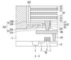
도 2a 내지 도 2c는 본 발명의 일 실시예에 따른 반도체 장치의 구조를 설명하기 위한 도면이다. 도 2a는 평면도이고, 도 2b 및 도 2c는 도 2a의 A-A' 단면도이다. 이하 앞서 설명된 내용과 중복된 내용은 생략하여 설명하도록 한다.FIGS. 2A to 2C are drawings for explaining the structure of a semiconductor device according to one embodiment of the present invention. FIG. 2A is a plan view, and FIGS. 2B and 2C are cross-sectional views taken along line A-A' of FIG. 2A. Any content that overlaps with the previously explained content will be omitted for explanation.
도 2a 및 도 2b를 참조하면, 본 발명의 일 실시예에 따른 반도체 장치는 소스 구조(S2), 적층물(ST), 제1 슬릿 구조(SLI1) 및 제2 콘택 플러그(CP2)를 포함할 수 있다. 또한, 반도체 장치는 배선(UM), 제2 슬릿 구조(SLI2), 제3 슬릿 구조(SLI3), 제1 콘택 플러그(CP1), 채널 구조(CH), 기판(10), 트랜지스터(TR) 또는 층간절연막(5) 중 적어도 하나를 더 포함할 수 있다.Referring to FIGS. 2A and 2B, a semiconductor device according to an embodiment of the present invention may include a source structure (S2), a stacked structure (ST), a first slit structure (SLI1), and a second contact plug (CP2). In addition, the semiconductor device may further include at least one of a wiring (UM), a second slit structure (SLI2), a third slit structure (SLI3), a first contact plug (CP1), a channel structure (CH), a substrate (10), a transistor (TR), or an interlayer insulating film (5).
제3 슬릿 구조(SLI3)는 적층물(ST)을 관통하고, 제1 슬릿 구조(SLI1)과 교차할 수 있다. 제3 슬릿 구조(SLI3)의 형태는 다양하게 변경될 수 있다. 제1 방향(I) 및 제2 방향(Ⅱ)으로 정의된 평면에서, 제3 슬릿 구조(SLI3)는 섬 형태를 갖거나, 제2 방향(Ⅱ)으로 확장된 라인 형태를 갖거나, C 형태를 가질 수 있다. 또한, 제3 슬릿 구조(SLI3)는 제1 방향(I)으로 돌출된 적어도 하나의 돌출부를 포함할 수 있다. 제2 방향(Ⅱ)으로 이웃한 제2 슬릿 구조들(SLI2)의 사이에 제1 슬릿 구조(SLI1) 및 제3 슬릿 구조(SLI3)가 위치될 수 있다.The third slit structure (SLI3) can penetrate the stack (ST) and intersect with the first slit structure (SLI1). The shape of the third slit structure (SLI3) can be variously changed. In a plane defined by the first direction (I) and the second direction (II), the third slit structure (SLI3) can have an island shape, a line shape extended in the second direction (II), or a C shape. In addition, the third slit structure (SLI3) can include at least one protrusion protruding in the first direction (I). The first slit structure (SLI1) and the third slit structure (SLI3) can be positioned between adjacent second slit structures (SLI2) in the second direction (II).
제1 슬릿 구조(SLI1)는 제3 슬릿 구조(SLI3)와 중첩된 부분(P)을 포함할 수 있다. 평면에서, 제1 슬릿 구조(SLI1)가 제3 슬릿 구조(SLI3)의 내부로 돌출될 수 있다. 단면에서, 제3 슬릿 구조(SLI3)는 소스 구조(S2) 내로 돌출될 수 있다. 예를 들어, 제3 슬릿 구조(SLI3)는 제2 소스막(17)을 관통하고, 제3 소스막(18)과 접할 수 있다. 제3 슬릿 구조(SLI3)는 제1 슬릿 구조(SLI1) 또는 제2 슬릿 구조(SLI2)에 비해 얕은 깊이를 가질 수 있다.The first slit structure (SLI1) may include a portion (P) overlapping with the third slit structure (SLI3). In a plan view, the first slit structure (SLI1) may protrude into the interior of the third slit structure (SLI3). In a cross-section, the third slit structure (SLI3) may protrude into the source structure (S2). For example, the third slit structure (SLI3) may penetrate the second source film (17) and contact the third source film (18). The third slit structure (SLI3) may have a shallower depth than the first slit structure (SLI1) or the second slit structure (SLI2).
도 2c는 도 2b와 유사하되, 제1 슬릿 구조(SLI1')가 제1 돌출부(P1)를 포함하는 경우를 나타낸다. 도 2a 및 도 2c를 참조하면, 제1 슬릿 구조(SLI1')는 제1 관통부(T1) 및 제1 돌출부(P1)를 포함할 수 있다. 절연 스페이서는 관통부(21B) 및 돌출부(21A)를 포함할 수 있다. 소스 콘택 구조는 관통부(22B) 및 돌출부(22A)를 포함할 수 있다. 제2 콘택 플러그(CP2)는 제1 돌출부(P1)로부터 이격될 수 있다. 제2 콘택 플러그(CP2)와 제1 돌출부(P1)의 사이에 희생막(19) 및 제1 소스막(16)이 개재될 수 있다.FIG. 2C is similar to FIG. 2B, but illustrates a case where the first slit structure (SLI1') includes a first protrusion (P1). Referring to FIGS. 2A and 2C, the first slit structure (SLI1') may include a first through-hole (T1) and a first protrusion (P1). The insulating spacer may include a through-hole (21B) and a protrusion (21A). The source contact structure may include a through-hole (22B) and a protrusion (22A). The second contact plug (CP2) may be spaced apart from the first protrusion (P1). A sacrificial film (19) and a first source film (16) may be interposed between the second contact plug (CP2) and the first protrusion (P1).
전술한 바와 같은 구조에 따르면, 제1 슬릿 구조(SLI1')와 제3 슬릿 구조(SLI3)가 중첩된다. 또한, 중첩 부분(P) 또는 그 주변에 제1 돌출부(P1)가 위치될 수 있다. 제2 콘택 플러그(CP2)가 제1 슬릿 구조(SLI1) 또는 제1 슬릿 구조(SLI1')의 제1 돌출부(P1)로부터 충분히 이격되어 위치되므로, 제조 과정에서 제2 콘택 플러그(CP2)가 노출되거나 손상되는 것을 방지할 수 있다.According to the structure described above, the first slit structure (SLI1') and the third slit structure (SLI3) overlap. In addition, a first protrusion (P1) may be positioned at or around the overlapping portion (P). Since the second contact plug (CP2) is positioned sufficiently spaced apart from the first slit structure (SLI1) or the first protrusion (P1) of the first slit structure (SLI1'), the second contact plug (CP2) can be prevented from being exposed or damaged during the manufacturing process.
도 3a 내지 도 3c는 본 발명의 일 실시예에 따른 반도체 장치의 구조를 설명하기 위한 도면이다. 도 3a는 평면도이고, 도 3b 및 도 3c는 도 3a의 B-B' 단면도이다. 이하 앞서 설명된 내용과 중복된 내용은 생략하여 설명하도록 한다.FIGS. 3A to 3C are drawings for explaining the structure of a semiconductor device according to one embodiment of the present invention. FIG. 3A is a plan view, and FIGS. 3B and 3C are cross-sectional views taken along line B-B' of FIG. 3A. Any content that overlaps with the previously explained content will be omitted for explanation.
도 3a 및 도 3b를 참조하면, 본 발명의 일 실시예에 따른 반도체 장치는 소스 구조(S3), 적층물(ST), 제1 슬릿 구조(SLI1) 및 제2 콘택 플러그(CP2)를 포함할 수 있다. 반도체 장치는 배선(UM), 제2 슬릿 구조(SLI2), 제1 콘택 플러그(CP1), 채널 구조(CH), 분리막(15), 기판(10), 트랜지스터(TR) 또는 층간절연막(5) 중 적어도 하나를 더 포함할 수 있다. 또한, 본 도면에는 도시되지 않았으나, 반도체 장치는 제3 슬릿 구조(도 2a 참조)를 더 포함할 수 있다.Referring to FIGS. 3A and 3B, a semiconductor device according to an embodiment of the present invention may include a source structure (S3), a stack (ST), a first slit structure (SLI1), and a second contact plug (CP2). The semiconductor device may further include at least one of a wiring (UM), a second slit structure (SLI2), a first contact plug (CP1), a channel structure (CH), a separator (15), a substrate (10), a transistor (TR), or an interlayer insulating film (5). In addition, although not illustrated in the drawings, the semiconductor device may further include a third slit structure (see FIG. 2A).
제2 슬릿 구조(SLI2)는 소스 콘택 구조(24) 및 소스 콘택 구조(24)의 측벽에 형성된 절연 스페이서(23)를 포함할 수 있다. 절연 스페이서(23)는 소스 콘택 구조(24)와 도전막들(11)을 절연시킬 수 있다.The second slit structure (SLI2) may include a source contact structure (24) and an insulating spacer (23) formed on a sidewall of the source contact structure (24). The insulating spacer (23) may insulate the source contact structure (24) and the conductive films (11).
분리막(15)은 제2 슬릿 구조(SLI2)와 제2 콘택 플러그(CP2)의 사이에 위치될 수 있다. 분리막(15)은 제1 방향(I)으로 확장될 수 있다. 분리막(15)은 소스 구조(S3)와 실질적으로 동일한 레벨에 위치될 수 있다. 분리막(15)은 산화물, 질화물 등의 절연 물질을 포함할 수 있다.The separator (15) may be positioned between the second slit structure (SLI2) and the second contact plug (CP2). The separator (15) may extend in the first direction (I). The separator (15) may be positioned at substantially the same level as the source structure (S3). The separator (15) may include an insulating material such as an oxide or a nitride.
제2 콘택 플러그(CP2)는 제2 슬릿 구조(SLI2)와 제2 방향(Ⅱ)으로 이격되어 위치될 수 있다. 제1 방향(I) 및 제2 방향(Ⅱ)으로 정의된 평면에서, 제1 슬릿 구조(SLI1)와 제2 슬릿 구조(SLI2)는 제2 방향(Ⅱ)으로 제1 거리(D1) 이격될 수 있다. 상기 평면에서, 분리막(15)의 엣지와 제2 콘택 플러그(CP2)는 제3 거리(D3) 이격될 수 있다. 제3 거리(D3)는 분리막(15)의 엣지로부터 제2 콘택 플러그(CP2)의 엣지까지의 거리일 수 있다. 여기서, 제3 거리(D3)는 제1 거리(D1)에 비해 큰 값을 가질 수 있다. 제3 거리(D3)는 제1 거리(D1)의 2배 이상일 수 있다.The second contact plug (CP2) may be positioned spaced apart from the second slit structure (SLI2) in a second direction (II). In a plane defined by the first direction (I) and the second direction (II), the first slit structure (SLI1) and the second slit structure (SLI2) may be spaced apart from each other by a first distance (D1) in the second direction (II). In the plane, the edge of the separator (15) and the second contact plug (CP2) may be spaced apart from each other by a third distance (D3). The third distance (D3) may be a distance from the edge of the separator (15) to the edge of the second contact plug (CP2). Here, the third distance (D3) may have a larger value than the first distance (D1). The third distance (D3) may be at least twice the first distance (D1).
도 3c는 도 3b와 유사하되, 제2 슬릿 구조(SLI2')가 제2 돌출부(P2)를 포함하는 경우를 나타낸다. 도 3a 및 도 3c를 참조하면, 제2 슬릿 구조(SLI2')는 제2 관통부(T2) 및 제2 돌출부(P2)를 포함할 수 있다. 제2 관통부(T2)는 적층물(ST) 및 소스 구조(S3')를 관통할 수 있다. 제2 돌출부(P2)는 제2 관통부(T2)의 측벽으로부터 소스 구조(S3')의 내부로 돌출될 수 있다. 제2 콘택 플러그(CP2)는 제2 돌출부(P2)로부터 이격될 수 있다. 제2 콘택 플러그(CP2)와 제2 돌출부(P2)의 사이에 분리막(15), 희생막(19) 및 제1 소스막(16)이 개재될 수 있다.FIG. 3c is similar to FIG. 3b, but illustrates a case where the second slit structure (SLI2') includes a second protrusion (P2). Referring to FIGS. 3a and 3c, the second slit structure (SLI2') may include a second penetration portion (T2) and a second protrusion portion (P2). The second penetration portion (T2) may penetrate the stack (ST) and the source structure (S3'). The second protrusion portion (P2) may protrude from a sidewall of the second penetration portion (T2) into the interior of the source structure (S3'). The second contact plug (CP2) may be spaced apart from the second protrusion portion (P2). A separator (15), a sacrificial film (19), and a first source film (16) may be interposed between the second contact plug (CP2) and the second protrusion portion (P2).
제2 슬릿 구조(SLI2')는 절연 스페이서 및 소스 콘택 구조를 포함할 수 있다. 절연 스페이서는 관통부(23B) 및 관통부(23B)의 측벽으로부터 돌출된 돌출부(23A)를 포함할 수 있다. 소스 콘택 구조는 관통부(24B) 및 관통부(24B)의 측벽으로부터 돌출된 돌출부(24A)를 포함할 수 있다.The second slit structure (SLI2') may include an insulating spacer and a source contact structure. The insulating spacer may include a through-hole (23B) and a protrusion (23A) protruding from a sidewall of the through-hole (23B). The source contact structure may include a through-hole (24B) and a protrusion (24A) protruding from a sidewall of the through-hole (24B).
전술한 바와 같은 구조에 따르면, 분리막(15)에 의해 제2 슬릿 구조(SLI2)와 제2 콘택 플러그(CP2)를 이격시키거나, 제2 슬릿 구조(SLI2')의 제2 돌출부(P2)와 제2 콘택 플러그(CP2)를 이격시킬 수 있다. 따라서, 제조 과정에서 제2 콘택 플러그(CP2)가 노출되거나 손상되는 것을 방지할 수 있다.According to the structure described above, the second slit structure (SLI2) and the second contact plug (CP2) can be separated by the separator (15), or the second protrusion (P2) of the second slit structure (SLI2') and the second contact plug (CP2) can be separated. Accordingly, the second contact plug (CP2) can be prevented from being exposed or damaged during the manufacturing process.
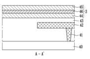
도 4a 내지 도 10a, 도 4b 내지 도 10b, 도 6c 내지 도 10c는 본 발명의 일 실시예에 따른 반도체 장치의 제조 방법을 설명하기 위한 도면이다. 각 번호의 a도는 평면도이고, 각 번호의 b도는 a도의 A-A' 단면도이고, 각 번호의 c도는 a도의 C-C' 단면도이다.FIGS. 4A to 10A, FIGS. 4B to 10B, and FIGS. 6C to 10C are drawings for explaining a method for manufacturing a semiconductor device according to one embodiment of the present invention. Drawing a of each number is a plan view, Drawing b of each number is a cross-sectional view taken along line A-A' of Drawing a, and Drawing c of each number is a cross-sectional view taken along line C-C' of Drawing a.
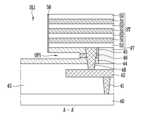
도 4a 및 도 4b를 참조하면, 베이스(40) 상에 인터커넥션 구조 및 층간절연막(43)을 형성한다. 베이스(40)는 기판, 주변 회로 등을 포함할 수 있다. 인터커넥션 구조는 제1 콘택 플러그(41), 배선(42) 등을 포함할 수 있다. 인터커넥션 구조는 층간절연막(43) 내에 형성될 수 있고, 베이스(40)와 전기적으로 연결될 수 있다. 예를 들어, 제1 콘택 플러그(41)가 주변 회로, 기판 등과 전기적으로 연결될 수 있다. 층간절연막(43)은 단일막 또는 다층막일 수 있다.Referring to FIGS. 4A and 4B, an interconnection structure and an interlayer insulating film (43) are formed on a base (40). The base (40) may include a substrate, peripheral circuits, etc. The interconnection structure may include a first contact plug (41), a wiring (42), etc. The interconnection structure may be formed within the interlayer insulating film (43) and may be electrically connected to the base (40). For example, the first contact plug (41) may be electrically connected to a peripheral circuit, a substrate, etc. The interlayer insulating film (43) may be a single film or a multilayer film.
이어서, 층간절연막(43) 상에 소스 구조(S)를 형성한다. 소스 구조(S)는 단일막 또는 다층막을 포함할 수 있다. 소스 구조(S)는 희생막(46)을 포함할 수 있다. 소스 구조(S)는 제1 소스막(44) 또는 제2 소스막(45)을 더 포함할 수 있다. 희생막(46)은 제1 소스막(44)과 제2 소스막(45)의 사이에 개재될 수 있다. 희생막(46)은 단일막이거나 다층막일 수 있다.Next, a source structure (S) is formed on the interlayer insulating film (43). The source structure (S) may include a single film or a multilayer film. The source structure (S) may include a sacrificial film (46). The source structure (S) may further include a first source film (44) or a second source film (45). The sacrificial film (46) may be interposed between the first source film (44) and the second source film (45). The sacrificial film (46) may be a single film or a multilayer film.
제1 소스막(44) 및 제2 소스막(45)은 폴리실리콘, 텅스텐 등의 도전막을 포함할 수 있다. 희생막(46)은 폴리실리콘막, 산화물, 질화물 등을 포함할 수 있다.The first source film (44) and the second source film (45) may include a conductive film such as polysilicon, tungsten, etc. The sacrificial film (46) may include a polysilicon film, oxide, nitride, etc.
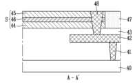
도 5a 및 도 5b를 참조하면, 소스 구조(S)를 패터닝한다. 소스 구조(S)를 식각하여 트렌치를 형성한 후, 트렌치 내에 분리막(47)을 형성한다. 분리막(47)의 개수, 위치, 형태 등은 다양하게 변경될 수 있다. 분리막(47)은 소스 구조(S)를 메모리 블록 단위로 분리하기 위한 것이거나, 캐비티의 위치를 제한하기 위한 배리어일 수 있다. 메모리 블록은 소거 동작이 수행되는 단위일 수 있고, 메모리 블록은 복수의 메모리 스트링들을 포함할 수 있다.Referring to FIGS. 5A and 5B, the source structure (S) is patterned. After the source structure (S) is etched to form a trench, a separation film (47) is formed within the trench. The number, position, shape, etc. of the separation film (47) may be variously changed. The separation film (47) may be for separating the source structure (S) into memory block units or may be a barrier for limiting the position of the cavity. The memory block may be a unit in which an erase operation is performed, and the memory block may include a plurality of memory strings.
이어서, 제2 콘택 플러그(48)를 형성한다. 예를 들어, 소스 구조(S)를 관통하고 배선(42)을 노출시키는 콘택 홀을 형성한 후, 콘택 홀 내에 도전막을 채워 제2 콘택 플러그(48)를 형성한다. 제2 콘택 플러그(48)는 소스 구조(S)를 관통할 수 있고, 배선(42)과 연결될 수 있다. 소스 구조(S)가 제2 콘택 플러그(48), 배선(42) 및 제1 콘택 플러그(41)를 통해 베이스(40)와 전기적으로 연결될 수 있다.Next, a second contact plug (48) is formed. For example, after forming a contact hole that penetrates the source structure (S) and exposes the wiring (42), a conductive film is filled in the contact hole to form the second contact plug (48). The second contact plug (48) can penetrate the source structure (S) and be connected to the wiring (42). The source structure (S) can be electrically connected to the base (40) through the second contact plug (48), the wiring (42), and the first contact plug (41).
배선(42) 및 제2 콘택 플러그(48)의 위치는 후속 공정에서 형성되는 제1 슬릿(SL1) 또는 제2 슬릿(SL)의 위치를 고려하여 결정될 수 있다. 배선(42) 및 제2 콘택 플러그(48)는 제1 슬릿(SL1) 또는 제2 슬릿(SL2)으로 충분히 이격되도록 위치될 수 있다.The positions of the wiring (42) and the second contact plug (48) can be determined by considering the positions of the first slit (SL1) or the second slit (SL) formed in a subsequent process. The wiring (42) and the second contact plug (48) can be positioned to be sufficiently spaced apart from the first slit (SL1) or the second slit (SL2).
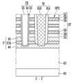
도 6a 내지 도 6c를 참조하면, 적층물(ST)을 형성한다. 적층물(ST)은 교대로 적층된 제1 물질막들(51) 및 제2 물질막들(52)을 포함할 수 있다. 제1 물질막들(51)은 메모리 셀, 선택 트랜지스터 등의 게이트 전극을 형성하기 위한 것일 수 있고, 제2 물질막들(52)은 적층된 게이트 전극들을 상호 절연시키기 위한 것일 수 있다.Referring to FIGS. 6A to 6C, a laminate (ST) is formed. The laminate (ST) may include first material films (51) and second material films (52) that are alternately laminated. The first material films (51) may be for forming a gate electrode of a memory cell, a selection transistor, or the like, and the second material films (52) may be for mutually insulating the laminated gate electrodes.
제1 물질막들(51)은 제2 물질막들(52)에 대해 식각 선택비가 높은 물질을 포함한다. 일 예로, 제1 물질막들(51)은 질화물 등을 포함하는 희생막일 수 있고, 제2 물질막들(52)은 산화물 등을 포함하는 절연막일 수 있다. 다른 예로, 제1 물질막들(51)은 폴리실리콘, 텅스텐 등을 포함하는 도전막일 수 있고, 제2 물질막들(52)은 산화물 등을 포함하는 절연막일 수 있다.The first material films (51) include a material having a high etching selectivity with respect to the second material films (52). For example, the first material films (51) may be a sacrificial film including a nitride or the like, and the second material films (52) may be an insulating film including an oxide or the like. As another example, the first material films (51) may be a conductive film including polysilicon, tungsten or the like, and the second material films (52) may be an insulating film including an oxide or the like.
이어서, 채널 구조들(CH)을 형성한다. 채널 구조들(CH)은 적층물(ST)을 관통할 수 있다. 채널 구조들(CH)은 소스 구조(S) 내로 돌출될 수 있다. 채널 구조들(CH) 각각은 채널막(54)을 포함할 수 있고, 제1 메모리막(53) 또는 갭필막(55)을 더 포함할 수 있다. 제1 메모리막(53)은 전하차단막, 데이터저장막 또는 터널절연막 중 적어도 하나를 포함할 수 있다.Next, channel structures (CH) are formed. The channel structures (CH) can penetrate the stack (ST). The channel structures (CH) can protrude into the source structure (S). Each of the channel structures (CH) can include a channel film (54) and further include a first memory film (53) or a gapfill film (55). The first memory film (53) can include at least one of a charge blocking film, a data storage film, or a tunnel insulating film.
이어서, 적층물(ST)을 관통하는 제1 슬릿(SL1)을 형성한다. 제1 슬릿(SL1)은 적층물(ST)을 관통할 수 있고, 제1 방향(I)으로 확장될 수 있다. 제1 슬릿(SL1)과 제2 콘택 플러그(48)은 제1 방향(I)으로 이웃할 수 있다. 제1 슬릿(SL1)은 소스 구조(S)의 표면을 노출시키는 깊이로 형성되거나, 소스 구조(S)를 일부 관통하는 깊이로 형성될 수 있다. 제1 슬릿(SL1)은 희생막(46)을 노출시키는 깊이로 형성될 수 있다.Next, a first slit (SL1) penetrating the stack (ST) is formed. The first slit (SL1) can penetrate the stack (ST) and extend in the first direction (I). The first slit (SL1) and the second contact plug (48) can be adjacent to each other in the first direction (I). The first slit (SL1) can be formed to a depth that exposes a surface of the source structure (S) or to a depth that partially penetrates the source structure (S). The first slit (SL1) can be formed to a depth that exposes the sacrificial film (46).
적층물(ST)을 관통하는 제2 슬릿(SL2)을 형성한다. 제2 슬릿(SL2)은 적층물(ST)을 관통할 수 있고, 제1 방향(I)으로 확장될 수 있다. 제2 슬릿(SL2)과 제2 콘택 플러그(48)은 제2 방향(Ⅱ)으로 이웃할 수 있다. 제1 슬릿(SL1)을 형성할 때 제2 슬릿(SL2)을 형성할 수 있다. 제2 슬릿(SL2)은 제1 슬릿(SL1)과 실질적으로 동일한 깊이를 가질 수 있다. 제2 방향(Ⅱ)으로 이웃한 제1 슬릿(SL1)과 제2 슬릿(SL2)의 사이에 채널 구조들(CH)이 위치될 수 있다.A second slit (SL2) penetrating the stack (ST) is formed. The second slit (SL2) can penetrate the stack (ST) and can extend in a first direction (I). The second slit (SL2) and the second contact plug (48) can be adjacent in the second direction (II). The second slit (SL2) can be formed when the first slit (SL1) is formed. The second slit (SL2) can have substantially the same depth as the first slit (SL1). Channel structures (CH) can be positioned between the first slit (SL1) and the second slit (SL2) adjacent in the second direction (II).
제1 방향(I) 및 제2 방향(Ⅱ)으로 정의된 평면에서, 제1 슬릿(SL1)과 제2 슬릿(SL2)은 제2 방향(Ⅱ)으로 제1 거리(D1) 이격될 수 있다. 상기 평면에서, 제1 슬릿(SL1)과 제2 콘택 플러그(48)은 제1 방향(I)으로 제2 거리(D2) 이격될 수 있다. 제2 거리(D2)는 제1 슬릿(SL1)의 엣지로부터 제2 콘택 플러그(48)의 엣지까지의 거리일 수 있다. 여기서, 제2 거리(D2)는 제1 거리(D1)에 비해 큰 값을 가질 수 있다. 제2 거리(D2)는 제1 거리(D1)의 2배 이상일 수 있다.In a plane defined by a first direction (I) and a second direction (II), the first slit (SL1) and the second slit (SL2) can be spaced apart from each other by a first distance (D1) in the second direction (II). In the plane, the first slit (SL1) and the second contact plug (48) can be spaced apart from each other by a second distance (D2) in the first direction (I). The second distance (D2) can be a distance from an edge of the first slit (SL1) to an edge of the second contact plug (48). Here, the second distance (D2) can have a larger value than the first distance (D1). The second distance (D2) can be twice or more the first distance (D1).
참고로, 제1 슬릿(SL1) 및 제2 슬릿(SL2)을 형성하기 전에 제3 슬릿 구조(도 2a의 제3 슬릿 구조 참조)를 형성하는 것도 가능하다. 이러한 경우, 제3 슬릿 구조와 교차되도록 제1 슬릿(SL1)을 형성할 수 있다.For reference, it is also possible to form the third slit structure (see the third slit structure in Fig. 2a) before forming the first slit (SL1) and the second slit (SL2). In this case, the first slit (SL1) can be formed to intersect with the third slit structure.
이어서, 제1 슬릿(SL1)의 내벽에 보호막(56)을 형성할 수 있다. 보호막(56)은 희생막(46)에 대해 식각 선택비가 높은 물질을 포함할 수 있다. 희생막(46)이 폴리실리콘을 포함하고 보호막(56)이 질화물, 산화물 등을 포함할 수 있다. 희생막(46)이 질화물, 산화물 등을 포함하고 보호막(56)이 폴리실리콘을 포함할 수 있다. 보호막(56)은 제2 슬릿(SL2)의 내벽에도 형성될 수 있다.Next, a protective film (56) may be formed on the inner wall of the first slit (SL1). The protective film (56) may include a material having a high etching selectivity with respect to the sacrificial film (46). The sacrificial film (46) may include polysilicon, and the protective film (56) may include a nitride, an oxide, or the like. The sacrificial film (46) may include a nitride, an oxide, or the like, and the protective film (56) may include polysilicon. The protective film (56) may also be formed on the inner wall of the second slit (SL2).
도 7a 내지 도 7c를 참조하면, 제1 슬릿(SL1) 또는 제2 슬릿(SL2)을 통해 희생막(46)을 제거하여 제1 개구부(OP1)를 형성한다. 희생막(46)을 선택적으로 식각하여 제1 개구부(OP1)를 형성할 수 있다. 희생막(46)을 식각할 때, 보호막(56)에 의해 제1 물질막들(51) 및 제2 물질막들(52)을 보호할 수 있다.Referring to FIGS. 7A to 7C, a first opening (OP1) is formed by removing the sacrificial film (46) through the first slit (SL1) or the second slit (SL2). The first opening (OP1) can be formed by selectively etching the sacrificial film (46). When etching the sacrificial film (46), the first material films (51) and the second material films (52) can be protected by the protective film (56).
제1 슬릿(SL1)을 통해 유입된 식각 조성물에 의해 희생막(46)이 식각될 수 있다. 제1 슬릿(SL1)과 인접한 영역의 희생막(46)이 식각될 수 있고, 제1 슬릿(SL1)과 이격된 영역의 희생막(46)은 잔류될 수 있다. 채널 구조(CH)는 제1 슬릿(SL1)과 인접하여 위치하므로, 제1 개구부(OP1)를 통해 제1 메모리막(53)이 노출될 수 있다. 반면에, 제2 콘택 플러그(48)는 제1 슬릿(SL1)으로부터 이격되어 있으므로, 제2 콘택 플러그(48) 주변의 희생막(46)은 잔류될 수 있다. 따라서, 제2 콘택플러그(48)는 제1 개구부(OP1)를 통해 노출되지 않는다. 참고로, 제2 슬릿(SL2)을 통해서도 식각 조성물이 유입될 수 있으며, 제2 슬릿(SL2)을 통해 희생막(46)을 제거하여 제1 개구부(OP1)를 형성할 수 있다.The sacrificial film (46) can be etched by the etching composition introduced through the first slit (SL1). The sacrificial film (46) in the area adjacent to the first slit (SL1) can be etched, and the sacrificial film (46) in the area spaced apart from the first slit (SL1) can remain. Since the channel structure (CH) is positioned adjacent to the first slit (SL1), the first memory film (53) can be exposed through the first opening (OP1). On the other hand, since the second contact plug (48) is spaced apart from the first slit (SL1), the sacrificial film (46) around the second contact plug (48) can remain. Therefore, the second contact plug (48) is not exposed through the first opening (OP1). For reference, the etching composition can also be introduced through the second slit (SL2), and the sacrificial film (46) can be removed through the second slit (SL2) to form the first opening (OP1).
이어서, 제1 개구부(OP1)를 통해 노출된 제1 메모리막(53)을 식각한다. 이를 통해, 채널막(54)이 노출된다. 제1 메모리막(53)을 식각할 때, 보호막(56)에 의해 제1 물질막들(51) 및 제2 물질막들(52)을 보호할 수 있다.Next, the first memory film (53) exposed through the first opening (OP1) is etched. Through this, the channel film (54) is exposed. When etching the first memory film (53), the first material films (51) and the second material films (52) can be protected by the protective film (56).
도 8a 내지 도 8c를 참조하면, 제1 개구부(OP1)를 채우도록 도전막(57)을 형성한다. 도전막(57)은 제1 슬릿(SL1) 또는 제2 슬릿(SL2) 내에도 형성될 수 있다. 도전막(57)은 폴리실리콘, 금속 등의 도전 물질을 포함할 수 있다.Referring to FIGS. 8A to 8C, a conductive film (57) is formed to fill the first opening (OP1). The conductive film (57) may also be formed within the first slit (SL1) or the second slit (SL2). The conductive film (57) may include a conductive material such as polysilicon or metal.
도 9a 내지 도 9c를 참조하면, 제3 소스막(57A)을 형성한다. 제1 슬릿(SL1) 또는 제2 슬릿(SL2) 내에 형성된 도전막(57)을 식각하여 제3 소스막(57A)을 형성할 수 있다. 제3 소스막(57A)은 제1 개구부(OP1) 내에 위치될 수 있다. 제3 소스막(57A)은 제1 메모리막(53)을 관통하여 채널막(54)과 직접 연결될 수 있다. 이로써, 제1 소스막(44), 제2 소스막(45) 및 제3 소스막(57A)을 포함하는 소스 구조(S')가 형성된다. 소스 구조(S')는 일부 영역에서 잔류된 희생막(46)을 더 포함할 수 있다. 이어서, 보호막(56)을 제거할 수 있다.Referring to FIGS. 9A to 9C, a third source film (57A) is formed. The conductive film (57) formed in the first slit (SL1) or the second slit (SL2) may be etched to form the third source film (57A). The third source film (57A) may be positioned in the first opening (OP1). The third source film (57A) may penetrate the first memory film (53) and be directly connected to the channel film (54). As a result, a source structure (S') including the first source film (44), the second source film (45), and the third source film (57A) is formed. The source structure (S') may further include a sacrificial film (46) remaining in some areas. Subsequently, the protective film (56) may be removed.
도 10a 내지 도 10c를 참조하면, 제1 물질막들(51)을 도전막들(59)로 대체한다. 예를 들어, 제1 물질막들(51)을 선택적으로 식각하여 제2 개구부들(OP2)을 형성한다. 이어서, 제2 개구부들(OP2) 내에 도전막들(59)을 각각 형성한다.Referring to FIGS. 10A to 10C, the first material films (51) are replaced with conductive films (59). For example, the first material films (51) are selectively etched to form second openings (OP2). Then, conductive films (59) are formed within each of the second openings (OP2).
도전막들(59)을 형성하기 전에, 제2 메모리막들(58)을 추가로 형성할 수 있다. 제2 메모리막들(58) 각각은 터널절연막, 데이터 저장막 또는 전하차단막 중 적어도 하나를 포함할 수 있다. 예를 들어, 제2 개구부들(OP2) 내에 전하차단막을 형성하고 열처리 공정을 수행한 후에 도전막들(59)을 형성할 수 있다. 여기서, 전하차단막은 알루미늄산화물(Al2O3)을 포함할 수 있다.Before forming the conductive films (59), second memory films (58) can be additionally formed. Each of the second memory films (58) can include at least one of a tunnel insulating film, a data storage film, or a charge blocking film. For example, the conductive films (59) can be formed after forming the charge blocking film in the second openings (OP2) and performing a heat treatment process. Here, the charge blocking film can include aluminum oxide (Al2 O3 ).
이어서, 제1 슬릿(SL1) 내에 제1 슬릿 구조(61)를 형성한다. 제1 슬릿(SL1) 내에 절연 물질을 채워 제1 슬릿 구조(61)를 형성할 수 있다. 또는, 제1 슬릿(SL1)의 측벽에 절연 스페이서(61A)를 형성한 후, 제1 슬릿(SL1) 내에 도전 물질을 채워 소스 구조(S')와 전기적으로 연결된 소스 콘택 구조(61B)를 형성함으로써, 제1 슬릿 구조(61)를 형성할 수 있다.Next, a first slit structure (61) is formed within the first slit (SL1). The first slit structure (61) can be formed by filling an insulating material within the first slit (SL1). Alternatively, the first slit structure (61) can be formed by forming an insulating spacer (61A) on a side wall of the first slit (SL1) and then filling a conductive material within the first slit (SL1) to form a source contact structure (61B) electrically connected to the source structure (S').
또한, 제2 슬릿(SL2) 내에 제2 슬릿 구조(62)를 형성한다. 제1 슬릿 구조(61)를 형성할 때 제2 슬릿 구조(62)를 형성할 수 있다.In addition, a second slit structure (62) is formed within the second slit (SL2). The second slit structure (62) can be formed when the first slit structure (61) is formed.
전술한 바와 같은 제조 방법에 따르면, 제1 슬릿(SL1)과 제2 콘택 플러그(48)가 충분히 이격되어 위치된다. 따라서, 희생막(46)을 제3 소스막(57A)으로 대체하고, 제1 물질막들(51)을 도전막들(59)로 대체하는 과정에서, 제2 콘택 플러그(48)가 노출되지 않는다. 따라서, 제조 과정에서 제2 콘택플러그(48)가 손상되는 것을 방지할 수 있다.According to the manufacturing method described above, the first slit (SL1) and the second contact plug (48) are positioned sufficiently apart from each other. Therefore, in the process of replacing the sacrificial film (46) with the third source film (57A) and replacing the first material films (51) with conductive films (59), the second contact plug (48) is not exposed. Therefore, the second contact plug (48) can be prevented from being damaged during the manufacturing process.
도 11a 내지 도 11e는 본 발명의 일 실시예에 따른 반도체 장치의 제조 방법을 설명하기 위한 도면이다. 도 11a 내지 도 11e는 도 6b 내지 도 10b에 각각 대응될 수 있다. 이하, 앞서 설명된 내용과 중복된 내용은 생략하여 설명하도록 한다.FIGS. 11A to 11E are drawings for explaining a method for manufacturing a semiconductor device according to one embodiment of the present invention. FIGS. 11A to 11E may correspond to FIGS. 6B to 10B, respectively. Hereinafter, any content that overlaps with the previously explained content will be omitted for explanation.
도 11a를 참조하면, 적층물(ST)을 관통하는 제1 슬릿(SL1)을 형성한다. 제1 슬릿(SL1)은 소스 구조(S)를 노출시키는 깊이를 가질 수 있다. 희생막(46)을 노출시키는 깊이를 타겟 깊이로 식각 공정을 수행하여, 제1 슬릿(SL1)을 형성할 수 있다.Referring to FIG. 11a, a first slit (SL1) penetrating the stack (ST) is formed. The first slit (SL1) may have a depth that exposes the source structure (S). The first slit (SL1) may be formed by performing an etching process with a target depth at a depth that exposes the sacrificial film (46).
제1 슬릿(SL1)을 형성할 때, 일부 영역이 나머지 영역에 비해 깊은 깊이로 형성될 수 있다. 일부 영역에서 희생막(46)이 식각되어 그루브(G)가 형성될 수 있고, 그루브(G)에 의해 제1 소스막(S1)이 노출될 수 있다. 예를 들어, 제1 슬릿(SL1)이 제3 슬릿 구조(도 2a 참조)와 중첩된 부분에 그루브(G)가 형성될 수 있다. 이어서, 제1 슬릿(SL1)의 내벽에 보호막(56)을 형성할 수 있다.When forming the first slit (SL1), some areas may be formed with a deeper depth than the remaining areas. The sacrificial film (46) may be etched in some areas to form a groove (G), and the first source film (S1) may be exposed by the groove (G). For example, the groove (G) may be formed in a portion where the first slit (SL1) overlaps the third slit structure (see FIG. 2a). Subsequently, a protective film (56) may be formed on the inner wall of the first slit (SL1).
도 11b를 참조하면, 제1 슬릿(SL1)을 통해 희생막(46)을 선택적으로 식각하여 제1 개구부(OP1')를 형성한다. 그런데, 희생막(46)을 식각할 때, 그루브(G)에 의해 노출된 제1 소스막(44)이 함께 식각될 수 있다. 따라서, 그루브(G)의 주변에서는, 희생막(46) 및 제1 소스막(44)이 식각될 수 있고, 다른 영역에 비해 두꺼운 두께로 제1 개구부(OP1')가 형성될 수 있다. 제1 개구부(OP1')를 통해 층간절연막(43)이 노출될 수 있다. 단, 제2 콘택 플러그(48)는 제1 슬릿(SL1)으로부터 충분히 이격되어 있으므로, 제1 개구부(OP1')를 통해 제2 콘택 플러그(48)가 노출되지 않을 수 있다.Referring to FIG. 11b, a sacrificial film (46) is selectively etched through a first slit (SL1) to form a first opening (OP1'). However, when etching the sacrificial film (46), the first source film (44) exposed by the groove (G) may be etched together. Therefore, around the groove (G), the sacrificial film (46) and the first source film (44) may be etched, and the first opening (OP1') may be formed with a thicker thickness than other areas. The interlayer insulating film (43) may be exposed through the first opening (OP1'). However, since the second contact plug (48) is sufficiently spaced from the first slit (SL1), the second contact plug (48) may not be exposed through the first opening (OP1').
이어서, 앞서 도 7c를 참조하여 설명한 바와 같이, 제1 개구부(OP1)를 통해 노출된 제1 메모리막(53)을 식각한다. 이를 통해 채널막(54)이 노출될 수 있다.Next, as described above with reference to Fig. 7c, the first memory film (53) exposed through the first opening (OP1) is etched. Through this, the channel film (54) can be exposed.
도 11c를 참조하면, 도전막(57')을 형성한다. 도전막(57')은 제1 개구부(OP1') 및 제1 슬릿(SL1) 내에 형성될 수 있다. 도전막(57')은 제1 개구부(OP1) 및 제1 슬릿(SL1)의 내면을 따라 형성될 수 있다. 도전막(57')은 제1 개구부(OP1') 및 제1 슬릿(SL1)을 완전히 채우지 않는 두께로 형성될 수 있다. 도전막(57')은 제1 개구부(OP1') 내에 위치된 제1 캐비티(C1)를 포함할 수 있다. 도전막(57)은 폴리실리콘, 금속 등의 도전 물질을 포함할 수 있다.Referring to FIG. 11C, a conductive film (57') is formed. The conductive film (57') may be formed within the first opening (OP1') and the first slit (SL1). The conductive film (57') may be formed along the inner surface of the first opening (OP1) and the first slit (SL1). The conductive film (57') may be formed with a thickness that does not completely fill the first opening (OP1') and the first slit (SL1). The conductive film (57') may include a first cavity (C1) positioned within the first opening (OP1'). The conductive film (57) may include a conductive material such as polysilicon or a metal.
도 11d를 참조하면, 제1 슬릿(SL1) 내에 형성된 도전막(57')을 식각한다. 이를 통해, 제1 개구부(OP1') 내에 제3 소스막(57A)이 형성되고(도 9c참조), 제1 소스막(44), 제2 소스막(45), 제3 소스막(57A) 및 희생막(46)을 포함하는 소스 구조(S')가 형성된다.Referring to FIG. 11d, the conductive film (57') formed within the first slit (SL1) is etched. As a result, a third source film (57A) is formed within the first opening (OP1') (see FIG. 9c), and a source structure (S') including the first source film (44), the second source film (45), the third source film (57A), and the sacrificial film (46) is formed.
그런데, 도전막(57')을 식각하는 과정에서 제1 캐비티(C1) 내로 식각 조성물이 유입될 수 있고, 제1 캐비티(C1)의 주변에서 식각 속도가 증가할 수 있다. 따라서, 제1 캐비티(C1) 주변의 도전막(57')이 식각되고, 소스 구조(S') 내에 제2 캐비티(C2)가 형성될 수 있다. 제2 캐비티(C2)는 제1 캐비티(C1)가 확장된 것일 수 있다. 제2 콘택 플러그(48)는 제2 캐비티(C2)로부터 이격되므로, 제2 캐비티(C2)에 의해 노출되지 않는다. 이어서, 보호막(56)을 제거할 수 있다.However, in the process of etching the conductive film (57'), an etching composition may flow into the first cavity (C1), and an etching speed may increase around the first cavity (C1). Accordingly, the conductive film (57') around the first cavity (C1) may be etched, and a second cavity (C2) may be formed within the source structure (S'). The second cavity (C2) may be an extension of the first cavity (C1). Since the second contact plug (48) is spaced apart from the second cavity (C2), it is not exposed by the second cavity (C2). Subsequently, the protective film (56) may be removed.
도 11e를 참조하면, 제1 물질막들(51)을 도전막들(59)로 대체한다. 도전막들(59)을 형성하기 전에, 제2 메모리막들(58)을 추가로 형성할 수 있다. 제2 메모리막들(58) 각각은 터널절연막, 데이터 저장막 또는 전하차단막 중 적어도 하나를 포함할 수 있다. 여기서, 전하차단막은 알루미늄산화물(Al2O3)을 포함할 수 있다.Referring to FIG. 11e, the first material films (51) are replaced with conductive films (59). Before forming the conductive films (59), second memory films (58) can be additionally formed. Each of the second memory films (58) can include at least one of a tunnel insulating film, a data storage film, or a charge blocking film. Here, the charge blocking film can include aluminum oxide (Al2 O3 ).
실시예로서, 제1 물질막들(51)을 제거하여 제2 개구부들(OP)을 형성하고, 제2 개구부들(OP2) 내에 전하차단막을 형성한다. 이어서, 열처리 공정을 수행한 후, 제2 개구부들(OP2) 내에 도전막들(59)을 형성할 수 있다. 만약, 제2 콘택 플러그(48)가 제1 슬릿(SL1)과 가깝게 위치된다면, 제2 캐비티(C2)에 의해 제2 콘택 플러그(48)가 노출될 수 있다. 또한, 노출된 제2 콘택 플러그(48)가 열처리 공정에 의해 산화 또는 손상될 수 있다. 반면에, 본 발명의 일 실시예에 따르면, 제2 콘택 플러그(48)가 제1 슬릿(SL1)으로부터 충분히 이격되므로, 제2 콘택 플러그(48)가 제2 캐비티(C2)에 의해 노출되지 않는다. 따라서, 열처리 공정을 수행하더라도 제2 콘택 플러그(48)가 산화되거나 손상되지 않는다.As an example, the first material films (51) are removed to form second openings (OP), and a charge blocking film is formed within the second openings (OP2). Then, after a heat treatment process is performed, conductive films (59) can be formed within the second openings (OP2). If the second contact plug (48) is positioned close to the first slit (SL1), the second contact plug (48) may be exposed by the second cavity (C2). In addition, the exposed second contact plug (48) may be oxidized or damaged by the heat treatment process. On the other hand, according to one embodiment of the present invention, since the second contact plug (48) is sufficiently spaced from the first slit (SL1), the second contact plug (48) is not exposed by the second cavity (C2). Therefore, even if the heat treatment process is performed, the second contact plug (48) is not oxidized or damaged.
이어서, 제1 슬릿(SL1) 내에 제1 슬릿 구조(61)를 형성한다. 제1 슬릿(SL1) 내에 절연 스페이서(61A)를 형성한 후에 소스 콘택 구조(61B)를 형성한다. 절연 스페이서(61A) 및 소스 콘택 구조(61B)는 제2 캐비티(C2) 내에도 형성될 수 있다.Next, a first slit structure (61) is formed within the first slit (SL1). After an insulating spacer (61A) is formed within the first slit (SL1), a source contact structure (61B) is formed. The insulating spacer (61A) and the source contact structure (61B) may also be formed within the second cavity (C2).
전술한 바와 같은 제조 방법에 따르면, 제1 슬릿(SL1) 형성 과정에서 그루브(G)가 형성될 수 있고, 그로 인해 도전막(57')이 제1 캐비티(C1)를 포함할 수 있다. 또한, 도전막(57')을 식각하는 과정에서 제1 캐비티(C1)가 제2 캐비티(C2)로 확장될 수 있다. 그러나, 제2 콘택 플러그(48)가 제1 슬릿(SL1)으로부터 충분히 이격되어 위치하므로, 제2 캐비티(C2)에 의해 제2 콘택 플러그(48)가 노출되지 않는다. 따라서, 제조 과정에서 제2 콘택 플러그(48)가 손상되는 것을 방지할 수 있다.According to the manufacturing method described above, a groove (G) may be formed during the process of forming the first slit (SL1), and thus, the conductive film (57') may include the first cavity (C1). In addition, during the process of etching the conductive film (57'), the first cavity (C1) may be expanded into the second cavity (C2). However, since the second contact plug (48) is positioned sufficiently apart from the first slit (SL1), the second contact plug (48) is not exposed by the second cavity (C2). Therefore, the second contact plug (48) can be prevented from being damaged during the manufacturing process.
도 12a 내지 도 12f는 본 발명의 일 실시예에 따른 반도체 장치의 제조 방법을 설명하기 위한 도면이다. 도 12a는 평면도이고 도 12b 내지 도 12f는 도 12a의 B-B' 단면도일 수 있다. 이하, 앞서 설명된 내용과 중복된 내용은 생략하여 설명하도록 한다.FIGS. 12A to 12F are drawings for explaining a method for manufacturing a semiconductor device according to one embodiment of the present invention. FIG. 12A is a plan view, and FIGS. 12B to 12F may be cross-sectional views taken along line B-B' of FIG. 12A. Hereinafter, any content that overlaps with the previously explained content will be omitted for explanation.
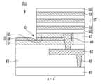
도 12a 및 도 12b를 참조하면, 베이스(70) 상에 인터커넥션 구조 및 층간절연막(73)을 형성한다. 베이스(70)는 기판, 주변 회로 등을 포함할 수 있다. 인터커넥션 구조는 제1 콘택 플러그(71), 배선(72) 등을 포함할 수 있다. 인터커넥션 구조는 층간절연막(73) 내에 형성될 수 있고, 베이스(70)와 전기적으로 연결될 수 있다. 예를 들어, 제1 콘택 플러그(71)가 주변 회로, 기판 등과 전기적으로 연결될 수 있다. 층간절연막(73)은 단일막 또는 다층막일 수 있다.Referring to FIGS. 12A and 12B, an interconnection structure and an interlayer insulating film (73) are formed on a base (70). The base (70) may include a substrate, peripheral circuits, etc. The interconnection structure may include a first contact plug (71), a wiring (72), etc. The interconnection structure may be formed within the interlayer insulating film (73) and may be electrically connected to the base (70). For example, the first contact plug (71) may be electrically connected to the peripheral circuits, the substrate, etc. The interlayer insulating film (73) may be a single film or a multilayer film.
이어서, 층간절연막(73) 상에 소스 구조(S)를 형성한다. 소스 구조(S)는 제1 소스막(74), 제2 소스막(75) 또는 희생막(76) 중 적어도 하나를 포함할 수 있다. 이어서, 소스 구조(S)를 관통하는 분리막들(77)을 형성한다. 분리막들(77)은 제2 방향(Ⅱ)으로 이격되어 위치될 수 있고, 제1 방향(I)으로 확장될 수 있다. 분리막(77)은 산화물, 질화물 등의 절연 물질을 포함할 수 있다.Next, a source structure (S) is formed on an interlayer insulating film (73). The source structure (S) may include at least one of a first source film (74), a second source film (75), or a sacrificial film (76). Next, separators (77) penetrating the source structure (S) are formed. The separators (77) may be positioned spaced apart from each other in the second direction (II) and may extend in the first direction (I). The separators (77) may include an insulating material such as an oxide or a nitride.
이어서, 소스 구조(S)를 관통하는 제2 콘택 플러그(78)를 형성한다. 제2 콘택 플러그(78)는 배선(72)과 연결된다. 소스 구조(S)는 제2 콘택 플러그(78), 배선(72) 및 제1 콘택 플러그(71)를 통해 기판(70) 또는 주변 회로와 전기적으로 연결될 수 있다.Next, a second contact plug (78) penetrating the source structure (S) is formed. The second contact plug (78) is connected to the wiring (72). The source structure (S) can be electrically connected to the substrate (70) or a peripheral circuit through the second contact plug (78), the wiring (72), and the first contact plug (71).
이어서, 소스 구조(S) 및 분리막(77) 상에 적층물(ST)을 형성한다. 적층물(ST)은 교대로 적층된 제1 물질막들(81) 및 제2 물질막들(82)을 포함할 수 있다. 제1 물질막들(81)은 제2 물질막들(82)에 대해 식각 선택비가 큰 물질을 포함할 수 있다.Next, a stack (ST) is formed on the source structure (S) and the separator (77). The stack (ST) may include first material films (81) and second material films (82) that are alternately stacked. The first material films (81) may include a material having a high etching selectivity with respect to the second material films (82).
이어서, 적층물(ST)을 관통하는 제1 슬릿(SL1) 또는 제2 슬릿(SL2)을 형성한다. 제2 슬릿(SL2)은 소스 구조(S)를 노출시키는 깊이를 가질 수 있다. 희생막(76)을 노출시키는 깊이를 타겟 깊이로 식각 공정을 수행하여, 제2 슬릿(SL2)을 형성할 수 있다 제2 슬릿(SL2)을 형성할 때, 일부 영역에 그루브(G)가 형성될 수 있고, 그루브(G)에 의해 제1 소스막(S1)이 노출될 수 있다.Next, a first slit (SL1) or a second slit (SL2) penetrating the stack (ST) is formed. The second slit (SL2) may have a depth that exposes the source structure (S). The second slit (SL2) may be formed by performing an etching process at a target depth that exposes the sacrificial film (76). When forming the second slit (SL2), a groove (G) may be formed in some area, and the first source film (S1) may be exposed by the groove (G).
제1 슬릿(SL1)은 제2 콘택 플러그(78)와 제1 방향(I)으로 이격될 수 있다. 제2 슬릿(SL2)은 제2 콘택 플러그(78)와 제2 방향(Ⅱ)으로 이웃할 수 있다. 제2 방향(Ⅱ)으로 이웃한 제2 슬릿들(SL2)의 사이에 제2 콘택 플러그(78)가 위치될 수 있다.The first slit (SL1) may be spaced apart from the second contact plug (78) in the first direction (I). The second slit (SL2) may be adjacent to the second contact plug (78) in the second direction (II). The second contact plug (78) may be positioned between the second slits (SL2) adjacent to each other in the second direction (II).
제1 방향(I) 및 제2 방향(Ⅱ)으로 정의된 평면에서, 제1 슬릿(SL1)과 제2 슬릿 (SL2)은 제2 방향(Ⅱ)으로 제1 거리(D1) 이격될 수 있다. 상기 평면에서, 분리막(77)의 엣지와 제2 콘택 플러그(78)는 제3 거리(D3) 이격될 수 있다. 제3 거리(D3)는 분리막(77)의 엣지로부터 제2 콘택 플러그(78)의 엣지까지의 거리일 수 있다. 여기서, 제3 거리(D3)는 제1 거리(D1)에 비해 큰 값을 가질 수 있다. 제3 거리(D3)는 제1 거리(D1)의 2배 이상일 수 있다.In a plane defined by a first direction (I) and a second direction (II), the first slit (SL1) and the second slit (SL2) can be spaced apart from each other by a first distance (D1) in the second direction (II). In the plane, the edge of the separator (77) and the second contact plug (78) can be spaced apart from each other by a third distance (D3). The third distance (D3) can be a distance from the edge of the separator (77) to the edge of the second contact plug (78). Here, the third distance (D3) can have a larger value than the first distance (D1). The third distance (D3) can be twice or more the first distance (D1).
도 12a 및 도 12c를 참조하면, 제1 슬릿(SL1) 또는 제2 슬릿(SL2)의 내벽에 보호막(86)을 형성할 수 있다. 이어서, 제1 슬릿(SL1) 또는 제2 슬릿(SL2)을 통해 희생막(76)을 선택적으로 식각하여 제1 개구부(OP1”)를 형성한다. 이때, 그루브(G)에 의해 노출된 제1 소스막(74)이 함께 식각될 수 있다. 따라서, 제1 개구부(OP1”)를 통해 층간절연막(73) 또는 분리막(77)이 노출될 수 있다.Referring to FIGS. 12A and 12C, a protective film (86) may be formed on the inner wall of the first slit (SL1) or the second slit (SL2). Subsequently, the sacrificial film (76) is selectively etched through the first slit (SL1) or the second slit (SL2) to form a first opening (OP1”). At this time, the first source film (74) exposed by the groove (G) may be etched together. Accordingly, the interlayer insulating film (73) or the separator (77) may be exposed through the first opening (OP1”).
제1 개구부(OP1”)를 형성할 때, 제2 슬릿(SL2)을 통해 식각 조성물이 유입되어 희생막(76)을 식각할 수 있다. 그런데, 제2 콘택 플러그(78)와 제2 슬릿(SL2)이 인접한 영역에 분리막(77)이 존재한다. 따라서, 분리막(77)에 의해 식각 조성물이 제2 슬릿(SL2)으로부터 제2 콘택 플러그(78)로 도달하는 최단 거리를 증가시킬 수 있다. 또한, 분리막(77)의 엣지와 제2 콘택 플러그(78)가 충분한 거리, 예를 들어, 제3 거리(D3) 이격되어 있으므로, 제2 콘택 플러그(78) 주변의 희생막(76)이 식각되는 것을 방지할 수 있다. 따라서, 희생막(76)을 식각하는 과정에서 제2 콘택 플러그(78)가 노출되는 것을 방지할 수 있다.When forming the first opening (OP1”), an etching composition can be introduced through the second slit (SL2) to etch the sacrificial film (76). However, a separator (77) exists in an area where the second contact plug (78) and the second slit (SL2) are adjacent. Therefore, the shortest distance for the etching composition to reach the second contact plug (78) from the second slit (SL2) can be increased by the separator (77). In addition, since the edge of the separator (77) and the second contact plug (78) are spaced apart from each other by a sufficient distance, for example, a third distance (D3), the sacrificial film (76) around the second contact plug (78) can be prevented from being etched. Therefore, the second contact plug (78) can be prevented from being exposed during the process of etching the sacrificial film (76).
이어서, 앞서 도 7c를 참조하여 설명한 바와 같이, 제1 개구부(OP1)를 통해 노출된 제1 메모리막(53)을 식각한다. 이를 통해 채널막이 노출될 수 있다.Next, as described above with reference to Fig. 7c, the first memory film (53) exposed through the first opening (OP1) is etched. Through this, the channel film can be exposed.
도 12a 및 도 12d를 참조하면, 도전막(87)을 형성한다. 도전막(87)은 제1 개구부(OP1”) 및 제2 슬릿(SL2)내에 형성될 수 있다. 도전막(87)은 제1 개구부(OP1”) 및 제1 슬릿(SL1)을 완전히 채우지 않는 두께로 형성될 수 있다. 도전막(57')은 제1 개구부(OP1”) 내에 위치된 제1 캐비티(C1)를 포함할 수 있다. 도전막(87)은 폴리실리콘, 금속 등의 도전 물질을 포함할 수 있다.Referring to FIGS. 12A and 12D, a conductive film (87) is formed. The conductive film (87) may be formed within the first opening (OP1”) and the second slit (SL2). The conductive film (87) may be formed with a thickness that does not completely fill the first opening (OP1”) and the first slit (SL1). The conductive film (57') may include a first cavity (C1) positioned within the first opening (OP1”). The conductive film (87) may include a conductive material such as polysilicon or a metal.
도 12a 및 도 12e를 참조하면, 제2 슬릿(SL2) 내에 형성된 도전막(87)을 식각한다. 식각 과정에서 제1 캐비티(C1)를 통해 유입된 식각 조성물에 의해, 제1 캐비티(C1) 주변의 식각 속도가 증가될 수 있다. 따라서, 제1 캐비티(C1) 주변의 도전막(87)이 제거될 수 있고, 소스 구조(S) 내에 제2 캐비티(C2)가 형성될 수 있다. 제2 캐비티(C2)는 분리막(77)을 노출시킬 수 있고, 제2 콘택 플러그(78)까지 확장되지 않는다. 따라서, 제2 콘택 플러그(78)가 제2 캐비티 (C2)에 의해 노출되지 않는다. 이어서, 보호막(86)을 제거할 수 있다.Referring to FIGS. 12A and 12E, a conductive film (87) formed within the second slit (SL2) is etched. During the etching process, an etching speed around the first cavity (C1) may be increased by an etching composition introduced through the first cavity (C1). Accordingly, the conductive film (87) around the first cavity (C1) may be removed, and a second cavity (C2) may be formed within the source structure (S). The second cavity (C2) may expose the separator (77) and may not extend to the second contact plug (78). Accordingly, the second contact plug (78) is not exposed by the second cavity (C2). Subsequently, the protective film (86) may be removed.
도 12a 및 도 12f를 참조하면, 제1 물질막들(81)을 도전막들(89)로 대체한다. 도전막들(89)을 형성하기 전에, 제2 메모리막들(88)을 추가로 형성할 수 있다. 제2 메모리막들(88) 각각은 터널절연막, 데이터 저장막 또는 전하차단막 중 적어도 하나를 포함할 수 있다. 여기서, 전하차단막은 알루미늄산화물(Al2O3)을 포함할 수 있다. 또한, 제2 개구부들(OP2) 내에 전하차단막을 형성한 후에 열처리 공정을 수행할 수 있다. 제2 캐비티(C2)에 의해 제2 콘택 플러그(78)가 노출되지 않으므로, 열처리 공정을 수행하더라도 제2 콘택 플러그(78)가 산화되거나 손상되지 않는다.Referring to FIGS. 12A and 12F, the first material films (81) are replaced with conductive films (89). Before forming the conductive films (89), second memory films (88) may be additionally formed. Each of the second memory films (88) may include at least one of a tunnel insulating film, a data storage film, or a charge blocking film. Here, the charge blocking film may include aluminum oxide (Al2 O3 ). In addition, a heat treatment process may be performed after forming the charge blocking film in the second openings (OP2). Since the second contact plug (78) is not exposed by the second cavity (C2), even if the heat treatment process is performed, the second contact plug (78) is not oxidized or damaged.
이어서, 제2 슬릿(SL2) 내에 제2 슬릿 구조(92)를 형성한다. 제2 슬릿(SL2) 내에 절연 물질을 채워 제2 슬릿 구조(92)를 형성할 수 있다. 또는, 제2 슬릿(SL2)의 측벽에 절연 스페이서(92A)를 형성한 후, 제2 슬릿(SL2) 내에 도전 물질을 채워 소스 구조(S)와 전기적으로 연결된 소스 콘택 구조(92B) 를 형성함으로써, 제2 슬릿 구조(92)를 형성할 수 있다. 제2 슬릿 구조(92)는 재2 캐비티(C2) 내에 형성될 수 있고, 분리막(77)과 접할 수 있다.Next, a second slit structure (92) is formed within the second slit (SL2). The second slit structure (92) may be formed by filling an insulating material within the second slit (SL2). Alternatively, the second slit structure (92) may be formed by forming an insulating spacer (92A) on a sidewall of the second slit (SL2) and then filling a conductive material within the second slit (SL2) to form a source contact structure (92B) electrically connected to the source structure (S). The second slit structure (92) may be formed within the second cavity (C2) and may be in contact with the separator (77).
전술한 바와 같은 제조 방법에 따르면, 제2 슬릿(SL2) 형성 과정에서 그루브(G)가 형성될 수 있고, 그로 인해 소스 구조(S)가 제2 캐비티(C2)를 포함할 수 있다. 그러나, 분리막(77)에 의해 제2 캐비티(C2)와 제2 콘택 플러그(78)가 이격되므로, 제조 과정에서 제2 콘택 플러그(78)가 손상되는 것을 방지할 수 있다.According to the manufacturing method described above, a groove (G) can be formed during the process of forming the second slit (SL2), and thus the source structure (S) can include the second cavity (C2). However, since the second cavity (C2) and the second contact plug (78) are separated by the separator (77), the second contact plug (78) can be prevented from being damaged during the manufacturing process.
도 13은 본 발명의 일 실시예에 따른 메모리 시스템의 구성을 나타낸 블록도이다.Figure 13 is a block diagram showing the configuration of a memory system according to one embodiment of the present invention.
도 13을 참조하면, 본 발명의 일 실시예에 따른 메모리 시스템(1000)은 메모리 장치(1200)와 컨트롤러(1100)를 포함한다.Referring to FIG. 13, a memory system (1000) according to one embodiment of the present invention includes a memory device (1200) and a controller (1100).
메모리 장치(1200)는 텍스트, 그래픽, 소프트웨어 코드 등과 같은 다양한 데이터 형태를 갖는 데이터 정보를 저장하는데 사용된다. 메모리 장치(1200)는 비휘발성 메모리일 수 있다. 또한, 메모리 장치는(1200)는 앞서 도 1a 내지 도 12f를 참조하여 설명한 구조를 가질 수 있고, 앞서 도 1a 내지 도 12f를 참조하여 설명한 제조 방법에 따라 제조될 수 있다. 실시예로서, 메모리 장치(1200)는 하부 배선; 상기 하부 배선 상의 소스 구조; 상기 소스 구조 상의 적층물; 상기 적층물을 관통하는 제1 슬릿 구조; 상기 적층물을 관통하는 제2 슬릿 구조; 상기 제1 슬릿 구조와 제1 방향으로 이웃하고, 상기 소스 구조를 관통하고 상기 하부 배선과 전기적으로 연결된 콘택 플러그를 포함할 수 있고, 상기 제1 슬릿 구조와 상기 제2 슬릿 구조는 상기 제1 방향과 교차된 제2 방향으로 제1 거리 이격되고, 상기 제1 슬릿 구조와 상기 콘택 플러그는 상기 제1 방향으로 제2 거리 이격되고, 상기 제2 거리는 상기 제1 거리에 비해 클 수 있다. 메모리 장치(1200)의 구조 및 제조 방법은 앞서 설명한 바와 동일하므로, 구체적인 설명은 생략하도록 한다.The memory device (1200) is used to store data information having various data forms such as text, graphics, software codes, etc. The memory device (1200) may be a nonvolatile memory. In addition, the memory device (1200) may have a structure described above with reference to FIGS. 1A to 12F, and may be manufactured according to the manufacturing method described above with reference to FIGS. 1A to 12F. As an embodiment, the memory device (1200) includes: a lower wiring; a source structure on the lower wiring; a stacked structure on the source structure; a first slit structure penetrating the stacked structure; a second slit structure penetrating the stacked structure; The first slit structure may include a contact plug adjacent to the first direction, penetrating the source structure, and electrically connected to the lower wiring, wherein the first slit structure and the second slit structure are spaced apart from each other by a first distance in a second direction intersecting the first direction, and the first slit structure and the contact plug are spaced apart from each other by a second distance in the first direction, and the second distance may be greater than the first distance. Since the structure and the manufacturing method of the memory device (1200) are the same as those described above, a detailed description thereof will be omitted.
컨트롤러(1100)는 호스트 및 메모리 장치(1200)에 연결되며, 호스트로부터의 요청에 응답하여 메모리 장치(1200)를 액세스하도록 구성된다. 예를 들면, 컨트롤러(1100)는 메모리 장치(1200)의 읽기, 쓰기, 소거, 배경(background) 동작 등을 제어하도록 구성된다.The controller (1100) is connected to the host and the memory device (1200), and is configured to access the memory device (1200) in response to a request from the host. For example, the controller (1100) is configured to control reading, writing, erasing, background operations, etc. of the memory device (1200).
컨트롤러(1100)는 RAM(Random Access Memory; 1110), CPU(Central Processing Unit; 1120), 호스트 인터페이스(Host Interface; 1130), ECC 회로(Error Correction Code Circuit; 1140), 메모리 인터페이스(Memory Interface; 1150) 등을 포함한다.The controller (1100) includes a RAM (Random Access Memory; 1110), a CPU (Central Processing Unit; 1120), a host interface (Host Interface; 1130), an ECC circuit (Error Correction Code Circuit; 1140), a memory interface (Memory Interface; 1150), etc.
여기서, RAM(1110)은 CPU(1120) 의 동작 메모리, 메모리 장치(1200)와 호스트 간의 캐시 메모리, 메모리 장치(1200)와 호스트 간의 버퍼 메모리 등으로 사용될 수 있다. 참고로, RAM(1110)은 SRAM(Static Random Access Memory), ROM(Read Only Memory) 등으로 대체될 수 있다.Here, RAM (1110) can be used as an operating memory of CPU (1120), a cache memory between the memory device (1200) and the host, a buffer memory between the memory device (1200) and the host, etc. For reference, RAM (1110) can be replaced with SRAM (Static Random Access Memory), ROM (Read Only Memory), etc.
CPU(1120)는 컨트롤러(1100)의 전반적인 동작을 제어하도록 구성된다. 예를 들어, CPU(1120)는 RAM(1110)에 저장된 플래시 변환 계층(Flash Translation Layer; FTL)과 같은 펌웨어를 운용하도록 구성된다.The CPU (1120) is configured to control the overall operation of the controller (1100). For example, the CPU (1120) is configured to operate firmware such as a flash translation layer (FTL) stored in the RAM (1110).
호스트 인터페이스(1130)는 호스트와의 인터페이싱을 수행하도록 구성된다. 예를 들어, 컨트롤러(1100)는 USB(Universal Serial Bus)프로토콜, MMC(MultiMedia Card) 프로토콜, PCI(Peripheral Component Interconnection)프로토콜, PCI-E(PCI-Express) 프로토콜, ATA(Advanced Technology Attachment) 프로토콜, Serial-ATA 프로토콜, Parallel-ATA 프로토콜, SCSI(Small Computer Small Interface) 프로토콜, ESDI(Enhanced Small Disk Interface) 프로토콜, 그리고 IDE(Integrated Drive Electronics) 프로토콜, 프라이빗(private) 프로토콜 등과 같은 다양한 인터페이스 프로토콜들 중 적어도 하나를 통해 호스트와 통신한다.The host interface (1130) is configured to perform interfacing with the host. For example, the controller (1100) communicates with the host through at least one of various interface protocols, such as a Universal Serial Bus (USB) protocol, a MultiMedia Card (MMC) protocol, a Peripheral Component Interconnection (PCI) protocol, a PCI-E (PCI-Express) protocol, an Advanced Technology Attachment (ATA) protocol, a Serial-ATA protocol, a Parallel-ATA protocol, a Small Computer Small Interface (SCSI) protocol, an Enhanced Small Disk Interface (ESDI) protocol, an Integrated Drive Electronics (IDE) protocol, a private protocol, etc.
ECC 회로(1140)는 오류 정정 코드(ECC)를 이용하여 메모리 장치(1200)로부터 리드된 데이터에 포함된 오류를 검출하고, 정정하도록 구성된다.The ECC circuit (1140) is configured to detect and correct errors included in data read from a memory device (1200) using an error correction code (ECC).
메모리 인터페이스(1150)는 메모리 장치(1200)와의 인터페이싱을 수행하도록 구성된다. 예를 들어, 메모리 인터페이스(1150)는 낸드 인터페이스 또는 노어 인터페이스를 포함한다.The memory interface (1150) is configured to interface with the memory device (1200). For example, the memory interface (1150) includes a NAND interface or a NOR interface.
참고로, 컨트롤러(1100)는 데이터를 임시 저장하기 위한 버퍼 메모리(미도시됨)를 더 포함할 수 있다. 여기서, 버퍼 메모리는 호스트 인터페이스(1130)를 통해 외부로 전달되는 데이터를 임시 저장하거나, 메모리 인터페이스(1150)를 통해 메모리 장치(1200)로부터 전달되는 데이터를 임시로 저장하는데 사용될 수 있다. 또한, 컨트롤러(1100)는 호스트와의 인터페이싱을 위한 코드 데이터를 저장하는 ROM을 더 포함할 수 있다.For reference, the controller (1100) may further include a buffer memory (not shown) for temporarily storing data. Here, the buffer memory may be used to temporarily store data transmitted externally through the host interface (1130) or to temporarily store data transmitted from the memory device (1200) through the memory interface (1150). In addition, the controller (1100) may further include a ROM for storing code data for interfacing with the host.
이와 같이, 본 발명의 일 실시예에 따른 메모리 시스템(1000)은 집적도가 향상되고 특성이 개선된 메모리 장치(1200)를 포함하므로, 메모리 시스템(1000)의 집적도 및 특성 또한 향상시킬 수 있다.In this way, since the memory system (1000) according to one embodiment of the present invention includes a memory device (1200) with improved integration and characteristics, the integration and characteristics of the memory system (1000) can also be improved.
도 14는 본 발명의 일 실시예에 따른 메모리 시스템의 구성을 나타낸 블록도이다. 이하, 앞서 설명된 내용과 중복된 내용은 생략하여 설명하도록 한다.Figure 14 is a block diagram showing the configuration of a memory system according to one embodiment of the present invention. Hereinafter, any duplicate content described above will be omitted for explanation.
도 14를 참조하면, 본 발명의 일 실시예에 따른 메모리 시스템(1000')은 메모리 장치(1200')와 컨트롤러(1100)를 포함한다. 또한, 컨트롤러(1100)는 RAM(1110), CPU(1120), 호스트 인터페이스(1130), ECC 회로(1140), 메모리 인터페이스(1150) 등을 포함한다.Referring to FIG. 14, a memory system (1000') according to one embodiment of the present invention includes a memory device (1200') and a controller (1100). In addition, the controller (1100) includes a RAM (1110), a CPU (1120), a host interface (1130), an ECC circuit (1140), a memory interface (1150), etc.
메모리 장치(1200')는 비휘발성 메모리일 수 있다. 또한, 메모리 장치(1200')는 앞서 도 1a 내지 도 12f를 참조하여 설명한 구조를 가질 수 있고, 앞서 도 1a 내지 도 12f를 참조하여 설명한 제조 방법에 따라 제조될 수 있다. 실시예로서, 메모리 장치(1200')는 하부 배선; 상기 하부 배선 상의 소스 구조; 상기 소스 구조 상의 적층물; 상기 적층물을 관통하는 제1 슬릿 구조; 상기 적층물을 관통하는 제2 슬릿 구조; 상기 제1 슬릿 구조와 제1 방향으로 이웃하고, 상기 소스 구조를 관통하고 상기 하부 배선과 전기적으로 연결된 콘택 플러그를 포함할 수 있고, 상기 제1 슬릿 구조와 상기 제2 슬릿 구조는 상기 제1 방향과 교차된 제2 방향으로 제1 거리 이격되고, 상기 제1 슬릿 구조와 상기 콘택 플러그는 상기 제1 방향으로 제2 거리 이격되고, 상기 제2 거리는 상기 제1 거리에 비해 클 수 있다. 메모리 장치(1200')의 구조 및 제조 방법은 앞서 설명한 바와 동일하므로, 구체적인 설명은 생략하도록 한다.The memory device (1200') may be a nonvolatile memory. In addition, the memory device (1200') may have a structure described above with reference to FIGS. 1A to 12F, and may be manufactured according to a manufacturing method described above with reference to FIGS. 1A to 12F. As an embodiment, the memory device (1200') may include: a lower wiring; a source structure on the lower wiring; a stacked structure on the source structure; a first slit structure penetrating the stacked structure; a second slit structure penetrating the stacked structure; and a contact plug adjacent to the first slit structure in a first direction, penetrating the source structure, and electrically connected to the lower wiring, wherein the first slit structure and the second slit structure are spaced apart from each other by a first distance in a second direction intersecting the first direction, and the first slit structure and the contact plug are spaced apart from each other by a second distance in the first direction, and the second distance may be greater than the first distance. Since the structure and manufacturing method of the memory device (1200') are the same as described above, a detailed description will be omitted.
또한, 메모리 장치(1200')는 복수의 메모리 칩들로 구성된 멀티-칩 패키지일 수 있다. 복수의 메모리 칩들은 복수의 그룹들로 분할되며, 복수의 그룹들은 제 1 내지 제 k 채널들(CH1~CHk)을 통해 컨트롤러(1100)와 통신하도록 구성된다. 또한, 하나의 그룹에 속한 메모리 칩들은 공통 채널을 통해 컨트롤러(1100)와 통신하도록 구성된다. 참고로, 하나의 채널에 하나의 메모리 칩이 연결되도록 메모리 시스템(1000')이 변형되는 것도 가능하다.In addition, the memory device (1200') may be a multi-chip package composed of a plurality of memory chips. The plurality of memory chips are divided into a plurality of groups, and the plurality of groups are configured to communicate with the controller (1100) through the first to kth channels (CH1 to CHk). In addition, the memory chips belonging to one group are configured to communicate with the controller (1100) through a common channel. For reference, the memory system (1000') may also be modified so that one memory chip is connected to one channel.
이와 같이, 본 발명의 일 실시예에 따른 메모리 시스템(1000')은 집적도가 향상되고 특성이 개선된 메모리 장치(1200')를 포함하므로, 메모리 시스템(1000')의 집적도 및 특성 또한 향상시킬 수 있다. 특히, 메모리 장치(1200')를 멀티-칩 패키지로 구성함으로써, 메모리 시스템(1000')의 데이터 저장 용량을 증가시키고, 구동 속도를 향상시킬 수 있다.In this way, since the memory system (1000') according to one embodiment of the present invention includes a memory device (1200') with improved integration and characteristics, the integration and characteristics of the memory system (1000') can also be improved. In particular, by configuring the memory device (1200') as a multi-chip package, the data storage capacity of the memory system (1000') can be increased and the operating speed can be improved.
도 15는 본 발명의 일 실시예에 따른 컴퓨팅 시스템의 구성을 나타내는 블록도이다. 이하, 앞서 설명된 내용과 중복된 내용은 생략하여 설명하도록 한다.Figure 15 is a block diagram showing the configuration of a computing system according to one embodiment of the present invention. Hereinafter, any duplicate content described above will be omitted for explanation.
도 15를 참조하면, 본 발명의 일 실시예에 따른 컴퓨팅 시스템(2000)은 메모리 장치(2100), CPU(2200), RAM(2300), 유저 인터페이스(2400), 전원(2500), 시스템 버스(2600) 등을 포함한다.Referring to FIG. 15, a computing system (2000) according to one embodiment of the present invention includes a memory device (2100), a CPU (2200), a RAM (2300), a user interface (2400), a power source (2500), a system bus (2600), etc.
메모리 장치(2100)는 유저 인터페이스(2400)를 통해 제공된 데이터, CPU(2200)에 의해 처리된 데이터 등을 저장한다. 또한, 메모리 장치(2100)은 시스템 버스(2600)를 통해 CPU(2200), RAM(2300), 유저 인터페이스(2400), 전원(2500) 등에 전기적으로 연결된다. 예를 들어, 메모리 장치(2100)는 컨트롤러(미도시됨)를 통해 시스템 버스(2600)에 연결되거나, 시스템 버스(2600)에 직접 연결될 수 있다. 메모리 장치(2100)가 시스템 버스(2600)에 직접 연결되는 경우, 컨트롤러의 기능은 CPU(2200), RAM(2300) 등에 의해 수행될 수 있다.The memory device (2100) stores data provided through the user interface (2400), data processed by the CPU (2200), etc. In addition, the memory device (2100) is electrically connected to the CPU (2200), the RAM (2300), the user interface (2400), the power supply (2500), etc. via the system bus (2600). For example, the memory device (2100) may be connected to the system bus (2600) via a controller (not shown) or may be directly connected to the system bus (2600). When the memory device (2100) is directly connected to the system bus (2600), the function of the controller may be performed by the CPU (2200), the RAM (2300), etc.
여기서, 메모리 장치(2100)는 비휘발성 메모리 일 수 있다. 또한, 메모리 장치(2100)는 앞서 도 1a 내지 도 12f를 참조하여 설명한 구조를 가질 수 있고, 앞서 도 1a 내지 도 12f를 참조하여 설명한 제조 방법에 따라 제조될 수 있다. 실시예로서, 메모리 장치(2100)는 하부 배선; 상기 하부 배선 상의 소스 구조; 상기 소스 구조 상의 적층물; 상기 적층물을 관통하는 제1 슬릿 구조; 상기 적층물을 관통하는 제2 슬릿 구조; 상기 제1 슬릿 구조와 제1 방향으로 이웃하고, 상기 소스 구조를 관통하고 상기 하부 배선과 전기적으로 연결된 콘택 플러그를 포함할 수 있고, 상기 제1 슬릿 구조와 상기 제2 슬릿 구조는 상기 제1 방향과 교차된 제2 방향으로 제1 거리 이격되고, 상기 제1 슬릿 구조와 상기 콘택 플러그는 상기 제1 방향으로 제2 거리 이격되고, 상기 제2 거리는 상기 제1 거리에 비해 클 수 있다. 메모리 장치(2100)의 구조 및 제조 방법은 앞서 설명한 바와 동일하므로, 구체적인 설명은 생략하도록 한다.Here, the memory device (2100) may be a nonvolatile memory. In addition, the memory device (2100) may have the structure described with reference to FIGS. 1A to 12F above, and may be manufactured according to the manufacturing method described with reference to FIGS. 1A to 12F above. As an embodiment, the memory device (2100) may include: a lower wiring; a source structure on the lower wiring; a stacked structure on the source structure; a first slit structure penetrating the stacked structure; a second slit structure penetrating the stacked structure; and a contact plug adjacent to the first slit structure in a first direction, penetrating the source structure, and electrically connected to the lower wiring, wherein the first slit structure and the second slit structure are spaced apart from each other by a first distance in a second direction intersecting the first direction, and the first slit structure and the contact plug are spaced apart from each other by a second distance in the first direction, and the second distance may be greater than the first distance. Since the structure and manufacturing method of the memory device (2100) are the same as described above, a detailed description will be omitted.
또한, 메모리 장치(2100)은 도 5를 참조하여 설명한 바와 같이 복수의 메모리 칩들로 구성된 멀티-칩 패키지일 수 있다.Additionally, the memory device (2100) may be a multi-chip package composed of a plurality of memory chips as described with reference to FIG. 5.
이와 같은 구성을 갖는 컴퓨팅 시스템(2000)은 컴퓨터, UMPC (Ultra Mobile PC), 워크스테이션, 넷북(net-book), PDA (Personal Digital Assistants), 포터블 컴퓨터(portable computer), 웹 타블렛(web tablet), 무선 전화기(wireless phone), 모바일 폰(mobile phone), 스마트폰(smart phone), e-북(e-book), PMP(Portable MultimediaPlayer), 휴대용 게임기, 네비게이션(navigation) 장치, 블랙박스(black box), 디지털 카메라(digital camera), 3차원 수상기(3-dimensional television), 디지털 음성 녹음기(digital audiorecorder), 디지털 음성 재생기(digital audioplayer), 디지털 영상 녹화기(digital picture recorder), 디지털 영상 재생기(digital picture player), 디지털 동영상 녹화기(digital video recorder), 디지털 동영상 재생기(digital video player), 정보를 무선 환경에서 송수신할 수 있는 장치, 홈 네트워크를 구성하는 다양한 전자 장치들 중 하나, 컴퓨터 네트워크를 구성하는 다양한 전자 장치들 중 하나, 텔레매틱스 네트워크를 구성하는 다양한 전자 장치들 중 하나, RFID 장치 등일 수 있다.A computing system (2000) having such a configuration may be a computer, an Ultra Mobile PC (UMPC), a workstation, a net-book, a PDA (Personal Digital Assistants), a portable computer, a web tablet, a wireless phone, a mobile phone, a smart phone, an e-book, a Portable MultimediaPlayer (PMP), a portable game console, a navigation device, a black box, a digital camera, a 3-dimensional television, a digital audiorecorder, a digital audioplayer, a digital picture recorder, a digital picture player, a digital video recorder, a digital video player, a device capable of transmitting and receiving information in a wireless environment, one of various electronic devices forming a home network, one of various electronic devices forming a computer network, one of various electronic devices forming a telematics network. It could be one of many electronic devices, such as an RFID device.
이와 같이, 본 발명의 일 실시예에 따른 컴퓨팅 시스템(2000)은 집적도가 향상되고 특성이 개선된 메모리 장치(2100)를 포함하므로, 컴퓨팅 시스템(2000)의 특성 또한 향상시킬 수 있다.In this way, since the computing system (2000) according to one embodiment of the present invention includes a memory device (2100) with improved integration and characteristics, the characteristics of the computing system (2000) can also be improved.
도 16은 본 발명의 일 실시예에 따른 컴퓨팅 시스템을 나타내는 블록도이다.FIG. 16 is a block diagram illustrating a computing system according to one embodiment of the present invention.
도 16을 참조하면, 본 발명의 일 실시예에 따른 컴퓨팅 시스템(3000)은 운영 체제(3200), 어플리케이션(3100), 파일 시스템(3300), 변환 계층(3400) 등을 포함하는 소프트웨어 계층을 포함한다. 또한, 컴퓨팅 시스템(3000)은 메모리 장치(3500) 등의 하드웨어 계층을 포함한다.Referring to FIG. 16, a computing system (3000) according to one embodiment of the present invention includes a software layer including an operating system (3200), an application (3100), a file system (3300), a conversion layer (3400), etc. In addition, the computing system (3000) includes a hardware layer such as a memory device (3500).
운영 체제(3200)는 컴퓨팅 시스템(3000)의 소프트웨어, 하드웨어 자원 등을 관리하기 위한 것으로, 중앙처리장치의 프로그램 실행을 제어할 수 있다. 어플리케이션(3100)은 컴퓨팅 시스템(3000)에서 실시되는 다양한 응용 프로그램으로, 운영 체제(3200)에 의해 실행되는 유틸리티일 수 있다.The operating system (3200) is for managing software, hardware resources, etc. of the computing system (3000) and can control the execution of programs of the central processing unit. The application (3100) is a variety of application programs implemented in the computing system (3000) and may be a utility executed by the operating system (3200).
파일 시스템(3300)은 컴퓨팅 시스템(3000)에 존재하는 데이터, 파일 등을 관리하기 위한 논리적인 구조를 의미하며, 규칙에 따라 메모리 장치(3500) 등에 저장할 파일 또는 데이터를 조직화한다. 파일 시스템(3300)은 컴퓨팅 시스템(3000)에서 사용되는 운영 체제(3200)에 따라 결정될 수 있다. 예를 들어, 운영 체제(3200)가 마이크로소프트(Microsoft)사의 윈도우즈(Windows) 계열인 경우, 파일 시스템(3300)은 FAT(File Allocation Table), NTFS(NT file system) 등일 수 있다. 또한, 운영 체제(3200)가 유닉스/리눅스(Unix/Linux) 계열인 경우, 파일 시스템(3300)은 EXT(extended file system), UFS(Unix File System), JFS(Journaling File System) 등일 수 있다.The file system (3300) refers to a logical structure for managing data, files, etc. existing in the computing system (3000), and organizes files or data to be stored in a memory device (3500), etc., according to rules. The file system (3300) may be determined according to the operating system (3200) used in the computing system (3000). For example, if the operating system (3200) is a Windows series from Microsoft, the file system (3300) may be a FAT (File Allocation Table), an NTFS (NT file system), etc. In addition, if the operating system (3200) is a Unix/Linux series, the file system (3300) may be an EXT (extended file system), a UFS (Unix File System), a JFS (Journaling File System), etc.
본 도면에서는 운영 체제(3200), 어플리케이션(3100) 및 파일 시스템(3300)을 별도의 블록으로 도시하였으나, 어플리케이션(3100) 및 파일 시스템(3300)은 운영 체제(3200) 내에 포함된 것일 수 있다.In this drawing, the operating system (3200), application (3100), and file system (3300) are depicted as separate blocks, but the application (3100) and file system (3300) may be included within the operating system (3200).
변환 계층(Translation Layer; 3400)은 파일 시스템(3300)으로부터의 요청에 응답하여 메모리 장치(3500)에 적합한 형태로 어드레스를 변환한다. 예를 들어, 변환 계층(3400)은 파일 시스템(3300)이 생성한 로직 어드레스를 메모리 장치(3500)의 피지컬 어드레스로 변환한다. 여기서, 로직 어드레스와 피지컬 어드레스의 맵핑 정보는 어드레스 변환 테이블(address translation table)로 저장될 수 있다. 예를 들어, 변환 계층(3400)은 플래시 변환 계층(Flash Translation Layer; FTL), 유니버설 플래시 스토리지 링크 계층(Universal Flash Storage Link Layer, ULL) 등일 수 있다.The translation layer (3400) translates an address into a form suitable for the memory device (3500) in response to a request from the file system (3300). For example, the translation layer (3400) translates a logical address generated by the file system (3300) into a physical address of the memory device (3500). Here, mapping information between the logical address and the physical address may be stored as an address translation table. For example, the translation layer (3400) may be a flash translation layer (FTL), a universal flash storage link layer (ULL), etc.
메모리 장치(3500)는 비휘발성 메모리 일 수 있다. 또한, 메모리 장치(3500)는 앞서 도 1a 내지 도 12f를 참조하여 설명한 구조를 가질 수 있고, 앞서 도 1a 내지 도 12f를 참조하여 설명한 제조 방법에 따라 제조될 수 있다. 실시예로서, 메모리 장치(3500)는 하부 배선; 상기 하부 배선 상의 소스 구조; 상기 소스 구조 상의 적층물; 상기 적층물을 관통하는 제1 슬릿 구조; 상기 적층물을 관통하는 제2 슬릿 구조; 상기 제1 슬릿 구조와 제1 방향으로 이웃하고, 상기 소스 구조를 관통하고 상기 하부 배선과 전기적으로 연결된 콘택 플러그를 포함할 수 있고, 상기 제1 슬릿 구조와 상기 제2 슬릿 구조는 상기 제1 방향과 교차된 제2 방향으로 제1 거리 이격되고, 상기 제1 슬릿 구조와 상기 콘택 플러그는 상기 제1 방향으로 제2 거리 이격되고, 상기 제2 거리는 상기 제1 거리에 비해 클 수 있다. 메모리 장치(3500)의 구조 및 제조 방법은 앞서 설명한 바와 동일하므로, 구체적인 설명은 생략하도록 한다.The memory device (3500) may be a nonvolatile memory. In addition, the memory device (3500) may have the structure described above with reference to FIGS. 1A to 12F, and may be manufactured according to the manufacturing method described above with reference to FIGS. 1A to 12F. As an embodiment, the memory device (3500) may include: a lower wiring; a source structure on the lower wiring; a stacked structure on the source structure; a first slit structure penetrating the stacked structure; a second slit structure penetrating the stacked structure; and a contact plug adjacent to the first slit structure in a first direction, penetrating the source structure, and electrically connected to the lower wiring, wherein the first slit structure and the second slit structure are spaced apart from each other by a first distance in a second direction intersecting the first direction, and the first slit structure and the contact plug are spaced apart from each other by a second distance in the first direction, and the second distance may be greater than the first distance. Since the structure and manufacturing method of the memory device (3500) are the same as described above, a detailed description will be omitted.
이러한 구성을 갖는 컴퓨팅 시스템(3000)은 상위 레벨 영역에서 수행되는 운영체제 계층과 하위 레벨 영역에서 수행되는 컨트롤러 계층으로 구분될 수 있다. 여기서, 어플리케이션(3100), 운영 체제(3200) 및 파일 시스템(3300)은 운영 체제 계층에 포함되며, 컴퓨팅 시스템(3000)의 동작 메모리에 의해 구동될 수 있다. 또한, 변환 계층(3400)은 운영 체제 계층에 포함되거나, 컨트롤러 계층에 포함될 수 있다.A computing system (3000) having such a configuration can be divided into an operating system layer performed in an upper level area and a controller layer performed in a lower level area. Here, an application (3100), an operating system (3200), and a file system (3300) are included in the operating system layer and can be driven by the operating memory of the computing system (3000). In addition, a conversion layer (3400) can be included in the operating system layer or the controller layer.
이와 같이, 본 발명의 일 실시예에 따른 컴퓨팅 시스템(3000)은 집적도가 향상되고 특성이 개선된 메모리 장치(3500)를 포함하므로, 컴퓨팅 시스템(3000)의 특성 또한 향상시킬 수 있다.In this way, since the computing system (3000) according to one embodiment of the present invention includes a memory device (3500) with improved integration and characteristics, the characteristics of the computing system (3000) can also be improved.
1: 게이트 절연막2: 게이트 전극
3: 정션4: 소자분리막
5: 층간 절연막10: 기판
11: 도전막12: 절연막
13: 메모리막15: 분리막
16: 제1 소스막17: 제2 소스막
18: 제3 소스막19: 희생막
40: 베이스41: 제1 콘택 플러그
42: 배선43: 층간절연막
44: 제1 소스막45: 제2 소스막
46: 희생막47: 분리막
48: 제2 콘택 플러그51: 제1 물질막
52: 제2 물질막53: 제1 메모리막
54: 채널막55: 갭필막
56: 보호막57, 57': 도전막
58: 제2 메모리막59: 도전막
61: 제1 슬릿 구조62: 제2 슬릿 구조
70: 베이스71: 제1 콘택 플러그
72: 배선73: 층간절연막
74: 제1 소스막75: 제2 소스막
76: 희생막77: 분리막
78: 제2 콘택 플러그81: 제1 물질막
82: 제2 물질막86: 보호막
87: 도전막88: 제2 메모리막
89: 도전막91: 제1 슬릿 구조
92: 제2 슬릿 구조S, S1, S1', S2, S2': 소스 구조
SL1: 제1 슬릿SLI1: 제1 슬릿 구조
SL2: 제2 슬릿SLI2: 제2 슬릿 구조
SLI3: 제3 슬릿 구조CP1: 제1 콘택 플러그
CP2: 제2 콘택 플러그UM: 배선
ST: 적층물CH: 채널 구조
TR: 트랜지스터1: Gate insulating film 2: Gate electrode
3: Junction 4: Device separation membrane
5: Interlayer insulation film 10: Substrate
11: Challenge film 12: Insulating film
13: Memory membrane 15: Separator membrane
16: First source curtain 17: Second source curtain
18: Third Source Curtain 19: Sacrifice Curtain
40: Base 41: First contact plug
42: Wiring 43: Interlayer insulation film
44: First source curtain 45: Second source curtain
46: Sacrificial membrane 47: Separator membrane
48: Second contact plug 51: First material film
52: Second material membrane 53: First memory membrane
54: Channel barrier 55: Gap barrier
56:
58: Second memory screen 59: Challenge screen
61: First slit structure 62: Second slit structure
70: Base 71: First contact plug
72: Wiring 73: Interlayer insulation film
74: First source curtain 75: Second source curtain
76: Sacrificial membrane 77: Separator membrane
78: Second contact plug 81: First material film
82: Second material film 86: Protective film
87: Challenge screen 88: 2nd memory screen
89: Challenge 91: First slit structure
92: Second slit structure S, S1, S1', S2, S2': Source structure
SL1: 1st slit SLI1: 1st slit structure
SL2: Second slit SLI2: Second slit structure
SLI3: Third slit structure CP1: First contact plug
CP2: 2nd contact plug UM: Wiring
ST: laminate CH: channel structure
TR: Transistor
Claims (33)
Translated fromKorean상기 배선 상의 소스 구조;
상기 소스 구조를 관통하여 상기 배선과 전기적으로 연결된 콘택 플러그;
상기 소스 구조 및 상기 콘택 플러그 상의 적층물;
상기 적층물을 관통하고, 상기 콘택 플러그와 제1 방향으로 이웃하는 제1 슬릿 구조; 및
상기 적층물을 관통하고, 상기 제1 슬릿 구조와 상기 제1 방향과 교차된 제2 방향으로 이웃한 제2 슬릿 구조
를 포함하고,
상기 제1 슬릿 구조와 상기 제2 슬릿 구조는 상기 제2 방향으로 제1 거리 이격되고, 상기 제1 슬릿 구조와 상기 콘택 플러그는 상기 제1 방향으로 제2 거리 이격되고, 상기 제2 거리는 상기 제1 거리에 비해 큰
반도체 장치.
wiring;
Source structure on the above wiring;
A contact plug electrically connected to the wiring by penetrating the source structure;
The above source structure and the laminate on the contact plug;
A first slit structure penetrating the above laminate and adjacent to the contact plug in the first direction; and
A second slit structure penetrating the above laminate and adjacent to the first slit structure in a second direction intersecting the first direction
Including,
The first slit structure and the second slit structure are spaced apart by a first distance in the second direction, and the first slit structure and the contact plug are spaced apart by a second distance in the first direction, and the second distance is greater than the first distance.
Semiconductor devices.
상기 제1 슬릿 구조는 상기 적층물을 관통하는 제1 관통부 및 상기 제1 관통부의 측벽으로부터 상기 소스 구조의 내부로 돌출된 제1 돌출부를 포함하는
반도체 장치.
In the first paragraph,
The first slit structure includes a first through-hole portion penetrating the laminate and a first protrusion portion protruding into the interior of the source structure from a sidewall of the first through-hole portion.
Semiconductor devices.
상기 콘택 플러그는 상기 제1 돌출부로부터 이격된
반도체 장치.
In the second paragraph,
The above contact plug is spaced apart from the first protrusion.
Semiconductor devices.
상기 제2 거리는 상기 제1 거리의 2배 이상인
반도체 장치.
In the first paragraph,
The above second distance is more than twice the above first distance.
Semiconductor devices.
상기 제1 슬릿 구조 및 상기 제2 슬릿 구조는 상기 제1 방향으로 확장된
반도체 장치.
In the first paragraph,
The above first slit structure and the above second slit structure are extended in the first direction.
Semiconductor devices.
상기 제1 슬릿 구조와 교차된 제3 슬릿 구조
를 더 포함하는 반도체 장치.
In the first paragraph,
A third slit structure intersecting the first slit structure above
A semiconductor device further comprising:
상기 소스 구조를 관통하고, 상기 제2 슬릿 구조와 상기 콘택 플러그의 사이에 위치된 분리막
을 더 포함하는 반도체 장치.
In the first paragraph,
A separator penetrating the above source structure and positioned between the second slit structure and the contact plug
A semiconductor device further comprising:
상기 제2 슬릿 구조는 상기 적층물을 관통하는 제2 관통부 및 상기 제2 관통부의 측벽으로부터 상기 소스 구조의 내부로 돌출된 제2 돌출부를 포함하는
반도체 장치.
In Article 7,
The second slit structure includes a second penetration portion penetrating the laminate and a second protrusion protruding into the interior of the source structure from a sidewall of the second penetration portion.
Semiconductor devices.
상기 분리막은 상기 제2 돌출부와 상기 콘택 플러그의 사이에 위치된
반도체 장치.
In Article 8,
The above separator is located between the second protrusion and the contact plug.
Semiconductor devices.
상기 분리막의 엣지와 상기 콘택 플러그는 제3 거리 이격되고, 상기 제3 거리는 상기 제1 거리에 비해 큰
반도체 장치.
In Article 7,
The edge of the above separator and the above contact plug are spaced apart by a third distance, and the third distance is greater than the first distance.
Semiconductor devices.
상기 제3 거리는 상기 제1 거리의 2배 이상인
반도체 장치.
In Article 10,
The above third distance is more than twice the above first distance.
Semiconductor devices.
상기 콘택 플러그는 디스차지 콘택 플러그인
반도체 장치.
In the first paragraph,
The above contact plug is a discharge contact plug-in.
Semiconductor devices.
상기 배선 상의 소스 구조;
상기 소스 구조를 관통하여 상기 배선과 전기적으로 연결된 콘택 플러그;
상기 소스 구조 및 상기 콘택 플러그 상의 적층물; 및
상기 적층물을 관통하는 제1 관통부 및 상기 제1 관통부의 측벽으로부터 상기 소스 구조의 내부로 돌출된 제1 돌출부를 포함하는 제1 슬릿 구조
를 포함하고,
상기 콘택 플러그는 상기 제1 슬릿 구조의 상기 제1 돌출부로부터 이격되는 반도체 장치.
wiring;
Source structure on the above wiring;
A contact plug electrically connected to the wiring by penetrating the source structure;
The above source structure and the laminate on the contact plug; and
A first slit structure including a first penetration portion penetrating the laminate and a first protrusion portion protruding into the interior of the source structure from a side wall of the first penetration portion.
Including,
A semiconductor device wherein the contact plug is spaced apart from the first protrusion of the first slit structure.
상기 적층물을 관통하는 제2 슬릿 구조를 더 포함하고,
상기 상기 제1 슬릿 구조와 상기 제2 슬릿 구조는 제1 거리 이격되고, 상기 제1 슬릿 구조와 상기 콘택 플러그는 제2 거리 이격되고, 상기 제2 거리는 상기 제1 거리에 비해 큰
반도체 장치.
In Article 13,
Further comprising a second slit structure penetrating the above laminate,
The first slit structure and the second slit structure are spaced apart by a first distance, the first slit structure and the contact plug are spaced apart by a second distance, and the second distance is greater than the first distance.
Semiconductor devices.
상기 제1 슬릿 구조와 교차된 제3 슬릿 구조
를 더 포함하는 반도체 장치.
In Article 13,
A third slit structure intersecting the first slit structure above
A semiconductor device further comprising:
상기 제3 슬릿 구조는 상기 제1 슬릿 구조와 상기 콘택 플러그의 사이에 위치된
반도체 장치.
In Article 15,
The third slit structure is located between the first slit structure and the contact plug.
Semiconductor devices.
상기 적층물을 관통하는 제2 관통부 및 상기 제2 관통부의 측벽으로부터 상기 소스 구조의 내부로 돌출된 제2 돌출부를 포함하는 제2 슬릿 구조; 및
상기 소스 구조를 관통하고, 상기 제2 슬릿 구조와 상기 콘택 플러그의 사이에 위치된 분리막
을 더 포함하는 반도체 장치.
In Article 13,
A second slit structure including a second penetration portion penetrating the laminate and a second protrusion portion protruding into the interior of the source structure from a side wall of the second penetration portion; and
A separator penetrating the above source structure and positioned between the second slit structure and the contact plug
A semiconductor device further comprising:
상기 분리막은 절연 물질을 포함하는
반도체 장치.
In Article 17,
The above separator comprises an insulating material.
Semiconductor devices.
상기 제2 돌출부는 상기 분리막과 접하는
반도체 장치.
In Article 17,
The above second protrusion is in contact with the separator.
Semiconductor devices.
상기 콘택 플러그는 디스차지 콘택 플러그인
반도체 장치.
In Article 13,
The above contact plug is a discharge contact plug-in.
Semiconductor devices.
상기 배선 상에 희생막 및 제1 소스막을 포함하는 소스 구조를 형성하는 단계;
상기 소스 구조를 관통하고, 상기 배선과 전기적으로 연결된 콘택 플러그를 형성하는 단계;
상기 소스 구조 상에 적층물을 형성하는 단계;
상기 적층물을 관통하는 제1 슬릿을 형성하는 단계;
상기 적층물을 관통하는 제2 슬릿을 형성하는 단계; 및
상기 제1 슬릿을 통해 상기 희생막을 제2 소스막으로 대체하는 단계
를 포함하고,
상기 제1 슬릿과 상기 제2 슬릿은 제1 거리 이격되고, 상기 제1 슬릿과 상기 콘택 플러그는 제2 거리 이격되고, 상기 제2 거리가 상기 제1 거리에 비해 큰
반도체 장치의 제조 방법.
Step of forming the wiring;
A step of forming a source structure including a sacrificial film and a first source film on the above wiring;
A step of forming a contact plug penetrating the above source structure and electrically connected to the wiring;
A step of forming a laminate on the above source structure;
A step of forming a first slit penetrating the above laminate;
a step of forming a second slit penetrating the laminate; and
A step of replacing the sacrificial film with a second source film through the first slit.
Including,
The first slit and the second slit are spaced apart by a first distance, the first slit and the contact plug are spaced apart by a second distance, and the second distance is greater than the first distance.
A method for manufacturing a semiconductor device.
상기 희생막을 상기 제2 소스막으로 대체할 때, 상기 소스 구조 내에 캐비티가 형성되고, 상기 콘택 플러그는 상기 캐비티로부터 이격된
반도체 장치의 제조 방법.
In Article 21,
When the sacrificial film is replaced with the second source film, a cavity is formed within the source structure, and the contact plug is spaced apart from the cavity.
A method for manufacturing a semiconductor device.
상기 희생막을 상기 소스막으로 대체하는 단계는,
상기 희생막을 제거하여 개구부를 형성하는 단계;
상기 개구부 및 제1 슬릿 내에 도전막을 형성하는 단계; 및
상기 제1 슬릿 내에 형성된 도전막을 식각하여 상기 제2 소스막을 형성하는 단계를 포함하는
반도체 장치의 제조 방법.
In Article 21,
The step of replacing the above sacrificial membrane with the above source membrane is:
A step of forming an opening by removing the above sacrificial film;
A step of forming a conductive film within the above opening and the first slit; and
A step of forming the second source film by etching the conductive film formed within the first slit is included.
A method for manufacturing a semiconductor device.
상기 도전막은 상기 개구부 내에 위치된 제1 캐비티를 포함하고, 상기 도전막을 식각할 때 상기 제1 캐비티 주변의 도전막이 식각되어 상기 소스 구조 내에 제2 캐비티가 형성되는
반도체 장치의 제조 방법.
In Article 23,
The conductive film includes a first cavity positioned within the opening, and when the conductive film is etched, the conductive film around the first cavity is etched to form a second cavity within the source structure.
A method for manufacturing a semiconductor device.
상기 콘택 플러그는 상기 제2 캐비티로부터 이격된
반도체 장치의 제조 방법.
In Article 24,
The above contact plug is spaced apart from the second cavity.
A method for manufacturing a semiconductor device.
상기 제2 거리는 상기 제1 거리의 2배 이상인
반도체 장치의 제조 방법.
In Article 21,
The above second distance is more than twice the above first distance.
A method for manufacturing a semiconductor device.
상기 제1 슬릿을 형성하기 전, 상기 적층물을 관통하는 슬릿 구조를 형성하는 단계를 더 포함하고, 상기 제1 슬릿은 상기 슬릿 구조와 교차된
반도체 장치의 제조 방법.
In Article 21,
Before forming the first slit, a step of forming a slit structure penetrating the laminate is further included, wherein the first slit intersects the slit structure.
A method for manufacturing a semiconductor device.
상기 적층물을 형성하기 전에, 상기 소스 구조를 관통하는 분리막을 형성하는 단계; 및
상기 제2 슬릿을 통해 상기 희생막을 상기 제2 소스막으로 대체하는 단계
를 더 포함하고,
상기 분리막은 상기 제2 슬릿과 상기 콘택 플러그의 사이에 위치된
반도체 장치의 제조 방법.
In Article 21,
Before forming the above laminate, a step of forming a separator penetrating the source structure; and
A step of replacing the sacrificial film with the second source film through the second slit.
Including more,
The above separator is located between the second slit and the contact plug.
A method for manufacturing a semiconductor device.
상기 분리막은 절연 물질을 포함하는
반도체 장치의 제조 방법.
In Article 28,
The above separator comprises an insulating material.
A method for manufacturing a semiconductor device.
상기 제2 슬릿을 통해 상기 희생막을 제2 소스막으로 대체할 때, 상기 소스 구조 내에 캐비티가 형성되고, 상기 콘택 플러그는 상기 캐비티로부터 이격된
반도체 장치의 제조 방법.
In Article 28,
When the sacrificial film is replaced with a second source film through the second slit, a cavity is formed within the source structure, and the contact plug is spaced apart from the cavity.
A method for manufacturing a semiconductor device.
상기 분리막의 엣지와 상기 콘택 플러그는 제3 거리 이격되고, 상기 제3 거리는 상기 제1 거리에 비해 큰
반도체 장치의 제조 방법.
In Article 28,
The edge of the above separator and the above contact plug are spaced apart by a third distance, and the third distance is greater than the first distance.
A method for manufacturing a semiconductor device.
상기 제3 거리는 상기 제1 거리의 2배 이상인
반도체 장치의 제조 방법.
In Article 31,
The above third distance is more than twice the above first distance.
A method for manufacturing a semiconductor device.
상기 콘택 플러그는 디스차지 콘택 플러그인
반도체 장치의 제조 방법.In Article 21,
The above contact plug is a discharge contact plug-in.
A method for manufacturing a semiconductor device.
Priority Applications (5)
| Application Number | Priority Date | Filing Date | Title |
|---|---|---|---|
| KR1020200001001AKR102744273B1 (en) | 2020-01-03 | 2020-01-03 | Semiconductor device and manufacturing method of the semiconductor device |
| US16/917,410US12014978B2 (en) | 2020-01-03 | 2020-06-30 | Semiconductor device and manufacturing method of semiconductor device |
| CN202010806529.8ACN113078162B (en) | 2020-01-03 | 2020-08-12 | Semiconductor device and method of manufacturing the same |
| US18/598,129US20240213149A1 (en) | 2020-01-03 | 2024-03-07 | Semiconductor device and manufacturing method of semiconductor device |
| US18/615,681US20240234300A1 (en) | 2020-01-03 | 2024-03-25 | Semiconductor device and manufacturing method of semiconductor device |
Applications Claiming Priority (1)
| Application Number | Priority Date | Filing Date | Title |
|---|---|---|---|
| KR1020200001001AKR102744273B1 (en) | 2020-01-03 | 2020-01-03 | Semiconductor device and manufacturing method of the semiconductor device |
Publications (2)
| Publication Number | Publication Date |
|---|---|
| KR20210087818A KR20210087818A (en) | 2021-07-13 |
| KR102744273B1true KR102744273B1 (en) | 2024-12-19 |
Family
ID=76609007
Family Applications (1)
| Application Number | Title | Priority Date | Filing Date |
|---|---|---|---|
| KR1020200001001AActiveKR102744273B1 (en) | 2020-01-03 | 2020-01-03 | Semiconductor device and manufacturing method of the semiconductor device |
Country Status (3)
| Country | Link |
|---|---|
| US (3) | US12014978B2 (en) |
| KR (1) | KR102744273B1 (en) |
| CN (1) | CN113078162B (en) |
Families Citing this family (2)
| Publication number | Priority date | Publication date | Assignee | Title |
|---|---|---|---|---|
| KR102826895B1 (en)* | 2020-08-31 | 2025-06-30 | 주식회사 디비하이텍 | Semiconductor device formed on SOI substrate |
| KR20240010113A (en)* | 2022-07-15 | 2024-01-23 | 에스케이하이닉스 주식회사 | Semiconductor device and method of manufacturing semiconductor device |
Family Cites Families (33)
| Publication number | Priority date | Publication date | Assignee | Title |
|---|---|---|---|---|
| JP5394270B2 (en) | 2010-01-25 | 2014-01-22 | 株式会社東芝 | Nonvolatile semiconductor memory device and manufacturing method thereof |
| KR101665669B1 (en)* | 2010-03-04 | 2016-10-13 | 삼성전자주식회사 | Semiconductor devices and methods of forming the same |
| JP2012094694A (en) | 2010-10-27 | 2012-05-17 | Toshiba Corp | Nonvolatile semiconductor memory device |
| KR102083483B1 (en)* | 2013-08-12 | 2020-03-02 | 에스케이하이닉스 주식회사 | Semiconductor memory device and method of manufacturing the same |
| US9960177B2 (en)* | 2015-05-26 | 2018-05-01 | SK Hynix Inc. | Semiconductor device and manufacturing method of the same |
| US9449986B1 (en) | 2015-10-13 | 2016-09-20 | Samsung Electronics Co., Ltd. | 3-dimensional memory device having peripheral circuit devices having source/drain contacts with different spacings |
| KR102487526B1 (en)* | 2015-11-06 | 2023-01-12 | 에스케이하이닉스 주식회사 | Semiconductor device and manufacturing method of the same |
| KR102581032B1 (en) | 2015-12-08 | 2023-09-22 | 에스케이하이닉스 주식회사 | Semiconductor device and manufacturing method thereof |
| KR102607825B1 (en) | 2016-01-18 | 2023-11-30 | 에스케이하이닉스 주식회사 | Semiconductor device and manufacturing method thereof |
| US9754820B2 (en) | 2016-02-01 | 2017-09-05 | Sandisk Technologies Llc | Three-dimensional memory device containing an aluminum oxide etch stop layer for backside contact structure and method of making thereof |
| KR102607833B1 (en)* | 2016-05-23 | 2023-11-30 | 에스케이하이닉스 주식회사 | Semiconductor device and manufacturing method of the same |
| KR102608182B1 (en)* | 2016-06-09 | 2023-11-30 | 에스케이하이닉스 주식회사 | Semiconductor device and method of manufacturing the same |
| JP2018041907A (en)* | 2016-09-09 | 2018-03-15 | 東芝メモリ株式会社 | Semiconductor device and manufacturing method thereof |
| US10319635B2 (en)* | 2017-05-25 | 2019-06-11 | Sandisk Technologies Llc | Interconnect structure containing a metal slilicide hydrogen diffusion barrier and method of making thereof |
| KR20180129457A (en)* | 2017-05-26 | 2018-12-05 | 에스케이하이닉스 주식회사 | Semiconductor device and manufacturing method thereof |
| KR20180133742A (en)* | 2017-06-07 | 2018-12-17 | 에스케이하이닉스 주식회사 | Semiconductor device and manufacturing method thereof |
| KR20180137264A (en)* | 2017-06-16 | 2018-12-27 | 에스케이하이닉스 주식회사 | Semiconductor device and manufacturing method thereof |
| KR102442214B1 (en)* | 2017-10-12 | 2022-09-13 | 에스케이하이닉스 주식회사 | Semiconductor device and its manufacturing method |
| KR102587973B1 (en)* | 2017-11-07 | 2023-10-12 | 삼성전자주식회사 | Three-dimensional semiconductor devices |
| US10283493B1 (en)* | 2018-01-17 | 2019-05-07 | Sandisk Technologies Llc | Three-dimensional memory device containing bonded memory die and peripheral logic die and method of making thereof |
| JP2019161042A (en)* | 2018-03-14 | 2019-09-19 | 東芝メモリ株式会社 | Semiconductor device |
| KR102624170B1 (en)* | 2018-04-30 | 2024-01-12 | 삼성전자주식회사 | Three-dimensional semiconductor devices |
| CN113161366B (en)* | 2018-06-29 | 2023-08-18 | 长江存储科技有限责任公司 | Three-dimensional memory device with stacked device chips using interposer |
| WO2020034152A1 (en)* | 2018-08-16 | 2020-02-20 | Yangtze Memory Technologies Co., Ltd. | Embedded pad structures of three-dimensional memory devices and fabrication methods thereof |
| US10854619B2 (en)* | 2018-12-07 | 2020-12-01 | Sandisk Technologies Llc | Three-dimensional memory device containing bit line switches |
| JP2020113724A (en)* | 2019-01-17 | 2020-07-27 | キオクシア株式会社 | Semiconductor device |
| US10665581B1 (en)* | 2019-01-23 | 2020-05-26 | Sandisk Technologies Llc | Three-dimensional semiconductor chip containing memory die bonded to both sides of a support die and methods of making the same |
| US10727215B1 (en)* | 2019-01-30 | 2020-07-28 | Sandisk Technologies Llc | Three-dimensional memory device with logic signal routing through a memory die and methods of making the same |
| KR102790500B1 (en)* | 2019-06-20 | 2025-04-04 | 삼성전자주식회사 | Vertical memory devices |
| KR102679565B1 (en)* | 2019-07-08 | 2024-07-01 | 에스케이하이닉스 주식회사 | Semiconductor device and manufacturing method of semiconductor device |
| US11456317B2 (en)* | 2019-09-24 | 2022-09-27 | Samsung Electronics Co., Ltd. | Memory device |
| US11011209B2 (en)* | 2019-10-01 | 2021-05-18 | Sandisk Technologies Llc | Three-dimensional memory device including contact-level bit-line-connection structures and methods of making the same |
| KR20220040566A (en)* | 2020-09-23 | 2022-03-31 | 삼성전자주식회사 | Semiconducotr device and electronic system including the same |
- 2020
- 2020-01-03KRKR1020200001001Apatent/KR102744273B1/enactiveActive
- 2020-06-30USUS16/917,410patent/US12014978B2/enactiveActive
- 2020-08-12CNCN202010806529.8Apatent/CN113078162B/enactiveActive
- 2024
- 2024-03-07USUS18/598,129patent/US20240213149A1/enactivePending
- 2024-03-25USUS18/615,681patent/US20240234300A1/enactivePending
Also Published As
| Publication number | Publication date |
|---|---|
| KR20210087818A (en) | 2021-07-13 |
| US20210210425A1 (en) | 2021-07-08 |
| CN113078162B (en) | 2024-03-22 |
| US12014978B2 (en) | 2024-06-18 |
| CN113078162A (en) | 2021-07-06 |
| US20240213149A1 (en) | 2024-06-27 |
| US20240234300A1 (en) | 2024-07-11 |
Similar Documents
| Publication | Publication Date | Title |
|---|---|---|
| KR102616051B1 (en) | Semiconductor device and manufacturing method thereof | |
| KR102607825B1 (en) | Semiconductor device and manufacturing method thereof | |
| KR102594494B1 (en) | Semiconductor device and manufacturing method thereof | |
| KR102550571B1 (en) | Semiconductor device and method of manufacturing the same | |
| KR102607840B1 (en) | Semiconductor device and method of manufacturing the same | |
| US9165938B1 (en) | Semiconductor device and method of manufacturing the same | |
| KR20150067811A (en) | Semiconductor device and method of manufacturing the same | |
| KR20200126686A (en) | Manufacturing method of semiconductor device | |
| KR102635435B1 (en) | Semiconductor device and manufacturing method thereof | |
| KR20190013347A (en) | Semiconductor device and manufacturing method thereof | |
| KR20160025866A (en) | Semiconductor device and manufaturing method thereof | |
| KR20150146073A (en) | Semiconductor device and manufacturing method thereof | |
| US20240234300A1 (en) | Semiconductor device and manufacturing method of semiconductor device | |
| KR20150120031A (en) | Semiconductor device and method of manufacturing the same | |
| KR20250127026A (en) | Semiconductor device and manufacturing method thereof | |
| KR102713808B1 (en) | Semiconductor device and manufacturing method thereof | |
| KR102611334B1 (en) | Semiconductor device and manufacturing method thereof | |
| KR102713814B1 (en) | Semiconductor device and manufacturing method thereof | |
| KR102817656B1 (en) | Semiconductor device and manufacturing method thereof | |
| KR20160094785A (en) | Semiconductor device and manufacturing method thereof | |
| KR20210011802A (en) | Semiconductor device and method of manufacturing the same | |
| KR20210036144A (en) | Semiconductor device and manufacturing method of semiconductor device | |
| KR102703777B1 (en) | Manufacturing method of semiconductor device | |
| KR102752667B1 (en) | Semiconductor device and manufacturing method of semiconductor device | |
| US20230101919A1 (en) | Semiconductor device and manufacturing method of the semiconductor device |
Legal Events
| Date | Code | Title | Description |
|---|---|---|---|
| PA0109 | Patent application | Patent event code:PA01091R01D Comment text:Patent Application Patent event date:20200103 | |
| PG1501 | Laying open of application | ||
| A201 | Request for examination | ||
| PA0201 | Request for examination | Patent event code:PA02012R01D Patent event date:20221220 Comment text:Request for Examination of Application Patent event code:PA02011R01I Patent event date:20200103 Comment text:Patent Application | |
| E902 | Notification of reason for refusal | ||
| PE0902 | Notice of grounds for rejection | Comment text:Notification of reason for refusal Patent event date:20240422 Patent event code:PE09021S01D | |
| E701 | Decision to grant or registration of patent right | ||
| PE0701 | Decision of registration | Patent event code:PE07011S01D Comment text:Decision to Grant Registration Patent event date:20241209 | |
| PG1601 | Publication of registration |