KR102743326B1 - Display device and method of driving the same - Google Patents
Display device and method of driving the sameDownload PDFInfo
- Publication number
- KR102743326B1 KR102743326B1KR1020200052779AKR20200052779AKR102743326B1KR 102743326 B1KR102743326 B1KR 102743326B1KR 1020200052779 AKR1020200052779 AKR 1020200052779AKR 20200052779 AKR20200052779 AKR 20200052779AKR 102743326 B1KR102743326 B1KR 102743326B1
- Authority
- KR
- South Korea
- Prior art keywords
- color
- black
- pixels
- voltage
- light
- Prior art date
- Legal status (The legal status is an assumption and is not a legal conclusion. Google has not performed a legal analysis and makes no representation as to the accuracy of the status listed.)
- Active
Links
Images


Classifications
- G—PHYSICS
- G09—EDUCATION; CRYPTOGRAPHY; DISPLAY; ADVERTISING; SEALS
- G09G—ARRANGEMENTS OR CIRCUITS FOR CONTROL OF INDICATING DEVICES USING STATIC MEANS TO PRESENT VARIABLE INFORMATION
- G09G3/00—Control arrangements or circuits, of interest only in connection with visual indicators other than cathode-ray tubes
- G09G3/20—Control arrangements or circuits, of interest only in connection with visual indicators other than cathode-ray tubes for presentation of an assembly of a number of characters, e.g. a page, by composing the assembly by combination of individual elements arranged in a matrix no fixed position being assigned to or needed to be assigned to the individual characters or partial characters
- G09G3/22—Control arrangements or circuits, of interest only in connection with visual indicators other than cathode-ray tubes for presentation of an assembly of a number of characters, e.g. a page, by composing the assembly by combination of individual elements arranged in a matrix no fixed position being assigned to or needed to be assigned to the individual characters or partial characters using controlled light sources
- G09G3/30—Control arrangements or circuits, of interest only in connection with visual indicators other than cathode-ray tubes for presentation of an assembly of a number of characters, e.g. a page, by composing the assembly by combination of individual elements arranged in a matrix no fixed position being assigned to or needed to be assigned to the individual characters or partial characters using controlled light sources using electroluminescent panels
- G09G3/32—Control arrangements or circuits, of interest only in connection with visual indicators other than cathode-ray tubes for presentation of an assembly of a number of characters, e.g. a page, by composing the assembly by combination of individual elements arranged in a matrix no fixed position being assigned to or needed to be assigned to the individual characters or partial characters using controlled light sources using electroluminescent panels semiconductive, e.g. using light-emitting diodes [LED]
- G09G3/3208—Control arrangements or circuits, of interest only in connection with visual indicators other than cathode-ray tubes for presentation of an assembly of a number of characters, e.g. a page, by composing the assembly by combination of individual elements arranged in a matrix no fixed position being assigned to or needed to be assigned to the individual characters or partial characters using controlled light sources using electroluminescent panels semiconductive, e.g. using light-emitting diodes [LED] organic, e.g. using organic light-emitting diodes [OLED]
- G09G3/3225—Control arrangements or circuits, of interest only in connection with visual indicators other than cathode-ray tubes for presentation of an assembly of a number of characters, e.g. a page, by composing the assembly by combination of individual elements arranged in a matrix no fixed position being assigned to or needed to be assigned to the individual characters or partial characters using controlled light sources using electroluminescent panels semiconductive, e.g. using light-emitting diodes [LED] organic, e.g. using organic light-emitting diodes [OLED] using an active matrix
- G09G3/3258—Control arrangements or circuits, of interest only in connection with visual indicators other than cathode-ray tubes for presentation of an assembly of a number of characters, e.g. a page, by composing the assembly by combination of individual elements arranged in a matrix no fixed position being assigned to or needed to be assigned to the individual characters or partial characters using controlled light sources using electroluminescent panels semiconductive, e.g. using light-emitting diodes [LED] organic, e.g. using organic light-emitting diodes [OLED] using an active matrix with pixel circuitry controlling the voltage across the light-emitting element
- G—PHYSICS
- G09—EDUCATION; CRYPTOGRAPHY; DISPLAY; ADVERTISING; SEALS
- G09G—ARRANGEMENTS OR CIRCUITS FOR CONTROL OF INDICATING DEVICES USING STATIC MEANS TO PRESENT VARIABLE INFORMATION
- G09G3/00—Control arrangements or circuits, of interest only in connection with visual indicators other than cathode-ray tubes
- G09G3/20—Control arrangements or circuits, of interest only in connection with visual indicators other than cathode-ray tubes for presentation of an assembly of a number of characters, e.g. a page, by composing the assembly by combination of individual elements arranged in a matrix no fixed position being assigned to or needed to be assigned to the individual characters or partial characters
- G09G3/22—Control arrangements or circuits, of interest only in connection with visual indicators other than cathode-ray tubes for presentation of an assembly of a number of characters, e.g. a page, by composing the assembly by combination of individual elements arranged in a matrix no fixed position being assigned to or needed to be assigned to the individual characters or partial characters using controlled light sources
- G09G3/30—Control arrangements or circuits, of interest only in connection with visual indicators other than cathode-ray tubes for presentation of an assembly of a number of characters, e.g. a page, by composing the assembly by combination of individual elements arranged in a matrix no fixed position being assigned to or needed to be assigned to the individual characters or partial characters using controlled light sources using electroluminescent panels
- G09G3/32—Control arrangements or circuits, of interest only in connection with visual indicators other than cathode-ray tubes for presentation of an assembly of a number of characters, e.g. a page, by composing the assembly by combination of individual elements arranged in a matrix no fixed position being assigned to or needed to be assigned to the individual characters or partial characters using controlled light sources using electroluminescent panels semiconductive, e.g. using light-emitting diodes [LED]
- G—PHYSICS
- G09—EDUCATION; CRYPTOGRAPHY; DISPLAY; ADVERTISING; SEALS
- G09G—ARRANGEMENTS OR CIRCUITS FOR CONTROL OF INDICATING DEVICES USING STATIC MEANS TO PRESENT VARIABLE INFORMATION
- G09G3/00—Control arrangements or circuits, of interest only in connection with visual indicators other than cathode-ray tubes
- G09G3/20—Control arrangements or circuits, of interest only in connection with visual indicators other than cathode-ray tubes for presentation of an assembly of a number of characters, e.g. a page, by composing the assembly by combination of individual elements arranged in a matrix no fixed position being assigned to or needed to be assigned to the individual characters or partial characters
- G09G3/2003—Display of colours
- G—PHYSICS
- G09—EDUCATION; CRYPTOGRAPHY; DISPLAY; ADVERTISING; SEALS
- G09G—ARRANGEMENTS OR CIRCUITS FOR CONTROL OF INDICATING DEVICES USING STATIC MEANS TO PRESENT VARIABLE INFORMATION
- G09G3/00—Control arrangements or circuits, of interest only in connection with visual indicators other than cathode-ray tubes
- G09G3/20—Control arrangements or circuits, of interest only in connection with visual indicators other than cathode-ray tubes for presentation of an assembly of a number of characters, e.g. a page, by composing the assembly by combination of individual elements arranged in a matrix no fixed position being assigned to or needed to be assigned to the individual characters or partial characters
- G09G3/22—Control arrangements or circuits, of interest only in connection with visual indicators other than cathode-ray tubes for presentation of an assembly of a number of characters, e.g. a page, by composing the assembly by combination of individual elements arranged in a matrix no fixed position being assigned to or needed to be assigned to the individual characters or partial characters using controlled light sources
- G09G3/30—Control arrangements or circuits, of interest only in connection with visual indicators other than cathode-ray tubes for presentation of an assembly of a number of characters, e.g. a page, by composing the assembly by combination of individual elements arranged in a matrix no fixed position being assigned to or needed to be assigned to the individual characters or partial characters using controlled light sources using electroluminescent panels
- G09G3/32—Control arrangements or circuits, of interest only in connection with visual indicators other than cathode-ray tubes for presentation of an assembly of a number of characters, e.g. a page, by composing the assembly by combination of individual elements arranged in a matrix no fixed position being assigned to or needed to be assigned to the individual characters or partial characters using controlled light sources using electroluminescent panels semiconductive, e.g. using light-emitting diodes [LED]
- G09G3/3208—Control arrangements or circuits, of interest only in connection with visual indicators other than cathode-ray tubes for presentation of an assembly of a number of characters, e.g. a page, by composing the assembly by combination of individual elements arranged in a matrix no fixed position being assigned to or needed to be assigned to the individual characters or partial characters using controlled light sources using electroluminescent panels semiconductive, e.g. using light-emitting diodes [LED] organic, e.g. using organic light-emitting diodes [OLED]
- G09G3/3225—Control arrangements or circuits, of interest only in connection with visual indicators other than cathode-ray tubes for presentation of an assembly of a number of characters, e.g. a page, by composing the assembly by combination of individual elements arranged in a matrix no fixed position being assigned to or needed to be assigned to the individual characters or partial characters using controlled light sources using electroluminescent panels semiconductive, e.g. using light-emitting diodes [LED] organic, e.g. using organic light-emitting diodes [OLED] using an active matrix
- G09G3/3233—Control arrangements or circuits, of interest only in connection with visual indicators other than cathode-ray tubes for presentation of an assembly of a number of characters, e.g. a page, by composing the assembly by combination of individual elements arranged in a matrix no fixed position being assigned to or needed to be assigned to the individual characters or partial characters using controlled light sources using electroluminescent panels semiconductive, e.g. using light-emitting diodes [LED] organic, e.g. using organic light-emitting diodes [OLED] using an active matrix with pixel circuitry controlling the current through the light-emitting element
- G—PHYSICS
- G09—EDUCATION; CRYPTOGRAPHY; DISPLAY; ADVERTISING; SEALS
- G09G—ARRANGEMENTS OR CIRCUITS FOR CONTROL OF INDICATING DEVICES USING STATIC MEANS TO PRESENT VARIABLE INFORMATION
- G09G3/00—Control arrangements or circuits, of interest only in connection with visual indicators other than cathode-ray tubes
- G09G3/20—Control arrangements or circuits, of interest only in connection with visual indicators other than cathode-ray tubes for presentation of an assembly of a number of characters, e.g. a page, by composing the assembly by combination of individual elements arranged in a matrix no fixed position being assigned to or needed to be assigned to the individual characters or partial characters
- G09G3/22—Control arrangements or circuits, of interest only in connection with visual indicators other than cathode-ray tubes for presentation of an assembly of a number of characters, e.g. a page, by composing the assembly by combination of individual elements arranged in a matrix no fixed position being assigned to or needed to be assigned to the individual characters or partial characters using controlled light sources
- G09G3/30—Control arrangements or circuits, of interest only in connection with visual indicators other than cathode-ray tubes for presentation of an assembly of a number of characters, e.g. a page, by composing the assembly by combination of individual elements arranged in a matrix no fixed position being assigned to or needed to be assigned to the individual characters or partial characters using controlled light sources using electroluminescent panels
- G09G3/32—Control arrangements or circuits, of interest only in connection with visual indicators other than cathode-ray tubes for presentation of an assembly of a number of characters, e.g. a page, by composing the assembly by combination of individual elements arranged in a matrix no fixed position being assigned to or needed to be assigned to the individual characters or partial characters using controlled light sources using electroluminescent panels semiconductive, e.g. using light-emitting diodes [LED]
- G09G3/3208—Control arrangements or circuits, of interest only in connection with visual indicators other than cathode-ray tubes for presentation of an assembly of a number of characters, e.g. a page, by composing the assembly by combination of individual elements arranged in a matrix no fixed position being assigned to or needed to be assigned to the individual characters or partial characters using controlled light sources using electroluminescent panels semiconductive, e.g. using light-emitting diodes [LED] organic, e.g. using organic light-emitting diodes [OLED]
- G09G3/3275—Details of drivers for data electrodes
- G09G3/3291—Details of drivers for data electrodes in which the data driver supplies a variable data voltage for setting the current through, or the voltage across, the light-emitting elements
- H—ELECTRICITY
- H10—SEMICONDUCTOR DEVICES; ELECTRIC SOLID-STATE DEVICES NOT OTHERWISE PROVIDED FOR
- H10K—ORGANIC ELECTRIC SOLID-STATE DEVICES
- H10K59/00—Integrated devices, or assemblies of multiple devices, comprising at least one organic light-emitting element covered by group H10K50/00
- H10K59/30—Devices specially adapted for multicolour light emission
- H10K59/35—Devices specially adapted for multicolour light emission comprising red-green-blue [RGB] subpixels
- H10K59/352—Devices specially adapted for multicolour light emission comprising red-green-blue [RGB] subpixels the areas of the RGB subpixels being different
- H—ELECTRICITY
- H10—SEMICONDUCTOR DEVICES; ELECTRIC SOLID-STATE DEVICES NOT OTHERWISE PROVIDED FOR
- H10K—ORGANIC ELECTRIC SOLID-STATE DEVICES
- H10K59/00—Integrated devices, or assemblies of multiple devices, comprising at least one organic light-emitting element covered by group H10K50/00
- H10K59/60—OLEDs integrated with inorganic light-sensitive elements, e.g. with inorganic solar cells or inorganic photodiodes
- G—PHYSICS
- G09—EDUCATION; CRYPTOGRAPHY; DISPLAY; ADVERTISING; SEALS
- G09G—ARRANGEMENTS OR CIRCUITS FOR CONTROL OF INDICATING DEVICES USING STATIC MEANS TO PRESENT VARIABLE INFORMATION
- G09G2300/00—Aspects of the constitution of display devices
- G09G2300/04—Structural and physical details of display devices
- G09G2300/0439—Pixel structures
- G09G2300/0452—Details of colour pixel setup, e.g. pixel composed of a red, a blue and two green components
- G—PHYSICS
- G09—EDUCATION; CRYPTOGRAPHY; DISPLAY; ADVERTISING; SEALS
- G09G—ARRANGEMENTS OR CIRCUITS FOR CONTROL OF INDICATING DEVICES USING STATIC MEANS TO PRESENT VARIABLE INFORMATION
- G09G2300/00—Aspects of the constitution of display devices
- G09G2300/08—Active matrix structure, i.e. with use of active elements, inclusive of non-linear two terminal elements, in the pixels together with light emitting or modulating elements
- G09G2300/0809—Several active elements per pixel in active matrix panels
- G09G2300/0819—Several active elements per pixel in active matrix panels used for counteracting undesired variations, e.g. feedback or autozeroing
- G—PHYSICS
- G09—EDUCATION; CRYPTOGRAPHY; DISPLAY; ADVERTISING; SEALS
- G09G—ARRANGEMENTS OR CIRCUITS FOR CONTROL OF INDICATING DEVICES USING STATIC MEANS TO PRESENT VARIABLE INFORMATION
- G09G2300/00—Aspects of the constitution of display devices
- G09G2300/08—Active matrix structure, i.e. with use of active elements, inclusive of non-linear two terminal elements, in the pixels together with light emitting or modulating elements
- G09G2300/0809—Several active elements per pixel in active matrix panels
- G09G2300/0842—Several active elements per pixel in active matrix panels forming a memory circuit, e.g. a dynamic memory with one capacitor
- G—PHYSICS
- G09—EDUCATION; CRYPTOGRAPHY; DISPLAY; ADVERTISING; SEALS
- G09G—ARRANGEMENTS OR CIRCUITS FOR CONTROL OF INDICATING DEVICES USING STATIC MEANS TO PRESENT VARIABLE INFORMATION
- G09G2320/00—Control of display operating conditions
- G09G2320/02—Improving the quality of display appearance
- G09G2320/0233—Improving the luminance or brightness uniformity across the screen
- G—PHYSICS
- G09—EDUCATION; CRYPTOGRAPHY; DISPLAY; ADVERTISING; SEALS
- G09G—ARRANGEMENTS OR CIRCUITS FOR CONTROL OF INDICATING DEVICES USING STATIC MEANS TO PRESENT VARIABLE INFORMATION
- G09G2320/00—Control of display operating conditions
- G09G2320/06—Adjustment of display parameters
- G09G2320/0626—Adjustment of display parameters for control of overall brightness
- G—PHYSICS
- G09—EDUCATION; CRYPTOGRAPHY; DISPLAY; ADVERTISING; SEALS
- G09G—ARRANGEMENTS OR CIRCUITS FOR CONTROL OF INDICATING DEVICES USING STATIC MEANS TO PRESENT VARIABLE INFORMATION
- G09G2320/00—Control of display operating conditions
- G09G2320/06—Adjustment of display parameters
- G09G2320/0673—Adjustment of display parameters for control of gamma adjustment, e.g. selecting another gamma curve
- G—PHYSICS
- G09—EDUCATION; CRYPTOGRAPHY; DISPLAY; ADVERTISING; SEALS
- G09G—ARRANGEMENTS OR CIRCUITS FOR CONTROL OF INDICATING DEVICES USING STATIC MEANS TO PRESENT VARIABLE INFORMATION
- G09G2360/00—Aspects of the architecture of display systems
- G09G2360/14—Detecting light within display terminals, e.g. using a single or a plurality of photosensors
- G09G2360/145—Detecting light within display terminals, e.g. using a single or a plurality of photosensors the light originating from the display screen
- G09G2360/147—Detecting light within display terminals, e.g. using a single or a plurality of photosensors the light originating from the display screen the originated light output being determined for each pixel
Landscapes
- Engineering & Computer Science (AREA)
- Physics & Mathematics (AREA)
- Computer Hardware Design (AREA)
- General Physics & Mathematics (AREA)
- Theoretical Computer Science (AREA)
- Life Sciences & Earth Sciences (AREA)
- Chemical & Material Sciences (AREA)
- Inorganic Chemistry (AREA)
- Sustainable Development (AREA)
- Control Of Indicators Other Than Cathode Ray Tubes (AREA)
Abstract
Translated fromKorean
Description
Translated fromKorean본 발명은 표시 장치 및 이의 구동 방법에 관한 것이다.The present invention relates to a display device and a method for driving the same.
유기 발광 표시 장치는 복수의 화소들을 포함하며, 영상 데이터 내 계조값들에 대응하는 계조 전압들에 기초하여 복수의 화소들의 유기 발광 다이오드들을 각각 발광시킴으로써, 영상 프레임(또는, 영상)을 표시할 수 있다.An organic light-emitting display device includes a plurality of pixels, and can display an image frame (or image) by causing the organic light-emitting diodes of the plurality of pixels to emit light respectively based on grayscale voltages corresponding to grayscale values in image data.
일반적으로, 서로 다른 색들의 화소들이 동일한 계조에 응답하여 발광하는 경우 유기 발광 표시 장치로부터 백색 광(white color light)이 방출되며, 백색 광이 선호하는 감마 곡선에 따른 휘도를 가지도록 화소들에 대한 계조 전압들이 설정된다.Typically, white color light is emitted from an organic light-emitting display device when pixels of different colors emit light in response to the same grayscale, and the grayscale voltages for the pixels are set so that the white light has a luminance according to a preferred gamma curve.
유기 발광 표시 장치가 계조 전압들을 이용하여 백색 광이 아닌 단색 광(single color light) 또는 혼색 광(mixed color light)을 방출하는 경우, 단색 광 또는 혼색 광의 휘도는 감마 곡선에 정확히 일치하지 않을 수 있다. 또한, 유기 발광 표시 장치가 단색 광을 방출하는 경우, 해당 화소에 흐르는 구동 전류의 정공이 유기 발광 다이오드들이 공유하는 층인 PHIL 층(P-doped Hole Injection Layer)을 통해서 저항이 작은 주변 화소로 누출되는 측면 누출(lateral leakage)이 발생하고, 이에 따라 유기 발광 표시 장치는 목적하는 휘도로 발광하지 못할 수 있다.When an organic light-emitting display device emits single color light or mixed color light instead of white light by using grayscale voltages, the luminance of the single color light or mixed color light may not exactly match the gamma curve. In addition, when an organic light-emitting display device emits single color light, lateral leakage occurs in which holes of a driving current flowing in a corresponding pixel leak to a surrounding pixel with low resistance through a PHIL layer (P-doped Hole Injection Layer), which is a layer shared by organic light-emitting diodes, and as a result, the organic light-emitting display device may not emit light with the intended luminance.
본 발명은, 백색 광의 방출뿐만 아니라, 단색 광 및 혼색 광들의 방출 시에도 목표하는 휘도를 발휘할 수 있는 표시 장치 및 이의 구동 방법을 제공하는 데 목적이 있다.The present invention aims to provide a display device and a driving method thereof capable of exhibiting a target brightness not only when emitting white light but also when emitting monochromatic light and mixed-color light.
본 발명의 일 실시예에 따른 표시 장치는, 대상 화소, 및 상기 대상 화소에 기초하여 설정된 단위 영역 내에 위치하는 주변 화소들을 포함하는 화소부; 상기 주변 화소들의 발광 상태에 기초하여 상기 대상 화소에 대한 데이터 전압의 전압 레벨을 조절하고, 상기 주변 화소들의 발광 상태에 기초하여 상기 주변 화소들 중 비발광하는 적어도 하나의 주변 화소에 대한 블랙 전압의 전압 레벨을 결정하는 변환부; 및 상기 대상 화소에 상기 데이터 전압을 인가하고, 비발광하는 상기 적어도 하나의 주변 화소에 상기 블랙 전압을 인가하는 데이터 구동부를 포함한다.A display device according to one embodiment of the present invention includes a pixel unit including a target pixel, and peripheral pixels positioned within a unit area set based on the target pixel; a converter unit adjusting a voltage level of a data voltage for the target pixel based on a light-emitting state of the peripheral pixels and determining a voltage level of a black voltage for at least one non-light-emitting peripheral pixel among the peripheral pixels based on the light-emitting state of the peripheral pixels; and a data driver unit applying the data voltage to the target pixel and applying the black voltage to the at least one non-light-emitting peripheral pixel.
일 실시예에 있어서, 상기 대상 화소는 제1 색으로 발광하는 제1 색 화소이고, 상기 주변 화소들은 제2 색으로 발광하는 제2 색 화소들 및 제3 색으로 발광하는 제3 색 화소들을 포함할 할 수 있다.In one embodiment, the target pixel may be a first color pixel emitting light with a first color, and the surrounding pixels may include second color pixels emitting light with a second color and third color pixels emitting light with a third color.
일 실시예에 있어서, 상기 제1 색은 적색 및 녹색 중 하나이고, 상기 제2 색은 적색 및 녹색 중 다른 하나이며, 상기 제3 색은 청색이고, 상기 단위 영역의 휘도가 일정한 조건에서, 상기 변환부는 상기 발광 상태에 기초하여 상기 제2 색 화소들에 대한 블랙 전압의 전압 레벨을 가변시키며, 상기 제3 색 화소들에 대한 블랙 전압의 전압 레벨은 일정하게 유지시킬 수 있다.In one embodiment, the first color is one of red and green, the second color is the other of red and green, the third color is blue, and under the condition that the luminance of the unit area is constant, the converter can vary the voltage level of the black voltage for the second color pixels based on the light-emitting state, and maintain the voltage level of the black voltage for the third color pixels constant.
일 실시예에 있어서, 상기 단위 영역은 상기 대상 화소를 기준으로 제1 반경 이내의 영역이며, 상기 제1 반경은 상기 대상 화소 및 상기 대상 화소와 가장 인접한 제1 색 화소간의 거리에 대응할 수 있다.In one embodiment, the unit area is an area within a first radius based on the target pixel, and the first radius may correspond to a distance between the target pixel and the first color pixel closest to the target pixel.
일 실시예에 있어서, 상기 변환부는, 상기 제2 색 화소들 중 적어도 하나가 발광하는 것으로 판단하는 경우, 상기 제2 색 화소들에 대한 제2 블랙 전압을 제1 전압 레벨을 가지도록 설정하고, 상기 제2 색 화소들이 모두 비발광하는 것으로 판단하는 경우, 상기 제2 블랙 전압을 제2 전압 레벨을 가지도록 설정할 수 있다.In one embodiment, the converter may set the second black voltage for the second color pixels to have a first voltage level when it is determined that at least one of the second color pixels is emitting light, and may set the second black voltage to have a second voltage level when it is determined that none of the second color pixels are emitting light.
일 실시예에 있어서, 상기 대상 화소 및 주변 화소들 각각은, 발광 소자, 및 상기 데이터 전압에 응답하여 상기 발광 소자에 흐르는 구동 전류량을 제어하는 구동 트랜지스터를 포함하고, 상기 구동 트랜지스터는 P형 트랜지스터로 구현되며, 상기 제2 전압 레벨은 상기 제1 전압 레벨보다 높을 수 있다.In one embodiment, each of the target pixel and the surrounding pixels includes a light-emitting element and a driving transistor that controls an amount of driving current flowing to the light-emitting element in response to the data voltage, wherein the driving transistor is implemented as a P-type transistor, and the second voltage level can be higher than the first voltage level.
일 실시예에 있어서, 상기 변환부는, 상기 주변 화소들에 대한 인접 계조값들에 기초하여 상기 주변 화소들의 상기 발광 상태를 결정하고, 상기 주변 화소들의 상기 발광 상태에 기초하여 상기 대상 화소에 대한 입력 계조값을 보정하여 보정된 계조값을 생성하는 계조 변환부; 및 상기 주변 화소들의 상기 발광 상태들에 기초하여 상기 블랙 전압의 전압 레벨을 나타내는 블랙 계조값을 설정하는 블랙 전압 변환부를 포함할 수 있다.In one embodiment, the conversion unit may include a grayscale conversion unit that determines the light emission state of the surrounding pixels based on adjacent grayscale values for the surrounding pixels, and generates a corrected grayscale value by correcting an input grayscale value for the target pixel based on the light emission state of the surrounding pixels; and a black voltage conversion unit that sets a black grayscale value representing a voltage level of the black voltage based on the light emission states of the surrounding pixels.
일 실시예에 있어서, 상기 표시 장치는, 기준 감마 전압들 및 기준 블랙 전압들을 생성하는 전압 생성부를 더 포함하고, 상기 데이터 구동부는, 상기 보정된 계조값에 기초하여 상기 기준 감마 전압들 중 하나를 선택하고 상기 기준 감마 전압들 중 상기 선택된 하나를 상기 데이터 전압으로서 출력하며, 상기 블랙 계조값에 기초하여 상기 기준 블랙 전압들 중 하나를 선택하고 상기 기준 블랙 전압들 중 상기 선택된 하나를 상기 블랙 전압으로서 출력할 수 있다.In one embodiment, the display device further includes a voltage generating unit that generates reference gamma voltages and reference black voltages, and the data driving unit selects one of the reference gamma voltages based on the corrected grayscale value and outputs the selected one of the reference gamma voltages as the data voltage, and selects one of the reference black voltages based on the black grayscale value and outputs the selected one of the reference black voltages as the black voltage.
일 실시예에 있어서, 상기 계조 변환부는 상기 주변 화소들의 상기 발광 상태들에 기초하여 상기 단위 영역에서 표시되는 색상을 단색, 이중 혼색, 삼중 혼색 중 하나로 결정하고, 상기 블랙 전압 변환부는 상기 단위 영역에서의 상기 색상이 단색 또는 이중 혼색인 경우, 비발광하는 상기 적어도 하나의 주변 화소에 대한 블랙 오프셋 값을 결정하고 상기 블랙 오프셋 값에 기초하여 상기 블랙 계조값을 산출할 수 있다.In one embodiment, the grayscale conversion unit determines a color displayed in the unit area as one of a single color, a double color mixture, and a triple color mixture based on the light-emitting states of the surrounding pixels, and the black voltage conversion unit determines a black offset value for the at least one non-emitting surrounding pixel when the color in the unit area is a single color or a double color mixture, and calculates the black grayscale value based on the black offset value.
일 실시예에 있어서, 상기 블랙 전압 변환부는, 제1 룩업 테이블을 이용하여 상기 발광 상태들에 대응하는 상기 블랙 오프셋 값을 결정하는 블랙 전압 오프셋 설정부; 상기 기준 블랙 전압들에 각각 대응하는 블랙 계조값들을 생성하는 블랙 전압 레벨링부; 및 상기 블랙 계조값들 중에서 상기 블랙 오프셋 값에 대응하는 상기 블랙 계조값을 선택하는 블랙 전압 매칭부를 포함할 수 있다.In one embodiment, the black voltage conversion unit may include a black voltage offset setting unit that determines the black offset value corresponding to the light-emitting states using a first lookup table; a black voltage leveling unit that generates black grayscale values respectively corresponding to the reference black voltages; and a black voltage matching unit that selects the black grayscale value corresponding to the black offset value from among the black grayscale values.
일 실시예에 있어서, 상기 블랙 전압 변환부는, 상기 단위 영역의 휘도에 따라 상기 블랙 오프셋 값을 가변시킬 수 있다.In one embodiment, the black voltage converter can vary the black offset value according to the luminance of the unit area.
일 실시예에 있어서, 상기 대상 화소는 적색으로 발광하고, 상기 주변 화소들은 녹색으로 발광하는 녹색 화소들 및 청색으로 발광하는 청색 화소들을 포함하며, 상기 녹색 화소들이 비발광하는 경우, 상기 블랙 전압 오프셋 설정부는 상기 녹색 화소들의 블랙 오프셋 값을 0보다 크게 설정할 수 있다.In one embodiment, the target pixel emits red light, the surrounding pixels include green pixels that emit green light and blue pixels that emit blue light, and when the green pixels do not emit light, the black voltage offset setting unit can set a black offset value of the green pixels to be greater than 0.
일 실시예에 있어서, 상기 블랙 전압 오프셋 설정부는 상기 청색 화소들의 블랙 오프셋 값을 0으로 설정할 수 있다.In one embodiment, the black voltage offset setting unit can set the black offset value of the blue pixels to 0.
일 실시예에 있어서, 상기 대상 화소는 청색으로 발광하고, 상기 주변 화소들은 적색으로 발광하는 적색 화소들 및 청색으로 발광하는 청색 화소들을 포함하며, 상기 적색 화소들이 비발광하는 경우, 상기 블랙 전압 오프셋 설정부는 상기 적색 화소들의 블랙 오프셋 값을 0보다 크게 설정할 수 있다.In one embodiment, the target pixel emits blue light, the surrounding pixels include red pixels that emit red light and blue pixels that emit blue light, and when the red pixels do not emit light, the black voltage offset setting unit can set a black offset value of the red pixels to be greater than 0.
일 실시예에 있어서, 상기 화소부는 제1 단위 영역 및 제2 단위 영역을 포함하고, 상기 적어도 하나의 주변 화소는 상기 제1 단위 영역 및 상기 제2 단위 영역 내에 각각 위치하며, 상기 블랙 전압 변환부는, 상기 제1 단위 영역을 기준으로 상기 적어도 하나의 주변 화소에 대해 설정된 제1 블랙 전압 및 상기 제2 단위 영역을 기준으로 상기 적어도 하나의 주변 화소에 대해 설정된 제2 블랙 전압이 다른 경우, 상기 제1 블랙 전압 및 상기 제2 블랙 전압 중 하나를 선택하거나 상기 제1 블랙 전압 및 상기 제2 블랙 전압을 평균하는 중복 처리부를 더 포함할 수 있다.In one embodiment, the pixel portion includes a first unit area and a second unit area, the at least one peripheral pixel is positioned within the first unit area and the second unit area, respectively, and the black voltage converter may further include a redundancy processing unit that selects one of the first black voltage and the second black voltage or averages the first black voltage and the second black voltage when a first black voltage set for the at least one peripheral pixel based on the first unit area and a second black voltage set for the at least one peripheral pixel based on the second unit area are different.
일 실시예에 있어서, 상기 계조 변환부는 상기 주변 화소들 중 발광하는 주변 화소들의 화소 개수를 산출하고, 상기 색상 및 상기 화소 개수에 기초하여 오프셋 값을 결정하며, 상기 입력 계조값에 상기 오프셋 값을 가산하여 상기 보정된 계조값을 산출할 수 있다.In one embodiment, the grayscale conversion unit may calculate the number of pixels among the surrounding pixels that emit light, determine an offset value based on the color and the number of pixels, and add the offset value to the input grayscale value to calculate the corrected grayscale value.
본 발명의 일 실시예에 따른 표시 장치는, 제1 색으로 발광하는 제1 색 화소, 및 상기 제1 색 화소에 기초하여 설정된 단위 영역 내에 위치하며 제2 색으로 발광하는 제2 색 화소들을 포함하는 화소부; 상기 제2 색 화소들의 발광 상태들에 기초하여 상기 제1 색 화소에 대한 데이터 전압의 전압 레벨을 조절하고, 상기 제2 색 화소들 중 적어도 하나가 발광하는 경우 제1 전압 레벨을 가지도록 상기 제2 색 화소들에 대한 블랙 전압을 설정하고, 제2 색 화소들이 비발광하는 경우 제2 전압 레벨을 가지도록 상기 블랙 전압을 설정하는 변환부; 및 상기 제2 색 화소들에 상기 블랙 전압을 인가하는 데이터 구동부를 포함한다.A display device according to one embodiment of the present invention includes a pixel unit including a first color pixel emitting light with a first color, and second color pixels positioned within a unit area set based on the first color pixel and emitting light with a second color; a converter unit which adjusts a voltage level of a data voltage for the first color pixel based on light-emitting states of the second color pixels, sets a black voltage for the second color pixels to have a first voltage level when at least one of the second color pixels emits light, and sets the black voltage to have a second voltage level when the second color pixels do not emit light; and a data driver unit which applies the black voltage to the second color pixels.
일 실시예에 있어서, 상기 제1 색은 적색 및 녹색 중 하나이고, 상기 제2 색은 적색 및 녹색 중 다른 하나일 수 있다.In one embodiment, the first color may be one of red and green, and the second color may be the other of red and green.
일 실시예에 있어서, 상기 제1 색 화소 및 상기 제2 색 화소들 각각은 발광 소자 및 상기 데이터 전압에 응답하여 상기 발광 소자에 흐르는 구동 전류량을 제어하는 구동 트랜지스터를 포함하고, 상기 구동 트랜지스터는 P형 트랜지스터로 구현되며, 상기 제2 전압 레벨은 상기 제1 전압 레벨보다 높을 수 있다.In one embodiment, each of the first color pixel and the second color pixel includes a light-emitting element and a driving transistor that controls an amount of driving current flowing to the light-emitting element in response to the data voltage, the driving transistor being implemented as a P-type transistor, and the second voltage level can be higher than the first voltage level.
본 발명의 일 실시예에 따른 표시 장치의 구동 방법은, 대상 화소, 및 상기 대상 화소에 기초하여 설정된 단위 영역 내에 위치하는 주변 화소들을 포함하는 표시 장치에서 수행된다. 상기 표시 장치의 구동 방법은, 상기 대상 화소에 대응하는 입력 계조값, 및 상기 주변 화소들에 대응하는 관찰 계조값들을 수신하는 단계; 기준 계조값을 초과하는 관찰 계조값들의 개수를 카운팅하여 상기 주변 화소들의 발광 화소 개수를 산출하는 단계; 상기 발광 화소 개수에 기초하여 상기 주변 화소들에 대한 블랙 전압을 결정하는 단계; 및 상기 주변 화소들 중 비발광하는 주변 화소에 상기 블랙 전압을 인가하는 단계를 포함하며, 비발광하는 상기 주변 화소의 관찰 계조값은 상기 입력 계조값의 계조 범위 내에서 최소 계조에 대응한다.A method for driving a display device according to one embodiment of the present invention is performed in a display device including a target pixel and peripheral pixels positioned within a unit area set based on the target pixel. The method for driving the display device includes the steps of: receiving an input grayscale value corresponding to the target pixel and observed grayscale values corresponding to the peripheral pixels; counting the number of observed grayscale values exceeding a reference grayscale value to calculate the number of light-emitting pixels of the peripheral pixels; determining a black voltage for the peripheral pixels based on the number of light-emitting pixels; and applying the black voltage to a non-light-emitting peripheral pixel among the peripheral pixels, wherein the observed grayscale value of the non-light-emitting peripheral pixel corresponds to a minimum grayscale within a grayscale range of the input grayscale values.
일 실시예에 있어서, 상기 대상 화소는 제1 색으로 발광하는 제1 색 화소이고, 상기 주변 화소들은 제2 색으로 발광하는 제2 색 화소들 및 제3 색으로 발광하는 제3 색 화소들을 포함하며, 상기 발광 화소 개수를 산출하는 단계는, 상기 제2 색 화소들의 제1 발광 화소 개수를 산출하는 단계; 및 상기 제3 색 화소들의 제2 발광 화소 개수를 산출하는 단계를 포함할 수 있다.In one embodiment, the target pixel is a first color pixel that emits light with a first color, the surrounding pixels include second color pixels that emit light with a second color and third color pixels that emit light with a third color, and the step of calculating the number of emitting pixels may include the step of calculating the number of first emitting pixels of the second color pixels; and the step of calculating the number of second emitting pixels of the third color pixels.
일 실시예에 있어서, 상기 제1 색은 적색 및 녹색 중 하나이고, 상기 제2 색은 적색 및 녹색 중 다른 하나이며, 상기 제3 색은 청색이고, 상기 블랙 전압을 결정하는 단계는, 상기 단위 영역의 휘도가 일정한 조건에서, 상기 제1 발광 화소 개수에 기초하여 상기 제2 색 화소들에 대한 블랙 전압의 전압 레벨을 가변 설정하는 단계를 포함할 수 있다.In one embodiment, the first color is one of red and green, the second color is the other of red and green, the third color is blue, and the step of determining the black voltage may include the step of variably setting a voltage level of the black voltage for the second color pixels based on the number of the first light-emitting pixels under a condition that the luminance of the unit area is constant.
일 실시예에 있어서, 상기 블랙 전압을 결정하는 단계는, 상기 발광 화소 개수에 기초하여 상기 주변 화소들에 대한 블랙 계조값을 설정하는 단계를 포함하고, 상기 블랙 전압을 인가하는 단계는, 상기 블랙 계조값에 기초하여 기 설정된 블랙 전압들 중 하나를 선택하여 상기 비발광하는 주변 화소에 인가하는 단계를 포함할 수 있다.In one embodiment, the step of determining the black voltage may include the step of setting a black tone value for the surrounding pixels based on the number of the light-emitting pixels, and the step of applying the black voltage may include the step of selecting one of the preset black voltages based on the black tone value and applying the same to the non-light-emitting surrounding pixels.
일 실시예에 있어서, 상기 표시 장치는 제1 단위 영역 및 제2 단위 영역을 포함하고, 상기 비발광하는 주변 화소는 상기 제1 단위 영역 및 상기 제2 단위 영역 내에 각각 위치하며, 상기 블랙 전압을 결정하는 단계는, 상기 제1 단위 영역을 기준으로 상기 비발광하는 주변 화소의 제1 블랙 전압을 설정하는 단계; 상기 제2 단위 영역을 기준으로 상기 비발광하는 주변 화소의 제2 블랙 전압을 설정하는 단계; 및 상기 제1 블랙 전압 및 상기 제2 블랙 전압이 다른 경우, 상기 제1 블랙 전압 및 상기 제2 블랙 전압 중 하나를 선택하거나 상기 제1 블랙 전압 및 상기 제2 블랙 전압을 평균하는 단계를 포함할 수 있다.In one embodiment, the display device includes a first unit area and a second unit area, and the non-emitting peripheral pixels are respectively positioned within the first unit area and the second unit area, and the step of determining the black voltage may include the step of setting a first black voltage of the non-emitting peripheral pixels based on the first unit area; the step of setting a second black voltage of the non-emitting peripheral pixels based on the second unit area; and, when the first black voltage and the second black voltage are different, the step of selecting one of the first black voltage and the second black voltage or averaging the first black voltage and the second black voltage.
본 발명의 일 실시예에 따르면, 표시 장치 및 이의 구동 방법은, 대상 화소를 기준으로 설정된 단위 영역 내 주변 화소들의 발광 상태에 기초하여, 대상 화소의 입력 계조값을 보정하고 주변 화소들의 블랙 전압(즉, 비발광하는 화소에 제공되는 데이터 전압)을 가변시킬 수 있다. 따라서, 측면 누출이 방지되고, 단위 영역(또는, 화소들)이 단색 광 및 혼색 광들의 방출 시에도 목표하는 휘도가 발휘될 수 있다.According to one embodiment of the present invention, a display device and a driving method thereof can correct an input grayscale value of a target pixel and vary a black voltage (i.e., a data voltage provided to a non-emitting pixel) of the surrounding pixels based on a light-emitting state of surrounding pixels within a unit area set based on the target pixel. Accordingly, lateral leakage is prevented, and a target luminance can be exhibited even when the unit area (or pixels) emits monochromatic light and mixed-color light.
본 발명의 일 실시예에 따른 효과는 이상에서 예시된 내용에 의해 제한되지 않으며, 더욱 다양한 효과들이 본 명세서 내에 포함되어 있다.The effects according to one embodiment of the present invention are not limited to those exemplified above, and further diverse effects are included in this specification.
도 1은 본 발명의 일 실시예에 따른 표시 장치를 나타내는 블록도이다.
도 2는 도 1의 표시 장치에 포함된 화소부의 일 예를 나타내는 평면도이다.
도 3은 도 1의 표시 장치에 포함된 화소의 일 예를 나타내는 회로도이다.
도 4는 도 3의 화소의 동작을 나타내는 파형도이다.
도 5는 도 1의 표시 장치의 일 예를 나타내는 블록도이다.
도 6은 도 5의 표시 장치에 포함된 화소의 일 예를 나타내는 회로도이다.
도 7은 도 6의 화소의 동작을 나타내는 파형도이다.
도 8은 도 1의 표시 장치에 포함된 전압 생성부의 일 예를 나타내는 도면이다.
도 9는 도 8의 전압 생성부에 포함된 제1 전압 생성부의 일 예를 나타내는 회로도이다.
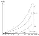
도 10은 최대 휘도 값에 따른 백색 광의 휘도 곡선들을 나타내는 도면이다.
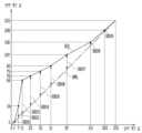
도 11은 백색 광 및 단색 광의 휘도 곡선들을 나타내는 도면이다.
도 12는 도 1의 표시 장치에 포함된 변환부의 일 예를 나타내는 블록도이다.
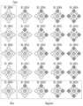
도 13은 제1 단위 영역을 기준으로 화소들의 발광 상태의 다양한 예들을 나타내는 도면이다.
도 14는 제2 단위 영역을 기준으로 화소들의 발광 상태의 다양한 예들을 나타내는 도면이다.
도 15는 제3 단위 영역을 기준으로 화소들의 발광 상태의 다양한 예들을 나타내는 도면이다.
도 16은 도 12의 변환부에 포함된 오프셋 설정부의 일 예를 나타내는 블록도이다.
도 17 및 도 18은 도 16의 오프셋 설정부에 포함된 단색 오프셋 제공부를 설명하기 위한 도면이다.
도 19는 도 1의 표시 장치에 포함된 화소의 휘도에 따른 노멀 블랙 전압들을 나타내는 룩업 테이블들이다.
도 20은 도 1의 표시 장치에 포함된 단위 영역 내 표시 색에 따른 화소들의 블랙 오프셋들을 나타내는 룩업 테이블이다.
도 21은 도 12의 변환부에 포함된 블랙 전압 레벨링부에서 생성된 룩업 테이블의 일 예를 나타내는 도면이다.
도 22는 도 12의 변환부에 포함된 중복 처리부의 동작을 설명하기 위한 도면이다.
도 23은 도 12의 변환부에 의해 최종 설정된 블랙 전압들을 나타내는 룩업 테이블이다.
도 24는 본 발명의 일 실시예에 따른 표시 장치의 구동 방법을 나타내는 순서도이다.FIG. 1 is a block diagram showing a display device according to one embodiment of the present invention.
FIG. 2 is a plan view showing an example of a pixel portion included in the display device of FIG. 1.
FIG. 3 is a circuit diagram showing an example of pixels included in the display device of FIG. 1.
Figure 4 is a waveform diagram showing the operation of the pixels of Figure 3.
FIG. 5 is a block diagram showing an example of the display device of FIG. 1.
Fig. 6 is a circuit diagram showing an example of pixels included in the display device of Fig. 5.
Figure 7 is a waveform diagram showing the operation of the pixels of Figure 6.
Fig. 8 is a drawing showing an example of a voltage generating unit included in the display device of Fig. 1.
Fig. 9 is a circuit diagram showing an example of a first voltage generator included in the voltage generator of Fig. 8.
Figure 10 is a diagram showing luminance curves of white light according to the maximum luminance value.
Figure 11 is a diagram showing the luminance curves of white light and monochromatic light.
Fig. 12 is a block diagram showing an example of a conversion unit included in the display device of Fig. 1.
Figure 13 is a drawing showing various examples of the light-emitting states of pixels based on the first unit area.
Figure 14 is a drawing showing various examples of the light-emitting states of pixels based on the second unit area.
Figure 15 is a drawing showing various examples of the light-emitting states of pixels based on the third unit area.
Fig. 16 is a block diagram showing an example of an offset setting unit included in the conversion unit of Fig. 12.
Figures 17 and 18 are drawings for explaining a single color offset providing unit included in the offset setting unit of Figure 16.
Figure 19 is a lookup table showing normal black voltages according to the luminance of pixels included in the display device of Figure 1.
Figure 20 is a lookup table showing black offsets of pixels according to display color within a unit area included in the display device of Figure 1.
FIG. 21 is a diagram showing an example of a lookup table generated in the black voltage leveling unit included in the conversion unit of FIG. 12.
Figure 22 is a drawing for explaining the operation of the duplicate processing unit included in the conversion unit of Figure 12.
Figure 23 is a lookup table showing the black voltages finally set by the conversion unit of Figure 12.
Figure 24 is a flowchart showing a method of driving a display device according to one embodiment of the present invention.
이하, 첨부한 도면을 참고로 하여 본 발명의 여러 실시 예들에 대하여 본 발명이 속하는 기술 분야에서 통상의 지식을 가진 자가 용이하게 실시할 수 있도록 상세히 설명한다. 본 발명은 여러 가지 상이한 형태로 구현될 수 있으며 여기에서 설명하는 실시 예들에 한정되지 않는다.Hereinafter, various embodiments of the present invention will be described in detail with reference to the attached drawings so that those skilled in the art can easily implement the present invention. The present invention may be implemented in various different forms and is not limited to the embodiments described herein.
본 발명을 명확하게 설명하기 위해서 설명과 관계없는 부분은 생략하였으며, 명세서 전체를 통하여 동일 또는 유사한 구성요소에 대해서는 동일한 참조 부호를 붙이도록 한다. 따라서 앞서 설명한 참조 부호는 다른 도면에서도 사용할 수 있다.In order to clearly explain the present invention, parts that are not related to the description are omitted, and the same reference numerals are used for identical or similar components throughout the specification. Accordingly, the reference numerals described above can also be used in other drawings.
또한, 도면에서 나타난 각 구성의 크기 및 두께는 설명의 편의를 위해 임의로 나타내었으므로, 본 발명이 반드시 도시된 바에 한정되지 않는다. 도면에서 여러 층 및 영역을 명확하게 표현하기 위하여 두께를 과장되게 나타낼 수 있다.In addition, the size and thickness of each component shown in the drawing are arbitrarily shown for convenience of explanation, so the present invention is not necessarily limited to what is shown. In order to clearly express various layers and areas in the drawing, the thickness may be exaggerated.
도 1은 본 발명의 일 실시예에 따른 표시 장치를 나타내는 블록도이다.FIG. 1 is a block diagram showing a display device according to one embodiment of the present invention.
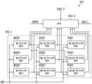
도 1을 참조하면, 표시 장치(10)는 프로세서(9)와 연결되며, 타이밍 제어부(11), 데이터 구동부(12)(또는, 소스 드라이버), 주사 구동부(13)(또는, 게이트 드라이버), 화소부(14)(또는, 표시 패널), 전압 생성부(15), 및 변환부(16)(또는, 보정부)를 포함할 수 있다.Referring to FIG. 1, the display device (10) is connected to a processor (9) and may include a timing control unit (11), a data driving unit (12) (or a source driver), a scan driving unit (13) (or a gate driver), a pixel unit (14) (or a display panel), a voltage generating unit (15), and a conversion unit (16) (or a correction unit).
프로세서(9)는 영상 프레임에 대한 입력 영상 데이터 및 제어 신호들을 제공할 수 있다. 입력 영상 데이터는 계조값들을 포함하며, 제어 신호는 수직 동기 신호, 수평 동기 신호, 클록 신호를 포함할 수 있다. 프로세서(9)는 어플리케이션 프로세서(application processor), CPU(central processing unit), GPU(graphics processing unit) 등을 포함할 수 있다. 프로세서(9)는 화소부(14)의 구조(예를 들어, 화소들(PX_T, PX_ADJ1, PX_ADJ2)의 배열로서, 펜타일(pentile) 구조, RGB 스트라이프(RGB stripe) 구조)에 매칭되는 계조값들을 표시 장치(10)에 제공할 수 있다. 예를 들어, 프로세서(9)는 화소부(14)에 포함된 화소들(PX_T, PX_ADJ1, PX_ADJ2)에 일대일 대응되는 계조값들을 표시 장치(10)에 제공할 수 있다. 이와 달리, 프로세서(9)는 화소부(14)의 구조와 무관하게 화소부(14)에 계조값들을 표시 장치(10)에 제공할 수도 있다. 예를 들어, 프로세서(9)는 풀 컬러(full color)를 표시하는 기본 단위인 하나의 도트(dot)에 대해 적색 계조값, 녹색 계조값, 및 청색 계조값을 제공할 수 있다. 이 경우, 프로세서(9)에서 제공되는 계조값들의 개수는 화소부(14)에 포함된 화소들(PX_T, PX_ADJ1, PX_ADJ2)의 개수와 다를 수 있다.The processor (9) can provide input image data and control signals for an image frame. The input image data includes grayscale values, and the control signal can include a vertical synchronization signal, a horizontal synchronization signal, and a clock signal. The processor (9) can include an application processor, a central processing unit (CPU), a graphics processing unit (GPU), etc. The processor (9) can provide grayscale values that match the structure of the pixel unit (14) (for example, an arrangement of pixels (PX_T, PX_ADJ1, PX_ADJ2), such as a pentile structure or an RGB stripe structure) to the display device (10). For example, the processor (9) can provide grayscale values that correspond one-to-one to pixels (PX_T, PX_ADJ1, PX_ADJ2) included in the pixel unit (14) to the display device (10). Alternatively, the processor (9) may provide the grayscale values to the display device (10) regardless of the structure of the pixel unit (14). For example, the processor (9) may provide a red grayscale value, a green grayscale value, and a blue grayscale value for one dot, which is a basic unit for displaying full color. In this case, the number of grayscale values provided by the processor (9) may be different from the number of pixels (PX_T, PX_ADJ1, PX_ADJ2) included in the pixel unit (14).
타이밍 제어부(11)는 프로세서(9)로부터 입력 영상 데이터 및 제어 신호들을 수신할 수 있다. 입력 영상 데이터가 화소부(14)의 구조에 매칭되는 계조값들을 포함하는 경우, 타이밍 제어부(11)는 계조값들을 변환부(16)에 전달할 수 있다. 입력 영상 데이터가 화소부(14)의 구조와 무관한 계조값들을 포함하는 경우, 타이밍 제어부(11)는 계조값들을 렌더링(rendering)하여 화소부(14)에 포함된 화소들과 일대일 대응되는 렌더링된 계조값들을 생성하고, 렌더링된 계조값들을 변환부(16)에 제공할 수 있다.The timing control unit (11) can receive input image data and control signals from the processor (9). If the input image data includes tone values that match the structure of the pixel unit (14), the timing control unit (11) can transfer the tone values to the conversion unit (16). If the input image data includes tone values that are unrelated to the structure of the pixel unit (14), the timing control unit (11) can render the tone values to generate rendered tone values that correspond one-to-one with pixels included in the pixel unit (14), and provide the rendered tone values to the conversion unit (16).
변환부(16)는 계조값들을 보정하여 변환 계조값들을 생성할 수 있다. 변환부(16)에 대해서는 화소부(14) 이후에 설명하기로 한다.The conversion unit (16) can generate converted grayscale values by correcting grayscale values. The conversion unit (16) will be described after the pixel unit (14).
타이밍 제어부(11)는 변환 계조값들 및 데이터 제어 신호(예를 들어, 수직 개시 신호에 대응하는 데이터 인에이블 신호)를 데이터 구동부(12)에 제공할 수 있다. 또한, 타이밍 제어부(11)는 주사 제어 신호(예를 들어, 클록 신호, 수직 개시 신호에 대응하는 주사 시작 신호)를 주사 구동부(13)에 제공할 수 있다.The timing control unit (11) can provide conversion grayscale values and a data control signal (e.g., a data enable signal corresponding to a vertical start signal) to the data driving unit (12). In addition, the timing control unit (11) can provide a scan control signal (e.g., a clock signal, a scan start signal corresponding to the vertical start signal) to the scan driving unit (13).
데이터 구동부(12)는 변환 계조값들 및 데이터 제어 신호에 기초하여 데이터 전압들을 생성하고, 데이터 전압들을 데이터 라인들(DL1, DL2, DL3, DLn, 단, n은 양의 정수)에 제공할 수 있다. 예를 들어, 데이터 구동부(12)는 클록 신호를 이용하여 변환 계조값들을 샘플링하고, 변환 계조값들에 대응하는 데이터 전압들을 화소행 단위로 데이터 라인들(DL1, DL2, DL3, DLn)에 제공할 수 있다. 예를 들어, 데이터 구동부(12)는 변환 계조값들 중 하나에 기초하여 전압 생성부(15)에서 제공되는 기준 전압들(RV1~RV255, RV0_1~RV0_256, GV1~GV255, GV0_1~GV0_256, BV1~BV255, BV0_1~BV0_256) 중 하나를 선택하고, 기준 전압들(RV1~RV255, RV0_1~RV0_256, GV1~GV255, GV0_1~GV0_256, BV1~BV255, BV0_1~BV0_256) 중 선택된 하나를 데이터 전압으로서 출력할 수 있다.The data driving unit (12) can generate data voltages based on the conversion grayscale values and the data control signal, and provide the data voltages to the data lines (DL1, DL2, DL3, DLn, where n is a positive integer). For example, the data driving unit (12) can sample the conversion grayscale values using a clock signal, and provide the data voltages corresponding to the conversion grayscale values to the data lines (DL1, DL2, DL3, DLn) in pixel row units. For example, the data driving unit (12) can select one of the reference voltages (RV1 to RV255, RV0_1 to RV0_256, GV1 to GV255, GV0_1 to GV0_256, BV1 to BV255, BV0_1 to BV0_256) provided from the voltage generating unit (15) based on one of the converted grayscale values, and output the selected one of the reference voltages (RV1 to RV255, RV0_1 to RV0_256, GV1 to GV255, GV0_1 to GV0_256, BV1 to BV255, BV0_1 to BV0_256) as a data voltage.
주사 구동부(13)는 주사 제어 신호에 기초하여 주사 신호들을 생성하고, 주사 신호들을 주사 라인들(SL1, SL2, SL3, SLm, 단, m은 양의 정수)에 제공할 수 있다. 예를 들어, 주사 구동부(13)는 주사 라인들(SL1, SL2, SL3, SLm)에 순차적으로 턴-온 레벨의 펄스를 갖는 주사 신호들을 제공할 수 있다. 여기서, 턴-온 레벨은 트랜지스터를 턴-온 시키는 전압 레벨일 수 있다. 예를 들어, 주사 구동부(13)는 복수의 스테이지 회로들을 포함하는 시프트 레지스터(shift register) 형태로 구성되고, 클록 신호에 응답하여 턴-온 레벨의 펄스를 가지는 주사 시작 신호를 현재 스테이지 회로로부터 다음 스테이지 회로에 순차적으로 전달하는 방식으로 주사 신호들을 생성할 수 있다.The scan driver (13) can generate scan signals based on a scan control signal, and provide the scan signals to scan lines (SL1, SL2, SL3, SLm, where m is a positive integer). For example, the scan driver (13) can sequentially provide scan signals having pulses of a turn-on level to the scan lines (SL1, SL2, SL3, SLm). Here, the turn-on level can be a voltage level that turns on a transistor. For example, the scan driver (13) is configured in the form of a shift register including a plurality of stage circuits, and can generate scan signals by sequentially transmitting a scan start signal having a pulse of a turn-on level from a current stage circuit to a next stage circuit in response to a clock signal.
화소부(14)는 화소들(PX_T, PX_ADJ1, PX_ADJ2)을 포함할 수 있다. 화소들(PX_T, PX_ADJ1, PX_ADJ2) 각각은 대응하는 데이터 라인 및 주사 라인에 연결될 수 있다.The pixel unit (14) may include pixels (PX_T, PX_ADJ1, PX_ADJ2). Each of the pixels (PX_T, PX_ADJ1, PX_ADJ2) may be connected to a corresponding data line and scan line.
화소부(14)는 제1 색으로 발광하는 제1 색 화소들, 제2 색으로 발광하는 제2 색 화소들, 및 제3 색으로 발광하는 제3 색 화소들을 포함할 수 있다. 제1 색, 제2 색, 및 제3 색은 서로 다른 색들일 수 있다. 예를 들어, 제1 색은 적색, 녹색, 및 청색 중 한가지 색이고, 제2 색은 적색, 녹색, 및 청색 중 다른 색이며, 제3 색은 적색, 녹색, 및 청색 중 또 다른 색일 수 있다. 또한, 제1 내지 제3 색들로 적색, 녹색, 및 청색 대신 마젠타(magenta), 시안(cyan), 및 옐로우(yellow)가 사용될 수도 있다. 다만, 설명의 편의상, 제1 내지 제3 색들로 적색, 녹색, 및 청색이 사용되며, 마젠타는 적색 및 청색의 조합, 시안은 녹색 및 청색의 조합, 옐로우는 적색 및 녹색의 조합으로 표현되는 것으로 설명한다.The pixel unit (14) may include first color pixels that emit light with a first color, second color pixels that emit light with a second color, and third color pixels that emit light with a third color. The first color, the second color, and the third color may be different colors. For example, the first color may be one of red, green, and blue, the second color may be another color of red, green, and blue, and the third color may be another color of red, green, and blue. In addition, magenta, cyan, and yellow may be used instead of red, green, and blue as the first to third colors. However, for convenience of explanation, it is explained that red, green, and blue are used as the first to third colors, and magenta is expressed as a combination of red and blue, cyan is expressed as a combination of green and blue, and yellow is expressed as a combination of red and green.
실시예들에서, 화소부(14)는 대상 화소(PX_T) 및 주변 화소들(PX_ADJ1, PX_ADJ2)을 포함할 수 있다. 여기서, 대상 화소(PX_T)는 변환부(16)에서 변환 계조값을 생성함에 있어서 기준이 되는 화소이며, 주변 화소들(PX_ADJ1, PX_ADJ2)은 대상 화소(PX_T)를 기준으로 설정된 단위 영역(OA) 내에 위치하는 화소들이며, 주변 화소들(PX_ADJ1, PX_ADJ2)은 대상 화소에 인접할 수 있다. 대상 화소(PX_T) 및 주변 화소들(PX_ADJ1, PX_ADJ2) 사이에는 다른 화소가 배치되지 않으며, 대상 화소(PX_T) 및 주변 화소들(PX_ADJ1, PX_ADJ2)은 상호 측면 누출의 영향을 받을 수 있다. 예를 들어, 대상 화소(PX_T)의 발광 다이오드를 통해 주변 화소들(PX_ADJ1, PX_ADJ2)로 구동 전류가 누출되거나 주변 화소들(PX_ADJ1, PX_ADJ2)로부터 구동 전류가 유입될 수 있다.In the embodiments, the pixel unit (14) may include a target pixel (PX_T) and surrounding pixels (PX_ADJ1, PX_ADJ2). Here, the target pixel (PX_T) is a reference pixel for generating a conversion grayscale value in the conversion unit (16), and the surrounding pixels (PX_ADJ1, PX_ADJ2) are pixels located within a unit area (OA) set based on the target pixel (PX_T), and the surrounding pixels (PX_ADJ1, PX_ADJ2) may be adjacent to the target pixel. No other pixels are arranged between the target pixel (PX_T) and the surrounding pixels (PX_ADJ1, PX_ADJ2), and the target pixel (PX_T) and the surrounding pixels (PX_ADJ1, PX_ADJ2) may be affected by mutual lateral leakage. For example, driving current may leak to surrounding pixels (PX_ADJ1, PX_ADJ2) through the light-emitting diode of the target pixel (PX_T), or driving current may flow in from the surrounding pixels (PX_ADJ1, PX_ADJ2).
이하에서, 화소들(PX_T, PX_ADJ1, PX_ADJ2) 각각의 위치는 발광 다이오드(특히, 발광 층)의 위치를 기준으로 설명된다. 각각의 발광 다이오드에 연결된 화소 회로의 위치는 발광 다이오드의 위치와 대응하지 않을 수 있으며, 공간 효율성을 위해 화소부(14) 내에서 적절히 배치될 수 있다.Hereinafter, the positions of each of the pixels (PX_T, PX_ADJ1, PX_ADJ2) are described based on the positions of the light-emitting diodes (particularly, the light-emitting layer). The positions of the pixel circuits connected to each light-emitting diode may not correspond to the positions of the light-emitting diodes, and may be appropriately arranged within the pixel portion (14) for space efficiency.
단위 영역(OA), 대상 화소(PX_T), 및 주변 화소들(PX_ADJ1, PX_ADJ2)에 대해서는 도 2를 참조하여 후술하기로 한다.The unit area (OA), target pixel (PX_T), and surrounding pixels (PX_ADJ1, PX_ADJ2) will be described later with reference to Fig. 2.
전압 생성부(15)는 입력 최대 휘도 값(DBV)을 수신하고, 입력 최대 휘도 값(DBV)에 대응하는 제1 색의 화소들에 대한 제1 기준 전압들(RV1~RV255, RV0_1~RV0_256)(또는, 제1 계조 전압들, 제1 감마 전압들), 제2 색의 화소들에 대한 제2 기준 전압들(GV1~GV255, GV0_1~GV0_256), 및 제3 색의 화소들에 대한 제3 기준 전압들(BV1~BV255, BV0_1~BV0_256)을 제공할 수 있다. 여기서, 제1 기준 전압들(RV1~RV255, RV0_1~RV0_256)은 제1 기준 감마 전압들(RV1~RV255) 및 제1 기준 블랙 전압들(RV0_1~RV0_256)을 포함하고, 제1 기준 감마 전압들(RV1~RV255)은 0 내지 255 범위의 계조들 중 1 내지 255의 범위의 계조들에 대응하며, 제1 기준 블랙 전압들(RV0_1~RV0_256) 중 선택된 하나는 0의 계조에 대응할 수 있다. 유사하게, 제2 기준 전압들(GV1~GV255, GV0_1~GV0_256)은 제2 기준 감마 전압들(GV1~GV255) 및 제2 기준 블랙 전압들(GV0_1~GV0_256)을 포함하고, 제3 기준 전압들(BV1~BV255, BV0_1~BV0_256)은 제3 기준 감마 전압들(BV1~BV255) 및 제3 기준 블랙 전압들(BV0_1~BV0_256)을 포함할 수 있다.The voltage generator (15) can receive an input maximum brightness value (DBV) and provide first reference voltages (RV1 to RV255, RV0_1 to RV0_256) (or, first grayscale voltages, first gamma voltages) for pixels of a first color corresponding to the input maximum brightness value (DBV), second reference voltages (GV1 to GV255, GV0_1 to GV0_256) for pixels of a second color, and third reference voltages (BV1 to BV255, BV0_1 to BV0_256) for pixels of a third color. Here, the first reference voltages (RV1 to RV255, RV0_1 to RV0_256) include first reference gamma voltages (RV1 to RV255) and first reference black voltages (RV0_1 to RV0_256), and the first reference gamma voltages (RV1 to RV255) correspond to grayscales in a range of 1 to 255 among grayscales in a range of 0 to 255, and a selected one of the first reference black voltages (RV0_1 to RV0_256) can correspond to a grayscale of 0. Similarly, the second reference voltages (GV1 to GV255, GV0_1 to GV0_256) may include second reference gamma voltages (GV1 to GV255) and second reference black voltages (GV0_1 to GV0_256), and the third reference voltages (BV1 to BV255, BV0_1 to BV0_256) may include third reference gamma voltages (BV1 to BV255) and third reference black voltages (BV0_1 to BV0_256).
설명의 편의상, 계조값들은 0의 계조(즉, 최소 계조)으로부터 255의 계조(즉, 최대 계조값)까지 총 256개의 계조들을 포함하는 것으로 설명하나, 이에 한정되는 것은 아니다. 예를 들어, 계조값들 각각을 8 비트 이상으로 표현하는 경우 더 많은 계조들이 존재할 수도 있다. 최소 계조는 가장 어두운 계조(예를 들어, 블랙 계조)이며, 최대 계조는 가장 밝은 계조일 수 있다.For convenience of explanation, the grayscale values are described as including a total of 256 grayscales from a grayscale of 0 (i.e., the minimum grayscale) to a grayscale of 255 (i.e., the maximum grayscale), but are not limited thereto. For example, if each grayscale value is expressed with 8 bits or more, there may be more grayscales. The minimum grayscale may be the darkest grayscale (e.g., the black grayscale), and the maximum grayscale may be the brightest grayscale.
최대 휘도 값은 최대 계조에 대응하여 화소부(14)(또는, 단위 영역(OA), 화소들(PX_T, PX_ADJ1, PX_ADJ2))에서 방출되는 광의 휘도 값일 수 있다. 예를 들어, 하나의 도트(dot)를 이루는 제1 색의 화소가 255 계조에 대응하여 발광하고, 제2 색의 화소가 255 계조에 대응하여 발광하고, 및 제3 색의 화소가 255 계조에 대응하여 발광하는 경우, 제1 내지 제3 색들의 조합에 의한 광, 즉, 백색 광의 휘도 값이 최대 휘도 값일 수 있다. 휘도 값의 단위는 니트(nit)일 수 있다.The maximum luminance value may be the luminance value of light emitted from the pixel portion (14) (or, unit area (OA), pixels (PX_T, PX_ADJ1, PX_ADJ2)) corresponding to the maximum grayscale. For example, when a pixel of a first color forming one dot emits light corresponding to 255 grayscale, a pixel of a second color emits light corresponding to 255 grayscale, and a pixel of a third color emits light corresponding to 255 grayscale, the luminance value of light by a combination of the first to third colors, that is, white light, may be the maximum luminance value. The unit of the luminance value may be nit.
따라서, 화소부(14)는 부분적으로(또는, 공간적으로) 어둡거나 밝은 영상 프레임을 표시할 수 있지만, 영상 프레임의 최대 밝기는 최대 휘도 값으로 제한되게 된다. 최대 휘도 값은 표시 장치(10)에 대한 사용자의 조작에 의해 수동적으로 설정되거나, 조도 센서 등과 연계된 알고리즘에 의해 자동적으로 설정될 수 있다. 이러한 방식으로 설정된 최대 휘도 값을 입력 최대 휘도 값이라고 표현한다.Accordingly, the pixel unit (14) can display a partially (or spatially) dark or bright image frame, but the maximum brightness of the image frame is limited to a maximum brightness value. The maximum brightness value can be manually set by a user's operation on the display device (10), or automatically set by an algorithm linked to a light sensor or the like. The maximum brightness value set in this manner is expressed as an input maximum brightness value.
예를 들어, 휘도의 최대 값은 1200 니트이고, 최소 값은 4 니트일 수 있다. 계조값이 동일하더라도, 입력 최대 휘도 값(DBV)이 달라지면, 전압 생성부(15)에서 생성되는 기준 전압들(RV1~RV255, RV0_1~RV0_256, GV1~GV255, GV0_1~GV0_256, BV1~BV255, BV0_1~BV0_256)이 변하고, 이에 따라 화소부(14)(또는, 화소들(PX_T, PX_ADJ1, PX_ADJ2))의 휘도도 변하게 된다.For example, the maximum value of the luminance may be 1200 nits, and the minimum value may be 4 nits. Even if the grayscale value is the same, if the input maximum luminance value (DBV) changes, the reference voltages (RV1 to RV255, RV0_1 to RV0_256, GV1 to GV255, GV0_1 to GV0_256, BV1 to BV255, BV0_1 to BV0_256) generated from the voltage generation unit (15) change, and accordingly, the luminance of the pixel unit (14) (or, pixels (PX_T, PX_ADJ1, PX_ADJ2)) also changes.
변환부(16)는 단위 영역(OA) 내 주변 화소들(PX_ADJ1, PX_ADJ2)의 계조값들에 기초하여 주변 화소들(PX_ADJ1, PX_ADJ2)의 발광 상태를 결정하고, 발광 상태에 기초하여 대상 화소(PX_T)에 대한 계조값을 보정하여 보정된 계조값을 생성할 수 있다. 이하에서는, 설명의 편의상, 대상 화소(PX_T)에 대한 계조값을 입력 계조값으로 지칭하고, 주변 화소들(PX_ADJ1, PX_ADJ2)에 대한 계조값들을 관찰 계조값들로 지칭하기로 한다.The conversion unit (16) can determine the light emission status of the surrounding pixels (PX_ADJ1, PX_ADJ2) based on the light emission status of the surrounding pixels (PX_ADJ1, PX_ADJ2) within the unit area (OA), and can correct the light emission status of the target pixel (PX_T) to generate a corrected light emission value. Hereinafter, for convenience of explanation, the light emission status of the target pixel (PX_T) will be referred to as an input light emission value, and the light emission status of the surrounding pixels (PX_ADJ1, PX_ADJ2) will be referred to as observed light emission values.
또한, 변환부(16)는 주변 화소들(PX_ADJ1, PX_ADJ2)의 발광 상태들에 기초하여 주변 화소들(PX_ADJ1, PX_ADJ2) 중 비발광하는 적어도 하나의 주변 화소에 대한 블랙 계조값(또는, 블랙 전압)을 결정 할 수 있다. 여기서, 블랙 계조값은, 주변 화소들(PX_ADJ1, PX_ADJ2)이 비발광하는 경우, 비발광하는 주변 화소들(PX_ADJ1, PX_ADJ2)에 제공되는 데이터 전압(예를 들어, 최소 계조에 대응하는 데이터 전압)의 전압 레벨을 나타내는 계조값이다. 블랙 계조값에 기초하여 전압 생성부(15)에서 생성된 블랙 전압들(RV0_1~RV0_256, GV0_1~GV0_256, BV0_1~BV0_256) 중 하나의 블랙 전압이 선택되고, 선택된 하나의 블랙 전압은 비발광하는 해당 화소에 데이터 전압으로서 제공될 수 있다. 보정된 계조값 및 블랙 계조값은 변환 계조값에 포함될 수 있다. 예를 들어, 8비트의 보정된 계조값 및 8비트의 블랙 계조값은 9비트의 변환 계조값으로 표현될 수 있다.In addition, the conversion unit (16) can determine a black grayscale value (or black voltage) for at least one non-emitting peripheral pixel among the peripheral pixels (PX_ADJ1, PX_ADJ2) based on the emission states of the peripheral pixels (PX_ADJ1, PX_ADJ2). Here, the black grayscale value is a grayscale value representing a voltage level of a data voltage (for example, a data voltage corresponding to a minimum grayscale) provided to the non-emitting peripheral pixels (PX_ADJ1, PX_ADJ2) when the peripheral pixels (PX_ADJ1, PX_ADJ2) do not emit light. Based on the black grayscale value, one of the black voltages (RV0_1 to RV0_256, GV0_1 to GV0_256, BV0_1 to BV0_256) generated by the voltage generation unit (15) is selected, and the selected one black voltage can be provided as a data voltage to the corresponding non-emitting pixel. The corrected tone value and black tone value can be included in the converted tone value. For example, the 8-bit corrected tone value and the 8-bit black tone value can be expressed as a 9-bit converted tone value.
실시예들에서, 변환부(16)는 계조 변환부(161)(또는, 계조 보정부) 및 블랙 전압 변환부(162)(또는, 블랙 전압 보정부)를 포함할 수 있다.In embodiments, the conversion unit (16) may include a grayscale conversion unit (161) (or, grayscale correction unit) and a black voltage conversion unit (162) (or, black voltage correction unit).
계조 변환부(161)는 단위 영역(OA) 내 주변 화소들(PX_ADJ1, PX_ADJ2)의 발광 상태들(또는, 색상별 발광 화소 개수)을 각각 결정하고, 발광 상태들에 기초하여 대상 화소(PX_T)에 대한 입력 계조값을 보정할 수 있다. 여기서, 발광 상태들은 주변 화소들(PX_ADJ1, PX_ADJ2)의 발광 또는 비발광 여부를 각각 나타내며, 발광 상태들에 기초하여 단위 영역(OA)이 단색 광(single color light), 이중 혼색 광(double mixed color light), 삼중 혼색 광(triple mixed color light), 또는 백색 광(white color light)을 방출하는 지가 결정될 수 있다.The grayscale conversion unit (161) can determine the emission states (or the number of emission pixels by color) of the surrounding pixels (PX_ADJ1, PX_ADJ2) within the unit area (OA), and correct the input grayscale value for the target pixel (PX_T) based on the emission states. Here, the emission states indicate whether the surrounding pixels (PX_ADJ1, PX_ADJ2) emit or do not emit light, respectively, and based on the emission states, it can be determined whether the unit area (OA) emits single color light, double mixed color light, triple mixed color light, or white color light.
블랙 전압 변환부(162)는 단위 영역(OA) 내 주변 화소들(PX_ADJ1, PX_ADJ2)의 발광 상태들에 기초하여 주변 화소들(PX_ADJ1, PX_ADJ2)의 블랙 계조값(또는, 블랙 전압의 전압 레벨)을 설정할 수 있다.The black voltage converter (162) can set the black grayscale value (or voltage level of the black voltage) of the surrounding pixels (PX_ADJ1, PX_ADJ2) based on the light emission states of the surrounding pixels (PX_ADJ1, PX_ADJ2) within the unit area (OA).
예를 들어, 단위 영역(OA)이 제1 색 화소들(예를 들어, 적색 화소들) 및 제2 화소들(예를 들어, 녹색 화소들)을 포함하고, 제1 색 화소들 중 적어도 하나가 발광하고 제2 색 화소들이 모두 비발광하는 경우, 계조 변환부(161)는 제2 화소들에 대한 블랙 전압이 상대적으로 높아지도록(즉, 제2 색 화소들 중 적어도 하나가 발광하는 경우에서의 블랙 전압보다 높아지도록), 블랙 계조값을 설정할 수 있다. 다른 예로, 단위 영역(OA) 내에서 제2 색 화소들 중 적어도 하나가 발광하고 제1 색 화소들이 모두 비발광하는 경우, 계조 변환부(161)는 제1 화소들에 대한 블랙 전압이 상대적으로 높아지도록(즉, 제1 색 화소들 중 적어도 하나가 발광하는 경우에서의 블랙 전압보다 높아지도록), 블랙 계조값을 설정할 수 있다.For example, if the unit area (OA) includes first color pixels (e.g., red pixels) and second color pixels (e.g., green pixels), and at least one of the first color pixels emits light and all of the second color pixels do not emit light, the grayscale conversion unit (161) can set the black grayscale value so that the black voltage for the second pixels becomes relatively high (i.e., higher than the black voltage in the case where at least one of the second color pixels emits light). As another example, if at least one of the second color pixels emits light and all of the first color pixels do not emit light in the unit area (OA), the grayscale conversion unit (161) can set the black grayscale value so that the black voltage for the first pixels becomes relatively high (i.e., higher than the black voltage in the case where at least one of the first color pixels emits light).
한편, 단위 영역(OA)이 제3 색 화소들(예를 들어, 청색 화소들)을 포함하는 경우, 블랙 전압 변환부(162)는, 제1 색 및 제2 색 화소들의 발광 상태들과 무관하게, 동일한 휘도 조건 하에서 제3 색 화소들의 블랙 전압이 일정하게 유지되도록, 블랙 계조값을 설정할 수도 있다.Meanwhile, when the unit area (OA) includes third color pixels (e.g., blue pixels), the black voltage converter (162) may set the black gradation value so that the black voltage of the third color pixels remains constant under the same luminance conditions, regardless of the emission states of the first color and second color pixels.
변환부(16)의 보다 구체적인 구성 및 동작에 대해서는 도 12를 참조하여 후술하기로 한다.A more specific configuration and operation of the converter (16) will be described later with reference to Fig. 12.
한편, 도 1에서 변환부(16)는 타이밍 제어부(11)와 별도의 구성으로 도시되었다. 그러나, 실시예에 따라, 변환부(16)의 적어도 일부는 타이밍 제어부(11)와 일체로 구성될 수 있다. 예를 들어, 변환부(16)의 적어도 일부는 타이밍 제어부(11)와 함께 집적 회로(integrated circuit) 형태로 구성될 수도 있다. 실시예에 따라, 변환부(16)의 적어도 일부는 타이밍 제어부(11)에서 소프트웨어적으로 구현될 수도 있다.Meanwhile, in FIG. 1, the conversion unit (16) is illustrated as a separate configuration from the timing control unit (11). However, depending on the embodiment, at least a part of the conversion unit (16) may be configured integrally with the timing control unit (11). For example, at least a part of the conversion unit (16) may be configured in the form of an integrated circuit together with the timing control unit (11). Depending on the embodiment, at least a part of the conversion unit (16) may be implemented in software in the timing control unit (11).
다른 실시예에서, 변환부(16)의 적어도 일부는 데이터 구동부(12)와 함께 집적 회로 형태로 구성될 수도 있다. 실시예에 따라, 변환부(16)의 적어도 일부는 데이터 구동부(12)에서 소프트웨어적으로 구현될 수도 있다.In another embodiment, at least a portion of the conversion unit (16) may be configured in the form of an integrated circuit together with the data driving unit (12). Depending on the embodiment, at least a portion of the conversion unit (16) may be implemented in software in the data driving unit (12).
또 다른 실시예에서, 변환부(16)는 적어도 일부는 프로세서(9)와 함께 집적 회로 형태로 구성될 수도 있다.In another embodiment, the converter (16) may be configured in the form of an integrated circuit, at least in part, together with the processor (9).
도 1을 참조하여 설명한 바와 같이, 표시 장치(10)는 대상 화소(PX_T)를 기준으로 설정된 단위 영역(OA) 내 주변 화소들(PX_ADJ1, PX_ADJ2)의 발광 상태에 기초하여, 대상 화소(PX_T)의 입력 계조값을 보정하고 주변 화소들(PX_ADJ1, PX_ADJ2)의 블랙 전압을 가변시킬 수 있다. 따라서, 측면 누출이 방지되고, 화소부(14)가 단색 광 및 혼색 광들의 영상을 표시하는 경우에도 목표하는 휘도가 발휘될 수 있다.As described with reference to FIG. 1, the display device (10) can correct the input grayscale value of the target pixel (PX_T) and vary the black voltage of the surrounding pixels (PX_ADJ1, PX_ADJ2) within the unit area (OA) set based on the target pixel (PX_T). Accordingly, side leakage is prevented, and the target brightness can be achieved even when the pixel portion (14) displays an image of monochromatic light and mixed-color light.
도 2는 도 1의 표시 장치에 포함된 화소부의 일 예를 나타내는 평면도이다. 도 2에는 화소부(14)의 일부가 예시적으로 도시되어 있다.Fig. 2 is a plan view showing an example of a pixel portion included in the display device of Fig. 1. Fig. 2 illustrates a part of a pixel portion (14) as an example.
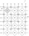
도 2를 참조하면, 화소들(RP22, RP26, RP44, RP62, RP66, RP84, GP11, GP13, GP15, GP17, GP31, GP33, GP35, GP37, GP51, GP53, GP55, GP57, GP71, GP73, GP75, GP77, BP24, BP42, BP46, BP64, BP82, BP86)은 발광 다이오드의 위치를 기준으로 도시되었으며, 주사 라인들(SL1~SL8) 및 데이터 라인들(DL1~DL7)은 화소부(14)의 전기적인 연결 관계를 설명하기 위하여 간략히 도시되었다.Referring to FIG. 2, pixels (RP22, RP26, RP44, RP62, RP66, RP84, GP11, GP13, GP15, GP17, GP31, GP33, GP35, GP37, GP51, GP53, GP55, GP57, GP71, GP73, GP75, GP77, BP24, BP42, BP46, BP64, BP82, BP86) are illustrated based on the positions of light-emitting diodes, and scan lines (SL1 to SL8) and data lines (DL1 to DL7) are briefly illustrated to explain the electrical connection relationship of the pixel portion (14).
화소들(RP22, RP26, RP44, RP62, RP66, RP84, GP11, GP13, GP15, GP17, GP31, GP33, GP35, GP37, GP51, GP53, GP55, GP57, GP71, GP73, GP75, GP77, BP24, BP42, BP46, BP64, BP82, BP86)은 제1 색 화소들(RP22, RP26, RP44, RP62, RP66, RP84), 제2 색 화소들(GP11, GP13, GP15, GP17, GP31, GP33, GP35, GP37, GP51, GP53, GP55, GP57, GP71, GP73, GP75, GP77), 및 제3 색 화소들(BP24, BP42, BP46, BP64, BP82, BP86)을 포함할 수 있다.Pixels (RP22, RP26, RP44, RP62, RP66, RP84, GP11, GP13, GP15, GP17, GP31, GP33, GP35, GP37, GP51, GP53, GP55, GP57, GP71, GP73, GP75, GP77, BP24, BP42, BP46, BP64, BP82, BP86) are first color pixels (RP22, RP26, RP44, RP62, RP66, RP84), second color pixels (GP11, GP13, GP15, GP17, GP31, GP33, GP35, GP37, GP51, GP53, GP55, GP57, GP71, GP73, GP75, GP77), and third color pixels (BP24, BP42, BP46, BP64, BP82, BP86).
제1 색 화소들(RP22, RP26, RP44, RP62, RP66, RP84)은 제1 색으로 발광하며, 예를 들어, 제1 색은 적색일 수 있다. 제2 색 화소들(GP11, GP13, GP15, GP17, GP31, GP33, GP35, GP37, GP51, GP53, GP55, GP57, GP71, GP73, GP75, GP77)은 제2 색으로 발광하며, 예를 들어, 제2 색은 녹색일 수 있다. 제3 색 화소들(BP24, BP42, BP46, BP64, BP82, BP86)은 제3 색으로 발광하며, 예를 들어, 제3 색은 청색일 수 있다.The first color pixels (RP22, RP26, RP44, RP62, RP66, RP84) emit light with a first color, for example, the first color can be red. The second color pixels (GP11, GP13, GP15, GP17, GP31, GP33, GP35, GP37, GP51, GP53, GP55, GP57, GP71, GP73, GP75, GP77) emit light with a second color, for example, the second color can be green. The third color pixels (BP24, BP42, BP46, BP64, BP82, BP86) emit light with a third color, for example, the third color can be blue.
실시예들에서, 제1 색 화소들(RP22, RP26, RP44, RP62, RP66, RP84), 제2 색 화소들(GP11, GP13, GP15, GP17, GP31, GP33, GP35, GP37, GP51, GP53, GP55, GP57, GP71, GP73, GP75, GP77), 및 제3 색 화소들(BP24, BP42, BP46, BP64, BP82, BP86)은 RGBG 다이아몬드 펜타일(diamond pentile) 구조로 배열될 수 있다.In the embodiments, the first color pixels (RP22, RP26, RP44, RP62, RP66, RP84), the second color pixels (GP11, GP13, GP15, GP17, GP31, GP33, GP35, GP37, GP51, GP53, GP55, GP57, GP71, GP73, GP75, GP77), and the third color pixels (BP24, BP42, BP46, BP64, BP82, BP86) may be arranged in an RGBG diamond pentile structure.
제1 색 화소들(RP22, RP26, RP44, RP62, RP66, RP84), 제2 색 화소들(GP11, GP13, GP15, GP17, GP31, GP33, GP35, GP37, GP51, GP53, GP55, GP57, GP71, GP73, GP75, GP77), 및 제3 색 화소들(BP24, BP42, BP46, BP64, BP82, BP86) 각각은 주사 라인들(SL1~SL8) 중 대응되는 주사 라인 및 데이터 라인들(DL1~DL7) 중 대응되는 데이터 라인에 연결될 수 있다.Each of the first color pixels (RP22, RP26, RP44, RP62, RP66, RP84), the second color pixels (GP11, GP13, GP15, GP17, GP31, GP33, GP35, GP37, GP51, GP53, GP55, GP57, GP71, GP73, GP75, GP77), and the third color pixels (BP24, BP42, BP46, BP64, BP82, BP86) can be connected to a corresponding scan line among the scan lines (SL1 to SL8) and a corresponding data line among the data lines (DL1 to DL7).
한편, 도 2에서 홀수 번째 주사 라인들(SL1, SL3, SL5, SL7)은 제2 색 화소들(GP11, GP13, GP15, GP17, GP31, GP33, GP35, GP37, GP51, GP53, GP55, GP57, GP71, GP73, GP75, GP77)에 연결되고, 짝수 번째 주사 라인들(SL2, SL4, SL6, SL8)은 제1 색 화소들(RP22, RP26, RP44, RP62, RP66, RP84) 및 제3 색 화소들(BP24, BP42, BP46, BP64, BP82, BP86)에 연결되는 것으로 도시되어 있으나, 이에 한정되는 것은 아니다. 예를 들어, 제2 주사 라인(SL2)은 제1 주사 라인(SL1)과 연결되거나 제1 주사 라인(SL1) 및 제2 주사 라인(SL2)은 하나의 주사 라인으로 구성되고, 제1 주사 라인(SL1) 및 제2 주사 라인(SL2)에는 동일한 주사 신호가 제공될 수 있다.Meanwhile, in FIG. 2, odd-numbered scan lines (SL1, SL3, SL5, SL7) are illustrated as being connected to second color pixels (GP11, GP13, GP15, GP17, GP31, GP33, GP35, GP37, GP51, GP53, GP55, GP57, GP71, GP73, GP75, GP77), and even-numbered scan lines (SL2, SL4, SL6, SL8) are illustrated as being connected to first color pixels (RP22, RP26, RP44, RP62, RP66, RP84) and third color pixels (BP24, BP42, BP46, BP64, BP82, BP86), but are not limited thereto. For example, the second scanning line (SL2) may be connected to the first scanning line (SL1), or the first scanning line (SL1) and the second scanning line (SL2) may be configured as one scanning line, and the same scanning signal may be provided to the first scanning line (SL1) and the second scanning line (SL2).
제44 화소(RP44)(즉, 4번째 행 및 4번째 열에 배치되는 제1 색 화소)가 도 1을 참조하여 설명한 대상 화소(PX_T)인 경우, 제1 단위 영역(ORA)은 제44 화소(RP44)를 기준으로 제1 반경 이내의 영역으로 설정되며, 제44 화소(RP44)의 주변 화소들은, 제1 단위 영역(ORA) 내 제24 화소(BP24), 제33 화소(GP33), 제35 화소(GP35), 제42 화소(BP42), 제46화소(BP46), 제53 화소(GP53), 제55 화소(GP55), 및 제64 화소(BP64)를 포함할 수 있다. 예를 들어, 제1 반경은 제44 화소(RP44)로부터, 제44 화소(RP44)와 동일한 색으로 발광하며 제44 화소(RP44)에 인접한 제22 화소(RP22)(또는, 제26 화소(RP26), 제62 화소(RP62), 제66 화소(RP66))까지의 거리(예를 들어, 화소 중심들 간의 거리)에 대응할 수 있다.When the 44th pixel (RP44) (i.e., the first color pixel arranged in the 4th row and the 4th column) is the target pixel (PX_T) described with reference to FIG. 1, the first unit area (ORA) is set as an area within a first radius based on the 44th pixel (RP44), and the pixels surrounding the 44th pixel (RP44) may include the 24th pixel (BP24), the 33rd pixel (GP33), the 35th pixel (GP35), the 42nd pixel (BP42), the 46th pixel (BP46), the 53rd pixel (GP53), the 55th pixel (GP55), and the 64th pixel (BP64) within the first unit area (ORA). For example, the first radius may correspond to a distance (e.g., a distance between pixel centers) from a 44th pixel (RP44) to a 22nd pixel (RP22) (or a 26th pixel (RP26), a 62nd pixel (RP62), or a 66th pixel (RP66)) adjacent to the 44th pixel (RP44) and emitting the same color as the 44th pixel (RP44).
제55 화소(GP55)(즉, 5번째 행 및 5번째 열에 배치되는 제2 색 화소)가 대상 화소(PX_T)인 경우, 제2 단위 영역(OGA)은 제55 화소(GP55)를 기준으로 제2 반경 이내의 영역으로 설정될 수 있다. 예를 들어, 제2 반경은 제55 화소(GP55)로부터, 제55 화소(GP55)와 동일한 색으로 발광하며 제55 화소(GP55)에 인접한 제35 화소(GP35)(또는, 제53 화소(GP53), 제57 화소(GP57), 제75 화소(GP75))까지의 거리에 대응할 수 있다. 이 경우, 제55 화소(GP55)의 주변 화소들은, 제2 단위 영역(OGA) 내 제44 화소(RP44), 제46 화소(BP46), 제64 화소(BP64), 및 제66 화소(RP66)를 포함할 수 있다.When the 55th pixel (GP55) (i.e., the second color pixel arranged in the 5th row and the 5th column) is the target pixel (PX_T), the second unit area (OGA) may be set as an area within a second radius based on the 55th pixel (GP55). For example, the second radius may correspond to the distance from the 55th pixel (GP55) to the 35th pixel (GP35) (or, the 53rd pixel (GP53), the 57th pixel (GP57), and the 75th pixel (GP75)) that emits the same color as the 55th pixel (GP55) and is adjacent to the 55th pixel (GP55). In this case, the pixels surrounding the 55th pixel (GP55) may include the 44th pixel (RP44), the 46th pixel (BP46), the 64th pixel (BP64), and the 66th pixel (RP66) within the second unit area (OGA).
유사하게, 제64 화소(BP64)(즉, 6번째 행 및 4번째 열에 배치되는 제3 색 화소)가 대상 화소(PX_T)인 경우, 제3 단위 영역(OBA)은 제64 화소(BP64)를 기준으로 제3 반경 이내의 영역으로 설정될 수 있다. 예를 들어, 제3 반경은 제64 화소(BP44)로부터 제42 화소(BP42)까지의 거리에 대응할 수 있다. 이 경우, 제64 화소(BP44)의 주변 화소들은, 제3 단위 영역(OBA) 내 제44 화소(RP44), 제53 화소(GP53), 제55 화소(GP55), 제62 화소(RP62), 제66화소(RP66), 제73 화소(GP73), 제75 화소(GP75), 및 제84 화소(RP84)를 포함할 수 있다.Similarly, when the 64th pixel (BP64) (i.e., the third color pixel arranged in the 6th row and the 4th column) is the target pixel (PX_T), the third unit area (OBA) may be set as an area within a third radius based on the 64th pixel (BP64). For example, the third radius may correspond to the distance from the 64th pixel (BP44) to the 42nd pixel (BP42). In this case, the surrounding pixels of the 64th pixel (BP44) may include the 44th pixel (RP44), the 53rd pixel (GP53), the 55th pixel (GP55), the 62nd pixel (RP62), the 66th pixel (RP66), the 73rd pixel (GP73), the 75th pixel (GP75), and the 84th pixel (RP84) within the third unit area (OBA).
한편, 도 2에서 제1 색 화소들(RP22, RP26, RP44, RP62, RP66, RP84), 제2 색 화소들(GP11, GP13, GP15, GP17, GP31, GP33, GP35, GP37, GP51, GP53, GP55, GP57, GP71, GP73, GP75, GP77), 및 제3 색 화소들(BP24, BP42, BP46, BP64, BP82, BP86)은 RGBG 다이아몬드 펜타일 구조로 배열되는 것으로 도시되었으나, 이에 한정되는 것은 아니다. 예를 들어, 화소들은 다른 구조, 예를 들어, RGB-스트라이프(RGB-Stripe), S-스트라이프(S-stripe), 리얼 RGB(Real RGB), 일반 펜타일(normal pentile) 등의 형태로 배치될 수 있다. 이 경우, 단위 영역들(ORA, OGA, OBA) 각각은 대상 화소(PX_T)와 인접하여 배치되되 대상 화소(PT_T)와 다른 색상으로 발광하는 주변 화소들을 포함하도록 적절히 설정될 수 있다.Meanwhile, in FIG. 2, the first color pixels (RP22, RP26, RP44, RP62, RP66, RP84), the second color pixels (GP11, GP13, GP15, GP17, GP31, GP33, GP35, GP37, GP51, GP53, GP55, GP57, GP71, GP73, GP75, GP77), and the third color pixels (BP24, BP42, BP46, BP64, BP82, BP86) are illustrated as being arranged in an RGBG diamond pentile structure, but are not limited thereto. For example, the pixels may be arranged in other structures, such as an RGB-Stripe, an S-stripe, a Real RGB, a normal pentile, etc. In this case, each of the unit areas (ORA, OGA, OBA) may be appropriately set to be placed adjacent to the target pixel (PX_T) but include surrounding pixels that emit light with a different color from the target pixel (PT_T).
도 3은 도 1의 표시 장치에 포함된 화소의 일 예를 나타내는 회로도이다. 도 4는 도 3의 화소의 동작을 나타내는 파형도이다. 도 1에 도시된 화소들(PX_T, PX_ADJ1, PX_ADJ2)은 상호 실질적으로 동일하거나 유사하므로, 화소들(PX_T, PX_ADJ1, PX_ADJ2)을 포괄하여, i번째 화소행 및 j번째 화소열에 위치하는 화소(PXij)를 설명하기로 한다.FIG. 3 is a circuit diagram showing an example of a pixel included in the display device of FIG. 1. FIG. 4 is a waveform diagram showing the operation of the pixel of FIG. 3. Since the pixels (PX_T, PX_ADJ1, PX_ADJ2) shown in FIG. 1 are substantially the same or similar to each other, the pixels (PX_T, PX_ADJ1, PX_ADJ2) and the pixel (PXij) located in the i-th pixel row and the j-th pixel column will be described.
도 3 및 도 4를 참조하면, 화소(PXij)는 제1 트랜지스터(T1), 제2 트랜지스터(T2), 스토리지 커패시터(Cst1), 및 발광 다이오드(LD1)를 포함할 수 있다.Referring to FIGS. 3 and 4, a pixel (PXij) may include a first transistor (T1), a second transistor (T2), a storage capacitor (Cst1), and a light-emitting diode (LD1).
트랜지스터들은 P형 트랜지스터, 예를 들어 PMOS 트랜지스터일 수 있으나, 이에 한정되는 것은 아니다. 예를 들어, 트랜지스터들 중 적어도 하나는 N형 트랜지스터(예를 들어, NMOS 트랜지스터)일 수도 있다.The transistors may be, but are not limited to, P-type transistors, such as PMOS transistors. For example, at least one of the transistors may be an N-type transistor, such as an NMOS transistor.
제1 트랜지스터(T1)의 제1 전극은 제1 전원 라인(ELVDD)에 연결되고, 제1 트랜지스터(T1)의 제2 전극은 발광 다이오드(LD1)(또는, 발광 소자)의 애노드 전극에 연결되며, 제1 트랜지스터(T1)의 게이트 전극은 제2 트랜지스터(T2)의 제2 전극에 연결될 수 있다. 제1 트랜지스터(T1)는 구동 트랜지스터로 명명될 수 있다.A first electrode of a first transistor (T1) may be connected to a first power line (ELVDD), a second electrode of the first transistor (T1) may be connected to an anode electrode of a light-emitting diode (LD1) (or light-emitting element), and a gate electrode of the first transistor (T1) may be connected to a second electrode of a second transistor (T2). The first transistor (T1) may be referred to as a driving transistor.
제2 트랜지스터(T2)의 제1 전극은 데이터 라인(DLj)에 연결되고, 제2 트랜지스터(T2)의 제2 전극은 제1 트랜지스터(T1)의 게이트 전극에 연결되며, 제2 트랜지스터(T2)의 게이트 전극은 주사 라인(SLi)에 연결될 수 있다. 제2 트랜지스터(T2)는 스캔 트랜지스터, 스위칭 트랜지스터 및 주사 트랜지스터 등으로 명명될 수 있다.A first electrode of the second transistor (T2) may be connected to a data line (DLj), a second electrode of the second transistor (T2) may be connected to a gate electrode of the first transistor (T1), and a gate electrode of the second transistor (T2) may be connected to a scan line (SLi). The second transistor (T2) may be referred to as a scan transistor, a switching transistor, a scan transistor, or the like.
스토리지 커패시터(Cst1)는 제1 트랜지스터(T1)의 제1 전극(또는, 제1 전원 라인(ELVDD)) 및 게이트 전극 사이에 연결되거나 형성될 수 있다.A storage capacitor (Cst1) may be connected or formed between the first electrode (or, the first power line (ELVDD)) and the gate electrode of the first transistor (T1).
발광 다이오드(LD1)의 애노드 전극은 제1 트랜지스터(T1)의 제2 전극에 연결되고, 발광 다이오드(LD1)의 캐소드은 제2 전원 라인(ELVSS)에 연결될 수 있다. 발광 다이오드(LD1)는 유기 발광 다이오드(organic light emitting diode) 또는 마이크로 LED(light emitting diode), 양자점 발광 다이오드(quantum dot light emitting diode)와 같은 무기 발광 다이오드(inorganic light emitting diode)로 구성될 수 있다. 또한, 발광 다이오드(LD1)는 유기물과 무기물이 복합적으로 구성된 발광 소자일 수도 있다. 도 3에서 화소(PXij)는 단일(single) 발광 다이오드(LD1)를 포함하는 것을 도시되어 있으나, 다른 실시예에서 화소(PXij)는 복수의 발광 다이오드들을 포함할 수도 있다. 복수의 발광 다이오드들은 상호 병렬로 연결되거나, 직렬 연결될 수 있다.An anode electrode of a light emitting diode (LD1) may be connected to a second electrode of a first transistor (T1), and a cathode of the light emitting diode (LD1) may be connected to a second power line (ELVSS). The light emitting diode (LD1) may be composed of an organic light emitting diode, a micro LED, an inorganic light emitting diode, or a quantum dot light emitting diode. In addition, the light emitting diode (LD1) may be a light emitting element composed of a composite of an organic material and an inorganic material. In FIG. 3, the pixel (PXij) is illustrated as including a single light emitting diode (LD1), but in another embodiment, the pixel (PXij) may include a plurality of light emitting diodes. The plurality of light emitting diodes may be connected in parallel or in series.
제2 트랜지스터(T2)의 게이트 전극에 주사 라인(SLi)을 통해서 턴-온 레벨(예를 들어, 로우 레벨)의 주사 신호가 공급되면, 제2 트랜지스터(T2)는 데이터 라인(DLj)과 스토리지 커패시터(Cst1)의 일전극을 연결시킬 수 있다. 이 경우, 스토리지 커패시터(Cst1)에는 데이터 라인(DLj)을 통해 인가된 데이터 전압(DATAij)과 제1 전원 전압의 차이에 따른 전압 값이 기입될 수 있다. 데이터 전압(DATAij)은 도 1을 참조하여 설명한 기준 전압들(RV1~RV255, RV0_1~RV0_255, GV1~GV255, GV0_1~GV0_256, BV1~BV255, BV0_1~BV0_256) 중 하나에 대응할 수 있다.When a scan signal of a turn-on level (e.g., a low level) is supplied to the gate electrode of the second transistor (T2) through the scan line (SLi), the second transistor (T2) can connect one electrode of the data line (DLj) and the storage capacitor (Cst1). In this case, a voltage value according to the difference between the data voltage (DATAij) applied through the data line (DLj) and the first power supply voltage can be written in the storage capacitor (Cst1). The data voltage (DATAij) can correspond to one of the reference voltages (RV1 to RV255, RV0_1 to RV0_255, GV1 to GV255, GV0_1 to GV0_256, BV1 to BV255, BV0_1 to BV0_256) described with reference to FIG. 1.
제1 트랜지스터(T1)는 스토리지 커패시터(Cst1)에 기입된 전압에 대응하는 구동 전류를 제1 전원 라인(ELVDD)으로부터 제2 전원 라인(ELVSS)으로 흐르게 할 수 있다. 이 경우, 발광 다이오드(LD1)는 구동 전류량에 따른 휘도로 발광할 수 있다.The first transistor (T1) can cause a driving current corresponding to a voltage written to the storage capacitor (Cst1) to flow from the first power line (ELVDD) to the second power line (ELVSS). In this case, the light-emitting diode (LD1) can emit light with a brightness according to the amount of driving current.
도 5는 도 1의 표시 장치의 일 예를 나타내는 블록도이다.FIG. 5 is a block diagram showing an example of the display device of FIG. 1.
도 1 및 도 5를 참조하면, 도 5의 표시 장치(10’)는 발광 구동부(17) 및 화소부(14’)를 포함한다는 점에서, 도 1의 표시 장치(10)와 상이하다. 발광 구동부(17) 및 화소부(14’)를 제외하고, 표시 장치(10')는 도 1의 표시 장치(10)와 실질적으로 동일하거나 유사하므로, 중복되는 설명은 반복하지 않기로 한다.Referring to FIGS. 1 and 5, the display device (10') of FIG. 5 is different from the display device (10) of FIG. 1 in that it includes a light-emitting driver (17) and a pixel portion (14'). Except for the light-emitting driver (17) and the pixel portion (14'), the display device (10') is substantially the same as or similar to the display device (10) of FIG. 1, and therefore, any duplicate description will not be repeated.
발광 구동부(17)는 타이밍 제어부(11)로부터 발광 제어 신호(예를 들어, 클록 신호, 발광 중지 신호)를 수신하고, 발광 제어 신호에 기초하여 발광 신호들을 생성하며, 발광 제어 신호들을 발광 라인들(EL1, EL2, EL3, ELo, 단, o는 양의 정수)에 제공할 수 있다. 예를 들어, 발광 구동부(17)는 턴-오프 레벨의 펄스를 갖는 발광 신호들을 발광 라인들(EL1, EL2, EL3, ELo)에 순차적으로 제공할 수 있다. 예를 들어, 발광 구동부(17)는 복수의 스테이지 회로들을 포함하는 시프트 레지스터(shift register) 형태로 구성되고, 클록 신호에 응답하여 턴-오프 레벨의 펄스 형태인 발광 중지 신호를 현재 스테이지 회로로부터 다음 스테이지 회로에 순차적으로 전달하는 방식으로 발광 신호들을 생성할 수 있다.The light emitting driver (17) receives a light emitting control signal (e.g., a clock signal, a light emitting stop signal) from the timing control unit (11), generates light emitting signals based on the light emitting control signal, and can provide the light emitting control signals to the light emitting lines (EL1, EL2, EL3, ELo, where o is a positive integer). For example, the light emitting driver (17) can sequentially provide light emitting signals having pulses of a turn-off level to the light emitting lines (EL1, EL2, EL3, ELo). For example, the light emitting driver (17) is configured in the form of a shift register including a plurality of stage circuits, and can generate light emitting signals in a manner of sequentially transmitting a light emitting stop signal in the form of a pulse of a turn-off level from a current stage circuit to a next stage circuit in response to a clock signal.
화소부(14’)는 화소들(PX_T', PX_ADJ1', PX_ADJ2')을 포함할 수 있다. 화소들(PX_T', PX_ADJ1', PX_ADJ2') 각각은 대응하는 데이터 라인, 주사 라인, 및 발광 라인에 연결될 수 있다.The pixel unit (14’) may include pixels (PX_T’, PX_ADJ1’, PX_ADJ2’). Each of the pixels (PX_T’, PX_ADJ1’, PX_ADJ2’) may be connected to a corresponding data line, scan line, and emission line.
도 6은 도 5의 표시 장치에 포함된 화소의 일 예를 나타내는 회로도이다. 도 5에 도시된 화소들(PX_T', PX_ADJ1', PX_ADJ2')은 상호 실질적으로 동일하거나 유사하므로, 도 6에서는 화소들(PX_T', PX_ADJ1', PX_ADJ2')을 포괄하여, i번째 화소행 및 j번째 화소열에 위치하는 화소(PXij')를 설명하기로 한다.Fig. 6 is a circuit diagram showing an example of pixels included in the display device of Fig. 5. Since the pixels (PX_T', PX_ADJ1', PX_ADJ2') shown in Fig. 5 are substantially identical or similar to each other, Fig. 6 will describe pixels (PX_T', PX_ADJ1', PX_ADJ2') including pixels (PX_T', PX_ADJ1', PX_ADJ2') and pixels (PXij') located in the i-th pixel row and the j-th pixel column.
도 6을 참조하면, 화소(PXij’)는 박막 트랜지스터들(M1, M2, M3, M4, M5, M6, M7), 스토리지 커패시터(Cst2), 및 발광 다이오드(LD2)를 포함할 수 있다.Referring to FIG. 6, a pixel (PXij’) may include thin film transistors (M1, M2, M3, M4, M5, M6, M7), a storage capacitor (Cst2), and a light emitting diode (LD2).
스토리지 커패시터(Cst2)는 제1 전원 라인(ELVDD) 및 제1 박막 트랜지스터(M1)의 게이트 전극 사이에 연결되거나 형성될 수 있다.A storage capacitor (Cst2) may be connected or formed between the first power line (ELVDD) and the gate electrode of the first thin film transistor (M1).
제1 박막 트랜지스터(M1)의 제1 전극은 제5 박막 트랜지스터(M5)의 제2 전극에 연결되고, 제1 박막 트랜지스터(M2)의 제2 전극은 제6 박막 트랜지스터(M6)의 제1 전극에 연결되며, 제1 박막 트랜지스터(M1)의 게이트 전극은 스토리지 커패시터(Cst2)의 제2 전극에 연결될 수 있다. 제1 박막 트랜지스터(M1)를 구동 트랜지스터로 명명할 수 있다. 제1 박막 트랜지스터(M1)는 게이트 전극과 제1 전극(또는, 소스 전극) 간의 전위차에 따라 제1 전원 라인(ELVDD) 및 제2 전원 라인(ELVSS) 사이에 흐르는 구동 전류량을 제어할 수 있다.A first electrode of a first thin film transistor (M1) may be connected to a second electrode of a fifth thin film transistor (M5), a second electrode of a first thin film transistor (M2) may be connected to a first electrode of a sixth thin film transistor (M6), and a gate electrode of the first thin film transistor (M1) may be connected to a second electrode of a storage capacitor (Cst2). The first thin film transistor (M1) may be referred to as a driving transistor. The first thin film transistor (M1) may control an amount of driving current flowing between a first power line (ELVDD) and a second power line (ELVSS) according to a potential difference between the gate electrode and the first electrode (or, source electrode).
제2 박막 트랜지스터(M2)의 제1 전극은 데이터 라인(DLj)에 연결되고, 제2 박막 트랜지스터(M2)의 제2 전극은 제1 박막 트랜지스터(M1)의 제1 전극에 연결되며, 제2 박막 트랜지스터(M2)의 게이트 전극은 현재 주사 라인(SLi)에 연결될 수 있다. 제2 박막 트랜지스터(M2)를 스위칭 트랜지스터, 스캔 트랜지스터, 주사 트랜지스터 등으로 명명할 수 있다. 제2 박막 트랜지스터(M2)는 현재 주사 라인(SLi)에 턴-온 레벨의 주사 신호가 인가되면, 데이터 라인(DLj)의 데이터 전압을 화소(PXij’)로 인입시킬 수 있다.A first electrode of a second thin film transistor (M2) is connected to a data line (DLj), a second electrode of the second thin film transistor (M2) is connected to a first electrode of the first thin film transistor (M1), and a gate electrode of the second thin film transistor (M2) can be connected to a current scan line (SLi). The second thin film transistor (M2) can be referred to as a switching transistor, a scan transistor, a scan transistor, etc. When a scan signal of a turn-on level is applied to the current scan line (SLi), the second thin film transistor (M2) can input a data voltage of the data line (DLj) to the pixel (PXij’).
제3 박막 트랜지스터(M3)의 제1 전극은 제1 박막 트랜지스터(M1)의 제2 전극에 연결되고, 제3 박막 트랜지스터(M3)의 제2 전극은 제1 박막 트랜지스터(M1)의 게이트 전극에 연결되며, 제3 박막 트랜지스터(M3)의 게이트 전극은 현재 주사 라인(SLi)에 연결될 수 있다. 제3 박막 트랜지스터(M3)는 현재 주사 라인(SLi)에 턴-온 레벨의 주사 신호가 인가되면, 제1 박막 트랜지스터(M1)를 다이오드 형태로 연결시킬 수 있다.A first electrode of a third thin film transistor (M3) is connected to a second electrode of a first thin film transistor (M1), a second electrode of the third thin film transistor (M3) is connected to a gate electrode of the first thin film transistor (M1), and a gate electrode of the third thin film transistor (M3) can be connected to a current scan line (SLi). When a scan signal of a turn-on level is applied to the current scan line (SLi), the third thin film transistor (M3) can connect the first thin film transistor (M1) in a diode form.
제4 박막 트랜지스터(M4)의 제1 전극은 제1 박막 트랜지스터(M1)의 게이트 전극에 연결되고, 제4 박막 트랜지스터(M4)의 제2 전극은 초기화 전압 라인(VINT)에 연결되며, 제4 박막 트랜지스터(M4)의 게이트 전극은 이전 주사 라인(SL(i-1))에 연결될 수 있다. 제4 박막 트랜지스터(M4)는 이전 주사 라인(SL(i-1))에 턴-온 레벨의 주사 신호가 인가되면 제1 박막 트랜지스터(M1)의 게이트 전극에 초기화 전압을 전달하여, 제1 박막 트랜지스터(M1)의 게이트 전극의 전하량을 초기화시킬 수 있다. 다른 실시예에서, 제4 박막 트랜지스터(M4)의 게이트 전극은 이전 주사 라인(SL(i-1))과 다른 주사 라인에 연결될 수도 있다.A first electrode of a fourth thin film transistor (M4) is connected to a gate electrode of a first thin film transistor (M1), a second electrode of the fourth thin film transistor (M4) is connected to an initialization voltage line (VINT), and a gate electrode of the fourth thin film transistor (M4) can be connected to a previous scan line (SL(i-1)). When a scan signal of a turn-on level is applied to the previous scan line (SL(i-1)), the fourth thin film transistor (M4) can transmit an initialization voltage to the gate electrode of the first thin film transistor (M1), thereby initializing a charge amount of the gate electrode of the first thin film transistor (M1). In another embodiment, the gate electrode of the fourth thin film transistor (M4) may be connected to a scan line different from the previous scan line (SL(i-1)).
제5 박막 트랜지스터(M5)의 제1 전극은 제1 전원 라인(ELVDD)에 연결되고, 제5 박막 트랜지스터(M5)의 제2 전극은 제1 박막 트랜지스터(M1)의 제1 전극에 연결되며, 제5 박막 트랜지스터(M5)의 게이트 전극은 발광 라인(ELi)에 연결될 수 있다. 제6 박막 트랜지스터(M6)의 제1 전극은 제1 박막 트랜지스터(M1)의 제2 전극에 연결되고, 제6 박막 트랜지스터(M6)의 제2 전극은 발광 다이오드(LD2)의 애노드 전극에 연결되며, 제6 박막 트랜지스터(M6)의 게이트 전극은 발광 라인(ELi)에 연결될 수 있다. 제5 박막 트랜지스터(M5) 및 제6 박막 트랜지스터(M6)는 발광 트랜지스터로 명명될 수 있다. 제5 박막 트랜지스터(M5) 및 제6 박막 트랜지스터(M6)는 발광 라인(ELi)에 턴-온 레벨의 발광 신호가 인가되면 제1 전원 라인(ELVDD)과 제2 전원 라인(ELVSS) 사이에 구동 전류의 이동 경로를 형성할 수 있다. 이에 따라, 발광 다이오드(LD2)는 구동 전류에 대응하여 발광할 수 있다.A first electrode of the fifth thin film transistor (M5) may be connected to a first power line (ELVDD), a second electrode of the fifth thin film transistor (M5) may be connected to a first electrode of the first thin film transistor (M1), and a gate electrode of the fifth thin film transistor (M5) may be connected to a light-emitting line (ELi). A first electrode of the sixth thin film transistor (M6) may be connected to a second electrode of the first thin film transistor (M1), a second electrode of the sixth thin film transistor (M6) may be connected to an anode electrode of a light-emitting diode (LD2), and a gate electrode of the sixth thin film transistor (M6) may be connected to a light-emitting line (ELi). The fifth thin film transistor (M5) and the sixth thin film transistor (M6) may be referred to as light-emitting transistors. The fifth thin film transistor (M5) and the sixth thin film transistor (M6) can form a path for driving current to flow between the first power line (ELVDD) and the second power line (ELVSS) when a light-emitting signal of a turn-on level is applied to the light-emitting line (ELi). Accordingly, the light-emitting diode (LD2) can emit light in response to the driving current.
제7 박막 트랜지스터(M7)의 제1 전극은 발광 다이오드(LD2)의 애노드 전극에 연결되고, 제7 박막 트랜지스터(M7)의 제2 전극은 초기화 전압 라인(VINT)에 연결되며, 제7 박막 트랜지스터(M7)의 게이트 전극은 현재 주사 라인(SLi)에 연결될 수 있다. 제7 박막 트랜지스터(M7)는 현재 주사 라인(SLi)에 턴온 레벨의 주사 신호가 인가되면 발광 다이오드(LD2)의 애노드 전극에 초기화 전압을 전달하여, 발광 다이오드(LD2)에 축적된 전하량을 초기화시킬 수 있다. 다른 실시예에서, 제7 박막 트랜지스터(M7)의 게이트 전극은 현재 주사 라인(SLi)과 다른 주사 라인에 연결될 수도 있다. 예를 들어, 제7 박막 트랜지스터(M7)의 게이트 전극은 이전 주사 라인(SL(i-1)) 또는 그 이전 주사 라인, 다음 주사 라인(i+1 번째 주사 라인) 또는 그 다음의 주사 라인에 연결될 수도 있다.A first electrode of the seventh thin film transistor (M7) is connected to an anode electrode of a light emitting diode (LD2), a second electrode of the seventh thin film transistor (M7) is connected to an initialization voltage line (VINT), and a gate electrode of the seventh thin film transistor (M7) can be connected to a current scan line (SLi). When a scan signal of a turn-on level is applied to the current scan line (SLi), the seventh thin film transistor (M7) can transmit an initialization voltage to the anode electrode of the light emitting diode (LD2), thereby initializing an amount of charge accumulated in the light emitting diode (LD2). In another embodiment, the gate electrode of the seventh thin film transistor (M7) may be connected to a scan line different from the current scan line (SLi). For example, the gate electrode of the seventh thin film transistor (M7) may be connected to a previous scan line (SL(i-1)) or a scan line previous thereto, a next scan line (i+1-th scan line), or a next scan line.
발광 다이오드(LD2)의 애노드 전극은 제6 박막 트랜지스터(M6)의 제2 전극에 연결되고, 발광 다이오드(LD2)의 캐소드 전극은 제2 전원 라인(ELVSS)에 연결될 수 있다.The anode electrode of the light-emitting diode (LD2) can be connected to the second electrode of the sixth thin film transistor (M6), and the cathode electrode of the light-emitting diode (LD2) can be connected to the second power line (ELVSS).
화소(PXij)의 동작을 설명하기 위해 도 7이 참조될 수 있다.Reference may be made to Fig. 7 to explain the operation of a pixel (PXij).
도 7은 도 6의 화소의 동작을 나타내는 파형도이다.Figure 7 is a waveform diagram showing the operation of the pixels of Figure 6.
도 6 및 도 7을 참조하면, 이전 주사 라인(SL(i-1))에 턴-온 레벨(예를 들어, 로우 레벨)의 주사 신호가 인가될 수 있다. 이 경우, 제4 박막 트랜지스터(M4)는 턴-온되고, 제1 박막 트랜지스터(M1)의 게이트 전극에 초기화 전압이 인가되며, 제1 박막 트랜지스터(M1)의 게이트 전극의 전하량이 초기화될 수 있다.Referring to FIGS. 6 and 7, a scan signal of a turn-on level (e.g., a low level) may be applied to the previous scan line (SL(i-1)). In this case, the fourth thin film transistor (M4) is turned on, an initialization voltage is applied to the gate electrode of the first thin film transistor (M1), and the charge amount of the gate electrode of the first thin film transistor (M1) may be initialized.
발광 라인(ELi)에는 턴-오프 레벨의 발광 신호가 인가되므로, 제5 박막 트랜지스터(M5) 및 제6 박막 트랜지스터(M6)는 턴-오프 상태이고, 초기화 전압 인가 과정에서 발광 다이오드(LD2)는 발광하지 않을 수 있다.Since a light emitting signal of a turn-off level is applied to the light emitting line (ELi), the fifth thin film transistor (M5) and the sixth thin film transistor (M6) are in a turn-off state, and the light emitting diode (LD2) may not emit light during the initialization voltage application process.
다음으로, 데이터 라인(DLj)에는 현재 화소행에 대한 데이터 전압(DATAij)이 인가되고, 현재 주사 라인(SLi)에 턴-온 레벨의 주사 신호가 인가될 수 있다. 이 경우, 제2 박막 트랜지스터(M2), 제1 박막 트랜지스터(M1), 및 제3 박막 트랜지스터(M3)가 도통 상태가 되며, 데이터 라인(DLj)과 제1 박막 트랜지스터(M1)의 게이트 전극이 전기적으로 연결될 수 있다. 따라서, 데이터 전압(DATAij)이 스토리지 커패시터(Cst2)의 제2 전극에 인가되면, 스토리지 커패시터(Cst2)에는 데이터 전압(DATAij) 및 제1 박막 트랜지스터(M1)의 문턱전압에 대응하는 전하량을 축적될 수 있다.Next, a data voltage (DATAij) for a current pixel row may be applied to the data line (DLj), and a scan signal of a turn-on level may be applied to the current scan line (SLi). In this case, the second thin film transistor (M2), the first thin film transistor (M1), and the third thin film transistor (M3) may be turned on, and the data line (DLj) and the gate electrode of the first thin film transistor (M1) may be electrically connected. Accordingly, when the data voltage (DATAij) is applied to the second electrode of the storage capacitor (Cst2), an amount of charge corresponding to the data voltage (DATAij) and the threshold voltage of the first thin film transistor (M1) may be accumulated in the storage capacitor (Cst2).
또한, 제7 박막 트랜지스터(M7)는 턴-온 레벨의 주사 신호에 응답하여 턴-온되고, 발광 다이오드(LD2)의 애노드 전극과 초기화 전압 라인(VINT)이 연결되며, 발광 다이오드(LD2)는 초기화 전압과 제2 전원 전압의 전압 차이에 해당하는 전하량으로 프리차지(precharge) 또는 초기화될 수 있다.In addition, the seventh thin film transistor (M7) is turned on in response to a scan signal of a turn-on level, and the anode electrode of the light emitting diode (LD2) and the initialization voltage line (VINT) are connected, and the light emitting diode (LD2) can be precharged or initialized with a charge amount corresponding to a voltage difference between the initialization voltage and the second power supply voltage.
이후, 발광 라인(ELi)에 턴-온 레벨의 발광 신호가 인가되고, 이에 따라, 제5 박막 트랜지스터(M5) 및 제6 박막 트랜지스터(M6)가 도통되며, 제1 박막 트랜지스터(M1)는 스토리지 커패시터(Cst2)에 축적된 전하량에 대응하는 구동 전류를 발광 다이오드(LD2)에 제공하고, 발광 다이오드(LD2)는 구동 전류에 대응하는 휘도를 가지고 발광할 수 있다. 발광 라인(ELi)에 턴-오프 레벨의 발광 신호가 인가되기 전까지, 발광 다이오드(LD2)는 발광할 수 있다.Thereafter, a light emitting signal of a turn-on level is applied to the light emitting line (ELi), and accordingly, the fifth thin film transistor (M5) and the sixth thin film transistor (M6) are conducted, and the first thin film transistor (M1) provides a driving current corresponding to the amount of charge accumulated in the storage capacitor (Cst2) to the light emitting diode (LD2), and the light emitting diode (LD2) can emit light with brightness corresponding to the driving current. Until a light emitting signal of a turn-off level is applied to the light emitting line (ELi), the light emitting diode (LD2) can emit light.
도 5 내지 도 7을 참조하여 설명한 바와 같이, 화소(PXij')는, 제1 트랜지스터(M1)(즉, 구동 트랜지스터) 및 제2 트랜지스터(M2)(즉, 스위칭 트랜지스터) 이외에, 발광 다이오드(LD2)의 애노드 전극을 초기화하거나 데이터 전압(DATAij)을 보상하거나 발광 다이오드(LD2)의 발광 시간(또는, 발광 듀티)를 제어하는 박막 트랜지스터들(M3, M4, M5, M6, M7)를 더 포함하여 구성될 수 있다.As described with reference to FIGS. 5 to 7, the pixel (PXij') may further include, in addition to the first transistor (M1) (i.e., the driving transistor) and the second transistor (M2) (i.e., the switching transistor), thin film transistors (M3, M4, M5, M6, M7) for initializing the anode electrode of the light-emitting diode (LD2), compensating the data voltage (DATAij), or controlling the light-emitting time (or light-emitting duty) of the light-emitting diode (LD2).
도 8은 도 1의 표시 장치에 포함된 전압 생성부의 일 예를 나타내는 도면이다.Fig. 8 is a drawing showing an example of a voltage generating unit included in the display device of Fig. 1.
도 8을 참조하면, 전압 생성부(15)는 제1 전압 생성부(151)(또는, 제1 기준 전압 생성부), 제2 전압 생성부(152) (또는, 제2 기준 전압 생성부), 및 제3 전압 생성부(153) (또는, 제3 기준 전압 생성부)를 포함할 수 있다.Referring to FIG. 8, the voltage generation unit (15) may include a first voltage generation unit (151) (or, a first reference voltage generation unit), a second voltage generation unit (152) (or, a second reference voltage generation unit), and a third voltage generation unit (153) (or, a third reference voltage generation unit).
제1 전압 생성부(151)는 입력 최대 휘도 값(DBV)을 수신하고, 입력 최대 휘도 값(DBV)에 대응하는 제1 색 화소들(예를 들어, 제1 색 화소들(RP22, RP26, RP44, RP62, RP66, RP84), 도 2 참조)에 대한 기준 전압들(RV1~RV255, RV0_1~RV0_256)을 생성할 수 있다.The first voltage generator (151) can receive an input maximum brightness value (DBV) and generate reference voltages (RV1 to RV255, RV0_1 to RV0_256) for first color pixels (e.g., first color pixels (RP22, RP26, RP44, RP62, RP66, RP84), see FIG. 2) corresponding to the input maximum brightness value (DBV).
유사하게, 제2 전압 생성부(152)는 입력 최대 휘도 값(DBV)을 수신하고, 입력 최대 휘도 값(DBV)에 대응하는 제2 색 화소들(예를 들어, 제2 색 화소들(GP11, GP13, GP15, GP17, GP31, GP33, GP35, GP37, GP51, GP53, GP55, GP57, GP71, GP73, GP75, GP77), 도 2 참조))에 대한 기준 전압들(GV1~GV255, GV0_1~GV0_256)을 생성할 수 있다.Similarly, the second voltage generator (152) can receive the input maximum luminance value (DBV) and generate reference voltages (GV1 to GV255, GV0_1 to GV0_256) for second color pixels (e.g., second color pixels (GP11, GP13, GP15, GP17, GP31, GP33, GP35, GP37, GP51, GP53, GP55, GP57, GP71, GP73, GP75, GP77), see FIG. 2) corresponding to the input maximum luminance value (DBV).
제3 전압 생성부(153)는 입력 최대 휘도 값(DBV)을 수신하고, 입력 최대 휘도 값(DBV)에 대응하는 제3 색 화소들(예를 들어, 제3 색 화소들(BP24, BP42, BP46, BP64, BP82, BP86), 도 2 참조)에 대한 기준 전압들(BV1~BV255, BV0_1~BV0_256)을 생성할 수 있다.The third voltage generator (153) can receive an input maximum brightness value (DBV) and generate reference voltages (BV1 to BV255, BV0_1 to BV0_256) for third color pixels (e.g., third color pixels (BP24, BP42, BP46, BP64, BP82, BP86), see FIG. 2) corresponding to the input maximum brightness value (DBV).
도 9는 도 8의 전압 생성부에 포함된 제1 전압 생성부의 일 예를 나타내는 회로도이다. 도 8에 도시된 제1 전압 생성부(151), 제2 전압 생성부(152), 및 제3 전압 생성부(153)은 상호 실질적으로 동일하거나 유사하므로, 제1 전압 생성부(151), 제2 전압 생성부(152), 및 제3 전압 생성부(153)을 포괄하여 제1 전압 생성부(151)를 설명하기로 한다.Fig. 9 is a circuit diagram showing an example of a first voltage generation unit included in the voltage generation unit of Fig. 8. Since the first voltage generation unit (151), the second voltage generation unit (152), and the third voltage generation unit (153) illustrated in Fig. 8 are substantially the same or similar to each other, the first voltage generation unit (151) will be described by including the first voltage generation unit (151), the second voltage generation unit (152), and the third voltage generation unit (153).
도 9를 참조하면, 제1 전압 생성부(151)는 선택 값 제공부(1511), 기준 전압 출력부(1512), 저항 스트링들(RS1~RS11), 멀티플렉서들(MX1~MX12), 및 저항들(R1~R10)을 포함할 수 있다.Referring to FIG. 9, the first voltage generation unit (151) may include a selection value providing unit (1511), a reference voltage output unit (1512), resistor strings (RS1 to RS11), multiplexers (MX1 to MX12), and resistors (R1 to R10).
선택 값 제공부(1511)는 입력 최대 휘도 값(DBV)에 따라 멀티플렉서들(MX1~MX12)에 대한 선택 값들을 제공할 수 있다. 입력 최대 휘도 값(DBV)에 따른 선택 값들은 메모리 소자, 예를 들어 레지스터 등의 소자에 미리 저장될 수 있다. 예를 들어, 선택 값들(또는, 입력 최대 휘도 값(DBV)에 따른 선택 값들을 포함하는 룩업 테이블)은 입력 최대 휘도 값(DBV)과 함께 타이밍 제어부(11)로부터 제공될 수도 있다.The selection value providing unit (1511) can provide selection values for the multiplexers (MX1 to MX12) according to the input maximum brightness value (DBV). The selection values according to the input maximum brightness value (DBV) can be stored in advance in a memory element, for example, a register, etc. For example, the selection values (or a lookup table including the selection values according to the input maximum brightness value (DBV)) can be provided from the timing control unit (11) together with the input maximum brightness value (DBV).
제1 저항 스트링(RS1)은 제1 기준 전압(VH) 및 제2 기준 전압(VL) 사이의 중간 전압들을 생성할 수 있다. 제1 멀티플렉서(MX1)는 선택 값에 따라 제1 저항 스트링(RS1)으로부터 제공된 중간 전압들 중 하나를 선택하여, 제3 기준 전압(VT)을 출력할 수 있다. 제2 멀티플렉서(MX2)는 선택 값에 따라 제1 저항 스트링(RS1)으로부터 제공된 중간 전압들 중 하나를 선택하여, 제255 기준 감마 전압(RV255)을 출력할 수 있다.The first resistor string (RS1) can generate intermediate voltages between the first reference voltage (VH) and the second reference voltage (VL). The first multiplexer (MX1) can select one of the intermediate voltages provided from the first resistor string (RS1) according to a selection value, and output a third reference voltage (VT). The second multiplexer (MX2) can select one of the intermediate voltages provided from the first resistor string (RS1) according to a selection value, and output a 255th reference gamma voltage (RV255).
제11 저항 스트링(RS11)은 제3 기준 전압(VT) 및 제255 기준 감마 전압(RV255) 사이의 중간 전압들을 생성할 수 있다. 제12 멀티플렉서(MX12)는 선택 값에 따라 제11 저항 스트링(RS11)으로부터 제공된 중간 전압들 중 하나를 선택하여, 제203 기준 감마 전압(RV203)을 출력할 수 있다.The 11th resistor string (RS11) can generate intermediate voltages between the third reference voltage (VT) and the 255th reference gamma voltage (RV255). The 12th multiplexer (MX12) can select one of the intermediate voltages provided from the 11th resistor string (RS11) according to a selection value and output the 203rd reference gamma voltage (RV203).
제10 저항 스트링(RS10)은 제3 기준 전압(VT) 및 제203 기준 감마 전압(RV203) 사이의 중간 전압들을 생성할 수 있다. 제11 멀티플렉서(MX11)는 선택 값에 따라 제10 저항 스트링(RS10)으로부터 제공된 중간 전압들 중 하나를 선택하여, 제151 기준 감마 전압(RV151)을 출력할 수 있다.The 10th resistor string (RS10) can generate intermediate voltages between the 3rd reference voltage (VT) and the 203rd reference gamma voltage (RV203). The 11th multiplexer (MX11) can select one of the intermediate voltages provided from the 10th resistor string (RS10) according to a selection value and output the 151st reference gamma voltage (RV151).
제9 저항 스트링(RS9)은 제3 기준 전압(VT) 및 제151 기준 감마 전압(RV151) 사이의 중간 전압들을 생성할 수 있다. 제10 멀티플렉서(MX10)는 선택 값에 따라 제9 저항 스트링(RS9)으로부터 제공된 중간 전압들 중 하나를 선택하여, 제87 기준 감마 전압(RV87)을 출력할 수 있다.The ninth resistor string (RS9) can generate intermediate voltages between the third reference voltage (VT) and the 151st reference gamma voltage (RV151). The tenth multiplexer (MX10) can select one of the intermediate voltages provided from the ninth resistor string (RS9) according to a selection value and output the 87th reference gamma voltage (RV87).
제8 저항 스트링(RS8)은 제3 기준 전압(VT) 및 제87 기준 감마 전압(RV87) 사이의 중간 전압들을 생성할 수 있다. 제9 멀티플렉서(MX9)는 선택 값에 따라 제8 저항 스트링(RS8)으로부터 제공된 중간 전압들 중 하나를 선택하여, 제51 기준 감마 전압(RV51)을 출력할 수 있다.The eighth resistor string (RS8) can generate intermediate voltages between the third reference voltage (VT) and the 87th reference gamma voltage (RV87). The ninth multiplexer (MX9) can select one of the intermediate voltages provided from the eighth resistor string (RS8) according to a selection value and output the 51st reference gamma voltage (RV51).
제7 저항 스트링(RS7)은 제3 기준 전압(VT) 및 제51 기준 감마 전압(RV51) 사이의 중간 전압들을 생성할 수 있다. 제8 멀티플렉서(MX8)는 선택 값에 따라 제7 저항 스트링(RS7)으로부터 제공된 중간 전압들 중 하나를 선택하여, 제35 기준 감마 전압(RV35)을 출력할 수 있다.The seventh resistor string (RS7) can generate intermediate voltages between the third reference voltage (VT) and the 51st reference gamma voltage (RV51). The eighth multiplexer (MX8) can select one of the intermediate voltages provided from the seventh resistor string (RS7) according to a selection value, and output the 35th reference gamma voltage (RV35).
제6 저항 스트링(RS6)은 제3 기준 전압(VT) 및 제35 기준 감마 전압(RV35) 사이의 중간 전압들을 생성할 수 있다. 제7 멀티플렉서(MX7)는 선택 값에 따라 제6 저항 스트링(RS6)으로부터 제공된 중간 전압들 중 하나를 선택하여, 제23 기준 감마 전압(RV23)을 출력할 수 있다.The sixth resistor string (RS6) can generate intermediate voltages between the third reference voltage (VT) and the 35th reference gamma voltage (RV35). The seventh multiplexer (MX7) can select one of the intermediate voltages provided from the sixth resistor string (RS6) according to a selection value and output the 23rd reference gamma voltage (RV23).
제5 저항 스트링(RS5)은 제3 기준 전압(VT) 및 제23 기준 감마 전압(RV23) 사이의 중간 전압들을 생성할 수 있다. 제6 멀티플렉서(MX6)는 선택 값에 따라 제5 저항 스트링(RS5)으로부터 제공된 중간 전압들 중 하나를 선택하여, 제11 기준 감마 전압(RV11)을 출력할 수 있다.The fifth resistor string (RS5) can generate intermediate voltages between the third reference voltage (VT) and the twenty-third reference gamma voltage (RV23). The sixth multiplexer (MX6) can select one of the intermediate voltages provided from the fifth resistor string (RS5) according to a selection value and output an eleventh reference gamma voltage (RV11).
제4 저항 스트링(RS4)은 제1 기준 전압(VH) 및 제11 기준 감마 전압(RV11) 사이의 중간 전압들을 생성할 수 있다. 제5 멀티플렉서(MX5)는 선택 값에 따라 제4 저항 스트링(RS4)으로부터 제공된 중간 전압들 중 하나를 선택하여, 제7 기준 감마 전압(RV7)을 출력할 수 있다.The fourth resistor string (RS4) can generate intermediate voltages between the first reference voltage (VH) and the eleventh reference gamma voltage (RV11). The fifth multiplexer (MX5) can select one of the intermediate voltages provided from the fourth resistor string (RS4) according to a selection value and output the seventh reference gamma voltage (RV7).
제3 저항 스트링(RS3)은 제1 기준 전압(VH) 및 제7 기준 감마 전압(RV7) 사이의 중간 전압들을 생성할 수 있다. 제4 멀티플렉서(MX4)는 선택 값에 따라 제3 저항 스트링(RS3)으로부터 제공된 중간 전압들 중 하나를 선택하여, 제1 기준 감마 전압(RV1)을 출력할 수 있다.The third resistor string (RS3) can generate intermediate voltages between the first reference voltage (VH) and the seventh reference gamma voltage (RV7). The fourth multiplexer (MX4) can select one of the intermediate voltages provided from the third resistor string (RS3) according to a selection value and output the first reference gamma voltage (RV1).
제2 저항 스트링(RS2)은 제1 기준 전압(VH) 및 제1 기준 감마 전압(RV1)의 중간 전압들을 생성할 수 있다. 제3 멀티플렉서(MX3)는 선택 값에 따라 제2 저항 스트링(RS2)으로부터 제공된 중간 전압들 중 하나를 선택하여, 제0 기준 감마 전압(RV0)(또는, 기준 블랙 전압)을 출력할 수 있다.The second resistor string (RS2) can generate intermediate voltages of the first reference voltage (VH) and the first reference gamma voltage (RV1). The third multiplexer (MX3) can select one of the intermediate voltages provided from the second resistor string (RS2) according to a selection value, and output the zero reference gamma voltage (RV0) (or, reference black voltage).
전술한 제0, 제1, 제7, 제11, 제23, 제35, 제51, 제87, 제151, 제203, 및 제255 기준 감마 전압들(RV0, RV1, RV7, RV11, RV23, RV35, RV51, RV87, RV151, RRV203, RV255)에 대응하는 계조들은 대표 계조들로 명명될 수 있다. 또한, 멀티플렉서들(MX2~MX12)로부터 출력되는 기준 감마 전압들(RV0, RV1, RV7, RV11, RV23, RV35, RV51, RV87, RV151, RV203, RV255)은 대표 감마 전압들로 명명될 수 있다. 대표 계조들의 개수 및 대표 계조들에 해당하는 계조 번호는 표시 장치(10, 도 1 참조)에 따라 달리 설정될 수 있다.The grayscales corresponding to the above-mentioned 0th, 1st, 7th, 11th, 23rd, 35th, 51st, 87th, 151st, 203rd, and 255th reference gamma voltages (RV0, RV1, RV7, RV11, RV23, RV35, RV51, RV87, RV151, RRV203, RV255) can be named as representative grayscales. In addition, the reference gamma voltages (RV0, RV1, RV7, RV11, RV23, RV35, RV51, RV87, RV151, RV203, RV255) output from the multiplexers (MX2 to MX12) can be named as representative gamma voltages. The number of representative gradations and the gradation numbers corresponding to the representative gradations can be set differently depending on the display device (10, see Fig. 1).
기준 전압 출력부(1512)는 제1 기준 전압(VH) 및 제0, 제1, 제7, 제11, 제23, 제35, 제51, 제87, 제151, 제203, 및 제255 기준 감마 전압들(RV0, RV1, RV7, RV11, RV23, RV35, RV51, RV87, RV151, RRV203, RV255)을 분압하여, 기준 감마 전압들(RV1~RV255) 및 기준 블랙 전압들(RV0_1~RV0_256)을 생성할 수 있다. 예를 들어, 기준 전압 출력부(1512)는 제1 및 제7 기준 감마 전압들(RV1, RV7)을 분압하여 제2 내지 제6 기준 감마 전압들(RV2~RV6)을 생성할 수 있다. 예를 들어, 기준 전압 출력부(1512)는 제1 기준 전압(VH) 및 제0 기준 감마 전압(RV0)을 분압하여 제1 내지 제256 기준 블랙 전압들(RV0_1~RV0_256)을 생성할 수 있다.The reference voltage output unit (1512) can divide the first reference voltage (VH) and the 0th, 1st, 7th, 11th, 23rd, 35th, 51st, 87th, 151st, 203rd, and 255th reference gamma voltages (RV0, RV1, RV7, RV11, RV23, RV35, RV51, RV87, RV151, RRV203, RV255) to generate the reference gamma voltages (RV1 to RV255) and the reference black voltages (RV0_1 to RV0_256). For example, the reference voltage output unit (1512) can divide the first and seventh reference gamma voltages (RV1, RV7) to generate the second to sixth reference gamma voltages (RV2 to RV6). For example, the reference voltage output unit (1512) can generate the first to 256th reference black voltages (RV0_1 to RV0_256) by dividing the first reference voltage (VH) and the zeroth reference gamma voltage (RV0).
도 9를 참조하여 설명한 바와 같이, 제1 전압 생성부(151)는 기준 감마 전압들(RV1~RV255) 뿐만 아니라 복수의 기준 블랙 전압들(RV0_1~RV0_256)을 생성할 수 있다.As described with reference to FIG. 9, the first voltage generator (151) can generate a plurality of reference black voltages (RV0_1 to RV0_256) as well as reference gamma voltages (RV1 to RV255).
도 10은 최대 휘도 값에 따른 백색 광의 휘도 곡선들을 나타내는 도면이다.Figure 10 is a diagram showing luminance curves of white light according to the maximum luminance value.
도 10을 참조하면, 휘도 곡선들(WC1, WC2, WC(k-1), WCk, 단, k는 양의 정수)(또는, 기준 휘도 곡선들) 각각은 입력 계조값에 따른 휘도를 나타낸다.Referring to Fig. 10, each of the luminance curves (WC1, WC2, WC(k-1), WCk, where k is a positive integer) (or reference luminance curves) represents luminance according to the input grayscale value.
휘도 곡선들(WC1, WC2, WC(k-1), WCk)의 최대 휘도 값들은 서로 다를 수 있다. 예를 들어, 제1 휘도 곡선(WC1)의 최대 휘도 값(예를 들어, 4 니트)이 가장 낮고, 제k 휘도 곡선(WCk)의 최대 휘도 값(예를 들어, 1200 니트)이 가장 높을 수 있다.The maximum luminance values of the luminance curves (WC1, WC2, WC(k-1), WCk) may be different from each other. For example, the maximum luminance value of the first luminance curve (WC1) may be the lowest (e.g., 4 nits), and the maximum luminance value of the kth luminance curve (WCk) may be the highest (e.g., 1200 nits).
한편, 백색 광을 생성하기 위해서, 화소부(14, 도 1 참조)의 화소들에는 동일한 계조에 대한 데이터 전압들이 제공되는 것으로 가정한다.Meanwhile, in order to generate white light, it is assumed that data voltages for the same grayscale are provided to the pixels of the pixel unit (14, see FIG. 1).
휘도 곡선들(WC1, WC2, WC(k-1), WCk) 상의 가상의 점들(imaginary dots)은 도 9를 참조하여 설명한 선택 값 제공부(1511)에 미리 저장된 선택 값들에 대응할 수 있다. 선택 값들의 개수가 많을 수록 더 정확한 휘도 곡선들이 직접 표현될 수 있지만, 증가된 선택 값들에 대응하여 멀티플렉서들, 레지스터들 등의 물리 소자들도 더 요구되므로, 선택 값들의 개수에 제한이 있다. 따라서, 도 9를 참조하여 설명한 일부 기준 감마 전압들(즉, 대표 계조들에 대한 기준 감마 전압들)에 대한 선택 값들이 미리 저장되어 사용되며, 나머지 기준 전압들은 일부 기준 감마 전압들을 분압하여 생성될 수 있다. 또한, 동일한 이유로 4 니트 내지 1200 니트 사이에서 일부 최대 휘도 값들(예를 들어, 기준 최대 휘도 값들)에 대한 선택 값들이 미리 저장되고 사용되며, 나머지 최대 휘도 값들에 대해서는 미리 저장된 선택 값들에 대한 보간을 통해 생성될 수 있다.The imaginary dots on the luminance curves (WC1, WC2, WC(k-1), WCk) may correspond to selection values that are pre-stored in the selection value providing unit (1511) described with reference to FIG. 9. As the number of selection values increases, more accurate luminance curves can be directly expressed. However, since more physical elements such as multiplexers and registers are required in response to the increased selection values, there is a limit to the number of selection values. Therefore, selection values for some of the reference gamma voltages (i.e., reference gamma voltages for representative grayscales) described with reference to FIG. 9 are pre-stored and used, and the remaining reference voltages can be generated by dividing some of the reference gamma voltages. In addition, for the same reason, selection values for some of the maximum luminance values (e.g., reference maximum luminance values) between 4 nits and 1200 nits are pre-stored and used, and the remaining maximum luminance values can be generated through interpolation of the pre-stored selection values.
미리 저장된 선택 값들은 다-시점 프로그래밍(MTP, multi-time programming)을 통해서, 표시 장치(10)마다 설정될 수 있다. 즉, 계조값들에 대해서 목적하는 휘도의 백색 광이 방출될 수 있도록, 반복 측정을 통해서 선택 값들이 설정되어 표시 장치(10)에 저장될 수 있다.Pre-stored selection values can be set for each display device (10) through multi-time programming (MTP). That is, selection values can be set through repeated measurements and stored in the display device (10) so that white light of the desired brightness can be emitted for the grayscale values.
앞서 설명한 바와 같이, 미리 저장된 선택 값들은 백색 광을 기준으로 설정된 값들일 수 있다. 설정된 기준 감마 전압들을 이용하여 백색 광이 아닌 혼색 광 또는 단색 광을 방출하는 경우, 그 휘도는 목적하는(desired) 휘도 곡선(또는, 감마 곡선)에 정확히 일치하지 않을 수 있다. 또한, 단색 광의 휘도 곡선에 오차가 발생함에 따라, 혼색 광 또는 단색 광의 색좌표도 목적하는 색좌표에 일치하지 않을 수 있다.As described above, the pre-stored selection values may be values set based on white light. If mixed light or monochromatic light other than white light is emitted using the set reference gamma voltages, the luminance may not exactly match the desired luminance curve (or gamma curve). In addition, since an error occurs in the luminance curve of the monochromatic light, the color coordinates of the mixed light or monochromatic light may not exactly match the desired color coordinates.
백색 광의 휘도 곡선을 기준으로 단색 광의 휘도 곡선의 오차를 설명하기 위해 도 11이 참조될 수 있다.Figure 11 may be referred to to explain the error of the luminance curve of monochromatic light based on the luminance curve of white light.
도 11은 백색 광 및 단색 광의 휘도 곡선들을 나타내는 도면이다.Figure 11 is a diagram showing the luminance curves of white light and monochromatic light.
도 11을 참조하면, 제1 색 휘도 곡선(RWC)은 제1 색(예를 들어, 적색)의 광에 대한 휘도 곡선이고, 제2 색 휘도 곡선(GWC)은 제2 색(예를 들어, 녹색)의 광에 대한 휘도 곡선이며, 제3 색 휘도 곡선(BWC)은 제3 색(예를 들어, 청색)의 광에 대한 휘도 곡선을 나타낸다.Referring to FIG. 11, the first color luminance curve (RWC) is a luminance curve for light of a first color (e.g., red), the second color luminance curve (GWC) is a luminance curve for light of a second color (e.g., green), and the third color luminance curve (BWC) is a luminance curve for light of a third color (e.g., blue).
참고로, 휘도 곡선은 일반적으로 아래의 수학식 1과 같이 표현될 수 있다.For reference, the luminance curve can generally be expressed as
[수학식 1][Mathematical formula 1]
여기서, x는 입력 계조값이고, y는 휘도 값이며, a 및 b 각각은 임의의 상수이고, GM이 감마 값이다.Here, x is the input grayscale value, y is the luminance value, a and b are each arbitrary constants, and GM is the gamma value.
이하에서는, 설명의 편의상, 상수들 a 및 b를 무시하고, 감마 값 GM을 이용하여 휘도 곡선들의 형태를 설명한다. 감마 값이 1인 경우, 휘도 곡선은 곡선이 아닌 직선 형태를 가지며, 감마 값이 1보다 클수록 휘도 곡선은 수평 축에 인접하게 볼록한 형태를 가질 수 있다.In the following, for convenience of explanation, the constants a and b are ignored, and the shape of the luminance curves is explained using the gamma value GM. When the gamma value is 1, the luminance curve has a linear shape rather than a curve, and as the gamma value is greater than 1, the luminance curve can have a convex shape adjacent to the horizontal axis.
제1 색 휘도 곡선(RWC)의 감마 값은 휘도 곡선(WC)(즉, 백색 광의 휘도 곡선)의 감마 값보다 클 수 있다. 또한, 제2 색 휘도 곡선(GWC)의 감마 값은 휘도 곡선(WC)의 감마 값보다 크고 제1 색 휘도 곡선(RWC)의 감마 값보다 작을 수 있다. 또한, 제3 색 휘도 곡선(BWC)의 감마 값은 휘도 곡선(WC)의 감마 값보다 작거나 유사할 수 있다.The gamma value of the first color luminance curve (RWC) can be greater than the gamma value of the luminance curve (WC) (i.e., the luminance curve of white light). In addition, the gamma value of the second color luminance curve (GWC) can be greater than the gamma value of the luminance curve (WC) and less than the gamma value of the first color luminance curve (RWC). In addition, the gamma value of the third color luminance curve (BWC) can be less than or similar to the gamma value of the luminance curve (WC).
따라서, 본 발명의 실시예들에 따른 표시 장치(10, 도 1 참조)는, 단색 광을 방출하는 경우와 백색 광을 방출하는 경우에서 화소가 동일한 휘도로 발광하도록, 입력 계조값을 보상할 수 있다. 또한, 측면 누출에 의한 휘도 변화(또는, 색좌표 변화)를 방지하기 위해, 표시 장치(10)는 최소 계조에 대응하는 데이터 전압(즉, 블랙 전압)을 가변시킬 수 있다.Therefore, the display device (10, see FIG. 1) according to embodiments of the present invention can compensate for the input grayscale value so that the pixel emits light with the same brightness in cases where it emits monochrome light and in cases where it emits white light. In addition, in order to prevent brightness change (or color coordinate change) due to side leakage, the display device (10) can vary the data voltage (i.e., black voltage) corresponding to the minimum grayscale.
예를 들어, 표시 장치(10)는 단위 영역들이 단색 광(single color light), 이중 혼색 광(double mixed color light), 삼중 혼색 광(triple mixed color light), 또는 백색 광(white color light)을 방출하는 지 확인하고, 경우에 따라 입력 계조값을 보정하며, 비발광 화소에 제공되는 블랙 전압을 조절할 수 있다.For example, the display device (10) can determine whether the unit areas emit single color light, double mixed color light, triple mixed color light, or white color light, and, in some cases, correct the input grayscale value and adjust the black voltage provided to the non-emission pixels.
도 11를 참조하여 예를 들면, 표시 장치(10)는 입력 계조값을 보정함으로써 제1 색 휘도 곡선(RWC)의 감마 값을 감소시키고, 이를 통해 제1 색 휘도 곡선(RWC)은 휘도 곡선(WC)과 유사하게 되도록 보정될 수 있다.Referring to FIG. 11, for example, the display device (10) reduces the gamma value of the first color luminance curve (RWC) by correcting the input grayscale value, and through this, the first color luminance curve (RWC) can be corrected to be similar to the luminance curve (WC).
유사하게, 표시 장치(10)는 입력 계조값을 보정함으로써 제2 색 휘도 곡선(GWC)의 감마 값을 감소시키고, 이를 통해 제2 색 휘도 곡선(GWC)은 휘도 곡선(WC)과 유사하게 되도록 조정될 수 있다. 여기서, 제2 색 휘도 곡선(GWC)의 감마 값의 감소량은 제1 색 휘도 곡선(RWC)의 감마 값의 감소량보다 더 작을 수 있다.Similarly, the display device (10) can reduce the gamma value of the second color luminance curve (GWC) by correcting the input grayscale value, and thereby the second color luminance curve (GWC) can be adjusted to be similar to the luminance curve (WC). Here, the amount of reduction in the gamma value of the second color luminance curve (GWC) can be smaller than the amount of reduction in the gamma value of the first color luminance curve (RWC).
표시 장치(10)는 입력 계조값을 보정함으로써 제3 색 휘도 곡선(BWC)의 감마 값을 증가시키고, 제3 색 휘도 곡선(BWC)은 휘도 곡선(WC)과 유사하게 되도록 조정될 수 있다.The display device (10) increases the gamma value of the third color luminance curve (BWC) by correcting the input grayscale value, and the third color luminance curve (BWC) can be adjusted to be similar to the luminance curve (WC).
따라서, 단색 광들의 휘도가 목표한 감마 곡선에 따라 정확히 표현될 수 있다. 또한, 저계조 영역에서, 입력 계조값에 따른 휘도 변화량이 커지면서, 저계조 표현이 보다 명확해질 수 있다.Therefore, the luminance of monochromatic lights can be accurately expressed according to the target gamma curve. In addition, in the low-gray range, as the luminance change amount according to the input grayscale value increases, the low-grayscale expression can be made clearer.
이러한 입력 계조값에 대한 보정은 이중 혼색 광 및 삼중 혼색 광의 경우에도 동일하게 적용될 수 있다. 따라서, 표시 장치(10)는 입력 계조값을 보정함으로써 이중 혼색 광에 대한 휘도 곡선이 휘도 곡선(WC)과 유사하게 되도록 조정될 수 있다. 또한, 표시 장치(10)는 입력 계조값을 보정함으로써 삼중 혼색 광에 대한 휘도 곡선이 휘도 곡선(WC)과 유사하게 되도록 조정될 수 있다.The correction for these input grayscale values can be applied equally to the case of double color mixed light and triple color mixed light. Therefore, the display device (10) can be adjusted so that the luminance curve for double color mixed light becomes similar to the luminance curve (WC) by correcting the input grayscale values. In addition, the display device (10) can be adjusted so that the luminance curve for triple color mixed light becomes similar to the luminance curve (WC) by correcting the input grayscale values.
다만, 백색 광의 경우, 이미 선택 값들이 백색 광에 맞춰 설정되어 있으므로 별도로 계조 보정이 수행될 필요가 없다.However, in the case of white light, there is no need to perform separate grayscale correction since the selection values are already set to match white light.
도 12는 도 1의 표시 장치에 포함된 변환부의 일 예를 나타내는 블록도이다.Fig. 12 is a block diagram showing an example of a conversion unit included in the display device of Fig. 1.
도 1 및 도 12를 참조하면, 변환부(16)는 계조 변환부(161) 및 블랙 전압 변환부(162)를 포함할 수 있다.Referring to FIG. 1 and FIG. 12, the conversion unit (16) may include a grayscale conversion unit (161) and a black voltage conversion unit (162).
계조 변환부(161)는 데이터 입력부(1611), 주변 화소 상태 관찰부(1612), 오프셋 설정부(1613), 및 데이터 출력부(1614)를 포함할 수 있다.The tone conversion unit (161) may include a data input unit (1611), a surrounding pixel state observation unit (1612), an offset setting unit (1613), and a data output unit (1614).
데이터 입력부(1611)는 계조값들(GRAY)(또는, 입력 영상 데이터)을 수신하고, 단위 영역(OA) 내 주변 화소들(PX_ADJ1, PX_ADJ2)에 대한 계조값들, 즉, 관찰 계조값들(GRAY_ADJ)을 추출할 수 있다.The data input unit (1611) receives grayscale values (GRAY) (or input image data) and can extract grayscale values for surrounding pixels (PX_ADJ1, PX_ADJ2) within a unit area (OA), i.e., observed grayscale values (GRAY_ADJ).
데이터 입력부(1611)는 도 2를 참조하여 설명한 단위 영역들(ORA, OGA, OBA)에 대응하는 관찰 계조값들(GRAY_ADJ)을 순차적으로 추출하여 출력할 수 있다.The data input unit (1611) can sequentially extract and output observation grayscale values (GRAY_ADJ) corresponding to the unit areas (ORA, OGA, OBA) described with reference to FIG. 2.
주변 화소 상태 관찰부(1612)는 관찰 계조값들(GRAY_ADJ)에 기초하여 주변 화소들(PX_ADJ1, PX_ADJ2)의 발광 상태를 각각 결정할 수 있다. 또한, 주변 화소 상태 관찰부(1612)는 주변 화소들(PX_ADJ1, PX_ADJ2)의 발광 상태에 기초하여 단위 영역(OA)이 표시하는 색이 단색, 이중 혼색, 또는 삼중 혼색인지 여부를 판단할 수 있다.The surrounding pixel state observation unit (1612) can determine the light emission states of the surrounding pixels (PX_ADJ1, PX_ADJ2) based on the observed grayscale values (GRAY_ADJ). In addition, the surrounding pixel state observation unit (1612) can determine whether the color displayed by the unit area (OA) is a single color, a double color mixture, or a triple color mixture based on the light emission states of the surrounding pixels (PX_ADJ1, PX_ADJ2).
예를 들어, 주변 화소 상태 관찰부(1612)는 관찰 계조값들(GRAY_ADJ) 중 제1 관찰 계조값이 기준 계조값(예를 들어, 0의 계조값)보다 큰지 여부를 판단하고, 제1 관찰 계조값이 기준 계조값보다 큰 경우 해당 주변 화소가 발광하는 것으로(또는, 발광 상태인 것으로) 판단하고, 제1 관찰 계조값이 기준 계조값보다 작거나 같은 경우 해당 주변 화소가 비발광하는 것으로(또는, 비발광 상태인 것으로) 판단할 수 있다. 예를 들어, 주변 화소 상태 관찰부(1612)는 색상별로 발광 화소들의 개수를 산출할 수 있다.For example, the surrounding pixel state observation unit (1612) can determine whether the first observed grayscale value among the observed grayscale values (GRAY_ADJ) is greater than the reference grayscale value (for example, the grayscale value of 0), and if the first observed grayscale value is greater than the reference grayscale value, it can determine that the corresponding surrounding pixel is emitting light (or is in a emitting state), and if the first observed grayscale value is less than or equal to the reference grayscale value, it can determine that the corresponding surrounding pixel is not emitting light (or is in a non-emitting state). For example, the surrounding pixel state observation unit (1612) can calculate the number of emitting pixels for each color.
이를 통해, 주변 화소 상태 관찰부(1612)는 도 2를 참조하여 설명한 제1 단위 영역(ORA)(또는, 제1 단위 영역(ORA) 내 주변 화소들)의 발광 상태를 25개의 케이스들로 구분하고, 제2 단위 영역(OGA)의 발광 상태를 9개의 케이스들로 구분하며, 제3 단위 영역(OBA)의 발광 상태를 25개의 케이스들로 구분할 수 있다. 주변 화소 상태 관찰부(1612)는 단위 영역들(ORA, OGA, OBA) 각각이 해당되는 케이스를 나타내는 상태 정보(STATUS)를 출력할 수 있다.Through this, the surrounding pixel state observation unit (1612) can divide the light emission state of the first unit area (ORA) (or, surrounding pixels within the first unit area (ORA)) described with reference to FIG. 2 into 25 cases, divide the light emission state of the second unit area (OGA) into 9 cases, and divide the light emission state of the third unit area (OBA) into 25 cases. The surrounding pixel state observation unit (1612) can output status information (STATUS) indicating the case to which each of the unit areas (ORA, OGA, OBA) corresponds.
단위 영역들(ORA, OGA, OBA)의 발광 상태를 설명하기 위해 도 13 내지 도 15가 참조될 수 있다. 도 13 내지 도 15를 참조하여 단위 영역들(ORA, OGA, OBA)의 발광 상태를 설명한 이후에, 오프셋 설정부(1613), 데이터 출력부(1614), 및 블랙 전압 변환부(162)에 대해 설명하기로 한다.In order to explain the light-emitting state of the unit areas (ORA, OGA, OBA), reference may be made to FIGS. 13 to 15. After explaining the light-emitting state of the unit areas (ORA, OGA, OBA) with reference to FIGS. 13 to 15, the offset setting unit (1613), the data output unit (1614), and the black voltage conversion unit (162) will be described.
도 13은 제1 단위 영역을 기준으로 화소들의 발광 상태의 다양한 예들을 나타내는 도면이다. 도 13에는 도 2에 도시된 제1 단위 영역(ORA)(즉, 제44 화소(RP44)를 기준으로 설정된 제1 단위 영역(ORA)) 내 주변 화소들(즉, 제24 화소(BP24), 제33 화소(GP33), 제35 화소(GP35), 제42 화소(BP42), 제46화소(BP46), 제53 화소(GP53), 제55 화소(GP55), 및 제64 화소(BP64))의 발광 상태에 대한 25개의 케이스들이 도시되었다. 주변 화소들(즉, 제24 화소(BP24), 제33 화소(GP33), 제35 화소(GP35), 제42 화소(BP42), 제46화소(BP46), 제53 화소(GP53), 제55 화소(GP55), 및 제64 화소(BP64)) 중 발광하는 화소는 패턴을 포함하는 것으로 도시되고, 주변 화소들(즉, 제24 화소(BP24), 제33 화소(GP33), 제35 화소(GP35), 제42 화소(BP42), 제46화소(BP46), 제53 화소(GP53), 제55 화소(GP55), 및 제64 화소(BP64)) 중 비발광하는 화소는 패턴을 포함하지 않는 것으로 도시되었다.Fig. 13 is a diagram showing various examples of light-emitting states of pixels based on the first unit area. Fig. 13 shows 25 cases of light-emitting states of surrounding pixels (i.e., the 24th pixel (BP24), the 33rd pixel (GP33), the 35th pixel (GP35), the 42nd pixel (BP42), the 46th pixel (BP46), the 53rd pixel (GP53), the 55th pixel (GP55), and the 64th pixel (BP64)) within the first unit area (ORA) (i.e., the first unit area (ORA) set based on the 44th pixel (RP44)) shown in Fig. 2. Among the surrounding pixels (i.e., the 24th pixel (BP24), the 33rd pixel (GP33), the 35th pixel (GP35), the 42nd pixel (BP42), the 46th pixel (BP46), the 53rd pixel (GP53), the 55th pixel (GP55), and the 64th pixel (BP64)), the emitting pixels are depicted as including a pattern, and among the surrounding pixels (i.e., the 24th pixel (BP24), the 33rd pixel (GP33), the 35th pixel (GP35), the 42nd pixel (BP42), the 46th pixel (BP46), the 53rd pixel (GP53), the 55th pixel (GP55), and the 64th pixel (BP64)), the non-emitting pixels are depicted as not including a pattern.
도 12 및 도 13을 참조하면, 제11 케이스(R1_G0B4)에서, 제2 색 화소들(즉, 제33 화소(GP33), 제35 화소(GP35), 제53 화소(GP53), 및 제55 화소(GP55))은 모두 비발광 상태이며, 제3 색 화소들(즉, 제24 화소(BP24), 제42 화소(BP42), 제46화소(BP46), 및 제64 화소(BP64))은 모두 발광 상태일 수 있다. 즉, 제2 색 화소들의 발광 개수는 0이며, 제3 색 화소들의 발광 개수는 4일 수 있다.Referring to FIGS. 12 and 13, in the 11th case (R1_G0B4), all of the second color pixels (i.e., the 33rd pixel (GP33), the 35th pixel (GP35), the 53rd pixel (GP53), and the 55th pixel (GP55)) may be in a non-emission state, and all of the third color pixels (i.e., the 24th pixel (BP24), the 42nd pixel (BP42), the 46th pixel (BP46), and the 64th pixel (BP64)) may be in a emission state. That is, the number of emission of the second color pixels may be 0, and the number of emission of the third color pixels may be 4.
제12 케이스(R1_G1B4)에서, 제2 색 화소들(즉, 제33 화소(GP33), 제35 화소(GP35), 제53 화소(GP53), 및 제55 화소(GP55)) 중 하나(예를 들어, 제33 화소(GP33))만이 발광 상태이며, 제3 색 화소들은 모두 발광 상태일 수 있다. 즉, 제2 색 화소들의 발광 개수(즉, 발광하는 화소들의 개수)는 1이며, 제3 색 화소들의 발광 개수는 4일 수 있다.In the 12th case (R1_G1B4), only one (e.g., the 33rd pixel (GP33)) of the second color pixels (i.e., the 35th pixel (GP35), the 53rd pixel (GP53), and the 55th pixel (GP55)) may be in an emitting state, and all of the third color pixels may be in an emitting state. That is, the number of emitting pixels of the second color pixels (i.e., the number of emitting pixels) may be 1, and the number of emitting pixels of the third color pixels may be 4.
제13 케이스(R1_G2B4)에서, 제2 색 화소들(즉, 제33 화소(GP33), 제35 화소(GP35), 제53 화소(GP53), 및 제55 화소(GP55)) 중 2개(예를 들어, 제33 화소(GP33) 및 제35 화소(GP35))만이 발광 상태이며, 제3 색 화소들은 모두 발광 상태일 수 있다. 즉, 제2 색 화소들의 발광 개수는 2이며, 제3 색 화소들의 발광 개수는 4일 수 있다.In the 13th case (R1_G2B4), only two (e.g., the 33rd pixel (GP33) and the 35th pixel (GP35)) of the second color pixels (i.e., the 33rd pixel (GP33), the 35th pixel (GP35), the 53rd pixel (GP53), and the 55th pixel (GP55)) are in a light-emitting state, and all of the third color pixels can be in a light-emitting state. That is, the number of light-emitting pixels of the second color pixels can be 2, and the number of light-emitting pixels of the third color pixels can be 4.
제14 케이스(R1_G3B4)에서, 제2 색 화소들의 발광 개수는 3이며, 제3 색 화소들의 발광 개수는 4일 수 있다.In the 14th case (R1_G3B4), the number of light emission of the second color pixels can be 3, and the number of light emission of the third color pixels can be 4.
제15 케이스(R1_G4B4)에서, 제2 색 화소들의 발광 개수는 4이며, 제3 색 화소들의 발광 개수는 4일 수 있다.In the 15th case (R1_G4B4), the number of light emission of the second color pixels may be 4, and the number of light emission of the third color pixels may be 4.
유사하게, 제2 행에 위치한 제21 케이스(R1_G0B3), 제22 케이스(R1_G1B3), 제23 케이스(R1_G2B3), 제24 케이스(R1_G3B3), 및 제25 케이스(R1_G4B3)에서, 제3 색 화소들의 발광 개수는 3이며, 제2 색 화소들의 발광 개수는 각각 0, 1, 2, 3, 4일 수 있다.Similarly, in the 21st case (R1_G0B3), the 22nd case (R1_G1B3), the 23rd case (R1_G2B3), the 24th case (R1_G3B3), and the 25th case (R1_G4B3) located in the second row, the number of light emission of the third color pixels is 3, and the number of light emission of the second color pixels can be 0, 1, 2, 3, and 4, respectively.
제3 행에 위치한 제31 케이스(R1_G0B2), 제32 케이스(R1_G1B2), 제33 케이스(R1_G2B2), 제34 케이스(R1_G3B2), 및 제35 케이스(R1_G4B2)에서, 제3 색 화소들의 발광 개수는 2이며, 제2 색 화소들의 발광 개수는 각각 0, 1, 2, 3, 4일 수 있다.In the 31st case (R1_G0B2), the 32nd case (R1_G1B2), the 33rd case (R1_G2B2), the 34th case (R1_G3B2), and the 35th case (R1_G4B2) located in the third row, the number of light emission of the third color pixels is 2, and the number of light emission of the second color pixels can be 0, 1, 2, 3, and 4, respectively.
제4 행에 위치한 제41 케이스(R1_G0B1), 제42 케이스(R1_G1B1), 제43 케이스(R1_G2B1), 제44 케이스(R1_G3B1), 및 제45 케이스(R1_G4B1)에서, 제3 색 화소들의 발광 개수는 1이며, 제2 색 화소들의 발광 개수는 각각 0, 1, 2, 3, 4일 수 있다.In the 41st case (R1_G0B1), the 42nd case (R1_G1B1), the 43rd case (R1_G2B1), the 44th case (R1_G3B1), and the 45th case (R1_G4B1) located in the 4th row, the number of light emission of the third color pixels is 1, and the number of light emission of the second color pixels can be 0, 1, 2, 3, and 4, respectively.
제5 행에 위치한 제51 케이스(R1_G0B0), 제52 케이스(R1_G1B0), 제53 케이스(R1_G2B0), 제54 케이스(R1_G3B0), 및 제55 케이스(R1_G4B0)에서, 제3 색 화소들의 발광 개수는 0이며, 제2 색 화소들의 발광 개수는 각각 0, 1, 2, 3, 4일 수 있다.In the 51st case (R1_G0B0), the 52nd case (R1_G1B0), the 53rd case (R1_G2B0), the 54th case (R1_G3B0), and the 55th case (R1_G4B0) located in the 5th row, the number of light emission of the third color pixels is 0, and the number of light emission of the second color pixels can be 0, 1, 2, 3, and 4, respectively.
제1 열 및 제5 행에 위치하는 제51 케이스(R1_G0B0)에서, 제1 단위 영역(ORA)에 단색이 표시되며, 예를 들어, 제1 단위 영역(ORA)에 적색(red)이 표시될 수 있다.In the 51st case (R1_G0B0) located in the first column and the fifth row, a single color is displayed in the first unit area (ORA), for example, red may be displayed in the first unit area (ORA).
제1 열에 포함된 제11 케이스(R1_G0B4), 제21 케이스(R1_G0B3), 제31 케이스(R1_G0B2), 및 제41 케이스(R1_G0B1)에서, 제1 단위 영역(ORA)에 이중 혼색(즉, 제1 색 및 제3 색의 혼색)이 표시될 수 있으며, 예를 들어, 제1 단위 영역(ORA)에 마젠타(magenta)가 표시될 수 있다.In the 11th case (R1_G0B4), the 21st case (R1_G0B3), the 31st case (R1_G0B2), and the 41st case (R1_G0B1) included in the first column, a double color mixture (i.e., a color mixture of the first color and the third color) may be displayed in the first unit area (ORA), and for example, magenta may be displayed in the first unit area (ORA).
제5 행에 포함된 제52 케이스(R1_G1B0), 제53 케이스(R1_G2B0), 제54 케이스(R1_G3B0), 및 제55 케이스(R1_G4B0)에서, 제1 단위 영역(ORA)에 이중 혼색(즉, 제1 색 및 제2 색의 혼색)이 표시될 수 있으며, 예를 들어, 제1 단위 영역(ORA)에 옐로우(yellow)가 표시될 수 있다.In the 52nd case (R1_G1B0), the 53rd case (R1_G2B0), the 54th case (R1_G3B0), and the 55th case (R1_G4B0) included in the 5th row, a double color mixture (i.e., a color mixture of the first color and the second color) may be displayed in the first unit area (ORA), and for example, yellow may be displayed in the first unit area (ORA).
제1 행 내지 제4 행 및 제2 열 내지 제5 열이 교차하는 부분에 포함된 케이스들에서, 제1 단위 영역(ORA)에 삼중 혼색 또는 백색이 표시될 수 있다.In cases included in the intersection of the first to fourth rows and the second to fifth columns, a triple color or white may be displayed in the first unit area (ORA).
도 14는 제2 단위 영역을 기준으로 화소들의 발광 상태의 다양한 예들을 나타내는 도면이다. 도 14에는 도 2에 도시된 제2 단위 영역(OGA)(즉, 제55 화소(GP55)를 기준으로 설정된 제2 단위 영역(OGA)) 내 주변 화소들(즉, 제44 화소(RP44), 제46 화소(BP46), 제64 화소(BP64), 및 제66 화소(RP66))의 발광 상태에 대한 9개의 케이스들이 도시되었다.Fig. 14 is a diagram showing various examples of the light-emitting states of pixels based on the second unit area. Fig. 14 shows nine cases of the light-emitting states of the surrounding pixels (i.e., the 44th pixel (RP44), the 46th pixel (BP46), the 64th pixel (BP64), and the 66th pixel (RP66)) within the second unit area (OGA) (i.e., the second unit area (OGA) set based on the 55th pixel (GP55)) shown in Fig. 2.
도 12 및 도 14를 참조하면, 제11 케이스(G1_B2R0)에서, 제3 색 화소들(즉, 제46 화소(BP46) 및 제64 화소(BP64))은 모두 발광 상태이며, 제1 색 화소들(즉, 제44 화소(RP44) 및 제66 화소(RP66))은 모두 비발광 상태일 수 있다. 즉, 제3 색 화소들의 발광 개수는 2이며, 제1 색 화소들의 발광 개수는 0일 수 있다.Referring to FIGS. 12 and 14, in the 11th case (G1_B2R0), both the third color pixels (i.e., the 46th pixel (BP46) and the 64th pixel (BP64)) may be in a light-emitting state, and both the first color pixels (i.e., the 44th pixel (RP44) and the 66th pixel (RP66)) may be in a non-light-emitting state. That is, the number of light-emitting pixels of the third color pixels may be 2, and the number of light-emitting pixels of the first color pixels may be 0.
제12 케이스(G1_B2R1)에서, 제3 색 화소들은 모두 발광 상태이며, 제1 색 화소들(즉, 제44 화소(RP44) 및 제66 화소(RP66)) 중 하나(예를 들어, 제44 화소(RP))만이 발광 상태일 수 있다. 즉, 제3 색 화소들의 발광 개수는 2이며, 제1 색 화소들의 발광 개수는 1일 수 있다.In the 12th case (G1_B2R1), all of the third color pixels are in a light-emitting state, and only one of the first color pixels (i.e., the 44th pixel (RP44) and the 66th pixel (RP66)) (e.g., the 44th pixel (RP)) can be in a light-emitting state. That is, the number of light-emitting pixels of the third color pixels can be 2, and the number of light-emitting pixels of the first color pixels can be 1.
제13 케이스(G1_B2R2)에서, 제3 색 화소들은 모두 발광 상태이며, 제1 색 화소들은 모두 발광 상태일 수 있다. 즉, 제3 색 화소들의 발광 개수는 2이며, 제1 색 화소들의 발광 개수는 2일 수 있다.In the 13th case (G1_B2R2), all of the third color pixels may be in a light-emitting state, and all of the first color pixels may be in a light-emitting state. That is, the number of light-emitting pixels of the third color pixels may be 2, and the number of light-emitting pixels of the first color pixels may be 2.
유사하게, 제2 행에 위치한 제21 케이스(G1_B1R0), 제22 케이스(G1_B1R1), 및 제23 케이스(G1_B1R2)에서, 제3 색 화소들의 발광 개수는 1이며, 제1 색 화소들의 발광 개수는 각각 0, 1, 2일 수 있다.Similarly, in the 21st case (G1_B1R0), the 22nd case (G1_B1R1), and the 23rd case (G1_B1R2) located in the second row, the number of light emission of the third color pixels may be 1, and the number of light emission of the first color pixels may be 0, 1, and 2, respectively.
제3 행에 위치한 제31 케이스(G1_B0R0), 제32 케이스(G1_B0R1), 및 제23 케이스(G1_B0R2)에서, 제3 색 화소들의 발광 개수는 0이며, 제1 색 화소들의 발광 개수는 각각 0, 1, 2일 수 있다.In the 31st case (G1_B0R0), the 32nd case (G1_B0R1), and the 23rd case (G1_B0R2) located in the third row, the number of light emission of the third color pixels can be 0, and the number of light emission of the first color pixels can be 0, 1, and 2, respectively.
제1 열 및 제3 행에 위치하는 제31 케이스(G1_B0R0)에서, 제2 단위 영역(OGA)에 단색이 표시되며, 예를 들어, 제2 단위 영역(OGA)에 녹색(green)이 표시될 수 있다.In the 31st case (G1_B0R0) located in the first column and third row, a single color is displayed in the second unit area (OGA), for example, green may be displayed in the second unit area (OGA).
제1 열에 포함된 제11 케이스(G1_B2R0) 및 제21 케이스(G1_B1R0)에서, 제2 단위 영역(OGA)에 이중 혼색(즉, 제2 색 및 제3 색의 혼색)이 표시되며, 예를 들어, 시안(cyan)이 표시될 수 있다.In the 11th case (G1_B2R0) and the 21st case (G1_B1R0) included in the first column, a double color mixture (i.e., a color mixture of the second color and the third color) is displayed in the second unit area (OGA), and for example, cyan may be displayed.
제3 행에 포함된 제32 케이스(G1_B0R1) 및 제23 케이스(G1_B0R2)에서, 제2 단위 영역(OGA)에 이중 혼색(즉, 제2 색 및 제1 색의 혼색)이 표시되며, 예를 들어, 옐로우가 표시될 수 있다.In the 32nd case (G1_B0R1) and the 23rd case (G1_B0R2) included in the 3rd row, a double color mixture (i.e., a mixture of the second color and the first color) is displayed in the second unit area (OGA), and for example, yellow may be displayed.
한편, 제1 행 및 제2 행 및 제2 열 및 제3 열이 교차하는 부분에 포함된 케이스들에서, 제1 단위 영역(ORA)에 삼중 혼색 또는 백색이 표시될 수 있다.Meanwhile, in cases included in the intersection of the first and second rows and the second and third columns, a triple color or white may be displayed in the first unit area (ORA).
도 15는 제3 단위 영역을 기준으로 화소들의 발광 상태의 다양한 예들을 나타내는 도면이다. 도 15에는 도 2에 도시된 제3 단위 영역(OBA)(즉, 제64 화소(BP64)를 기준으로 설정된 제3 단위 영역(OBA)) 내 주변 화소들(즉, 제44 화소(RP44), 제53 화소(GP53), 제55 화소(GP55), 제62 화소(RP62), 제66화소(RP66), 제73 화소(GP73), 제75 화소(GP75), 및 제84 화소(RP84))의 발광 상태들에 대한 25개의 케이스들이 도시되었다.Fig. 15 is a diagram showing various examples of light-emitting states of pixels based on a third unit area. Fig. 15 shows 25 cases of light-emitting states of surrounding pixels (i.e., a 44th pixel (RP44), a 53rd pixel (GP53), a 55th pixel (GP55), a 62nd pixel (RP62), a 66th pixel (RP66), a 73rd pixel (GP73), a 75th pixel (GP75), and an 84th pixel (RP84)) within the third unit area (OBA) (i.e., a third unit area (OBA) set based on the 64th pixel (BP64)) shown in Fig. 2.
도 12 및 도 15를 참조하면, 제11 케이스(B1_R0G4)에서, 제1 색 화소들(즉, 제44 화소(RP44), 제62 화소(RP62), 제66화소(RP66), 및 제84 화소(RP84))은 모두 비발광 상태이며, 제2 색 화소들(즉, 제53 화소(GP53), 제55 화소(GP55), 제73 화소(GP73), 및 제75 화소(GP75))은 모두 발광 상태일 수 있다. 즉, 제1 색 화소들의 발광 개수는 0이며, 제2 색 화소들의 발광 개수는 4일 수 있다.Referring to FIGS. 12 and 15, in the 11th case (B1_R0G4), all of the first color pixels (i.e., the 44th pixel RP44, the 62nd pixel RP62, the 66th pixel RP66, and the 84th pixel RP84)) may be in a non-emission state, and all of the second color pixels (i.e., the 53rd pixel GP53, the 55th pixel GP55, the 73rd pixel GP73, and the 75th pixel GP75) may be in a emission state. That is, the number of emission of the first color pixels may be 0, and the number of emission of the second color pixels may be 4.
제12 케이스(B1_R1G4)에서, 제1 색 화소들 중 하나(예를 들어, 제44 화소(RP44))만이 발광 상태이며, 제2 색 화소들은 모두 발광 상태일 수 있다. 즉, 제1 색 화소들의 발광 개수는 1이며, 제2 색 화소들의 발광 개수는 4일 수 있다.In the 12th case (B1_R1G4), only one of the first color pixels (for example, the 44th pixel (RP44)) may be in a light-emitting state, and all of the second color pixels may be in a light-emitting state. That is, the number of light-emitting pixels of the first color pixels may be 1, and the number of light-emitting pixels of the second color pixels may be 4.
제13 케이스(B1_R2G4)에서, 제1 색 화소들 중 2개(예를 들어, 제44 화소(RP44) 및 제66화소(RP66))만이 발광 상태이며, 제2 색 화소들은 모두 발광 상태일 수 있다. 즉, 제1 색 화소들의 발광 개수는 2이며, 제2 색 화소들의 발광 개수는 4일 수 있다.In the 13th case (B1_R2G4), only two of the first color pixels (e.g., the 44th pixel (RP44) and the 66th pixel (RP66)) may be in a light-emitting state, and all of the second color pixels may be in a light-emitting state. That is, the number of light-emitting pixels of the first color pixels may be 2, and the number of light-emitting pixels of the second color pixels may be 4.
제14 케이스(B1_R3G4)에서, 제1 색 화소들의 발광 개수는 3이며, 제2 색 화소들의 발광 개수는 4일 수 있다.In the 14th case (B1_R3G4), the number of light emission of the first color pixels can be 3, and the number of light emission of the second color pixels can be 4.
제15 케이스(B1_R4G4)에서, 제1 색 화소들의 발광 개수는 4이며, 제2 색 화소들의 발광 개수는 4일 수 있다.In the 15th case (B1_R4G4), the number of light emission of the first color pixels may be 4, and the number of light emission of the second color pixels may be 4.
유사하게, 제2 행에 위치한 제21 케이스(B1_R0G3), 제22 케이스(B1_R1G3), 제23 케이스(B1_R2G3), 제24 케이스(B1_R3G3), 및 제25 케이스(B1_R4G3)에서, 제2 색 화소들의 발광 개수는 3이며, 제1 색 화소들의 발광 개수는 각각 0, 1, 2, 3, 4일 수 있다.Similarly, in the 21st case (B1_R0G3), the 22nd case (B1_R1G3), the 23rd case (B1_R2G3), the 24th case (B1_R3G3), and the 25th case (B1_R4G3) located in the second row, the number of light emission of the second color pixels is 3, and the number of light emission of the first color pixels can be 0, 1, 2, 3, and 4, respectively.
제3 행에 위치한 제31 케이스(B1_R0G2), 제32 케이스(B1_R1G2), 제33 케이스(B1_R2G2), 제34 케이스(B1_R3G2), 및 제35 케이스(B1_R4G2)에서, 제2 색 화소들의 발광 개수는 2이며, 제1 색 화소들의 발광 개수는 각각 0, 1, 2, 3, 4일 수 있다.In the 31st case (B1_R0G2), the 32nd case (B1_R1G2), the 33rd case (B1_R2G2), the 34th case (B1_R3G2), and the 35th case (B1_R4G2) located in the third row, the number of light emission of the second color pixels is 2, and the number of light emission of the first color pixels can be 0, 1, 2, 3, and 4, respectively.
제4 행에 위치한 제41 케이스(B1_R0G1), 제42 케이스(B1_R1G1), 제43 케이스(B1_R2G1), 제44 케이스(B1_R3G1), 및 제45 케이스(B1_R4G1)에서, 제2 색 화소들의 발광 개수는 1이며, 제1 색 화소들의 발광 개수는 각각 0, 1, 2, 3, 4일 수 있다.In the 41st case (B1_R0G1), the 42nd case (B1_R1G1), the 43rd case (B1_R2G1), the 44th case (B1_R3G1), and the 45th case (B1_R4G1) located in the 4th row, the number of light emission of the second color pixels is 1, and the number of light emission of the first color pixels can be 0, 1, 2, 3, and 4, respectively.
제5 행에 위치한 제51 케이스(B1_R0G0), 제52 케이스(B1_R1G0), 제53 케이스(B1_R2B0), 제54 케이스(B1_R3G0), 및 제55 케이스(B1_R4G0)에서, 제2 색 화소들의 발광 개수는 0이며, 제1 색 화소들의 발광 개수는 각각 0, 1, 2, 3, 4일 수 있다.In the 51st case (B1_R0G0), the 52nd case (B1_R1G0), the 53rd case (B1_R2B0), the 54th case (B1_R3G0), and the 55th case (B1_R4G0) located in the 5th row, the number of light emission of the second color pixels is 0, and the number of light emission of the first color pixels can be 0, 1, 2, 3, and 4, respectively.
제1 열 및 제5 행에 위치하는 제51 케이스(B1_R0G0)에서, 제3 단위 영역(OBA)에 단색이 표시되며, 예를 들어, 제3 단위 영역(OBA)에 청색(blue)이 표시될 수 있다.In the 51st case (B1_R0G0) located in the first column and fifth row, a solid color is displayed in the third unit area (OBA), for example, blue may be displayed in the third unit area (OBA).
제1 열에 포함된 제11 케이스(B1_R0G4), 제21 케이스(B1_R0G3), 제31 케이스(B1_R0G2), 및 제41 케이스(B1_R0G1)에서, 제3 단위 영역(OBA)에 이중 혼색(즉, 제2 색 및 제3 색의 혼색)이 표시될 수 있으며, 예를 들어, 제3 단위 영역(OBA)에 시안이 표시될 수 있다.In the 11th case (B1_R0G4), the 21st case (B1_R0G3), the 31st case (B1_R0G2), and the 41st case (B1_R0G1) included in the first column, a double color mixture (i.e., a color mixture of the second color and the third color) may be displayed in the third unit area (OBA), and for example, cyan may be displayed in the third unit area (OBA).
제5 행에 포함된 제52 케이스(B1_R1G0), 제53 케이스(B1_R2B0), 제54 케이스(B1_R3G0), 및 제55 케이스(B1_R4G0)에서, 제3 단위 영역(OBA)에 이중 혼색(즉, 제1 색 및 제3 색의 혼색)이 표시될 수 있으며, 예를 들어, 제3 단위 영역(OBA)에 마젠타가 표시될 수 있다.In the 52nd case (B1_R1G0), the 53rd case (B1_R2B0), the 54th case (B1_R3G0), and the 55th case (B1_R4G0) included in the 5th row, a double color mixture (i.e., a color mixture of the first color and the third color) may be displayed in the third unit area (OBA), for example, magenta may be displayed in the third unit area (OBA).
제1 행 내지 제4 행 및 제2 열 내지 제5 열이 교차하는 부분에 포함된 케이스들에서, 제3 단위 영역(OBA)에 삼중 혼색 또는 백색이 표시될 수 있다.In cases included in the intersection of
도 13 내지 도 15를 참조하여 설명한 바와 같이, 주변 화소 상태 관찰부(1612)는 도 2를 참조하여 설명한 단위 영역들(ORA, OGA, OBA) 각각 내에서 발광 화소들의 개수를 색상별로 카운팅하고, 단위 영역들(ORA, OGA, OBA)의 발광 상태를 25개 또는 9개의 케이스들(즉, 총 59개의 케이스들)로 구분할 수 있다. 또한, 주변 화소 상태 관찰부(1612)는 해당 단위 영역에서 표시되는 색상을 단색, 이중 혼색, 삼중 혼색 중 하나로 결정할 수도 있다.As described with reference to FIGS. 13 to 15, the peripheral pixel state observation unit (1612) counts the number of light-emitting pixels by color within each of the unit areas (ORA, OGA, OBA) described with reference to FIG. 2, and can classify the light-emitting states of the unit areas (ORA, OGA, OBA) into 25 or 9 cases (i.e., a total of 59 cases). In addition, the peripheral pixel state observation unit (1612) can also determine the color displayed in the corresponding unit area as one of a single color, a double color mixture, and a triple color mixture.
다시 도 1 및 도 12를 참조하면, 오프셋 설정부(1613)는 상태 정보(STATUS)(즉, 주변 화소들(PX_ADJ1, PX_ADJ2)의 발광 상태)에 기초하여 대상 화소(PX_T)에 대한 입력 계조값을 보정하여 보정된 계조값을 생성할 수 있다.Referring again to FIG. 1 and FIG. 12, the offset setting unit (1613) can correct the input grayscale value for the target pixel (PX_T) based on the status information (STATUS) (i.e., the light emission status of the surrounding pixels (PX_ADJ1, PX_ADJ2)) to generate a corrected grayscale value.
오프셋 설정부(1613)를 설명하기 위해 도 16 내지 도 18이 참조될 수 있다.Reference may be made to FIGS. 16 to 18 to explain the offset setting unit (1613).
도 16은 도 12의 변환부에 포함된 오프셋 설정부의 일 예를 나타내는 블록도이다. 도 17 및 도 18은 도 16의 오프셋 설정부에 포함된 단색 오프셋 제공부를 설명하기 위한 도면이다.Fig. 16 is a block diagram showing an example of an offset setting unit included in the conversion unit of Fig. 12. Figs. 17 and 18 are drawings for explaining a monochrome offset providing unit included in the offset setting unit of Fig. 16.
먼저 도 1, 도 12 및 도 16을 참조하면, 오프셋 설정부(1613)는 오프셋 제공부(1613-1) 및 연산부(1613-2)를 포함하고, 오프셋 제공부(1613-1)는 단색 오프셋 제공부들(MCOP1, MCOP2, MCOP3), 이중 혼색 오프셋 제공부들(BCOP1, BCOP2, BCOP3), 및 삼중 혼색 오프셋 제공부들(TCOP1, TCOP2, TCOP3)을 포함할 수 있다.First, referring to FIG. 1, FIG. 12, and FIG. 16, the offset setting unit (1613) includes an offset providing unit (1613-1) and a calculation unit (1613-2), and the offset providing unit (1613-1) may include single-color offset providing units (MCOP1, MCOP2, MCOP3), dual-color mixed-color offset providing units (BCOP1, BCOP2, BCOP3), and triple-color mixed-color offset providing units (TCOP1, TCOP2, TCOP3).
오프셋 제공부(1613-1)는 도 13 내지 도 15를 참조하여 설명한 케이스들 각각 대응하는 오프셋 값들을 연산부(1613-2)에 제공하며, 연산부(1613-2)는 상태 정보(STATUS)에 기초하여 오프셋 값들 중 하나를 선택하고, 오프셋 값들 중 선택된 하나를 이용하여 대상 화소(PX_T)의 입력 계조값(GRAY_T)을 보정하여 보정된 계조값(GRAY_C)을 생성할 수 있다.The offset providing unit (1613-1) provides offset values corresponding to each of the cases described with reference to FIGS. 13 to 15 to the calculation unit (1613-2), and the calculation unit (1613-2) selects one of the offset values based on status information (STATUS), and can correct the input grayscale value (GRAY_T) of the target pixel (PX_T) using the selected one of the offset values to generate a corrected grayscale value (GRAY_C).
제1 단색 오프셋 제공부(MCOP1)는 제1 단색 오프셋 값들을 제공할 수 있다. 제1 단색 오프셋 값들은 제1 색에 대한 단색 오프셋 값들일 수 있으며, 입력 최대 휘도 값(DBV)에 따라 달라질 수 있다.The first monochrome offset providing unit (MCOP1) can provide first monochrome offset values. The first monochrome offset values can be monochrome offset values for the first color and can vary depending on the input maximum luminance value (DBV).
도 17 및 도 18에 도시된 바와 같이, 제1 단색 오프셋 제공부(MCOP1)는 입력 최대 휘도 값(DBV)을 수신하고, 입력 최대 휘도 값(DBV)에 대응하는 제1 단색 기준 오프셋 값들(RRO1, RRO2, RRO3, RRO4, RRO5, RRO6, RRO7, RRO8, RRO9)을 선택할 수 있다. 제1 단색 계조 선(RSL)은 입력 계조값들에 대한 보정된 계조값들의 관계를 나타낼 수 있다.As illustrated in FIGS. 17 and 18, the first monochrome offset providing unit (MCOP1) can receive an input maximum luminance value (DBV) and select first monochrome reference offset values (RRO1, RRO2, RRO3, RRO4, RRO5, RRO6, RRO7, RRO8, RRO9) corresponding to the input maximum luminance value (DBV). The first monochrome grayscale line (RSL) can represent a relationship between corrected grayscale values for input grayscale values.
제1 단색 오프셋 제공부(MCOP1)는 제1 단색 기준 오프셋 값들(RRO1, RRO2, RRO3, RRO4, RRO5, RRO6, RRO7, RRO8, RRO9)을 보간(interpolate)하여 전체 계조 범위에 대한 제1 단색 오프셋 값들을 생성할 수 있다. 보간 방법은 종래의 선형 보간(linear interpolation), 다항식 보간(polynomial interpolation), 지수 보간(exponential interpolation) 등의 방법을 포함할 수 있다.The first monochrome offset providing unit (MCOP1) can interpolate the first monochrome reference offset values (RRO1, RRO2, RRO3, RRO4, RRO5, RRO6, RRO7, RRO8, RRO9) to generate first monochrome offset values for the entire grayscale range. The interpolation method can include a conventional linear interpolation method, a polynomial interpolation method, an exponential interpolation method, etc.
예를 들어, 도 18에 도시된 바와 같이, 제1 단색 오프셋 제공부(MCOP1)는 7 계조에 해당하는 제1 단색 기준 오프셋 값(RRO2) 및 11 계조에 해당하는 제1 단색 기준 오프셋 값(RRO3)을 보간하여, 8 계조에 해당하는 제1 단색 오프셋 값(RS08), 9 계조에 해당하는 제1 단색 오프셋 값(RS09), 및 10 계조에 대응하는 제1 단색 오프셋 값(RS010)을 각각 생성할 수 있다. 제1 단색 오프셋 제공부(MCOP1)는 제1 단색 오프셋 값들을 전부 저장할 필요가 없으므로, 기억 소자에 대한 구성 비용이 절감될 수 있다.For example, as illustrated in FIG. 18, the first monochrome offset providing unit (MCOP1) can interpolate the first monochrome reference offset value (RRO2) corresponding to 7 grayscales and the first monochrome reference offset value (RRO3) corresponding to 11 grayscales to generate the first monochrome offset value (RS08) corresponding to 8 grayscales, the first monochrome offset value (RS09) corresponding to 9 grayscales, and the first monochrome offset value (RS010) corresponding to 10 grayscales, respectively. Since the first monochrome offset providing unit (MCOP1) does not need to store all of the first monochrome offset values, the configuration cost for the memory element can be reduced.
다시 도 16을 참조하면, 제2 단색 오프셋 제공부(MCOP2)는 제2 단색 오프셋 값들을 제공할 수 있다. 제2 단색 오프셋 값들은 제2 색에 대한 단색 오프셋 값들일 수 있으며, 입력 최대 휘도 값(DBV)에 따라 달라질 수 있다.Referring again to FIG. 16, the second monochrome offset providing unit (MCOP2) can provide second monochrome offset values. The second monochrome offset values can be monochrome offset values for the second color and can vary depending on the input maximum luminance value (DBV).
제3 단색 오프셋 제공부(MCOP3)는 제3 단색 오프셋 값들을 제공할 수 있다. 제3 단색 오프셋 값들은 제3 색에 대한 단색 오프셋 값들일 수 있으며, 입력 최대 휘도 값(DBV)에 따라 달라질 수 있다.The third monochrome offset providing unit (MCOP3) can provide third monochrome offset values. The third monochrome offset values can be monochrome offset values for a third color and can vary depending on an input maximum luminance value (DBV).
제1 이중 혼색 오프셋 제공부(BCOP1)는 제1 이중 혼색 오프셋 값들을 제공할 수 있다. 제1 이중 혼색 오프셋 값들은, 제1 색의 대상 화소(PX_T)에 대해서, 제1 색 및 제2 색의 혼색(예를 들어, 옐로우) 또는 제1 색 및 제3 색의 혼색(예를 들어, 마젠타)에 대한 이중 혼색 오프셋 값들일 수 있다.The first dual color mixture offset provider (BCOP1) can provide first dual color mixture offset values. The first dual color mixture offset values can be dual color mixture offset values for a mixture of a first color and a second color (e.g., yellow) or a mixture of a first color and a third color (e.g., magenta) for a target pixel (PX_T) of a first color.
제2 이중 혼색 오프셋 제공부(BCOP2)는 제2 이중 혼색 오프셋 값들을 제공할 수 있다. 제2 이중 혼색 오프셋 값들은, 제2 색의 대상 화소(PX_T)에 대해서, 제2 색 및 제1 색의 혼색(예를 들어, 옐로우) 또는 제2 색 및 제3 색의 혼색(예를 들어, 시안)에 대한 이중 혼색 오프셋 값들일 수 있다.The second dual color mixture offset provider (BCOP2) can provide second dual color mixture offset values. The second dual color mixture offset values can be dual color mixture offset values for a mixture of the second color and the first color (e.g., yellow) or a mixture of the second color and the third color (e.g., cyan) for the target pixel (PX_T) of the second color.
제3 이중 혼색 오프셋 제공부(BCOP3)는 제3 이중 혼색 오프셋 값들을 제공할 수 있다. 제3 이중 혼색 오프셋 값들은, 제3 색의 대상 화소(PX_T)에 대해서, 제3 색 및 제1 색의 혼색(예를 들어, 마젠타) 또는 제3 색 및 제2 색의 혼색(예를 들어, 시안)에 대한 이중 혼색 오프셋 값들일 수 있다.The third dual color mixture offset provider (BCOP3) can provide third dual color mixture offset values. The third dual color mixture offset values can be dual color mixture offset values for a mixture of a third color and a first color (e.g., magenta) or a mixture of a third color and a second color (e.g., cyan) for a target pixel (PX_T) of a third color.
제1 삼중 혼색 오프셋 제공부(TCOP1)는 제1 삼중 혼색 오프셋 값들을 제공할 수 있다. 제1 삼중 혼색 오프셋 값들은, 제1 색의 대상 화소(PX_T)에 대해서, 제1 색, 제2 색, 및 제3 색의 혼색에 대한 삼중 혼색 오프셋 값들일 수 있다.The first triple color mixture offset providing unit (TCOP1) can provide first triple color mixture offset values. The first triple color mixture offset values can be triple color mixture offset values for a mixture of a first color, a second color, and a third color for a target pixel (PX_T) of a first color.
제2 삼중 혼색 오프셋 제공부(TCOP2)는 제2 삼중 혼색 오프셋 값들을 제공할 수 있다. 제2 삼중 혼색 오프셋 값들은, 제2 색의 대상 화소(PX_T)에 대해서, 제1 색, 제2 색, 및 제3 색의 혼색에 대한 삼중 혼색 오프셋 값들일 수 있다.The second triple color mixture offset provider (TCOP2) can provide second triple color mixture offset values. The second triple color mixture offset values can be triple color mixture offset values for a mixture of a first color, a second color, and a third color for a target pixel (PX_T) of a second color.
제3 삼중 혼색 오프셋 제공부(TCOP3)는 제3 삼중 혼색 오프셋 값들을 제공할 수 있다. 제3 삼중 혼색 오프셋 값들은, 제3 색의 대상 화소(PX_T)에 대해서, 제1 색, 제2 색, 및 제3 색의 혼색에 대한 삼중 혼색 오프셋 값들일 수 있다.The third triple color mixture offset provider (TCOP3) can provide third triple color mixture offset values. The third triple color mixture offset values can be triple color mixture offset values for a mixture of the first color, the second color, and the third color for a third color target pixel (PX_T).
이하에서, 설명의 편의를 위해서 대상 화소(PX_T)가 제1 색으로 발광하는 것으로 가정한다. 이 경우, 오프셋 설정부(1613)는 제2 색 및 제3 색으로 발광하는 주변 화소들(PX_ADJ1, PX_ADJ2)의 상태 정보(STATUS)에 기초하여, 대상 화소(PX_1)의 입력 계조값(GRAY_T)을 보정할 수 있다.Hereinafter, for convenience of explanation, it is assumed that the target pixel (PX_T) emits light in the first color. In this case, the offset setting unit (1613) can correct the input grayscale value (GRAY_T) of the target pixel (PX_1) based on the status information (STATUS) of the surrounding pixels (PX_ADJ1, PX_ADJ2) emitting light in the second and third colors.
상태 정보(STATUS)가 제2 색 화소들의 발광 개수 및 제3 색 화소들의 발광 개수를 포함하는 경우, 연산부(1613-2)는 제2 색 화소들의 발광 개수 및 제3 색 화소들의 발광 개수에 기초하여 입력 계조값(GARY_T)을 보정하여 보정된 계조값(GRAY_C)을 생성할 수 있다. 예를 들어, 연산부(1613-2)는 제1 단색 오프셋 값들, 제1 이중 혼색 오프셋 값들, 및 제1 삼중 혼색 오프셋 값들 중 하나의 오프셋 값을 선택하고, 입력 계조값(GRAY_T)에 선택된 오프셋 값을 가산하여 보정된 계조값(GRAY_C)을 생성할 수 있다.When the status information (STATUS) includes the number of light emission of the second color pixels and the number of light emission of the third color pixels, the calculation unit (1613-2) can correct the input grayscale value (GARY_T) based on the number of light emission of the second color pixels and the number of light emission of the third color pixels to generate a corrected grayscale value (GRAY_C). For example, the calculation unit (1613-2) can select one offset value among the first monochromatic offset values, the first dual color mixture offset values, and the first triple color mixture offset values, and add the selected offset value to the input grayscale value (GRAY_T) to generate the corrected grayscale value (GRAY_C).
예를 들어, 주변 화소들(PX_ADJ1, PX_ADJ2) 중 제2 색 화소들의 발광 개수가 0이고 제3 색 화소들의 발광 개수가 0일 때, 연산부(1613-2)는 제1 단색 오프셋 값들 중 대응하는 단색 오프셋 값을 선택하고, 입력 계조값(GARY_T)에 선택된 단색 오프셋 값을 가산하여 보정된 계조값(GRAY_C)을 생성할 수 있다.For example, when the number of light emission of the second color pixels among the surrounding pixels (PX_ADJ1, PX_ADJ2) is 0 and the number of light emission of the third color pixels is 0, the calculation unit (1613-2) can select a corresponding monochrome offset value among the first monochrome offset values and add the selected monochrome offset value to the input grayscale value (GARY_T) to generate a corrected grayscale value (GRAY_C).
도 17을 참조하여 예를 들면, 입력 계조값이 1일 때, 0인 제1 단색 오프셋 값(RS01)이 가산되어 1의 보정된 계조값이 생성될 수 있다. 또한, 입력 계조값이 7일 때, 17인 제1 단색 오프셋 값(RS07)이 가산되어 24의 보정된 계조값이 생성될 수 있다. 또한, 입력 계조값이 11일 때, 53인 제1 단색 오프셋 값(RS011)이 가산되어 64의 보정된 계조값이 생성될 수 있다. 또한, 입력 계조값이 23일 때, 47인 제1 단색 오프셋 값(RS023)이 가산되어 70의 보정된 계조값이 생성될 수 있다. 또한, 입력 계조값이 35일 때, 40인 제1 단색 오프셋 값(RS035)이 가산되어 75의 보정된 계조값이 생성될 수 있다. 또한, 입력 계조값이 51일 때, 32인 제1 단색 오프셋 값(RS051)이 가산되어 83의 보정된 계조값이 생성될 수 있다. 또한, 입력 계조값이 87일 때, 20인 제1 단색 오프셋 값(RS087)이 가산되어 107의 보정된 계조값이 생성될 수 있다. 또한, 입력 계조값이 151일 때, 5인 제1 단색 오프셋 값(RS0151)이 가산되어 156의 보정된 계조값이 생성될 수 있다. 또한, 입력 계조값이 203일 때, 3인 제1 단색 오프셋 값(RS0203)이 가산되어 206의 보정된 계조값이 생성될 수 있다. 입력 계조값이 255일 때, 보정된 계조값은 255일 수 있다. 입력 계조값이 0일 때, 보정된 계조값은 0일 수 있다.Referring to FIG. 17, for example, when the input grayscale value is 1, a first monochrome offset value (RS01) of 0 may be added to generate a corrected grayscale value of 1. In addition, when the input grayscale value is 7, a first monochrome offset value (RS07) of 17 may be added to generate a corrected grayscale value of 24. In addition, when the input grayscale value is 11, a first monochrome offset value (RS011) of 53 may be added to generate a corrected grayscale value of 64. In addition, when the input grayscale value is 23, a first monochrome offset value (RS023) of 47 may be added to generate a corrected grayscale value of 70. In addition, when the input grayscale value is 35, a first monochrome offset value (RS035) of 40 may be added to generate a corrected grayscale value of 75. In addition, when the input grayscale value is 51, a first monochrome offset value (RS051) of 32 may be added to generate a corrected grayscale value of 83. In addition, when the input grayscale value is 87, a first monochrome offset value (RS087) of 20 may be added to generate a corrected grayscale value of 107. In addition, when the input grayscale value is 151, a first monochrome offset value (RS0151) of 5 may be added to generate a corrected grayscale value of 156. In addition, when the input grayscale value is 203, a first monochrome offset value (RS0203) of 3 may be added to generate a corrected grayscale value of 206. When the input grayscale value is 255, the corrected grayscale value may be 255. When the input grayscale value is 0, the corrected grayscale value may be 0.
다른 예로, 주변 화소들(PX_ADJ1, PX_ADJ2) 중 제2 색 화소들의 발광 개수가 0보다 크고 제3 색 화소들의 발광 개수가 0일 때, 연산부(1613-2)는 제1 이중 혼색 오프셋 값들 중 대응하는 이중 혼색 오프셋 값을 선택하고, 입력 계조값(GARY_T)에 선택된 이중 혼색 오프셋 값을 가산하여 보정된 계조값(GRAY_C)을 생성할 수 있다.As another example, when the number of light emission of the second color pixels among the surrounding pixels (PX_ADJ1, PX_ADJ2) is greater than 0 and the number of light emission of the third color pixels is 0, the calculation unit (1613-2) may select a corresponding dual color mixture offset value among the first dual color mixture offset values, and add the selected dual color mixture offset value to the input grayscale value (GARY_T) to generate a corrected grayscale value (GRAY_C).
또 다른 예로, 주변 화소들(PX_ADJ1, PX_ADJ2) 중 제2 색 화소들의 발광 개수가 0보다 크고, 제3 색 화소들의 발광 개수가 0보다 크며, 제2 색 화소들의 발광 개수가 제3 색 화소들의 발광 개수가 같지 않은 경우, 연산부(1613-2)는 제1 삼중 혼색 오프셋 값들 중 대응하는 삼중 혼색 오프셋 값을 선택하고, 입력 계조값(GARY_T)에 선택된 삼중 혼색 오프셋 값을 가산하여 보정된 계조값(GRAY_C)을 생성할 수 있다.As another example, if the number of light emission of the second color pixels among the surrounding pixels (PX_ADJ1, PX_ADJ2) is greater than 0, the number of light emission of the third color pixels is greater than 0, and the number of light emission of the second color pixels is not equal to the number of light emission of the third color pixels, the calculation unit (1613-2) may select a corresponding triple color mixture offset value among the first triple color mixture offset values, and add the selected triple color mixture offset value to the input grayscale value (GARY_T) to generate a corrected grayscale value (GRAY_C).
또 다른 예로, 주변 화소들(PX_ADJ1, PX_ADJ2) 중 제2 색 화소들의 발광 개수가 0보다 크고, 제3 색 화소들의 발광 개수가 0보다 크며, 제2 색 화소들의 발광 개수가 제3 색 화소들의 발광 개수와 같은 경우, 연산부(1613-2)는 입력 계조값(GARY_T)을 보정된 계조값(GRAY_C)으로 결정할 수 있다. 이 경우, 오프셋 값은 0 일 수 있다.As another example, if the number of light emission of the second color pixels among the surrounding pixels (PX_ADJ1, PX_ADJ2) is greater than 0, the number of light emission of the third color pixels is greater than 0, and the number of light emission of the second color pixels is equal to the number of light emission of the third color pixels, the calculation unit (1613-2) may determine the input grayscale value (GARY_T) as the corrected grayscale value (GRAY_C). In this case, the offset value may be 0.
다시 도 1 및 도 12를 참조하면, 데이터 출력부(1614)는 보정된 계조값(GRAY_C)을 화소 배열에 따라 순차적으로 출력할 수 있다.Referring again to FIG. 1 and FIG. 12, the data output unit (1614) can sequentially output the corrected grayscale values (GRAY_C) according to the pixel array.
블랙 전압 변환부(162)는 상태 정보(STATUS)(즉, 주변 화소들(PX_ADJ1, PX_ADJ2)의 발광 상태)에 기초하여 주변 화소들(PX_ADJ1, PX_ADJ2)의 블랙 계조값(또는, 블랙 전압의 전압 레벨)을 설정할 수 있다.The black voltage converter (162) can set the black gradation value (or voltage level of the black voltage) of the surrounding pixels (PX_ADJ1, PX_ADJ2) based on the status information (STATUS) (i.e., the light emission status of the surrounding pixels (PX_ADJ1, PX_ADJ2)).
블랙 전압 변환부(162)는 블랙 전압 오프셋 설정부(1621), 블랙 전압 레벨링부(1622), 블랙 전압 매칭부(1623), 중복 처리부(1624), 및 블랙 전압 출력부(1625)(또는, 블랙 계조값 출력부)를 포함할 수 있다.The black voltage conversion unit (162) may include a black voltage offset setting unit (1621), a black voltage leveling unit (1622), a black voltage matching unit (1623), a duplicate processing unit (1624), and a black voltage output unit (1625) (or a black gray value output unit).
블랙 전압 오프셋 설정부(1621)는 입력 최대 휘도 값(DBV) 및 상태 정보(STATUS)에 기초하여 블랙 오프셋 값(OFFSET_B)을 결정할 수 있다. 여기서, 블랙 오프셋 값(OFFSET_B)은 노멀 블랙 전압을 기준으로 블랙 전압(V_BLACK)으로 보정되기 위해 요구되는 전압 값을 나타내며, 노멀 블랙 전압은 단위 영역(OA)이 백색 광을 발광하는 경우를 기준으로 기 설정되고, 최소 계조에 대응하는 데이터 전압일 수 있다. 실시예들에 따라, 블랙 전압 오프셋 설정부(1621)는 블랙 오프셋 값(OFFSET_B)에 기초하여 블랙 전압(V_BLACK)의 전압 레벨을 결정할 수도 있다.The black voltage offset setting unit (1621) can determine the black offset value (OFFSET_B) based on the input maximum luminance value (DBV) and status information (STATUS). Here, the black offset value (OFFSET_B) represents a voltage value required to be corrected to the black voltage (V_BLACK) based on the normal black voltage, and the normal black voltage is preset based on the case where the unit area (OA) emits white light, and may be a data voltage corresponding to the minimum grayscale. According to embodiments, the black voltage offset setting unit (1621) may also determine the voltage level of the black voltage (V_BLACK) based on the black offset value (OFFSET_B).
이하에서, 도 19를 참조하여 노멀 블랙 전압을 설명하고, 도 20을 참조하여 블랙 오프셋 값(OFFSET_B)을 설명하며, 그 이후에 블랙 전압 레벨링부(1622) 내지 블랙 전압 출력부(1625)를 설명한다.Hereinafter, the normal black voltage will be described with reference to FIG. 19, the black offset value (OFFSET_B) will be described with reference to FIG. 20, and the black voltage leveling unit (1622) to the black voltage output unit (1625) will be described thereafter.
도 19는 도 1의 표시 장치에 포함된 화소의 휘도에 따른 노멀 블랙 전압들을 나타내는 룩업 테이블들이다.Figure 19 is a lookup table showing normal black voltages according to the luminance of pixels included in the display device of Figure 1.
도 19를 참조하면, 제1 룩업 테이블(B_LUT1)은 입력 최대 휘도 값(DBV)에 따른 제1 색 화소에 대한 제1 색 노멀 블랙 전압(R_Black), 제2 색 화소에 대한 제2 색 노멀 블랙 전압(G_Black), 및 제3 색 화소에 대한 제3 색 노멀 블랙 전압(B_Black)에 대한 정보를 포함할 수 있다.Referring to FIG. 19, the first lookup table (B_LUT1) may include information about a first color normal black voltage (R_Black) for a first color pixel, a second color normal black voltage (G_Black) for a second color pixel, and a third color normal black voltage (B_Black) for a third color pixel according to an input maximum luminance value (DBV).
참고로, 도 5의 표시 장치(10')는, 입력 최대 휘도 값(DBV)이 100니트 이상인 구동 조건에서, 도 6을 참조하여 설명한 제1 박막 트랜지스터(M1)에 흐르는 전류량을 제어함으로써, 화소의 휘도를 변화시킬 수 있다. 이에 따라, 입력 최대 휘도 값(DBV)이 100 니트 이상인 조건에서(예를 들어, 100 니트, 200 니트, 300 니트, 650 니트, 1000 니트, 1200 니트 각각에서), 제1 색 노멀 블랙 전압(R_Black), 제2 색 노멀 블랙 전압(G_Black), 및 제3 색 노멀 블랙 전압(B_Black)은 일정하게 설정되며, 예를 들어, 제1 색 노멀 블랙 전압(R_Black), 제2 색 노멀 블랙 전압(G_Black), 및 제3 색 노멀 블랙 전압(B_Black) 각각은 6.1 볼트의 전압 레벨을 가질 수 있다.For reference, the display device (10') of FIG. 5 can change the brightness of a pixel by controlling the amount of current flowing in the first thin film transistor (M1) described with reference to FIG. 6 under a driving condition where the input maximum brightness value (DBV) is 100 nits or more. Accordingly, under a condition where the input maximum brightness value (DBV) is 100 nits or more (for example, in each of 100 nits, 200 nits, 300 nits, 650 nits, 1000 nits, and 1200 nits), the first color normal black voltage (R_Black), the second color normal black voltage (G_Black), and the third color normal black voltage (B_Black) are set to be constant, and for example, the first color normal black voltage (R_Black), the second color normal black voltage (G_Black), and the third color normal black voltage (B_Black) can each have a voltage level of 6.1 volts.
또한, 도 5의 표시 장치(10')는, 입력 최대 휘도 값(DBV)이 100니트 미만인 구동 조건에서, 도 6을 참조하여 설명한 제1 박막 트랜지스터(M1)에 흐르는 전류량을 일정하게 유지하고, 발광 신호(즉, 제5 및 제6 박막 트랜지스터들(M5, M6) 각각의 게이트 전극에 인가되는 발광 신호)의 턴-오프 레벨의 펄스의 폭(또는, 오프 듀티, 발광 듀티)을 제어함으로써 화소의 휘도를 변화시킬 수 있다. 예를 들어, 발광 신호의 오프 듀티가 증가할수록, 화소의 휘도가 낮아질 수 있다. 즉, 표시 장치(10')는, 입력 최대 휘도 값(DBV)이 100니트 미만인 구동 조건에서, 디밍 구동 방법을 이용하여 화소의 휘도를 변화시킬 수 있다. 이에 따라, 데이터 전압의 실제 사용 범위가 입력 최대 휘도 값(DBV)이 100니트 이상인 구동 조건에의 데이터 전압의 범위보다 작아질 수 있다. 또한, 입력 최대 휘도 값(DBV)이 100니트 미만인 구동 조건에서, 데이터 전압의 범위 감소에 대응하여 표시 장치(10')의 소비 전력을 감소시키기 위해, 표시 장치(10')는 입력 최대 휘도 값(DBV)에 따라 도 6의 제1 전원 라인(ELVDD) 및 제2 전원 라인(ELVSS)에 인가되는 전압 전압들 중 적어도 하나를 가변 시킬 수 있고, 표시 장치(10')는 전원 전압들 중 적어도 하나의 변동에 대응하여 입력 최대 휘도 값(DBV)에 따라 제1 색 노멀 블랙 전압(R_Black), 제2 색 노멀 블랙 전압(G_Black), 및 제3 색 노멀 블랙 전압(B_Black)을 가변시킬 수 있다. 예를 들어, 입력 최대 휘도 값(DBV)이 100니트 미만인 구동 조건에서, 입력 최대 휘도 값(DBV)이 낮아질수록 제2 색 노멀 블랙 전압(G_Black), 및 제3 색 노멀 블랙 전압(B_Black)은 보다 낮은 전압 레벨을 가질 수 있다.In addition, the display device (10') of FIG. 5 can change the brightness of the pixel by controlling the pulse width (or, off-duty, emission duty) of the turn-off level of the emission signal (i.e., the emission signal applied to the gate electrode of each of the fifth and sixth thin film transistors (M5, M6)) while maintaining the amount of current flowing in the first thin film transistor (M1) described with reference to FIG. 6 constant under the driving condition where the input maximum brightness value (DBV) is less than 100 nits. For example, as the off-duty of the emission signal increases, the brightness of the pixel can decrease. That is, the display device (10') can change the brightness of the pixel by using a dimming driving method under the driving condition where the input maximum brightness value (DBV) is less than 100 nits. Accordingly, the actual usable range of the data voltage can become smaller than the range of the data voltage under the driving condition where the input maximum brightness value (DBV) is 100 nits or more. In addition, in order to reduce power consumption of the display device (10') in response to a decrease in the range of the data voltage under a driving condition where the input maximum luminance value (DBV) is less than 100 nits, the display device (10') can vary at least one of the voltages applied to the first power line (ELVDD) and the second power line (ELVSS) of FIG. 6 according to the input maximum luminance value (DBV), and the display device (10') can vary the first color normal black voltage (R_Black), the second color normal black voltage (G_Black), and the third color normal black voltage (B_Black) according to the input maximum luminance value (DBV) in response to a change in at least one of the power voltages. For example, under driving conditions where the input maximum luminance value (DBV) is less than 100 nits, as the input maximum luminance value (DBV) decreases, the second color normal black voltage (G_Black) and the third color normal black voltage (B_Black) may have lower voltage levels.
제1 룩업 테이블(B_LUT1)을 참조하면, 입력 최대 휘도 값(DBV)이 60니트인 구동 조건에서, 제2 색 노멀 블랙 전압(G_Black) 및 제3 색 노멀 블랙 전압(B_Black)은 6.1 볼트보다 0.11 볼트만큼 낮은 5.99 볼트의 전압 레벨을 가질 수 있다. 입력 최대 휘도 값(DBV)이 30니트인 구동 조건에서, 제2 색 노멀 블랙 전압(G_Black) 및 제3 색 노멀 블랙 전압(B_Black)은 100니트인 구동 조건에서 6.1 볼트보다 0.26 볼트만큼 낮은 5.84 볼트의 전압 레벨을 가질 수 있다. 입력 최대 휘도 값(DBV)이 30니트 미만인 구동 조건에서 제2 색 노멀 블랙 전압(G_Black) 및 제3 색 노멀 블랙 전압(B_Black)의 전압 레벨은 제1 룩업 테이블(B_LUT1)에 도시된 바와 같으므로, 이에 대한 설명은 생락하기로 한다.Referring to the first lookup table (B_LUT1), under the driving condition that the input maximum luminance value (DBV) is 60 nits, the second color normal black voltage (G_Black) and the third color normal black voltage (B_Black) can have a voltage level of 5.99 volts, which is 0.11 volts lower than 6.1 volts. Under the driving condition that the input maximum luminance value (DBV) is 30 nits, the second color normal black voltage (G_Black) and the third color normal black voltage (B_Black) can have a voltage level of 5.84 volts, which is 0.26 volts lower than 6.1 volts under the driving condition that the input maximum luminance value (DBV) is 100 nits. Under driving conditions where the input maximum luminance value (DBV) is less than 30 nits, the voltage levels of the second color normal black voltage (G_Black) and the third color normal black voltage (B_Black) are as shown in the first lookup table (B_LUT1), and therefore, a description thereof will be omitted.
다만, 화소들의 유기 발광 다이오드들이 공유하는 층인 PHIL 층을 통해 제1 색 화소(예를 들어, 적색 화소)의 발광 층으로 구동 전류가 누출(즉, 측면 누출)되어 영상이 불그스름하게(reddish) 표시되는 현상을 방지하기 위해, 입력 최대 휘도 값(DBV)이 낮아지더라도 제1 색 노멀 블랙 전압(R_Black)은 일정한 값을 가질 수 있다.However, in order to prevent the phenomenon in which the image is displayed reddish due to the driving current leaking (i.e., side leakage) to the light-emitting layer of the first color pixel (e.g., red pixel) through the PHIL layer, which is a layer shared by the organic light-emitting diodes of the pixels, the first color normal black voltage (R_Black) can have a constant value even if the input maximum luminance value (DBV) is low.
다만, 이에 한정되는 것은 아니다. 제2 룩업 테이블(B_LUT2)을 참조하여 예를 들면, 입력 최대 휘도 값(DBV)이 100니트 미만인 구동 조건에서, 입력 최대 휘도 값(DBV)이 낮아질수록 제1 색 노멀 블랙 전압(R_Black)은 보다 낮은 전압 레벨을 가지며, 제1 색 노멀 블랙 전압(R_Black)은 제2 색 노멀 블랙 전압(G_Black) 또는 제3 색 노멀 블랙 전압(B_Black)의 전압 레벨과 같은 전압 레벨을 가질 수도 있다.However, it is not limited thereto. For example, with reference to the second lookup table (B_LUT2), under driving conditions where the input maximum luminance value (DBV) is less than 100 nits, as the input maximum luminance value (DBV) decreases, the first color normal black voltage (R_Black) has a lower voltage level, and the first color normal black voltage (R_Black) may have the same voltage level as the voltage level of the second color normal black voltage (G_Black) or the third color normal black voltage (B_Black).
특히, 블랙 전압 변환부(162)는 주변 화소들(PX_ADJ1, PX_ADJ2)의 발광 상태(즉, 상태 정보(STATUS))에 기초하여 주변 화소들(PX_ADJ1, PX_ADJ2)의 블랙 전압을 설정하고, 이를 통해 측면 누출을 완화시킬 수 있다. 따라서, 블랙 전압 오프셋 설정부(1621)는 제2 룩업 테이블(B_LUT2)의 제1 색 노멀 블랙 전압(R_Black), 제2 색 노멀 블랙 전압(G_Black), 및 제3 색 노멀 블랙 전압(B_Black)을 이용할 수 있다.In particular, the black voltage conversion unit (162) sets the black voltage of the surrounding pixels (PX_ADJ1, PX_ADJ2) based on the light-emitting status (i.e., status information (STATUS)) of the surrounding pixels (PX_ADJ1, PX_ADJ2), thereby alleviating lateral leakage. Accordingly, the black voltage offset setting unit (1621) can use the first color normal black voltage (R_Black), the second color normal black voltage (G_Black), and the third color normal black voltage (B_Black) of the second lookup table (B_LUT2).
한편, 블랙 전압 오프셋 설정부(1621)가 제2 룩업 테이블(B_LUT2)을 이용하여 주변 화소들(PX_ADJ1, PX_ADJ2)의 블랙 전압을 설정하는 경우, 설정된 블랙 전압은 제1 룩업 테이블(B_LUT1) 내 블랙 전압보다 상대적으로 낮은 전압 레벨(즉, 최적화된 전압 레벨)을 가질 수 있고, 이에 따라, 화소 내 구동 트랜지스터의 특성 변화(hysteresis 특성으로서, 상대적으로 높은 블랙 전압이 인가되는 경우, 구동 트랜지스터의 문턱 전압이 보다 크게 시프트되는 것) 및 이에 기인한 순간 잔상 등이 완화될 수도 있다.Meanwhile, when the black voltage offset setting unit (1621) sets the black voltage of the surrounding pixels (PX_ADJ1, PX_ADJ2) using the second lookup table (B_LUT2), the set black voltage may have a relatively lower voltage level (i.e., an optimized voltage level) than the black voltage in the first lookup table (B_LUT1), and accordingly, a change in the characteristic of the driving transistor in the pixel (as a hysteresis characteristic, when a relatively high black voltage is applied, the threshold voltage of the driving transistor shifts more significantly) and momentary afterimages caused thereby may be alleviated.
도 20은 도 1의 표시 장치에 포함된 단위 영역 내 표시 색에 따른 화소들의 블랙 오프셋들을 나타내는 룩업 테이블이다.Figure 20 is a lookup table showing black offsets of pixels according to display color within a unit area included in the display device of Figure 1.
도 1 및 도 20을 참조하면, 제3 룩업 테이블(LUT3)은, 단위 영역(OA)이 단색(또는, primary colors) 및 이중 혼색(또는, secondary colors)을 표시하는 경우, 입력 최대 휘도 값(DBV)에 따른 주변 화소들(PX_ADJ1, PX_ADJ2)에 대한 블랙 오프셋 값들을 포함할 수 있다. 블랙 오프셋 값들은 다-시점 프로그래밍(MTP, multi-time programming)을 통해서 기 설정되고, 메모리 장치 등에 미리 저장될 수 있다. 또한, 도 16을 참조하여 설명한 오프셋 값들과 유사하게, 일부 최대 휘도 값들(예를 들어, 기준 최대 휘도 값들)에 대한 블랙 오프셋 값들만이 미리 저장되고, 나머지 최대 휘도 값들에 대한 블랙 오프셋 값들은 미리 저장된 블랙 오프셋 값들에 대한 보간을 통해 생성될 수 있다.Referring to FIGS. 1 and 20, the third lookup table (LUT3) may include black offset values for surrounding pixels (PX_ADJ1, PX_ADJ2) according to input maximum luminance values (DBV) when the unit area (OA) displays a single color (or, primary colors) and a dual color mixture (or, secondary colors). The black offset values may be preset through multi-time programming (MTP) and may be stored in advance in a memory device, etc. In addition, similar to the offset values described with reference to FIG. 16, only black offset values for some maximum luminance values (e.g., reference maximum luminance values) may be stored in advance, and black offset values for the remaining maximum luminance values may be generated through interpolation with respect to the pre-stored black offset values.
먼저, 단위 영역(OA)이 제1 색을 표시하는 경우를 가정한다. 예를 들어, 도 13을 참조하여 설명한 제51 케이스(R1_G0B0)를 가정한다.First, assume that the unit area (OA) displays the first color. For example, assume the case 51 (R1_G0B0) described with reference to Fig. 13.
이 경우, 제2 색 화소의 제2 색 블랙 전압(G_Black)에 대한 블랙 오프셋 값들은 0보다 큰 값을 가지도록 설정될 수 있다.In this case, the black offset values for the second color black voltage (G_Black) of the second color pixel can be set to have a value greater than 0.
예를 들어, 입력 최대 휘도 값(DBV)이 100 니트인 경우, 제2 색 블랙 전압(G_Black)에 대한 블랙 오프셋 값은 0.06 (볼트)일 수 있다. 입력 최대 휘도 값(DBV)이 100 니트보다 커질수록, 제2 색 블랙 전압(G_Black)에 대한 블랙 오프셋 값은 커지며, 예를 들어, 입력 최대 휘도 값(DBV)이 1200 니트인 경우, 제2 색 블랙 전압(G_Black)에 대한 블랙 오프셋 값은 0.08 (볼트)일 수 있다. 입력 최대 휘도 값(DBV)이 100 니트보다 작아질수록, 제2 색 블랙 전압(G_Black)에 대한 블랙 오프셋 값은 커지며, 예를 들어, 입력 최대 휘도 값(DBV)이 4 니트인 경우, 제2 색 블랙 전압(G_Black)에 대한 블랙 오프셋 값은 0.35 (볼트)일 수 있다.For example, when the input maximum luminance value (DBV) is 100 nits, the black offset value for the second color black voltage (G_Black) can be 0.06 (volts). As the input maximum luminance value (DBV) increases beyond 100 nits, the black offset value for the second color black voltage (G_Black) increases, for example, when the input maximum luminance value (DBV) is 1200 nits, the black offset value for the second color black voltage (G_Black) can be 0.08 (volts). As the input maximum luminance value (DBV) decreases beyond 100 nits, the black offset value for the second color black voltage (G_Black) increases, for example, when the input maximum luminance value (DBV) is 4 nits, the black offset value for the second color black voltage (G_Black) can be 0.35 (volts).
한편, 제3 색 화소의 제3 색 블랙 전압(B_Black)에 대한 블랙 오프셋 값들은 약 0 (볼트) 일 수 있다. 도 11을 참조하여 설명한 바와 같이, 제3 색의 광에 대한 제3 색 휘도 곡선(BWC)은 목적하는 감마 곡선과 유사한 형태를 가지며, 제3 색 화소가 비발광하는 경우 측면 누출에 대한 영향성이 거의 없을 수 있다. 따라서, 제3 색 블랙 전압(B_Black)에 대한 블랙 오프셋 값들은 약 0 (볼트) 일 수 있다.Meanwhile, the black offset values for the third color black voltage (B_Black) of the third color pixel can be about 0 (volts). As described with reference to FIG. 11, the third color luminance curve (BWC) for the third color light has a shape similar to the desired gamma curve, and there can be little influence on the lateral leakage when the third color pixel is not emitting light. Therefore, the black offset values for the third color black voltage (B_Black) can be about 0 (volts).
다음으로, 단위 영역(OA)이 제2 색을 표시하는 경우를 가정한다. 예를 들어, 도 14를 참조하여 설명한 제31 케이스(G1_B0R0)를 가정한다.Next, assume a case where the unit area (OA) displays a second color. For example, assume case 31 (G1_B0R0) described with reference to Fig. 14.
이 경우, 제1 색 화소의 제1 색 블랙 전압(R_Black)에 대한 블랙 오프셋 값들은 0보다 큰 값을 가지도록 설정될 수 있다.In this case, the black offset values for the first color black voltage (R_Black) of the first color pixel can be set to have a value greater than 0.
예를 들어, 입력 최대 휘도 값(DBV)이 100 니트인 경우, 제1 색 블랙 전압(R_Black)에 대한 블랙 오프셋 값은 0.11 (볼트)일 수 있다. 입력 최대 휘도 값(DBV)이 100 니트보다 커질수록, 제1 색 블랙 전압(R_Black)에 대한 블랙 오프셋 값은 커지며, 예를 들어, 입력 최대 휘도 값(DBV)이 1200 니트인 경우, 제1 색 블랙 전압(R_Black)에 대한 블랙 오프셋 값은 0.15 (볼트)일 수 있다. 입력 최대 휘도 값(DBV)이 100 니트보다 작아질수록, 제1 색 블랙 전압(R_Black)에 대한 블랙 오프셋 값은 커지며, 예를 들어, 입력 최대 휘도 값(DBV)이 4 니트인 경우, 제1 색 블랙 전압(R_Black)에 대한 블랙 오프셋 값은 0.70 (볼트)일 수 있다.For example, when the input maximum luminance value (DBV) is 100 nits, the black offset value for the first color black voltage (R_Black) can be 0.11 (volts). As the input maximum luminance value (DBV) increases beyond 100 nits, the black offset value for the first color black voltage (R_Black) increases, for example, when the input maximum luminance value (DBV) is 1200 nits, the black offset value for the first color black voltage (R_Black) can be 0.15 (volts). As the input maximum luminance value (DBV) decreases beyond 100 nits, the black offset value for the first color black voltage (R_Black) increases, for example, when the input maximum luminance value (DBV) is 4 nits, the black offset value for the first color black voltage (R_Black) can be 0.70 (volts).
도 11을 참조하여 설명한 제1 색의 광에 대한 제1 색 휘도 곡선(RWC)은 제2 색 휘도 곡선(GWC)보다 큰 감마 값을 가지며, 제1 색 화소의 측면 누출에 대한 영향성은 제2 색 화소의 측면 누출에 대한 영향성보다 클 수 있다. 이에 따라, 입력 최대 휘도 값(DBV)이 동일한 조건에서, 제1 색 블랙 전압(R_Black)의 블랙 오프셋 값은 제2 색 블랙 전압(G_Black)의 블랙 오프셋 값보다 크게 설정될 수 있다.The first color luminance curve (RWC) for the first color light described with reference to FIG. 11 has a larger gamma value than the second color luminance curve (GWC), and the influence of the first color pixel on the lateral leakage may be greater than the influence of the second color pixel on the lateral leakage. Accordingly, under the condition of the same input maximum luminance value (DBV), the black offset value of the first color black voltage (R_Black) may be set to be larger than the black offset value of the second color black voltage (G_Black).
한편, 제3 색 화소의 제3 색 블랙 전압(B_Black)에 대한 블랙 오프셋 값들은 약 0 (볼트) 일 수 있다.Meanwhile, the black offset values for the third color black voltage (B_Black) of the third color pixel can be approximately 0 (volts).
다음으로, 단위 영역(OA)이 제3 색을 표시하는 경우를 가정한다. 예를 들어, 도 15를 참조하여 설명한 제51 케이스(B1_R0G0)를 가정한다.Next, assume a case where the unit area (OA) displays a third color. For example, assume case 51 (B1_R0G0) described with reference to Fig. 15.
이 경우, 제1 색 화소의 제1 색 블랙 전압(R_Black)에 대한 블랙 오프셋 값들과, 제2 색 화소의 제2 색 블랙 전압(G_Black)에 대한 블랙 오프셋 값들은 약 0 (볼트) 일 수 있다. 제3 색 화소와 제1 및 제2 색 화소들 사이에 측면 누설이 거의 발생하지 않기 때문이다.In this case, the black offset values for the first color black voltage (R_Black) of the first color pixel and the black offset values for the second color black voltage (G_Black) of the second color pixel can be approximately 0 (volts). This is because there is almost no lateral leakage between the third color pixel and the first and second color pixels.
다음으로, 단위 영역(OA)이 제1 이중 혼색(예를 들어, 시안)을 표시하는 경우를 가정한다. 예를 들어, 도 14를 참조하여 설명한 제11 케이스(G1_B2R0), 및 제21 케이스(G1_B1R0) 및 도 15를 참조하여 설명한 제11 케이스(B1_R0G4), 제21 케이스(B1_R0G3), 제31 케이스(B1_R0G2), 및 제41 케이스(B1_R0G1) 중 하나를 가정한다.Next, assume that the unit area (OA) represents the first double color mixture (e.g., cyan). For example, assume one of the 11th case (G1_B2R0) and the 21st case (G1_B1R0) described with reference to Fig. 14, and the 11th case (B1_R0G4), the 21st case (B1_R0G3), the 31st case (B1_R0G2), and the 41st case (B1_R0G1) described with reference to Fig. 15.
이 경우, 주변 화소들(PX_ADJ1, PX_ADJ2) 중 제1 색 화소만이 비발광하며, 제1 색 화소의 제1 색 블랙 전압(R_Black)에 대한 블랙 오프셋 값들은 0보다 큰 값을 가지도록 설정될 수 있다.In this case, only the first color pixel among the surrounding pixels (PX_ADJ1, PX_ADJ2) does not emit light, and the black offset values for the first color black voltage (R_Black) of the first color pixel can be set to have a value greater than 0.
예를 들어, 제1 색 화소의 제1 색 블랙 전압(R_Black)에 대한 블랙 오프셋 값들은, 단위 영역(OA)이 제2 색을 표시하는 경우의 제1 색 블랙 전압(R_Black)에 대한 블랙 오프셋 값들과 같을 수 있다. 다만, 이에 한정되는 것은 아니며, 단위 영역(OA)이 제1 이중 혼색(예를 들어, 시안)을 표시하는 경우에서 제1 색 화소의 제1 색 블랙 전압(R_Black)에 대한 블랙 오프셋 값들은, 단위 영역(OA)이 제2 색을 표시하는 경우에서 제1 색 블랙 전압(R_Black)에 대한 블랙 오프셋 값들과 다르게 설정될 수도 있다.For example, the black offset values for the first color black voltage (R_Black) of the first color pixel may be the same as the black offset values for the first color black voltage (R_Black) when the unit area (OA) displays the second color. However, the present invention is not limited thereto, and the black offset values for the first color black voltage (R_Black) of the first color pixel when the unit area (OA) displays the first double mixed color (e.g., cyan) may be set differently from the black offset values for the first color black voltage (R_Black) when the unit area (OA) displays the second color.
다음으로, 단위 영역(OA)이 제2 이중 혼색(예를 들어, 마젠타)을 표시하는 경우를 가정한다. 예를 들어, 도 13을 참조하여 설명한 제11 케이스(R1_G0B4), 제21 케이스(R1_G0B3), 제31 케이스(R1_G0B2), 및 제41 케이스(R1_G0B1), 및 도 15를 참조하여 설명한 제52 케이스(B1_R1G0), 제53 케이스(B1_R2B0), 제54 케이스(B1_R3G0), 및 제55 케이스(B1_R4G0) 중 하나를 가정한다.Next, assume that the unit area (OA) displays a second double color mixture (e.g., magenta). For example, assume one of the 11th case (R1_G0B4), the 21st case (R1_G0B3), the 31st case (R1_G0B2), and the 41st case (R1_G0B1) described with reference to FIG. 13, and the 52nd case (B1_R1G0), the 53rd case (B1_R2B0), the 54th case (B1_R3G0), and the 55th case (B1_R4G0) described with reference to FIG. 15.
이 경우, 주변 화소들(PX_ADJ1, PX_ADJ2) 중 제2 색 화소만이 비발광하며, 제2 색 화소의 제2 색 블랙 전압(G_Black)에 대한 블랙 오프셋 값들은 0보다 큰 값을 가지도록 설정될 수 있다.In this case, only the second color pixel among the surrounding pixels (PX_ADJ1, PX_ADJ2) does not emit light, and the black offset values for the second color black voltage (G_Black) of the second color pixel can be set to have a value greater than 0.
예를 들어, 제2 색 화소의 제2 색 블랙 전압(G_Black)에 대한 블랙 오프셋 값들은, 단위 영역(OA)이 제1 색을 표시하는 경우의 제2 색 블랙 전압(G_Black)에 대한 블랙 오프셋 값들과 같을 수 있다. 다만, 이에 한정되는 것은 아니며, 단위 영역(OA)이 제2 이중 혼색(예를 들어, 마젠타)을 표시하는 경우에서 제2 색 화소의 제2 색 블랙 전압(G_Black)에 대한 블랙 오프셋 값들은, 단위 영역(OA)이 제1 색을 표시하는 경우에서 제2 색 블랙 전압(G_Black)에 대한 블랙 오프셋 값들과 다르게 설정될 수도 있다.For example, the black offset values for the second color black voltage (G_Black) of the second color pixel may be the same as the black offset values for the second color black voltage (G_Black) when the unit area (OA) displays the first color. However, the present invention is not limited thereto, and the black offset values for the second color black voltage (G_Black) of the second color pixel when the unit area (OA) displays the second double mixed color (e.g., magenta) may be set differently from the black offset values for the second color black voltage (G_Black) when the unit area (OA) displays the first color.
다음으로, 단위 영역(OA)이 제3 이중 혼색(예를 들어, 옐로우)을 표시하는 경우를 가정한다. 예를 들어, 도 13을 참조하여 설명한 제52 케이스(R1_G1B0), 제53 케이스(R1_G2B0), 및 제54 케이스(R1_G3B0), 제55 케이스(R1_G4B0), 및 도 14를 참조하여 설명한 제32 케이스(G1_B0R1) 및 제23 케이스(G1_B1R2) 중 하나를 가정한다.Next, assume that the unit area (OA) displays a third double color (e.g., yellow). For example, assume one of the 52nd case (R1_G1B0), the 53rd case (R1_G2B0), and the 54th case (R1_G3B0), the 55th case (R1_G4B0) described with reference to Fig. 13, and the 32nd case (G1_B0R1) and the 23rd case (G1_B1R2) described with reference to Fig. 14.
이 경우, 주변 화소들(PX_ADJ1, PX_ADJ2) 중 제3 색 화소만이 비발광하며, 제3 색 화소의 제3 색 블랙 전압(B_Black)에 대한 블랙 오프셋 값들은 약 0일 수 있다.In this case, only the third color pixel among the surrounding pixels (PX_ADJ1, PX_ADJ2) does not emit light, and the black offset values for the third color black voltage (B_Black) of the third color pixel can be approximately 0.
한편, 단위 영역(OA)이 삼중 혼색 또는 백색을 표시하는 경우를 가정한다.Meanwhile, assume that the unit area (OA) represents a triple color or white.
이 경우, 제1 색 화소의 제1 색 블랙 전압(R_Black)에 대한 블랙 오프셋 값들, 제2 색 화소의 제2 색 블랙 전압(G_Black)에 대한 블랙 오프셋 값들, 및 제3 색 화소의 제3 색 블랙 전압(B_Black)에 대한 블랙 오프셋 값들은 0일 수 있다.In this case, the black offset values for the first color black voltage (R_Black) of the first color pixel, the black offset values for the second color black voltage (G_Black) of the second color pixel, and the black offset values for the third color black voltage (B_Black) of the third color pixel can be 0.
도 19 및 도 20을 참조하여 설명한 바와 같이, 주변 화소들(PX_ADJ1, PX_ADJ2)의 발광 상태에 따라 블랙 오프셋 값들이 결정될 수 있다.As described with reference to FIGS. 19 and 20, black offset values can be determined according to the emission states of surrounding pixels (PX_ADJ1, PX_ADJ2).
한편, 노멀 블랙 전압(즉, 최소 계조에 대응하는 일반적인 데이터 전압)이 생성된 이후에, 화소들 각각의 블랙 오프셋 값(OFFSET_B, 도 12 참조)을 노멀 블랙 전압에 개별적으로 가산하여 블랙 전압(V_BLACK)을 생성하기 위한 구성은 매우 복잡할 수 있다.Meanwhile, after the normal black voltage (i.e., the general data voltage corresponding to the minimum grayscale) is generated, the configuration for generating the black voltage (V_BLACK) by individually adding the black offset value (OFFSET_B, see FIG. 12) of each pixel to the normal black voltage can be very complex.
따라서, 블랙 전압 변환부(162)는 블랙 오프셋 값(OFFSET_B)(또는, 블랙 전압(V_BLACK))에 대응하는 블랙 계조값들을 생성하고, 데이터 구동부(12)는 블랙 계조값에 기초하여 기준 블랙 전압들(RV0_1~RV0_256, GV0_1~GV0_256, BV0_1~BV0_256, 도 1 참조) 중 하나를 선택하여 블랙 전압(V_BLACK)을 생성할 수 있다.Accordingly, the black voltage conversion unit (162) generates black grayscale values corresponding to the black offset value (OFFSET_B) (or, black voltage (V_BLACK)), and the data driving unit (12) can select one of the reference black voltages (RV0_1 to RV0_256, GV0_1 to GV0_256, BV0_1 to BV0_256, see FIG. 1) based on the black grayscale value to generate the black voltage (V_BLACK).
다시 도 12를 참조하면, 블랙 전압 오프셋 설정부(1621)는 도 19를 참조하여 설명한 제2 룩업 테이블(B_LUT2) 및 제3 룩업 테이블(B_LUT3)을 이용하여 블랙 오프셋 값(OFFSET_B)(또는, 블랙 전압(V_BLACK)의 전압 레벨, 도 23 참조)을 결정할 수 있다.Referring again to FIG. 12, the black voltage offset setting unit (1621) can determine the black offset value (OFFSET_B) (or the voltage level of the black voltage (V_BLACK), see FIG. 23) using the second lookup table (B_LUT2) and the third lookup table (B_LUT3) described with reference to FIG. 19.
블랙 전압 레벨링부(1622)는 기준 블랙 전압들(RV0_1~RV0_256, GV0_1~GV0_256, BV0_1~BV0_256, 도 1 참조)에 대응하는 블랙 계조값들을 생성하며, 블랙 전압 매칭부(1623)는 블랙 전압 오프셋 설정부(1621)에서 설정된 블랙 오프셋 값(OFFSET_B)(또는, 블랙 전압(V_BLACK))에 기초하여 블랙 계조값들 중 하나를 선택할 수 있다.The black voltage leveling unit (1622) generates black grayscale values corresponding to the reference black voltages (RV0_1 to RV0_256, GV0_1 to GV0_256, BV0_1 to BV0_256, see FIG. 1), and the black voltage matching unit (1623) can select one of the black grayscale values based on the black offset value (OFFSET_B) (or black voltage (V_BLACK)) set by the black voltage offset setting unit (1621).
일 실시예에서, 블랙 전압 레벨링부(1622)는 전압 생성부(15, 도 1 참조)에서 이용되는 제1 기준 전압(VH, 도 9) 및 제0 기준 감마 전압(RV0, 도 9 참조)에 기초하여 제1 기준 블랙 전압들(RV0_1~RV0_256)의 전압 레벨들을 결정할 수 있다. 예를 들어, 블랙 전압 레벨링부(1622)는 제1 기준 전압(VH, 도 9) 및 제0 기준 감마 전압(RV0, 도 9 참조)을 보간하여 제1 기준 블랙 전압들(RV0_1~RV0_256)의 전압 레벨들을 결정할 수 있다. 또한, 블랙 전압 레벨링부(1622)는 제1 기준 블랙 전압들(RV0_1~RV0_256)의 전압 레벨들과 블랙 계조값들(BV) 간의 관계를 나타내는 룩업 테이블을 생성할 수 있다.In one embodiment, the black voltage leveling unit (1622) can determine the voltage levels of the first reference black voltages (RV0_1 to RV0_256) based on the first reference voltage (VH, FIG. 9) and the zeroth reference gamma voltage (RV0, FIG. 9) used in the voltage generation unit (15, see FIG. 1). For example, the black voltage leveling unit (1622) can interpolate the first reference voltage (VH, FIG. 9) and the zeroth reference gamma voltage (RV0, see FIG. 9) to determine the voltage levels of the first reference black voltages (RV0_1 to RV0_256). In addition, the black voltage leveling unit (1622) can generate a lookup table representing the relationship between the voltage levels of the first reference black voltages (RV0_1 to RV0_256) and the black grayscale values (BV).
유사한 방식으로, 블랙 전압 레벨링부(1622)는 제2 기준 블랙 전압들(GV0_1~GV0_256)의 전압 레벨들 및 제3 기준 블랙 전압들(BV0_1~BV0_256)의 전압 레벨들을 각각 결정하고, 이들을 포함하는 룩업 테이블을 생성할 수 있다.In a similar manner, the black voltage leveling unit (1622) can determine the voltage levels of the second reference black voltages (GV0_1 to GV0_256) and the voltage levels of the third reference black voltages (BV0_1 to BV0_256), respectively, and generate a lookup table including them.
다른 실시예에서, 블랙 전압 레벨링부(1622)는 전압 생성부(15, 도 1 참조)로부터 제1 기준 블랙 전압들(RV0_1~RV0_256)에 대한 정보를 수신하고, 제1 기준 블랙 전압들(RV0_1~RV0_256)에 대한 정보에 기초하여 블랙 계조값들(BV)(또는, 블랙 계조값들을 포함하는 룩업 테이블)을 생성할 수도 있다.In another embodiment, the black voltage leveling unit (1622) may receive information about the first reference black voltages (RV0_1 to RV0_256) from the voltage generating unit (15, see FIG. 1) and generate black grayscale values (BV) (or a lookup table including black grayscale values) based on the information about the first reference black voltages (RV0_1 to RV0_256).
블랙 계조값들(BV)에 대한 설명을 위해 도 21이 참조될 수 있다.For an explanation of black value values (BV), reference may be made to Figure 21.
도 21은 도 12의 변환부에 포함된 블랙 전압 레벨링부에서 생성된 룩업 테이블의 일 예를 나타내는 도면이다.FIG. 21 is a diagram showing an example of a lookup table generated in the black voltage leveling unit included in the conversion unit of FIG. 12.
도 12 및 도 21을 참조하면, 제4 룩업 테이블(B_LUT4)은 제1 기준 블랙 전압들(RV0_1~RV0_256) 각각에 대한 전압 레벨 값을 포함할 수 있다. 제1 기준 블랙 전압(RV0_1)의 전압 레벨은 제1 기준 전압(VH)과 같고, 제256 기준 블랙 전압(RV0_256)의 전압 레벨은 제0 기준 감마 전압(RV0)과 같을 수 있다. 제2 기준 블랙 전압(RV0_2)의 전압 레벨은 제1 기준 전압(VH) 및 제0 기준 감마 전압(RV0) 간의 차이의 1/255를 제1 기준 전압(VH)에서 뺀 값과 같을 수 있다. 유사하게, 제3 기준 블랙 전압(RV0_3)의 전압 레벨은 제1 기준 전압(VH) 및 제0 기준 감마 전압(RV0) 간의 차이의 2/255를 제1 기준 전압(VH)에서 뺀 값과 같을 수 있다.Referring to FIG. 12 and FIG. 21, the fourth lookup table (B_LUT4) may include voltage level values for each of the first reference black voltages (RV0_1 to RV0_256). The voltage level of the first reference black voltage (RV0_1) may be equal to the first reference voltage (VH), and the voltage level of the 256th reference black voltage (RV0_256) may be equal to the zeroth reference gamma voltage (RV0). The voltage level of the second reference black voltage (RV0_2) may be equal to a value obtained by subtracting 1/255 of the difference between the first reference voltage (VH) and the zeroth reference gamma voltage (RV0) from the first reference voltage (VH). Similarly, the voltage level of the third reference black voltage (RV0_3) may be equal to a value obtained by subtracting 2/255 of the difference between the first reference voltage (VH) and the zeroth reference gamma voltage (RV0) from the first reference voltage (VH).
즉, 제1 내지 제256 기준 블랙 전압들(RV0_1 내지 RV0_256)은 아래의 수학식 2와 같이 표현될 수 있다.That is, the first to 256th reference black voltages (RV0_1 to RV0_256) can be expressed as in the
[수학식 2][Mathematical formula 2]
여기서, RV0_i는 제i 기준 블랙 전압이고, VH는 제1 기준 전압(VH)이며, RV0는 제0 기준 감마 전압(RV0)이다.Here, RV0_i is the i-th reference black voltage, VH is the first reference voltage (VH), and RV0 is the zeroth reference gamma voltage (RV0).
블랙 전압 매칭부(1623)는 블랙 전압 오프셋 설정부(1621)에서 설정된 블랙 오프셋 값(OFFSET_B)(또는, 블랙 전압(V_BLACK))에 매칭되는 블랙 계조값(GRAY_B)을 선택할 수 있다.The black voltage matching unit (1623) can select a black gray value (GRAY_B) that matches the black offset value (OFFSET_B) (or black voltage (V_BLACK)) set in the black voltage offset setting unit (1621).
중복 처리부(1624)는 복수의 단위 영역들 내에 위치하는 주변 화소에 상호 다른 블랙 계조값들(또는, 블랙 전압들)이 설정된 경우, 상호 다른 블랙 계조값들 중 하나를 선택하거나, 블랙 계조값들을 평균하여 보정된 블랙 계조값(GRAY_B_C)을 생성할 수 있다.When different black tone values (or black voltages) are set for surrounding pixels located within a plurality of unit areas, the duplicate processing unit (1624) can select one of the different black tone values or generate a corrected black tone value (GRAY_B_C) by averaging the black tone values.
중복 처리부(1624)의 동작을 설명하기 위해 도 22가 참조될 수 있다.Reference may be made to FIG. 22 to explain the operation of the duplicate processing unit (1624).
도 22는 도 12의 변환부에 포함된 중복 처리부의 동작을 설명하기 위한 도면이다. 도 22에는 도 2에 대응되는 화소부(14)가 예시적으로 도시되었다.Fig. 22 is a drawing for explaining the operation of the duplicate processing unit included in the conversion unit of Fig. 12. Fig. 22 illustrates a pixel unit (14) corresponding to Fig. 2 as an example.
제4 단위 영역(OGA1)은 제33 화소(GP33)를 기준으로 설정되며, 주변 화소로서 제44 화소(RP44)를 포함할 수 있다. 제5 단위 영역(OGA2)은 제55 화소(GP55)를 기준으로 설정되며, 주변 화소로서 제44 화소(RP44)를 포함할 수 있다. 이하, 제4 단위 영역(OGA1) 및 제5 단위 영역(OGA2)에서 제22 화소(RP22), 제33 화소(GP33), 및 제55 화소(GP55)만이 발광하는 것으로 가정한다.The fourth unit area (OGA1) is set based on the 33rd pixel (GP33) and may include the 44th pixel (RP44) as a surrounding pixel. The fifth unit area (OGA2) is set based on the 55th pixel (GP55) and may include the 44th pixel (RP44) as a surrounding pixel. Hereinafter, it is assumed that only the 22nd pixel (RP22), the 33rd pixel (GP33), and the 55th pixel (GP55) in the fourth unit area (OGA1) and the fifth unit area (OGA2) emit light.
제4 단위 영역(OGA1)은 도 14를 참조하여 설명한 제32 케이스(G1_B0R1)에 해당하며, 제4 단위 영역(OGA1)은 옐로우의 이중 혼색을 표시할 수 있다. 이 경우, 블랙 전압 오프셋 설정부(1621)는 도 20의 제3 룩업 테이블(B_LUT3)에 기초하여 제44 화소(RP44)(즉, 비발광하는 제44 화소(RP44))의 제1 블랙 오프셋 값을 별도로 설정하지 않으며, 예를 들어, 제44 화소(RP44)의 제1 블랙 오프셋 값은 0일 수 있다.The fourth unit area (OGA1) corresponds to the 32nd case (G1_B0R1) described with reference to Fig. 14, and the fourth unit area (OGA1) can display a double color mixture of yellow. In this case, the black voltage offset setting unit (1621) does not separately set the first black offset value of the 44th pixel (RP44) (i.e., the non-emitting 44th pixel (RP44)) based on the third lookup table (B_LUT3) of Fig. 20, and for example, the first black offset value of the 44th pixel (RP44) can be 0.
한편, 제5 단위 영역(OGA2)은 도 14를 참조하여 설명한 제31 케이스(G1_B0R0)에 해당하며, 제5 단위 영역(OGA5)은 단색(즉, 녹색)을 표시할 수 있다. 이 경우, 블랙 전압 오프셋 설정부(1621)는 도 20의 제3 룩업 테이블(B_LUT3)에 기초하여 제44 화소(RP44)(즉, 비발광하는 제44 화소(RP44))의 제1 블랙 오프셋 값을 0보다 크게 설정할 수 있다.Meanwhile, the fifth unit area (OGA2) corresponds to the 31st case (G1_B0R0) described with reference to Fig. 14, and the fifth unit area (OGA5) can display a single color (i.e., green). In this case, the black voltage offset setting unit (1621) can set the first black offset value of the 44th pixel (RP44) (i.e., the non-emitting 44th pixel (RP44)) to be greater than 0 based on the third lookup table (B_LUT3) of Fig. 20.
이에 따라, 제4 단위 영역(OGA1)을 기준으로 설정된 제44 화소(RP44)의 제1 블랙 오프셋 값(즉, 0의 값) 및 이에 대응하는 제1 블랙 계조값(및 블랙 전압)은, 제5 단위 영역(OGA2)을 기준으로 설정된 제44 화소(RP44)의 제1 블랙 오프셋 값(즉, 0보다 큰 값) 및 이에 대응하는 제2 블랙 계조값(및 블랙 전압)과 각각 다를 수 있다.Accordingly, the first black offset value (i.e., a value of 0) and the corresponding first black tone value (and black voltage) of the 44th pixel (RP44) set based on the 4th unit area (OGA1) may be different from the first black offset value (i.e., a value greater than 0) and the corresponding second black tone value (and black voltage) of the 44th pixel (RP44) set based on the 5th unit area (OGA2).
이 경우, 중복 처리부(1624)는 제1 블랙 계조값 및 제2 블랙 계조값 중 하나를 선택하거나, 제1 블랙 계조값 및 제2 블랙 계조값을 평균하여 보정된 블랙 계조값(GRAY_B_C)을 생성할 수 있다.In this case, the duplicate processing unit (1624) can select one of the first black tone value and the second black tone value, or generate a corrected black tone value (GRAY_B_C) by averaging the first black tone value and the second black tone value.
예를 들어, 중복 처리부(1624)는 제1 블랙 계조값 및 제2 블랙 계조값 중 가장 큰 값을 선택하여, 보정된 블랙 계조값(GRAY_B_C)을 생성할 수 있다. 다른 예로, 중복 처리부(1624)는 제1 블랙 계조값 및 제2 블랙 계조값 중 가장 작은 값을 선택하여, 블랙 계조값(GRAY_B_C)을 생성할 수 있다. 또 다른 예로, 중복 처리부(1624)는 제1 블랙 계조값 및 제2 블랙 계조값을 평균하여 보정된 블랙 계조값(GRAY_B_C)을 생성할 수 있다.For example, the duplicate processing unit (1624) may select the largest value among the first black tone value and the second black tone value to generate the corrected black tone value (GRAY_B_C). As another example, the duplicate processing unit (1624) may select the smallest value among the first black tone value and the second black tone value to generate the black tone value (GRAY_B_C). As yet another example, the duplicate processing unit (1624) may generate the corrected black tone value (GRAY_B_C) by averaging the first black tone value and the second black tone value.
다시 도 12를 참조하면, 블랙 전압 출력부(1625)는 보정된 블랙 계조값(GRAY_B_C)을 화소 배열에 따라 순차적으로 출력할 수 있다.Referring again to FIG. 12, the black voltage output unit (1625) can sequentially output the corrected black grayscale value (GRAY_B_C) according to the pixel array.
일 실시예에서, 블랙 전압 출력부(1625)는 특정 화소의 보정된 계조값(GRAY_C)에 대응하여 특정 화소의 블랙 계조값(GRAY_B_C)을 동시에 출력할 수 있다. 즉, 대상 화소로 선택된 시점에서 생성된 특정 화소에 대한 보정된 계조값(GRAY_C)은 주변 화소로서 선택된 여러 시점들에서 생성된 특정 화소에 대한 블랙 계조값(GRAY_B_C)은 상호 다른 시점에서 생성되므로, 데이터 출력부(1614) 및 블랙 전압 출력부(1625)는 특정 화소에 대한 보정된 계조값(GRAY_C) 및 블랙 계조값(GRAY_B_C)을 동일 시점에 출력할 수도 있다.In one embodiment, the black voltage output unit (1625) can simultaneously output the black grayscale value (GRAY_B_C) of a specific pixel in response to the corrected grayscale value (GRAY_C) of the specific pixel. That is, since the corrected grayscale value (GRAY_C) for a specific pixel generated at a time point selected as a target pixel is generated at different time points from the black grayscale value (GRAY_B_C) for a specific pixel generated at multiple time points selected as surrounding pixels, the data output unit (1614) and the black voltage output unit (1625) can output the corrected grayscale value (GRAY_C) and the black grayscale value (GRAY_B_C) for the specific pixel at the same time point.
실시예에 따라, 블랙 전압 출력부(1625)(또는, 타이밍 제어부(11))는 보정된 계조값(GRAY_C) 및 블랙 계조값(GRAY_B_C)을 포함하는 하나의 변환 계조값을 생성할 수 있다. 변환 계조값은 데이터 구동부(12)에 제공될 수 있다.According to an embodiment, the black voltage output unit (1625) (or the timing control unit (11)) can generate one converted grayscale value including a corrected grayscale value (GRAY_C) and a black grayscale value (GRAY_B_C). The converted grayscale value can be provided to the data driving unit (12).
예를 들어, 보정된 계조값(GRAY_C) 및 블랙 계조값(GRAY_B_C) 각각이 8비트로 표현되는 경우, 변환 계조값은 9비트로 표현되며, 변환 계조값의 최상위 비트가 1인 경우 변환 계조값은 보정된 계조값(GRAY_C)을 나타내고, 최상위 비트가 0인 경우 변환 계조값은 블랙 계조값(GRAY_B_C)을 나타낼 수도 있다.For example, if the corrected tone value (GRAY_C) and the black tone value (GRAY_B_C) are each expressed in 8 bits, the converted tone value is expressed in 9 bits, and if the most significant bit of the converted tone value is 1, the converted tone value may represent the corrected tone value (GRAY_C), and if the most significant bit is 0, the converted tone value may represent the black tone value (GRAY_B_C).
도 12 내지 도 20을 참조하여 설명한 바와 같이, 변환부(16)는 주변 화소들의 발광 상태에 기초하여 대상 화소의 입력 계조값을 보정하여 보정된 계조값(즉, 보정된 데이터 전압을 위한 보정된 계조값)을 생성하고, 주변 화소들의 발광 상태에 기초하여 주변 화소들(특히, 비발광하는 주변 화소들)에 대한 블랙 계조값(즉, 최소 계조에 대응하는 블랙 전압을 조절하기 위한 블랙 계조값)을 생성할 수 있다. 이를 통해, 화소들로부터 백색 광 뿐만 아니라 단색 광, 혼색 광이 방출되는 경우, 목표하는 휘도 및 색좌표를 가지는 영상이 표시될 수 있다.As described with reference to FIGS. 12 to 20, the conversion unit (16) can generate a corrected grayscale value (i.e., a corrected grayscale value for a corrected data voltage) by correcting an input grayscale value of a target pixel based on the light emission states of the surrounding pixels, and can generate a black grayscale value (i.e., a black grayscale value for controlling a black voltage corresponding to a minimum grayscale) for the surrounding pixels (in particular, the non-light emitting surrounding pixels) based on the light emission states of the surrounding pixels. Through this, when not only white light but also monochromatic light and mixed-color light are emitted from the pixels, an image having a target luminance and color coordinates can be displayed.
도 23은 도 12의 변환부에 의해 최종 설정된 블랙 전압들을 나타내는 룩업 테이블이다.Figure 23 is a lookup table showing the black voltages finally set by the conversion unit of Figure 12.
도 1, 도 12, 도 19, 도 20, 및 도 23을 참조하면, 제5 룩업 테이블(B_LUT5)은 단위 영역(OA)이 단색(또는, primary colors), 이중 혼색(또는, secondary colors), 및 이외의 색(예를 들어, 삼중 혼색, 백색)(또는, general black)를 표시하는 경우, 입력 최대 휘도 값(DBV)에 따른 주변 화소들(PX_ADJ1, PX_ADJ2)에 대한 블랙 전압들을 포함할 수 있다.Referring to FIGS. 1, 12, 19, 20, and 23, the fifth lookup table (B_LUT5) may include black voltages for surrounding pixels (PX_ADJ1, PX_ADJ2) according to input maximum luminance value (DBV) when the unit area (OA) displays a single color (or primary colors), a double color mixture (or secondary colors), and a color other than a triple color mixture (e.g., a triple color mixture, white) (or general black).
제5 룩업 테이블(B_LUT5)에 포함된 블랙 전압들(R_Black, G_Black, B_Black)은 도 19를 참조하여 설명한 제2 룩업 테이블(LUT2)의 블랙 전압들(R_Black, G_Black, B_Black)에 도 20을 참조하여 설명한 블랙 오프셋 값들을 합연산한 결과와 같을 수 있다. 따라서, 블랙 전압들(R_Black, G_Black, B_Black) 각각에 대한 설명은 생략하기로 한다.The black voltages (R_Black, G_Black, B_Black) included in the fifth lookup table (B_LUT5) may be the same as the result of adding the black voltages (R_Black, G_Black, B_Black) of the second lookup table (LUT2) described with reference to Fig. 19 to the black offset values described with reference to Fig. 20. Therefore, the description of each of the black voltages (R_Black, G_Black, B_Black) will be omitted.
도 24는 본 발명의 일 실시예에 따른 표시 장치의 구동 방법을 나타내는 순서도이다.Figure 24 is a flowchart showing a method of driving a display device according to one embodiment of the present invention.
도 1, 도 5, 도 12, 및 도 24를 참조하면, 도 24의 방법은 도 1의 표시 장치(10) 및/또는 도 5의 표시 장치(10')에서 수행될 수 있다.Referring to FIGS. 1, 5, 12, and 24, the method of FIG. 24 can be performed in the display device (10) of FIG. 1 and/or the display device (10') of FIG. 5.
도 24의 방법은, 대상 화소(PX_T)에 대응하는 입력 계조값 및 주변 화소들(PX_ADJ1, PX_ADJ2)에 대응하는 관찰 계조값을 수신할 수 있다(S2410).The method of Fig. 24 can receive an input grayscale value corresponding to a target pixel (PX_T) and an observed grayscale value corresponding to surrounding pixels (PX_ADJ1, PX_ADJ2) (S2410).
도 12를 참조하여 설명한 바와 같이, 데이터 입력부(1611)는 계조값들(GRAY)(또는, 입력 영상 데이터)을 수신하고, 단위 영역(OA) 내 주변 화소들(PX_ADJ1, PX_ADJ2)에 대한 계조값들, 즉, 관찰 계조값들(GRAY_ADJ)을 추출할 수 있다.As described with reference to FIG. 12, the data input unit (1611) can receive grayscale values (GRAY) (or input image data) and extract grayscale values for surrounding pixels (PX_ADJ1, PX_ADJ2) within the unit area (OA), i.e., observed grayscale values (GRAY_ADJ).
이후, 도 24의 방법은 관찰 계조값에 기초하여 주변 화소들(PX_ADJ1, PX_ADJ2)의 발광 상태를 결정할 수 있다.Thereafter, the method of Fig. 24 can determine the light emission status of surrounding pixels (PX_ADJ1, PX_ADJ2) based on the observed grayscale values.
실시예들에서, 도 24의 방법은 기준 계조값보다 큰 관찰 계조값들의 개수를 카운팅하여 주변 화소들(PX_ADJ1, PX_ADJ2)의 발광 화소 개수를 산출할 수 있다(S2420).In the embodiments, the method of FIG. 24 can calculate the number of emission pixels of surrounding pixels (PX_ADJ1, PX_ADJ2) by counting the number of observed grayscale values greater than the reference grayscale value (S2420).
도 12 내지 도 15를 참조하여 설명한 바와 같이, 주변 화소 상태 관찰부(1612)는 단위 영역별로 제1 색 화소들의 제1 발광 화소 개수, 제2 색 화소들의 제2 발광 화소 개수, 및 제3 색 화소들의 제3 발광 화소 개수를 각각 산출할 수 있다.As described with reference to FIGS. 12 to 15, the peripheral pixel state observation unit (1612) can calculate the number of first light-emitting pixels of the first color pixels, the number of second light-emitting pixels of the second color pixels, and the number of third light-emitting pixels of the third color pixels, respectively, for each unit area.
이후, 도 24의 방법은 발광 화소 개수에 기초하여 대상 화소(PX_T)에 대한 입력 계조값을 보정할 수 있다(S2430).Thereafter, the method of Fig. 24 can correct the input grayscale value for the target pixel (PX_T) based on the number of emitting pixels (S2430).
도 12 및 도 16 내지 도 18를 참조하여 설명한 바와 같이, 오프셋 설정부(1613)는 발광 화소 개수에 기초하여 기 설정된 오프셋 값들 중 하나를 선택하고, 입력 계조값(GRAY_T)에 선택된 오프셋 값을 가산하는 방식으로, 보정된 계조값(GRAY_C)을 생성할 수 있다.As described with reference to FIG. 12 and FIGS. 16 to 18, the offset setting unit (1613) can generate a corrected grayscale value (GRAY_C) by selecting one of the preset offset values based on the number of light-emitting pixels and adding the selected offset value to the input grayscale value (GRAY_T).
또한, 도 24의 방법은 발광 화소 개수에 기초하여 주변 화소들(PX_ADJ1, PX_ADJ2)에 대한 블랙 계조값(또는, 블랙 오프셋 값, 블랙 전압)을 결정할 수 있다(S2440).Additionally, the method of Fig. 24 can determine a black gray scale value (or black offset value, black voltage) for surrounding pixels (PX_ADJ1, PX_ADJ2) based on the number of emitting pixels (S2440).
도 12 및 도 19 내지 도 21을 참조하여 설명한 바와 같이, 블랙 전압 오프셋 설정부(1621)는 입력 최대 휘도 값(DBV) 및 발광 화소 개수(즉, 상태 정보(STATUS))에 기초하여 블랙 오프셋 값(OFFSET_B)을 결정하고, 블랙 전압 레벨링부(1622)는 기준 블랙 전압들(RV0_1~RV0_256, GV0_1~GV0_256, BV0_1~BV0_256)에 대응하는 블랙 계조값들을 생성하며, 블랙 전압 매칭부(1623)는 블랙 전압 오프셋 설정부(1621)에서 설정된 블랙 오프셋 값(OFFSET_B)에 매칭되는 블랙 계조값들 중 하나의 블랙 계조값을 선택할 수 있다.As described with reference to FIG. 12 and FIGS. 19 to 21, the black voltage offset setting unit (1621) determines a black offset value (OFFSET_B) based on the input maximum luminance value (DBV) and the number of light-emitting pixels (i.e., status information (STATUS)), the black voltage leveling unit (1622) generates black grayscale values corresponding to the reference black voltages (RV0_1 to RV0_256, GV0_1 to GV0_256, BV0_1 to BV0_256), and the black voltage matching unit (1623) can select one black grayscale value among the black grayscale values matching the black offset value (OFFSET_B) set by the black voltage offset setting unit (1621).
일 실시예에서, 도 24의 방법은 복수의 단위 영역들 내에 위치하는 하나의 주변 화소에 상호 다른 블랙 계조값들(또는, 블랙 전압들)이 설정된 경우, 상호 다른 블랙 계조값들 중 하나를 선택하거나, 블랙 계조값들을 평균하여 보정된 블랙 계조값(GRAY_B_C)을 생성할 수 있다.In one embodiment, the method of FIG. 24 can generate a corrected black tone value (GRAY_B_C) by selecting one of the different black tone values or by averaging the black tone values when different black tone values (or black voltages) are set to one surrounding pixel located within a plurality of unit areas.
도 22를 참조하여 설명한 바와 같이, 화소부(14)는 제4 단위 영역(OGA1) 및 제5 단위 영역(OGA2)을 포함하고, 비발광하는 제44 화소(RP44)는 제4 단위 영역(OGA1) 및 제5 단위 영역(OGA2) 내에 각각 위치할 수 있다. 이 경우, 도 24의 방법은 제4 단위 영역(OGA1)을 기준으로 제44 화소(RP44)에 대한 제1 블랙 전압(또는, 제1 블랙 계조값)을 설정하고, 제5 단위 영역(OGA2)을 기준으로 제44 화소(RP44)에 대한 제2 블랙 전압(또는, 제2 블랙 계조값)을 설정할 수 있다. 제1 블랙 전압 및 제2 블랙 전압이 다른 경우, 도 24의 방법은, 제1 블랙 전압 및 제2 블랙 전압 중 하나를 선택하거나 제1 블랙 전압 및 제2 블랙 전압을 평균하여, 보정된 블랙 전압(또는, 보정된 블랙 계조값)을 출력할 수 있다.As described with reference to FIG. 22, the pixel portion (14) includes a fourth unit area (OGA1) and a fifth unit area (OGA2), and a non-emissive 44th pixel (RP44) may be located within each of the fourth unit area (OGA1) and the fifth unit area (OGA2). In this case, the method of FIG. 24 may set a first black voltage (or a first black grayscale value) for the 44th pixel (RP44) based on the fourth unit area (OGA1), and may set a second black voltage (or a second black grayscale value) for the 44th pixel (RP44) based on the fifth unit area (OGA2). When the first black voltage and the second black voltage are different, the method of FIG. 24 may select one of the first black voltage and the second black voltage or average the first black voltage and the second black voltage to output a corrected black voltage (or a corrected black grayscale value).
이후, 도 24의 방법은 보정된 입력 계조값에 대응하는 데이터 전압을 대상 화소(PX_T)에 제공하고, 블랙 계조값(또는, 보정된 블랙 계조값)에 대응하는 블랙 전압을 주변 화소들(PX_ADJ1, PX_ADJ2) 중 비발광하는 주변 화소에 인가할 수 있다(S2450).Thereafter, the method of FIG. 24 can provide a data voltage corresponding to the corrected input grayscale value to the target pixel (PX_T), and apply a black voltage corresponding to the black grayscale value (or the corrected black grayscale value) to a non-emitting pixel among the surrounding pixels (PX_ADJ1, PX_ADJ2) (S2450).
도 24를 참조하여 설명한 바와 같이, 표시 장치의 구동 방법은 주변 화소들(PX_ADJ1, PX_ADJ2)의 발광 상태에 기초하여, 대상 화소(PX_T)의 입력 계조값을 보정하고 주변 화소들(PX_ADJ1, PX_ADJ2)의 블랙 전압을 가변 설정할 수 있다. 따라서, 측면 누출이 방지되고, 표시 장치(10)가 단색 광 및 혼색 광들의 영상을 표시하는 경우에도 목표하는 휘도가 발휘될 수 있다.As described with reference to FIG. 24, the driving method of the display device can correct the input grayscale value of the target pixel (PX_T) and variably set the black voltage of the surrounding pixels (PX_ADJ1, PX_ADJ2) based on the light-emitting state of the surrounding pixels (PX_ADJ1, PX_ADJ2). Accordingly, side leakage is prevented, and the target brightness can be exhibited even when the display device (10) displays an image of monochromatic light and mixed-color light.
이상에서는 본 발명의 바람직한 실시예를 참조하여 설명하였지만, 해당 기술 분야의 숙련된 당업자 또는 해당 기술 분야에 통상의 지식을 갖는 자라면, 후술될 특허청구범위에 기재된 본 발명의 사상 및 기술 영역으로부터 벗어나지 않는 범위 내에서 본 발명을 다양하게 수정 및 변경시킬 수 있음을 이해할 수 있을 것이다.Although the present invention has been described above with reference to preferred embodiments thereof, it will be understood by those skilled in the art or having ordinary knowledge in the art that various modifications and changes may be made to the present invention without departing from the spirit and technical scope of the present invention as set forth in the claims below.
따라서, 본 발명의 기술적 범위는 명세서의 상세한 설명에 기재된 내용으로 한정되는 것이 아니라 특허청구범위에 의해 정하여져야만 할 것이다.Therefore, the technical scope of the present invention should not be limited to the contents described in the detailed description of the specification, but should be defined by the scope of the patent claims.
9: 프로세서10: 표시 장치
11: 타이밍 제어부12: 데이터 구동부
13: 주사 구동부14: 화소부
15: 전압 생성부16: 변환부
17: 발광 구동부
151, 152, 153: 제1, 제2, 및 제3 전압 생성부들
161: 계조 변환부162: 블랙 전압 변환부
1511: 선택 값 제공부1512: 기준 전압 출력부
1611: 데이터 입력부1612: 주변 화소 상태 관찰부
1613: 오프셋 설정부1614: 데이터 출력부
1621: 블랙 전압 오프셋 설정부1622: 블랙 전압 레벨링부
1623: 블랙 전압 매칭부1624: 중복 처리부
1625: 블랙 전압 출력부PX_T: 대상 화소
PX_ADJ1, PX_ADJ2: 주변 화소들9: Processor 10: Display Device
11: Timing control unit 12: Data driving unit
13: Injection driver 14: Pixel unit
15: Voltage generation unit 16: Conversion unit
17: Light-emitting driver
151, 152, 153: First, second, and third voltage generators
161: Gradation conversion unit 162: Black voltage conversion unit
1511: Selection value providing section 1512: Reference voltage output section
1611: Data input section 1612: Surrounding pixel status observation section
1613: Offset setting section 1614: Data output section
1621: Black voltage offset setting section 1622: Black voltage leveling section
1623: Black voltage matching unit 1624: Redundancy processing unit
1625: Black voltage output PX_T: Target pixel
PX_ADJ1, PX_ADJ2: Surrounding pixels
Claims (24)
Translated fromKorean상기 주변 화소들의 발광 상태에 기초하여 상기 대상 화소에 대한 데이터 전압의 전압 레벨을 조절하고, 상기 주변 화소들의 발광 상태에 기초하여 상기 주변 화소들 중 비발광하는 적어도 하나의 주변 화소에 대한 블랙 전압의 전압 레벨을 결정하는 변환부; 및
상기 대상 화소에 상기 데이터 전압을 인가하고, 비발광하는 상기 적어도 하나의 주변 화소에 상기 블랙 전압을 인가하는 데이터 구동부를 포함하고,
상기 변환부는 상기 발광 상태 및 상기 주변 화소들 각각이 발광하는 색에 기초하여, 상기 주변 화소들 각각에 인가하는 블랙 전압의 레벨을 결정하는, 표시 장치.A pixel unit including a target pixel and surrounding pixels located within a unit area set based on the target pixel;
A conversion unit that adjusts the voltage level of the data voltage for the target pixel based on the light-emitting state of the surrounding pixels and determines the voltage level of the black voltage for at least one non-light-emitting surrounding pixel among the surrounding pixels based on the light-emitting state of the surrounding pixels; and
A data driving unit is included that applies the data voltage to the target pixel and applies the black voltage to at least one surrounding pixel that does not emit light.
A display device in which the above-described conversion unit determines the level of the black voltage to be applied to each of the peripheral pixels based on the light-emitting state and the color emitted by each of the peripheral pixels.
상기 주변 화소들은 제2 색으로 발광하는 제2 색 화소들 및 제3 색으로 발광하는 제3 색 화소들을 포함하는, 표시 장치.In the first paragraph, the target pixel is a first color pixel that emits light in a first color,
A display device, wherein the peripheral pixels include second color pixels that emit light of a second color and third color pixels that emit light of a third color.
상기 단위 영역의 휘도가 일정한 조건에서, 상기 변환부는 상기 발광 상태에 기초하여 상기 제2 색 화소들에 대한 블랙 전압의 전압 레벨을 가변시키며, 상기 제3 색 화소들에 대한 블랙 전압의 전압 레벨은 일정하게 유지시키는, 표시 장치.In the second paragraph, the first color is one of red and green, the second color is the other of red and green, and the third color is blue.
A display device, wherein, under the condition that the luminance of the unit area is constant, the converter changes the voltage level of the black voltage for the second color pixels based on the light-emitting state, and maintains the voltage level of the black voltage for the third color pixels constant.
상기 제1 반경은 상기 대상 화소 및 상기 대상 화소와 가장 인접한 제1 색 화소간의 거리에 대응하는, 표시 장치.In the second paragraph, the unit area is an area within a first radius based on the target pixel,
A display device, wherein the first radius corresponds to the distance between the target pixel and the first color pixel closest to the target pixel.
상기 제2 색 화소들 중 적어도 하나가 발광하는 것으로 판단하는 경우, 상기 제2 색 화소들에 대한 제2 블랙 전압을 제1 전압 레벨을 가지도록 설정하고,
상기 제2 색 화소들이 모두 비발광하는 것으로 판단하는 경우, 상기 제2 블랙 전압을 제2 전압 레벨을 가지도록 설정하는, 표시 장치.In the second paragraph, the conversion unit,
If it is determined that at least one of the second color pixels is emitting light, the second black voltage for the second color pixels is set to have a first voltage level,
A display device, wherein the second black voltage is set to have a second voltage level when it is determined that all of the second color pixels are not emitting light.
상기 구동 트랜지스터는 P형 트랜지스터로 구현되며,
상기 제2 전압 레벨은 상기 제1 전압 레벨보다 높은, 표시 장치.In the fifth paragraph, each of the target pixel and the surrounding pixels includes a light-emitting element and a driving transistor that controls the amount of driving current flowing to the light-emitting element in response to the data voltage.
The above driving transistor is implemented as a P-type transistor,
A display device wherein the second voltage level is higher than the first voltage level.
상기 주변 화소들에 대한 인접 계조값들에 기초하여 상기 주변 화소들의 상기 발광 상태를 결정하고, 상기 주변 화소들의 상기 발광 상태에 기초하여 상기 대상 화소에 대한 입력 계조값을 보정하여 보정된 계조값을 생성하는 계조 변환부; 및
상기 주변 화소들의 상기 발광 상태들에 기초하여 상기 블랙 전압의 전압 레벨을 나타내는 블랙 계조값을 설정하는 블랙 전압 변환부를 포함하는, 표시 장치.In the first paragraph, the conversion unit,
A tone conversion unit that determines the light emission status of the surrounding pixels based on adjacent tone values for the surrounding pixels, and corrects the input tone value for the target pixel based on the light emission status of the surrounding pixels to generate a corrected tone value; and
A display device including a black voltage converter that sets a black gradation value representing a voltage level of the black voltage based on the light-emitting states of the surrounding pixels.
기준 감마 전압들 및 기준 블랙 전압들을 생성하는 전압 생성부를 더 포함하고,
상기 데이터 구동부는, 상기 보정된 계조값에 기초하여 상기 기준 감마 전압들 중 하나를 선택하고 상기 기준 감마 전압들 중 상기 선택된 하나를 상기 데이터 전압으로서 출력하며, 상기 블랙 계조값에 기초하여 상기 기준 블랙 전압들 중 하나를 선택하고 상기 기준 블랙 전압들 중 상기 선택된 하나를 상기 블랙 전압으로서 출력하는, 표시 장치.In Article 7,
Further comprising a voltage generation unit for generating reference gamma voltages and reference black voltages,
A display device, wherein the data driving unit selects one of the reference gamma voltages based on the corrected grayscale value and outputs the selected one of the reference gamma voltages as the data voltage, and selects one of the reference black voltages based on the black grayscale value and outputs the selected one of the reference black voltages as the black voltage.
상기 블랙 전압 변환부는 상기 단위 영역에서의 상기 색상이 단색 또는 이중 혼색인 경우, 비발광하는 상기 적어도 하나의 주변 화소에 대한 블랙 오프셋 값을 결정하고 상기 블랙 오프셋 값에 기초하여 상기 블랙 계조값을 산출하는, 표시 장치.In the 8th paragraph, the gradation conversion unit determines the color displayed in the unit area as one of a single color, a double color, and a triple color based on the light emission states of the surrounding pixels,
A display device, wherein the black voltage converter determines a black offset value for the at least one non-emitting peripheral pixel when the color in the unit area is a single color or a dual color mixture, and calculates the black gradation value based on the black offset value.
제1 룩업 테이블을 이용하여 상기 발광 상태들에 대응하는 상기 블랙 오프셋 값을 결정하는 블랙 전압 오프셋 설정부;
상기 기준 블랙 전압들에 각각 대응하는 블랙 계조값들을 생성하는 블랙 전압 레벨링부; 및
상기 블랙 계조값들 중에서 상기 블랙 오프셋 값에 대응하는 상기 블랙 계조값을 선택하는 블랙 전압 매칭부를 포함하는, 표시 장치.In the 9th paragraph, the black voltage converter,
A black voltage offset setting unit that determines the black offset value corresponding to the light-emitting states using a first lookup table;
A black voltage leveling unit for generating black gradation values corresponding to each of the above reference black voltages; and
A display device including a black voltage matching unit that selects a black tone value corresponding to the black offset value among the black tone values.
상기 주변 화소들은 녹색으로 발광하는 녹색 화소들 및 청색으로 발광하는 청색 화소들을 포함하며,
상기 녹색 화소들이 비발광하는 경우, 상기 블랙 전압 오프셋 설정부는 상기 녹색 화소들의 블랙 오프셋 값을 0보다 크게 설정하는, 표시 장치.In the 10th paragraph, the target pixel emits red light,
The above surrounding pixels include green pixels that emit green light and blue pixels that emit blue light,
A display device, wherein, when the green pixels are not emitting light, the black voltage offset setting unit sets the black offset value of the green pixels to be greater than 0.
상기 주변 화소들은 적색으로 발광하는 적색 화소들 및 청색으로 발광하는 청색 화소들을 포함하며,
상기 적색 화소들이 비발광하는 경우, 상기 블랙 전압 오프셋 설정부는 상기 적색 화소들의 블랙 오프셋 값을 0보다 크게 설정하는, 표시 장치.In the 10th paragraph, the target pixel emits blue light,
The above surrounding pixels include red pixels that emit red light and blue pixels that emit blue light,
A display device, wherein, when the red pixels are not emitting light, the black voltage offset setting unit sets the black offset value of the red pixels to be greater than 0.
상기 적어도 하나의 주변 화소는 상기 제1 단위 영역 및 상기 제2 단위 영역 내에 각각 위치하며,
상기 블랙 전압 변환부는,
상기 제1 단위 영역을 기준으로 상기 적어도 하나의 주변 화소에 대해 설정된 제1 블랙 전압 및 상기 제2 단위 영역을 기준으로 상기 적어도 하나의 주변 화소에 대해 설정된 제2 블랙 전압이 다른 경우, 상기 제1 블랙 전압 및 상기 제2 블랙 전압 중 하나를 선택하거나 상기 제1 블랙 전압 및 상기 제2 블랙 전압을 평균하는 중복 처리부를 더 포함하는, 표시 장치.In the 10th paragraph, the pixel portion includes a first unit area and a second unit area,
wherein at least one of the peripheral pixels is respectively located within the first unit area and the second unit area,
The above black voltage converter is,
A display device further comprising a redundant processing unit that selects one of the first black voltage and the second black voltage or averages the first black voltage and the second black voltage when the first black voltage set for the at least one peripheral pixel based on the first unit area and the second black voltage set for the at least one peripheral pixel based on the second unit area are different.
상기 제2 색 화소들의 발광 상태들에 기초하여 상기 제1 색 화소에 대한 데이터 전압의 전압 레벨을 조절하고, 상기 제2 색 화소들 중 적어도 하나가 발광하는 경우 제1 전압 레벨을 가지도록 상기 제2 색 화소들에 대한 블랙 전압을 설정하고, 제2 색 화소들이 비발광하는 경우 제2 전압 레벨을 가지도록 상기 블랙 전압을 설정하는 변환부; 및
상기 제2 색 화소들에 상기 블랙 전압을 인가하는 데이터 구동부를 포함하는, 표시 장치.A pixel unit including a first color pixel emitting light of a first color, and second color pixels positioned within a unit area set based on the first color pixel and emitting light of a second color;
A converter that adjusts the voltage level of the data voltage for the first color pixel based on the emission states of the second color pixels, sets the black voltage for the second color pixels to have a first voltage level when at least one of the second color pixels emits light, and sets the black voltage to have a second voltage level when the second color pixels do not emit light; and
A display device including a data driver that applies the black voltage to the second color pixels.
상기 구동 트랜지스터는 P형 트랜지스터로 구현되며,
상기 제2 전압 레벨은 상기 제1 전압 레벨보다 높은, 표시 장치.In the 18th paragraph, each of the first color pixel and the second color pixel includes a light-emitting element and a driving transistor that controls the amount of driving current flowing to the light-emitting element in response to the data voltage,
The above driving transistor is implemented as a P-type transistor,
A display device wherein the second voltage level is higher than the first voltage level.
상기 대상 화소에 대응하는 입력 계조값, 및 상기 주변 화소들에 대응하는 관찰 계조값들을 수신하는 단계;
기준 계조값을 초과하는 관찰 계조값들의 개수를 카운팅하여 상기 주변 화소들의 발광 화소 개수를 산출하는 단계;
상기 발광 화소 개수에 기초하여 상기 주변 화소들에 대한 블랙 전압을 결정하는 단계; 및
상기 주변 화소들 중 비발광하는 주변 화소에 상기 블랙 전압을 인가하는 단계를 포함하며,
비발광하는 상기 주변 화소의 관찰 계조값은 상기 입력 계조값의 계조 범위 내에서 최소 계조에 대응하는, 표시 장치의 구동 방법.A method for driving a display device including a target pixel and surrounding pixels located within a unit area set based on the target pixel,
A step of receiving input grayscale values corresponding to the target pixel and observation grayscale values corresponding to the surrounding pixels;
A step of calculating the number of emission pixels of the surrounding pixels by counting the number of observed tone values exceeding the reference tone value;
A step of determining a black voltage for the surrounding pixels based on the number of the light-emitting pixels; and
A step of applying the black voltage to a non-emitting peripheral pixel among the peripheral pixels is included,
A method for driving a display device, wherein the observed grayscale value of the non-luminous surrounding pixels corresponds to the minimum grayscale value within the grayscale range of the input grayscale value.
상기 주변 화소들은 제2 색으로 발광하는 제2 색 화소들 및 제3 색으로 발광하는 제3 색 화소들을 포함하며,
상기 발광 화소 개수를 산출하는 단계는,
상기 제2 색 화소들의 제1 발광 화소 개수를 산출하는 단계; 및
상기 제3 색 화소들의 제2 발광 화소 개수를 산출하는 단계를 포함하는, 표시 장치의 구동 방법.In the 20th paragraph, the target pixel is a first color pixel that emits light in a first color,
The above surrounding pixels include second color pixels emitting light in a second color and third color pixels emitting light in a third color,
The step of calculating the number of the above-mentioned luminescent pixels is:
A step of calculating the number of first light-emitting pixels of the second color pixels; and
A method for driving a display device, comprising the step of calculating the number of second light-emitting pixels of the third color pixels.
상기 블랙 전압을 결정하는 단계는,
상기 단위 영역의 휘도가 일정한 조건에서, 상기 제1 발광 화소 개수에 기초하여 상기 제2 색 화소들에 대한 블랙 전압의 전압 레벨을 가변 설정하는 단계를 포함하는, 표시 장치의 구동 방법.In the 21st paragraph, the first color is one of red and green, the second color is the other of red and green, and the third color is blue.
The step of determining the above black voltage is:
A method for driving a display device, comprising the step of variably setting a voltage level of a black voltage for the second color pixels based on the number of the first light-emitting pixels under the condition that the luminance of the unit area is constant.
상기 블랙 전압을 인가하는 단계는, 상기 블랙 계조값에 기초하여 기 설정된 블랙 전압들 중 하나를 선택하여 상기 비발광하는 주변 화소에 인가하는 단계를 포함하는, 표시 장치의 구동 방법.In the 20th paragraph, the step of determining the black voltage includes the step of setting a black tone value for the surrounding pixels based on the number of the light-emitting pixels,
A method for driving a display device, wherein the step of applying the black voltage includes the step of selecting one of the preset black voltages based on the black gradation value and applying the same to the non-emitting peripheral pixel.
상기 비발광하는 주변 화소는 상기 제1 단위 영역 및 상기 제2 단위 영역 내에 각각 위치하며,
상기 블랙 전압을 결정하는 단계는,
상기 제1 단위 영역을 기준으로 상기 비발광하는 주변 화소의 제1 블랙 전압을 설정하는 단계;
상기 제2 단위 영역을 기준으로 상기 비발광하는 주변 화소의 제2 블랙 전압을 설정하는 단계; 및
상기 제1 블랙 전압 및 상기 제2 블랙 전압이 다른 경우, 상기 제1 블랙 전압 및 상기 제2 블랙 전압 중 하나를 선택하거나 상기 제1 블랙 전압 및 상기 제2 블랙 전압을 평균하는 단계를 포함하는, 표시 장치의 구동 방법.In the 20th paragraph, the display device includes a first unit area and a second unit area,
The above non-luminous peripheral pixels are each located within the first unit area and the second unit area,
The step of determining the above black voltage is:
A step of setting a first black voltage of the non-emitting surrounding pixels based on the first unit area;
A step of setting a second black voltage of the non-emitting surrounding pixels based on the second unit area; and
A method for driving a display device, comprising the step of selecting one of the first black voltage and the second black voltage or averaging the first black voltage and the second black voltage when the first black voltage and the second black voltage are different.
Priority Applications (3)
| Application Number | Priority Date | Filing Date | Title |
|---|---|---|---|
| KR1020200052779AKR102743326B1 (en) | 2020-04-29 | 2020-04-29 | Display device and method of driving the same |
| US17/248,903US11594187B2 (en) | 2020-04-29 | 2021-02-12 | Display device and method of driving the same |
| CN202110400189.3ACN114120889B (en) | 2020-04-29 | 2021-04-14 | Display device |
Applications Claiming Priority (1)
| Application Number | Priority Date | Filing Date | Title |
|---|---|---|---|
| KR1020200052779AKR102743326B1 (en) | 2020-04-29 | 2020-04-29 | Display device and method of driving the same |
Publications (2)
| Publication Number | Publication Date |
|---|---|
| KR20210134162A KR20210134162A (en) | 2021-11-09 |
| KR102743326B1true KR102743326B1 (en) | 2024-12-18 |
Family
ID=78293683
Family Applications (1)
| Application Number | Title | Priority Date | Filing Date |
|---|---|---|---|
| KR1020200052779AActiveKR102743326B1 (en) | 2020-04-29 | 2020-04-29 | Display device and method of driving the same |
Country Status (2)
| Country | Link |
|---|---|
| US (1) | US11594187B2 (en) |
| KR (1) | KR102743326B1 (en) |
Families Citing this family (7)
| Publication number | Priority date | Publication date | Assignee | Title |
|---|---|---|---|---|
| CN111508416B (en)* | 2020-04-30 | 2021-09-03 | 武汉华星光电半导体显示技术有限公司 | Display and driving method thereof |
| KR20230077016A (en) | 2021-11-24 | 2023-06-01 | 삼성디스플레이 주식회사 | Display device and data compensating method thereof |
| KR102857439B1 (en)* | 2021-12-13 | 2025-09-09 | 엘지디스플레이 주식회사 | Electroluminescence Display Device And Driving Method Of The Same |
| KR102860232B1 (en)* | 2022-03-25 | 2025-09-16 | 삼성디스플레이 주식회사 | Method of driving display panel and display apparatus for performing the same |
| TWI831587B (en)* | 2023-01-30 | 2024-02-01 | 友達光電股份有限公司 | Pixel array substrate |
| KR20240174922A (en)* | 2023-06-08 | 2024-12-18 | 삼성디스플레이 주식회사 | Display device, method of driving the same, and electronic device having the same |
| CN117456917A (en)* | 2023-10-09 | 2024-01-26 | 武汉华星光电技术有限公司 | Display panel and electronic device |
Family Cites Families (12)
| Publication number | Priority date | Publication date | Assignee | Title |
|---|---|---|---|---|
| JP2007199683A (en) | 2005-12-28 | 2007-08-09 | Canon Inc | Image display device |
| US9286845B2 (en)* | 2011-07-15 | 2016-03-15 | Sharp Kabushiki Kaisha | Liquid crystal display device and method of driving the same |
| KR102006875B1 (en)* | 2012-10-05 | 2019-08-05 | 삼성디스플레이 주식회사 | Display apparatus and Method for evaluating of visibility thereof |
| KR102111777B1 (en)* | 2013-09-05 | 2020-05-18 | 삼성디스플레이 주식회사 | Image display and driving mehtod thereof |
| KR20160092537A (en)* | 2015-01-27 | 2016-08-05 | 삼성디스플레이 주식회사 | Display devices and methods of adjusting luminance of a logo region of an image for the same |
| KR102424291B1 (en)* | 2015-07-27 | 2022-07-25 | 삼성디스플레이 주식회사 | Method of driving display panel and display apparatus for performing the same |
| KR102561188B1 (en)* | 2016-09-22 | 2023-07-28 | 삼성디스플레이 주식회사 | Display Device |
| KR102604733B1 (en) | 2016-11-29 | 2023-11-22 | 엘지디스플레이 주식회사 | Organic Light Emitting Display And Driving Method Of The Same |
| KR102503152B1 (en) | 2018-07-03 | 2023-02-24 | 삼성디스플레이 주식회사 | Organic light emitting display device and method of driving the same |
| KR102532775B1 (en) | 2018-10-10 | 2023-05-17 | 삼성디스플레이 주식회사 | Display device |
| KR102659615B1 (en)* | 2019-02-28 | 2024-04-23 | 삼성디스플레이 주식회사 | Display device and driving method thereof |
| US11610557B2 (en)* | 2019-10-15 | 2023-03-21 | Hefei Xinsheng Optoelectronics Technology Co., Ltd. | Method and apparatus for improving a halo, and display |
- 2020
- 2020-04-29KRKR1020200052779Apatent/KR102743326B1/enactiveActive
- 2021
- 2021-02-12USUS17/248,903patent/US11594187B2/enactiveActive
Also Published As
| Publication number | Publication date |
|---|---|
| KR20210134162A (en) | 2021-11-09 |
| US11594187B2 (en) | 2023-02-28 |
| CN114120889A (en) | 2022-03-01 |
| US20210343247A1 (en) | 2021-11-04 |
Similar Documents
| Publication | Publication Date | Title |
|---|---|---|
| KR102743326B1 (en) | Display device and method of driving the same | |
| KR102712186B1 (en) | Display device | |
| KR102659615B1 (en) | Display device and driving method thereof | |
| US8022907B2 (en) | Brightness controlled organic light emitting display and method of driving the same | |
| CN104700773B (en) | Organic light-emitting display device and its driving method | |
| US20080158115A1 (en) | Led Display System | |
| KR102853275B1 (en) | Display device and method for controlling display device | |
| US11398182B2 (en) | Display device and method of driving the same | |
| KR100707637B1 (en) | Light emitting display device and control method thereof | |
| KR102733640B1 (en) | Compensation method of display device | |
| KR20150075605A (en) | Organic light emitting display device and method for driving thereof | |
| KR102042531B1 (en) | Organic light emitting diode display device and method of driving the same | |
| KR100707636B1 (en) | Light emitting display device and control method | |
| KR20210157523A (en) | Display device and driving method thereof | |
| CN114120889B (en) | Display device | |
| JP2012098334A (en) | Light-emission element display device | |
| WO2023021539A1 (en) | Display device | |
| US12190774B2 (en) | Display device and method of driving the same | |
| KR20240086353A (en) | Display device and driving method thereof | |
| KR20210086110A (en) | Organic light-emitting diode display |
Legal Events
| Date | Code | Title | Description |
|---|---|---|---|
| PA0109 | Patent application | Patent event code:PA01091R01D Comment text:Patent Application Patent event date:20200429 | |
| PG1501 | Laying open of application | ||
| A201 | Request for examination | ||
| PA0201 | Request for examination | Patent event code:PA02012R01D Patent event date:20230403 Comment text:Request for Examination of Application Patent event code:PA02011R01I Patent event date:20200429 Comment text:Patent Application | |
| E902 | Notification of reason for refusal | ||
| PE0902 | Notice of grounds for rejection | Comment text:Notification of reason for refusal Patent event date:20240221 Patent event code:PE09021S01D | |
| E701 | Decision to grant or registration of patent right | ||
| PE0701 | Decision of registration | Patent event code:PE07011S01D Comment text:Decision to Grant Registration Patent event date:20240930 | |
| GRNT | Written decision to grant | ||
| PR0701 | Registration of establishment | Comment text:Registration of Establishment Patent event date:20241211 Patent event code:PR07011E01D | |
| PR1002 | Payment of registration fee | Payment date:20241212 End annual number:3 Start annual number:1 | |
| PG1601 | Publication of registration |