KR102738027B1 - Electronic apparatus and fabricating method of electronic apparatus - Google Patents
Electronic apparatus and fabricating method of electronic apparatusDownload PDFInfo
- Publication number
- KR102738027B1 KR102738027B1KR1020190055215AKR20190055215AKR102738027B1KR 102738027 B1KR102738027 B1KR 102738027B1KR 1020190055215 AKR1020190055215 AKR 1020190055215AKR 20190055215 AKR20190055215 AKR 20190055215AKR 102738027 B1KR102738027 B1KR 102738027B1
- Authority
- KR
- South Korea
- Prior art keywords
- insulating layer
- layer
- pad
- forming
- electronic device
- Prior art date
- Legal status (The legal status is an assumption and is not a legal conclusion. Google has not performed a legal analysis and makes no representation as to the accuracy of the status listed.)
- Active
Links
Images


Classifications
- G—PHYSICS
- G06—COMPUTING OR CALCULATING; COUNTING
- G06F—ELECTRIC DIGITAL DATA PROCESSING
- G06F3/00—Input arrangements for transferring data to be processed into a form capable of being handled by the computer; Output arrangements for transferring data from processing unit to output unit, e.g. interface arrangements
- G06F3/01—Input arrangements or combined input and output arrangements for interaction between user and computer
- G06F3/03—Arrangements for converting the position or the displacement of a member into a coded form
- G06F3/041—Digitisers, e.g. for touch screens or touch pads, characterised by the transducing means
- G06F3/044—Digitisers, e.g. for touch screens or touch pads, characterised by the transducing means by capacitive means
- G06F3/0445—Digitisers, e.g. for touch screens or touch pads, characterised by the transducing means by capacitive means using two or more layers of sensing electrodes, e.g. using two layers of electrodes separated by a dielectric layer
- H—ELECTRICITY
- H10—SEMICONDUCTOR DEVICES; ELECTRIC SOLID-STATE DEVICES NOT OTHERWISE PROVIDED FOR
- H10K—ORGANIC ELECTRIC SOLID-STATE DEVICES
- H10K59/00—Integrated devices, or assemblies of multiple devices, comprising at least one organic light-emitting element covered by group H10K50/00
- H—ELECTRICITY
- H10—SEMICONDUCTOR DEVICES; ELECTRIC SOLID-STATE DEVICES NOT OTHERWISE PROVIDED FOR
- H10D—INORGANIC ELECTRIC SEMICONDUCTOR DEVICES
- H10D86/00—Integrated devices formed in or on insulating or conducting substrates, e.g. formed in silicon-on-insulator [SOI] substrates or on stainless steel or glass substrates
- H10D86/40—Integrated devices formed in or on insulating or conducting substrates, e.g. formed in silicon-on-insulator [SOI] substrates or on stainless steel or glass substrates characterised by multiple TFTs
- H10D86/451—Integrated devices formed in or on insulating or conducting substrates, e.g. formed in silicon-on-insulator [SOI] substrates or on stainless steel or glass substrates characterised by multiple TFTs characterised by the compositions or shapes of the interlayer dielectrics
- G—PHYSICS
- G06—COMPUTING OR CALCULATING; COUNTING
- G06F—ELECTRIC DIGITAL DATA PROCESSING
- G06F3/00—Input arrangements for transferring data to be processed into a form capable of being handled by the computer; Output arrangements for transferring data from processing unit to output unit, e.g. interface arrangements
- G06F3/01—Input arrangements or combined input and output arrangements for interaction between user and computer
- G06F3/03—Arrangements for converting the position or the displacement of a member into a coded form
- G06F3/041—Digitisers, e.g. for touch screens or touch pads, characterised by the transducing means
- G06F3/0412—Digitisers structurally integrated in a display
- G—PHYSICS
- G06—COMPUTING OR CALCULATING; COUNTING
- G06F—ELECTRIC DIGITAL DATA PROCESSING
- G06F3/00—Input arrangements for transferring data to be processed into a form capable of being handled by the computer; Output arrangements for transferring data from processing unit to output unit, e.g. interface arrangements
- G06F3/01—Input arrangements or combined input and output arrangements for interaction between user and computer
- G06F3/03—Arrangements for converting the position or the displacement of a member into a coded form
- G06F3/041—Digitisers, e.g. for touch screens or touch pads, characterised by the transducing means
- G06F3/0416—Control or interface arrangements specially adapted for digitisers
- G06F3/04164—Connections between sensors and controllers, e.g. routing lines between electrodes and connection pads
- G—PHYSICS
- G06—COMPUTING OR CALCULATING; COUNTING
- G06F—ELECTRIC DIGITAL DATA PROCESSING
- G06F3/00—Input arrangements for transferring data to be processed into a form capable of being handled by the computer; Output arrangements for transferring data from processing unit to output unit, e.g. interface arrangements
- G06F3/01—Input arrangements or combined input and output arrangements for interaction between user and computer
- G06F3/03—Arrangements for converting the position or the displacement of a member into a coded form
- G06F3/041—Digitisers, e.g. for touch screens or touch pads, characterised by the transducing means
- G06F3/044—Digitisers, e.g. for touch screens or touch pads, characterised by the transducing means by capacitive means
- G06F3/0443—Digitisers, e.g. for touch screens or touch pads, characterised by the transducing means by capacitive means using a single layer of sensing electrodes
- G—PHYSICS
- G06—COMPUTING OR CALCULATING; COUNTING
- G06F—ELECTRIC DIGITAL DATA PROCESSING
- G06F3/00—Input arrangements for transferring data to be processed into a form capable of being handled by the computer; Output arrangements for transferring data from processing unit to output unit, e.g. interface arrangements
- G06F3/01—Input arrangements or combined input and output arrangements for interaction between user and computer
- G06F3/03—Arrangements for converting the position or the displacement of a member into a coded form
- G06F3/041—Digitisers, e.g. for touch screens or touch pads, characterised by the transducing means
- G06F3/044—Digitisers, e.g. for touch screens or touch pads, characterised by the transducing means by capacitive means
- G06F3/0446—Digitisers, e.g. for touch screens or touch pads, characterised by the transducing means by capacitive means using a grid-like structure of electrodes in at least two directions, e.g. using row and column electrodes
- H—ELECTRICITY
- H10—SEMICONDUCTOR DEVICES; ELECTRIC SOLID-STATE DEVICES NOT OTHERWISE PROVIDED FOR
- H10D—INORGANIC ELECTRIC SEMICONDUCTOR DEVICES
- H10D86/00—Integrated devices formed in or on insulating or conducting substrates, e.g. formed in silicon-on-insulator [SOI] substrates or on stainless steel or glass substrates
- H10D86/01—Manufacture or treatment
- H10D86/021—Manufacture or treatment of multiple TFTs
- H—ELECTRICITY
- H10—SEMICONDUCTOR DEVICES; ELECTRIC SOLID-STATE DEVICES NOT OTHERWISE PROVIDED FOR
- H10D—INORGANIC ELECTRIC SEMICONDUCTOR DEVICES
- H10D86/00—Integrated devices formed in or on insulating or conducting substrates, e.g. formed in silicon-on-insulator [SOI] substrates or on stainless steel or glass substrates
- H10D86/40—Integrated devices formed in or on insulating or conducting substrates, e.g. formed in silicon-on-insulator [SOI] substrates or on stainless steel or glass substrates characterised by multiple TFTs
- H10D86/441—Interconnections, e.g. scanning lines
- H—ELECTRICITY
- H10—SEMICONDUCTOR DEVICES; ELECTRIC SOLID-STATE DEVICES NOT OTHERWISE PROVIDED FOR
- H10D—INORGANIC ELECTRIC SEMICONDUCTOR DEVICES
- H10D86/00—Integrated devices formed in or on insulating or conducting substrates, e.g. formed in silicon-on-insulator [SOI] substrates or on stainless steel or glass substrates
- H10D86/40—Integrated devices formed in or on insulating or conducting substrates, e.g. formed in silicon-on-insulator [SOI] substrates or on stainless steel or glass substrates characterised by multiple TFTs
- H10D86/60—Integrated devices formed in or on insulating or conducting substrates, e.g. formed in silicon-on-insulator [SOI] substrates or on stainless steel or glass substrates characterised by multiple TFTs wherein the TFTs are in active matrices
- H—ELECTRICITY
- H10—SEMICONDUCTOR DEVICES; ELECTRIC SOLID-STATE DEVICES NOT OTHERWISE PROVIDED FOR
- H10K—ORGANIC ELECTRIC SOLID-STATE DEVICES
- H10K59/00—Integrated devices, or assemblies of multiple devices, comprising at least one organic light-emitting element covered by group H10K50/00
- H10K59/10—OLED displays
- H10K59/12—Active-matrix OLED [AMOLED] displays
- H10K59/121—Active-matrix OLED [AMOLED] displays characterised by the geometry or disposition of pixel elements
- H10K59/1213—Active-matrix OLED [AMOLED] displays characterised by the geometry or disposition of pixel elements the pixel elements being TFTs
- H—ELECTRICITY
- H10—SEMICONDUCTOR DEVICES; ELECTRIC SOLID-STATE DEVICES NOT OTHERWISE PROVIDED FOR
- H10K—ORGANIC ELECTRIC SOLID-STATE DEVICES
- H10K59/00—Integrated devices, or assemblies of multiple devices, comprising at least one organic light-emitting element covered by group H10K50/00
- H10K59/10—OLED displays
- H10K59/12—Active-matrix OLED [AMOLED] displays
- H10K59/121—Active-matrix OLED [AMOLED] displays characterised by the geometry or disposition of pixel elements
- H10K59/1216—Active-matrix OLED [AMOLED] displays characterised by the geometry or disposition of pixel elements the pixel elements being capacitors
- H—ELECTRICITY
- H10—SEMICONDUCTOR DEVICES; ELECTRIC SOLID-STATE DEVICES NOT OTHERWISE PROVIDED FOR
- H10K—ORGANIC ELECTRIC SOLID-STATE DEVICES
- H10K59/00—Integrated devices, or assemblies of multiple devices, comprising at least one organic light-emitting element covered by group H10K50/00
- H10K59/10—OLED displays
- H10K59/12—Active-matrix OLED [AMOLED] displays
- H10K59/122—Pixel-defining structures or layers, e.g. banks
- H—ELECTRICITY
- H10—SEMICONDUCTOR DEVICES; ELECTRIC SOLID-STATE DEVICES NOT OTHERWISE PROVIDED FOR
- H10K—ORGANIC ELECTRIC SOLID-STATE DEVICES
- H10K59/00—Integrated devices, or assemblies of multiple devices, comprising at least one organic light-emitting element covered by group H10K50/00
- H10K59/10—OLED displays
- H10K59/12—Active-matrix OLED [AMOLED] displays
- H10K59/123—Connection of the pixel electrodes to the thin film transistors [TFT]
- H—ELECTRICITY
- H10—SEMICONDUCTOR DEVICES; ELECTRIC SOLID-STATE DEVICES NOT OTHERWISE PROVIDED FOR
- H10K—ORGANIC ELECTRIC SOLID-STATE DEVICES
- H10K59/00—Integrated devices, or assemblies of multiple devices, comprising at least one organic light-emitting element covered by group H10K50/00
- H10K59/10—OLED displays
- H10K59/12—Active-matrix OLED [AMOLED] displays
- H10K59/131—Interconnections, e.g. wiring lines or terminals
- H10K59/1315—Interconnections, e.g. wiring lines or terminals comprising structures specially adapted for lowering the resistance
- G—PHYSICS
- G06—COMPUTING OR CALCULATING; COUNTING
- G06F—ELECTRIC DIGITAL DATA PROCESSING
- G06F2203/00—Indexing scheme relating to G06F3/00 - G06F3/048
- G06F2203/041—Indexing scheme relating to G06F3/041 - G06F3/045
- G06F2203/04103—Manufacturing, i.e. details related to manufacturing processes specially suited for touch sensitive devices
Landscapes
- Engineering & Computer Science (AREA)
- General Engineering & Computer Science (AREA)
- Theoretical Computer Science (AREA)
- Physics & Mathematics (AREA)
- Human Computer Interaction (AREA)
- General Physics & Mathematics (AREA)
- Microelectronics & Electronic Packaging (AREA)
- Computer Networks & Wireless Communication (AREA)
- Geometry (AREA)
- Devices For Indicating Variable Information By Combining Individual Elements (AREA)
- Manufacturing & Machinery (AREA)
Abstract
Translated fromKorean
Description
Translated fromKorean본 발명은 전자 장치 및 전자 장치 제조 방법에 관한 것으로, 좀 더 구체적으로 표시 장치의 패드 영역에 관한 것이다.The present invention relates to an electronic device and a method for manufacturing an electronic device, and more particularly, to a pad area of a display device.
텔레비전, 휴대 전화, 태블릿 컴퓨터, 네비게이션, 게임기 등과 같은 멀티 미디어 장치에 사용되는 다양한 표시 유닛을 포함하는 전자 장치들이 개발되고 있다. 표시 장치들은 입력장치로써 키보드 또는 마우스 등을 포함한다. 또한, 표시 장치들은 입력장치로써 터치 패널과 같은 입력 감지 유닛을 포함할 수 있다.Electronic devices including various display units used in multimedia devices such as televisions, mobile phones, tablet computers, navigation systems, and game consoles are being developed. The display devices include a keyboard or mouse as an input device. In addition, the display devices may include an input detection unit such as a touch panel as an input device.
이러한 전자 장치는 표시 유닛 또는 입력 감지 유닛을 구동하기 위한 회로 기판을 포함한다. 표시 유닛 또는 입력 감지 유닛은 회로 기판을 통해 메인보드에 연결될 수 있다.These electronic devices include a circuit board for driving a display unit or an input detection unit. The display unit or the input detection unit can be connected to a main board through the circuit board.
본 발명의 일 목적은 회로 기판과 연결되는 패드의 불량을 감소시키는 전자 장치 및 전자 장치 제조 방법을 제공하는 것이다.One object of the present invention is to provide an electronic device and a method for manufacturing an electronic device that reduce defects in pads connected to a circuit board.
본 발명의 일 실시예에 따른 전자 장치는 표시 유닛 및 표시 유닛 상에 배치된 입력 감지 유닛을 포함한다. 상기 표시 유닛은 복수의 절연층들, 신호 라인, 상기 신호 라인의 말단에 연결된 패드, 회로 소자들을 포함하고, 상기 복수의 절연층들 중 제1 절연층은 상기 회로 소자들을 커버하고 상기 회로 소자들의 적어도 일부를 노출시킨다. 상기 입력 감지 유닛은 제1 도전층, 감지 패턴들을 포함하는 제2 도전층, 및 상기 제1 도전층 및 상기 제2 도전층 사이에 배치되고 상기 제1 도전층의 적어도 일부를 노출시키는 제2 절연층을 포함한다. 상기 신호 라인의 상기 말단과 상기 패드 사이에 배치된 절연층은 패드 절연층으로 정의되고, 상기 패드 절연층의 최대 두께는 상기 제1 절연층의 두께 및 상기 제2 절연층의 두께의 합보다 크다.An electronic device according to one embodiment of the present invention includes a display unit and an input detection unit disposed on the display unit. The display unit includes a plurality of insulating layers, a signal line, a pad connected to an end of the signal line, and circuit elements, wherein a first insulating layer of the plurality of insulating layers covers the circuit elements and exposes at least a portion of the circuit elements. The input detection unit includes a first conductive layer, a second conductive layer including detection patterns, and a second insulating layer disposed between the first conductive layer and the second conductive layer and exposing at least a portion of the first conductive layer. The insulating layer disposed between the end of the signal line and the pad is defined as a pad insulating layer, and a maximum thickness of the pad insulating layer is greater than a sum of a thickness of the first insulating layer and a thickness of the second insulating layer.
상기 신호 라인의 두께는 상기 회로 소자들 중 트랜지스터의 게이트의 두께에 대응될 수 있다.The thickness of the above signal line may correspond to the thickness of the gate of the transistor among the above circuit elements.
상기 신호 라인의 두께는 상기 회로 소자들 중 커패시터의 전극의 두께에 대응될 수 있다.The thickness of the above signal line may correspond to the thickness of the electrode of the capacitor among the above circuit elements.
상기 복수의 절연층들 중 제3 절연층은 상기 회로 소자들 중 커패시터의 제1 도전 패턴 및 제2 도전 패턴 사이에 배치되고, 상기 패드 절연층은 상기 제1 절연층, 상기 제2 절연층, 및 상기 제3 절연층을 포함할 수 있다.A third insulating layer among the plurality of insulating layers is disposed between the first conductive pattern and the second conductive pattern of the capacitor among the circuit elements, and the pad insulating layer may include the first insulating layer, the second insulating layer, and the third insulating layer.
상기 패드 절연층에 컨택 홀이 정의되고, 상기 컨택 홀을 통하여 상기 패드가 상기 신호 라인의 상기 말단에 접속될 수 있다.A contact hole is defined in the above pad insulating layer, and the pad can be connected to the terminal of the signal line through the contact hole.
상기 입력 감지 유닛은 상기 표시 유닛 및 상기 제1 도전층 사이에 배치되는 제3 절연층을 더 포함하고, 상기 패드 절연층은 상기 제1 절연층, 상기 제2 절연층, 및 상기 제3 절연층을 포함할 수 있다.The input detection unit further includes a third insulating layer disposed between the display unit and the first conductive layer, and the pad insulating layer may include the first insulating layer, the second insulating layer, and the third insulating layer.
상기 패드의 두께는 상기 제2 도전층의 두께에 대응될 수 있다.The thickness of the above pad may correspond to the thickness of the second challenge layer.
상기 전자 장치는 상기 베이스 기판 상에 배치되고, 상기 패드들과 중첩되고, 상기 패드들과 접속되는 전자 회로를 더 포함할 수 있다.The electronic device may further include an electronic circuit disposed on the base substrate, overlapping the pads, and connected to the pads.
상기 패드 절연층은 상기 신호 라인의 상기 말단 및 상기 패드와 중첩하고, 상기 최대 두께를 갖는 제1 부분, 상기 신호 라인의 상기 말단 및 상기 패드와 중첩하고, 상기 최대 두께보다 작은 두께를 갖는 제2 부분을 포함할 수 있다. 상기 제2 부분에 컨택 홀이 정의되고, 상기 컨택 홀을 통하여 상기 패드가 상기 신호 라인의 상기 말단에 접속될 수 있다.The pad insulating layer may include a first portion overlapping the terminal of the signal line and the pad and having the maximum thickness, and a second portion overlapping the terminal of the signal line and the pad and having a thickness smaller than the maximum thickness. A contact hole is defined in the second portion, and the pad may be connected to the terminal of the signal line through the contact hole.
본 발명의 일 실시예에 따른 전자 장치는 활성 영역 및 주변 영역을 포함하는 베이스 기판, 상기 활성 영역 상에 배치되는 회로 소자들, 상기 회로 소자들에 연결되는 신호 라인들, 상기 회로 소자들 및 상기 신호 라인들을 커버하고, 상기 회로 소자들의 일부 및 상기 신호 라인들의 말단의 일부를 노출시키는 제1 절연층, 상기 활성 영역 상에 배치되고 상기 회로 소자들 중 일부와 연결되는 발광 소자를 포함하는 표시 소자층, 상기 표시 소자층 상에 배치되는 제1 도전층, 상기 제1 도전층을 커버하고, 상기 제1 도전층의 일부 및 상기 신호 라인들의 상기 말단의 일부를 노출시키는 제2 절연층, 상기 제2 절연층 상에 배치되고 상기 제1 도전층에 중첩하고 상기 제1 도전층에 연결되는 제2 도전층, 및 상기 주변 영역 상에 배치되고 상기 신호 라인들의 상기 말단에 중첩하고 상기 신호 라인들의 상기 말단에 접속되는 패드들을 포함한다.An electronic device according to one embodiment of the present invention includes a base substrate including an active region and a peripheral region, circuit elements disposed on the active region, signal lines connected to the circuit elements, a first insulating layer covering the circuit elements and the signal lines and exposing a portion of the circuit elements and a portion of terminals of the signal lines, a display element layer disposed on the active region and including a light-emitting element connected to a portion of the circuit elements, a first conductive layer disposed on the display element layer, a second insulating layer covering the first conductive layer and exposing a portion of the first conductive layer and a portion of terminals of the signal lines, a second conductive layer disposed on the second insulating layer and overlapping the first conductive layer and connected to the first conductive layer, and pads disposed on the peripheral region and overlapping the terminals of the signal lines and connected to the terminals of the signal lines.
상기 제1 절연층 및 제2 절연층에 컨택 홀이 정의되고, 상기 컨택 홀을 통하여 상기 패드가 상기 신호 라인의 상기 말단에 접속될 수 있다.A contact hole is defined in the first insulating layer and the second insulating layer, and the pad can be connected to the end of the signal line through the contact hole.
상기 전자 장치는 상기 회로 소자들 중 커패시터의 유전체에 대응되고, 상기 신호 라인들의 상기 말단의 일부를 노출시키는 제3 절연층을 더 포함할 수 있다.The electronic device may further include a third insulating layer corresponding to the dielectric of the capacitor among the circuit elements and exposing a portion of the terminals of the signal lines.
상기 전자 장치는 상기 표시 소자층 및 상기 제1 도전층 사이에 배치되고, 상기 신호 라인들의 상기 말단의 일부를 노출시키는 제3 절연층을 더 포함할 수 있다.The electronic device may further include a third insulating layer disposed between the display element layer and the first conductive layer, the third insulating layer exposing a portion of the terminals of the signal lines.
본 발명의 일 실시예에 따른 전자 장치 제조 방법은 베이스 기판 상에 회로 소자를 형성하는 단계, 상기 베이스 기판 상에 신호 라인을 형성하는 단계, 상기 회로 소자 및 상기 신호 라인을 커버하는 제1 절연층을 형성하는 단계, 상기 제1 절연층 상에 발광 소자를 포함하는 표시 소자층을 형성하는 단계, 상기 표시 소자층 상에 제1 도전층을 형성하는 단계, 상기 제1 절연층 및 상기 제1 도전층을 커버하는 제2 절연층을 형성하는 단계, 상기 제1 도전층에 중첩하는 제1 영역에 상기 제1 및 제2 절연층들을 관통하는 제1 컨택 홀을 형성하는 단계, 상기 신호 라인의 말단에 중첩하는 제2 영역에 상기 제1 및 제2 절연층들을 관통하는 제2 컨택 홀을 형성하는 단계, 상기 제1 영역에 중첩하는 제2 도전층을 형성하는 단계, 및 상기 제2 영역에 중첩하는 패드를 형성하는 단계를 포함한다.A method for manufacturing an electronic device according to one embodiment of the present invention includes the steps of forming a circuit element on a base substrate, forming a signal line on the base substrate, forming a first insulating layer covering the circuit element and the signal line, forming a display element layer including a light-emitting element on the first insulating layer, forming a first conductive layer on the display element layer, forming a second insulating layer covering the first insulating layer and the first conductive layer, forming a first contact hole penetrating the first and second insulating layers in a first region overlapping the first conductive layer, forming a second contact hole penetrating the first and second insulating layers in a second region overlapping an end of the signal line, forming a second conductive layer overlapping the first region, and forming a pad overlapping the second region.
상기 회로 소자를 형성하는 단계는, 반도체 패턴을 형성하는 단계, 및 상기 반도체 패턴과 중첩하도록 게이트를 형성하는 단계를 포함하고, 상기 게이트는 상기 신호 라인과 함께 형성될 수 있다.The step of forming the circuit element includes the step of forming a semiconductor pattern, and the step of forming a gate to overlap with the semiconductor pattern, wherein the gate can be formed together with the signal line.
상기 회로 소자를 형성하는 단계는, 커패시터의 제1 도전 패턴을 형성하는 단계, 및 상기 커패시터의 제2 도전 패턴을 형성하는 단계를 포함하고, 상기 제1 도전 패턴 또는 상기 제2 도전 패턴은 상기 신호 라인과 함께 형성될 수 있다.The step of forming the circuit element includes the step of forming a first conductive pattern of the capacitor, and the step of forming a second conductive pattern of the capacitor, wherein the first conductive pattern or the second conductive pattern can be formed together with the signal line.
상기 제2 도전층은 감지 패턴들을 포함하고, 상기 제2 도전층은 상기 패드와 함께 형성될 수 있다.The second conductive layer includes sensing patterns, and the second conductive layer can be formed together with the pad.
상기 제1 컨택 홀은 상기 제2 컨택 홀과 함께 형성될 수 있다.The above first contact hole can be formed together with the second contact hole.
상기 방법은 상기 제1 절연층을 형성하는 단계 이후에, 상기 회로 소자에 중첩하는 제3 영역에 제3 컨택 홀을 형성하는 단계, 및 상기 제1 절연층을 형성하는 단계 이후에, 상기 제2 영역에 중첩하는 제4 영역에 상기 제1 절연층의 두께를 감소시키는 단계를 더 포함할 수 있다.The method may further include, after the step of forming the first insulating layer, a step of forming a third contact hole in a third region overlapping the circuit element, and after the step of forming the first insulating layer, a step of reducing a thickness of the first insulating layer in a fourth region overlapping the second region.
상기 제3 컨택홀을 형성하는 단계 및 상기 제1 절연층의 두께를 감소시키는 단계는 동시에 수행될 수 있다. 풀 톤 마스크에 기초하여 상기 제1 절연층의 상기 제3 영역을 에칭하여 상기 제3 컨택 홀이 형성되고, 하프 톤 마스크에 기초하여 상기 제1 절연층의 상기 제4 영역을 에칭하여 상기 제4 컨택 홀이 형성될 수 있다.The step of forming the third contact hole and the step of reducing the thickness of the first insulating layer may be performed simultaneously. The third contact hole may be formed by etching the third region of the first insulating layer based on a full tone mask, and the fourth contact hole may be formed by etching the fourth region of the first insulating layer based on a half tone mask.
상술한 바에 따르면, 표시 소자층의 공정 시에 신호 라인의 말단이 외부에 노출되지 않을 수 있다. 따라서, 표시 소자층의 공정에 사용되는 은이 포함된 에칭액이 패드 영역에서 환원되지 않고, 패드의 불량이 감소할 수 있다.According to the above, the end of the signal line may not be exposed to the outside during the process of the display element layer. Accordingly, the silver-containing etching solution used in the process of the display element layer may not be reduced in the pad area, and the defects of the pad may be reduced.
또한, 상술한 바에 따르면, 표시 유닛 및 입력 감지 유닛의 공정과 함께 패드들을 형성할 수 있고, 패널 상에 직접 회로 기판이 접속되는 전자 장치의 불량이 감소할 수 있다.In addition, according to the above, pads can be formed together with the processes of the display unit and the input detection unit, and defects in electronic devices in which a circuit board is directly connected to the panel can be reduced.
도 1a는 본 발명의 일 실시예에 따른 전자 장치의 사시도이다.
도 1b는 도 1a에 도시된 전자 장치의 분해 사시도이다.
도 2는 도 1의 전자 패널의 예시적인 분해 사시도이다.
도 3은 도 2의 I-I'에 대응되는 예시적인 단면도이다.
도 4는 본 발명의 일 실시예에 따른 도 2의 II-II'에 대응되는 단면도이다.
도 5a 및 도 5c는 도 4에서 설명된 패드들을 제조하는 방법을 설명하기 위한 단면도이다.
도 6a는 본 발명의 일 실시예에 따른 도 2의 II-II'에 대응되는 단면도이다.
도 6b는 도 6a의 패드 영역의 확대도이다.
도 7a 내지 도 7d는 도 6b에서 설명된 절연층의 두께를 감소시키는 방법을 설명하기 위한 단면도이다.
도 8a 내지 도 8c는 도 7a 내지 도 7d에 따라 절연층의 두께를 감소시키는 동안, 표시 유닛의 제조 방법을 설명하기 위한 단면도이다.FIG. 1A is a perspective view of an electronic device according to one embodiment of the present invention.
Figure 1b is an exploded perspective view of the electronic device illustrated in Figure 1a.
Figure 2 is an exemplary exploded perspective view of the electronic panel of Figure 1.
Figure 3 is an exemplary cross-sectional view corresponding to I-I' of Figure 2.
FIG. 4 is a cross-sectional view corresponding to II-II' of FIG. 2 according to one embodiment of the present invention.
FIGS. 5A and 5C are cross-sectional views illustrating a method for manufacturing the pads described in FIG. 4.
FIG. 6a is a cross-sectional view corresponding to II-II' of FIG. 2 according to one embodiment of the present invention.
Figure 6b is an enlarged view of the pad area of Figure 6a.
FIGS. 7A to 7D are cross-sectional views illustrating a method for reducing the thickness of the insulating layer described in FIG. 6B.
FIGS. 8A to 8C are cross-sectional views for explaining a method of manufacturing a display unit while reducing the thickness of an insulating layer according to FIGS. 7A to 7D.
본 발명은 다양한 변경을 가할 수 있고 여러 가지 형태를 가질 수 있는 바, 특정 실시예들을 도면에 예시하고 본문에 상세하게 설명하고자 한다. 그러나, 이는 본 발명을 특정한 개시 형태에 대해 한정하려는 것이 아니며, 본 발명의 사상 및 기술 범위에 포함되는 모든 변경, 균등물 내지 대체물을 포함하는 것으로 이해되어야 한다.The present invention can be modified in various ways and can take various forms, and specific embodiments are illustrated in the drawings and described in detail in the text. However, this is not intended to limit the present invention to specific disclosed forms, but should be understood to include all modifications, equivalents, or substitutes included in the spirit and technical scope of the present invention.
각 도면을 설명하면서 유사한 참조부호를 유사한 구성요소에 대해 사용하였다. . 첨부된 도면에 있어서, 구조물들의 치수는 본 발명의 명확성을 위하여 실제보다 확대 또는 축소하여 도시한 것이다. 제1, 제2 등의 용어는 다양한 구성요소들을 설명하는데 사용될 수 있지만, 상기 구성요소들은 상기 용어들에 의해 한정되어서는 안 된다. 상기 용어들은 하나의 구성요소를 다른 구성요소로부터 구별하는 목적으로만 사용된다. 예를 들어, 본 발명의 권리 범위를 벗어나지 않으면서 제1 구성요소는 제2 구성요소로 명명될 수 있고, 유사하게 제2 구성요소도 제1 구성요소로 명명될 수 있다. 단수의 표현은 문맥상 명백하게 다르게 뜻하지 않는 한, 복수의 표현을 포함한다.In describing each drawing, similar reference numerals are used for similar components. In the attached drawings, the dimensions of structures are illustrated enlarged or reduced from the actual size for the clarity of the present invention. The terms first, second, etc. may be used to describe various components, but the components should not be limited by the terms. The terms are used only for the purpose of distinguishing one component from another. For example, without departing from the scope of the present invention, the first component may be referred to as the second component, and similarly, the second component may also be referred to as the first component. The singular expression includes the plural expression unless the context clearly indicates otherwise.
“아래에”, “하측에”, “위에”, “상측에” 등의 용어는 도면에 도시된 구성들의 연관관계를 설명하기 위해 사용된다. 상기 용어들은 상대적인 개념으로, 도면에 표시된 방향을 기준으로 설명된다.The terms “below,” “below,” “above,” and “upper” are used to describe the relationships between components depicted in the drawings. These terms are relative concepts and are described based on the directions indicated in the drawings.
본 출원에서, "포함하다" 또는 "가지다" 등의 용어는 명세서 상에 기재된 특징, 숫자, 단계, 동작, 구성요소, 부품 또는 이들을 조합한 것이 존재함을 지정하려는 것이지, 하나 또는 그 이상의 다른 특징들이나 숫자, 단계, 동작, 구성요소, 부분품 또는 이들을 조합한 것들의 존재 또는 부가 가능성을 미리 배제하지 않는 것으로 이해되어야 한다.In this application, it should be understood that terms such as “include” or “have” are intended to specify the presence of a feature, number, step, operation, component, part or combination thereof described in the specification, but do not exclude in advance the possibility of the presence or addition of one or more other features, numbers, steps, operations, components, parts or combinations thereof.
도 1a는 본 발명의 일 실시예에 따른 전자 장치의 사시도이다. 도 1b는 도 1a에 도시된 전자 장치의 분해 사시도이다. 도 1a를 참조하면, 전자 장치(EA)는 전면(FS)에 영상(IM)을 표시할 수 있다. 전면(FS)은 제1 방향(DR1)과 제2 방향(DR2)이 정의하는 면에 평행한 것으로 정의될 수 있다. 전면(FS)은 투과 영역(TA) 및 투과 영역(TA)에 인접한 베젤 영역(BZA)을 포함한다.FIG. 1A is a perspective view of an electronic device according to an embodiment of the present invention. FIG. 1B is an exploded perspective view of the electronic device illustrated in FIG. 1A. Referring to FIG. 1A, an electronic device (EA) can display an image (IM) on a front surface (FS). The front surface (FS) can be defined as being parallel to a plane defined by a first direction (DR1) and a second direction (DR2). The front surface (FS) includes a transmissive area (TA) and a bezel area (BZA) adjacent to the transmissive area (TA).
전자 장치(EA)는 투과 영역(TA)에 영상(IM)을 표시한다. 영상(IM)은 정적 영상과 동적 영상 중 적어도 어느 하나를 포함할 수 있다. 도 1에서 영상(IM)의 일 예로 시계 및 복수의 아이콘들이 도시되었다. 투과 영역(TA)은 제1 방향(DR1) 및 제2 방향(DR2) 각각에 평행하고 둥근 꼭지점들을 가진 사각 형상으로 도시되나, 이에 제한되지 않고, 투과 영역(TA)은 다양한 형상을 가질 수 있다.An electronic device (EA) displays an image (IM) in a transparent area (TA). The image (IM) may include at least one of a static image and a dynamic image. In FIG. 1, a clock and a plurality of icons are illustrated as examples of the image (IM). The transparent area (TA) is illustrated as a rectangular shape having rounded corners parallel to each of the first direction (DR1) and the second direction (DR2), but is not limited thereto, and the transparent area (TA) may have various shapes.
베젤 영역(BZA)은 투과 영역(TA)에 인접한다. 베젤 영역(BZA)은 특정 컬러를 가질 수 있다. 베젤 영역(BZA)은 투과 영역(TA)을 에워쌀 수 있다. 다만, 이에 제한되지 않고, 베젤 영역(BZA)은 투과 영역(TA)의 일 측에만 인접하여 배치될 수도 있고, 생략될 수도 있다.The bezel area (BZA) is adjacent to the transmissive area (TA). The bezel area (BZA) may have a specific color. The bezel area (BZA) may surround the transmissive area (TA). However, without limitation thereto, the bezel area (BZA) may be arranged adjacent to only one side of the transmissive area (TA), or may be omitted.
전면(FS)의 법선 방향은 전자 장치(EA)의 두께 방향(DR3, 이하, 제3 방향)에 대응될 수 있다. 영상(IM)이 표시되는 방향을 기준으로 각 부재들의 전면(또는 상면)과 배면(또는 하면)이 정의된다. 부재들 각각의 전면과 배면은 제3 방향(DR3)에서 서로 대향된다. 한편, 제1 내지 제3 방향들(DR1, DR2 DR3)이 지시하는 방향은 상대적인 개념으로서 다른 방향으로 변환될 수 있다.The normal direction of the front surface (FS) may correspond to the thickness direction (DR3, hereinafter, the third direction) of the electronic device (EA). The front surface (or upper surface) and the back surface (or lower surface) of each member are defined based on the direction in which the image (IM) is displayed. The front surface and the back surface of each member face each other in the third direction (DR3). Meanwhile, the directions indicated by the first to third directions (DR1, DR2 DR3) are relative concepts and can be converted into other directions.
전자 장치(EA)는 외부에서 인가되는 사용자의 입력(TC)을 감지할 수 있다. 사용자의 입력(TC)은 사용자 신체의 일부, 광, 열, 또는 압력 등 다양한 형태의 외부 입력들을 포함한다. 또한, 전자 장치(EA)는 전자 장치(EA)에 접촉하는 입력은 물론, 근접하거나 인접하는 입력을 감지할 수도 있다. 사용자의 입력(TC)은 전면에 인가되는 사용자의 손으로 도시되나, 이는 예시적으로 도시한 것이고, 상술한 바와 같이 사용자의 입력(TC)은 다양한 형태로 제공될 수 있다. 또한, 전자 장치(EA)는 전자 장치(EA)의 구조에 따라 전자 장치(EA)의 측면이나 배면에 인가되는 사용자의 입력(TC)을 감지할 수도 있다.The electronic device (EA) can detect a user input (TC) applied from the outside. The user input (TC) includes various forms of external inputs such as a part of the user's body, light, heat, or pressure. In addition, the electronic device (EA) can detect not only an input that contacts the electronic device (EA), but also an input that is close or adjacent to it. The user input (TC) is illustrated as the user's hand applied to the front, but this is illustrated as an example, and the user input (TC) can be provided in various forms as described above. In addition, the electronic device (EA) can detect a user input (TC) applied to the side or back of the electronic device (EA) depending on the structure of the electronic device (EA).
도 1b를 참조하면, 전자 장치(EA)는 윈도우(100), 전자 패널(200), 회로 기판(300), 및 외부 케이스(400)를 포함할 수 있다. 윈도우(100)와 외부 케이스(400)는 결합되어 전자 장치(EA)의 외관을 형성한다.Referring to FIG. 1b, the electronic device (EA) may include a window (100), an electronic panel (200), a circuit board (300), and an outer case (400). The window (100) and the outer case (400) are combined to form the exterior of the electronic device (EA).
윈도우(100)는 전자 패널(200) 상에 배치되어 전자 패널(200)의 전면(IS)을 커버한다. 윈도우(100)는 광학적으로 투명한 절연 물질을 포함할 수 있다. 예를 들어, 윈도우(100)는 유리 또는 플라스틱을 포함할 수 있다. 윈도우(100)는 다층 또는 단층구조를 가질 수 있다. 예를 들어, 윈도우(100)는 접착제로 결합된 복수 개의 플라스틱 필름의 적층 구조를 가지거나, 접착제로 결합된 유리 기판과 플라스틱 필름의 적층 구조를 가질 수도 있다.The window (100) is arranged on the electronic panel (200) and covers the front surface (IS) of the electronic panel (200). The window (100) may include an optically transparent insulating material. For example, the window (100) may include glass or plastic. The window (100) may have a multilayer or single-layer structure. For example, the window (100) may have a laminated structure of a plurality of plastic films bonded with an adhesive, or may have a laminated structure of a glass substrate and a plastic film bonded with an adhesive.
윈도우(100)는 외부에 노출되는 전면(FS)을 포함한다. 전자 장치(EA)의 전면(FS)은 실질적으로 윈도우(100)의 전면(FS)에 의해 정의될 수 있다. 구체적으로, 투과 영역(TA)은 광학적으로 투명한 영역일 수 있다. 투과 영역(TA)은 활성 영역(AA)에 대응되는 형상을 가질 수 있다. 예를 들어, 투과 영역(TA)은 활성 영역(AA)의 전면 또는 적어도 일부와 중첩할 수 있다. 전자 패널(200)의 활성 영역(AA)에 표시되는 영상(IM)은 투과 영역(TA)을 통해 외부에서 시인될 수 있다.The window (100) includes a front surface (FS) that is exposed to the outside. The front surface (FS) of the electronic device (EA) may be substantially defined by the front surface (FS) of the window (100). Specifically, the transparent area (TA) may be an optically transparent area. The transparent area (TA) may have a shape corresponding to the active area (AA). For example, the transparent area (TA) may overlap the front surface or at least a portion of the active area (AA). An image (IM) displayed on the active area (AA) of the electronic panel (200) may be viewed from the outside through the transparent area (TA).
베젤 영역(BZA)은 투과 영역(TA)의 형상을 정의한다. 베젤 영역(BZA)은 투과 영역(TA)에 인접하며, 투과 영역(TA)을 에워쌀 수 있다. 베젤 영역(BZA)은 소정의 컬러를 가질 수 있다. 윈도우(100)가 유리 또는 플라스틱 기판으로 제공되는 경우, 베젤 영역(BZA)은 유리 또는 플라스틱 기판의 일면 상에 인쇄되거나 증착된 컬러층에 의해 형성되거나, 유리 또는 플라스틱 기판을 착색하여 형성될 수 있다. 베젤 영역(BZA)은 투과 영역(TA)에 비해 상대적으로 광 투과율이 낮은 영역일 수 있다. 베젤 영역(BZA)은 전자 패널(200)의 주변 영역(NAA)을 커버하여 주변 영역(NAA)이 외부에서 시인되는 것을 차단할 수 있다. 다만, 이에 제한되지 않고, 베젤 영역(BZA)은 생략될 수도 있다.The bezel area (BZA) defines the shape of the transparent area (TA). The bezel area (BZA) is adjacent to the transparent area (TA) and may surround the transparent area (TA). The bezel area (BZA) may have a predetermined color. When the window (100) is provided as a glass or plastic substrate, the bezel area (BZA) may be formed by a color layer printed or deposited on one surface of the glass or plastic substrate, or may be formed by coloring the glass or plastic substrate. The bezel area (BZA) may be an area having relatively low light transmittance compared to the transparent area (TA). The bezel area (BZA) may cover the peripheral area (NAA) of the electronic panel (200) to block the peripheral area (NAA) from being viewed from the outside. However, the present invention is not limited thereto, and the bezel area (BZA) may be omitted.
전자 패널(200)은 이미지(IM)를 표시하고 외부 입력(TC)을 감지할 수 있다. 본 발명에 따르면, 하나의 전자 패널(200)로 영상(IM)을 표시하고 동시에 외부 입력(TC)을 감지할 수 있는 사용 환경을 가진 전자 장치(EA)가 제공될 수 있다. 이에 따라, 전자 장치(EA)의 두께가 감소되고 조립성이 향상된 전자 장치(EA)가 제공될 수 있다. 전자 패널의 구체적인 구조는 도 2에서 후술된다.The electronic panel (200) can display an image (IM) and detect an external input (TC). According to the present invention, an electronic device (EA) having a usage environment in which an image (IM) can be displayed and an external input (TC) can be detected simultaneously with a single electronic panel (200) can be provided. Accordingly, an electronic device (EA) having a reduced thickness and improved assembly efficiency can be provided. The specific structure of the electronic panel is described later in FIG. 2.
전자 패널(200)은 평면상에서 구분되는 활성 영역(AA) 및 주변 영역(NAA)을 포함할 수 있다. 활성 영역(AA)은 전기적 신호에 따라 활성화되는 영역일 수 있다. 일례로, 활성 영역(AA)은 영상(IM)이 표시되는 영역이며, 동시에 외부 입력(TC)이 감지되는 영역일 수 있다. 다만, 이에 제한되지 않고, 활성 영역(AA) 내에서 이미지(IM)가 표시되는 영역과 외부 입력(TC)이 감지되는 영역이 서로 분리될 수도 있다.The electronic panel (200) may include an active area (AA) and a peripheral area (NAA) that are distinguished on a plane. The active area (AA) may be an area that is activated according to an electrical signal. For example, the active area (AA) may be an area where an image (IM) is displayed and an area where an external input (TC) is detected. However, the present invention is not limited thereto, and an area where an image (IM) is displayed and an area where an external input (TC) is detected may be separated from each other within the active area (AA).
주변 영역(NAA)은 활성 영역(AA)에 인접한다. 주변 영역(NAA)은 활성 영역(AA)의 가장 자리를 에워쌀 수 있다. 다만, 이에 제한되지 않고, 주변 영역(NAA)은 활성 영역(AA)의 가장 자리 중 일부에만 인접할 수도 있다. 주변 영역(NAA)에는 활성 영역(AA)에 전기적 신호를 제공하는 각종 신호 라인들, 패드들, 또는 전자 소자 등이 배치될 수 있다. 주변 영역(NAA)은 베젤 영역(BZA)에 의해 커버되어 외부에서 시인되지 않을 수 있다.The peripheral area (NAA) is adjacent to the active area (AA). The peripheral area (NAA) may surround an edge of the active area (AA). However, the present invention is not limited thereto, and the peripheral area (NAA) may be adjacent to only a portion of an edge of the active area (AA). Various signal lines, pads, or electronic components that provide electrical signals to the active area (AA) may be arranged in the peripheral area (NAA). The peripheral area (NAA) may be covered by a bezel area (BZA) and may not be visible from the outside.
회로 기판(300)은 전자 패널(200)에 연결될 수 있다. 회로 기판(300)은 전자 패널(200)의 주변 영역(NAA)에 배치될 수 있다. 회로 기판(300)은 COP(Chip On Panel) 방식으로 패드들을 통하여 전자 패널(200)에 접속될 수 있다. 다만, 이에 제한되지 않고, 회로 기판(300)은 연성 회로 기판을 통하여 전자 패널(200)에 연결될 수도 있다.The circuit board (300) can be connected to the electronic panel (200). The circuit board (300) can be placed in the peripheral area (NAA) of the electronic panel (200). The circuit board (300) can be connected to the electronic panel (200) through pads in a COP (Chip On Panel) manner. However, the present invention is not limited thereto, and the circuit board (300) can also be connected to the electronic panel (200) through a flexible circuit board.
회로 기판(300)은 신호 라인들 및 전자 소자들을 포함할 수 있다. 전자 소자들은 신호 라인들에 접속되어 전자 패널(200)과 전기적으로 연결될 수 있다. 전자 소자들은 각종 전기적 신호들, 예를 들어 영상(IM)을 생성하기 위한 신호나 외부 입력(TC)을 감지하기 위한 신호를 생성하거나 감지된 신호를 처리한다. 일례로, 회로 기판(300)은 영상(IM)을 생성하기 위한 데이터 전압을 제공할 수 있다. 일례로, 회로 기판(300)은 생성 및 처리하기 위한 신호들마다 복수로 구비될 수도 있다.The circuit board (300) may include signal lines and electronic components. The electronic components may be electrically connected to the electronic panel (200) by being connected to the signal lines. The electronic components generate various electrical signals, for example, a signal for generating an image (IM) or a signal for detecting an external input (TC), or process a detected signal. For example, the circuit board (300) may provide a data voltage for generating an image (IM). For example, the circuit board (300) may be provided in multiple numbers for each signal to be generated and processed.
외부 케이스(400)는 전자 패널(200)의 하 측에 배치된다. 외부 케이스(400)는 전자 패널(200)에 비해 상대적으로 강성을 가진 물질을 포함할 수 있다. 예를 들어, 외부 케이스(400)는 글라스, 플라스틱, 메탈로 구성된 복수 개의 프레임 및/또는 플레이트를 포함할 수 있다. 외부 케이스(400)는 전자 패널(200) 및 회로 기판(300)에 수용 공간을 제공하여 외부 충격으로부터 보호할 수 있다.The outer case (400) is placed on the lower side of the electronic panel (200). The outer case (400) may include a material having relatively rigidity compared to the electronic panel (200). For example, the outer case (400) may include a plurality of frames and/or plates made of glass, plastic, and metal. The outer case (400) may provide an accommodation space for the electronic panel (200) and the circuit board (300) to protect them from external impact.
도 2는 도 1의 전자 패널의 예시적인 분해 사시도이다. 도 2를 참조하면, 전자 패널(200)은 표시 유닛(210) 및 입력 감지 유닛(220)을 포함한다. 표시 유닛(210)은 활성 영역(AA)에 영상(IM)을 생성하여 표시할 수 있다. 표시 유닛(210)은 베이스 기판(SUB), 복수의 신호 라인들(GL, DL, PL, RL), 화소(PX), 및 패드들(PD)을 포함할 수 있다.FIG. 2 is an exemplary exploded perspective view of the electronic panel of FIG. 1. Referring to FIG. 2, the electronic panel (200) includes a display unit (210) and an input detection unit (220). The display unit (210) can generate and display an image (IM) in an active area (AA). The display unit (210) can include a base substrate (SUB), a plurality of signal lines (GL, DL, PL, RL), pixels (PX), and pads (PD).
베이스 기판(SUB)은 전자 패널(200)의 평면상에서의 형상에 대응될 수 있다. 베이스 기판(SUB)은 강성이거나, 벤딩 가능하도록 연성일 수 있다. 일례로, 베이스 기판(SUB)은 절연성 폴리머 필름일 수 있다.The base substrate (SUB) may correspond to the shape on the plane of the electronic panel (200). The base substrate (SUB) may be rigid or flexible so as to be bendable. For example, the base substrate (SUB) may be an insulating polymer film.
신호 라인들(GL, DL, PL, RL)은 베이스 기판(SUB) 상에 배치된다. 신호 라인들(GL, DL, PL, RL)은 게이트 라인(GL), 데이터 라인(DL), 전원 라인(PL), 및 라우팅 배선들(RL)을 포함할 수 있다. 게이트 라인(GL), 데이터 라인(DL), 및 전원 라인(PL)은 각각 서로 상이한 전기적 신호를 전달할 수 있다.Signal lines (GL, DL, PL, RL) are arranged on a base substrate (SUB). The signal lines (GL, DL, PL, RL) may include a gate line (GL), a data line (DL), a power line (PL), and routing wires (RL). The gate line (GL), the data line (DL), and the power line (PL) may each transmit different electrical signals.
게이트 라인(GL)은 제1 방향(DR1)을 따라 연장될 수 있다. 게이트 라인(GL)은 복수로 제공되어 제2 방향(DR2)을 따라 서로 이격되어 배열될 수 있으나, 설명의 편의상 단일의 게이트 라인(GL)이 예시적으로 도시된다. 게이트 라인(GL)은 게이트 구동 회로(미도시)를 통해 게이트 신호를 수신하여 화소(PX)에 제공할 수 있다.The gate line (GL) may extend along the first direction (DR1). The gate line (GL) may be provided in multiple numbers and arranged spaced apart from each other along the second direction (DR2), but for convenience of explanation, a single gate line (GL) is illustrated as an example. The gate line (GL) may receive a gate signal through a gate driving circuit (not shown) and provide it to the pixel (PX).
데이터 라인(DL)은 제2 방향(DR2)을 따라 연장될 수 있다. 데이터 라인(DL)은 게이트 라인(GL)과 전기적으로 절연될 수 있다. 데이터 라인(DL)은 복수로 제공되어 제1 방향(DR1)을 따라 서로 이격되어 배열될 수 있으나, 설명의 편의상 단일의 데이터 라인(DL)을 예시적으로 도시된다. 데이터 라인(DL)은 화소(PX)에 데이터 신호를 제공한다. 일례로, 데이터 신호는 도 1b의 회로 기판(300)으로부터 제공될 수 있다.The data line (DL) may extend along the second direction (DR2). The data line (DL) may be electrically insulated from the gate line (GL). The data line (DL) may be provided in multiple numbers and arranged spaced apart from each other along the first direction (DR1), but for convenience of explanation, a single data line (DL) is illustrated as an example. The data line (DL) provides a data signal to the pixel (PX). For example, the data signal may be provided from the circuit board (300) of FIG. 1B.
전원 라인(PL)은 제2 방향(DR2)을 따라 연장된다. 전원 라인(PL)은 게이트 라인(GL) 및 데이터 라인(DL)과 전기적으로 절연될 수 있다. 전원 라인(PL)은 복수로 제공되어 제1 방향(DR1)을 따라 서로 이격되어 배열될 수 있으나, 설명의 편의상 단일의 전원 라인(PL)이 예시적으로 도시된다. 전원 라인(PL)은 화소(PX)에 전원 신호를 제공할 수 있다.The power line (PL) extends along the second direction (DR2). The power line (PL) may be electrically insulated from the gate line (GL) and the data line (DL). The power line (PL) may be provided in multiple numbers and arranged spaced apart from each other along the first direction (DR1), but for convenience of explanation, a single power line (PL) is illustrated as an example. The power line (PL) may provide a power signal to the pixel (PX).
라우팅 배선들(RL)은 주변 영역(NAA)에 배치된다. 라우팅 배선들(RL)은 각각 패드들(PD)과 패드들(PD)에 대응되는 신호 라인들을 연결한다. 신호 라인들은 데이터 라인(DL), 게이트 라인(GL), 게이트 구동 회로(미도시)에 연결되는 라인, 및 전원 라인(PL)에 연결되는 라인 등을 포함할 수 있다. 도 2에 제한되지 않고, 라우팅 배선들(RL)은 대응되는 신호 라인들과 연결된 일체의 형상을 가질 수도 있다.Routing wires (RL) are arranged in the peripheral area (NAA). The routing wires (RL) connect pads (PD) and signal lines corresponding to the pads (PD), respectively. The signal lines may include a data line (DL), a gate line (GL), a line connected to a gate driving circuit (not shown), and a line connected to a power line (PL). Without being limited to FIG. 2, the routing wires (RL) may have an integral shape connected to the corresponding signal lines.
화소(PX)는 전기적 신호에 따라 광을 표시하여 영상(IM)을 구현한다. 화소(PX)는 복수로 제공될 수 있으나, 설명의 편의상 단일의 화소(PX)를 예시적으로 도시하였다. 한편, 본 발명의 일 실시예에 따른 화소(PX)는 다양한 회로로 구현될 수 있으며, 어느 하나의 실시예로 한정되지 않는다.The pixel (PX) displays light according to an electrical signal to implement an image (IM). The pixel (PX) may be provided in multiples, but for convenience of explanation, a single pixel (PX) is illustrated as an example. Meanwhile, the pixel (PX) according to one embodiment of the present invention may be implemented with various circuits and is not limited to any one embodiment.
화소(PX)는 게이트 라인(GL)을 통하여 제공되는 게이트 신호에 기초하여, 데이터 라인(DL)을 통하여 제공되는 데이터 신호를 수신할 수 있다. 이를 위하여, 화소(PX)는 스위칭 트랜지스터를 포함할 수 있다. 데이터 신호와 전원 신호 사이의 차이에 기초하여 화소(PX) 내에 전하량이 충전될 수 있다. 이를 위하여, 화소(PX)는 커패시터를 포함할 수 있다. 화소(PX)는 전하량에 기초하여 광을 발생시키는 발광 소자를 포함할 수 있다. 또한, 화소(PX)는 전하량에 기초하여 발광 소자에 흐르는 전류를 제어하기 위한 구동 트랜지스터를 포함할 수 있다. 화소(PX)의 구체적인 단면 구조는 도 3에서 후술된다.The pixel (PX) can receive a data signal provided through a data line (DL) based on a gate signal provided through a gate line (GL). For this purpose, the pixel (PX) can include a switching transistor. A charge can be charged within the pixel (PX) based on a difference between the data signal and the power signal. For this purpose, the pixel (PX) can include a capacitor. The pixel (PX) can include a light-emitting element that generates light based on the charge amount. In addition, the pixel (PX) can include a driving transistor for controlling a current flowing in the light-emitting element based on the charge amount. A specific cross-sectional structure of the pixel (PX) is described later in FIG. 3.
패드들(PD)은 표시 유닛(210)의 주변 영역(NAA)에 배치될 수 있으며, 패드 영역으로 정의된 주변 영역(NAA)의 일측에 배치될 수 있다. 패드들(PD)은 회로 기판(300)과 연결될 수 있다. 일례로, 패드들(PD) 및 회로 기판(300)은 이방성 도전 필름 등과 같은 도전성 부재를 통하여 전기적으로 연결될 수 있다. 표시 패드들(PDP) 및 감지 패드들(PDT)을 주변 영역(NAA)의 일측에 제공함으로써, 회로 기판(300)을 통해 표시 유닛(210)과 입력 감지 유닛(220)이 동시에 구동될 수 있다. 이 경우, 조립성이 용이해지고 공정이 단순해질 수 있다.The pads (PD) may be arranged in the peripheral area (NAA) of the display unit (210) and may be arranged on one side of the peripheral area (NAA) defined as the pad area. The pads (PD) may be connected to the circuit board (300). For example, the pads (PD) and the circuit board (300) may be electrically connected through a conductive member such as an anisotropic conductive film. By providing the display pads (PDP) and the detection pads (PDT) on one side of the peripheral area (NAA), the display unit (210) and the input detection unit (220) may be driven simultaneously through the circuit board (300). In this case, the assembling efficiency may be facilitated and the process may be simplified.
패드들(PD)은 표시 패드들(PDD) 및 감지 패드들(PDT)을 포함할 수 있다. 표시 패드들(PDD)은 표시 유닛(210)에 전기적 신호를 제공할 수 있다. 예를 들어, 표시 패드들(PDD)은 데이터 라인(DL)에 연결된 패드, 전원 라인(PL)에 연결된 패드, 및 게이트 구동 회로(미도시)에 연결된 패드를 포함할 수 있다. 감지 패드들(PDT)은 입력 감지 유닛(220)에 전기적 신호를 제공할 수 있다. 예를 들어, 감지 패드들(PDT)은 입력 감지 유닛(220)의 감지 단자들(TP)에 각각 연결될 수 있다.The pads (PD) may include display pads (PDD) and detection pads (PDT). The display pads (PDD) may provide an electrical signal to the display unit (210). For example, the display pads (PDD) may include a pad connected to a data line (DL), a pad connected to a power line (PL), and a pad connected to a gate driving circuit (not shown). The detection pads (PDT) may provide an electrical signal to the input detection unit (220). For example, the detection pads (PDT) may be respectively connected to detection terminals (TP) of the input detection unit (220).
패드들(PD) 각각의 적층 구조 및 구성 물질들은 서로 구분되지 않고, 동일한 공정을 통하여 형성될 수 있다. 즉, 표시 패드들(PDD) 및 감지 패드들(PDT)은 서로 구분되지 않고, 동일한 공정을 통하여 형성될 수 있다. 패드들(PD)의 구체적인 공정은 후술된다.The laminated structure and constituent materials of each pad (PD) are not distinguished from each other and can be formed through the same process. That is, the display pads (PDD) and the sensing pads (PDT) are not distinguished from each other and can be formed through the same process. The specific process of the pads (PD) is described below.
입력 감지 유닛(220)은 표시 유닛(210) 상에 배치된다. 입력 감지 유닛(220)은 도 1a와 같은 외부 입력(TC)을 감지하여 외부 입력(TC)의 위치나 세기 정보를 얻을 수 있다. 입력 감지 유닛(220)은 복수의 감지 전극들(TE1, TE2), 복수의 감지 라인들(SL1, SL2), 및 감지 단자들(TP)을 포함할 수 있다.The input detection unit (220) is arranged on the display unit (210). The input detection unit (220) can detect an external input (TC) such as FIG. 1A and obtain position or intensity information of the external input (TC). The input detection unit (220) can include a plurality of detection electrodes (TE1, TE2), a plurality of detection lines (SL1, SL2), and detection terminals (TP).
감지 전극들(TE1, TE2)은 활성 영역(AA)에 배치될 수 있다. 감지 전극들(TE1, TE2)은 서로 상이한 전기적 신호를 수신하는 제1 감지 전극(TE1) 및 제2 감지 전극(TE2)을 포함할 수 있다. 입력 감지 유닛(220)은 제1 감지 전극(TE1)과 제2 감지 전극(TE2) 사이의 정전 용량의 변화를 통해 외부 입력(TC)에 대한 정보를 얻을 수 있다.The sensing electrodes (TE1, TE2) may be arranged in the active area (AA). The sensing electrodes (TE1, TE2) may include a first sensing electrode (TE1) and a second sensing electrode (TE2) that receive different electrical signals. The input sensing unit (220) may obtain information about an external input (TC) through a change in electrostatic capacitance between the first sensing electrode (TE1) and the second sensing electrode (TE2).
제1 감지 전극(TE1)은 제2 방향(DR2)을 따라 연장된다. 제1 감지 전극(TE1)은 복수로 제공되어 제1 방향(DR1)을 따라 서로 이격되어 배열될 수 있다. 제1 감지 전극(TE1)은 제2 방향(DR2)을 따라 배열된 복수의 제1 감지 패턴들(SP1) 및 복수의 제1 연결 패턴들(BP1)을 포함할 수 있다. 제1 감지 패턴들(SP1)과 제1 연결 패턴들(BP1)은 제2 방향(DR2)을 따라 교번하여 배열될 수 있다. 제1 연결 패턴들(BP1) 각각은 제1 감지 패턴들(SP1) 중 인접하는 두 개의 패턴들을 연결한다.The first sensing electrode (TE1) extends along the second direction (DR2). The first sensing electrode (TE1) may be provided in plurality and arranged spaced apart from each other along the first direction (DR1). The first sensing electrode (TE1) may include a plurality of first sensing patterns (SP1) and a plurality of first connection patterns (BP1) arranged along the second direction (DR2). The first sensing patterns (SP1) and the first connection patterns (BP1) may be arranged alternately along the second direction (DR2). Each of the first connection patterns (BP1) connects two adjacent patterns among the first sensing patterns (SP1).
제2 감지 전극(TE2)은 제1 방향(DR1)을 따라 연장된다. 제2 감지 전극(TE2)은 복수로 제공되어 제2 방향(DR2)을 따라 서로 이격되어 배열될 수 있다. 제2 감지 전극(TE2)은 제1 방향(DR1)을 따라 배열된 복수의 제2 감지 패턴들(SP2) 및 복수의 제2 연결 패턴들(BP2)을 포함할 수 있다. 제2 감지 패턴들(SP2)과 제2 연결 패턴들(BP2)은 제1 방향(DR1)을 따라 교번하여 배열될 수 있다. 제2 연결 패턴들(BP2) 각각은 제2 감지 패턴들(SP2) 중 인접하는 두 개의 패턴들을 연결한다.The second sensing electrode (TE2) extends along the first direction (DR1). The second sensing electrode (TE2) may be provided in plurality and arranged spaced apart from each other along the second direction (DR2). The second sensing electrode (TE2) may include a plurality of second sensing patterns (SP2) and a plurality of second connection patterns (BP2) arranged along the first direction (DR1). The second sensing patterns (SP2) and the second connection patterns (BP2) may be arranged alternately along the first direction (DR1). Each of the second connection patterns (BP2) connects two adjacent patterns among the second sensing patterns (SP2).
일례로, 제1 연결 패턴들(BP1)과 제2 연결 패턴들(BP2)은 서로 다른 층 상에 배치되고 제1 감지 패턴들(SP1)과 제2 감지 패턴들(SP2)은 서로 동일한 층 상에 배치될 수 있다. 예를 들어, 제1 연결 패턴들(BP1)은 제2 연결 패턴들(BP2), 제1 감지 패턴들(SP1), 및 제2 감지 패턴들(SP2)과 다른 층 상에 배치되고, 제2 연결 패턴들(BP2), 제1 감지 패턴들(SP1), 및 제2 감지 패턴들(SP2)은 서로 동일한 층 상에 배치될 수 있다. 다만, 이에 제한되지 않고, 제1 연결 패턴들(BP1)이 제1 감지 패턴들(SP1) 및 제2 감지 패턴들(SP2)과 동일한 층 상에 배치되거나, 제1 감지 전극(TE1)과 제2 감지 전극(TE2)이 서로 다른 층 상에 배치될 수도 있다.For example, the first connection patterns (BP1) and the second connection patterns (BP2) may be arranged on different layers, and the first sensing patterns (SP1) and the second sensing patterns (SP2) may be arranged on the same layer. For example, the first connection patterns (BP1) may be arranged on a different layer from the second connection patterns (BP2), the first sensing patterns (SP1), and the second sensing patterns (SP2), and the second connection patterns (BP2), the first sensing patterns (SP1), and the second sensing patterns (SP2) may be arranged on the same layer. However, the present invention is not limited thereto, and the first connection patterns (BP1) may be arranged on the same layer as the first sensing patterns (SP1) and the second sensing patterns (SP2), or the first sensing electrode (TE1) and the second sensing electrode (TE2) may be arranged on different layers.
감지 라인들(SL1, SL2) 및 감지 단자들(TP)은 주변 영역(NAA)에 배치된다. 감지 단자들(TP)은 감지 라인들(SL1, SL2)에 각각 연결된다. 감지 단자들(TP)은 감지 패드들(PDT)에 연결된다. 감지 라인들(SL1, SL2)은 제1 감지 라인(SL1) 및 제2 감지 라인(SL2)을 포함할 수 있다. 제1 감지 라인(SL1)은 외부에서 제공되는 전기적 신호를 제1 감지 전극(TE1)에 전달할 수 있다. 제2 감지 라인(SL2)은 외부에서 제공되는 전기적 신호를 제2 감지 전극(TE2)에 전달할 수 있다.The sensing lines (SL1, SL2) and the sensing terminals (TP) are arranged in the peripheral area (NAA). The sensing terminals (TP) are respectively connected to the sensing lines (SL1, SL2). The sensing terminals (TP) are connected to the sensing pads (PDT). The sensing lines (SL1, SL2) may include a first sensing line (SL1) and a second sensing line (SL2). The first sensing line (SL1) may transmit an electrical signal provided from the outside to the first sensing electrode (TE1). The second sensing line (SL2) may transmit an electrical signal provided from the outside to the second sensing electrode (TE2).
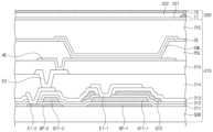
도 3은 도 2의 I-I'에 대응되는 예시적인 단면도이다. 도 3은 도 2의 화소(PX)에 대응되는 영역의 표시 유닛(210) 및 입력 감지 유닛(220)의 단면도일 수 있다. 도 3의 단면도는 예시적인 것으로 이해될 것이고, 화소(PX)에 대한 단면도의 형태는 단면의 위치에 따라 다를 수 있다. 예를 들어, 단면의 위치에 따라 컨택 홀의 위치, 패턴들 사이의 연결 관계, 절연층의 배치들이 달라질 수 있다.Fig. 3 is an exemplary cross-sectional view corresponding to I-I' of Fig. 2. Fig. 3 may be a cross-sectional view of a display unit (210) and an input detection unit (220) in an area corresponding to a pixel (PX) of Fig. 2. It should be understood that the cross-sectional view of Fig. 3 is exemplary, and the shape of the cross-sectional view for the pixel (PX) may vary depending on the position of the cross-section. For example, the position of a contact hole, the connection relationship between patterns, and the arrangement of an insulating layer may vary depending on the position of the cross-section.
도 3을 참조하면, 표시 유닛(210)은 베이스 기판(SUB), 발광 소자를 구동하기 위한 다양한 회로 소자들을 포함하는 회로 소자층, 발광 소자를 포함하는 표시 소자층, 및 봉지층(TFE)을 포함할 수 있다. 및 베이스 기판(SUB)은 절연 물질을 포함할 수 있다. 예를 들어, 베이스 기판(BS)은 폴리 이미드(Polyimide, PI)와 같은 벤딩 가능한 물질을 포함할 수 있다. 또는, 베이스 기판은 유리 또는 플라스틱과 같은 강성의 물질을 포함할 수 있다.Referring to FIG. 3, the display unit (210) may include a base substrate (SUB), a circuit element layer including various circuit elements for driving a light-emitting element, a display element layer including a light-emitting element, and an encapsulation layer (TFE). And the base substrate (SUB) may include an insulating material. For example, the base substrate (BS) may include a bendable material such as polyimide (PI). Alternatively, the base substrate may include a rigid material such as glass or plastic.
회로 소자층은 절연층들(211~215), 반도체 패턴들(SP-1, SP-2), 도전 패턴들(GT1-1, GT1-2, GT2), 연결 패턴들(E1-1, E1-2, E2)을 포함할 수 있다. 복수의 절연층들(211~215), 반도체 패턴들(SP-1, SP-2), 도전 패턴들(GT1-1, GT1-2, GT2), 연결 패턴들(E1-1, E1-2, E2)은 상술된 화소(PX)에 포함된 트랜지스터들 또는 커패시터를 형성하는데 이용된다. 도시되지 않았으나, 회로 소자층은 베이스 기판(SUB) 상에 배치되는 버퍼층을 더 포함할 수 있다. 버퍼층은 적어도 하나의 무기층을 포함할 수 있고, 베이스 기판(SUB)과 반도체 패턴들(SP-1, SP-2) 사이의 결합력을 향상시킬 수 있다.The circuit element layer may include insulating layers (211 to 215), semiconductor patterns (SP-1, SP-2), conductive patterns (GT1-1, GT1-2, GT2), and connection patterns (E1-1, E1-2, E2). The plurality of insulating layers (211 to 215), semiconductor patterns (SP-1, SP-2), conductive patterns (GT1-1, GT1-2, GT2), and connection patterns (E1-1, E1-2, E2) are used to form transistors or capacitors included in the pixel (PX) described above. Although not shown, the circuit element layer may further include a buffer layer disposed on the base substrate (SUB). The buffer layer may include at least one inorganic layer and may improve a bonding strength between the base substrate (SUB) and the semiconductor patterns (SP-1, SP-2).
반도체 패턴들(SP-1, SP-2)은 베이스 기판(SUB) (및 버퍼층(미도시)) 상에 배치된다. 반도체 패턴들(SP-1, SP-2)은 폴리실리콘을 포함할 수 있으나 이에 제한되지 않고, 비정질실리콘 또는 금속 산화물을 포함할 수도 있다. 반도체 패턴들(SP-1, SP-2)은 화소(PX)에 걸쳐 특정한 규칙을 갖도록 배열될 수 있다. 반도체 패턴들(SP-1, SP-2)은 도핑영역과 비-도핑영역을 포함할 수 있다. 도핑영역은 N형 도판트 또는 P형 도판트로 도핑될 수 있다. 일례로, P타입의 트랜지스터는 P형 도판트로 도핑된 도핑영역을 포함할 수 있다.Semiconductor patterns (SP-1, SP-2) are arranged on a base substrate (SUB) (and a buffer layer (not shown)). The semiconductor patterns (SP-1, SP-2) may include polysilicon, but are not limited thereto, and may also include amorphous silicon or a metal oxide. The semiconductor patterns (SP-1, SP-2) may be arranged to have a specific rule across the pixel (PX). The semiconductor patterns (SP-1, SP-2) may include a doped region and a non-doped region. The doped region may be doped with an N-type dopant or a P-type dopant. For example, a P-type transistor may include a doped region doped with a P-type dopant.
도핑영역의 전도성은 비-도핑영역보다 크고, 실질적으로 전극 또는 신호 라인의 역할을 가질 수 있다. 비-도핑영역은 실질적으로 트랜지스터의 액티브(또는 채널)에 대응될 수 있다. 다시 말해, 반도체 패턴들(SP-1, SP-2)의 일부분은 트랜지스터의 액티브일수 있고, 다른 일부분은 트랜지스터의 소스 또는 드레인일 수 있고, 또 다른 일부분은 연결전극 또는 연결 신호라인일 수 있다.The conductivity of the doped region is greater than that of the non-doped region, and can substantially play the role of an electrode or a signal line. The non-doped region can substantially correspond to the active (or channel) of the transistor. In other words, a part of the semiconductor patterns (SP-1, SP-2) can be the active part of the transistor, another part can be the source or drain of the transistor, and another part can be the connecting electrode or the connecting signal line.
제1 절연층(211)은 베이스 기판(SUB) (및 버퍼층(미도시)) 및 반도체 패턴들(SP-1, SP-2) 상에 배치된다. 제1 절연층(10)은 복수 개의 화소들(PX, 도 2 참조)에 공통으로 중첩하며, 반도체 패턴들(SP-1, SP-2)을 커버한다. 제1 절연층(211)은 무기층 및/또는 유기층일 수 있으며, 단층 또는 다층 구조를 가질 수 있다. 일례로, 제1 절연층(211)은 단층의 실리콘 옥사이드층일 수 있다. 다만, 이에 제한되지 않고, 제1 절연층(211)은 알루미늄 옥사이드, 티타늄 옥사이드, 실리콘 옥사이드, 실리콘 나이트라이드, 지르코늄옥사이드, 및 하프늄 옥사이드 중 적어도 하나를 포함할 수 있다.A first insulating layer (211) is disposed on a base substrate (SUB) (and a buffer layer (not shown)) and semiconductor patterns (SP-1, SP-2). The first insulating layer (10) overlaps a plurality of pixels (PX, see FIG. 2) in common and covers the semiconductor patterns (SP-1, SP-2). The first insulating layer (211) may be an inorganic layer and/or an organic layer and may have a single-layer or multi-layer structure. For example, the first insulating layer (211) may be a single-layer silicon oxide layer. However, the present invention is not limited thereto, and the first insulating layer (211) may include at least one of aluminum oxide, titanium oxide, silicon oxide, silicon nitride, zirconium oxide, and hafnium oxide.
제1 도전 패턴들(GT1-1, GT1-2)은 제1 절연층(211) 상에 배치된다. 제1 도전 패턴들(GT1-1, GT1-2)은 금속 패턴의 일부일 수 있다. 일례로, 제1 도전 패턴들(GT1-1, GT1-2)은 티타늄/알루미늄/티타늄의 3층 구조를 가질 수 있으나, 이에 제한되지 않는다. 제1 도전 패턴들(GT1-1, GT1-2)은 반도체 패턴들(SP-1, SP-2)에 각각 중첩한다. 제1 도전 패턴들(GT1-1, GT1-2)은 반도체 패턴들(SP-1, SP-2)에 흐르는 전류 등을 제어하는 게이트일 수 있다. 중첩한다. 반도체 패턴들(SP-1, SP-2)을 도핑하는 공정에서 제1 도전 패턴들(GT1-1, GT1-2)는 마스크와 같을 수 있다.The first conductive patterns (GT1-1, GT1-2) are arranged on the first insulating layer (211). The first conductive patterns (GT1-1, GT1-2) may be a part of a metal pattern. For example, the first conductive patterns (GT1-1, GT1-2) may have a three-layer structure of titanium/aluminum/titanium, but is not limited thereto. The first conductive patterns (GT1-1, GT1-2) overlap the semiconductor patterns (SP-1, SP-2), respectively. The first conductive patterns (GT1-1, GT1-2) may be gates that control current flowing in the semiconductor patterns (SP-1, SP-2), etc. overlap. In a process of doping the semiconductor patterns (SP-1, SP-2), the first conductive patterns (GT1-1, GT1-2) may be like a mask.
제2 절연층(212)은 제1 절연층(211) 및 제1 도전 패턴들(GT1-1, GT1-2) 상에 배치된다. 제2 절연층(212)은 복수 개의 화소들(PX, 도 2 참조)에 공통으로 중첩하며, 제1 도전 패턴들(GT1-1, GT1-2)을 커버한다. 제2 절연층(212)은 무기층 및/또는 유기층일 수 있으며, 단층 또는 다층 구조를 가질 수 있다. 일례로, 제2 절연층(212)은 단층의 실리콘 나이트라이드층일 수 있으나, 이에 제한되지 않는다.The second insulating layer (212) is disposed on the first insulating layer (211) and the first conductive patterns (GT1-1, GT1-2). The second insulating layer (212) overlaps a plurality of pixels (PX, see FIG. 2) in common and covers the first conductive patterns (GT1-1, GT1-2). The second insulating layer (212) may be an inorganic layer and/or an organic layer and may have a single-layer or multi-layer structure. For example, the second insulating layer (212) may be a single-layer silicon nitride layer, but is not limited thereto.
제2 도전 패턴(GT2)은 제2 절연층(212) 상에 배치된다. 제2 도전 패턴(GT2)은 제1 도전 패턴들(GT1-1, GT1-2) 중 적어도 하나(GT1-1)와 중첩하여, 도 2에서 설명된 커패시터를 정의할 수 있다. 이 경우, 제2 절연층(212)은 커패시터의 유전체일 수 있고, 제1 및 제2 도전 패턴들(GT1-1, GT2)은 커패시터의 전극들일 수 있다. 제2 도전 패턴(GT2)은 금속 패턴의 일부일 수 있다. 일례로, 제2 도전 패턴(GT2)은 티타늄/알루미늄/티타늄의 3층 구조를 가질 수 있으나, 이에 제한되지 않는다.The second conductive pattern (GT2) is disposed on the second insulating layer (212). The second conductive pattern (GT2) may overlap at least one (GT1-1) of the first conductive patterns (GT1-1, GT1-2) to define the capacitor described in FIG. 2. In this case, the second insulating layer (212) may be a dielectric of the capacitor, and the first and second conductive patterns (GT1-1, GT2) may be electrodes of the capacitor. The second conductive pattern (GT2) may be a part of a metal pattern. For example, the second conductive pattern (GT2) may have a three-layer structure of titanium/aluminum/titanium, but is not limited thereto.
제3 절연층(213)은 제2 절연층(212) 및 제2 도전 패턴(GT2) 상에 배치된다. 제3 절연층(213)은 복수 개의 화소들(PX, 도 2 참조)에 공통으로 중첩하며, 제2 도전 패턴(GT2)을 커버한다. 제3 절연층(213)은 무기층 및/또는 유기층일 수 있으며, 단층 또는 다층 구조를 가질 수 있다. 일례로, 제3 절연층(213)은 실리콘 옥사이드층 및 실리콘 나이트라이드층을 포함할 수 있으나, 이에 제한되지 않는다.The third insulating layer (213) is disposed on the second insulating layer (212) and the second conductive pattern (GT2). The third insulating layer (213) overlaps a plurality of pixels (PX, see FIG. 2) in common and covers the second conductive pattern (GT2). The third insulating layer (213) may be an inorganic layer and/or an organic layer and may have a single-layer or multi-layer structure. For example, the third insulating layer (213) may include a silicon oxide layer and a silicon nitride layer, but is not limited thereto.
중간 연결 패턴들(E1-1, E1-2)은 제1 내지 제3 절연층들(211~213) 중 적어도 하나를 관통하여 반도체 패턴들(SP-1, SP-2) 또는 도전 패턴들(GT1-1, GT1-2, GT2) 중 적어도 하나와 연결될 수 있다. 제1 내지 제3 절연층들(211~213) 중 적어도 하나를 관통하도록, 컨택 홀들이 형성될 수 있고, 컨택 홀들을 통하여 중간 연결 패턴들(E1-1, E1-2) 각각은 해당 반도체 패턴 또는 도전 패턴에 연결될 수 있다. 예를 들어, 중간 연결 패턴들(E1-1, E1-2) 중 어느 하나(E1-1)는 게이트 신호를 게이트에 전달하도록 제1 도전 패턴(GT1-1)에 연결될 수 있다. 예를 들어, 중간 연결 패턴들(E1-1, E1-2) 중 다른 하나(E1-2)는 반도체 패턴(SP-2)의 드레인 (또는 소스)에 연결되어 트랜지스터에 흐르는 전류를 다른 전자 소자로 전달할 수 있다. 일례로, 중간 연결 패턴들(E1-1, E1-2)은 티타늄/알루미늄/티타늄의 3층 구조를 가질 수 있으나, 이에 제한되지 않는다.The intermediate connection patterns (E1-1, E1-2) can be connected to at least one of the semiconductor patterns (SP-1, SP-2) or the conductive patterns (GT1-1, GT1-2, GT2) by penetrating at least one of the first to third insulating layers (211 to 213). Contact holes can be formed to penetrate at least one of the first to third insulating layers (211 to 213), and each of the intermediate connection patterns (E1-1, E1-2) can be connected to the corresponding semiconductor pattern or conductive pattern through the contact holes. For example, one (E1-1) of the intermediate connection patterns (E1-1, E1-2) can be connected to the first conductive pattern (GT1-1) to transmit a gate signal to the gate. For example, another one (E1-2) of the intermediate connection patterns (E1-1, E1-2) may be connected to the drain (or source) of the semiconductor pattern (SP-2) to transmit current flowing in the transistor to another electronic element. For example, the intermediate connection patterns (E1-1, E1-2) may have a three-layer structure of titanium/aluminum/titanium, but is not limited thereto.
제4 절연층(214)은 제3 절연층(213) 및 중간 연결 패턴들(E1-1, E1-2) 상에 배치된다. 제4 절연층(214)은 복수 개의 화소들(PX, 도 2 참조)에 공통으로 중첩하며, 중간 연결 패턴들(E1-1, E1-2)을 커버한다. 제4 절연층(214)은 유기층일 수 있다. 제4 절연층(214)은 평탄면을 제공할 수 있다.The fourth insulating layer (214) is disposed on the third insulating layer (213) and the intermediate connecting patterns (E1-1, E1-2). The fourth insulating layer (214) overlaps a plurality of pixels (PX, see FIG. 2) in common and covers the intermediate connecting patterns (E1-1, E1-2). The fourth insulating layer (214) may be an organic layer. The fourth insulating layer (214) may provide a flat surface.
상부 연결 패턴(E2)은 제4 절연층(214)을 관통하여 중간 연결 패턴들(E1-1, E1-2) 중 적어도 하나와 연결될 수 있다. 제4 절연층(214)을 관통하도록, 컨택 홀이 형성될 수 있다. 예를 들어, 상부 연결 패턴(E2)은 전류를 발광 소자에 전달하도록 중간 연결 패턴(E1-2)에 연결될 수 있다. 일례로, 상부 연결 패턴(E2)은 티타늄/알루미늄/티타늄의 3층 구조를 가질 수 있으나, 이에 제한되지 않는다.The upper connection pattern (E2) can be connected to at least one of the intermediate connection patterns (E1-1, E1-2) by penetrating the fourth insulating layer (214). A contact hole can be formed to penetrate the fourth insulating layer (214). For example, the upper connection pattern (E2) can be connected to the intermediate connection pattern (E1-2) to transmit current to the light-emitting element. For example, the upper connection pattern (E2) can have a three-layer structure of titanium/aluminum/titanium, but is not limited thereto.
제5 절연층(215)은 제4 절연층(214) 및 상부 연결 패턴(E2) 상에 배치된다. 제5 절연층(215)은 복수 개의 화소들(PX, 도 2 참조)에 공통으로 중첩하며, 상부 연결 패턴(E2)을 커버한다. 제5 절연층(215)은 유기층일 수 있다. 제5 절연층(215)은 평탄면을 제공할 수 있다. 제5 절연층(215)에 컨택 홀이 형성될 수 있고, 컨택 홀을 통하여 상부 연결 패턴(E2)은 표시 소자층에 전기 신호를 전달할 수 있다.The fifth insulating layer (215) is disposed on the fourth insulating layer (214) and the upper connecting pattern (E2). The fifth insulating layer (215) overlaps a plurality of pixels (PX, see FIG. 2) in common and covers the upper connecting pattern (E2). The fifth insulating layer (215) may be an organic layer. The fifth insulating layer (215) may provide a flat surface. A contact hole may be formed in the fifth insulating layer (215), and the upper connecting pattern (E2) may transmit an electric signal to the display element layer through the contact hole.
표시 소자층은 제1 전극(AE), 발광층(EML), 제2 전극(CE), 및 화소 정의막(PDL)을 포함할 수 있다. 제1 전극(AE), 발광층(EML), 및 제2 전극(CE)은 발광 소자를 정의할 수 있다. 도시되지 않았으나, 제1 전극(AE) 및 발광층(EML) 사이에 정공 제어층이 배치될 수 있고, 제2 전극(CE) 및 발광층(EML) 사이에 전자 제어층이 배치될 수 있다.The display element layer may include a first electrode (AE), an emission layer (EML), a second electrode (CE), and a pixel defining layer (PDL). The first electrode (AE), the emission layer (EML), and the second electrode (CE) may define a light emitting element. Although not shown, a hole control layer may be disposed between the first electrode (AE) and the emission layer (EML), and an electron control layer may be disposed between the second electrode (CE) and the emission layer (EML).
제1 전극(AE)은 제5 절연층(215) 및 상부 연결 패턴(E2) 상에 배치된다. 제1 전극(AE)은 제5 절연층(215)을 관통하여 상부 연결 패턴(E2)에 연결될 수 있다. 제1 전극(AE)은 발광 소자의 아노드 전극일 수 있다. 제1 전극(AE)은 상부 연결 패턴(E2)으로부터 전기 신호를 수신할 수 있다.The first electrode (AE) is disposed on the fifth insulating layer (215) and the upper connecting pattern (E2). The first electrode (AE) can penetrate the fifth insulating layer (215) and be connected to the upper connecting pattern (E2). The first electrode (AE) can be an anode electrode of a light-emitting element. The first electrode (AE) can receive an electric signal from the upper connecting pattern (E2).
화소 정의막(PDL)은 제5 절연층(215) 및 제1 전극(AE) 상에 배치된다. 화소 정의막(PDL)은 발광 영역에 중첩하는 개구부를 정의할 수 있다. 이러한 개구부는 제1 전극(AE)의 일부를 노출시킬 수 있다.A pixel defining layer (PDL) is disposed on the fifth insulating layer (215) and the first electrode (AE). The pixel defining layer (PDL) can define an opening that overlaps the light-emitting area. This opening can expose a portion of the first electrode (AE).
발광층(EML)은 화소 정의막(PDL)에 의하여 정의되는 개구부에 배치되고, 제1 전극(AE) 상에 배치된다. 발광층(EML)은 유기발광물질을 포함할 수 있으나, 이에 제한되지 않고, 양자점 또는 양자로드 등을 포함할 수 있다. 발광층(EML)은 발광 물질을 포함할 수 있다. 예를 들어, 발광층(EML)은 적색, 녹색, 및 청색을 발광하는 물질들 중 적어도 어느 하나의 물질을 포함할 수 있다. 발광층(EML)은 제1 전극(AE) 및 제2 전극(CE) 사이의 전위 차이에 기초하여 발광될 수 있다.An emission layer (EML) is disposed in an opening defined by a pixel defining layer (PDL) and is disposed on a first electrode (AE). The emission layer (EML) may include an organic light-emitting material, but is not limited thereto, and may include quantum dots or quantum rods, etc. The emission layer (EML) may include a light-emitting material. For example, the emission layer (EML) may include at least one material that emits red, green, and blue. The emission layer (EML) may emit light based on a potential difference between the first electrode (AE) and the second electrode (CE).
제2 전극(CE)은 발광층(EML) 및 화소 정의막(PDL) 상에 배치된다. 제2 전극(CE)은 광이 용이하게 출사되도록, 투과성 도전 물질 또는 반 투과성 도전 물질을 포함할 수 있다. 제2 전극(CE)은 복수 개의 화소들(PX, 도 2 참조)에 공통으로 중첩하여 배치될 수 있다.The second electrode (CE) is disposed on the emission layer (EML) and the pixel defining layer (PDL). The second electrode (CE) may include a transparent conductive material or a semi-transparent conductive material so that light can be easily emitted. The second electrode (CE) may be disposed so as to overlap a plurality of pixels (PX, see FIG. 2).
봉지층(TFE)은 제2 전극(CE) 상에 배치되고, 표시 소자층을 커버한다. 봉지층(TFE)은 무기층 및/또는 유기층일 수 있으며, 단층 또는 다층 구조를 가질 수 있다. 봉지층(TFE)은 평탄면을 제공할 수 있다.The encapsulation layer (TFE) is disposed on the second electrode (CE) and covers the display element layer. The encapsulation layer (TFE) may be an inorganic layer and/or an organic layer, and may have a single-layer or multi-layer structure. The encapsulation layer (TFE) may provide a flat surface.
입력 감지 유닛(220)은 절연층들(221, 222) 및 도전층들(T1, T2)을 포함할 수 있다. 입력 감지 유닛(220)은 표시 유닛(210) 상에 배치될 수 있다.The input detection unit (220) may include insulating layers (221, 222) and conductive layers (T1, T2). The input detection unit (220) may be placed on the display unit (210).
제6 절연층(221)은 표시 유닛(210)의 봉지층(TFE) 상에 배치된다. 제6 절연층(221)은 무기층 및/또는 유기층일 수 있으며, 단층 또는 다층 구조를 가질 수 있다. 일례로, 제6 절연층(221)은 단층의 실리콘 나이트라이드층일 수 있으나, 이에 제한되지 않는다.The sixth insulating layer (221) is disposed on the encapsulating layer (TFE) of the display unit (210). The sixth insulating layer (221) may be an inorganic layer and/or an organic layer, and may have a single-layer or multi-layer structure. For example, the sixth insulating layer (221) may be a single-layer silicon nitride layer, but is not limited thereto.
제1 도전층(T1)은 제6 절연층(221) 상에 배치된다. 예를 들어, 제1 도전층(T1)은 도 2의 제1 연결 패턴들(BP1) 또는 제2 연결 패턴들(BP2) 중 하나를 포함할 수 있다. 제1 도전층(T1)은 컨택 홀을 통하여 제2 도전층(T2)과 연결될 수 있다. 제1 도전층(T1)은 ITO(indium tin oxide), IZO(indium zinc oxide), ZnO(zinc oxide), ITZO(indium tin zinc oxide), PEDOT, 금속 나노 와이어, 그라핀 등의 투명 도전층, 및 몰리브덴, 은, 티타늄, 구리, 알루미늄, 및 이들의 합금과 같은 금속층들 중 적어도 2이상을 포함할 수 있다. 일례로, 제1 도전층(T1)은 티타늄/알루미늄/티타늄의 3층 구조를 가질 수 있다.The first conductive layer (T1) is disposed on the sixth insulating layer (221). For example, the first conductive layer (T1) may include one of the first connection patterns (BP1) or the second connection patterns (BP2) of FIG. 2. The first conductive layer (T1) may be connected to the second conductive layer (T2) through a contact hole. The first conductive layer (T1) may include at least two or more of transparent conductive layers such as ITO (indium tin oxide), IZO (indium zinc oxide), ZnO (zinc oxide), ITZO (indium tin zinc oxide), PEDOT, metal nanowires, graphene, and metal layers such as molybdenum, silver, titanium, copper, aluminum, and alloys thereof. For example, the first conductive layer (T1) may have a three-layer structure of titanium/aluminum/titanium.
제7 절연층(222)은 제6 절연층(221) 및 제1 도전층(T1) 상에 배치된다. 제7 절연층(222)은 제1 도전층(T1)을 커버한다. 제7 절연층(222)은 무기층 및/또는 유기층일 수 있으며, 단층 또는 다층 구조를 가질 수 있다. 일례로, 제7 절연층(222)은 단층의 실리콘 나이트라이드층일 수 있으나, 이에 제한되지 않는다.The seventh insulating layer (222) is disposed on the sixth insulating layer (221) and the first conductive layer (T1). The seventh insulating layer (222) covers the first conductive layer (T1). The seventh insulating layer (222) may be an inorganic layer and/or an organic layer, and may have a single-layer or multi-layer structure. For example, the seventh insulating layer (222) may be a single-layer silicon nitride layer, but is not limited thereto.
제2 도전층(T2)은 제7 절연층(222) 상에 배치된다. 제2 도전층(T2)은 제7 절연층(222)을 관통하여 제1 도전층(T1)과 연결될 수 있다. 제2 도전층(T2)은 도 2의 제1 연결 패턴들(BP1) 또는 제2 연결 패턴들(BP2) 중 하나, 및 제1 감지 패턴들(SP1) 및 제2 감지 패턴들(SP2)을 포함할 수 있다. 제2 도전층(T2)은 ITO(indium tin oxide), IZO(indium zinc oxide), ZnO(zinc oxide), ITZO(indium tin zinc oxide), PEDOT, 금속 나노 와이어, 그라핀 등의 투명 도전층, 및 몰리브덴, 은, 티타늄, 구리, 알루미늄, 및 이들의 합금과 같은 금속층들 중 적어도 2이상을 포함할 수 있다. 일례로, 제2 도전층(T2)은 티타늄/알루미늄/티타늄의 3층 구조를 가질 수 있다.The second conductive layer (T2) is disposed on the seventh insulating layer (222). The second conductive layer (T2) may be connected to the first conductive layer (T1) by penetrating the seventh insulating layer (222). The second conductive layer (T2) may include one of the first connection patterns (BP1) or the second connection patterns (BP2) of FIG. 2, and the first sensing patterns (SP1) and the second sensing patterns (SP2). The second conductive layer (T2) may include at least two or more of transparent conductive layers such as ITO (indium tin oxide), IZO (indium zinc oxide), ZnO (zinc oxide), ITZO (indium tin zinc oxide), PEDOT, metal nanowires, graphene, and metal layers such as molybdenum, silver, titanium, copper, aluminum, and alloys thereof. For example, the second conductive layer (T2) may have a three-layer structure of titanium/aluminum/titanium.
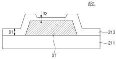
도 4는 본 발명의 일 실시예에 따른 도 2의 II-II'에 대응되는 단면도이다. 도 4는 도 2의 패드들(PD)에 대응되는 영역의 단면도일 수 있다. 도 4를 참조하면, 패드들(PD)에 대응되는 영역에서, 도 2의 전자 패널(200)은 베이스 기판(SUB), 복수의 절연층들(211, 212, 213, 221, 222) 및 신호 라인(GT) 및 패드 도전 패턴(TT)를 포함한다.FIG. 4 is a cross-sectional view corresponding to II-II' of FIG. 2 according to one embodiment of the present invention. FIG. 4 may be a cross-sectional view of an area corresponding to pads (PD) of FIG. 2. Referring to FIG. 4, in an area corresponding to pads (PD), the electronic panel (200) of FIG. 2 includes a base substrate (SUB), a plurality of insulating layers (211, 212, 213, 221, 222), a signal line (GT), and a pad conductive pattern (TT).
복수의 절연층들(211, 212, 213, 221, 222)은 베이스 기판(SUB) 상에 배치되고, 적층된다. 도 4의 절연층들 각각의 도면 부호는 도 3의 절연층에 대응된다. 즉, 도 4에 도시된 복수의 절연층들(211, 212, 213, 221, 222) 각각은 도 3의 제1 절연층(211), 제2 절연층(212), 제3 절연층(213), 제6 절연층(221), 및 제7 절연층(222)과 함께 생성된다. 이하에서, 도 3과의 일관된 설명을 위하여, 복수의 절연층들 각각의 명칭은 도 3의 도면 부호와 연관되어 정의될 것이다. 예를 들어, 도 4에 도시된 5개의 절연층들이 제1 내지 제5 절연층들로 설명되지 않고, 도 3의 도면 부호에 대응되는 명칭에 맞게 설명될 것이다.A plurality of insulating layers (211, 212, 213, 221, 222) are arranged and laminated on a base substrate (SUB). The drawing reference numerals of each of the insulating layers in FIG. 4 correspond to the insulating layers in FIG. 3. That is, each of the plurality of insulating layers (211, 212, 213, 221, 222) illustrated in FIG. 4 is generated together with the first insulating layer (211), the second insulating layer (212), the third insulating layer (213), the sixth insulating layer (221), and the seventh insulating layer (222) in FIG. 3. Hereinafter, for consistent description with FIG. 3, the names of each of the plurality of insulating layers will be defined in relation to the drawing reference numerals of FIG. 3. For example, the five insulating layers illustrated in FIG. 4 will not be described as the first to fifth insulating layers, but will be described according to the names corresponding to the drawing reference numerals of FIG. 3.
제1 절연층(211)은 베이스 기판(SUB) 상에 배치된다. 제1 절연층(211)은 도 3의 표시 유닛(210)에서 반도체 패턴들(SP-1, SP-2)을 커버하기 위하여 제1 절연층(211)을 형성할 때, 함께 형성될 수 있다. 따라서, 제1 절연층(211)은 도 3의 제1 절연층(211)에 대응되는 물질을 포함하며, 실질적으로 동일한 두께를 가질 수 있다.The first insulating layer (211) is arranged on the base substrate (SUB). The first insulating layer (211) may be formed together with the first insulating layer (211) when forming the first insulating layer (211) to cover the semiconductor patterns (SP-1, SP-2) in the display unit (210) of FIG. 3. Accordingly, the first insulating layer (211) includes a material corresponding to the first insulating layer (211) of FIG. 3 and may have substantially the same thickness.
신호 라인(GT)은 제1 절연층(211) 상에 배치된다. 신호 라인(GT)은 도 3의 게이트에 대응되는 제1 도전 패턴들(GT1-1, GT1-2)을 형성할 때, 함께 형성될 수 있다. 따라서, 신호 라인(GT)은 도 3의 제1 도전 패턴들(GT1-1, GT1-2)에 대응되는 물질을 포함하며, 실질적으로 동일한 두께를 가질 수 있다.The signal line (GT) is arranged on the first insulating layer (211). The signal line (GT) can be formed together with the first conductive patterns (GT1-1, GT1-2) corresponding to the gate of Fig. 3. Accordingly, the signal line (GT) includes a material corresponding to the first conductive patterns (GT1-1, GT1-2) of Fig. 3 and can have substantially the same thickness.
제2 절연층(212)은 신호 라인(GT) 및 제1 절연층(211) 상에 배치된다. 제2 절연층(212)은 신호 라인(GT)을 커버한다. 제2 절연층(212)은 도 3에서 제1 도전 패턴들(GT1-1, GT1-2)을 커버하기 위하여 제2 절연층(212)을 형성할 때, 함께 형성될 수 있다. 따라서, 제2 절연층(212)은 도 3의 제2 절연층(212)에 대응되는 물질을 포함하며, 실질적으로 동일한 두께를 가질 수 있다.The second insulating layer (212) is disposed on the signal line (GT) and the first insulating layer (211). The second insulating layer (212) covers the signal line (GT). The second insulating layer (212) may be formed together with the second insulating layer (212) when forming the second insulating layer (212) to cover the first conductive patterns (GT1-1, GT1-2) in FIG. 3. Accordingly, the second insulating layer (212) includes a material corresponding to the second insulating layer (212) of FIG. 3 and may have substantially the same thickness.
제3 절연층(213)은 제2 절연층(212) 상에 배치된다. 제3 절연층(213)은 도 3에서 제2 도전 패턴(GT2)을 커버하기 위하여 제3 절연층(213)을 형성할 때, 함께 형성될 수 있다. 따라서, 제3 절연층(213)은 도 3의 제3 절연층(213)에 대응되는 물질을 포함하며, 실질적으로 동일한 두께를 가질 수 있다. 도시된 바와 달리, 제2 절연층(212) 및 제3 절연층(213) 중 하나는 해당 영역에 배치되지 않을 수 있다.The third insulating layer (213) is disposed on the second insulating layer (212). The third insulating layer (213) may be formed together with the third insulating layer (213) when forming the third insulating layer (213) to cover the second conductive pattern (GT2) in FIG. 3. Accordingly, the third insulating layer (213) includes a material corresponding to the third insulating layer (213) of FIG. 3 and may have substantially the same thickness. Unlike as illustrated, one of the second insulating layer (212) and the third insulating layer (213) may not be disposed in the corresponding area.
제2 절연층(212) 및 제3 절연층(213)은 도 3의 표시 유닛(210)의 공정이 완료될 때까지 신호 라인(GT)이 외부에 노출되지 않도록, 신호 라인(GT)을 커버할 수 있다. 신호 라인(GT)이 외부에 노출되는 경우, 표시 유닛(210)의 공정을 위한 에칭 과정에서 신호 라인(GT)과 에칭액이 반응할 수 있고, 금속 입자가 생성될 수 있다. 이 경우, 패드 영역에 단락 등이 발생될 수 있다. 예를 들어, 신호 라인(GT)이 알루미늄을 포함하는 경우, 표시 소자층의 공정에 사용되는 에칭액에 포함된 은이 알루미늄에 의하여 환원될 수 있다. 은 입자는 신호 라인(GT) 주변에 발생하여 도전 패턴들 또는 신호 라인 사이의 단락을 유발시킬 수 있다. 제2 절연층(212) 및 제3 절연층(213)은 이러한 화학 반응이 발생하지 않도록 신호 라인(GT)을 커버할 수 있다.The second insulating layer (212) and the third insulating layer (213) can cover the signal line (GT) so that the signal line (GT) is not exposed to the outside until the process of the display unit (210) of FIG. 3 is completed. When the signal line (GT) is exposed to the outside, the signal line (GT) and the etching solution may react during the etching process for the process of the display unit (210), and metal particles may be generated. In this case, a short circuit, etc. may occur in the pad area. For example, when the signal line (GT) includes aluminum, silver included in the etching solution used in the process of the display element layer may be reduced by aluminum. The silver particles may be generated around the signal line (GT) and cause a short circuit between the conductive patterns or the signal line. The second insulating layer (212) and the third insulating layer (213) can cover the signal line (GT) so that such a chemical reaction does not occur.
패드들(PD)은 도 3의 연결 패턴들(E1-1, E1-2, E2)에 대응되는 도전 패턴을 포함하지 않을 수 있다. 도 3을 참조하면, 중간 연결 패턴들(E1-1, E1-2, E2)을 커버하는 절연층은 표시 유닛(210)에 포함되지 않고, 평탄면을 제공하는 제4 절연층(214)이 중간 연결 패턴들(E1-1, E1-2, E2)을 커버한다. 이에 따라, 연결 패턴들(E1-1, E1-2, E2)에 대응되는 도전 패턴이 신호 라인(GT)의 말단에 형성되는 경우, 표시 소자층의 공정 시에 도전 패턴이 외부에 노출되어 패드들(PD)의 품질이 감소할 수 있다. 연결 패턴들(E1-1, E1-2, E2)을 형성할 때, 제1 내지 제3 절연층들(211~213) 정도의 두께의 절연층이 이용되지 않기 때문이다.The pads (PD) may not include a conductive pattern corresponding to the connection patterns (E1-1, E1-2, E2) of FIG. 3. Referring to FIG. 3, an insulating layer covering the intermediate connection patterns (E1-1, E1-2, E2) is not included in the display unit (210), and a fourth insulating layer (214) providing a flat surface covers the intermediate connection patterns (E1-1, E1-2, E2). Accordingly, when the conductive pattern corresponding to the connection patterns (E1-1, E1-2, E2) is formed at the end of the signal line (GT), the conductive pattern may be exposed to the outside during the process of the display element layer, which may reduce the quality of the pads (PD). This is because an insulating layer having a thickness similar to that of the first to third insulating layers (211 to 213) is not used when forming the connection patterns (E1-1, E1-2, E2).
제6 절연층(221)은 제3 절연층(213) 상에 배치된다. 제6 절연층(221)은 도 3에서 표시 유닛(210) 상에 제6 절연층(221)을 형성할 때, 함께 형성될 수 있다. 즉, 제6 절연층(221)은 입력 감지 유닛(220)의 공정 시에 생성될 수 있다. 따라서, 제6 절연층(221)은 도 3의 제6 절연층(221)에 대응되는 물질을 포함하며, 실질적으로 동일한 두께를 가질 수 있다.The sixth insulating layer (221) is disposed on the third insulating layer (213). The sixth insulating layer (221) may be formed together with the sixth insulating layer (221) when forming the sixth insulating layer (221) on the display unit (210) in FIG. 3. That is, the sixth insulating layer (221) may be generated during the process of the input detection unit (220). Accordingly, the sixth insulating layer (221) includes a material corresponding to the sixth insulating layer (221) of FIG. 3 and may have substantially the same thickness.
제7 절연층(222)은 제6 절연층(221) 상에 배치된다. 제7 절연층(222)은 도 3에서 제1 도전층(T1)을 커버하기 위하여 제7 절연층(222)을 형성할 때, 함께 형성될 수 있다. 즉, 제7 절연층(222)은 입력 감지 유닛(220)의 공정 시에 생성될 수 있다. 따라서, 제7 절연층(222)은 도 3의 제7 절연층(222)에 대응되는 물질을 포함하며, 실질적으로 동일한 두께를 가질 수 있다.The seventh insulating layer (222) is disposed on the sixth insulating layer (221). The seventh insulating layer (222) may be formed together with the seventh insulating layer (222) when forming the seventh insulating layer (222) to cover the first conductive layer (T1) in FIG. 3. That is, the seventh insulating layer (222) may be generated during the process of the input detection unit (220). Accordingly, the seventh insulating layer (222) includes a material corresponding to the seventh insulating layer (222) of FIG. 3 and may have substantially the same thickness.
패드 도전 패턴(TT)은 제2 절연층(212), 제3 절연층(213), 제6 절연층(221), 및 제7 절연층(222)을 관통하여 신호 라인(GT)의 말단과 연결될 수 있다. 도 2의 패드들(PD) 각각은 패드 도전 패턴(TT)을 포함한다. 해당 절연층들을 관통하도록, 컨택 홀이 형성될 수 있고, 이러한 컨택 홀은 도 3의 제1 도전층(T1) 및 제2 도전층(T2)을 연결하기 위한 컨택 홀을 형성할 때, 함께 형성될 수 있다. 그리고, 패드 도전 패턴(TT)은 도 3의 제2 도전층(T2)을 형성할 때, 함께 형성될 수 있다. 따라서, 패드 도전 패턴(TT)은 도 3의 제2 도전층(T2)에 대응되는 물질을 포함할 수 있다. 또한, 입력 감지 유닛(220)의 공정 시에 외부에 패드들의 도전 패턴이 노출될 수 있다.The pad conductive pattern (TT) may be connected to the end of the signal line (GT) by penetrating the second insulating layer (212), the third insulating layer (213), the sixth insulating layer (221), and the seventh insulating layer (222). Each of the pads (PD) of FIG. 2 includes the pad conductive pattern (TT). A contact hole may be formed to penetrate the corresponding insulating layers, and this contact hole may be formed together when forming a contact hole for connecting the first conductive layer (T1) and the second conductive layer (T2) of FIG. 3. In addition, the pad conductive pattern (TT) may be formed together when forming the second conductive layer (T2) of FIG. 3. Therefore, the pad conductive pattern (TT) may include a material corresponding to the second conductive layer (T2) of FIG. 3. In addition, the conductive patterns of the pads may be exposed to the outside during the process of the input detection unit (220).
패드 도전 패턴(TT)은 도 2의 회로 기판(300)과 전기적으로 연결될 수 있다. 회로 기판(300)은 COP(Chip On Panel) 방식으로 전자 패널(200)에 접속될 수 있다. 이 경우, 패드들(PD) (패드 도전 패턴(TT)) 주위를 둘러싸는 유기막이 배치되지 않을 수 있다. 예를 들어, 유기막은 도 3의 제5 절연층(215)을 형성할 때, 함께 형성될 수 있다. 회로 기판(300)이 전자 패널(200) 상에 패드들(PD)을 통하여 접속되는 경우, COF(Chip On Film) 방식에 비하여, 패드들(PD)이 더 강한 압력을 받는다. 이러한 압력은 패드들(PD) 주위를 둘러싸는 유기막을 들뜨게 한다. 따라서, 유기막이 패드들(PD)을 둘러싸지 않을 수 있다.The pad conductive pattern (TT) may be electrically connected to the circuit board (300) of FIG. 2. The circuit board (300) may be connected to the electronic panel (200) in a COP (Chip On Panel) manner. In this case, an organic film surrounding the pads (PD) (pad conductive pattern (TT)) may not be disposed. For example, the organic film may be formed together when the fifth insulating layer (215) of FIG. 3 is formed. When the circuit board (300) is connected to the electronic panel (200) through the pads (PD), the pads (PD) are subjected to stronger pressure than in the COF (Chip On Film) manner. This pressure lifts the organic film surrounding the pads (PD). Therefore, the organic film may not surround the pads (PD).
도 5a 및 도 5c는 도 4에서 설명된 패드들을 제조하는 방법을 설명하기 위한 단면도이다.FIGS. 5A and 5C are cross-sectional views illustrating a method for manufacturing the pads described in FIG. 4.
도 5a를 참조하면, 베이스 기판(SUB) 상에 제1 절연층(211)이 배치된다. 제1 절연층(211)은 도 3의 제1 절연층(211)에 대응되며, 함께 형성된다. 그리고, 제1 절연층(211) 상에 신호 라인(GT)이 배치된다. 신호 라인(GT)은 도 3의 제1 도전 패턴들(GT1-1, GT1-2)을 형성할 때, 함께 형성된다.Referring to FIG. 5a, a first insulating layer (211) is disposed on a base substrate (SUB). The first insulating layer (211) corresponds to the first insulating layer (211) of FIG. 3 and is formed together with it. Then, a signal line (GT) is disposed on the first insulating layer (211). The signal line (GT) is formed together when forming the first conductive patterns (GT1-1, GT1-2) of FIG. 3.
이후에, 제2 절연층(212) 및 제3 절연층(213)이 신호 라인(GT)을 커버하도록, 신호 라인(GT) 상에 배치된다. 제2 절연층(212)은 도 3의 제2 절연층(212)에 대응되며, 함께 형성된다. 제3 절연층(213)은 도 3의 제3 절연층(213)에 대응되며, 함께 형성된다. 제3 절연층(213)이 형성된 이후에, 표시 유닛(210)의 공정이 완료될 때까지 신호 라인(GT)의 말단은 외부에 노출되지 않을 수 있다. 따라서, 표시 소자층의 공정 시에 에칭액에 따른 패드들(PD)의 품질 저하가 방지될 수 있다.Thereafter, a second insulating layer (212) and a third insulating layer (213) are placed on the signal line (GT) to cover the signal line (GT). The second insulating layer (212) corresponds to the second insulating layer (212) of FIG. 3 and is formed together with it. The third insulating layer (213) corresponds to the third insulating layer (213) of FIG. 3 and is formed together with it. After the third insulating layer (213) is formed, the end of the signal line (GT) may not be exposed to the outside until the process of the display unit (210) is completed. Therefore, the quality deterioration of the pads (PD) due to the etching solution during the process of the display element layer can be prevented.
도 5b를 참조하면, 제3 절연층(213) 상에 제6 절연층(221) 및 제7 절연층(222)이 배치된다. 제6 절연층(221) 및 제7 절연층(222)은 입력 감지 유닛(220)의 공정 시에 배치될 수 있다. 제6 절연층(221)은 도 3의 제6 절연층(221)에 대응되며, 함께 형성된다. 제7 절연층(222)은 도 3의 제7 절연층(222)에 대응되며, 함께 형성된다.Referring to FIG. 5b, a sixth insulating layer (221) and a seventh insulating layer (222) are disposed on a third insulating layer (213). The sixth insulating layer (221) and the seventh insulating layer (222) can be disposed during the process of the input detection unit (220). The sixth insulating layer (221) corresponds to the sixth insulating layer (221) of FIG. 3 and is formed together. The seventh insulating layer (222) corresponds to the seventh insulating layer (222) of FIG. 3 and is formed together.
도 5c를 참조하면, 패드 도전 패턴(TT)을 형성하기 위하여, 절연층들이 관통되도록 컨택 홀(CH)이 형성될 수 있다. 컨택 홀(CH)은 도 3의 제1 도전층(T1) 및 제2 도전층(T2)을 연결하기 위한 컨택 홀을 형성할 때, 함께 형성될 수 있다. 마스크를 통하여, 제2 절연층(212), 제3 절연층(213), 제6 절연층(221), 및 제7 절연층(222)의 일부 영역이 일괄적으로 에칭될 수 있다. 이후, 패드 도전 패턴(TT)이 신호 라인(GT)의 말단에 접속될 수 있다.Referring to FIG. 5c, in order to form a pad conductive pattern (TT), a contact hole (CH) may be formed so that the insulating layers penetrate. The contact hole (CH) may be formed together when forming a contact hole for connecting the first conductive layer (T1) and the second conductive layer (T2) of FIG. 3. Through a mask, some areas of the second insulating layer (212), the third insulating layer (213), the sixth insulating layer (221), and the seventh insulating layer (222) may be etched at once. Thereafter, the pad conductive pattern (TT) may be connected to the end of the signal line (GT).
상술된 공정에 의하여, 신호 라인(GT)의 말단 및 패드 도전 패턴(TT) 사이에 배치되는 절연층들 (이하, 패드 절연층)의 최대 두께가 결정될 수 있다. 패드 절연층의 최대 두께는 표시 유닛(210)에 포함되는 트랜지스터 또는 커패시터(회로 소자들)을 형성하거나 커버하는데 이용되는 하나의 절연층 (예를 들어, 제2 절연층(212) 또는 제3 절연층(213))의 두께 및 입력 감지 유닛(220)의 제1 및 제2 도전층들(T1, T2)을 연결하기 위한 컨택 홀의 두께의 합보다 클 수 있다. 패드 절연층은 표시 소자층의 생성 전에 적어도 하나의 절연층을 요구하고, 입력 감지 유닛(220)의 공정 시에 컨택 홀을 생성하기 전의 절연층들의 두께가 패드들의 패드 절연층의 두께에 반영되기 때문이다.By the above-described process, the maximum thickness of the insulating layers (hereinafter, pad insulating layers) arranged between the ends of the signal lines (GT) and the pad conductive patterns (TT) can be determined. The maximum thickness of the pad insulating layer can be greater than the sum of the thickness of one insulating layer (for example, the second insulating layer (212) or the third insulating layer (213)) used to form or cover a transistor or capacitor (circuit elements) included in the display unit (210) and the thickness of the contact hole for connecting the first and second conductive layers (T1, T2) of the input sensing unit (220). This is because the pad insulating layer requires at least one insulating layer before the generation of the display element layer, and the thickness of the insulating layers before the generation of the contact hole during the process of the input sensing unit (220) is reflected in the thickness of the pad insulating layers of the pads.
도 6a는 본 발명의 일 실시예에 따른 도 2의 II-II'에 대응되는 단면도이다. 도 6b는 도 6a의 패드 영역(AR1)의 확대도이다. 도 6a 및 도 6b는 도 2의 패드들(PD)에 대응되는 영역의 단면도일 수 있다.Fig. 6a is a cross-sectional view corresponding to II-II' of Fig. 2 according to one embodiment of the present invention. Fig. 6b is an enlarged view of the pad area (AR1) of Fig. 6a. Figs. 6a and 6b may be cross-sectional views of areas corresponding to the pads (PD) of Fig. 2.
도 6a를 참조하면, 패드들(PD)에 대응되는 영역에서, 도 2의 전자 패널(200)은 베이스 기판(SUB), 복수의 절연층들(211, 213, 221, 222) 및 신호 라인(GT)의 말단, 및 패드 도전 패턴(TT)을 포함한다. 복수의 절연층들(211, 213, 221, 222)은 베이스 기판(SUB) 상에 배치되고, 적층된다. 제1 절연층(211)은 베이스 기판(SUB) 상에 배치된다. 제1 절연층(211)은 도 3의 표시 유닛(210)에서 반도체 패턴들(SP-1, SP-2)을 커버하기 위한 제1 절연층(211)에 대응된다.Referring to FIG. 6a, in an area corresponding to pads (PD), the electronic panel (200) of FIG. 2 includes a base substrate (SUB), a plurality of insulating layers (211, 213, 221, 222), an end of a signal line (GT), and a pad conductive pattern (TT). The plurality of insulating layers (211, 213, 221, 222) are arranged and laminated on the base substrate (SUB). The first insulating layer (211) is arranged on the base substrate (SUB). The first insulating layer (211) corresponds to the first insulating layer (211) for covering semiconductor patterns (SP-1, SP-2) in the display unit (210) of FIG. 3.
신호 라인(GT)은 제1 절연층(211) 상에 배치된다. 일례로, 신호 라인(GT)은 도 3의 커패시터를 생성하기 위하여 제2 도전 패턴(GT2)을 형성할 때, 함께 형성될 수 있다. 즉, 도 4와 비교하여, 신호 라인(GT)은 도 3의 제1 도전 패턴들(GT1-1, GT1-2) 대신 제2 도전 패턴(GT2)을 형성할 때 함께 형성될 수 있다. 이 경우, 도 3의 제2 절연층(212)은 패드 영역에 배치되지 않거나, 제1 절연층(211) 및 신호 라인(GT) 사이에 배치될 수 있다.The signal line (GT) is arranged on the first insulating layer (211). For example, the signal line (GT) may be formed together with the second conductive pattern (GT2) when forming the capacitor of FIG. 3. That is, compared to FIG. 4, the signal line (GT) may be formed together with the second conductive pattern (GT2) instead of the first conductive patterns (GT1-1, GT1-2) of FIG. 3. In this case, the second insulating layer (212) of FIG. 3 may not be arranged in the pad area, or may be arranged between the first insulating layer (211) and the signal line (GT).
제3 절연층(213)은 신호 라인(GT) 및 제1 절연층(211) 상에 배치된다. 제3 절연층(213)은 신호 라인(GT)을 커버한다. 제3 절연층(213)은 도 3에서 제2 도전 패턴(GT2)을 커버하기 위한 제3 절연층(213)에 대응된다. 제3 절연층(213)은 도 3의 표시 유닛(210)의 공정이 완료될 때까지 신호 라인(GT)의 말단이 외부에 노출되지 않도록 커버할 수 있다.The third insulating layer (213) is arranged on the signal line (GT) and the first insulating layer (211). The third insulating layer (213) covers the signal line (GT). The third insulating layer (213) corresponds to the third insulating layer (213) for covering the second conductive pattern (GT2) in FIG. 3. The third insulating layer (213) can cover the end of the signal line (GT) so that it is not exposed to the outside until the process of the display unit (210) in FIG. 3 is completed.
제6 절연층(221)은 제3 절연층(213) 상에 배치된다. 제6 절연층(221)은 도 3에서 표시 유닛(210) 상에 배치되는 제6 절연층(221)에 대응된다. 제7 절연층(222)은 제6 절연층(221) 상에 배치된다. 제7 절연층(222)은 도 3에서 제1 도전층(T1)을 커버하기 위한 제7 절연층(222)에 대응된다.The sixth insulating layer (221) is disposed on the third insulating layer (213). The sixth insulating layer (221) corresponds to the sixth insulating layer (221) disposed on the display unit (210) in FIG. 3. The seventh insulating layer (222) is disposed on the sixth insulating layer (221). The seventh insulating layer (222) corresponds to the seventh insulating layer (222) for covering the first conductive layer (T1) in FIG. 3.
패드 도전 패턴(TT)은 제3 절연층(213), 제6 절연층(221), 및 제7 절연층(222)을 관통하여 신호 라인(GT)의 말단과 연결될 수 있다. 해당 절연층들을 관통하도록, 컨택 홀이 형성될 수 있고, 이러한 컨택 홀은 도 3의 제1 도전층(T1) 및 제2 도전층(T2)을 연결하기 위한 컨택 홀을 형성할 때, 함께 형성될 수 있다. 그리고, 패드 도전 패턴(TT)은 도 3의 제2 도전층(T2)을 형성할 때, 함께 형성될 수 있다.The pad conductive pattern (TT) can be connected to the end of the signal line (GT) by penetrating the third insulating layer (213), the sixth insulating layer (221), and the seventh insulating layer (222). A contact hole can be formed to penetrate the corresponding insulating layers, and this contact hole can be formed together when forming a contact hole for connecting the first conductive layer (T1) and the second conductive layer (T2) of FIG. 3. In addition, the pad conductive pattern (TT) can be formed together when forming the second conductive layer (T2) of FIG. 3.
도 4와 비교하여, 도 6a의 패드들에서 신호 라인(GT)의 말단 및 패드 도전 패턴(TT) 사이의 패드 절연층의 두께는 감소할 수 있다. 이는 제2 절연층(212)이 패드 절연층에 포함되지 않기 때문이다. 이 경우, 신호 라인(GT)이 형성되기 전에 형성되는 게이트, 즉, 도 3의 제1 도전 패턴들(GT1-1, GT1-2)은 브릿지 등으로 신호 라인(GT)과 전기적으로 연결될 수 있다.Compared to FIG. 4, the thickness of the pad insulating layer between the end of the signal line (GT) and the pad conductive pattern (TT) in the pads of FIG. 6a can be reduced. This is because the second insulating layer (212) is not included in the pad insulating layer. In this case, the gate formed before the signal line (GT) is formed, i.e., the first conductive patterns (GT1-1, GT1-2) of FIG. 3, can be electrically connected to the signal line (GT) by a bridge or the like.
예시적으로, 도 2 및 도 4에서, 제2 절연층(212)의 두께는 약 1400Å 일 수 있고, 제3 절연층(213)의 두께는 약 5000Å 일 수 있고, 제6 절연층(221)의 두께는 약 2000Å 일 수 있고, 제7 절연층(222)의 두께는 약 3000Å 일 수 있다. 이 경우, 도 4의 패드 절연층은 10000Å 이상의 두께를 갖고, 10000Å 이상의 컨택 홀이 요구된다. 컨택 홀 형성 시에, 패드 절연층의 두께를 줄이기 위하여, 신호 라인(GT)은 도 3의 제2 도전 패턴(GT2)을 형성할 때, 함께 형성될 수 있고, 패드 절연층에 제2 절연층(212)이 포함되지 않을 수 있다.For example, in FIGS. 2 and 4, the thickness of the second insulating layer (212) may be about 1400 Å, the thickness of the third insulating layer (213) may be about 5000 Å, the thickness of the sixth insulating layer (221) may be about 2000 Å, and the thickness of the seventh insulating layer (222) may be about 3000 Å. In this case, the pad insulating layer of FIG. 4 has a thickness of 10000 Å or more, and a contact hole of 10000 Å or more is required. When forming the contact hole, in order to reduce the thickness of the pad insulating layer, the signal line (GT) may be formed together when forming the second conductive pattern (GT2) of FIG. 3, and the second insulating layer (212) may not be included in the pad insulating layer.
도 6b를 참조하면, 하나의 패드에 대응되는 패드 영역(AR1)이 도시된다. 패드 영역(AR1)에 대응되는 영역에서, 도 2의 전자 패널(200)은 제1 절연층(211), 제3 절연층(213), 제6 절연층(221), 제7 절연층(222), 신호 라인(GT)의 말단, 및 패드 도전 패턴(TT)을 포함할 수 있다.Referring to FIG. 6b, a pad area (AR1) corresponding to one pad is illustrated. In the area corresponding to the pad area (AR1), the electronic panel (200) of FIG. 2 may include a first insulating layer (211), a third insulating layer (213), a sixth insulating layer (221), a seventh insulating layer (222), an end of a signal line (GT), and a pad conductive pattern (TT).
제3 절연층(213)이 형성될 때의 두께는 제1 두께(D1)를 가질 수 있다. 예를 들어, 제1 두께(D1)는 약 5000Å 일 수 있다. 컨택 홀을 형성 시에, 패드 절연층의 두께를 더 줄이기 위하여, 제6 절연층(221)이 형성되기 전에, 신호 라인(GT)의 말단 상에 배치되는 제3 절연층(213)의 두께가 미리 감소될 수 있다. 예를 들어, 제3 절연층(213)의 두께는 제1 두께(D1)보다 작은 제2 두께(D2)로 감소할 수 있다. 제3 절연층(213)은 도 3의 중간 연결 패턴들(E1-1, E1-2)에 대한 컨택 홀을 형성할 때, 함께 에칭될 수 있다. 다만, 신호 라인(GT)의 말단이 외부에 노출되지 않도록, 제3 절연층(213)의 일부만 에칭할 수 있다. 예를 들어, 제2 두께(D2)가 약 1000Å 이도록, 제3 절연층(213)이 에칭될 수 있다.The thickness when the third insulating layer (213) is formed may have a first thickness (D1). For example, the first thickness (D1) may be about 5000 Å. When forming a contact hole, in order to further reduce the thickness of the pad insulating layer, the thickness of the third insulating layer (213) disposed on the end of the signal line (GT) may be reduced in advance before the sixth insulating layer (221) is formed. For example, the thickness of the third insulating layer (213) may be reduced to a second thickness (D2) smaller than the first thickness (D1). The third insulating layer (213) may be etched together when forming a contact hole for the intermediate connecting patterns (E1-1, E1-2) of FIG. 3. However, only a portion of the third insulating layer (213) may be etched so that the end of the signal line (GT) is not exposed to the outside. For example, the third insulating layer (213) can be etched such that the second thickness (D2) is about 1000 Å.
제3 절연층(213)의 두께가 감소하고, 제6 절연층(221) 및 제7 절연층(222)의 두께의 변화가 거의 없는 경우, 제3 절연층(213)의 일부가 미리 에칭된 것으로 볼 수 있다. 또한, 패드 절연층의 두께 변화로 인한 단차가 형성되는 경우, 제3 절연층(213)의 일부가 미리 에칭된 것으로 볼 수 있다. 신호 라인(GT)의 말단의 일부 영역만이 미리 에칭되므로, 패드 절연층의 최대 두께는 유지될 수 있다.When the thickness of the third insulating layer (213) is reduced and there is little change in the thickness of the sixth insulating layer (221) and the seventh insulating layer (222), it can be seen that a part of the third insulating layer (213) is pre-etched. In addition, when a step is formed due to a change in the thickness of the pad insulating layer, it can be seen that a part of the third insulating layer (213) is pre-etched. Since only a part of the end of the signal line (GT) is pre-etched, the maximum thickness of the pad insulating layer can be maintained.
도 7a 내지 도 7d는 도 6b에서 설명된 절연층의 두께를 감소시키는 방법을 설명하기 위한 단면도이다. 절연층의 두께를 감소시키는 방법은 도 6a와 같은 패드 구조 이외에, 도 4와 같은 패드 구조에서도 적용될 수 있다.FIGS. 7A to 7D are cross-sectional views illustrating a method for reducing the thickness of an insulating layer described in FIG. 6B. The method for reducing the thickness of an insulating layer can be applied to a pad structure such as FIG. 4 in addition to a pad structure such as FIG. 6A.
도 7a를 참조하면, 제1 절연층(211) 상에 신호 라인(GT)이 배치된다. 신호 라인(GT) 상에 제3 절연층(213)이 형성되어, 신호 라인(GT)을 커버한다. 제3 절연층(213)은 제1 두께(D1)를 갖고, 약 5000Å 일 수 있다. 제3 절연층(213)은 도 3의 제3 절연층(213)에 대응된다. 제3 절연층(213)을 에칭하기 위하여, 제3 절연층(213) 상에 포토 레지스터(PR)가 도포될 수 있다.Referring to FIG. 7a, a signal line (GT) is arranged on a first insulating layer (211). A third insulating layer (213) is formed on the signal line (GT) to cover the signal line (GT). The third insulating layer (213) has a first thickness (D1) and may be about 5000 Å. The third insulating layer (213) corresponds to the third insulating layer (213) of FIG. 3. In order to etch the third insulating layer (213), a photoresist (PR) may be applied on the third insulating layer (213).
도 7b를 참조하면, 하프 톤 마스크(HM)가 포토 레지스터(PR) 상에 배치될 수 있다. 하프 톤 마스크(HM)는 신호 라인(GT)의 말단 및 제3 절연층(213)이 중첩되는 영역에서 포토 레지스터(PR)의 일부를 광에 노출시킬 수 있다. 하프 톤 마스크(HM)는 광이 노출되는 영역에서, 입사되는 광량을 감소시켜 출사시킨다. 그 결과, 표시 유닛(210)에서 노출되는 광량보다 적은 광량이 패드 영역(AR1)에 노출될 수 있다. 광이 노출되는 영역의 포토 레지스터(PR)는 에칭 시에 제거될 수 있다.Referring to FIG. 7b, a half-tone mask (HM) may be placed on the photo resistor (PR). The half-tone mask (HM) may expose a portion of the photo resistor (PR) to light in an area where the end of the signal line (GT) and the third insulating layer (213) overlap. The half-tone mask (HM) reduces the amount of incident light in the area where light is exposed and emits the light. As a result, a lesser amount of light than the amount of light exposed to the display unit (210) may be exposed to the pad area (AR1). The photo resistor (PR) in the area where light is exposed may be removed during etching.
도 7c를 참조하면, 패드 영역(AR1)에 드라이 에칭이 수행된다. 도 7b에서 광이 노출되는 영역의 포토 레지스터(PR)는 제거되고, 제3 절연층(213)의 일부가 에칭될 수 있다. 그 결과, 제3 절연층(213)과 신호 라인(GT)의 말단이 중첩되는 영역에서, 제3 절연층(213)의 두께는 제2 두께(D2)로 감소할 수 있다.Referring to Fig. 7c, dry etching is performed on the pad area (AR1). In Fig. 7b, the photoresist (PR) in the area exposed to light is removed, and a portion of the third insulating layer (213) may be etched. As a result, in the area where the third insulating layer (213) and the end of the signal line (GT) overlap, the thickness of the third insulating layer (213) may be reduced to the second thickness (D2).
도 7d를 참조하면, 나머지 포토 레지스터(PR)가 제거된다. 이 후, 도 3의 입력 감지 유닛(230)의 공정에서, 제6 절연층(221) 및 제7 절연층(222)이 패드 영역(AR1)에 배치된다. 패드 도전 패턴(TT)을 형성하기 위한 컨택 홀 공정 시에, 에칭이 요구되는 두께가 감소할 수 있다.Referring to Fig. 7d, the remaining photo resistor (PR) is removed. Thereafter, in the process of the input detection unit (230) of Fig. 3, the sixth insulating layer (221) and the seventh insulating layer (222) are placed in the pad area (AR1). In the contact hole process for forming the pad conductive pattern (TT), the thickness required for etching can be reduced.
도 8a 내지 도 8c는 도 7a 내지 도 7d에 따라 절연층의 두께를 감소시키는 동안, 표시 유닛의 제조 방법을 설명하기 위한 단면도이다. 도 8a 내지 도 8c의 단면도는 도 3의 II-II' 단면도에 대응된다.FIGS. 8A to 8C are cross-sectional views for explaining a method of manufacturing a display unit while reducing the thickness of an insulating layer according to FIGS. 7A to 7D. The cross-sectional views of FIGS. 8A to 8C correspond to the cross-sectional view II-II' of FIG. 3.
도 8a를 참조하면, 기판(SUB) 상에, 반도체 패턴들(SP-1, SP-2), 도전 패턴들(GT1-1, GT1-2, GT2) 및 제1 내지 제3 절연층들(211~213)이 형성된다. 제3 절연층(213) 상에 포토 레지스터(PR)가 도포되며, 도 7a의 포토 레지스터(PR)에 대응된다.Referring to FIG. 8a, semiconductor patterns (SP-1, SP-2), conductive patterns (GT1-1, GT1-2, GT2), and first to third insulating layers (211 to 213) are formed on a substrate (SUB). A photoresist (PR) is applied on the third insulating layer (213), which corresponds to the photoresist (PR) of FIG. 7a.
도 8b를 참조하면, 풀 톤 마스크(FM)가 포토 레지스터(PR) 상에 배치될 수 있다. 풀 톤 마스크(FM)는 포토 레지스터(PR)의 일부를 광에 노출시킬 수 있다. 풀 톤 마스크(FM)는 동일한 입사 광량 하에서, 하프 톤 마스크(HM)에 비하여 많은 광량을 출사시킨다. 풀 톤 마스크(FM)는 도 7b의 하프 톤 마스크(HM)와 함께 제공될 수 있다. 광이 노출되는 영역의 포토 레지스터(PR)는 에칭 시에 제거될 수 있다.Referring to FIG. 8b, a full tone mask (FM) may be placed on a photoresistor (PR). The full tone mask (FM) may expose a portion of the photoresistor (PR) to light. The full tone mask (FM) emits a greater amount of light than the half tone mask (HM) under the same amount of incident light. The full tone mask (FM) may be provided together with the half tone mask (HM) of FIG. 7b. The photoresistor (PR) in an area exposed to light may be removed during etching.
도 8c를 참조하면, 도 3의 연결 패턴들(E1-1, E1-2, E2)이 배치될 컨택 홀을 형성하기 위하여, 드라이 에칭이 수행된다. 도 8b에서 광이 노출되는 영역의 포토 레지스터(PR)는 제거되고, 해당 영역의 제3 절연층(213)은 에칭될 수 있다. 그 결과, 반도체 패턴(SP-2) 및 도전 패턴(GT1-1)이 노출되어, 연결 패턴들(E1-1, E1-2, E2)과 전기적으로 연결될 수 있다. 이러한 동작은 도 7c 및 도 7d의 제3 절연층(213)의 에칭과 함께 수행될 수 있다.Referring to FIG. 8c, dry etching is performed to form contact holes in which the connection patterns (E1-1, E1-2, E2) of FIG. 3 are to be arranged. In FIG. 8b, the photo resistor (PR) of the area exposed to light can be removed, and the third insulating layer (213) of the corresponding area can be etched. As a result, the semiconductor pattern (SP-2) and the conductive pattern (GT1-1) are exposed, and can be electrically connected to the connection patterns (E1-1, E1-2, E2). This operation can be performed together with the etching of the third insulating layer (213) of FIGS. 7c and 7d.
이상에서는 본 발명의 바람직한 실시예를 참조하여 설명하였지만, 해당 기술 분야의 숙련된 당업자 또는 해당 기술 분야에 통상의 지식을 갖는 자라면, 후술될 특허청구범위에 기재된 본 발명의 사상 및 기술 영역으로부터 벗어나지 않는 범위 내에서 본 발명을 다양하게 수정 및 변경시킬 수 있음을 이해할 수 있을 것이다.Although the present invention has been described above with reference to preferred embodiments thereof, it will be understood by those skilled in the art or having ordinary knowledge in the art that various modifications and changes may be made to the present invention without departing from the spirit and technical scope of the present invention as set forth in the claims below.
따라서, 본 발명의 기술적 범위는 명세서의 상세한 설명에 기재된 내용으로 한정되는 것이 아니라 특허청구범위에 의해 정하여져야만 할 것이다.Therefore, the technical scope of the present invention should not be limited to the contents described in the detailed description of the specification, but should be defined by the scope of the patent claims.
EA : 전자 장치100 : 윈도우
200 : 전자 패널210 : 표시 유닛
211~215, 221~222: 절연층220 : 입력 감지 유닛
300 : 회로 기판400 : 외부 케이스
PD : 패드들GT : 신호 라인
TT: 패드 도전 패턴EA : Electronic Devices 100 : Windows
200 : Electronic panel 210 : Display unit
211~215, 221~222: Insulation layer 220: Input detection unit
300 : Circuit board 400 : Outer case
PD: Pads GT: Signal lines
TT: Pad Challenge Pattern
Claims (20)
Translated fromKorean상기 표시 유닛 상에 배치된 입력 감지 유닛을 포함하고,
상기 표시 유닛은 복수의 절연층들, 신호 라인, 상기 신호 라인의 말단에 연결된 패드, 회로 소자들을 포함하고, 상기 복수의 절연층들 중 제1 절연층은 상기 회로 소자들을 커버하고 상기 회로 소자들의 적어도 일부를 노출시키고,
상기 입력 감지 유닛은 제1 도전층, 감지 패턴들을 포함하는 제2 도전층, 상기 제1 도전층 및 상기 제2 도전층 사이에 배치되고 상기 제1 도전층의 적어도 일부를 노출시키는 제2 절연층, 및 상기 표시 유닛 및 상기 제1 도전층 사이에 배치되는 제3 절연층을 포함하고,
상기 신호 라인의 상기 말단과 상기 패드 사이에 배치된 절연층은 패드 절연층으로 정의되고, 상기 패드 절연층은 상기 제1 절연층, 상기 제2 절연층, 및 상기 제3 절연층을 포함하고, 상기 패드 절연층의 최대 두께는 상기 제1 절연층의 두께 및 상기 제2 절연층의 두께의 합보다 큰 전자 장치.A display unit comprising a sealing layer;
Including an input detection unit arranged on the above display unit,
The display unit includes a plurality of insulating layers, a signal line, a pad connected to an end of the signal line, and circuit elements, wherein a first insulating layer of the plurality of insulating layers covers the circuit elements and exposes at least a portion of the circuit elements,
The input detection unit includes a first conductive layer, a second conductive layer including detection patterns, a second insulating layer disposed between the first conductive layer and the second conductive layer and exposing at least a portion of the first conductive layer, and a third insulating layer disposed between the display unit and the first conductive layer.
An electronic device in which an insulating layer disposed between the terminal of the signal line and the pad is defined as a pad insulating layer, the pad insulating layer includes the first insulating layer, the second insulating layer, and the third insulating layer, and a maximum thickness of the pad insulating layer is greater than the sum of the thicknesses of the first insulating layer and the second insulating layer.
상기 신호 라인의 두께는 상기 회로 소자들 중 트랜지스터의 게이트의 두께에 대응되는 전자 장치.In the first paragraph,
An electronic device in which the thickness of the signal line corresponds to the thickness of the gate of the transistor among the circuit elements.
상기 신호 라인의 두께는 상기 회로 소자들 중 커패시터의 전극의 두께에 대응되는 전자 장치.In the first paragraph,
An electronic device in which the thickness of the signal line corresponds to the thickness of the electrode of the capacitor among the circuit elements.
상기 복수의 절연층들 중 제4 절연층은 상기 회로 소자들 중 커패시터의 제1 도전 패턴 및 제2 도전 패턴 사이에 배치되고,
상기 패드 절연층은 상기 제4 절연층을 더 포함하는 전자 장치.In the first paragraph,
The fourth insulating layer among the plurality of insulating layers is disposed between the first conductive pattern and the second conductive pattern of the capacitor among the circuit elements,
An electronic device wherein the pad insulating layer further comprises a fourth insulating layer.
상기 패드 절연층에 컨택 홀이 정의되고, 상기 컨택 홀을 통하여 상기 패드가 상기 신호 라인의 상기 말단에 접속되는 전자 장치.In the first paragraph,
An electronic device in which a contact hole is defined in the above pad insulating layer, and the pad is connected to the terminal of the signal line through the contact hole.
상기 패드의 두께는 상기 제2 도전층의 두께에 대응되는 전자 장치.In the first paragraph,
An electronic device wherein the thickness of the above pad corresponds to the thickness of the second conductive layer.
상기 패드 상에 배치되고, 상기 패드와 접속되는 전자 회로를 더 포함하는 전자 장치.In the first paragraph,
An electronic device further comprising an electronic circuit disposed on the pad and connected to the pad.
상기 패드 절연층은,
상기 신호 라인의 상기 말단 및 상기 패드와 중첩하고, 상기 최대 두께를 갖는 제1 부분; 및
상기 신호 라인의 상기 말단 및 상기 패드와 중첩하고, 상기 최대 두께보다 작은 두께를 갖는 제2 부분을 포함하고,
상기 제2 부분에 컨택 홀이 정의되고, 상기 컨택 홀을 통하여 상기 컨택 홀을 통하여 상기 패드가 상기 신호 라인의 상기 말단에 접속되는 전자 장치.In the first paragraph,
The above pad insulation layer is,
A first portion overlapping the terminal and the pad of the signal line and having the maximum thickness; and
A second portion overlapping the terminal of the signal line and the pad and having a thickness smaller than the maximum thickness,
An electronic device in which a contact hole is defined in the second portion, and the pad is connected to the terminal of the signal line through the contact hole.
상기 활성 영역 상에 배치되는 회로 소자들;
상기 회로 소자들에 연결되는 신호 라인들;
상기 회로 소자들 및 상기 신호 라인들을 커버하고, 상기 회로 소자들의 일부 및 상기 신호 라인들의 말단의 일부를 노출시키는 제1 절연층;
상기 활성 영역 상에 배치되고 상기 회로 소자들 중 일부와 연결되는 발광 소자를 포함하는 표시 소자층;
상기 표시 소자층 상에 배치되는 제1 도전층;
상기 제1 도전층을 커버하고, 상기 제1 도전층의 일부 및 상기 신호 라인들의 상기 말단의 일부를 노출시키는 제2 절연층;
상기 제2 절연층 상에 배치되고 상기 제1 도전층에 중첩하고 상기 제1 도전층에 연결되는 제2 도전층;
상기 표시 소자층 및 상기 제1 도전층 사이에 배치되고, 상기 신호 라인들의 상기 말단의 일부를 노출시키는 제3 절연층; 및
상기 주변 영역 상에 배치되고 상기 신호 라인들의 상기 말단에 중첩하고 상기 신호 라인들의 상기 말단에 접속되는 패드들을 포함하고,
상기 제1 도전층, 상기 제2 절연층, 상기 제2 도전층, 및 상기 제3 절연층은 입력 감지 유닛에 포함된 전자 장치.A base substrate comprising an active region and a peripheral region;
Circuit elements arranged on the above active area;
Signal lines connected to the above circuit elements;
A first insulating layer covering the circuit elements and the signal lines and exposing a portion of the circuit elements and a portion of the ends of the signal lines;
A display element layer including a light-emitting element disposed on the active area and connected to some of the circuit elements;
A first conductive layer disposed on the above display element layer;
A second insulating layer covering the first conductive layer and exposing a portion of the first conductive layer and a portion of the terminals of the signal lines;
A second conductive layer disposed on the second insulating layer, overlapping the first conductive layer, and connected to the first conductive layer;
A third insulating layer disposed between the display element layer and the first conductive layer and exposing a portion of the terminals of the signal lines; and
Comprising pads arranged on the peripheral area and overlapping the terminals of the signal lines and connected to the terminals of the signal lines,
An electronic device in which the first conductive layer, the second insulating layer, the second conductive layer, and the third insulating layer are included in an input detection unit.
상기 제1 절연층 및 제2 절연층에 컨택 홀이 정의되고, 상기 컨택 홀을 통하여 상기 패드가 상기 신호 라인의 상기 말단에 접속되는 전자 장치.In Article 10,
An electronic device in which a contact hole is defined in the first insulating layer and the second insulating layer, and the pad is connected to the terminal of the signal line through the contact hole.
상기 회로 소자들 중 커패시터의 유전체에 대응되고, 상기 신호 라인들의 상기 말단의 일부를 노출시키는 제3 절연층을 더 포함하는 전자 장치.In Article 10,
An electronic device further comprising a third insulating layer corresponding to the dielectric of the capacitor among the circuit elements and exposing a part of the terminals of the signal lines.
상기 베이스 기판 상에 신호 라인을 형성하는 단계;
상기 회로 소자 및 상기 신호 라인을 커버하는 제1 절연층을 형성하는 단계;
상기 제1 절연층 상에 발광 소자를 포함하는 표시 소자층을 형성하는 단계;
상기 표시 소자층 상에 제1 도전층을 형성하는 단계;
상기 제1 절연층 및 상기 제1 도전층을 커버하는 제2 절연층을 형성하는 단계;
상기 제1 도전층에 중첩하는 제1 영역에 상기 제1 및 제2 절연층들을 관통하는 제1 컨택 홀을 형성하는 단계;
상기 신호 라인의 말단에 중첩하는 제2 영역에 상기 제1 및 제2 절연층들을 관통하는 제2 컨택 홀을 형성하는 단계;
상기 제1 영역에 중첩하는 제2 도전층을 형성하는 단계; 및
상기 제2 영역에 중첩하는 패드를 형성하는 단계를 포함하고,
상기 표시 소자층 상에 상기 제1 도전층을 형성하는 단계는 상기 표시 소자층 및 상기 제1 도전층 사이에 배치되는 제3 절연층을 형성하는 단계를 포함하는 전자 장치 제조 방법.A step of forming a circuit element on a base substrate;
A step of forming a signal line on the base substrate;
A step of forming a first insulating layer covering the circuit elements and the signal lines;
A step of forming a display element layer including a light-emitting element on the first insulating layer;
A step of forming a first conductive layer on the above display element layer;
A step of forming a second insulating layer covering the first insulating layer and the first conductive layer;
A step of forming a first contact hole penetrating the first and second insulating layers in a first region overlapping the first challenging layer;
A step of forming a second contact hole penetrating the first and second insulating layers in a second region overlapping the end of the signal line;
a step of forming a second challenging layer overlapping the first region; and
Comprising a step of forming a pad overlapping the second region,
A method for manufacturing an electronic device, wherein the step of forming the first conductive layer on the display element layer includes the step of forming a third insulating layer disposed between the display element layer and the first conductive layer.
상기 회로 소자를 형성하는 단계는,
반도체 패턴을 형성하는 단계; 및
상기 반도체 패턴과 중첩하도록 게이트를 형성하는 단계를 포함하고,
상기 게이트는 상기 신호 라인과 함께 형성되는 전자 장치 제조 방법.In Article 14,
The step of forming the above circuit element is:
Step of forming a semiconductor pattern; and
A step of forming a gate to overlap with the semiconductor pattern is included,
A method for manufacturing an electronic device, wherein the above gate is formed together with the above signal line.
상기 회로 소자를 형성하는 단계는,
커패시터의 제1 도전 패턴을 형성하는 단계; 및
상기 커패시터의 제2 도전 패턴을 형성하는 단계를 포함하고,
상기 제1 도전 패턴 또는 상기 제2 도전 패턴은 상기 신호 라인과 함께 형성되는 전자 장치 제조 방법.In Article 14,
The step of forming the above circuit element is:
A step of forming a first challenge pattern of a capacitor; and
Comprising a step of forming a second challenge pattern of the above capacitor,
A method for manufacturing an electronic device, wherein the first challenge pattern or the second challenge pattern is formed together with the signal line.
상기 제2 도전층은 감지 패턴들을 포함하고, 상기 제2 도전층은 상기 패드와 함께 형성되는 전자 장치 제조 방법.In Article 14,
A method for manufacturing an electronic device, wherein the second conductive layer includes sensing patterns, and the second conductive layer is formed together with the pad.
상기 제1 컨택 홀은 상기 제2 컨택 홀과 함께 형성되는 전자 장치 제조 방법.In Article 14,
A method for manufacturing an electronic device, wherein the first contact hole is formed together with the second contact hole.
상기 제1 절연층을 형성하는 단계 이후에, 상기 회로 소자에 중첩하는 제3 영역에 제3 컨택 홀을 형성하는 단계; 및
상기 제1 절연층을 형성하는 단계 이후에, 상기 제2 영역에 중첩하는 제4 영역에 상기 제1 절연층의 두께를 감소시키는 단계를 더 포함하는 전자 장치 제조 방법.In Article 14,
After the step of forming the first insulating layer, the step of forming a third contact hole in a third region overlapping the circuit element; and
A method for manufacturing an electronic device further comprising, after the step of forming the first insulating layer, a step of reducing the thickness of the first insulating layer in a fourth region overlapping the second region.
상기 제3 컨택홀을 형성하는 단계 및 상기 제1 절연층의 두께를 감소시키는 단계는 동시에 수행되고,
풀 톤 마스크에 기초하여 상기 제1 절연층의 상기 제3 영역을 에칭하여 상기 제3 컨택 홀이 형성되고, 하프 톤 마스크에 기초하여 상기 제1 절연층의 상기 제4 영역을 에칭하여 제4 컨택 홀이 형성되는 전자 장치 제조 방법.
In Article 19,
The step of forming the third contact hole and the step of reducing the thickness of the first insulating layer are performed simultaneously.
A method for manufacturing an electronic device, wherein the third contact hole is formed by etching the third region of the first insulating layer based on a full-tone mask, and the fourth contact hole is formed by etching the fourth region of the first insulating layer based on a half-tone mask.
Priority Applications (5)
| Application Number | Priority Date | Filing Date | Title |
|---|---|---|---|
| KR1020190055215AKR102738027B1 (en) | 2019-05-10 | 2019-05-10 | Electronic apparatus and fabricating method of electronic apparatus |
| US16/869,432US11934620B2 (en) | 2019-05-10 | 2020-05-07 | Electronic apparatus and method of fabricating the same |
| CN202010393025.8ACN111916482A (en) | 2019-05-10 | 2020-05-11 | Electronic device and method of making the same |
| US18/444,756US12366945B2 (en) | 2019-05-10 | 2024-02-18 | Method of fabricating electronic apparatus having contact holes penetrating at least one different insulating layer in different regions |
| KR1020240174653AKR20250004545A (en) | 2019-05-10 | 2024-11-29 | Electronic apparatus |
Applications Claiming Priority (1)
| Application Number | Priority Date | Filing Date | Title |
|---|---|---|---|
| KR1020190055215AKR102738027B1 (en) | 2019-05-10 | 2019-05-10 | Electronic apparatus and fabricating method of electronic apparatus |
Related Child Applications (1)
| Application Number | Title | Priority Date | Filing Date |
|---|---|---|---|
| KR1020240174653ADivisionKR20250004545A (en) | 2019-05-10 | 2024-11-29 | Electronic apparatus |
Publications (2)
| Publication Number | Publication Date |
|---|---|
| KR20200130616A KR20200130616A (en) | 2020-11-19 |
| KR102738027B1true KR102738027B1 (en) | 2024-12-06 |
Family
ID=73046074
Family Applications (2)
| Application Number | Title | Priority Date | Filing Date |
|---|---|---|---|
| KR1020190055215AActiveKR102738027B1 (en) | 2019-05-10 | 2019-05-10 | Electronic apparatus and fabricating method of electronic apparatus |
| KR1020240174653APendingKR20250004545A (en) | 2019-05-10 | 2024-11-29 | Electronic apparatus |
Family Applications After (1)
| Application Number | Title | Priority Date | Filing Date |
|---|---|---|---|
| KR1020240174653APendingKR20250004545A (en) | 2019-05-10 | 2024-11-29 | Electronic apparatus |
Country Status (3)
| Country | Link |
|---|---|
| US (2) | US11934620B2 (en) |
| KR (2) | KR102738027B1 (en) |
| CN (1) | CN111916482A (en) |
Families Citing this family (2)
| Publication number | Priority date | Publication date | Assignee | Title |
|---|---|---|---|---|
| KR102738027B1 (en)* | 2019-05-10 | 2024-12-06 | 삼성디스플레이 주식회사 | Electronic apparatus and fabricating method of electronic apparatus |
| CN117116147A (en)* | 2019-11-04 | 2023-11-24 | 群创光电股份有限公司 | electronic device |
Citations (2)
| Publication number | Priority date | Publication date | Assignee | Title |
|---|---|---|---|---|
| JP2013178543A (en) | 2013-04-16 | 2013-09-09 | Semiconductor Energy Lab Co Ltd | Liquid crystal display device |
| JP2017129858A (en) | 2016-01-18 | 2017-07-27 | 株式会社半導体エネルギー研究所 | Input / output device, information processing device |
Family Cites Families (17)
| Publication number | Priority date | Publication date | Assignee | Title |
|---|---|---|---|---|
| KR100561549B1 (en) | 1999-10-07 | 2006-03-17 | 삼성전자주식회사 | Pad-on-Chip Semiconductor Package |
| KR101810503B1 (en) | 2010-12-09 | 2017-12-20 | 엘지디스플레이 주식회사 | Liquid crystal display device with a built in touch screen |
| KR102209241B1 (en) | 2014-07-08 | 2021-01-28 | 엘지디스플레이 주식회사 | Organic light emitting display apparatus and manufacturing the same |
| KR102283025B1 (en) | 2014-10-20 | 2021-07-27 | 엘지디스플레이 주식회사 | Organic light emitting display device and method of manufacturing the same |
| KR20160128518A (en)* | 2015-04-28 | 2016-11-08 | 삼성디스플레이 주식회사 | Display device and manufacturing method thereof |
| TWI595298B (en)* | 2015-12-14 | 2017-08-11 | 群創光電股份有限公司 | Display panel |
| KR101920769B1 (en)* | 2016-10-31 | 2018-11-22 | 엘지디스플레이 주식회사 | Organic light emitting display device and method of manufacturing the same |
| CN108255354B (en)* | 2016-12-29 | 2021-03-12 | 南京瀚宇彩欣科技有限责任公司 | Embedded touch display panel |
| KR102551580B1 (en) | 2016-12-30 | 2023-07-04 | 엘지디스플레이 주식회사 | Array substrate for display device and display device having the same |
| CN117355180A (en) | 2017-03-14 | 2024-01-05 | 三星显示有限公司 | Display device |
| KR102311316B1 (en)* | 2017-04-24 | 2021-10-13 | 삼성디스플레이 주식회사 | Display device and fabricating method of the same |
| KR102396021B1 (en) | 2017-06-30 | 2022-05-09 | 엘지디스플레이 주식회사 | Chip on printed circuit unit and display apparatus comprising the same |
| KR102380046B1 (en)* | 2017-09-22 | 2022-03-30 | 삼성디스플레이 주식회사 | Electronic panel and method of manufacturing the same |
| KR102374754B1 (en)* | 2017-09-27 | 2022-03-15 | 엘지디스플레이 주식회사 | Display device having a touch structure |
| KR102448435B1 (en)* | 2017-09-29 | 2022-10-04 | 삼성디스플레이 주식회사 | Input sensing unit, method for manufacturing the same, and display device having the same |
| CN110764639B (en)* | 2018-07-27 | 2024-08-27 | 京东方科技集团股份有限公司 | Functional panel, manufacturing method thereof and terminal |
| KR102738027B1 (en)* | 2019-05-10 | 2024-12-06 | 삼성디스플레이 주식회사 | Electronic apparatus and fabricating method of electronic apparatus |
- 2019
- 2019-05-10KRKR1020190055215Apatent/KR102738027B1/enactiveActive
- 2020
- 2020-05-07USUS16/869,432patent/US11934620B2/enactiveActive
- 2020-05-11CNCN202010393025.8Apatent/CN111916482A/enactivePending
- 2024
- 2024-02-18USUS18/444,756patent/US12366945B2/enactiveActive
- 2024-11-29KRKR1020240174653Apatent/KR20250004545A/enactivePending
Patent Citations (2)
| Publication number | Priority date | Publication date | Assignee | Title |
|---|---|---|---|---|
| JP2013178543A (en) | 2013-04-16 | 2013-09-09 | Semiconductor Energy Lab Co Ltd | Liquid crystal display device |
| JP2017129858A (en) | 2016-01-18 | 2017-07-27 | 株式会社半導体エネルギー研究所 | Input / output device, information processing device |
Also Published As
| Publication number | Publication date |
|---|---|
| US20200356215A1 (en) | 2020-11-12 |
| KR20250004545A (en) | 2025-01-08 |
| US12366945B2 (en) | 2025-07-22 |
| CN111916482A (en) | 2020-11-10 |
| US20240256092A1 (en) | 2024-08-01 |
| US11934620B2 (en) | 2024-03-19 |
| KR20200130616A (en) | 2020-11-19 |
Similar Documents
| Publication | Publication Date | Title |
|---|---|---|
| US11669213B2 (en) | Semiconductor device | |
| CN111833720B (en) | A display panel and display device | |
| US9501165B2 (en) | Organic light emitting diode display device with touch screen and method of fabricating the same | |
| CN109859646B (en) | Display panel, display device and manufacturing method of display panel | |
| JP6807178B2 (en) | Display device, manufacturing method of display device | |
| KR101908501B1 (en) | Integrated Touch Screen With Organic Emitting Display Device and Method for Manufacturing the Same | |
| KR101295536B1 (en) | Display device with integrated touch screen and method for manufacturing the same | |
| KR20250004545A (en) | Electronic apparatus | |
| KR102812261B1 (en) | Method for forming emitting device pattern and display device using the same | |
| JP2011034996A (en) | Transmission type organic el display device | |
| KR20200115756A (en) | Circuit board and display device comprising the circuit borad | |
| KR102288825B1 (en) | Touch window | |
| CN114078933A (en) | electronic device | |
| CN206258846U (en) | A kind of contact panel and display device | |
| KR20210028807A (en) | Input sensing panel and display device having the same | |
| KR20210033568A (en) | Display device and manufacturing method of the same | |
| KR20240161888A (en) | Display device and method of fabricating the same | |
| KR102836445B1 (en) | Display apparatus | |
| CN117518538A (en) | Peep-proof element and manufacturing method thereof | |
| KR102769474B1 (en) | Display device | |
| CN115332295A (en) | display device | |
| KR20210127295A (en) | Display device | |
| KR102172898B1 (en) | Display Device With Integrated Touch Screen and Method for Manufacturing The Same | |
| KR102159969B1 (en) | Display Device With Integrated Touch Screen and Method for Manufacturing The Same | |
| US20250176406A1 (en) | Display panel and method of manufacturing the same |
Legal Events
| Date | Code | Title | Description |
|---|---|---|---|
| PA0109 | Patent application | Patent event code:PA01091R01D Comment text:Patent Application Patent event date:20190510 | |
| PG1501 | Laying open of application | ||
| A201 | Request for examination | ||
| PA0201 | Request for examination | Patent event code:PA02012R01D Patent event date:20220314 Comment text:Request for Examination of Application Patent event code:PA02011R01I Patent event date:20190510 Comment text:Patent Application | |
| E902 | Notification of reason for refusal | ||
| PE0902 | Notice of grounds for rejection | Comment text:Notification of reason for refusal Patent event date:20240415 Patent event code:PE09021S01D | |
| E701 | Decision to grant or registration of patent right | ||
| PE0701 | Decision of registration | Patent event code:PE07011S01D Comment text:Decision to Grant Registration Patent event date:20240919 | |
| PG1601 | Publication of registration |